Embed Size (px)
Citation preview
Archive
October 29, 2019
InterContinental Shanghai Pudong Hotel

The Future of Advanced Packaging: Meeting the ChallengesTestConX China 2019Keynote
October 29, 2019TestConX China Workshop TestConX.org
© 2019 TechSearch International, Inc.
The Future of Advanced Packaging: Meeting the Challenges
E. Jan Vardaman, President and Founder
Shanghai ▪ October 29, 2019
The Future of Advanced Packaging: Meeting the ChallengesTestConX China 2019Keynote
October 29, 2019TestConX China Workshop TestConX.org
© 2019 TechSearch International, Inc.
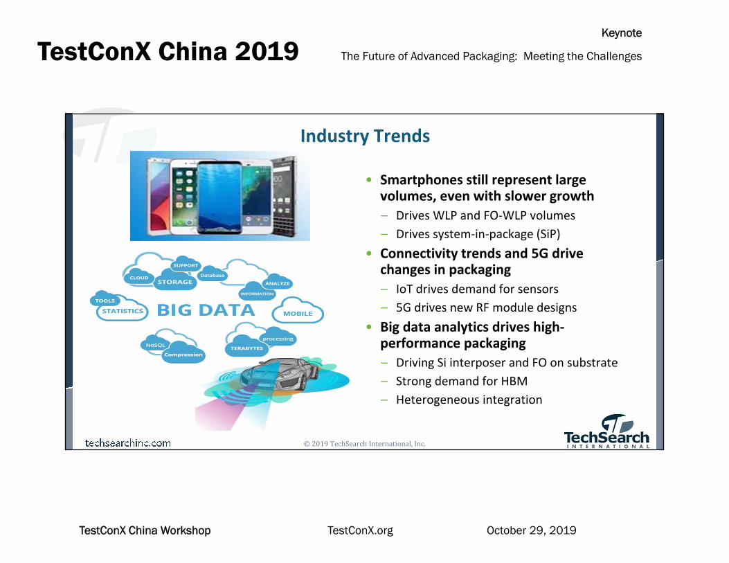
Industry Trends
• Smartphones still represent large volumes, even with slower growth– Drives WLP and FO-WLP volumes– Drives system-in-package (SiP)
• Connectivity trends and 5G drive changes in packaging– IoT drives demand for sensors– 5G drives new RF module designs
• Big data analytics drives high-performance packaging– Driving Si interposer and FO on substrate – Strong demand for HBM– Heterogeneous integration
The Future of Advanced Packaging: Meeting the ChallengesTestConX China 2019Keynote
October 29, 2019TestConX China Workshop TestConX.org
© 2019 TechSearch International, Inc.
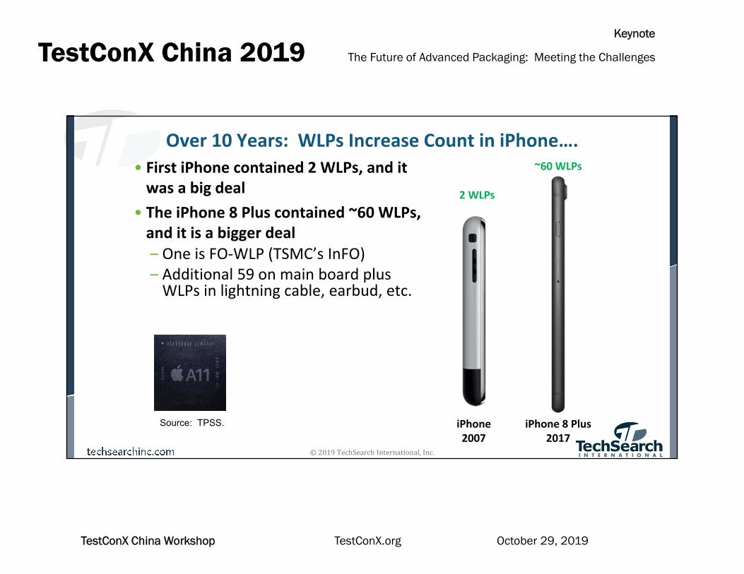
Over 10 Years: WLPs Increase Count in iPhone….• First iPhone contained 2 WLPs, and it
was a big deal• The iPhone 8 Plus contained ~60 WLPs,
and it is a bigger deal– One is FO-WLP (TSMC’s InFO)– Additional 59 on main board plus
WLPs in lightning cable, earbud, etc.
iPhone2007
2 WLPs
iPhone 8 Plus2017
~60 WLPs
Source: TPSS.

The Future of Advanced Packaging: Meeting the ChallengesTestConX China 2019Keynote
October 29, 2019TestConX China Workshop TestConX.org
© 2019 TechSearch International, Inc.
Migration to FO-WLP
FO-WLP (many versions)
FC-CSP
Fan-in WLP
The Future of Advanced Packaging: Meeting the ChallengesTestConX China 2019Keynote
October 29, 2019TestConX China Workshop TestConX.org
© 2019 TechSearch International, Inc.
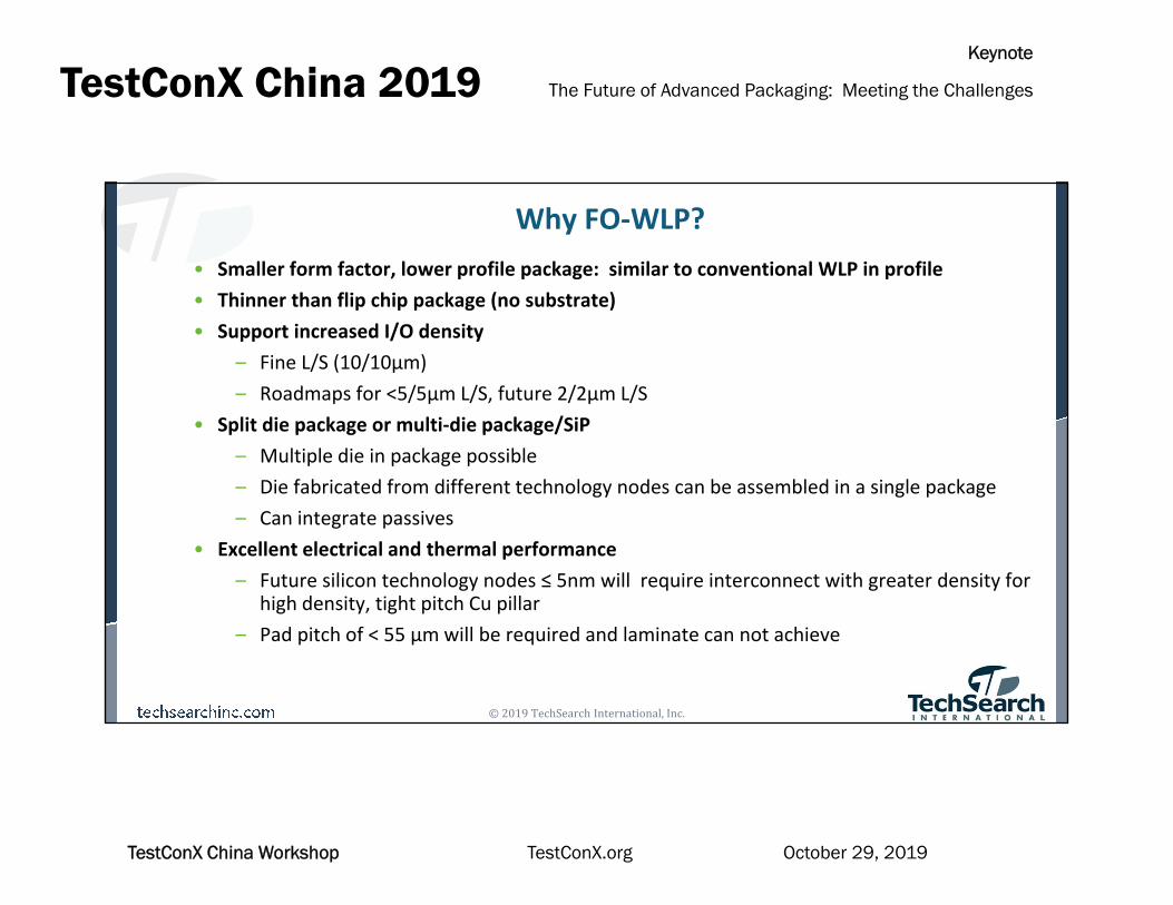
Why FO-WLP?• Smaller form factor, lower profile package: similar to conventional WLP in profile• Thinner than flip chip package (no substrate)• Support increased I/O density
– Fine L/S (10/10µm) – Roadmaps for <5/5µm L/S, future 2/2µm L/S
• Split die package or multi-die package/SiP– Multiple die in package possible– Die fabricated from different technology nodes can be assembled in a single package– Can integrate passives
• Excellent electrical and thermal performance– Future silicon technology nodes ≤ 5nm will require interconnect with greater density for
high density, tight pitch Cu pillar– Pad pitch of < 55 µm will be required and laminate can not achieve
The Future of Advanced Packaging: Meeting the ChallengesTestConX China 2019Keynote
October 29, 2019TestConX China Workshop TestConX.org
© 2019 TechSearch International, Inc.
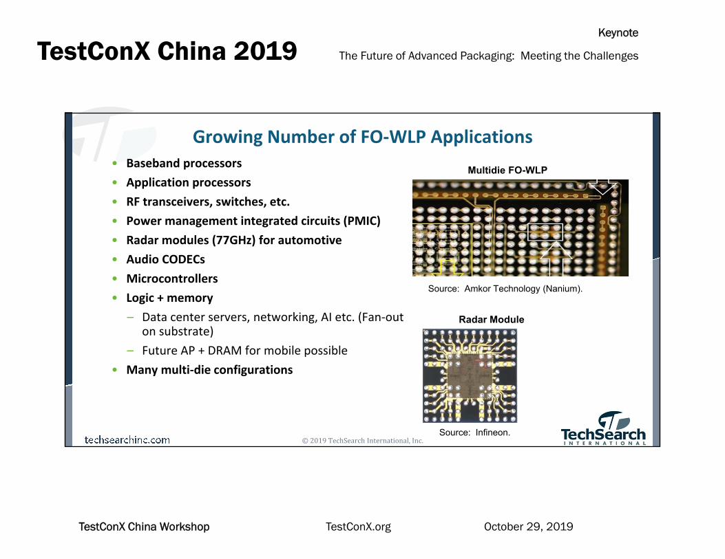
Growing Number of FO-WLP Applications• Baseband processors• Application processors• RF transceivers, switches, etc.• Power management integrated circuits (PMIC)• Radar modules (77GHz) for automotive • Audio CODECs• Microcontrollers• Logic + memory
– Data center servers, networking, AI etc. (Fan-out on substrate)
– Future AP + DRAM for mobile possible• Many multi-die configurations
Multidie FO-WLP
Source: Amkor Technology (Nanium).
Source: Infineon.
Radar Module

The Future of Advanced Packaging: Meeting the ChallengesTestConX China 2019Keynote
October 29, 2019TestConX China Workshop TestConX.org
© 2019 TechSearch International, Inc.
TSMC’s InFO for Apple’s Application Processors
Source: TSMC.
• Die-first, face-up process, RDL formed on top of Cu pillars on die• Improved electrical and thermal performance of InFO vs. FC-CSP• Thinner than flip chip package (no substrate)
– InFO-PoP is 20% thinner than FC-PoP, but thin is not only driver– Future silicon technology nodes 7nm and 5nm will require interconnect with greater density for high density,
tight pitch Cu pillar
Source: TSMC.
Source: TechInsights.
DRAM
TMVs
The Future of Advanced Packaging: Meeting the ChallengesTestConX China 2019Keynote
October 29, 2019TestConX China Workshop TestConX.org
© 2019 TechSearch International, Inc.
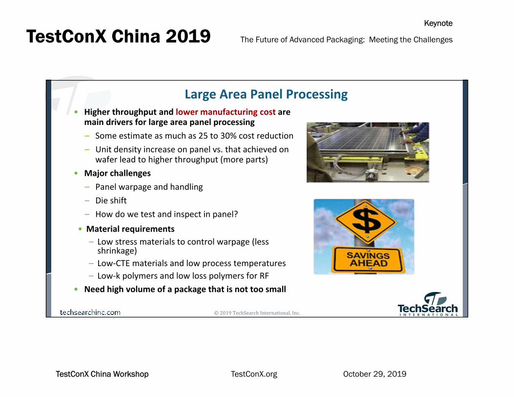
Large Area Panel Processing• Higher throughput and lower manufacturing cost are
main drivers for large area panel processing– Some estimate as much as 25 to 30% cost reduction– Unit density increase on panel vs. that achieved on
wafer lead to higher throughput (more parts)• Major challenges
– Panel warpage and handling– Die shift– How do we test and inspect in panel?
• Material requirements– Low stress materials to control warpage (less
shrinkage)– Low-CTE materials and low process temperatures– Low-k polymers and low loss polymers for RF
• Need high volume of a package that is not too small
The Future of Advanced Packaging: Meeting the ChallengesTestConX China 2019Keynote
October 29, 2019TestConX China Workshop TestConX.org
© 2019 TechSearch International, Inc.
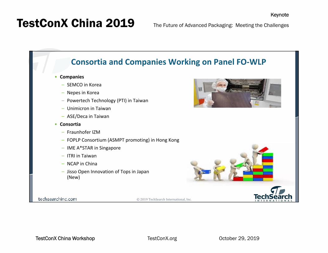
Consortia and Companies Working on Panel FO-WLP• Companies
– SEMCO in Korea– Nepes in Korea – Powertech Technology (PTI) in Taiwan– Unimicron in Taiwan– ASE/Deca in Taiwan
• Consortia– Fraunhofer IZM– FOPLP Consortium (ASMPT promoting) in Hong Kong– IME A*STAR in Singapore– ITRI in Taiwan– NCAP in China– Jisso Open Innovation of Tops in Japan
(New)
The Future of Advanced Packaging: Meeting the ChallengesTestConX China 2019Keynote
October 29, 2019TestConX China Workshop TestConX.org
© 2019 TechSearch International, Inc.
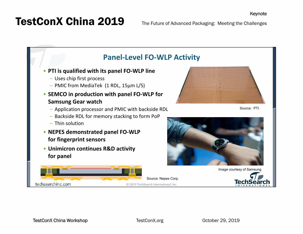
Panel-Level FO-WLP Activity• PTI is qualified with its panel FO-WLP line
– Uses chip first process– PMIC from MediaTek (1 RDL, 15µm L/S)
• SEMCO in production with panel FO-WLP for Samsung Gear watch– Application processor and PMIC with backside RDL– Backside RDL for memory stacking to form PoP– Thin solution
• NEPES demonstrated panel FO-WLP for fingerprint sensors
• Unimicron continues R&D activity for panel
Source: PTI.
Image courtesy of Samsung.
Source: Nepes Corp.
The Future of Advanced Packaging: Meeting the ChallengesTestConX China 2019Keynote
October 29, 2019TestConX China Workshop TestConX.org
© 2019 TechSearch International, Inc.
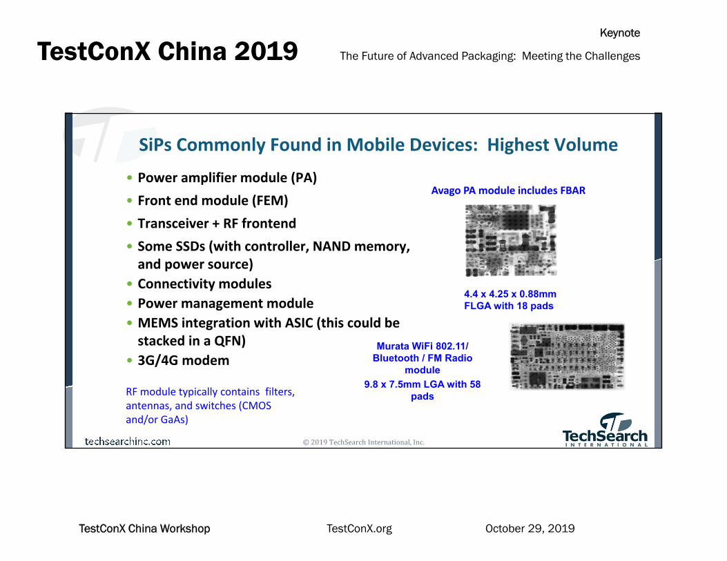
SiPs Commonly Found in Mobile Devices: Highest Volume• Power amplifier module (PA)• Front end module (FEM)• Transceiver + RF frontend• Some SSDs (with controller, NAND memory,
and power source)• Connectivity modules• Power management module• MEMS integration with ASIC (this could be
stacked in a QFN)• 3G/4G modem
RF module typically contains filters, antennas, and switches (CMOS and/or GaAs)
Avago PA module includes FBAR
4.4 x 4.25 x 0.88mmFLGA with 18 pads
Murata WiFi 802.11/ Bluetooth / FM Radio
module9.8 x 7.5mm LGA with 58
pads
The Future of Advanced Packaging: Meeting the ChallengesTestConX China 2019Keynote
October 29, 2019TestConX China Workshop TestConX.org
© 2019 TechSearch International, Inc.
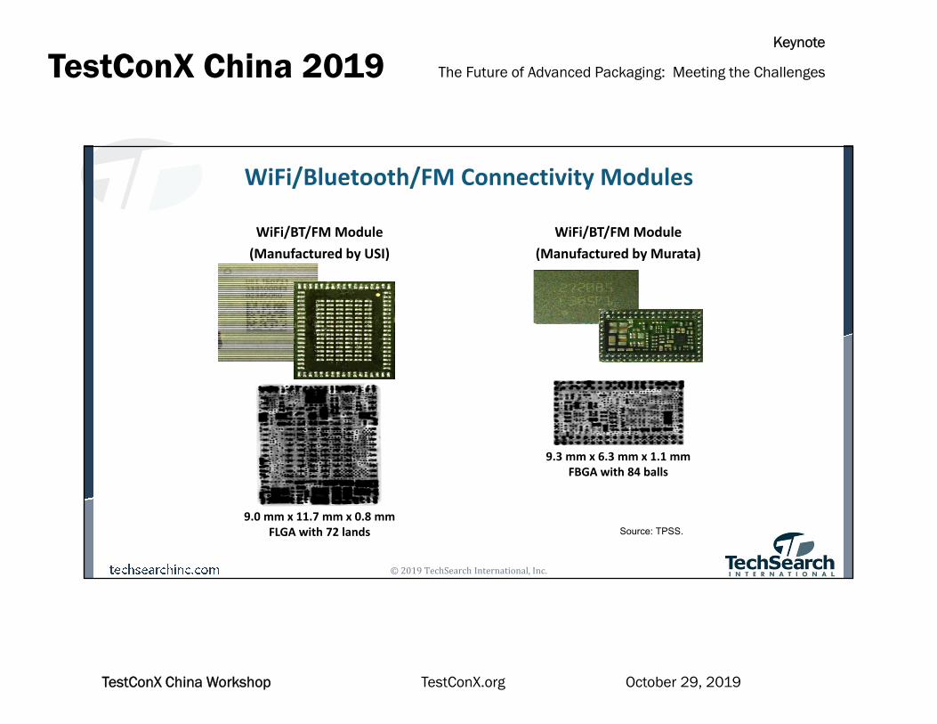
WiFi/Bluetooth/FM Connectivity Modules
WiFi/BT/FM Module(Manufactured by Murata)
9.3 mm x 6.3 mm x 1.1 mmFBGA with 84 balls
WiFi/BT/FM Module(Manufactured by USI)
9.0 mm x 11.7 mm x 0.8 mmFLGA with 72 lands Source: TPSS.
The Future of Advanced Packaging: Meeting the ChallengesTestConX China 2019Keynote
October 29, 2019TestConX China Workshop TestConX.org
© 2019 TechSearch International, Inc.
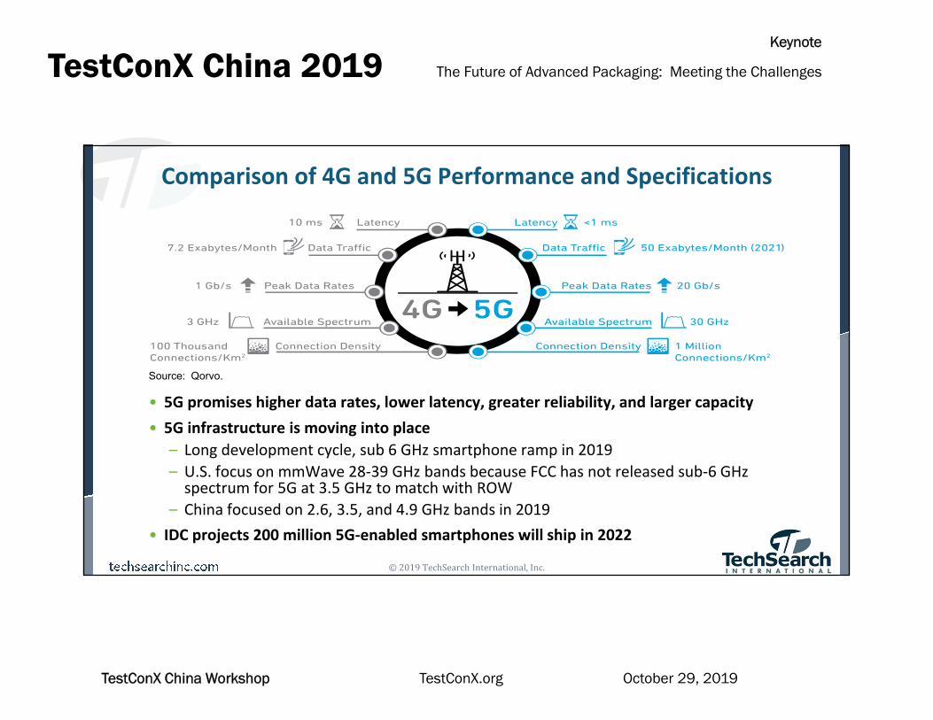
Comparison of 4G and 5G Performance and Specifications
• 5G promises higher data rates, lower latency, greater reliability, and larger capacity• 5G infrastructure is moving into place
– Long development cycle, sub 6 GHz smartphone ramp in 2019– U.S. focus on mmWave 28-39 GHz bands because FCC has not released sub-6 GHz
spectrum for 5G at 3.5 GHz to match with ROW– China focused on 2.6, 3.5, and 4.9 GHz bands in 2019
• IDC projects 200 million 5G-enabled smartphones will ship in 2022
Source: Qorvo.

The Future of Advanced Packaging: Meeting the ChallengesTestConX China 2019Keynote
October 29, 2019TestConX China Workshop TestConX.org
© 2019 TechSearch International, Inc.
Future Trends for RF Modules: 5G• 5G New Radio offers high bandwidth, low latency, and massive scalability of 5G
– High-performance baseband processors– Broadband, steerable, and high gain mmWave antennas– Efficient and broadband mmWave front-end ICs– RF components for co-design of mmWave antennas and front-end ICs with high-Q
inductors, filters, power dividers, phase shifters, and attenuators• 5G potentially means new radios, new modems, new PA, and new FEM
– Greater modularization expected– System-in-package designs with fully integrated antenna (so antenna design capabilities
are important)– Thermal and electrical modeling become more critical– Electromagnetic compatibility and EMI shielding become more important
• Test is critical

The Future of Advanced Packaging: Meeting the ChallengesTestConX China 2019Keynote
October 29, 2019TestConX China Workshop TestConX.org
© 2019 TechSearch International, Inc.
5G Drives New Test Approaches
• Most existing test and commercial 5G networks exist in the sub-6 GHz range– Requires some adjustment in software, networks, antenna configuration and other functions– Only as much change as moving from 3G to 4G
• 5G advantage comes from shift to mmWave frequencies above 24GHz– These frequencies provide more bandwidth than other frequencies– With mmWave the package is the antenna
• 5G capabilities rely on advanced networking capabilities– Beam-forming (vs. previous generation of omnidirectional or wide-beam antennas)– Phased arrays (must be able to send and receive shaped waveforms tested under realistic conditions)– Massive Multiple-input/multiple-output (mMIMO)
• Discussions about over-the-air test– Some similarities with what is done in automotive radar
• Concerns– Lack of automated test equipment – Pressure to move 5G products to market driving many to cobble together own solutions using network
analyzers or high-frequency RF analyzers
The Future of Advanced Packaging: Meeting the ChallengesTestConX China 2019Keynote
October 29, 2019TestConX China Workshop TestConX.org
© 2019 TechSearch International, Inc.
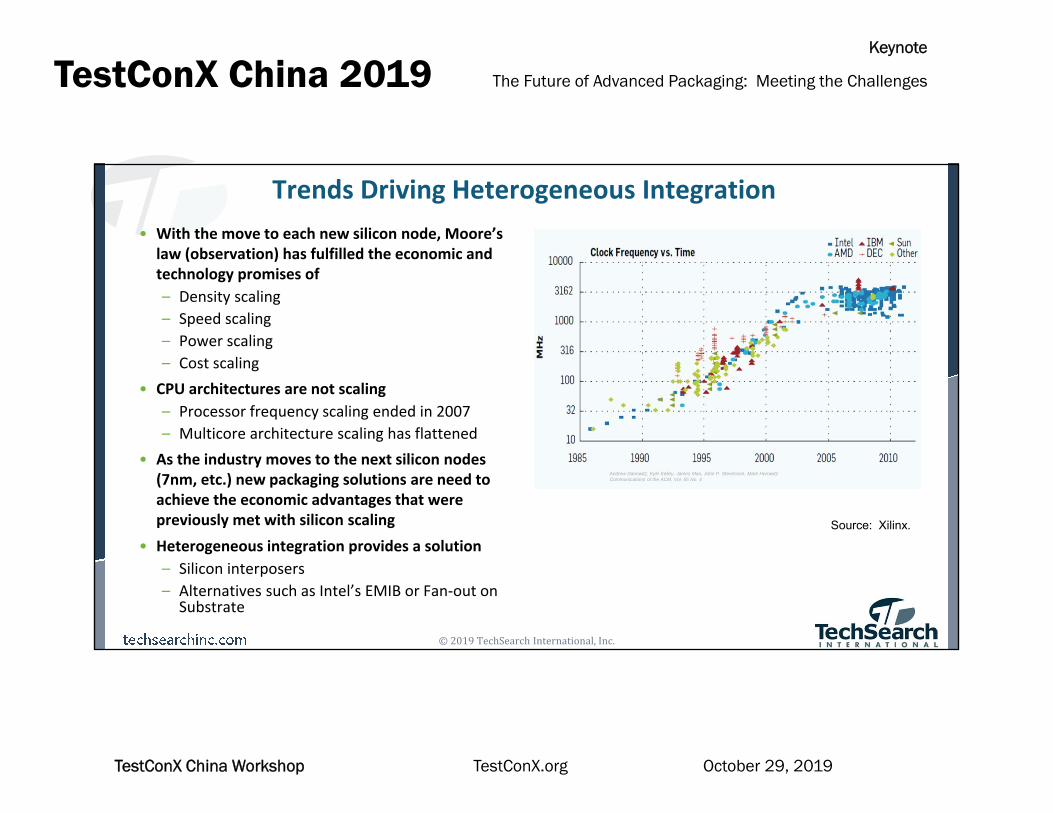
Trends Driving Heterogeneous Integration• With the move to each new silicon node, Moore’s
law (observation) has fulfilled the economic and technology promises of– Density scaling– Speed scaling– Power scaling– Cost scaling
• CPU architectures are not scaling– Processor frequency scaling ended in 2007– Multicore architecture scaling has flattened
• As the industry moves to the next silicon nodes (7nm, etc.) new packaging solutions are need to achieve the economic advantages that were previously met with silicon scaling
• Heterogeneous integration provides a solution – Silicon interposers– Alternatives such as Intel’s EMIB or Fan-out on
Substrate
Andrew Danowitz, Kyle Kelley, James Mao, John P. Stevenson, Mark Horowitz Communications of the ACM, Vol. 55 No. 4
Source: Xilinx.
The Future of Advanced Packaging: Meeting the ChallengesTestConX China 2019Keynote
October 29, 2019TestConX China Workshop TestConX.org
© 2019 TechSearch International, Inc.
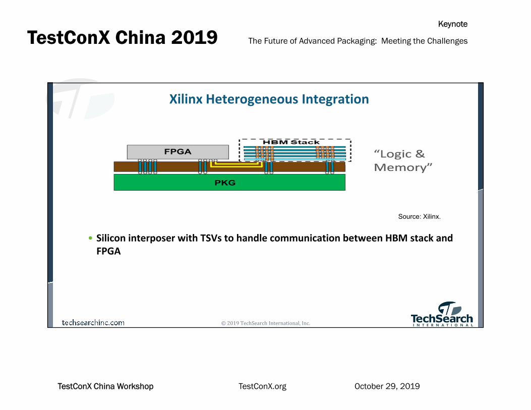
Xilinx Heterogeneous Integration
• Silicon interposer with TSVs to handle communication between HBM stack and FPGA
Source: Xilinx.

The Future of Advanced Packaging: Meeting the ChallengesTestConX China 2019Keynote
October 29, 2019TestConX China Workshop TestConX.org
© 2019 TechSearch International, Inc.
What’s Driving Demand for Si Interposers?
• AI accelerators in datacenters to increase to 50% by 2020
• Network systems• Graphics market
Source: NVIDIA.
Source: Intel.
The Future of Advanced Packaging: Meeting the ChallengesTestConX China 2019Keynote
October 29, 2019TestConX China Workshop TestConX.org
© 2019 TechSearch International, Inc.
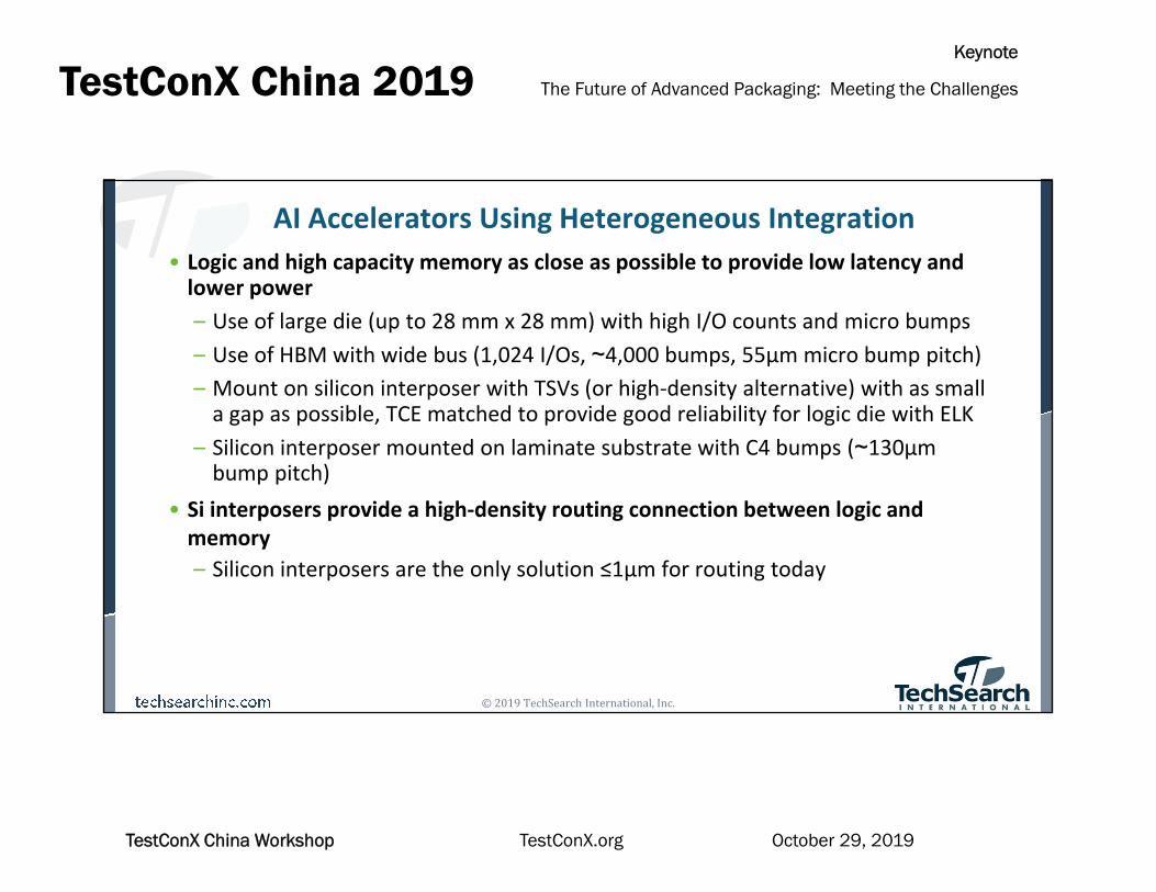
AI Accelerators Using Heterogeneous Integration• Logic and high capacity memory as close as possible to provide low latency and
lower power– Use of large die (up to 28 mm x 28 mm) with high I/O counts and micro bumps– Use of HBM with wide bus (1,024 I/Os, ~4,000 bumps, 55µm micro bump pitch)– Mount on silicon interposer with TSVs (or high-density alternative) with as small
a gap as possible, TCE matched to provide good reliability for logic die with ELK– Silicon interposer mounted on laminate substrate with C4 bumps (~130µm
bump pitch)• Si interposers provide a high-density routing connection between logic and
memory– Silicon interposers are the only solution ≤1µm for routing today
The Future of Advanced Packaging: Meeting the ChallengesTestConX China 2019Keynote
October 29, 2019TestConX China Workshop TestConX.org
© 2019 TechSearch International, Inc.
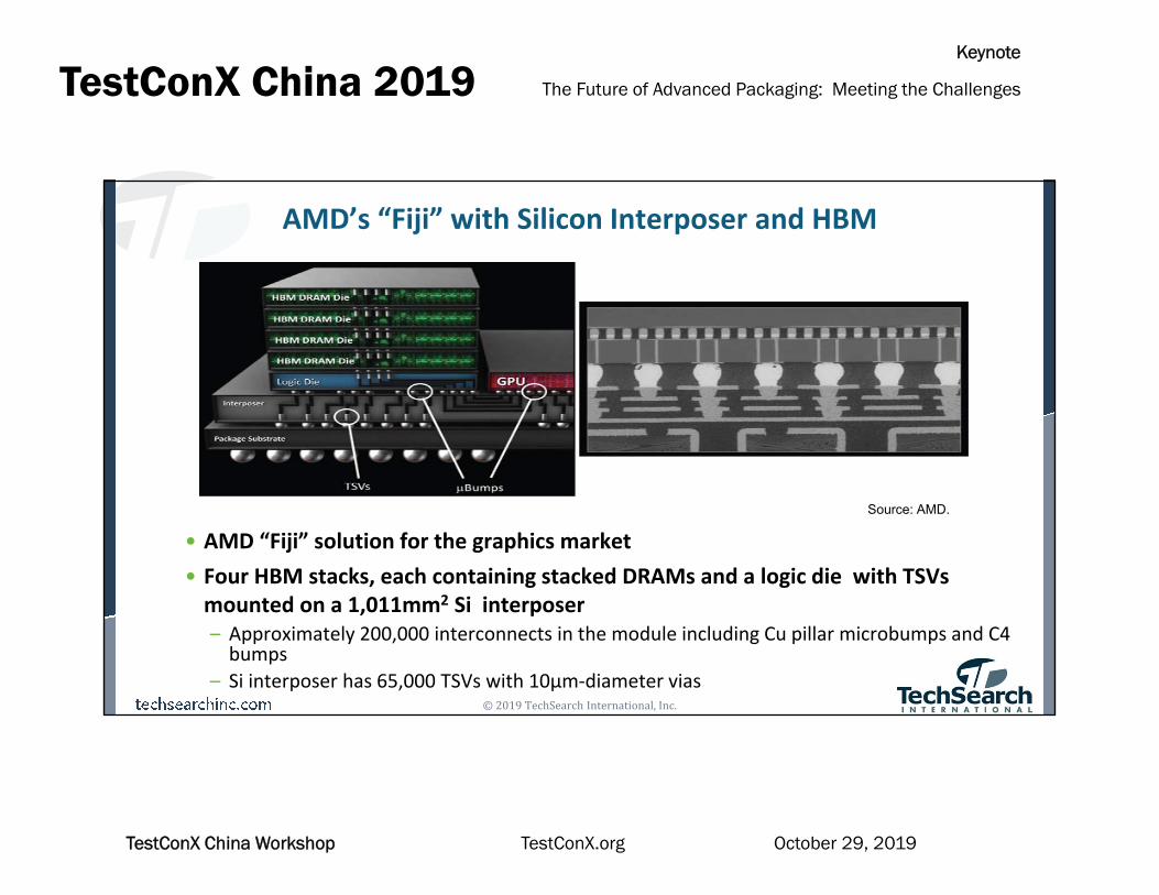
AMD’s “Fiji” with Silicon Interposer and HBM
• AMD “Fiji” solution for the graphics market• Four HBM stacks, each containing stacked DRAMs and a logic die with TSVs
mounted on a 1,011mm2 Si interposer– Approximately 200,000 interconnects in the module including Cu pillar microbumps and C4
bumps– Si interposer has 65,000 TSVs with 10µm-diameter vias
Source: AMD.

The Future of Advanced Packaging: Meeting the ChallengesTestConX China 2019Keynote
October 29, 2019TestConX China Workshop TestConX.org
© 2019 TechSearch International, Inc.
Test Strategy: Key To AMD Success
• Wafer sort (important to consider probe tip, pad size, and control of probe mark)• Partial assembly test (unique to this application, LGA pad surface finish, contact
force control, yield repeatability, and contamination control)• Final test (thermal management important)
Source: ASE and AMD.
The Future of Advanced Packaging: Meeting the ChallengesTestConX China 2019Keynote
October 29, 2019TestConX China Workshop TestConX.org
© 2019 TechSearch International, Inc.
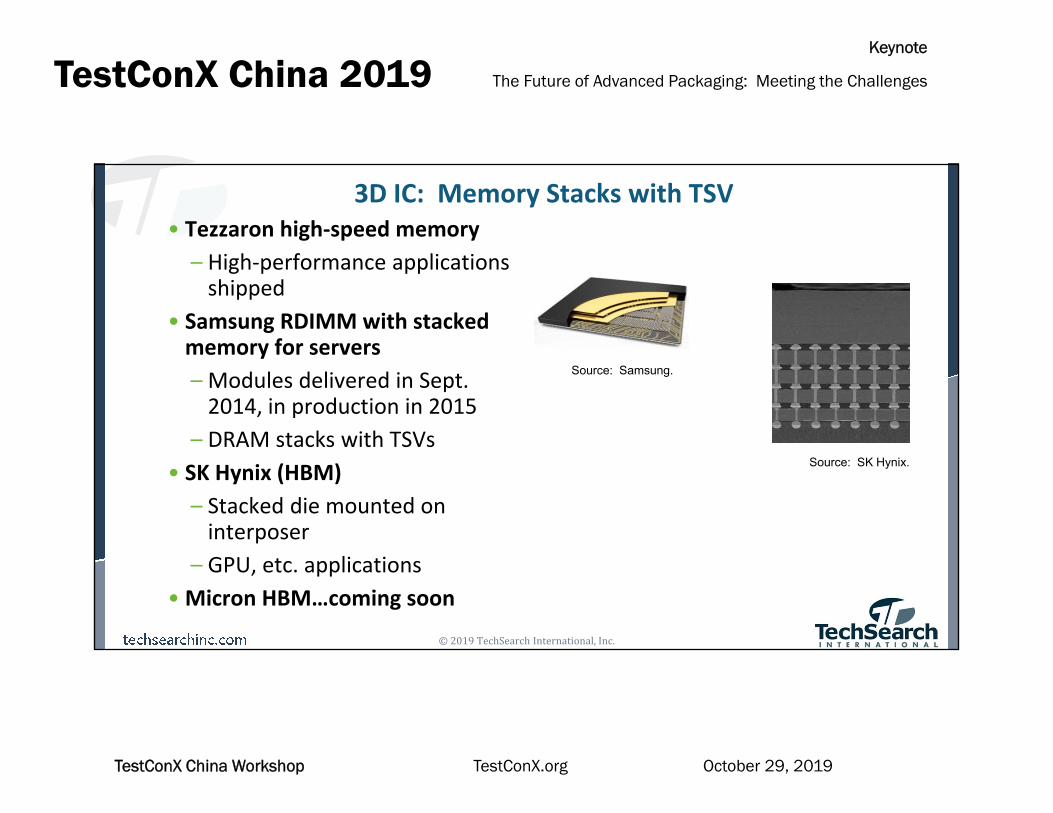
3D IC: Memory Stacks with TSV• Tezzaron high-speed memory
– High-performance applications shipped
• Samsung RDIMM with stacked memory for servers– Modules delivered in Sept.
2014, in production in 2015– DRAM stacks with TSVs
• SK Hynix (HBM)– Stacked die mounted on
interposer– GPU, etc. applications
• Micron HBM…coming soon
Source: Samsung.
Source: SK Hynix.

The Future of Advanced Packaging: Meeting the ChallengesTestConX China 2019Keynote
October 29, 2019TestConX China Workshop TestConX.org
© 2019 TechSearch International, Inc.
HBM Test and Test Vehicle Development
• Stacked die with TSVs requirements– Well joined TSV/micro bumps– Well aligned micro bumps– No underfill delamination or voids
• Test vehicles TSV stacked memory– Robustness of TSVs and micro bumps important– All test patterns electrically tested in test vehicles
• Bump pitch– Bottom die bump diameter 25µm– Bottom die bump pitch 55µm staggered for HBM
versus 100µm for HMC– Bump pitch between die 40 µm (Cu pillar)
The Future of Advanced Packaging: Meeting the ChallengesTestConX China 2019Keynote
October 29, 2019TestConX China Workshop TestConX.org
© 2019 TechSearch International, Inc.
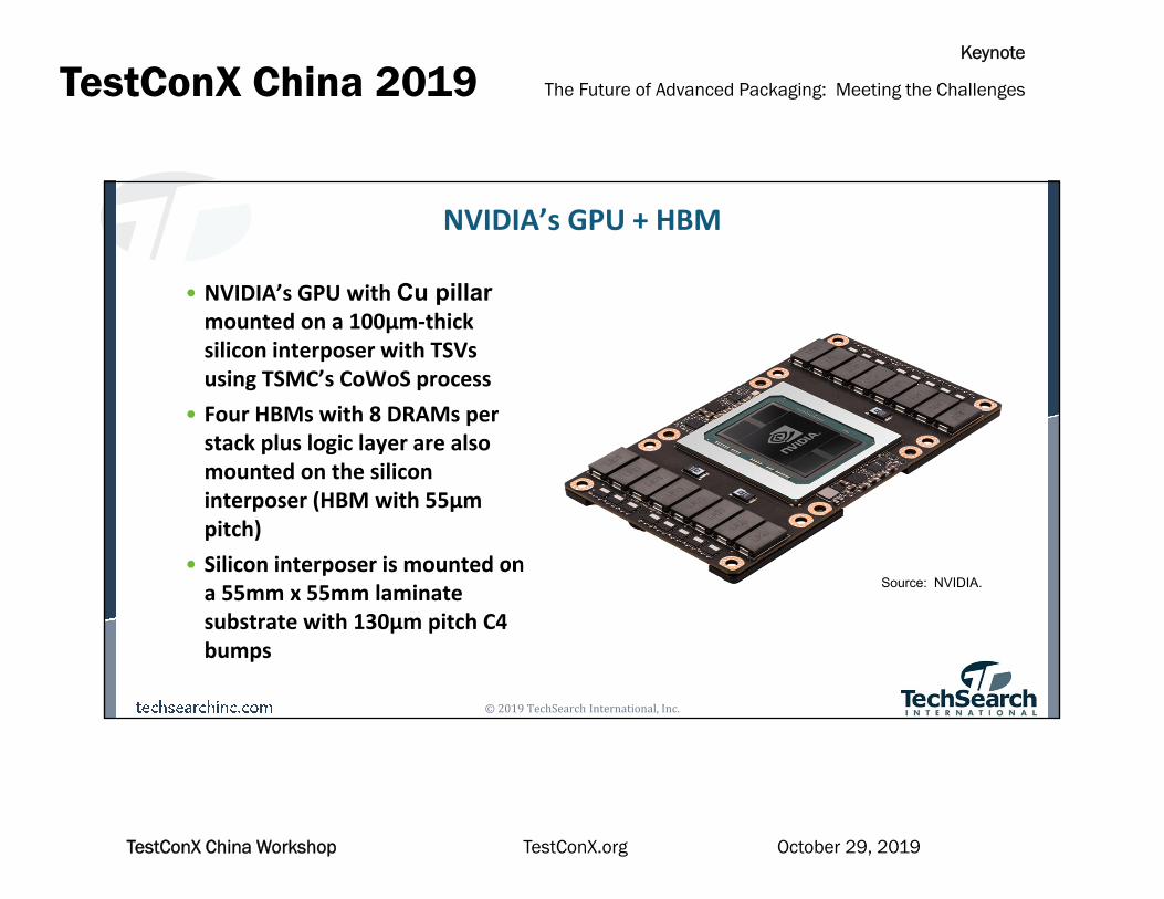
NVIDIA’s GPU + HBM
• NVIDIA’s GPU with Cu pillarmounted on a 100µm-thick silicon interposer with TSVs using TSMC’s CoWoS process
• Four HBMs with 8 DRAMs per stack plus logic layer are also mounted on the silicon interposer (HBM with 55µm pitch)
• Silicon interposer is mounted on a 55mm x 55mm laminate substrate with 130µm pitch C4 bumps
Source: NVIDIA.
The Future of Advanced Packaging: Meeting the ChallengesTestConX China 2019Keynote
October 29, 2019TestConX China Workshop TestConX.org
© 2019 TechSearch International, Inc.
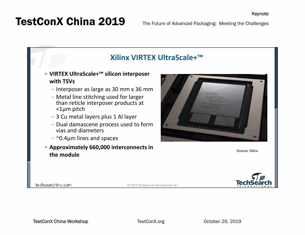
Xilinx VIRTEX UltraScale+™
• VIRTEX UltraScale+™ silicon interposer with TSVs– Interposer as large as 30 mm x 36 mm– Metal line stitching used for larger
than reticle interposer products at <1µm pitch
– 3 Cu metal layers plus 1 Al layer– Dual damascene process used to form
vias and diameters– ~0.4µm lines and spaces
• Approximately 660,000 interconnects in the module
Source: Xilinx.

The Future of Advanced Packaging: Meeting the ChallengesTestConX China 2019Keynote
October 29, 2019TestConX China Workshop TestConX.org
© 2019 TechSearch International, Inc.
Google Tensor Processing Unit v2 with Interposer and HBM
• Google-designed device for neural net training and inference– 16 GB of HBM– 600 GB/s memory bandwidth
• ASIC + HBM on Si interposer using TSMC’s CoWoS
• Version 3, introduced in May 2018, doubled the HBM

The Future of Advanced Packaging: Meeting the ChallengesTestConX China 2019Keynote
October 29, 2019TestConX China Workshop TestConX.org
© 2019 TechSearch International, Inc.
Intel’s Silicon Bridge
• Embedded Multi-die Interconnect Bridge (EMIB) A small silicon bridge chip is embedded into the package (no TSVs)– Package substrate provided by substrate supplier (does Si bridge embedding)
• Considered less expensive because only small area for high-density silicon and no TSVs• EMIB allows the die I/O or bumps to be placed as close as possible to the edge of the die because fewer I/O or
bumps are required– Micro bumps on chips, communication between chips through interposer
• Good electrical performance is reported due to the short interconnects
Source: Intel.

The Future of Advanced Packaging: Meeting the ChallengesTestConX China 2019Keynote
October 29, 2019TestConX China Workshop TestConX.org
© 2019 TechSearch International, Inc.
Heterogeneous Integration Using EMIB Technology
• Stratix 10MX FPGA product with integration of HBM2 uses EMIB• Stratix FPGA on 14nm FinFET silicon node• Intel purchased Altera in 2015
Source: Intel.

The Future of Advanced Packaging: Meeting the ChallengesTestConX China 2019Keynote
October 29, 2019TestConX China Workshop TestConX.org
© 2019 TechSearch International, Inc.
Growth in FO-WLP on Substrate• ASE’s Fan-Out Chip on Substrate (FOCoS)
– RDL with 2µm/2.5 L/S– Up to 3 RDLs plus UBM– High I/O (>1,000)– Production for Hi-Silicon since 2016, new customers expected
• TSMC Integrated Fan-Out WLP on Substrate (InFO_oS)– RDL with 2µm L/S– Up to 3 RDLs plus UBM– In production or MediaTek Switch
• Amkor’s Silicon Wafer Integrated Fan-out Technology (SWIFT®) – RDL with 2/2µm L/S– Up to 3 RDLs plus UBM– Potential customers in 2019
Source: ASE.
The Future of Advanced Packaging: Meeting the ChallengesTestConX China 2019Keynote
October 29, 2019TestConX China Workshop TestConX.org
© 2019 TechSearch International, Inc.
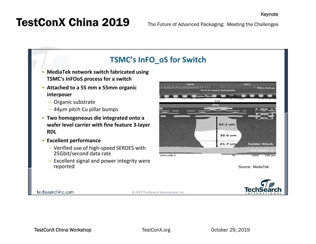
TSMC’s InFO_oS for Switch• MediaTek network switch fabricated using
TSMC’s InFOoS process for a switch• Attached to a 55 mm x 55mm organic
interposer– Organic substrate– 44µm pitch Cu pillar bumps
• Two homogeneous die integrated onto a wafer level carrier with fine feature 3-layer RDL
• Excellent performance– Verified use of high-speed SERDES with
25Gbit/second data rate– Excellent signal and power integrity were
reported Source: MediaTek.
The Future of Advanced Packaging: Meeting the ChallengesTestConX China 2019Keynote
October 29, 2019TestConX China Workshop TestConX.org
© 2019 TechSearch International, Inc.
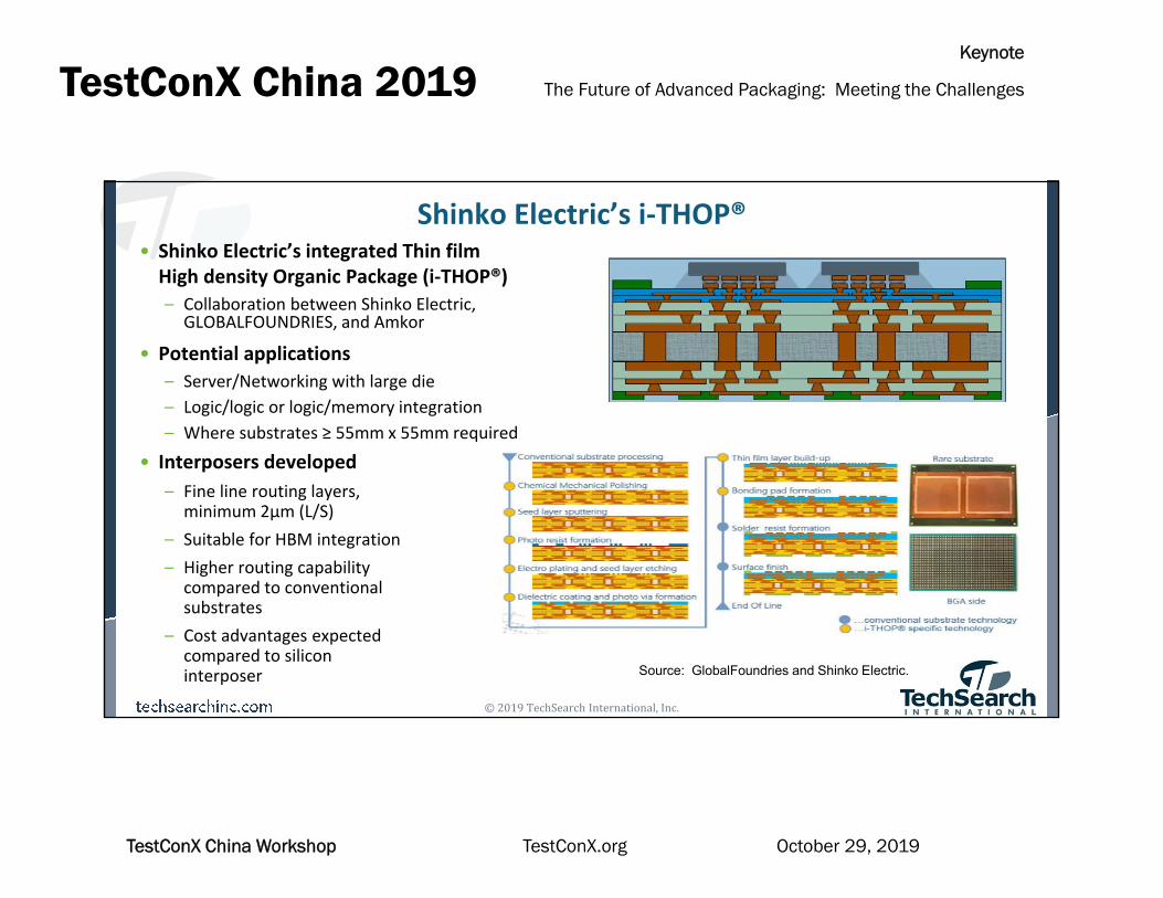
Shinko Electric’s i-THOP®• Shinko Electric’s integrated Thin film
High density Organic Package (i-THOP®)– Collaboration between Shinko Electric,
GLOBALFOUNDRIES, and Amkor
• Potential applications– Server/Networking with large die– Logic/logic or logic/memory integration– Where substrates ≥ 55mm x 55mm required
• Interposers developed– Fine line routing layers,
minimum 2μm (L/S) – Suitable for HBM integration – Higher routing capability
compared to conventional substrates
– Cost advantages expected compared to siliconinterposer Source: GlobalFoundries and Shinko Electric.
The Future of Advanced Packaging: Meeting the ChallengesTestConX China 2019Keynote
October 29, 2019TestConX China Workshop TestConX.org
© 2019 TechSearch International, Inc.
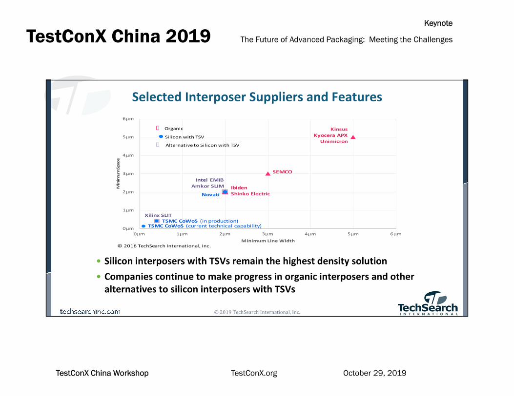
Selected Interposer Suppliers and Features
• Silicon interposers with TSVs remain the highest density solution• Companies continue to make progress in organic interposers and other
alternatives to silicon interposers with TSVs
0µm
1µm
2µm
3µm
4µm
5µm
6µm
0µm 1µm 2µm 3µm 4µm 5µm 6µm
Min
imum
Spac
e
Minimum Line Width
KinsusKyocera APX
Unimicron
SEMCOIntel EMIB
Amkor SLIM
Xilinx SLIT
TSMC CoWoS (current technical capability)
NovatiIbidenShinko Electric
Organic
● Silicon with TSV
Alternative to Silicon with TSV
TSMC CoWoS (in production)
© 2016 TechSearch International, Inc.
The Future of Advanced Packaging: Meeting the ChallengesTestConX China 2019Keynote
October 29, 2019TestConX China Workshop TestConX.org
© 2019 TechSearch International, Inc.
Test Challenges for Heterogeneous Integration
• Known Good Die (KGD) required• Known Good Substrate needed• Know Good Interconnect (assumed)• Need more comprehensive test content that can be run at wafer-level• Need new methods to probe fine pitch bumps or test coverage without touching
µbumps
The Future of Advanced Packaging: Meeting the ChallengesTestConX China 2019Keynote
October 29, 2019TestConX China Workshop TestConX.org
© 2019 TechSearch International, Inc.
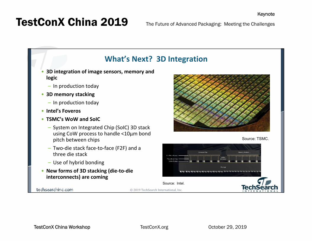
• 3D integration of image sensors, memory and logic– In production today
• 3D memory stacking– In production today
• Intel’s Foveros• TSMC’s WoW and SoIC
– System on Integrated Chip (SoIC) 3D stack using CoW process to handle <10µm bond pitch between chips
– Two-die stack face-to-face (F2F) and a three die stack
– Use of hybrid bonding• New forms of 3D stacking (die-to-die
interconnects) are coming
What’s Next? 3D Integration
Source: TSMC.
Source: Intel.
The Future of Advanced Packaging: Meeting the ChallengesTestConX China 2019Keynote
October 29, 2019TestConX China Workshop TestConX.org
© 2019 TechSearch International, Inc.
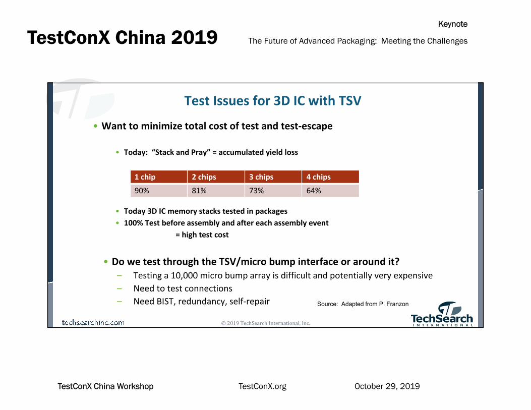
Test Issues for 3D IC with TSV• Want to minimize total cost of test and test-escape
• Today: “Stack and Pray” = accumulated yield loss
• Today 3D IC memory stacks tested in packages• 100% Test before assembly and after each assembly event
= high test cost
• Do we test through the TSV/micro bump interface or around it?– Testing a 10,000 micro bump array is difficult and potentially very expensive– Need to test connections– Need BIST, redundancy, self-repair
1 chip 2 chips 3 chips 4 chips90% 81% 73% 64%
Source: Adapted from P. Franzon
The Future of Advanced Packaging: Meeting the ChallengesTestConX China 2019Keynote
October 29, 2019TestConX China Workshop TestConX.org
© 2019 TechSearch International, Inc.
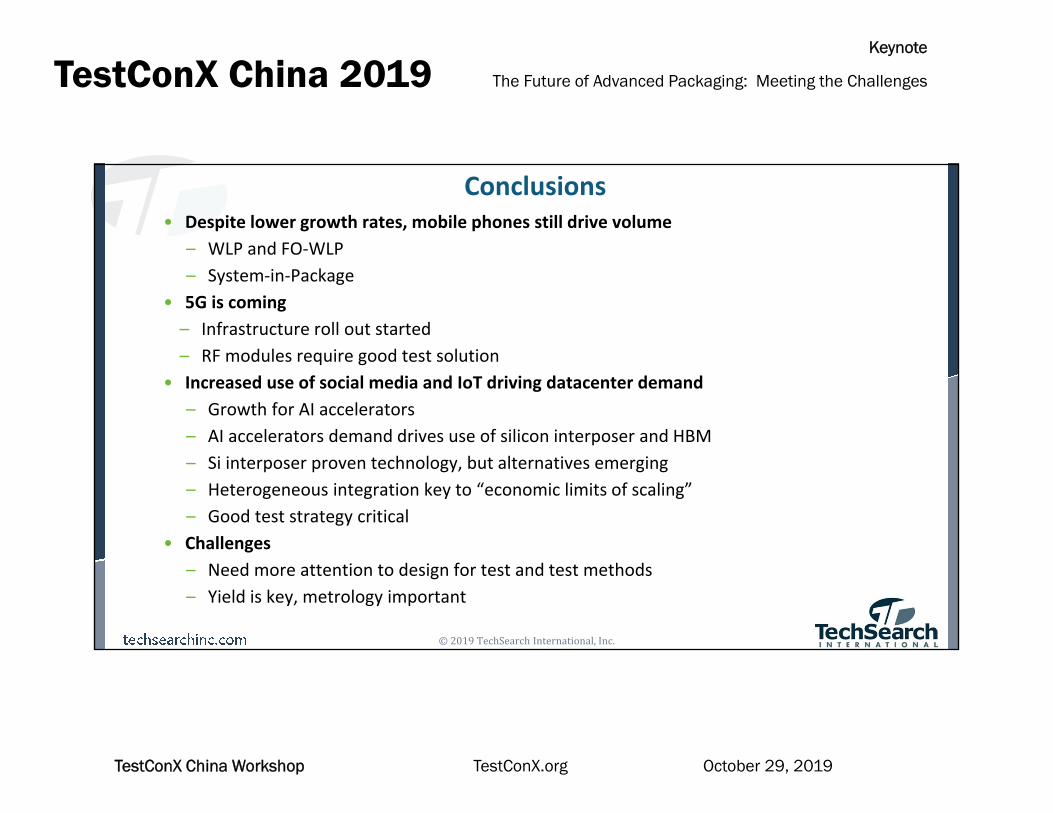
Conclusions• Despite lower growth rates, mobile phones still drive volume
– WLP and FO-WLP– System-in-Package
• 5G is coming – Infrastructure roll out started– RF modules require good test solution
• Increased use of social media and IoT driving datacenter demand– Growth for AI accelerators– AI accelerators demand drives use of silicon interposer and HBM– Si interposer proven technology, but alternatives emerging– Heterogeneous integration key to “economic limits of scaling”– Good test strategy critical
• Challenges– Need more attention to design for test and test methods– Yield is key, metrology important

The Future of Advanced Packaging: Meeting the ChallengesTestConX China 2019Keynote
October 29, 2019TestConX China Workshop TestConX.org
TechSearch International, Inc.4801 Spicewood Springs Road, Suite 150
Austin, Texas 78759 USA+1.512.372.8887
Thank you!
© 2018 TechSearch International, Inc.
COPYRIGHT NOTICEThe presentation(s)/poster(s) in this publication comprise the Proceedings of the 2019 TestConX China workshop. The content reflects the opinion of the authors and their respective companies. They are reproduced here as they were presented at the 2019 TestConX China workshop. This version of the presentation or poster may differ from the version that was distributed in hardcopy & softcopy form at the 2019 TestConX China workshop. The inclusion of the presentations/posters in this publication does not constitute an endorsement by TestConX or the workshop’s sponsors.
There is NO copyright protection claimed on the presentation/poster content by TestConX. However, each presentation/poster is the work of the authors and their respective companies: as such, it is strongly encouraged that any use reflect proper acknowledgement to the appropriate source. Any questions regarding the use of any materials presented should be directed to the author(s) or their companies.
The TestConX China logo and TestConX logo are trademarks of TestConX. All rights reserved.
www.TestConX.org


![WELCOME [ihg.scene7.com]...InterContinental Shanghai Pudong provides an innovative ‘Five Senses’ break, introducing Mr. Ru Bing Sheng, one of the first scholars to explore the](https://img.pdfslide.net/doc/110x75/5edcebbcad6a402d6667cf14/welcome-ihg-intercontinental-shanghai-pudong-provides-an-innovative-afive.jpg)