Embed Size (px)
Citation preview
HAL Id: hal-01489186https://hal.archives-ouvertes.fr/hal-01489186
Submitted on 14 Mar 2017
HAL is a multi-disciplinary open accessarchive for the deposit and dissemination of sci-entific research documents, whether they are pub-lished or not. The documents may come fromteaching and research institutions in France orabroad, or from public or private research centers.
L’archive ouverte pluridisciplinaire HAL, estdestinée au dépôt et à la diffusion de documentsscientifiques de niveau recherche, publiés ou non,émanant des établissements d’enseignement et derecherche français ou étrangers, des laboratoirespublics ou privés.
On-chip and freestanding elastic carbon films formicro-supercapacitors
Peihua Huang, Christophe Lethien, Sébastien Pinaud, Kevin Brousse,Raphaël Laloo, Viviane Turq, Marc Respaud, Arnaud Demortiere, Barbara
Daffos, Pierre-Louis Taberna, et al.
To cite this version:Peihua Huang, Christophe Lethien, Sébastien Pinaud, Kevin Brousse, Raphaël Laloo, et al.. On-chipand freestanding elastic carbon films for micro-supercapacitors. Science, American Association for theAdvancement of Science, 2016, 351 (6274), pp.691-695. �10.1126/science.aad3345�. �hal-01489186�
Open Archive TOULOUSE Archive Ouverte (OATAO) OATAO is an open access repository that collects the work of Toulouse researchers and makes it freely available over the web where possible.
This is an author-deposited version published in : http://oatao.univ-toulouse.fr/ Eprints ID : 16766
To link to this article : DOI:10.1126/science.aad3345 URL : http://dx.doi.org/10.1126/science.aad3345
To cite this version : Huang, Peihua and Lethien, Christophe and Pinaud, Sébastien and Brousse, Kevin and Laloo, Raphaël and Turq, Viviane and Respaud, Marc and Demortiere, Arnaud and Daffos, Barbara and Taberna, Pierre-Louis and Chaudret, Bruno and Gogotsi, Yury and Simon, Patrice On-chip and freestanding elastic carbon films for micro-supercapacitors. (2016) Science Magazine, vol. 351 (n° 6274). pp. 691-695. ISSN 0036-8075
Any correspondence concerning this service should be sent to the repository
administrator: [email protected]

22. G. D. Gilliland et al., Phys. Rev. Lett. 71, 3717–3720(1993).
23. D. Xiao, G. B. Liu, W. Feng, X. Xu, W. Yao, Phys. Rev. Lett. 108,196802 (2012).
24. W.-T. Hsu et al., ACS Nano 8, 2951–2958(2014).
25. A. M. van der Zande et al., Nano Lett. 14, 3869–3875(2014).
26. K. Liu et al., Nat. Commun. 5, 4966 (2014).27. H. Yu, Y. Wang, Q. Tong, X. Xu, W. Yao, Phys. Rev. Lett. 115,
187002 (2015).28. T. Cao et al., Nat. Commun. 3, 887 (2012).29. K. F. Mak, K. He, J. Shan, T. F. Heinz, Nat. Nanotechnol. 7,
494–498 (2012).30. H. Zeng, J. Dai, W. Yao, D. Xiao, X. Cui, Nat. Nanotechnol. 7,
490–493 (2012).31. M. M. Fogler, L. V. Butov, K. S. Novoselov, Nat. Commun. 5,
4555 (2014).32. P. J. Zomer, M. H. D. Guimarães, J. C. Brant, N. Tombros,
B. J. van Wees, Appl. Phys. Lett. 105, 013101 (2014).
33. Materials and methods are available as supplementarymaterials on Science Online.
34. C. Mai et al., Nano Lett. 14, 202–206 (2014).35. Q. Wang et al., ACS Nano 7, 11087–11093
(2013).36. C. R. Zhu et al., Phys. Rev. B 90, 161302
(2014).
ACKNOWLEDGMENTS
We thank D. Cobden and F. Wang for helpful discussion. This workis mainly supported by the U.S. Department of Energy (DOE), BasicEnergy Sciences (BES), Materials Sciences and EngineeringDivision (DE-SC0008145 and SC0012509). The spectroscopy workis partially supported by NSF-EFRI-1433496. H.Y. and W.Y. weresupported by the Croucher Foundation (Croucher InnovationAward), and the Research Grants Counciland University GrantsCommittee of Hong Kong (HKU17305914P, HKU9/CRF/13G, AoE/P-04/08). J.Y. and D.G.M. were supported by the DOE, BES,Materials Sciences and Engineering Division. X.X. acknowledges aCottrell Scholar Award and support from the State of Washington–
funded Clean Energy Institute. Device fabrication was performedat the University of Washington Microfabrication Facility andNSF-funded Nanotech User Facility. Data described in this paperare presented in the supplementary materials and are availableupon request. X.X. and W.Y. conceived and supervised the project.P.R. and K.L.S. fabricated the samples and performed theexperiments, assisted by J.R.S. P.R., K.L.S., and X.X. analyzed data.H.Y. and W.Y. provided theoretical support and performed thesimulation. J.Y. and D.G.M. synthesized and characterized the bulkcrystal. P.R., K.L.S., X.X., W.Y., and H.Y. cowrote the paper. Allauthors discussed the results.
SUPPLEMENTARY MATERIALS
www.sciencemag.org/content/351/6274/688/suppl/DC1Materials and MethodsFigs. S1 to S15References (37–45)
On-chip and freestanding elasticcarbon films for micro-supercapacitorsP. Huang,1,2 C. Lethien,2,3 S. Pinaud,4 K. Brousse,1,2 R. Laloo,1,2 V. Turq,1,2 M. Respaud,4,5
A. Demortière,2,6 B. Daffos,1,2 P. L. Taberna,1,2 B. Chaudret,4 Y. Gogotsi,7 P. Simon1,2*
Integration of electrochemical capacitors with silicon-based electronics is a majorchallenge, limiting energy storage on a chip. We describe a wafer-scale process formanufacturing strongly adhering carbide-derived carbon films and interdigitatedmicro-supercapacitors with embedded titanium carbide current collectors, fullycompatible with current microfabrication and silicon-based device technology.Capacitance of those films reaches 410 farads per cubic centimeter/200 millifaradsper square centimeter in aqueous electrolyte and 170 farads per cubic centimeter/85millifarads per square centimeter in organic electrolyte. We also demonstrate preparationof self-supported, mechanically stable, micrometer-thick porous carbon films with aYoung’s modulus of 14.5 gigapascals, with the possibility of further transfer ontoflexible substrates. These materials are interesting for applications in structural energystorage, tribology, and gas separation.
The plethora of portable electronic devicesand the continued expansion of electronicsinto new mobile applications highlightthe need for high-performance miniatur-ized electrochemical storage devices able
to deliver energy from their environment. Radiofrequency identification (RFID) tags for the devel-opment of smart environments are another crit-ical application that requires compact energystorage. Accordingly, designing efficient mini-aturized energy storage devices for energy de-livery or harvesting with high-power capabilitiesremains a challenge (1).Electrochemical double-layer capacitors (EDLCs),
also known as supercapacitors, store the chargethrough reversible ion adsorption at the surfaceof high-surface-area carbons. Aside from an out-standing cycle life, this electrostatic charge stor-age results in devices with medium energydensity (~6 W·h kg−1) and high power densities(>10 kW kg−1). As a result, supercapacitorscomplement—or can even sometimes replace—batteries in applications from electronics topublic transportation and renewable energy stor-
age, in which high-power delivery and uptakeand very long cycle life are required (2).A large variety ofmaterials such as graphene (3–5),
nanotubes (6, 7), carbide-derived carbons (CDC)(8, 9), and pseudocapacitive materials (1, 10, 11)have been explored in micro-supercapacitors inthe past 5 years.Much of the recentwork focusedon the use of wet processing routes (using col-loidal solutions or suspensions of particles forthe electrode preparation) for the developmentof flexible micro-devices for printable electronics(1, 4, 5, 12). However, the wet processing meth-ods are not fully compatible with semiconduc-tor device manufacturing used in the electronicsindustry, thus hampering supercapacitor manufac-turing on silicon chips. Vapor phase methods,such as atomic layer deposition, are limited tothe preparation of thin layers of active materi-als, limiting the areal energy and power perform-ance of the electrodes (13, 14). Direct growth ofgraphene or carbon nanotubes on a Si waferresults in low-energy-density devices (15). Thepioneering concept of laser scribing of graphenedeveloped by Kaner’s group for preparing flex-
iblemicro-supercapacitors has shown outstandingpower performance but fails to achieve highareal capacitance (< 5 mF cm-2) (3, 5). Anotherstrategy is to use pseudocapacitive materials,which have a larger capacitance, but movingfrompure double-layer to pseudocapacitive chargestorage comes with disadvantages, such as a de-crease in power capabilities and cycle life be-cause of the kinetic limitations of the redoxreactions (10, 11, 16–20). Bulk CDC films (8, 9, 21)have shown high capacitance and high arealand volumetric energy density but poor integrityof the film from cracking and delamination (9).To produce carbon films, TiC coatings of sev-
eral micrometers in thickness were depositedby using a direct current magnetron sputtering(DC-MS) technique (supplementarymaterials, ma-terials and methods). Shown in fig. S1A is a crosssection of a 6.3-mm-thick TiC film deposited ontoa SiO2-coated Si wafer, by using the DC-MS tech-nique. The resistivity, thickness, and mechani-cal stress of the TiC film can be fine-tuned bychanging the deposition parameters (fig. S1, Band C). The film thickness changes linearly withthe deposition time (fig. S1D), and films up to20 mm thick could be prepared, with controlledroughness (fig. S1E). Samples were placed in afurnace and chlorinated at 450°C, thus transforming
1Université Paul Sabatier-Toulouse III, Laboratoire CentreInter-universitaire de Recherche et d’Ingénierie desMatériaux (CIRIMAT), UMR CNRS 5085, 118 route deNarbonne, 31062 Toulouse, France. 2Réseau sur le StockageElectrochimique de l’Energie, FR CNRS n°3459, France.3Université Lille 1 Sciences et Technologies, LaboratoireInstitut d’Electronique de Microélectronique et deNanotechnologie (IEMN), UMR CNRS 8520, Cité scientifique,Avenue Henri Poincaré, CS 60069, 59652 Villeneuve d’Ascqcedex, France. 4Laboratoire de Physique et Chimie desNano-Objets (LPCNO), UMR 5215 Institut National desSciences Appliquées (INSA)–Université Paul Sabatier (UPS)–CNRS, Université de Toulouse, INSA, 135 Avenue deRangueil, 31077 Toulouse, France. 5Atelier Interuniversitairede Micro-nano Électronique (AIME), Université de Toulouse,INSA, UPS, INP, 135 avenue de Rangueil, 31077 ToulouseCedex 4, France. 6Laboratoire de Chimie et de Réactivité desSolides, UMR CNRS 7314, Université de Picardie Jules Verne,80039 Amiens, France. 7Department of Materials Scienceand Engineering, and A. J. Drexel Nanomaterials Institute,Drexel University, 3141 Chestnut Street, Philadelphia, PA19104, USA.*Corresponding author. E-mail: [email protected]
the TiC film into CDC (8, 9, 21, 22) with a growthrate of 1 mm/min (table S2) by the reaction
TiC + 2Cl2 → TiCl4 + C (1)
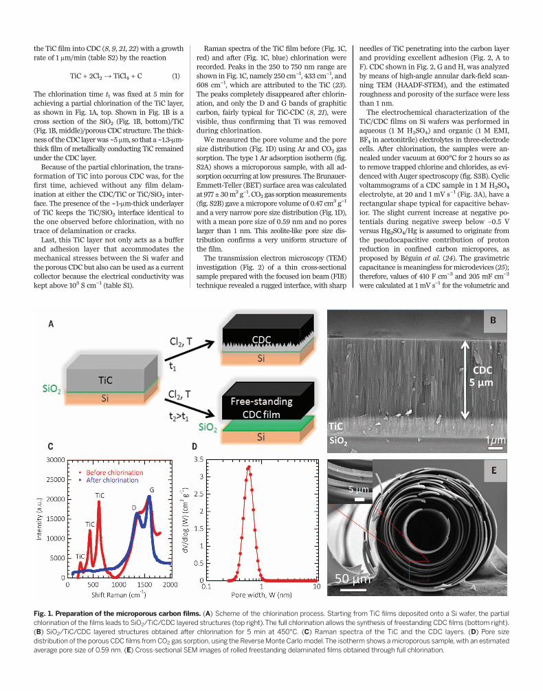
The chlorination time t1 was fixed at 5 min forachieving a partial chlorination of the TiC layer,as shown in Fig. 1A, top. Shown in Fig. 1B is across section of the SiO2 (Fig. 1B, bottom)/TiC(Fig. 1B,middle)/porous CDC structure. The thick-ness of theCDC layerwas~5 mm, so that a~1.3-mm-thick film of metallically conducting TiC remainedunder the CDC layer.Because of the partial chlorination, the trans-
formation of TiC into porous CDC was, for thefirst time, achieved without any film delam-ination at either the CDC/TiC or TiC/SiO2 inter-face. The presence of the ~1-mm-thick underlayerof TiC keeps the TiC/SiO2 interface identical tothe one observed before chlorination, with notrace of delamination or cracks.Last, this TiC layer not only acts as a buffer
and adhesion layer that accommodates themechanical stresses between the Si wafer andthe porous CDC but also can be used as a currentcollector because the electrical conductivity waskept above 103 S cm−1 (table S1).
Raman spectra of the TiC film before (Fig. 1C,red) and after (Fig. 1C, blue) chlorination wererecorded. Peaks in the 250 to 750 nm range areshown in Fig. 1C, namely 250 cm−1, 433 cm−1, and608 cm−1, which are attributed to the TiC (23).The peaks completely disappeared after chlorin-ation, and only the D and G bands of graphiticcarbon, fairly typical for TiC-CDC (8, 21), werevisible, thus confirming that Ti was removedduring chlorination.We measured the pore volume and the pore
size distribution (Fig. 1D) using Ar and CO2 gassorption. The type 1 Ar adsorption isotherm (fig.S2A) shows a microporous sample, with all ad-sorption occurring at low pressures. The Brunauer-Emmett-Teller (BET) surface area was calculatedat 977 ± 30m2 g−1. CO2 gas sorptionmeasurements(fig. S2B) gave amicropore volume of 0.47 cm3 g−1
and a very narrow pore size distribution (Fig. 1D),with a mean pore size of 0.59 nm and no poreslarger than 1 nm. This zeolite-like pore size dis-tribution confirms a very uniform structure ofthe film.The transmission electron microscopy (TEM)
investigation (Fig. 2) of a thin cross-sectionalsample prepared with the focused ion beam (FIB)technique revealed a rugged interface, with sharp
needles of TiC penetrating into the carbon layerand providing excellent adhesion (Fig. 2, A toF). CDC shown in Fig. 2, G and H, was analyzedby means of high-angle annular dark-field scan-ning TEM (HAADF-STEM), and the estimatedroughness and porosity of the surface were lessthan 1 nm.The electrochemical characterization of the
TiC/CDC films on Si wafers was performed inaqueous (1 M H2SO4) and organic (1 M EMI,BF4 in acetonitrile) electrolytes in three-electrodecells. After chlorination, the samples were an-nealed under vacuum at 600°C for 2 hours so asto remove trapped chlorine and chlorides, as evi-denced with Auger spectroscopy (fig. S3B). Cyclicvoltammograms of a CDC sample in 1 M H2SO4
electrolyte, at 20 and 1 mV s−1 (Fig. 3A), have arectangular shape typical for capacitive behav-ior. The slight current increase at negative po-tentials during negative sweep below –0.5 Vversus Hg2SO4/Hg is assumed to originate fromthe pseudocapacitive contribution of protonreduction in confined carbon micropores, asproposed by Béguin et al. (24). The gravimetriccapacitance ismeaningless formicrodevices (25);therefore, values of 410 F cm−3 and 205 mF cm−2
were calculated at 1 mV s−1 for the volumetric and
Fig. 1. Preparation of the microporous carbon films. (A) Scheme of the chlorination process. Starting from TiC films deposited onto a Si wafer, the partialchlorination of the films leads to SiO2/TiC/CDC layered structures (top right).The full chlorination allows the synthesis of freestanding CDC films (bottom right).(B) SiO2/TiC/CDC layered structures obtained after chlorination for 5 min at 450°C. (C) Raman spectra of the TiC and the CDC layers. (D) Pore sizedistribution of the porous CDC films fromCO2 gas sorption, using the ReverseMonte Carlo model.The isotherm shows amicroporous sample,with an estimatedaverage pore size of 0.59 nm. (E) Cross-sectional SEM images of rolled freestanding delaminated films obtained through full chlorination.

areal capacitance, respectively. Cyclic voltam-metry at low scan rates provides evidence of alow-leakage current in the cell. The electrodecapacitance was stable over 10,000 cycles (Fig. 3B).The change of the normalized capacitance versusthe potential scan rate provides evidence for thehigh power capability of these films (Fig. 3B, inset)as more than 200 F cm−3 (100 mF cm−2) were stilldelivered during 0.9 s discharge (1 V s−1), whichoutperforms the current state of the art ofcarbon-based double-layer capacitors andmicro-supercapacitors (26–30).The cyclic voltammogram (CV) of a Si/TiC/
CDC film annealed at 600°C in hydrogen andtested as a single electrode at 20 mV s−1 in 1 MEMI,BF4 in acetonitrile electrolyte shows a typi-cal capacitive behavior within a potential win-dow limited to 2.0 V (fig. S3D). The volumetriccapacitance of the sample reached 170 F cm−3,which is in line with the data reported for TiC-CDC films (8). Annealing at 600°C under H2
atmosphere opens carbon pores (22), thus im-proving accessibility to large EMI+ ions comparedwith that of a nonannealed sample (fig. S3C)without affecting the adherence at the CDC/TiCinterface. CDC pore size, which determines ca-pacitance, can be controlled with the synthesistemperature (8, 21, 22). Shown in Fig. 3C areCVs of a 2.2-mm-thick CDC film on a Si/TiC/CDCelectrode prepared through partial chlorinationat 700°C for 30 s, obtained at different rates.CVs show a typical capacitive behavior within apotential window up to 3 V, resulting in an im-provement of the energy andpower density (Fig. 4)and the volumetric capacitance reaching 160 Fcm−3 at 20 mV s−1.Following the electrochemical characteriza-
tions of the CDC films, two-electrode micro-supercapacitor devices were manufactured andcharacterized. Micro-supercapacitors containingnine fingers per polarity (2 mm long, 100 mmwide,with 15 mm separation) (Fig. 3D) were prepared
according to the different steps detailed in figs.S4 and S5, A to C. A picture of a 7.62-cm Si wafercontaining 40 patterned micro-supercapacitorsis shown in Fig. 3E, thus confirming that theprocess can be easily scalable. Ti/Au film wasevaporated on both sides of the large pad forensuring electrical contact. The CVs of a micro-supercapacitor in H2SO4 1 M electrolyte arepresented in Fig. 3F. In this example, the chlo-rination of a 3.5-mm-thick patterned TiC layerled to formation of a 1.4-mm-thick CDC film.The electrode volumetric capacitance reached350 F cm−3, which is in line with the electro-chemical performance of three-electrode cellspresented in Fig. 3A. The slight decrease of thevolumetric capacitance compared with that of asingle electrode (410 F cm−3) may originate fromvery small separation (only 15 mm) between theelectrode fingers. The capacitance change withthe potential scan rate is shown in fig. S5D; theinitial capacitance is 350 F cm−3. More than 50%
Fig. 2. Structural characterization of the SiO2/TiC/CDC electrodes.(A) Selected-area electron diffraction (SAED) pattern of TiC [(C), blue square]showing the cubic structure. (B) SAED pattern of CDC [(C), green square],showing an amorphous structure. (C) TEM image of the TiC/CDC interface,withthe areas for the SAED analysis [blue and green squares in (A) and (B), re-spectively]. (D) Energy-dispersive x-ray analysis showing the absence of Ti
in the carbon film. (E) Bright-field STEM image of the interface, showing theinterpenetration of TiC and carbon structures, which proves the excellent ad-hesion between the layers. (F) High-resolution TEM image showing the crys-tallographic orientation of the TiC cubic structure. (G) HAADF-STEM image ofthe amorphous carbon and (H) roughness of the CDC surface, which is es-timated to be less than 1 nm (scanned area, 10 by 10 nm).
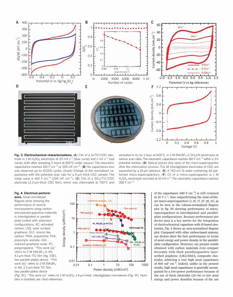
of the capacitance (180 F cm−3) is still retainedat 10 V s−1, thus outperforming the state-of-the-art micro-supercapacitors (1, 16, 17, 27, 29, 31), ascan be seen in the volume-normalized Ragoneplot in fig. S6 showing performance of micro-supercapacitors in interdigitated and parallel-plate configurations. Because performance perdevice area is a key metric for the integrationof electrochemical capacitors with Si-based elec-tronics, Fig. 4 shows an area-normalized Ragoneplot. Compared with other carbon-based systems,our devices show the best performance in termsof areal energy and power density in the parallel-plate configuration. Moreover, our present resultsobtained with carbon materials even comparefavorably with thick pseudocapacitive laser-scribed graphene (LSG)/MnO2 composite elec-trodes, achieving a very high areal capacitanceof 800 mF cm–2. Indeed, unlike in the presentresults, high areal capacitance is generally accom-panied by a low-power performance because ofthe use of thick electrodes (32–34) or low arealenergy and power densities because of the use
Fig. 3. Electrochemical characterizations. (A) CVs of a Si/TiC/CDC elec-trode in 1 M H2SO4 electrolyte at 20 mV s−1 (blue curve) and 1 mV s−1 (redcurve), both after annealing 2 hours at 600°C under vacuum. The volumetriccapacitance reaches 410 F cm−3 or 205 mF cm−2. (B) No capacitance losswas observed up to 10,000 cycles. (Inset) Change of the normalized ca-pacitance with the potential scan rate for a 5-mm-thick CDC sample. Theinitial value is 410 F cm−3 (205 mF cm−2). (C) CVs of a SiO2/TiC/CDCelectrode (2.2-mm-thick CDC film), which was chlorinated at 700°C and
annealed in H2 for 1 hour at 600°C, in 2 M EMI,BF4 in CH3CN electrolyte atvarious scan rates. The volumetric capacitance reaches 160 F cm−3 within a 3-Vpotential window. (D) Optical picture (top view) of the micro-supercapacitorafter the chlorination process. The 18 interdigitated electrodes of CDC areseparated by a 15-mm distance. (E) A 7.62-cm Si wafer containing 40 pat-terned micro-supercapacitors. (F) CV of a micro-supercapacitor in 1 MH2SO4 electrolyte recorded at 10 mV s−1. The volumetric capacitance reaches350 F cm−3.
Fig. 4. Electrical perform-ance. Areal-normalizedRagone plots showing theperformance of severalmicrosystems using carbonand pseudocapacitive materialsin interdigitated or parallel-plate (noted with asterisks)configurations. AC, activatedcarbon; LSG, laser scribedgraphene; OLC, onions likecarbon; PANI, polyaniline; PVA,polyvinylic acetate; rGO,reduced graphene oxide; PC,polypropylene. “This work (a)”refers to 2 M EMI,BF4 in AN,4.1-mm-thick TiC film (fig. S3E),two parallel plates device. “Thiswork (b)” refers to 2 M EMI,BF4in AN, 2.2-mm-thick TiC film,two parallel plates device(Fig. 3C). “This work (c)” refers to 1 M H2SO4, 1.4-mm-thick, interdigitated microdevice (Fig. 3F). Num-bers in brackets are cited references.
of faradic materials with a narrow operating po-tential window (13).Themechanical properties of the films reported
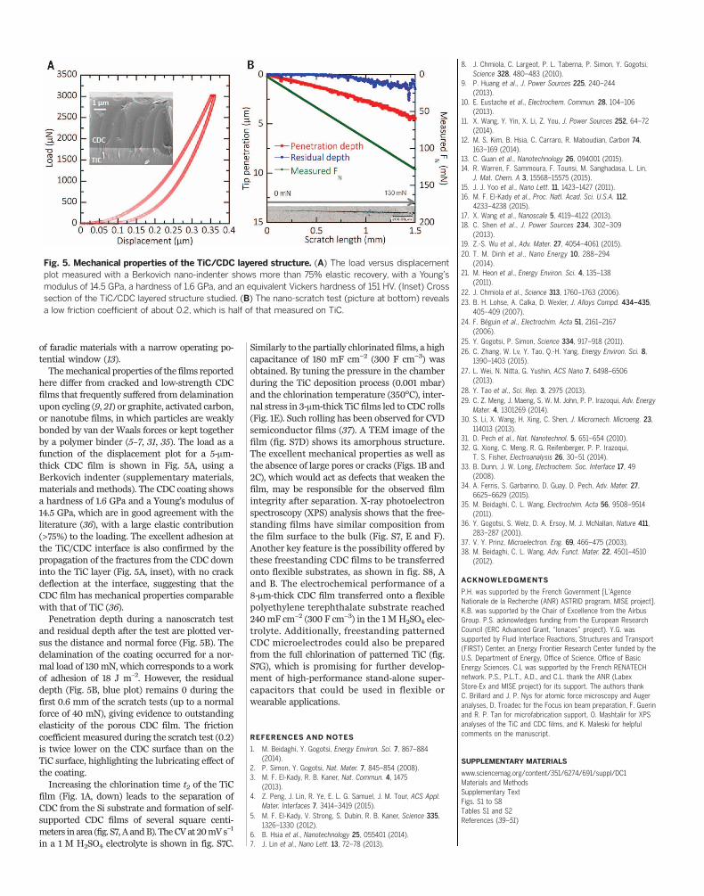
here differ from cracked and low-strength CDCfilms that frequently suffered from delaminationupon cycling (9, 21) or graphite, activated carbon,or nanotube films, in which particles are weaklybonded by van der Waals forces or kept togetherby a polymer binder (5–7, 31, 35). The load as afunction of the displacement plot for a 5-mm-thick CDC film is shown in Fig. 5A, using aBerkovich indenter (supplementary materials,materials and methods). The CDC coating showsa hardness of 1.6 GPa and a Young’s modulus of14.5 GPa, which are in good agreement with theliterature (36), with a large elastic contribution(>75%) to the loading. The excellent adhesion atthe TiC/CDC interface is also confirmed by thepropagation of the fractures from the CDC downinto the TiC layer (Fig. 5A, inset), with no crackdeflection at the interface, suggesting that theCDC film has mechanical properties comparablewith that of TiC (36).Penetration depth during a nanoscratch test
and residual depth after the test are plotted ver-sus the distance and normal force (Fig. 5B). Thedelamination of the coating occurred for a nor-mal load of 130 mN, which corresponds to a workof adhesion of 18 J m–2. However, the residualdepth (Fig. 5B, blue plot) remains 0 during thefirst 0.6 mm of the scratch tests (up to a normalforce of 40 mN), giving evidence to outstandingelasticity of the porous CDC film. The frictioncoefficient measured during the scratch test (0.2)is twice lower on the CDC surface than on theTiC surface, highlighting the lubricating effect ofthe coating.Increasing the chlorination time t2 of the TiC
film (Fig. 1A, down) leads to the separation ofCDC from the Si substrate and formation of self-supported CDC films of several square centi-meters in area (fig. S7, A andB). TheCVat 20mVs−1
in a 1 M H2SO4 electrolyte is shown in fig. S7C.
Similarly to the partially chlorinated films, a highcapacitance of 180 mF cm−2 (300 F cm−3) wasobtained. By tuning the pressure in the chamberduring the TiC deposition process (0.001 mbar)and the chlorination temperature (350°C), inter-nal stress in 3-mm-thick TiC films led to CDC rolls(Fig. 1E). Such rolling has been observed for CVDsemiconductor films (37). A TEM image of thefilm (fig. S7D) shows its amorphous structure.The excellent mechanical properties as well asthe absence of large pores or cracks (Figs. 1B and2C), which would act as defects that weaken thefilm, may be responsible for the observed filmintegrity after separation. X-ray photoelectronspectroscopy (XPS) analysis shows that the free-standing films have similar composition fromthe film surface to the bulk (Fig. S7, E and F).Another key feature is the possibility offered bythese freestanding CDC films to be transferredonto flexible substrates, as shown in fig. S8, Aand B. The electrochemical performance of a8-mm-thick CDC film transferred onto a flexiblepolyethylene terephthalate substrate reached240mF cm−2 (300 F cm−3) in the 1 MH2SO4 elec-trolyte. Additionally, freestanding patternedCDC microelectrodes could also be preparedfrom the full chlorination of patterned TiC (fig.S7G), which is promising for further develop-ment of high-performance stand-alone super-capacitors that could be used in flexible orwearable applications.
REFERENCES AND NOTES
1. M. Beidaghi, Y. Gogotsi, Energy Environ. Sci. 7, 867–884(2014).
2. P. Simon, Y. Gogotsi, Nat. Mater. 7, 845–854 (2008).3. M. F. El-Kady, R. B. Kaner, Nat. Commun. 4, 1475
(2013).4. Z. Peng, J. Lin, R. Ye, E. L. G. Samuel, J. M. Tour, ACS Appl.
Mater. Interfaces 7, 3414–3419 (2015).5. M. F. El-Kady, V. Strong, S. Dubin, R. B. Kaner, Science 335,
1326–1330 (2012).6. B. Hsia et al., Nanotechnology 25, 055401 (2014).7. J. Lin et al., Nano Lett. 13, 72–78 (2013).
8. J. Chmiola, C. Largeot, P. L. Taberna, P. Simon, Y. Gogotsi,Science 328, 480–483 (2010).
9. P. Huang et al., J. Power Sources 225, 240–244(2013).
10. E. Eustache et al., Electrochem. Commun. 28, 104–106(2013).
11. X. Wang, Y. Yin, X. Li, Z. You, J. Power Sources 252, 64–72(2014).
12. M. S. Kim, B. Hsia, C. Carraro, R. Maboudian, Carbon 74,163–169 (2014).
13. C. Guan et al., Nanotechnology 26, 094001 (2015).14. R. Warren, F. Sammoura, F. Tounsi, M. Sanghadasa, L. Lin,
J. Mat. Chem. A 3, 15568–15575 (2015).15. J. J. Yoo et al., Nano Lett. 11, 1423–1427 (2011).16. M. F. El-Kady et al., Proc. Natl. Acad. Sci. U.S.A. 112,
4233–4238 (2015).17. X. Wang et al., Nanoscale 5, 4119–4122 (2013).18. C. Shen et al., J. Power Sources 234, 302–309
(2013).19. Z.-S. Wu et al., Adv. Mater. 27, 4054–4061 (2015).20. T. M. Dinh et al., Nano Energy 10, 288–294
(2014).21. M. Heon et al., Energy Environ. Sci. 4, 135–138
(2011).22. J. Chmiola et al., Science 313, 1760–1763 (2006).23. B. H. Lohse, A. Calka, D. Wexler, J. Alloys Compd. 434–435,
405–409 (2007).24. F. Béguin et al., Electrochim. Acta 51, 2161–2167
(2006).25. Y. Gogotsi, P. Simon, Science 334, 917–918 (2011).26. C. Zhang, W. Lv, Y. Tao, Q.-H. Yang, Energy Environ. Sci. 8,
1390–1403 (2015).27. L. Wei, N. Nitta, G. Yushin, ACS Nano 7, 6498–6506
(2013).28. Y. Tao et al., Sci. Rep. 3, 2975 (2013).29. C. Z. Meng, J. Maeng, S. W. M. John, P. P. Irazoqui, Adv. Energy
Mater. 4, 1301269 (2014).30. S. Li, X. Wang, H. Xing, C. Shen, J. Micromech. Microeng. 23,
114013 (2013).31. D. Pech et al., Nat. Nanotechnol. 5, 651–654 (2010).32. G. Xiong, C. Meng, R. G. Reifenberger, P. P. Irazoqui,
T. S. Fisher, Electroanalysis 26, 30–51 (2014).33. B. Dunn, J. W. Long, Electrochem. Soc. Interface 17, 49
(2008).34. A. Ferris, S. Garbarino, D. Guay, D. Pech, Adv. Mater. 27,
6625–6629 (2015).35. M. Beidaghi, C. L. Wang, Electrochim. Acta 56, 9508–9514
(2011).36. Y. Gogotsi, S. Welz, D. A. Ersoy, M. J. McNallan, Nature 411,
283–287 (2001).37. V. Y. Prinz, Microelectron. Eng. 69, 466–475 (2003).38. M. Beidaghi, C. L. Wang, Adv. Funct. Mater. 22, 4501–4510
(2012).
ACKNOWLEDGMENTS
P.H. was supported by the French Government [L’AgenceNationale de la Recherche (ANR) ASTRID program, MISE project].K.B. was supported by the Chair of Excellence from the AirbusGroup. P.S. acknowledges funding from the European ResearchCouncil (ERC Advanced Grant, “Ionaces” project). Y.G. wassupported by Fluid Interface Reactions, Structures and Transport(FIRST) Center, an Energy Frontier Research Center funded by theU.S. Department of Energy, Office of Science, Office of BasicEnergy Sciences. C.L was supported by the French RENATECHnetwork. P.S., P.L.T., A.D., and C.L. thank the ANR (LabexStore-Ex and MISE project) for its support. The authors thankC. Brillard and J. P. Nys for atomic force microscopy and Augeranalyses, D. Troadec for the Focus ion beam preparation, F. Guerinand R. P. Tan for microfabrication support, O. Mashtalir for XPSanalyses of the TiC and CDC films, and K. Maleski for helpfulcomments on the manuscript.
SUPPLEMENTARY MATERIALS
www.sciencemag.org/content/351/6274/691/suppl/DC1Materials and MethodsSupplementary TextFigs. S1 to S8Tables S1 and S2References (39–51)
Fig. 5. Mechanical properties of the TiC/CDC layered structure. (A) The load versus displacementplot measured with a Berkovich nano-indenter shows more than 75% elastic recovery, with a Young’smodulus of 14.5 GPa, a hardness of 1.6 GPa, and an equivalent Vickers hardness of 151 HV. (Inset) Crosssection of the TiC/CDC layered structure studied. (B) The nano-scratch test (picture at bottom) revealsa low friction coefficient of about 0.2, which is half of that measured on TiC.


![Transparent and Freestanding Single‐Walled Carbon …carbon nanotubes (CNTs),[2–4] graphene,[5]flexible transparent conductive films (TCFs). Here, inspired by the extrusion metal](https://img.pdfslide.net/doc/110x75/60af0258efb48311be6f6a13/transparent-and-freestanding-singleawalled-carbon-carbon-nanotubes-cnts2a4.jpg)