Embed Size (px)
Citation preview

Freescale SemiconductorApplication Note
Document Number: AN3305Rev. 1, 02/2007
Contents
Introduction . . . . . . . . . . . . . . . . . . . . . . . . . . . . . . . . . . . 1On-Chip Solutions . . . . . . . . . . . . . . . . . . . . . . . . . . . . . . 2
2.1 Low-Voltage Detect (LVD) System . . . . . . . . . . . . . 22.2 Illegal Op-Code and Illegal Address Resets . . . . . . 52.3 Clock Source System Protection. . . . . . . . . . . . . . . 52.4 Nonvolatile Memory Protection . . . . . . . . . . . . . . . 102.5 Computer-Operating Properly (COP) Watchdog. . 12Additional System Protection Techniques . . . . . . . . . . . 15
3.1 Filling Unused Memory . . . . . . . . . . . . . . . . . . . . . 153.2 Monitoring the Bus Clock Frequency. . . . . . . . . . . 183.3 LVD Checks Using the ADC Module . . . . . . . . . . . 193.4 Additional Protection Methods. . . . . . . . . . . . . . . . 20Application Example: Brownout Protection . . . . . . . . . . 21
4.1 Hardware Configuration. . . . . . . . . . . . . . . . . . . . . 214.2 Software Configuration . . . . . . . . . . . . . . . . . . . . . 22
5 Conclusion. . . . . . . . . . . . . . . . . . . . . . . . . . . . . . . . . . . 246 References . . . . . . . . . . . . . . . . . . . . . . . . . . . . . . . . . . 24
On-Chip System Protection Basics for HCS08 Microcontrollersby: Christine Peng8-Bit Systems and Applications EngineeringAustin, Texas
1 IntroductionMicrocontrollers occasionally operate outside of specification because of adverse effects due to electromagnetic interference, noise transients, temperature, variations in voltage, power-supply conditions, and frequency. Faulty software design in combination with these external influences can cause code runaway, memory corruption, unstable clock activity, and other undefined behaviors. Additionally, inadequate security can lead to hacked application software, resulting in the loss of customer confidence and millions of dollars. To prevent faults and unwanted behavior in applications where system protection is critical, the HCS08 family of microcontrollers includes many system-protection features.
This application note’s purpose is to introduce these features and to explain how to use them in HCS08 MCU applications. Focus will be on system-protection solutions available on-chip only. Detailed information on external hardware-design techniques for transient
12
3
4
© Freescale Semiconductor, Inc., 2006. All rights reserved.
On-Chip Solutions
immunity protection and layout techniques for noise reduction are available in AN2764 and AN1259, respectively. Although this application note discusses 5 V automotive HCS08 microcontrollers, much of this information is useful for consumer and industrial electronics as well.
2 On-Chip SolutionsThe HCS08 range of MCUs includes a variety of on-chip solutions to help prevent system malfunction and to ensure application security. The solutions discussed in this application note include:
• Low-Voltage Detect (LVD) System• Illegal Op-code and Illegal Address Resets• Clock Source System Protection• Flash Protection and Security• Computer Operating Properly (COP) Watchdog
2.1 Low-Voltage Detect (LVD) SystemBecause supply voltage variations and low voltage (brownout) can cause a variety of problems for MCU applications, HCS08 microcontrollers include an LVD system to guard against low-voltage conditions. The LVD system allows the MCU to sense a drop in supply voltage and then shut itself down in a well-defined manner to protect memory contents and control MCU system states during these variations.
2.1.1 Features
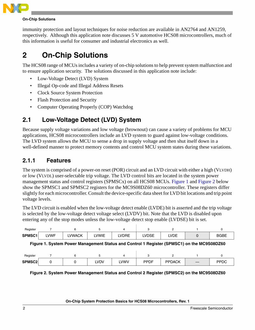
The system is comprised of a power-on reset (POR) circuit and an LVD circuit with either a high (VLVDH) or low (VLVDL) user-selectable trip voltage. The LVD control bits are located in the system power management status and control registers (SPMSCx) on all HCS08 MCUs. Figure 1 and Figure 2 below show the SPMSC1 and SPMSC2 registers for the MC9S08DZ60 microcontroller. These registers differ slightly for each microcontroller. Consult the device-specific data sheet for LVD bit locations and trip point voltage levels.
The LVD circuit is enabled when the low-voltage detect enable (LVDE) bit is asserted and the trip voltage is selected by the low-voltage detect voltage select (LVDV) bit. Note that the LVD is disabled upon entering any of the stop modes unless the low-voltage detect stop enable (LVDSE) bit is set.
Figure 1. System Power Management Status and Control 1 Register (SPMSC1) on the MC9S08DZ60
Figure 2. System Power Management Status and Control 2 Register (SPMSC2) on the MC9S08DZ60
Register 7 6 5 4 3 2 1 0
SPMSC1 LVWF LVWACK LVWIE LVDRE LVDSE LVDE 0 BGBE
Register 7 6 5 4 3 2 1 0
SPMSC2 0 0 LVDV LVWV PPDF PPDACK — PPDC
On-Chip System Protection Basics for HCS08 Microcontrollers, Rev. 1
Freescale Semiconductor2
On-Chip Solutions
2.1.1.1 LVD Power-On Reset Operation
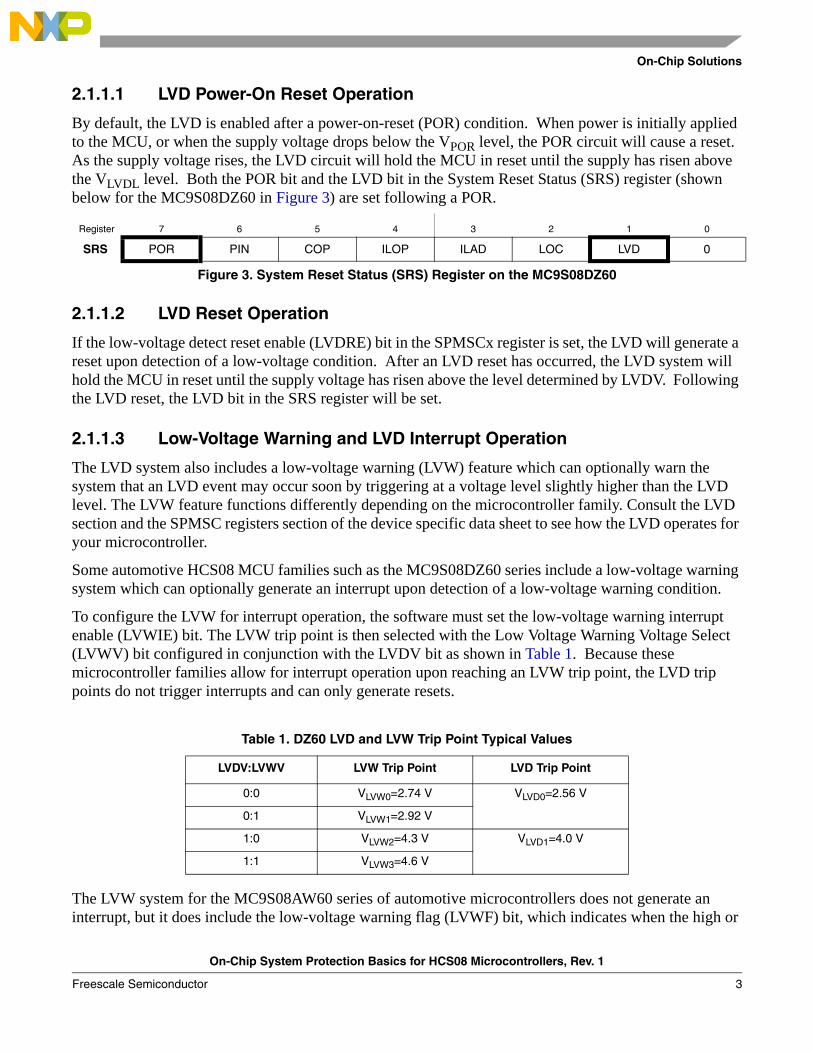
By default, the LVD is enabled after a power-on-reset (POR) condition. When power is initially applied to the MCU, or when the supply voltage drops below the VPOR level, the POR circuit will cause a reset. As the supply voltage rises, the LVD circuit will hold the MCU in reset until the supply has risen above the VLVDL level. Both the POR bit and the LVD bit in the System Reset Status (SRS) register (shown below for the MC9S08DZ60 in Figure 3) are set following a POR.
Figure 3. System Reset Status (SRS) Register on the MC9S08DZ60
2.1.1.2 LVD Reset Operation
If the low-voltage detect reset enable (LVDRE) bit in the SPMSCx register is set, the LVD will generate a reset upon detection of a low-voltage condition. After an LVD reset has occurred, the LVD system will hold the MCU in reset until the supply voltage has risen above the level determined by LVDV. Following the LVD reset, the LVD bit in the SRS register will be set.
2.1.1.3 Low-Voltage Warning and LVD Interrupt Operation
The LVD system also includes a low-voltage warning (LVW) feature which can optionally warn the system that an LVD event may occur soon by triggering at a voltage level slightly higher than the LVD level. The LVW feature functions differently depending on the microcontroller family. Consult the LVD section and the SPMSC registers section of the device specific data sheet to see how the LVD operates for your microcontroller.
Some automotive HCS08 MCU families such as the MC9S08DZ60 series include a low-voltage warning system which can optionally generate an interrupt upon detection of a low-voltage warning condition.
To configure the LVW for interrupt operation, the software must set the low-voltage warning interrupt enable (LVWIE) bit. The LVW trip point is then selected with the Low Voltage Warning Voltage Select (LVWV) bit configured in conjunction with the LVDV bit as shown in Table 1. Because these microcontroller families allow for interrupt operation upon reaching an LVW trip point, the LVD trip points do not trigger interrupts and can only generate resets.
The LVW system for the MC9S08AW60 series of automotive microcontrollers does not generate an interrupt, but it does include the low-voltage warning flag (LVWF) bit, which indicates when the high or
Register 7 6 5 4 3 2 1 0
SRS POR PIN COP ILOP ILAD LOC LVD 0
Table 1. DZ60 LVD and LVW Trip Point Typical Values
LVDV:LVWV LVW Trip Point LVD Trip Point
0:0 VLVW0=2.74 V VLVD0=2.56 V
0:1 VLVW1=2.92 V
1:0 VLVW2=4.3 V VLVD1=4.0 V
1:1 VLVW3=4.6 V
On-Chip System Protection Basics for HCS08 Microcontrollers, Rev. 1
Freescale Semiconductor 3
On-Chip Solutions
low-trip voltage selected by the LVWV bit has been reached. Unlike the MC9S08DZ60 series, on the MC9S08AW60 MCU, the LVWV bit operates independently from the LVDV bit.
The LVD system on the MC9S08AW60 MCU family also allows for an interrupt upon detection of the low voltage trigger point selected by LVDV. To configure the LVD for interrupt operation, the software must set the low-voltage detect interrupt enable (LVDIE) bit in addition to the LVDE bit. The LVDRE bit must also be clear in order for LVD interrupts to occur on the MC9S08AW60.
2.1.1.3.1 Usage
The purpose for the LVD interrupt and warning feature is to give the software the ability to save important variables to nonvolatile memory and to shut down peripherals safely before power is lost. Because on the MC9S08DZ60 series, the low-voltage warning trip points are above the low-voltage detect trip points, the low-voltage warning interrupt gives the software time to perform safe system shutdown procedures before either the LVD reset trip point is reached or the system loses power.
Note that if LVW interrupts are enabled and the computer operating properly (COP) feature is used, the LVW interrupt service routine containing the low voltage shutdown sequence may be interrupted by a COP reset. This is because, in the event that the supply voltage drops below the LVW trip point, the LVW interrupt will trigger continuously, preventing the main loop from servicing the COP. Therefore, the COP will time out and reset the MCU unexpectedly. More information on the COP can be found in Section 2.5, “Computer-Operating Properly (COP) Watchdog.”
On the other hand, software written for the MC9S08AW60 family can use the LVW flag feature with the LVD interrupt or reset options in combinations that best suit the application. On the MC9S08AW60 series, the high and low LVW trip voltages (VLVWH and VLVWL) are equal to the high and low LVD trip voltages (VLVDH and VLVDL). Unlike the previously mentioned MCU families, the LVW levels are not higher than the LVD levels; therefore, the LVD system on the MC9S08AW60 family must be configured differently.
Some example combinations for the MC9S08AW60 family configure the LVD such that:1. LVWV = 1 and LVDV = 0 with LVDRE = 1 to trigger the LVWF flag at the high LVD/LVW trip
point, giving the system software time to run through a safe shut-down sequence in the main program loop before the low LVD trip point resets the MCU.
2. LVDV = 1, LVDRE = 0, and LVDIE = 1 to trigger an interrupt at the high LVD trip point, giving the system software ample time to run through a safe shut-down sequence in an interrupt service routine before the system reaches the POR level/shuts down.
In the interrupt service routine or LVW safe shut-down sequence, it is generally good practice to perform at least one or some of the following:
1. Save critical data and register states to internal or external nonvolatile memory, such as flash or EEPROM. Note that this is possible only if there is enough time in a powered state before the voltage falls below specification for writing to nonvolatile memory. Using a large capacitor on the power supply line to prevent rapid power decay can buy the system some time. If possible, safely shut down peripherals and put port pins into a desired state.
2. Put the part into a low-power stop mode to minimize current consumption so that all peripherals and port pins are in a “safe” state upon power loss.
On-Chip System Protection Basics for HCS08 Microcontrollers, Rev. 1
Freescale Semiconductor4
On-Chip Solutions
3. Safely shut down peripherals to put the peripherals in a stable known state with the least amount of activity.
A code example for LVD system initialization and the corresponding interrupt service routine on the MC9S08DZ60 is included in the software that accompanies this application note. This document also includes an alternative method of implementing an LVD system in Section 3.3, “LVD Checks Using the ADC Module,” for users who want to designate their own LVD trip point levels.
2.2 Illegal Op-Code and Illegal Address ResetsIn the event of faulty coding or disrupted software execution flow due to a disturbance, all HCS08 microcontrollers include on-chip features to generate a system reset, which will then restore normal MCU operation. The illegal op-code (ILOP) bit in the System Reset Status (SRS) register will generate a reset upon detection of an illegal op-code. For example, the STOP instruction is considered illegal if stop is disabled by STOPE=0. Likewise, the BGND instruction is considered illegal if active background mode is disabled by ENBDM = 0. The ILOP reset can also be used strategically for system protection to handle code runaway. This will be discussed in more detail in Section 3.1, “Filling Unused Memory.”
Some HCS08 microcontrollers like the MC9S08DZ60 series include an illegal-address (ILAD) bit in the SRS register which will generate a reset upon an attempt by user software to access either data or an instruction at an unimplemented memory address. For example, if a section of unimplemented memory is on a device between locations 0x0C80 and 0x14FF and the software attempts to access location 0x1000, the setting of the ILAD bit will reset the MCU.
2.3 Clock Source System ProtectionCurrent HCS08 microcontrollers include one of three different clock modules to generate the system bus frequency: the internal clock generator (ICG) module, the internal clock source (ICS) module, and the multi-purpose clock generator (MCG) module. All modules can use either an internal system clock (cost-effective clocking solution) or an external clock source to generate the bus clock. Because oscillator circuits are sensitive to EMC, careful consideration should be taken when selecting and laying out all external components. This is discussed in detail in a different application note, AN2764, Transient Immunity. In the event that despite all external oscillator protection loss of clock or lock still occurs, all HCS08 clock modules include built-in features to handle clocking glitches or failures. This section will describe the clock monitor features available on the HCS08 MCU families to protect the system in the event of loss of lock or clock. Table 2 below summarizes the clock-source protection options available for each of the three clock modules available for HCS08 microcontrollers.
Table 2. Clock-Source Protection Options
Clock Modes Loss of lock Loss of clock
ICG Interrupt or Reset Reset or Clock Switching
ICS N/A N/A
MCG Interrupt Reset
On-Chip System Protection Basics for HCS08 Microcontrollers, Rev. 1
Freescale Semiconductor 5
On-Chip Solutions
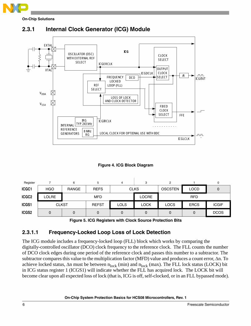
2.3.1 Internal Clock Generator (ICG) Module
Figure 4. ICG Block Diagram
Figure 5. ICG Registers with Clock Source Protection Bits
2.3.1.1 Frequency-Locked Loop Loss of Lock Detection
The ICG module includes a frequency-locked loop (FLL) block which works by comparing the digitally-controlled oscillator (DCO) clock frequency to the reference clock. The FLL counts the number of DCO clock edges during one period of the reference clock and passes this number to a subtractor. The subtractor compares this value to the multiplication factor (MFD) value and produces a count error, Δn. To achieve locked status, Δn must be between nlock (min) and nlock (max). The FLL lock status (LOCK) bit in ICG status register 1 (ICGS1) will indicate whether the FLL has acquired lock. The LOCK bit will become clear upon all expected loss of lock (that is, ICG is off, self-clocked, or in an FLL bypassed mode).
Register 7 6 5 4 3 2 1 0
ICGC1 HGO RANGE REFS CLKS OSCSTEN LOCD 0
ICGC2 LOLRE MFD LOCRE RFD
ICGS1 CLKST REFST LOLS LOCK LOCS ERCS ICGIF
ICGS2 0 0 0 0 0 0 0 DCOS
OSCILLATOR (OSC)
FREQUENCY
INTERNAL
EXTAL
XTAL
REFERENCE GENERATORS
CLOCKSELECT
8 MHz
IRG
LOSS OF LOCKAND CLOCK DETECTOR
LOCKEDLOOP (FLL)
FIXEDCLOCK
SELECT
ICGOUT
TYP 243 kHz
RGICGLCLK
ICG
FFE
VDDA
VSSA
DCO
WITH EXTERNAL REFSELECT
REFSELECT
LOCAL CLOCK FOR OPTIONAL USE WITH BDC
OUTPUTCLOCK
SELECT ICGDCLK /R
ICGERCLK
ICGIRCLK
On-Chip System Protection Basics for HCS08 Microcontrollers, Rev. 1
Freescale Semiconductor6

On-Chip Solutions
After the FLL has locked, Δn must stay between nunlock (min) and nunlock (max) to remain locked. If Δn goes outside this range unexpectedly, the loss of lock status (LOLS) bit in ICGS1 is set and remains set until cleared by software or until the MCU is reset. The LOLS bit is a sticky indication of only unexpected loss-of-lock conditions and will not be triggered by expected loss-of-lock.
In the event of loss of FLL lock, the ICG can generate either an interrupt or a reset by using the loss of lock reset enable (LOLRE) bit in ICG control register 2 (ICGC2). If an interrupt is requested upon loss of lock, the software can choose to handle the loss of lock however the programmer chooses, but in most cases, the software will loop in the service routine until lock is reengaged. The LOLS bit should also be cleared here by reading the status register then writing a 1 to the ICG interrupt flag (ICGIF) bit in ICGS1.
2.3.1.2 Loss-of-Clock Detection
The ICG module includes a clock monitor system which monitors both the digitally-controlled oscillator (DCO) and the external reference clock for loss of clock events. The DCO clock stable (DCOS) bit in ICGS2 monitors when the DCO clock is stable, meaning the count error has not changed by more than nunlock for two consecutive samples and the DCO clock is not static. The bit is cleared (indicating an unstable DCO clock) upon entering the off state. The external reference clock status (ERCS) bit in ICGS1 is an indication of whether or not the external reference clock (ICGERCLK) meets the minimum frequency requirement. Through the monitor system, the module allows for automatic clock switching to a bypassed mode or to an internal clock reference upon loss of clock. See Table 3 for the results of mode switching upon loss of clock.
If the ICG is in FLL-bypassed, external (FBE) mode, a loss of external reference clock will cause the ICG to enter self-clocked mode (SCM). The filter bits will maintain ICGDCLK and, therefore, ICGOUT at its previous frequency. The FLL and, therefore, the DCO clock is not used in FBE mode.
If the ICG is in FLL-engaged, external (FEE) mode, a loss of the external reference clock causes the ICG to enter SCM with the fICGDCLK and, therefore, fICGOUT maintain at their previous frequencies. If the external reference clock signal was lost in FEE unlocked mode, fICGOUT will double instead of maintain. A loss of DCO clock causes the ICG to enter FBE mode, and the ICGOUT frequency becomes fICGERCLK / R, wherein R is the reference divider (RFD) value.
If the ICG is in FLL-engaged, internal (FEI) mode, a loss of DCO clock causes the ICG to enter SCM with fICGDCLK and fICGOUT maintained at their previous frequencies. An external reference clock is not used in FEI mode.
SCM is the default mode out of reset and does not use an external reference clock.
Table 3. Mode Switching During Loss of Clock
Current Mode Loss of DCO Clock Loss of External Clock
SCM N/A N/A
FBE N/A SCM
FEE FBE SCM
FEI SCM N/A
On-Chip System Protection Basics for HCS08 Microcontrollers, Rev. 1
Freescale Semiconductor 7
On-Chip Solutions
In each case, upon clock mode switching, the CLKST and CLKS bits will be automatically changed to reflect the new state.
In the event that any loss of clock occurs, the ICG can generate either an interrupt or a reset by using the loss of clock reset enable (LOCRE) bit in ICGC2. If an interrupt is requested upon loss of clock, the software can choose to handle the loss of clock however the programmer chooses. The loss of clock status (LOCS) bit in ICGS1 should also be cleared here by reading the status register and then writing a 1 to the ICG Interrupt Flag (ICGIF) bit in ICGS1.
A loss of clock will also cause a loss of lock when in FEE or FEI modes. Because the method of clearing the LOCS and LOLS bits is the same, this would only be an issue in the unlikely case that LOLRE = 1 and LOCRE = 0. In this case, the interrupt would be overridden by the reset for the loss of lock.
The loss of clock monitor can be disabled with the loss of clock disable (LOCD) bit in the event that the programmer does not want to use the clock monitor. It is recommended that the clock monitor not be disabled for system protection purposes.
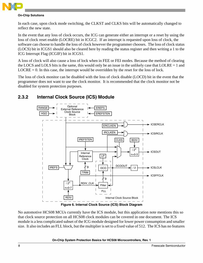
2.3.2 Internal Clock Source (ICS) Module
Figure 6. Internal Clock Source (ICS) Block Diagram
No automotive HCS08 MCUs currently have the ICS module, but this application note mentions this so that clock source protection on all HCS08 clock modules can be covered in one document. The ICS module is a less complicated subset of the ICG module designed for lower power consumption and smaller size. It also includes an FLL block, but the multiplier is set to a fixed value of 512. The ICS has no features
DCO
Filter
RDIV
TRIM
/ 2
9
External Reference
IREFS
Clock SourceBlock
CLKS
n=0-7
/ 2n
n=0-3
/ 2n
InternalReference
Clock
BDIV
9 ICSLCLK
ICSOUT
ICSIRCLK
EREFSRANGE
EREFSTENHGO
Optional
IREFSTEN
ICSERCLK
Internal Clock Source Block
LP
ICSFFCLK
ERCLKEN
IRCLKEN
DCOOUT
FLL
RDIV_CLK
On-Chip System Protection Basics for HCS08 Microcontrollers, Rev. 1
Freescale Semiconductor8

On-Chip Solutions
for monitoring either loss of clock or loss of lock. However, some HCS08 MCUs do provide a completely independent clock source for the COP watchdog timer that can reset the MCU if the CPU and bus clocks are corrupted. If loss of clock occurs, the software can no longer feed the COP watchdog and the MCU will reset. How quickly the reset occurs and recovers the system depends on the COP timeout period set by the software. The COP watchdog will be discussed in more detail later in this application note. In the event of loss of lock, the ICS will attempt to regain FLL lock on its own.
2.3.3 Multi-Purpose Clock Generator (MCG) Module
Figure 7. Multi-Purpose Clock Generator (MCG) Block Diagram
The MCG module includes the ICS as a sub-module with the added functionality of a phase-locked loop (PLL) controllable by either an external or internal reference clock. For clock system protection, it includes a clock monitor which detects loss of lock and loss of clock events.
DCO
Filter
RDIV
TRIM
External Oscillator
IREFS
(XOSC)
CLKS
n=0-7
/ 2n
n=0-3
/ 2n
InternalReference
Clock
BDIV
9
MCGLCLK
MCGOUT
MCGIRCLK
EREFSRANGE
EREFSTENHGO
IREFSTEN
MCGERCLK
LP
MCGFFCLK
DCOOUT
FLL
RDIV_CLK
PLL
VDIV
/(4,8,12,...,40)
VCOPhase
DetectorChargePump
InternalFilter
LockDetector
LOCK
ClockMonitor
OSCINIT
VCOOUT
Multi-purpose Clock Generator (MCG)
LP
ERCLKEN
IRCLKEN
CME
LOC
/ 2
PLLS
LOLS
On-Chip System Protection Basics for HCS08 Microcontrollers, Rev. 1
Freescale Semiconductor 9
On-Chip Solutions
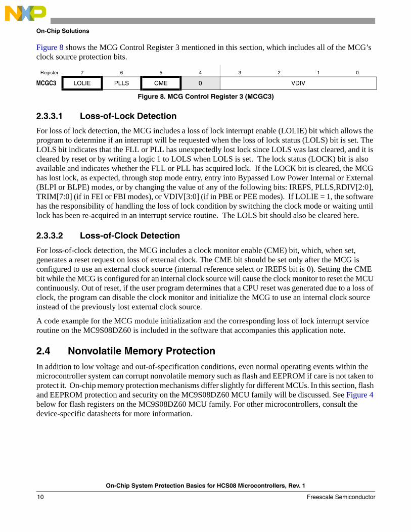
Figure 8 shows the MCG Control Register 3 mentioned in this section, which includes all of the MCG’s clock source protection bits.
Figure 8. MCG Control Register 3 (MCGC3)
2.3.3.1 Loss-of-Lock Detection
For loss of lock detection, the MCG includes a loss of lock interrupt enable (LOLIE) bit which allows the program to determine if an interrupt will be requested when the loss of lock status (LOLS) bit is set. The LOLS bit indicates that the FLL or PLL has unexpectedly lost lock since LOLS was last cleared, and it is cleared by reset or by writing a logic 1 to LOLS when LOLS is set. The lock status (LOCK) bit is also available and indicates whether the FLL or PLL has acquired lock. If the LOCK bit is cleared, the MCG has lost lock, as expected, through stop mode entry, entry into Bypassed Low Power Internal or External (BLPI or BLPE) modes, or by changing the value of any of the following bits: IREFS, PLLS,RDIV[2:0], TRIM[7:0] (if in FEI or FBI modes), or VDIV[3:0] (if in PBE or PEE modes). If LOLIE = 1, the software has the responsibility of handling the loss of lock condition by switching the clock mode or waiting until lock has been re-acquired in an interrupt service routine. The LOLS bit should also be cleared here.
2.3.3.2 Loss-of-Clock Detection
For loss-of-clock detection, the MCG includes a clock monitor enable (CME) bit, which, when set, generates a reset request on loss of external clock. The CME bit should be set only after the MCG is configured to use an external clock source (internal reference select or IREFS bit is 0). Setting the CME bit while the MCG is configured for an internal clock source will cause the clock monitor to reset the MCU continuously. Out of reset, if the user program determines that a CPU reset was generated due to a loss of clock, the program can disable the clock monitor and initialize the MCG to use an internal clock source instead of the previously lost external clock source.
A code example for the MCG module initialization and the corresponding loss of lock interrupt service routine on the MC9S08DZ60 is included in the software that accompanies this application note.
2.4 Nonvolatile Memory ProtectionIn addition to low voltage and out-of-specification conditions, even normal operating events within the microcontroller system can corrupt nonvolatile memory such as flash and EEPROM if care is not taken to protect it. On-chip memory protection mechanisms differ slightly for different MCUs. In this section, flash and EEPROM protection and security on the MC9S08DZ60 MCU family will be discussed. See Figure 4 below for flash registers on the MC9S08DZ60 MCU family. For other microcontrollers, consult the device-specific datasheets for more information.
Register 7 6 5 4 3 2 1 0
MCGC3 LOLIE PLLS CME 0 VDIV
On-Chip System Protection Basics for HCS08 Microcontrollers, Rev. 1
Freescale Semiconductor10

On-Chip Solutions
Table 4. Flash Registers on the MC9S08DZ60
2.4.1 Block Protection
Freescale microcontrollers include block-protection features for some or all nonvolatile memory to prevent unintended erasures or programming. On the MC9S08DZ60 MCU family, the flash and EEPROM protection register (FPROT) controls block protection. The EPS bits determine the protected region of EEPROM, and the FPS bits determine the protected region of flash. Refer to the device specific data sheet for detailed information on the memory blocks protected by these bits.
A user program cannot set or clear the FPROT register. Instead, after an exit from reset, FPROT is loaded with the contents of the NVPROT location, which is in the nonvolatile register block of the flash memory and cannot be altered by application software. The EPS and FPS bits can be set in the NVPROT location during programming to enable block protection. The only other way FPROT can be written is through background debug commands, which provide a way to erase and reprogram protected memory.
One use for block protection is to block-protect an area of flash memory for a bootloader program. This bootloader program can then erase the rest of the flash memory and reprogram it. The bootloader is protected even if MCU power is lost during an erase and reprogram operation. The block size of protected flash can be adjusted with the FPS bits to fit the size of the bootloader.
While any flash is block-protected, the reset and interrupt vectors will be protected. Vector redirection allows users to modify interrupt-vector information without unprotecting bootloader and reset vector space. Vector redirection is enabled by programming the FNORED bit in the NVOPT register to 0. For redirection, some portion of the flash memory must be block protected by programming the NVPROT register. All interrupt vectors except the reset vector are redirected. For more information, see the Vector Redirection chapter in the device-specific data sheet.
2.4.2 Security
In addition to flash block protection, Freescale microcontrollers include circuitry for security to prevent unauthorized access to the contents of flash, EEPROM (when included), and RAM memory. Direct-page registers, high-page registers, and the backrgound debug controller are unsecure resources and can be accessed whether security is engaged or not. Any attempts to access a secure memory location with a program executing from an unsecured memory space or through the background debug interface are blocked (writes are ignored and reads return all 0s).
Register
FCDIV
FOPT
FTSTMOD
FCNFG
FPROT
FSTAT
FCMD
7 6 5 4 3 2 1 0
DIVLD PRDIV8 DIV
KEYEN FNORED EPGMOD 0 0 0 SEC
0 MRDS 0 0 0 0 0
0 EPGSEL KEYACC 1 0 0 0 0
EPS FPS
FCBEF FCCF FPVIOL FACCERR 0 FBLANK 0 0
FCMD
On-Chip System Protection Basics for HCS08 Microcontrollers, Rev. 1
Freescale Semiconductor 11
On-Chip Solutions
Security is engaged or disengaged based on the state of two register bits (SEC[1:0]) in the FOPT register. Security is disengaged when SEC bits are set to 1:0. All other states, including the erased state (1:1), make the MCU secure. Because the user program cannot write directly to the FOPT register, the SEC bits can be programmed only to the nonvolatile NVOPT location, which can be performed simultaneously as the flash memory is programmed. During reset, the NVOPT register contents are copied from flash into the working FOPT register in high-page register space.
During development, whenever the flash is erased, it is good practice to program the SEC0 bit to immediately to 0 in NVOPT so SEC = 1:0. This allows the MCU to remain unsecured after a subsequent reset. The on-chip debug module cannot be enabled while the MCU is secure. The separate background debug controller can be used for background memory access commands, but the MCU cannot enter active background mode except by holding BKGD low at the rising edge of reset.
For more information on security and the process to disengage security, refer to the security section of the Memory Map and Register Definition chapter in the device specific data sheet.
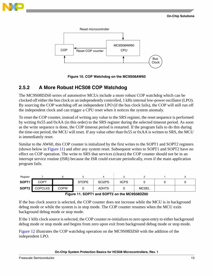
2.5 Computer-Operating Properly (COP) WatchdogAn internal COP watchdog is included on all HCS08 microcontrollers to reset the microcontroller when application software fails to execute as expected. A COP watchdog includes a timer that counts up to a certain period before timing out. Once the COP times out, it generates a system reset and the MCU returns to a known state. To prevent a COP reset, the application software must execute the proper clearing sequence before the COP timer times out. Because there are multiple COP watchdog implementations on different HCS08 microcontrollers, check the device-specific data sheet to determine the version used by a particular MCU.
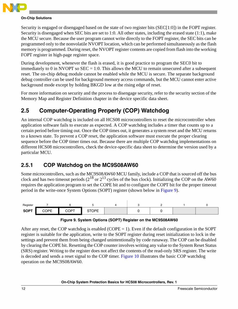
2.5.1 COP Watchdog on the MC9S08AW60
Some microcontrollers, such as the MC9S08AW60 MCU family, include a COP that is sourced off the bus clock and has two timeout periods (218 or 213 cycles of the bus clock). Initializing the COP on the AW60 requires the application program to set the COPE bit and to configure the COPT bit for the proper timeout period in the write-once System Options (SOPT) register (shown below in Figure 9).
Figure 9. System Options (SOPT) Register on the MC9S08AW60
After any reset, the COP watchdog is enabled (COPE = 1). Even if the default configuration in the SOPT register is suitable for the application, write to the SOPT register during reset initialization to lock in the settings and prevent them from being changed unintentionally by code runaway. The COP can be disabled by clearing the COPE bit. Resetting the COP counter involves writing any value to the System Reset Status (SRS) register. Writing to the register does not affect the contents of the read-only SRS register. The write is decoded and sends a reset signal to the COP timer. Figure 10 illustrates the basic COP watchdog operation on the MC9S08AW60.
Register 7 6 5 4 3 2 1 0
SOPT COPE COPT STOPE 0 0
On-Chip System Protection Basics for HCS08 Microcontrollers, Rev. 1
Freescale Semiconductor12
On-Chip Solutions
Figure 10. COP Watchdog on the MC9S08AW60
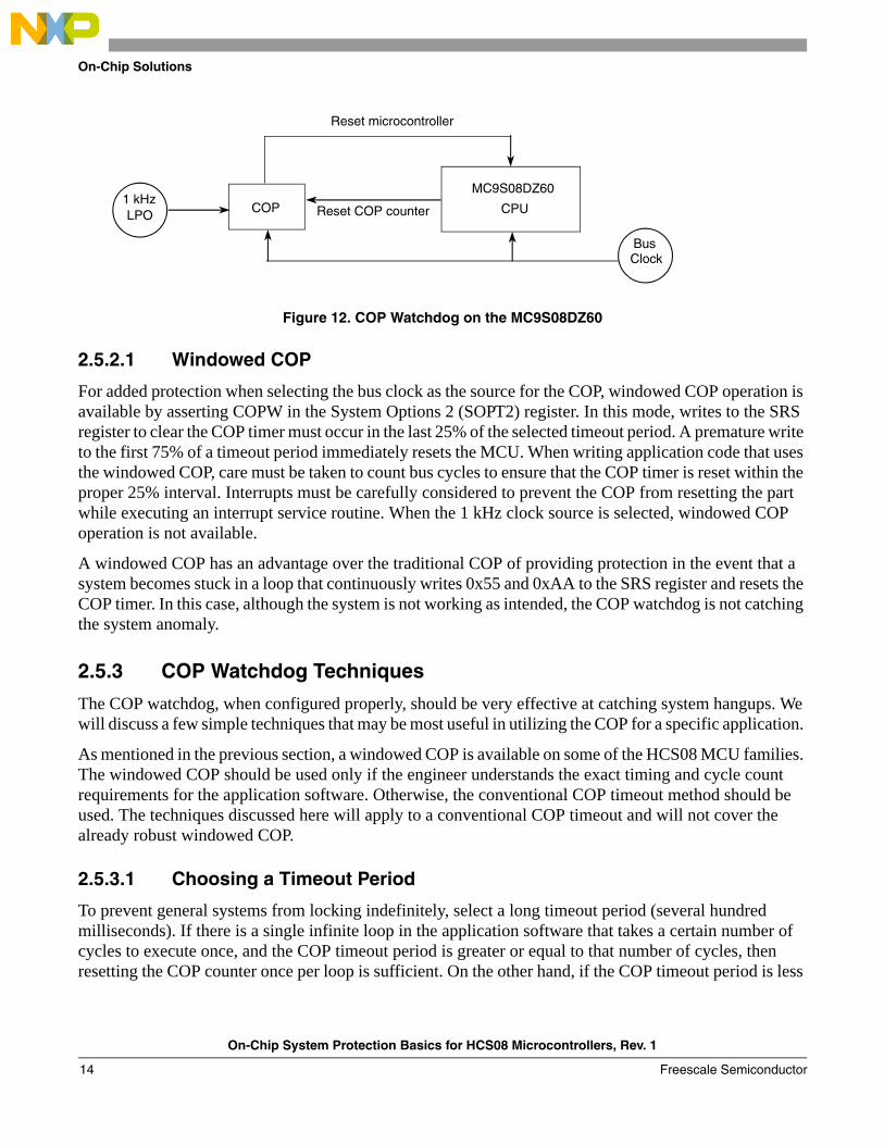
2.5.2 A More Robust HCS08 COP Watchdog
The MC9S08DZ60 series of automotive MCUs include a more robust COP watchdog which can be clocked off either the bus clock or an independently controlled, 1 kHz internal low-power oscillator (LPO). By sourcing the COP watchdog off an independent LPO (if the bus clock fails), the COP will still run off the independent clock and can trigger a CPU reset when it notices the system anomaly.
To reset the COP counter, instead of writing any value to the SRS register, the reset sequence is performed by writing 0x55 and 0xAA (in this order) to the SRS register during the selected timeout period. As soon as the write sequence is done, the COP timeout period is restarted. If the program fails to do this during the time-out period, the MCU will reset. If any value other than 0x55 or 0xAA is written to SRS, the MCU is immediately reset.
Similar to the AW60, this COP counter is initialized by the first writes to the SOPT1 and SOPT2 registers (shown below in Figure 11) and after any system reset. Subsequent writes to SOPT1 and SOPT2 have no effect on COP operation. The write to SRS that services (clears) the COP counter should not be in an interrupt service routine (ISR) because the ISR could execute periodically, even if the main application program fails.
Figure 11. SOPT1 and SOPT2 on the MC9S08DZ60
If the bus clock source is selected, the COP counter does not increase while the MCU is in background debug mode or while the system is in stop mode. The COP counter resumes when the MCU exits background debug mode or stop mode.
If the 1 kHz clock source is selected, the COP counter re-initializes to zero upon entry to either background debug mode or stop mode and begins from zero upon exit from background debug mode or stop mode.
Figure 12 illustrates the COP watchdog operation on the MC9S08DZ60 with the addition of the independent LPO.
Register 7 6 5 4 3 2 1 0
SOPT1 COPT STOPE SCI2PS IICPS 0 0 0
SOPT2 COPCLKS COPW 0 ADHTS 0 MCSEL
MC9S08AW60
CPUCOP
Reset microcontroller
Reset COP counter
BusClock
On-Chip System Protection Basics for HCS08 Microcontrollers, Rev. 1
Freescale Semiconductor 13
On-Chip Solutions
Figure 12. COP Watchdog on the MC9S08DZ60
2.5.2.1 Windowed COP
For added protection when selecting the bus clock as the source for the COP, windowed COP operation is available by asserting COPW in the System Options 2 (SOPT2) register. In this mode, writes to the SRS register to clear the COP timer must occur in the last 25% of the selected timeout period. A premature write to the first 75% of a timeout period immediately resets the MCU. When writing application code that uses the windowed COP, care must be taken to count bus cycles to ensure that the COP timer is reset within the proper 25% interval. Interrupts must be carefully considered to prevent the COP from resetting the part while executing an interrupt service routine. When the 1 kHz clock source is selected, windowed COP operation is not available.
A windowed COP has an advantage over the traditional COP of providing protection in the event that a system becomes stuck in a loop that continuously writes 0x55 and 0xAA to the SRS register and resets the COP timer. In this case, although the system is not working as intended, the COP watchdog is not catching the system anomaly.
2.5.3 COP Watchdog Techniques
The COP watchdog, when configured properly, should be very effective at catching system hangups. We will discuss a few simple techniques that may be most useful in utilizing the COP for a specific application.
As mentioned in the previous section, a windowed COP is available on some of the HCS08 MCU families. The windowed COP should be used only if the engineer understands the exact timing and cycle count requirements for the application software. Otherwise, the conventional COP timeout method should be used. The techniques discussed here will apply to a conventional COP timeout and will not cover the already robust windowed COP.
2.5.3.1 Choosing a Timeout Period
To prevent general systems from locking indefinitely, select a long timeout period (several hundred milliseconds). If there is a single infinite loop in the application software that takes a certain number of cycles to execute once, and the COP timeout period is greater or equal to that number of cycles, then resetting the COP counter once per loop is sufficient. On the other hand, if the COP timeout period is less
MC9S08DZ60
CPUCOP
Reset microcontroller
Reset COP counter
BusClock
1 kHzLPO
On-Chip System Protection Basics for HCS08 Microcontrollers, Rev. 1
Freescale Semiconductor14
Additional System Protection Techniques
than the amount of time it takes to execute the infinite loop once, it may be necessary to reset the COP between subroutines or significant events.
In a situation where the software must loop until a certain event occurs (for example, waiting for the part to reach a certain temperature or waiting for a certain data value to be received through a communication interface), and the wait time is longer than the COP timeout period, it may be necessary to reset the COP counter within that loop. Although the general recommendation is to keep the COP reset process within the main program loop, there will be application-dependent situations such as this when it may be preferrable to reset the COP counter within a loop or other procedure.
2.5.3.2 Resetting the COP Counter
Instead of periodically resetting the COP counter after loops or throughout code, it may be beneficial to include checks in strategic places before resetting the COP counter. For example, when running through a looping structure in code, to ensure that certain important events within the structure actually occur, the software can initialize a set of flag variables to ‘FALSE’ before entering the loop structure. Then, the software can set individual flags to ‘TRUE’ after each of the important events within the structure. At the end of the loop, only after all of the flags are ‘TRUE’ can the software reset the COP counter. Otherwise, clear all flags to ‘FALSE’ to log a failure and return to the loop beginning. If the events within the loop structure continuously fail to execute, the COP will eventually reset the CPU. It may also be useful to use the flags to indicate which event in the structure failed to execute properly and log this information before the MCU is reset.
2.5.3.3 COP Reset Recovery
After a COP reset, the COP bit in the system reset source (SRS) register will become set. It is up to the application developer to determine how a COP reset recovery should be handled. For a quick system recovery, the initialization process should be shorter than that of a normal power-on or pin reset. If an error was logged before the COP reset, the recovery routine can determine whether to continue to re-start the program or to take an action relevant to the error that occurred (for example, flash a LED, enter an error handling routine, etc.).
3 Additional System Protection TechniquesAlthough many system protection modules are available directly on the S08 microcontrollers, some user responsibility is involved in system protection as well. This section explains some additional techniques and methods that can be applied in an application to ensure robust system protection.
3.1 Filling Unused MemoryIn the event that code runaway occurs, the MCU could continue accessing memory until it reaches an illegal address where, finally, a system reset will occur. In the meantime, many undesired events could happen as a result of the code running where it should not. To protect from the potentially harmful effects of code runaway, it is generally good practice to fill unused memory with known values such as software interrupt (SWI) op-codes, illegal op-codes, or NOPs.
On-Chip System Protection Basics for HCS08 Microcontrollers, Rev. 1
Freescale Semiconductor 15
Additional System Protection Techniques
While debugging application code, the best practice is to fill unused memory with SWI (0x83 op-code value) instructions so that if code runaway occurs, an interrupt handler can inform the programmer if and where code runaway occurred.
In a finished application after the debugging process has ended, it is best to fill unused memory with illegal op-codes or NOPs to generate a near-immediate reset upon code runaway. Because S08 MCUs include an illegal op-code reset, if unused memory is filled with all illegal op-codes (0xAC or 0x8D op-code values), as soon as the MCU runs into an illegal op-code, the CPU will reset itself and set the ILOP bit in the SRS register to 1.
When filling the memory with NOPs, a good idea is to include SWI instructions periodically throughout the NOPs to cause the MCU to jump to an error handling interrupt routine. The SWI interrupt service routine can then generate a reset or error message indicating that code runaway or an illegal memory access has occurred. Another option is to include illegal op-code instructions at the end of the line of NOPs and SWIs. If the SWI has not already generated a reset, the MCU will reset once it has run through the NOP-filled memory and hit an illegal op-code.
3.1.1 Examples
This section includes three examples to illustrate different methods for filling unused memory in code.
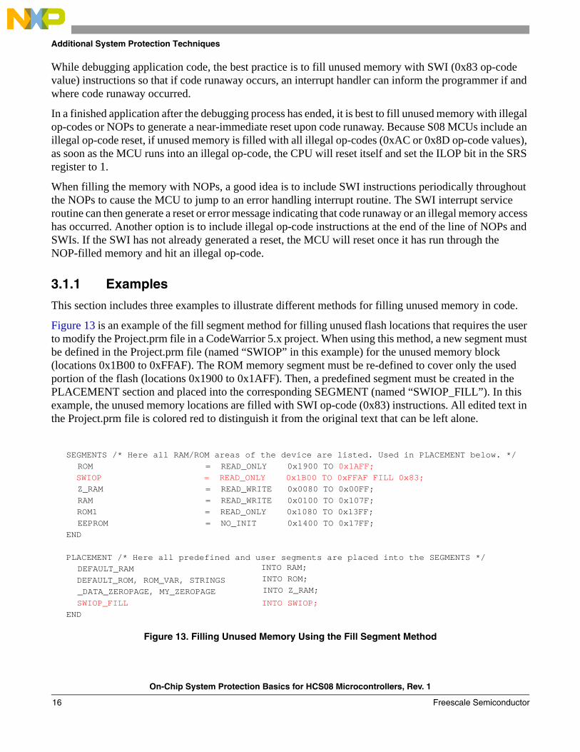
Figure 13 is an example of the fill segment method for filling unused flash locations that requires the user to modify the Project.prm file in a CodeWarrior 5.x project. When using this method, a new segment must be defined in the Project.prm file (named “SWIOP” in this example) for the unused memory block (locations 0x1B00 to 0xFFAF). The ROM memory segment must be re-defined to cover only the used portion of the flash (locations 0x1900 to 0x1AFF). Then, a predefined segment must be created in the PLACEMENT section and placed into the corresponding SEGMENT (named “SWIOP_FILL”). In this example, the unused memory locations are filled with SWI op-code (0x83) instructions. All edited text in the Project.prm file is colored red to distinguish it from the original text that can be left alone.
Figure 13. Filling Unused Memory Using the Fill Segment Method
SEGMENTS /* Here all RAM/ROM areas of the device are listed. Used in PLACEMENT below. */ ROM = READ_ONLY 0x1900 TO 0x1AFF;
SWIOP = READ_ONLY 0x1B00 TO 0xFFAF FILL 0x83; Z_RAM = READ_WRITE 0x0080 TO 0x00FF; RAM = READ_WRITE 0x0100 TO 0x107F; ROM1 = READ_ONLY 0x1080 TO 0x13FF; EEPROM = NO_INIT 0x1400 TO 0x17FF;END
PLACEMENT /* Here all predefined and user segments are placed into the SEGMENTS */ DEFAULT_RAM DEFAULT_ROM, ROM_VAR, STRINGS _DATA_ZEROPAGE, MY_ZEROPAGE SWIOP_FILL END
INTO RAM;INTO ROM;INTO Z_RAM;
INTO SWIOP;
On-Chip System Protection Basics for HCS08 Microcontrollers, Rev. 1
Freescale Semiconductor16
Additional System Protection Techniques
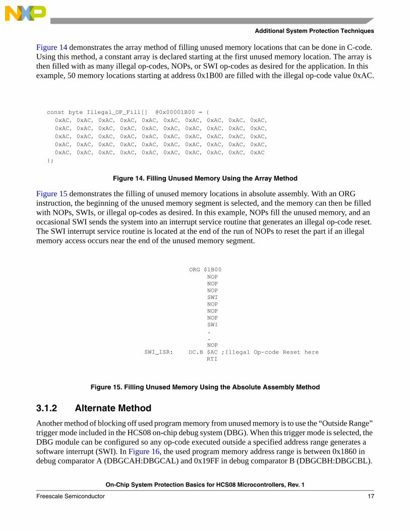
Figure 14 demonstrates the array method of filling unused memory locations that can be done in C-code. Using this method, a constant array is declared starting at the first unused memory location. The array is then filled with as many illegal op-codes, NOPs, or SWI op-codes as desired for the application. In this example, 50 memory locations starting at address 0x1B00 are filled with the illegal op-code value 0xAC.
Figure 14. Filling Unused Memory Using the Array Method
Figure 15 demonstrates the filling of unused memory locations in absolute assembly. With an ORG instruction, the beginning of the unused memory segment is selected, and the memory can then be filled with NOPs, SWIs, or illegal op-codes as desired. In this example, NOPs fill the unused memory, and an occasional SWI sends the system into an interrupt service routine that generates an illegal op-code reset. The SWI interrupt service routine is located at the end of the run of NOPs to reset the part if an illegal memory access occurs near the end of the unused memory segment.
Figure 15. Filling Unused Memory Using the Absolute Assembly Method
3.1.2 Alternate Method
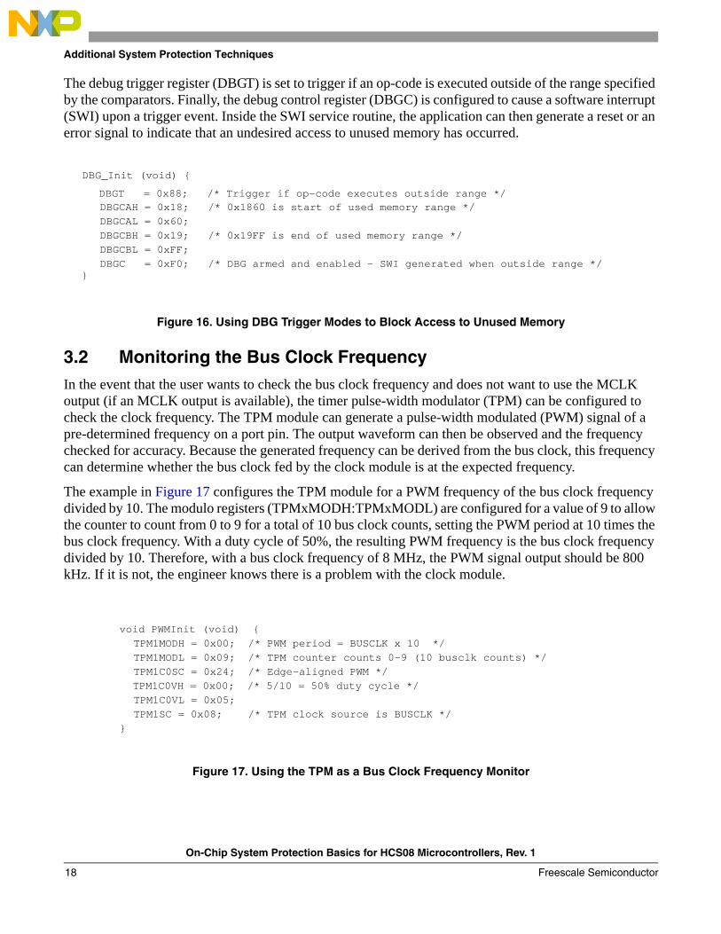
Another method of blocking off used program memory from unused memory is to use the “Outside Range” trigger mode included in the HCS08 on-chip debug system (DBG). When this trigger mode is selected, the DBG module can be configured so any op-code executed outside a specified address range generates a software interrupt (SWI). In Figure 16, the used program memory address range is between 0x1860 in debug comparator A (DBGCAH:DBGCAL) and 0x19FF in debug comparator B (DBGCBH:DBGCBL).
const byte Illegal_OP_Fill[] @0x00001B00 = { 0xAC, 0xAC, 0xAC, 0xAC, 0xAC, 0xAC, 0xAC, 0xAC, 0xAC, 0xAC, 0xAC, 0xAC, 0xAC, 0xAC, 0xAC, 0xAC, 0xAC, 0xAC, 0xAC, 0xAC, 0xAC, 0xAC, 0xAC, 0xAC, 0xAC, 0xAC, 0xAC, 0xAC, 0xAC, 0xAC, 0xAC, 0xAC, 0xAC, 0xAC, 0xAC, 0xAC, 0xAC, 0xAC, 0xAC, 0xAC, 0xAC, 0xAC, 0xAC, 0xAC, 0xAC, 0xAC, 0xAC, 0xAC, 0xAC, 0xAC};
ORG $1B00NOPNOPNOPSWINOPNOPNOPSWI..NOP
DC.B $AC ;Illegal Op-code Reset hereSWI_ISR:RTI
On-Chip System Protection Basics for HCS08 Microcontrollers, Rev. 1
Freescale Semiconductor 17
Additional System Protection Techniques
The debug trigger register (DBGT) is set to trigger if an op-code is executed outside of the range specified by the comparators. Finally, the debug control register (DBGC) is configured to cause a software interrupt (SWI) upon a trigger event. Inside the SWI service routine, the application can then generate a reset or an error signal to indicate that an undesired access to unused memory has occurred.
Figure 16. Using DBG Trigger Modes to Block Access to Unused Memory
3.2 Monitoring the Bus Clock FrequencyIn the event that the user wants to check the bus clock frequency and does not want to use the MCLK output (if an MCLK output is available), the timer pulse-width modulator (TPM) can be configured to check the clock frequency. The TPM module can generate a pulse-width modulated (PWM) signal of a pre-determined frequency on a port pin. The output waveform can then be observed and the frequency checked for accuracy. Because the generated frequency can be derived from the bus clock, this frequency can determine whether the bus clock fed by the clock module is at the expected frequency.
The example in Figure 17 configures the TPM module for a PWM frequency of the bus clock frequency divided by 10. The modulo registers (TPMxMODH:TPMxMODL) are configured for a value of 9 to allow the counter to count from 0 to 9 for a total of 10 bus clock counts, setting the PWM period at 10 times the bus clock frequency. With a duty cycle of 50%, the resulting PWM frequency is the bus clock frequency divided by 10. Therefore, with a bus clock frequency of 8 MHz, the PWM signal output should be 800 kHz. If it is not, the engineer knows there is a problem with the clock module.
Figure 17. Using the TPM as a Bus Clock Frequency Monitor
DBGCAH = 0x18; /* 0x1860 is start of used memory range */DBGCAL = 0x60;DBGCBH = 0x19; /* 0x19FF is end of used memory range */DBGCBL = 0xFF; DBGC = 0xF0; /* DBG armed and enabled - SWI generated when outside range */
DBGT = 0x88; /* Trigger if op-code executes outside range */
DBG_Init (void) {
}
void PWMInit (void) { TPM1MODH = 0x00; /* PWM period = BUSCLK x 10 */ TPM1MODL = 0x09; /* TPM counter counts 0-9 (10 busclk counts) */ TPM1C0SC = 0x24; /* Edge-aligned PWM */ TPM1C0VH = 0x00; /* 5/10 = 50% duty cycle */ TPM1C0VL = 0x05; TPM1SC = 0x08; /* TPM clock source is BUSCLK */}
On-Chip System Protection Basics for HCS08 Microcontrollers, Rev. 1
Freescale Semiconductor18
Additional System Protection Techniques
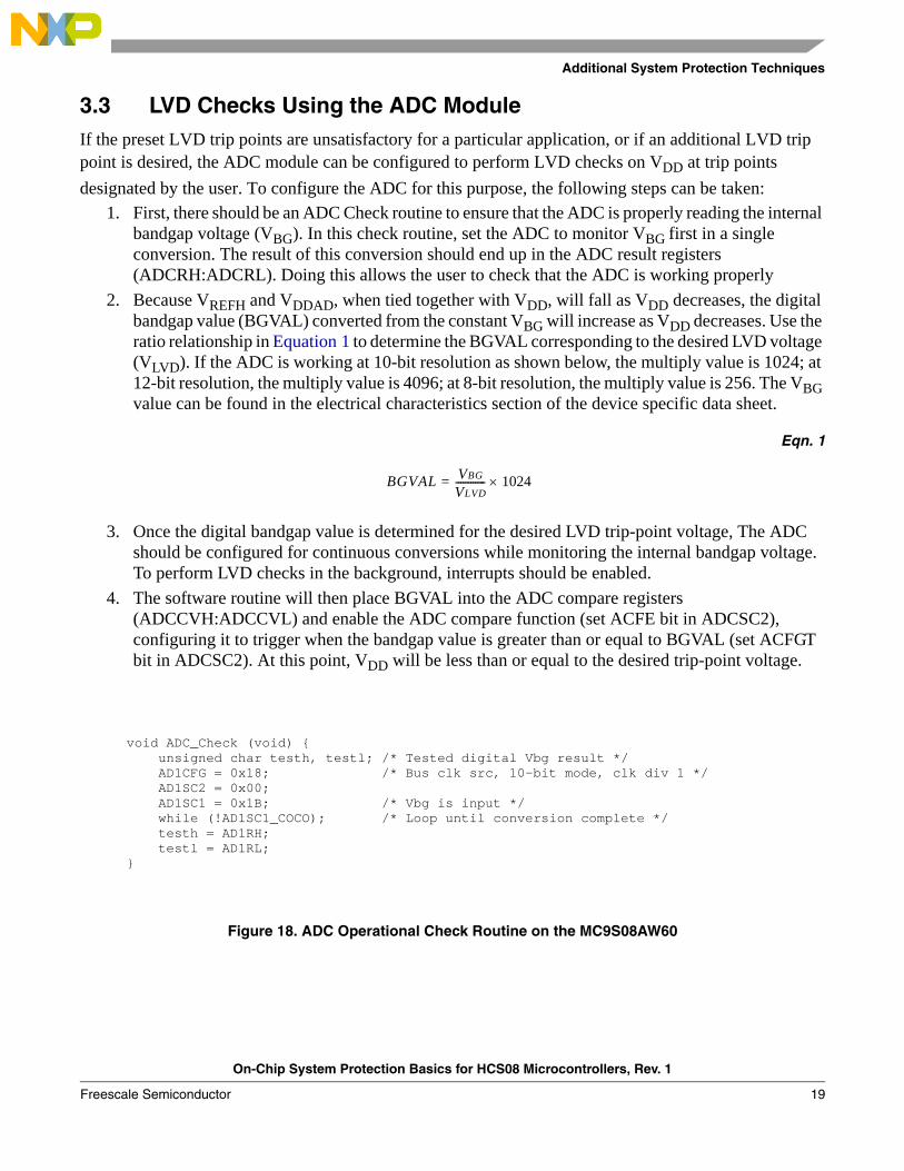
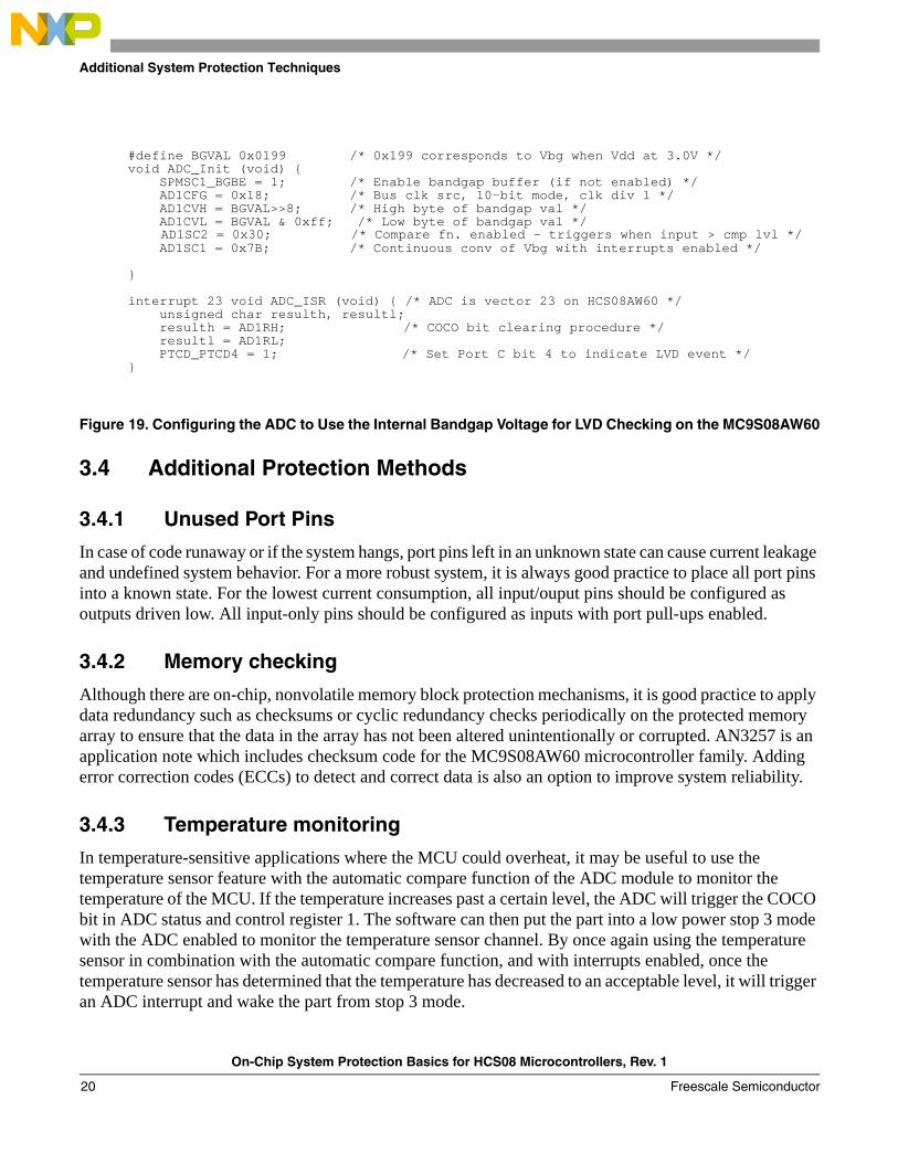
3.3 LVD Checks Using the ADC ModuleIf the preset LVD trip points are unsatisfactory for a particular application, or if an additional LVD trip point is desired, the ADC module can be configured to perform LVD checks on VDD at trip points designated by the user. To configure the ADC for this purpose, the following steps can be taken:
1. First, there should be an ADC Check routine to ensure that the ADC is properly reading the internal bandgap voltage (VBG). In this check routine, set the ADC to monitor VBG first in a single conversion. The result of this conversion should end up in the ADC result registers (ADCRH:ADCRL). Doing this allows the user to check that the ADC is working properly
2. Because VREFH and VDDAD, when tied together with VDD, will fall as VDD decreases, the digital bandgap value (BGVAL) converted from the constant VBG will increase as VDD decreases. Use the ratio relationship in Equation 1 to determine the BGVAL corresponding to the desired LVD voltage (VLVD). If the ADC is working at 10-bit resolution as shown below, the multiply value is 1024; at 12-bit resolution, the multiply value is 4096; at 8-bit resolution, the multiply value is 256. The VBG value can be found in the electrical characteristics section of the device specific data sheet.
Eqn. 1
3. Once the digital bandgap value is determined for the desired LVD trip-point voltage, The ADC should be configured for continuous conversions while monitoring the internal bandgap voltage. To perform LVD checks in the background, interrupts should be enabled.
4. The software routine will then place BGVAL into the ADC compare registers (ADCCVH:ADCCVL) and enable the ADC compare function (set ACFE bit in ADCSC2), configuring it to trigger when the bandgap value is greater than or equal to BGVAL (set ACFGT bit in ADCSC2). At this point, VDD will be less than or equal to the desired trip-point voltage.
Figure 18. ADC Operational Check Routine on the MC9S08AW60
BGVAL VBG
VLVD------------= 1024×
void ADC_Check (void) { unsigned char testh, testl; /* Tested digital Vbg result */ AD1CFG = 0x18; /* Bus clk src, 10-bit mode, clk div 1 */ AD1SC2 = 0x00; AD1SC1 = 0x1B; /* Vbg is input */ while (!AD1SC1_COCO); /* Loop until conversion complete */ testh = AD1RH; testl = AD1RL;}
On-Chip System Protection Basics for HCS08 Microcontrollers, Rev. 1
Freescale Semiconductor 19
Additional System Protection Techniques
Figure 19. Configuring the ADC to Use the Internal Bandgap Voltage for LVD Checking on the MC9S08AW60
3.4 Additional Protection Methods
3.4.1 Unused Port Pins
In case of code runaway or if the system hangs, port pins left in an unknown state can cause current leakage and undefined system behavior. For a more robust system, it is always good practice to place all port pins into a known state. For the lowest current consumption, all input/ouput pins should be configured as outputs driven low. All input-only pins should be configured as inputs with port pull-ups enabled.
3.4.2 Memory checking
Although there are on-chip, nonvolatile memory block protection mechanisms, it is good practice to apply data redundancy such as checksums or cyclic redundancy checks periodically on the protected memory array to ensure that the data in the array has not been altered unintentionally or corrupted. AN3257 is an application note which includes checksum code for the MC9S08AW60 microcontroller family. Adding error correction codes (ECCs) to detect and correct data is also an option to improve system reliability.
3.4.3 Temperature monitoring
In temperature-sensitive applications where the MCU could overheat, it may be useful to use the temperature sensor feature with the automatic compare function of the ADC module to monitor the temperature of the MCU. If the temperature increases past a certain level, the ADC will trigger the COCO bit in ADC status and control register 1. The software can then put the part into a low power stop 3 mode with the ADC enabled to monitor the temperature sensor channel. By once again using the temperature sensor in combination with the automatic compare function, and with interrupts enabled, once the temperature sensor has determined that the temperature has decreased to an acceptable level, it will trigger an ADC interrupt and wake the part from stop 3 mode.
#define BGVAL 0x0199 /* 0x199 corresponds to Vbg when Vdd at 3.0V */void ADC_Init (void) { SPMSC1_BGBE = 1; /* Enable bandgap buffer (if not enabled) */ AD1CFG = 0x18; /* Bus clk src, 10-bit mode, clk div 1 */ AD1CVH = BGVAL>>8; /* High byte of bandgap val */ AD1CVL = BGVAL & 0xff; /* Low byte of bandgap val */
AD1SC1 = 0x7B; /* Continuous conv of Vbg with interrupts enabled */ }
interrupt 23 void ADC_ISR (void) { /* ADC is vector 23 on HCS08AW60 */ unsigned char resulth, resultl; resulth = AD1RH; resultl = AD1RL; PTCD_PTCD4 = 1; }
/* COCO bit clearing procedure */
/* Set Port C bit 4 to indicate LVD event */
AD1SC2 = 0x30; /* Compare fn. enabled - triggers when input > cmp lvl */
On-Chip System Protection Basics for HCS08 Microcontrollers, Rev. 1
Freescale Semiconductor20
Application Example: Brownout Protection
4 Application Example: Brownout ProtectionIn the event of a brownout condition, memory locations can be unintentionally programmed and erased, code runaway can occur, and port pins can erratically change their states, potentially harming the overall system housing the microcontroller. To prevent this, the application software can use the on-chip solutions mentioned previously in this application note in combination to create a robust, protected system.
AN3305SW.zip includes a complete CodeWarrior 5.x project written in C for the MC9S08DZ60 with examples of many of the protection features mentioned in Section 2, “On-Chip Solutions.” In-line comments about how each feature works for brownout protection will be included with the code.
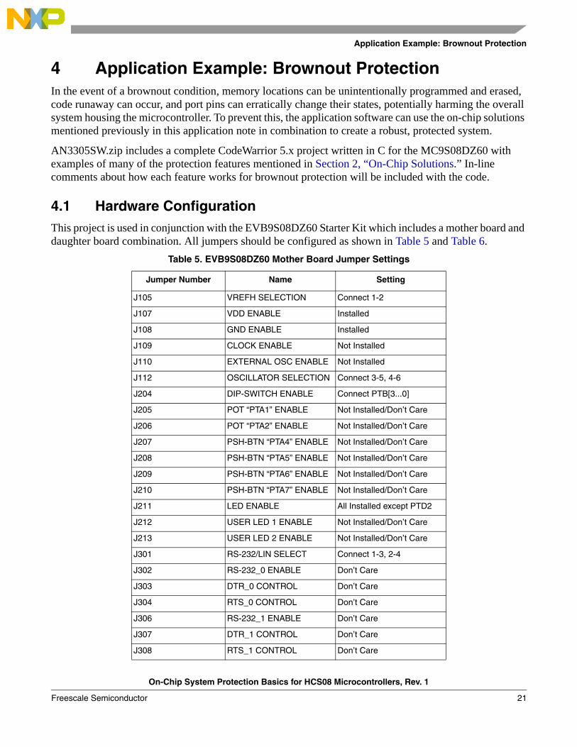
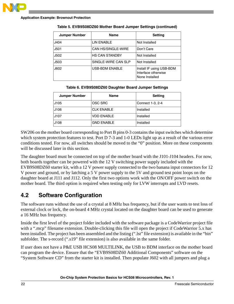
4.1 Hardware ConfigurationThis project is used in conjunction with the EVB9S08DZ60 Starter Kit which includes a mother board and daughter board combination. All jumpers should be configured as shown in Table 5 and Table 6.
Table 5. EVB9S08DZ60 Mother Board Jumper Settings
Jumper Number Name Setting
J105 VREFH SELECTION Connect 1-2
J107 VDD ENABLE Installed
J108 GND ENABLE Installed
J109 CLOCK ENABLE Not Installed
J110 EXTERNAL OSC ENABLE Not Installed
J112 OSCILLATOR SELECTION Connect 3-5, 4-6
J204 DIP-SWITCH ENABLE Connect PTB[3...0]
J205 POT “PTA1” ENABLE Not Installed/Don’t Care
J206 POT “PTA2” ENABLE Not Installed/Don’t Care
J207 PSH-BTN “PTA4” ENABLE Not Installed/Don’t Care
J208 PSH-BTN “PTA5” ENABLE Not Installed/Don’t Care
J209 PSH-BTN “PTA6” ENABLE Not Installed/Don’t Care
J210 PSH-BTN “PTA7” ENABLE Not Installed/Don’t Care
J211 LED ENABLE All Installed except PTD2
J212 USER LED 1 ENABLE Not Installed/Don’t Care
J213 USER LED 2 ENABLE Not Installed/Don’t Care
J301 RS-232/LIN SELECT Connect 1-3, 2-4
J302 RS-232_0 ENABLE Don’t Care
J303 DTR_0 CONTROL Don’t Care
J304 RTS_0 CONTROL Don’t Care
J306 RS-232_1 ENABLE Don’t Care
J307 DTR_1 CONTROL Don’t Care
J308 RTS_1 CONTROL Don’t Care
On-Chip System Protection Basics for HCS08 Microcontrollers, Rev. 1
Freescale Semiconductor 21
Application Example: Brownout Protection
SW206 on the mother board corresponding to Port B pins 0-3 contains the input switches which determine which system protection features to test. Port D 7-3 and 1-0 LEDs light up as a result of the various error conditions tested. For now, all switches should be moved to the “0” position. More on these components will be discussed later in this section.
The daughter board must be connected on top of the mother board with the J101-J104 headers. For now, both boards together can be powered with the 12 V switching power supply included with the EVB9S08DZ60 starter kit, with a 12 V power supply connected to the two banana input connectors for 12 V power and ground, or by latching a 5 V power supply to the 5V and ground test point loops on the daughter board at J111 and J112. Only the first two options work with the ON/OFF power switch on the mother board. The third option is required when testing only for LVW interrupts and LVD resets.
4.2 Software ConfigurationThe software runs without the use of a crystal at 8 MHz bus frequency, but if the user wants to test loss of external clock or lock, the on-board 4 MHz crystal located on the daughter board can be used to generate a 16 MHz bus frequency.
Inside the first level of the project folder included with the software package is a CodeWarrior project file with a “.mcp” filename extension. Double-clicking this file will open the project if CodeWarrior 5.x has been installed. The project has been assembled and the listing (“.lst” file extension) is available in the “bin” subfolder. The s-record (“.s19” file extension) is also available in the same folder.
If user does not have a P&E USB HCS08 MULTILINK, the USB to BDM interface on the mother board can program the device. Ensure that the “EVB9S08DZ60 Additional Components” software on the “System Software CD” from the starter kit is installed. Then populate J602 with all jumpers and plug a
J404 LIN ENABLE Not Installed
J501 CAN HS/SINGLE-WIRE Don’t Care
J502 HS CAN STANDBY Not Installed
J503 SINGLE-WIRE CAN SLP Not Installed
J602 USB-BDM ENABLE Install IF using USB-BDM Interface otherwise None Installed
Table 6. EVB9S08DZ60 Daughter Board Jumper Settings
Jumper Number Name Setting
J105 OSC SRC Connect 1-3, 2-4
J106 CLK ENABLE Installed
J107 VDD ENABLE Installed
J108 GND ENABLE Installed
Table 5. EVB9S08DZ60 Mother Board Jumper Settings (continued)
Jumper Number Name Setting
On-Chip System Protection Basics for HCS08 Microcontrollers, Rev. 1
Freescale Semiconductor22
Application Example: Brownout Protection
USB cable between the PC and the USB connector on the motherboard. Allow the PC to install the required components automatically after it recognizes the USB device.
Finally, to run the project, select “SofTec HCS08” (“P&E Multilink/Cyclone Pro” if using a P&E USB HCS08 MULTILINK) from the pull-down menu to the left of the CodeWarrior IDE window and click on the green debug arrow. By putting an oscilloscope probe (if available) on PTD2/TPM1Ch0, a waveform running at a frequency of fBUS/10 can be observed, which means the software is running. Close the debugger window to avoid MCU reset conflict with the USB to BDM interface.
1. To test the COP reset, switch PTB3 (switch 5) to the “1” position and reset the part (with the RESET button on the mother board). The software will attempt to reset the COP counter in an inappropriate time window, resulting in a continuous CPU reset as long as the switch is in the “1” position. Then switch PTB3 (switch 5) to the “0” position and notice that PTD0 is now lit, indicating a COP reset has occurred.
2. To test the ILOP reset, switch PTB1 (switch 7) to the “1” position and reset the part (with the RESET button on the mother board). The software will then jump to a location in flash which is filled with the illegal op-code 0xAC. This will cause the MCU to continuously reset as long as the switch is in the “1” position and the software continues to jump to the illegal op-code location. Then switch PTB1 (switch 7) to the “0” position and notice that PTD1 is now lit, indicating an ILOP reset has occurred.
3. To test an MCG loss of clock reset, switch PTB2 (switch 6) to the “1” position and reset the part (with the RESET button on the mother board). Disconnect the jumper on J105 (on the daughter board) between pins 1 and 3. This disconnects the crystal connection to EXTAL, resulting in a loss of clock. Notice that PTD4 immediately lights up.
4. To test the flash security feature, return the CodeWarrior IDE window and uncomment the following line located at the top of the “main.c” file by removing the “//” in front of the code: // const byte NVOPT_INIT @0x0000FFBF = 0x00; /* UNCOMMENT to enable security */
Then run the debugger by pushing the green arrow and notice that now none of the windows in the debugger have any content except the Memory window. Inside the memory window, all of the flash memory appears as “00” because it is secure. Re-commenting the line mentioned above by inserting “//” at the beginning of the line and running the debugger again will then make the source code and flash memory visible to the user.
5. To test the LVD reset and LVW interrupt, the user must connect an adjustable power supply set at 5 V to the 5 V and ground test point loops (J112 and J111 respectively) on the daughter board. By adjusting the power supply level between 4 and 5 V, the LVW interrupt and LVD reset can be tested. Be sure to close the debugger window again to prevent of USB-BDM connection loss.— To test for an LVW event, switch PTB0 (switch 8) to the “1” position and reset the part (with
the RESET button on the mother board). This turns off the COP for this demo because changing the power supply manually will continuously put the software into the LVW interrupt service routine as the voltage level slowly decreases, causing the COP timer to time out and reset the MCU. Slowly decrease the power supply to below 4.3 V. Once the LVW trip point has been reached, the PTD6 LED will turn on. Raise the power supply voltage above 4.7 V, and the LED will turn off, indicating that the system is out of the LVW danger zone.
On-Chip System Protection Basics for HCS08 Microcontrollers, Rev. 1
Freescale Semiconductor 23
Conclusion
— To test for an LVD reset, slowly decrease the power supply to below 4.0 V and then bring the power supply back up to 5.0 V again. Notice that now the PTD5 LED is on, indicating that an LVD reset has occurred.
6. An ILAD reset will turn on the PTD3 LED, and an MCG external clock loss of lock event will turn on the PTD7 LED, but these two system failures are not explicitly tested in the included software.
5 ConclusionSystem protection is essential in sensitive automotive applications. The HCS08 family of microcontrollers includes multiple on-chip solutions to increase the robustness of microcontroller systems, making them less susceptible to corruption by noise, software error, and other external or internal influences.
Below is a summary of the on-chip solutions discussed in this application note:• Low-Voltage Detect (LVD) System• Illegal Op-code and Illegal Address Resets• Clock Source System Protection• Flash Protection and Security• Computer Operating Properly (COP) Watchdog
By ensuring that all these solutions are configured properly in an application, the user can reduce the negative effects of external and internal anomalies to a microcontroller system.
6 ReferencesChristopher Leddy, “Avoid Corruption in Nonvolatile Memory,” Embedded Systems Programming (www.embedded.com), September 2003.
Niall Murphy and Michael Barr, “Watchdog Timers,” Embedded Systems Programming (www.embedded.com), October 2001.
Greg Racino, “Resetting Microcontrollers During Power Transitions,” Freescale Application Note AN1744/D, www.freescale.com.
Ross Mitchell, “Resetting MCUs,” Freescale Engineering Bulletin EB413, www.freescale.com.
John Suchyta, “Improving the Transient Immunity Performance of Microcontroller-Based Applications,” Freescale Application Note AN2764, www.freescale.com.
Dugald Campbell, “Meeting IEC 60730 Class B Compliance with the MC9S08AW60,” Freescale Application Note AN3257, www.freescale.com.
On-Chip System Protection Basics for HCS08 Microcontrollers, Rev. 1
Freescale Semiconductor24

THIS PAGE IS INTENTIONALLY BLANK
On-Chip System Protection Basics for HCS08 Microcontrollers, Rev. 1
Freescale Semiconductor 25
Document Number: AN3305Rev. 102/2007
How to Reach Us:
Home Page:www.freescale.com
E-mail:[email protected]
USA/Europe or Locations Not Listed:Freescale SemiconductorTechnical Information Center, CH3701300 N. Alma School RoadChandler, Arizona 85224+1-800-521-6274 or [email protected]
Europe, Middle East, and Africa:Freescale Halbleiter Deutschland GmbHTechnical Information CenterSchatzbogen 781829 Muenchen, Germany+44 1296 380 456 (English)+46 8 52200080 (English)+49 89 92103 559 (German)+33 1 69 35 48 48 (French)[email protected]
Japan:Freescale Semiconductor Japan Ltd.HeadquartersARCO Tower 15F1-8-1, Shimo-Meguro, Meguro-ku,Tokyo 153-0064Japan0120 191014 or +81 3 5437 [email protected]
Asia/Pacific:Freescale Semiconductor Hong Kong Ltd.Technical Information Center2 Dai King StreetTai Po Industrial EstateTai Po, N.T., Hong Kong+800 2666 [email protected]
For Literature Requests Only:Freescale Semiconductor Literature Distribution CenterP.O. Box 5405Denver, Colorado 802171-800-441-2447 or 303-675-2140Fax: [email protected]
Information in this document is provided solely to enable system and software implementers to use Freescale Semiconductor products. There are no express or implied copyright licenses granted hereunder to design or fabricate any integrated circuits or integrated circuits based on the information in this document.
Freescale Semiconductor reserves the right to make changes without further notice to any products herein. Freescale Semiconductor makes no warranty, representation or guarantee regarding the suitability of its products for any particular purpose, nor does Freescale Semiconductor assume any liability arising out of the application or use of any product or circuit, and specifically disclaims any and all liability, including without limitation consequential or incidental damages. “Typical” parameters that may be provided in Freescale Semiconductor data sheets and/or specifications can and do vary in different applications and actual performance may vary over time. All operating parameters, including “Typicals”, must be validated for each customer application by customer’s technical experts. Freescale Semiconductor does not convey any license under its patent rights nor the rights of others. Freescale Semiconductor products are not designed, intended, or authorized for use as components in systems intended for surgical implant into the body, or other applications intended to support or sustain life, or for any other application in which the failure of the Freescale Semiconductor product could create a situation where personal injury or death may occur. Should Buyer purchase or use Freescale Semiconductor products for any such unintended or unauthorized application, Buyer shall indemnify and hold Freescale Semiconductor and its officers, employees, subsidiaries, affiliates, and distributors harmless against all claims, costs, damages, and expenses, and reasonable attorney fees arising out of, directly or indirectly, any claim of personal injury or death associated with such unintended or unauthorized use, even if such claim alleges that Freescale Semiconductor was negligent regarding the design or manufacture of the part.
Freescale™ and the Freescale logo are trademarks of Freescale Semiconductor, Inc. All other product or service names are the property of their respective owners.
© Freescale Semiconductor, Inc. 2006. All rights reserved.
RoHS-compliant and/or Pb-free versions of Freescale products have the functionality and electrical characteristics as their non-RoHS-compliant and/or non-Pb-free counterparts. For further information, see http://www.freescale.com or contact your Freescale sales representative.
For information on Freescale’s Environmental Products program, go to http://www.freescale.com/epp.