Embed Size (px)
Citation preview
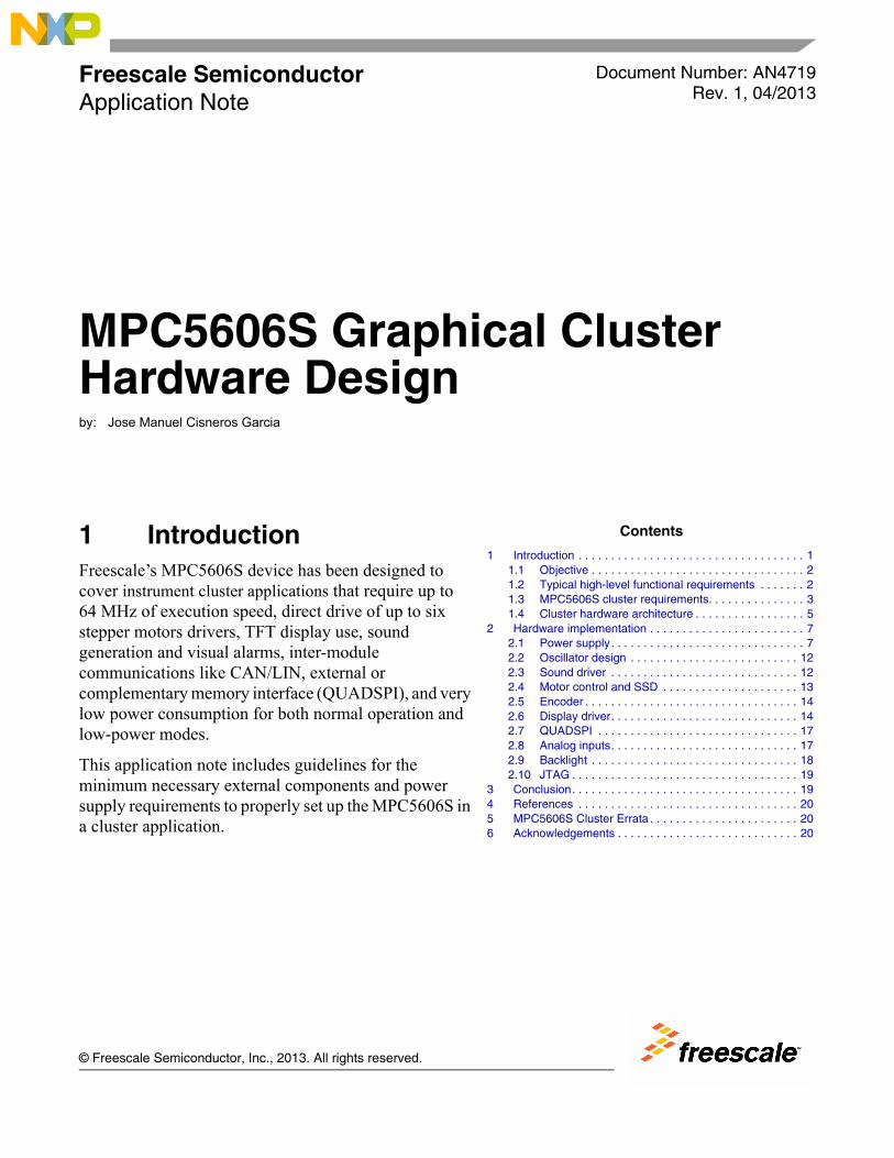
Freescale SemiconductorApplication Note
Document Number: AN4719Rev. 1, 04/2013
Contents
Introduction . . . . . . . . . . . . . . . . . . . . . . . . . . . . . . . . . . . 11.1 Objective . . . . . . . . . . . . . . . . . . . . . . . . . . . . . . . . . 21.2 Typical high-level functional requirements . . . . . . . 21.3 MPC5606S cluster requirements. . . . . . . . . . . . . . . 31.4 Cluster hardware architecture . . . . . . . . . . . . . . . . . 5Hardware implementation . . . . . . . . . . . . . . . . . . . . . . . . 7
2.1 Power supply . . . . . . . . . . . . . . . . . . . . . . . . . . . . . . 72.2 Oscillator design . . . . . . . . . . . . . . . . . . . . . . . . . . 122.3 Sound driver . . . . . . . . . . . . . . . . . . . . . . . . . . . . . 122.4 Motor control and SSD . . . . . . . . . . . . . . . . . . . . . 132.5 Encoder . . . . . . . . . . . . . . . . . . . . . . . . . . . . . . . . . 142.6 Display driver. . . . . . . . . . . . . . . . . . . . . . . . . . . . . 142.7 QUADSPI . . . . . . . . . . . . . . . . . . . . . . . . . . . . . . . 172.8 Analog inputs. . . . . . . . . . . . . . . . . . . . . . . . . . . . . 172.9 Backlight . . . . . . . . . . . . . . . . . . . . . . . . . . . . . . . . 182.10 JTAG . . . . . . . . . . . . . . . . . . . . . . . . . . . . . . . . . . . 19Conclusion. . . . . . . . . . . . . . . . . . . . . . . . . . . . . . . . . . . 19References . . . . . . . . . . . . . . . . . . . . . . . . . . . . . . . . . . 20MPC5606S Cluster Errata . . . . . . . . . . . . . . . . . . . . . . . 20Acknowledgements . . . . . . . . . . . . . . . . . . . . . . . . . . . . 20
MPC5606S Graphical Cluster Hardware Designby: Jose Manuel Cisneros Garcia
1 Introduction Freescale’s MPC5606S device has been designed to cover instrument cluster applications that require up to 64 MHz of execution speed, direct drive of up to six stepper motors drivers, TFT display use, sound generation and visual alarms, inter-module communications like CAN/LIN, external or complementary memory interface (QUADSPI), and very low power consumption for both normal operation and low-power modes.
This application note includes guidelines for the minimum necessary external components and power supply requirements to properly set up the MPC5606S in a cluster application.
1
2
3456
© Freescale Semiconductor, Inc., 2013. All rights reserved.

Introduction
NOTEThe schematics in this document are provided for reference purposes only. As such, Freescale does not make any warranty, implied or otherwise, as to the suitability of circuit design or component selection (type or value) used in these schematics for hardware design using the Freescale MPC5606S family of microprocessors. If you use any part of these schematics as a basis for hardware design, do so at their own risk; Freescale does not assume any liability for such a hardware design.
1.1 ObjectiveThis document aims to serve as a general guide for starting a design based on the MPC5606S. Starting from a set of requirements listed in Table 2, the final implementation is an automotive cluster module comprised of both hardware and software components. The following figure shows a picture of the MPC5606S cluster after it is complete.
Figure 1. MPC5606 instrument cluster
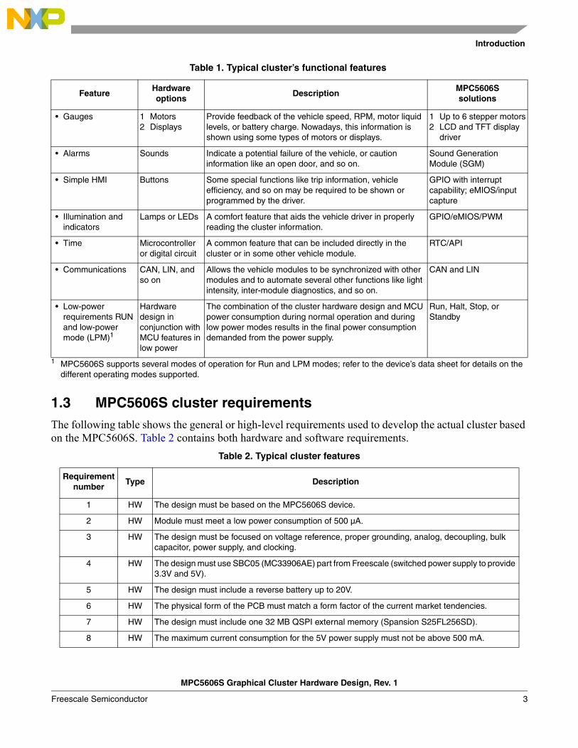
1.2 Typical high-level functional requirementsInstrument clusters are designed to provide to a driver the information required for a safe and comfortable drive. They indicate vehicle status and direction, indicate gear status, provide feedback on commanded functions (such as left and right turns), and sound alarms, just to name some of the types of information that clusters provide. To cover all these requirements, some vehicle manufacturers design their clusters based on some or all of the features included in Table 1. Notice that the features listed in this table are not the only ones and they have grown as vehicles and technology have evolved. The number of features that a cluster may include is limited by the manufacturer’s design and the market needs and for which the vehicle is designed.
MPC5606S Graphical Cluster Hardware Design, Rev. 1
Freescale Semiconductor2
Introduction
1.3 MPC5606S cluster requirementsThe following table shows the general or high-level requirements used to develop the actual cluster based on the MPC5606S. Table 2 contains both hardware and software requirements.
Table 1. Typical cluster’s functional features
FeatureHardwareoptions
DescriptionMPC5606Ssolutions
• Gauges 1 Motors2 Displays
Provide feedback of the vehicle speed, RPM, motor liquid levels, or battery charge. Nowadays, this information is shown using some types of motors or displays.
1 Up to 6 stepper motors2 LCD and TFT display
driver
• Alarms Sounds Indicate a potential failure of the vehicle, or caution information like an open door, and so on.
Sound Generation Module (SGM)
• Simple HMI Buttons Some special functions like trip information, vehicle efficiency, and so on may be required to be shown or programmed by the driver.
GPIO with interrupt capability; eMIOS/input capture
• Illumination and indicators
Lamps or LEDs A comfort feature that aids the vehicle driver in properly reading the cluster information.
GPIO/eMIOS/PWM
• Time Microcontroller or digital circuit
A common feature that can be included directly in the cluster or in some other vehicle module.
RTC/API
• Communications CAN, LIN, and so on
Allows the vehicle modules to be synchronized with other modules and to automate several other functions like light intensity, inter-module diagnostics, and so on.
CAN and LIN
• Low-power requirements RUN and low-power mode (LPM)1
1 MPC5606S supports several modes of operation for Run and LPM modes; refer to the device’s data sheet for details on the different operating modes supported.
Hardware design in conjunction with MCU features in low power
The combination of the cluster hardware design and MCU power consumption during normal operation and during low power modes results in the final power consumption demanded from the power supply.
Run, Halt, Stop, or Standby
Table 2. Typical cluster features
Requirement number
Type Description
1 HW The design must be based on the MPC5606S device.
2 HW Module must meet a low power consumption of 500 µA.
3 HW The design must be focused on voltage reference, proper grounding, analog, decoupling, bulk capacitor, power supply, and clocking.
4 HW The design must use SBC05 (MC33906AE) part from Freescale (switched power supply to provide 3.3V and 5V).
5 HW The design must include a reverse battery up to 20V.
6 HW The physical form of the PCB must match a form factor of the current market tendencies.
7 HW The design must include one 32 MB QSPI external memory (Spansion S25FL256SD).
8 HW The maximum current consumption for the 5V power supply must not be above 500 mA.
MPC5606S Graphical Cluster Hardware Design, Rev. 1
Freescale Semiconductor 3
Introduction
NOTEThis cluster implementation should not be used as a final solution but as a hardware guide to start developing a final cluster product.
In addition to the hardware and software design elements, the cluster application also requires a mechanical design that includes:
• A faceplate that shows the RPM, Temperature, Gas, and Odometer scales as well as the tell-tale icons. The faceplate is formed with two pieces: an acrylic or transparent plastic and a sticker or overlay that includes all the icons and scales.
• A plastic case or housing that goes in front of all the design, giving the appearance of a complete cluster. The plastic case was designed using a 3D modeling software (CAD). The advantage in using this type of software is that it allows you to export all the dimensions and vectors required to match the two pieces of the project—the electronic board and the plastic case—with excellent results.
9 HW The design must use a special purpose connector for all the external signals and power to emulate a real cluster.
10 HW The design must include one 4.2-inch TFT display (480 × 272 18-bit RGB) with integrated backlighting (Sharp LQ042T5DZ01).
11 HW The cluster must have four mechanic gauges: two big pointers (Speed and RPM) and two small pointers (Fuel and Temp).
12 HW The design must be enabled with a JTAG debugger connector.
13 HW The design must take into account EMC/ESD considerations, such as analog decoupling, bulk capacitors, and signal filtering
14 HW Low-Power mode should consume less than 500 µA.
15 Include 12 tell-tale icons driven from BATT with FETs (BSS138), with the following functions:
1 OVERTEMP2 CHECK ENGINE3 BREAK4 SEAT BELT5 LOW BATTERY6 LOW FUEL
7 LOW OIL8 ABS9 HI BEAM10 TURN LEFT11 TURN RIGHT12 FOG
16 HW Include amplification circuitry and a speaker to be used with the Sound Generation Module (SGM) included in the MPC5606S.
17 HW Enable hardware for CAN communications.
18 HW Enable hardware for LIN communications.
19 SW The SGM should emulate the hazard and the left/right turn relays emulation (mechanical relay sound).
20 SW Stepper motors must have stall detection for return to zero calibration at module startup and automatic position reset when turning the cluster on.
21 SW Implement graphics to be shown on the TFT display.
Table 2. Typical cluster features (continued)
Requirement number
Type Description
MPC5606S Graphical Cluster Hardware Design, Rev. 1
Freescale Semiconductor4
Introduction
Figure 2 shows an example of how a cluster prototype looks on the software design tool.
Figure 2. 3D Mechanical design example
Once the mechanical design is finished, it is printed using a 3D printer, then the plastic piece is ready to be assembled with the electronic board. This type of implementation provides a great highlight to the final prototype.
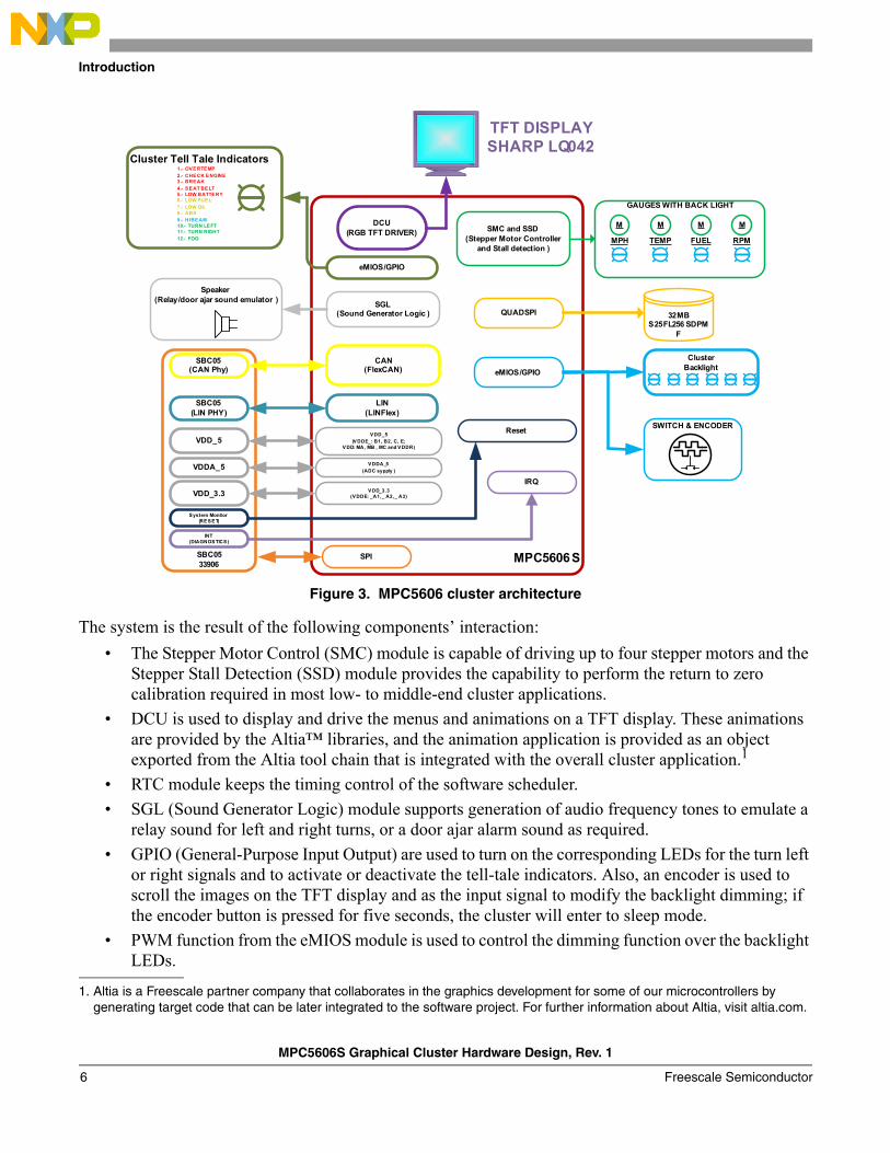
1.4 Cluster hardware architectureFigure 3 shows the MPC5606S modules to be used to cover the cluster reference design for this particular application note. Notice that this application does not use all the MPC5606S modules. For the additional features that this device supports, please refer to MPC5606SRM, MPC5606S Microcontroller Reference Manual, at freescale.com.
MPC5606S Graphical Cluster Hardware Design, Rev. 1
Freescale Semiconductor 5
Introduction
Figure 3. MPC5606 cluster architecture
The system is the result of the following components’ interaction:
• The Stepper Motor Control (SMC) module is capable of driving up to four stepper motors and the Stepper Stall Detection (SSD) module provides the capability to perform the return to zero calibration required in most low- to middle-end cluster applications.
• DCU is used to display and drive the menus and animations on a TFT display. These animations are provided by the Altia™ libraries, and the animation application is provided as an object exported from the Altia tool chain that is integrated with the overall cluster application.1
• RTC module keeps the timing control of the software scheduler.
• SGL (Sound Generator Logic) module supports generation of audio frequency tones to emulate a relay sound for left and right turns, or a door ajar alarm sound as required.
• GPIO (General-Purpose Input Output) are used to turn on the corresponding LEDs for the turn left or right signals and to activate or deactivate the tell-tale indicators. Also, an encoder is used to scroll the images on the TFT display and as the input signal to modify the backlight dimming; if the encoder button is pressed for five seconds, the cluster will enter to sleep mode.
• PWM function from the eMIOS module is used to control the dimming function over the backlight LEDs.
1. Altia is a Freescale partner company that collaborates in the graphics development for some of our microcontrollers by generating target code that can be later integrated to the software project. For further information about Altia, visit altia.com.
SBC0533906
MPC5606S
M
RPM
M
FUEL
M
TEMP
M
MPH
GAUGES WITH BACK LIGHT
SMC and SSD(Stepper Motor Controller
and Stall detection )
eMIOS/GPIO
SGL(Sound Generator Logic )
CAN (FlexCAN)
LIN(LINFlex)
QUADSPI
ClusterBacklight
Speaker(Relay/door ajar sound emulator )
SBC05 (CAN Phy)
eMIOS/GPIO
Cluster Tell Tale Indicators1.- OVERTEMP
2.- CHECK ENGINE3.- BREAK
4.- SEAT BELT5.- LOW BATTERY6.- LOW FUEL
7.- LOW OIL8.- ABS9.- HI BEAM10.- TURN LEFT11.- TURN RIGHT12.- FOG
DCU(RGB TFT DRIVER)
32MBS25FL256 SDPM
F
TFT DISPLAYSHARP LQ042
VDD_5
VDD_3.3
VDD_5(VDDE_: B1, B2, C, E;
V DD: MA, MB , MC and VDDR)
VDD_3.3(VDDE: _A1, _ A2, _ A3)
VDDA_5 VDDA_5
(ADC sypply )
SBC05(LIN PHY)
Reset
IRQ
INT (DIAGNOSTICS)
System Monitor(RESET)
SPI
SWITCH & ENCODER
MPC5606S Graphical Cluster Hardware Design, Rev. 1
Freescale Semiconductor6

Hardware implementation
• LIN and CAN modules are implemented in hardware; future implementations will enable the software communications. For further information, you can refer to this project at freescale.com
• DSPI module is connected to the SBC05. SBC05 is mainly used to provide the 3.3 V and 5 V to the MCU and external flash memory QSPI. This SBC05 supports the power supply diagnostics, MCU reset control, and provides the CAN and LIN physical interfaces that are not enabled in this application.
• QSPI module is a serial interface to drive a 32 MB external flash memory.
2 Hardware implementationThe MPC5606S cluster has been designed from the hardware requirements listed in Table 3. The following must be considered when starting any design using the MPC5606S:
• MPC5606S has up to four different signals multiplexed at each of its pins, so special caution needs to be taken as to which of these signals is the most convenient to be used per pin, since some of these multiplexed signals are present in different pins.
The following sections describe the hardware sections implemented for the MPC5606S cluster design.
2.1 Power supplyThe goal of the power supply section of any embedded system containing a processor built on Power Architecture® technology is to deliver a stable, accurate voltage to the processor. This is referred to as the power delivery system, or PDS. A high-quality PDS is necessary to achieve the maximum operating frequency of the processor, and as current demand rises, the need to maintain a stable supply also rises. Indeed, a common cause of system failure, or of an inability to operate a device at full speed, is often traceable to design errors in the PDS.
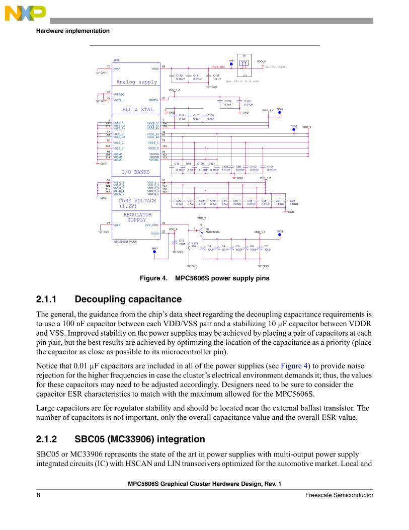
The current application runs at the maximum core speed of 64 MHz. This is one of the main aspects of the design: because of special considerations in the powerup supply (see MPC5606S, MPC5606S Microcontroller Data Sheet for details), a device was selected that provides the power supply that meets these requirements: SBC05 MC33906. Caution needs to be taken, however, to meet the required power consumption, since the MC33906 device can provide only up to 500 mA. Figure 4 shows the power supply schematic used for the design.
NOTEQ2 transistor used does not match with MPC5606S data sheet because the listed components were not available at the time of board construction.
C7 was added to the VDD12 power supply to be able to use different values of capacitance, but 40 µF is the recommended value.
MPC5606S Graphical Cluster Hardware Design, Rev. 1
Freescale Semiconductor 7
Hardware implementation
Figure 4. MPC5606S power supply pins
2.1.1 Decoupling capacitance
The general, the guidance from the chip’s data sheet regarding the decoupling capacitance requirements is to use a 100 nF capacitor between each VDD/VSS pair and a stabilizing 10 µF capacitor between VDDR and VSS. Improved stability on the power supplies may be achieved by placing a pair of capacitors at each pin pair, but the best results are achieved by optimizing the location of the capacitance as a priority (place the capacitor as close as possible to its microcontroller pin).
Notice that 0.01 µF capacitors are included in all of the power supplies (see Figure 4) to provide noise rejection for the higher frequencies in case the cluster’s electrical environment demands it; thus, the values for these capacitors may need to be adjusted accordingly. Designers need to be sure to consider the capacitor ESR characteristics to match with the maximum allowed for the MPC5606S.
Large capacitors are for regulator stability and should be located near the external ballast transistor. The number of capacitors is not important, only the overall capacitance value and the overall ESR value.
2.1.2 SBC05 (MC33906) integration
SBC05 or MC33906 represents the state of the art in power supplies with multi-output power supply integrated circuits (IC) with HSCAN and LIN transceivers optimized for the automotive market. Local and
External supply
C1020.01UF
J6
1 2
C1030.01UF
C1040.01UF
C880.01UF
C910.1uF
C920.1uF
C930.1uF
C940.1uF
R17320K
GND
C800.01UF
C950.01UF
C960.01UF
C970.01UF
C980.01UF
C1070.1uF
DNP
GND
GND
C12
0.10UF
Open SH3 if J6 is used
C1080.1uF
C160.1uF
GND
+ C1910UF
C200.1uF
GND
GND
GNDVDD_3.3
VDD_5
GND
GND
GND
GND
VDD_1.2
GND
VDD_5
VDD_1.2
VDD_5 Q2NJD2873T4
34
1VDD_1.2
VDD_5
+ C310UF
+ C510UF
+ C410UF
+ C710UF
+ C610UF
GND
C1151.0 UF
C99
0.10UF
C1090.1uF
C100
0.10UF
C101
0.10UF
C1100.01UF
TP37
TP38
Analog supply
SUPPLY
CORE VOLTAGE(1.2V)
I/O BANKS
PLL & XTAL
REGULATOR
U1B
SPC5606SF2VLU6
VDDA69
VSSA70
VSSE_A18
VSSE_A2155
VSSE_A3171
VSSE_B147
VSSE_B265
VSSE_C80
VSSE_E134
VSSMA94
VSSMB104
VSSMC114
VDDE_A17
VDDE_A2154
VDDE_A3170
VDDE_B146
VDDE_B264
VDDE_C79
VDDE_E133
VDDMA93
VDDMB103
VDDMC113
VSSOSC28
VSSPLL30
VDDPLL31
VDD12_150
VDD12_267
VDD12_3123
VDD12_4148
VDD12_5163
VSS12_151
VSS12_268
VSS12_3124
VSS12_4149
VSS12_5164
VSSR23
VRC_CTRL25
VDDR22
TP39
TP40
TP41
Vcca_ADC
C1110.01UF
C1120.10UF
MPC5606S Graphical Cluster Hardware Design, Rev. 1
Freescale Semiconductor8
Hardware implementation
bus failure diagnostics, protection, and fail-safe operation mode are provided. The MC3390x family integrates the LIN interface that fulfills LIN protocol specifications 2.0, 2.1, and SAEJ2602-2.
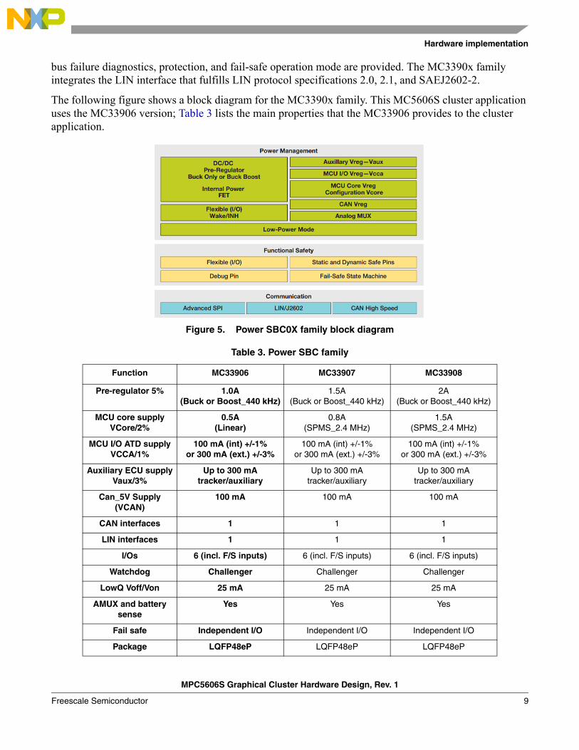
The following figure shows a block diagram for the MC3390x family. This MC5606S cluster application uses the MC33906 version; Table 3 lists the main properties that the MC33906 provides to the cluster application.
Figure 5. Power SBC0X family block diagram
Table 3. Power SBC family
Function MC33906 MC33907 MC33908
Pre-regulator 5% 1.0A(Buck or Boost_440 kHz)
1.5A(Buck or Boost_440 kHz)
2A(Buck or Boost_440 kHz)
MCU core supply VCore/2%
0.5A(Linear)
0.8A(SPMS_2.4 MHz)
1.5A(SPMS_2.4 MHz)
MCU I/O ATD supply VCCA/1%
100 mA (int) +/-1%or 300 mA (ext.) +/-3%
100 mA (int) +/-1%or 300 mA (ext.) +/-3%
100 mA (int) +/-1%or 300 mA (ext.) +/-3%
Auxiliary ECU supply Vaux/3%
Up to 300 mAtracker/auxiliary
Up to 300 mAtracker/auxiliary
Up to 300 mAtracker/auxiliary
Can_5V Supply (VCAN)
100 mA 100 mA 100 mA
CAN interfaces 1 1 1
LIN interfaces 1 1 1
I/Os 6 (incl. F/S inputs) 6 (incl. F/S inputs) 6 (incl. F/S inputs)
Watchdog Challenger Challenger Challenger
LowQ Voff/Von 25 mA 25 mA 25 mA
AMUX and battery sense
Yes Yes Yes
Fail safe Independent I/O Independent I/O Independent I/O
Package LQFP48eP LQFP48eP LQFP48eP
MPC5606S Graphical Cluster Hardware Design, Rev. 1
Freescale Semiconductor 9
Hardware implementation
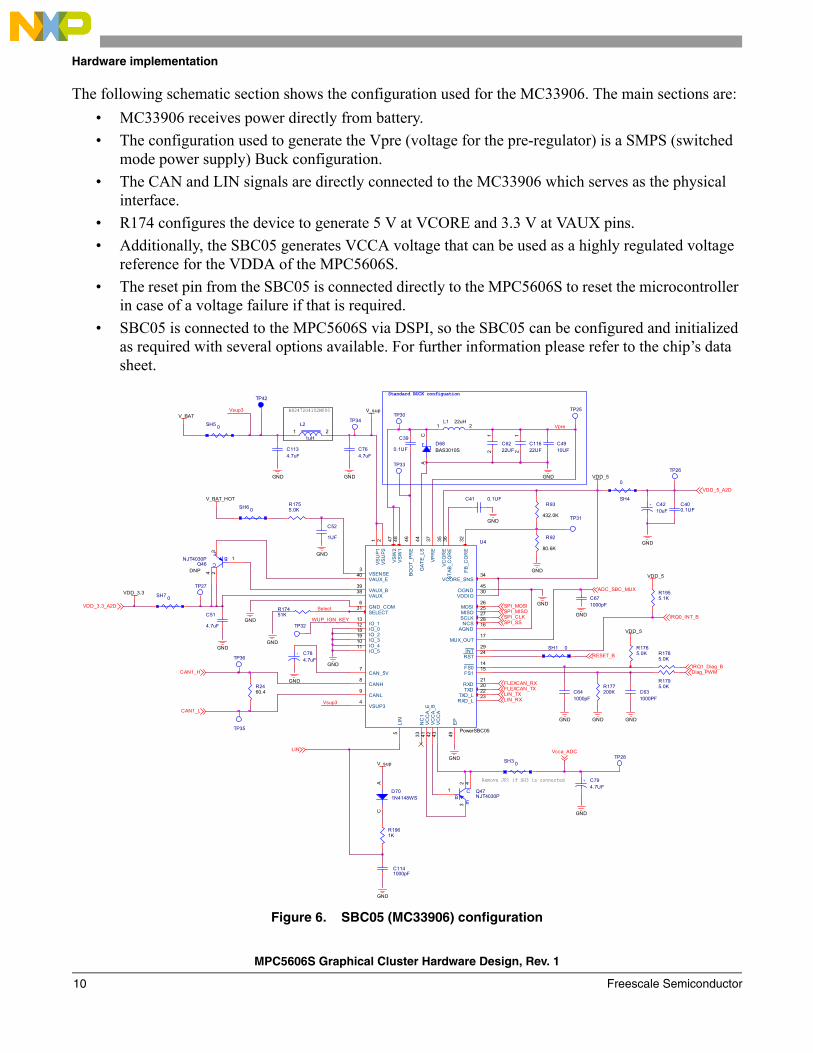
The following schematic section shows the configuration used for the MC33906. The main sections are:
• MC33906 receives power directly from battery.
• The configuration used to generate the Vpre (voltage for the pre-regulator) is a SMPS (switched mode power supply) Buck configuration.
• The CAN and LIN signals are directly connected to the MC33906 which serves as the physical interface.
• R174 configures the device to generate 5 V at VCORE and 3.3 V at VAUX pins.
• Additionally, the SBC05 generates VCCA voltage that can be used as a highly regulated voltage reference for the VDDA of the MPC5606S.
• The reset pin from the SBC05 is connected directly to the MPC5606S to reset the microcontroller in case of a voltage failure if that is required.
• SBC05 is connected to the MPC5606S via DSPI, so the SBC05 can be configured and initialized as required with several options available. For further information please refer to the chip’s data sheet.
Figure 6. SBC05 (MC33906) configuration
GND
+ C794.7UF
TP31
TP32
SH6 0
B82472G4102M000
SH70
TP25
TP26
TP28
TP27
Standard BUCK configuation
R1785.0K
R1795.0K
C4910UF
TP33
R1955.1K
C1134.7uF
VDD_5
C641000pF
C631000PF
GND
EB
C Q47NJT4030P
1
32 4
Vpre
GND
SH3 0
GND
GND
C1141000pF
D701N4148WS
AC
R1961K
GND
SPI_MOSISPI_MISOSPI_CLKSPI_SS
C51
4.7uF
TP34
V_sup
C39
0.1UF
V_sup
C52
1UF
GND
WUP_IGN_KEY
L1 22uH1 2
C400.1UF
C41 0.1UF
GND
C671000pF
+ C784.7uF
GND
SH1 0GND
Vsup3
TP35
TP36
+ C4210uF
VDD_5_A2D
VDD_3.3_A2D
GND
IRQ0_INT_B
GND
GND
RESET_B
GND
CAN1_H
CAN1_L
LIN
GND
R2460.4
GND
Vsup3
L2
1uH1 2
Select
GNDGND
FLEXCAN_TXFLEXCAN_RX
C6222UF
12
LIN_TXLIN_RX
ADC_SBC_MUX
VDD_5
VDD_3.3
U4
PowerSBC05
VS
UP
22
VSENSE3
VAUX_E40
VS
UP
11
VAUX38
VDDIO30VAUX_B
39
GND_COM6
IO_410
IO_511
IO_113
SELECT31
IO_012
IO_218
IO_319
CAN_5V7
CANH8
CANL9
VSUP34
TXD20
VCORE_SNS34
FS014
FS115
MUX_OUT17
RXD_L23
MISO25
SCLK27
MOSI26
NCS28
RXD21
RST24INT29
TXD_L22
NC
133
VC
CA
_E41
VC
CA
_B42
VC
CA
43
BO
OT
_P
RE
46
GA
TE
_L
S4
4
VP
RE
37
VC
OR
E3
5
ST
AB
_CO
RE
36
FB
_CO
RE
32
VS
W2
47
VS
W1
48
LIN
5
AGND16
DGND45
EP
49
R92
80.6K
V_BAT
V_BAT_HOTR93
432.0K
GND
C11622UF
12
Remove JP1 if SH3 is connected
Vcca_ADC
C764.7uF
R17451K
EB
CQ46NJT4030P
DNP
1
324
R1755.0K
R1765.0K
VDD_5
R177200K
GND
TP42
SH4
0
D68BAS3010S
AC
IRQ1_Diag_BDiag_PWM
SH50
TP30
MPC5606S Graphical Cluster Hardware Design, Rev. 1
Freescale Semiconductor10
Hardware implementation
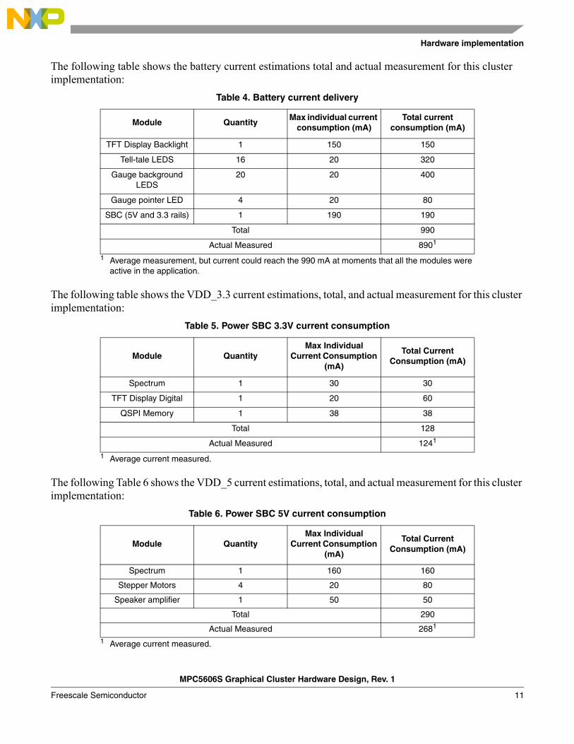
The following table shows the battery current estimations total and actual measurement for this cluster implementation:
The following table shows the VDD_3.3 current estimations, total, and actual measurement for this cluster implementation:
The following Table 6 shows the VDD_5 current estimations, total, and actual measurement for this cluster implementation:
Table 4. Battery current delivery
Module QuantityMax individual current
consumption (mA)Total current
consumption (mA)
TFT Display Backlight 1 150 150
Tell-tale LEDS 16 20 320
Gauge background LEDS
20 20 400
Gauge pointer LED 4 20 80
SBC (5V and 3.3 rails) 1 190 190
Total 990
Actual Measured 8901
1 Average measurement, but current could reach the 990 mA at moments that all the modules were active in the application.
Table 5. Power SBC 3.3V current consumption
Module QuantityMax Individual
Current Consumption (mA)
Total Current Consumption (mA)
Spectrum 1 30 30
TFT Display Digital 1 20 60
QSPI Memory 1 38 38
Total 128
Actual Measured 1241
1 Average current measured.
Table 6. Power SBC 5V current consumption
Module QuantityMax Individual
Current Consumption (mA)
Total Current Consumption (mA)
Spectrum 1 160 160
Stepper Motors 4 20 80
Speaker amplifier 1 50 50
Total 290
Actual Measured 2681
1 Average current measured.
MPC5606S Graphical Cluster Hardware Design, Rev. 1
Freescale Semiconductor 11
Hardware implementation
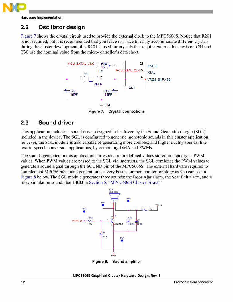
2.2 Oscillator designFigure 7 shows the crystal circuit used to provide the external clock to the MPC5606S. Notice that R201 is not required, but it is recommended that you leave its space to easily accommodate different crystals during the cluster development; this R201 is used for crystals that require external bias resistor. C31 and C30 use the nominal value from the microcontroller’s data sheet.
Figure 7. Crystal connections
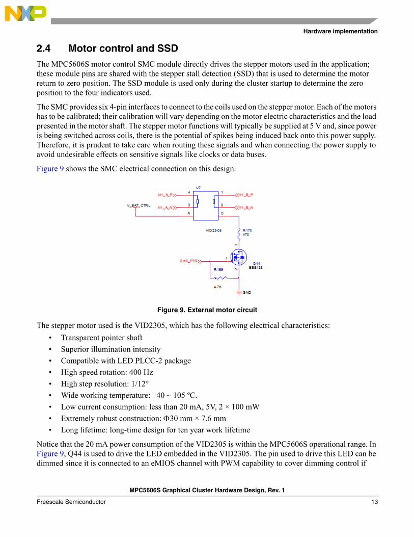
2.3 Sound driverThis application includes a sound driver designed to be driven by the Sound Generation Logic (SGL) included in the device. The SGL is configured to generate monotonic sounds in this cluster application; however, the SGL module is also capable of generating more complex and higher quality sounds, like text-to-speech conversion applications, by combining DMA and PWMs.
The sounds generated in this application correspond to predefined values stored in memory as PWM values. When PWM values are passed to the SGL via interrupts, the SGL combines the PWM values to generate a sound signal through the SOUND pin of the MPC5606S. The external hardware required to complement MPC5606S sound generation is a very basic common emitter topology as you can see in Figure 8 below. The SGL module generates three sounds: the Door Ajar alarm, the Seat Belt alarm, and a relay simulation sound. See ER03 in Section 5, “MPC5606S Cluster Errata.”
Figure 8. Sound amplifier
+
LS3CVS-1508
1 2
VDD_5
SOUND
GND
Q6
MMBT440123
1 +C69
470UF
R192 100
R193
10K
C70
0.01UF
C71
0.01UF
TP44
TP45
TP46
TP47
MPC5606S Graphical Cluster Hardware Design, Rev. 1
Freescale Semiconductor12
Hardware implementation
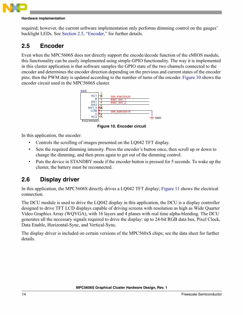
2.4 Motor control and SSDThe MPC5606S motor control SMC module directly drives the stepper motors used in the application; these module pins are shared with the stepper stall detection (SSD) that is used to determine the motor return to zero position. The SSD module is used only during the cluster startup to determine the zero position to the four indicators used.
The SMC provides six 4-pin interfaces to connect to the coils used on the stepper motor. Each of the motors has to be calibrated; their calibration will vary depending on the motor electric characteristics and the load presented in the motor shaft. The stepper motor functions will typically be supplied at 5 V and, since power is being switched across coils, there is the potential of spikes being induced back onto this power supply. Therefore, it is prudent to take care when routing these signals and when connecting the power supply to avoid undesirable effects on sensitive signals like clocks or data buses.
Figure 9 shows the SMC electrical connection on this design.
Figure 9. External motor circuit
The stepper motor used is the VID2305, which has the following electrical characteristics:
• Transparent pointer shaft
• Superior illumination intensity
• Compatible with LED PLCC-2 package
• High speed rotation: 400 Hz
• High step resolution: 1/12°
• Wide working temperature: –40 ~ 105 ºC.
• Low current consumption: less than 20 mA, 5V, 2 × 100 mW
• Extremely robust construction: 30 mm × 7.6 mm
• Long lifetime: long-time design for ten year work lifetime
Notice that the 20 mA power consumption of the VID2305 is within the MPC5606S operational range. In Figure 9, Q44 is used to drive the LED embedded in the VID2305. The pin used to drive this LED can be dimmed since it is connected to an eMIOS channel with PWM capability to cover dimming control if
MPC5606S Graphical Cluster Hardware Design, Rev. 1
Freescale Semiconductor 13
Hardware implementation
required; however, the current software implementation only performs dimming control on the gauges’ backlight LEDs. See Section 2.5, “Encoder,” for further details.
2.5 EncoderEven when the MPC5606S does not directly support the encode/decode function of the eMIOS module, this functionality can be easily implemented using simple GPIO functionality. The way it is implemented in this cluster application is that software samples the GPIO state of the two channels connected to the encoder and determines the encoder direction depending on the previous and current states of the encoder pins; then the PWM duty is updated according to the number of turns of the encoder. Figure 10 shows the encoder circuit used in the MPC5606S cluster.
Figure 10. Encoder circuit
In this application, the encoder:
• Controls the scrolling of images presented on the LQ042 TFT display.
• Sets the required dimming intensity. Press the encoder’s button once, then scroll up or down to change the dimming, and then press again to get out of the dimming control.
• Puts the device in STANDBY mode if the encoder button is pressed for 5 seconds. To wake up the cluster, the battery must be reconnected.
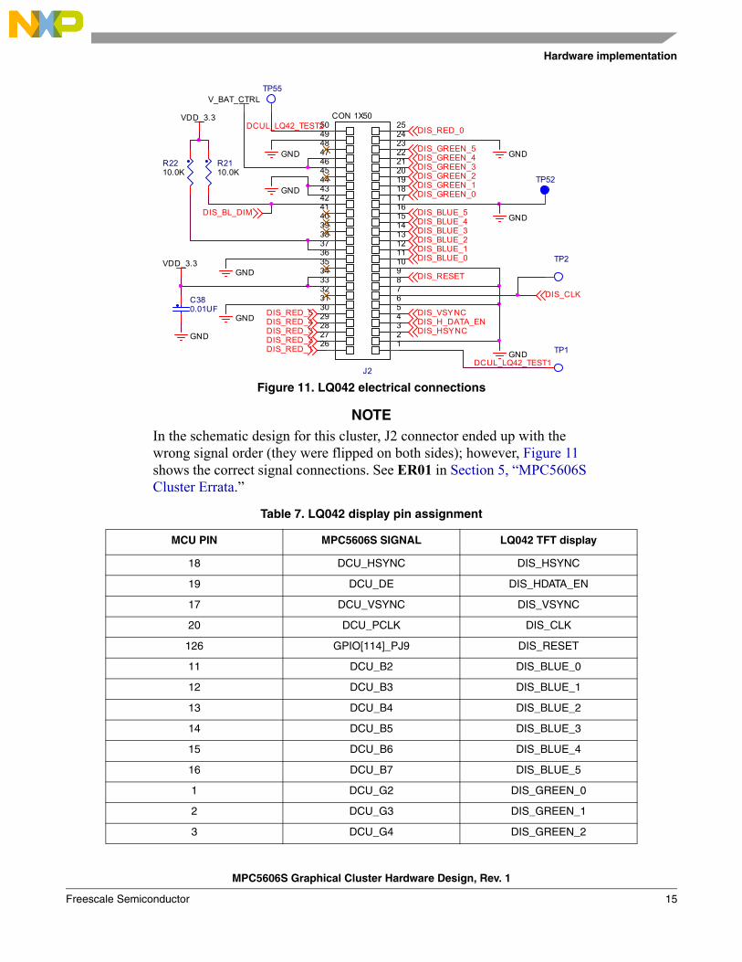
2.6 Display driverIn this application, the MPC5606S directly drives a LQ042 TFT display; Figure 11 shows the electrical connection.
The DCU module is used to drive the LQ042 display in this application, the DCU is a display controller designed to drive TFT LCD displays capable of driving screens with resolution as high as Wide Quarter Video Graphics Array (WQVGA), with 16 layers and 4 planes with real time alpha-blending. The DCU generates all the necessary signals required to drive the display: up to 24-bit RGB data bus, Pixel Clock, Data Enable, Horizontal-Sync, and Vertical-Sync.
The display driver is included on certain versions of the MPC560xS chips; see the data sheet for further details.
SW8
EVQ-WKA001
SW1_55
B2
SW13
SW24
NC11
COM6
A7
NC28
ENC_SW_1ENC_SW_2
SW_EMIOSA19
GND
SW_EMIOSA20
MPC5606S Graphical Cluster Hardware Design, Rev. 1
Freescale Semiconductor14
Hardware implementation
Figure 11. LQ042 electrical connections
NOTEIn the schematic design for this cluster, J2 connector ended up with the wrong signal order (they were flipped on both sides); however, Figure 11 shows the correct signal connections. See ER01 in Section 5, “MPC5606S Cluster Errata.”
Table 7. LQ042 display pin assignment
MCU PIN MPC5606S SIGNAL LQ042 TFT display
18 DCU_HSYNC DIS_HSYNC
19 DCU_DE DIS_HDATA_EN
17 DCU_VSYNC DIS_VSYNC
20 DCU_PCLK DIS_CLK
126 GPIO[114]_PJ9 DIS_RESET
11 DCU_B2 DIS_BLUE_0
12 DCU_B3 DIS_BLUE_1
13 DCU_B4 DIS_BLUE_2
14 DCU_B5 DIS_BLUE_3
15 DCU_B6 DIS_BLUE_4
16 DCU_B7 DIS_BLUE_5
1 DCU_G2 DIS_GREEN_0
2 DCU_G3 DIS_GREEN_1
3 DCU_G4 DIS_GREEN_2
DIS_BL_DIM
TP1
DCUL_LQ42_TEST1
TP55
J2
CON 1X50
12345678910
1211
13141516171819202122232425
26272829303132333435363738394041424344454647484950
V_BAT_CTRL
GND
DCUL_LQ42_TEST2
GND
TP2
R2110.0K
VDD_3.3
R2210.0K
GNDVDD_3.3
C380.01UF
GND
GNDDIS_RED_5DIS_RED_4
DIS_RED_2DIS_RED_3
DIS_RED_1
DIS_RED_0
GNDDIS_GREEN_5
DIS_GREEN_3DIS_GREEN_4
DIS_GREEN_2
DIS_GREEN_0DIS_GREEN_1
GNDDIS_BLUE_5
DIS_BLUE_3DIS_BLUE_4
DIS_BLUE_1DIS_BLUE_0
DIS_BLUE_2
GND
DIS_RESET
DIS_CLK
DIS_VSYNCDIS_H_DATA_ENDIS_HSYNC
TP52
MPC5606S Graphical Cluster Hardware Design, Rev. 1
Freescale Semiconductor 15
Hardware implementation
Note: DCU_LQ42-TEST1/2 not connected to MCU and is only for LQ042 test purposes.
Note: See ER01 in Section 5, “MPC5606S Cluster Errata,” for cautions on the LQ042 connections.
Depending on the operating environment, it may also be important to consider the location and operating frequency of the display to be driven by the device. It is typical for the panel to be connected directly to the same board as the MPC5606S; however, if the panel must be at a greater distance, then the drive strength of the MCU pins must be considered. Similarly, a fast clock rate for a panel may require a higher drive strength capability for the pins which may in turn cause impedance matching problems with the panel.
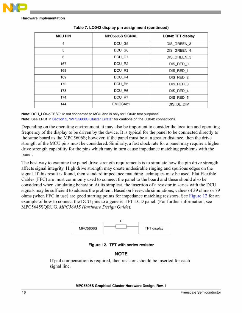
The best way to examine the panel drive strength requirements is to simulate how the pin drive strength affects signal integrity. High drive strength may create undesirable ringing and spurious edges on the signal. If this result is found, then standard impedance matching techniques may be used. Flat Flexible Cables (FFC) are most commonly used to connect the panel to the board and these should also be considered when simulating behavior. At its simplest, the insertion of a resistor in series with the DCU signals may be sufficient to address the problem. Based on Freescale simulations, values of 39 ohms or 79 ohms (when FFC in use) are good starting points for impedance matching resistors. See Figure 12 for an example of how to connect the DCU pins to a generic TFT LCD panel. (For further information, see MPC5645SQRUG, MPC5645S Hardware Design Guide).
Figure 12. TFT with series resistor
NOTEIf pad compensation is required, then resistors should be inserted for each signal line.
4 DCU_G5 DIS_GREEN_3
5 DCU_G6 DIS_GREEN_4
6 DCU_G7 DIS_GREEN_5
167 DCU_R2 DIS_RED_0
168 DCU_R3 DIS_RED_1
169 DCU_R4 DIS_RED_2
172 DCU_R5 DIS_RED_3
173 DCU_R6 DIS_RED_4
174 DCU_R7 DIS_RED_5
144 EMIOSA21 DIS_BL_DIM
Table 7. LQ042 display pin assignment (continued)
MCU PIN MPC5606S SIGNAL LQ042 TFT display
MPC5606S TFT display
R
MPC5606S Graphical Cluster Hardware Design, Rev. 1
Freescale Semiconductor16
Hardware implementation
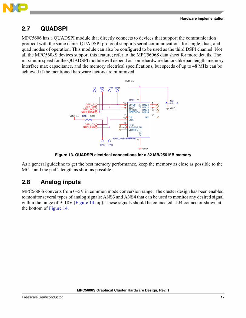
2.7 QUADSPIMPC5606 has a QUADSPI module that directly connects to devices that support the communication protocol with the same name. QUADSPI protocol supports serial communications for single, dual, and quad modes of operation. This module can also be configured to be used as the third DSPI channel. Not all the MPC560xS devices support this feature; refer to the MPC5606S data sheet for more details. The maximum speed for the QUADSPI module will depend on some hardware factors like pad length, memory interface max capacitance, and the memory electrical specifications, but speeds of up to 48 MHz can be achieved if the mentioned hardware factors are minimized.
Figure 13. QUADSPI electrical connections for a 32 MB/256 MB memory
As a general guideline to get the best memory performance, keep the memory as close as possible to the MCU and the pad’s length as short as possible.
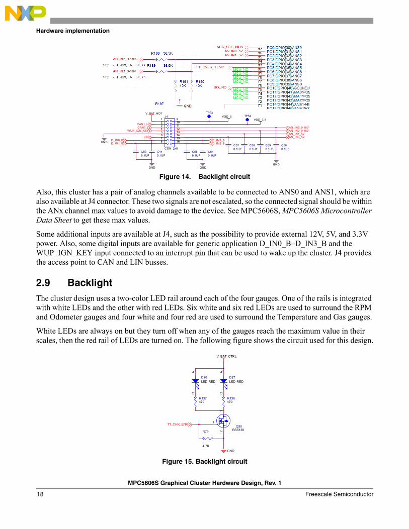
2.8 Analog inputsMPC5606S converts from 0–5V in common mode conversion range. The cluster design has been enabled to monitor several types of analog signals: ANS3 and ANS4 that can be used to monitor any desired signal within the range of 9–18V (Figure 14 top). These signals should be connected at J4 connector shown at the bottom of Figure 14.
QSPI_HOLDQSPI_ACC
QSPI_CSQSPI_SCK
QSPI_SOQSPI_SI
GND
VDD_3.3
C340.01UF
GND
R18 100KVDD_3.3
U10
S25FL256SDPMFV011
HOLD/IO31
VC
C2
CS7
WP/IO29
VS
S10
NC13
VIO/RFU14
SCK16
DNU14
DNU25
DNU311
DNU412
SO/IO18 SI/IO0
15
RFU6
RESET/RFU3
TP9TP8 TP11TP10
TP12 TP13
MPC5606S Graphical Cluster Hardware Design, Rev. 1
Freescale Semiconductor 17
Hardware implementation
Figure 14. Backlight circuit
Also, this cluster has a pair of analog channels available to be connected to ANS0 and ANS1, which are also available at J4 connector. These two signals are not escalated, so the connected signal should be within the ANx channel max values to avoid damage to the device. See MPC5606S, MPC5606S Microcontroller Data Sheet to get these max values.
Some additional inputs are available at J4, such as the possibility to provide external 12V, 5V, and 3.3V power. Also, some digital inputs are available for generic application D_IN0_B–D_IN3_B and the WUP_IGN_KEY input connected to an interrupt pin that can be used to wake up the cluster. J4 provides the access point to CAN and LIN busses.
2.9 BacklightThe cluster design uses a two-color LED rail around each of the four gauges. One of the rails is integrated with white LEDs and the other with red LEDs. Six white and six red LEDs are used to surround the RPM and Odometer gauges and four white and four red are used to surround the Temperature and Gas gauges.
White LEDs are always on but they turn off when any of the gauges reach the maximum value in their scales, then the red rail of LEDs are turned on. The following figure shows the circuit used for this design.
Figure 15. Backlight circuit
VDD_5VDD_3.3
GND
V_BAT_HOT TP53TP54
CAN1_HCAN1_L
WUP_IGN_KEY
LIND_IN0_BD_IN1_B
AN_IN3_9-18VAN_IN2_9-18VAN_IN1_5VAN_IN0_5V
D_IN2_BD_IN3_B
C440.1UF
GND
C530.1UF
C540.1UF
GND
C550.1UF
J4
CON_2x8
12345678
910111213141516
C560.1UF
C570.1UF
C590.1UF
C580.1UF
GND
GND
Q30BSS138
1
23
D26LED RED
AC
V_BAT_CTRL
R79
4.7K
TT_CHK_ENG
D27LED RED
AC
R137470
R138470
MPC5606S Graphical Cluster Hardware Design, Rev. 1
Freescale Semiconductor18
Conclusion
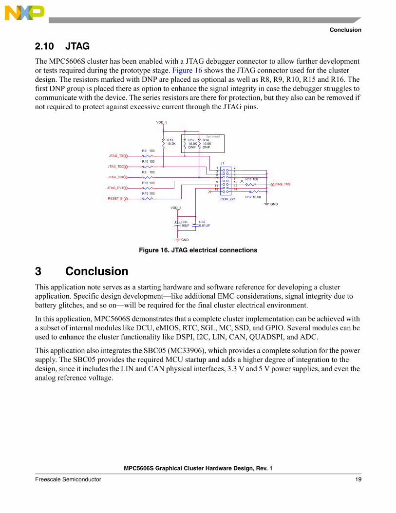
2.10 JTAGThe MPC5606S cluster has been enabled with a JTAG debugger connector to allow further development or tests required during the prototype stage. Figure 16 shows the JTAG connector used for the cluster design. The resistors marked with DNP are placed as optional as well as R8, R9, R10, R15 and R16. The first DNP group is placed there as option to enhance the signal integrity in case the debugger struggles to communicate with the device. The series resistors are there for protection, but they also can be removed if not required to protect against excessive current through the JTAG pins.
Figure 16. JTAG electrical connections
3 ConclusionThis application note serves as a starting hardware and software reference for developing a cluster application. Specific design development—like additional EMC considerations, signal integrity due to battery glitches, and so on—will be required for the final cluster electrical environment.
In this application, MPC5606S demonstrates that a complete cluster implementation can be achieved with a subset of internal modules like DCU, eMIOS, RTC, SGL, MC, SSD, and GPIO. Several modules can be used to enhance the cluster functionality like DSPI, I2C, LIN, CAN, QUADSPI, and ADC.
This application also integrates the SBC05 (MC33906), which provides a complete solution for the power supply. The SBC05 provides the required MCU startup and adds a higher degree of integration to the design, since it includes the LIN and CAN physical interfaces, 3.3 V and 5 V power supplies, and even the analog reference voltage.
R8 100
JTAG_TDO
JTAG_TDI
JTAG_TCK
JTAG_TMS
R9 100
R10 100
R11 100
J1
CON_2X7
1 23 4
657 89 10
11 1213 14
R1210.0KDNP
VDD_5
R1310.0K
R1410.0KDNP
RESET_B
R15 100
VDD_5
C320.01UF
+ C3310UF
GND
GND
JTAG_EVTI
R16 100
R17 10.0K
Optional
MPC5606S Graphical Cluster Hardware Design, Rev. 1
Freescale Semiconductor 19
References
4 References
5 MPC5606S Cluster ErrataThe following errata are only for this hardware implementation and are not related in any way to the MPC5606S chip errata.
6 AcknowledgementsI would like to thank all the support given by my local team in Mexico and the support given by the FAE team during the cluster design reviews.
Document number Title Availability
MPC5645SQRUG MPC5645S Hardware Design Guide freescale.com
MPC5606SRM MPC5606S Microcontroller Reference Manual
MPC5606S MPC5606S Microcontroller Data Sheet
AN4442 Integrating the MPC5643L and MC33907/08 for Safety Applications
MC33906_7_8FS MC33906/07/08 Fact Sheet
Item number Description
ER01 LQ042 display connector was installed with the signals flipped on both sides.
WA01 A twisted flex cable was used to fix this issue.
ER02 TP54 and TP40 present discontinuity.
WA02 TP54 and TP40 must be shorted for VDD_3.3 signal.
ER03 LS2 polarized buzzer used in place of a speaker.
WA03 Speaker used to replace the LS2 buzzer.
ER04 Q46 missing in the design.
WA04 Q46 installed in cluster board even when marked as DNP (do not populate in the design).
MPC5606S Graphical Cluster Hardware Design, Rev. 1
Freescale Semiconductor20

THIS PAGE IS INTENTIONALLY BLANK
MPC5606S Graphical Cluster Hardware Design, Rev. 1
Freescale Semiconductor 21
Document Number: AN4719Rev. 104/2013
Information in this document is provided solely to enable system and software
implementers to use Freescale products. There are no express or implied copyright
licenses granted hereunder to design or fabricate any integrated circuits based on the
information in this document.
Freescale reserves the right to make changes without further notice to any products
herein. Freescale makes no warranty, representation, or guarantee regarding the
suitability of its products for any particular purpose, nor does Freescale assume any
liability arising out of the application or use of any product or circuit, and specifically
disclaims any and all liability, including without limitation consequential or incidental
damages. “Typical” parameters that may be provided in Freescale data sheets and/or
specifications can and do vary in different applications, and actual performance may
vary over time. All operating parameters, including “typicals,” must be validated for each
customer application by customer’s technical experts. Freescale does not convey any
license under its patent rights nor the rights of others.
How to Reach Us:
Home Page: freescale.com
Web Support: freescale.com/support
Freescale and the Freescale logo are trademarks of Freescale Semiconductor, Inc. All
other product or service names are the property of their respective owners. The Power
Architecture and Power.org word marks and the Power and Power.org logos and
related marks are trademarks and service marks licensed by Power.org.
© 2013 Freescale Semiconductor, Inc.