Embed Size (px)
Citation preview

1
On-chip thermal testing using MOSFETs in weak
inversion
Authors: Ferran Revertera and Josep Altetb
Address: Department of Electronic Engineering Universitat Politècnica de Catalunya (UPC) – BarcelonaTech a C/ Esteve Terradas 7, C4, 08860 Castelldefels (Barcelona), Spain
b C/ Jordi Girona 1-3, Campus Nord, C4, 08034 Barcelona, Spain
Corresponding author: Ferran Reverter, [email protected] Phone: +34 934137076
Telefax: +34 934137007

2
Abstract—This paper analyses the feasibility of using metal-oxide-semiconductor field-effect
transistors (MOSFET) operating in weak inversion as temperature sensors for on-chip thermal
testing applications. MOSFETs in weak inversion are theoretically analyzed so as to know
how their sensitivity to temperature depends on both dimensions and bias current. Theoretical
predictions are then compared with simulations and experimental data resulting from
MOSFETs fabricated in a commercial 0.35 μm CMOS technology. MOSFETs are
experimentally subjected to changes of temperature generated by either a heating chamber or
an on-chip power dissipating device. The performance of MOSFETs in weak inversion is also
compared with that in strong inversion and with that of parasitic bipolar junction transistors
(BJT). In the context of on-chip thermal testing, MOSFETs in weak inversion offer
advantages in terms of layout area, linearity, current consumption and spread of the sensitivity
to temperature due to process variations.
Keywords: MOSFET sensor; Subthreshold operation; Temperature sensor; Thermal testing;
Weak inversion.

3
I. INTRODUCTION
Thermal testing and characterization of integrated circuits (IC), e.g. digital circuits [1, 2]
and analogue radio frequency (RF) circuits [3, 4], through temperature sensors embedded into
the same chip has been proved useful in the last years. The temperature sensor is placed close
to the circuit under test (CUT) and measures on-chip thermal variations caused by the power
dissipated by the CUT with the aim of extracting information, for example: (i) the efficiency
(i.e. the DC power dissipated by the load divided by the DC power delivered by the DC
source) of a RF power amplifier operating at 2 GHz [3], and (ii) the frequency response and
the central frequency (at 830 MHz) of a RF low-noise amplifier [4]. In comparison with
classical IC test techniques based on electrical measurements [5-7], thermal testing offers two
main advantages for RF-ICs: the CUT is not electrically loaded, and measurements are
performed at DC [3] or at low frequency [4, 8], which reduces the complexity and cost of the
test.
On-chip thermal testing of RF-CUTs has been performed in [3, 4] using the well-known
temperature dependence (i.e. –2 mV/K) of the base-emitter voltage of a parasitic BJT
fabricated in CMOS technology [9]. However, the comparative analysis carried out in [10]
shows that MOSFET-based temperature sensors (operating in strong inversion) offer
attractive advantages for such applications: (i) fully compatibility with the fabrication process,
(ii) less layout area (say, ten times less) required around the CUT, and (iii) more sensitivity
(up to three times more) to on-chip thermal variations caused by the CUT. The main
drawback of MOSFETs is that their sensitivity to temperature is more susceptible (say, four
times more) to IC manufacturing process variations [10].
This paper goes a step further in the analysis of MOSFETs as temperature sensors for on-
chip thermal testing applications. The approach proposed in [10] is applied herein to analyze
the feasibility of using MOSFETs in weak inversion, instead of strong inversion, as

4
temperature sensors for such applications. Although MOSFETs in weak inversion have been
already proposed as low-power temperature sensors [2, 11, 12], no comparative analysis (with
respect to BJTs and MOSFETs in strong inversion) has been carried out in the context of on-
chip thermal testing. After explaining the IC thermal testing technique behind the proposed
temperature sensor, this paper provides theoretical models, simulations and experimental
results of MOSFETs operating in weak inversion, and then it compares these results with
those reported in [10] with the purpose of extracting the advantages and drawbacks of each
sensing transistor.
II. ON-CHIP THERMAL TESTING TECHNIQUE
The temperature sensor analyzed herein is mainly intended for the on-chip thermal
characterization of RF circuits using the heterodyne technique [4]. This technique operates as
follows: two tones of high frequency f1 and f2 = f1 + Δf (Δf being, for instance, 1 kHz) are
applied to the input of the RF-CUT (see Fig. 1a) and, as a consequence of the frequency
mixing generated by Joule effect [13], the RF-CUT dissipates power at low frequency (i.e. at
Δf) with information about the performance at high frequency (i.e. at f1). Accordingly, the
frequency response of a RF-CUT can be achieved by monitoring the amplitude of the power
dissipated at Δf for different values of f1 [4]. This power dissipated at Δf generates an on-chip
temperature signal at the same frequency that can be measured by a nearby temperature
sensor (T1 in Fig. 1a) that is thermally coupled to the CUT through the semiconductor
substrate; note that the low-pass filter response of the thermal coupling filters out other
spectral components of the dissipated power (such as those at f1, f2, f1 + f2,…). The
temperature sensor is then proposed to be connected to an amplifying band-pass filter (BPF)
whose passband is centered at Δf so as to limit the bandwidth (and, hence, the noise) around
the frequency of interest [8]. The BPF also rejects slow variations of the ambient temperature
affecting the IC, and slow variations of on-chip temperature generated by the DC bias of the

5
CUT or by any other heating source.
The simplest temperature sensor that can be employed in Fig. 1a is a diode-connected
MOSFET biased with a constant current source (IB), as shown in Fig. 1b [8, 10]. In this
circuit, the MOSFET carries out a small-signal temperature-to-voltage conversion at low
frequency (i.e. at Δf) with the aim of extracting high-frequency information of the RF-CUT.
Although the DC operating point of that circuit is quite susceptible to process variations, this
is not a major concern since the DC level (and, hence, the corresponding absolute value of
temperature) will be blocked out by the ensuing BPF shown in Fig. 1a. What it really matters
here is the measurement of the temperature change at Δf generated by the RF-CUT when the
heterodyne technique is applied. For this reason, next sections mainly focus on the ability of
the sensor to detect changes of temperature (i.e. the sensitivity to temperature) rather than the
accuracy. The amplitude of the temperature change to be detected depends on several factors
(such as the operating frequency, the dissipated power, and the distance between the CUT and
the temperature sensor), but values around tenths [8] or a few units of Kelvin [13] are
expected. In the literature, we can find other thermal applications interested in measuring
changes of temperature rather than the absolute value of temperature. For instance, the
measurement of the amplitude (and also the phase shift) of temperature oscillations at a given
frequency generated by the AC power dissipated by a heating element is used to determine
thermal properties of fluids [14] and to monitor biofilm dynamics [15].
III. THEORETICAL ANALYSIS
This section analyses the same MOSFET-based temperature sensor proposed in [10] (i.e. a
diode-connected n-type MOSFET biased with IB, as shown in Fig. 1b) but in weak inversion
(or subthreshold) operation. For the application of interest described in Section II, the current
source IB will be far from and, hence, not affected by the power dissipated by the CUT and,
for this reason, IB is assumed to be constant in the following analysis. Of course, IB could be
6
affected by changes of ambient temperature, but such effects are not expected to be critical
here whenever the IC test is faster than the temperature changes affecting IB.
In weak inversion (i.e. VGS < VTH) and in saturation (i.e. VDS > 5UT), the current-voltage
characteristic of a MOSFET can be modeled as follows [16]
2 GS THD OX T
T
( 1) exp V VWI C UL U
μ ηη
⎛ ⎞−= − ⎜ ⎟⎝ ⎠
, (1)
where ID is the drain current, VGS is the gate-source voltage, VDS is the drain-source voltage,
W is the channel width, L is the channel length, VTH is the threshold voltage, µ is the carriers
mobility, UT is the thermal voltage, η is a subthreshold slope factor, COX (= εOX/tOX) is the
gate oxide capacitance per unit area, εOX is the gate oxide permittivity, and tOX is the gate
oxide thickness. Unlike what happens in strong inversion where the current-voltage
characteristic has a quadratic relationship [10], in weak inversion the relationship is
exponential, as in BJTs; this is because in weak inversion the channel current flows by
diffusion [17].
According to [18], three parameters involved in (1) depend on temperature:
T ( ) kTU Tq
= (2)
00
( ) TTT
α
μ μ⎛ ⎞
= ⎜ ⎟⎝ ⎠
(3)
TH TH0 0( ) ( )V T V T Tβ= + − , (4)
where T is the absolute temperature, T0 is a reference temperature (e.g. 300 K), k is the
Boltzmann constant (1.38066·10-23 J/K), q is the elementary charge (1.60218·10-19 C), µ0 is
the carriers mobility at T0, α is a constant generally between –1.5 and –2, VTH0 is the threshold
voltage at T0, and β is a negative temperature coefficient; the value of such parameters for the

7
CMOS technology applied herein is reported in Table I [19]. Note that α and β are negative,
so both µ and VTH decrease with temperature.
For the circuit shown in Fig. 1b where the MOSFET is biased with ID = IB, the output
voltage (which is equal to VGS) can be expressed, from (1), as
Bo T TH
2OX T
ln( 1)
IV U VWC UL
ημ η
⎛ ⎞⎜ ⎟
= +⎜ ⎟⎜ ⎟−⎝ ⎠
. (5)
Replacing now (2), (3) and (4) in (5) yields the temperature dependence of Vo
( ) ( ) 0o TH0 0 T( ) 2 ln TV T V T T U
Tβ β γ α η= − + + + + , (6)
where
B
20 OX T0
ln( 1)
IkWq C UL
γ ημ η
⎛ ⎞⎜ ⎟
= ⎜ ⎟⎜ ⎟−⎝ ⎠
, (7)
UT0 being the thermal voltage at T0 (i.e. 26 mV). Assuming (T0/T) ≈ 1, the logarithmic
function involved in (6) can be replaced by its first-order Taylor-series approximation, i.e.
( )0 0ln 1T T T T≈ − . Consequently, Eq. (6) can be simplified to the following first-order
temperature-dependent equation
( ) ( )o TH0 0 T0( ) 2 2 kV T V T U Tq
β α η β γ α η⎛ ⎞≈ − + + + + − +⎜ ⎟
⎝ ⎠, (8)
whose sensitivity to temperature is
( )oT 2V kS
T qβ γ α η∂= = + − +
∂. (9)
Taking into account that k/q has a low value (i.e. 86 µV/K) and α is close to −2, the last term
in (9) turns to be much smaller than the others and, therefore, ST can be approximated to

8
TS β γ≈ + . (10)
A MOSFET operating in weak inversion requires a high W/L and a low IB [20, 21], so the
term inside the logarithm in (7) is expected to be smaller than one and, hence, γ will be
smaller than zero. Therefore, both β and γ are negative temperature coefficients and,
consequently, the value of ST resulting from (10) will be also negative. According to (7),
higher values of |γ| (and, hence, of |ST|) can be achieved by operating deeper in weak
inversion, i.e. higher values of W/L and/or lower values of IB; these recommendations are
opposite to those obtained in strong inversion [10]. Table II reports, for different MOSFETs
biased with IB = 10 nA, the theoretical value of ST calculated by (10) using the technology
information provided in Table I and assuming η = 1.5 [22]. Note that the values of ST in weak
inversion are not expected to be as high as those obtained in strong inversion [10] for a
similar layout area occupied by the sensor.
The spread (or variability) of ST (i.e. ΔST) due to IC manufacturing process variations can
be evaluated by applying the law of propagation of uncertainties [23] in (10), thus resulting
in:
2 222 2 2
2 20 OXBT
B 0 OX
tIk W LSq W L I t
μη βμ
⎛ ⎞⎛ ⎞ ⎛ ⎞⎛ ⎞⎛ ⎞ Δ ΔΔΔ Δ⎛ ⎞ ⎛ ⎞⎜ ⎟Δ = + + + + + Δ⎜ ⎟ ⎜ ⎟⎜ ⎟⎜ ⎟ ⎜ ⎟ ⎜ ⎟⎜ ⎟⎝ ⎠ ⎝ ⎠⎝ ⎠ ⎝ ⎠ ⎝ ⎠ ⎝ ⎠⎝ ⎠, (11)
where ΔW, ΔL, ΔIB, Δµ0, ΔtOX and Δβ are, respectively, the spread (or variability) of W, L, IB,
µ0, tOX and β due to process variations. As in [10], ΔST depends on the relative variability of
W, L, IB, µ0 and tOX, but here these are multiplied by ηk/q, which is a small value (129 µV/K
for η = 1.5). For example, if the quadratic sum of the relative variability of W, L, IB, µ0 and
tOX equals 10 %, then the resulting value of ΔST equals 12.9 µV/K, which is less than 1 % of
the nominal values of ST reported in Table II. Accordingly, MOSFETs with a high W and/or a
high L are not expected to carry major benefits in terms of spread of ST when operating in

9
weak inversion, although they do in strong inversion [10]. On the other hand, the term Δβ is
usually neglected [24] but here its effects on ΔST could be comparable to those discussed
before.
As explained in Section II, the change of temperature (ΔT) to be detected by the
MOSFET sensor shown in Fig. 1b is to be caused by a change of power (ΔP) dissipated by
the CUT. Consequently, the change of the sensor output voltage (ΔVo) can be expressed as a
function of ΔP as
o T T th PV S T S R P S PΔ = Δ = Δ = Δ , (12)
where Rth is a thermal coupling resistance that relates the change of temperature at the
MOSFET sensor to the change of power dissipated by the CUT, and SP is the sensitivity of the
sensor to the power dissipated, which depends on both ST and Rth.
IV. SIMULATION RESULTS
The temperature sensor shown in Fig. 1b has been simulated with Cadence in 0.35 µm
CMOS technology of AMS (AustriaMicroSystems) with VDD = 3.3 V and using BSIM3v3
models. Table II summarizes the dimensions of the MOSFETs simulated, which have a high
W/L so as to increase the sensitivity to temperature, as suggested by (7) and (10). The
temperature dependence of such MOSFETs has been simulated through a DC temperature-
sweep analysis assuming 300 K (27 ºC) as a reference (i.e. ΔT = T – 300 K).
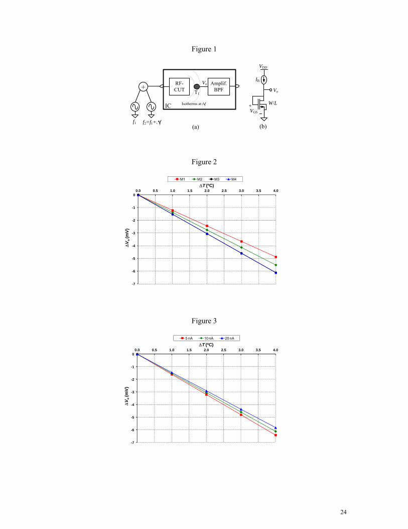
Figure 2 shows how the output voltage of the sensor in Fig. 1b depends on temperature for
different MOSFET dimensions when IB = 10 nA. For such dimensions, the output voltage
decreases linearly with temperature, as predicted by (8). Furthermore, ST increases (in
absolute value) with the factor W/L, as expected from (7). MOSFETs M3 and M4, which have
different values of W and L but the same W/L, show almost the same temperature dependence,
as also expected from (7). The value of ST of each of the cases represented in Fig. 2 and the
corresponding value normalized to the maximum sensitivity (i.e. that of M3 or M4) are

10
summarized in Table II. Note that the values of ST resulting from simulations are very similar
(differences are smaller than 10 %) to those calculated by (10) and, therefore, the models
developed in Section III seem to be useful for a first estimation of ST.
Figure 3 shows how the output voltage of M3 depends on temperature for different bias
currents (5 nA, 10 nA, and 20 nA). For the three currents simulated, the output voltage
decreases linearly with temperature, as predicted by (8). In addition, as suggested by (7), |ST|
decreases with IB; to be precise: ST equals −1.602 mV/K, −1.529 mV/K and −1.455 mV/K for
5 nA, 10 nA, and 20 nA, respectively. Note that decreasing IB by a factor of 4 (e.g. from
20 nA to 5 nA) or increasing W/L by a factor of 4 (e.g. from M1 to M2, or from M2 to M3)
brings about the same increase in |ST| (around 150 µV/K in the previous examples).
The effects of process variations on ST have been simulated through a Monte Carlo
analysis of 50 runs. Assuming one standard deviation of ST as ΔST, we have ΔST ≈ 10 µV/K
for the different MOSFET dimensions simulated. Taking into account the values of ST
provided in Table II, the resulting ΔST/ST is smaller than 1 %, which is quite similar to that
obtained with BJTs [10]. Note, however, that the Monte Carlo analysis assumes the spread
due to process variations of some parameters (e.g. W, L, µ0, tOX and VTH0) but not of others
(such as α and β) and, therefore, the previous simulation results of ΔST/ST could be too
optimistic.
The sensor in Fig. 1b has also been simulated over the industrial temperature range (i.e.
from −40 ºC to 85 ºC) with the aim of evaluating how ST depends on the operating
temperature (note that in Figs. 2 and 3, it is assumed to be 27 ºC). The relative change of ST
(calculated as ( )T T T( ) (27º C) (27º C)S T S S− ) versus the operating temperature for different
MOSFETs biased with IB = 10 nA is represented in Fig. 4. Such simulations show that ST
undergoes a very small change (e.g. the change is smaller than 1 % for M2, M3 and M4) and,
therefore, the linear thermal response modeled by (8) seems to be applicable in the industrial

11
temperature range. In comparison with the performance in strong inversion [10], MOSFETs
in weak inversion offer a value of ST that is more independent (up to ten times more) of the
operating temperature and, consequently, they offer more linearity. Simulations have also
shown that the effects of leakage currents coming from reverse-biased pn junctions (such as
the drain-bulk junction) on the temperature dependence of the MOSFET are negligible, at
least for temperatures lower than 85 ºC; for instance, the leakage current of the drain-bulk
junction is around 10 pA at 85 ºC for M4, which is a thousand times smaller than the bias
current (i.e. 10 nA).
V. EXPERIMENTAL RESULTS
A chip including MOSFET-based temperature sensors with the topology shown in Fig. 1b
and with different values of W/L (those listed in Table II) has been implemented in 0.35 µm
2P4M (2 levels of poly, 4 levels of metal) CMOS technology of AMS. The designed chip also
includes heaters that are placed at 5 µm from each of the sensors, as shown in Fig. 5a, with
the purpose of testing the capability of the sensors to monitor on-chip thermal variations
caused by the power dissipated by other embedded circuits; the device used as a heater is
another diode-connected n-type MOSFET with Wh = 450 µm, Lh = 1 µm and 15 fingers. Two
additional blocks have been embedded into the chip (see Fig. 5b): (a) a current mirror that
converts an external current (Iext) from microampere to nanoampere range, and (b) an opamp-
based voltage follower that avoids the loading effects of external instrumentation. This opamp
has (i) an input common mode voltage with a minimum value of 200 mV, which enables us to
read the low voltage coming from the MOSFETs in weak inversion, and (ii) a maximum input
offset voltage (VIO) of 2 mV, whose effects are not expected to be critical here since we will
represent the change of voltage with respect to that obtained at the beginning of the test (i.e. at
ΔT = 0 or ΔP = 0). Furthermore, note that the MOSFET sensor is close to the heater (at 5 µm)
and its sensitivity is around 1-2 mV/K, whereas the opamp (and also the current mirror) is far
12
from the heater (more than 200 µm) and the temperature coefficient of VIO is much lower
(typical values are 1-10 µV/K). Consequently, the effects of the dissipated power on VIO (or
other non-idealities of the opamp) are expected to be much lower than those on the sensor.
The temperature sensors have been initially tested by means of a heating chamber
(MEMMERT, type UM-100), as shown in Fig. 5c; in this experiment, the embedded heaters
did not dissipate power. A bench-top DC current source (Advantest R6240A) provided a
stable Iext that was converted to the nanoampere range through the on-chip current mirror,
whereas a digital multimeter (HP 34401A) measured the output (Vo) of the voltage follower.
Moreover, the actual value of temperature inside the chamber was monitored by a reference
temperature sensor (Pt100 IEC-751 Class A) whose value was measured by another digital
multimeter (HP 3458A) applying the four-wire measurement method. Using this set-up, the
output voltage of different MOSFETs biased with IB = 10 nA was measured at different
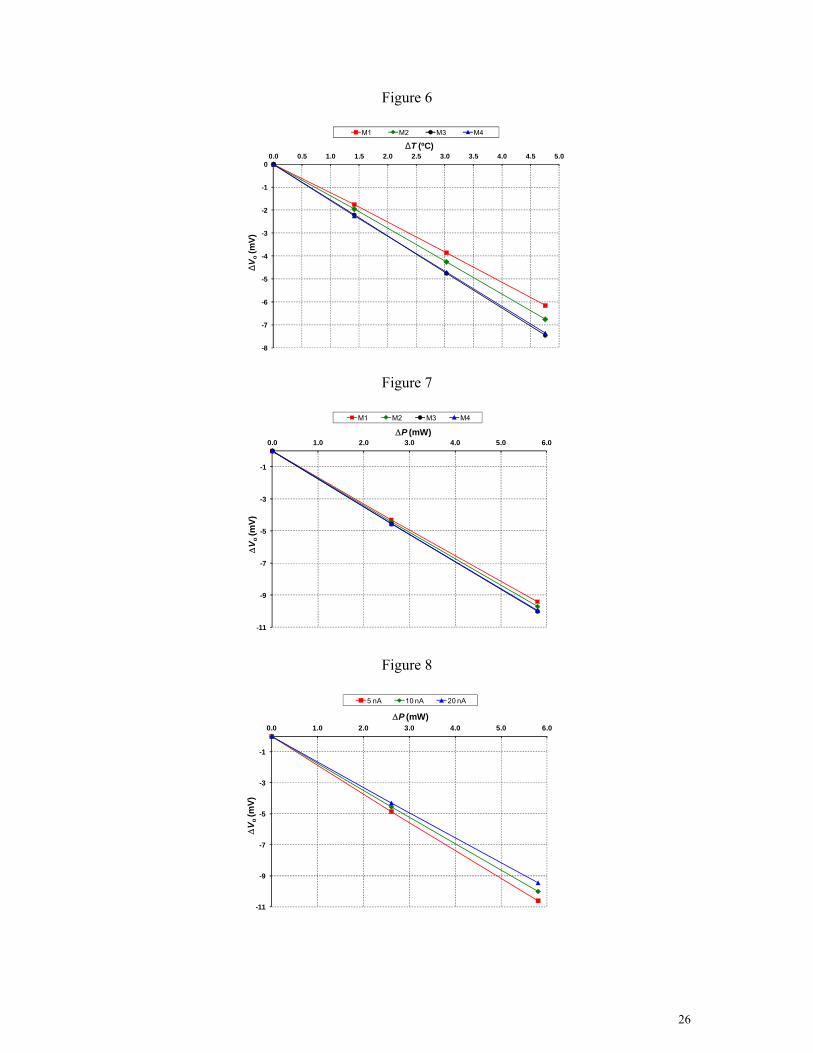
temperatures. The results are represented in Fig. 6, where the output voltage decreases
linearly with temperature and, in addition, the higher the factor W/L, the higher the sensitivity,
the same as in Fig. 2. If a straight line is fitted to the experimental data in Fig. 6 by means of
the least-square method, the resulting maximum nonlinearity error (expressed as a percentage
of the full-scale span, FSS) for the four MOSFETs is around 0.5 % FSS, which is an
acceptable value for IC testing purposes. The experimental values of ST resulting from Fig. 6
and the corresponding value normalized to the maximum are reported in Table II. Note that
the experimental values of ST are very similar to those resulting from simulations (differences
are smaller than 5 %). Experimental tests with the heating chamber also showed that the
voltage follower was not able to correctly read the sensor output voltage at high temperatures
(say, over 70 ºC) because the voltage was smaller than 200 mV.
The temperature sensors have been then tested at room temperature to monitor on-chip
thermal variations generated by the embedded heaters, as shown in Fig. 5d. The sensor was
biased and measured using the same instrumentation indicated in Fig. 5c, whereas the heater

13
was driven externally by a DC voltage source (Agilent E3631A); the current-voltage
characteristic of the heater was previously acquired using R6240A and, therefore, the current
(and, hence, the power) applied to the heater was accurately known for any voltage supplied
later by E3631A. Using this set-up, the steady-state output voltage of the sensors was
measured for different values of DC power applied to the heater and, then, SP was calculated.
The effects of the power dissipated by the heater on the sensor output voltage are
represented in Fig. 7 for different MOSFETs biased with IB = 10 nA, and in Fig. 8 for
different bias currents applied to M3. In both figures, the output voltage decreases linearly
with the dissipated power, as expected. Comparing the simulation results in Fig. 2 with the
experimental results in Fig. 7, we realize that in both cases the sensitivity increases with W/L,
but such an increase is smaller in Fig. 7. This discrepancy can also be observed by contrasting
the normalized values of SP resulting from Fig. 7 with those of ST resulting from Fig. 2, as
reported in Table II. Maybe the effective temperature change detected by the sensor was
smaller than that expected for MOSFETs with a high W (i.e. when the dimensions of the
sensor were comparable to those of the heater) and, for this reason, there are such differences
between Figs. 2 and 7. On the other hand, comparing the simulation results in Fig. 3 with the
experimental results in Fig. 8, we can see that the effects of bias current on ST and SP are very
similar. In both figures, the sensitivity increases with the same factor as the bias current
decreases.
The spread of SP due to process variations has also been experimentally evaluated by
testing nine samples of the designed chip from the same batch. For example, ΔSP/SP was
1.2 % for M3 using IB = 10 nA; ΔSP is assumed to be one standard deviation of SP, in such a
case: 20 µV/mW over 1.72 mV/mW. Such an experimental value of ΔSP/SP is slightly higher
than the simulated value of ΔST/ST presented in Section IV and, consequently, the limitations
of the Monte Carlo analysis indicated before do not seem so critical for a first estimation of

14
the spread. In comparison with the experimental results reported in [10], MOSFETs operating
in weak inversion offer values of ΔSP/SP very similar to those obtained with BJTs.
VI. DISCUSSION AND CONCLUSIONS
The work presented herein together with that in [10] enable us to compare the
performance of MOSFETs in weak inversion with that in strong inversion and also with that
of parasitic (vertical) BJTs, always in the context of on-chip thermal testing. As summarized
in Table III, several topics can be compared:
(a) CMOS compatibility: MOSFETs (either in strong or in weak inversion) are fully
CMOS compatible and, therefore, they are preferable for the on-chip thermal testing
of ICs fabricated in a CMOS process.
(b) Area: In CMOS technology, the use of parasitic BJTs is not as flexible as that of
MOSFETs in terms of area. The well-characterized parasitic BJTs available in the
design kits generally occupy a layout area that is much larger (say, ten times more)
than that required using MOSFETs (either in strong or in weak inversion); for
instance, the emitter area is 10 x 10 µm2 in 0.35 µm from AMS, 10 x 20 µm2 in [9],
and 15 x 15 µm2 in [25]. For the application described in Section II, a parasitic BJT
with a smaller emitter area could be valid, but no reliable simulations could be carried
out because of the lack of models; a preliminary tape-out intended for the
experimental characterization of those small parasitic BJTs could solve such a
limitation but at the expense of a higher cost. Note that this discussion about area
mainly focuses on that occupied by the sensing transistor (and not that of the bias
circuit or the BPF) since it is the most critical for the testing application of interest: the
sensing transistor must be small enough to fit within the empty areas of the layout of
the CUT with minimum impact on its design.

15
(c) Sign of ST: The output voltage of both MOSFETs in weak inversion and BJTs has a
negative temperature coefficient, whereas that of MOSFETs in strong inversion
usually shows a positive temperature coefficient.
(d) Magnitude of |ST|: Using the sensitivity to temperature of BJTs as a reference, the
sensitivity of MOSFETs in weak inversion is lower (around 20-30% lower), whereas
that in strong inversion can be significantly higher (more than three times higher).
(e) Advices to increase |ST|: The guidelines to increase the sensitivity to temperature in
weak inversion (i.e. high W/L and low bias current) are opposite to those obtained in
strong inversion (i.e. low W/L and high bias current). In terms of output noise voltage
and output resistance, it is preferable to increase |ST| by using a higher value of W/L in
weak inversion and a higher value of the bias current in strong inversion. The fact of
using a lower value of the bias current in weak inversion or a lower value of W/L in
strong inversion not only increases |ST|, but also the output noise voltage (to be
precise, the white noise component) and the output resistance and, therefore, the
circuit in Fig. 1b becomes more susceptible to interference and the loading effects of
the ensuing BPF (Fig. 1a) could be higher. As for the flicker noise component, the
higher the factor W·L, the smaller the output noise voltage [20], but the higher the area
required around the CUT.
(f) Spread of ST due to process variations: MOSFETs in weak inversion and BJTs have a
similar susceptibility to process variations (i.e. ΔST/ST ≈ 1%), which is around four
times better than that obtained with MOSFETs in strong inversion. Note, however,
that these results come from the experimental test of a reduced number of samples
from the same batch and, therefore, higher values of spread could be expected if
samples from different production batches were tested.

16
(g) Linearity: In the industrial temperature range, MOSFETs in weak inversion offer a
higher linearity (up to ten times more) and, therefore, the change of the output signal is
expected to be almost the same regardless of the operating temperature.
(h) Current consumption: The required bias current is in the range of nanoamperes for
MOSFETs in weak inversion, nanoamperes or microamperes for parasitic BJTs [9],
and microamperes for MOSFETs in strong inversion [10]. If the opamp needed for the
BPF in Fig. 1a has a current consumption of tens of microamperes, then the bias
current of the MOSFET sensor becomes negligible in weak inversion but not in strong
inversion and, consequently, the overall current consumption of the temperature
sensor circuit is expected to be higher in strong inversion; note that the current
consumption of the bias circuit is not assumed before because the temperature sensor
circuit could easily make a good use of the bias circuit of the CUT.
According to the previous discussion, the major benefits of using MOSFETs in weak
inversion in comparison with BJTs are: higher CMOS compatibility and lower layout area
around the CUT. On the other hand, in comparison with MOSFETs in strong inversion,
MOSFETs in weak inversion offer the following advantages: lower spread of ST due to
process variations (but always taking into account that the study here has been limited to a
reduced number of samples from the same batch) and lower current consumption; this is,
however, at the expense of a lower value of ST. The CUT to be tested applying the technique
explained in Section II will also play a significant role in the selection of the most appropriate
sensing transistor. For instance, for the on-chip thermal testing of a CUT that generates low
changes of temperature, a MOSFET in strong inversion seems more appropriate because it
offers higher values of ST. On the other hand, for a CUT that causes significant changes of
temperature, a MOSFET in weak inversion could be more attractive since it enables us to
optimize the testing sensor circuit in terms of power consumption.
For CMOS technologies different than that tested herein (i.e. 0.35 μm from AMS), we can

17
expect results similar to those shown in Table II provided that their technology parameters are
similar to those presented in Table I; this has been proved through simulations carried out in
0.18 μm CMOS technology from United Microelectronic Corporation (UMC). For
technologies whose parameters are not so similar to those in Table I, the numerical results in
Table II are not valid, but the qualitative conclusions given in Table III (for instance, advices
to increase the sensitivity) are applicable; this has been proved through simulations performed
in a 65 nm CMOS technology. Regardless of the technology being used, it is not
recommended to design a MOSFET temperature sensor with the smallest value of L or W, as
usually happens in analog IC design, since it could increase both the output noise voltage and
the spread of the sensitivity to temperature, as suggested by (11).
ACKNOWLEDGMENTS
This work has been funded by EU-Feder and Spanish MICINN under the TEC2008-01856
project and by AGAUR SGR 1497 funds. Authors highly appreciate the technical support of
Enrique Barajas in the design of the chip layout.

18
REFERENCES
[1] M. Sasaki, M. Ikeda, and K. Asada, “A temperature sensor with an inaccuracy of -1/+0.8
ºC using 90-nm 1-V CMOS for online thermal monitoring of VLSI circuits,” IEEE Trans.
Semicond. Manufacturing, vol. 21, no. 2, pp. 201-208, May 2008.
[2] P. Ituero, J.L. Ayala, and M. López-Vallejo, “A nanowatt smart temperature sensor for
dynamic thermal management,” IEEE Sensors Journal, vol. 8, no. 12, pp. 2036-2043,
Dec. 2008.
[3] J. Altet, D. Gomez, X. Perpinyà, D. Mateo, J.L. González, M. Vellvehí, and X. Jordà,
“Efficiency determination of RF linear power amplifiers by steady-state temperature
monitoring using built-in sensors,” Sens. Actuators A, Phys., vol. 192, pp. 49-57, 2013.
[4] E. Aldrete-Vidrio, D. Mateo, J. Altet, M. Amine Salhi, S. Grauby, S. Dilhaire, M.
Onabajo, and J. Silva-Martinez, “Strategies for built-in characterization testing and
performance monitoring of analog RF circuits with temperature measurements,” Meas.
Sci. Technol., vol. 21, pp. 075104 (10pp), 2010.
[5] Q. Yin, W.R. Eisenstadt, R.M. Fox, and T. Zhang, “A translinear RMS detector for
embedded test of RF ICs,” IEEE Trans. Instrum. Meas., vol. 54, no. 5, pp. 1708-1714,
Oct. 2005.
[6] A. Valdes-Garcia, R. Venkatasubramanian, J. Silva-Martinez, and E. Sánchez-Sinencio,
“A broadband CMOS amplitude detector for on-chip RF measurements,” IEEE Trans.
Instrum. Meas., vol. 57, no. 7, pp. 1470–1477, July 2008.
[7] C. Li, F. Gong, and P. Wang, “A low-power ultrawideband CMOS power detector with an
embedded amplifier,” IEEE Trans. Instrum. Meas., vol. 59, no. 12, pp. 3270–3278, Dec.
2010.
[8] F. Reverter, D. Gómez, and J. Altet, “On-chip MOSFET temperature sensor for electrical
characterization of RF circuits,” IEEE Sensors Journal, vol. 13, no. 9, pp. 3343-3344,
Sept. 2013.

19
[9] G. Wang and G.C.M. Meijer, “The temperature characteristics of bipolar transistors
fabricated in CMOS technology,” Sens. Actuators A, Phys., vol. 87, pp. 81-89, 2000.
[10] F. Reverter and J. Altet, “MOSFET temperature sensors for on-chip thermal testing,”
Sens. Actuators A, Phys., vol. 203, pp. 234-240, 2013.
[11] A. Kölling, F. Bak, P. Bergveld, and E. Seevinck, “Design of a CMOS temperature
sensor with current output,” Sens. Actuators, vol. A21-A23, pp. 645-649, 1990.
[12] K. Ueno, T. Asai, and Y. Amemiya, “Low-power temperature-to-frequency converter
consisting of subthreshold CMOS circuits for integrated smart temperature sensors,” Sens.
Actuators A, Phys., vol. 165, pp. 132-137, 2011.
[13] D. Gómez, C. Dufis, J. Altet, D. Mateo, and J. L. González, “Electro-thermal coupling
analysis methodology for RF circuits,” Microelectronics J., vol. 43, pp. 633-641, 2012.
[14] J. Kuntner, F. Kohl, and B. Jakoby, “Simultaneous thermal conductivity and
diffusivity sensing in liquids using a micromachined device,” Sens. Actuators A, Phys.,
vol. 130-131, pp. 62-67, 2006.
[15] D. F. Reyes-Romero, O. Behrmann, G. Dame, and G. A. Urban, “Dynamic thermal
sensor for biofilm monitoring,” Sens. Actuators A, Phys., vol. 213, pp. 43-51, 2014.
[16] A. Wang, B. Highsmith, and A.P. Chandrakasan, Sub-threshold Design for Ultra Low-
Power Systems, New York: Springer, 2006.
[17] E. Vittoz and J. Fellrath, “CMOS analog integrated circuits based on weak inversion
operation,” IEEE Journal of Solid-State Circuits, vol. 12, no. 3, pp. 224-231, June 1977.
[18] Y.P. Tsividis, Operation and Modelling of the MOS Transistor, New York: McGraw-
Hill, 1987.
[19] 0.35 µm CMOS C35 Process Parameters, AustriaMicroSystems, 2008.
[20] B. Razavi, Design of Analog CMOS Integrated Circuits, New York: McGraw-Hill,
2001.
[21] V. Székely, M. Rencz, S.Török, Cs. Márta, and L. Lipták-Fegó, “CMOS temperature

20
sensors and built-in test circuitry for thermal testing of ICs,” Sens. Actuators A, Phys., vol.
71, pp. 10-18, 1998.
[22] R. Sarpeshkar, Ultra Low Power Bioelectronics, New York: Cambridge University
Press, 2010.
[23] ISO 1993, Guide to the Expression of Uncertainty in Measurement, Geneva:
International Organization for Standardization, corrected and reprinted 1995.
[24] I.M. Filanovsky and A. Allam, “Mutual compensation of mobility and threshold
voltage temperature effects with applications in CMOS circuits,” IEEE Trans. Circuits
and Systems-I, vol. 48, no. 7, pp. 876-884, July 2001.
[25] M.A.P. Pertijs, G.C.M. Meijer, and J.H. Huijsing, “Precision temperature
measurement using CMOS substrate PNP transistors,” IEEE Sensors Journal, vol. 40, no.
3, pp. 294-300, June 2004.
21
SHORT BIOGRAPHIES
Ferran REVERTER was born in Llagostera, Spain, on January 4, 1976. He received the
B.Sc. degree in Industrial Electronic Engineering from the University of Girona (Girona,
Spain) in 1998, the M.Sc. degree in Electronic Engineering from the University of Barcelona
(Barcelona, Spain) in 2001, and the Ph.D. degree in Electronic Engineering from the
Universitat Politècnica de Catalunya (UPC) (Barcelona, Spain) in 2004. Since 2001 he has
been with the UPC, where he is an Associate Professor in Analogue Electronics and Digital
Systems. He was a visiting postdoctoral researcher with the Delft University of Technology
(Delft, The Netherlands) from 2005 to 2007, and with the Imperial College London (London,
UK) in 2012. He is coauthor of the book Direct sensor-to-microcontroller interface circuits
(Barcelona: Marcombo, 2005). His research interests are in the field of electronic
instrumentation, in particular, the design of interface circuits for smart sensors.
Josep ALTET received the Engineering degree from the La Universitat Ramon Llull, La
Salle and the Ph.D. degree from the Universitat Politècnica de Catalunya, UPC, Barcelona.
He completed postdoctoral stays at The University of British Columbia, Université Bordeaux
I, Centre Nacional de Microelectrònica, and Texas A&M University. He is currently in the
Department of Electronic Engineering, UPC, as Associate Professor. His research interests
include VLSI design and test, temperature sensor design, and thermal coupling analysis and
modeling in integrated circuits with applications to test and characterization of ICs.

22
List of Figure Captions
Figure 1. (a) Sensor circuit for the measurement of on-chip low-frequency temperature signals
resulting from the heterodyne technique. (b) Diode-connected MOSFET used as a
temperature sensor (T1) in Fig. 1a.
Figure 2. Simulated output-voltage change versus temperature for different MOSFETs biased
with IB = 10 nA.
Figure 3. Simulated output-voltage change of M3 versus temperature for different bias
currents.
Figure 4. Simulated relative change of ST versus the operating temperature for different
MOSFETs biased with IB = 10 nA.
Figure 5. (a) Sketch of the layout of the designed chip showing a heater-sensor pair. (b)
Schematic of the electronics embedded into the designed chip. (c) Set-up to test the response
of the sensors to temperature changes inside a heating camber. (d) Set-up to test the response
of the sensors to on-chip thermal variations caused by the power dissipated by the embedded
heater.
Figure 6. Experimental output voltage versus temperature for different MOSFETs biased with
IB = 10 nA. The horizontal axis represents the increase of temperature (ΔT) applied through
the heating chamber, whereas the vertical axis represents the change of voltage (ΔVo) with
respect to that obtained at ΔT = 0.
Figure 7. Experimental output voltage versus power for different MOSFETs biased with
IB = 10 nA. The horizontal axis represents the increase of power (ΔP) dissipated by the heater,
whereas the vertical axis represents the change of voltage (ΔVo) with respect to that obtained
at ΔP = 0.
Figure 8. Experimental output voltage of M3 versus power for different bias currents. The
horizontal axis represents the increase of power (ΔP) dissipated by the heater, whereas the

23
vertical axis represents the change of voltage (ΔVo) with respect to that obtained at ΔP = 0.
List of Table Captions
Table I. Main technology parameters for an n-type MOSFET in 0.35 µm CMOS technology
of AMS.
Table II. Theoretical, simulated and experimental values of sensitivity to temperature (ST),
and experimental values of sensitivity to power (SP) for different MOSFETs biased with
IB = 10 nA.
Table III. Comparative analysis between BJT- and MOSFET-based temperature sensors
operating in either strong or weak inversion.
24
Figure 1
f1
RF-CUT+
f2=f1+ f
T1
IC Isotherms at f
Amplif. BPF
(a) (b)
VDD
Vo
IB
W/LVGS
+
Vo
Figure 2
-7
-6
-5
-4
-3
-2
-1
00.0 0.5 1.0 1.5 2.0 2.5 3.0 3.5 4.0
ΔV o
(mV)
ΔT (ºC)M1 M2 M3 M4
Figure 3
-7
-6
-5
-4
-3
-2
-1
00.0 0.5 1.0 1.5 2.0 2.5 3.0 3.5 4.0
ΔV o
(mV)
ΔT (ºC)5 nA 10 nA 20 nA

25
Figure 4
0.0
0.5
1.0
1.5
2.0
2.5
-40 -20 0 20 40 60 80
Rel
ativ
e ch
ange
of S
T(%
)
T (ºC)
M1 M2 M3 M4
Figure 5
Iext
R6240AE3631A
Chip
30
m
30 m
Lh=1 m
L
WHeater
5 m
(a)
(d)
HP 3458A
Pt10
0
4W
Heating chamber
sens
or
Sensor
Chip
Current mirror
W/L
Vo
(b)
IBPin
Heater
Isotherms
Iext
Pin
V
Vo
HP34401A
Iext
R6240A
Chip
(c)
V
Vo
HP34401A
26
Figure 6
-8
-7
-6
-5
-4
-3
-2
-1
00.0 0.5 1.0 1.5 2.0 2.5 3.0 3.5 4.0 4.5 5.0
ΔVo
(mV)
ΔT (ºC)M1 M2 M3 M4
Figure 7
-11
-9
-7
-5
-3
-1
0.0 1.0 2.0 3.0 4.0 5.0 6.0
ΔV o
(mV)
ΔP (mW)M1 M2 M3 M4
Figure 8
-11
-9
-7
-5
-3
-1
0.0 1.0 2.0 3.0 4.0 5.0 6.0
ΔV o
(mV)
ΔP (mW)
5 nA 10 nA 20 nA

27
Table I
Parameter Value µ0 370 cm2/V/s
VTH0 0.4979 V α −1.8 β −1.1 mV/K
tOX 7.6 nm
Table II
Sensor W (µm)
L (µm)
Theoretical results Simulation results
Experimental results
Heating chamber Power applied to the heater
ST (mV/K)
ST (mV/K)
Norm. ST
ST (mV/K)
Norm. ST
SP (mV/mW)
Norm. SP
M1 1 1 -1.32 -1.22 0.80 -1.29 0.82 -1.62 0.94 M2 4 1 -1.50 -1.38 0.90 -1.42 0.90 -1.67 0.97 M3 16 1 -1.68 -1.53 1 -1.57 1 -1.72 1 M4 24 1.5 -1.68 -1.53 1 -1.54 0.98 -1.72 1
Table III
BJT MOSFET in strong inversion
MOSFET in weak inversion
CMOS compatibility Low-Medium High High Area High Low Low
Sign of ST Negative Positive Negative Magnitude of |ST| Medium Medium-High Low-Medium
Advices to increase |ST| -- (W/L) ↓ and IB ↑ (W/L) ↑ and IB ↓ Spread of ST due to process Low Medium Low
Linearity in [-40,85]ºC Medium-High Medium-High High Current consumption Low-Medium Medium Low