Embed Size (px)
Citation preview
Portland State University Portland State University
PDXScholar PDXScholar
University Honors Theses University Honors College
8-17-2017
On Finding a Simulation Model for Carbon On Finding a Simulation Model for Carbon
Nanotubes as Through-Silicon-Vias Nanotubes as Through-Silicon-Vias
Alec Wiese Portland State University
Follow this and additional works at: https://pdxscholar.library.pdx.edu/honorstheses
Let us know how access to this document benefits you.
Recommended Citation Recommended Citation Wiese, Alec, "On Finding a Simulation Model for Carbon Nanotubes as Through-Silicon-Vias" (2017). University Honors Theses. Paper 471. https://doi.org/10.15760/honors.471
This Thesis is brought to you for free and open access. It has been accepted for inclusion in University Honors Theses by an authorized administrator of PDXScholar. Please contact us if we can make this document more accessible: [email protected].
On Finding a Simulation Model for Carbon Nanotubes as
Through-Silicon-Vias
by
Alec Wiese
An undergraduate honors thesis submitted in partial fulfillment of the
requirements for the degree of
Bachelor of Science
in
University Honors
and
Electrical Engineering
Thesis Adviser
Dr. James Morris
Portland State University
2017
1. Abstract:
This paper outlines the electrical and thermal properties of carbon nanotubes (CNT) as a
potential replacement for Copper (Cu) in through silicon vias (TSV). Cu has undesirable thermal
properties, and CNTs could resolve issues that high density interconnects experience under high
thermal loads around 100 C. Most notably, the coefficient of thermal expansion for CNTs is two
orders of magnitude lesser than Cu [1]. The electrical and mechanical properties of CNTs under
a high frequency load of 1 THz, and high thermal load of 100 C are simulated with ABAQUS
6.16. There is no observable skin effect modelled for the Cu or Single-Walled Carbon Nanotube
(SWCNT) wires simulated in this paper.
2. Introduction:
Digital ICs (integrated circuits) are very common in electronics, as well as solid state
drives (i.e. flash memory), and the ever-increasing demand for faster, cheaper, and more dense
electronics drives for more innovative solutions. Transistors, as the building blocks of
electronics, follow Moore’s law and become 2X smaller and smaller approximately every two
years, which allows electronics to continue to decrease in the surface area they take up. To
reduce interconnect length and increase speed, a rather practical solution is to stack chips on
top of each other. This allows us to use the third dimension, and interconnect devices with
Through Silicon Vias (TSV) and allow for high speed/low latency connections while avoiding
extra PCB costs. When chips are stacked on top of each other, the usual materials in vias, like
copper, expand and contract due to thermal stress. This is due to thermal stress and the
Coefficient of Thermal Expansion (CTE) for different materials [1]. A larger CTE means that a
material has a higher tendency to expand due to an increase in temperature. Copper has a very
high conductivity and is the most common conductor used in electronics [2] due to its low cost.
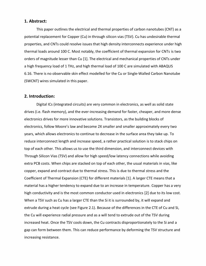
When a TSV such as Cu has a larger CTE than the Si it is surrounded by, it will expand and
extrude during a heat cycle (see Figure 2.1). Because of the differences in the CTE of Cu and Si,
the Cu will experience radial pressure and as a will tend to extrude out of the TSV during
increased heat. Once the TSV cools down, the Cu contracts disproportionately to the Si and a
gap can form between them. This can reduce performance by deforming the TSV structure and
increasing resistance.
Figure 2.1 Demonstration of the behavior of Cu as a TSV under a thermal load
(Created with ANSYS AIM 18.1 Student Edition)
A solution to this is to use carbon nanotubes (CNT) or CNT-Metal composite TSVs that
can result in very similar CTE to that of silicon, mitigating the effects seen with Cu [2]. CNTs also
resolve some of the other issues with Cu such as electromigration [2]. Over time,
electromigration can cause reliability issues and disconnect Cu TSVs due to the movement of Cu
atoms. Therefore, it is of great interest to investigate how to take advantage of CNT or CNT
composite TSVs. This encourages us to use some other material with better thermal properties,
however we need to use something conductive to carry our signal. In a bundle, SWCNTs are
statistically 1/3 metallic and 2/3 semiconducting so we must assume an average resistivity for a
bundle [3]. CNTs have great thermal properties, such as a very low coefficient of thermal
expansion [3].
One interesting note is that for interconnects on the nanometer scale, CNTs can provide
the possibility for ballistic transport, where the mean free path of an electron is greater than
the length of a via. The mean free path of an electron in a Single-Walled Carbon Nanotube is
determined by:
𝑙𝑚𝑓𝑝 = 𝐷[𝑘1 + 𝑘2𝑇 + 𝑘3𝑇2]−1 [4]
Where D is the diameter of the CNT and 𝑘1 = 3.01 ∙ 10−3, 𝑘2 = −2.12 ∙ 10−5𝐾−1, 𝑘3 = 4.7 ∙
10−8𝐾−2. For a diameter of 4nm we see mean free paths of 5.52 µm at 273 K (~0 C) and 2.44
µm at 373 K (~100 C).
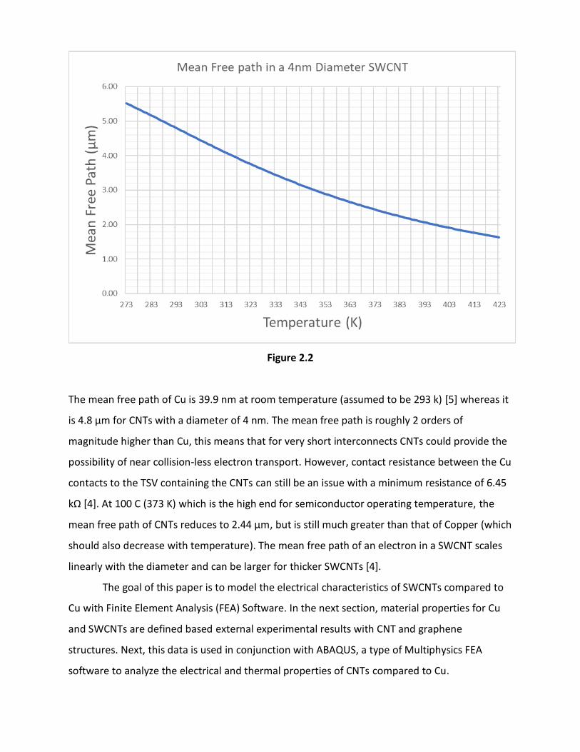
Figure 2.2
The mean free path of Cu is 39.9 nm at room temperature (assumed to be 293 k) [5] whereas it
is 4.8 µm for CNTs with a diameter of 4 nm. The mean free path is roughly 2 orders of
magnitude higher than Cu, this means that for very short interconnects CNTs could provide the
possibility of near collision-less electron transport. However, contact resistance between the Cu
contacts to the TSV containing the CNTs can still be an issue with a minimum resistance of 6.45
kΩ [4]. At 100 C (373 K) which is the high end for semiconductor operating temperature, the
mean free path of CNTs reduces to 2.44 µm, but is still much greater than that of Copper (which
should also decrease with temperature). The mean free path of an electron in a SWCNT scales
linearly with the diameter and can be larger for thicker SWCNTs [4].
The goal of this paper is to model the electrical characteristics of SWCNTs compared to
Cu with Finite Element Analysis (FEA) Software. In the next section, material properties for Cu
and SWCNTs are defined based external experimental results with CNT and graphene
structures. Next, this data is used in conjunction with ABAQUS, a type of Multiphysics FEA
software to analyze the electrical and thermal properties of CNTs compared to Cu.
3. Model Setup:
SWCNT bundles can be fabricated with a maximum aspect ratio of about 300:1 at
several hundred micrometers tall, with a bundle diameter of 200 µm [2]. Since wafers are
typically 20-150 µm thick, we are well within the range of growth for CNTs. Model 1 and Model
2 have been designed with 0.1 µm length to achieve the finest mesh possible. A length this
short should result in ballistic conduction, as 0.1 µm is much shorter than the 𝑙𝑚𝑓𝑝 of 2.44 µm
at 373 K. However, since ABAQUS will not consider ballistic conduction, the length is sufficient
to show electrical effects for a longer via.
Commonly accepted values were used for Cu for material properties outlined in Table
3.1. A range of sources was required to get material property values for CNTs, which are
specified in Table 3.2 and Table 3.3. Table 3.2 shows the macroscopic properties of CNT
bundles, whereas Table 3.3 shows the properties adjusted for a SWCNT with a diameter of 4
nm and a thickness of 0.335 nm [6]. This adjustment was done by changing values dependent
on volume and surface area. Since the SWCNT properties in Table 3.2 are macroscopic (for
bundles) and our ABAQUS model of a SWCNT is hollow, the material properties must be
adjusted such that this loss of surface area and volume is accounted for. With a thickness of
0.35 (0.335 nm from [6] rounded to nearest possible value with ABAQUS), the surface area is
4.013 nm-2 from equation (1). This adjusted surface area is 31.94% that of a solid wire with the
same diameter of 4 nm, so the properties depending on area and volume were multiplied by
the reciprocal of 0.3194 (3.131) to account for the hollow shape. E.g. Electrical Conductivity
increased from 2.9 S/µm to 9.08 S/µm (otherwise the hollow shape would have incorrectly
increased resistance for a SWCNT in our model).
𝑆𝑢𝑟𝑓𝑎𝑐𝑒 𝑎𝑟𝑒𝑎 𝑜𝑓 4 𝑛𝑚 𝑑𝑖𝑎𝑚𝑒𝑡𝑒𝑟 𝐶𝑁𝑇 = [𝜋 ∙ 22] − [𝜋 ∙ (2 − 0.35)2] 𝑛𝑚−2 (1)
SI units of time in seconds s were used, however length and mass units were converted
from SI and are based on µg, µm rather than Kg and m respectively. This is due to the accuracy
handling of ABAQUS. Units were converted because using SI units in ABAQUS resulted in many
output values being rounded to zero.
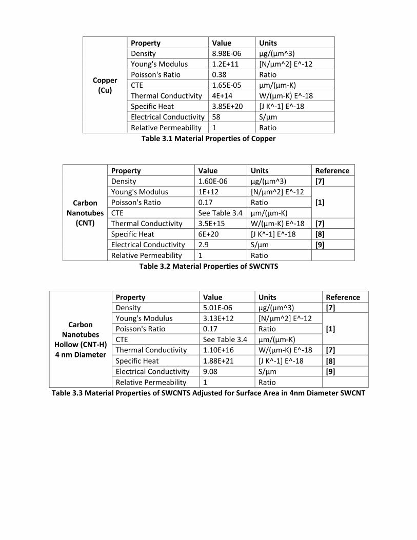
Copper (Cu)
Property Value Units
Density 8.98E-06 µg/(µm^3)
Young's Modulus 1.2E+11 [N/µm^2] E^-12
Poisson's Ratio 0.38 Ratio
CTE 1.65E-05 µm/(µm-K)
Thermal Conductivity 4E+14 W/(µm-K) E^-18
Specific Heat 3.85E+20 [J K^-1] E^-18
Electrical Conductivity 58 S/µm
Relative Permeability 1 Ratio
Table 3.1 Material Properties of Copper
Carbon Nanotubes
(CNT)
Property Value Units Reference
Density 1.60E-06 µg/(µm^3) [7]
Young's Modulus 1E+12 [N/µm^2] E^-12
[1] Poisson's Ratio 0.17 Ratio
CTE See Table 3.4 µm/(µm-K)
Thermal Conductivity 3.5E+15 W/(µm-K) E^-18 [7]
Specific Heat 6E+20 [J K^-1] E^-18 [8]
Electrical Conductivity 2.9 S/µm [9]
Relative Permeability 1 Ratio
Table 3.2 Material Properties of SWCNTS
Carbon Nanotubes
Hollow (CNT-H) 4 nm Diameter
Property Value Units Reference
Density 5.01E-06 µg/(µm^3) [7]
Young's Modulus 3.13E+12 [N/µm^2] E^-12
[1] Poisson's Ratio 0.17 Ratio
CTE See Table 3.4 µm/(µm-K)
Thermal Conductivity 1.10E+16 W/(µm-K) E^-18 [7]
Specific Heat 1.88E+21 [J K^-1] E^-18 [8]
Electrical Conductivity 9.08 S/µm [9]
Relative Permeability 1 Ratio
Table 3.3 Material Properties of SWCNTS Adjusted for Surface Area in 4nm Diameter SWCNT
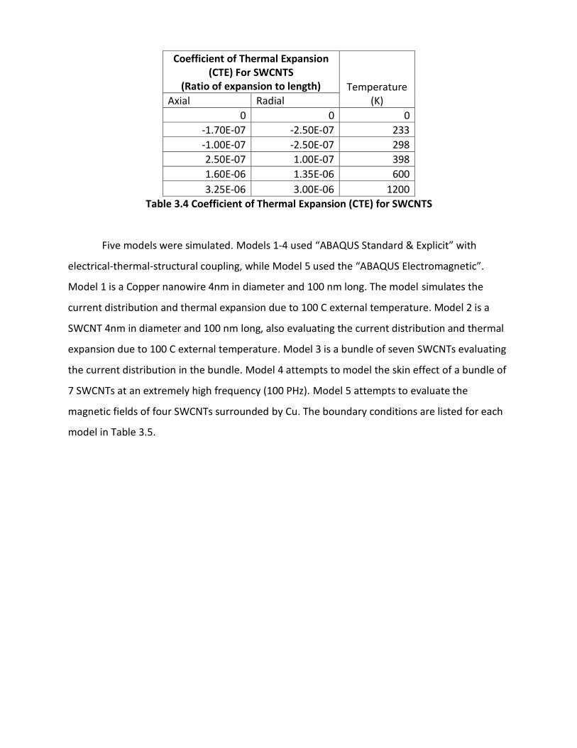
Coefficient of Thermal Expansion (CTE) For SWCNTS
(Ratio of expansion to length) Temperature (K) Axial Radial
0 0 0
-1.70E-07 -2.50E-07 233
-1.00E-07 -2.50E-07 298
2.50E-07 1.00E-07 398
1.60E-06 1.35E-06 600
3.25E-06 3.00E-06 1200
Table 3.4 Coefficient of Thermal Expansion (CTE) for SWCNTS
Five models were simulated. Models 1-4 used “ABAQUS Standard & Explicit” with
electrical-thermal-structural coupling, while Model 5 used the “ABAQUS Electromagnetic”.
Model 1 is a Copper nanowire 4nm in diameter and 100 nm long. The model simulates the
current distribution and thermal expansion due to 100 C external temperature. Model 2 is a
SWCNT 4nm in diameter and 100 nm long, also evaluating the current distribution and thermal
expansion due to 100 C external temperature. Model 3 is a bundle of seven SWCNTs evaluating
the current distribution in the bundle. Model 4 attempts to model the skin effect of a bundle of
7 SWCNTs at an extremely high frequency (100 PHz). Model 5 attempts to evaluate the
magnetic fields of four SWCNTs surrounded by Cu. The boundary conditions are listed for each
model in Table 3.5.
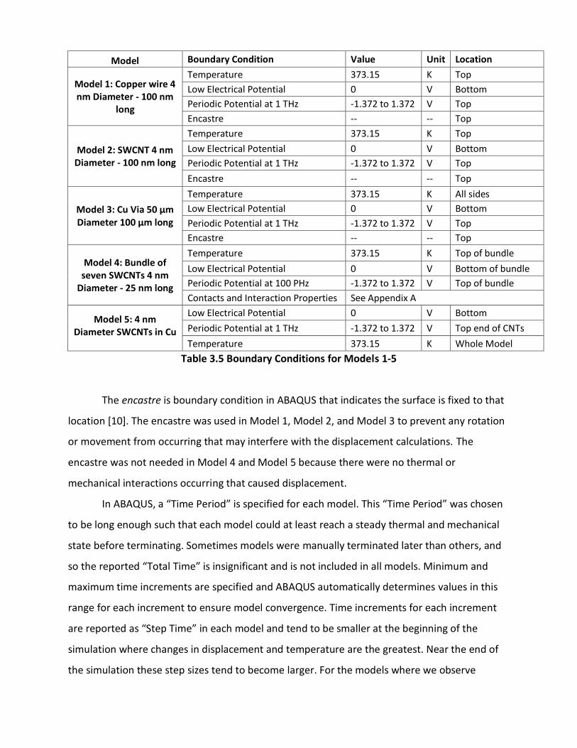
Model Boundary Condition Value Unit Location
Model 1: Copper wire 4 nm Diameter - 100 nm
long
Temperature 373.15 K Top
Low Electrical Potential 0 V Bottom
Periodic Potential at 1 THz -1.372 to 1.372 V Top
Encastre -- -- Top
Model 2: SWCNT 4 nm Diameter - 100 nm long
Temperature 373.15 K Top
Low Electrical Potential 0 V Bottom
Periodic Potential at 1 THz -1.372 to 1.372 V Top
Encastre -- -- Top
Model 3: Cu Via 50 µm Diameter 100 µm long
Temperature 373.15 K All sides
Low Electrical Potential 0 V Bottom
Periodic Potential at 1 THz -1.372 to 1.372 V Top
Encastre -- -- Top
Model 4: Bundle of seven SWCNTs 4 nm
Diameter - 25 nm long
Temperature 373.15 K Top of bundle
Low Electrical Potential 0 V Bottom of bundle
Periodic Potential at 100 PHz -1.372 to 1.372 V Top of bundle
Contacts and Interaction Properties See Appendix A
Model 5: 4 nm Diameter SWCNTs in Cu
Low Electrical Potential 0 V Bottom
Periodic Potential at 1 THz -1.372 to 1.372 V Top end of CNTs
Temperature 373.15 K Whole Model
Table 3.5 Boundary Conditions for Models 1-5
The encastre is boundary condition in ABAQUS that indicates the surface is fixed to that
location [10]. The encastre was used in Model 1, Model 2, and Model 3 to prevent any rotation
or movement from occurring that may interfere with the displacement calculations. The
encastre was not needed in Model 4 and Model 5 because there were no thermal or
mechanical interactions occurring that caused displacement.
In ABAQUS, a “Time Period” is specified for each model. This “Time Period” was chosen
to be long enough such that each model could at least reach a steady thermal and mechanical
state before terminating. Sometimes models were manually terminated later than others, and
so the reported “Total Time” is insignificant and is not included in all models. Minimum and
maximum time increments are specified and ABAQUS automatically determines values in this
range for each increment to ensure model convergence. Time increments for each increment
are reported as “Step Time” in each model and tend to be smaller at the beginning of the
simulation where changes in displacement and temperature are the greatest. Near the end of
the simulation these step sizes tend to become larger. For the models where we observe
displacement and temperature, at least two increments were observed where the maximum
displacement and temperature had not changed, and the final increment was reported. The
“Step Time” is also insignificant for these models. The “Time Period” and “Step Time” appear in
Models 1-4.
The “Time-Harmonic” frequency for the electromagnetic model is set in Model 5 as a
range from 0 to 1 THz (input as rad/s). This is in place of the “Time Period” from Models 1-4.
The total time is equivalent to the frequency value in each increment in ABAQUS
Electromagnetic models. It is unclear if the Frequency value has any effect.
The “Deformation Scale Factor” given in the model figures is set by ABAQUS and is the
ratio to 1 in which the deformation of the model is shown [11]. This is to aid visualization of
displacement deformation by exaggerating (when “Deformation Scale Factor” is greater than 1)
the deformation extent. This has no effect on the results, only the shape of the model in the
viewer. The Deformation Scale Factor is displayed in each model screenshot in Section 4. Since
the desired information is the absolute displacement, the “Deformation Scale Factor” is also
insignificant for our model, except as a visual aid.
4. Results:
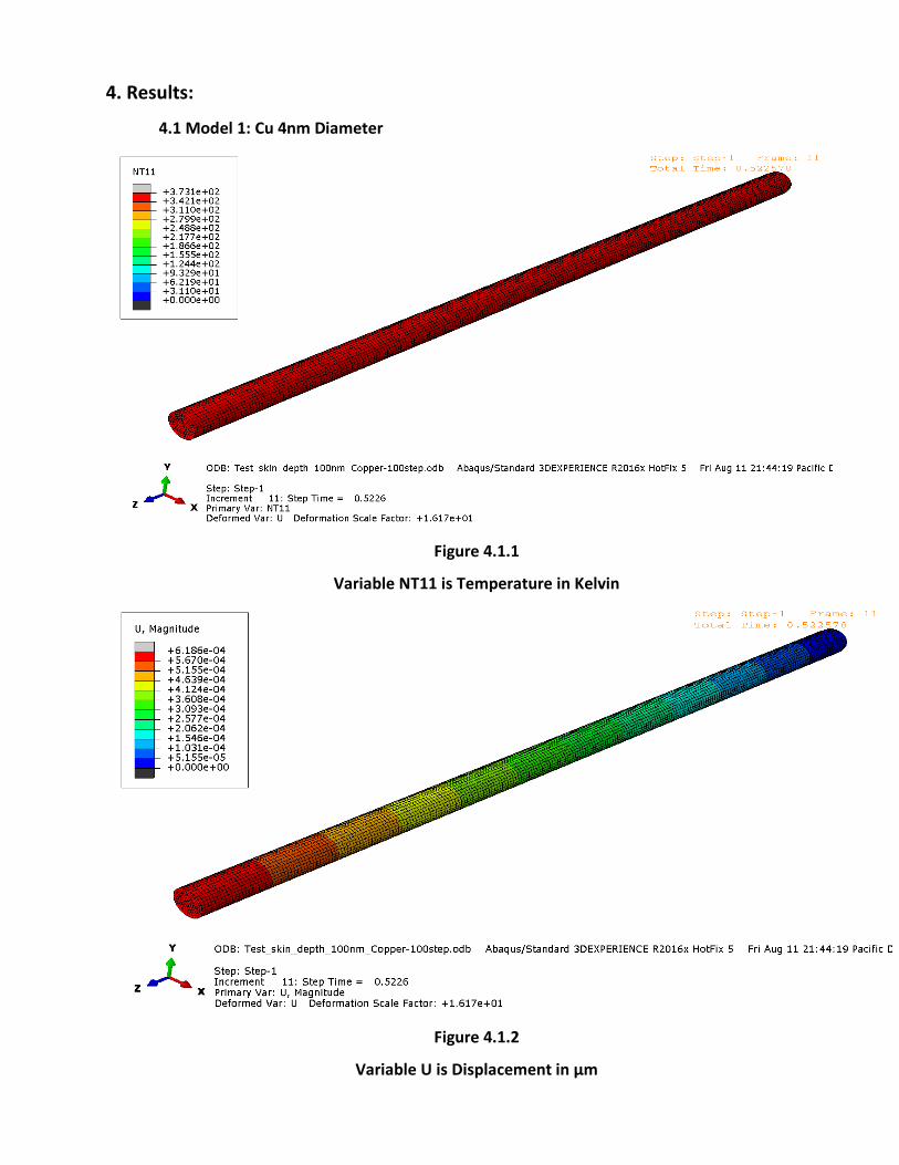
4.1 Model 1: Cu 4nm Diameter
Figure 4.1.1
Variable NT11 is Temperature in Kelvin
Figure 4.1.2
Variable U is Displacement in µm
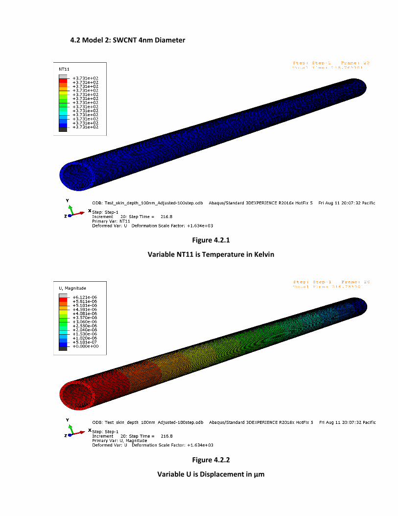
4.2 Model 2: SWCNT 4nm Diameter
Figure 4.2.1
Variable NT11 is Temperature in Kelvin
Figure 4.2.2
Variable U is Displacement in µm
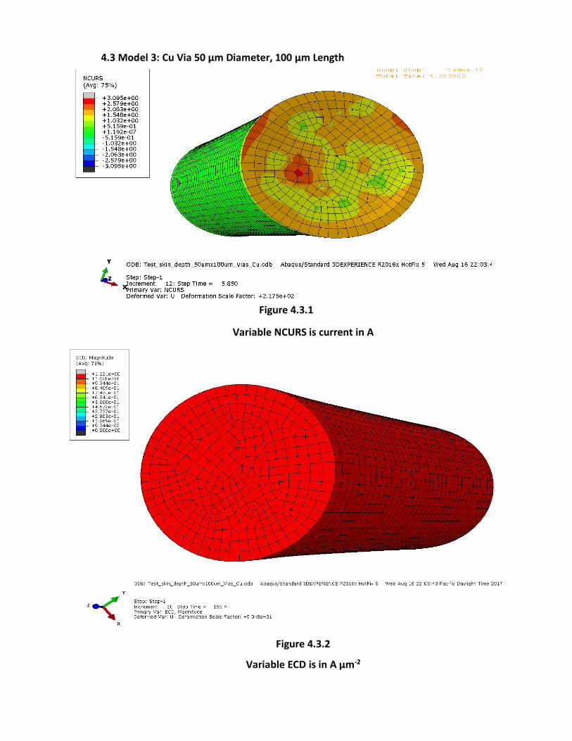
4.3 Model 3: Cu Via 50 µm Diameter, 100 µm Length
Figure 4.3.1
Variable NCURS is current in A
Figure 4.3.2
Variable ECD is in A µm-2
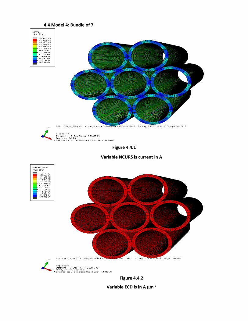
4.4 Model 4: Bundle of 7
Figure 4.4.1
Variable NCURS is current in A
Figure 4.4.2
Variable ECD is in A µm-2
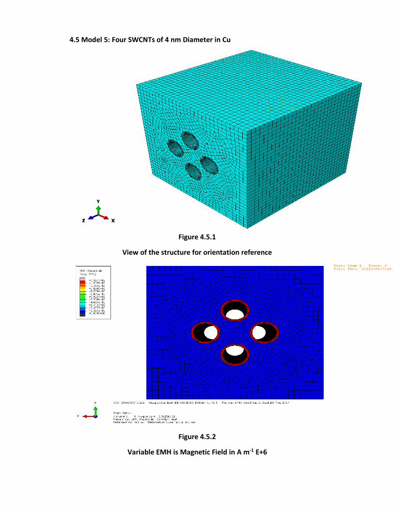
4.5 Model 5: Four SWCNTs of 4 nm Diameter in Cu
Figure 4.5.1
View of the structure for orientation reference
Figure 4.5.2
Variable EMH is Magnetic Field in A m-1 E+6
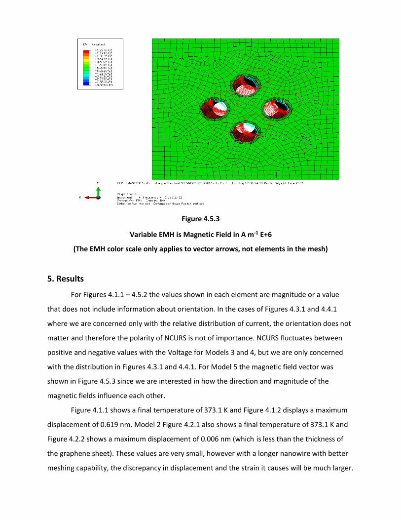
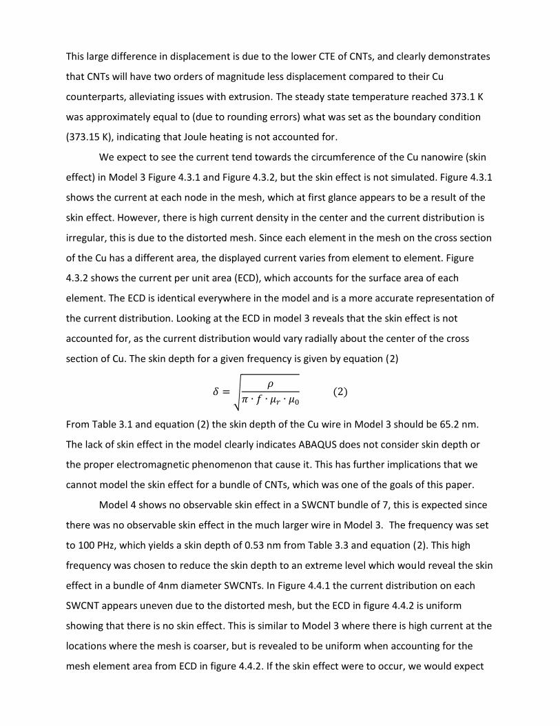
Figure 4.5.3
Variable EMH is Magnetic Field in A m-1 E+6
(The EMH color scale only applies to vector arrows, not elements in the mesh)
5. Results
For Figures 4.1.1 – 4.5.2 the values shown in each element are magnitude or a value
that does not include information about orientation. In the cases of Figures 4.3.1 and 4.4.1
where we are concerned only with the relative distribution of current, the orientation does not
matter and therefore the polarity of NCURS is not of importance. NCURS fluctuates between
positive and negative values with the Voltage for Models 3 and 4, but we are only concerned
with the distribution in Figures 4.3.1 and 4.4.1. For Model 5 the magnetic field vector was
shown in Figure 4.5.3 since we are interested in how the direction and magnitude of the
magnetic fields influence each other.
Figure 4.1.1 shows a final temperature of 373.1 K and Figure 4.1.2 displays a maximum
displacement of 0.619 nm. Model 2 Figure 4.2.1 also shows a final temperature of 373.1 K and
Figure 4.2.2 shows a maximum displacement of 0.006 nm (which is less than the thickness of
the graphene sheet). These values are very small, however with a longer nanowire with better
meshing capability, the discrepancy in displacement and the strain it causes will be much larger.
This large difference in displacement is due to the lower CTE of CNTs, and clearly demonstrates
that CNTs will have two orders of magnitude less displacement compared to their Cu
counterparts, alleviating issues with extrusion. The steady state temperature reached 373.1 K
was approximately equal to (due to rounding errors) what was set as the boundary condition
(373.15 K), indicating that Joule heating is not accounted for.
We expect to see the current tend towards the circumference of the Cu nanowire (skin
effect) in Model 3 Figure 4.3.1 and Figure 4.3.2, but the skin effect is not simulated. Figure 4.3.1
shows the current at each node in the mesh, which at first glance appears to be a result of the
skin effect. However, there is high current density in the center and the current distribution is
irregular, this is due to the distorted mesh. Since each element in the mesh on the cross section
of the Cu has a different area, the displayed current varies from element to element. Figure
4.3.2 shows the current per unit area (ECD), which accounts for the surface area of each
element. The ECD is identical everywhere in the model and is a more accurate representation of
the current distribution. Looking at the ECD in model 3 reveals that the skin effect is not
accounted for, as the current distribution would vary radially about the center of the cross
section of Cu. The skin depth for a given frequency is given by equation (2)
𝛿 = √𝜌
𝜋 ∙ 𝑓 ∙ 𝜇𝑟 ∙ 𝜇0 (2)
From Table 3.1 and equation (2) the skin depth of the Cu wire in Model 3 should be 65.2 nm.
The lack of skin effect in the model clearly indicates ABAQUS does not consider skin depth or
the proper electromagnetic phenomenon that cause it. This has further implications that we
cannot model the skin effect for a bundle of CNTs, which was one of the goals of this paper.
Model 4 shows no observable skin effect in a SWCNT bundle of 7, this is expected since
there was no observable skin effect in the much larger wire in Model 3. The frequency was set
to 100 PHz, which yields a skin depth of 0.53 nm from Table 3.3 and equation (2). This high
frequency was chosen to reduce the skin depth to an extreme level which would reveal the skin
effect in a bundle of 4nm diameter SWCNTs. In Figure 4.4.1 the current distribution on each
SWCNT appears uneven due to the distorted mesh, but the ECD in figure 4.4.2 is uniform
showing that there is no skin effect. This is similar to Model 3 where there is high current at the
locations where the mesh is coarser, but is revealed to be uniform when accounting for the
mesh element area from ECD in figure 4.4.2. If the skin effect were to occur, we would expect
Model 4 to show a lower concentration of current in the center SWCNT. Y. Feng and S. L.
Burkett calculate that the skin effect in a 1 µm diameter TSV of comprised of 4 nm diameter
SWCNTs is expected to be very limited [12]. As the diameter of the SWCNTs increase, the
calculated current density normalizes across the via, and the skin depth increases [12]. This
contrasts with E. K. Farahani and R. Sarvari where they calculate and model a more apparent
skin effect and skin depth in a 3 µm bundle of Multi-Walled Carbon Nanotubes (MWCNT) in the
100 GHz range [13]. The MWCNT bundles in [13] seem to be more subject to the skin effect
than the SWCNT bundles in [12], however this could be due to the 3 µm via diameter in [13]
compared to the 1 µm via diameter in [12] or differences in methodology.
Model 5 attempted to show that the magnetic fields due to AC current flow in CNTs
should interact with each other and affect the current flow of other CNTs. However, ABAQUS
does not allow for interactions in magnetic models and the resultant magnetic field vectors
were independent to each CNT. Figure 4.5.1 shows the 3-D structure of the model mesh, with 4
4nm diameter SWCNTs surrounded by Cu. Figure 4.5.2 shows that a positive magnetic field
exists in the SWCNTs, but the magnitude of the magnetic field is zero everywhere in the Cu
structure. This indicates that there are no electromagnetic interactions between structures in
ABAQUS. Figure 4.5.3 shows the magnetic field vectors (as opposed to just the magnitude from
Figure 4.5.2) which are identical in each SWCNT, and entirely absent in the Cu. In Figure 4.5.3
there is also no indication of electromagnetic interaction in the model.
6. Conclusions:
Models 1-5 indicate that ABAQUS is not ideal for modelling electromagnetic properties
of CNTs. Skin effect is not simulated, and interactions do not occur between structures in the
electromagnetic model. ABAQUS also does not consider ballistic transport or quantum effects
such as kinetic inductance, which could affect the results. ABAQUS was designed for
macroscopic mechanical modelling, and quantum effects are not calculated. While ABAQUS is
not well suited for electromagnetic analyses, it is designed for use in thermal and mechanical
analyses and could be helpful in determining the maximum temperature the CNT-Cu composite
can handle before the difference in CTE causes adhesive failure. External temperature would be
the main factor for mechanical failure since Joule heating is not accounted for.
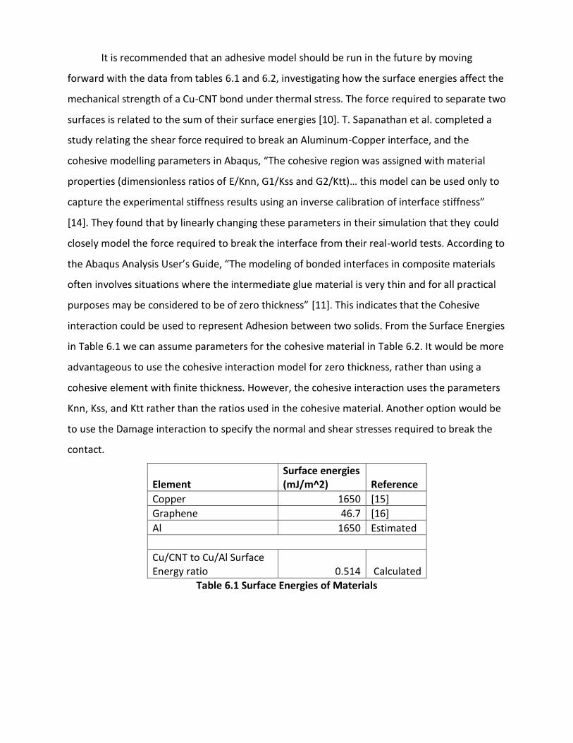
It is recommended that an adhesive model should be run in the future by moving
forward with the data from tables 6.1 and 6.2, investigating how the surface energies affect the
mechanical strength of a Cu-CNT bond under thermal stress. The force required to separate two
surfaces is related to the sum of their surface energies [10]. T. Sapanathan et al. completed a
study relating the shear force required to break an Aluminum-Copper interface, and the
cohesive modelling parameters in Abaqus, “The cohesive region was assigned with material
properties (dimensionless ratios of E/Knn, G1/Kss and G2/Ktt)… this model can be used only to
capture the experimental stiffness results using an inverse calibration of interface stiffness”
[14]. They found that by linearly changing these parameters in their simulation that they could
closely model the force required to break the interface from their real-world tests. According to
the Abaqus Analysis User’s Guide, “The modeling of bonded interfaces in composite materials
often involves situations where the intermediate glue material is very thin and for all practical
purposes may be considered to be of zero thickness” [11]. This indicates that the Cohesive
interaction could be used to represent Adhesion between two solids. From the Surface Energies
in Table 6.1 we can assume parameters for the cohesive material in Table 6.2. It would be more
advantageous to use the cohesive interaction model for zero thickness, rather than using a
cohesive element with finite thickness. However, the cohesive interaction uses the parameters
Knn, Kss, and Ktt rather than the ratios used in the cohesive material. Another option would be
to use the Damage interaction to specify the normal and shear stresses required to break the
contact.
Element Surface energies (mJ/m^2) Reference
Copper 1650 [15]
Graphene 46.7 [16]
Al 1650 Estimated
Cu/CNT to Cu/Al Surface Energy ratio 0.514 Calculated
Table 6.1 Surface Energies of Materials
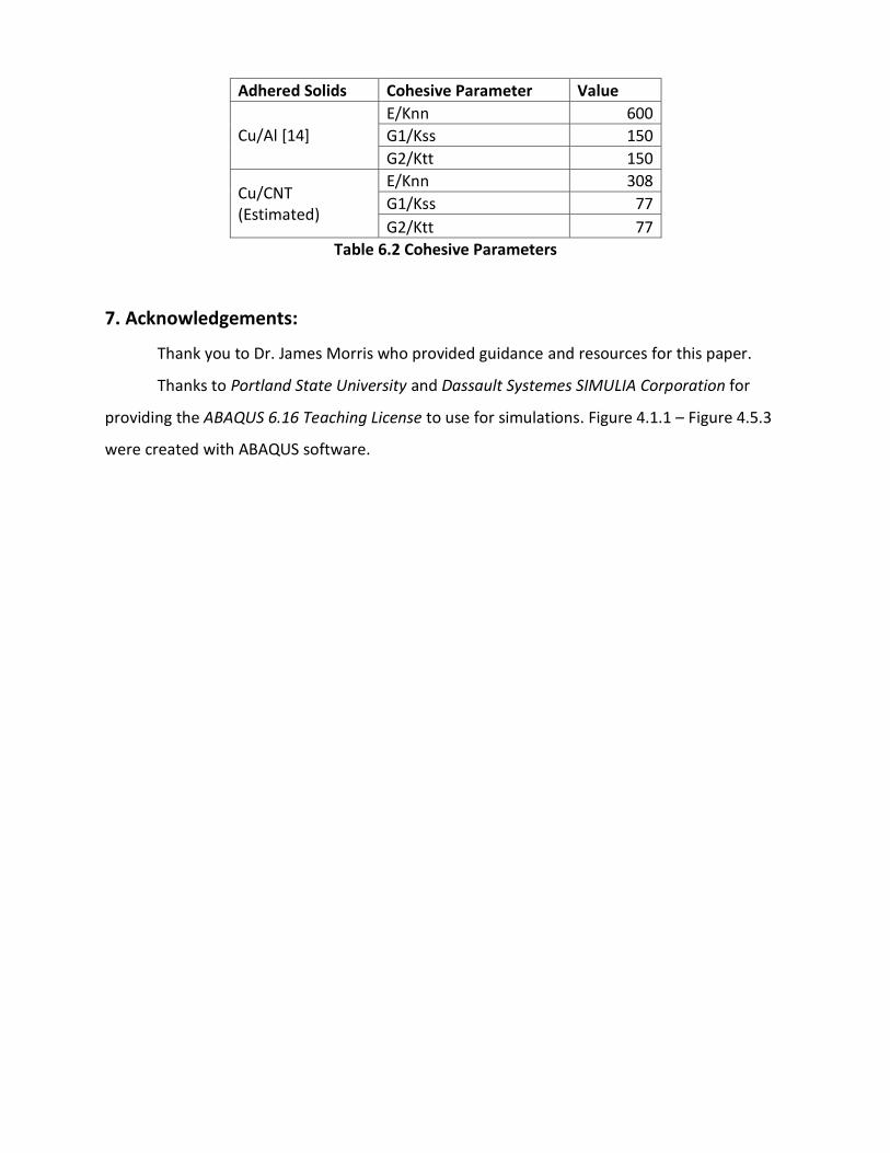
Adhered Solids Cohesive Parameter Value
Cu/Al [14]
E/Knn 600
G1/Kss 150
G2/Ktt 150
Cu/CNT (Estimated)
E/Knn 308
G1/Kss 77
G2/Ktt 77
Table 6.2 Cohesive Parameters
7. Acknowledgements:
Thank you to Dr. James Morris who provided guidance and resources for this paper.
Thanks to Portland State University and Dassault Systemes SIMULIA Corporation for
providing the ABAQUS 6.16 Teaching License to use for simulations. Figure 4.1.1 – Figure 4.5.3
were created with ABAQUS software.
8. References:
[1] “Mechanical integrity of a carbon nanotube/copper-based through-silicon via for 3D
integrated circuits: a multi-scale modeling approach - IOPscience.” [Online]. Available:
http://iopscience.iop.org.proxy.lib.pdx.edu/article/10.1088/0957-4484/26/48/485705/meta.
[Accessed: 13-Jul-2017].
[2] S. Sun et al., “Vertically aligned CNT-Cu nano-composite material for stacked through-
silicon-via interconnects,” Nanotechnology, vol. 27, no. 33, p. 335705, 2016.
[3] T. Xu, Z. Wang, J. Miao, X. Chen, and C. M. Tan, “Aligned carbon nanotubes for through-
wafer interconnects,” Applied Physics Letters, vol. 91, no. 4, p. 42108, 2007.
[4] A. Maffucci, “Carbon Interconnects” Department of Electrical and Information
Engineering, University of Cassino and Southern Lazio. August 2017.
[5] D. Gall, “Electron mean free path in elemental metals,” Journal of Applied Physics, vol.
119, no. 8, p. 085101, Feb. 2016.
[6] Z. H. Ni et al., “Graphene Thickness Determination Using Reflection and Contrast
Spectroscopy,” Nano Lett., vol. 7, no. 9, pp. 2758–2763, Sep. 2007.
[7] “Carbon nanotube,” Wikipedia. 09-Aug-2017.
[8] J. Hone et al., “Thermal properties of carbon nanotubes and nanotube-based materials,”
Appl Phys A, vol. 74, no. 3, pp. 339–343, Mar. 2002.
[9] C. Subramaniam et al., “One hundred fold increase in current carrying capacity in a carbon
nanotube–copper composite,” Nature Communications, vol. 4, p. ncomms3202, Jul. 2013.
[10] K. Kendall, “The adhesion and surface energy of elastic solids,” J. Phys. D: Appl. Phys.,
vol. 4, no. 8, p. 1186, 1971.
[11] Abaqus Analysis User’s Guide 6.14
[12] Y. Feng and S. L. Burkett, “Modeling a copper/carbon nanotube composite for
applications in electronic packaging,” Computational Materials Science, vol. 97, pp. 1–5, Feb.
2015.
[13] E. K. Farahani and R. Sarvari, “Anomaly in current distribution of multiwall carbon
nanotube bundles at high frequencies,” in 14th IEEE International Conference on
Nanotechnology, 2014, pp. 702–705.
[14] T. Sapanathan, R. Ibrahim, S. Khoddam, and S. H. Zahiri, “Shear blanking test of a
mechanically bonded aluminum/copper composite using experimental and numerical
methods,” Materials Science and Engineering: A, vol. 623, pp. 153–164, Jan. 2015.
[15] “Surface energy,” Wikipedia. 20-Jun-2017.
[16] S. Wang, Y. Zhang, N. Abidi, and L. Cabrales, “Wettability and Surface Free Energy of
Graphene Films,” Langmuir, vol. 25, no. 18, pp. 11078–11081, Sep. 2009.
9. Appendices
Appendix A
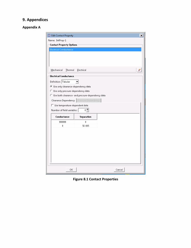
Figure 8.1 Contact Properties
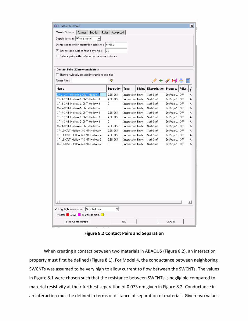
Figure 8.2 Contact Pairs and Separation
When creating a contact between two materials in ABAQUS (Figure 8.2), an interaction
property must first be defined (Figure 8.1). For Model 4, the conductance between neighboring
SWCNTs was assumed to be very high to allow current to flow between the SWCNTs. The values
in Figure 8.1 were chosen such that the resistance between SWCNTs is negligible compared to
material resistivity at their furthest separation of 0.073 nm given in Figure 8.2. Conductance in
an interaction must be defined in terms of distance of separation of materials. Given two values

of conductance with respective separation, ABAQUS will linearly interpolate the conductivity
between any two contact pairs with the interaction property. In Figure 8.2 where interfaces are
separated by 0.073 nm, the conductivity is determined to be 460E+3 Siemens (2.17 µΩ of
resistance). Where there is 0 nm separation the conductivity is 1E+6 Siemens (1 µΩ of
resistance). This was done to assume near-ideal contacts at the interfaces to neglect contact
resistances that may interfere with the skin effect.