Embed Size (px)
Citation preview

On the modeling and simulation of reaction-transferdynamics in semiconductor-electrolyte solar cells
Yuan He∗ Irene M. Gamba† Heung-Chan Lee‡ Kui Ren§
November 3, 2015
Abstract
The mathematical modeling and numerical simulation of semiconductor-electrolytesystems play important roles in the design of high-performance semiconductor-liquidjunction solar cells. In this work, we propose a macroscopic mathematical model, asystem of nonlinear partial differential equations, for the complete description of chargetransfer dynamics in such systems. The model consists of a reaction-drift-diffusion-Poisson system that models the transport of electrons and holes in the semiconductorregion and an equivalent system that describes the transport of reductants and oxi-dants, as well as other charged species, in the electrolyte region. The coupling betweenthe semiconductor and the electrolyte is modeled through a set of interfacial reactionand current balance conditions. We present some numerical simulations to illustratethe quantitative behavior of the semiconductor-electrolyte system in both dark andilluminated environments. We show numerically that one can replace the electrolyteregion in the system with a Schottky contact only when the bulk reductant-oxidant pairdensity is extremely high. Otherwise, such replacement gives significantly inaccuratedescription of the real dynamics of the semiconductor-electrolyte system.
Key words. Semiconductor-electrolyte system, reaction-drift-diffusion-Poisson system, semicon-ductor modeling, interfacial charge transfer, interface conditions, semiconductor-liquid junction,solar cell simulation, nano-scale device modeling.
AMS subject classifications 2000. 82D37, 34E05, 35B40, 78A57
1 Introduction
The mathematical modeling and simulation of semiconductor devices have been extensivelystudied in past decades due to their importance in industrial applications; see [1, 31, 35,
∗Department of Mathematics and ICES, University of Texas, Austin, TX 78712; Email:[email protected] .†Department of Mathematics and ICES, University of Texas, Austin, TX 78712; Email:
[email protected] .‡Department of Chemistry, University of Texas, Austin, TX 78712; Email: [email protected] .§Department of Mathematics and ICES, University of Texas, Austin, TX 78712; Email:
1
arX
iv:1
511.
0041
7v1
[m
ath.
AP]
2 N
ov 2
015

41, 44, 50, 51, 61, 77, 79] for overviews of the field and [9, 38, 76, 85] for more details onthe physics, classical and quantum, of semiconductor devices. In the recent years, the fieldhas been boosted significantly by the increasing need for simulation tools for designing effi-cient solar cells to harvest sunlight for clean energy. Various theoretical and computationalresults on traditional semiconductor device modeling are revisited and modified to accountfor new physics in solar cell applications. We refer interested readers to [28] for a summaryof various types of solar cells that have been constructed, to [46, 63] for simplified analyt-ical solvable models that have been developed, and to [19, 73, 54, 34] for more advancedmathematical and computational analysis of various models. Mathematical modeling andsimulation provide ways not only to improve our understanding of the behavior of the solarcells under experimental conditions, but also to predict the performance of solar cells withgeneral device parameters, and thus they enable us to optimize the performance of the cellsby selecting the optimal combination of these parameters.
One popular type of solar cells, besides those made of semiconductor p-n junctions, arecells made of semiconductor-liquid junctions. A typical liquid-junction photovoltaic solarcell consists of four major components: the semiconductor, the liquid, the semiconductor-liquid interface and the counter electrode; see a rough sketch in Fig. 1 (left). There are
many possible semiconductor-liquid combinations; see for instance, [25] for Si/viologen2+/+
junctions, [72] for n-type InP/Me2Fc+/0 junctions, and [28, Tab. 1] for a summary of manyother possibilities. The working mechanism of this type of cell is as follows. When sunlightis absorbed by the semiconductor, free conduction electron-hole pairs are generated. Theseelectrons and holes are then separated by an applied potential gradient across the device. Theseparation of the electrons and holes leads to electrical current in the cell and concentrationof charges on the semiconductor-liquid interface where electrochemical reactions and chargetransfer occur. We refer interested reader to [36, 37, 45] for physical principles and technicalspecifics of various types of liquid-junction solar cells.
Charge transport processes in semiconductor-liquid junctions have been studied in thepast by many investigators; see [53] for a recent review. The mechanisms of charge gen-eration, recombination, and transport in both the semiconductor and the liquid are nowwell understood. However, the reaction and charge transfer process on the semiconductor-liquid interface is far less understood despite the extensive recent investigations from bothphysical [32, 33, 52, 68] and computational [63, 82] perspectives. The objective of thiswork is to mathematically model this interfacial charge transfer process so that we couldderive a complete system of equations to describe the whole charge transport process in thesemiconductor-liquid junction.
To be specific, we consider here semiconductor-liquid junction with the liquid beingelectrolyte that contains reductant r, oxidant o and some other charged species that do notinteract with the semiconductor. We denote by Ω ⊂ Rd (d ≥ 1) the domain of interestwhich contains the semiconductor part ΩS and the electrolyte part ΩE. We denote byΣ ≡ ∂ΩE∩∂ΩS the interface between the semiconductor and electrolyte, ΓC the surface of thecurrent collector at the semiconductor end, and ΓA the surface of the counter (i.e., auxiliary)electrode. ΓS = ∂ΩS\(Σ∪ΓC) is the part of the semiconductor boundary that is neither theinterface Σ nor the contact ΓC, and ΓE = ∂ΩE\(Σ∪ΓA) the part of electrolyte that is neitherthe interface Σ nor the surface of the counter electrode ΓA. We denote by ν(x) the unit
2

ΓS
ΓS
ΓE
ΓE
ΣΓC ΓA Σ ΓA
Figure 1: Left: Sketch of main components in a typical semiconductor-liquid junction so-lar cell. Middle and Right: Two typical settings for semiconductor-electrolyte systems indimension two. The semiconductor S and the electrolyte E are separated by the interface Σ.
outer normal vector at a point x on the boundary of the domain ∂Ω = ΓC∪ΓS∪ΓA∪ΓE. Todeal with discontinuities of quantities across the interface Σ, we use Σ− and Σ+ to denotethe semiconductor and the electrolyte sides, respectively, of Σ. On the interface, we useν−(x) and ν+(x) to denote the unit normal vectors at x ∈ Σ pointing to the semiconductorand the electrolyte domains, respectively.
The rest of the paper is structured as follows. In the next three sections, we presentthe three main components of the mathematical model. We first model in Section 2 thedynamics of the electrons and holes in the semiconductor ΩS. We then model in Section 3the dynamics of the reductants and oxidants, as well as other charged species, in the elec-trolyte ΩE. In Section 4 we model the reaction-transfer dynamics on the interface Σ. Oncethe mathematical model has been constructed, we develop in Section 5 some numericalschemes for the numerical simulation of the device in simplified settings. We present somenumerical experiment in Section 6 where we exhibit the benefits of modeling the completesemiconductor-electrolyte system. Concluding remarks are offered in Section 7.
2 Transport of electrons and holes
The modeling of transport of free conduction electrons and holes in semiconductor deviceshas been well studied in recent decades [1, 31, 35, 41, 44, 61, 77, 79]. Many differentmodels have been proposed, such as the Boltzmann-Poisson system [6, 13, 17, 20, 27, 43,44, 60, 67, 74], the energy transport system [23, 30, 44] and the drift-diffusion-Poissonsystem [2, 14, 22, 21, 44, 61, 73, 75, 80, 83, 84]. For the purpose of computational efficiency,we employ the reaction-drift-diffusion-Poisson model in this work. Let us denote by (0, T ]the time interval in which we interested. The bipolar drift-diffusion-Poisson model can bewritten in the following form:
∂tρn +∇ · Jn = −Rnp(ρn, ρp) + γGnp(x), in (0, T ]× ΩS
∂tρp +∇ · Jp = −Rnp(ρn, ρp) + γGnp(x), in (0, T ]× ΩS
−∇ · (εSr∇Φ) =q
ε0[C(x) + αpρp + αnρn], in (0, T ]× ΩS.
(1)
3
with the fluxes of electrons and holes are given respectively by
Jn = −Dn∇ρn − αnµnρn∇Φ, Jp = −Dp∇ρp − αpµpρp∇Φ. (2)
Here ρn(t,x) and ρp(t,x) are the densities of the electrons and the holes, respectively, at timet and location x, and Φ(t,x) is the electrical potential. The notation ∂t denotes the derivativewith respect to t, while ∇ denotes the usual spatial gradient operator. The constant ε0 isthe dielectric constant in vacuum, and the function εSr (x) is the relative dielectric functionof the semiconductor material. The function C(x) is the doping profile of the device. Thecoefficients Dn (resp., Dp) and µn (resp., µp) are the diffusivity and the mobility of electrons(resp., holes). These parameters can be computed from the first principles of statisticalphysics. In some practical applications, however, they can be fitted from experimentaldata as well; see, for example, the discussion in [76]. The parameter q is the unit electriccharge constant, while αn = −1 and αp = 1 are the charge numbers of electrons and holes,respectively. The diffusivity and the mobility coefficients are related through the Einsteinrelations Dn = UT µn and Dp = UT µp with UT the thermal voltage at temperature T givenby UT = kB T /q, and kB being the Boltzmann constant.
2.1 Charge recombination and generation
The function Rnp(ρn, ρp) describes the recombination and generation of electron-hole pairsdue to thermal excitation. It represents the rate at which the electron-hole pairs are elim-inated through recombination (when Rnp > 0) or the rate at which electron-hole pairs aregenerated (when Rnp < 0). Due to the fact that electrons and holes are always recombinedand generated in pairs, we have the same rate function for the two species. To be specific,we consider in this work the Auger model of recombination that is based on interactionsbetween multiple electrons and holes, but we refer interested readers to [9, 29, 48, 61] fordiscussions on other popular recombination models such as the Shockley-Read-Hall (SRH)model and the Langevin model. The Auger model is relevant in cases where the carrierdensities are high (for instance in doped materials). It is expressed as
Rnp(ρn, ρp) = (Anρn + Apρp)(ρ2isc − ρnρp), (3)
where An and Ap are the Auger coefficients for electrons and holes respectively. For givenmaterials, An and Ap can be measured by experiments. The parameter ρisc is the intrinsiccarrier density that is often calculated from the following formula (see [48]):
ρisc =√NcNv
( T300
)1.5
e− Eg
2kBT (4)
where the band gap Eg = Eg0 − αT 2/(T + β) with Eg0 the band gap at T = 0K (Eg0 =1.17q for silicon for instance), α = 4.73 10−4q, and β = 636. The parameters Nc andNv are effective density of states in the conduction and the valence bands, respectively, atT = 300K.
When the semiconductor device is illuminated by sunlight, the device absorbs photonenergy. The absorbed energy creates excitons (bounded electron-hole pairs). The excitons
4

are then separated into free electrons and holes which can then move independently. Thisgeneration of free electron-hole pairs is modeled by the source function Gnp(x) in the trans-port equation (1). Once again, due to the fact that electrons and holes are always generatedin pairs, the generating functions are the same for electrons and holes. We take a modelthat assumes that photons travel across the device in straight lines. That is, we assume thatphotons do not get scattered by the semiconductor material during their travel inside thedevice. This is a reasonable assumption for small devices that have been utilized widely [45].Precisely, the generation of charges is given as
Gnp(x) =
σ(x)G0(x0)e−
∫ s0 σ(x0+s′θ0)ds′ , if x = x0 + sθ0
0, otherwise(5)
where x0 ∈ ΓS is the incident location, θ0 is the incident direction, σ(x) is the absorptioncoefficient (integrated over the usable spectrum), and G0(x0) is the surface photon flux atx0. The control parameter γ ∈ 0, 1 in (1) is used to turn on and off the illuminationmechanism, and γ = 0 and γ = 1 are the dark and illuminated cases, respectively.
2.2 Boundary conditions
We have to supply boundary conditions for the equations in the semiconductor domain. Thesemiconductor boundary, besides the interface Σ, is split into two parts, the current collectorΓC and the rest. The boundary condition on the current collector is determined by the typeof contacts formed there. There are mainly two types of contacts, the Ohmic contact andthe Schottky contact.
Dirichlet at Ohmic contacts. Ohmic contacts are generally used to model metal-semiconductorjunctions that do not rectify current. They are appropriate when the Fermi levels in themetal contact and adjacent semiconductor are aligned. Such contacts are mainly used tocarry electrical current out and into semiconductor devices, and should be fabricated withlittle (or ideally no) parasitic resistance. Low resistivity Ohmic contacts are also essentialfor high-frequency operation. Mathematically, Ohmic contacts are modeled by Dirichletboundary conditions which can be written as [9, 48, 61, 65]
ρn(t,x) = ρen(x), ρp(t,x) = ρep(x), on (0, T ]× ΓC,Φ(t,x) = ϕbi + ϕapp, on (0, T ]× ΓC,
(6)
where ϕbi and ϕapp are the built-in and applied potentials, respectively. The boundaryvalues ρen, ρep for the Ohmic contacts are calculated following the assumptions that thesemiconductor is in stationary and equilibrium state and that the charge neutrality conditionholds. This means that right-hand-side of the Poisson equation disappears so that
C + ρep − ρen = 0. (7)
Thermal equilibrium implies that generation and recombination balance out, so Rnp = 0 atOhmic contacts. This leads to the mass-action law, between the density of electrons andholes:
ρenρep − ρ2
isc = 0. (8)
5

The system of equations (7) and (8) admit a unique solution pair (ρn, ρp), which is given by
ρen(t,x) =1
2(√C2 + 4ρ2
isc + C), ρep(t,x) =1
2(√C2 + 4ρ2
isc − C). (9)
These densities result in a built-in potential that can be calculated as
ϕbi = UT ln(ρen/ρisc). (10)
Note that due to the fact that the doping profile C varies in space, these boundary valuesare different on different part of the boundary.
Robin (or mixed) at Schottky contacts. Schottky contacts are used to model metal-semiconductor junctions that have rectifying effects (in the sense that current flow throughthe contacts is rectified). They are appropriate for contacts between a metal and a lightlydoped semiconductor. Mathematically, at a Schottky contact, Robin- (also called mixed-)type of boundary conditions are imposed for the n- and p-components, while Dirichlet-typeof conditions are imposed for the Φ-component. More precisely, these boundary conditionsare [9, 48, 61, 65]:
ν · Jn(t,x) = vn(ρn − ρen)(x), ν · Jp(t,x) = vp(ρp − ρep)(x), on (0, T ]× ΓC,Φ(t,x) = ϕStky + ϕapp, on (0, T ]× ΓC.
(11)
Here the parameters for the Schottky barrier are the recombination velocities vn and vp, andthe height of the potential barrier, ϕStky, which depends on the materials of the semicon-ductor and the metal in the following way:
ϕStky =
Φm − χ, n-typeEg
q− (Φm − χ), p-type
(12)
where Φm is the work function, i.e., the potential difference between the Fermi energy andthe vacuum level, of the metal and χ is the electron affinity, i.e., the potential differencebetween the conduction band edge and the vacuum level. Eg is again the band gap. Thevalues of the parameters vn, vp, Φm, and χ are given in Tab. 1 of Section 6.
Neumann at insulating boundaries. On the part of the semiconductor boundary thatis not the current collector, it is natural to impose insulating boundary conditions whichensures that there is no charge or electrical currents through the boundary. The conditionsare
ν ·Dn∇ρn(t,x) = 0, ν ·Dp∇ρp(t,x) = 0, on (0, T ]× ΓS,ν · εSr∇Φ(t,x) = 0, on (0, T ]× ΓS.
(13)
In solar cell applications, part of the boundary ΓS is where illumination light enters thesemiconductor.
We finish this section with the following remarks. It is generally believed that theBoltzmann-Poisson model [44] is a more accurate model for charges transport in semicon-ductors. However, the Boltzmann-Poisson model is computationally more expensive to solve
6

and analytically more complicated to analyze. The drift-diffusion-Poisson model (1) can beregarded as a macroscopic approximation to the Boltzmann-Poisson model. The validity ofthe drift-diffusion-Poisson model can be justified in the case when the mean free path of thecharges is very small compared to the size of the device and the potential drop across thedevice is small (so that the electric field is not strong); see, for instance, [7, 12, 14, 15, 44]for such a justification.
3 Charge transport in electrolytes
We now present the equations for the reaction-transport dynamics of charges in an elec-trolyte. To be specific, we consider here only electrolytes that contain reductant-oxidantpairs (denoted by r and o) that interact directly with the semiconductor through electronstransfer (which we will model in the next section), and N other charged species (denoted byj = 1, ..., N) that do not interact directly with the semiconductor through electron transfer.We also limit our modeling efforts to reaction, recombination, transport, and diffusion ofthe charges. Other more complicated physical and chemical processes are neglected.
We model the charge transport dynamics in electrolyte again with a set of reaction-drift-diffusion-Poisson equations. In the electrochemistry literature, this mathematical descrip-tion of the dynamics is often called the Poisson-Nernst-Planck theory [4, 8, 24, 26, 40, 57,47, 58, 62, 59, 69, 78, 81]. Let us denote by ρr(t,x) the density of the reductants, by ρo(t,x)the density of the oxidants, and by ρj (1 ≤ j ≤ N) the density of the other N charge species.Then these densities solve the following system that is of the same form as (1):
∂tρr +∇ · Jr = +Rro(ρr, ρo), in (0, T ]× ΩE,∂tρo +∇ · Jo = −Rro(ρr, ρo), in (0, T ]× ΩE,∂tρj +∇ · Jj = Rj(ρ1, · · · , ρN), 1 ≤ j ≤ N in (0, T ]× ΩE,
−∇ · εEr∇Φ =q
ε0(αoρo + αrρr +
∑Nj=1 αjρj), in (0, T ]× ΩE.
(14)
with the fluxes given respectively by
Jr = −Dr∇ρr − αrµrρr∇Φ, Jo = −Do∇ρo − αoµoρo∇ΦJj = −Dj∇ρj − αjµjρj∇Φ, 1 ≤ j ≤ N
(15)
where again the diffusion coefficient Dr (resp., Do and Dj) is related to the mobility µr (resp.,µo and µj) through the Einstein relation Dr = UT µr (resp., Do = UT µo and Dj = UT µj).The parameters αo, αr and αj (1 ≤ j ≤ N) are the charge numbers of the correspondingcharges species. Depending on the type of the redox pairs in the electrolyte, the chargenumbers can be different; see, for instance, [28] for a summary of various types of redoxelectrolytes that have been developed.
Let us remark that in the above modeling of the dynamics of reductant-oxidant pair, wehave implicitly assumed that the electrolyte, in which the redox pairs live, is not perturbed bycharge motions. In other words, there is no macroscopic deformation of the electrolyte thatcan occur. If this is not the case, we have to introduce the equations of fluid dynamics, mainlythe Navier-Stokes equation, for the fluid motion, and add an advection term (with advectionvelocity given by the solution of the Navier-Stokes equation) in the current expressionsin (15). The dynamics will thus be far more complicated.
7

3.1 Charge generation through reaction
The reaction mechanism between the oxidants and the reductants is modeled by the reactionrate function Rro. Note that the elimination and generation of the redox pairs are differentfrom those of the electrons and holes. An oxidant is eliminated (resp., generated) when areductant is generated (resp., eliminated) and vice versa. This is the reason why there isa negative sign in front of the function Rro in the second equation of (14). The oxidation-reduction reaction requires free electrons which are only available through the semiconductor.Therefore this reaction occurs mainly on the semiconductor-electrolyte interface. We thusassume in general that there is no oxidation-reduction reaction in the bulk electrolyte; thatis,
Rro(ρr, ρo) = 0, in (0, T ]× ΩE. (16)
This is what we adopt in the simulations of Section 6. The oxidation-reduction reaction onthe interface Σ will be modeled in the next section.
The reactions among other charged species in the electrolyte are modeled by the reactionrate functions Rj (1 ≤ j ≤ N). The exact forms of these rate functions can be derivedfollowing the law of mass action once the types of reactions among the charged speciespresented in the electrolyte are known. We refer to [11, 18] for the rate functions for variouschemical reactions.
3.2 Boundary conditions
It is generally assumed that the interface of semiconductor and electrolyte is far from thecounter electrode. Therefore the values for the densities of redox pairs on the electrode ΓA
are set as their bulk values. Mathematically, this means that Dirichlet boundary conditionshave to be imposed:
ρr(t,x) = ρ∞r (x), ρo(t,x) = ρ∞o (x), on (0, T ]× ΓA,ρj(t,x) = ρ∞j (x), 1 ≤ j ≤ N, Φ(t,x) = ϕA
app, on (0, T ]× ΓA,(17)
where ρ∞r and ρ∞o are the bulk concentration of the respective species, and ϕAapp is the applied
potential on the counter electrode. The values of these parameters are given in Tab. 1 inSection 6.
On the rest of the electrolyte boundary, ΓE, we impose again insulating boundary con-ditions:
ν ·Dr∇ρr(t,x) = 0, ν ·Do∇ρo(t,x) = 0, on (0, T ]× ΓE,ν ·Dj∇ρj(t,x) = 0, 1 ≤ j ≤ N, ν · εEr∇Φ(t,x) = 0, on (0, T ]× ΓE,
(18)
4 Interfacial reaction and charge transfer
In order to obtain a complete mathematical model for the semiconductor-electrolyte system,we have to couple the system of equations in the semiconductor with those in the electrolytethrough interface conditions that describe the interfacial charge transfer process.
8

4.1 Electron transfer between electron-hole and redox
The microscopic electrochemical processes on the semiconductor-electrolyte interface canbe very complicated, depending on the types of semiconductor materials and electrolytesolutions. There is a vast literature in physics and chemistry devoted to the subject; see,for instance, [5, 32, 33, 45, 52, 53, 63, 68, 70, 71, 82] and references therein. We are onlyinterested in deriving macroscopic interface conditions that are consistent with the dynam-ics of charge transport in the semiconductor and the electrolyte modeled by the equationsystems (1) and (14). Without attempting to construct models in the most general cases,we focus here on oxidation-reduction reactions described by the following process,
Ox|α0|+ + e−(S) Red|αr|−, (19)
with αo − αr = 1, Ox and Red denoting respectively the oxidant and the reductant, ande−(S) denoting an electron from the semiconductor. Experimental studies semiconductor-
electrolyte interface with this type of reaction can be found in [25] for Si/viologen2+/+
interfaces and in [72] for n-type InP/Me2Fc+/0 interfaces.The changes of the concentrations of the redox pairs on Σ+, after taking into account
the conservation of ρr + ρo, can be written respectively as:
dρrdt
= kfρo − kbρr anddρodt
= kbρr − kfρo, (20)
where kf and kb are the pseudo first-order forward and backward reaction rates, respectively.The forward reaction rate kf is proportional to the product of the electron transfer rate ketthrough the interface and the density of the electrons on Σ−. The backward reaction ratekb is proportional to the product of the hole transfer rate kht and the density of the holeson Σ−. More precisely, we have [32, 33, 53, 63]:
kf (t,x) = ket(x)(ρn − ρen) and kb(t,x) = kht(x)(ρp − ρep), on (0, T ]× Σ. (21)
The changes of the concentrations lead to, following the relations ν+ · Jr = −dρrdt
and
ν+·Jo = −dρodt
, fluxes of redox pairs through the interface that can be expressed as follows [32,33, 53, 63]:
ν+ · Jr = kht(x)(ρp − ρep)ρr(t,x)− ket(x)(ρn − ρen)ρo(t,x), on (0, T ]× Σν+ · Jo = −kht(x)(ρp − ρep)ρr(t,x) + ket(x)(ρn − ρen)ρo(t,x), on (0, T ]× Σ
(22)
where the unit normal vector ν+ points toward the electrolyte domain.The fluxes of the redox pairs from the interface given in (22) consists of two contributions:
the flux induced from the transfer of electrons from the semiconductor to the electrolyte,often called the cathodic current after being brought up to the right dimension, ν+ ·Jn, andthe flux induced from the transfer of electrons from the electrolyte to the conduction band,often called the anodic current after being brought up to the right dimension, ν+ · Jp:
ν+ · Jn = (−ν−) · Jn = −ket(x)(ρn − ρen)ρo(t,x), on (0, T ]× Σν+ · Jp = (−ν−) · Jp = −kht(x)(ρp − ρep)ρr(t,x), on (0, T ]× Σ
(23)
9

The interface conditions (22) and (23) can now be supplied to the semiconductor equa-tions in (1) and the redox equations in (14) respectively. The values of the electron andhole transfer rates, ket and kht, in the interface conditions can be calculated approximatelyfrom the first principles of physical chemistry [5, 32, 33, 45, 52, 63, 68, 70, 71, 82]. The-oretical analysis shows that both parameters can be approximately treated as constant;see, for instance, [53] for a summary of various ways to approximate these rates. Thedependence of the forward and reverse reaction rates, kf and kb, on the electric poten-tial Φ is encoded in the electron and hole densities (i.e. ρn and ρp) on the interface. Infact, we can recover the commonly used Butler-Volmer model [3, 66] from our model asfollows. Consider a one-dimensional semiconductor-electrolyte system (just for the pur-poses of presentation). At the equilibrium of the system, the net reaction rate is zero, i.eν+ · Jo = −ν+ · Jr = ν+ · Jn − ν+ · Jp = kfρo − kbρr = 0 on Σ+. This leads to, by theexpression for the fluxes (15), the following relation between densities of redox pairs and theelectric potential:
ρr = ρer exp
(Φ− Φe
UT
), ρo = ρeo exp
(Φ− Φe
UT
)(24)
where we have used the Einstein relations Dr = UT µr and Do = UT µo, Φe is the equilibriumpotential of the electrolyte, and ρer, ρ
eo are the corresponding densities. Therefore at the
system equilibrium the forward and reverse reaction rates satisfy:
kfkb
=ρoρr
=ρeoρer
exp
(−2(Φ− Φe)
UT
). (25)
This implies that
− 1
2UT
(d ln kfdΦ
− d ln kbdΦ
)= 1. (26)
If we define the reductive symmetry factor (related to the forward reaction) α = −UT2
d ln kfdΦ
,
the above relation then implies that UT2d ln kbdΦ
= 1 − α. Moreover, the definition leads tokf = k0 exp(−αη(Φ−Φe)) and kb = k0 exp((1−α)η(Φ−Φe)) with η = 2/UT , where k0 is thestandard rate constant. We can therefore have the following Butler-Volmer model [3, 42, 66]for the interface flux:
ν+ · Jo = −ν+ · Jr = k0[e−αη(Φ−Φe)ρo(t,x)− e(1−α)η(Φ−Φe)ρr(t,x)
]. (27)
4.2 Interface conditions for nonredox charges
For the N charged species in the electrolyte that do not interact directly with the semicon-ductor through electron transfer, we impose insulating boundary conditions on the interface:
ν− · Jj = 0, 1 ≤ j ≤ N, on (0, T ]× Σ (28)
We need to specify the interface condition for the electric potential as well. This is doneby requiring Φ to be continuous across the interface and have continuous flux. Let us denote
10

by Σ+ and Σ− the semiconductor and the electrolyte sides, respectively, of Σ; then theconditions on the electric potential are given by
[Φ]Σ ≡ Φ|Σ−−Φ|Σ+ = 0, [εr∂Φ
∂ν]Σ ≡
(εEr∂Φ
∂ν
)|Σ−−(εSr∂Φ
∂ν
)|Σ+
= 0, on (0, T ]×Σ. (29)
Note that these continuity conditions would not prevent large the electric potential dropsacross a narrow neighborhood of the interface, as we will see in the numerical simulations.
The interface conditions that we constructed in this section ensure the conservation ofthe total flux J across the interface. To check that we recall that the total flux in the systemis given as [11, 26, 39, 79]
J(x) =
αpJp + αnJn, x ∈ S
αoJo + αrJr +∑N
j=1 αjJj, x ∈ E(30)
Using (22), (23), (28) and the fact that αo − αr = 1, we verify that ν+ · J|Σ− = ν+ · J|Σ+ .
5 Numerical discretization
The drift-diffusion-Poisson equations in (1) and (14), together with the boundary conditionsgiven in (6) (resp., (11)), (13), (17), (18), and the interface conditions (22), (23), (28),and (29) form a complete mathematical model for the transport of charges in the system ofsemiconductor-electrolyte for solar cell simulations. We now present a numerical procedureto solve the system.
5.1 Nondimensionalization
We first introduce the following characteristic quantities in the simulation regarding thedevice and its physics. We denote by l∗ the characteristic length scale of the device, t∗ thecharacteristic time scale, Φ∗ the characteristic voltage, and C∗ the characteristic density. Thevalues (and units) for these characteristic quantities are respectively (see [48, 50, 51, 65, 70]),
l∗ = 10−4 (cm), t∗ = 10−12 (s), Φ∗ = UT (V), C∗ = 1016 (cm−3). (31)
We now rescale all the physical quantities. For any quantity Q, we use Q′ to denote itsrescaled version. To be specific, we introduce the rescaled Debye lengths in the semiconduc-tor and electrolyte regions, respectively, as
λS =1
l∗
√Φ∗εS
qC∗, and λE =
1
l∗
√Φ∗εE
qC∗.
We also introduce the following rescaled quantities,
t′ = t/t∗, x′ = x/l∗, Φ′ = Φ/Φ∗, ρ′z = ρz/C∗, z ∈ n, p, r, o, 1, · · · , N
R′np(ρ′n, ρ′p) =
t∗
C∗Rnp(C
∗ρ′n, C∗ρ′p), R′ro(ρ
′r, ρ′o) =
t∗
C∗Rro(C
∗ρ′r, C∗ρ′o)
R′j(ρ′1, · · · , ρ′N) =
t∗
C∗Rj(C
∗ρ′1, · · · , C∗ρ′N), 1 ≤ j ≤ N
G′0 =t∗
l∗C∗G0, D′z = Dz
t∗
l∗2, µ′z = µz
t∗Φ∗
l∗2, z ∈ n, p, r, o, 1, · · · , N
T ′ = T/t∗, C ′ = C/C∗, A′p = t∗C∗2A′p, A′n = t∗C∗2An, ρisc = ρisc/C∗
(32)
11

for the model equations (1) and (14), and the following rescaled variables,
k′et = kett∗C∗/l∗, k′ht = khtt
∗C∗/l∗, v′n = vnt∗/l∗, v′p = vpt
∗/l∗
ϕ′bi = ϕbi/Φ∗, ϕ′app = ϕapp/Φ
∗, ϕ′Stky = ϕStky/Φ∗, ϕA′
app = ϕAapp/Φ
∗
ρe′n = ρen/C
∗, ρe′p = ρep/C
∗, ρ′∞z = ρ∞z /C
∗, z ∈ r, o, 1, · · · , N(33)
for the boundary and interface conditions described in (6), (11), (13), (17), (18), (22), (23), (28),and (29).
We can now summarize the mathematical model in rescaled (nondimensionalized) formas the following,
∂t′ρ′n −∇ · (D′n∇ρ′n + αnµ
′nρ′n∇Φ′) = −R′np(ρ′n, ρ′p) + γG′np, in (0, T ′]× ΩS,
∂t′ρ′p −∇ · (D′p∇ρ′p + αpµ
′pρ′p∇Φ′) = −R′np(ρ′n, ρ′p) + γG′np, in (0, T ′]× ΩS,
−∇ · λ2S∇Φ′ = C ′ + αpρ
′p + αnρ
′n, in (0, T ′]× ΩS
Φ′ = ϕ′bi + ϕ′app(or Φ′ = ϕ′Stky + ϕ′app), ρ′n = ρe′n , ρ′p = ρe
′p on (0, T ′]× ΓC
ν · εSr∇Φ′ = 0, ν ·D′n∇ρ′n = 0, ν ·D′p∇ρ′p = 0 on (0, T ′]× ΓS
Φ′ = ϕA′
app, on (0, T ′]× ΓA
ν · εEr∇Φ′ = 0, on (0, T ′]× ΓE
(34)
for the transport dynamics in the rescaled semiconductor domain ΩS, as the following,
∂t′ρ′r −∇ · (D′r∇ρ′r + αrµ
′rρ′r∇Φ′) = +R′ro(ρ
′r, ρ′o), in (0, T ′]× ΩE,
∂t′ρ′o −∇ · (D′o∇ρ′o + αoµ
′oρ′o∇Φ′) = −R′ro(ρ′r, ρ′o), in (0, T ′]× ΩE,
∂t′ρ′j −∇ · (D′j∇ρ′j + αjµ
′jρ′j∇Φ′) = R′j(ρ
′1, · · · , ρ′N), in (0, T ′]× ΩE,
−∇ · λ2E∇Φ′ = αoρ
′o + αrρ
′r +
∑Nj=1 αjρ
′j, in (0, T ′]× ΩE
ρ′r = ρ′∞r , ρ′o = ρ
′∞o , ρ′j = ρ
′∞j , on (0, T ′]× ΓA
ν ·D′r∇ρ′r = 0, ν ·D′o∇ρ′o = 0, ν ·D′j∇ρ′j = 0, on (0, T ′]× ΓE
(35)
for the transport dynamics in the (rescaled) electrolyte domain ΩE, and as the following,
[Φ′]Σ = 0, [εr∂Φ′
∂ν]Σ = 0, ν ·D′j∇ρ′j = 0 on (0, T ′]× Σ
ν+ · J′n = −k′et(ρ′n − ρe′n )ρ′o, ν+ · J′p = −k′ht(ρ′p − ρe
′p )ρ′r, on (0, T ′]× Σ
ν · J′r = −ν · J′o = k′ht(ρ′p − ρe
′p )ρ′r − k′et(ρ′n − ρe
′n )ρ′o, on (0, T ′]× Σ
(36)
for the dynamics on the interface Σ. Here the rescaled Auger generation-recombination rateR′np takes exactly the same form as in (3), i.e.,
R′np(ρ′n, ρ′p) = (A′nρ
′n + A′pρ
′p)(ρ
′2isc − ρ′nρ′p), (37)
and the rescaled photon illumination function G′np takes the form
G′np(x′) =
σ′(x′)G′0(x′0) exp
(−∫ s
0σ′(x′0 + sθ0)ds
), if x′ = x′0 + sθ0
0, otherwise(38)
In the rest of the paper, we will work on the numerical simulations of the semiconductor-electrolyte system based on the above nondimensionalized systems (34) and (35).
12

5.2 Time-dependent discretization
For the numerical simulations in this paper, we discretize the time-dependent systems ofreaction-drift-diffusion-Poisson equations (34) and (35) by standard finite difference methodin both spatial and temporal variables. In the spatial variable, we employ a classical upwinddiscretization of the advection terms (such as∇Φ′·∇ρ′n) to ensure the stability of the scheme.To avoid solving nonlinear systems of equations in each time step (since the models (34)and (35) are nonlinear), we employ the forward Euler scheme for the temporal variable.Since this is a first-order scheme and is explicit, we do not need to perform any nonlinearsolve in the solution process, as long as we can supply the right initial conditions. We areaware that there are many efficient solvers for similar problems that have been developed inthe literature; see, for instance, [86].
To solve stationary problems, we can evolve the system for a long time so that the systemreaches its stationary state. We use the magnitude of the relative L2 update of the solutionas the stopping criterion. An alternative, in fact more efficient, way to solve the nonlinearsystem is the following iterative scheme.
5.3 A Gummel-Schwarz iteration for stationary problems
This method combines domain decomposition strategies with nonlinear iterative schemes.We decompose the system naturally into two subsystems, the semiconductor system and theelectrolyte system. We solve the two subsystem alternatively and couple them with the in-terface condition. This is the Schwarz decomposition strategy that has been used extensivelyin the literature; see [16, 64] for similar domain decomposition strategies in semiconductorsimulation. To solve the nonlinear equations in each sub-problem, we adopt the Gummeliteration scheme [6, 10, 49]. This scheme decomposes the drift-diffusion-Poisson system intoa drift-diffusion part and a Poisson part and then solves the two parts alternatively. Thecoupling then comes from the source term in the Poisson equation. Our algorithm, in theform of solving the stationary problem, takes the following form.
GUMMEL-SCHWARZ ALGORITHM.
[1] Gummel step k = 0, construct initial guess ρ′0n , ρ′0p , ρ
′0r , ρ
′0o , ρ
′0j Nj=1
[2] Gummel step k ≥ 1:
– Solve the Poisson problem for Φ′k in ΩE∪ΩS using the densities ρ
′k−1n , ρ
′k−1p , ρ
′k−1r ,
ρ′k−1o , and ρ′k−1
j Nj=1:
−∇ · λ2S∇Φ
′k = C ′ + αpρ′k−1p + αnρ
′k−1n , in ΩS
−∇ · λ2E∇Φ
′k = αoρ′k−1o + αrρ
′k−1r +
∑Nj=1 αjρ
′k−1j , in ΩE
Φ′k = ϕ′bi + ϕ′app, or Φ
′k = ϕ′Stky + ϕ′app, on ΓC
ν · εSr∇Φ′k = 0, on ΓS
Φ′k = ϕA′
app, on ΓA
ν · εEr∇Φ′k = 0, on ΓE
[Φ′k]Σ = 0, [εr
∂Φ′k
∂ν]Σ = 0, on Σ
(39)
13

– Solve for ρ′kn , ρ
′kp , ρ
′kr , ρ
′ko , ρ
′kj Nj=1 as limits of the following iteration:
[i] Schwarz step ` = 0: construct guess (ρ′k,0n , ρ
′k,0p , ρ
′k,0r , ρ
′k,0o , ρ
′k,0j N1 )
[ii] Schwarz step ` ≥ 1: solve sequentially
∇ · (−D′n∇ρ′k,`n + αnµ
′nρ′k,`n ∇Φ
′k) = −R′np(ρ′k,`n , ρ
′k,`p ) + γG′np, in ΩS
∇ · (−D′p∇ρ′k,`p + αpµ
′pρ′k,`p ∇Φ
′k) = −R′np(ρ′k,`n , ρ
′k,`p ) + γG′np, in ΩS
ρ′k,`n = ρe
′n , ρ
′k,`p = ρ
′ep , on ΓC
ν ·D′n∇ρ′k,`n = 0, ν ·D′p∇ρ
′k,`p = 0, on ΓS
ν+ · J′k,`n = −k′et(ρ′k,`n − ρe
′n )ρ
′k,`−1o , ν+ · J′k,`p = −k′ht(ρ
′k,`p − ρe
′p )ρ
′k,`−1r , on Σ
(40)and
∇ · (−D′r∇ρ′k,`r + αrµ
′rρ′k,`r ∇Φ
′k) = +R′ro(ρ′k,`r , ρ
′k,`o ), in ΩE
∇ · (−D′o∇ρ′k,`o + αoµ
′oρ′k,`o ∇Φ
′k) = −R′ro(ρ′k,`r , ρ
′k,`o ), in ΩE
∇ · (−D′j∇ρ′k,`j + αjµ
′jρ′k,`j ∇Φ
′k) = Rj(ρk,`1 , · · · , ρ
′k,`N ), in ΩE
ρ′k,`r = ρ
′∞r , ρ
′k,`o = ρ
′∞o , ρ
′k,`j = ρ
′∞j , on ΓA
ν ·D′r∇ρ′k,`r = 0, ν ·D′o∇ρ
′k,`o = 0, ν ·D′j∇ρ
′k,`j = 0, on ΓE
ν · J′k,`r = −ν · J′k,`o = k′ht(ρ′k,`p − ρe
′p )ρ
′k,`r − k′et(ρ
′k,`n − ρe
′n )ρ
′k,`o , on Σ
ν ·D′j∇ρ′k,`j = 0, 1 ≤ j ≤ N on Σ.
(41)
[iii] If convergence criteria satisfied, stop; otherwise, set ` = `+ 1 and go to [ii].
[3] If convergence criteria satisfied, stop; Otherwise, set k = k + 1 and go to step [2].
Note that since (40) and (41) are solved sequentially, we are able to replace the ρ′k,`−1n and
ρ′k,`−1p terms in (41) in the boundary conditions on Σ with ρ
′k,`n and ρ
′k,`p respectively. This
slightly improves the speed of convergence of the numerical scheme. If the mathematicalsystem is well-posed, the convergence of this iteration can be established following the linesof work in [55, 56]. The details will be in a future work.
5.4 Computational issues
Initial conditions. To solve the time-dependent problem, we need to supply the systemwith appropriate initial conditions. Our initial conditions are given only for the densities.The initial condition on the potential is obtained by solving the Poisson equation with appro-priate boundary conditions using the initial densities. That is done by solving problem (39).
Stiffness of the system. One major issue in the numerical solution of the mathematicalmodel is the stiffness of the system across the interface, caused by the large contrast betweenthe magnitudes of the densities in the semiconductor and electrolyte domains. Physicallythis leads to the formation of boundary layers of charge densities local to the interface; see,for instance, discussions in [3, 63]. To capture the sharp transition at the interface, we haveto use finer finite difference grids around the interface.
14

Computation of stationary states. The Gummel-Schwarz iteration is attractive whenstationary state solutions are to be sought since it is computationally much more efficientthan the time-stepping method. However, due to the nonlinearity of the system, multiplesolutions could exist, as illustrated, for instance, in [84] in similar settings. Starting fromdifferent initial guesses for the nonlinear solver could lead us to different solutions (andsome of them could be unphysical). The time-stepping scheme, however, will lead us to thedesired steady state for any given initial state. We can combine the two methods. For agiven initial state, we use the time-stepping scheme to evolve the system for some time, sayT ′ (which we select empirically as a time when the fastest initial evolution of the solutionhas passed); we then use the solution at T ′ as the initial guess for the Gummel-Schwarziteration to find the corresponding steady state solution. In our numerical simulations, wedid not observe the existence of multiple steady states. However, this is an issue to keep inmind when more complicated (for instance multidimensional) simulations are performed.
6 Numerical simulations
We present some numerical simulations based on the mathematical model that we haveconstructed for the semiconductor-electrolyte system.
6.1 General setup for the simulations
To simplify the numerical computation, we assume some symmetry in the semiconductor-electrolyte system so that we can reduce the problem to one dimension. We showed in Fig. 1(middle and right) two typical two-dimensional systems where such dimension reductionscan be performed. In the first case, if we assume that the system is invariant in the directionparallel to the current collector, then we have a one-dimensional system in the direction thatis perpendicular to the current collector. In the second setting, we have a radially symmetricsystem that is invariant in the angular direction in the polar coordinate. The system canthen be regarded as a one-dimensional system in the radial direction.
In all the simulations we have performed, we use an n-type semiconductor to constructthe semiconductor-electrolyte system. We also select the electrolyte such that the chargenumbers αo − αr = 1. Furthermore, we assume in our simulation that the reductants andoxidants are the only charges in the electrolyte. Therefore the equations for ρ′j (1 ≤ j ≤ N)are dropped. In Tab. 1, we list the values of all the model parameters that we use in thesimulations. They are mainly taken from [9, 48, 76, 85] and references therein. These valuesmay depend on the materials used to construct the system and the temperature of thesystem (which we set to be T = 300K). They can be tuned to be more realistic by carefulcalibrations.
We perform simulations on two devices of different sizes. The two devices are designedto mimic a large (Device I) and small (Device II) nano- to micro-scale solar cell buildingblock, as follows.
Device I. The device is contained in Ω = (−1.0, 1.0) with the semiconductor ΩS = (−1.0, 0)and ΩE = (0, 1.0) separated by the interface Σ located at x′ = 0. The semiconductor
15

Parameter Value Unit Parameter Value Unitq 1.6× 10⁻¹⁹ [A s] kB 8.62× 10⁻⁵ q [J K−1]ε0 8.85× 10⁻¹⁴ [A s V−1 cm−1] εSr 11.9µn 1500 [cm2 V−1 s−1] µp 450 [cm2 V−1 s−1]An 2.8× 10⁻³¹ [cm6 s−1] Ap 9.9× 10⁻³² [cm6 s−1]Nc 2.80× 10¹⁹ [cm−3] Nv 1.04× 10¹⁹ [cm−3]vn 5× 10⁶ [cm s−1] vp 5× 10⁶ [cm s−1]Φm 2.4 [V] χ 1.2 [V]ket 1× 10⁻²¹ [cm4 s−1] kht 1× 10⁻¹⁷ [cm4 s−1]µo 2× 10⁻¹ [cm2 V−1 s−1] µr 0.5× 10⁻¹ [cm2 V−1 s−1]εEr 1000 G0 1.2× 10¹⁷ [cm−2s−1]
Table 1: Values of physical parameters used in the numerical simulations. The numbers aregiven in unit of cm, s, V, A.
boundary ΓS is thus at the point x′ = −1.0, while the electrolyte boundary ΓE is at thepoint x′ = 1.0.
Device II. The device is contained in Ω = (−0.2, 0.2) with the semiconductor ΩS = (−0.2, 0)and ΩE = (0, 0.2) separated by the interface Σ located at x′ = 0. The semiconductorboundary ΓS is thus at the point x′ = −0.2, while the electrolyte boundary ΓE is at thepoint x′ = 0.2.
6.2 General dynamics of semiconductor-electrolyte systems
We now present simulation results on general dynamics of the semiconductor-electrolytesystems we have constructed. We perform the simulations using the first system, i.e., DeviceI. General parameters in the simulations are listed in Tab. 1. We consider three differentcases.
Case I (a). In this simulation, we show typical dynamics of the semiconductor-electrolytesystem in dark and illuminated cases. We consider the case when the densities of thereductant-oxidant pair are very high compared to the densities of the electron-hole pair.Specifically, we take ρ
′∞r = 30.0, ρ
′∞o = 29.0. The system starts from the initial conditions:
ρ′0n = 2, ρ
′0p = 1.0, ρ0
r = ρ′∞r , and ρ
′0o = ρ
′∞o . We first perform simulation for the dark case,
i.e., when the parameter γ = 0. In the left column of Fig. 2, we show the distributions ofthe charge densities, electric field and total fluxes in the semiconductor and the electrolyteat time t′ = 0.05. The corresponding distributions at stationary state are shown in the rightcolumn.
We now repeat the simulation in the illuminated environment by setting the parameterγ = 1. In this case, the surface photon flux is set as G′0 = 1.2×10⁻⁷ to mimic a solar spectralirradiance with air mass 1.5. The simulation results are presented in Fig. 3. In both thedark and illuminated cases shown here, the applied potential bias is 19.3, and Ohmic contact(i.e. Dirichlet condition) is assumed at the left end of the semiconductor.
16

−1 −0.8 −0.6 −0.4 −0.2 0 0.2 0.4 0.6 0.8 10
20
40Densities
−1 −0.8 −0.6 −0.4 −0.2 0 0.2 0.4 0.6 0.8 1−20
−10
0Electric field
−1 −0.8 −0.6 −0.4 −0.2 0 0.2 0.4 0.6 0.8 1−0.2
0
0.2Currents
−1 −0.8 −0.6 −0.4 −0.2 0 0.2 0.4 0.6 0.8 10
20
40Densities
−1 −0.8 −0.6 −0.4 −0.2 0 0.2 0.4 0.6 0.8 1−100
−50
0Electric field
−1 −0.8 −0.6 −0.4 −0.2 0 0.2 0.4 0.6 0.8 1
−0.2
0
0.2Currents
Figure 2: Case I (a) in dark environment (γ = 0). Left column: charge densities (blacksolid for ρ′p, black dashed for ρ′n, red solid for ρ′o, and red dashed for ρ′r), electric field, andflux distributions at time t′ = 0.05. Right column: charge densities, electric field, and fluxdistributions at the stationary state.
Case I (b). We now perform a set of simulations with the same parameters as in theprevious numerical experiment but with a lower bulk reductant and oxidant pair densities:ρ′∞r = 4.0, ρ
′∞o = 5.0. The initial conditions for the simulation are: ρ
′0n = 2.5, ρ
′0p = 1.0,
ρ′0r = ρ
′∞r and ρ
′0o = ρ
′∞o . The results in the dark and the illuminated environments are shown
in Fig. 4 and Fig. 5, respectively. We observe from the comparison of Fig. 2 and Fig 3 withFig. 4 and Fig. 5, that when all other factors are kept unchanged, lowering the density of theredox pair leads to significant change of the electric field across the device, especially at thesemiconductor-electrolyte interface. The charge densities in the semiconductor also changesignificantly. In both cases, however, the charge densities in the electrolyte remain as almostconstant across the electrolyte. There are two reasons for this. First, the charge densitiesin the electrolyte are significantly higher than those in the semiconductor (even in Case I(b)). Second, the relative dielectric constant of the electrolyte is much higher than that inthe semiconductor, resulting in a relatively constant electric field inside the electrolyte. Ifwe lower the relative dielectric function, we observe a significant variation in charge densitydistributions in the electrolyte, as we can see from the next numerical simulation.
Case I (c). There are a large number of physical parameters in the semiconductor-electrolyte system that control the dynamics of the system. To be specific, we show inthis numerical simulation the impact of the relative dielectric constant in the electrolyte εEron the system performance. The setup is exactly as in Case I (b) except that εEr = 100 now.We perform simulations in both the dark and illuminated environments. We plot in Fig. 6the densities, the electric field, and the flux distributions at time t′ = 0.05 and the stationarystate. The corresponding results for illuminated case are shown in Fig. 7. It is not hard toobserve the dramatic change in all the quantities shown after comparing Fig. 6 with Fig. 4,and Fig. 7 with Fig. 5. More detailed study of the parameter sensitivity problem will be
17

−1 −0.8 −0.6 −0.4 −0.2 0 0.2 0.4 0.6 0.8 10
20
40Densities
−1 −0.8 −0.6 −0.4 −0.2 0 0.2 0.4 0.6 0.8 1−20
−10
0Electric field
−1 −0.8 −0.6 −0.4 −0.2 0 0.2 0.4 0.6 0.8 1−0.2
0
0.2Currents
−1 −0.8 −0.6 −0.4 −0.2 0 0.2 0.4 0.6 0.8 10
20
40Densities
−1 −0.8 −0.6 −0.4 −0.2 0 0.2 0.4 0.6 0.8 1−100
−50
0Electric field
−1 −0.8 −0.6 −0.4 −0.2 0 0.2 0.4 0.6 0.8 1
−0.2
−0.1
0
0.1Currents
Figure 3: Case I (a) in illuminated environment (γ = 1). Left column: charge densities(black solid for ρ′p, black dashed for ρ′n, red solid for ρ′o, and red dashed for ρ′r), electric field,and flux distributions at time t′ = 0.05. Right column: charge densities, electric field andflux distributions at the stationary state.
reported elsewhere.
6.3 Comparison with Schottky approximation
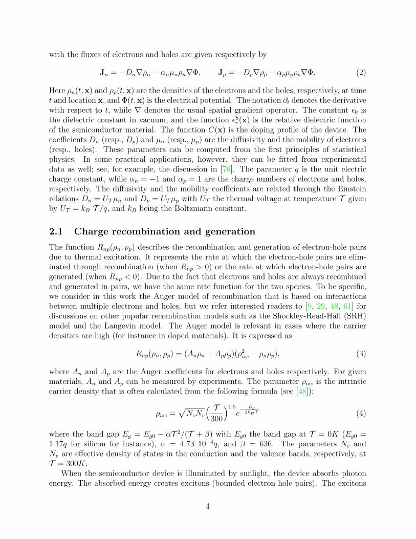
In simulations done for practical applications, it is often assumed that the densities for thereductants and oxidants in the electrolyte are extremely high, so that reductant-oxidantdynamics changes very little compared to the electron-hole dynamics in the semiconductor;see, for instance, [50, 51]. In this case, it is usually common to completely fix the electrolytesystem and only evolve the electron-hole system. This is done by treating the electrolytesystem as a Schottky contact and thus replacing the semiconductor-electrolyte interfaceconditions with Robin-type of boundary conditions such as (11); see more discussions in [50,51, 26, 42, 63]
Our previous simulations, such as those shown in Fig. 2 and Fig. 3, indicate that such asimplification indeed can be accurate as the densities of the redox pair are roughly constantinside the electrolyte. We now present two simulations where we compare the simulationsbased on the our model of the whole system with the simulations based on Schottky ap-proximation. Our simulations focus on Device II, which is significantly smaller than DeviceI. Simulations for Device I show similar behavior which we omit here to avoid repetition.
Due to the fact that the Schottky boundary condition contains no information on theparameters of the electrolyte system, it is impossible to make a direct quantitative compar-ison between the simulations. Instead, we will perform a comparison as follows. For eachconfiguration of the electrolyte system, we select the parameters Φm, χ and Eg such thattotal potential on the Schottky contact, ϕ′Stky + ϕ′app, equals the applied potential on the
counter electrode, ϕA′
app.We performed two sets of simulations on Device II. In the simulations with Schottky
18

−1 −0.8 −0.6 −0.4 −0.2 0 0.2 0.4 0.6 0.8 10
5
10Densities
−1 −0.8 −0.6 −0.4 −0.2 0 0.2 0.4 0.6 0.8 1−20
−10
0Electric field
−1 −0.8 −0.6 −0.4 −0.2 0 0.2 0.4 0.6 0.8 1−0.2
0
0.2Currents
−1 −0.8 −0.6 −0.4 −0.2 0 0.2 0.4 0.6 0.8 10
5
10Densities
−1 −0.8 −0.6 −0.4 −0.2 0 0.2 0.4 0.6 0.8 1−100
−50
0Electric field
−1 −0.8 −0.6 −0.4 −0.2 0 0.2 0.4 0.6 0.8 1−0.2
0
0.2Currents
Figure 4: Case I (b) in dark environment (γ = 0). Left column: charge densities (blacksolid for ρ′p, black dashed for ρ′n, red solid for ρ′o, and red dashed for ρ′r), electric field, andflux distributions at time t′ = 0.05. Right column: charge densities, electric field and fluxdistributions at the stationary state.
approximation, the Schottky contact locates at x′ = 0.
Case II (a). In the first set of simulations, we compare the whole system simulation withthe Schottky approximation when the bulk reductant-oxidant pair density are more than20 times higher than that of the electron-hole pair density. Precisely, the bulk densitiesfor reductant and oxidant are respectively ρ
′∞r = 30.0 and ρ
′∞o = 35.0. The results in the
semiconductor part are shown in Fig. 8. We observed that in this case, the simulations withSchottky approximation are sufficiently close to the simulations with the whole system. Thisis to say that, under such a case, replacing the electrolyte system with a Schottky contactprovides a good approximation to the original system.
Case II (b). In the second set of simulations, we compare the two simulations whenthe bulk reductant-oxidant pair density is much lower than that in Case II(a). Precisely,ρ′∞r = 2.0 and ρ
′∞o = 3.0. The results for the semiconductor part are shown in Fig. 9.While
the qualitative behavior of the two systems is similar, the quantitative results are verydifferent. We were not able to find a set of parameters in the boundary condition (11)that produced identical behavior of the semiconductor system. In this type of situations,simulation of the whole semiconductor-electrolyte system provides more accurate descriptionof the physical process in the device.
The results above show that even though one can often replace the electrolyte systemwith a Schottky contact, modeling the whole semiconductor-electrolyte system offers moreflexibilities in general. In the case when the bulk densities of the reductant and the oxidantare not extremely high compared to the densities of electrons and holes in the semiconduc-tor, replacing the electrolyte system with a Schottky contact can cause large inaccuracy inpredicted quantities.
19

−1 −0.8 −0.6 −0.4 −0.2 0 0.2 0.4 0.6 0.8 10
5
10Densities
−1 −0.8 −0.6 −0.4 −0.2 0 0.2 0.4 0.6 0.8 1−20
−10
0Electric field
−1 −0.8 −0.6 −0.4 −0.2 0 0.2 0.4 0.6 0.8 1−0.2
0
0.2Currents
−1 −0.8 −0.6 −0.4 −0.2 0 0.2 0.4 0.6 0.8 10
10
20Densities
−1 −0.8 −0.6 −0.4 −0.2 0 0.2 0.4 0.6 0.8 1−100
−50
0Electric field
−1 −0.8 −0.6 −0.4 −0.2 0 0.2 0.4 0.6 0.8 1
−0.2
0
0.2Currents
Figure 5: Case I (b) in illuminated environment (γ = 1). Left column: charge densities(black solid for ρ′p, black dashed for ρ′n, red solid for ρ′o, and red dashed for ρ′r), electric field,and flux distributions at time t′ = 0.05. Right column: charge densities, electric field, andflux distributions at the stationary state.
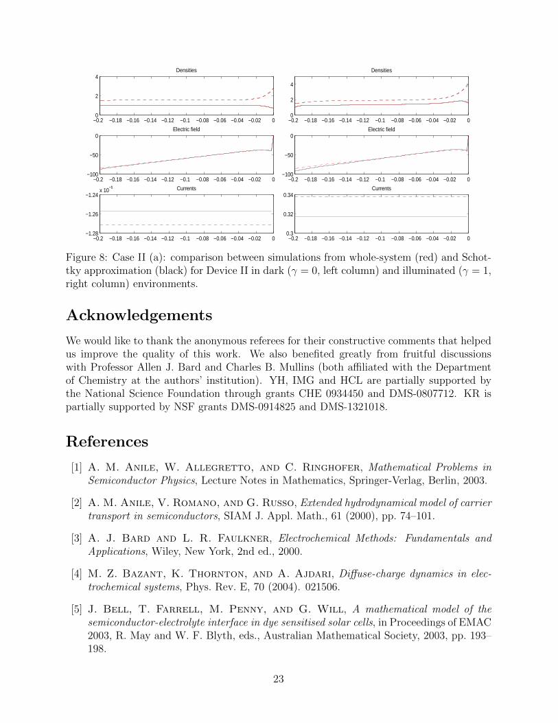
6.4 Voltage-current characteristics
In the last set of numerical simulations, we study the voltage-current, or more precisely thevoltage-flux (since all quantities are nondimensionalized), a characteristic of the semiconductor-electrolyte system. We again focus on simulations with Device II, although we observe similarresults for Device I.
Case II′ (a). We first compare simulations with forward potential bias with simulationswith reverse potential bias in a dark environment. We take a device with low bulk reductant-oxidant densities (ρ
′∞r = 4.5, ρ
′∞o = 5.0) and high relative dielectric constant in electrolyte
(εEr = 1000). Shown on the left column of Fig. 10 are electron-hole and redox pair densitiesand the corresponding electric fields for applied forward potential bias of 35.0. The sameresults for the applied reverse bias of −35.0 are presented in the right column of the samefigure. Aside from the obvious differences in the densities and electric field distributions,the fluxes through the system with forward and reverse biases are very different, as can beseen later on Fig. 12.
The simulations are repeated in Fig. 11 in the illuminated environment. It is clear fromthe plots in Fig. 10 and Fig. 11 that illumination dramatically changes the distributionof charges (and thus the electric field) inside the device as we have seen in the previoussimulations.
Case II′ (b). We now attempt to explore the whole voltage-flux (I-V) characteristics ofDevice II. To do that, we run the simulations for various different applied potentials andcompute the flux through the system under each applied potential. We plot the flux data asa function of the applied potential to obtain the I-V curve of the system. The parameters
20

−1 −0.8 −0.6 −0.4 −0.2 0 0.2 0.4 0.6 0.8 10
2
4
6Densities
−1 −0.8 −0.6 −0.4 −0.2 0 0.2 0.4 0.6 0.8 1−100
0
100Electric field
−1 −0.8 −0.6 −0.4 −0.2 0 0.2 0.4 0.6 0.8 1−0.5
0
0.5Currents
−1 −0.8 −0.6 −0.4 −0.2 0 0.2 0.4 0.6 0.8 10
2
4
6Densities
−1 −0.8 −0.6 −0.4 −0.2 0 0.2 0.4 0.6 0.8 1−100
0
100Electric field
−1 −0.8 −0.6 −0.4 −0.2 0 0.2 0.4 0.6 0.8 1−0.2
0
0.2Currents
Figure 6: Case I (c) in dark environment (γ = 0). Shown are: charge densities (blacksolid for ρ′p, black dashed for ρ′n, red solid for ρ′o, and red dashed for ρ′r), electric field,and flux distributions at time t′ = 0.05 (left); and charge densities, electric field, and fluxdistributions at the stationary state (right).
are taken as ρ′∞r = 35, ρ
′∞o = 30), and εEr = 1000 to mimic those in realistic devices.
Fig. 12 shows the I-V curve obtained in both dark (line with stars) and illuminated (solidline with circles) environments. The applied potential bias lives in the range [−58.0, 73.5].The intersections of the dash-dotted vertical lines with the x-axis (horizontal) show themaximum power voltage (Φmp, red) and open circuit voltage (Φoc, blue). The intersectionsof the dashed horizontal lines with the y-axis show the maximum power flux (Joc, red) andshort circuit flux (Jsc, blue).
7 Conclusion and remarks
We have considered in this paper the mathematical modeling of semiconductor-electrolytesystems for applications in liquid-junction solar cells. We presented a complete mathemati-cal model, a set of nonlinear partial differential equations with reactive interface conditions,for the simulation of such systems. Our model consists of a reaction-drift-diffusion-Poissonsystem that models the transport of electron-hole pairs in the semiconductor and an equiv-alent system that describes the transport of reductant-oxidant pairs in the electrolyte. Thecoupling of the two systems on the semiconductor-electrolyte interface is modeled with aset of reaction and flux transfer types of interface conditions. We presented numericalprocedures to solve both the time-dependent and stationary problems, for instance withGummel-Schwarz double iteration. Some numerical simulations for one-dimensional deviceswere presented to illustrate the behavior of these devices.
Past study on the semiconductor-electrolyte system usually completely neglected thecharge transfer processes in the electrolyte [50, 51, 26, 42, 63]. The mathematical modelsdeveloped thus only cover the semiconductor part with the interface effect modeled by a
21

−1 −0.8 −0.6 −0.4 −0.2 0 0.2 0.4 0.6 0.8 10
2
4
6Densities
−1 −0.8 −0.6 −0.4 −0.2 0 0.2 0.4 0.6 0.8 1−100
−50
0
50Electric field
−1 −0.8 −0.6 −0.4 −0.2 0 0.2 0.4 0.6 0.8 1−0.5
0
0.5Currents
−1 −0.8 −0.6 −0.4 −0.2 0 0.2 0.4 0.6 0.8 10
5
10Densities
−1 −0.8 −0.6 −0.4 −0.2 0 0.2 0.4 0.6 0.8 1−100
0
100Electric field
−1 −0.8 −0.6 −0.4 −0.2 0 0.2 0.4 0.6 0.8 1−0.2
0
0.2Currents
Figure 7: Case I (c) in illuminated environment (γ = 1). Shown are: charge densities (blacksolid for ρ′p, black dashed for ρ′n, red solid for ρ′o and red dashed for ρ′r respectively), electricfield and flux distributions at time t′ = 0.05 (left column); and charge densities, electricfield, and flux distributions at the stationary state (right column).
Robin type of boundary condition. The rationale behind this simplification is the beliefthat the density of the reductant-oxidant pairs is so high compared to the density of theelectron-hole pairs in the semiconductor such that the density of the redox pair would not beperturbed by the charge transfer process through the interface. While this might be a validapproximation in certain cases, it can certainly go wrong in other cases. For instance, it isgenerally observed that due to the strong electric field at the interface, there are dramaticchange in the density of charges (both the electron-hole and the redox pairs) near theinterface. What we have presented is, to our knowledge, the first complete mathematicalmodel for semiconductor-electrolyte solar cell systems that would allow us to accuratelystudy the charge transfer process through the interface.
There are a variety of problems related to the model that we have constructed in this workthat deserve thorough investigations. On the mathematical side, a detailed mathematicalanalysis on the well-posedness of the system is necessary. On the computational side, moredetailed numerical analysis of the model, including convergence of the Gummel-Schwarziteration, efficient high-order discretization, and fast solution techniques, has to be studied.On the application side, it is important to calibrate the model parameters with experimentaldata collected from real semiconductor-electrolyte solar cells. Once the aforementioned issuesare addressed, we can use the model to help design more efficient solar cells by, for instance,optimizing the various model parameters. We are currently investigating several of theseissues.
22
−0.2 −0.18 −0.16 −0.14 −0.12 −0.1 −0.08 −0.06 −0.04 −0.02 00
2
4Densities
−0.2 −0.18 −0.16 −0.14 −0.12 −0.1 −0.08 −0.06 −0.04 −0.02 0−100
−50
0Electric field
−0.2 −0.18 −0.16 −0.14 −0.12 −0.1 −0.08 −0.06 −0.04 −0.02 0−1.28
−1.26
−1.24x 10
−5 Currents
−0.2 −0.18 −0.16 −0.14 −0.12 −0.1 −0.08 −0.06 −0.04 −0.02 00
2
4
Densities
−0.2 −0.18 −0.16 −0.14 −0.12 −0.1 −0.08 −0.06 −0.04 −0.02 0−100
−50
0Electric field
−0.2 −0.18 −0.16 −0.14 −0.12 −0.1 −0.08 −0.06 −0.04 −0.02 00.3
0.32
0.34Currents
Figure 8: Case II (a): comparison between simulations from whole-system (red) and Schot-tky approximation (black) for Device II in dark (γ = 0, left column) and illuminated (γ = 1,right column) environments.
Acknowledgements
We would like to thank the anonymous referees for their constructive comments that helpedus improve the quality of this work. We also benefited greatly from fruitful discussionswith Professor Allen J. Bard and Charles B. Mullins (both affiliated with the Departmentof Chemistry at the authors’ institution). YH, IMG and HCL are partially supported bythe National Science Foundation through grants CHE 0934450 and DMS-0807712. KR ispartially supported by NSF grants DMS-0914825 and DMS-1321018.
References
[1] A. M. Anile, W. Allegretto, and C. Ringhofer, Mathematical Problems inSemiconductor Physics, Lecture Notes in Mathematics, Springer-Verlag, Berlin, 2003.
[2] A. M. Anile, V. Romano, and G. Russo, Extended hydrodynamical model of carriertransport in semiconductors, SIAM J. Appl. Math., 61 (2000), pp. 74–101.
[3] A. J. Bard and L. R. Faulkner, Electrochemical Methods: Fundamentals andApplications, Wiley, New York, 2nd ed., 2000.
[4] M. Z. Bazant, K. Thornton, and A. Ajdari, Diffuse-charge dynamics in elec-trochemical systems, Phys. Rev. E, 70 (2004). 021506.
[5] J. Bell, T. Farrell, M. Penny, and G. Will, A mathematical model of thesemiconductor-electrolyte interface in dye sensitised solar cells, in Proceedings of EMAC2003, R. May and W. F. Blyth, eds., Australian Mathematical Society, 2003, pp. 193–198.
23

−0.2 −0.18 −0.16 −0.14 −0.12 −0.1 −0.08 −0.06 −0.04 −0.02 00
2
4
Densities
−0.2 −0.18 −0.16 −0.14 −0.12 −0.1 −0.08 −0.06 −0.04 −0.02 0−200
−100
0Electric field
−0.2 −0.18 −0.16 −0.14 −0.12 −0.1 −0.08 −0.06 −0.04 −0.02 0−2
−1
0x 10
−6 Currents
−0.2 −0.18 −0.16 −0.14 −0.12 −0.1 −0.08 −0.06 −0.04 −0.02 00
5
10Densities
−0.2 −0.18 −0.16 −0.14 −0.12 −0.1 −0.08 −0.06 −0.04 −0.02 0−200
−100
0Electric field
−0.2 −0.18 −0.16 −0.14 −0.12 −0.1 −0.08 −0.06 −0.04 −0.02 00.4
0.6
0.8Currents
Figure 9: Case II (b): comparison between simulations from whole-system (red) and Schot-tky approximation (black) for Device II in dark (γ = 0, left column) and illuminated (γ = 1,right column) environments.
−0.2 −0.15 −0.1 −0.05 0 0.05 0.1 0.15 0.20
2
4
6Densities
−0.2 −0.15 −0.1 −0.05 0 0.05 0.1 0.15 0.2−80
−60
−40
−20
0
Electric field
−0.2 −0.15 −0.1 −0.05 0 0.05 0.1 0.15 0.20
2
4
6Densities
−0.2 −0.15 −0.1 −0.05 0 0.05 0.1 0.15 0.2
0
20
40
60
80Electric field
Figure 10: Case II′ (a) in dark (γ = 0) environment: comparison of charge densities (top)and the corresponding electric fields (bottom) in applied forward (left column) and reversed(right column) potential bias.
[6] N. Ben Abdallah, M. J. Caceres, J. A. Carrillo, and F. Vecil, A deter-ministic solver for a hybrid quantum-classical transport model in nanoMOSFETs, J.Comput. Phys., 228 (2009), pp. 6553–6571.
[7] N. Ben Abdallah and P. Degond, On a hierarchy of macroscopic models forsemiconductors, J. Math. Phys., 37 (1996), pp. 3306–3333.
[8] P. M. Biesheuvel, Y. Fu, and M. Z. Bazant, Electrochemistry and capacitivecharging of porous electrodes in asymmetric multicomponent electrolytes, Russian J.Electrochem., 48 (2012), pp. 580–592.
[9] K. F. Brennan, The Physics of Semiconductors : with Applications to OptoelectronicDevices, Cambridge University Press, New York, 1999.
24
−0.2 −0.15 −0.1 −0.05 0 0.05 0.1 0.15 0.20
5
10
15Densities
−0.2 −0.15 −0.1 −0.05 0 0.05 0.1 0.15 0.2−80
−60
−40
−20
0
Electric field
−0.2 −0.15 −0.1 −0.05 0 0.05 0.1 0.15 0.20
2
4
6
8
10Densities
−0.2 −0.15 −0.1 −0.05 0 0.05 0.1 0.15 0.2
0
20
40
60
80Electric field
Figure 11: Case II′ (a) in illuminated (γ = 1) environment: comparison of charge densities(top) and the corresponding electric fields (bottom) in applied forward (left) and reverse(right) potential bias.
−60 −40 −20 0 20 40 60 80−0.4
−0.3
−0.2
−0.1
0
0.1
0.2
0.3
Voltage [Φ*]
Curre
nt [1
0−8 q
C* l* / t* ]
illuminated
dark
Figure 12: Case II′ (b): voltage-flux (I-V) curves for an n-type semiconductor-electrolytesystem in dark (dotted line with circles) and illuminated (solid line with dots) environments.The intersections of the dash-dotted vertical lines with the x-axis show the maximum powervoltage (Φmp, red) and open circuit voltage (Φoc, blue). The intersections of the dashedhorizontal lines with the y-axis show the maximum power flux (Joc, red) and short circuitflux (Jsc, blue).
[10] M. Burger and R. Pinnau, A globally convergent Gummel map for optimal dopantprofiling, Math. Models Methods Appl. Sci., 19 (2009), pp. 769–786.
[11] C. Capellos and B. Bielski, Kinetic Systems: Mathematical Description of Chem-ical Kinetics in Solution, Wiley-Interscience, New York, 1972.
[12] J. A. Carrillo, I. Gamba, and C.-W. Shu, Computational macroscopic approx-imations to the one-dimensional relaxation-time kinetic system for semiconductors,Physica D, 146 (2000), pp. 289–306.
[13] J. A. Carrillo, I. M. Gamba, A. Majorana, and C.-W. Shu, A WENO-solverfor the transients of Boltzmann-Poisson system for semiconductor devices: Performanceand comparisons with Monte Carlo methods, J. Comput. Phys., 184 (2003), pp. 498–525.
25

[14] C. Cercignani, I. M. Gamba, and C. D. Levermore, High field approximationsto a Boltzmann-Poisson system and boundary conditions in a semiconductor, Appl.Math. Lett., 10 (1997), pp. 111–118.
[15] , A drift-collision balance asymptotic for a Boltzmann-Poisson system in boundeddomains, SIAM J. Appl. Math., 61 (2001), pp. 1932–1958.
[16] S. Chen, W. E, Y. Liu, and C.-W. Shu, A discontinuous Galerkin implementationof a domain decomposition method for kinetic-hydrodynamic coupling multiscale prob-lems in gas dynamics and device simulations, J. Comput. Phys., 225 (2007), pp. 1314–1330.
[17] Y. Cheng, I. Gamba, and K. Ren, Recovering doping profiles in semiconductordevices with the Boltzmann-Poisson model, J. Comput. Phys., 230 (2011), pp. 3391–3412.
[18] K. A. Connors, Chemical Kinetics, The Study of Reaction Rates in Solution, VCHPublishers, Weinheim, Germany, 1990.
[19] C. de Falco, M. Porro, R. Sacco, and M. Verri, Multiscale modeling andsimulation of organic solar cells, Comput. Methods Appl. Mech. Engrg., 245 (2012),pp. 102–116.
[20] P. Degond and B. Niclot, Numerical analysis of the weighted particle method ap-plied to the semiconductor Boltzmann equation, Numer. Math., 55 (1989), pp. 599–618.
[21] A. Deinega and S. John, Finite difference discretization of semiconductor drift-diffusion equations for nanowire solar cells, Comput. Phys. Commun., 183 (2012),pp. 2128–2135.
[22] J. C. deMello, Highly convergent simulations of transport dynamics in organic light-emitting diodes, J. Comput. Phys., 181 (2002), pp. 564–576.
[23] C. R. Drago and R. Pinnau, Optimal dopant profiling based on energy-transportsemiconductor models, Math. Models Methods Appl. Sci., 18 (2008), pp. 195–241.
[24] B. Eisenberg, Ionic channels: Natural nanotubes described by the drift diffusion equa-tions, Superlattices and Microstructures, 27 (2000), pp. 545–549.
[25] A. M. Fajardo and N. S. Lewis, Free-energy dependence of electron-transfer rateconstants at Si/liquid interfaces, J. Phys. Chem. B, 101 (1997), pp. 11136–11151.
[26] W. R. Fawcett, Liquids, Solutions, and Interfaces: From Classical Macroscopic De-scriptions to Modern Microscopic Details, Oxford University Press, New York, 2004.
[27] F. Filbet and S. Jin, A class of asymptotic-preserving schemes for kinetic equationsand related problems with stiff sources, J. Comput. Phys., 229 (2010), pp. 7625–7648.
26

[28] J. M. Foley, M. J. Price, J. I. Feldblyum, and S. Maldonado, Analysis of theoperation of thin nanowire photoelectrodes for solar energy conversion, Energy Environ.Sci., 5 (2012), pp. 5203–5220.
[29] J. M. Foster, J. Kirkpatrick, and G. Richardson, Asymptotic and numericalprediction of current-voltage curves for an organic bilayer solar cell under varying illu-mination and comparison to the Shockley equivalent circuit, J. Appl. Phys., 114 (2013).104501.
[30] S. Gadau and A. Jungel, A three-dimensional mixed finite-element approximationof the semiconductor energy-transport equations, SIAM J. Sci. Comput., 31 (2008),pp. 1120–1140.
[31] M. Galler, Multigroup equations for the description of the particle transport in semi-conductors, World Scientific, 2005.
[32] Y. Gao, Y. Georgievskii, and R. Marcus, On the theory of electron transfer reac-tions at semiconductor electrode/liquid interfaces, J. Phys. Chem., 112 (2000), pp. 3358–3369.
[33] Y. Gao and R. Marcus, On the theory of electron transfer reactions at semiconduc-tor electrode/liquid interfaces. II. A free electron model, J. Phys. Chem., 112 (2000),pp. 6351–6360.
[34] A. Glitzky, Analysis of electronic models for solar cells including energy resolveddefect densities, Math. Methods Appl. Sci., 34 (2011), pp. 1980–1998.
[35] T. Grasser, ed., Advanced Device Modeling and Simulation, World Scientific, 2003.
[36] M. Gratzel, Photoelectrochemical cells, Nature, 414 (2001), pp. 338–344.
[37] , Dye-sensitized solar cells, J. Photochem. Photobiol. C, 4 (2003), pp. 145–153.
[38] H. Haug and A.-P. Jauho, Quantum Kinetics in Transport and Optics of Semicon-ductors, Springer-Verlag, Berlin, 1996.
[39] B. Hille, Ionic Channels of Excitable Membranes, Sinauer Associates, Sunderland,MA., 3nd ed., 2001.
[40] T. L. Horng, T. C. Lin, C. Liu, and B. Eisenberg, PNP equations with stericeffects: A model of ion flow through channels, J Phys Chem B., 116 (2012), pp. 11422–11441.
[41] J. W. Jerome, Analysis of Charge Transport: A Mathematical Study of SemiconductorDevices, Springer-Verlag, Berlin, 1996.
[42] J. Jin, K. Walczak, M. R. Singh, C. Karp, N. S. Lewis, and C. Xiang, Anexperimental and modeling/simulation-based evaluation of the efficiency and operationalperformance characteristics of an integrated, membrane-free, neutral pH solar-drivenwater-splitting system, Energy Environ. Sci., 7 (2014), pp. 3371–3380.
27

[43] S. Jin and L. Pareschi, Discretization of the multiscale semiconductor Boltzmannequation by diffusive relaxation schemes, J. Comput. Phys., 161 (2000), pp. 312–330.
[44] A. Jungel, Transport Equations for Semiconductors, Springer, Berlin, 2009.
[45] P. V. Kamat, K. Tvrdy, D. R. Baker, and J. G. Radich, Beyond photovoltaics:Semiconductor nanoarchitectures for liquid-junction solar cells, Chem. Rev., 110 (2010),pp. 6664–6688.
[46] B. M. Kayes, H. A. Atwater, and N. S. Lewis, Comparison of the device physicsprinciples of planar and radial p-n junction nanorod solar cells, J. Appl. Phys., 97(2005). 114302.
[47] M. S. Kilic, M. Z. Bazant, and A.Ajdari, Steric effects in the dynamics ofelectrolytes at large applied voltages: II. modified Nernst-Planck equations, Phys. Rev.E, 75 (2007). 021503.
[48] R. Kircher and W. Bergner, Three-Dimensional Simulation of SemiconductorDevices, Berkhauser Verlag, Basel, 1991.
[49] A. A. Kulikovsky, A more accurate Scharfetter-Gummel algorithm of electron trans-port for semiconductor and gas discharge simulation, J. Comput. Phys., 119 (1995),pp. 149–155.
[50] D. Laser and A. J. Bard, Semiconductor electrodes: VII digital simulation of chargeinjection and the establishment of the space charge region in the absence of surfacestates, J. Electrochem. Soc., 123 (1976), pp. 1828–1832.
[51] , Semiconductor electrodes: VIII digital simulation of open-circuit photopotentials,J. Electrochem. Soc., 123 (1976), pp. 1833–1837.
[52] N. S. Lewis, Mechanistic studies of light-induced charge separation at semiconduc-tor/liquid interfaces, Acc. Chem. Res., 23 (1990), pp. 176–183.
[53] , Progress in understanding electron-transfer reactions at semiconductor/liquid in-terfaces, J. Phys. Chem. B, 102 (1998), pp. 4843–4855.
[54] J. Li, Y. Chen, and Y. Liu, Mathematical simulation of metamaterial solar cells,Adv. Appl. Math. Mech., 3 (2011), pp. 702–715.
[55] P.-L. Lions, On the Schwarz alternating method. I., in Domain Decomposition Meth-ods, SIAM, Philadelphia, 1988, pp. 1–42.
[56] , On the Schwarz alternating method. II. Stochastic interpretation and order prop-erties., in Domain Decomposition Methods, SIAM, Philadelphia, 1989, pp. 47–70.
[57] W. Liu, One-dimensional steady-state Poisson-Nernst-Planck systems for ion channelswith multiple ion species, J. Diff. Eqn., 246 (2009), pp. 428–451.
28

[58] B. Lu and Y. C. Zhou, Poisson-Nernst-Planck equations for simulating biomoleculardiffusion-reaction processes II: Size effects on ionic distributions and diffusion-reactionrates, Biophysical Journal, 100 (2011), pp. 2475–2485.
[59] S. Mafe, J. Pellicer, and V. M. Aguilella, A numerical approach to ionictransport through charged membranes, J. Comput. Phys., 75 (1988), pp. 1–14.
[60] A. Majorana and R. Pidatella, A finite difference scheme solving the Boltzmann-Poisson system for semiconductor devices, J. Comput. Phys., 174 (2001), pp. 649–668.
[61] P. A. Markowich, C. A. Ringhofer, and C. Schmeiser, Semiconductor Equa-tions, Springer, New York, 1990.
[62] S. R. Mathur and J. Y. Murthy, A multigrid method for the Poisson-Nernst-Planck equations, Int. J. Heat Mass Transfer, 52 (2009), pp. 4031–4039.
[63] R. Memming, Semiconductor Electrochemistry, Wiley-VCH, New York, 2001.
[64] S. Micheletti, A. Quarteroni, and R. Sacco, Current-voltage characteristicssimulation of semiconductor devices using domain decomposition, J. Comput. Phys.,119 (1995), pp. 46–61.
[65] J. Nelson, The Physics of Solar Cells, Imperial College Press, London, 2003.
[66] J. Newman and K. E. Thomas-Alyea, Electrochemical Systems, Wiley-Interscience, New York, 3rd ed., 2004.
[67] B. Niclot, P. Degond, and F. Poupaud, Deterministic particle simulations of theBoltzmann transport equation of semiconductors, J. Comput. Phys., 78 (1988), pp. 313–349.
[68] A. J. Nozik and R. Memming, Physical chemistry of semiconductor-liquid interfaces,J. Phys. Chem., 100 (1996), pp. 13061–13078.
[69] J. H. Park and J. W. Jerome, Qualitative properties of steady-state Poisson–Nernst–Planck systems: Mathematical study, SIAM J. Appl. Math., 57 (1997), pp. 609–630.
[70] M. Penny, T. Farrell, and C. Please, A mathematical model for interfacialcharge transfer at the semiconductor-dye-electrolyte interface of a dye-sensitised solarcell, Solar Energy Materials and Solar Cells, 92 (2008), pp. 11–23.
[71] M. A. Penny, T. W. Farrell, G. D. Will, and J. M. Bell, Modelling interfacialcharge transfer in dye-sensitised solar cells, J. Photochem. Photobiol. A, 164 (2004),pp. 41–46.
[72] K. E. Pomykal and N. S. Lewis, Measurement of interfacial charge-transfer rateconstants at n-type InP/CHOH junctions, J. Phys. Chem. B, 101 (1997), pp. 2476–2484.
29
[73] G. Richardson, C. Please, J. Foster, and J. Kirkpatrick, Asymptotic solutionof a model for bilayer organic diodes and solar cells, SIAM J. Appl. Math., 72 (2012),pp. 1792–1817.
[74] C. A. Ringhofer, Computational methods for semiclassical and quantum transportin semiconductor devices, Acta Numer., 6 (1997), pp. 485–521.
[75] A. Rossani, A new derivation of the drift-diffusion equations for electrons andphonons, Physica A, 390 (2011), pp. 223–230.
[76] A. Schenk, Advanced Physical Models for Silicon Device Simulation, Springer, Wien,1998.
[77] D. Schroeder, Modelling of Interface Carrier Transport for Device Simulation,Springer-Verlag, Wien, 1994.
[78] Z. Schuss, B. Nadler, and R. S. Eisenberg, Derivation of PNP equations in bathand channel from a molecular model, Phys. Rev. E, 64 (2001). 036116.
[79] S. Selberherr, Analysis and Simulation of Semiconductor Devices, Springer, Vienna,1984.
[80] N. Seoane, A. J. Garcıa-Loureiro, K. Kalna, and A. Asenov, Impact ofintrinsic parameter fluctuations on the performance of HEMTs studied with a 3d paralleldrift-diffusion simulator, Solid-State Electronics, 51 (2007), pp. 481–488.
[81] A. Singer and J. Norbury, A Poisson-Nernst-Planck model for biological ionchannels-an asymptotic analysis in a three-dimensional narrow fun, SIAM J. Appl.Math., 70 (2009), pp. 949–968.
[82] D. Singh, X. Guo, J. Y. Murthy, A. Alexeenko, and T. Fisher, Modelingof subcontinuum thermal transport across semiconductor-gas interfaces, J. Appl. Phys.,106 (2009). 024314.
[83] H. Steinruck, A bifurcation analysis of the one-dimensional steady-state semiconduc-tor device equations, SIAM J. Appl. Math., 49 (1989), pp. 1102–1121.
[84] M. J. Ward, L. G. Reyna, and F. M. Odeh, Multiple steady-state solutions in amultijunction semiconductor device, SIAM J. Appl. Math., 51 (1991), pp. 90–123.
[85] P. Y. Yu and M. Cardona, Fundamentals of Semiconductors: Physics and MaterialsProperties, Springer, Berlin, 3rd ed., 2003.
[86] S. Zhao, J. Ovadia, X. Liu, Y.-T. Zhang, and Q. Nie, Operator splitting implicitintegration factor methods for stiff reaction-diffusion-advection systems, J. Comput.Phys., 230 (2011), pp. 5996–6009.
30