Embed Size (px)
Citation preview

Op Amp compensation
The design process involves two distinct activities:
• Architecture Design – Find an architecture already available and
adapt it to present requirements – Create a new architecture that can meet
requirements • Component Design
– Determine transistor sizes – Determine biasing voltages/currents – Design compensation network

All op amps used as feedback amplifier:
If not compensated well, closed-loop can be oscillatory or unstable. damping ratio ζ ≈ phase margin PM / 100
Value of ζ: 1 0.7 0.6 0.5 0.4 0.3 Overshoot: 0 5% 9.6% 16% 25% 37% PM in deg: 67 61 53 44 35 PM+Mp: 72 71 69 69 72 PM+Mp=70


UGF: frequency at which gain = 1 or 0 dB PM: phase margin = how much the phase is above critical (-180o) at UGF
Closed-loop is unstable if PM < 0
PM
UGF This is the loop-return gain when used in closed-loop. Only in buffer connection this is equal to O.L. gain.

z

UGF
p1 p2

PM
GM
p1 p2 z1
UGF

Types of Compensation • Miller - Use of a capacitor feeding back around a
high-gain, inverting stage. – Miller capacitor only – Miller capacitor with an unity-gain buffer to block the
forward path through the compensation capacitor. Can eliminate the RHP zero.
– Miller with a nulling resistor. Similar to Miller but with an added series resistance to gain control over the RHP zero.
• Self compensating - Load capacitor compensates the op amp (later).
• Feedforward - Bypassing a positive gain amplifier resulting in phase lead. Gain can be less than unity.

VsA2A1
Cc
VoutA
Two stage Miller compensation
v1 v2= AVv1
i
i = (v1-v2)/Zf = v1(1-AV)/Zf = v1/{Zf /(1-AV)} = - v2(1-1/AV)/Zf = - v2/{Zf /(1-1/AV)}
i= v1/Z1
i= -v2/Z2
v1 v2 Miller Effect

Vs+A2-A1
C1
A-A2
C2
B Vout
Vs+A2-A1
C1
A-A3
C2
B Vout
Vs-A2-A1
C1
A+A3
C2
B Vout
-AF1
Vs+A2-A1
C1
A-A3
C2
B Vout
-AF1
+AF2
(a) (b)
(c) (d)
(a) Nested Miller Compensation (NMC), (b) Reverse Nested Miller Compensation (RNMC), (c) Multipath Nested Miller Compensation (MNMC), (d) Nested Gm-Cc Compensation (NGCC)

Vs+A2-A1
A-A3
Cm
B Vout
+gma
-gmf
Ca
HGB
HSB
Vs+A2-A1
A-A3
Cm
B Vout
gmf
Ca
(a) (b)
(a) Active feedback frequency compensation (AFFC), (b) Transconductance with capacitance feedback
frequency compensation (TCFC)
Single ended and differential have very similar Compensation needs
Vi+
Vo1
VBP
VBN
Vo
I2
Vi-
I1
Vi
Vo1
VBP
VBN
Vo
I2
I1
Not quite

VBP
Vi+ Vi-
VBN Vb1
CC CC
Vo+
Vi
Vo1
VBP
Vb1
Vo Vo-

VBP
Vi+ Vi-
VBN
Vb1
CC CC
Vo+ Vi
Vo1
VBP
Vb1
Vo Vo-
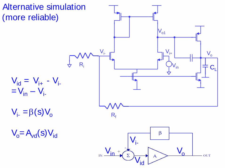
If the first stage is cascoded, the analysis stays similar
VBPc
VBNc
Composite MOST with very large ro

IN- IN+
VDD
CC CC
Vo+ Vo-
Folded cascode same thing, except gm is from a different pair

Vi
Vo1
VBP
Vb1
Vo
Generic representative:

Vi- has two components: When Vin=0, When Vo=0
What about β?
Vi+
Vo1
Vo Vi- Vin
CL
Rf
Ri
1
1
1 ||
1 ||
fgs
in
in fgs
RsC
VR R
sC+
1
1
1 ||( )1 ||
ings
o
f ings
RsC
VR R
sC
−+
Av(s) +
-
Vin(s)
β(s)
Gin(s) -Vo
Vi-

1 1
1 1
1
1 1|| ||
1 1 ( )|| ||
1
11
( )Note
In the frequency range when the op amp gain is very large,
0. This lea
ds to:( )
f ings gs o
in oo
in f f ings gs
f fo
fin in inin gs
io
o
o
in
R RsC sC VV V
A sR R R RsC sC
R RVRV R RR C sR
s
VVA s
A
−
−= ≈
−+ =
+ +
= − ≈ −+ +
+
1that this actually depends on , , and .o f in gsA R R C

Vi+
Vo1
Vo Vi-
CL
Rf
Ri
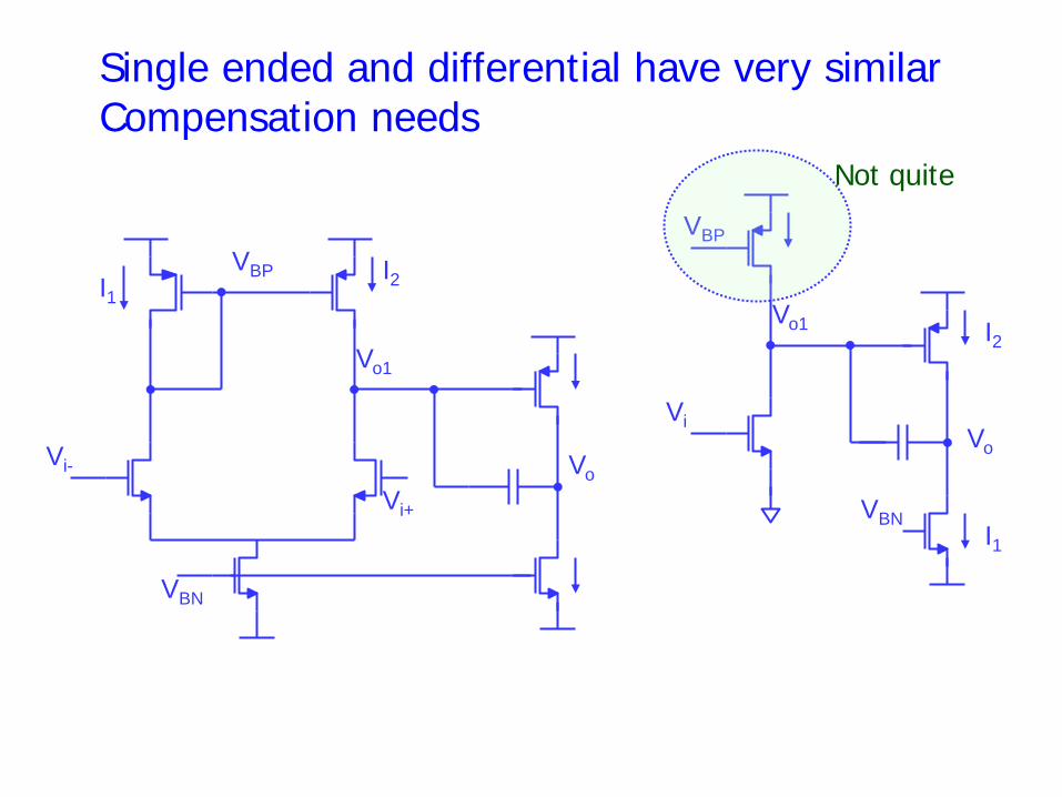
Open loop simulation incorporating feedback loading
VoQ = Vicm
V’o
Obtain freq resp from Vid to V’o
Vi+
Vo1
Vo Vi-
Vin CL
Rf
Ri
Alternative simulation (more reliable)
Vid = Vi+ - Vi- =Vin – Vi- Vi- =β(s)Vo Vo=Avd(s)Vid Vi-
Vin Vid
Vo
VBP
Vi+ Vi-
VBN
Vb1
CC CC
Vo+ Vo-
VBPc
VBNc Rf
Ri
Ri
V’o

VBP
Vi+ Vi-
VBN
Vb1
CC CC
Vo+
VBPc
VBNc
Ri
Ri
Vo-

DC gain of first stage: AV1 = -gm1/(gds2+gds4)= -gm1/(I4(λ2+ λ4)) = -gm1ro1
DC gain of second stage: AV2 = -gm6/(gds6+gds7)=- gm6/(I6(λ6+ λ7)) = -gm6ro
Total DC gain: AV =
gm1gm6 (gds2+gds4)(gds6+gds7)
GBW = gm1/CC
AV = gm1gm6ro1ro

Zf = 1/s(CC+Cgd6) ≈ 1/sCC
When considering p1 (low freq), can ignore CL (including parasitics at vo):
Therefore, AV6 = -gm6/(gds6+gds7)
Z1eq = 1/sCC(1+ gm6/(gds6+gds7)) C1eq=CC(1+ gm6/(gds6+gds7))≈CCgm6/(gds6+gds7)
-p1 = ω1 ≈ (gds2+gds4)/(C1+C1eq) ≈ (gds2+gds4)/(C1+CCgm6/(gds6+gds7)) ≈ (gds2+gds4)(gds6+gds7)/(CCgm6) -p1 = ω1 ≈ 1/(ro1CC|AV6|)
Note: ω1 decreases with increasing CC

At frequencies much higher than ω1, gds2 and gds4 can be viewed as open.
Μ7
C1
CC
CL
vo
Total go at vo:
gds6+gds7+gm6 CC
CC+C1 Total C at vo:
CL+ C1CC CC+C1
-p2=ω2= CCgm6+(C1+CC)(gds6+gds7)
CL(C1+CC)+CCC1
Μ6

Note that when CC=0, ω2 = gds6+gds7 CL
As CC is increased, ω2 increases also.
However, when CC is large, ω2 does not increase as much with CC. ω2 has a upper limit given by: gm6+gds6+gds7
CL+C1
Hence, once CC is large, its main effect is to lower ω1, and hence lower GBW.
≈ gm6 CL+C1
When CC=C1, ω2 ≈ (½gm6+gds6+gds7)/(CL+½C1) ≈ gm6/(2CL+C1)
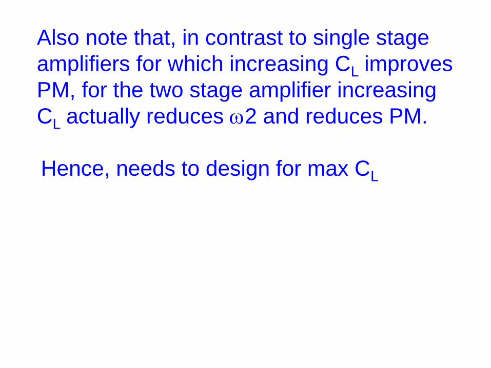
Also note that, in contrast to single stage amplifiers for which increasing CL improves PM, for the two stage amplifier increasing CL actually reduces ω2 and reduces PM.
Hence, needs to design for max CL

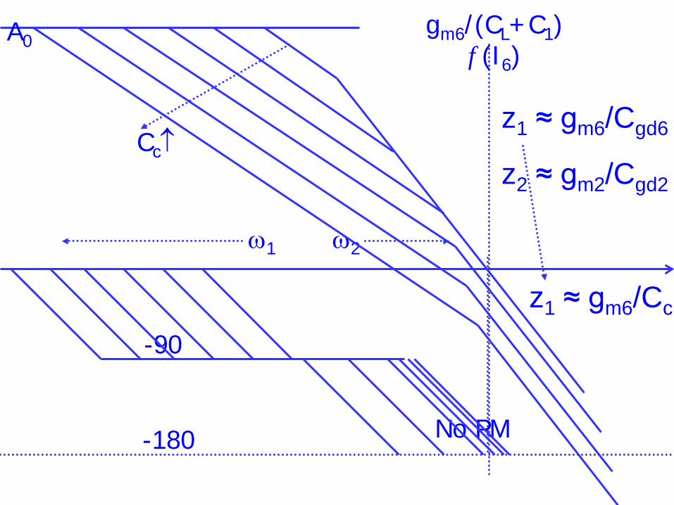
There are two RHP zeros:
z1 due to CC and M6
z1 = gm6/(CC+Cgd6) ≈ gm6/CC
z2 due to Cgd2 and M2 z2 = gm2/Cgd2 >> z1
z1 significantly affects achievable GBW.

gm6/(CL+C1) f (I6)
z1 ≈ gm6/Cgd6
A0
ω2
-90
-180
ω1 z2 ≈ gm2/Cgd2
No PM
gm6/(CL+C1) f (I6)
z1 ≈ gm6/Cgd6
A0
ω2
-90
-180
ω1
z2 ≈ gm2/Cgd2
No PM
z1 ≈ gm6/Cc
Cc↑

gm6/(CL+C1) f (I6)
z1 ≈ gm6/CC
A0
ω2
-90
-180 PM
ω1
gm1/CC

It is easy to see: PM ≈ 90o – tan-1(UGF/ω2) – tan-1(UGF/z1) To have sufficient PM, need UGF < ω2
and UGF << z1 In such case, UGF ≈ GB ≈ gm1/CC = z1 * gm1/gm6.
PM ≈ 90o – tan-1(GB/ω2) – tan-1(GB/z1)
Hence, need: GB < ω2 GB << z1
PM requirement decides how much lower:

6
,6 6 1 6
66
6 ,1
6 6,
1 max
For a given current ,
2 ,
2( )
This reaches maximum when :
1 12 2
This is the value for |
oxm L L dbp dbn gs L ox
ox
m
L L ox
L ox
m
L L
I
C Wg I C C C C C C C C WLL
C W Ig Lf IC C C C WL
C C WL
g I SRC C L C L
p
µ
µ
µ µ
= + >≈ + + + ≈ +
= ≈+ +
=
= = +
2 | when = .cC ∞

,1 16 1
, ,1 1 6
1
6
6,
1
Since
90 tan (1 ) / tan
To achiev about 50 PM, we need:
0.1
1 12 3
m mL
L L m
m
m
m
L
g gCPM GBC C C C g
gg
gGBC C
− − = ° − + − + +
°
≤
≤ +
61 1 12 3 2
Therefore, to increase GB, use NMOS 2nd stage input, large 2nd stage current, and small L.
L
IL C
µ
<

Possible design steps for max GB • For a given CL and Itot • Assume a current share ratio θ, i.e.
– I6+I5 = Itot, I5 = θI6 , I1 = I2 = I5/2 • Size W6, L6 to achieve max gm6/(CL+Cgs6)
which is > ω2 – C1 ∝ W6*L6, gm6 ∝ (W6/L6)0.5
• Size W1, L1 so that gm1 ≈ 0.1gm6 – this make z1 ≈ 10*GB
• Select CC to achieve required PM – by making gm1/CC < 0.5 ω2
• Check slew rate: SR = I5/CC • Size M5, M7, M3/4 for current ratio, ICMR, etc

Comment • If we run the same total current Itot through
a single stage common source amplifier made of M6 and M7 – Single pole go/CL – Gain gm6/go – Single stage amp GB = gm6/CL >gm6/(CL+C1) > ω2 > gm1/CC = GB of two stage amp
• Two stage amp achieves higher gain but speed is much slower!
• Can the single stage speed be recovered?

Other considerations • Output slew rate: SR = I5/CC
• Output swing range (saturation operation): VSS+Vdssat7 to VDD – Vdssat6
• Min ICM: VSS + Vdssat5 + VTN + Von1 • Max ICM: VDD - |VTP| - Von3 + VTN • Mirror node approx. pole/zero cancellation
– Closed-loop pole stuck near by – Can cause slow settling if pole freq is too low

When vin is short, the D1 node sees a capacitance CM and a conductance of gm3 through the diode con. So: pm = -gm3/CM
When vin is float and vo=0. gm4 generate a current in id4=id2=id1. So the total conductance at D1 is gm3 + gm4. So: zm = -(gm3+gm4)/CM =2*pm
If |pm| << GB, one closed-loop pole stuck nearby, causing slow settling!

Eliminating RHP Zero at gm6/CC
vg= RZCCdvCC/dt +vcc
icc = vg gm6 = CCdvCC/dt
(gm6RZ-1)CCdvCC/dt + gm6vcc=0
Vi
Vo1
VBP
Vb1
Vo
For zero from Vo1 to Vo, Set Vo = 0, float Vo1.
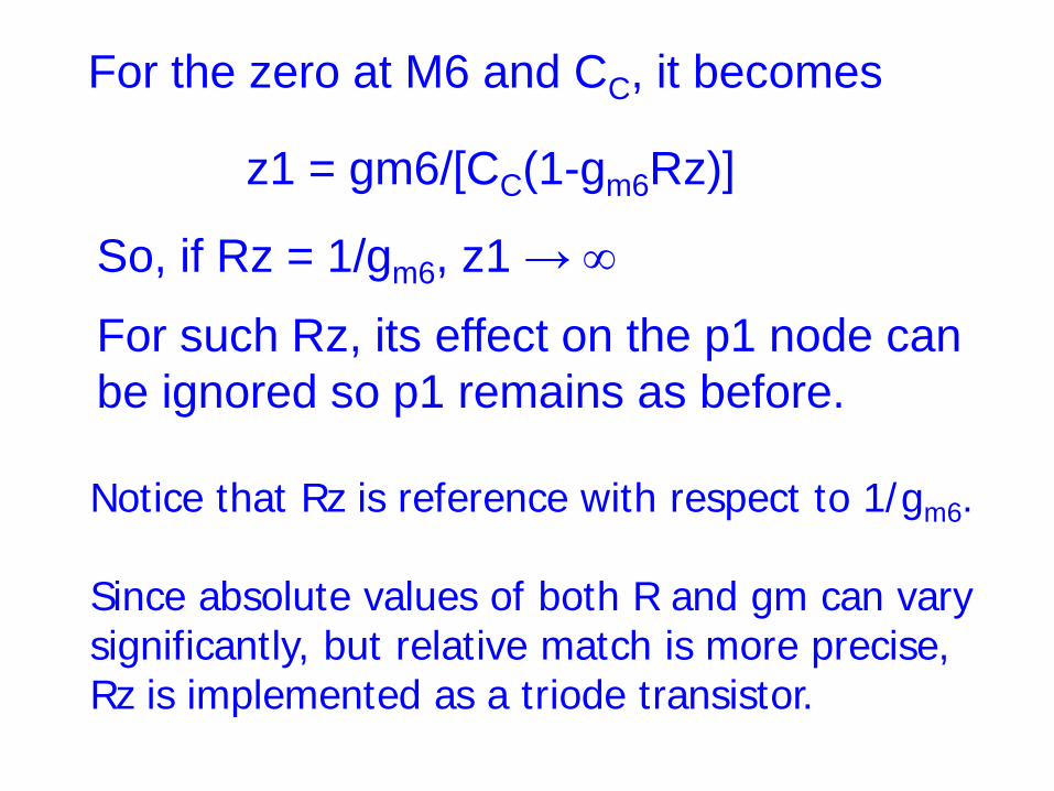
For the zero at M6 and CC, it becomes
z1 = gm6/[CC(1-gm6Rz)]
So, if Rz = 1/gm6, z1 → ∞
For such Rz, its effect on the p1 node can be ignored so p1 remains as before.
Notice that Rz is reference with respect to 1/gm6. Since absolute values of both R and gm can vary significantly, but relative match is more precise, Rz is implemented as a triode transistor.
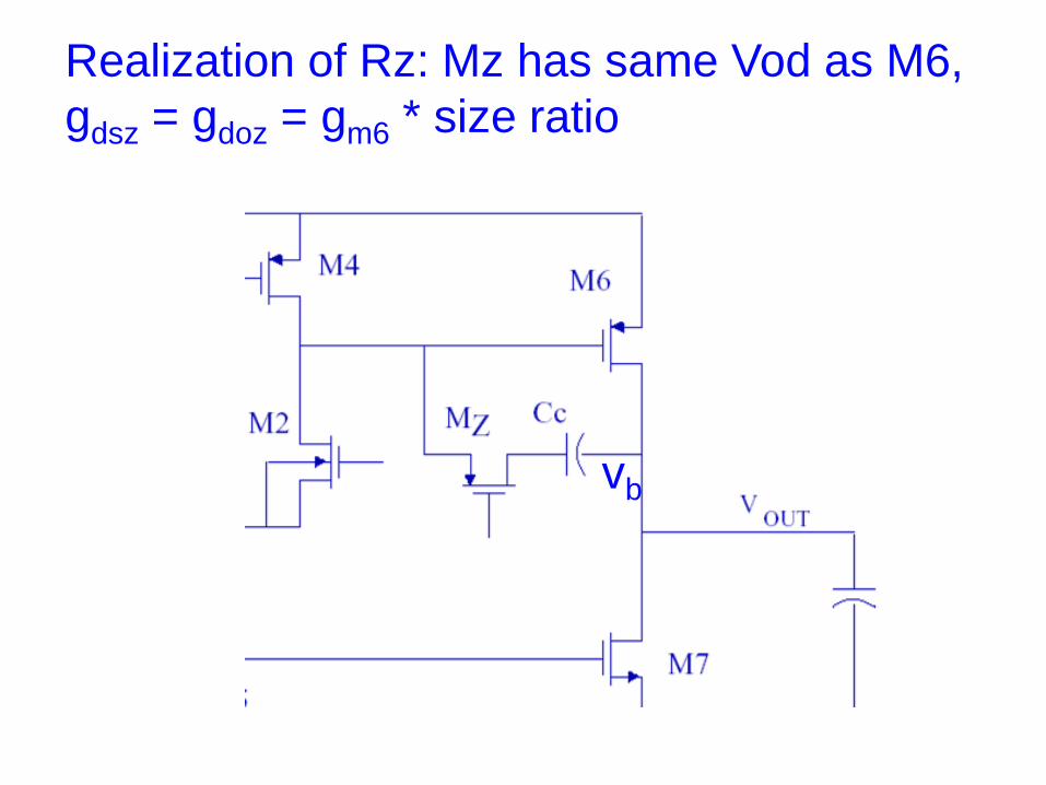
Realization of Rz: Mz has same Vod as M6, gdsz = gdoz = gm6 * size ratio
vb

Μ8
Μ9
VDD
M6, M8, M9 have same W and L, but their multiplier ratio = current ratio

Another choice of Rz, as in our book, is to make z1 cancel p2:
z1=gm6/CC(1-gm6Rz) ≈ - gm6/(CL+C1)
Rz = gm6CC
CC+CL+C1
= gm6
1 (1+ ) CC
CL+C1
Or: gdsz *( (1+ ) = gm6 CC
CL+C1

Let ID8 = αID6, size M6 and M8 so that VSG6 = VSG8
Then VSGz=VSG9 Assume Mz in triode
gdsz = βz(VSGz – |VT| - VSDz) ≈ βz(VSGz – |VT|) = βz((VSG9 – |VT|) = βz(VSG8 – |VT|) = βz(VSG6 – |VT|) = (βz/β6)gm6 = (mz/m6) gm6
Hence need: mz/m6 =CC/(CC+CL+C1)

gm6/(CL+C1) f (I6)
-z1 ≈
A0
ω2
-90
-180 PM
ω1
gm1/CC

• With the same CC as before – Z1 cancels p2 – P1 not affected much – Phase margin drop due to p2 and z1 nearly
removed – Overall phase margin greatly improved – Effects of other poles and zero become more
important
• Can we reduce CC and improve GB?

Vo1
Vb1
Vo
M6
M7
Cc Rz
'6 01 6 01
1 1 6 1 0
6
1 0 01 1
1 6
' 1 60
1 1 1 1
( ) ( )( ) 01
( )( ) 0
KCL:
1
1
1
cL o o gd o m
z c
co gd o
z c
cgd
z c co
c z c cgd
z c
c m cL o
z c c z c c
sCsC g v sC v v g vsR C
sCsC v sC v vsR CsCsC
sR C Cv v vsC sR C C C CsC sCsR C
sC C g CsC v v vsR C C C C sR C C C C
+ + + − + = + + + − ≈ +
++
= ≈+ ++ +
+
+ ++ + + + 0
'1 1 1 6
2 ' ' '1 1 1 6
62 ' '
1 1' ' '
1 1 1'
1
0
( ) 0
( ) 0
If Rz small:
1 / /
L z c c c m c
L z c L L c c m c
m c
L L c c
L L c c c c Lz
L z c z c
sC sR C C C C sC C g Cs C R C C s C C C C C C g C
g CpC C C C C C
C C C C C C C C C CpC R C C R C
≈
+ + + + =
+ + + + =
− ≈+ +
+ + + +− ≈ ≈

'6 01 6 01
6 01 6 01
26 6 6 6
61
6 6
6 62
Set = 0 in:
( ) ( )( ) 01
We get:
( ) 01
( ( ) 0
When Rz small:
( )
( )
o
cL o o gd o m
z c
cgd m
z c
z c gd gd c m z c m
m
m z c gd c
m z c gd c
z c
vsCsC g v sC v v g v
sR C
sCsC v g vsR C
s R C C s C C sg R C g
gzg R C C Cg R C C C
zR C
+ + + − + =+
− + + =+
− + + + + =
− =− +
− +− =
6
6When >1, both zeros are in left half plane.gd
m z
Cg R

6 6 62 ' ' ' '
1 1 1
' ' '1 1 1
'1 1
6 61
6 6 6
''
6 6
2
1 1 11
( ) ( 1)
When z1 is set to cancel p2,
( 1) , 1
1
1
m c m m
L L c c L L
L L c c c Lz
L z c z z
m m
m z c gd c m z c
Lm z c L m z
c
z
g C g gpC C C C C C C C C
C C C C C C C C CpC R C C R R C
g gzg R C C C g R C
Cg R C C g RC
pp
− ≈ ≈< ≈<+ + +
+ ++ +
− ≈ = >≈
− = ≈− + −
− ≈ ≈ +
>+
'
'1
L
L
c
CC CC
This ratio needs to be sufficiently large for the p/z formula to be approximately right.
When C1 large and Cc small, pz can become lower.

gm6/CL
z1 ≈ p2
A0
ω2
-90
-180
ω1
z2 ≈ gm2/Cgd2
Operate not on this but on this or this z4 ≈ gm6/Cgd6
pz=-1/RZC1
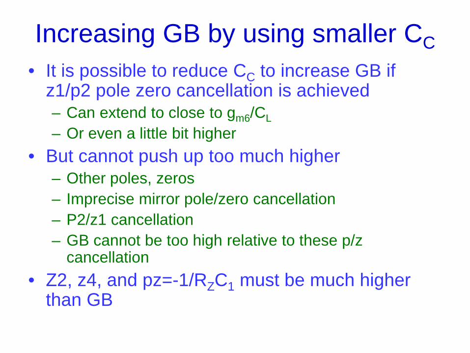
Increasing GB by using smaller CC • It is possible to reduce CC to increase GB if
z1/p2 pole zero cancellation is achieved – Can extend to close to gm6/CL – Or even a little bit higher
• But cannot push up too much higher – Other poles, zeros – Imprecise mirror pole/zero cancellation – P2/z1 cancellation – GB cannot be too high relative to these p/z
cancellation • Z2, z4, and pz=-1/RZC1 must be much higher
than GB

Possible design steps for max GB • For a given CL and Itot • Assume a current share ratio θ, i.e.
– I6+I5 = Itot, I5 = θI6 , I1 = I2 = I5/2 • Size W6, L6 to achieve max single stage GB1 =
gm6/(CL+Co-para) – A good trade off is to size W6 so that Cgs6 ≈ C1 ≈ CL/2 – If L_overlap ≈ 10% L6, this makes z4=gm6/Cgd6 ≈ 20*GB1
• Choose GB = αGB1, e.g. 0.5GB1 • Choose CC to make p2≈GB, e.g. Cc=CL/2, p2≈GB/1.25 • Size W1, L1 and adjust θ so that gm1/CC ≈ GB
– Make z2=gm2/Cgd2 >> GB, i.e. Cgd2 << Cgs2<<Cc • Size Mz so that z1 cancels p2 • Make sure PM at f=GB is sufficient • Size other transistors so that para |p| > GB*(10~20) • Check slew rate, and size other transistors for ICMR,
OSR, etc

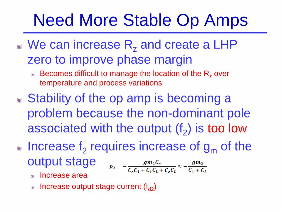
Need More Stable Op Amps We can increase Rz and create a LHP zero to improve phase margin
Becomes difficult to manage the location of the Rz over temperature and process variations
Stability of the op amp is becoming a problem because the non-dominant pole associated with the output (f2) is too low Increase f2 requires increase of gm of the output stage
Increase area Increase output stage current (Id2)

Need a more practical way to Compensate Avoid using Miller Compensation
Avoid connecting a compensation capacitor between two high impedance nodes ! Literature has many examples illustrating how to avoid miller connections for high speed
This research develops Indirect Feedback Compensation A more practical way to compensate Feedback compensation current indirectly using
Common Gate Amplifier Cascoded Structures
Improved PSRR Smaller Die Area (Compensation capacitor reduced 4~10 times) Much Faster ..!
VsA2A1 Buffer
Cc
Differential Amplifier Gain Stage Output Buffer
Vout
iccRi
A
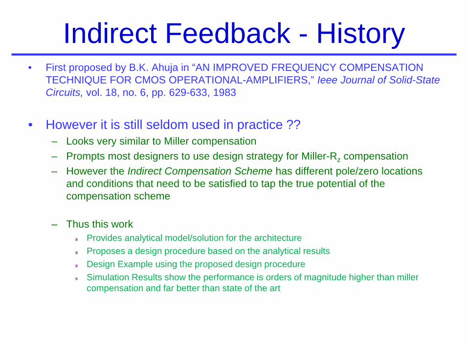
Indirect Feedback - History • First proposed by B.K. Ahuja in “AN IMPROVED FREQUENCY COMPENSATION
TECHNIQUE FOR CMOS OPERATIONAL-AMPLIFIERS,” Ieee Journal of Solid-State Circuits, vol. 18, no. 6, pp. 629-633, 1983
• However it is still seldom used in practice ?? – Looks very similar to Miller compensation – Prompts most designers to use design strategy for Miller-Rz compensation – However the Indirect Compensation Scheme has different pole/zero locations
and conditions that need to be satisfied to tap the true potential of the compensation scheme
– Thus this work Provides analytical model/solution for the architecture Proposes a design procedure based on the analytical results Design Example using the proposed design procedure Simulation Results show the performance is orders of magnitude higher than miller compensation and far better than state of the art

Indirect Feedback Frequency Compensation
Improvements due to a simple change
The compensation current is indirectly fedback from low impedance node VA to V1 The RHP pole zero can be eliminated as the feedforward current is blocked by the common gate amplifier Node V1 is now not loaded by the compensation capacitor (as previously) and thus results in a much faster second stage and increased unity gain frequency
AND MUCH MORE ………
M1 M2
M3 M4
M5
M6c
VDD
VSS
Cc
Vin- Vin+
M9
ic
VA
V1
Mb3M7
Mb1
Isupply
Mb2
Mb4
Mb5 Mb6
Vout
Vbb
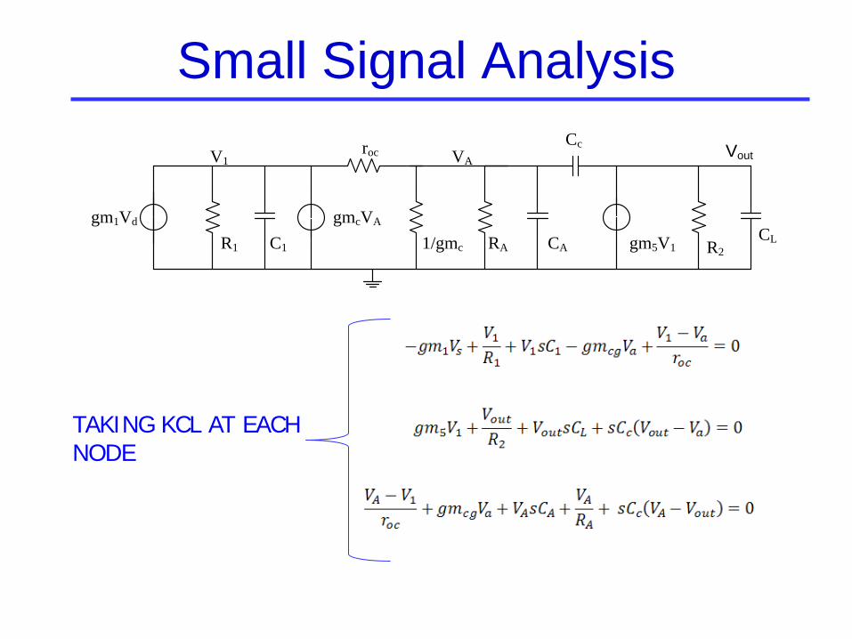
Small Signal Analysis Cc
gm1Vd
R1 C1
V1 VA
gmcVA
roc
1/gmc RA CA gm5V1 R2CL
Vout
TAKING KCL AT EACH NODE
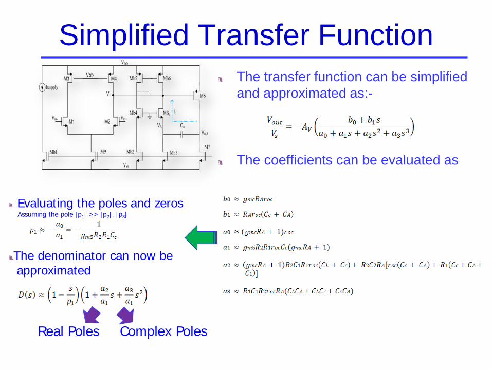
Simplified Transfer Function The transfer function can be simplified and approximated as:-
The coefficients can be evaluated as
Evaluating the poles and zeros Assuming the pole |p1| >> |p2|, |p3|
The denominator can now be
approximated
Real Poles Complex Poles

The third order transfer function as 3 poles and 1 zero Dominant Pole location Non-dominant Real Poles location
Condition For Real Poles
LHP Zero Location
bserving the Pole/Zero Locations
Remains at the same location
Large gmc ?
Improves Phase Margin

Analytical Results Summary Pole / Zero Location
Real Poles Condition
Quick Facts Pole p2 moved to much higher frequency Can use much smaller gm5 Less Power LHP zero improves the phase margin Much faster op-amp with lower power and
CC Will EXPLORE more ….
Extended by a factor >1

M1 M2
M3 M4
M5
VDD
VSS
Cc
Vin- Vin+
M9
ic
V1
M7Mb1
Isupply
Mc1 Mc2
Vbb
A
if
Vout
Vcc
Alternative Implementations of Indirect Feedback
The common gate amplifier is embedded in the cascode action Similar to the common gate amplifier analyzed in the previous section, the LHP zero and the three poles are given by Equations provided previously Reduction in Power at cost of Flexibility choosing the transconductance of gmc
M1 M2
M3 M4
M5
VDD
VSS
Cc
Vin- Vin+
M9
ic
V1
M7Mb1
Isupply
Mc1 Mc2
Vbb
A
Vout
Vcc
Similar to cascoded PMOS loads
However additional RHP zero located at:
RHP zero High Frequency

Summarizing the Advantages of Indirect Feedback
Pole splitting can be achieved with a much smaller compensation capacitor (Cc) Faster Op Amp Much Smaller Area Lower Value of second stage transconductance (gm5) value required Lower Power and Less Total Current Required Improved PSRR
Analytically the reason the non-dominant pole shifted to a higher frequency is because the compensation capacitor now does not load the first stage output.

Pre - Design Procedure Guidelines
To quantify how good of a job our transistor does, we can therefore define the following “figure of merits (FOM) Tranconductor Efficiency
Transit Frequency
Good Region For AMI 0.5CN VEB ≈ 0.1-0.2 V
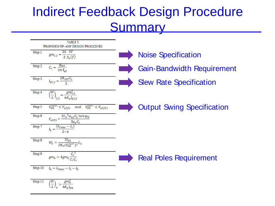
Indirect Feedback Design Procedure Summary
Noise Specification
Slew Rate Specification
Output Swing Specification
Gain-Bandwidth Requirement
Real Poles Requirement

Class A Output Stage Design Bad Output Stage Design
Not Controlling current in the output stage leads to:
Bad input-referred offset Potential for large power dissipation Not controlling output stage gm (and thus stability)
Class A output stages also suffer from poor slew rate
M1 M2
M3 M4
M5
M6c
VDD
VSS
Cc
Vin- Vin+
M9
ic
VA
V1
Mb3M7
Mb1
Isupply
Mb2
Mb4
Mb5 Mb6
Vout
Vbb
M1 M2
M3 M4
M5
VDD
Cc
V1
Mc1 Mc2Vbb
Vout
SR = inf
CLM1 M2
M3 M4
M5
VDD
Cc
V1
Mc1 Mc2Vbb
Vout
Iss2CL
SR =
CL

Class AB Output Stage Design
Class AB Output Stage The Class AB output stage is realized by have a floating current source biased between the output stages transistors behaving like a push pull:
Slew Rate Improved during discharging Controlled output stage current and gm Slew rate limitation shifted to the compensation capacitor which is small in the proposed compensation scheme and thus achieves much higher slew rate
M1 M2
M3 M4
M5
VDD
Cc
V1
Mc1 Mc2Vbb
Vout
CL
Mpcasc
M6
Mncasc
Iss2
M1 M2
M3 M4
M5
VDD
Cc
V1
Mc1 Mc2Vbb
Vout
CL
Mpcasc
M6
Mncasc
Iss2

Figure of Merit (FOM)
To perform a comparison in terms of speed among the many compensation approaches independently of the particular amplifier topology, design choices, and technology, a figure of merit (FOM) that relates the load capacitance CL, the gain-bandwidth product ωGBW, and the total current consumption of the amplifier ITotal has been proposed [ref].
Small Signal FOM
DC Transient FOM
Single Stage Comparison
Total Transcoductance Gm in multi-stage op amp
MHz pfmA
•
V s pfmA
µ •

Design Example – Op Amp Specifications
Op Amp Specification
Supply Voltages ± 1.25 V
Load Capacitance: CL 100 pF
Total Current (max) 30 μA
DC gain: Ao 70 dB
Unity-gain Frequency: fu 2 MHz
Phase Margin: φM 60°
Slew Rate: SR 1 V/μs
Input Common Mode Range: VCMR ± 1 V
Output Swing: Vout {max,min} ± 0.5 V
Input Referred Noise 15 nV/√Hz
Very Low Power
Large Load
Good Stability

Design Example – Device Sizing
70
Op Amp Sizing
Transistor Multiplier Size (μm)
M1,2 2 4.05/0.9
M3,4 2 3.6/2.4
M5 6 10.05/1.5
M6 12 15/1.05
M7 6 1.65/1.05
M9,b11 10 1.65/4.05
Mb1 1 1.65/4.05
Mb2 1 1.65/1.05
Mb3 12 1.65/1.05
Mb4 1 2.4/1.05
Mb5 1 12/1.05
Mb6 12 12/1.05
Mb7 2 3/1.2
Mb8 1 1.65/1.05
Mb9,10 10 1.95/0.6
Cc - 5 pF
Isupply - 1.25uA

Summary of Simulated Results Simulated Results
Specification Specifications Simulation
DC gain: Ao 70 dB 72.45 dB
Unity-Gain Frequency: fu 2 MHz 2.01 MHz
Phase Margin: φM 60° 61.83°
Slew Rate: SR+/- ± 1 V/μs 1/-2.45 V/μs
Input Common Mode Range:
VCMR + / VCMR= ± 0.5 V 1.1/-0.75 V
Output Swing:
Vout MAX/Vout MIN ± 1 V 1.14/-1.1
ITotal 30 μA 30 μA
Power - 75 μW
High Speed
+
Low Power

AC Frequency Response (CL = 100pf)
Bandwidth Extension

Large Signal Transient Response (CL = 100pf)

Sine Wave Transient Response (CL = 100pf)

Robustness of Analytical Results
Small Error

Alternative Indirect Feedback Compensation Scheme Results
Comparison of Alternative Indirect Feedback Compensation
Specification Common Gate Cascode NMOS Cascode
PMOS
DC gain: Ao 72.45 dB 91.1 dB 86.1 dB
Unity-Gain
Frequency: fu 2.01 MHz 1.99 MHz 2.2 MHz
Phase Margin: φM 61.83˚ 61.29˚ 61.7˚
M1 M2
M3 M4
M5
VDD
VSS
Cc
Vin- Vin+
M9
ic
V1
M7Mb1
Isupply
Mc1 Mc2
Vbb
A
Vout
Vcc
M1 M2
M3 M4
M5
VDD
VSS
Cc
Vin- Vin+
M9
ic
V1
M7Mb1
Isupply
Mc1 Mc2
Vbb
A
if
Vout
Vcc
M1 M2
M3 M4
M5
M6c
VDD
VSS
Cc
Vin- Vin+
M9
ic
VA
V1
Mb3M7
Mb1
Isupply
Mb2
Mb4
Mb5 Mb6
Vout
Vbb
Common Gate Cascode PMOS Cascode NMOS
Improved gain due To cascoding

Performance Comparison to Miller Compensation and Single Stage Amplifiers
M1 M2
M3 M4
M5
M6c
VDD
VSS
Cc
Vin- Vin+
M9
ic
VA
V1
Mb3M7
Mb1
Isupply
Mb2
Mb4
Mb5 Mb6
Vout
Vbb
Indirect Feedback
Comparison with Miller Compensation and Single Stage Amplifiers
Specification Single Stage Single Miler
Compensation
Indirect Feedback
Compensation
DC gain: Ao 36.93 dB 70.45 dB 72.45
Unity-Gain
Frequency: fu 1.098 MHz 293.1 KHz 2.01 MHz
Phase Margin: φM 90˚ 60.29˚ 61.7˚
Cc Required -NA- 35 pF 5 pF
Miller Compensation Single Stage
Winner

Performance Comparison to Literature
Conference Author Total Id (mA) GBW (MHz) Slew Rate (V/μs) CL (pf) IFOMs (MHz•pf)/mA IFOML ((V/μs)•pf)/mA
ECCTD -2007 [25] Pennisi 1.950 700.00 2000.00 0.3 107.69 307.69
TCAS - 2005 [24] Mahattanakul 0.076 5.00 6.00 5 330.69 396.83
WESEAS -2006 [26] Franz 12.800 1060.00 863.00 4 331.25 269.69
JCSC 2008 [27] Hamed 7.667 300.00 -NA- 8.5 332.61 -NA-
JSSC - 1995 [28] Kovacs 0.110 4.50 -NA- 10 409.09 -NA-
AICSP - 2009 [29] Pugliese 0.318 27.10 25.00 10 851.71 785.71
TCAS - 1997 [6] Palumbo 0.158 28.00 6.59 5 886.08 208.54
E-Letter 2007 [30] Pugliese 0.032 6.70 1.00 10 2125.96 317.31
ECCTD - 2005 [31] Loikkanen 0.210 6.80 6.40 200 6476.19 6095.24
TCAS - 2008 [18] Palumbo 0.150 9.89 -NA- 100 6593.33 -NA-
This Work - Cascode NMOS Kumar 0.025 1.99 1.50 100 7960.00 6000.00
This Work - Common Gate Kumar 0.025 2.00 2.00 100 8000.00 8000.00This Work - Cascode PMOS Kumar 0.025 2.20 2.00 100 8800.00 8000.00

Floor Planning
Diff Input
TAIL CURRENT
PMOS OUT
CURRENT SOURCE CG
NMOS OUT
RESISTOR AVSS
AVDD
BIAS PMOS
BIAS NMOS
SIGNAL PATH
COMPENSATION CAPACITOR
PMOS LOAD
PMOS LOAD
CMFB PMOS CG LOAD
CG AMPLIFIER
SIGNAL PATH
SIGNAL PATHSIGNAL PATH
FLOOR PLANNING
INP
INNVOUT
Considerations Orientation of Transistors Power Distribution Routing Ease Current Mirror Matching

Final Layout


![Op-Amp design and Compensation - AMPIC Lab · Fig. 1. Folded cascode diff amp with floating current buffer output and with indirect compensation [2]. paper and all of the simulations](https://img.pdfslide.net/doc/110x75/5f0e3e2c7e708231d43e4c47/op-amp-design-and-compensation-ampic-fig-1-folded-cascode-diff-amp-with-floating.jpg)