Embed Size (px)
DESCRIPTION
Linear Electronics-OPAMP notes
Citation preview
OPERATIONAL AMPLIFIERS
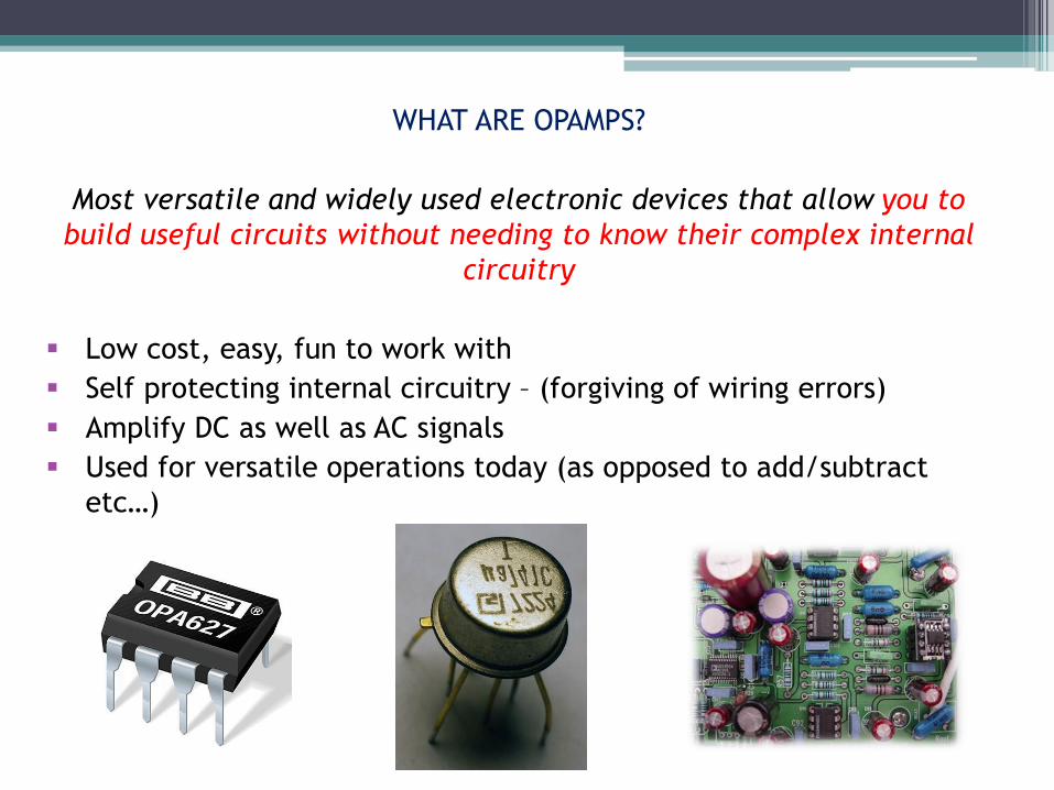
WHAT ARE OPAMPS?
Most versatile and widely used electronic devices that allow you to
build useful circuits without needing to know their complex internal
circuitry
Low cost, easy, fun to work with
Self protecting internal circuitry – (forgiving of wiring errors)
Amplify DC as well as AC signals
Used for versatile operations today (as opposed to add/subtract
etc…)
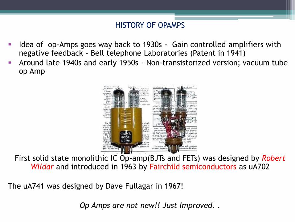
HISTORY OF OPAMPS
Idea of op-Amps goes way back to 1930s - Gain controlled amplifiers with negative feedback - Bell telephone Laboratories (Patent in 1941)
Around late 1940s and early 1950s - Non-transistorized version; vacuum tube op Amp
First solid state monolithic IC Op-amp(BJTs and FETs) was designed by Robert Wildar and introduced in 1963 by Fairchild semiconductors as uA702
The uA741 was designed by Dave Fullagar in 1967!
Op Amps are not new!! Just Improved. .
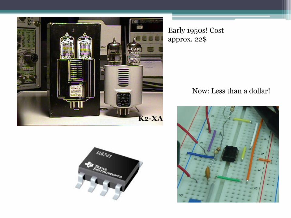
K2-XA
Early 1950s! Cost approx. 22$
Now: Less than a dollar!
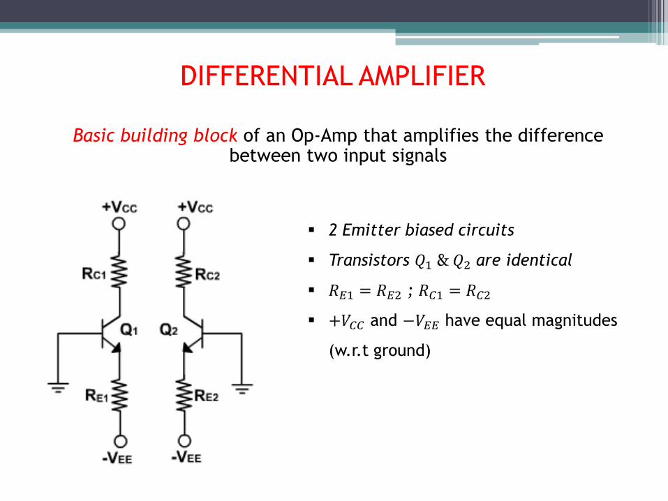
DIFFERENTIAL AMPLIFIER
Basic building block of an Op-Amp that amplifies the difference between two input signals
2 Emitter biased circuits
Transistors 𝑄1 & 𝑄2 are identical
𝑅𝐸1 = 𝑅𝐸2 ; 𝑅𝐶1 = 𝑅𝐶2
+𝑉𝐶𝐶 and −𝑉𝐸𝐸 have equal magnitudes
(w.r.t ground)
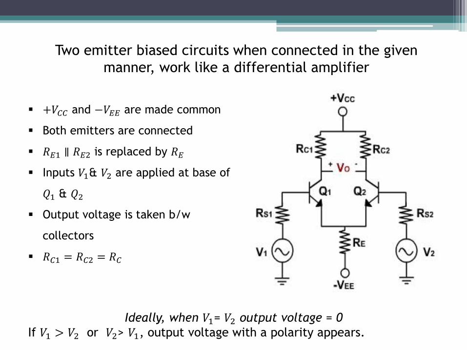
Two emitter biased circuits when connected in the given
manner, work like a differential amplifier
+𝑉𝐶𝐶 and −𝑉𝐸𝐸 are made common
Both emitters are connected
𝑅𝐸1 ∥ 𝑅𝐸2 is replaced by 𝑅𝐸
Inputs 𝑉1& 𝑉2 are applied at base of
𝑄1 & 𝑄2
Output voltage is taken b/w
collectors
𝑅𝐶1 = 𝑅𝐶2 = 𝑅𝐶
Ideally, when 𝑉1= 𝑉2 output voltage = 0
If 𝑉1 > 𝑉2 or 𝑉2> 𝑉1, output voltage with a polarity appears.
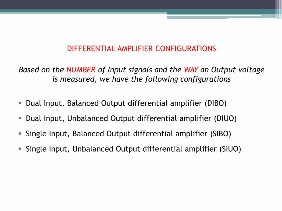
DIFFERENTIAL AMPLIFIER CONFIGURATIONS
Based on the NUMBER of Input signals and the WAY an Output voltage
is measured, we have the following configurations
Dual Input, Balanced Output differential amplifier (DIBO)
Dual Input, Unbalanced Output differential amplifier (DIUO)
Single Input, Balanced Output differential amplifier (SIBO)
Single Input, Unbalanced Output differential amplifier (SIUO)
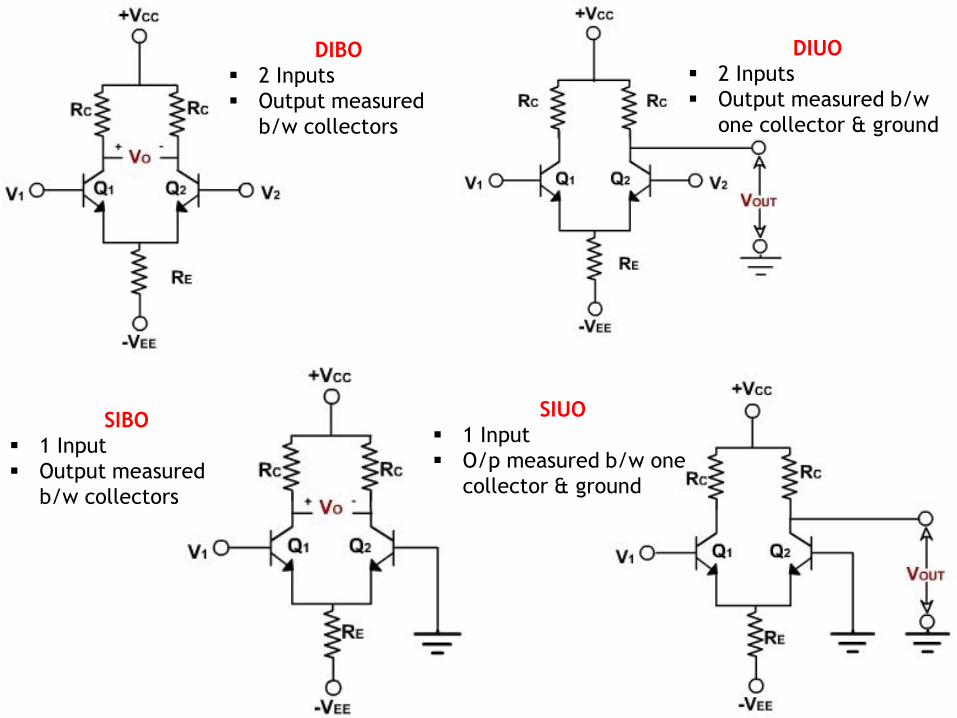
DIBO
2 Inputs
Output measured
b/w collectors
DIUO
2 Inputs
Output measured b/w
one collector & ground
SIBO
1 Input
Output measured
b/w collectors
SIUO
1 Input
O/p measured b/w one
collector & ground
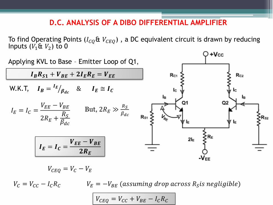
D.C. ANALYSIS OF A DIBO DIFFERENTIAL AMPLIFIER
To find Operating Points (𝐼𝐶𝑄& 𝑉𝐶𝐸𝑄) , a DC equivalent circuit is drawn by reducing Inputs (𝑉1& 𝑉2) to 0 Applying KVL to Base – Emitter Loop of Q1,
W.K.T, 𝑰𝑩 = 𝑰𝑬𝜷𝒅𝒄 & 𝑰𝑬 ≅ 𝑰𝑪
𝐼𝐸 = 𝐼𝐶 =𝑉𝐸𝐸 − 𝑉𝐵𝐸
2𝑅𝐸 +𝑅𝑆𝛽𝑑𝑐
𝑰𝑩𝑹𝑺𝟏 + 𝑽𝑩𝑬 + 𝟐𝑰𝑬𝑹𝑬 = 𝑽𝑬𝑬
𝑉𝐶𝐸𝑄 = 𝑉𝐶 − 𝑉𝐸
𝑉𝐶 = 𝑉𝐶𝐶 − 𝐼𝐶𝑅𝐶 𝑉𝐸 = −𝑉𝐵𝐸 (𝑎𝑠𝑠𝑢𝑚𝑖𝑛𝑔 𝑑𝑟𝑜𝑝 𝑎𝑐𝑟𝑜𝑠𝑠 𝑅𝑆𝑖𝑠 𝑛𝑒𝑔𝑙𝑖𝑔𝑖𝑏𝑙𝑒)
𝑉𝐶𝐸𝑄 = 𝑉𝐶𝐶 + 𝑉𝐵𝐸 − 𝐼𝐶𝑅𝐶
𝑰𝑬 = 𝑰𝑪 =𝑽𝑬𝑬 − 𝑽𝑩𝑬
𝟐𝑹𝑬
But, 2𝑅𝐸 ≫𝑅𝑆
𝛽𝑑𝑐
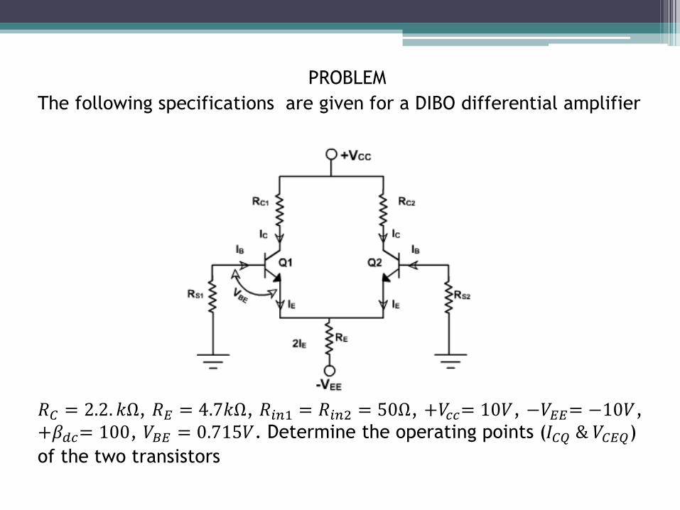
PROBLEM
The following specifications are given for a DIBO differential amplifier
𝑅𝐶 = 2.2. 𝑘Ω, 𝑅𝐸 = 4.7𝑘Ω, 𝑅𝑖𝑛1 = 𝑅𝑖𝑛2 = 50Ω, +𝑉𝑐𝑐= 10𝑉, −𝑉𝐸𝐸= −10𝑉,
+𝛽𝑑𝑐= 100, 𝑉𝐵𝐸 = 0.715𝑉. Determine the operating points (𝐼𝐶𝑄 & 𝑉𝐶𝐸𝑄)
of the two transistors
OPERATIONAL AMPLIFIER
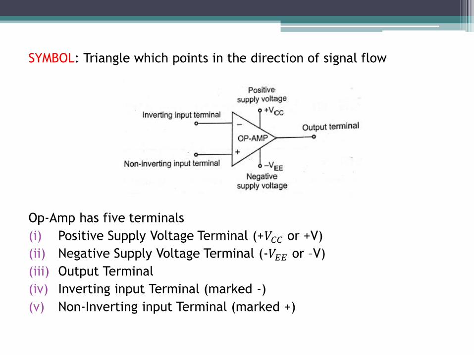
SYMBOL: Triangle which points in the direction of signal flow
Op-Amp has five terminals
(i) Positive Supply Voltage Terminal (+𝑉𝐶𝐶 or +V)
(ii) Negative Supply Voltage Terminal (-𝑉𝐸𝐸 or –V)
(iii) Output Terminal
(iv) Inverting input Terminal (marked -)
(v) Non-Inverting input Terminal (marked +)
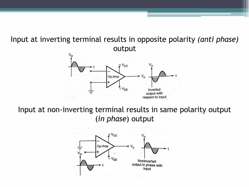
Input at inverting terminal results in opposite polarity (anti phase)
output
Input at non-inverting terminal results in same polarity output
(in phase) output
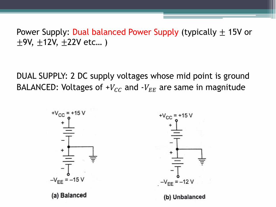
Power Supply: Dual balanced Power Supply (typically ± 15V or
±9V, ±12V, ±22V etc… )
DUAL SUPPLY: 2 DC supply voltages whose mid point is ground
BALANCED: Voltages of +𝑉𝐶𝐶 and -𝑉𝐸𝐸 are same in magnitude
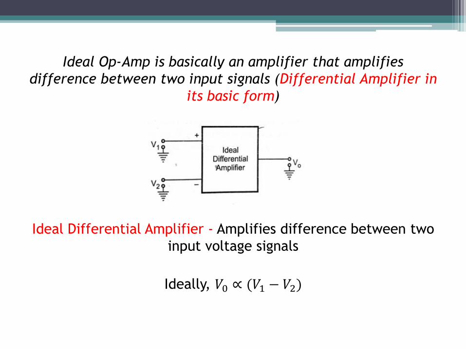
Ideal Op-Amp is basically an amplifier that amplifies
difference between two input signals (Differential Amplifier in
its basic form)
Ideal Differential Amplifier - Amplifies difference between two
input voltage signals
Ideally, 𝑉0 ∝ (𝑉1 − 𝑉2)
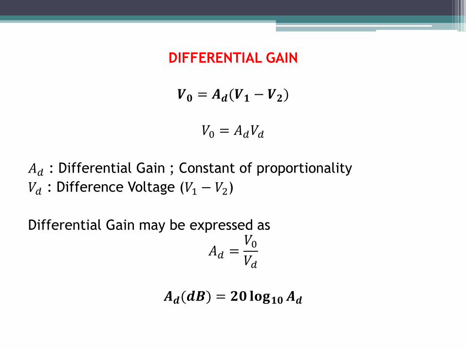
DIFFERENTIAL GAIN
𝑽𝟎 = 𝑨𝒅(𝑽𝟏 − 𝑽𝟐)
𝑉0 = 𝐴𝑑𝑉𝑑
𝐴𝑑 : Differential Gain ; Constant of proportionality
𝑉𝑑 : Difference Voltage (𝑉1 − 𝑉2)
Differential Gain may be expressed as
𝐴𝑑 =𝑉0𝑉𝑑
𝑨𝒅(𝒅𝑩) = 𝟐𝟎 𝐥𝐨𝐠𝟏𝟎𝑨𝒅
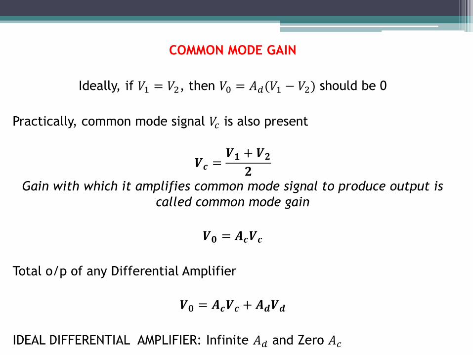
COMMON MODE GAIN
Ideally, if 𝑉1 = 𝑉2, then 𝑉0 = 𝐴𝑑(𝑉1 − 𝑉2) should be 0
Practically, common mode signal 𝑉𝑐 is also present
𝑽𝒄 =𝑽𝟏 + 𝑽𝟐
𝟐
Gain with which it amplifies common mode signal to produce output is
called common mode gain
𝑽𝟎 = 𝑨𝒄𝑽𝒄
Total o/p of any Differential Amplifier
𝑽𝟎 = 𝑨𝒄𝑽𝒄 + 𝑨𝒅𝑽𝒅
IDEAL DIFFERENTIAL AMPLIFIER: Infinite 𝐴𝑑 and Zero 𝐴𝑐
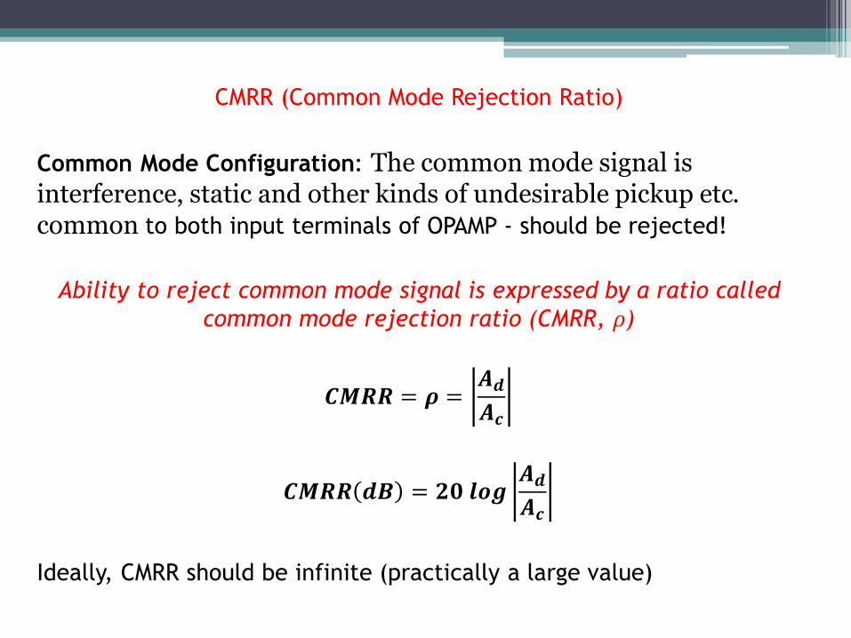
CMRR (Common Mode Rejection Ratio)
Common Mode Configuration: The common mode signal is interference, static and other kinds of undesirable pickup etc. common to both input terminals of OPAMP - should be rejected!
Ability to reject common mode signal is expressed by a ratio called
common mode rejection ratio (CMRR, 𝜌)
𝑪𝑴𝑹𝑹 = 𝝆 =𝑨𝒅
𝑨𝒄
𝑪𝑴𝑹𝑹 𝒅𝑩 = 𝟐𝟎 𝒍𝒐𝒈𝑨𝒅
𝑨𝒄
Ideally, CMRR should be infinite (practically a large value)
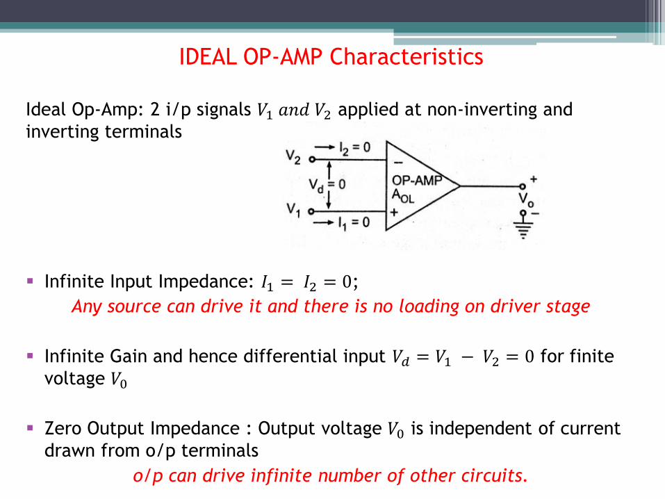
IDEAL OP-AMP Characteristics
Ideal Op-Amp: 2 i/p signals 𝑉1 𝑎𝑛𝑑 𝑉2 applied at non-inverting and
inverting terminals
Infinite Input Impedance: 𝐼1 = 𝐼2 = 0;
Any source can drive it and there is no loading on driver stage
Infinite Gain and hence differential input 𝑉𝑑 = 𝑉1 − 𝑉2 = 0 for finite
voltage 𝑉0
Zero Output Impedance : Output voltage 𝑉0 is independent of current
drawn from o/p terminals
o/p can drive infinite number of other circuits.
The various characteristics of an Ideal Op-Amp are
Infinite Voltage Gain
Infinite Input Impedance
Zero Output Impedance
Zero Offset Voltage
Infinite Bandwidth
Infinite CMRR
Infinite Slew Rate
No effect of Temperature
Power Supply Rejection Ratio
Infinite Voltage Gain (𝐴𝑂𝐿): Differential Open Loop Gain and is
infinite for an ideal Op-Amp.
Infinite Input Impedance (𝑅𝑖𝑛): Infinite for ideal Op-Amp and
ensures that no current flows into an ideal Op-Amp
Zero Output Impedance (𝑅𝑂): Zero for an ideal Op-Amp and ensures
that o/p voltage of an Op-Amp remains the same irrespective of
the value of the load resistance connected
Zero Offset Voltage: Presence of a small output voltage even if
𝑉1 − 𝑉2 = 0 is called ‘Offset Voltage’ - Zero for an Ideal Op-Amp
Ensures that output is zero for zero input signal
Infinite Bandwidth:
Bandwidth: Range of frequency over which satisfactory amplifier performance
is obtained
Infinite Bandwidth implies Operating frequency range is 0 to ∞
Ensures that gain of Op-Amp will be constant over freq. range from DC
frequency (0) to infinite frequency
Amplify AC as well as DC
Infinite CMRR: Infinite for ideal Op-Amp and ensures Zero Noise output voltage
( 𝐴𝐶 = 0)
Infinite Slew Rate:
Slew Rate: Maximum rate of change of output voltage with time - 𝑉 𝜇𝑠
𝑆𝑙𝑒𝑤 𝑅𝑎𝑡𝑒 𝑆 =𝑑𝑉0𝑑𝑡
(𝑚𝑎𝑥𝑖𝑚𝑢𝑚)
Infinite Slew Rate implies changes in the output voltage occurs simultaneously
with changes in the input voltage. (e.g. Step Input)
No effect of temperature: Characteristics of an op-amp does not
change with temperature
Power Supply Rejection Ratio (PSRR): This is defined as ratio of
change in input offset voltage due to changes in supply voltage
producing it, keeping other power supply voltage constant (Power
Supply Sensitivity)
If 𝑉𝐸𝐸 is constant and due to change in 𝑉𝐶𝐶, there is change in
input offset voltage, then PSRR is expressed as,
𝑃𝑆𝑅𝑅 =∆𝑉𝑖𝑜𝑠∆𝑉𝐶𝐶
(𝑚𝑉𝑉 𝑜𝑟
𝜇𝑉𝑉 )
Similarly,
𝑃𝑆𝑅𝑅 =∆𝑉𝑖𝑜𝑠∆𝑉𝐸𝐸
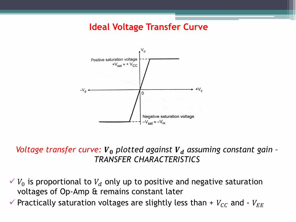
Ideal Voltage Transfer Curve
Voltage transfer curve: 𝑽𝟎 plotted against 𝑽𝒅 assuming constant gain –
TRANSFER CHARACTERISTICS
𝑉0 is proportional to 𝑉𝑑 only up to positive and negative saturation
voltages of Op-Amp & remains constant later
Practically saturation voltages are slightly less than + 𝑉𝐶𝐶 and - 𝑉𝐸𝐸
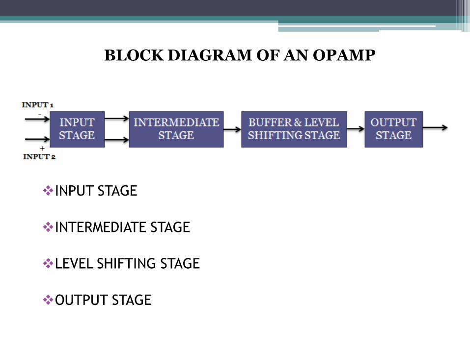
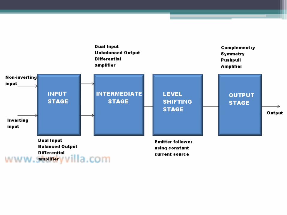
BLOCK DIAGRAM OF AN OPAMP
INPUT STAGE
INTERMEDIATE STAGE
LEVEL SHIFTING STAGE
OUTPUT STAGE
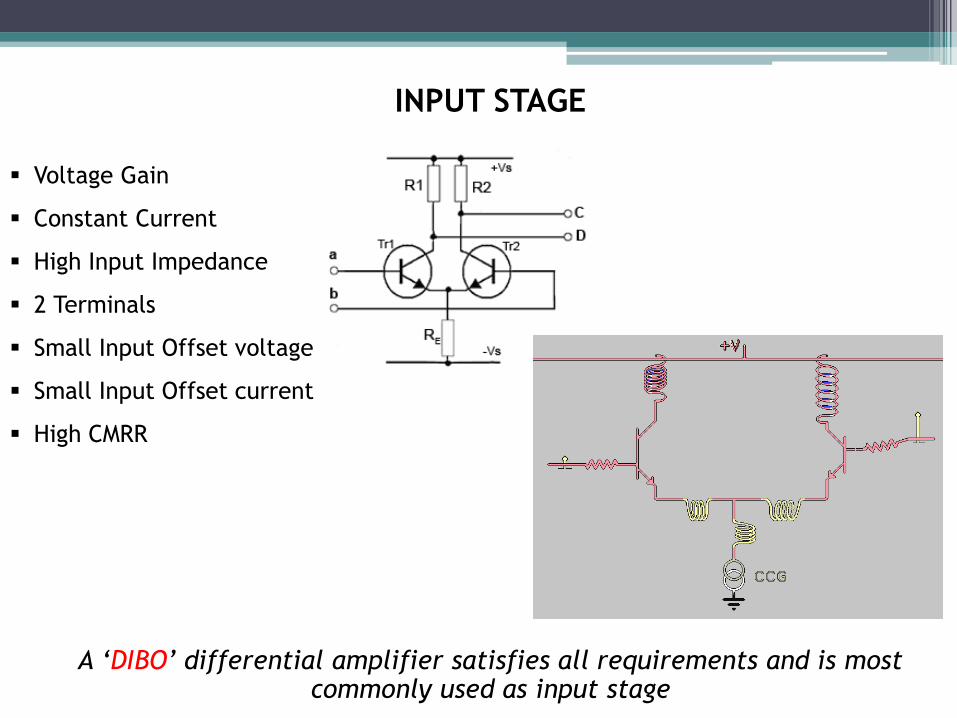
INPUT STAGE
A ‘DIBO’ differential amplifier satisfies all requirements and is most commonly used as input stage
Voltage Gain
Constant Current
High Input Impedance
2 Terminals
Small Input Offset voltage
Small Input Offset current
High CMRR
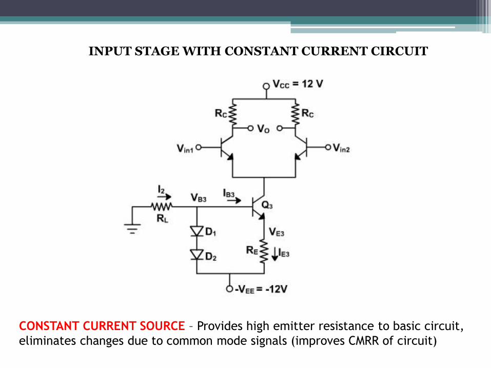
CONSTANT CURRENT SOURCE – Provides high emitter resistance to basic circuit,
eliminates changes due to common mode signals (improves CMRR of circuit)
INPUT STAGE WITH CONSTANT CURRENT CIRCUIT
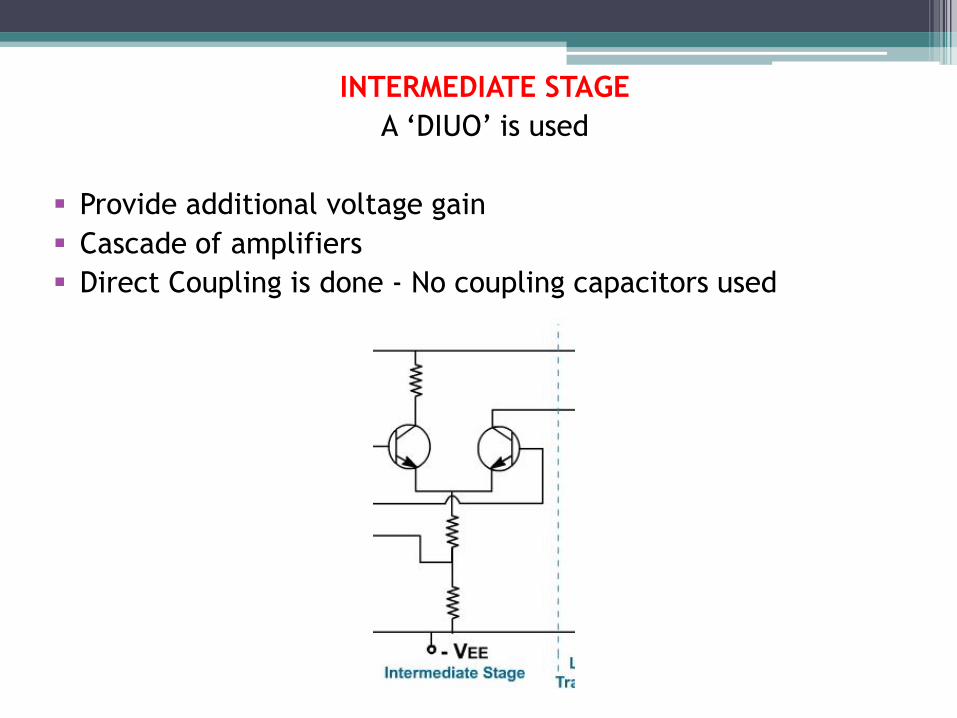
INTERMEDIATE STAGE
A ‘DIUO’ is used
Provide additional voltage gain
Cascade of amplifiers
Direct Coupling is done - No coupling capacitors used
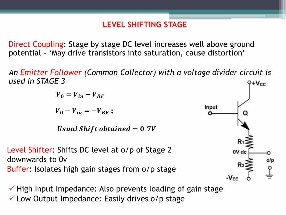
LEVEL SHIFTING STAGE
Direct Coupling: Stage by stage DC level increases well above ground potential - ‘May drive transistors into saturation, cause distortion’
An Emitter Follower (Common Collector) with a voltage divider circuit is used in STAGE 3
High Input Impedance: Also prevents loading of gain stage
Low Output Impedance: Easily drives o/p stage
Level Shifter: Shifts DC level at o/p of Stage 2
downwards to 0v
Buffer: Isolates high gain stages from o/p stage
𝑽𝟎 = 𝑽𝒊𝒏 − 𝑽𝑩𝑬
𝑽𝟎 − 𝑽𝒊𝒏 = −𝑽𝑩𝑬 ;
𝑼𝒔𝒖𝒂𝒍 𝑺𝒉𝒊𝒇𝒕 𝒐𝒃𝒕𝒂𝒊𝒏𝒆𝒅 = 𝟎. 𝟕𝑽
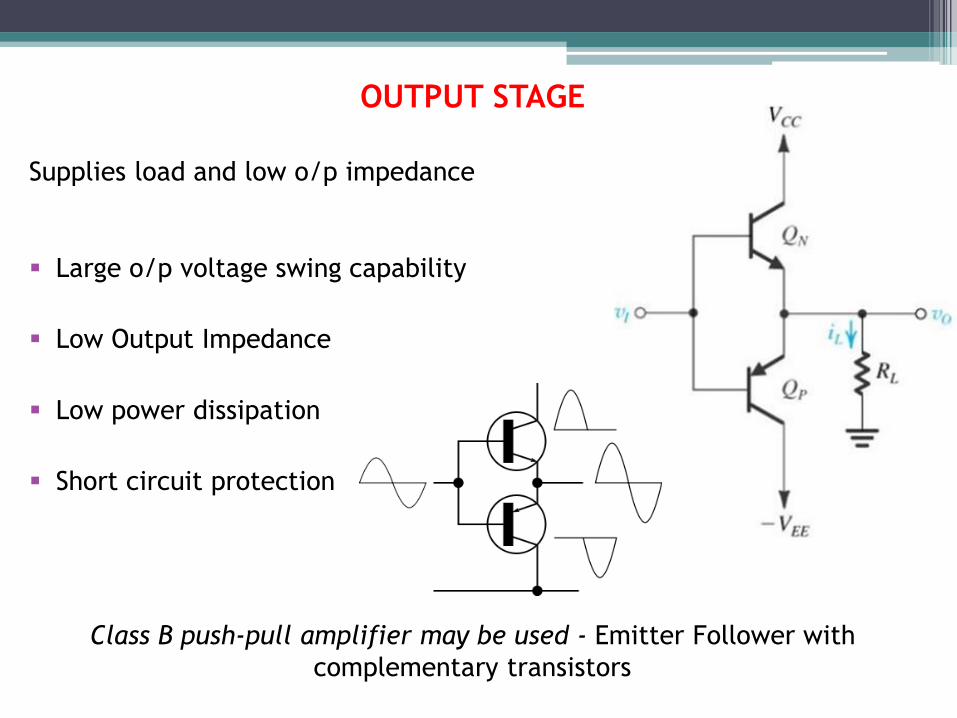
OUTPUT STAGE
Supplies load and low o/p impedance
Large o/p voltage swing capability
Low Output Impedance
Low power dissipation
Short circuit protection
Class B push-pull amplifier may be used - Emitter Follower with
complementary transistors
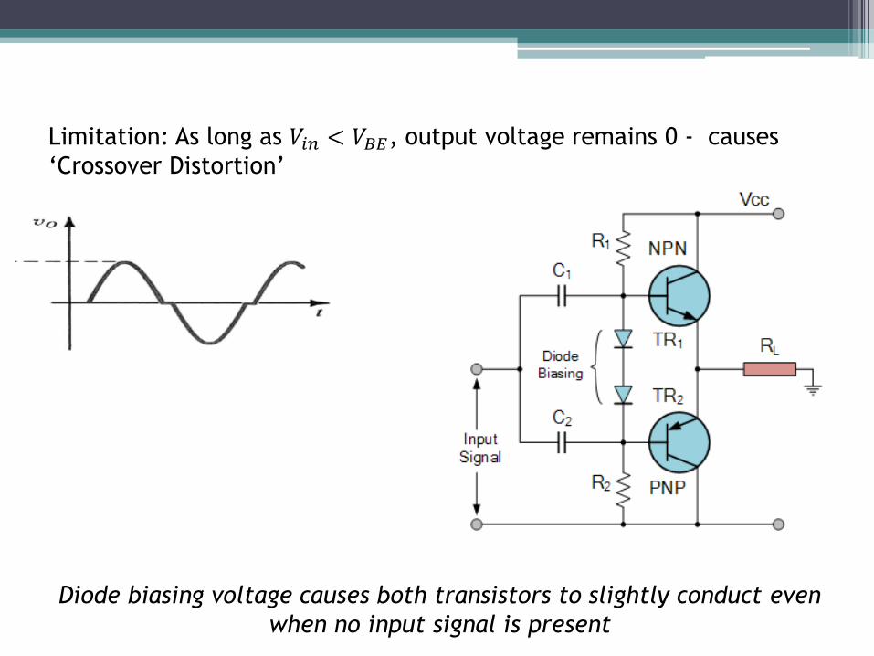
Limitation: As long as 𝑉𝑖𝑛 < 𝑉𝐵𝐸, output voltage remains 0 - causes
‘Crossover Distortion’
Diode biasing voltage causes both transistors to slightly conduct even
when no input signal is present
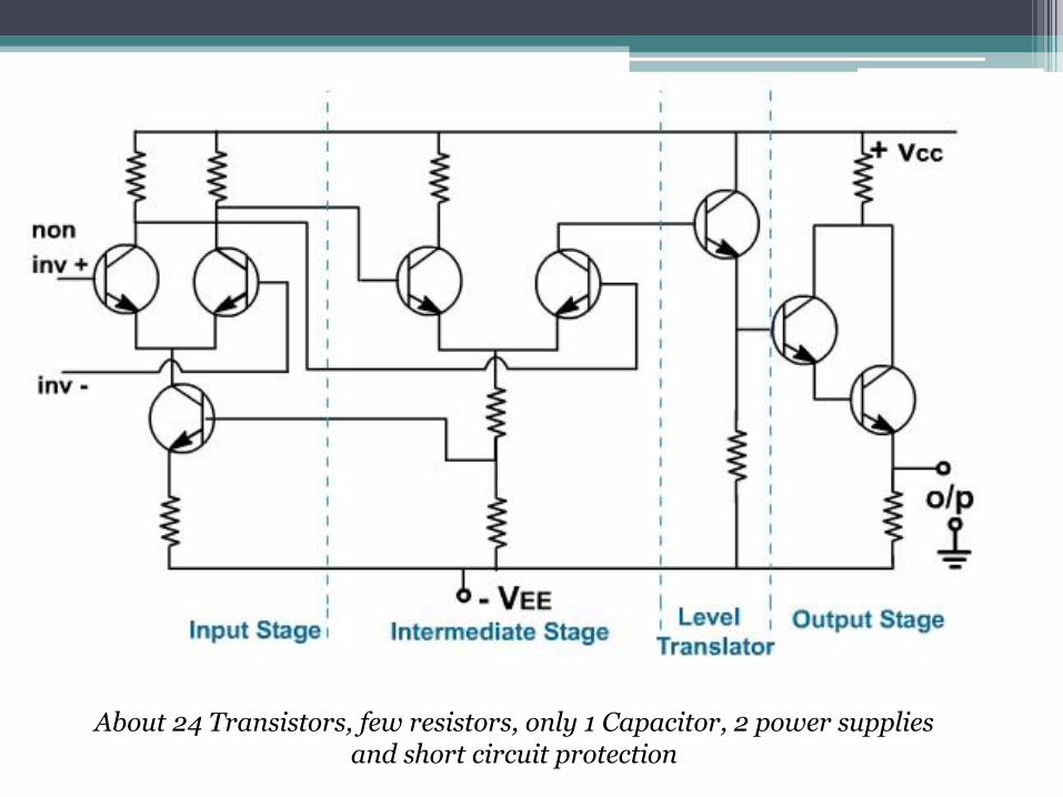
About 24 Transistors, few resistors, only 1 Capacitor, 2 power supplies and short circuit protection
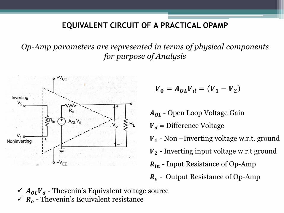
EQUIVALENT CIRCUIT OF A PRACTICAL OPAMP
Op-Amp parameters are represented in terms of physical components for purpose of Analysis
𝑽𝟎 = 𝑨𝑶𝑳𝑽𝒅 = 𝑽𝟏 − 𝑽𝟐
𝑨𝑶𝑳 - Open Loop Voltage Gain
𝑽𝒅 = Difference Voltage
𝑽𝟏 - Non –Inverting voltage w.r.t. ground
𝑽𝟐 - Inverting input voltage w.r.t ground
𝑹𝒊𝒏 - Input Resistance of Op-Amp
𝑹𝒐 - Output Resistance of Op-Amp
𝑨𝑶𝑳𝑽𝒅 - Thevenin’s Equivalent voltage source 𝑹𝒐 - Thevenin’s Equivalent resistance
PRACTICAL OP-AMP CHARACTERISTICS
OPEN LOOP GAIN: Voltage gain of op-amp without feedback (several thousands)
INPUT IMPEDANCE: Finite (>1MΩ and may be increased to several M𝜴 if FETs are
used in input stage)
OUTPUT IMPEDANCE: Finite (few 100 Ω and may be reduced to 1 - 2 Ω using
negative feedback)
BANDWIDTH: Finite and small in O.L. configuration (may be increased to a suitable
value by using a negative feedback)
INPUT OFFSET VOLTAGE: A small non-zero o/p voltage is present even if both i/p
terminals are grounded (ideally 0)
The D.C. voltage applied to a particular terminal that makes o/p voltage 0 when
other terminal is grounded is called Input Offset Voltage 𝑉𝑖𝑜𝑠
Voltage, terminal, polarity etc specified by manufacturer
INPUT BIAS CURRENT: Practical Op-Amps have some current flowing into
the input terminals (10−6 − 10−14𝐴)
Due to improper matching of transistors, I/p terminals (base terminals
of 2 transistors) conduct small amount of d.c. currents known as bias
currents (𝐼𝑏1𝑎𝑛𝑑𝐼𝑏2)
Manufacturers specify average bias current 𝐼𝑏
𝑰𝒃 =𝑰𝒃𝟏 + 𝑰𝒃𝟐
𝟐
Transistors of the Differential Amplifier (used as i/p stages) must be
biased correctly
INPUT OFFSET CURRENT: Difference in magnitudes of 𝐼𝑏1 and 𝐼𝑏2 is called Input Offset Current
𝑰𝒊𝒐𝒔 = 𝑰𝒃𝟏 − 𝑰𝒃𝟐
Magnitude: Small (20 – 60 nA) when input Vg = 0
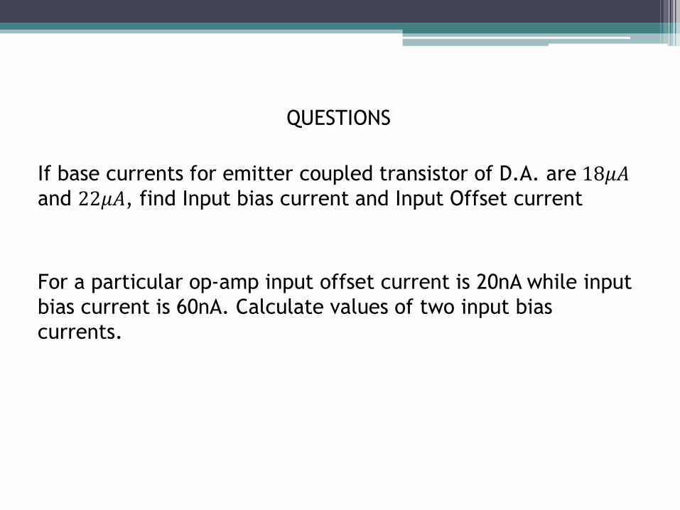
QUESTIONS
If base currents for emitter coupled transistor of D.A. are 18𝜇𝐴
and 22𝜇𝐴, find Input bias current and Input Offset current
For a particular op-amp input offset current is 20nA while input
bias current is 60nA. Calculate values of two input bias
currents.
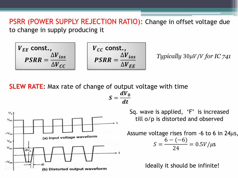
PSRR (POWER SUPPLY REJECTION RATIO): Change in offset voltage due
to change in supply producing it
SLEW RATE: Max rate of change of output voltage with time
𝑺 =𝒅𝑽𝟎
𝒅𝒕
𝑽𝑬𝑬 const.,
𝑷𝑺𝑹𝑹 =∆𝑽𝒊𝒐𝒔
∆𝑽𝑪𝑪
𝑽𝑪𝑪 const.,
𝑷𝑺𝑹𝑹 =∆𝑽𝒊𝒐𝒔
∆𝑽𝑬𝑬
Typically 30𝜇𝑉/𝑉 for IC 741
Sq. wave is applied, ‘F’ is increased
till o/p is distorted and observed
Assume voltage rises from -6 to 6 in 24𝜇s,
𝑆 =6 − (−6)
24= 0.5𝑉/𝜇s
Ideally it should be infinite!
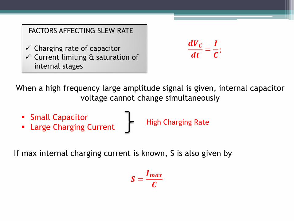
When a high frequency large amplitude signal is given, internal capacitor
voltage cannot change simultaneously
If max internal charging current is known, S is also given by
𝑺 =𝑰𝒎𝒂𝒙
𝑪
FACTORS AFFECTING SLEW RATE
Charging rate of capacitor
Current limiting & saturation of
internal stages
𝒅𝑽𝑪
𝒅𝒕=
𝑰
𝑪;
Small Capacitor
Large Charging Current High Charging Rate
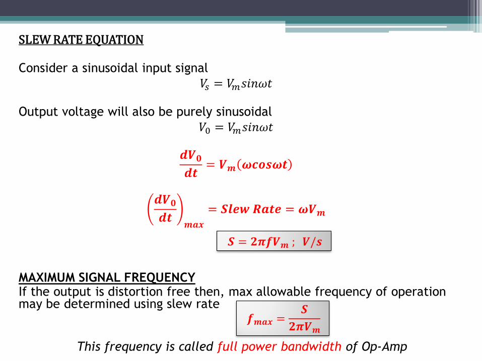
SLEW RATE EQUATION Consider a sinusoidal input signal
𝑉𝑠 = 𝑉𝑚𝑠𝑖𝑛𝜔𝑡 Output voltage will also be purely sinusoidal
𝑉0 = 𝑉𝑚𝑠𝑖𝑛𝜔𝑡
𝒅𝑽𝟎
𝒅𝒕= 𝑽𝒎 𝝎𝒄𝒐𝒔𝝎𝒕
𝒅𝑽𝟎
𝒅𝒕𝒎𝒂𝒙
= 𝑺𝒍𝒆𝒘 𝑹𝒂𝒕𝒆 = 𝝎𝑽𝒎
MAXIMUM SIGNAL FREQUENCY If the output is distortion free then, max allowable frequency of operation may be determined using slew rate
This frequency is called full power bandwidth of Op-Amp
𝑺 = 𝟐𝝅𝒇𝑽𝒎 ; 𝑽/𝒔
𝒇𝒎𝒂𝒙 =𝑺
𝟐𝝅𝑽𝒎
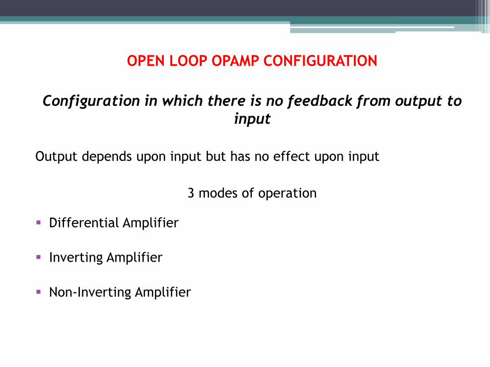
OPEN LOOP OPAMP CONFIGURATION
Configuration in which there is no feedback from output to
input
Output depends upon input but has no effect upon input
3 modes of operation
Differential Amplifier
Inverting Amplifier
Non-Inverting Amplifier
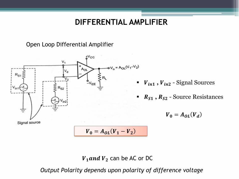
DIFFERENTIAL AMPLIFIER
Open Loop Differential Amplifier
𝑽𝟎 = 𝑨𝑶𝑳 𝑽𝟏 − 𝑽𝟐
𝑽𝟎 = 𝑨𝑶𝑳 𝑽𝒅
𝑽𝒊𝒏𝟏 , 𝑽𝒊𝒏𝟐 - Signal Sources 𝑹𝑺𝟏 , 𝑹𝑺𝟐 - Source Resistances
𝑽𝟏𝒂𝒏𝒅 𝑽𝟐 can be AC or DC
Output Polarity depends upon polarity of difference voltage
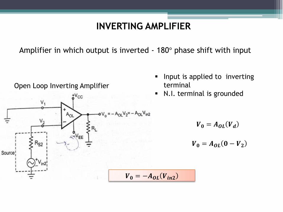
INVERTING AMPLIFIER
Amplifier in which output is inverted - 180° phase shift with input
Open Loop Inverting Amplifier
𝑽𝟎 = 𝑨𝑶𝑳 𝟎 − 𝑽𝟐
𝑽𝟎 = 𝑨𝑶𝑳 𝑽𝒅
Input is applied to inverting
terminal
N.I. terminal is grounded
𝑽𝟎 = −𝑨𝑶𝑳 𝑽𝒊𝒏𝟐
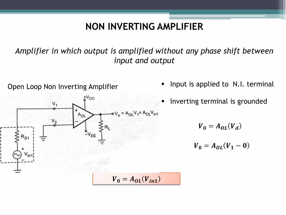
NON INVERTING AMPLIFIER
Amplifier in which output is amplified without any phase shift between
input and output
Open Loop Non Inverting Amplifier
𝑽𝟎 = 𝑨𝑶𝑳 𝑽𝟏 − 𝟎
𝑽𝟎 = 𝑨𝑶𝑳 𝑽𝒅
Input is applied to N.I. terminal
Inverting terminal is grounded
𝑽𝟎 = 𝑨𝑶𝑳 𝑽𝒊𝒏𝟏
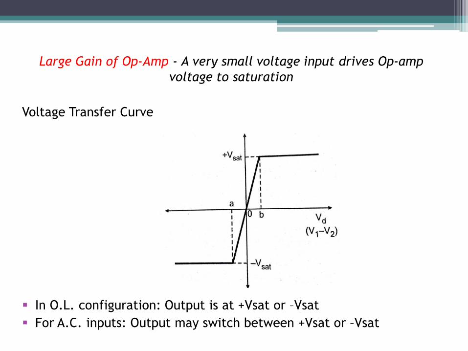
Large Gain of Op-Amp - A very small voltage input drives Op-amp
voltage to saturation
Voltage Transfer Curve
In O.L. configuration: Output is at +Vsat or –Vsat
For A.C. inputs: Output may switch between +Vsat or –Vsat
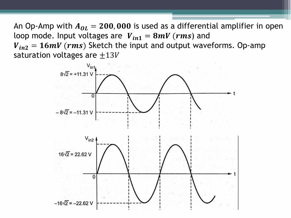
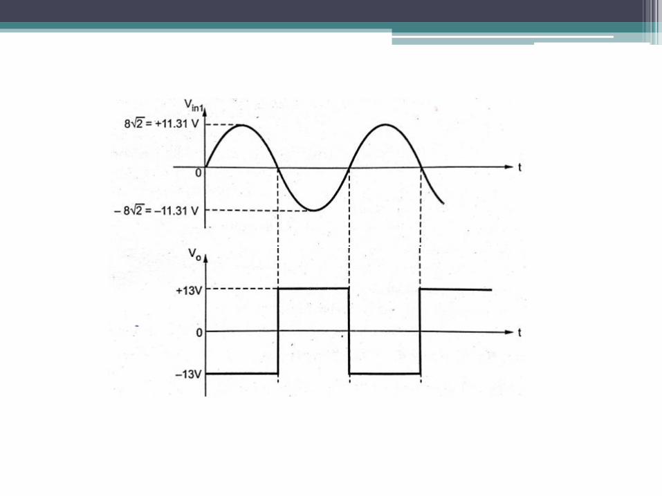
An Op-Amp with 𝑨𝑶𝑳 = 𝟐𝟎𝟎, 𝟎𝟎𝟎 is used as a differential amplifier in open
loop mode. Input voltages are 𝑽𝒊𝒏𝟏 = 𝟖𝒎𝑽 (𝒓𝒎𝒔) and
𝑽𝒊𝒏𝟐 = 𝟏𝟔𝒎𝑽 (𝒓𝒎𝒔) Sketch the input and output waveforms. Op-amp
saturation voltages are ±13𝑉
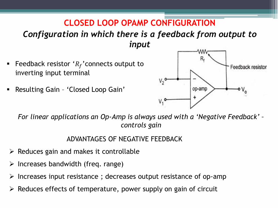
CLOSED LOOP OPAMP CONFIGURATION
Configuration in which there is a feedback from output to
input
Feedback resistor ‘𝑅𝑓’connects output to
inverting input terminal
Resulting Gain – ‘Closed Loop Gain’
For linear applications an Op-Amp is always used with a ‘Negative Feedback’ –
controls gain
ADVANTAGES OF NEGATIVE FEEDBACK
Reduces gain and makes it controllable
Increases bandwidth (freq. range)
Increases input resistance ; decreases output resistance of op-amp
Reduces effects of temperature, power supply on gain of circuit
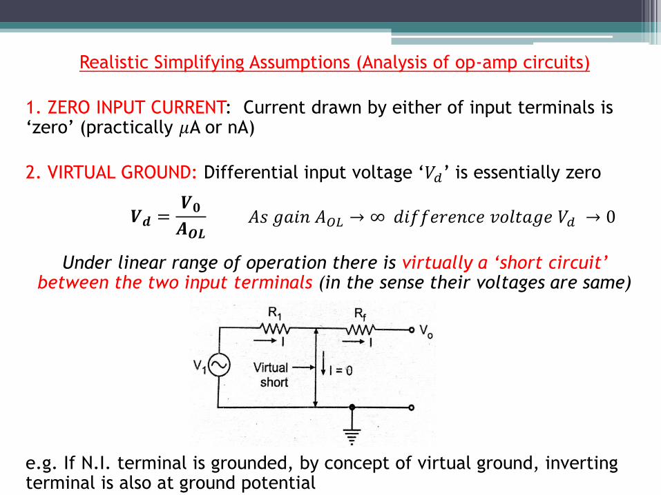
Realistic Simplifying Assumptions (Analysis of op-amp circuits)
1. ZERO INPUT CURRENT: Current drawn by either of input terminals is ‘zero’ (practically 𝜇A or nA)
2. VIRTUAL GROUND: Differential input voltage ‘𝑉𝑑’ is essentially zero
Under linear range of operation there is virtually a ‘short circuit’ between the two input terminals (in the sense their voltages are same)
e.g. If N.I. terminal is grounded, by concept of virtual ground, inverting terminal is also at ground potential
𝐴𝑠 𝑔𝑎𝑖𝑛 𝐴𝑂𝐿 → ∞ 𝑑𝑖𝑓𝑓𝑒𝑟𝑒𝑛𝑐𝑒 𝑣𝑜𝑙𝑡𝑎𝑔𝑒 𝑉𝑑 → 0 𝑽𝒅 =𝑽𝟎
𝑨𝑶𝑳
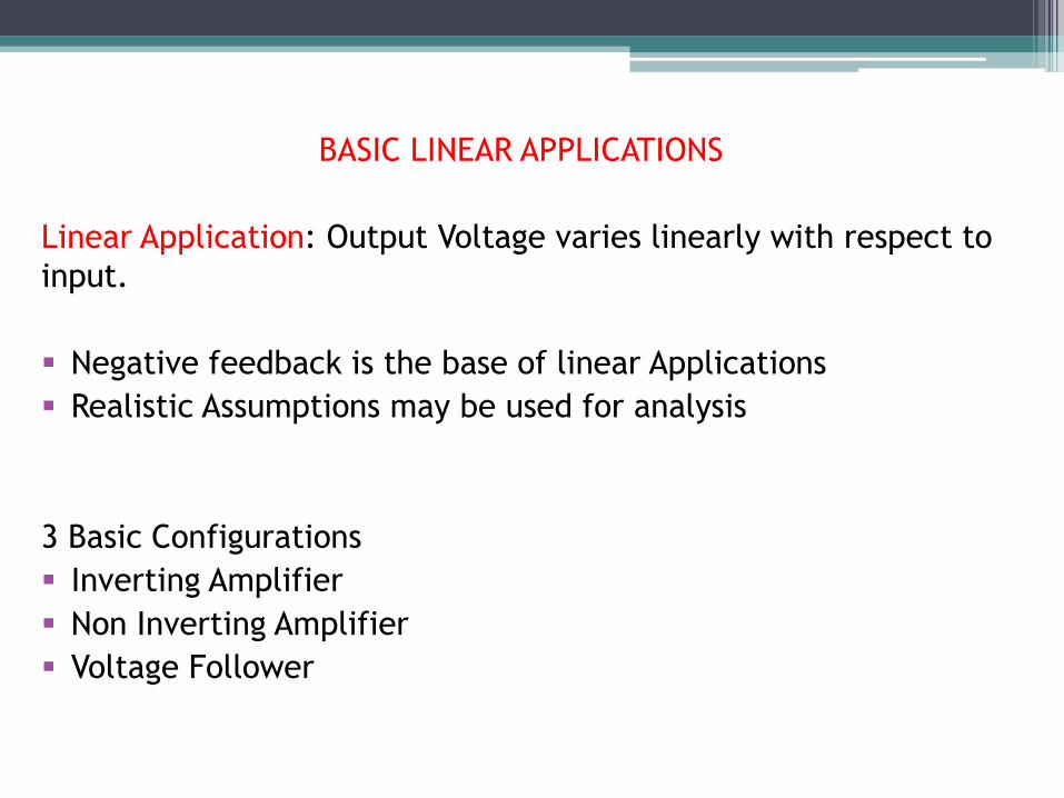
BASIC LINEAR APPLICATIONS
Linear Application: Output Voltage varies linearly with respect to
input.
Negative feedback is the base of linear Applications
Realistic Assumptions may be used for analysis
3 Basic Configurations
Inverting Amplifier
Non Inverting Amplifier
Voltage Follower
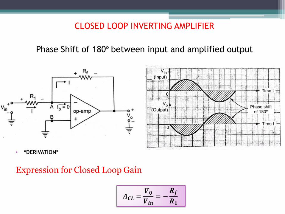
CLOSED LOOP INVERTING AMPLIFIER
Phase Shift of 180° between input and amplified output
• *DERIVATION*
Expression for Closed Loop Gain
𝑨𝑪𝑳 =𝑽𝟎
𝑽𝒊𝒏= −
𝑹𝒇
𝑹𝟏
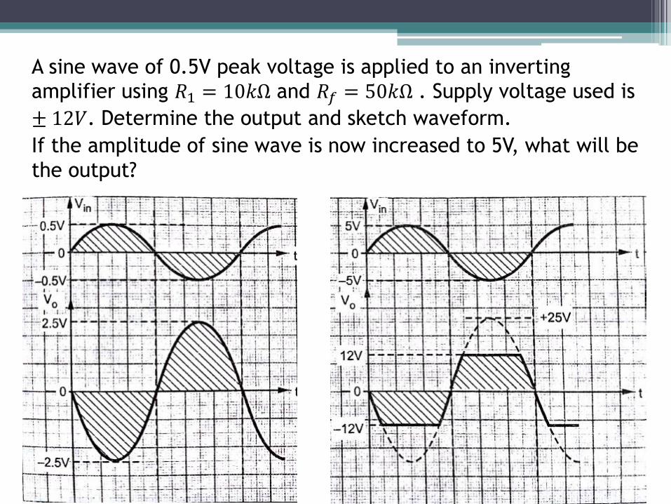
A sine wave of 0.5V peak voltage is applied to an inverting
amplifier using 𝑅1 = 10𝑘Ω and 𝑅𝑓 = 50𝑘Ω . Supply voltage used is
± 12𝑉. Determine the output and sketch waveform.
If the amplitude of sine wave is now increased to 5V, what will be
the output?
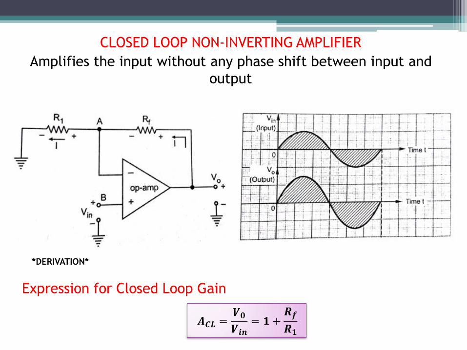
CLOSED LOOP NON-INVERTING AMPLIFIER
Amplifies the input without any phase shift between input and
output
Expression for Closed Loop Gain
*DERIVATION*
𝑨𝑪𝑳 =𝑽𝟎
𝑽𝒊𝒏= 𝟏 +
𝑹𝒇
𝑹𝟏
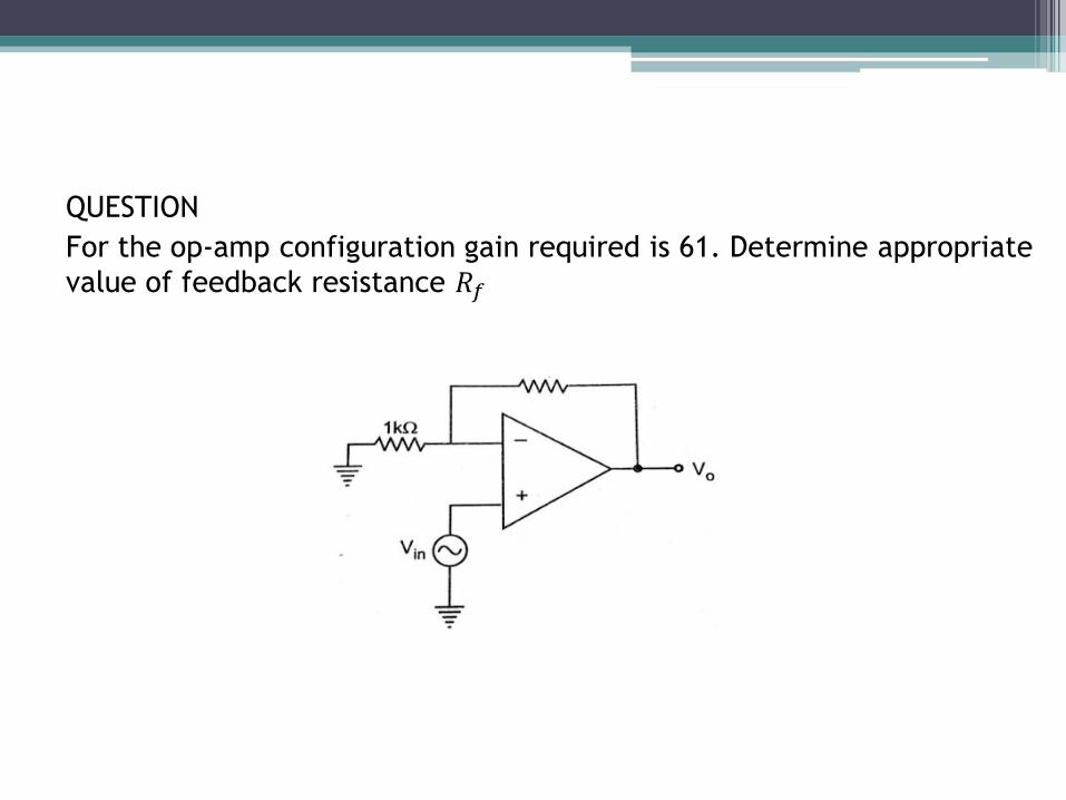
QUESTION
For the op-amp configuration gain required is 61. Determine appropriate
value of feedback resistance 𝑅𝑓
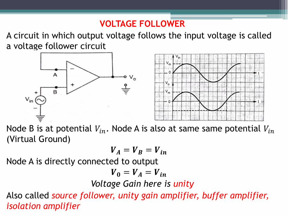
VOLTAGE FOLLOWER
A circuit in which output voltage follows the input voltage is called
a voltage follower circuit
Node B is at potential 𝑉𝑖𝑛. Node A is also at same same potential 𝑉𝑖𝑛
(Virtual Ground)
𝑽𝑨 = 𝑽𝑩 = 𝑽𝒊𝒏
Node A is directly connected to output
𝑽𝟎 = 𝑽𝑨 = 𝑽𝒊𝒏
Voltage Gain here is unity
Also called source follower, unity gain amplifier, buffer amplifier,
isolation amplifier
ACTIVITY: Find out advantages/applications of a voltage follower circuit
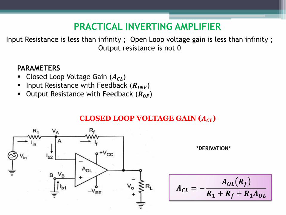
PRACTICAL INVERTING AMPLIFIER
Input Resistance is less than infinity ; Open Loop voltage gain is less than infinity ;
Output resistance is not 0
𝑨𝑪𝑳 = −𝑨𝑶𝑳 𝑹𝒇
𝑹𝟏 + 𝑹𝒇 + 𝑹𝟏𝑨𝑶𝑳
*DERIVATION*
CLOSED LOOP VOLTAGE GAIN (𝑨𝑪𝑳)
PARAMETERS
Closed Loop Voltage Gain (𝑨𝑪𝑳)
Input Resistance with Feedback (𝑹𝑰𝑵𝑭)
Output Resistance with Feedback (𝑹𝟎𝑭)
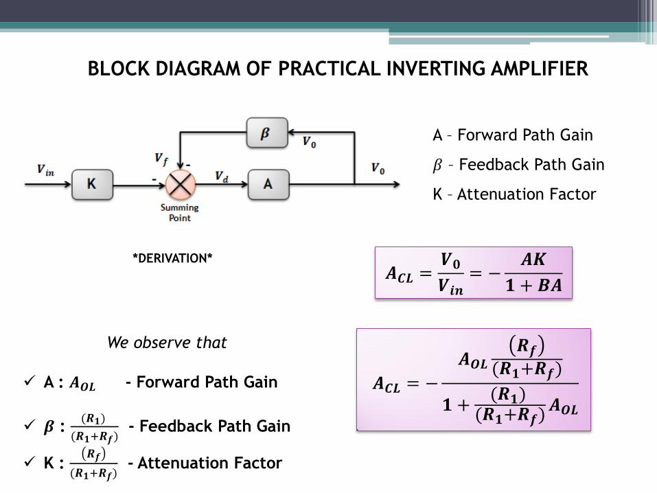
BLOCK DIAGRAM OF PRACTICAL INVERTING AMPLIFIER
A – Forward Path Gain
𝛽 – Feedback Path Gain
K – Attenuation Factor
𝑨𝑪𝑳 =𝑽𝟎
𝑽𝒊𝒏= −
𝑨𝑲
𝟏 + 𝑩𝑨
𝑨𝑪𝑳 = −
𝑨𝑶𝑳
𝑹𝒇
(𝑹𝟏+𝑹𝒇)
𝟏 +(𝑹𝟏)
(𝑹𝟏+𝑹𝒇)𝑨𝑶𝑳
We observe that
A : 𝑨𝑶𝑳 - Forward Path Gain
𝜷 : (𝑹𝟏)
(𝑹𝟏+𝑹𝒇) - Feedback Path Gain
K : 𝑹𝒇
(𝑹𝟏+𝑹𝒇) - Attenuation Factor
*DERIVATION*
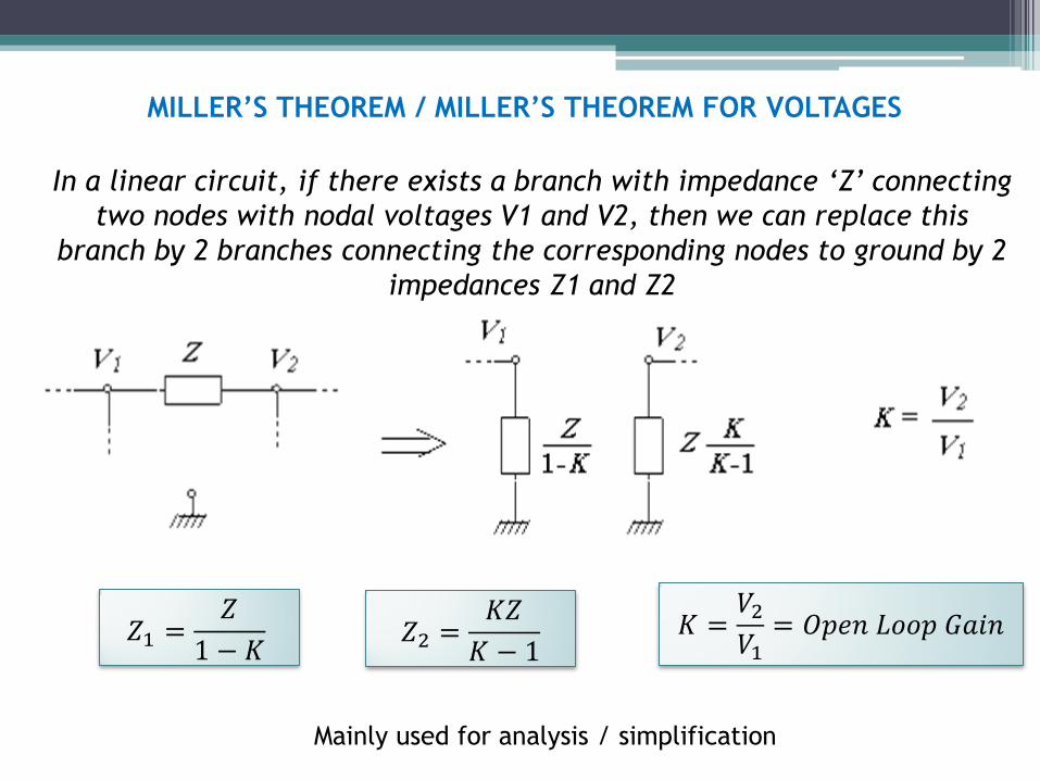
MILLER’S THEOREM / MILLER’S THEOREM FOR VOLTAGES
In a linear circuit, if there exists a branch with impedance ‘Z’ connecting
two nodes with nodal voltages V1 and V2, then we can replace this
branch by 2 branches connecting the corresponding nodes to ground by 2
impedances Z1 and Z2
Mainly used for analysis / simplification
𝑍1 =𝑍
1 − 𝐾 𝑍2 =
𝐾𝑍
𝐾 − 1 𝐾 =
𝑉2𝑉1
= 𝑂𝑝𝑒𝑛 𝐿𝑜𝑜𝑝 𝐺𝑎𝑖𝑛
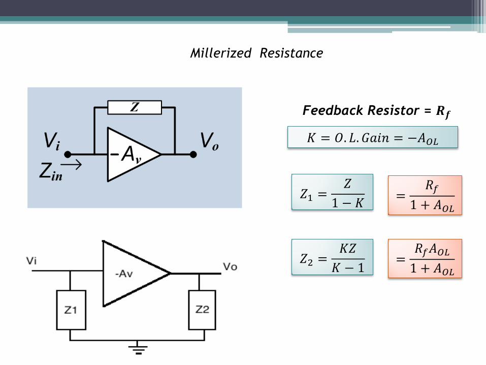
Feedback Resistor = 𝑹𝒇
𝑍1 =𝑍
1 − 𝐾
𝑍2 =𝐾𝑍
𝐾 − 1
=𝑅𝑓
1 + 𝐴𝑂𝐿
=𝑅𝑓𝐴𝑂𝐿
1 + 𝐴𝑂𝐿
Millerized Resistance
𝐾 = 𝑂. 𝐿. 𝐺𝑎𝑖𝑛 = −𝐴𝑂𝐿
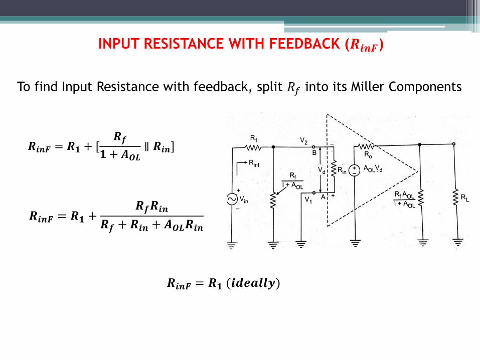
INPUT RESISTANCE WITH FEEDBACK (𝑹𝒊𝒏𝑭)
To find Input Resistance with feedback, split 𝑅𝑓 into its Miller Components
𝑹𝒊𝒏𝑭 = 𝑹𝟏 +𝑹𝒇𝑹𝒊𝒏
𝑹𝒇 + 𝑹𝒊𝒏 + 𝑨𝑶𝑳𝑹𝒊𝒏
𝑹𝒊𝒏𝑭 = 𝑹𝟏 (𝒊𝒅𝒆𝒂𝒍𝒍𝒚)
𝑹𝒊𝒏𝑭 = 𝑹𝟏 + [𝑹𝒇
𝟏 + 𝑨𝑶𝑳∥ 𝑹𝒊𝒏]
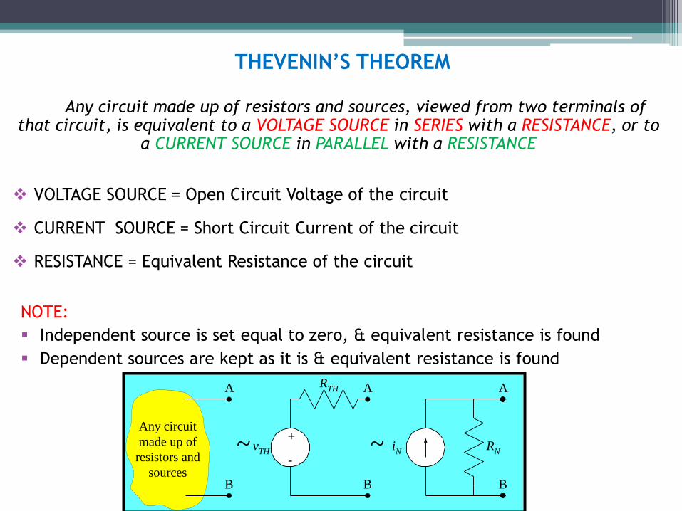
THEVENIN’S THEOREM
Any circuit made up of resistors and sources, viewed from two terminals of that circuit, is equivalent to a VOLTAGE SOURCE in SERIES with a RESISTANCE, or to
a CURRENT SOURCE in PARALLEL with a RESISTANCE
VOLTAGE SOURCE = Open Circuit Voltage of the circuit
CURRENT SOURCE = Short Circuit Current of the circuit
RESISTANCE = Equivalent Resistance of the circuit
NOTE:
Independent source is set equal to zero, & equivalent resistance is found
Dependent sources are kept as it is & equivalent resistance is found
vTH
+
-
RTH A
B
~Any circuit
made up of
resistors and
sources
A
B
A
B
~ iN
RN
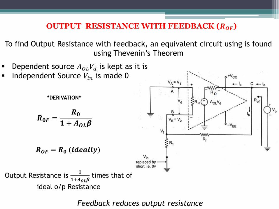
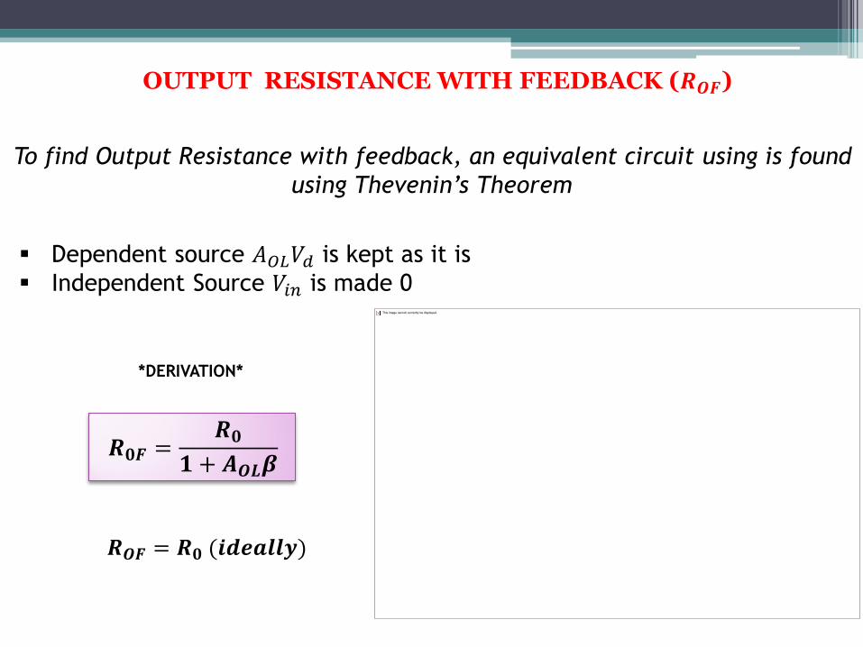
OUTPUT RESISTANCE WITH FEEDBACK (𝑹𝑶𝑭)
To find Output Resistance with feedback, an equivalent circuit using is found
using Thevenin’s Theorem
Dependent source 𝐴𝑂𝐿𝑉𝑑 is kept as it is
Independent Source 𝑉𝑖𝑛 is made 0
𝑹𝟎𝑭 =𝑹𝟎
𝟏 + 𝑨𝑶𝑳𝜷
*DERIVATION*
𝑹𝑶𝑭 = 𝑹𝟎 (𝒊𝒅𝒆𝒂𝒍𝒍𝒚)
Feedback reduces output resistance
Output Resistance is 𝟏
𝟏+𝑨𝑶𝑳𝜷 times that of
ideal o/p Resistance
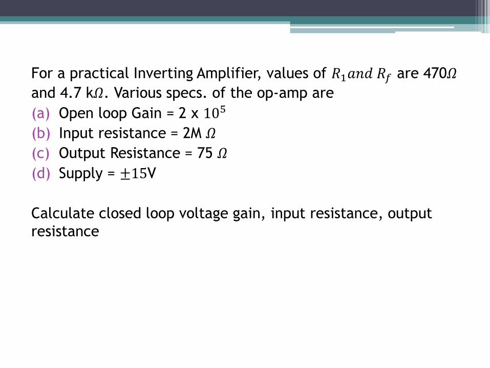
For a practical Inverting Amplifier, values of 𝑅1𝑎𝑛𝑑 𝑅𝑓 are 470𝛺
and 4.7 k𝛺. Various specs. of the op-amp are
(a) Open loop Gain = 2 x 10⁵
(b) Input resistance = 2M 𝛺
(c) Output Resistance = 75 𝛺
(d) Supply = ±15V
Calculate closed loop voltage gain, input resistance, output
resistance
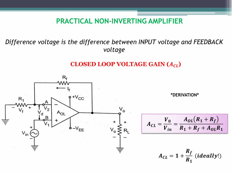
PRACTICAL NON-INVERTING AMPLIFIER
Difference voltage is the difference between INPUT voltage and FEEDBACK
voltage
*DERIVATION*
CLOSED LOOP VOLTAGE GAIN (𝑨𝑪𝑳)
𝑨𝑪𝑳 =𝑽𝟎
𝑽𝒊𝒏=
𝑨𝑶𝑳 𝑹𝟏 + 𝑹𝒇
𝑹𝟏 +𝑹𝒇 + 𝑨𝑶𝑳𝑹𝟏
𝑨𝑪𝑳 = 𝟏 +𝑹𝒇
𝑹𝟏 (𝒊𝒅𝒆𝒂𝒍𝒍𝒚!)
BLOCK DIAGRAM OF PRACTICAL NON INVERTING AMPLIFIER
A – Forward Path Gain
𝛽 – Feedback Path Gain
𝑨𝑪𝑳 =𝑽𝟎
𝑽𝒊𝒏=
𝑨
𝟏 + 𝑩𝑨
𝑨𝑪𝑳 = −𝑨𝑶𝑳
𝟏 +(𝑹𝟏)
(𝑹𝟏+𝑹𝒇)𝑨𝑶𝑳
We observe that
A : 𝑨𝑶𝑳 - Forward Path Gain
𝜷 : (𝑹𝟏)
(𝑹𝟏+𝑹𝒇) - Feedback Path Gain
*DERIVATION*
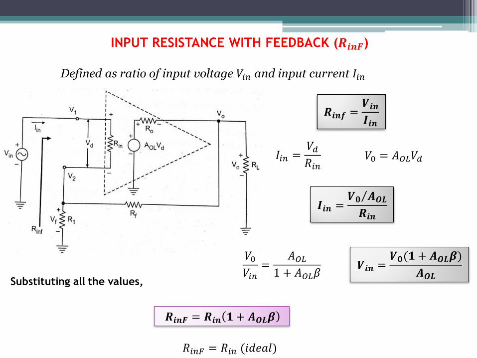
INPUT RESISTANCE WITH FEEDBACK (𝑹𝒊𝒏𝑭)
𝑹𝒊𝒏𝑭 = 𝑹𝒊𝒏 𝟏 + 𝑨𝑶𝑳𝜷
𝑅𝑖𝑛𝐹 = 𝑅𝑖𝑛 (𝑖𝑑𝑒𝑎𝑙)
𝑹𝒊𝒏𝒇 =𝑽𝒊𝒏
𝑰𝒊𝒏
𝐼𝑖𝑛 =𝑉𝑑𝑅𝑖𝑛
𝑉0 = 𝐴𝑂𝐿𝑉𝑑
𝑰𝒊𝒏 =𝑽𝟎 𝑨𝑶𝑳
𝑹𝒊𝒏
𝑉0𝑉𝑖𝑛
=𝐴𝑂𝐿
1 + 𝐴𝑂𝐿𝛽
Defined as ratio of input voltage 𝑉𝑖𝑛 and input current 𝐼𝑖𝑛
𝑽𝒊𝒏 =𝑽𝟎(𝟏 + 𝑨𝑶𝑳𝜷)
𝑨𝑶𝑳
Substituting all the values,
OUTPUT RESISTANCE WITH FEEDBACK (𝑹𝑶𝑭)
To find Output Resistance with feedback, an equivalent circuit using is found
using Thevenin’s Theorem
Dependent source 𝐴𝑂𝐿𝑉𝑑 is kept as it is
Independent Source 𝑉𝑖𝑛 is made 0
𝑹𝟎𝑭 =𝑹𝟎
𝟏 + 𝑨𝑶𝑳𝜷
*DERIVATION*
𝑹𝑶𝑭 = 𝑹𝟎 (𝒊𝒅𝒆𝒂𝒍𝒍𝒚)
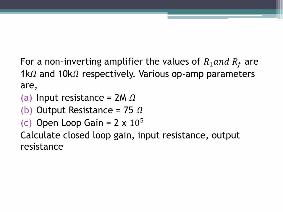
For a non-inverting amplifier the values of 𝑅1𝑎𝑛𝑑 𝑅𝑓 are
1k𝛺 and 10k𝛺 respectively. Various op-amp parameters
are,
(a) Input resistance = 2M 𝛺
(b) Output Resistance = 75 𝛺
(c) Open Loop Gain = 2 x 10⁵
Calculate closed loop gain, input resistance, output
resistance
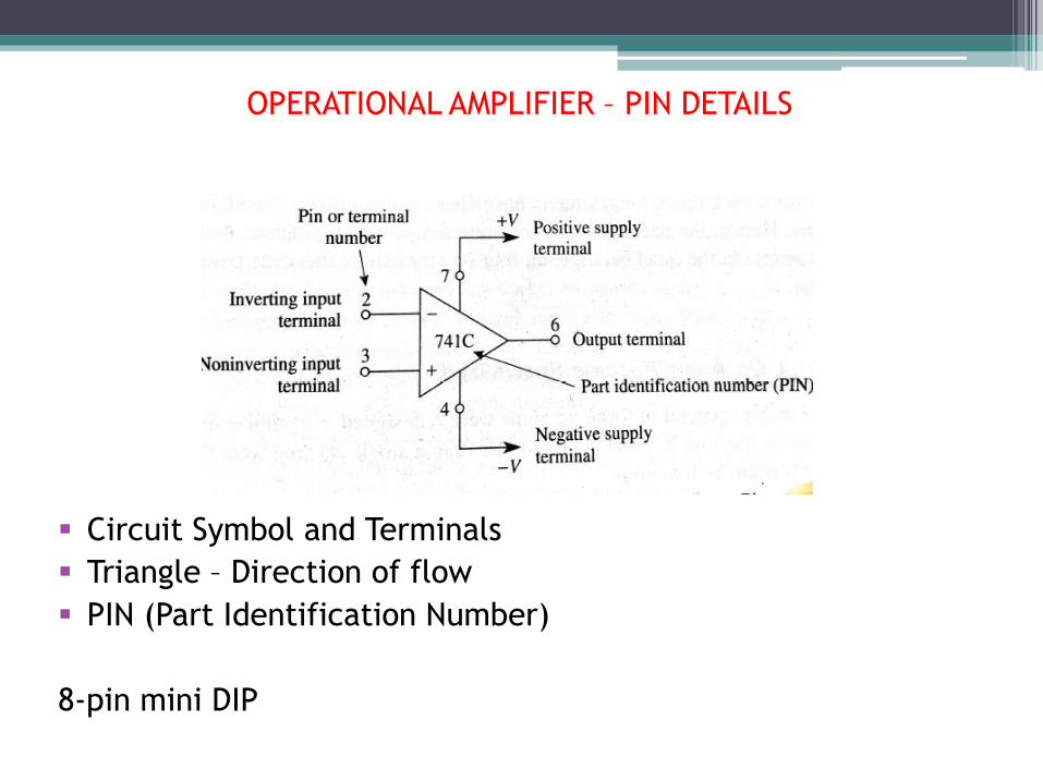
OPERATIONAL AMPLIFIER – PIN DETAILS
Circuit Symbol and Terminals
Triangle – Direction of flow
PIN (Part Identification Number)
8-pin mini DIP
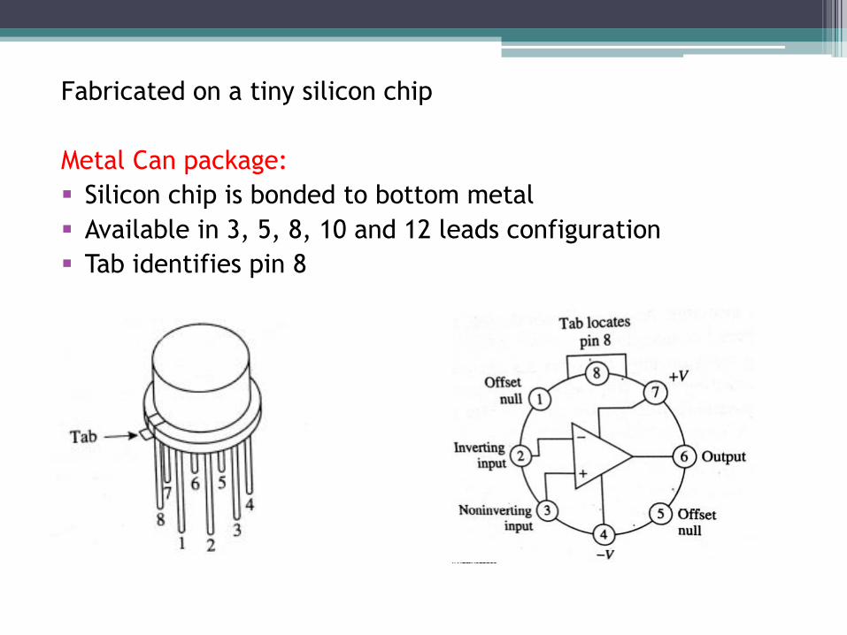
Fabricated on a tiny silicon chip
Metal Can package:
Silicon chip is bonded to bottom metal
Available in 3, 5, 8, 10 and 12 leads configuration
Tab identifies pin 8
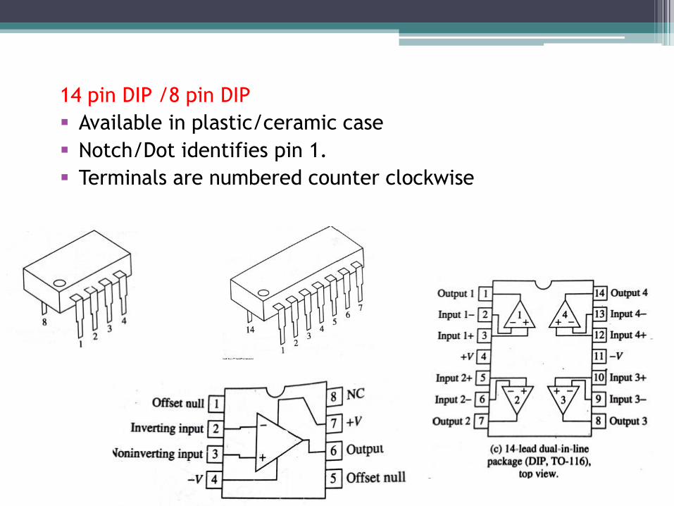
14 pin DIP /8 pin DIP
Available in plastic/ceramic case
Notch/Dot identifies pin 1.
Terminals are numbered counter clockwise
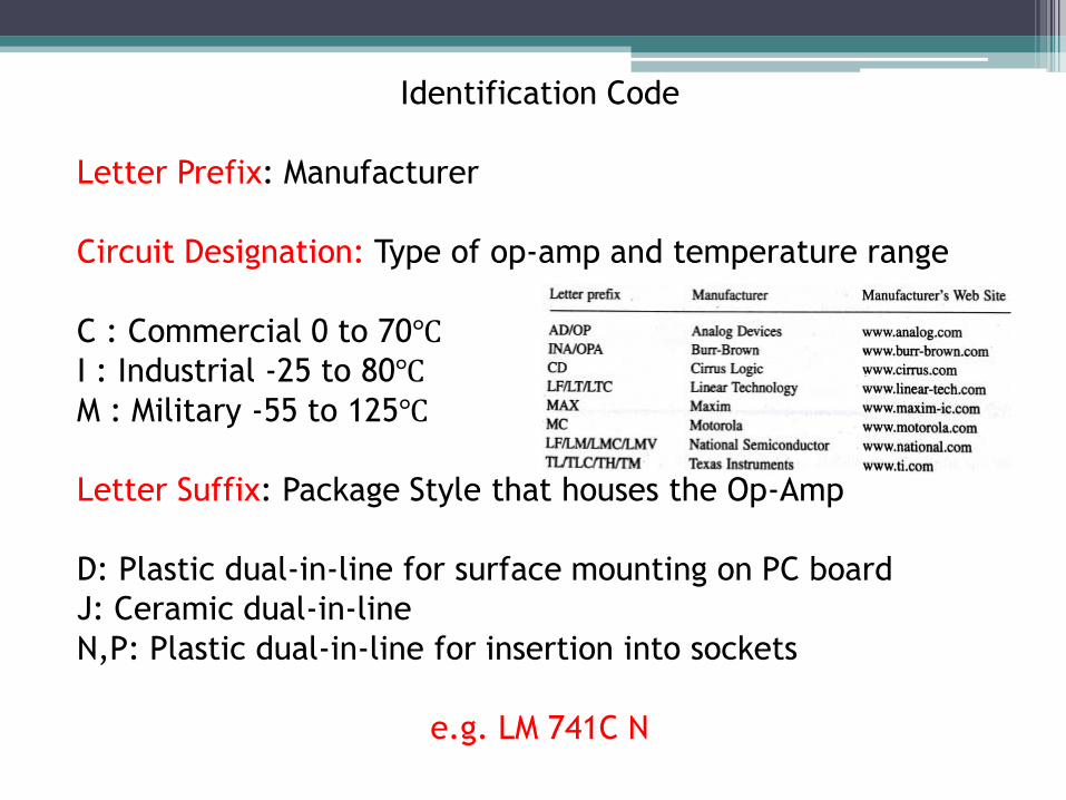
Identification Code
Letter Prefix: Manufacturer
Circuit Designation: Type of op-amp and temperature range
C : Commercial 0 to 70℃
I : Industrial -25 to 80℃
M : Military -55 to 125℃
Letter Suffix: Package Style that houses the Op-Amp
D: Plastic dual-in-line for surface mounting on PC board
J: Ceramic dual-in-line
N,P: Plastic dual-in-line for insertion into sockets
e.g. LM 741C N