Embed Size (px)
Citation preview

Memory Impedance in TiO2 basedMetal-Insulator-Metal DevicesLi Qingjiang1,2, Ali Khiat2, Iulia Salaoru2, Christos Papavassiliou3, Xu Hui1 & Themistoklis Prodromakis2,3
1College of Electronic Science and Engineering, National University of Defense Technology, Changsha 410073, P. R. China,2Nano Research Group, School of Electronics and Computer Science, University of Southampton, Southampton SO17 1BJ, UK,3Department of Electrical and Electronic Engineering, Imperial College London, London SW7 2AZ, UK.
Large attention has recently been given to a novel technology named memristor, for having the potential ofbecoming the new electronic device standard. Yet, its manifestation as the fourth missing element is rathercontroversial among scientists. Here we demonstrate that TiO2-based metal-insulator-metal devices aremore than just a memory-resistor. They possess resistive, capacitive and inductive components that canconcurrently be programmed; essentially exhibiting a convolution of memristive, memcapacitive andmeminductive effects. We show how non-zero crossing current-voltage hysteresis loops can appear and weexperimentally demonstrate their frequency response as memcapacitive and meminductive effects becomedominant.
Classical circuit theory is founded on the axiomatic definition of three fundamental circuit elements: theresistor by Ohm1, the inductor by Faraday2, and the capacitor by Volta3. These definitions however areonly static descriptions of the instantaneous values of the corresponding variables, despite the fact that
dynamic responses have been observed well before the establishment of these definitions4. About forty years ago,Chua envisioned the concept of memory-resistors (memristors) based-upon a symmetry argument5 that imposedthe existence of a missing fundamental circuit element that provided linkage between charge and flux (FigureS1a). Whilst this argument is considered to be fair, the later generalised definition by Chua and Kang6 is of morefundamental importance as it provides a state-dependent relationship between current and voltage that broadlycaptures dynamic resistive elements7. Originally the broad generalization of ‘‘memristors’’ was conceived as a newclass of dynamical systems and as such it was referred as ‘‘memristive systems’’. To avoid confusion, we follow thelatest notation imposed by Chua, the lead author of both reports, and we refer to this class of devices as‘‘memristors’’. This is in tandem with the denomination of capacitors and inductors; practical implementationsare not explicit facsimile to the corresponding ideal definitions yet these are not called capacitive or inductivesystems.
Similarly, two new auxiliary classes of dynamical elements were coined up8 as memory-capacitors (memca-pacitors) and memory-inductors (meminductors) that establish state-dependent relationships among charge-voltage (Figure S1b) and current-flux (Figure S1c) respectively. The common property of these distinct subsets ismemory, which is attributed to inertia between the causal stimulus and the diverse range of physical mechanismsthat support the various state modalities. The signature of this inertia is a pinched hysteresis loop in the i-v, q-vand w-i domain respectively for memristors, memcapacitors and meminductors (Figures S1d,e,f); notwithstand-ing the classical definitions of resistors, capacitors and inductors that are described by single-valued functions andshould thus be considered as special cases of these broad subsets (Figure 1a).
To date, the research community has shown great interest on demonstrating exclusive solid-state implementa-tions of memristors9–11, memcapacitors12–14 and meminductors15,16; some of which are highlighted in a review byPershin and Di Ventra17. Deliberate attempts to fabricate practical cells, past HP’s work on memristors11 and thesupplementary theoretical definitions for memcapacitors and meminductors8, have strived to match the char-acteristics dictated by the ideal definitions, while reports on related phenomena that were incidentally observedwere more relaxed. There is serious contention among scientists particularly for memristors, the most exploitedsubset of devices so far is the non-zero crossing i-v characteristics of solid-state implementations which isconsidered to be contradicting the original theoretical conception18, arguing the need for revamping the existingmemristor theory; a plausible extension is to incorporate a nano-battery effect19.
In our opinion, the global definition of memristors6 is well-defined. Such phenomena simply manifest the co-existence of distinct memory modalities20, which collectively facilitate a response that inevitably differs from theclassical theoretical definition; one should be able to disentangle the individual contributions within single
OPEN
SUBJECT AREAS:ELECTRONIC DEVICES
ELECTRICAL AND ELECTRONICENGINEERING
Received28 October 2013
Accepted7 March 2014
Published31 March 2014
Correspondence andrequests for materials
should be addressed toT.P. (t.prodromakis@
soton.ac.uk)
SCIENTIFIC REPORTS | 4 : 4522 | DOI: 10.1038/srep04522 1

devices. The coexistence of parasitic effects has been observed onpractical devices for more than a century21,22, with this effect beingmore apparent when the devices’ characteristics are exploited inbroad frequency spectrums where the static parasitic contributionsare more notable. We argue that practical solid-state devices wouldexperience dynamic parasitic contributions and it is thus moreappropriate to investigate the devices’ response utterly as memoryimpedance. Figure 1a demonstrates conceptually how such a com-plex interaction emerges by the mingling of distinct memory effects,namely memristive, memcapacitive and meminductive. Particularlyin case I (III) the corresponding i-v crossing point would occurwithin the first (third) quadrant as illustrated in Figure 1b (1c),due to an additive memcapacitive (meminductive) contribution. Incase IV however, all three fundamental memory effects are expressedin a device and the i-v crossing point could either occur within thefirst or third quadrant as shown in Figure 1d, depending upon thedevice’s impedance constituent memory elements (Figure 1d inset),whose dominance is determined via the stimulus frequency.
Non-zero-crossing behaviour of TiO2 based metal-insulator-metal devicesHere, we experimentally demonstrate the coexistence of dynamicparasitic effects in the prototypical Metal-Insulator-Metal (MIM)single crossbar architecture based on a TiO21x/TiO2 functionalcore23; one of our prototypes is illustrated in the inset of Figure 2a.Multiple devices were fabricated, with the fabrication flowchart out-lined in the Methodology section. For all devices, we initially employa quasi-static 63 V voltage sweep for acquiring the characteristicpinched-hysteresis i-v loop that is the well-known memristor sig-nature24. Figure 2a shows the i-v signature of a Pt/TiO21x/TiO2/Ptcell with an active area of 5 3 5 mm2. In this case, we observed that thecrossing point occurs at 1 V, indicating the presence of some para-sitic capacitance. The influence on this parasitic capacitance wasexplored while programming the device at bipolar states (seeFigures S2a, b for programming/evaluating procedure). Figures 2band 2c demonstrate the concurrent resistive/capacitive switching ofour prototype, toggling from a high-resistive state (HRS) to a low-resistive state (LRS) and correspondingly from a high-capacitivestate (HCS) to a low-capacitive state (LCS). These experimentalresults confirm that the memristive behavior is indeed accompaniedby a memcapacitive behavior. It is worthy to point out that thecapacitance switching ratio is frequency dependent25. As demon-strated in Figure 2c, the difference between HCS and LCS is signifi-cantly larger at the lower C-V test frequency (100 KHz). Unlessotherwise stated, all C-V tests were implemented at 1 MHz, a fre-quency that is near to the RC pole of the device. Thus, the capacitiveswitching ratio is lower than that of resistance extrapolated from DC
pulses. Similar experimental results have been previously demon-strated in other ReRAM devices20,25. In this manuscript, all testeddevices were electrically characterized without employing an electro-forming step. As a result, the activation energy supplied by a single setor reset pulse is not sufficient to generate formation and rupture ofcontinuous filaments. Resistive switching events are thus not avail-able at each programming pulse, rather at multiple pulses that facil-itate a collective behavior, as demonstrated in Figures 2b and 2c.
In this particular case, the memristive/memcapacitive switchingare correlated; a phenomenon that has previously been observed inperovskite25. It is worth mentioning though that the coexistence ofmemristive and memcapacitive behaviors have also been observedon other MIM cells from the same wafer with 2 3 2 mm2 and 10 3
10 mm2 active areas. Interestingly, the programming memristanceand memcapacitance of devices of 2 3 2 mm2 active area are anti-correlated, as shown in Figure S2c, while devices with larger activeareas, i.e. 5 3 5 mm2 and 10 3 10 mm2, follow alike switching trends.Similar opposing memristor – memcapacitor programming trendshave been reported recently26, with the programming and evaluationof the two memory properties though being executed independentlyone from another. The reason for the area dependence of the rela-tionship between capacitance and resistance is argued to be due todistinct dominant conducting mechanisms. It should be noted thatthe measured data in devices with active area of 2 3 2 mm2 wasattained under bipolar switching mode, where schottky barriers atboth the top and bottom interfaces are anticipated to play a dominantrole. In this case, positive programming pulses could decrease the topinterface resistance and its related capacitance, but it would notnecessarily increase the bottom interface resistance and its relatedcapacitance due to the pulse’s saturation limit25,27. As a result, thedevice’s effective resistance will decrease due to the shunting of thetop space charge region. In turn, the total capacitance of the wholedevice will increase because its value is now dominated mainly by thebottom interface25. Similar explanations apply for negative program-ming pulses. To further explore any possible influence of the device’selectrodes on the measured capacitance, we implemented C-V testson pristine devices of varying electrode areas (2 3 2 mm2, 5 3 5 mm2,and 10 3 10 mm2). As expected, the measured initial capacitance is inproportion to the electrode areas and the capacitance per unit elec-trode area is ascertained to be Cunit 5 18 (fF/mm2). Detailed argu-ments could be found in Supplementary materials.
The experimental results shown in Figure S3 in the supplementarymaterials serve as evidence that the functional mechanism of resist-ance modulation in our MIM devices is indeed filamentary in nature.We thus argue that for the device to assume a LRS, the TiO2 core willlocally undergo substantial reduction (TiO2-x) that will support oneor multiple continuous current percolation filaments that would
Figure 1 | Classification of Memory Impedance. (a) Illustration of the three fundamental subsets of dynamic elements, with the overlapping areas
representing plausible complex memory expressions in practical devices. Non-zero crossing i-v characteristics are attributed to the coexistence of distinct
memory features; shown are distinct cases of (b) memristance and memcapacitance coexistence, (c) memristance and meminductance coexistence and
(d) coexistence of all memory attributes in a single device. It should be noted that the orange arrows in (b)–(d) indicate the direction of the crossing
points.
www.nature.com/scientificreports
SCIENTIFIC REPORTS | 4 : 4522 | DOI: 10.1038/srep04522 2
effortlessly conduct current from the top (TE) to the bottom elec-trode (BE), as demonstrated in Figure 2d. It should be noted that thefilament in TiO2 based resistive devices has a bulky conical shape,which has been experimentally demonstrated in recent studies28,29. Inthe case however that the device is programmed at HRS, this filamentwould be annihilated (or partially formed), resulting in a barrierregion (L1) among any existing percolation branch and the BE. Yuet al.30 pointed out that such a barrier would render a poor DCconduction that can be modelled as a capacitance, nonetheless theyoverlooked the fact that this is essentially an auxiliary memcapaci-tance, as theoretically denoted by Mouttet31. Depending on the polar-ity of the applied potentials, this barrier would decrease or increasethat in turn would set the corresponding static resistive and capacit-ive states. While the device is programmed at a HRS, measuredresults acquired by impedance spectroscopy would denote that thedevice could be statically modelled as a parallel combination of aresistor (R1) and a capacitor (C) in series with a small resistor (R0),as shown in Figure 2e. R0 represents all other Ohmic resistancesincluding that of the initial conducting filaments and measurementconnections, which is usually no more than 20 V overall32. Onewould argue that when a continuous filament is formed, resultinginto LRS, this barrier would diminish, rendering minimum staticvalues for both resistance and capacitance. This is indeed illustratedin Figure 2f, where the measured results on the presented Nyquistplot cluster together on the Re (Z) axis.
A series of repeated impedance measurement cycles was imple-mented on the 10 3 10 mm2 active cell with the acquired resultsshown in Figures 3a–3b (the corresponding programming- evalu-ating procedures are shown in Figures S2a, b). The 10 3 10 mm2 cellsdemonstrate a rather interesting response, as shown in Figure 3b,that directly contradicts the unipolar impedance measurements
acquired from 5 3 5 mm2 active cells. In this case, the applied stimulicause the device’s reactance to toggle between both negative andpositive values, indicating that capacitive and inductive behavioursare alternately dominating. The measured reactance values in thiscase are treated as the ‘net’ contribution of a concurrent capacitiveand inductive response. Our measured results thus indicate that afunctional-oxide based MIM capacitor of relatively large active area(in this case $ 10 3 10 mm2) can effectively support concurrently allthree memory states. The origin of this triple-state coexistence andthe distinct programming trends can possibly be explained via thefilamentary formation/annihilation that occurs within the active coreof our prototypes due to a redox mechanism of TiO2. In HRS, largeresistive states would ascertain large tunnelling gaps (L1) between thedevice’s electrodes, and thus should introduce a significant capacitiveeffect. A larger active area, as in the case of our 10 3 10 mm2 pro-totype, in principle allows percolation channels to occur over largervolumes, essentially facilitating the formation of winding conductivepaths that will inevitably introduce a notable effective inductance.But in HRS, the filaments density and path tortuosity are limited, andthus the capacitive effects are dominant. In contrast, the CF is fullyshorting TE and BE in LRS, which would minimise the capacitiveeffect, while introduce the dominant inductive effect from a numberof winding filaments as shown in Figure 3d. This is also verified inFigures S2c–S2e, which clearly demonstrated that the conductivity ofLRS is correlated with the cell size.
Frequency response of i-v characteristicsSo far, all non-zero-crossing behaviours have been observed byemploying sweeping potentials19 of static frequency. In order toprove our hypothesis that ReRAM cells concurrently supportmemristive, memcapacitive and meminductive components, we
Figure 2 | Measured features of practical TiO2-based MIM devices. (a) Measured i-v characteristics showing a non-zero-crossing behaviour. Inset:
Optical microscope image of a prototype cell with an active area of 5 3 5 mm2. (b) Resistance and (c) capacitance programming occurs concurrently after
pulsing the device. The capacitance values shown by solid cycles were measured at 1 MHz, while dash cycles represent results at 100 KHz. (d) Schematic of
DC conduction processes inside a 5 3 5 mm2 active cell in HRS. As the ruptured distance L1 is relatively large, the tunnelling from the bottom electrode to
the ruptured CF would block the DC conduction processes25, which would introduce larger capacitive effects. (e) Impedance spectrum of a 5 3 5 mm2
active cell in HRS, accomplished via a 10 mV AC signal (10 KHz–10 MHz, DC biasing point is 0 V). Inset: schematic of the equivalent circuit. The
semicircle suggests the active cell could be modelled as a parallel of a resistor and a capacitor. (f) Impedance spectrum of the same active cell in LRS
(1.8 KV). Inset: Schematic of DC conduction processes in LRS. After programming, a continuous CF is formed between TE and BE.
www.nature.com/scientificreports
SCIENTIFIC REPORTS | 4 : 4522 | DOI: 10.1038/srep04522 3

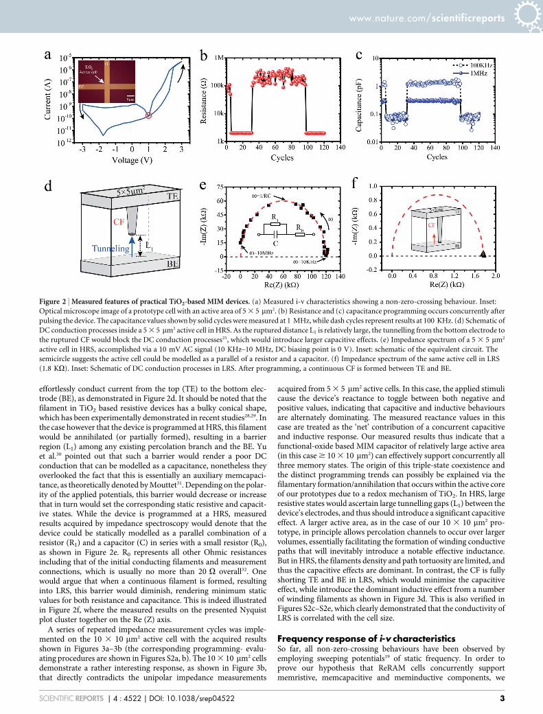
employed a sinusoidal stimulus of fixed voltage range at distincttesting frequencies. This approach allowed us to evaluate the effecton the i-v characteristics of the device under test and the shifting ofthe crossing point due to the dominance of the distinct memorycomponents at distinct frequencies, as illustrated in Figures 1b, c,d. To ensure that we do not encounter any erroneous parasitic effectswhile evaluating the characteristics of single devices, we optimisedour instrumentation setup and limited the measuring frequencyspectrum up to 1 MHz. This setup was also benchmarked whilemeasuring known SMD (Surface-mount device) components(Figure S4) that up to 1 MHz showed no significant parasitic effects.It should also be noted that to preserve devices from any hard-break-down as well as minimising the effect of any switching thresholdsasymmetry, at any single frequency point, only one sinusoidal periodwas applied from a Tektronix arbitrary function generator (AFG-3102).
Figure 4 depicts measured i-v characteristics of our 10 3 10 mm2
prototypes as the stimulus frequency ranged from 1 Hz to 1 MHz.Specifically, in the inset of Figure 4a, a small offset (40 mV) isobserved at f 5 1 Hz indicating the existence of a nanobattery19
(Vemf), as the influence of parasitic effects could be neglected at suchlow frequency. By increasing the stimulus frequency to 100 Hz, weobserve the shrinking of the area encountered within the right i-vlobe along with a slight increase in the crossing point offset, respect-ively captured in Figures 4g and 4h. The influence of a memcapaci-tive response starts to appear in Figure 4c, as the stimulus frequencyis further increased at f 5 20 KHz. The crossing i-v point is nowclearly displaced to the first quadrant, while the hysteresis loop opensup from a lissajous towards a circular form, a characteristic of mem-capacitance (Figure S1g) that becomes even more apparent at f 5
100 KHz (Figure 4d). Interestingly, further increasing the stimulusfrequency causes the crossing i-v point to drift towards the thirdquadrant, as predicted theoretically (Figure 1d) and shown hereexperimentally in Figures 4e and 4f. It is worthy to point out that
there is a step in the i-v curves in Figures 4d and 4e. We argue thisbehaviour being similar to the steps observed on the i-v character-istics of some classes of diodes that include high internal field regions,and are subject to local breakdown, such as tunnel diodes and siliconcontrolled rectifiers. In the vicinity of the breakdown such devicescan exhibit a local negative differential resistance without violatingpassivity. When the i-v characteristics of this class of devices aretraced in conductance mode (source v from a small source imped-ance, measure i) or in impedance mode (source i from a small sourceadmittance, measure v) without any special precaution to overcom-pensate the device’s negative resistance, steps could be observed asillustrated in Figures 4d and 4e. A plausible form of i-v characteristicthat can give rise to the observed step has been annotated in green onFigure 4d.
Overall, the exhibited hysteresis of our prototypes is large for lowfrequencies where the memristive component is dominant, and asfrequency increases it reduces (as anticipated by the memristor the-ory), increases (as memcapacitive effects come into play) and thenagain reduces; as depicted in Figure 4i. At the same time, the crossingi-v point origins at 0 V denotes an almost purely passive componentat low frequencies, with capacitive (inductive) components adding apositive (negative) offset at frequencies where the correspondingeffects are more dominant as depicted in Figure 4g. Our experimentalresults were closely fitted with an equivalent circuit model (inset ofFigure 4g) comprising a parallel combination of a memristor andmemcapacitor that are serially connected to a meminductor and ananobattery (detailed simulated methods and parameters can befound in Supplementary Materials). The areas bordered by thepinched hysteresis i-v loops were calculated as reported prev-iously33,34. Figure 4h depicts the changes of left and right lobes’ areas.It is clear that at frequencies below 100 Hz, the memristive effect wasdominant, thus area of right lobes dropped; Considering the migra-tion of crossing point to the first quadrant, the area of left lobe keptalmost the same. Then at frequencies between 100 Hz to 200 KHz,
Figure 3 | Impedance Features of a ReRAM cell with active area of 10 3 10 mm2. (a) Resistance changes in repeat measurement cycles at room
temperature and (b) corresponding reactance trend, evaluated at 1 MHz. Schematic illustrations of conceptual conducting filaments, formed in a (c) 5 3
5 mm2 and (d) 10 3 10 mm2 active cells. The larger the active layer’s volume, the higher the probability of observing an inductive percolating channel due
to reduced TiO2 areas forming windings.
www.nature.com/scientificreports
SCIENTIFIC REPORTS | 4 : 4522 | DOI: 10.1038/srep04522 4
memcapacitive effect was dominant, area of left lobes thus increasedsharply; In case of right lobes, the area increased initially (100 Hz–1 KHz), but then went down as a result of the crossing point migra-tion. Finally, meminductive effect became dominant above 200 KHzand the crossing point started to drift oppositely. Thus, the area ofright lobes grew up whilst an opposite trend occurred for the leftlobes. Figure 4i depicts the sum and normalised difference of thelobes’ areas at distinct frequencies. It can be observed that at frequen-cies below 10 KHz, the right lobe hysteresis outweighs the left one. Incontrast, an opposite ratio polarity could be obtained when memca-pacitive effect is dominant (10 KHz to 700 KHz), while meminduc-tive would invert the polarity again at even higher frequencies (above1 MHz).
SummaryIn this work we presented experimental evidence that TiO2-basedMIM devices, commonly known as memristors, exhibit concurrentlymemristance, memcapacitance and meminductance. We showedthat these components are concurrently modulated under voltagebiasing and we have identified that meminductance is more apparentfor devices of large active areas. We also demonstrated that the fre-quency response of the devices’ pinched-hysteresis i-v does not fol-low the classical signature of memristors, and it is a manifestation ofall three memory components. We believe that these features can beparticularly useful in developing adaptive circuits that operate inradio-frequencies35, while they open up the possibility of establishing
self-resonating nanoscale components that could find applications incellular neural networks and neuromorphic implementations36.
Methods summaryFabrication of TiO2 based active cells. In this process flow, we used thermaloxidation to grow 200 nm thick SiO2 on 40 silicon wafer and we employed opticallithography method to pattern the Bottom Electrodes (BE), Top Electrodes (TE) andthe TiO2 active material. E-beam evaporation was employed to deposit 5 nm adhesivelayer and 30 nm Pt layer as BE and 30 nm thick Pt as TE, followed by lift-off processto define the patterns. For TiO2, sputtering at 300 Watts and 2 min wet etching, in1550/HF: H2O solution, were performed. The design allows having Pt/TiO21x/TiO2/Pt ReRAM structures in cross-bars and standalone configurations.
Electrical measurements. Electrical measurements for active cells on wafer wereperformed utilising a low-noise Keithley 4200 semiconductor characteristics systemcombined with a probe station (Wentworth AVT 702). The i-v characteristics werefirstly obtained via sweeping voltages, following distinct sequences for bipolar andunipolar resistive switching. Then, impedance spectroscopies were tested biasing asmall 10 mV AC signal (DC bias is 0 V) with frequencies sweeping from 10 KHz to10 MHz. To measure the changing trends of impedance, a series programming (5 Vfor SET, and 25 V for RESET) pulses were applied across active cells with a followed0.5 V pulse to read resistance values. In all measurements, pulse widths were set to10 ms. All reactance measurements were implemented via C-V tests by employing30 mV 1 MHz AC signals (DC bias is 0.5 V). Specifically, the measuring option fordevices with active areas of 2 3 2 mm2 and 5 3 5 mm2 was set to the parallelcapacitance and conductance (Cp-Gp), while for devices with active area of 10 3
10 mm2, the measuring option was set to complex impedance (Z-Theta).
1. Ohm, G. S. Die Galvanische Kette, Mathematisch Bearbeitet (Riemann, Berlin,1827).
Figure 4 | Frequency Responses of pinched hysteresis loops for packaged diced dies. The schematics of packaged diced dies and measured method are
illustrated in Fig. S4a and b. (a)–(f) Measured i-v curves of the same device measured at frequencies from 1 Hz to 1 MHz. It should be noted that the green
dashed line in (d) depicts a plausible form of i-v characteristic that can give rise to the observed step in (d) and (e). (g) Measured and simulated
displacement of crossing points with increasing frequencies; inset depicts an equivalent circuit model (all model parameters can be found in Table S1).
(h) Measured areas bordered by left (L) and right (R) lobes of the frequency-dependent i-v characteristics. (i) Sum and normalised difference of the
hysteresis exhibited in the i-v characteristics at distinct frequencies.
www.nature.com/scientificreports
SCIENTIFIC REPORTS | 4 : 4522 | DOI: 10.1038/srep04522 5

2. Faraday, M. Experimental researches in electricity. Phil. Trans. R. Soc. Lond. 122,163–194 (1832).
3. Volta, A. Del Modo di Render Sensibilissima la piu Debole Elettricita sia Naturale,sia Artificiale. Phil. Trans. R. Soc. Lond. 72, 237–xxxiii. (1782).
4. Prodromakis, T., Toumazou, C. & Chua, L. Two centuries of memristors. Nat.Mater. 11, 478–481 (2012).
5. Chua, L. Memristor-The missing circuit element. IEEE Trans. Circuit Theory 18,507–519 (1971).
6. Chua, L. O. & Kang, S. M. Memristive devices and systems. Proc. IEEE 64, 209–223(2009).
7. Chua, L. Resistance switching memories are memristors. Appl. Phys. A 102,765–783 (2011).
8. Di Ventra, M., Pershin, Y. V. & Chua, L. O. Circuit Elements With Memory:Memristors, Memcapacitors, and Meminductors. Proc. IEEE 97, 1717–1724(2009).
9. Waser, R. & Aono, M. Nanoionics-based resistive switching memories. Nat.Mater. 6, 833–840 (2007).
10. Lu, W. & Lieber, C. M. Nanoelectronics from the bottom up. Nat. Mater. 6,841–850 (2007).
11. Strukov, D. B. et al. The missing memristor found. Nature 453, 80–83 (2008).12. Partensky, M. B. The elastic capacitor and its unusual properties. Arxiv preprint
physics/0208048 (2002).13. Kim, Y. et al. Ultralarge capacitance–voltage hysteresis and charge retention
characteristics in metal oxide semiconductor structure containing nanocrystalsdeposited by ion-beam-assisted electron beam deposition. Appl. Phys. Lett. 78,934 (2001).
14. Lee, P. F. et al. Memory effect and retention property of Ge nanocrystal embeddedHf-aluminate high- kgate dielectric. Nanotechnology 17, 1202–1206 (2006).
15. Matsuo, T., Okumura, K. & Kishima, A. Analysis of a hysteretic circuit containingan iron-cored inductor and a semiconductor switch. IEE Proc Circ Dev Syst 146,176–183 (1999).
16. Shevchenko, S. N. et al. Resonant excitations of single and two-qubit systemscoupled to a tank circuit. Phys. Rev. B 78, 174527 (2008).
17. Pershin, Y. V. & Di Ventra, M. Memory effects in complex materials andnanoscale systems. Adv. Phys. 60, 145–227 (2011).
18. Biolek, D., Biolek, Z. & BIOLKOVA, V. Pinched hysteretic loops of idealmemristors, memcapacitors and meminductors must be ‘self-crossing’. Electron.Lett. 47, 1385–1387 (2011).
19. Valov, I. et al. Nanobatteries in redox-based resistive switches require extension ofmemristor theory. Nat. Commun. 4, 1771–9 (2013).
20. Di Ventra, M. & Pershin, Y. V. Memory materials: a unifying description. Mater.Today 14, 584–591 (2011).
21. Maxwell, J. C. A treatise on electricity and magnetism (Clarendon, London, 1873).22. Kennelly, A. E. Impedance. Trans. AIEE. 10, 172–232 (1893).23. Salaoru, I., Prodromakis, T., Khiat, A. & Toumazou, C. Resistive switching of
oxygen enhanced TiO2 thin-film devices. Appl. Phys. Lett. 102, 013506 (2013).24. Joglekar, Y. & Wolf, S. The elusive memristor: signatures in basic electrical
circuits. Arxiv preprint arXiv:0807.3994 (2008).25. Liu, S., Wu, N., Ignatiev, A. & Li, J. Electric-pulse-induced capacitance change
effect in perovskite oxide thin films. J. Appl. Phys. 100, 056101 (2006).26. Yan, Z. B. & Liu, J. M. Coexistence of high performance resistance and capacitance
memory based on multilayered metal-oxide structures. Sci. Rep. 3, 02482 (2013).27. Chen, X., Wu, N. J., Strozier, J. & Ignatiev, A. Direct resistance profile for an
electrical pulse induced resistance change device. Appl. Phys. Lett. 87, 2139843(2005).
28. Kwon, D.-H. et al. Atomic structure of conducting nanofilaments in TiO2 resistiveswitching memory. Nature Nanotech 5, 148–153 (2010).
29. Kim, K. M., Jeong, D. S. & Hwang, C. S. Nanofilamentary resistive switching inbinary oxide system; a review on the present status and outlook. Nanotechnology22, 254002 (2011).
30. Yu, S., Jeyasingh, R., Wu, Y. & Philip Wong, H. S. AC conductance measurementand analysis of the conduction processes in HfOx based resistive switchingmemory. Appl. Phys. Lett. 99, 232105–232105 (2011).
31. Mouttet, B. A Memadmittance Systems Model for Thin Film Memory Materials.Arxiv preprint arXiv:1003.2842 (2010).
32. Lee, M. H. et al. Study on the electrical conduction mechanism of bipolar resistiveswitching TiO2 thin films using impedance spectroscopy. Appl. Phys. Lett. 96,152909 (2010).
33. Biolek, Z., Biolek, D. & BIOLKOVA, V. Analytical Computation of the Area ofPinched Hysteresis Loops of Ideal Mem-Elements. Radioengineering 22, 132–135(2013).
34. Biolek, D., Biolek, Z., Biolkova, V. & Kolka, Z. Computing Areas of PinchedHysteresis Loops of Mem-Systems in OrCAD PSPICE. Appl. Mech. Mater. 278,1081–1090 (2012).
35. Driscoll, T. et al. Memristive adaptive filters. Appl. Phys. Lett. 97, 093502–093503(2010).
36. Pickett, M. D., Medeiros-Ribeiro, G. & Williams, R. S. A scalable neuristor builtwith Mott memristors. Nat. mater. 12, 114–117 (2013).
AcknowledgmentsWe acknowledge the financial support of the NSFC 61171017, CHIST-ERA ERA-Net, andEPSRC EP/J00801X/1, EP/K017829/1.
Author contributionsL.Q., C.P., I.S., A.K., T.P. and X.H. conceived the experiments. A.K. and T.P. fabricated thesamples. L.Q. and I.S. performed the electrical characterization of the samples. L.Q.performed all simulations. All authors contributed in the analysis of the results and inwriting the manuscript.
Additional informationSupplementary information accompanies this paper at http://www.nature.com/scientificreports
Competing financial interests: The authors declare no competing financial interests.
How to cite this article: Qingjiang, L., Khiat, A., Salaoru, I., Papavassiliou, C., Hui, X. &Prodromakis, T. Memory Impedance in TiO2 based Metal-Insulator-Metal Devices. Sci.Rep. 4, 4522; DOI:10.1038/srep04522 (2014).
This work is licensed under a Creative Commons Attribution 3.0 Unported License.The images in this article are included in the article’s Creative Commons license,unless indicated otherwise in the image credit; if the image is not included underthe Creative Commons license, users will need to obtain permission from the licenseholder in order to reproduce the image. To view a copy of this license, visithttp://creativecommons.org/licenses/by/3.0/
www.nature.com/scientificreports
SCIENTIFIC REPORTS | 4 : 4522 | DOI: 10.1038/srep04522 6

Supplementary Information
Memory Impedance in TiO2 based Metal-Insulator-Metal Devices
Li Qingjiang1,2, Ali Khiat2, Iulia Salaoru2, Christos Papavassiliou3 and Themistoklis Prodromakis2,3*
1College of Electronic Science and Engineering, National University of Defense Technology, Changsha
410073, P. R. China
2Department of Electronics and Computer Science, University of Southampton, Southampton SO17
1BJ, UK
3Department of Electrical and Electronic Engineering, Imperial College London, London SW7 2AZ, UK.
*Email: [email protected]

Figure S1 | Theoretical characteristics of memory elements at distinct frequencies. (a), (b) and (c)
Definition curves (q-ϕ, σ-ϕ and ρ-q) of three memory elements, where ∫
and
∫
. Insert: Symbols of three memory circuit elements, namely memristor,
memcapacitor and meminductor. (d), (e) and (f) Signatures of three memory elements are pinched
hysteresis loops in i-v, q-v and –i domains respectively. (g) and (h) i-v characteristics of
memcapacitor and meminductor. Compared to i-v characteristics of memristor in (d), i-v curves of
memcapacitor and meminductor would not cross the origin, while loop areas keep synchronous with
improvement of frequency.

Figure S2 | Impedance evaluating procedure and results on active cells with distinct dimensions. (a)
Set programming and impedance measurements. After a set pulse, it is followed with resistance
reading pulse, C-V measurement at 1MHz. For C-V test, based on the polarity of imaginary part,
capacitance values (imaginary is negative) and inductance values (imaginary is positive) would be
calculated respectively. (b) Reset programming and impedance measurements. It should be noted
that for bipolar resistive switching, Set programming measurement cycles would be repeated until
resistive states toggled from HRS to LRS, and then Reset programming measurement cycles were
implemented until resistance from LRS to HRS. (c) and (d) Resistance and capacitance changes in
repeated measurement cycles on cells with active area of 2×2µm2 and 5×5µm2 respectively. It is
clear that the changing trends of resistance and capacitance are opposite on devices comprising
2×2µm2 active cells, while keep synchronous on 5×5µm2 active cells. (e) Programming trends for
resistance and imaginary parts of impedance on a 10×10µm2 active cell. The changes trends of
imaginary impedance keep synchronous with that of resistance. However, due to polarities of
imaginary values, capacitive effects and inductive effects are dominant alternatively.
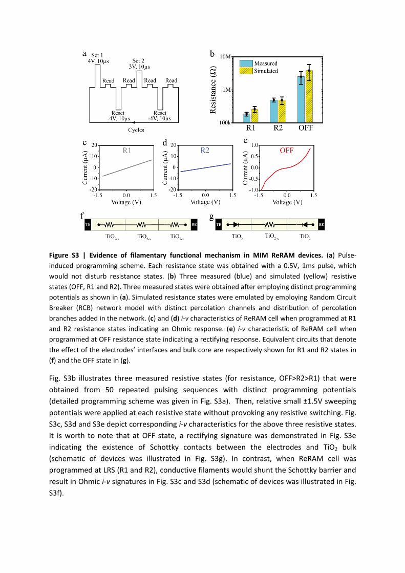
Figure S3 | Evidence of filamentary functional mechanism in MIM ReRAM devices. (a) Pulse-
induced programming scheme. Each resistance state was obtained with a 0.5V, 1ms pulse, which
would not disturb resistance states. (b) Three measured (blue) and simulated (yellow) resistive
states (OFF, R1 and R2). Three measured states were obtained after employing distinct programming
potentials as shown in (a). Simulated resistance states were emulated by employing Random Circuit
Breaker (RCB) network model with distinct percolation channels and distribution of percolation
branches added in the network. (c) and (d) i-v characteristics of ReRAM cell when programmed at R1
and R2 resistance states indicating an Ohmic response. (e) i-v characteristic of ReRAM cell when
programmed at OFF resistance state indicating a rectifying response. Equivalent circuits that denote
the effect of the electrodes’ interfaces and bulk core are respectively shown for R1 and R2 states in
(f) and the OFF state in (g).
Fig. S3b illustrates three measured resistive states (for resistance, OFF>R2>R1) that were
obtained from 50 repeated pulsing sequences with distinct programming potentials
(detailed programming scheme was given in Fig. S3a). Then, relative small ±1.5V sweeping
potentials were applied at each resistive state without provoking any resistive switching. Fig.
S3c, S3d and S3e depict corresponding i-v characteristics for the above three resistive states.
It is worth to note that at OFF state, a rectifying signature was demonstrated in Fig. S3e
indicating the existence of Schottky contacts between the electrodes and TiO2 bulk
(schematic of devices was illustrated in Fig. S3g). In contrast, when ReRAM cell was
programmed at LRS (R1 and R2), conductive filaments would shunt the Schottky barrier and
result in Ohmic i-v signatures in Fig. S3c and S3d (schematic of devices was illustrated in Fig.
S3f).

To evaluate this phenomenon, a random circuit breaker network model (RCB) was
employed. Parameters utilized in the network are set as follows: network dimension 10×10,
bulk resistance (ROFF) 10MΩ, and filamentary resistance (RON) 60KΩ. Considering SET
potential would facilitate the formation of conductive filaments, distinct number of
percolation channels and distribution of branched were added in the network, with
corresponding simulated results shown in Fig. S3b. Specifically, no percolation channel was
added in OFF state, while one and three percolation channels were added within the
network to evaluate R2 and R1 respectively. The density of percolation branches obey a
normal distribution N(70,12), while these defects were evenly distributed. Comparisons
between measured and simulated results in Fig. S3b clearly show that the experimental and
simulated results are correlated and, are therefore verifying the notion that resistance
modulation results from the formation and rupture of conductive filaments.
For each memory device in the equivalent circuit model in Fig. 4g, detailed state equations
are given as follows:
Memristor:
MEM OFF OFF ONR R R R x (1)
2/ ( ) ( ), ( ) /v ONdx dt ki t f x k R D (2)
2 10( ) 1 ((0.5 ) 0.75)f x x (3)
Memcapacitor:
, 1/ MEM ON OFF ON MEM MEMD D D D x D C (4)
dx
ki t f xdt
(5)
2 10( ) 1 ((0.5 ) 0.75)f x x (6)
Meminductor:
2
MEM ON OFF ONL L x L L
(7)
dx
ki t f xdt
(8)
2 10( ) 10* 1 ((0.5 ) 0.75)f x x (9)

Table S1 | Simulation Parameters utilized in equivalent circuit model
Stimulus Magnitude: 6V, Frequency: [1,10MHz]
Switching range
Initial state Ion mobility
Window Function
Memristor ROFF=200KΩ RON=2 KΩ
RINI=200KΩ D=10nm
µv=1e-14 f(x)=(1-((0.5-x)2+0.75)10)
Memcapacitor COFF=3pF CON=0.1pF
CINI=3pF k=1e7 f(x)= (1-((0.5-x)2+0.75)10)
Meminductor LOFF=7 µH LON=0.35 µH
LINI=0.35µH k=10 f(x)=10*(1-((0.5-x)2+0.75)10)
Nanobattery Vemf=0.04V
For simulations of the proposed equivalent circuit model, parameters settings are
demonstrated in Table S1. Considering the pulse-induced programming resistive switching
could be incomplete, parameters selected for the memcapacitor are a little larger than the
measured results in Fig. 2c (0.1pF-0.3pF). However, it should be noted that in repeated
simulation cycles, the initial states for three memory elements are not fixed, which is
different from Biolek’s models. Specifically, when biased with saturation stimulus, the
internal variable cannot return exactly the same value with pristine initial state in an
individual simulation cycle. Therefore, in this work, simulation will make use of the final
state of internal variable in each individual cycle as the updated Initial state of next
simulation cycle. By this way, the accuracy of simulation results could be improved.

Figure S4 | I-V curves measuring circuits and benchmark test employing SMD devices. (a) 24-pin
package of diced dies. Insert: a close-up of the bonded devices. (b) Schematic of i-v curves measuring
circuits. To distinguish current-voltage characteristics induced by ReRAM cells from influence of
cables or other issues, a 10KΩ SMD resistor is employed to implement benchmark test. (c) - (h) i-v
curves of comparing benchmark test at frequencies from 1Hz to 1MHz. As (c) – (g) shows, in our
optimised measuring circuit, cables would not introduce significant influence from 1Hz to 500KHz.
For measurement at 1MHz in (h), i-v curves exhibited capacitive behaviour, which however, is
insignificant and completely different from the inductive behaviour in Fig. 4 (f). Therefore, frequency
responses in Fig. 4 are definitely from our TiO2 based ReRAM active cells.

In order to verify the reactance trends in Figs. 2 and 3, we implemented C-V tests in the
frequency sweeping mode, and results were depicted as the Bode plots in Figs. S5a-b and
Figs. S5c-d, which corresponds to devices with active area of 5×5µm2 and 10×10µm2
respectively.
As demonstrated in Figs .S5a and S5b, the frequency dependent results on 5×5µm2 devices
correlate with the demonstrated equivalent circuit structure in Fig. 2, namely a parallel
combination of a memristor and a memcapacitor regardless of employed C-V test
frequencies. Specifically, within the frequency range [100KHz, 1MHz], both impedance
magnitude and phase angel (negative) possessed larger values at the initial state, and then
toggled to the lower bonds when the device was switched, which indicates the correlated
resistive/capacitive switching. In case of the device with active area of 10×10µm2, the
measured results at the initial state were similar to those on the 5×5µm2 device, though the
magnitude and angle values are slightly different. However, when the device was switched
to LRS, the phase angle increased significantly to be positive (500KHz – 1MHz) indicating of
the coexistence of capacitive and inductive effects, which verified the reactance trends in
Fig. 3b.
Figure S5 | Bode plots of devices with active area of 5×5 µm2 and 10×10µm2. (a) and (b) Impedance
magnitude and phase angle (in units of degree) change versus the frequency of C-V test on a device
with active area of 5×5µm2. (c) and (d) Impedance magnitude and phase angle (in units of degree)
change versus the frequency on a device with active area of 10×10µm2.

To explore the influence of electrode areas on the measured capacitance, we implemented
C-V tests (30mV, 1MHz) on pristine devices before any electrical characteristics
measurements to minimise the formation of defects within active cores. The measured
initial capacitance of devices with different active areas is shown in Table S2. It should be
noted that all tested devices are within the same wafer die and possess the same thickness.
Table S2 | Initial capacitive states of devices with different electrode areas
Electrode areas Initial capacitance (pF) Initial capacitance per unit area Cunit (pF/µm2)
2×2µm2 0.174 0.0435
5×5µm2 0.46 0.0184
10×10µm2 1.8 0.0180
As expected, the measured initial capacitance as shown in Table S2 is in proportion to the
electrode areas. Then the capacitance per unit electrode area (Cunit) was calculated for three
distinct device dimensions (2×2µm2, 5×5µm2, and 10×10µm2) respectively. The Cunit values of
devices with electrode area of 5×5µm2 and 10×10µm2 are quite similar, demonstrating the
uniform influence of electrode area on measured capacitance. However, the Cunit value on
2×2µm2 cell is relatively larger, indicating possible additional capacitance contributions from
the top and/or bottom interfaces on 2×2µm2 cells as argued in the main text, and also from
the disproportionately high fringing field contributions. The capacitance per electrode area
could thus be obtained based on experimental data from larger devices (5×5µm2, and
10×10µm2), namely: Cunit=18 (fF/µm2).