Embed Size (px)
Citation preview
Operational Amplifi ers
On completion of this chapter you should be able to:
1 Understand the main properties of operational amplifi ers. 2 Explain and apply the principles of operation for a number of operational amplifi er circuit
confi gurations. 3 Understand the signifi cance of the various amplifi er parameters when applied to practical
circuits. 4 Appreciate the use of operational amplifi ers for a number of practical applications.
81
1 Introduction
Operational amplifi ers (more commonly referred to simply as op amps) were originally designed to perform the mathematical operations of addition, subtraction, multiplication, division, sign changing, differentiation and integration in analogue computers and analogue simulators. Although still used to perform these mathematical functions they are also widely used in a vast range of other applications.
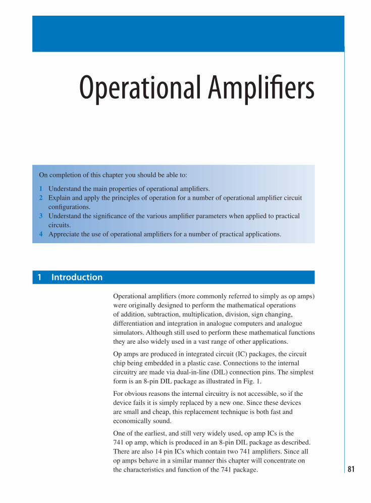
Op amps are produced in integrated circuit (IC) packages, the circuit chip being embedded in a plastic case. Connections to the internal circuitry are made via dual-in-line (DIL) connection pins. The simplest form is an 8-pin DIL package as illustrated in Fig. 1 .
For obvious reasons the internal circuitry is not accessible, so if the device fails it is simply replaced by a new one. Since these devices are small and cheap, this replacement technique is both fast and economically sound.
One of the earliest, and still very widely used, op amp ICs is the 741 op amp, which is produced in an 8-pin DIL package as described. There are also 14 pin ICs which contain two 741 amplifi ers. Since all op amps behave in a similar manner this chapter will concentrate on the characteristics and function of the 741 package.
WEBA-CH005.indd 81 5/2/2008 3:15:52 PM
82 Operational Amplifi ers
Before using an op amp in a practical situation a more detailed knowledge of the various device parameters is necessary. However, for the sake of simplicity and to avoid getting bogged down in minute detail at this stage, these parameters and their practical implications are dealt with at the end of the chapter.
2 Basic Features of an Op Amp
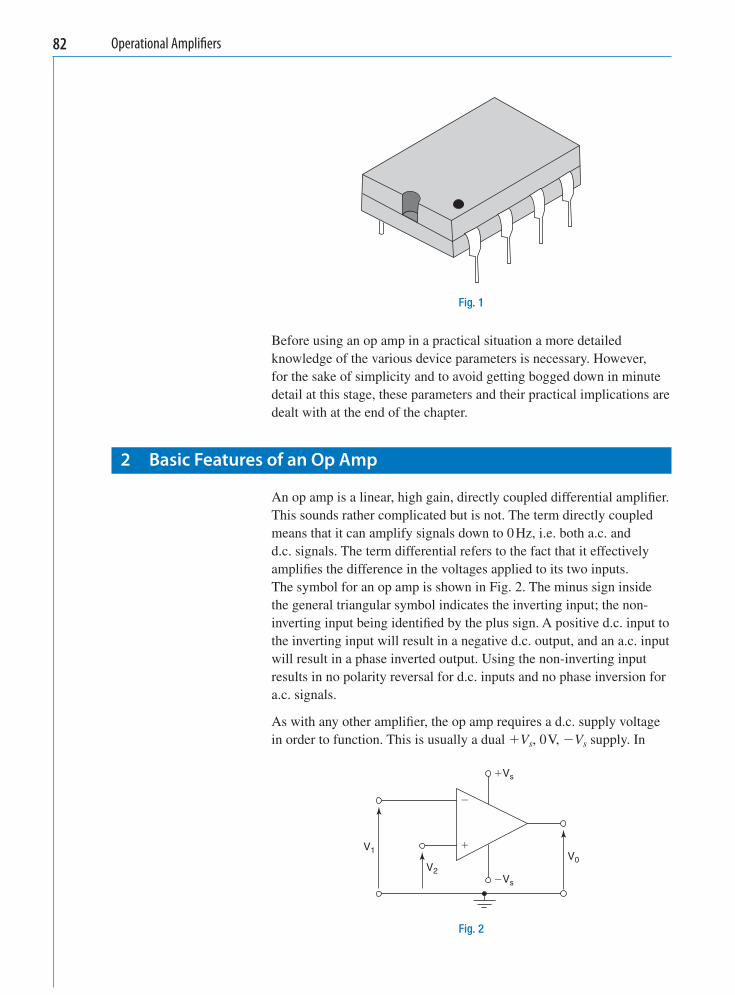
An op amp is a linear, high gain, directly coupled differential amplifi er. This sounds rather complicated but is not. The term directly coupled means that it can amplify signals down to 0 Hz, i.e. both a.c. and d.c. signals. The term differential refers to the fact that it effectively amplifi es the difference in the voltages applied to its two inputs. The symbol for an op amp is shown in Fig. 2 . The minus sign inside the general triangular symbol indicates the inverting input; the non-inverting input being identifi ed by the plus sign. A positive d.c. input to the inverting input will result in a negative d.c. output, and an a.c. input will result in a phase inverted output. Using the non-inverting input results in no polarity reversal for d.c. inputs and no phase inversion for a.c. signals.
As with any other amplifi er, the op amp requires a d.c. supply voltage in order to function. This is usually a dual V s , 0 V, Vs supply. In
Fig. 1
Fig. 2
V1V0
V2Vs
Vs
WEBA-CH005.indd 82 5/2/2008 3:15:53 PM
Operational Amplifi ers 83
Fig. 2 the V s connections are shown, but in circuit diagrams they are omitted for the sake of clarity. When using an op amp therefore, don ’ t forget to make these connections, otherwise the device will not work! As with other amplifi ers, the 0 V rail forms the common reference point for both input and output signals.
The ideal characteristics for an op amp and typical actual values for a 741 op amp are listed in Table 1.
Table 1
Characteristic Ideal Typical actual value (741)
open-loop voltage gain (A0 ) infi nite 200000 (106 dB)
input resistance infi nite 1 M
output resistance zero 75
bandwidth infi nite up to 1 MHz
common mode rejection ratio (CMMR)
infi nite 30000 (90 dB)
slew rate infi nite 0.5 V/µS
At the moment do not concern yourself with the last three items listed in the table. The explanation and signifi cance of these will be dealt with later under practical considerations. At this stage the fi rst three characteristics are the most important.
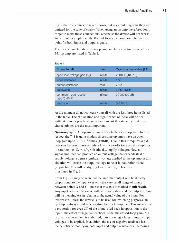
Open-loop gain All op amps have a very high open-loop gain. In this respect the 741 is quite modest since some op amps have an open-loop gain up to 30 10 6 times (150 dB). Due to this it requires a p.d. between the two inputs of only a few microvolts to cause the amplifi er to saturate, i.e. V 0 V s volt (the d.c. supply voltage). Now no signal amplifi er can produce an output voltage that exceeds its d.c. supply voltage, so any signifi cant voltage applied to the op amp in this situation will cause the output voltage to be at its saturation value (in practice this will be slightly lower than V s ). This effect is illustrated in Fig. 3 .
From Fig. 3 it may be seen that the amplifi er output will be directly proportional to the input over only the very small range of inputs between points X and Y—note that this axis is marked in microvolt . Any input outside this range will cause saturation and the output voltage will be meaningless in relation to the actual value of the input. For this reason, unless the device is to be used for switching purposes, an op amp is always used as a negative feedback amplifi er. This means that a proportion (or even all) of the input is fed back in opposition to the input. The effect of negative feedback is that the closed-loop gain (A v ) is greatly reduced and is stabilised, thus allowing a larger range of input voltages to be applied. In addition, the use of negative feedback has the benefi ts of modifying both input and output resistances, increasing
WEBA-CH005.indd 83 5/2/2008 3:15:54 PM
84 Operational Amplifi ers
the available bandwidth and reducing noise and distortion in the output signal. The reduction in closed-loop gain is easily compensated for by using more than one stage of amplifi cation if necessary.
3 The Inverting Amplifi er
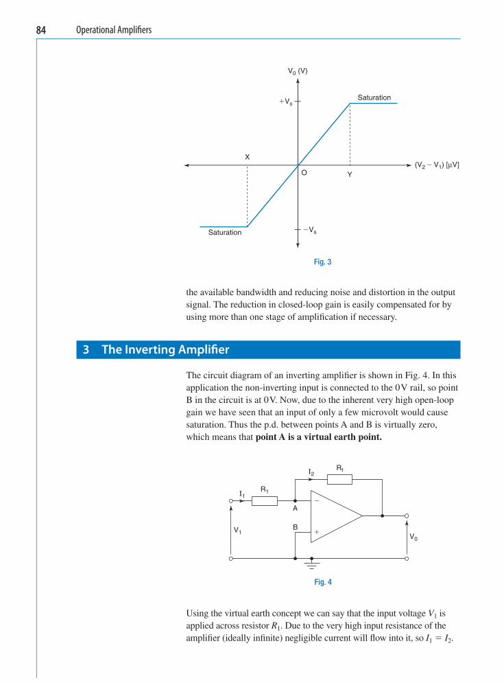
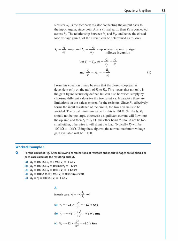
The circuit diagram of an inverting amplifi er is shown in Fig. 4 . In this application the non-inverting input is connected to the 0 V rail, so point B in the circuit is at 0 V. Now, due to the inherent very high open-loop gain we have seen that an input of only a few microvolt would cause saturation. Thus the p.d. between points A and B is virtually zero, which means that point A is a virtual earth point.
Saturation
Saturation
Vs
V0 (V)
Vs
(V2 V1) [µV]X
YO
Fig. 3
Fig. 4
V0
V1
1
2
R1
Rf
A
B
Using the virtual earth concept we can say that the input voltage V 1 is applied across resistor R 1 . Due to the very high input resistance of the amplifi er (ideally infi nite) negligible current will fl ow into it, so I 1 I 2 .
WEBA-CH005.indd 84 5/2/2008 3:15:54 PM
Operational Amplifi ers 85
Resistor R f is the feedback resistor connecting the output back to the input. Again, since point A is a virtual earth, then V 0 is connected across R f . The relationship between V 0 and V 1 , and hence the closed-loop voltage gain Av of the circuit, can be determined as follows.
IV
RI
V
R0
f1
1
12
amp, and amp where the minus sign
indictess inversion
but , so
and
I IV
R
V
R
V
VA
R
R
0
f
0v
f
1 21
1
1 1
(1)
From this equation it may be seen that the closed-loop gain is dependent only on the ratio of R f to R 1 . This means that not only is the gain fi gure accurately defi ned but can also be varied simply by choosing different values for the two resistors. In practice there are limitations on the values chosen for the resistors. Since R 1 effectively forms the input resistance of the circuit, too low a value is to be avoided. The usual minimum value for this is 10 k . Similarly, R f should not be too large, otherwise a signifi cant current will fl ow into the op amp and then I 1 I 2 . On the other hand R f should not be too small either, otherwise it will shunt the load. Typically R f will be 100 k to 1 M . Using these fi gures, the normal maximum voltage gain available will be 100.
Worked Example 1
Q For the circuit of Fig. 4 , the following combinations of resistors and input voltages are applied. For each case calculate the resulting output.
(a) R 1 100 k ; R1 1 M ; V 1 0.5 V (b) R 1 100 k ; Rf 100 k ; V 1 6.0 V (c) R 1 100 k ; Rf 10 k ; V 1 12.0 V (d) R 1 10 k ; Rf 1 M ; V 1 0.04 sin t volt (e) R 1 R f 100 k ; V 1 2.5 V
A
In each case,
V V
RR0
f 11
volt
(a) V0 0 5
00
5 06
5. .
1
1V Ans
(b)
V0 ( V 6
00
6 05
5) .
1
1Ans
(c)
V0 1
1
112
00
24
5. V Ans
WEBA-CH005.indd 85 5/2/2008 3:15:55 PM
86 Operational Amplifi ers
(d)
V t t0 0 04
00
46
4. sin sin volt
1
1Ans
(e)
V0 2 5
00
2 55
5. .
1
1V Ans
From this example it can be seen that this confi guration performs the functions of sign changing together with multiplication and division. It is worth noting at this stage that the inverting mode is used for all mathematical functions.
4 The Summing Amplifi er
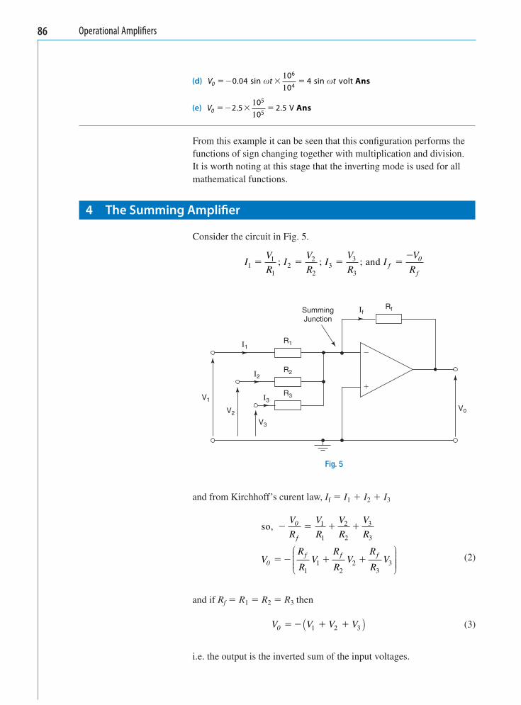
Consider the circuit in Fig. 5 .
IV
RI
V
RI
V
RI
V
Rf0
f1
1
12
2
23
3
3
; ; ; and
and from Kirchhoff ’ s curent law, I f I 1 I 2 I 3
so,
V
R
V
R
V
R
V
R
VR
RV
R
RV
R
RV
0
f
0f f f
1
1
2
2
3
3
11
22
33
⎛
⎝⎜⎜⎜⎜
⎞
⎠⎟⎟⎟⎟⎟⎟
(2)
and if R f R 1 R 2 R 3 then
V V V V0 1 2 3( )
(3)
i.e. the output is the inverted sum of the input voltages.
SummingJunction
Rff
1
V1
V0V2
V3
R1
R2
R3
2
3
Fig. 5
WEBA-CH005.indd 86 5/2/2008 3:15:56 PM
Operational Amplifi ers 87
Worked Example 2
Q For the summing amplifi er of Fig. 5 , the following combination of resistors and input voltages is applied. In each case calculate the resulting output voltage.
(a)
R R R R
V V Vf1
1
1
2 3
2 3
00
0 25 3 0 6 0
k
V; V; V
. . .
(b)
R R R R
V V Vf1
1
1 1
1
2 3
2 3
00
2 0 35 6 0
k ; M
V; V; V
. . .
A
(a) Since all the resistors are of the same value then equation (3) will apply
V V V V
V
0
0
( ) volt ( ( ) )
( )
V
1 12 3 5 3 0 6 0
7 5 3 0
4 5
. . .
. .
. Anns
(b) Using equation (2):
VRR
VRR
VRR
V0f f f
11
1
11
1
22
33
6
5
600
20
⎛
⎝⎜⎜⎜⎜
⎞
⎠⎟⎟⎟⎟⎟
volt
.11
1
1
1
00 35
00
6 0
2 3 5 6
9 5
5
6
6
. .
.
.
( )
( )
V
⎛
⎝⎜⎜⎜⎜
⎞
⎠⎟⎟⎟⎟
V0 Ans
From the last example it may be seen that as well as summation, the circuit can also multiply or divide each input by a specifi ed amount.
5 The Non-inverting Amplifi er
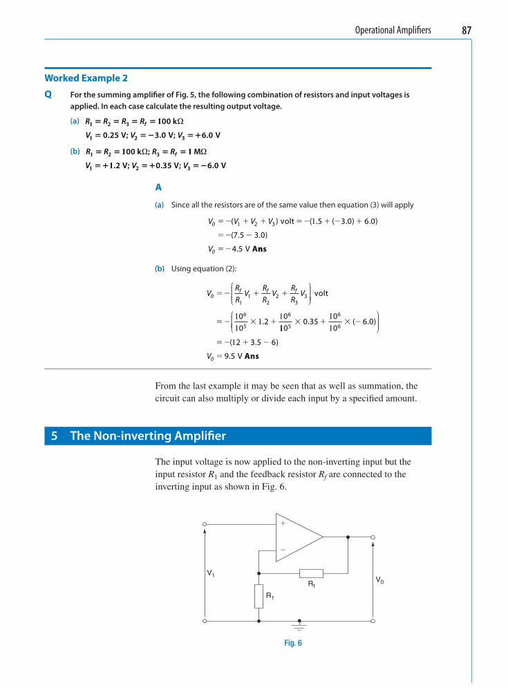
The input voltage is now applied to the non-inverting input but the input resistor R 1 and the feedback resistor R f are connected to the inverting input as shown in Fig. 6 .
Rf
V1V0
R1
Fig. 6
WEBA-CH005.indd 87 5/2/2008 3:15:57 PM
88 Operational Amplifi ers
Since zero current is assumed to fl ow into the op amp itself, and internally the two input terminals are connected by the internal resistance of the device, then no p.d. will be developed across this resistance and so the input voltage V 1 will be effectively developed across R 1 .
Resistors R f and R 1 form a potential divider between the output terminal and the 0 V rail, so the p.d. developed across R 1 will be the appropriate proportion of V 0 , thus
p.d. across
RR
R RV V
f01
1
11
V
VA
R R
R0
vf
1
1
1
A
R
Rvf
11
(4)
The main advantage of the non-inverting amplifi er is that due to the feedback arrangement the input impedance of the circuit is very high, and not just R 1 as in the previous cases.
Worked Example 3
Q The circuit of Fig. 6 has the following combination of inputs and resistors applied. In each case calculate the resulting output voltage.
(a) R f 1 M ; R 1 100 k ; V 1 0.6 V (b) R f 100 k ; R 1 1 M ; V 1 1.5 V (c) R f 1 00 k ; R 1 1 M ; V 1 5 sin t volt
A
In each case, from equation (4)
V V
RR0
f 11
1⎛
⎝⎜⎜⎜⎜
⎞
⎠⎟⎟⎟⎟⎟
(a)
V
V
0
0
0 600
0 6
6 6
6
5. .
.
11
111
⎛
⎝⎜⎜⎜⎜
⎞
⎠⎟⎟⎟⎟
V Ans
(b)
V
V
0
0
1 11
11 1 1
1
. . .
.
500
5
65
5
6
⎛
⎝⎜⎜⎜⎜
⎞
⎠⎟⎟⎟⎟
V Ans
(c)
V t t
V t
0
0
500
5
5 5
5
6 sin sin
sin
11
11 1
⎛
⎝⎜⎜⎜⎜
⎞
⎠⎟⎟⎟⎟ .
. vvolt Ans
WEBA-CH005.indd 88 5/2/2008 3:15:58 PM
Operational Amplifi ers 89
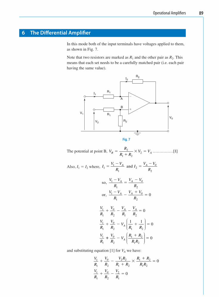
6 The Diff erential Amplifi er
In this mode both of the input terminals have voltages applied to them, as shown in Fig. 7.
Note that two resistors are marked as R 1 and the other pair as R 2 . This means that each set needs to be a carefully matched pair (i.e. each pair having the same value).
V1
R1
R1
R2
R2
V2
V0
A
B
1
2
Fig. 7
The potential at point B,
V
R
R RV VB A
2
1 22 1……………[ ]
Also, I 1 I 2 where, I
V V
RI
V V
RA A 0
11
12
2
and
so,
or,
V V
R
V V
R
V V
R
V V
R
A A 0
A A 0
1
1 2
1
1 2
0
V
R
V
R
V
R
V
R
V
R
V
RV
R R
V
R
0 A A
0A
1
1 2 1 2
1
1 2 1 2
1
1
0
1 10
⎛
⎝⎜⎜⎜⎜
⎞
⎠⎟⎟⎟⎟
V
RV
R R
R R0
A2
1 2
1 2
0⎛
⎝⎜⎜⎜⎜
⎞
⎠⎟⎟⎟⎟
and substituting equation [1] for V A we have:
V
R
V
R
V R
R R
R R
R R
V
R
V
R
V
R
0
0
1
1 2
2 2
1 2
1 2
1 2
1
1 2
2
1
0
0
WEBA-CH005.indd 89 5/2/2008 3:15:59 PM
90 Operational Amplifi ers
hence,
V
R
V
R
V
R
V V
R0
2
2
1
1
1
2 1
1
and ( ) voltV
R
RV V0 2
12 1
(5)
and if , then voltR R V V V01 2 2 1 (6)
i.e. the difference between the two inputs.
Worked Example 4
Q For the circuit of Fig. 7 the following combination of input voltages and resistors is applied. For each case calculate the resulting output voltage.
(a) R 1 R 2 100 k ; V 1 6.4 V; V 2 10.5 V (b) R 1 R 2 1 M ; V 1 2.6 V; V 2 4 V (c) R 1 100 k ; R 2 1 M ; V 1 4.9 V; V 2 3.8 V
A
(a) Since R 1 R 2 , then using equation (6)
V V V
V0
0
( ) volt
V2 0 5 6 4
41 1
1
. .
. Ans (b) Again using equation (6)
V
V0
0
(( )
V
4 2 6
6 2
) .
. Ans (c) Since R 1 R 2 then equation (5) applies
VRR
V V
V
0
0
22
6
5
00
3 8 4 9 0
11
1
11 1 1
11
( ) volt
( ) ( )
V
. . .
Ans
Note that if the supply voltage V S 10 V, then the last circuit with those values would give an invalid result since the amplifi er would saturate at an output voltage just less than 10 V.
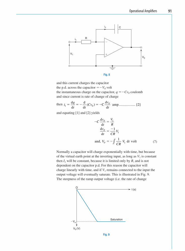
7 The Integrator
The circuit arrangement for an op amp integrator is shown in Fig. 8 , where the feedback resistor is replaced by a capacitor.
The value of I 1 at any instant, i
V
R11 1 amp....................... [ ]
WEBA-CH005.indd 90 5/2/2008 3:15:59 PM
Operational Amplifi ers 91
and this current charges the capacitor the p.d. across the capacitor V 0 volt the instantaneous charge on the capacitor, q Cv 0 coulomb and since current is rate of change of charge
then
i
q
t tCv
v
t00
1 2 d
d
d
dC
d
d amp................. [ ]( )
and equating [1] and [2] yields
Cv
t
V
Rv
t CRV
0
0
d
dd
d
1
11
and, d voltV
CRV t0
11∫
(7)
Normally a capacitor will charge exponentially with time, but because of the virtual earth point at the inverting input, as long as V 1 is constant then I 1 will be constant, because it is limited only by R , and is not dependent on the capacitor p.d. For this reason the capacitor will charge linearly with time, and if V 1 remains connected to the input the output voltage will eventually saturate. This is illustrated in Fig. 9 .The steepness of the ramp output voltage (i.e. the rate of change
V0
V1
R
Ci1
i1
Fig. 8
Ot (s)
SaturationVs
V0 (V)
Fig. 9
WEBA-CH005.indd 91 5/2/2008 3:16:00 PM
92 Operational Amplifi ers
of output) depends upon the time constant. Apart from the purely mathematical function of integration, this production of a linear ramp voltage is a very useful function that is utilised in a number of practical applications, as was mentioned in the book Further Electrical and Electronics Principles, Chapter 8. The principal advantage of using an op amp as an integrator is that the severe attenuation required for ‘ good ’ integration produced by a simple CR network can be overcome by the closed-loop gain of the amplifi er. This is achieved by having CR 1 second, e.g. C 1 µ F and R 1 M .
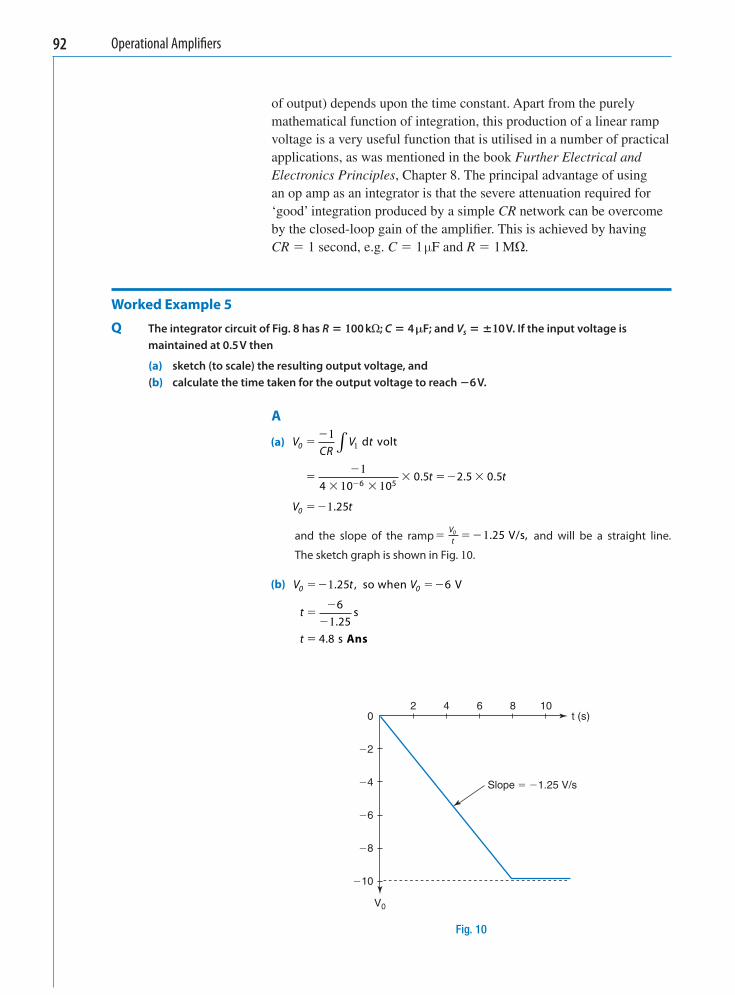
Worked Example 5
Q The integrator circuit of Fig. 8 has R 100 k; C 4 µF; and V s 10 V. If the input voltage is maintained at 0.5 V then
(a) sketch (to scale) the resulting output voltage, and (b) calculate the time taken for the output voltage to reach 6 V.
A
(a)
VCR
V t
t t
V t
0
0
1
1
1 1
1
1 d volt∫
4 0 00 5 2 5 0 5
25
6 5. . .
.
and the slope of the ramp
Vt0 1.25 V/s,
and will be a straight line.
The sketch graph is shown in Fig. 10 .
(b)
V t V
t
t
0 0
1
1
.
..
25 6
625
4 8
, so when V
s
s Ans
10
8
6
4
2
02 64 8 10
t (s)
Slope 1.25 V/s
V0
Fig. 10
WEBA-CH005.indd 92 5/2/2008 3:16:01 PM
Operational Amplifi ers 93
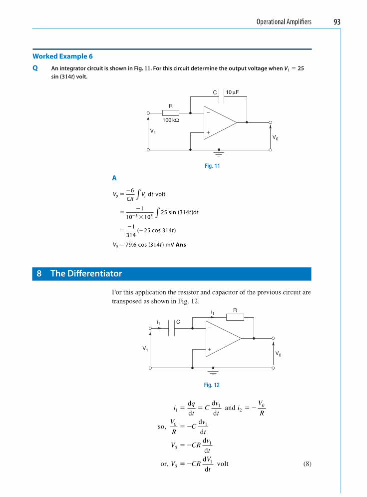
Worked Example 6
Q An integrator circuit is shown in Fig. 11 . For this circuit determine the output voltage when V 1 25 sin (314 t ) volt.
A
VCR
V t
t t
0 i
6
0 025 3 4
3 425
5 5
d volt
sin ( d
( co
∫
∫1
1 11
1
1
)
ss )
cos ( ) mV
3 4
79 6 3 4
1
1
t
V t0 . Ans
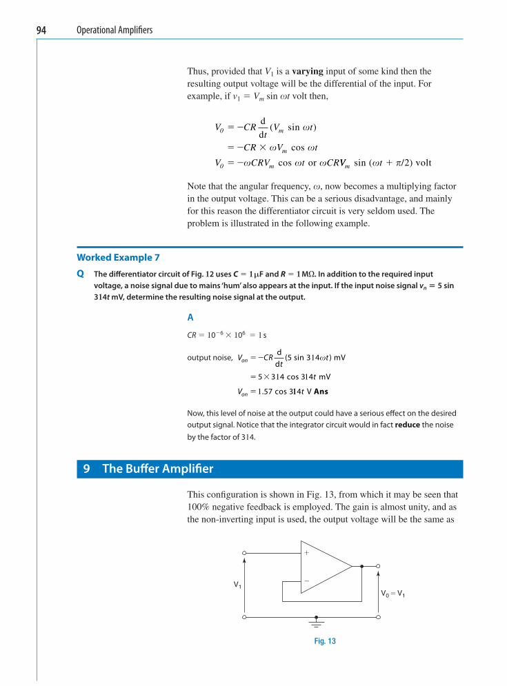
8 The Diff erentiator
For this application the resistor and capacitor of the previous circuit are transposed as shown in Fig. 12 .
iq
tC
v
ti
V
RV
RC
v
t
V CRv
t
V
0
0
0
0
11
2
1
1
d
d
d
d and
so, d
dd
d
or, CRV
t
d
d volt1
(8)
R
C 10 µF
V1V0
100 kΩ
Fig. 11
R
Ci1
i1
V0
V1
Fig. 12
WEBA-CH005.indd 93 5/2/2008 3:16:02 PM
94 Operational Amplifi ers
Thus, provided that V 1 is a varying input of some kind then the resulting output voltage will be the differential of the input. For example, if v 1 V m sin t volt then,
V CRt
V t
CR V t
V CRV t CR
0 m
m
0 m
d
d( sin )
cos
cos or
VV tm sin ( / ) volt 2
Note that the angular frequency, , now becomes a multiplying factor in the output voltage. This can be a serious disadvantage, and mainly for this reason the differentiator circuit is very seldom used. The problem is illustrated in the following example.
Worked Example 7
Q The diff erentiator circuit of Fig. 12 uses C 1 µ F and R 1 M . In addition to the required input voltage, a noise signal due to mains ‘ hum ’ also appears at the input. If the input noise signal v n 5 sin 314 t mV, determine the resulting noise signal at the output.
A
CR 10 6 10 6 1 s
output noise,
V CRt
t
t
V
on
on
dd
( sin ) mV
cos 3 4 mV
cos 3
5 3 4
5 3 4
57
1
1 1
1
. 114 V t Ans
Now, this level of noise at the output could have a serious eff ect on the desired output signal. Notice that the integrator circuit would in fact reduce the noise by the factor of 314.
9 The Buff er Amplifi er
This confi guration is shown in Fig. 13 , from which it may be seen that 100% negative feedback is employed. The gain is almost unity, and as the non-inverting input is used, the output voltage will be the same as
V1V0 V1
Fig. 13
WEBA-CH005.indd 94 5/2/2008 3:16:03 PM
Operational Amplifi ers 95
the input. If the input voltage varies then the output will follow exactly the same variations, so this arrangement is also known as a voltage follower. Due to the feedback employed the input impedance of this amplifi er is extremely high and its output impedance is very low. Its main usage is therefore as a buffer between a high impedance source and a low impedance load. These features are shared by the BJT and FET equivalents, namely the emitter follower and source follower respectively.
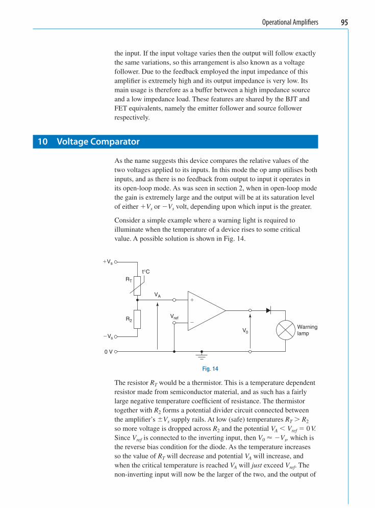
10 Voltage Comparator
As the name suggests this device compares the relative values of the two voltages applied to its inputs. In this mode the op amp utilises both inputs, and as there is no feedback from output to input it operates in its open-loop mode. As was seen in section 2, when in open-loop mode the gain is extremely large and the output will be at its saturation level of either V s or V s volt, depending upon which input is the greater.
Consider a simple example where a warning light is required to illuminate when the temperature of a device rises to some critical value. A possible solution is shown in Fig. 14 .
The resistor R T would be a thermistor. This is a temperature dependent resistor made from semiconductor material, and as such has a fairly large negative temperature coeffi cient of resistance. The thermistor together with R 2 forms a potential divider circuit connected between the amplifi er ’ s V s supply rails. At low (safe) temperatures RT R 2 so more voltage is dropped across R 2 and the potential VA V ref 0 V. Since V re f is connected to the inverting input, then V 0 V s , which is the reverse bias condition for the diode. As the temperature increases so the value of R T will decrease and potential V A will increase, and when the critical temperature is reached V A will just exceed V ref . The non-inverting input will now be the larger of the two, and the output of
Vs
Vs
0 V
V0Warninglamp
Vref
RT
R2
t°C
VA
Fig. 14
WEBA-CH005.indd 95 5/2/2008 3:16:04 PM
96 Operational Amplifi ers
the amplifi er will switch from V S to V S volt. The diode will now be forward biased and the lamp will light.
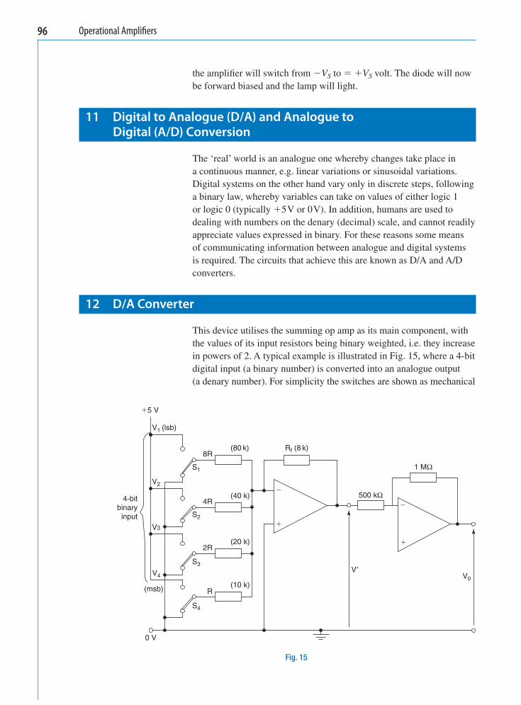
11 Digital to Analogue (D/A) and Analogue to Digital (A/D) Conversion
The ‘ real ’ world is an analogue one whereby changes take place in a continuous manner, e.g. linear variations or sinusoidal variations. Digital systems on the other hand vary only in discrete steps, following a binary law, whereby variables can take on values of either logic 1 or logic 0 (typically 5 V or 0 V). In addition, humans are used to dealing with numbers on the denary (decimal) scale, and cannot readily appreciate values expressed in binary. For these reasons some means of communicating information between analogue and digital systems is required. The circuits that achieve this are known as D/A and A/D converters.
12 D/A Converter
This device utilises the summing op amp as its main component, with the values of its input resistors being binary weighted, i.e. they increase in powers of 2. A typical example is illustrated in Fig. 15 , where a 4-bit digital input (a binary number) is converted into an analogue output(a denary number). For simplicity the switches are shown as mechanical
Fig. 15
4-bitbinaryinput
8R(80 k)
500 kΩ
1 MΩ
Rf (8 k)
(40 k)
(20 k)
(10 k)
4R
2R
R
5 V
V1 (lsb)
V0
V′
V2
V3
V4
S4
S3
S2
S1
(msb)
0 V
WEBA-CH005.indd 96 5/2/2008 3:16:04 PM
Operational Amplifi ers 97
devices, but in practice they would take the form of electronic switches. Thus each of the inputs V 1 to V 4 may be set to either 0 V or 5 V which represent the digital states of logic 0 (LOW) or logic 1 (HIGH) respectively.
The output of the summing amplifi er, V V V VR
R
R
R
R
Rf f f
8 1 4 2 2 3( R
Rf V4 ) volt
and using the actual values shown in brackets in Fig. 15
V V V V V ( ) volt0 1 0 2 0 4 0 81 2 3 4. . . .
Now, if switches S 1 and S 4 are moved to the other position, then V 1 V 4 5 V and the other two inputs will remain at 0 V. The digital input therefore represents the value 1001, which is equivalent to the denary number 9.
V ( ) volt V0 1 5 0 0 0 8 5 4 5. . .
Now, V forms the input to an inverting amplifi er with a closed-loop gain of 2, so
V0 ( ) ( ) V2 4 5 9. It is left to the reader to verify that for any combination of inputs from 0000 to 1111 will result in output voltages from 0 V to 15 V.
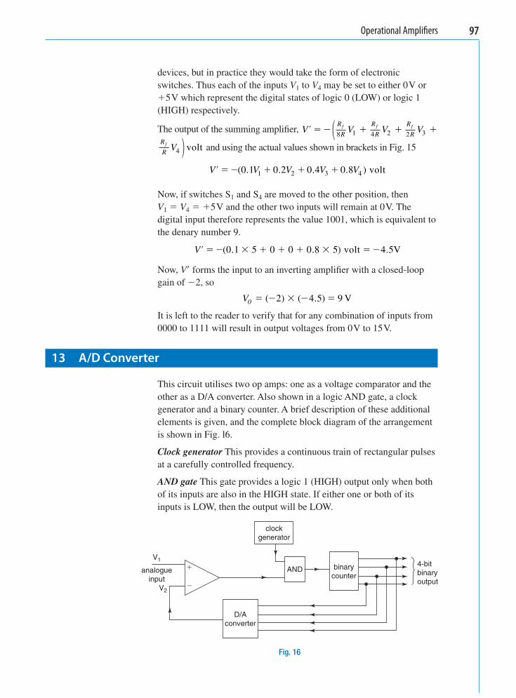
13 A/D Converter
This circuit utilises two op amps: one as a voltage comparator and the other as a D/A converter. Also shown in a logic AND gate, a clock generator and a binary counter. A brief description of these additional elements is given, and the complete block diagram of the arrangement is shown in Fig. l6 .
Clock generator This provides a continuous train of rectangular pulses at a carefully controlled frequency.
AND gate This gate provides a logic 1 (HIGH) output only when both of its inputs are also in the HIGH state. If either one or both of its inputs is LOW, then the output will be LOW.
analogue input
D/A converter
clockgenerator
AND binarycounter
V2
V1
4-bitbinary output
Fig. 16
WEBA-CH005.indd 97 5/2/2008 3:16:04 PM
98 Operational Amplifi ers
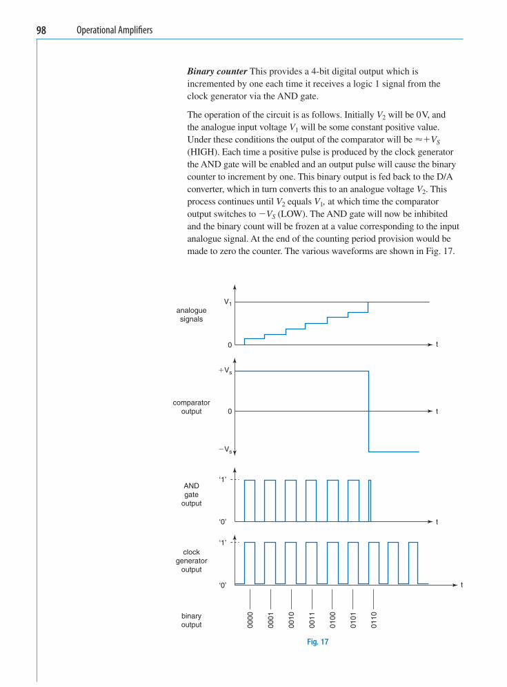
Binary counter This provides a 4-bit digital output which is incremented by one each time it receives a logic 1 signal from the clock generator via the AND gate.
The operation of the circuit is as follows. Initially V 2 will be 0 V, and the analogue input voltage V 1 will be some constant positive value. Under these conditions the output of the comparator will be V S (HIGH). Each time a positive pulse is produced by the clock generator the AND gate will be enabled and an output pulse will cause the binary counter to increment by one. This binary output is fed back to the D/A converter, which in turn converts this to an analogue voltage V 2 . This process continues until V 2 equals V 1 , at which time the comparator output switches to V S (LOW). The AND gate will now be inhibited and the binary count will be frozen at a value corresponding to the input analogue signal. At the end of the counting period provision would be made to zero the counter. The various waveforms are shown in Fig. 17 .
Fig. 17
V1
0
Vs
Vs
0
‘1’
‘0’
‘1’
‘0’
analogue signals
comparatoroutput
ANDgate
output
clockgenerator
output
binaryoutput 00
00
0001
0010
0011
0110
0101
0100
t
t
t
t
WEBA-CH005.indd 98 5/2/2008 3:16:05 PM
Operational Amplifi ers 99
14 Practical Considerations
In the foregoing descriptions of the various op amp confi gurations it has been assumed that the amplifi er was ideal. However, when using these devices in practice there are a number of non-ideal parameters that need to be considered. Where typical values are quoted in the following descriptions they refer to the 741 op amp.
Input bias current This is the average of the currents fl owing into the input terminals, the typical value being 80 nA.These (very small) currents will cause corresponding p.d.s across any resistors connected to the input terminals.
Input offset current This is the difference between the two input currents when the output voltage is zero, and will typically be 20 nA.Thus, not only is the practical amplifi er non-ideal from the standpoint that it requires input currents, but it is also non-ideal in that these currents are unequal, i.e. the two halves of the amplifi er internal circuitry are not exactly symmetrical.
Input offset voltage Ideally, when both inputs are zero (or equal) the output will be zero. In practice this is not always the case, again due to asymmetry within the internal circuitry. This effect is nulled by the use of an external potentiometer. The two ends of this potentiometer are connected to terminals on the IC package marked ‘ offset null ’ (pins 1 and 5), and the wiper is connected to the V s supply (pin 4). With both input terminals grounded the potentiometer is adjusted until the output is zero.
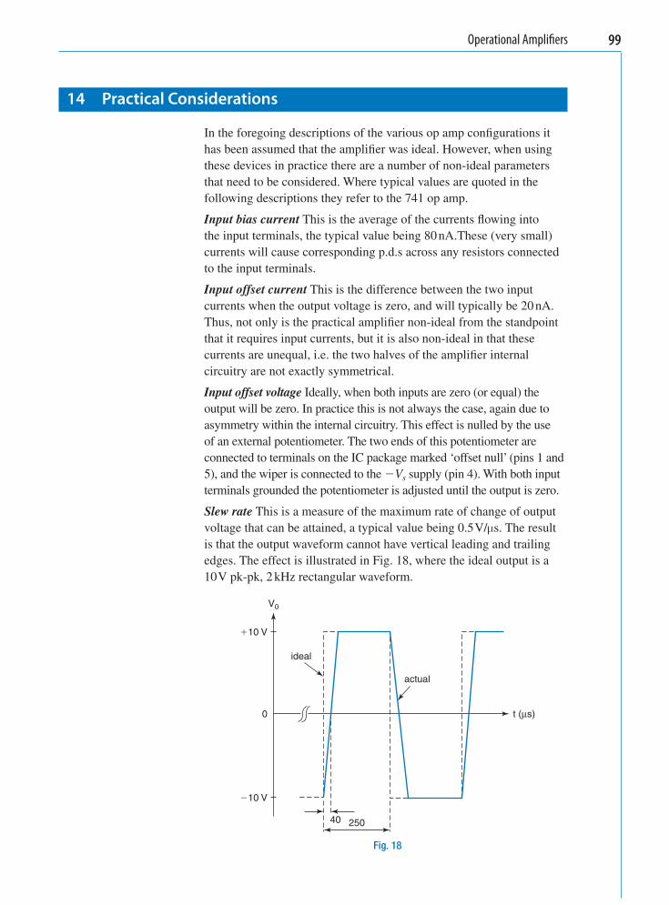
Slew rate This is a measure of the maximum rate of change of output voltage that can be attained, a typical value being 0.5 V/ µ s. The result is that the output waveform cannot have vertical leading and trailing edges. The effect is illustrated in Fig. 18 , where the ideal output is a 10 V pk-pk, 2 kHz rectangular waveform.
actual
ideal
10 V
10 V
0
V0
t (µs)
40 250
Fig. 18
WEBA-CH005.indd 99 5/2/2008 3:16:06 PM
100
From this fi gure it may be appreciated that the higher the frequency of the signal the more signifi cant will be the distortion of the output waveform.
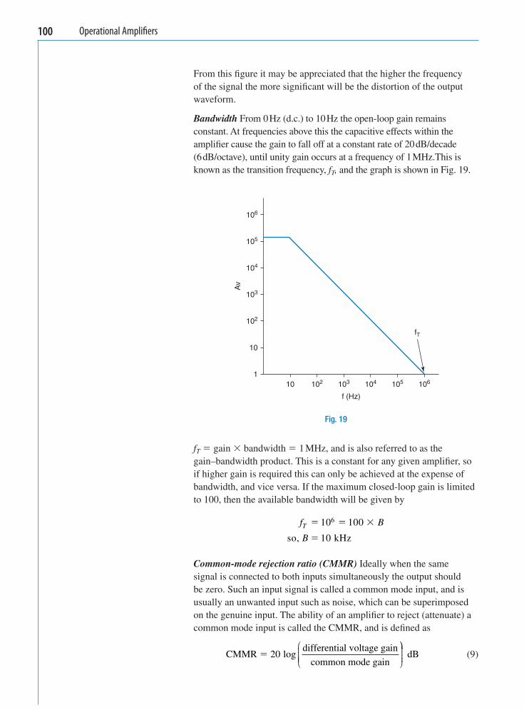
Bandwidth From 0 Hz (d.c.) to 10 Hz the open-loop gain remains constant. At frequencies above this the capacitive effects within the amplifi er cause the gain to fall off at a constant rate of 20dB/decade (6 dB/octave), until unity gain occurs at a frequency of 1 MHz.This is known as the transition frequency, f T , and the graph is shown in Fig. 19 .
106
105
104
103
102
102 103 104 105 106
10
110
f (Hz)
fT
Av
Fig. 19
f T gain bandwidth 1 MHz, and is also referred to as the gain–bandwidth product. This is a constant for any given amplifi er, so if higher gain is required this can only be achieved at the expense of bandwidth, and vice versa. If the maximum closed-loop gain is limited to 100, then the available bandwidth will be given by
f B
BT
10 100
10
6
so, kHz
Common-mode rejection ratio (CMMR) Ideally when the same signal is connected to both inputs simultaneously the output should be zero. Such an input signal is called a common mode input, and is usually an unwanted input such as noise, which can be superimposed on the genuine input. The ability of an amplifi er to reject (attenuate) a common mode input is called the CMMR, and is defi ned as
CMMR log
differential voltage gain
common mode gain 20
⎛
⎝⎜⎜⎜⎜
⎞⎞
⎠⎟⎟⎟⎟
dB (9)
Operational Amplifi ers
WEBA-CH005.indd 100 5/2/2008 3:16:06 PM
Operational Amplifi ers 101
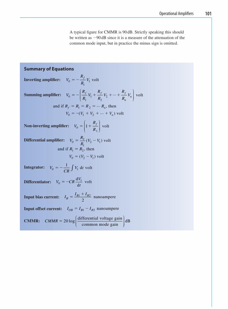
A typical fi gure for CMMR is 90 dB. Strictly speaking this should be written as 90 dB since it is a measure of the attenuation of the common mode input, but in practice the minus sign is omitted.
Summary of Equations
Inverting amplifi er: VR
RV0
f
11 volt
Summing amplifi er: VR
RV
R
RV
R
RV0
f f f
nn
11
22
... volt⎛
⎝⎜⎜⎜⎜
⎞
⎠⎟⎟⎟⎟⎟
and if ... , thenR R R Rf n 1 2
V V V V0 n ( ... ) volt1 2
Non-inverting amplifi er: VR
R0f
11
⎛
⎝⎜⎜⎜⎜
⎞
⎠⎟⎟⎟⎟⎟
volt
Differential amplifi er: VR
RV V0 2
12 1( ) volt
and if , then
( ) volt
R R
V V V0
1 2
2 1
Integrator: VCR
V t0 1
1 d volt∫
Differentiator: V CRV
t0 d
d volt1
Input bias current: II I
BB B
1 2
2 nanoampere
Input offset current: I I IOB B B 1 2 nanoampere
CMMR: CMMR 20 logdifferential voltage gain
common mode gain
⎛
⎝⎜⎜⎜⎜
⎞
⎠⎠⎟⎟⎟⎟
dB
WEBA-CH005.indd 101 5/2/2008 3:16:07 PM
Assignment Questions
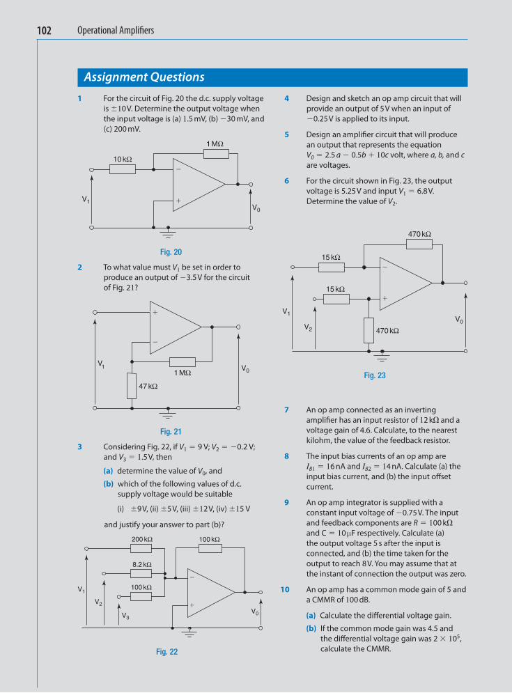
Operational Amplifi ers102
1 For the circuit of Fig. 20 the d.c. supply voltage is 10 V. Determine the output voltage when the input voltage is (a) 1.5 mV, (b) 30 mV, and (c) 200 mV.
4 Design and sketch an op amp circuit that will provide an output of 5 V when an input of 0.25 V is applied to its input.
5 Design an amplifi er circuit that will produce an output that represents the equation V 0 2.5 a 0.5 b 10 c volt, where a, b, and c are voltages.
6 For the circuit shown in Fig. 23 , the output voltage is 5.25 V and input V 1 6.8 V. Determine the value of V 2 .
V0
V1
10 kΩ
1 MΩ
Fig. 20
2 To what value must V 1 be set in order to produce an output of 3.5 V for the circuit of Fig. 21 ?
V1 V0
47 kΩ
1 MΩ
Fig. 21
3 Considering Fig. 22 , if V 1 9 V; V 2 0.2 V; and V 3 1.5 V, then
(a) determine the value of V 0 , and
(b) which of the following values of d.c. supply voltage would be suitable
(i) 9 V, (ii) 5 V, (iii) 12 V, (iv) 15 V
and justify your answer to part (b)?
V1
V2
V3V0
100 kΩ
8.2 kΩ
200 kΩ
100 kΩ
Fig. 22
V1
V2
V0
470 kΩ
470 kΩ
15 kΩ
15 kΩ
Fig. 23
7 An op amp connected as an inverting amplifi er has an input resistor of 12 k and a voltage gain of 4.6. Calculate, to the nearest kilohm, the value of the feedback resistor.
8 The input bias currents of an op amp are I B 1 16 nA and I B 2 14 nA. Calculate (a) the input bias current, and (b) the input off set current.
9 An op amp integrator is supplied with a constant input voltage of 0.75 V. The input and feedback components are R 100 k and C 10 µ F respectively. Calculate (a) the output voltage 5 s after the input is connected, and (b) the time taken for the output to reach 8 V. You may assume that at the instant of connection the output was zero.
10 An op amp has a common mode gain of 5 and a CMMR of 100 dB.
(a) Calculate the diff erential voltage gain.
(b) If the common mode gain was 4.5 and the diff erential voltage gain was 2 10 5 , calculate the CMMR.
WEBA-CH005.indd 102 5/2/2008 3:16:08 PM
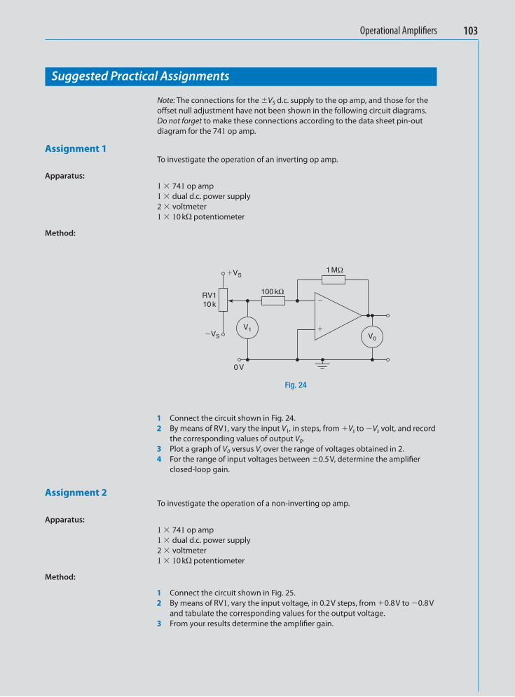
Suggested Practical Assignments
Note: The connections for the V S d.c. supply to the op amp, and those for the off set null adjustment have not been shown in the following circuit diagrams. Do not forget to make these connections according to the data sheet pin-out diagram for the 741 op amp.
Assignment 1 To investigate the operation of an inverting op amp .
Apparatus: 1 741 op amp 1 dual d.c. power supply 2 voltmeter 1 10 k potentiometer
Method:
Operational Amplifi ers 103
RV1 10 k
VS
0 V
VS
V1V0
100 kΩ
1 MΩ
Fig. 24
1 Connect the circuit shown in Fig. 24 . 2 By means of RV1, vary the input V 1 , in steps, from V s to V s volt, and record
the corresponding values of output V 0 . 3 Plot a graph of V 0 versus V i over the range of voltages obtained in 2. 4 For the range of input voltages between 0.5 V, determine the amplifi er
closed-loop gain.
Assignment 2 To investigate the operation of a non-inverting op amp.
Apparatus: 1 741 op amp 1 dual d.c. power supply 2 voltmeter 1 10 k potentiometer
Method:
1 Connect the circuit shown in Fig. 25 . 2 By means of RV1, vary the input voltage, in 0.2 V steps, from 0.8 V to 0.8 V
and tabulate the corresponding values for the output voltage. 3 From your results determine the amplifi er gain.
WEBA-CH005.indd 103 5/2/2008 3:16:10 PM
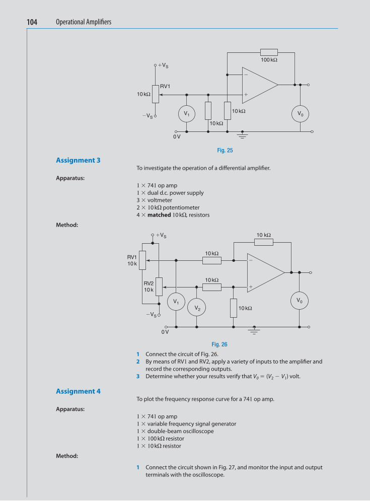
Assignment 3 To investigate the operation of a diff erential amplifi er.
Apparatus: 1 741 op amp 1 dual d.c. power supply 3 voltmeter 2 10 k potentiometer 4 matched 10 k , resistors
Method:
RV1
10 kΩ
10 kΩ
10 kΩ
100 kΩ
VS
VS
V1 V0
0 V
Fig. 25
RV1 10 k
RV2 10 k
10 kΩ
10 kΩ
10 kΩ
10 kΩVS
VS
0 V
V1V2
V0
Fig. 26
1 Connect the circuit of Fig. 26 . 2 By means of RV1 and RV2, apply a variety of inputs to the amplifi er and
record the corresponding outputs. 3 Determine whether your results verify that V 0 (V 2 V 1 ) volt.
Assignment 4 To plot the frequency response curve for a 741 op amp.
Apparatus: 1 741 op amp 1 variable frequency signal generator 1 double-beam oscilloscope 1 100 k resistor 1 10 k resistor
Method:
1 Connect the circuit shown in Fig. 27 , and monitor the input and output terminals with the oscilloscope.
Operational Amplifi ers104
WEBA-CH005.indd 104 5/2/2008 3:16:11 PM
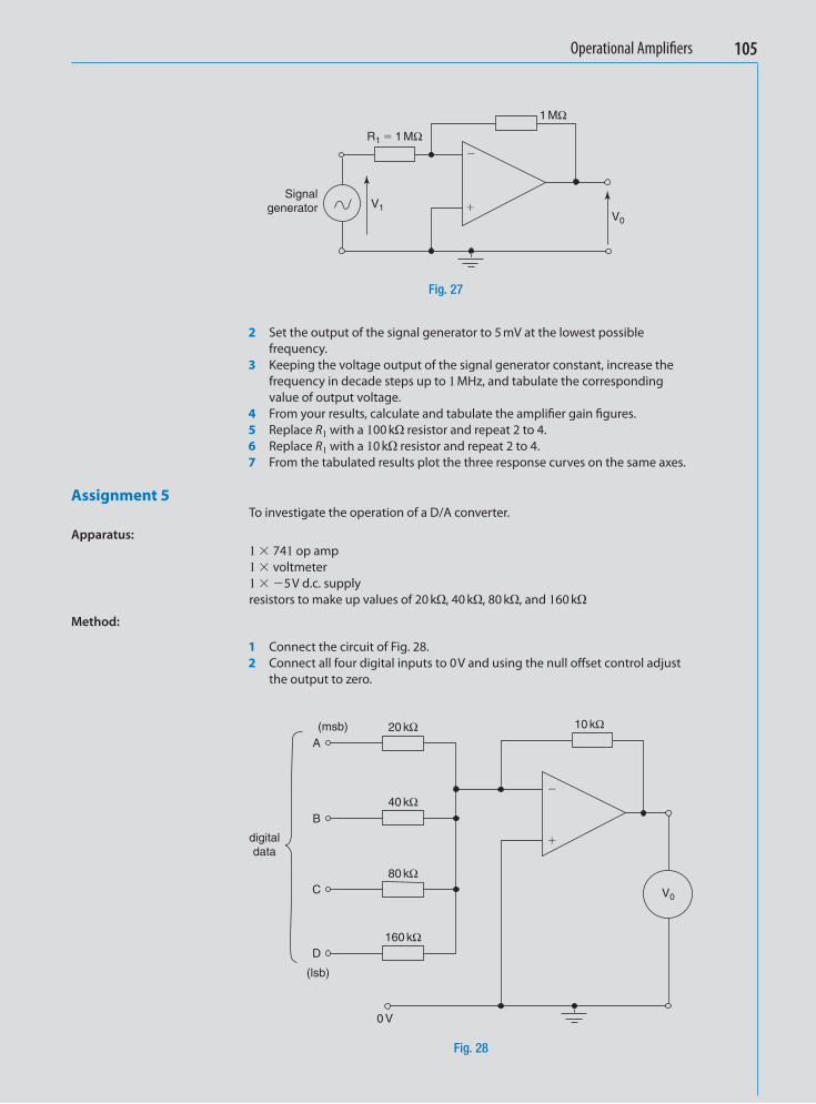
V0
V1
1 MΩ
R1 1 MΩ
Signal generator
Fig. 27
2 Set the output of the signal generator to 5 mV at the lowest possible frequency.
3 Keeping the voltage output of the signal generator constant, increase the frequency in decade steps up to 1 MHz, and tabulate the corresponding value of output voltage.
4 From your results, calculate and tabulate the amplifi er gain fi gures. 5 Replace R 1 with a 100 k resistor and repeat 2 to 4. 6 Replace R 1 with a 10 k resistor and repeat 2 to 4. 7 From the tabulated results plot the three response curves on the same axes.
Assignment 5 To investigate the operation of a D/A converter.
Apparatus: 1 741 op amp 1 voltmeter 1 5 V d.c. supply resistors to make up values of 20 k , 40 k , 80 k , and 160 k
Method:
1 Connect the circuit of Fig. 28 . 2 Connect all four digital inputs to 0 V and using the null off set control adjust
the output to zero.
Fig. 28
digital data
A
B
C
D
(msb)
(lsb)
20 kΩ 10 kΩ
40 kΩ
80 kΩ
160 kΩ
0 V
V0
Operational Amplifi ers 105
WEBA-CH005.indd 105 5/2/2008 3:16:12 PM
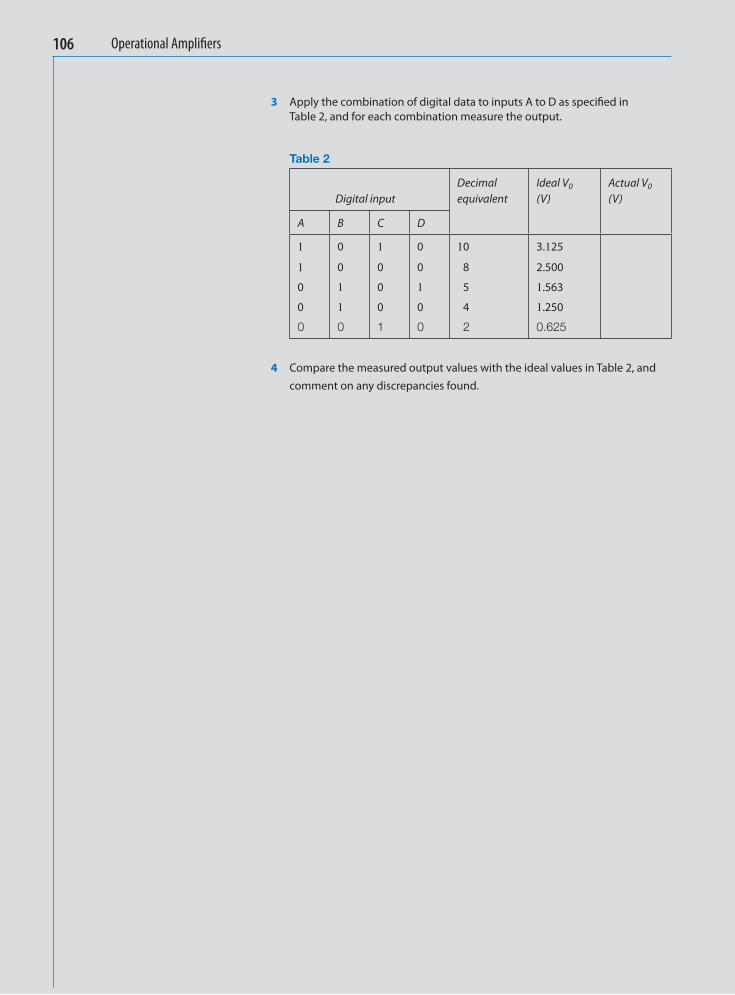
3 Apply the combination of digital data to inputs A to D as specifi ed in Table 2 , and for each combination measure the output.
106 Operational Amplifi ers
Table 2
Digital inputDecimal equivalent
Ideal V0 (V)
Actual V0 (V)
A B C D
1 0 1 0 10 3.125
1 0 0 0 8 2.500
0 1 0 1 5 1.563
0 1 0 0 4 1.250
0 0 1 0 2 0.625
4 Compare the measured output values with the ideal values in Table 2 , and comment on any discrepancies found.
WEBA-CH005.indd 106 5/2/2008 3:16:13 PM
Answers to Assignment Questions
1 (a) 150 mV (b) 3 V (c) 10 V (saturation)
2 157 mV
3 (a) 8.516 V (b) (i), (iii) and (iv)
4 Inverter with gain 20; say R f 1 M and R 1 50 k
5 Summer; if Rf 1 M then use 400 k , 2 M , 100 k for input resistors
6 6.97 V
7 55 k
8 (a) 15 nA (b) 2 nA
9 (a) 3.75 V b) 10.67 s
10 (a) 5 10 5 (b) 93 dB
Operational Amplifi ers 107
WEBA-CH005.indd 107 5/2/2008 3:16:13 PM