Embed Size (px)
Citation preview
Optical Properties of RotationallyTwinned InP Nanowire HeterostructuresJiming Bao,† David C. Bell,†,‡ and Federico Capasso*,†
School of Engineering and Applied Sciences, Center for Nanoscale Systems, HarVardUniVersity, Cambridge, Massachusetts 02138
Jakob B. Wagner
nCHREM Polymer and Materials Chemistry, Lund UniVersity,PO Box 124, SE-22100 Lund, Sweden
Thomas Mårtensson, Johanna Trägårdh, and Lars Samuelson
Solid State Physics, Lund UniVersity, PO Box 118, SE-22100 Lund, Sweden
Received November 8, 2007; Revised Manuscript Received January 18, 2008
ABSTRACT
We have developed a technique so that both transmission electron microscopy and microphotoluminescence can be performed on the samesemiconductor nanowire over a large range of optical power, thus allowing us to directly correlate structural and optical properties of rotationallytwinned zinc blende InP nanowires. We have constructed the energy band diagram of the resulting multiquantum well heterostructure andhave performed detailed quantum mechanical calculations of the electron and hole wave functions. The excitation power dependent blue-shiftof the photoluminescence can be explained in terms of the predicted staggered band alignment of the rotationally twinned zinc blende/wurziteInP heterostructure and of the concomitant diagonal transitions between localized electron and hole states responsible for radiative recombination.The ability of rotational twinning to introduce a heterostructure in a chemically homogeneous nanowire material and alter in a major way itsoptical properties opens new possibilities for band-structure engineering.
Nanotechnology based on semiconductor nanowires hasopened up new directions in band gap engineering ofoptoelectronic devices due to the large design space madepossible by the relaxation of many constraints typical of thinfilm growth.1–3 However the study of the structural andoptical properties of the same nanowire, which is essentialto correlate them in an unambiguous way, has not yet beenperformed. In order to establish this correlation, we havedeveloped a special grid so that both high-resolutiontransmission electron microscopy (HRTEM) and micro-photoluminescence (PL) measurements over a large rangeof optical power can be performed on the same nanowire.In contrast to bulk materials, nanowires are electron-transparent without further processing. This is important sincesample preparation methods such as mechanical polishingand ion milling may destroy or alter the optical properties.Using the new technique here reported, we have establisheda direct correlation between the structural and opticalproperties of rotationally twinned (RT) zinc blende (ZB) InP
nanowires.4–6 RT heterostructures observed in these nano-wires are based on a heterojunction consisting of adjacentrotated lattices in InP. The observed power dependent blueshift of the PL spectra can be qualitatively explained bymodeling the electron and hole wave functions of the InPnanowire heterostructure based on TEM lattice image andthe predicted staggered heterojunction band alignment be-tween ZB InP and twinning associated wurtzite (WZ) InP.7
RT, if suitably controlled, could add a new dimension innanostructure device design.8,9
Both WZ (hexagonal) and ZB (cubic) lattices belong tothe close-packed crystal structure, and many materials cancrystallize in either form or in a mixed structure (so-calledpolytype) under specific conditions.10–12 A stacking fault isa type of plane defect in ZB or WZ crystals.10,13,14 In RTZB crystals, lattices adjacent to the twin plane have the sameZB structure, but they are rotated 180° around the ⟨111⟩growth direction.10,13–15 As shown in Figure 1a, a RT structurecan be regarded as one layer of stacking fault.10,13–15 Stackingfaults have been found to contribute to many phenomena,for example, an unexpectedly large photovoltaic effect.16,17
In the models developed, many of these observations were
* To whom correspondence may be addressed.† School of Engineering and Applied Sciences.‡ Center for Nanoscale Systems.
NANOLETTERS
2008Vol. 8, No. 3
836-841
10.1021/nl072921e CCC: $40.75 2008 American Chemical SocietyPublished on Web 02/15/2008
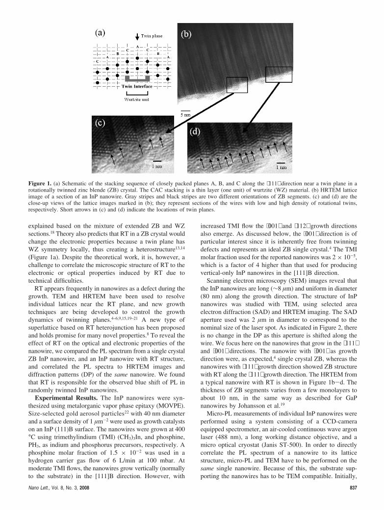
explained based on the mixture of extended ZB and WZsections.18 Theory also predicts that RT in a ZB crystal wouldchange the electronic properties because a twin plane hasWZ symmetry locally, thus creating a heterostructure13,14
(Figure 1a). Despite the theoretical work, it is, however, achallenge to correlate the microscopic structure of RT to theelectronic or optical properties induced by RT due totechnical difficulties.
RT appears frequently in nanowires as a defect during thegrowth. TEM and HRTEM have been used to resolveindividual lattices near the RT plane, and new growthtechniques are being developed to control the growthdynamics of twinning planes.4–6,9,15,19–21 A new type ofsuperlattice based on RT heterojunction has been proposedand holds promise for many novel properties.8 To reveal theeffect of RT on the optical and electronic properties of thenanowire, we compared the PL spectrum from a single crystalZB InP nanowire, and an InP nanowire with RT structure,and correlated the PL spectra to HRTEM images anddiffraction patterns (DP) of the same nanowire. We foundthat RT is responsible for the observed blue shift of PL inrandomly twinned InP nanowires.
Experimental Results. The InP nanowires were syn-thesized using metalorganic vapor phase epitaxy (MOVPE).Size-selected gold aerosol particles22 with 40 nm diameterand a surface density of 1 µm-2 were used as growth catalystson an InP (111)B surface. The nanowires were grown at 400°C using trimethylindium (TMI) (CH3)3In, and phosphine,PH3, as indium and phosphorus precursors, respectively. Aphosphine molar fraction of 1.5 × 10⁻² was used in ahydrogen carrier gas flow of 6 L/min at 100 mbar. Atmoderate TMI flows, the nanowires grow vertically (normallyto the substrate) in the [111]B direction. However, with
increased TMI flow the ⟨001⟩ and ⟨112⟩ growth directionsalso emerge. As discussed below, the ⟨001⟩ direction is ofparticular interest since it is inherently free from twinningdefects and represents an ideal ZB single crystal.4 The TMImolar fraction used for the reported nanowires was 2 × 10⁻⁵,which is a factor of 4 higher than that used for producingvertical-only InP nanowires in the [111]B direction.
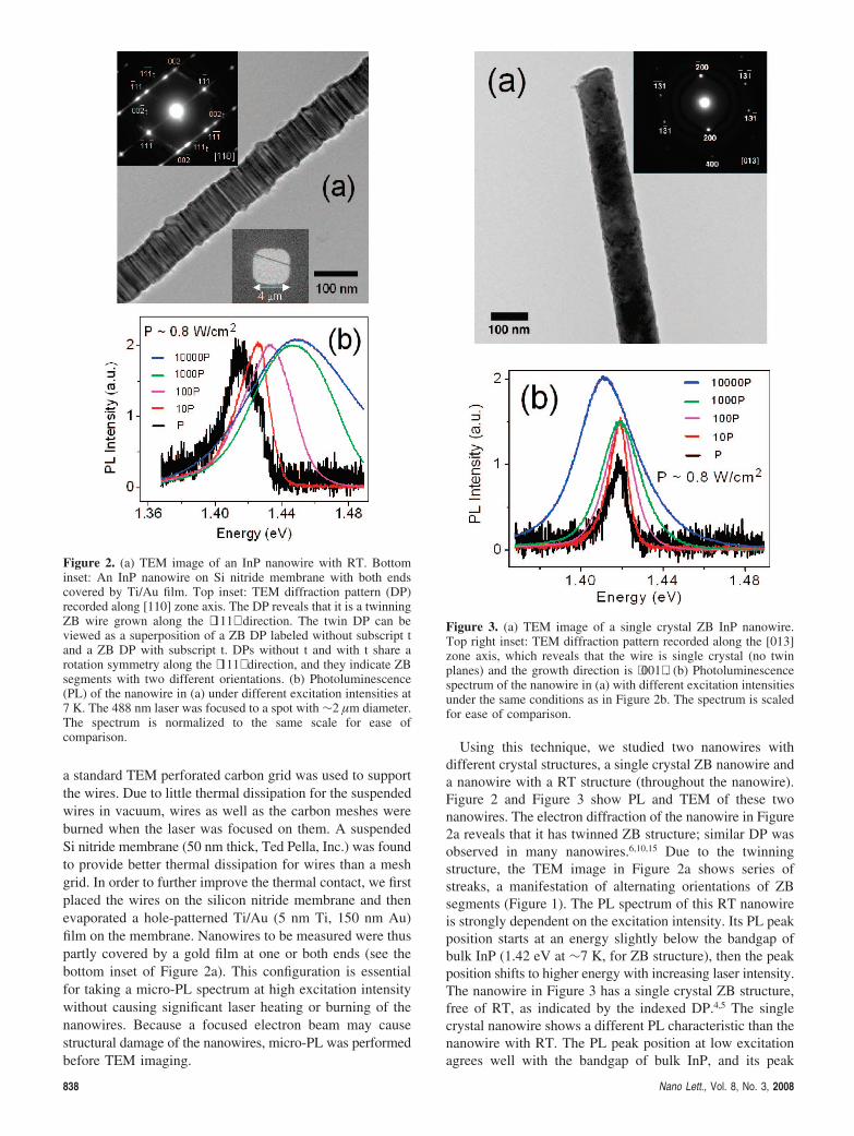
Scanning electron microscopy (SEM) images reveal thatthe InP nanowires are long (∼8 µm) and uniform in diameter(80 nm) along the growth direction. The structure of InPnanowires was studied with TEM, using selected areaelectron diffraction (SAD) and HRTEM imaging. The SADaperture used was 2 µm in diameter to correspond to thenominal size of the laser spot. As indicated in Figure 2, thereis no change in the DP as this aperture is shifted along thewire. We focus here on the nanowires that grow in the ⟨111⟩and ⟨001⟩ directions. The nanowire with ⟨001⟩ as growthdirection were, as expected,4 single crystal ZB, whereas thenanowires with ⟨111⟩ growth direction showed ZB structurewith RT along the ⟨111⟩ growth direction. The HRTEM froma typical nanowire with RT is shown in Figure 1b-d. Thethickness of ZB segments varies from a few monolayers toabout 10 nm, in the same way as described for GaPnanowires by Johansson et al.19
Micro-PL measurements of individual InP nanowires wereperformed using a system consisting of a CCD-cameraequipped spectrometer, an air-cooled continuous wave argonlaser (488 nm), a long working distance objective, and amicro optical cryostat (Janis ST-500). In order to directlycorrelate the PL spectrum of a nanowire to its latticestructure, micro-PL and TEM have to be performed on thesame single nanowire. Because of this, the substrate sup-porting the nanowires has to be TEM compatible. Initially,
Figure 1. (a) Schematic of the stacking sequence of closely packed planes A, B, and C along the ⟨111⟩ direction near a twin plane in arotationally twinned zinc blende (ZB) crystal. The CAC stacking is a thin layer (one unit) of wurtzite (WZ) material. (b) HRTEM latticeimage of a section of an InP nanowire. Gray stripes and black stripes are two different orientations of ZB segments. (c) and (d) are theclose-up views of the lattice images marked in (b); they represent sections of the wires with low and high density of rotational twins,respectively. Short arrows in (c) and (d) indicate the locations of twin planes.
Nano Lett., Vol. 8, No. 3, 2008 837
a standard TEM perforated carbon grid was used to supportthe wires. Due to little thermal dissipation for the suspendedwires in vacuum, wires as well as the carbon meshes wereburned when the laser was focused on them. A suspendedSi nitride membrane (50 nm thick, Ted Pella, Inc.) was foundto provide better thermal dissipation for wires than a meshgrid. In order to further improve the thermal contact, we firstplaced the wires on the silicon nitride membrane and thenevaporated a hole-patterned Ti/Au (5 nm Ti, 150 nm Au)film on the membrane. Nanowires to be measured were thuspartly covered by a gold film at one or both ends (see thebottom inset of Figure 2a). This configuration is essentialfor taking a micro-PL spectrum at high excitation intensitywithout causing significant laser heating or burning of thenanowires. Because a focused electron beam may causestructural damage of the nanowires, micro-PL was performedbefore TEM imaging.
Using this technique, we studied two nanowires withdifferent crystal structures, a single crystal ZB nanowire anda nanowire with a RT structure (throughout the nanowire).Figure 2 and Figure 3 show PL and TEM of these twonanowires. The electron diffraction of the nanowire in Figure2a reveals that it has twinned ZB structure; similar DP wasobserved in many nanowires.6,10,15 Due to the twinningstructure, the TEM image in Figure 2a shows series ofstreaks, a manifestation of alternating orientations of ZBsegments (Figure 1). The PL spectrum of this RT nanowireis strongly dependent on the excitation intensity. Its PL peakposition starts at an energy slightly below the bandgap ofbulk InP (1.42 eV at ∼7 K, for ZB structure), then the peakposition shifts to higher energy with increasing laser intensity.The nanowire in Figure 3 has a single crystal ZB structure,free of RT, as indicated by the indexed DP.4,5 The singlecrystal nanowire shows a different PL characteristic than thenanowire with RT. The PL peak position at low excitationagrees well with the bandgap of bulk InP, and its peak
Figure 2. (a) TEM image of an InP nanowire with RT. Bottominset: An InP nanowire on Si nitride membrane with both endscovered by Ti/Au film. Top inset: TEM diffraction pattern (DP)recorded along [110] zone axis. The DP reveals that it is a twinningZB wire grown along the ⟨111⟩ direction. The twin DP can beviewed as a superposition of a ZB DP labeled without subscript tand a ZB DP with subscript t. DPs without t and with t share arotation symmetry along the ⟨111⟩ direction, and they indicate ZBsegments with two different orientations. (b) Photoluminescence(PL) of the nanowire in (a) under different excitation intensities at7 K. The 488 nm laser was focused to a spot with ∼2 µm diameter.The spectrum is normalized to the same scale for ease ofcomparison.
Figure 3. (a) TEM image of a single crystal ZB InP nanowire.Top right inset: TEM diffraction pattern recorded along the [013]zone axis, which reveals that the wire is single crystal (no twinplanes) and the growth direction is ⟨001⟩ . (b) Photoluminescencespectrum of the nanowire in (a) with different excitation intensitiesunder the same conditions as in Figure 2b. The spectrum is scaledfor ease of comparison.
838 Nano Lett., Vol. 8, No. 3, 2008
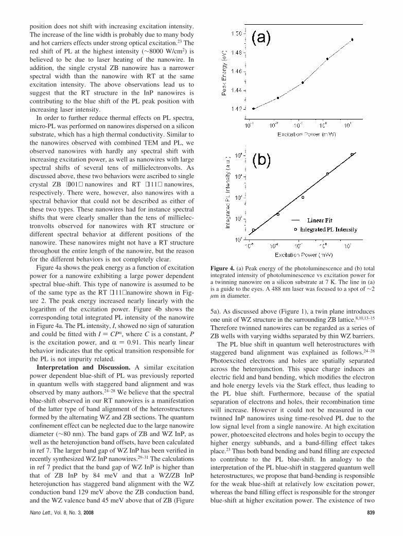
position does not shift with increasing excitation intensity.The increase of the line width is probably due to many bodyand hot carriers effects under strong optical excitation.23 Thered shift of PL at the highest intensity (∼8000 W/cm2) isbelieved to be due to laser heating of the nanowire. Inaddition, the single crystal ZB nanowire has a narrowerspectral width than the nanowire with RT at the sameexcitation intensity. The above observations lead us tosuggest that the RT structure in the InP nanowires iscontributing to the blue shift of the PL peak position withincreasing laser intensity.
In order to further reduce thermal effects on PL spectra,micro-PL was performed on nanowires dispersed on a siliconsubstrate, which has a high thermal conductivity. Similar tothe nanowires observed with combined TEM and PL, weobserved nanowires with hardly any spectral shift withincreasing excitation power, as well as nanowires with largespectral shifts of several tens of millielectronvolts. Asdiscussed above, these two behaviors were ascribed to singlecrystal ZB ⟨001⟩ nanowires and RT ⟨111⟩ nanowires,respectively. There were, however, also nanowires with aspectral behavior that could not be described as either ofthese two types. These nanowires had for instance spectralshifts that were clearly smaller than the tens of millielec-tronvolts observed for nanowires with RT structure ordifferent spectral behavior at different positions of thenanowire. These nanowires might not have a RT structurethroughout the entire length of the nanowire, but the reasonfor the different behaviors is not completely clear.
Figure 4a shows the peak energy as a function of excitationpower for a nanowire exhibiting a large power dependentspectral blue-shift. This type of nanowire is assumed to beof the same type as the RT ⟨111⟩ nanowire shown in Fig-ure 2. The peak energy increased nearly linearly with thelogarithm of the excitation power. Figure 4b shows thecorresponding total integrated PL intensity of the nanowirein Figure 4a. The PL intensity, I, showed no sign of saturationand could be fitted with I ) CPR, where C is a constant, Pis the excitation power, and R ) 0.91. This nearly linearbehavior indicates that the optical transition responsible forthe PL is not impurity related.
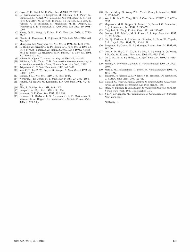
Interpretation and Discussion. A similar excitationpower dependent blue-shift of PL was previously reportedin quantum wells with staggered band alignment and wasobserved by many authors.24–28 We believe that the spectralblue-shift observed in our RT nanowires is a manifestationof the latter type of band alignment of the heterostructuresformed by the alternating WZ and ZB sections. The quantumconfinement effect can be neglected due to the large nanowirediameter (∼80 nm). The band gaps of ZB and WZ InP, aswell as the heterojunction band offsets, have been calculatedin ref 7. The larger band gap of WZ InP has been verified inrecently synthesized WZ InP nanowires.29–31 The calculationsin ref 7 predict that the band gap of WZ InP is higher thanthat of ZB InP by 84 meV and that a WZ/ZB InPheterojunction has staggered band alignment with the WZconduction band 129 meV above the ZB conduction band,and the WZ valence band 45 meV above that of ZB (Figure
5a). As discussed above (Figure 1), a twin plane introducesone unit of WZ structure in the surrounding ZB lattice.8,10,13–15
Therefore twinned nanowires can be regarded as a series ofZB wells with varying widths separated by thin WZ barriers.
The PL blue shift in quantum well heterostructures withstaggered band alignment was explained as follows.24–28
Photoexcited electrons and holes are spatially separatedacross the heterojunction. This space charge induces anelectric field and band bending, which modifies the electronand hole energy levels via the Stark effect, thus leading tothe PL blue shift. Furthermore, because of the spatialseparation of electrons and holes, their recombination timewill increase. However it could not be measured in ourtwinned InP nanowires using time-resolved PL due to thelow signal level from a single nanowire. At high excitationpower, photoexcited electrons and holes begin to occupy thehigher energy subbands, and a band-filling effect takesplace.23 Thus both band bending and band filling are expectedto contribute to the PL blue-shift. In analogy to theinterpretation of the PL blue-shift in staggered quantum wellheterostructures, we propose that band-bending is responsiblefor the weak blue-shift at relatively low excitation power,whereas the band filling effect is responsible for the strongerblue-shift at higher excitation power. The existence of two
Figure 4. (a) Peak energy of the photoluminescence and (b) totalintegrated intensity of photoluminescence vs excitation power fora twinning nanowire on a silicon substrate at 7 K. The line in (a)is a guide to the eyes. A 488 nm laser was focused to a spot of ∼2µm in diameter.
Nano Lett., Vol. 8, No. 3, 2008 839
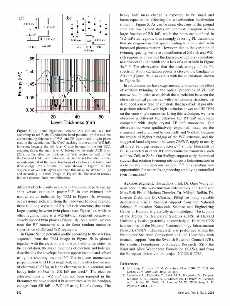
different effects results in a kink in the curve of peak energyshift versus excitation power.24–27 In our twinned InPnanowires, as indicated by TEM in Figure 1b, twinningoccurs nonperiodically along the nanowire. In some regions,there is a long segment of ZB-InP-rich structure, due to thelarge spacing between twin planes (see Figure 1c), while inother regions, there is a WZ-InP-rich segment because ofclosely spaced twin planes (Figure 1d). As a result, we cantreat the RT nanowire as a de facto random nanowiresuperlattice of ZB and WZ segments.
In Figure 5c the potential profile according to the stackingsequence from the TEM image in Figure 2b is plottedtogether with the electron and hole probability densities. Inthe calculation, the wave functions of electron and hole aredescribed by the envelope function approximation and solvedusing the shooting method.32,33 The in-plane momentumperpendicular to ⟨111⟩ is neglected, and the effective massesof electrons (0.073m, m is the electron mass in vacuum) andheavy holes (0.58m) in ZB InP are used.34 The electroneffective mass in WZ InP has not been reported in theliterature; we have scaled it in accordance with the bandgapchange from ZB InP to WZ InP using Kane’s theory. The
heavy hole mass change is expected to be small andinconsequential in affecting the wavefunction localizationshown in Figure 5. As can be seen, electrons in the groundstate and low excited states are confined in regions with alarge fraction of ZB InP, while the holes are confined inWZ-InP-rich regions, thus strongly favoring PL transitionsthat are diagonal in real space, leading to a blue shift withincreased photoexcitation. However, due to the variation oftwinning spacing, we have a distribution of ZB-rich and WZ-rich regions with various thicknesses, which may contributeto a broader PL line width and a lack of a clear kink in Figure4a.24–27 The observation that the peak energy of the PLspectrum at low excitation power is close to the bandgap ofZB InP (Figure 2b) also agrees with the calculations shownin Figure 5c.
In conclusion, we have experimentally observed the effectof rotation twinning on the optical properties of ZB InPnanowires. In order to establish the correlation between theobserved optical properties with the twinning structure, wedeveloped a new type of substrate that has made it possibleto perform micro-PL with high excitation power and HRTEMon the same single nanowire. Using this technique, we haveobserved a different PL behavior for RT InP nanowirescompared with single crystal ZB InP nanowires. Ourobservations were qualitatively explained based on thestaggered band alignment between ZB- and WZ-InP. Becausethe results of higher bandgap of the WZ structure, and thestaggered band alignment between ZB/WZ, apply to nearlyall direct bandgap semiconductors,7,28 similar blue-shift ofPL is expected in other RT semiconductor nanowires suchas InAs, ZnS, or ZnSe. Our findings support early theoreticalstudies that rotation twinning introduces a heterojunction ina chemically homogeneous material,13,14 thus creating newopportunities for materials engineering employing controlledtwin formation.8
Acknowledgment. The authors thank Dr. Qijie Wang forassistance in the wavefunction calculations and ProfessorMats-Erik Pistol, Mariano Zimmler, Dr. Mikhail Belkin, Dr.Laurent Diehl, and Dr. Christian Pflügl for many valuablediscussions. Partial financial support from the NationalScience Foundation Nanoscale Science and EngineeringCenter at Harvard is gratefully acknowledged. The supportof the Center for Nanoscale Systems (CNS) at HarvardUniversity is also gratefully acknowledged. Harvard CNSis a member of the National Nanotechnology InfrastructureNetwork (NNIN). This research was performed within theNanometer Structure Consortium at Lund University withfinancial support from the Swedish Research Council (VR),the Swedish Foundation for Strategic Research (SSF), theKnut and Alice Wallenberg Foundation (KAW), and fromthe European Union via the project NODE 015783.
References(1) (a) Huang, Y.; Lieber, C. M. Pure Appl. Chem. 2004, 76, 2051. (b)
Lieber, C. M. MRS Bull. 2003, 28, 486.(2) Samuelson, L.; Thelander, C.; Björk, M. T.; Borgström, M.; Deppert,
K.; Dick, K. A.; Hansen, A. E.; Mårtensson, T.; Panev, N.; Persson,A. I.; Seifert, W.; Sköld, N.; Larsson, M. W.; Wallenberg, L. R.Physica E 2004, 25, 313.
Figure 5. (a) Band alignment between ZB InP and WZ InPaccording to ref 7. (b) Conduction band potential profile and thecorresponding thickness of WZ and ZB layers near a twin planeused in the calculation. The CAC stacking is one unit of WZ InP;however, because the left layer C also belongs to the left BCAstacking (ZB), the right layer C belongs to the right ACB layer(ZB), so the effective thickness of WZ section is half of thethickness of CAC layer, which is ∼0.34 nm. (c) Potential profile,moduli squared of the wave functions of electrons and holes, andtheir energy levels for the RT wire shown in Figure 1b. Thesequence of WZ/ZB layers and their thickness are defined in (b)and according to lattice image in Figure 1b. The dashed arrowsindicate electron–hole recombination.
840 Nano Lett., Vol. 8, No. 3, 2008
(3) Pryor, C. E.; Pistol, M. E. Phys. ReV. B 2005, 72, 205311.(4) (a) Krishnamachari, U.; Borgstrom, M.; Ohlsson, B. J.; Panev, N.;
Samuelson, L.; Seifert, W.; Larsson, M. W.; Wallenberg, L. R. Appl.Phys. Lett. 2004, 85, 2077. (b) Björk, M. T.; Ohlsson, B. J.; Sass, T.;Persson, A. I.; Thelander, C.; Magnusson, M. H.; Deppert, K.;Wallenberg, L. R.; Samuelson, L. Appl. Phys. Lett. 2002, 80, 1058–1060.
(5) Xiong, Q. H.; Wang, J.; Eklund, P. C. Nano Lett. 2006, 6, 2736–2742.
(6) Bhunia, S.; Kawamura, T.; Fujikawa, S. Thin Solid Films 2004, 464,244–247.
(7) Murayama, M.; Nakayama, T. Phys. ReV. B 1994, 49, 4710–4724.(8) (a) Ikonic, Z.; Srivastava, G. P.; Inkson, J. C. Phys. ReV. B 1995, 52,
1474–1476. (b) Bandic, Z. Z.; Ikonic, Z. Phys. ReV. B 1995, 51, 9806–9812. (c) Ikonic, Z.; Srivastava, G. P.; Inkson, J. C. Surf. Sci. 1994,307–309, 880–884.
(9) Hibino, H.; Ogino, T. Mater. Sci. Eng., B 2001, 87, 214–221.(10) Williams, D. B.; Carter, C. B. Transmission electron microscopy: a
textbook for materials science; Plenum Press: New York, 1996.(11) Trigunayat, G. C. Solid State Ionics 1991, 48, 3–70.(12) Yeh, C. Y.; Lu, Z. W.; Froyen, S.; Zunger, A. Phys. ReV. B 1992, 46,
10086–10097.(13) Birman, J. L. Phys. ReV. 1959, 115, 1493–1505.(14) Northrup, J. E.; Cohen, M. L. Phys. ReV. B 1981, 23, 2563–2566.(15) Hiruma, K.; Yazawa, M.; Katsuyama, T. J. Appl. Phys. 1995, 77, 447–
462.(16) Ellis, S. G. Phys. ReV. 1958, 109, 1860.(17) Lempicki, A. Phys. ReV. 1959, 113, 1204.(18) Neumark, G. F. Phys. ReV. 1962, 125, 838.(19) Johansson, J.; Karlsson, L. S.; Svensson, C. P. T.; Martensson, T.;
Wacaser, B. A.; Deppert, K.; Samuelson, L.; Seifert, W. Nat. Mater.2006, 5, 574–580.
(20) Hao, Y.; Meng, G.; Wang, Z. L.; Ye, C.; Zhang, L. Nano Lett. 2006,6, 1650–1655.
(21) Wu, R. B.; Pan, Y.; Yang, G. Y. J. Phys. Chem. C 2007, 111, 6233–6237.
(22) Magnusson, M. H.; Deppert, K.; Malm, J. O.; Bovin, J. O.; Samuelson,L. g. J. Nanopart. Res. 1999, 1, 243–251.
(23) Cingolani, R.; Ploog, K. AdV. Phys. 1991, 40, 535–623.(24) Fouquet, J. E.; Minsky, M. S.; Rosner, S. J. Appl. Phys. Lett. 1993,
63, 3212–3214.(25) Liu, Q.; Derksen, S.; Lindner, A.; Scheffer, F.; Prost, W.; Tegude,
F.-J. J. Appl. Phys. 1995, 77, 1154–1158.(26) Benyattou, T.; Garcia, M. A.; Moneger, S. Appl. Surf. Sci. 1993, 63,
197–201.(27) Luo, X. D.; Hu, C. Y.; Xu, Z. Y.; Luo, H. L.; Wang, Y. Q.; Wang,
J. N.; Ge, W. K. Appl. Phys. Lett. 2002, 81, 3795–3797.(28) Lu, X. H.; Yu, P. Y.; Zheng, L. X. Appl. Phys. Lett. 2003, 82, 1033–
1035.(29) Mohan, P.; Motohisa, J.; Fukui, T. Nanotechnology 2005, 16, 2903–
2907.(30) Mattila, M.; Hakkarainen, T.; Mulot, M. Nanotechnology 2006, 17,
1580–1583.(31) Tragardh, J.; Persson, A. I.; Wagner, J. B.; Hessman, D.; Samuelson,
L. J. Appl. Phys. 2007, 101, 123701.(32) Bastard, G. WaVe mechanics applied to semiconductor heterostruc-
tures; Les éditions de physique; Les Ulis: France, 1988.(33) Stoer, J.; Bulirsch, R. Introduction to Numerical Analysis; Springer-
Verlag: New York, 1980 . (see Section 7.3).(34) Yu, P. Y.; Cardona, M. Fundamentals of Semiconductors; Springer:
New York, 2001.
NL072921E
Nano Lett., Vol. 8, No. 3, 2008 841