Embed Size (px)
Citation preview
Optical simulation of terahertz antenna using
finite difference time domain method
by
Chao Zhang
A Thesis Submitted in Partial Fulfillment of the Requirements for the Degree of
Master of Science in the Chester F. Carlson Center for Imaging Science
College of Science
Rochester Institute of Technology
December, 2014
Signature of the Author______________________________________________________________
Accepted by__________________________________________________________________________
Director, M.S. Degree Program Date
ii
CHESTER F. CARLSON CENTER FOR IMAGING SCIENCE
COLLEGE OF SCIENCE
ROCHESTER INSITITUTE OF TECHNOLOGY
ROCHESTER, NEW YORK
CERTIFICATE OF APPROVAL
______________________________________________________________________________________
M.S. DEGREE THESIS
_____________________________________________________________________________________
The M.S. degree Thesis of Chao Zhang has been examined and approved by the
thesis committee as satisfactory for the thesis requirement for the Master of Science degree
______________________________________________
Dr. Zoran Ninkov, Thesis Advisor
______________________________________________
Dr. Robert Kremens, Committee Member
______________________________________________
Dr. Alan Raisanen, Committee Member
______________________________________________
Date
iii
Acknowledgements
At first, it is my great pleasure to work with my thesis advisor, Professor Zoran Ninkov,
for his valuable advice and guidance through my two-year experience at CIS. He is
always encouraging and often tells me to start work from the most fundamental physics
and then to more deep thinking. His enthusiasm and passion to the research have a great
influence on me. Not a single word could express my gratitude to him.
Thanks Dr Robert Kremens and Dr Alan Raisanen for kindly be the committee members
and taking time to review this thesis.
As members of the research project, Paul Lee, Andy Sacco, Dan Newman, Kenny
Fourspring and others always inspire me to make progress. Greg Fertig, Dmitry
Vorobiev, Ross Robinson often offer help in the lab. Wish all of them happy life and
successful career.
Thanks to the faculty, staff and students at CIS for I had a great time with all of them. As
an international student, they compose most of my life here.
Finally, my parents are the persons from whom I could obtain courage and comfort. Wish
them to be healthy and expect them to enjoy the life.
iv
Abstract
Terahertz science is a promising and rapidly developing research area. However, solid
state terahertz detectors of high performance are still needed. An antenna within each
pixel is needed in these detectors so as to couple more incident radiation into the detector.
In this thesis, a software package called Lumerical FDTD Solutions is used to optimize
the terahertz antenna design. The ultimate goal is to design broadband antennas that work
efficiently over desired frequency bands.
The transmission/absorption characteristics of various bowtie antennas were modeled
using the software. For absorption modeling, an equivalent resistor was added to load the
antenna and absorb the terahertz energy. The effect of various parameters, including
geometrical shape, boundary condition, material index, were considered. Fat bowtie was
chosen as the optimum design for a 215GHz antenna. Optimization was carried out to
check how the gap, slot, distance between metal contacts would affect the performance of
the antenna. A transmission experiment was designed to verify the validity of these
simulations using a 188GHz source. Finally, some tests for the angular response of
silicon/air interface and dipole antenna were done, in order to ascertain the efficiency of
coupling between the optical telescope used to collect the THz radiation and the
antenna/detector combination.

v
Table of Contents
Acknowledgements..................................................................................................................iii
Abstract.................................................................................................................................. iv
Table of Contents..................................................................................................................... v
List of Figures ........................................................................................................................vii
List of Tables........................................................................................................................ xvii
1. Introduction ......................................................................................................................... 1
1.1 Terahertz radiation .............................................................................................. 1
1.2. Properties of Terahertz Waves ............................................................................ 2
1.2.1. Non-ionizing radiation ................................................................................. 2
1.2.2. Terahertz penetration and transmission ......................................................... 3
1.2.3. Some other terahertz wave properties ........................................................... 5
1.3. Applications of Terahertz radiation ..................................................................... 5
1.3.1. Security ....................................................................................................... 5
1.3.2. Terahertz spectroscopy identification............................................................ 8
1.3.3. Terahertz Medical Imaging ........................................................................ 10
1.3.4. Some other applications ............................................................................. 12
1.4. Summary ......................................................................................................... 13
2. MOSFET detection ............................................................................................................ 14
2.1. Direct and heterodyne THz detection ................................................................ 14
2.2. Photon and thermal detectors ............................................................................ 17
2.3. MOSFET detection........................................................................................... 20
3. Numerical method, realization and simulation model .......................................................... 25
3.1. Finite Difference Time Domain method ............................................................ 25
3.2. Lumerical FDTD Solutions ............................................................................... 28
3.3. Simulation model ............................................................................................. 31
4. Effects of different parameters on the antenna performance ................................................. 39
4.1. Material index .................................................................................................. 39
4.2. Comparison of simulation results to existing references ..................................... 45
4.3. Effect of antenna pixel pitch ............................................................................. 50
vi
4.4. Broadband bowtie antenna ................................................................................ 52
4.5. Polarization ...................................................................................................... 58
4.6. Periodic boundary ............................................................................................ 59
4.7. Load resistance................................................................................................. 62
4.8. E-field distribution from antenna to detector ...................................................... 63
4.9. Antenna thickness ............................................................................................ 66
5. 215GHz & 188GHz Antenna Design .................................................................................. 68
5.1. 215 GHz bowtie antenna design ........................................................................ 68
5.1.1. Frequency design ....................................................................................... 68
5.1.2. Effect of slots in the antenna ...................................................................... 78
5.1.3. Effect of antenna gap ................................................................................. 86
5.2. 188 GHz transmission experiment design .......................................................... 94
5.3. Angular response of antenna ............................................................................. 98
5.4. Conclusion and future work ............................................................................ 104

vii
List of Figures
Figure 1.1. Terahertz region in the electromagnetic spectrum [2]
Figure 1.2. Non-ionizing property of Terahertz wave
Figure 1.3. Absorption spectra of different explosives (left) and other substances
(right) measured at THz frequencies [9]
Figure 1.4. Measured and simulated transmission spectra for a THz path length
of 0.45m at an ambient temperature of 20 degree centigrade and 30%
humidity [11]
Figure 1.5. ThruVision TS5 people screening system (upper) and Weapon
detection of a person with a hammer [13]
Figure 1.6. A tiny terahertz detection device detecting the hidden bullets
inside a toy bear [14]
Figure 1.7. Mini-Z THz Time Domain Spectrometer [15]
Figure 1.8. THz spectroscopy identification of substance sealed in a letter.
Screenshots from the introduction video of Mini-Z [15]
Figure 1.9. Imaging results of a tissue for THz (left) and Visible (right) [16]
viii
Figure 1.10. THz image of an artificially contaminated chocolate bar: a stone
(solid circle), a M2 metal screw (dashed circle) and a glass splinter (dotted
circle) [19]
Figure 2.1. Schematic representation of a direct detection. WS is the signal
power and WB is the background radiation power. [20]
Figure 2.2. Schematic representation of heterodyne detection
Figure 2.3. Schematic diagram of thermal detector
Figure 2.4. Schematic diagram of bolometer
Figure 2.5. n-MOSFET diagram [29]
Figure 2.6. Metal-oxide-semiconductor structure on p-type silicon
Figure 2.7. Plasma oscillations in MOSFET [20]
Figure 2.8. MOSFET THz detection with biased voltage, however, the biased
current between source and drain is not included
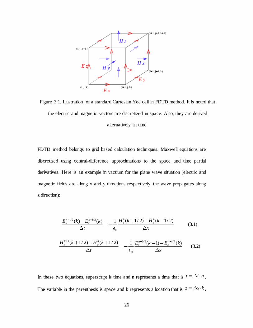
Figure 3.1. Illustration of a standard Cartesian Yee cell in FDTD method. It is
noted that the electric and magnetic vectors are discretized in space. Also,
they are derived alternatively in time.
Figure 3.2. 1D FDTD calculation principle
Figure 3.3. The GUI of FDTD Solutions
Figure 3.4. Top view of a bowtie antenna (left) and a spiral antenna (right)
we try to model (not to scale)
ix
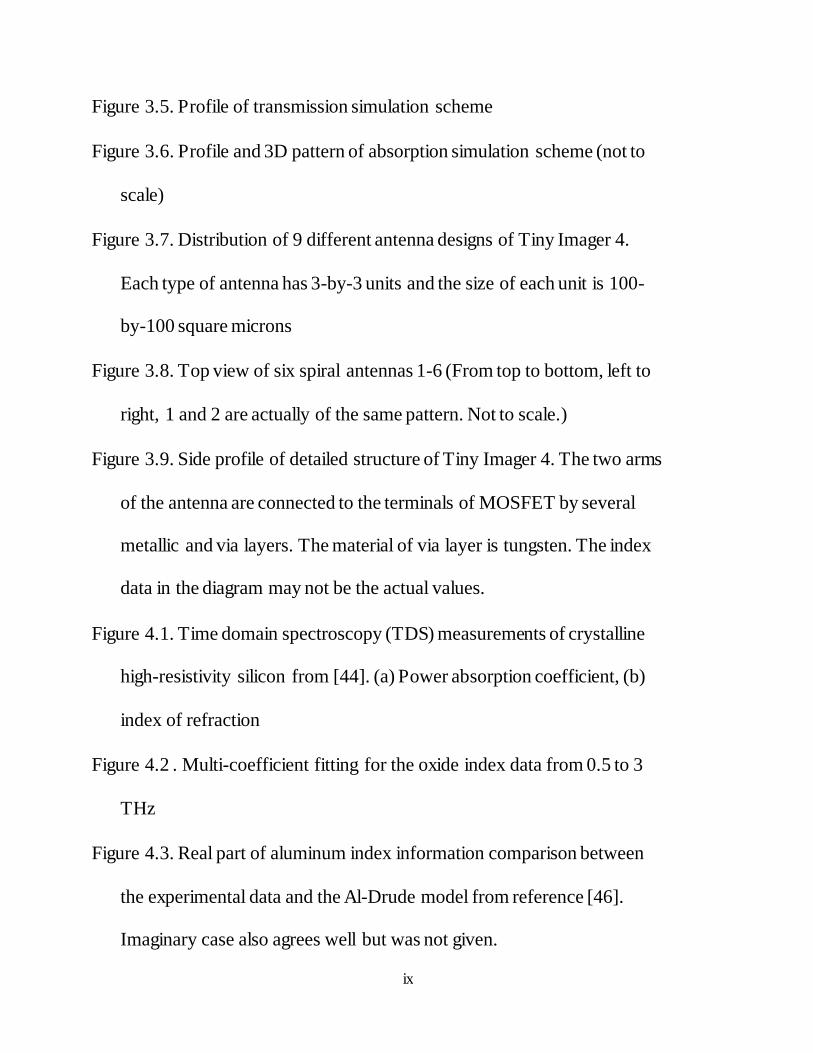
Figure 3.5. Profile of transmission simulation scheme
Figure 3.6. Profile and 3D pattern of absorption simulation scheme (not to
scale)
Figure 3.7. Distribution of 9 different antenna designs of Tiny Imager 4.
Each type of antenna has 3-by-3 units and the size of each unit is 100-
by-100 square microns
Figure 3.8. Top view of six spiral antennas 1-6 (From top to bottom, left to
right, 1 and 2 are actually of the same pattern. Not to scale.)
Figure 3.9. Side profile of detailed structure of Tiny Imager 4. The two arms
of the antenna are connected to the terminals of MOSFET by several
metallic and via layers. The material of via layer is tungsten. The index
data in the diagram may not be the actual values.
Figure 4.1. Time domain spectroscopy (TDS) measurements of crystalline
high-resistivity silicon from [44]. (a) Power absorption coefficient, (b)
index of refraction
Figure 4.2 . Multi-coefficient fitting for the oxide index data from 0.5 to 3
THz
Figure 4.3. Real part of aluminum index information comparison between
the experimental data and the Al-Drude model from reference [46].
Imaginary case also agrees well but was not given.

x
Figure 4.4. Transmission, Reflection and their sum for Bowtie antenna 1
(left) and Bowtie antenna 3 (right) using PEC model
Figure 4.5. Comparisons of transmission (left) and reflection (right) results
between the three models for Bowtie antenna 1 (top) and Bowtie antenna 3
(bottom)
Figure 4.6. Microscopic images of fabricated devices of the spiral type with
different winding numbers (From the reference paper [50])
Figure 4.7. Transmission results of spiral antenna with winding number 3 (the
second one of Figure 4.6) from the reference (left, blue line is for simulation
and red line is for experiment) and from our simulation (right)
Figure 4.8. Figure 2 from [51], field intensity spectra in the gap of antennas
Figure 4.9. Transmission curve of cross antenna for vertical polarization
from [50]
Figure 4.10. Transmission (red) and absorption (black) curves of three
bowtie antennas (top left for Bowtie antenna 1, top right for Bowtie
antenna 2, bottom left for Bowtie antenna 3) with unit pixel to be 100-
by-100 square microns
Figure 4.11. Transmission curves of Bowtie antenna 1 with different
periods from 100 to 500 microns (horizontal and vertical periods are the
same)

xi
Figure 4.12. Absorption curves for two bowtie antennas (both with a 50-
ohm resistor) of different periods. The unit of period is micron. The
inner and outer widths of antennas are 1 and 3.1 microns. They have a
2-micron gap, the length of one arm are 18.6 and 33.2 microns
respectively.
Figure 4.13. Sketch of the Bowtie antenna mentioned in the report of the
French group [53]
Figure 4.14. Schematic of Fat Bowtie antenna modeled here
Figure 4.15. Absorption curves for fat bowtie antennas restricted within a circle
of which diameter is 150 microns
Figure 4.16. Absorption curves for fat bowtie antennas restricted within a circle
of which diameter is 200 microns
Figure 4.17. Absorption curves for fat bowtie antennas restricted within a circle
of which diameter is 250 microns
Figure 4.18. Linear equation fitting between the antenna diameter and resonant
wavelength. x is diameter of the fat bowtie antennas and y is the
corresponding resonant wavelengths.
Figure 4.19. Pixel photograph of French group design [53]
Figure 4.20. Four different incident polarizations
xii
Figure 4.21. Absorption curves of the fat bowtie antenna for different
polarizations
Figure 4.22. Transmission curves of Bowtie antenna 1 for two cases
(reducing period versus adding more antennas for periodic boundary
case) and their difference
Figure 4.23. Absorption curves of Bowtie antenna 1 for two cases (reducing
period versus adding more antennas for periodic boundary case) and
their difference
Figure 4.24. Absorption results for simulations checking the effect of periodic
boundary. Three simulations have 1*1, 2*2, 3*3 antennas/pixels within the
boundary respectively.
Figure 4.25. Absorption curves for Bowtie antenna 3 (except that the length is
changed to be 40 microns for one element) for different resistances
Figure 4.26. Side profile of antenna with the locations of the three monitors
indicated. Three monitors (M1, M2, M3) are put across the metal
contact to detect the E-field distribution information. Not to scale.
Figure 4.27. M1 E-field distribution. Unit of E field is V/m.
Figure 4.28. M2 E-field distribution. Unit of E field is V/m.
Figure 4.29. M3 E-field distribution. Unit of E field is V/m.

xiii
Figure 4.30. Absorption curves for Bowtie antenna 1 (pixel pitch is
100*100 square microns) of different aluminum thicknesses from 0.5 to
1.5 microns
Figure 5.1. Linear equation fitting between the antenna length and resonant
wavelength for first generation bowtie antennas
Figure 5.2. Schematic of one arm and central resistor for the 6 antenna designs.
Not to scale.
Figure 5.3. Absorption responses for antennas of different lengths
Figure 5.4. Absorption responses for antennas of different angles
Figure 5.5. Absorption responses for antennas of different gaps
Figure 5.6. Absorption response comparison between two different oxide
models
Figure 5.7. Absorption response comparison considering oxide and nitride
configuration
Figure 5.8. New definitions for the antenna gap and angle (not to scale)
Figure 5.9. Absorption for a new defined bowtie antenna with length=110
microns, angle=30 degrees and gap=10 microns
Figure 5.10. Test structures to check the slot effect. Here, only one arm of
the antenna is shown, where the etched slots are of several rectangles
xiv
inside the arm. The widths of the etched slots are 2, 5 and 10 microns
respectively.
Figure 5.11. Absorption simulations for antennas with test slots
Figure 5.12. Two tests for antennas with etched blocks. The sizes of the
blocks are 5*5, 30*40 square microns respectively.
Figure 5.13. The antenna design with open-end slots and its absorption
response. The width of the slots is 2 microns
Figure 5.14. The designs that satisfy the manufacture rule and after corners
are rounded
Figure 5.15. Comparison between solid antenna with sharp corners and slot
antenna with rounded corners
Figure 5.16. Electric field distribution @215GHz for the central plane of the
slot antenna with rounded corners (the antenna is along the horizontal
direction). Electrical field unit: V/m
Figure 5.17. 1-D electric field distribution. Electrical field unit: V/m
Figure 5.18. Field distribution for antennas with gap=5 microns and inner
width from 5 to 40 microns. Electrical field unit: V/m
Figure 5.19. Electric field distribution from reference [56]
Figure 5.20. Absorption responses when the gap is changed from 10 to 20
microns
xv
Figure 5.21. Electric field distribution of the central plane through the
antenna for variations of the gap between the two arms. Electrical field
unit: V/m
Figure 5.22. Two different configurations for the final antenna design with a
gap of 2 microns (not to scale)
Figure 5.23. Response comparison between two resistor configurations
Figure 5.24. E-field distribution (@215THz) in a highlighted area (yellow
dash line box) of Configuration 2. Electrical field unit: V/m
Figure 5.25. Current density distribution (@215THz) in the highlighted area
in Figure 5.24. Current density unit: A/m2
Figure 5.26. Two sets of antenna designs for 188GHz transmission
experiment. In the first set, there is a gap between two arms of the
antenna. Certain implant could be added to define an equivalent resistor.
In the second set, there is no equivalent resistor and the two arms are
directly connected with each other.
Figure 5.27. Transmission curves for two sets of antennas (left, the green
line represents location of 188GHz) and the transmission values at
188GHz (right)
Figure 5.28. Transmission and reflection of air/silicon interface for radiation
of different incident angles
xvi
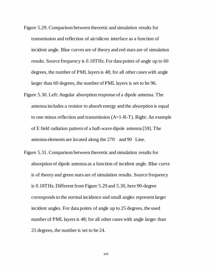
Figure 5.29. Comparison between theoretic and simulation results for
transmission and reflection of air/silicon interface as a function of
incident angle. Blue curves are of theory and red stars are of simulation
results. Source frequency is 0.18THz. For data points of angle up to 60
degrees, the number of PML layers is 48; for all other cases with angle
larger than 60 degrees, the number of PML layers is set to be 96.
Figure 5.30. Left: Angular absorption response of a dipole antenna. The
antenna includes a resistor to absorb energy and the absorption is equal
to one minus reflection and transmission (A=1-R-T). Right: An example
of E field radiation pattern of a half-wave dipole antenna [59]. The
antenna elements are located along the 270。 and 90。Line.
Figure 5.31. Comparison between theoretic and simulation results for
absorption of dipole antenna as a function of incident angle. Blue curve
is of theory and green stars are of simulation results. Source frequency
is 0.18THz. Different from Figure 5.29 and 5.30, here 90-degree
corresponds to the normal incidence and small angles represent larger
incident angles. For data points of angle up to 25 degrees, the used
number of PML layers is 48; for all other cases with angle larger than
25 degrees, the number is set to be 24.

xvii
List of Tables
Table 4.1. Resonant frequency/wavelength information for fat bowties of
three different diameters
Table 5.1. Resonant frequency information for the three bowtie antennas of
the first generation. The first row is length for one arm of the antenna.
Since the gap between the two arms is 2 microns, the antenna length (the
second row) is two times the values in the first row and then plus the
gap.
Table 5.2. Geometric parameters of the 6 antenna designs for the modeling
Table 5.3. Antenna parameters for 188GHz transmission experiment.
Period indicates the size of one pixel pitch. Array represents the
number of antennas in x and y directions (the array size of each type
of antenna is about 1.5*1.5 square centimeters).
1
1. Introduction
1.1 Terahertz radiation
Terahertz radiation (THz), or T-ray, generally refers to electromagnetic waves with
frequencies between 0.1 to 10 THz (wavelength: 30 to 3000 microns, energy: 0.4 to 40
meV) [1]. Terahertz waves locate itself between the traditional research regimes of
electronics and photonics in the electromagnetic spectrum, microwave and infrared to be
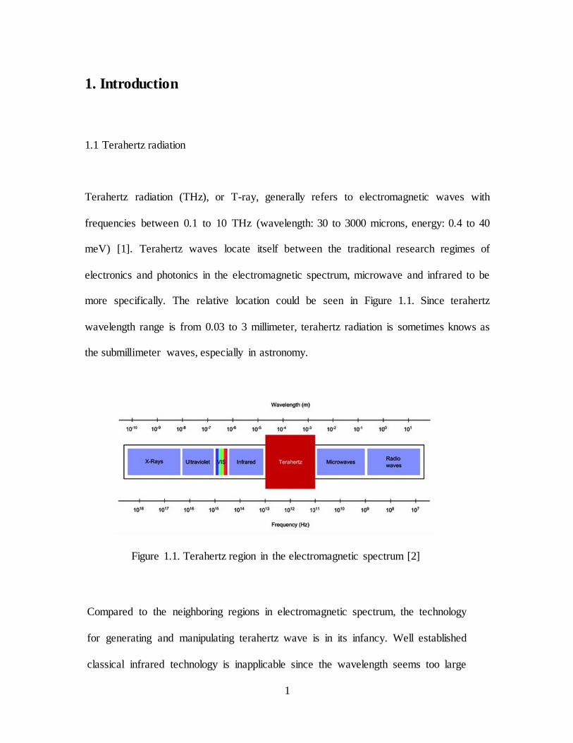
more specifically. The relative location could be seen in Figure 1.1. Since terahertz
wavelength range is from 0.03 to 3 millimeter, terahertz radiation is sometimes knows as
the submillimeter waves, especially in astronomy.
Figure 1.1. Terahertz region in the electromagnetic spectrum [2]
Compared to the neighboring regions in electromagnetic spectrum, the technology
for generating and manipulating terahertz wave is in its infancy. Well established
classical infrared technology is inapplicable since the wavelength seems too large
2
from the optical perspective. Also, similarly, the expertise at lower frequencies is
useless because the wavelength is small for that case. Hence, new devices and
techniques need to be developed for the ‘Terahertz Gap’. Fortunately, the last
decades have observed the most intense research work into this regime [3-7].
The motive to explore this less developed area is rather because of some uniquely
attractive features of terahertz waves than just simply closing the ‘Terahertz Gap’.
The property of terahertz waves can be seen in Section 1.2.
1.2. Properties of Terahertz Waves
Terahertz wave has some remarkable properties which would lead to valuable
applications in various fields. This section elaborates on these properties to offer
perspective for the subsequent terahertz applications.
1.2.1. Non-ionizing radiation
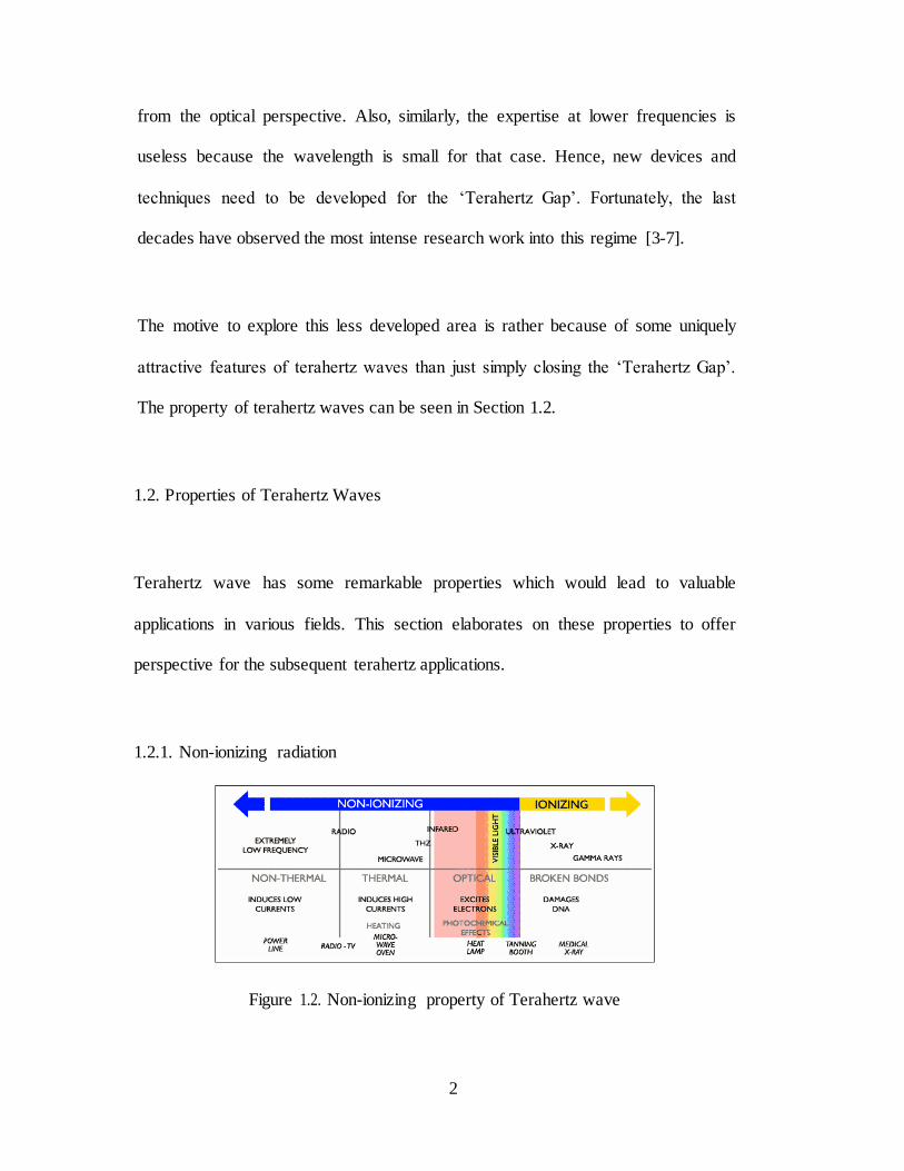
Figure 1.2. Non-ionizing property of Terahertz wave

3
Terahertz wave is non-ionizing radiation, indicating that its quantum does not have
enough energy to free electrons from an atom or molecule during interaction with a tissue
or material. It is intuitive that waves with larger frequency would have more power levels
and therefore could be ionizing and destructive. A well-known example of ionizing
radiation is x-ray. It is a concern that large does or frequent exposure to x-ray may result
in mutation, cancer or even death. Observing Figure 1.2, THz radiation has longer
wavelength and hence belongs to the safe region. This feature makes Terahertz a
potential alternative for the diagnosis and treatment to replace x-ray screening.
1.2.2. Terahertz penetration and transmission
Another primary advantage of terahertz wave is that many common materials and living
tissues are transparent or semi-transparent to light in this range [8]. Terahertz radiation
can penetrate through some non-conducting materials, like cloth, paper, wood, plastic and
ceramics, which may otherwise be opaque for radiation at other frequencies. Moreover,
many subjects feature characteristic absorption lines, therefore making it possible to do
identification by observing the Terahertz fingerprints.

4
Figure 1.3. Absorption spectra of different explosives (left) and other substances (right)
measured at THz frequencies [9]
An important obstacle for terahertz detection is that terahertz wave has limited
penetration through fog and cloud and can not penetrate liquid water or metal [10]. Figure
1.4 shows a measurement example for the atmospheric transmission. For space-based
detector, this effect would go away and would not be a concern. Otherwise, it should be
carefully considered.
Figure 1.4. Measured and simulated transmission spectra for a THz path length of 0.45m
at an ambient temperature of 20 degree centigrade and 30% humidity [11]
5
1.2.3. Some other terahertz wave properties
For one imaging system, according to the Rayleigh criterion, the minimum resolvable
angle of a circular aperture is proportional to the wavelength and is inversely proportional
to the diameter of the aperture. Therefore, compared to the current popular millimeter
wave scanner device, one system utilizing the terahertz wave could have much better
resolution and could be manufactured to be very compact. On the other hand, although
the traditional optical imaging system, like x-ray device, has finer resolution, penetration
characteristics as well as photon energy should also be taken into account. Sub-
wavelength resolution could also be achieved [12].
Also, considering that Rayleigh scattering intensity is inversely proportional to the
fourth power of the wavelength, THz wave scatters less than that of the optical
radiation (optical section has shorter wavelength). This is favorable to get an image
with better image quality.
1.3. Applications of Terahertz radiation
After reviewing the properties of the terahertz range radiation in the last part, here
we tend to have a look at some practical applications.
1.3.1. Security
6
As mentioned in the penetration characteristics of terahertz wave, this radiation
could pass through fabric, plastic, cloth, etc. This feature makes it ideal for
surveillance applications, for example, safety check at airports or government
buildings. Terahertz imaging system is able to ‘see’ forbidden and hidden objects
remotely. This is of particular interest since the travel flow keeps increasing and
THz waves have better a resolution. Also, considering that terahertz radiation has a
high chemical sensitivity or many chemical/biological subjects have specific
terahertz fingerprints, it is great to combine terahertz spectroscopy technique to
detect the composite of certain item concealed in a container. This is a very
promising application to replace the existing mm-wave and x-ray scanner systems in
that it provides better penetration, better resolution, no harm to human tissue and do
not need to have contacts to the examined subject.
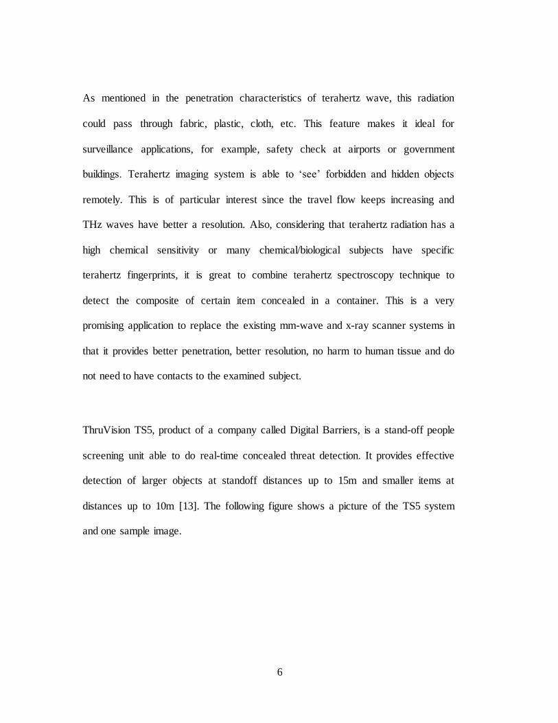
ThruVision TS5, product of a company called Digital Barriers, is a stand-off people
screening unit able to do real-time concealed threat detection. It provides effective
detection of larger objects at standoff distances up to 15m and smaller items at
distances up to 10m [13]. The following figure shows a picture of the TS5 system
and one sample image.
7
Figure 1.5. ThruVision TS5 people screening system (upper) and Weapon detection
of a person with a hammer [13]
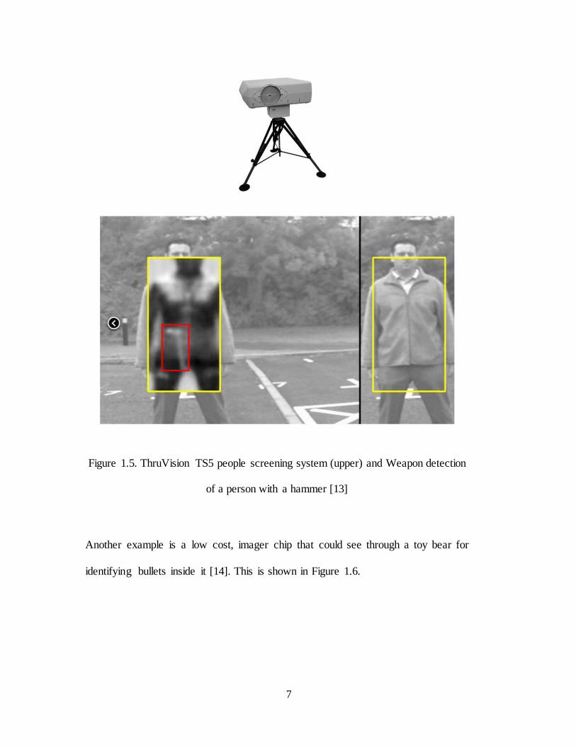
Another example is a low cost, imager chip that could see through a toy bear for
identifying bullets inside it [14]. This is shown in Figure 1.6.
8
Figure 1.6. A tiny terahertz detection device detecting the hidden bullets inside a toy
bear [14]
1.3.2. Terahertz spectroscopy identification
Spectroscopy results of terahertz radiation are able to provide novel information in
chemistry and biochemistry. Many materials have feature absorption lines in the
terahertz range, facilitating the identification or differentiation by the spectral
responses. This is also helpful in terms of mail/package screening since people
become more worried there may be some dangerous substance that may threaten
receiver’s health.
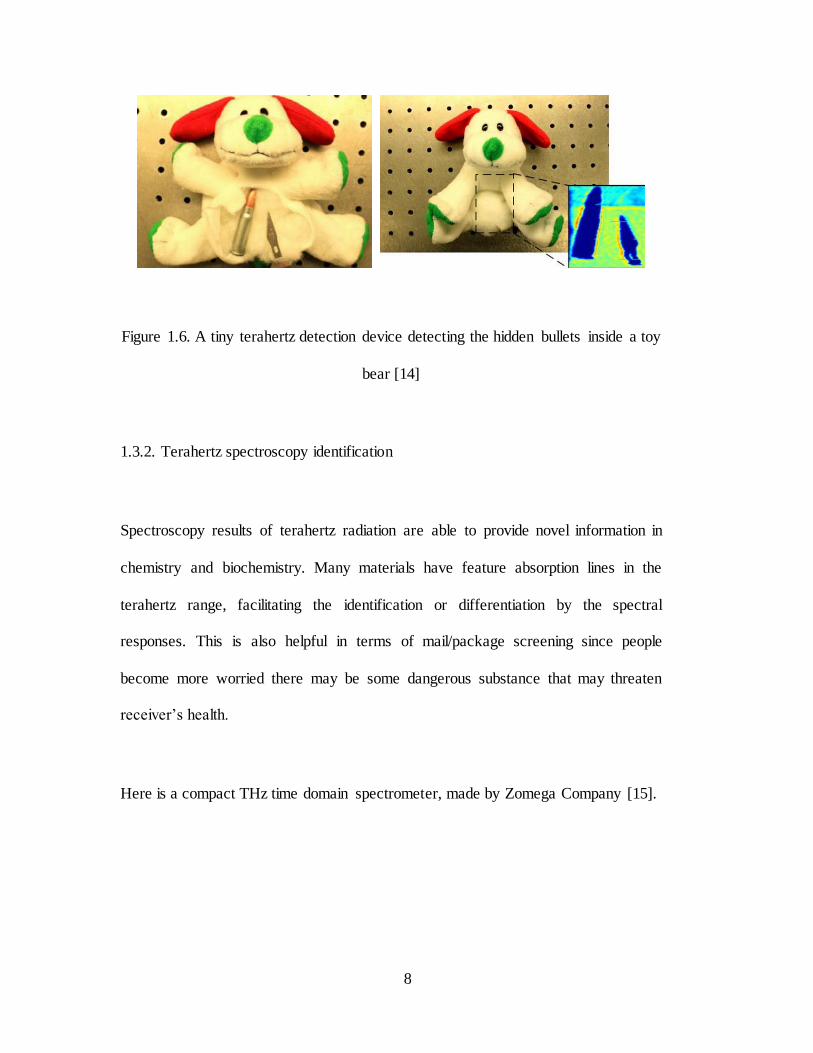
Here is a compact THz time domain spectrometer, made by Zomega Company [15].
9
Figure 1.7. Mini-Z THz Time Domain Spectrometer [15]
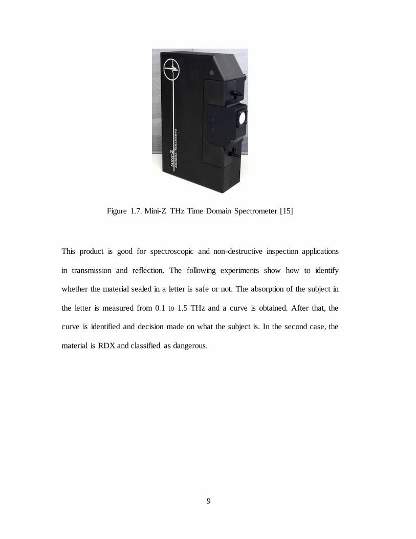
This product is good for spectroscopic and non-destructive inspection applications
in transmission and reflection. The following experiments show how to identify
whether the material sealed in a letter is safe or not. The absorption of the subject in
the letter is measured from 0.1 to 1.5 THz and a curve is obtained. After that, the
curve is identified and decision made on what the subject is. In the second case, the
material is RDX and classified as dangerous.
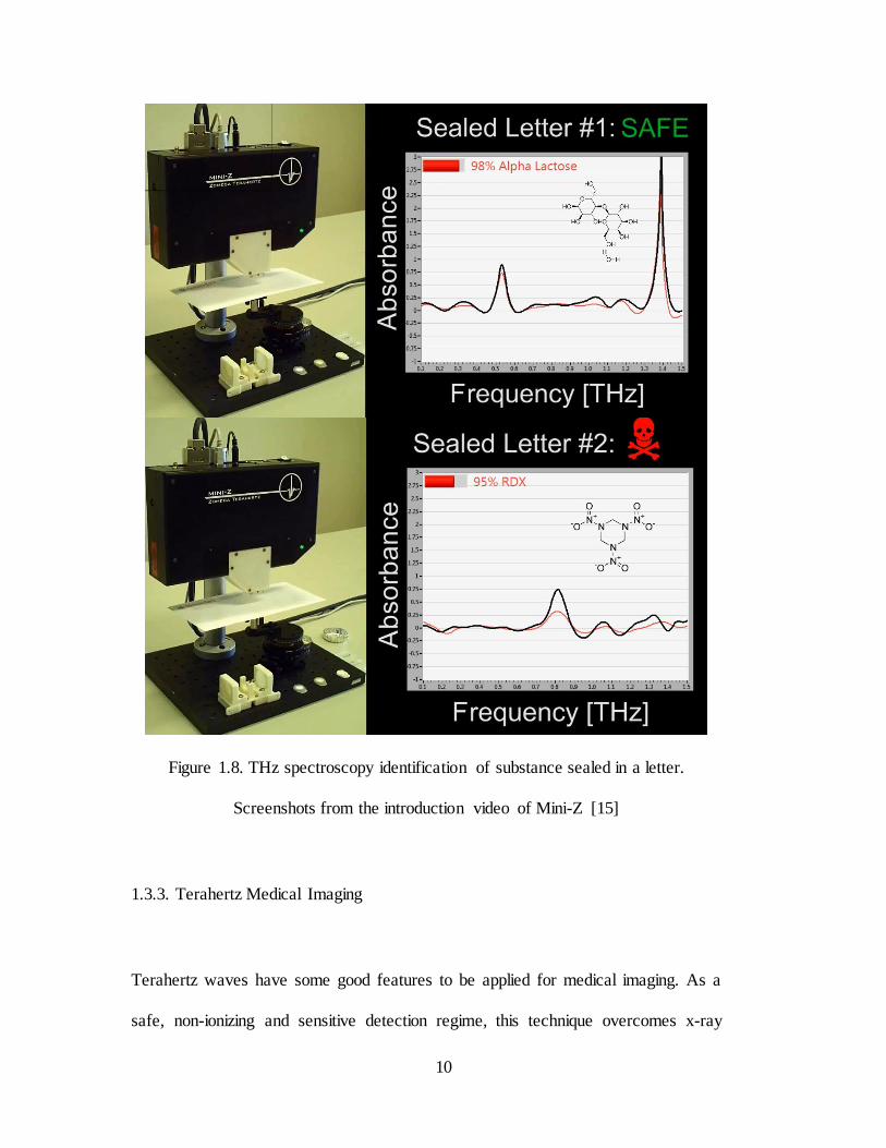
10
Figure 1.8. THz spectroscopy identification of substance sealed in a letter.
Screenshots from the introduction video of Mini-Z [15]
1.3.3. Terahertz Medical Imaging
Terahertz waves have some good features to be applied for medical imaging. As a
safe, non-ionizing and sensitive detection regime, this technique overcomes x-ray
11
and CT scan for some aspects and may even replace them finally. Considering
terahertz’s ability to recognize spectral fingerprints, it could provide good contrast
between different types of soft tissues. Also, it is a sensitive method of detecting
water content and other markers of cancer. Due to strong water absorption, it could
only penetrate a small distance and allows high-resolution subsurface imaging of
tissue.
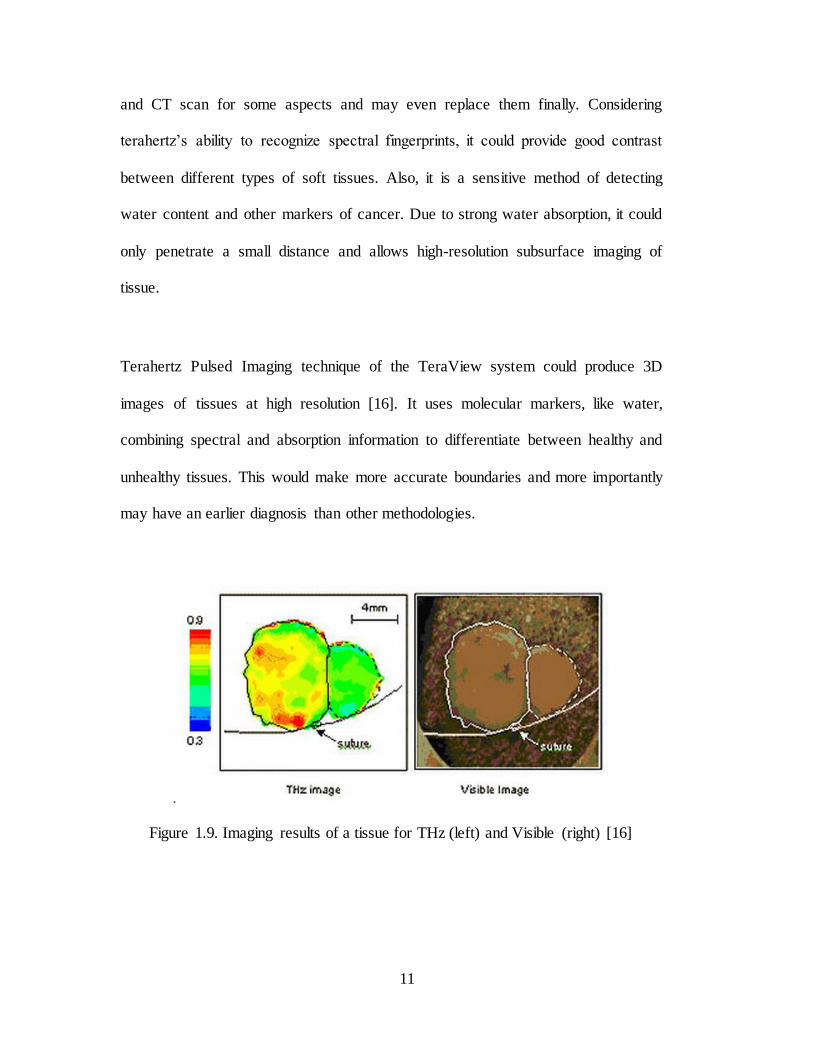
Terahertz Pulsed Imaging technique of the TeraView system could produce 3D
images of tissues at high resolution [16]. It uses molecular markers, like water,
combining spectral and absorption information to differentiate between healthy and
unhealthy tissues. This would make more accurate boundaries and more importantly
may have an earlier diagnosis than other methodologies.
Figure 1.9. Imaging results of a tissue for THz (left) and Visible (right) [16]
12
The difference between these two images is that it is much easier for the observer to
distinguish cancerous and non-cancerous cells in the first one while the second one
seems more uniform. This application is definitely meaningful for that early
detection would greatly increase the likelihood of cure.
1.3.4. Some other applications
For communication application, since terahertz radiation was not fully understood
so it has the potential for the broadband wireless communication [17]. Another
factor is that the use should be applied at higher altitude for the water vapor at lower
altitude would greatly absorb the signal. The usefulness in long-distance
communication is restricted. However, in relatively short distances, this band
exhibits valuable applications in imaging and wireless networking systems [18].
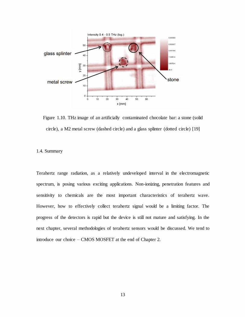
In the manufacturing industry, THz systems could do the quality control and the process
monitoring job. This is based on the transparent property of the packaging materials to
terahertz waves. Therefore, terahertz is able to detect the defects residing in the
transparent materials which would not be detectable for sources of some other
frequencies. For the following example, three defects could be easily detected by the THz
image [19].
13
Figure 1.10. THz image of an artificially contaminated chocolate bar: a stone (solid
circle), a M2 metal screw (dashed circle) and a glass splinter (dotted circle) [19]
1.4. Summary
Terahertz range radiation, as a relatively undeveloped interval in the electromagnetic
spectrum, is posing various exciting applications. Non-ionizing, penetration features and
sensitivity to chemicals are the most important characteristics of terahertz wave.
However, how to effectively collect terahertz signal would be a limiting factor. The
progress of the detectors is rapid but the device is still not mature and satisfying. In the
next chapter, several methodologies of terahertz sensors would be discussed. We tend to
introduce our choice – CMOS MOSFET at the end of Chapter 2.
14
2. MOSFET detection
Research on terahertz detectors is a significant section of work to close the ‘Terahertz
Gap’ and is driving the entire field to develop to gain capabilities comparable to the
sensors like in the infrared (IR) region. Here we first introduce several popular types of
terahertz detectors and then elaborate on the MOSFET methodology.
2.1. Direct and heterodyne THz detection
Generally, all the radiation detection systems for THz could be divided into two
categories: incoherent and coherent. Incoherent systems use direct detection sensors,
which only collect signal amplitude information and are broadband detection devices;
coherent systems utilize heterodyne circuit design which allows not only the amplitude
but also phase of the signal to be collected. For the heterodyne design, radiation of high
frequency where there are no proper amplifiers is transferred to much lower frequencies
and then amplified by low-noise amplifiers. These systems are for narrow-band detection
[20].
15
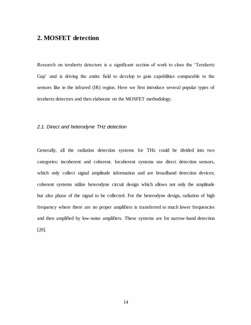
Figure 2.1. Schematic representation of a direct detection. WS is the signal power and WB
is the background radiation power. [20]
Figure 2.1 shows a schematic diagram for the direct detection. The detector collects both
signal and background radiation power. Optics focuses the incident radiation and
transfers it to the detector and a filter before detector would remove the background
radiation out of the interested wavelength band. A small signal will be amplified and the
resulting IS be further processed.
For direct THz detection, room temperature detector could be achieved with relatively
longer response time and modest sensitivity. However, some cooled semiconductor
detectors [20] response much quicker and have much lower NEP.
The advantage of direct detection systems is its simplicity and the possibility to design
large arrays [21-25]. Therefore, most imaging systems use passive direct detection.
16
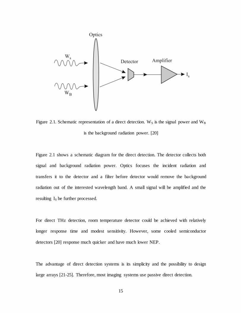
In heterodyne detectors, THz signals are down-converted to intermediate frequency (IF)
while the amplitude and phase information of the original radiation are preserved.
Figure 2.2. Schematic representation of heterodyne detection
In the above figure, there is a radiant power WLO (to drive the mixing process) from a
local oscillator in addition to the signal and background radiation power. The mixer
aligns WS and WLO and generates a signal of intermediate frequency (the difference of
signal and local oscillator frequencies). The IF signal is then amplified and processed.
The heterodyne overcomes direct detection in that it converts the signal frequency to a
lower intermediate frequency, which is appropriate to electronics time response. Also, it
has higher spectral resolution. When background radiation is low, direct detection,
operating in wider spectral range, could provide decent resolution. Direct detection is
preferable for imaging [26] and can be used in applications where sensitivity is more
17
important than spectral resolution. In active (the scene is illuminated) systems,
heterodyne detection could be used to increase sensitivity.
2.2. Photon and thermal detectors
Based on the mechanism of detection, terahertz detectors are mainly divided into two
groups: photon detectors and thermal detectors.
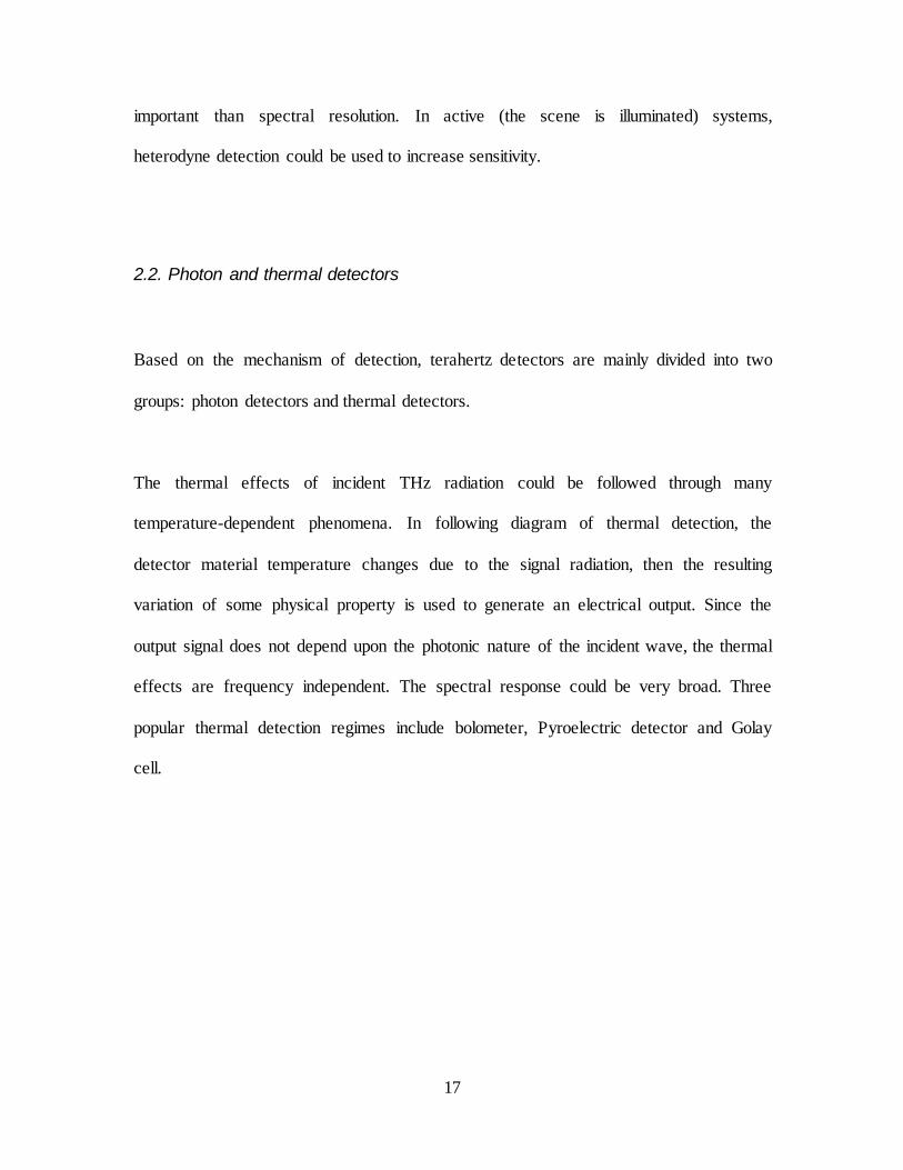
The thermal effects of incident THz radiation could be followed through many
temperature-dependent phenomena. In following diagram of thermal detection, the
detector material temperature changes due to the signal radiation, then the resulting
variation of some physical property is used to generate an electrical output. Since the
output signal does not depend upon the photonic nature of the incident wave, the thermal
effects are frequency independent. The spectral response could be very broad. Three
popular thermal detection regimes include bolometer, Pyroelectric detector and Golay
cell.
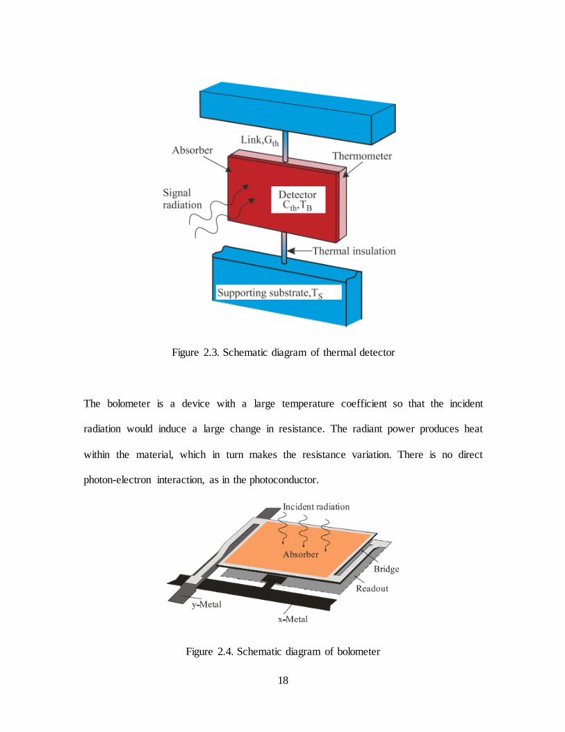
18
Figure 2.3. Schematic diagram of thermal detector
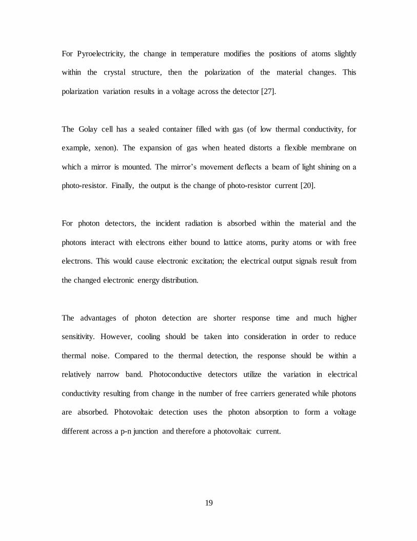
The bolometer is a device with a large temperature coefficient so that the incident
radiation would induce a large change in resistance. The radiant power produces heat
within the material, which in turn makes the resistance variation. There is no direct
photon-electron interaction, as in the photoconductor.
Figure 2.4. Schematic diagram of bolometer
19
For Pyroelectricity, the change in temperature modifies the positions of atoms slightly
within the crystal structure, then the polarization of the material changes. This
polarization variation results in a voltage across the detector [27].
The Golay cell has a sealed container filled with gas (of low thermal conductivity, for
example, xenon). The expansion of gas when heated distorts a flexible membrane on
which a mirror is mounted. The mirror’s movement deflects a beam of light shining on a
photo-resistor. Finally, the output is the change of photo-resistor current [20].
For photon detectors, the incident radiation is absorbed within the material and the
photons interact with electrons either bound to lattice atoms, purity atoms or with free
electrons. This would cause electronic excitation; the electrical output signals result from
the changed electronic energy distribution.
The advantages of photon detection are shorter response time and much higher
sensitivity. However, cooling should be taken into consideration in order to reduce
thermal noise. Compared to the thermal detection, the response should be within a
relatively narrow band. Photoconductive detectors utilize the variation in electrical
conductivity resulting from change in the number of free carriers generated while photons
are absorbed. Photovoltaic detection uses the photon absorption to form a voltage
different across a p-n junction and therefore a photovoltaic current.
20
Under certain circumstances, MOSFET (Metal Oxide Semiconductor Field Effect
Transistor) could be able to serve as a specific kind of photon detector for Terahertz
radiation. The characteristics and detection mechanisms of this detection will be
illustrated in the next section.
2.3. MOSFET detection
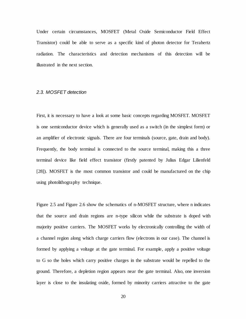
First, it is necessary to have a look at some basic concepts regarding MOSFET. MOSFET
is one semiconductor device which is generally used as a switch (in the simplest form) or
an amplifier of electronic signals. There are four terminals (source, gate, drain and body).
Frequently, the body terminal is connected to the source terminal, making this a three
terminal device like field effect transistor (firstly patented by Julius Edgar Lilienfeld
[28]). MOSFET is the most common transistor and could be manufactured on the chip
using photolithography technique.
Figure 2.5 and Figure 2.6 show the schematics of n-MOSFET structure, where n indicates
that the source and drain regions are n-type silicon while the substrate is doped with
majority positive carriers. The MOSFET works by electronically controlling the width of
a channel region along which charge carriers flow (electrons in our case). The channel is
formed by applying a voltage at the gate terminal. For example, apply a positive voltage
to G so the holes which carry positive charges in the substrate would be repelled to the
ground. Therefore, a depletion region appears near the gate terminal. Also, one inversion
layer is close to the insulating oxide, formed by minority carriers attractive to the gate
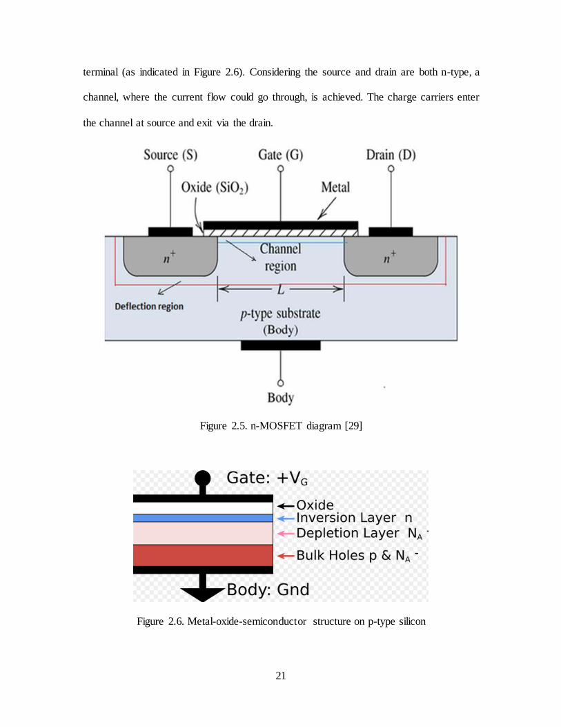
21
terminal (as indicated in Figure 2.6). Considering the source and drain are both n-type, a
channel, where the current flow could go through, is achieved. The charge carriers enter
the channel at source and exit via the drain.
Figure 2.5. n-MOSFET diagram [29]
Figure 2.6. Metal-oxide-semiconductor structure on p-type silicon
22
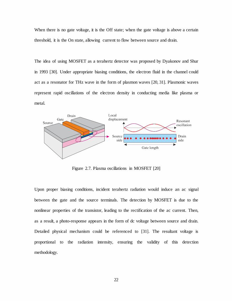
When there is no gate voltage, it is the Off state; when the gate voltage is above a certain
threshold, it is the On state, allowing current to flow between source and drain.
The idea of using MOSFET as a terahertz detector was proposed by Dyakonov and Shur
in 1993 [30]. Under appropriate biasing conditions, the electron fluid in the channel could
act as a resonator for THz wave in the form of plasmon waves [20, 31]. Plasmonic waves
represent rapid oscillations of the electron density in conducting media like plasma or
metal.
Figure 2.7. Plasma oscillations in MOSFET [20]
Upon proper biasing conditions, incident terahertz radiation would induce an ac signal
between the gate and the source terminals. The detection by MOSFET is due to the
nonlinear properties of the transistor, leading to the rectification of the ac current. Then,
as a result, a photo-response appears in the form of dc voltage between source and drain.
Detailed physical mechanism could be referenced to [31]. The resultant voltage is
proportional to the radiation intensity, ensuring the validity of this detection
methodology.
23
There are two operation modes for MOSFET terahertz detection: resonant (tuned to a
specific wavelength) and non-resonant (broadband). It is directly tunable by varying the
gate voltage [32-37]. When the channel length is short enough, a standing plasmon wave
could be formed in the channel facilitating signal amplification. In this case, the device
has a high responsivity due to the internal amplification and the response is narrow-band.
As the channel length becomes longer, the plasmon wave decays before it reaches the
other side of the channel. This detector operates in wide temperature range up to room
temperature [38,39]. However, at room temperature, electron mobility is too low to
support the resonant response to happen [31]. Therefore, in our testing setup, the
detection works for the non-resonant mode.
The advantages of using MOSFET terahertz detection include: commercialized CMOS
fabrication industry makes the manufacture of low cost and high yield; low NEP for room
temperature operation; we could make a very compact detector array to achieve frame
imaging; lastly, a significant progress in sensitivity could be obtained by introducing an
antenna to help couple terahertz radiation to the small absorption element of detector.
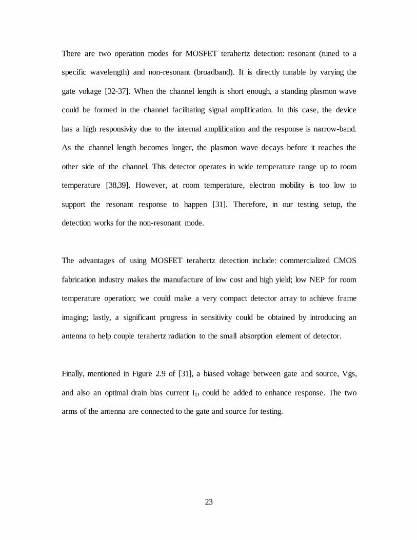
Finally, mentioned in Figure 2.9 of [31], a biased voltage between gate and source, Vgs,
and also an optimal drain bias current ID could be added to enhance response. The two
arms of the antenna are connected to the gate and source for testing.
24
Figure 2.8. MOSFET THz detection with biased voltage, however, the biased current
between source and drain is not included
The main focus of this thesis is modeling and optimal design of the coupling antenna,
which is part of the work to enhance the signal of the whole detection system. The
remaining of the thesis will talk about the work related to the antenna design.
25
3. Numerical method, realization and simulation model
The subject of this thesis is to simulate terahertz antenna and to optimize the antenna
design based on the modeling results. This chapter talks about the numerical method used
to do simulation, the corresponding software to realize the simulation and details of the
model.
3.1. Finite Difference Time Domain method
Our numerical simulations are based on FDTD method. Therefore, here we first
have a brief review of what FDTD method is.
Finite Difference Time Domain is a numerical calculation tool based on Maxwell
equations and is used for modeling computational electrodynamics. The most
significant feature of this method is that it is a time domain method; therefore the
response results of the simulation could cover a wide range of frequencies with a
single run.
26
Figure 3.1. Illustration of a standard Cartesian Yee cell in FDTD method. It is noted that
the electric and magnetic vectors are discretized in space. Also, they are derived
alternatively in time.
FDTD method belongs to grid based calculation techniques. Maxwell equations are
discretized using central-difference approximations to the space and time partial
derivatives. Here is an example in vacuum for the plane wave situation (electric and
magnetic fields are along x and y directions respectively, the wave propagates along
z direction):
1/2 1/2
0
( 1/ 2) ( 1/ 2)( ) ( ) 1n nn ny yx x
H k H kE k E k
t x (3.1)
1 1/2 1/2
0
( 1/ 2) ( 1/ 2) ( 1) ( )1n n n ny y x x
H k H k E k E k
t x (3.2)
In these two equations, superscript is time and n represents a time that is t t n .
The variable in the parenthesis is space and k represents a location that is z x k .
27
The two equations assume that E and H are separated in both time and space
domains. The above equations could be arranged to arrive at the following:
1/2 1/2
0
( ) ( ) [ ( 1/ 2) ( 1/ 2)]n n n n
x x y y
tE k E k H k H k
x (3.3)
1 1/2 1/2
0
( 1/ 2) ( 1/ 2) [ ( 1) ( )]n n n n
y y x x
tH k H k E k E k
x (3.4)
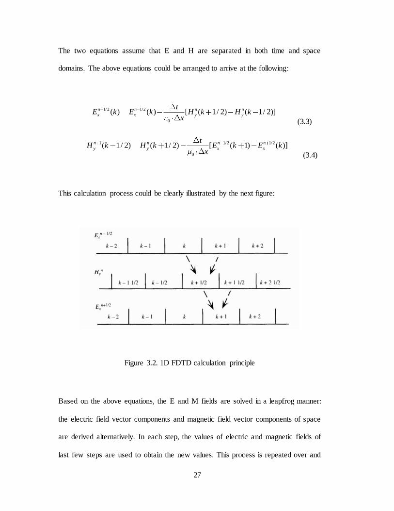
This calculation process could be clearly illustrated by the next figure:
Figure 3.2. 1D FDTD calculation principle
Based on the above equations, the E and M fields are solved in a leapfrog manner:
the electric field vector components and magnetic field vector components of space
are derived alternatively. In each step, the values of electric and magnetic fields of
last few steps are used to obtain the new values. This process is repeated over and
28
over again until arriving at a steady state. The fundamental and most important idea
of FDTD method could be well indicated by the above figure.
Since FDTD method proposes few approximations or simplifications from the
starting point of Maxwell equations, it is an accurate and powerful method to predict
the electromagnetic behavior of specific structures as long as the index parameters
of the materials are known. This technique is very popular in nano-science world
and could be well utilized to analyze some terahertz instrumentations.
The weak point is that in order to get acceptable accuracy, the grid must be set to be
fine enough to resolve the smallest wavelength and geometrical feature in the
model, which substantially increases the calculation burden. Since FDTD requires
the entire simulation region to be gridded, the setup of mesh size is an important
factor to affect the calculation efficiency. In fact, Lumerical, the software we use,
implements a regime to address this issue, which will be mentioned in the next part.
3.2. Lumerical FDTD Solutions
FDTD Solutions is an FDTD-method Maxwell solver package for the design,
analysis and optimization of nanophotonic devices, processes and materials. It is
developed by Lumerical, a company headquartered in Vancouver, Canada. [40]
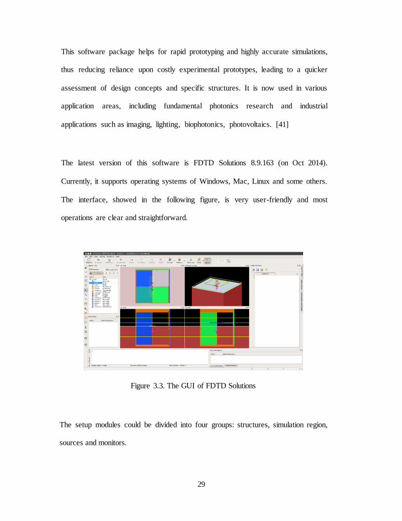
29
This software package helps for rapid prototyping and highly accurate simulations,
thus reducing reliance upon costly experimental prototypes, leading to a quicker
assessment of design concepts and specific structures. It is now used in various
application areas, including fundamental photonics research and industrial
applications such as imaging, lighting, biophotonics, photovoltaics. [41]
The latest version of this software is FDTD Solutions 8.9.163 (on Oct 2014).
Currently, it supports operating systems of Windows, Mac, Linux and some others.
The interface, showed in the following figure, is very user-friendly and most
operations are clear and straightforward.
Figure 3.3. The GUI of FDTD Solutions
The setup modules could be divided into four groups: structures, simulation region,
sources and monitors.
30
The first one, structures, is to define the physical structure of the research object.
This could be done either from internal models or from imported external files. In
our case, we sometimes need to import GDSII files for the antenna design. In this
step, the index data of all materials involved in the simulation should be defined.
Several material models and many experimental databases are provided. However,
if those are still not satisfying, we can define whatever is desired.
After that, the simulation regions are defined. One general area is mandatory while
mesh override regions are optional, there could be more than one override regions.
The size, boundary condition, mesh size of the region are the fundamental
parameters. And usually, in order to save the required memory while maintaining
certain accuracy, several sub-regions could be set to have finer meshes. The most
common boundary conditions are Perfect Matched Layer--PML, Metal, Periodic,
Bloch, symmetric and anti-symmetric. In our simulations, Periodic condition is
chosen, which will be discussed later.
The sources part describes the type of incident radiation and related parameters.
Different types are dipole, Gaussian, plane wave, total field scattered field and some
others. For a plane wave that covers a certain bandwidth, the software optimizes a
pulse in time domain to contain all the interested frequencies.
Monitors are for collecting and analyzing data. Two important and straightforward
ones are frequency-domain field profile monitor/frequency-domain field and power
31
monitor. The former is used to record the field distribution while the latter could
collect information like transmission and reflection through a specific plane.
We feel grateful that we are authorized to utilize research computing resources both
from Odyssey high performance cluster at Harvard University and Bluehive2 cluster
at University of Rochester. Odyssey has a total of 54000 CPUs, 2140 nodes, 190 TB
of RAM, and over 10 PB of storage [42]. BlueHive2 consists of approximately 200
compute nodes, with 2 x 12-core Intel "Ivy Bridge" CPUs per node and up to 512
GB of memory per node [43]. Both of these two clusters use SLURM as the queue
manager.
3.3. Simulation model
In this part, details of our model in FDTD Solutions to simulate
transmission/absorption are to be illustrated.
The MOSFET detector is so small compared to the wavelength of terahertz waves
(several microns to hundreds of microns). Therefore, a larger antenna is needed to
couple as more incident energy as possible for certain interested spectral bands.
Two types of antennas are considered: bowtie and spiral. Each antenna contains two
elements/arms. Examples of their schematics are shown in the following figure.
32
Figure 3.4. Top view of a bowtie antenna (left) and a spiral antenna (right) we try to
model (not to scale)
In practice, antennas are made of aluminum and are sitting on silicon substrate (also
an oxide layer may be present, not shown here). For calculating transmission, the
whole structure is illustrated in Figure 3.5. A plane wave source propagates from
top to bottom. Two power monitors are put above and below the interface in order
to collect data of how much energy is reflected or transmitted.

33
Figure 3.5. Profile of transmission simulation scheme
For most of the time, we use periodic boundary conditions along both x and y
directions (light propagates along z direction), including only one unit antenna in
the simulation region. This is equivalent to an infinite array of repeating antennas in
the x-y plane. For z direction, Perfect Matched Layer (PML) conditions are chosen
and distances from boundary to the antenna/substrate interface are at least half of the
wavelength of radiation. An override grid region contains the antenna, making the
mesh around finer for higher accuracy.
In fact, the transmission monitor should not be in the substrate. However, in order to
eliminate the etalon effect of the substrate, the monitor now is placed in the
substrate. Some discussion about this fact will be seen in section 4.2.
Pla
ne w ave sou
Ref
lection
Tran
smission
Ant
enna
Su
bstrate
34
The goal of the antenna is to transfer more incident THz energy to the detector.
However, in the transmission scheme, no element is in charge of absorption
considering that aluminum in terahertz range could be approximated as perfect
electrical conductor (section 4.1). Actually, the two arms of the antenna are
connected to two terminals of a MOSFET. FDTD Solutions is an optical simulation
software so it could not characterize doped silicon area unless we have knowledge
of how the doping will affect the refractive index of the material. Here, a simple
idea is proposed (Figure 3.6). Two elements of the antenna are connected to a
resistor (responsible for absorption) via metal contact. The default set is: the
thickness of antenna, metal contact and resistor is one micron. The material of
antenna and metal contact is perfect electrical conductor. The resistor is set to be
‘conductive’ type of material in Lumerical and the resistance could be adjusted by
changing its conductivity. For example, for one bowtie antenna, the resistor is a 6
microns long, 1 micron wide and 1 micron thick block with its conductivity set to be
120000 (ohm ·m) -1
. Thus its equivalent resistance is equal to a default value, 50
ohms. Finally, absorption by the resistor (or the whole system) is derived by one
minus transmission and reflection (A=1-T-R).
Absorption = 1 – Transmission – Reflection (3.5)

35
Figure 3.6. Profile and 3D pattern of absorption simulation scheme (not to scale)
While we test various antennas, we may focus on what have already been
manufactured. Tiny Imager 4, shown in Figure 3.7, is the first generation chip
(manufactured by MOSIS and was under joint project with ITT Exelis and CEIS at
University of Rochester) we have, including antenna and the underlying electrical
parts. The three bowtie antennas and six spiral antennas were designed by ITT
Exelis and the GDS II format designs were loaded in FDTD Solutions. Each type of
antenna has 3-by-3 units and the size of each unit is 100-by-100 square microns
(Antenna array are densely packed for absorbing more incident radiation).
Polarization of incident light is set to be horizontal (x direction in the following
c
ontacts
T
op view

36
figure). For convenience, these nine antennas are noted as ‘Bowtie antenna 1-3’ and
‘Spiral antenna 1-6 (actually 1 and 2 are the same one)’ in the following content.
Figure 3.7. Distribution of 9 different antenna designs of Tiny Imager 4. Each type
of antenna has 3-by-3 units and the size of each unit is 100-by-100 square microns
The geometric parameters of the bowtie antennas are:
a. Bowtie antenna 1
Inner width: 1 micron; Outer width: 5.7 microns; Gap: 2 microns
Length of one element: 33.2 microns; Total length of one antenna: 68.4 microns
b. Bowtie antenna 2
Inner width: 1 micron; Outer width: 3.3 microns; Gap: 2 microns
Length of one element: 18.8 microns; Total length of the antenna: 39.6 microns
c. Bowtie antenna 3
Inner width: 1 micron; Outer width: 8.1 microns; Gap: 2 microns
37
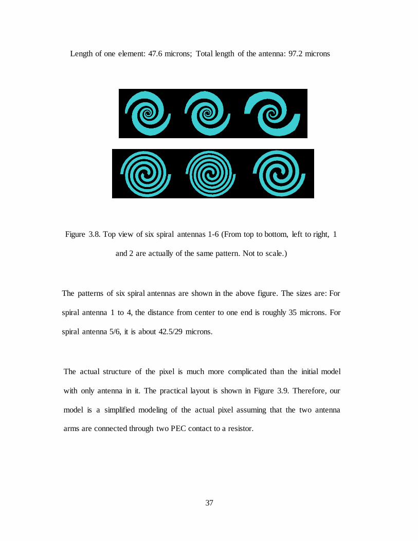
Length of one element: 47.6 microns; Total length of the antenna: 97.2 microns
Figure 3.8. Top view of six spiral antennas 1-6 (From top to bottom, left to right, 1
and 2 are actually of the same pattern. Not to scale.)
The patterns of six spiral antennas are shown in the above figure. The sizes are: For
spiral antenna 1 to 4, the distance from center to one end is roughly 35 microns. For
spiral antenna 5/6, it is about 42.5/29 microns.
The actual structure of the pixel is much more complicated than the initial model
with only antenna in it. The practical layout is shown in Figure 3.9. Therefore, our
model is a simplified modeling of the actual pixel assuming that the two antenna
arms are connected through two PEC contact to a resistor.
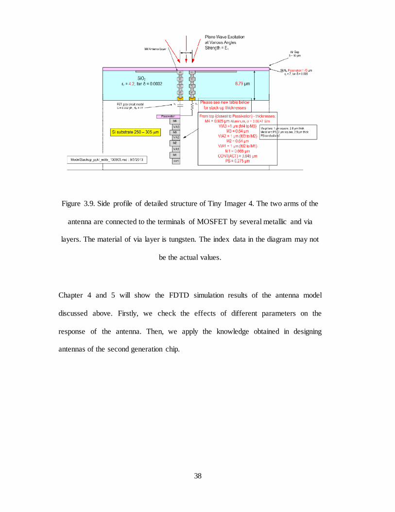
38
Figure 3.9. Side profile of detailed structure of Tiny Imager 4. The two arms of the
antenna are connected to the terminals of MOSFET by several metallic and via
layers. The material of via layer is tungsten. The index data in the diagram may not
be the actual values.
Chapter 4 and 5 will show the FDTD simulation results of the antenna model
discussed above. Firstly, we check the effects of different parameters on the
response of the antenna. Then, we apply the knowledge obtained in designing
antennas of the second generation chip.
39
4. Effects of different parameters on the antenna performance
In this chapter, we have various tests to check effects of different parameters on the
antenna frequency response. The parameters include material index data, pixel density,
boundary condition, antenna resistance, antenna shape, etc. Also, some simulation results,
like the field distribution would provide better understanding of how the antenna works.
Some comparisons between our results and references are made to make sure that our
simulation is valid.
4.1. Material index
Since terahertz is a relatively unexplored field, characteristics of the materials in this
range have not been well studied or measured compared with those in some other
spectral bands. Moreover, choosing an appropriate index model may greatly
promote the computational efficiency. In FDTD modeling, index information of
every mesh point should be clearly defined. Here, parameters of all the materials
used in the simulation are illustrated.
For silicon substrate, the data in [44] are used. The silicon samples measured in the
reference were of float-zone material (very pure silicon obtained by vertical zone
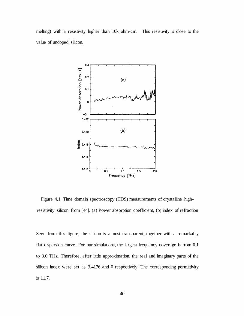
40
melting) with a resistivity higher than 10k ohm-cm. This resistivity is close to the
value of undoped silicon.
Figure 4.1. Time domain spectroscopy (TDS) measurements of crystalline high-
resistivity silicon from [44]. (a) Power absorption coefficient, (b) index of refraction
Seen from this figure, the silicon is almost transparent, together with a remarkably
flat dispersion curve. For our simulations, the largest frequency coverage is from 0.1
to 3.0 THz. Therefore, after little approximation, the real and imaginary parts of the
silicon index were set as 3.4176 and 0 respectively. The corresponding permittivity
is 11.7.
41
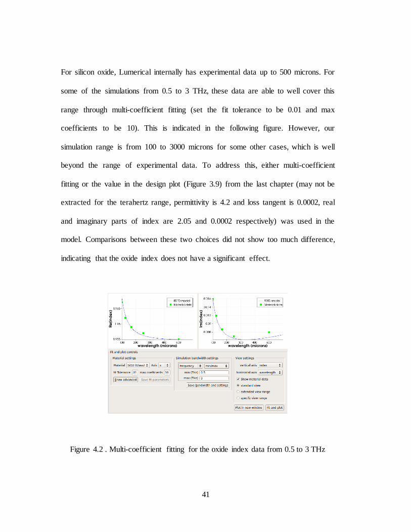
For silicon oxide, Lumerical internally has experimental data up to 500 microns. For
some of the simulations from 0.5 to 3 THz, these data are able to well cover this
range through multi-coefficient fitting (set the fit tolerance to be 0.01 and max
coefficients to be 10). This is indicated in the following figure. However, our
simulation range is from 100 to 3000 microns for some other cases, which is well
beyond the range of experimental data. To address this, either multi-coefficient
fitting or the value in the design plot (Figure 3.9) from the last chapter (may not be
extracted for the terahertz range, permittivity is 4.2 and loss tangent is 0.0002, real
and imaginary parts of index are 2.05 and 0.0002 respectively) was used in the
model. Comparisons between these two choices did not show too much difference,
indicating that the oxide index does not have a significant effect.
Figure 4.2 . Multi-coefficient fitting for the oxide index data from 0.5 to 3 THz
42
For nitride, our knowledge is from [45]. The real and imaginary parts of the
permittivity over the range of 0.4-2 THz are 7.6 and 0.04, corresponding to index
n=2.646+i0.0066.
Lastly, how to model the material of the antenna, aluminum, is a most important
step. Sun et al [46] experimentally demonstrated that Al-Drude model is an accurate
model to fit the real data in the range of 0.5-3 THz. In Lumerical, two parameters
are needed to set the Drude model. Here the plasma resonance is 2.243e+16 radian/s
and plasma collision is 1.22e+14 radian/s [47]. Moreover, in the MHz/THz range,
we can use a simple PEC model for the metal, aluminum in our case. The skin depth
is effectively 0 and can be ignored [48]. Therefore, the Perfect Electrical Conductors
approximation was implemented. The PEC model is computationally efficient and
exact enough. The simulation results comparison between PEC and AL-Drude could
be seen later. Also, Tungsten is another interested model for the antenna. However,
the Palik book [49] does not cover the index data of tungsten in the range of 0.5-3
THz. What was actually used was derived from a line automatically fitted by FDTD
Solutions.

43
Figure 4.3. Real part of aluminum index information comparison between the
experimental data and the Al-Drude model from reference [46]. Imaginary case also
agrees well but was not given.
Here, three models (Perfect electrical conductor, Drude aluminum and Tungsten) for
the antenna material are compared together to illustrate how close the simulation
results are.
Figure 4.4. Transmission, Reflection and their sum for Bowtie antenna 1 (left) and
Bowtie antenna 3 (right) using PEC model
44
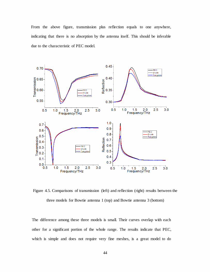
From the above figure, transmission plus reflection equals to one anywhere,
indicating that there is no absorption by the antenna itself. This should be inferable
due to the characteristic of PEC model.
Figure 4.5. Comparisons of transmission (left) and reflection (right) results between the
three models for Bowtie antenna 1 (top) and Bowtie antenna 3 (bottom)
The difference among these three models is small. Their curves overlap with each
other for a significant portion of the whole range. The results indicate that PEC,
which is simple and does not require very fine meshes, is a great model to do

45
simulation. Therefore, in all the simulations, the material of the terahertz antenna is
set to be PEC. Moreover, Tungsten is also a decent choice when the accuracy
requirement is not rigid.
4.2. Comparison of simulation results to existing references
In order to verify that our simulations using Lumerical FDTD solutions are valid,
modeling results are compared to some available data [50]. In this reference, both
simulation and experiment were implemented to study the transmission of spiral-
type terahertz antennas with square windings.
Figure 4.6. Microscopic images of fabricated devices of the spiral type with different
winding numbers (From the reference paper [50])
We model the same structures in Lumerical and compare results with the reference.

46
Figure 4.7. Transmission results of spiral antenna with winding number 3 (the second one
of Figure 4.6) from the reference (left, blue line is for simulation and red line is for
experiment) and from our simulation (right)
Upon comparison, the conclusions are:
a. For the resonant locations, they match well, the two local minimums occur at
about 0.4 and 1.1 THz;
b. For the transmitted values, there is a 0.2 difference for the base lines from
where the curves begin to drop. Our lines start from 0.7 while their lines start from
0.9. Also, the difference of values between the two peaks differs. For the left, it is
0.4-0.2=0.2 while for the right it is 0.4-0=0.4.
Possible causes of these differences may be:
a. Simulation methods are different. They use a method called Fourier-model
method while our simulation bases on FDTD method;
b. Material parameters. For antenna, they use a Drude model for aluminum and
we use Perfect Electrical Conductor (PEC). However, this factor hardly matters. For
47
silicon substrate, their parameters are 0.64-mm-thick, n-type, resistivity 12 Ωcm. In
experiment, they normalize the result with bare silicon. For us, the thickness of
silicon substrate is set to be infinite and the material is not absorbing;
c. Some potential inappropriateness may cause the differences.
The simplest guess of the working frequency of a specific dipole or bowtie antenna
is that the total length of the antenna is equal to the half wavelength (quarter
wavelength is roughly equal to the length of one element of antenna). In this part,
some results from references and from our simulations are shown for us to see
whether this theory is valid for our models.
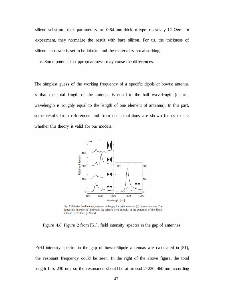
Figure 4.8. Figure 2 from [51], field intensity spectra in the gap of antennas
Field intensity spectra in the gap of bowtie/dipole antennas are calculated in [51],
the resonant frequency could be seen. In the right of the above figure, the total
length L is 230 nm, so the resonance should be at around 2×230=460 nm according
48
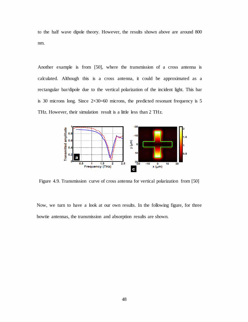
to the half wave dipole theory. However, the results shown above are around 800
nm.
Another example is from [50], where the transmission of a cross antenna is
calculated. Although this is a cross antenna, it could be approximated as a
rectangular bar/dipole due to the vertical polarization of the incident light. This bar
is 30 microns long. Since 2×30=60 microns, the predicted resonant frequency is 5
THz. However, their simulation result is a little less than 2 THz.
Figure 4.9. Transmission curve of cross antenna for vertical polarization from [50]
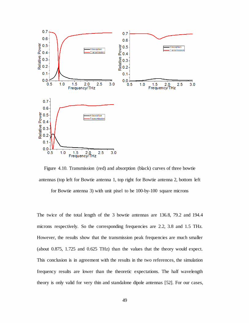
Now, we turn to have a look at our own results. In the following figure, for three
bowtie antennas, the transmission and absorption results are shown.
49
Figure 4.10. Transmission (red) and absorption (black) curves of three bowtie
antennas (top left for Bowtie antenna 1, top right for Bowtie antenna 2, bottom left
for Bowtie antenna 3) with unit pixel to be 100-by-100 square microns
The twice of the total length of the 3 bowtie antennas are 136.8, 79.2 and 194.4
microns respectively. So the corresponding frequencies are 2.2, 3.8 and 1.5 THz.
However, the results show that the transmission peak frequencies are much smaller
(about 0.875, 1.725 and 0.625 THz) than the values that the theory would expect.
This conclusion is in agreement with the results in the two references, the simulation
frequency results are lower than the theoretic expectations. The half wavelength
theory is only valid for very thin and standalone dipole antennas [52]. For our cases,
50
the antenna is sitting on the silicon substrate. We shall expect that the substrate
would affect the frequency response of the antenna as compared to standalone
antennas.
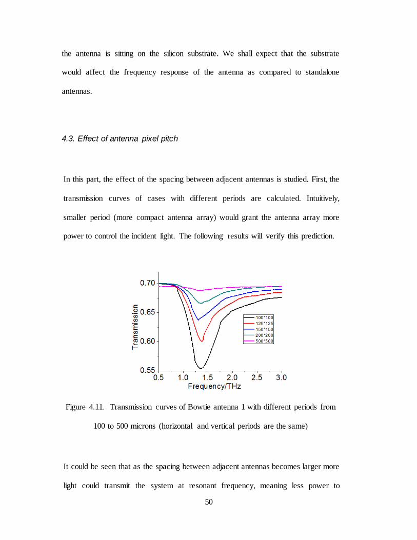
4.3. Effect of antenna pixel pitch
In this part, the effect of the spacing between adjacent antennas is studied. First, the
transmission curves of cases with different periods are calculated. Intuitively,
smaller period (more compact antenna array) would grant the antenna array more
power to control the incident light. The following results will verify this prediction.
Figure 4.11. Transmission curves of Bowtie antenna 1 with different periods from
100 to 500 microns (horizontal and vertical periods are the same)
It could be seen that as the spacing between adjacent antennas becomes larger more
light could transmit the system at resonant frequency, meaning less power to
51
control the incident energy. Therefore, to get higher system efficiency, it is a good
idea to make densely packed antenna arrays.
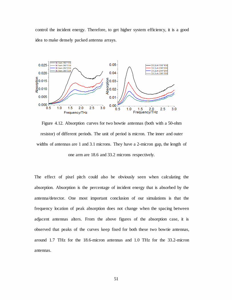
Figure 4.12. Absorption curves for two bowtie antennas (both with a 50-ohm
resistor) of different periods. The unit of period is micron. The inner and outer
widths of antennas are 1 and 3.1 microns. They have a 2-micron gap, the length of
one arm are 18.6 and 33.2 microns respectively.
The effect of pixel pitch could also be obviously seen when calculating the
absorption. Absorption is the percentage of incident energy that is absorbed by the
antenna/detector. One most important conclusion of our simulations is that the
frequency location of peak absorption does not change when the spacing between
adjacent antennas alters. From the above figures of the absorption case, it is
observed that peaks of the curves keep fixed for both these two bowtie antennas,
around 1.7 THz for the 18.6-micron antennas and 1.0 THz for the 33.2-micron
antennas.

52
Numerically, it is noted that the peak values of antenna with a period of 150*150
microns is around four times of the peak values of antenna with a period of 300*300
microns. Since the former case has four times antennas in number as the latter case,
it could be summarized that the absolute absorption for a single antenna is fixed.
Therefore, in order to absorb as more energy as possible, it is desired to have more
antennas in the unit area, which means densely packed array should be considered
favorable.
4.4. Broadband bowtie antenna
Inspired by the report of a French group [53, 54], bowtie antennas with wider taper
could cover a larger range of wavelengths, therefore some tests have been made.
The following pictured are extracted from their report to offer a brief impression of
their design.
Figure 4.13. Sketch of the Bowtie antenna mentioned in the report of the French
group [53]
53
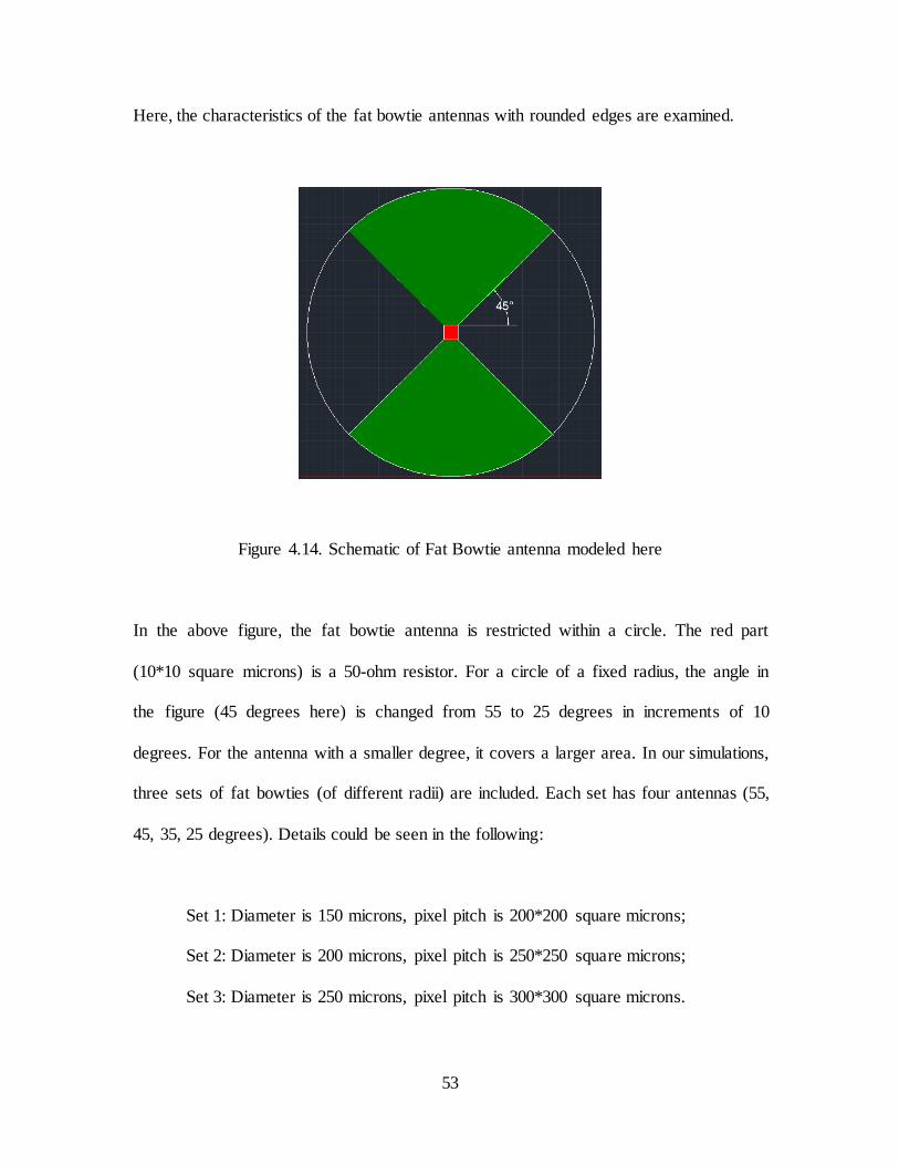
Here, the characteristics of the fat bowtie antennas with rounded edges are examined.
Figure 4.14. Schematic of Fat Bowtie antenna modeled here
In the above figure, the fat bowtie antenna is restricted within a circle. The red part
(10*10 square microns) is a 50-ohm resistor. For a circle of a fixed radius, the angle in
the figure (45 degrees here) is changed from 55 to 25 degrees in increments of 10
degrees. For the antenna with a smaller degree, it covers a larger area. In our simulations,
three sets of fat bowties (of different radii) are included. Each set has four antennas (55,
45, 35, 25 degrees). Details could be seen in the following:
Set 1: Diameter is 150 microns, pixel pitch is 200*200 square microns;
Set 2: Diameter is 200 microns, pixel pitch is 250*250 square microns;
Set 3: Diameter is 250 microns, pixel pitch is 300*300 square microns.
54
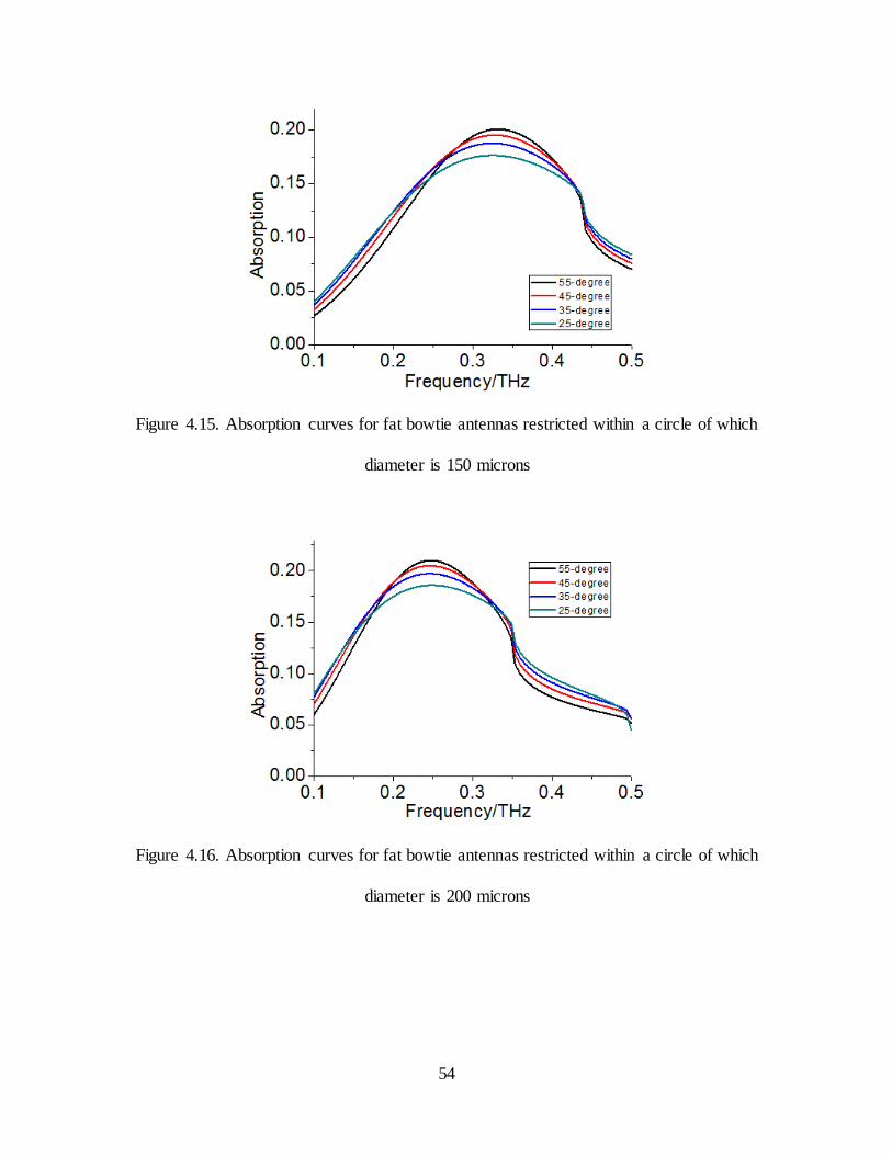
Figure 4.15. Absorption curves for fat bowtie antennas restricted within a circle of which
diameter is 150 microns
Figure 4.16. Absorption curves for fat bowtie antennas restricted within a circle of which
diameter is 200 microns

55
Figure 4.17. Absorption curves for fat bowtie antennas restricted within a circle of which
diameter is 250 microns
From the above three sets of curves, a most significant feature is that for a specific
diameter, the resonant frequency keeps at a fixed location no matter how wide the angle
is. Actually, this is an intuitive conclusion. The longest distance between two points
within the antenna keeps the same for a set of a specific diameter. In the following table,
the values are illustrated.
Antenna Diameter/micron Resonant frequency/THz Resonant wavelength/micron
150 0.33 910
200 0.25 1200
250 0.20 1500
Table 4.1. Resonant frequency/wavelength information for fat bowties of three
different diameters
56
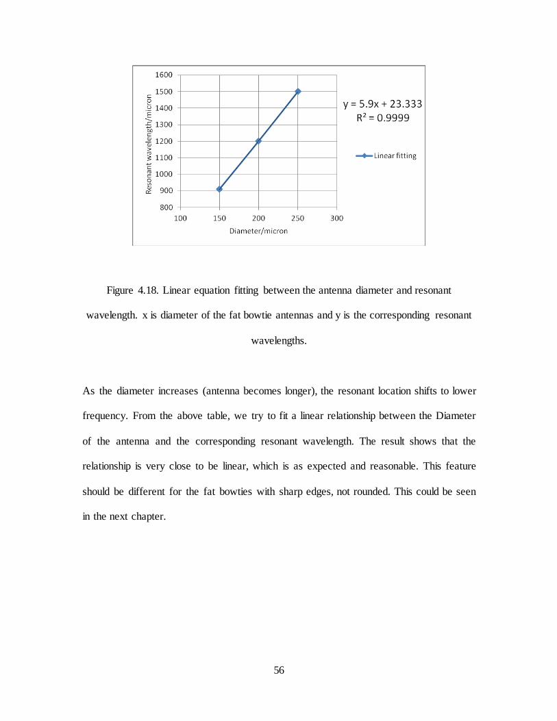
Figure 4.18. Linear equation fitting between the antenna diameter and resonant
wavelength. x is diameter of the fat bowtie antennas and y is the corresponding resonant
wavelengths.
As the diameter increases (antenna becomes longer), the resonant location shifts to lower
frequency. From the above table, we try to fit a linear relationship between the Diameter
of the antenna and the corresponding resonant wavelength. The result shows that the
relationship is very close to be linear, which is as expected and reasonable. This feature
should be different for the fat bowties with sharp edges, not rounded. This could be seen
in the next chapter.

57
Figure 4.19. Pixel photograph of French group design [53]
The validity of this fitting equation could be roughly checked by looking at the design of
French group. In Figure 4.19, the diameter of the fat bowtie antenna (works at 300GHz)
with rounded edges is about 150 microns. The calculated resonant wavelength for
antenna with a 150-micron diameter should be 908 microns from the equation in Figure
4.18. Considering that 300GHz corresponds to 900 microns, this prediction is very
accurate.
Another noticeable feature is that as the angle becomes smaller (the antenna covers a
larger area), the peak value drops down a little. However, the absorption curve becomes
wider, which is reasonable for a fatter antenna.
58
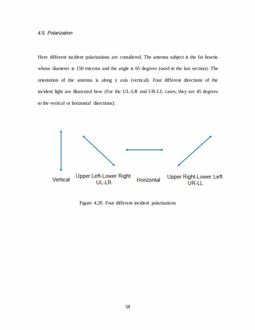
4.5. Polarization
Here different incident polarizations are considered. The antenna subject is the fat bowtie
whose diameter is 150 microns and the angle is 65 degrees (used in the last section). The
orientation of the antenna is along y axis (vertical). Four different directions of the
incident light are illustrated here (For the UL-LR and UR-LL cases, they are 45 degrees
to the vertical or horizontal directions):
Figure 4.20. Four different incident polarizations
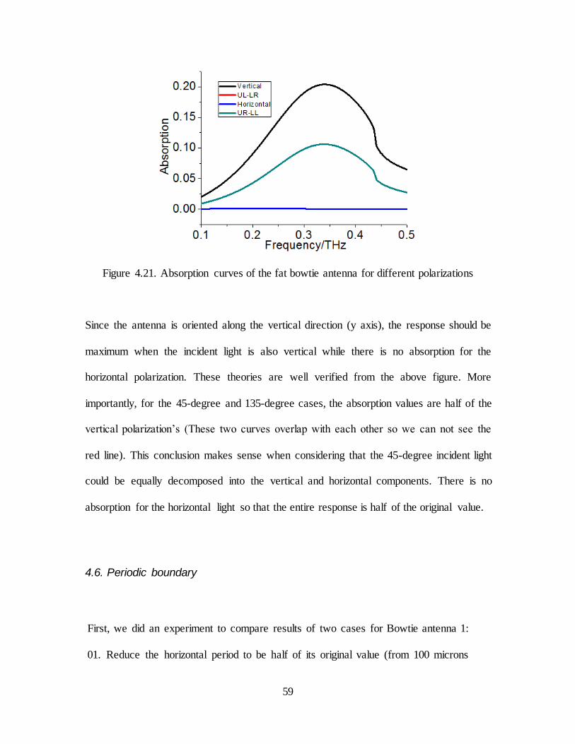
59
Figure 4.21. Absorption curves of the fat bowtie antenna for different polarizations
Since the antenna is oriented along the vertical direction (y axis), the response should be
maximum when the incident light is also vertical while there is no absorption for the
horizontal polarization. These theories are well verified from the above figure. More
importantly, for the 45-degree and 135-degree cases, the absorption values are half of the
vertical polarization’s (These two curves overlap with each other so we can not see the
red line). This conclusion makes sense when considering that the 45-degree incident light
could be equally decomposed into the vertical and horizontal components. There is no
absorption for the horizontal light so that the entire response is half of the original value.
4.6. Periodic boundary
First, we did an experiment to compare results of two cases for Bowtie antenna 1:
01. Reduce the horizontal period to be half of its original value (from 100 microns
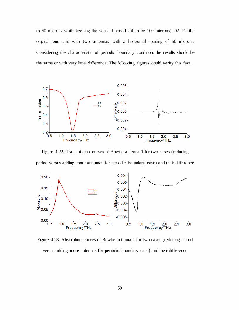
60
to 50 microns while keeping the vertical period still to be 100 microns); 02. Fill the
original one unit with two antennas with a horizontal spacing of 50 microns.
Considering the characteristic of periodic boundary condition, the results should be
the same or with very little difference. The following figures could verify this fact.
Figure 4.22. Transmission curves of Bowtie antenna 1 for two cases (reducing
period versus adding more antennas for periodic boundary case) and their difference
Figure 4.23. Absorption curves of Bowtie antenna 1 for two cases (reducing period
versus adding more antennas for periodic boundary case) and their difference
61
After observing the above two sets of figures, the conclusion is that the curves
almost overlap with each other and the difference is negligible. Reducing the period
is equivalent to the case in which one fills more antennas in one unit (the simulation
area). Therefore, we could simply change the size of the unit area and still only
contain one antenna in the region.
Another similar test is done here. Since the boundary condition around the simulation
area is periodic, modeling of one antenna is equivalent to a 2-D infinite antenna array. In
order to verify this feature, three simulations are implemented: they have 1*1, 2*2, 3*3
antennas/pixels within the boundary respectively. The unit antenna is the same one used
for the above polarization comparison. Theoretically, the responses of these three should
be equal to each other. The modeling result is shown below. The three curves almost
overlap together, indicating that our simulations make sense in terms of the boundary
condition utilized. There is little numerical artifact.

62
Figure 4.24. Absorption results for simulations checking the effect of periodic boundary.
Three simulations have 1*1, 2*2, 3*3 antennas/pixels within the boundary respectively.
4.7. Load resistance
A simple exploration of the effect of resistance on the absorption is implemented here.
The conductivity of the resistor material in the model could be adjusted to control the
resistance. The variation is from 20 to 100 ohms as indicated in the following figure.
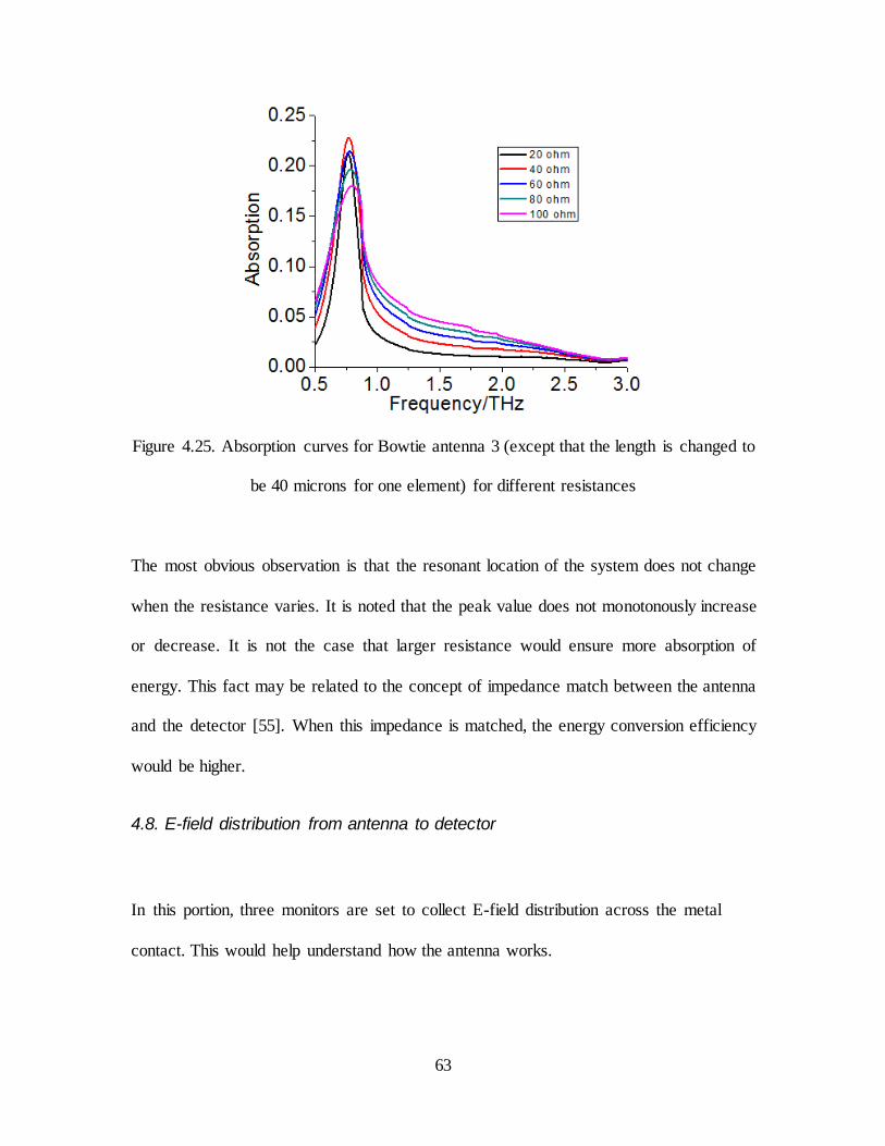
63
Figure 4.25. Absorption curves for Bowtie antenna 3 (except that the length is changed to
be 40 microns for one element) for different resistances
The most obvious observation is that the resonant location of the system does not change
when the resistance varies. It is noted that the peak value does not monotonously increase
or decrease. It is not the case that larger resistance would ensure more absorption of
energy. This fact may be related to the concept of impedance match between the antenna
and the detector [55]. When this impedance is matched, the energy conversion efficiency
would be higher.
4.8. E-field distribution from antenna to detector
In this portion, three monitors are set to collect E-field distribution across the metal
contact. This would help understand how the antenna works.

64
Figure 4.26. Side profile of antenna with the locations of the three monitors
indicated. Three monitors (M1, M2, M3) are put across the metal contact to detect
the E-field distribution information. Not to scale.
Parameters of the bowtie antenna used:
Inner width: 1 micron
Outer width: 3.1 microns
Length of each element: 18.6 microns
Gap: 2 microns
Unit size/period: 40*40 square microns
The 2D E-field distributions (for 1.52THz) are as follows for the three monitors:
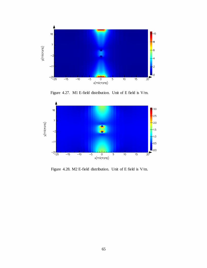
65
Figure 4.27. M1 E-field distribution. Unit of E field is V/m.
Figure 4.28. M2 E-field distribution. Unit of E field is V/m.

66
Figure 4.29. M3 E-field distribution. Unit of E field is V/m.
For M1, which is close to the antenna, E field concentrates at the two ends.
However, as monitor moves downside, the field tends to focus toward the middle
part. This simulation verifies that the antenna qualitatively works as expected. The
antenna of relatively larger shape functions as a collector that draws incident light
that impinging on a large area to the central absorbing element, greatly enhancing
the energy efficiency and detection sensitivity.
4.9. Antenna thickness
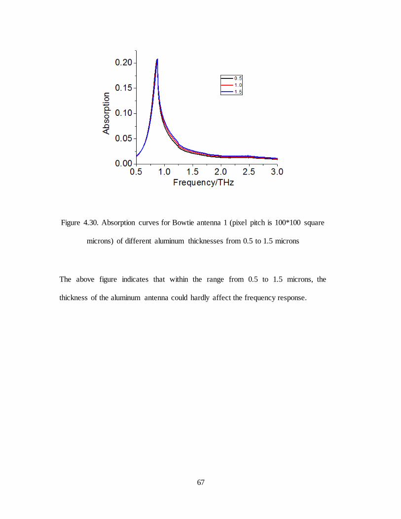
67
Figure 4.30. Absorption curves for Bowtie antenna 1 (pixel pitch is 100*100 square
microns) of different aluminum thicknesses from 0.5 to 1.5 microns
The above figure indicates that within the range from 0.5 to 1.5 microns, the
thickness of the aluminum antenna could hardly affect the frequency response.

68
5. 215GHz & 188GHz Antenna Design
Now that we obtain some knowledge through various tests in the last chapter, we have
the ability to design a specific antenna for certain interested spectral band. In this chapter,
the main focus is to design a broadband terahertz antenna at 215THz. Some practical
issues will be addressed as the designing process goes on. Moreover, one transmission
experiment design utilizing an available 188GHz source will be implemented in order to
verify the validity of the FDTD simulations. Finally, angular frequency response will be
considered for further applications like antenna gain calculation.
5.1. 215 GHz bowtie antenna design
5.1.1. Frequency design
For the three bowtie antennas of the first generation, the resonant frequency information
is listed in the following table.

69
Bowtie 1 Bowtie 2 Bowtie 3
Arm length/micron 33.2 18.8 47.6
Antenna length/micron 68.4 39.6 97.2
Peak absorption frequency/THz 0.875 1.625 0.625
Peak absorption wavelength/micron 343 185 480
Table 5.1. Resonant frequency information for the three bowtie antennas of the first
generation. The first row is length for one arm of the antenna. Since the gap between the
two arms is 2 microns, the antenna length (the second row) is two times the values in the
first row and then plus the gap.
Figure 5.1. Linear equation fitting between the antenna length and resonant wavelength
for first generation bowtie antennas
The linear equation derived from the above data is
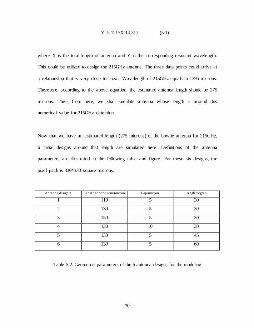
70
Y=5.1215X-14.312 (5.1)
where X is the total length of antenna and Y is the corresponding resonant wavelength.
This could be utilized to design the 215GHz antenna. The three data points could arrive at
a relationship that is very close to linear. Wavelength of 215GHz equals to 1395 microns.
Therefore, according to the above equation, the estimated antenna length should be 275
microns. Then, from here, we shall simulate antenna whose length is around this
numerical value for 215GHz detection.
Now that we have an estimated length (275 microns) of the bowtie antenna for 215GHz,
6 initial designs around that length are simulated here. Definitions of the antenna
parameters are illustrated in the following table and figure. For these six designs, the
pixel pitch is 330*330 square microns.
Antenna design # Length for one arm/micron Gap/micron Angle/degree
1 110 5 30
2 130 5 30
3 150 5 30
4 130 10 30
5 130 5 45
6 130 5 60
Table 5.2. Geometric parameters of the 6 antenna designs for the modeling
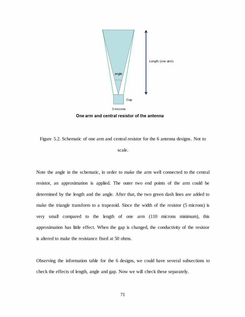
71
Figure 5.2. Schematic of one arm and central resistor for the 6 antenna designs. Not to
scale.
Note the angle in the schematic, in order to make the arm well connected to the central
resistor, an approximation is applied. The outer two end points of the arm could be
determined by the length and the angle. After that, the two green dash lines are added to
make the triangle transform to a trapezoid. Since the width of the resistor (5 microns) is
very small compared to the length of one arm (110 microns minimum), this
approximation has little effect. When the gap is changed, the conductivity of the resistor
is altered to make the resistance fixed at 50 ohms.
Observing the information table for the 6 designs, we could have several subsections to
check the effects of length, angle and gap. Now we will check these separately.

72
For the first subsection, antenna 1, 2, 3 have different lengths.
Figure 5.3. Absorption responses for antennas of different lengths
These three antennas have same angle and gap. A longer antenna should have a larger
resonant wavelength, which corresponds to a smaller frequency. Therefore, from the 110
to 150 microns, the location of peak absorption shifts to left. This is an obvious feather in
the above figure. The resonant frequencies are 215GHz, 185GHz and 156GHz. Also, a
longer antenna would cover a larger area, making the longer antenna has a slightly
uprising curve, absorbing a larger portion of the incident radiation.
In the second subsection, antenna 2, 5, 6 have the same length, gap and different angles.

73
Figure 5.4. Absorption responses for antennas of different angles
In this case, antennas have the same length. However, a larger angle makes the antenna
behaves as if it is a little longer than the thinner ones. So the 60-degree antenna has the
smallest resonant frequency. The difference between these three curves is smaller
compared to the length effect shown in the last part.
Now, we turn to briefly look at the effect of gap. Between antenna 2 and 4, the only
difference is the gap seen from Table 5.2. However, since the total length of the antenna
equals to two times the arm length and plus the gap. The difference between two curves
of the following figure is not negligible, but this may not be the cause of the gap.
Analysis for the effect of the gap could be seen later in the thesis.
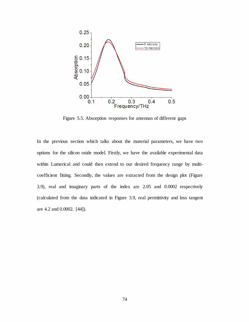
74
Figure 5.5. Absorption responses for antennas of different gaps
In the previous section which talks about the material parameters, we have two
options for the silicon oxide model. Firstly, we have the available experimental data
within Lumerical and could then extend to our desired frequency range by multi-
coefficient fitting. Secondly, the values are extracted from the design plot (Figure
3.9), real and imaginary parts of the index are 2.05 and 0.0002 respectively
(calculated from the data indicated in Figure 3.9, real permittivity and loss tangent
are 4.2 and 0.0002. [44]).
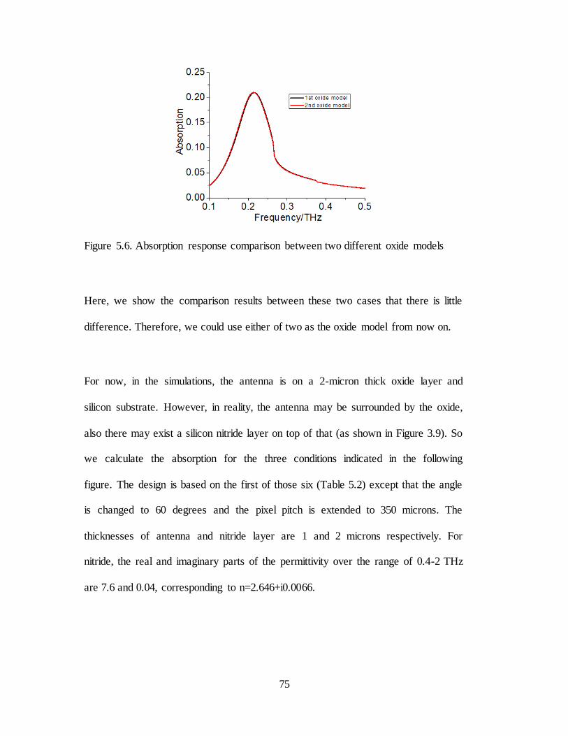
75
Figure 5.6. Absorption response comparison between two different oxide models
Here, we show the comparison results between these two cases that there is little
difference. Therefore, we could use either of two as the oxide model from now on.
For now, in the simulations, the antenna is on a 2-micron thick oxide layer and
silicon substrate. However, in reality, the antenna may be surrounded by the oxide,
also there may exist a silicon nitride layer on top of that (as shown in Figure 3.9). So
we calculate the absorption for the three conditions indicated in the following
figure. The design is based on the first of those six (Table 5.2) except that the angle
is changed to 60 degrees and the pixel pitch is extended to 350 microns. The
thicknesses of antenna and nitride layer are 1 and 2 microns respectively. For
nitride, the real and imaginary parts of the permittivity over the range of 0.4-2 THz
are 7.6 and 0.04, corresponding to n=2.646+i0.0066.
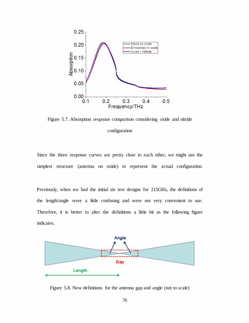
76
Figure 5.7. Absorption response comparison considering oxide and nitride
configuration
Since the three response curves are pretty close to each other, we might use the
simplest structure (antenna on oxide) to represent the actual configuration.
Previously, when we had the initial six test designs for 215GHz, the definitions of
the length/angle were a little confusing and were not very convenient to use.
Therefore, it is better to alter the definitions a little bit as the following figure
indicates.
Figure 5.8. New definitions for the antenna gap and angle (not to scale)
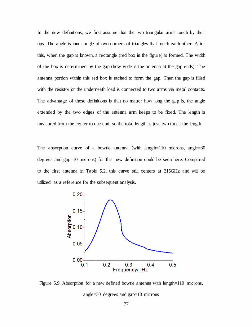
77
In the new definitions, we first assume that the two triangular arms touch by their
tips. The angle is inner angle of two corners of triangles that touch each other. After
this, when the gap is known, a rectangle (red box in the figure) is formed. The width
of the box is determined by the gap (how wide is the antenna at the gap ends). The
antenna portion within this red box is etched to form the gap. Then the gap is filled
with the resistor or the underneath load is connected to two arms via metal contacts.
The advantage of these definitions is that no matter how long the gap is, the angle
extended by the two edges of the antenna arm keeps to be fixed. The length is
measured from the center to one end, so the total length is just two times the length.
The absorption curve of a bowtie antenna (with length=110 microns, angle=30
degrees and gap=10 microns) for this new definition could be seen here. Compared
to the first antenna in Table 5.2, this curve still centers at 215GHz and will be
utilized as a reference for the subsequent analysis.
Figure 5.9. Absorption for a new defined bowtie antenna with length=110 microns,
angle=30 degrees and gap=10 microns
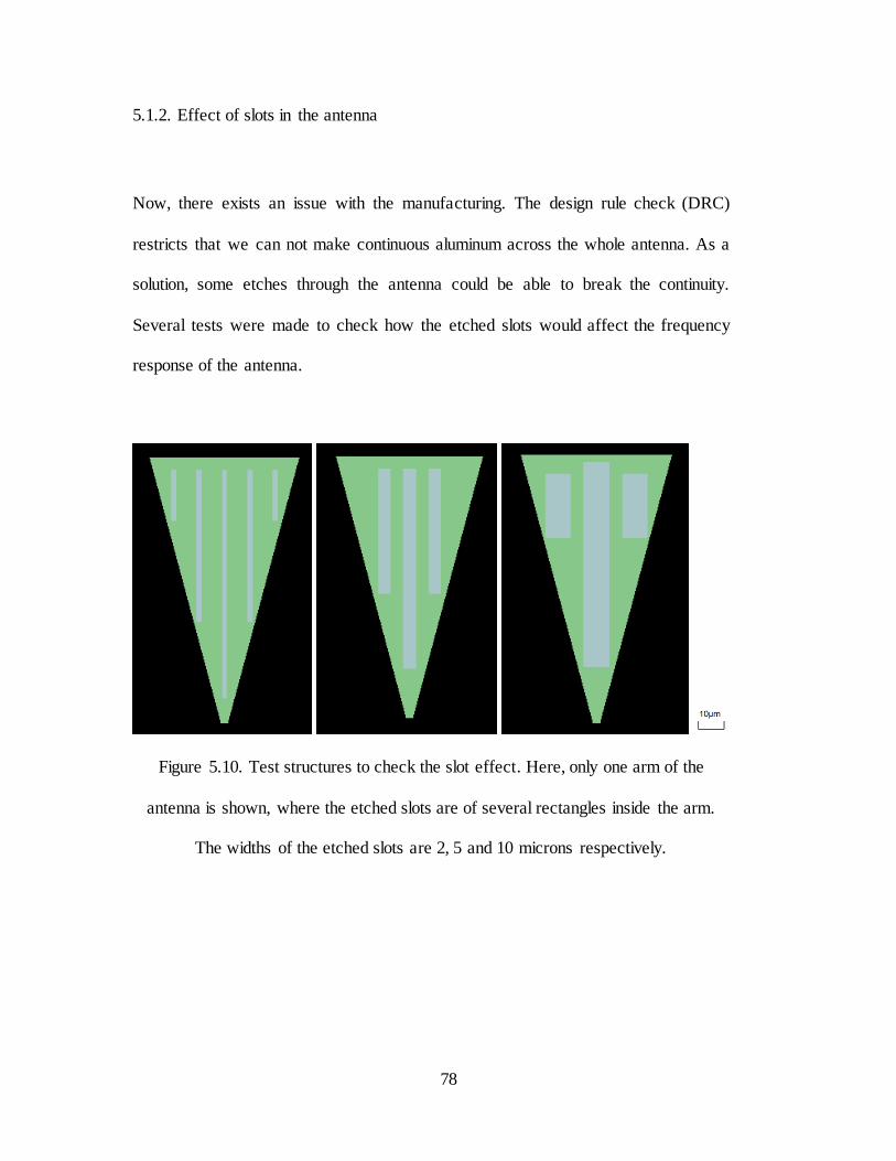
78
5.1.2. Effect of slots in the antenna
Now, there exists an issue with the manufacturing. The design rule check (DRC)
restricts that we can not make continuous aluminum across the whole antenna. As a
solution, some etches through the antenna could be able to break the continuity.
Several tests were made to check how the etched slots would affect the frequency
response of the antenna.
Figure 5.10. Test structures to check the slot effect. Here, only one arm of the
antenna is shown, where the etched slots are of several rectangles inside the arm.
The widths of the etched slots are 2, 5 and 10 microns respectively.
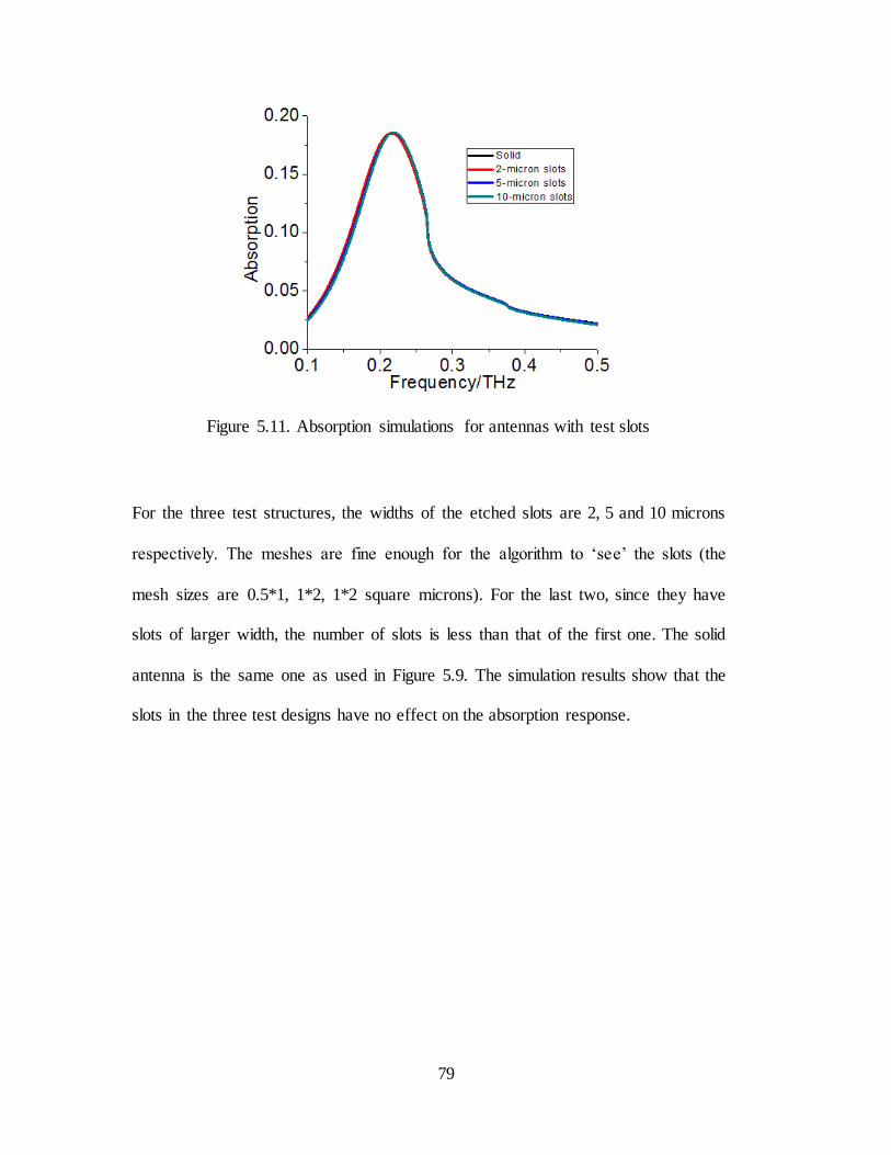
79
Figure 5.11. Absorption simulations for antennas with test slots
For the three test structures, the widths of the etched slots are 2, 5 and 10 microns
respectively. The meshes are fine enough for the algorithm to ‘see’ the slots (the
mesh sizes are 0.5*1, 1*2, 1*2 square microns). For the last two, since they have
slots of larger width, the number of slots is less than that of the first one. The solid
antenna is the same one as used in Figure 5.9. The simulation results show that the
slots in the three test designs have no effect on the absorption response.

80
Figure 5.12. Two tests for antennas with etched blocks. The sizes of the blocks are
5*5, 30*40 square microns respectively.
Two more tests were made. For the first, there were nine small etched blocks in
each arm. For the second, there was one large etched block in each arm. The sizes of
the blocks were 5*5, 30*40 square microns respectively. From the above figure
showing the comparison between the solid antenna and the antenna with etched
blocks, the antenna with small blocks has the same response with the solid one.
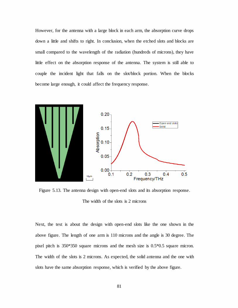
81
However, for the antenna with a large block in each arm, the absorption curve drops
down a little and shifts to right. In conclusion, when the etched slots and blocks are
small compared to the wavelength of the radiation (hundreds of microns), they have
little effect on the absorption response of the antenna. The system is still able to
couple the incident light that falls on the slot/block portion. When the blocks
become large enough, it could affect the frequency response.
Figure 5.13. The antenna design with open-end slots and its absorption response.
The width of the slots is 2 microns
Next, the test is about the design with open-end slots like the one shown in the
above figure. The length of one arm is 110 microns and the angle is 30 degree. The
pixel pitch is 350*350 square microns and the mesh size is 0.5*0.5 square micron.
The width of the slots is 2 microns. As expected, the solid antenna and the one with
slots have the same absorption response, which is verified by the above figure.
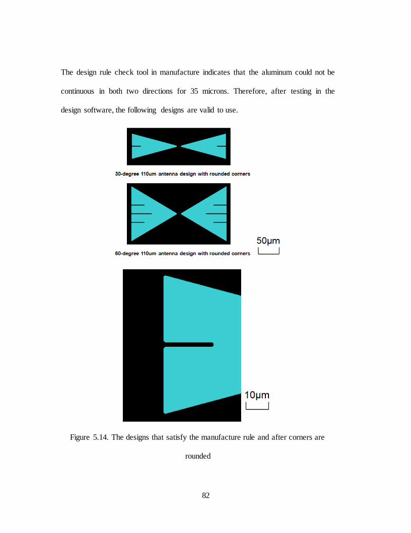
82
The design rule check tool in manufacture indicates that the aluminum could not be
continuous in both two directions for 35 microns. Therefore, after testing in the
design software, the following designs are valid to use.
Figure 5.14. The designs that satisfy the manufacture rule and after corners are
rounded
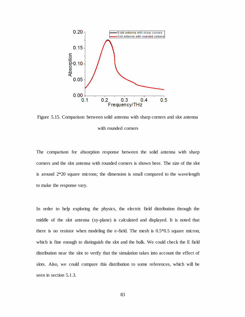
83
Figure 5.15. Comparison between solid antenna with sharp corners and slot antenna
with rounded corners
The comparison for absorption response between the solid antenna with sharp
corners and the slot antenna with rounded corners is shown here. The size of the slot
is around 2*20 square microns; the dimension is small compared to the wavelength
to make the response vary.
In order to help exploring the physics, the electric field distribution through the
middle of the slot antenna (xy-plane) is calculated and displayed. It is noted that
there is no resistor when modeling the e-field. The mesh is 0.5*0.5 square micron,
which is fine enough to distinguish the slot and the bulk. We could check the E field
distribution near the slot to verify that the simulation takes into account the effect of
slots. Also, we could compare this distribution to some references, which will be
seen in section 5.1.3.
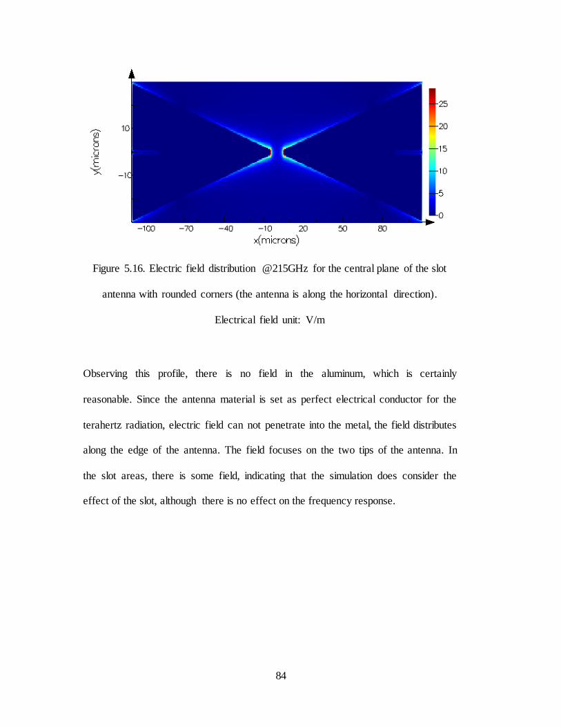
84
Figure 5.16. Electric field distribution @215GHz for the central plane of the slot
antenna with rounded corners (the antenna is along the horizontal direction).
Electrical field unit: V/m
Observing this profile, there is no field in the aluminum, which is certainly
reasonable. Since the antenna material is set as perfect electrical conductor for the
terahertz radiation, electric field can not penetrate into the metal, the field distributes
along the edge of the antenna. The field focuses on the two tips of the antenna. In
the slot areas, there is some field, indicating that the simulation does consider the
effect of the slot, although there is no effect on the frequency response.
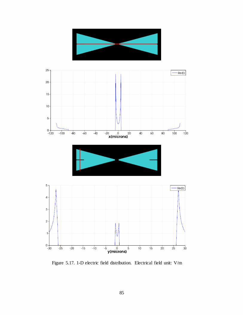
85
Figure 5.17. 1-D electric field distribution. Electrical field unit: V/m

86
The 1-D field patterns could well show the characteristics of the electric field
distribution. For the first case of the above figure, the red line is in the center of the
antenna and along x axis. The values are extremely high in the central tips of the
antenna and quickly drop down away from the edges. For the second red line, since
the width of the open-end slot is very small, the field value in the center of the slot
is not but close to zero.
5.1.3. Effect of antenna gap
If we decrease the gap and increase the inner width of the two arms, theoretically,
we would see a much more uniform field across the gap. The following figures
show a test that has a gap of 5 microns and inner width from 5 to 40 microns. The
mesh size is 1*1 square micron.
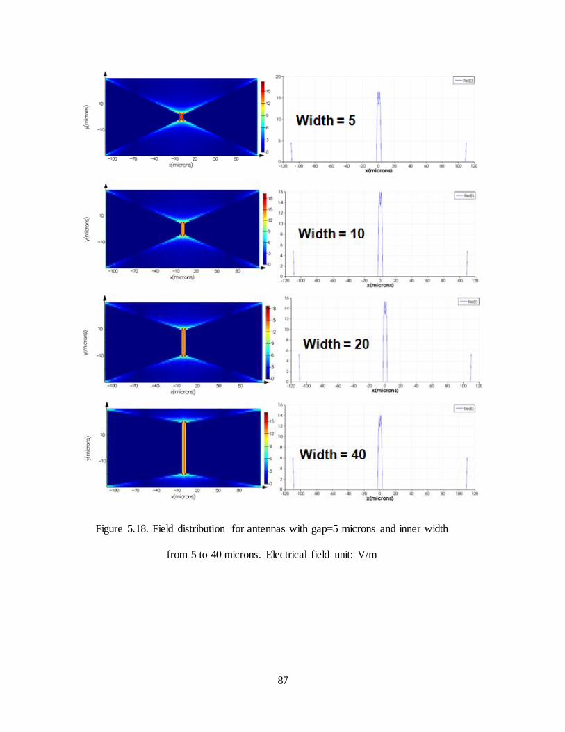
87
Figure 5.18. Field distribution for antennas with gap=5 microns and inner width
from 5 to 40 microns. Electrical field unit: V/m
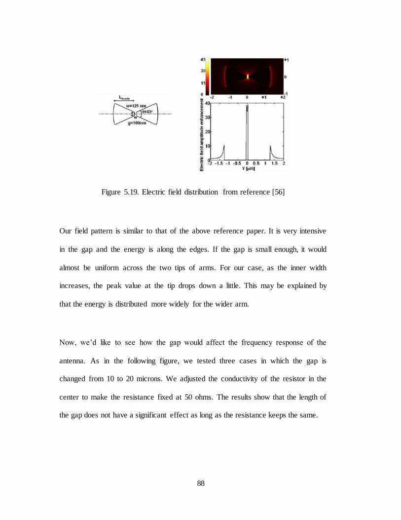
88
Figure 5.19. Electric field distribution from reference [56]
Our field pattern is similar to that of the above reference paper. It is very intensive
in the gap and the energy is along the edges. If the gap is small enough, it would
almost be uniform across the two tips of arms. For our case, as the inner width
increases, the peak value at the tip drops down a little. This may be explained by
that the energy is distributed more widely for the wider arm.
Now, we’d like to see how the gap would affect the frequency response of the
antenna. As in the following figure, we tested three cases in which the gap is
changed from 10 to 20 microns. We adjusted the conductivity of the resistor in the
center to make the resistance fixed at 50 ohms. The results show that the length of
the gap does not have a significant effect as long as the resistance keeps the same.

89
Figure 5.20. Absorption responses when the gap is changed from 10 to 20 microns
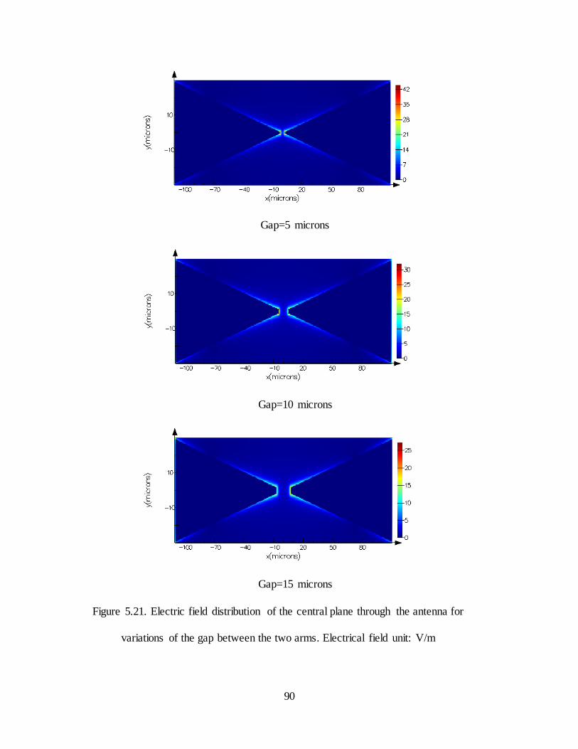
90
Gap=5 microns
Gap=10 microns
Gap=15 microns
Figure 5.21. Electric field distribution of the central plane through the antenna for
variations of the gap between the two arms. Electrical field unit: V/m
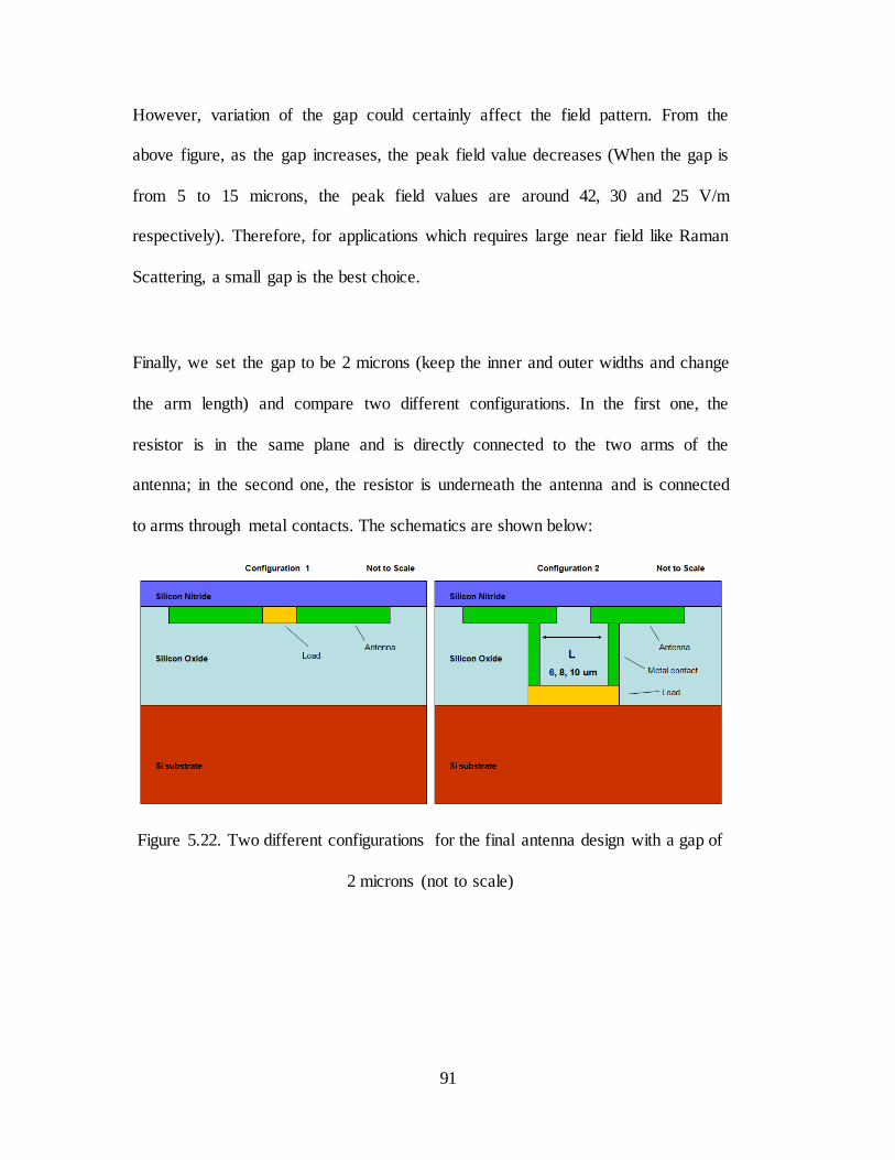
91
However, variation of the gap could certainly affect the field pattern. From the
above figure, as the gap increases, the peak field value decreases (When the gap is
from 5 to 15 microns, the peak field values are around 42, 30 and 25 V/m
respectively). Therefore, for applications which requires large near field like Raman
Scattering, a small gap is the best choice.
Finally, we set the gap to be 2 microns (keep the inner and outer widths and change
the arm length) and compare two different configurations. In the first one, the
resistor is in the same plane and is directly connected to the two arms of the
antenna; in the second one, the resistor is underneath the antenna and is connected
to arms through metal contacts. The schematics are shown below:
Figure 5.22. Two different configurations for the final antenna design with a gap of
2 microns (not to scale)
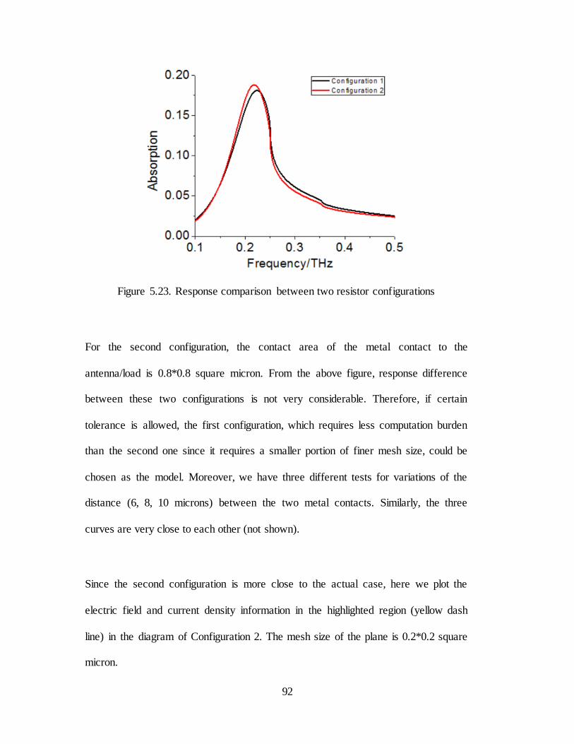
92
Figure 5.23. Response comparison between two resistor configurations
For the second configuration, the contact area of the metal contact to the
antenna/load is 0.8*0.8 square micron. From the above figure, response difference
between these two configurations is not very considerable. Therefore, if certain
tolerance is allowed, the first configuration, which requires less computation burden
than the second one since it requires a smaller portion of finer mesh size, could be
chosen as the model. Moreover, we have three different tests for variations of the
distance (6, 8, 10 microns) between the two metal contacts. Similarly, the three
curves are very close to each other (not shown).
Since the second configuration is more close to the actual case, here we plot the
electric field and current density information in the highlighted region (yellow dash
line) in the diagram of Configuration 2. The mesh size of the plane is 0.2*0.2 square
micron.
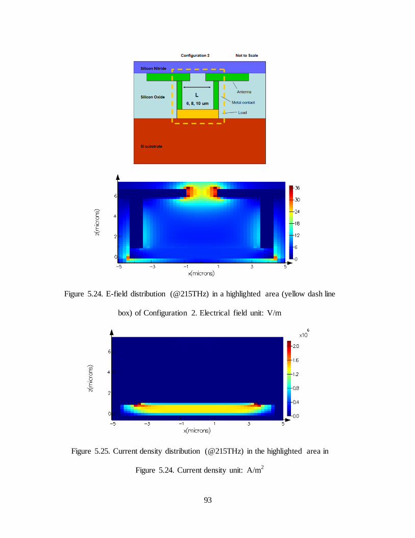
93
Figure 5.24. E-field distribution (@215THz) in a highlighted area (yellow dash line
box) of Configuration 2. Electrical field unit: V/m
Figure 5.25. Current density distribution (@215THz) in the highlighted area in
Figure 5.24. Current density unit: A/m2
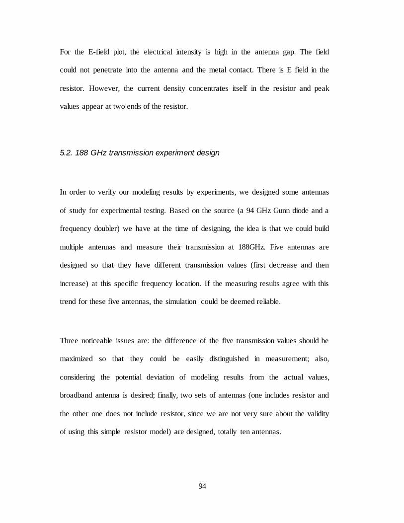
94
For the E-field plot, the electrical intensity is high in the antenna gap. The field
could not penetrate into the antenna and the metal contact. There is E field in the
resistor. However, the current density concentrates itself in the resistor and peak
values appear at two ends of the resistor.
5.2. 188 GHz transmission experiment design
In order to verify our modeling results by experiments, we designed some antennas
of study for experimental testing. Based on the source (a 94 GHz Gunn diode and a
frequency doubler) we have at the time of designing, the idea is that we could build
multiple antennas and measure their transmission at 188GHz. Five antennas are
designed so that they have different transmission values (first decrease and then
increase) at this specific frequency location. If the measuring results agree with this
trend for these five antennas, the simulation could be deemed reliable.
Three noticeable issues are: the difference of the five transmission values should be
maximized so that they could be easily distinguished in measurement; also,
considering the potential deviation of modeling results from the actual values,
broadband antenna is desired; finally, two sets of antennas (one includes resistor and
the other one does not include resistor, since we are not very sure about the validity
of using this simple resistor model) are designed, totally ten antennas.
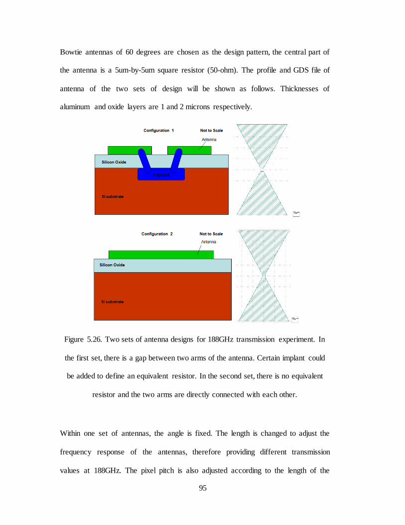
95
Bowtie antennas of 60 degrees are chosen as the design pattern, the central part of
the antenna is a 5um-by-5um square resistor (50-ohm). The profile and GDS file of
antenna of the two sets of design will be shown as follows. Thicknesses of
aluminum and oxide layers are 1 and 2 microns respectively.
Figure 5.26. Two sets of antenna designs for 188GHz transmission experiment. In
the first set, there is a gap between two arms of the antenna. Certain implant could
be added to define an equivalent resistor. In the second set, there is no equivalent
resistor and the two arms are directly connected with each other.
Within one set of antennas, the angle is fixed. The length is changed to adjust the
frequency response of the antennas, therefore providing different transmission
values at 188GHz. The pixel pitch is also adjusted according to the length of the

96
antenna. After many tests, five antennas of different length for each set are chosen
to be manufactured. The corresponding transmission curves are shown here:
Figure 5.27. Transmission curves for two sets of antennas (left, the green line
represents location of 188GHz) and the transmission values at 188GHz (right)
The antenna parameters are listed in the following table:
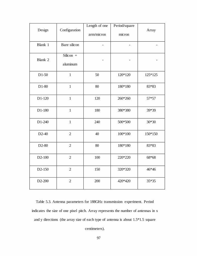
97
Design Configuration Length of one
arm/micron
Period/square
micron Array
Blank 1 Bare silicon - - -
Blank 2 Silicon +
aluminum - - -
D1-50 1 50 120*120 125*125
D1-80 1 80 180*180 83*83
D1-120 1 120 260*260 57*57
D1-180 1 180 380*380 39*39
D1-240 1 240 500*500 30*30
D2-40 2 40 100*100 150*150
D2-80 2 80 180*180 83*83
D2-100 2 100 220*220 68*68
D2-150 2 150 320*320 46*46
D2-200 2 200 420*420 35*35
Table 5.3. Antenna parameters for 188GHz transmission experiment. Period
indicates the size of one pixel pitch. Array represents the number of antennas in x
and y directions (the array size of each type of antenna is about 1.5*1.5 square
centimeters).

98
This experiment is still in progress and the experimental data should be compared to
the right two plots of Figure 5.27.
5.3. Angular response of antenna
One important issue we are interested in is that how the antenna response would be
as the incident angle of incoming radiation changes. Previous modeling assumed all
the incident radiation is normal to the plane where the antenna resides in. We could
compare the angular response of the antenna to the already known antenna radiation
pattern due to the reciprocity theorem (antenna works equally well as transmitters or
receivers) [57].
To ensure the simulation is valid, we first need to verify two simple cases: angular
transmission/reflection of air/silicon interface; angular absorption response of a
dipole antenna of which the radiation pattern is known. After these two, the
combination of them, antenna sitting on silicon substrate, could be implemented.
The transmission and reflection of air/silicon surface for different incident angles
could be calculated from Fresnel equations [58] and simulated from FDTD
Solutions (for component parallel to the incident plane):
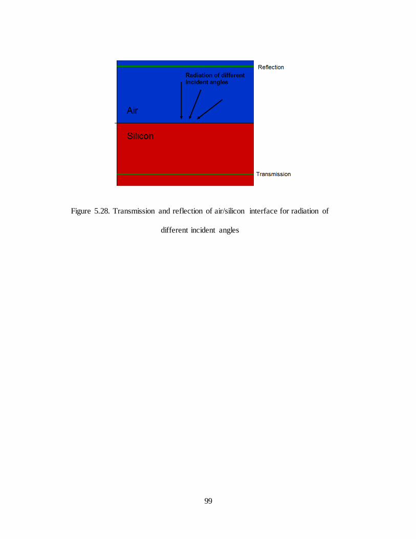
99
Figure 5.28. Transmission and reflection of air/silicon interface for radiation of
different incident angles

100
Figure 5.29. Comparison between theoretic and simulation results for transmission
and reflection of air/silicon interface as a function of incident angle. Blue curves are
of theory and red stars are of simulation results. Source frequency is 0.18THz. For
data points of angle up to 60 degrees, the number of PML layers is 48; for all other
cases with angle larger than 60 degrees, the number of PML layers is set to be 96.
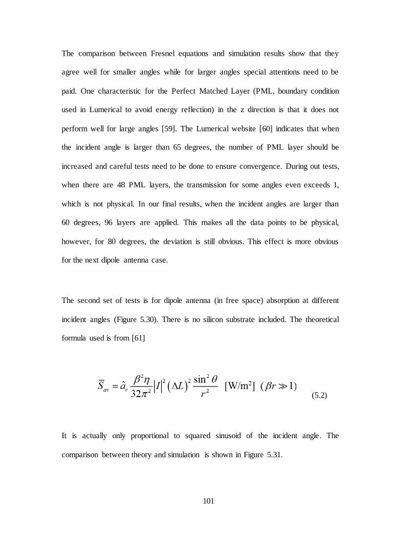
101
The comparison between Fresnel equations and simulation results show that they
agree well for smaller angles while for larger angles special attentions need to be
paid. One characteristic for the Perfect Matched Layer (PML, boundary condition
used in Lumerical to avoid energy reflection) in the z direction is that it does not
perform well for large angles [59]. The Lumerical website [60] indicates that when
the incident angle is larger than 65 degrees, the number of PML layer should be
increased and careful tests need to be done to ensure convergence. During out tests,
when there are 48 PML layers, the transmission for some angles even exceeds 1,
which is not physical. In our final results, when the incident angles are larger than
60 degrees, 96 layers are applied. This makes all the data points to be physical,
however, for 80 degrees, the deviation is still obvious. This effect is more obvious
for the next dipole antenna case.
The second set of tests is for dipole antenna (in free space) absorption at different
incident angles (Figure 5.30). There is no silicon substrate included. The theoretical
formula used is from [61]
(5.2)
It is actually only proportional to squared sinusoid of the incident angle. The
comparison between theory and simulation is shown in Figure 5.31.
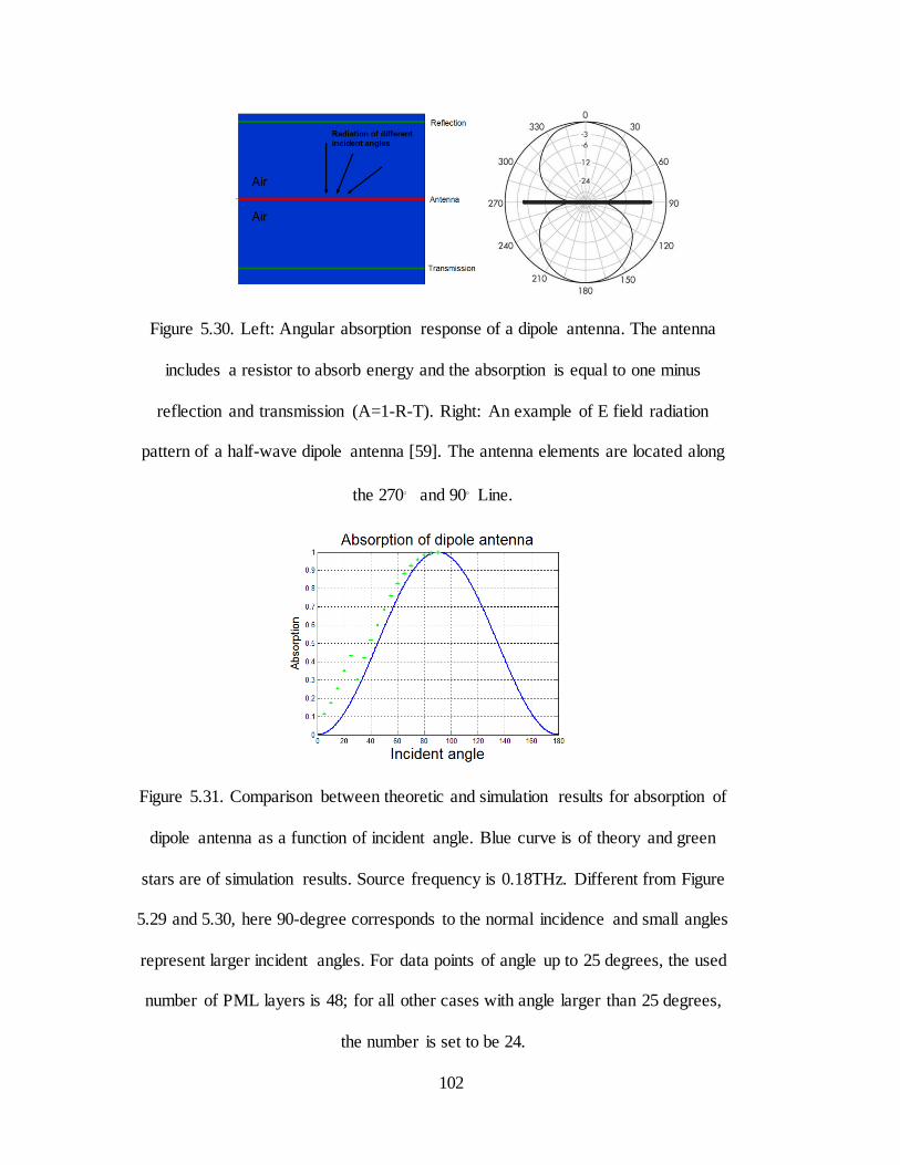
102
Figure 5.30. Left: Angular absorption response of a dipole antenna. The antenna
includes a resistor to absorb energy and the absorption is equal to one minus
reflection and transmission (A=1-R-T). Right: An example of E field radiation
pattern of a half-wave dipole antenna [59]. The antenna elements are located along
the 270。 and 90。Line.
Figure 5.31. Comparison between theoretic and simulation results for absorption of
dipole antenna as a function of incident angle. Blue curve is of theory and green
stars are of simulation results. Source frequency is 0.18THz. Different from Figure
5.29 and 5.30, here 90-degree corresponds to the normal incidence and small angles
represent larger incident angles. For data points of angle up to 25 degrees, the used
number of PML layers is 48; for all other cases with angle larger than 25 degrees,
the number is set to be 24.
103
It should be indicated that the dipole antenna utilized here is 245 microns long, 24
microns wide and thick, which makes the aspect ratio to be about 10. We have tried
the case where width and thickness were both 5 microns and the length was 245
microns. The comparison shows that simulation results for the wider dipole (24
microns) are more close to the theoretical curve. The aspect ratio may be a factor
affecting how close the simulations and theories would be.
To get more accurate simulations, three improvements were implemented: firstly,
for larger incident angles, there were 48 PML layers; secondly, finer mesh size of
1*1 square micron was used; thirdly, the relative location of the reflection monitor
and the source was adjusted, making that the monitor was between the source and
the dipole subject. The fact that the algorithm does not perform well at larger
incident angles is clearer for our dipole antenna angular absorption modeling than
the previous transmission/reflection simulation at air/silicon interface. The number
of PML layers may be increased even larger to reduce the error.
Since these two sets of tests got decent results below an incident angle of around 60
degrees (theoretical and simulation data roughly agree except for some data points
at large incident angles), we could proceed to have a look at the angular response of
our designed bowtie antenna. Some initial simulation results are not very intuitive
so that additional effort needs to be made in the future.
104
5.4. Conclusion and future work
The focus of this thesis is to simulate THz antennas, using the commercial FDTD
software, Lumerical FDTD solutions. For absorption simulation, a mathematically
equivalent resistor is included in the model to transfer THz light into electrical
power. Using PEC as the aluminum antenna material model is fast and the results
are close to the cases using aluminum Drude model. Through many tests, we get
knowledge of how various parameters in the design would affect the performance of
the antenna. The desired antenna design in order to couple incident radiation should
be compact. Most of our simulation results are physical or could be directly
compared to some existing references. There is a linear relationship between the
bowtie antenna length and resonant wavelength, which could help design certain
types of antenna for specific interested spectral bands. Some issues during the
manufacture, like the slots to qualify for the design rule for discontinuity, were
addressed. Some other information, such as E-field distribution, current density,
were also provided for enhancing the understanding. The absorption antenna for
215GHz and transmission experiment at 188GHz were designed and could serve to
verify the validity of the simulation.
In the future, research on some specific deficiencies should be taken into account.
The index of refraction data for materials within terahertz range are not available
and need to be measured. After the 188GHz transmission experiment and 215GHz

105
antenna designs help further verifying the validity of our simulation model, this
model needs to get more complicated to be more close to the actual structure.

106
References
[1] https://nelson.mit.edu/blog/terahertz-polaritonics
[2]
http://www.toptica.com/products/terahertz_generation/terahertz_technologysources_and_
thz_generation_methods/properties_of_terahertz_radiation.html
[3] Gharavi, Sam; Heydari, Babak (2011-09-25). Ultra High-Speed CMOS Circuits :
Beyond 100 GHz (1st ed.). New York: Springer Science+Business Media. pp. 1–5
(Introduction) and 100.
[4] Sirtori, Carlo (2002). "Applied physics: Bridge for the terahertz
gap" . Nature 417 (6885): 132-3
[5] Borak, A. (2005). "Applied physics: Toward Bridging the Terahertz Gap with Silicon-
Based Lasers" Science 308 (5722): 638–9.
[6] Karpowicz, Nicholas; Dai, Jianming; Lu, Xiaofei; Chen, Yunqing; Yamaguchi,
Masashi; Zhao, Hongwei; Zhang, X.-C.; Zhang, Liangliang; Zhang, Cunlin; Price-
Gallagher, Matthew; Fletcher, Clark; Mamer, Orval; Lesimple, Alain; Johnson, Keith
(2008). "Coherent heterodyne time-domain spectrometry covering the entire "terahertz
gap"". Applied Physics Letters (Abstract) 92: 011131
[7] Kleiner, R. (2007). "Filling the Terahertz Gap". Science (Abstract) 318 (5854): 1254–
5
[8] Arnone, Don, Craig Ciesla, and Michael Pepper. "Terahertz imaging comes into
view." Physics World 4 (2000): 35-40.
[9] http://www.dlr.de/pf/desktopdefault.aspx/tabid-833/1333_read-2400/
107
[10] JLab generates high-power terahertz
light http://cerncourier.com/cws/article/cern/28777
[11] Standoff identification of concealed explosives under real-world conditions
[12] Zhao, Jiayu, et al. "Terahertz imaging with sub-wavelength resolution by
femtosecond laser filament in air." Scientific reports 4 (2014).
[13] http://www.digitalbarriers.com/products/thruvision/thruvision-ts5/
[14] Sengupta, Kaushik, and Ali Hajimiri. "A 0.28 THz power-generation and beam-
steering array in CMOS based on distributed active radiators." Solid-State Circuits, IEEE
Journal of 47.12 (2012): 3013-3031.
[15] http://www.z-
thz.com/index.php?option=com_content&view=article&id=51&Itemid=59
[16] http://www.teraview.com/applications/medical/oncology.html
[17] Nagatsuma, Tadao, et al. "Terahertz wireless communications based on photonics
technologies." Optics express 21.20 (2013): 23736-23747.
[18] Akyildiz, Ian F., Josep Miquel Jornet, and Chong Han. "Terahertz band: Next
frontier for wireless communications." Physical Communication 12 (2014): 16-32.
[19] Jördens, Christian, Frank Rutz, and Martin Koch. "Quality assurance of chocolate
products with terahertz imaging." European Conference on NDT. 2006.
[20] Rogalski, A., and F. Sizov. "Terahertz detectors and focal plane arrays." Opto-
electronics review 19.3 (2011): 346-404.
[21] A.D. Turner, J.J. Bock, J.W. Beeman, J. Glenn, P.C. Hargrave, V.V. Hristov, H.T.
Nguyen, F. Rahman, S.Sethuraman, and A.L. Woodcraft, “Silicon nitride micro−mesh
bolometer array for submillimeter astrophysics”, Appl.Optics 40, 4921–4932 (2001).
108
[22] “Detectors needs for long wavelength astrophysics”, A Report by the Infrared,
Submillimeter, and Millimeter Detector Working Group, June 2002;
http://safir.gsfc.nasa.gov/docs/ISMDWG_final.pdf
[23] J. Glenn, P.A.R. Ade, M. Amarie, J.J. Bock, S.F. Edgington, A. Goldin, S. Golwala,
D. Haig, A.E. Lange, G. Laurent, P.D. Maudkopf, M. Yun, and H. Nguyen, “Current
status of Bolocam: a large−format millimeter−wave bolometer camera”, Proc. SPIE
4855, 30–40 (2003).
[24] G.M. Voellmer, C.A. Allen, M.J. Amato, S.R. Babu, A.E.Bartels, D.J. Benford, R.J.
Derro, C.D. Dowell, D.A. Harper, M.D. Jhabvala, S.H. Moseley, T. Rennick, P.J.
Shirron, W.W. Smith, and J.G. Staguhn, “Design and fabrication of two−dimensional
semiconducting bolometer arrays for HAWC and SHARC−II”, Proc. SPIE 4855, 63–72
(2003).
[25] J.G. Staguhn, D.J. Benford, F. Pajot, T.J. Ames, J.A.Chervenak, E.N. Grossman,
K.D. Irwin, B. Maffei, S.H.Moseley, T.G. Phillips, C.D. Reintsema, C. Rioux, R.A.
Shafer, and G.M. Vollmer, “Astronomical demonstration of superconducting bolometer
arrays”, Proc. SPIE 4855,100–107 (2003).
[26] C.M. Bradford, B.J. Naylor, J. Zmuidzinas, J.J. Bock, J.Gromke, H. Nguyen, M.
Dragovan, M. Yun, L. Earle, J.Glenn, H. Matsuhara, P.A.R. Ade, and L. Duband,
“WaFIRS: A waveguide far−IR spectrometer: Enabling spectroscopy of high−z galaxies
in the far−IR and submillimeter”,Proc. SPIE 4850, 1137–1148 (2003)
[27] Webster, John G (1999). The measurement, instrumentation, and sensors handbook.
pp. 32–113.
[28] http://en.wikipedia.org/wiki/Julius_Edgar_Lilienfeld
109
[29] http://www.elprocus.com/mosfet-as-a-switch-circuit-diagram-free-circuits/
[30] Dyakonov, Michael, and Michael Shur. "Shallow water analogy for a ballistic field
effect transistor: New mechanism of plasma wave generation by dc current." Physical
review letters 71.15 (1993): 2465.
[31] Evaluation of MOSFETs for Terahertz Detector Arrays. Gregory Fertig. Master
Thesis, Rochester Institute of Technology, 2014
[32] Knap, W., et al. "Nonresonant detection of terahertz radiation in field effect
transistors." Journal of Applied Physics 91.11 (2002): 9346-9353.
[33] El Fatimy, Abdelouahad, et al. "Resonant and voltage-tunable terahertz detection in
InGaAs∕ InP nanometer transistors." Applied physics letters 89.13 (2006): 131926.
[34] Meziani, Yahya Moubarak, et al. "Non resonant response to terahertz radiation by
submicron CMOS transistors." IEICE transactions on electronics 89.7 (2006): 993-998.
[35] Dyer, Gregory C., et al. "A narrowband plasmonic terahertz detector with a
monolithic hot electron bolometer." SPIE OPTO: Integrated Optoelectronic Devices.
International Society for Optics and Photonics, 2009.
[36] Knap, Wojciech, et al. "Field effect transistors for terahertz detection: physics and
first imaging applications." Journal of Infrared, Millimeter, and Terahertz Waves 30.12
(2009): 1319-1337.
[37] Knap, W., et al. "Plasma excitations in field effect transistors for terahertz detection
and emission." Comptes Rendus Physique 11.7 (2010): 433-443.
[38] Knap, W., et al. "Plasma wave detection of sub-terahertz and terahertz radiation by
silicon field-effect transistors." Applied Physics Letters 85.4 (2004): 675-677.
110
[39 Teppe, F., et al. "Room temperature tunable detection of subterahertz radiation by
plasma waves in nanometer InGaAs transistors." Applied physics letters89.22 (2006):
222109-222109.
[40] www.lumerical.com
[41] https://www.lumerical.com/tcad-products/fdtd/
[42] https://rc.fas.ha rvard.edu/resources/o dyssey-a rchitec ture /
[43] http://ww w.c irc .rocheste r.edu/news.htm l#
[44] Grischkowsky, D., et al. "Far-infrared time-domain spectroscopy with terahertz
beams of dielectrics and semiconductors." JOSA B 7.10 (1990): 2006-2015.
[45] Cataldo, Giuseppe, et al. "Infrared dielectric properties of low-stress silicon
nitride." Optics letters 37.20 (2012): 4200-4202.
[46] Wen-Feng, Sun, Wang Xin-Ke, and Zhang Yan. "Measurement of refractive index
for high reflectance materials with terahertz time domain reflection
spectroscopy." Chinese Physics Letters 26.11 (2009): 114210.
[47] Ordal, M. A., et al. "Optical properties of the metals al, co, cu, au, fe, pb, ni, pd, pt,
ag, ti, and w in the infrared and far infrared." Applied Optics 22.7 (1983): 1099-1119.
[48] Lumerical training slides for Material properties
[49] Edward D. Palik. Handbook of Optical Constants of Solids, Volume 2. Academic
Press, 1991
[50] Singh, Ranjan, et al. "Spiral-type terahertz antennas and the manifestation of the
Mushiake principle." Optics express 17.12 (2009): 9971-9980.
[51] Fischer, Holger, and Olivier JF Martin. "Engineering the optical response of
plasmonic nanoantennas." Optics Express 16.12 (2008): 9144-9154.

111
[52] http://www.antenna-theory.com/antennas/halfwave.php
[53] Schuster, Franz, et al. "THz imaging with low-cost 130 nm CMOS
transistors."Security+ Defence. International Society for Optics and Photonics, 2010.
[54] Schuster, Franz, et al. "Broadband terahertz imaging with highly sensitive silicon
CMOS detectors." Optics Express 19.8 (2011): 7827-7832.
[55] Fumeaux, C., et al. "Nanometer thin-film Ni–NiO–Ni diodes for detection and
mixing of 30 THz radiation." Infrared physics & technology 39.3 (1998): 123-183.
[56] Yu, Nanfang, et al. "Bowtie plasmonic quantum cascade laser antenna." Optics
Express 15.20 (2007): 13272-13281.
[57] http://en.wikipedia.org/wiki/Reciprocity_(electromagnetism)
[58] Hecht, Eugene (1987). Optics (2nd ed). Addison Wesley. ISBN 0-201-11609-X.
[59] http://electronicdesign.com/wireless/what-s-difference-between-dipole-and-ground-
plane-antenna
[60] Notes on Perfectly Matched Layers (PMLs) Steven G. Johnson Created August
2007; updated March 10, 2010
[61]
http://docs.lumerical.com/en/index.html?ref_sim_obj_broadband_injection_angles.html
[62] Lecture notes #33. K.W.Whites, EE 382 Applied Electromagnetics