Embed Size (px)
Citation preview
Thakre et al., Cogent Engineering (2016), 3: 1261470http://dx.doi.org/10.1080/23311916.2016.1261470
ELECTRICAL & ELECTRONIC ENGINEERING | RESEARCH ARTICLE
Optimal configuration for cascaded voltage source multilevel inverter based on series connection sub-multilevel inverterKishor Thakre1*, Kanungo Barada Mohanty1, Vinaya Sagar Kommukuri1 and Aditi Chatterjee1
Abstract: In this study, a new configuration for cascaded voltage source multilevel inverter based on series connection of improved sub multilevel inverter module is presented. An algorithm is proposed to determine the magnitude of dc voltage source to generate a large number of output voltage levels with reduced device count. It is especially suitable for of renewable energy applications. To demonstrate the advantages of proposed configuration, the comparative analysis provided with other multilevel configurations in term of a number of switches, gate driver circuits and blocking voltage on switches. The comparison results confirm that the pro-posed configuration offers less number of components. Moreover, the magnitude of blocking voltage on switches and losses are lower in the proposed configuration. Multicarrier based sinusoidal pulse width modulation scheme is adopted for gen-erating switching signals using dSPACE real-time controller. To validate the perfor-mance of proposed topology under steady state and dynamic condition are carried out using simulation on MATLAB/Simulink and experimental implementation.
*Corresponding author: Kishor Thakre, Department of Electrical Engineering, National Institute of Technology Rourkela, Odisha 769008, India E-mail: [email protected]
Reviewing editor:Wei Meng, Wuhan University of Technology, China
Additional information is available at the end of the article
ABOUT THE AUTHORSKishor Thakre received his BE degree in Electrical & Electronics Engineering from RGPV Bhopal in 2007. In 2009, he received his MTech in Electrical Engineering from NIT Rourkela. He was with UIT-RGPV, Bhopal as a faculty from 2009 to 2013. Currently he is working towards PhD in Electrical Engineering at NIT Rourkela, India.
Kanungo Barada Mohanty received his BE from Sambalpur University, MTech and PhD degrees from IIT, Kharagpur in the years 1989, 1991 and 2002 respectively, in Electrical Engineering. Currently serving as Associate Professor in NIT, Rourkela. Dr Mohanty is a senior member of the IEEE, fellow of the IE (India), Fellow of IETE, and Life Member of Solar Energy Society of India, and System Society of India.
Vinaya Sagar Kommukuri received his BTech in Electrical & Electronics Engineering from KL University in 2007. In 2010, he received his MTech in Power Control & Drives from NIT Rourkela. He is currently pursuing Doctorate degree in Electrical Engineering at NIT Rourkela.
Aditi Chatterjee received her BTech in Electrical Engineering from IGIT Sarang in 2009. In 2013, she received her MTech in Power systems from UCE Burla. She is currently pursuing Doctorate degree in Electrical Engineering at NIT Rourkela.
PUBLIC INTEREST STATEMENTMultilevel converters have created a new height of interest in the industrial application and research. While the conventional topologies have proved to be an applicable alternative in a wide range of high power medium-high voltage applications, there has been an effective interest in the optimal progression multilevel inverters. Reduction in a number of devices as compared to the conventional multilevel inverters (MLI) has been an important objective in the recently introduced MLI topologies. In this paper, a new configuration for cascaded voltage source multilevel inverter based on the series connection of improved sub multilevel inverter module is presented. An algorithm is proposed to determine the magnitude of dc voltage source to generate a large number of output voltage levels with reduced device count. The comparison results confirm that the proposed configuration offers less number of devices. It is especially suitable for of renewable energy applications.
Received: 28 September 2016Accepted: 13 November 2016First Published: 18 November 2016
© 2016 The Author(s). This open access article is distributed under a Creative Commons Attribution (CC-BY) 4.0 license.
Page 1 of 20
Kishor Thakre
Page 2 of 20
Thakre et al., Cogent Engineering (2016), 3: 1261470http://dx.doi.org/10.1080/23311916.2016.1261470
Subjects: Electrical & Electronic Engineering; Electronics; Power Engineering; Circuits & Devices; Electronic Devices & Materials
Keywords: cascaded MLI; multicarrier PWM; optimal configuration; auxiliary switches; reduced switches count
1. IntroductionVoltage source multilevel inverters (VS-MLI) play an important role for medium and high voltage applications such as AC drives, FACTS, static VAR compensators, hybrid electric vehicles and renew-able energy sources. Because of its advantages such as low total harmonic distortion (THD), less voltage stress, better electromagnetic interference and high-quality output voltage waveform (Azeez, Dey, Mathew, & Mathew, 2014; Buticchi et al., 2014; Rodriguez, Bernet, Wu, Pontt, & Kouro, 2007; Rodriguez, Lai, & Peng, 2002; Song & Huang, 2010). However, VS-MLI suffers from saviour drawbacks such as the number of power switches with related gate driver circuits and protection circuit increases with increase in the number of voltage levels. This increase system complexity, in-verter cost, reduces the reliability and efficiency of the inverter. In general, there are three types of topologies for MLI; Neutral point clamped (NPC), or diode clamped, flying capacitor (FC) and cas-caded H-bridge multilevel inverters (CHB-MLI) are discussed in Chavarria, Biel, and Guinjoan (2013), Khajehoddin, Bakhshai, and Jain (2008), McGrath and Holmes (2008). The CHB-MLI is most popular topology among three conventional topologies based on its modular struture and less number of componetnt. A CHB-MLI is series connection of H-bridges with isolated DC sources. The magnitude of dc source categorisied in to two configurations, symmetric and asymmetric MLI. In symmetric MLI the magnitude of dc sources are equal, on the other hand the magnitude of dc sources are un-equal in the asymmetric MLIs (Lu, Marieethoz, & Corzine, 2010; Veenstra & Rufer, 2005). An asym-metric inverter increases the number of output voltage levels for same number of switches. There are two configuration for calculating the magnitude of dc voltage source, i.e. trinary and binary confirgurations. The trinary configuration generates high number of voltage level as compared to binary configuration (Gupta & Jain, 2012). Another hybrid MLI, have presented in Babaei and Gowgani (2014), Rech and Pinheiro (2007). consist of different MLI topologies with unequal dc volatge source and different switching schemes.
Consequently, in last few years many topologies for symmetrical, asymmetrical structures with reduced switch count and switching schemes have been proposed in Babaei (2008), Babaei and Hosseini (2009), Babaei, Hosseini, Gharehpetian, Haque, and Sabahi (2007), Banaei and Salary (2011), Ceglia et al. (2006), Ebrahimi, Babaei, and Gharehpetian (2012), Gupta and Jain (2014a, 2014b), Haque (2004), Hinago and Koizumi (2010), Jannati Oskuee, Banaei, and Khounjahan (2014), Mokhberdoran, Jannati Oskuee, Toopchi Khosroshahi, et al. (2014), Najafi and Yatim (2012), Ounejjar, Al-Haddad, and Gregoire (2011), Sabahi, Babaei, and Farhadi Kangarlu (2013), Salary, Jannati Oskuee, and Najafi-Ravadanegh (2015), Shalchi Alishah, Nazarpour, Hosseini, and Sabahi (2015). Some of them are discussed briefly in Babaei (2008), Babaei and Hosseini (2009), Babaei et al. (2007), Banaei and Salary (2011), Ebrahimi et al. (2012), Gupta and Jain (2014a), Haque (2004), Jannati Oskuee et al. (2014), Mokhberdoran et al. (2014), Sabahi et al. (2013), Shalchi Alishah et al. (2015). The topology presented in Babaei and Hosseini (2009) known as semi-cascaded MLI has an advan-tage of a lower number of components over conventional CHB-MLI. But, it suffers from maximum blocking voltage (MBV) on switches compared with CHB-MLI. A reconfiguration of semi cascaded MLI introduced in Banaei and Salary (2011), Gupta and Jain (2014a), Jannati Oskuee et al. (2014) which needs less number of components and MBV compared and to Babaei and Hosseini (2009). Recently, a new topology has been proposed in Mokhberdoran et al. (2014). This topology requires fewer num-bers of switches and total power loss are reduced as compared to CHB inverter and its MBV is same as CHB inverter. Another cross connected switch MLI has been proposed in Sabahi et al. (2013), it offers lower number of switches as compared to that given in Mokhberdoran et al. (2014), same MBV as in Gupta and Jain (2014a) and CHB-MLI.
Page 3 of 20
Thakre et al., Cogent Engineering (2016), 3: 1261470http://dx.doi.org/10.1080/23311916.2016.1261470
There are some interesting topologies in literature (Babaei, 2008; Babaei et al., 2007; Ebrahimi et al., 2012; Haque, 2004; Shalchi Alishah et al., 2015) based on bidirectional switches, which reduced the large number of components for higher voltage levels as compare to Babaei and Hosseini (2009), Banaei and Salary (2011), Gupta and Jain (2014a), Jannati Oskuee et al. (2014), Mokhberdoran et al. (2014), Sabahi et al. (2013). An effort has been in Haque (2004)) and its expansion in Babaei et al. (2007) to present a new topology with less number of components compared to conventional and topologies presented in Babaei and Hosseini (2009), Banaei and Salary (2011), Gupta and Jain (2014a), Jannati Oskuee et al. (2014), Mokhberdoran et al. (2014), Sabahi et al. (2013). But the pro-posed topologies (Babaei et al., 2007; Haque, 2004) not able to generates all voltage levels including odd and even.
A topology introduced in Babaei (2008) to overcome the mentioned issue (Babaei et al., 2007; Haque, 2004), but topology uses only single H-bridge which is bound for high voltage applications. Moreover, this configuration needs a large number of bidirectional switches and MBV is high. Another configuration presented in Ebrahimi et al. (2012), which composed of series connection of sub-mod-ule with H-bridge for generating the great number of voltage levels. It needs lower number of switches as compare to Babaei (2008) and same MBV. In Shalchi Alishah et al. (2015), a new cas-caded MLI has been presented with fewer numbers of switches as compared to Babaei (2008), Ebrahimi et al. (2012). The main drawback of MLIs are requires a high number of switches, gate drivers and MBV across the switches.
Several switching schemes have been presented for multilevel inverters (Farokhnia, Fathi, Salehi, Gharehpetian, & Ehsani, 2012; Gupta, Ghosh, & Joshi, 2008; McGrath & Holmes, 2002; Thakre and Mohanty, 2015; Rathore, Holtz, & Boller, 2013; Sozer, Hawes, Saha, Nguyen, & Torrey, 2014; Meshram & Borghate, 2014) such as carrier based sinusoidal pulse width modulation (SPWM), space vector pulse width modulation (SVPWM), nearest level control and selective harmonic elimination scheme to improve THD and quality voltage waveform. In this paper, an advanced configuration for VS-MLI has been proposed using multicarrier based on SPWM (McGrath & Holmes, 2002) is used.
This study presents a new configuration for VS-MLI, which can be a solution of all above discussed issues.
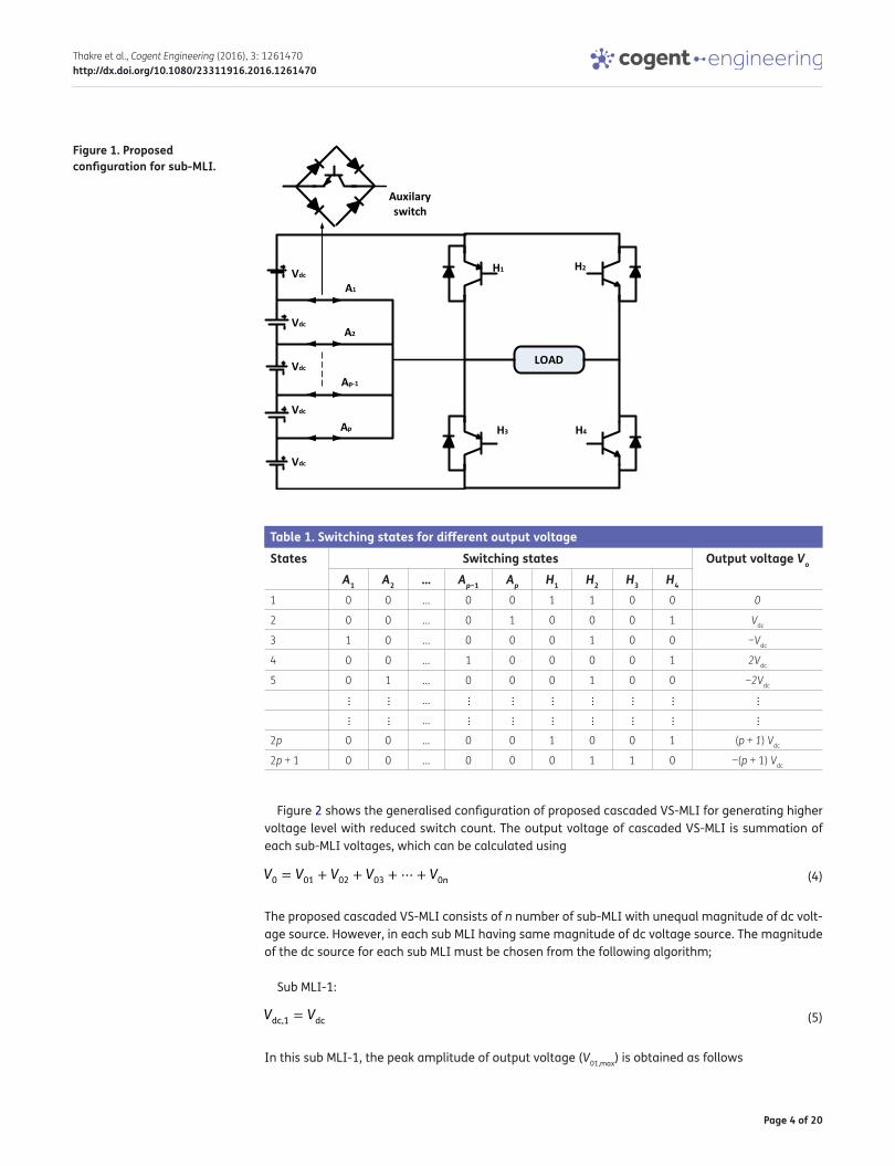
2. Proposed configurationThe proposed configuration for a voltage source multilevel inverter is shown in Figure 1. This configu-ration consists of one H-bridge and a basic unit cell. The basic unit contains p bidirectional auxiliary switches, which have been presented in Gautam, Gupta, and Kumar (2015), Gautam, Gupta, and Sahu (2016), Odeh and Agu (2016), Raushan, Mahato, and Jana (2016) and (p + 1) dc sources.
Table 1 shows the look-up table for switching states for different output voltage in proposed sub-MLI; its magnitude of isolated dc source is uniform. Therefore, this MLI is called symmetric VS-MLI. In the proposed configuration the number of output voltage levels, number of switches and gate drivers can be calculated as follows.
where p is the number of auxiliary switches in the basic unit. In the proposed VS-MLI the maximum output voltage V0,max is
(1)NLEVEL = 2p + 3
(2)NSWITCH = NMOSFET = NDRIVER = p + 4
(3)V0,max = (p + 1)Vdc
Page 4 of 20
Thakre et al., Cogent Engineering (2016), 3: 1261470http://dx.doi.org/10.1080/23311916.2016.1261470
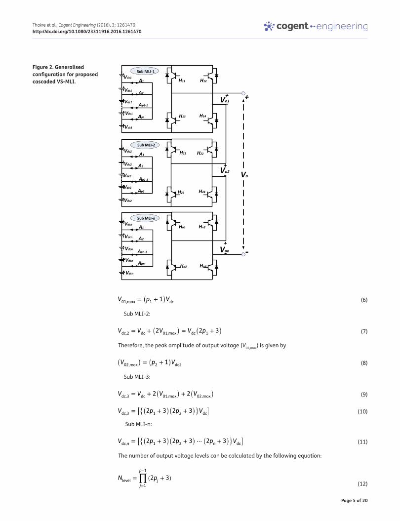
Figure 2 shows the generalised configuration of proposed cascaded VS-MLI for generating higher voltage level with reduced switch count. The output voltage of cascaded VS-MLI is summation of each sub-MLI voltages, which can be calculated using
The proposed cascaded VS-MLI consists of n number of sub-MLI with unequal magnitude of dc volt-age source. However, in each sub MLI having same magnitude of dc voltage source. The magnitude of the dc source for each sub MLI must be chosen from the following algorithm;
Sub MLI-1:
In this sub MLI-1, the peak amplitude of output voltage (V01,max) is obtained as follows
(4)V0 = V01 + V02 + V03 +⋯ + V0n
(5)Vdc,1 = Vdc
Figure 1. Proposed configuration for sub-MLI.
Table 1. Switching states for different output voltageStates Switching states Output voltage Vo
A1 A2 … Ap−1 Ap H1 H2 H3 H4
1 0 0 … 0 0 1 1 0 0 0
2 0 0 … 0 1 0 0 0 1 Vdc
3 1 0 … 0 0 0 1 0 0 −Vdc
4 0 0 … 1 0 0 0 0 1 2Vdc
5 0 1 … 0 0 0 1 0 0 −2Vdc
⋮ ⋮ … ⋮ ⋮ ⋮ ⋮ ⋮ ⋮ ⋮
⋮ ⋮ … ⋮ ⋮ ⋮ ⋮ ⋮ ⋮ ⋮
2p 0 0 … 0 0 1 0 0 1 (p + 1) Vdc
2p + 1 0 0 … 0 0 0 1 1 0 −(p + 1) Vdc
Page 5 of 20
Thakre et al., Cogent Engineering (2016), 3: 1261470http://dx.doi.org/10.1080/23311916.2016.1261470
Sub MLI-2:
Therefore, the peak amplitude of output voltage (V02,max) is given by
Sub MLI-3:
Sub MLI-n:
The number of output voltage levels can be calculated by the following equation:
(6)V01,max =(
p1 + 1)
Vdc
(7)Vdc,2 = Vdc +(
2V01,max)
= Vdc(
2p1 + 3)
(8)(
V02,max)
=(
p2 + 1)
Vdc2
(9)Vdc,3 = Vdc + 2(
V01,max)
+ 2(
V02,max)
(10)Vdc,3 =[(
2p1 + 3)(
2p2 + 3)
Vdc]
(11)Vdc,n =[(
2p1 + 3)(
2p2 + 3)
⋯(
2pn + 3)
Vdc]
(12)Nlevel =
p−1∏
j=1
(2pj + 3)
Figure 2. Generalised configuration for proposed cascaded VS-MLI.
Page 6 of 20
Thakre et al., Cogent Engineering (2016), 3: 1261470http://dx.doi.org/10.1080/23311916.2016.1261470
In the proposed configuration, the number of power switches including auxiliary switches and unidi-rectional switches is given by
By using the proposed algorithm, the maximum amplitude of the output voltage (V0,max) is expressed, as follows:
3. Optimal configuration
3.1. Maximum number of voltage levels with constant number of switchesThe main objective of a multilevel inverter is to generate higher voltage levels with minimum num-ber of switches. The product of number of voltage levels, whose sum is constant, when the numbers of auxiliary switches are same in each basic unit.
Using (13) and (15) can write
The value of p must be determined. Using (12) and (15), the maximum number of output voltage level will be determined as follows:
Considering (16) and (17), can express
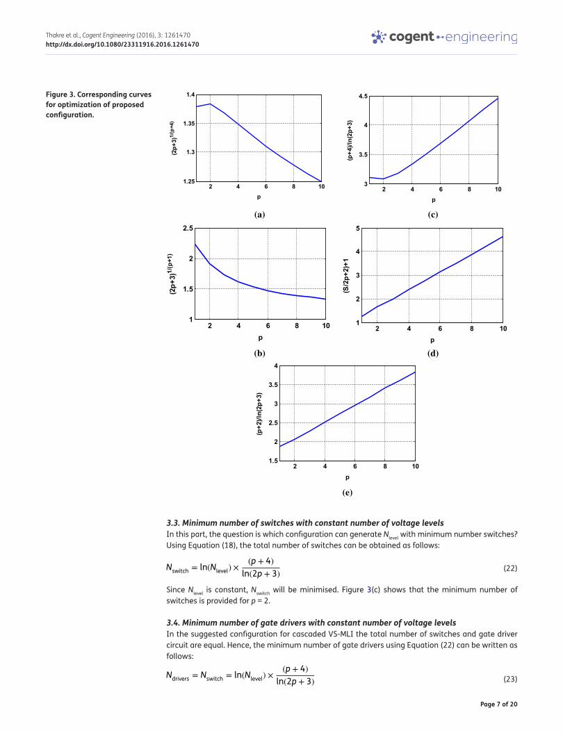
Figure 3(a) shows the variation of (2p + 3)1/(p + 4) vs. p. It clear that maximum number of output volt-age levels is obtained for p = 2. Thus, cascaded VS-MLI consisting of two auxiliary switches can pro-duce the maximum output voltage levels.
3.2. Maximum number of voltage levels with constant number of isolated dc sourcesAs seen from Figure 2, the proposed configuration consist of n sub MLIs and each of them consist of (pn + 1) isolated dc sources (j = 1, 2, … , n). Thus, the number of dc sources can be obtained by:
Using (17) and (20), the maximum number of output voltage levels can be written as:
Figure 3(b) shows the variation of (2p + 3)1/(p + 1) vs. p. Thus, the configuration consisting of sub MLIs with one dc source can generate maximum output voltage levels.
(13)Nswitches = (p1 + p2 + p3 +⋯ + pn) + 4n
(14)V0,max =
n∑
j=1
(pj + 1) + Vj
(15)p1 = p2 = ⋯ = pn = p
(16)Nswitchp + 4
= n
(17)Nlevel = (2p + 3)n
(18)Nlevel =[
(2p + 3)1
(p+4)
]Nswitch
(19)Nsource = (p1 + 1) + (p2 + 1) +⋯ + (pn + 1) =
n∑
i=1
(pn + 1)
(20)Nsource = (p + 1)n
(21)Nlevel =[
(2p + 3)1∕(p+1)]Nsource
Page 7 of 20
Thakre et al., Cogent Engineering (2016), 3: 1261470http://dx.doi.org/10.1080/23311916.2016.1261470
3.3. Minimum number of switches with constant number of voltage levelsIn this part, the question is which configuration can generate Nlevel with minimum number switches? Using Equation (18), the total number of switches can be obtained as follows:
Since Nlevel is constant, Nswitch will be minimised. Figure 3(c) shows that the minimum number of switches is provided for p = 2.
3.4. Minimum number of gate drivers with constant number of voltage levelsIn the suggested configuration for cascaded VS-MLI the total number of switches and gate driver circuit are equal. Hence, the minimum number of gate drivers using Equation (22) can be written as follows:
(22)Nswitch = ln(Nlevel) ×(p + 4)
ln(2p + 3)
(23)Ndrivers = Nswitch = ln(Nlevel) ×(p + 4)
ln(2p + 3)
Figure 3. Corresponding curves for optimization of proposed configuration.
(c)(a)
(d)(b)
(e)
2 4 6 8 101.25
1.3
1.35
1.4
p
(2p+3)1/(p+4)
2 4 6 8 103
3.5
4
4.5
p
(p+4)/ln(2p+3)
2 4 6 8 101
1.5
2
2.5
p
(2p+3)1/(p+1)
2 4 6 8 101
2
3
4
5
p(S/2p+2)+1
2 4 6 8 101.5
2
2.5
3
3.5
4
p
(p+2)/ln(2p+3)
Page 8 of 20
Thakre et al., Cogent Engineering (2016), 3: 1261470http://dx.doi.org/10.1080/23311916.2016.1261470
3.5. Minimum blocking voltage across the switches with constant number of voltage levelsAn essential problem in multilevel inverters is the rating of circuit switches. In all MLIs, current through all switches are same as rated load current. But, this is not for the voltage across the switch-es. The aim is to find the configuration for cascaded VS-MLI with minimum blocking voltage which can generate constant number of output voltage levels. The maximum magnitude of blocking volt-age (Vswitch) is expressed as follows:
where Vswitch,A and Vswitch,B are the maximum magnitude of blocking voltage across the auxiliary and unidirectional switches, respectively. Also Vswitch,a,j and Vswitch,b,j shows the maximum value of blocking voltage across auxiliary switches in jth sub MLI and unidirectional switches in the jth H-bridge, re-spectively. Hence, Equation (25) can be considered as a criterion to compare different MLIs from the view point of the peak value across the switches (Babaei, 2008; Ebrahimi et al., 2012; Shalchi Alishah et al., 2015). The lower value of the criterion indicates that a minimum voltage across the switches. As conclude from Figure 2, peak value of blocking voltage across the auxiliary switches in jth sub MLI can be expressed, as follows:
Therefore, the peak value of the blocking voltage across the auxiliary switches can be calculated, as follows:
In the Equations (26) and (27), S is determined by the following expression:
From (5)–(12), (15), (27) and (28), the maximum voltage across auxiliary switches in basic units can be written as follows:
The maximum value of the blocking voltage across the unidirectional switches in the jth H-bridges can be given as follows:
(24)Vswitch = Vswitch,A + Vswitch,B
(25)Vswitch =
n∑
i=1
Vswitch,A,j +
n∑
i=1
Vswitch,b,j
(26)Vswitch,A,j = S × Vj , j = 1, 2,… ,n
(27)Vswitch,A,j = S × (Vdc,1 + Vdc,2 +⋯ + Vdc,n)
(28)S = 2
[
p + (p − 1) + (p − 2) +⋯ +
p −(p − 3)
2
]
+p + 1
2=3p2 + 2p − 1
4(if p is an odd number)
(29)S = 2
[
p + (p − 1) + (p − 2) +⋯ +
p −(p − 2)
2
]
=3p2 + 2p
4
(if p is an even number)
(30)Vswitch,A = S[
1 + (2p + 3) +⋯ + (2p + 3)n−1]
× Vdc
(31)Vswitch,A = S(Nlevel − 1)
2p + 2× Vdc
(32)Vswitch,b,j = 2
n∑
i=1
Vji = 2 × (p + 1) × (2p + 2)j−1 × Vdc
Page 9 of 20
Thakre et al., Cogent Engineering (2016), 3: 1261470http://dx.doi.org/10.1080/23311916.2016.1261470
The maximum value of blocking voltage across the H-bridge switches can be expressed as follows:
Hence, the MBV across all the switches of proposed configuration using (24) can be expressed, as follows:
The curve is drawn between S/(2p + 2)+1 and p is shown in Figure 3(d). As seen this curve, Vswitch is minimum at (p = 1) for proposed cascaded MLI.
3.6. Minimum number of ON-state switches with constant number of voltage levelsIn the proposed configuration, the number of ON-state switches (NON-SS) can be calculated by:
Using (15)–(17) and (35), the number of ON-state switches is given as follows:
As shown in Figure 3(e), the minimum number of ON-state switches to generate maximum number of output voltage levels is obtained for p = 1.
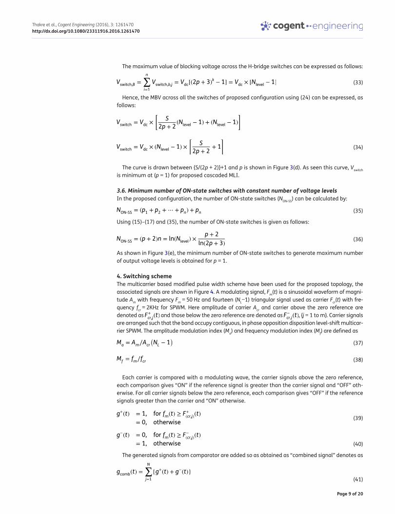
4. Switching schemeThe multicarrier based modified pulse width scheme have been used for the proposed topology, the associated signals are shown in Figure 4. A modulating signal, Fm(t) is a sinusoidal waveform of magni-tude Am with frequency Fm = 50 Hz and fourteen (NL−1) triangular signal used as carrier Fcr(t) with fre-quency fcr = 2KHz for SPWM. Here amplitude of carrier Acr and carrier above the zero reference are denoted as F+cr,j(t) and those below the zero reference are denoted as F−cr,j(t), j = 1 to m. Carrier signals are arranged such that the band occupy contiguous, in phase opposition disposition level-shift multicar-rier SPWM. The amplitude modulation index (Ma) and frequency modulation index (Mf) are defined as
Each carrier is compared with a modulating wave, the carrier signals above the zero reference, each comparison gives “ON” if the reference signal is greater than the carrier signal and “OFF” oth-erwise. For all carrier signals below the zero reference, each comparison gives “OFF” if the reference signals greater than the carrier and “ON” otherwise.
The generated signals from comparator are added so as obtained as “combined signal” denotes as
(33)Vswitch,B =
n∑
i=1
Vswitch,b,j = Vdc[(2p + 3)k − 1] = Vdc × [Nlevel − 1]
Vswitch = Vdc ×
[
S
2p + 2(Nlevel − 1) + (Nlevel − 1)
]
(34)Vswitch = Vdc × (Nlevel − 1) ×
[
S
2p + 2+ 1
]
(35)NON-SS = (p1 + p2 +⋯ + pn) + pn
(36)NON-SS = (p + 2)n = ln(Nlevel) ×p + 2
ln(2p + 3)
(37)Ma = Am∕Acr(
NL − 1)
(38)Mf = fm∕fcr
(39)g+(t) = 1, for fm(t) ≥ F+(cr,j)(t)
= 0, otherwise
(40)g−(t) = 0, for fm(t) ≥ F−(cr,j)(t)
= 1, otherwise
(41)gcomb(t) =
N∑
j=1
g+(t) + g−(t)
Page 10 of 20
Thakre et al., Cogent Engineering (2016), 3: 1261470http://dx.doi.org/10.1080/23311916.2016.1261470
The combination signal “gcomb(t)” that acquires the same wave shape as that of the staircase out-put voltage waveform is shown in Figure 4, the actual switching signals are obtained from combined signal by comparing the desired level signals and generated look-up table.
5. Calculation of lossesThe reduction in the number of switches has a significant effect on the inverter losses as the conduc-tion loss depends on ON-state voltage drop of power switches and equivalent resistance and the switching losses depend on the non-ideal operation of power switches. The power losses are calcu-lated as follows.
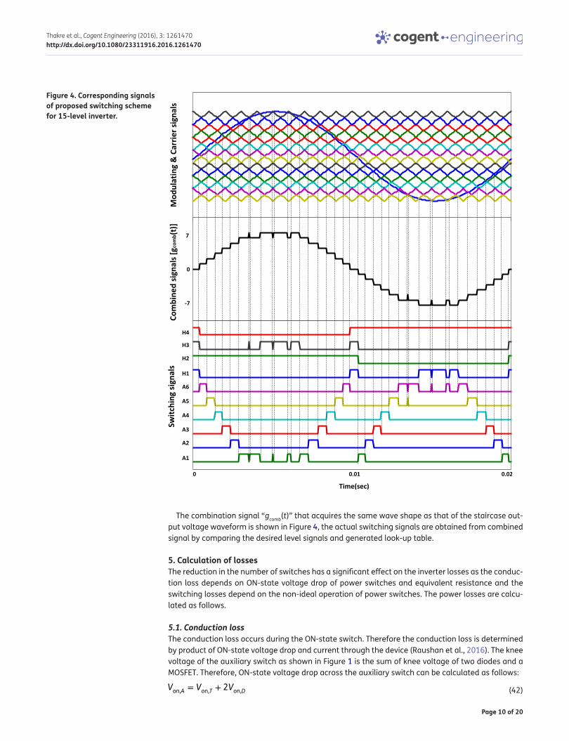
5.1. Conduction lossThe conduction loss occurs during the ON-state switch. Therefore the conduction loss is determined by product of ON-state voltage drop and current through the device (Raushan et al., 2016). The knee voltage of the auxiliary switch as shown in Figure 1 is the sum of knee voltage of two diodes and a MOSFET. Therefore, ON-state voltage drop across the auxiliary switch can be calculated as follows:
(42)Von,A = Von,T + 2Von,D
Figure 4. Corresponding signals of proposed switching scheme for 15-level inverter.
Page 11 of 20
Thakre et al., Cogent Engineering (2016), 3: 1261470http://dx.doi.org/10.1080/23311916.2016.1261470
where VT and RT are ON-state voltage and the equivalent resistance of MOSFET, respectively. β is a constant dependent on MOSFET parameters. VD and RD represents ON-state voltage and resistance of the diode, respectively. If the MLI operating at large number of voltage level, the load current can be assumed is almost as a sinusoidal. The instantaneous conduction loss (Pc,A(t)) can be given as:
In the proposed VS-MLI, p numbers of auxiliary switches are present accompanied by H-bridge uni-directional switches i.e. MOSFET with body diode. Hence, the instantaneous conduction loss of the unidirectional switches (Pc,U(t)) can be calculated as
To calculates the total conduction loss, it is required to define the switches count, NS(t) and diodes, ND(t) at any instant in H-bridge. It is noticeable that, output voltage level and operating conditions (in the current direction) affect the quantity of ON-state switches that is time-variant. Considering (PCn,A(t)) as instantaneous conduction loss of nth auxiliary switch, The average conduction losses are written as follows
5.2. Switching lossesTo calculate the total switching loss of the proposed inverter, the energy loss during ON and OFF-state of a typical power switch with the body diode is considered first and then that amount is ap-plied to the proposed inverter. Suppose that the voltage and current varies linearly during ON and OFF time a switch can be expressed as follows.
where Eon and Eoff are ON-state and OFF-state loss energy and ton and toff are the ON and OFF-state period of the switch respectively. I is the current through the switch and Vsw is voltage across the switch before turned-OFF or turned-ON. The total switching loss can be obtained as follows.
where f is the fundamental frequency. Non is the number of ON-states and Noff is the number of OFF-states. The total power losses of proposed inverter can be obtained using (46) and (49) as
(43)Von,A = [(VT + I⋅ RT) + 2(VD + RD.I)]
(44)Pc,A(t) =[
VT + 2VDIo sin(t) + 2RDI2o ⋅ sin(t) + RT ⋅ I
+1o sin
+1(t)
]
(45)Pc,U(t) =[
NT(t)VT + ND(t)VDIo ⋅ sin(t) + ND(t)RDI2o sin
2(t) + RTI
+1o sin
+1(t)
]
(46)PC,Avg =1
p∑
n=1
∫0
[Pcn,A(t)]dt +1
∫0
[Pc,U(t)]dt
Eon =
ton
∫0
v(t)i(t)dt
(47)=
ton
∫0
[(
Vswton
t
)(
−I
ton
(
t − ton)
)]
dt =1
6VswIton
Eoff =
toff
∫0
v(t)i(t)dt
(48)
toff
∫0
[(
Vswtoff
t
)(
−I
toff
(
t − toff)
)]
dt =1
6VswItoff
(49)Psw = f (NonEon + NoffEoff)
Page 12 of 20
Thakre et al., Cogent Engineering (2016), 3: 1261470http://dx.doi.org/10.1080/23311916.2016.1261470
In this study, following parameters are considered to determine the power loss of proposed cas-caded VS-MLI:
RT = 0.25 Ω, RD = 0.11 Ω VT = 2.5 V, VD = 1.2 V, β = 1, ton = toff = 1 μs, f = 50 Hz. Each isolated DC volt-age source has magnitude 12 V. The load resistance is 15 Ω. The mathematical calculation is carried out for each switch (MOSFET) for one cycle using Equations (42)–(50) and total power loss for one second is obtained as 3.624 mW.
(50)Total power losses,(
PLoss)
= PC,Avg + Psw
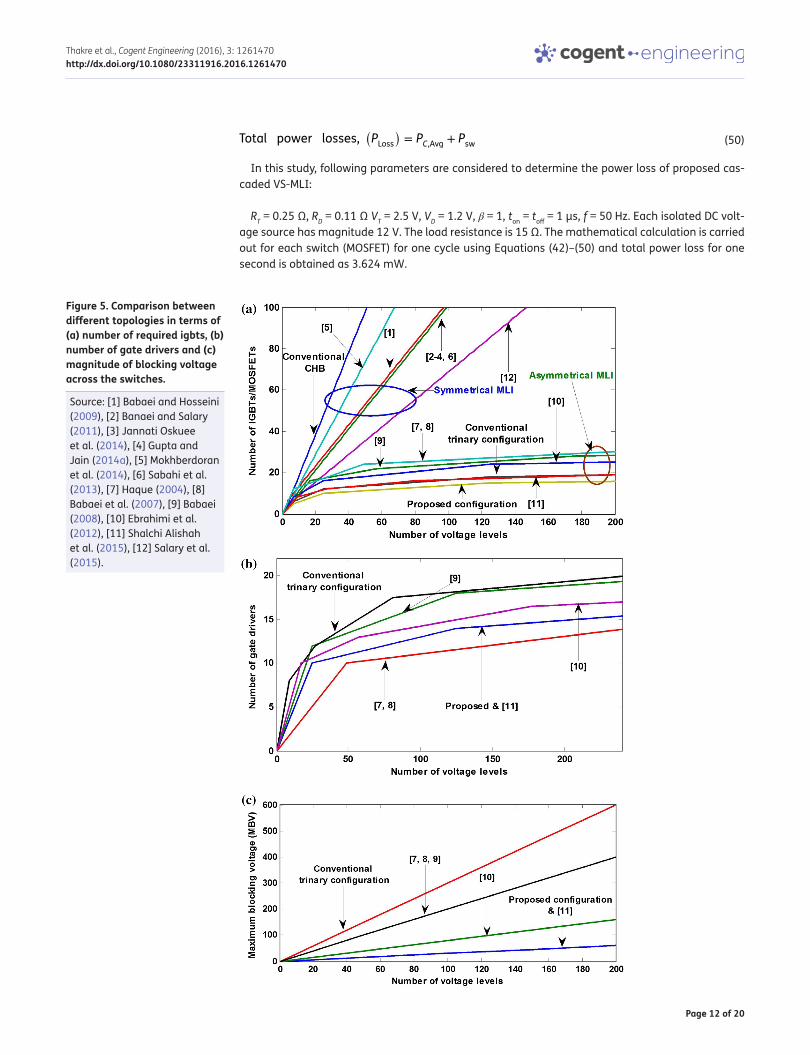
Figure 5. Comparison between different topologies in terms of (a) number of required igbts, (b) number of gate drivers and (c) magnitude of blocking voltage across the switches.
Source: [1] Babaei and Hosseini (2009), [2] Banaei and Salary (2011), [3] Jannati Oskuee et al. (2014), [4] Gupta and Jain (2014a), [5] Mokhberdoran et al. (2014), [6] Sabahi et al. (2013), [7] Haque (2004), [8] Babaei et al. (2007), [9] Babaei (2008), [10] Ebrahimi et al. (2012), [11] Shalchi Alishah et al. (2015), [12] Salary et al. (2015).
Page 13 of 20
Thakre et al., Cogent Engineering (2016), 3: 1261470http://dx.doi.org/10.1080/23311916.2016.1261470
6. Comparative studyIn this section, the proposed cascaded VS-MLI has compared with similar asymmetric structure (Babaei, 2008; Babaei et al., 2007; Ebrahimi et al., 2012; Haque, 2004; Shalchi Alishah et al., 2015) and some of symmetrical structure (Babaei & Hosseini, 2009; Banaei & Salary, 2011; Gupta & Jain, 2014a; Jannati Oskuee et al., 2014; Mokhberdoran et al., 2014; Sabahi et al., 2013; Shalchi Alishah et al., 2015) in terms of the number of IGBTs/MOSFETs, gate drivers and MBV across the switches. The com-parison between proposed configuration for cascaded VS-MLI and configurations presented in Babaei (2008), Babaei and Hosseini (2009), Babaei et al. (2007), Banaei and Salary (2011), Ebrahimi et al. (2012), Gupta and Jain (2014a), Haque (2004), Jannati Oskuee et al. (2014), Mokhberdoran et al. (2014), Sabahi et al. (2013), Shalchi Alishah et al. (2015) are shown in Figure 5(a). This figure indicates that the proposed configuration requires less number of IGBTs/MOSFETs for same voltage levels com-pared to other topologies for both symmetrical and asymmetrical structures. Figure 5(b) shows the comparison between gate drivers and number of voltage levels. As conclude from the figure, the proposed configuration and topology presented in Shalchi Alishah et al. (2015) requires fewer gate
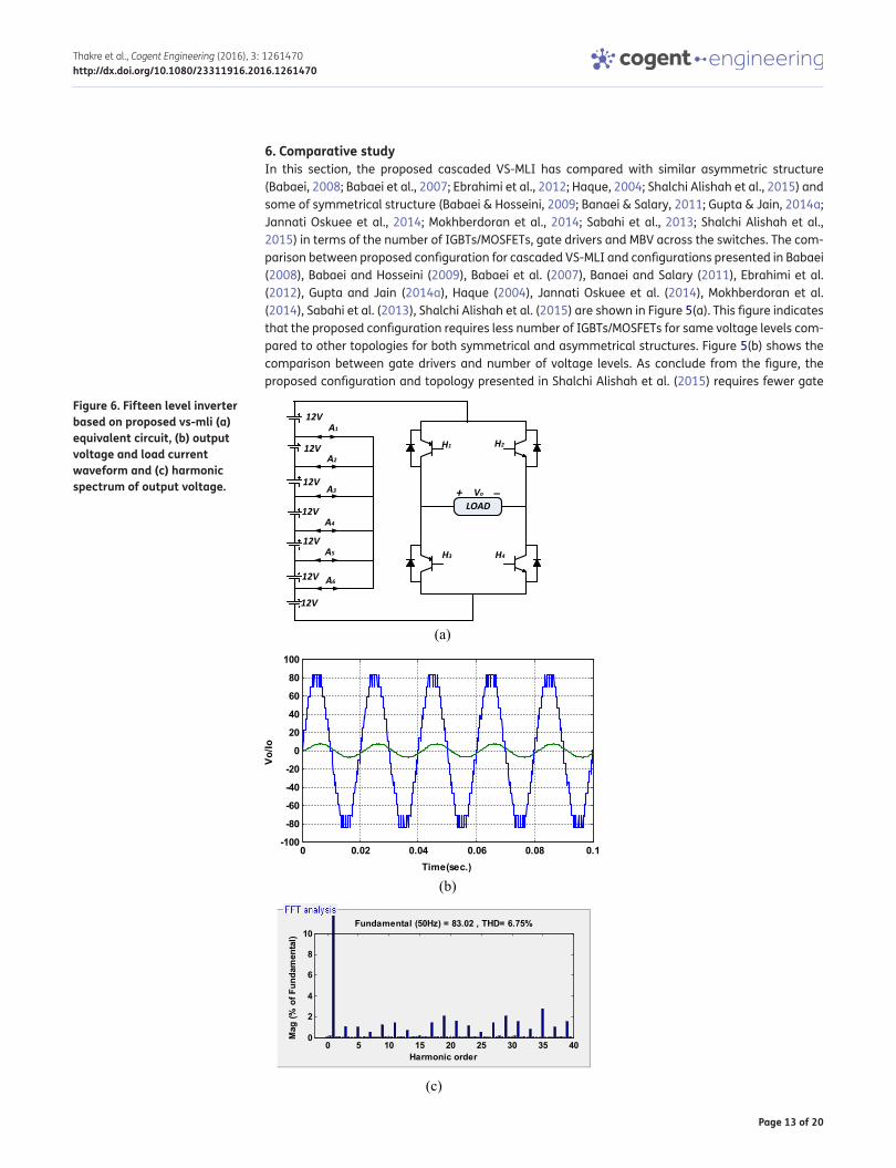
Figure 6. Fifteen level inverter based on proposed vs-mli (a) equivalent circuit, (b) output voltage and load current waveform and (c) harmonic spectrum of output voltage.
Page 14 of 20
Thakre et al., Cogent Engineering (2016), 3: 1261470http://dx.doi.org/10.1080/23311916.2016.1261470
drivers. However, other presented topologies in Babaei (2008), Babaei et al. (2007) needs few lesser than the proposed one. Figure 5(c) shows the comparison between different structures based on magnitude of blocking voltage on the switches. According to this figure the magnitude of blocking voltage in proposed configuration and topology presented in Shalchi Alishah et al. (2015) are lower than the topologies in Babaei (2008), Babaei et al. (2007), Ebrahimi et al. (2012), Haque (2004).
7. Results and discussionTo verify the performance of proposed configurations, the simulation using MATLAB Simulink envi-ronment and experimental studies are presented, for 15-level inverter based on single sub-MLI as shown in Figure 1 and 25-level inverter using cascaded VS-MLI as shown in Figure 2.
7.1. Simulation resultsThe equivalent circuit of 15-level inverter of proposed configuration is depicted in Figure 6(a), the circuit consist of six auxiliary, four unidirectional switches and seven DC sources with the magnitude of 12 V, which produce the staircase voltage waveform of maximum output voltage 84 V. A series
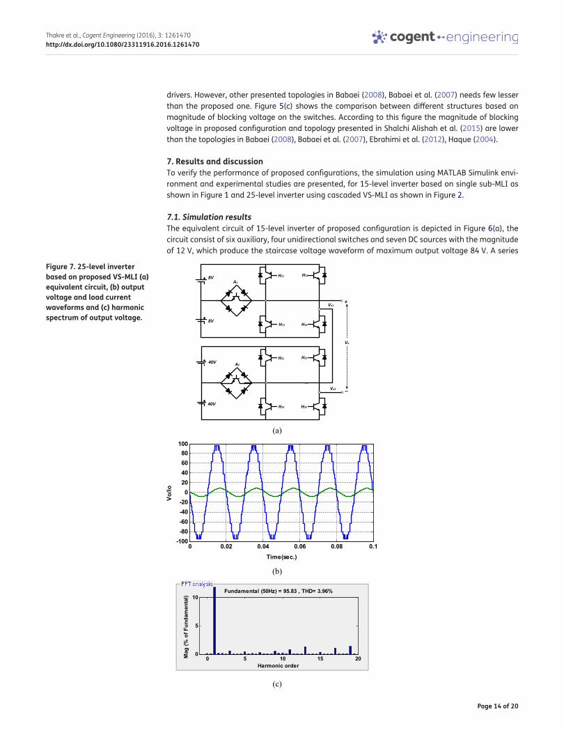
Figure 7. 25-level inverter based on proposed VS-MLI (a) equivalent circuit, (b) output voltage and load current waveforms and (c) harmonic spectrum of output voltage.
Page 15 of 20
Thakre et al., Cogent Engineering (2016), 3: 1261470http://dx.doi.org/10.1080/23311916.2016.1261470
R-L branch (R = 15 Ω and L = 20 mH) considered as load parameters for all cases. The waveforms of output voltage and load current of the 15-level inverter are shown in Figure 6(b), harmonic spectrum of the 15-level output voltage is shown in Figure 6(c). Another 25-level inverter based on cascaded VS-MLI configuration has been implemented as shown in Figure 7(a). The 25-level inverter requires only two auxiliary switches and four DC supplies with magnitude of V1 = 8 V and V2 = 40 V. This pro-posed 25-level inverter generates maximum output voltage of 96 V, 3.96% THD. The waveforms of output voltage and load current of the 25-level inverter are shown in Figure 7(b), harmonic spectrum of the output voltage is shown in Figure 7(c).
7.2. Experimental resultsTo validate the simulation and effectiveness of the proposed configuration, a prototype of proposed single phase 15-level and 25-level inverter have been developed in the laboratory. The hardware
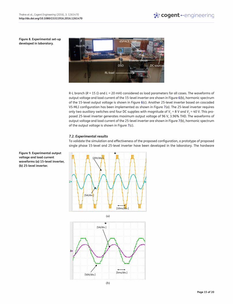
Figure 8. Experimental set-up developed in laboratory.
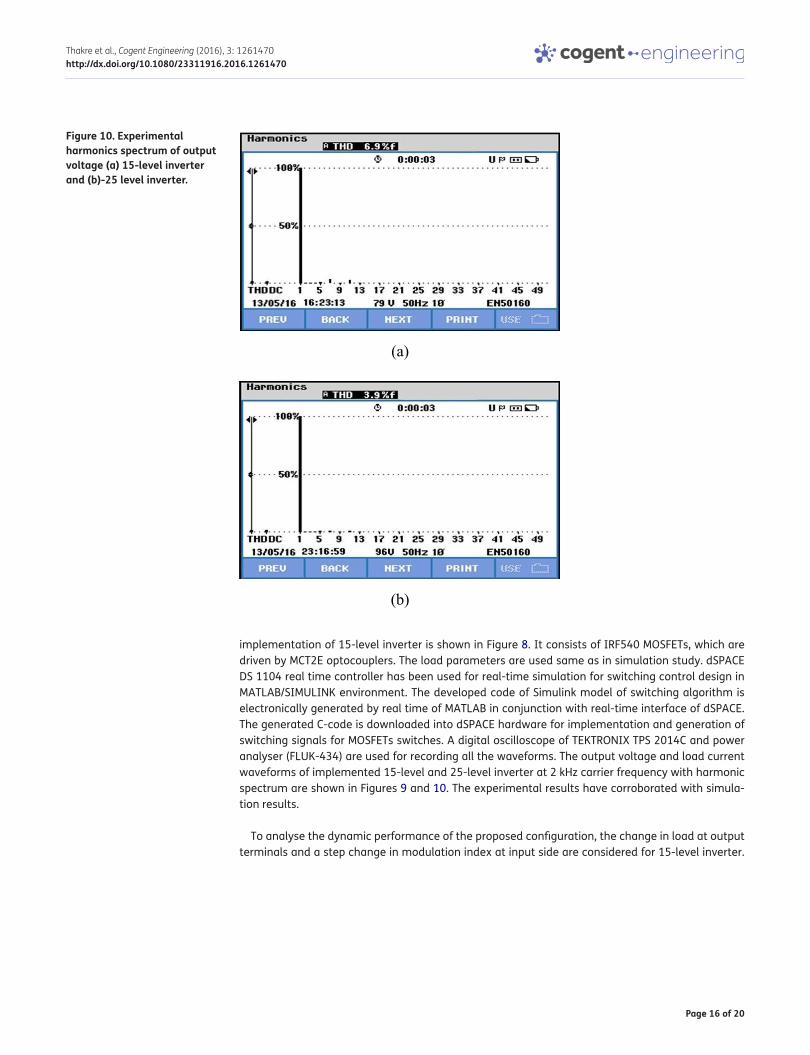
Figure 9. Experimental output voltage and load current waveforms (a) 15-level inverter, (b) 25-level inverter.
Page 16 of 20
Thakre et al., Cogent Engineering (2016), 3: 1261470http://dx.doi.org/10.1080/23311916.2016.1261470
implementation of 15-level inverter is shown in Figure 8. It consists of IRF540 MOSFETs, which are driven by MCT2E optocouplers. The load parameters are used same as in simulation study. dSPACE DS 1104 real time controller has been used for real-time simulation for switching control design in MATLAB/SIMULINK environment. The developed code of Simulink model of switching algorithm is electronically generated by real time of MATLAB in conjunction with real-time interface of dSPACE. The generated C-code is downloaded into dSPACE hardware for implementation and generation of switching signals for MOSFETs switches. A digital oscilloscope of TEKTRONIX TPS 2014C and power analyser (FLUK-434) are used for recording all the waveforms. The output voltage and load current waveforms of implemented 15-level and 25-level inverter at 2 kHz carrier frequency with harmonic spectrum are shown in Figures 9 and 10. The experimental results have corroborated with simula-tion results.
To analyse the dynamic performance of the proposed configuration, the change in load at output terminals and a step change in modulation index at input side are considered for 15-level inverter.
Figure 10. Experimental harmonics spectrum of output voltage (a) 15-level inverter and (b)-25 level inverter.
Page 17 of 20
Thakre et al., Cogent Engineering (2016), 3: 1261470http://dx.doi.org/10.1080/23311916.2016.1261470
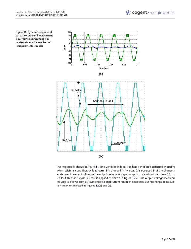
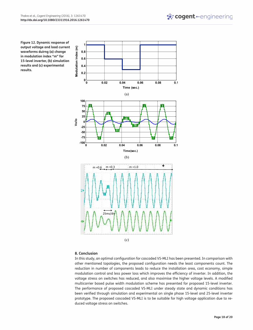
The response is shown in Figure 11 for a variation in load. The load variation is obtained by adding extra resistance and thereby load current is changed in inverter. It is observed that the change in load current does not influence the output voltage. A step change in modulation index (m = 0.6 and 0.3 for 0.02 s) in 1 cycle (20 ms) is applied as shown in Figure 12(a). The output voltage levels are reduced to 5-level from 15-level and also load current has been decreased during change in modula-tion index as depicted in Figures 12(b) and (c).
Figure 11. Dynamic response of output voltage and load current waveforms during change in load (a) simulation results and (b)experimental results
Page 18 of 20
Thakre et al., Cogent Engineering (2016), 3: 1261470http://dx.doi.org/10.1080/23311916.2016.1261470
8. ConclusionIn this study, an optimal configuration for cascaded VS-MLI has been presented. In comparison with other mentioned topologies, the proposed configuration needs the least components count. The reduction in number of components leads to reduce the installation area, cost economy, simple modulation control and less power loss which improves the efficiency of inverter. In addition, the voltage stress on switches has reduced, and also maximise the higher voltage levels. A modified multicarrier based pulse width modulation scheme has presented for proposed 15-level inverter. The performance of proposed cascaded VS-MLI under steady state and dynamic conditions has been verified through simulation and experimental on single phase 15-level and 25-level inverter prototype. The proposed cascaded VS-MLI is to be suitable for high voltage application due to re-duced voltage stress on switches.
Figure 12. Dynamic response of output voltage and load current waveforms duirng (a) change in modulation index “m” for 15-level inverter, (b) simulation results and (c) experimental results.
Page 19 of 20
Thakre et al., Cogent Engineering (2016), 3: 1261470http://dx.doi.org/10.1080/23311916.2016.1261470
FundingThe author received no direct funding for this research.
Author detailsKishor Thakre1
E-mail: [email protected] Barada Mohanty1
E-mail: [email protected] Sagar Kommukuri1
E-mail: [email protected] Chatterjee1
E-mail: [email protected] Department of Electrical Engineering, National Institute of
Technology Rourkela, Odisha 769008, India.
Citation informationCite this article as: Optimal configuration for cascaded voltage source multilevel inverter based on series connection sub-multilevel inverter, Kishor Thakre, Kanungo Barada Mohanty, Vinaya Sagar Kommukuri & Aditi Chatterjee, Cogent Engineering (2016), 3: 1261470.
ReferencesAzeez, N. A., Dey, A., Mathew, K., & Mathew, J. (2014). A
medium-voltage inverter-fed IM drive using multilevel 12-sided polygonal vectors, with nearly constant switching frequency current hysteresis controller. IEEE Transactions on Industrial Electronics, 61, 1700–1709. http://dx.doi.org/10.1109/TIE.2013.2266083
Babaei, E. (2008). A cascade multilevel converter topology with reduced number of switches. IEEE Transactions on Power Electronics, 23, 2657–2664. http://dx.doi.org/10.1109/TPEL.2008.2005192
Babaei, E., & Gowgani, S. S. (2014). Hybrid multilevel inverter using switched capacitor units. IEEE Transactions on Industrial Electronics, 61, 4614–4621. http://dx.doi.org/10.1109/TIE.2013.2290769
Babaei, E., & Hosseini, S. H. (2009). New cascaded multilevel inverter topology with minimum number of switches. Energy Conversion and Management, 50, 2761–2767. http://dx.doi.org/10.1016/j.enconman.2009.06.032
Babaei, E., Hosseini, S. H., Gharehpetian, G. B., Haque, M. T., & Sabahi, M. (2007). Reduction of DC voltage sources and switches in asymmetrical multilevel converters using a novel topology. International Journal of Electrical Power & Energy Systems, 77, 1073–1085.
Banaei, M. R., & Salary, E. (2011). Verification of new family for cascade multilevel inverters with reduction of components. Journal of Electrical Engineering and Technology, 6, 245–254. http://dx.doi.org/10.5370/JEET.2011.6.2.245
Buticchi, G., Barater, D., Lorenzani, E., Concari, C., & Franceschini, G. (2014). A nine-level grid-connected converter topology for single-phase transformerless PV systems. IEEE Transactions on Industrial Electronics, 61, 3951–3960. http://dx.doi.org/10.1109/TIE.2013.2286562
Ceglia, G., Guzman, V., Sanchez, C., Ibanez, F., Walter, J., & Gimenez, M. I. (2006). A new simplified multilevel inverter topology for DC & AC conversion. IEEE Transactions on Power Electronics, 21, 1311–1319. http://dx.doi.org/10.1109/TPEL.2006.880303
Chavarria, J., Biel, D., & Guinjoan, F. (2013). Energy-balance control of PV cascaded multilevel grid-connected inverters under level-shifted and phase-shifted PWMs. IEEE Transactions on Industrial Electronics, 60, 98–111. http://dx.doi.org/10.1109/TIE.2012.2186108
Ebrahimi, J., Babaei, E., & Gharehpetian, G. B. (2012). A new multilevel converter topology with reduced number of power electronic components. IEEE Transactions on Industrial Electronics, 59, 655–667. http://dx.doi.org/10.1109/TIE.2011.2151813
Farokhnia, N., Fathi, S. H., Salehi, R., Gharehpetian, G. B., & Ehsani, M. (2012). Improved selective harmonic elimination pulse-width modulation strategy in multilevel inverters. IET Power Electronics, 5, 1904–1911. http://dx.doi.org/10.1049/iet-pel.2011.0293
Gautam, S. P., Gupta, S., & Kumar, L. (2015). Hybrid topology of symmetrical multilevel inverter using less number of devices. IET Power Electronics, 8, 2125–2135. http://dx.doi.org/10.1049/iet-pel.2015.0037
Gautam, S. P., Gupta, S., & Sahu, L. K. (2016). Reduction in number of devices for symmetrical and asymmetrical multilevel inverters. IET Power Electronics, 9, 698–709. http://dx.doi.org/10.1049/iet-pel.2015.0176
Gupta, K. K., & Jain, S. (2012). Topology for multilevel inverters to attain maximum number of levels from given DC sources. IET Power Electronics, 5, 435–446. http://dx.doi.org/10.1049/iet-pel.2011.0178
Gupta, K. K., & Jain, S. (2014a). Comprehensive review of a recently proposed multilevel inverter. IET Power Electronics, 7, 467–479. http://dx.doi.org/10.1049/iet-pel.2012.0438
Gupta, K. K., & Jain, S. (2014b). A novel multilevel inverter based on switched DC sources. IEEE Transactions on Industrial Electronics, 61, 3269–3278. http://dx.doi.org/10.1109/TIE.2013.2282606
Gupta, R., Ghosh, A., & Joshi, A. (2008). Switching characterization of cascaded multilevel-inverter-controlled systems. IEEE Transactions on Industrial Electronics, 55, 1047–1058. http://dx.doi.org/10.1109/TIE.2007.896274
Haque, M. T. (2004). Series sub-multilevel voltage source inverters (MLVSIs) as a high quality MLVSI. In Proc. SPEEDAM (pp. F1B-1–F1B-4). Capri.
Hinago, Y., & Koizumi, H. (2010). A single-phase multilevel inverter using switched series/parallel DC voltage sources. IEEE Transactions on Industrial Electronics, 57, 2643–2650. http://dx.doi.org/10.1109/TIE.2009.2030204
Jannati Oskuee, M. R., Banaei, M. R. J., & Khounjahan, H. (2014). Reconfiguration of semi-cascaded multilevel inverter to improve systems performance parameters. IET Power Electronics, 7, 1106–1112. http://dx.doi.org/10.1049/iet-pel.2013.0277
Khajehoddin, S. A., Bakhshai, A., & Jain, P. K. (2008). A simple voltage balancing scheme for m-level diode-clamped multilevel converters based on a generalized current flow model. IEEE Transactions on Power Electronics, 23, 2248–2259. http://dx.doi.org/10.1109/TPEL.2008.2001892
Lu, S., Marieethoz, S., & Corzine, K. A. (2010). Asymmetrical cascade multilevel converters with noninteger or dynamically changing dc voltage ratios: Concepts and modulation techniques. IEEE Transactions on Industrial Electronics, 57, 2411–2418.
McGrath, B. P., & Holmes, D. G. (2002). Multicarrier PWM strategies for multilevel inverters. IEEE Transactions on Industrial Electronics, 49, 858–867. http://dx.doi.org/10.1109/TIE.2002.801073
McGrath, B. P., & Holmes, D. G. (2008). Analytical modelling of voltage balance dynamics for a flying capacitor multilevel converter. IEEE Transactions on Power Electronics, 23, 543–550. http://dx.doi.org/10.1109/TPEL.2007.915175
Meshram, P., & Borghate, V. (2014). A simplified nearest level control (NLC) voltage balancing method for modular multilevel converter (MMC). IEEE Transactions on Power Electronics, 30, 450–462.
Mokhberdoran, A., Jannati Oskuee, M. R. J., Toopchi Khosroshahi, M. T., et al. (2014). Cascade multi-cell multilevel converter with reduced number of switches. IET Power Electronics, 7, 552–558. http://dx.doi.org/10.1049/iet-pel.2013.0261

Page 20 of 20
Thakre et al., Cogent Engineering (2016), 3: 1261470http://dx.doi.org/10.1080/23311916.2016.1261470
© 2016 The Author(s). This open access article is distributed under a Creative Commons Attribution (CC-BY) 4.0 license.You are free to: Share — copy and redistribute the material in any medium or format Adapt — remix, transform, and build upon the material for any purpose, even commercially.The licensor cannot revoke these freedoms as long as you follow the license terms.
Under the following terms:Attribution — You must give appropriate credit, provide a link to the license, and indicate if changes were made. You may do so in any reasonable manner, but not in any way that suggests the licensor endorses you or your use. No additional restrictions You may not apply legal terms or technological measures that legally restrict others from doing anything the license permits.
Cogent Engineering (ISSN: 2331-1916) is published by Cogent OA, part of Taylor & Francis Group. Publishing with Cogent OA ensures:• Immediate, universal access to your article on publication• High visibility and discoverability via the Cogent OA website as well as Taylor & Francis Online• Download and citation statistics for your article• Rapid online publication• Input from, and dialog with, expert editors and editorial boards• Retention of full copyright of your article• Guaranteed legacy preservation of your article• Discounts and waivers for authors in developing regionsSubmit your manuscript to a Cogent OA journal at www.CogentOA.com
Najafi, E., & Yatim, A. H. M. (2012). Design and implementation of a new multilevel inverter topology. IEEE Transactions on Industrial Electronics, 59, 4148–4154. http://dx.doi.org/10.1109/TIE.2011.2176691
Odeh, C. I., & Agu, V. N. (2016). Cascaded symmetrical series half-bridge cells multi-level inverter. Electric Power Components and Systems, 44, 1418–1427. http://dx.doi.org/10.1080/15325008.2016.1169464
Ounejjar, Y., Al-Haddad, K., & Gregoire, L. A. (2011). Packed U cells multilevel converter topology: Theoretical study and experimental validation. IEEE Transactions on Industrial Electronics, 58, 1294–1306. http://dx.doi.org/10.1109/TIE.2010.2050412
Rathore, A. K., Holtz, J., & Boller, T. (2013). Generalized optimal pulsewidth modulation of multilevel inverters for low-switching-frequency control of medium-voltage high-power industrial AC drives. IEEE Transactions on Industrial Electronics, 60, 4215–4224. http://dx.doi.org/10.1109/TIE.2012.2217717
Raushan, R., Mahato, B., & Jana, K. C. (2016). Comprehensive analysis of a novel three-phase multilevel inverter with minimum number of switches. IET Power Electronics, 9, 1600–1607. http://dx.doi.org/10.1049/iet-pel.2015.0682
Rech, C., & Pinheiro, J. R. (2007). Hybrid multilevel converters: Unified analysis and design considerations. IEEE Transactions on Industrial Electronics, 54, 1092–1104. http://dx.doi.org/10.1109/TIE.2007.892255
Rodriguez, J., Bernet, S., Wu, B., Pontt, J. O., & Kouro, S. (2007). Multilevel voltage source-converter topologies for industrial medium-voltage drives. IEEE Transactions on Industrial Electronics, 54, 2930–2945.
Rodriguez, J., Lai, J. S., & Peng, F. Z. (2002). Multilevel inverters: A survey of topologies, controls, and applications. IEEE Transactions on Industrial Electronics, 49, 724–738. http://dx.doi.org/10.1109/TIE.2002.801052
Sabahi, M. F., Babaei, E., & Farhadi Kangarlu, M. (2013). Cascaded cross-switched multilevel inverter in symmetric and asymmetric conditions. IET Power Electronics, 6, 1041–1050. http://dx.doi.org/10.1049/iet-pel.2012.0563
Salary, E., Jannati Oskuee, M. R., & Najafi-Ravadanegh, S. (2015). Creative design of symmetric multilevel converter to enhance the circuit’s performance. IET Power Electronics, 8, 96–102. http://dx.doi.org/10.1049/iet-pel.2013.0752
Shalchi Alishah, R. S., Nazarpour, D., Hosseini, S. H., & Sabahi, M. (2015). Reduction of power electronic elements in multilevel converters using a new cascade structure. IEEE Transactions on Industrial Electronics, 62, 256–269. http://dx.doi.org/10.1109/TIE.2014.2331012
Song, W., & Huang, A. Q. (2010). Fault-tolerant design and control strategy for cascaded H-bridge multilevel converter-based STATCOM. IEEE Transactions on Industrial Electronics, 57, 2700–2708. http://dx.doi.org/10.1109/TIE.2009.2036019
Sozer, Y., Hawes, N., Saha, A., Nguyen, H., & Torrey, D. A. (2014). Fast minimum loss space vector pulse-width modulation algorithm for multilevel inverters. IET Power Electronics, 7, 1590–1602. http://dx.doi.org/10.1049/iet-pel.2013.0423
Thakre, K., & Mohanty, K. B. (2015). Comparative analysis of THD for symmetrical and asymmetrical 17 level cascaded H-bridge inverter using carrier based PWM techniques. In Proceeding IEEE International Conference On Industrial Instrumentation and Control (pp. 306–310). Pune. doi:10.1109/IIC.2015.7150758
Veenstra, M., & Rufer, A. (2005). Control of a hybrid asymmetric multilevel inverter for competitive medium-voltage industrial drives. IEEE Transactions on Industry Applications, 41, 655–664. http://dx.doi.org/10.1109/TIA.2005.844382