Embed Size (px)
Citation preview
Optimisation of the preparation process
for tips used in scanning tunneling
microscopy
Diplomarbeit
zur Erlangung des akademischen Grades
Diplom-Physiker
vorgelegt von
Stefan Ernst
geboren am 02. Dezember 1980 in Leipzig
Max-Planck-Institut fur Chemische Physik fester Stoffe, Dresden
und
Fachrichtung Physik
Fakultat Mathematik und Naturwissenschaften
Technische Universitat Dresden
2006

Eingereicht am 26. Juni 2006
1. Gutachter: Prof. Dr. Frank Steglich
2. Gutachter: Prof. Dr. Lukas Eng
Abstract
The present work deals with the preparation and characterisation of tungsten tips for the
use in scanning tunnelling microscopy and spectroscopy (STM and STS, respectively). Elec-
trochemically etched tips require additional treatment to remove the dense oxide layer which
evolves during etching, and to further sharpen the tips. Facilities for in-situ tip conditioning
were implemented to two ultrahigh vacuum STM systems. The conditioning methods, in-
cluding direct resistive annealing, annealing by eletron bombardement, and self-sputtering
with noble gas ions, were tested. Tips were characterised by scanning electron microscopy,
field emission, and STM experiments. Using the so-prepared tips, high resolution STM
images and tunnelling spectra were obtained at room temperature and at low temperatures
(350 mK) on graphite, gold and niobium diselenide.
Zusammenfassung
Gegenstand der vorliegenden Arbeit ist die Herstellung und Charakterisierung von Wol-
framspitzen, welche eine wichtige Voraussetzung fur Rastertunnelmikroskopie (RTM) und
-spektroskopie darstellen. Die auf ublichem Wege elektrochemisch hergestellten Spitzen
bedurfen weiterer Bearbeitung, um die durch das Atzen unvermeidlich vorhandene Oxid-
schicht zu entfernen und die Spitzen weiter zu scharfen. Fur zwei bestehende Ultrahoch-
vakuum-RTM wurden die fur die in situ Spitzenbehandlung notwendigen mechanischen und
elektronischen Hilfsmittel aufgebaut und getestet. Dabei wurden die Spitzen mittels Ras-
terelektronenmikroskopie und Feldemissionsmessungen charakterisiert. Mit den durch re-
sistives Heizen, Elektronenstoßheizen sowie Selbst-Sputtern mit Edelgasionen bearbeiteten
Spitzen konnten hochaufgeloste RTM-Daten bei Raumtemperatur und bei tiefen Tempera-
turen auf Graphit, Gold sowie Niobdiselenid erzielt werden.

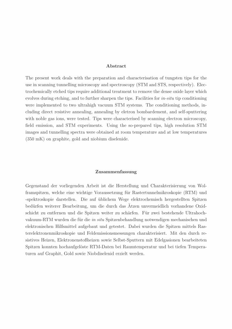
Wie schwer sind nicht die Mittel zu erwerben,
Durch die man zu den Quellen steigt!
J. W. von Goethe, Faust I

Contents
Contents . . . . . . . . . . . . . . . . . . . . . . . . . . . . . . . . . . . . . . . . . . . . . . . . . . . . . . . . . . . . . . . . . . . . 5
List of Figures . . . . . . . . . . . . . . . . . . . . . . . . . . . . . . . . . . . . . . . . . . . . . . . . . . . . . . . . . . . . . . . 7
List of Symbols and Abbreviations . . . . . . . . . . . . . . . . . . . . . . . . . . . . . . . . . . . . . . . . . . . . 9
1 Introduction . . . . . . . . . . . . . . . . . . . . . . . . . . . . . . . . . . . . . . . . . . . . . . . . . . . . . . . . . . . . . . 13
2 Basics of STM . . . . . . . . . . . . . . . . . . . . . . . . . . . . . . . . . . . . . . . . . . . . . . . . . . . . . . . . . . . 15
2.1 Quantum mechanical tunnelling . . . . . . . . . . . . . . . . . . . . . . . . . 15
2.2 The working principle of an STM . . . . . . . . . . . . . . . . . . . . . . . . 18
2.3 Instrumentation . . . . . . . . . . . . . . . . . . . . . . . . . . . . . . . . . . 21
2.3.1 The Variable Temperature STM (VT-STM) . . . . . . . . . . . . . . 21
2.3.2 The Cryogenic STM . . . . . . . . . . . . . . . . . . . . . . . . . . . 24
3 The preparation of tunnelling tips . . . . . . . . . . . . . . . . . . . . . . . . . . . . . . . . . . . . . . . . . 29
3.1 The role of the tunnelling tip . . . . . . . . . . . . . . . . . . . . . . . . . . 29
3.2 Electrochemical etching . . . . . . . . . . . . . . . . . . . . . . . . . . . . . . 32
3.3 Means of tip characterisation . . . . . . . . . . . . . . . . . . . . . . . . . . 35
3.4 Methods for in-situ tip conditioning . . . . . . . . . . . . . . . . . . . . . . . 42
3.4.1 Tip annealing . . . . . . . . . . . . . . . . . . . . . . . . . . . . . . . 42
3.4.2 Self sputtering . . . . . . . . . . . . . . . . . . . . . . . . . . . . . . . 46
3.4.3 The influence of an electric field on the tip . . . . . . . . . . . . . . . 53
3.5 Facilities for in-situ tip conditioning . . . . . . . . . . . . . . . . . . . . . . . 54
3.5.1 Tip conditioning at the Cryogenic STM . . . . . . . . . . . . . . . . . 54
3.5.2 Tip conditioning at the VT-STM . . . . . . . . . . . . . . . . . . . . 56
3.5.3 A power supply for field emission and self-sputtering . . . . . . . . . 56

6 CONTENTS
4 Selected STM Results . . . . . . . . . . . . . . . . . . . . . . . . . . . . . . . . . . . . . . . . . . . . . . . . . . . . 59
4.1 Graphite . . . . . . . . . . . . . . . . . . . . . . . . . . . . . . . . . . . . . . 59
4.2 Au(111) surface . . . . . . . . . . . . . . . . . . . . . . . . . . . . . . . . . . 65
4.3 NbSe2 . . . . . . . . . . . . . . . . . . . . . . . . . . . . . . . . . . . . . . . 70
5 Summary . . . . . . . . . . . . . . . . . . . . . . . . . . . . . . . . . . . . . . . . . . . . . . . . . . . . . . . . . . . . . . . . 75
Appendix: A recipe for tip preparation . . . . . . . . . . . . . . . . . . . . . . . . . . . . . . . . . . . . . . . . 79
Bibliography. . . . . . . . . . . . . . . . . . . . . . . . . . . . . . . . . . . . . . . . . . . . . . . . . . . . . . . . . . . . . . . . . 85

List of Figures
2.1 Tunnelling current vs. distance . . . . . . . . . . . . . . . . . . . . . . . . . 17
2.2 Energy scheme of tip and sample for different bias voltages . . . . . . . . . . 18
2.3 Working scheme of an STM . . . . . . . . . . . . . . . . . . . . . . . . . . . 19
2.4 Lock-in amplifier . . . . . . . . . . . . . . . . . . . . . . . . . . . . . . . . . 20
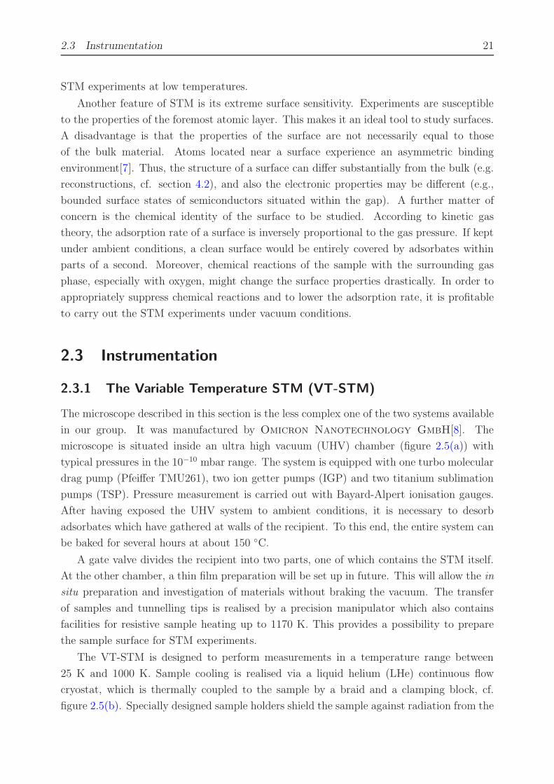
2.6 Slip/stick mode . . . . . . . . . . . . . . . . . . . . . . . . . . . . . . . . . . 22
2.5 The VT-STM . . . . . . . . . . . . . . . . . . . . . . . . . . . . . . . . . . . 23
2.7 The Cryogenic STM . . . . . . . . . . . . . . . . . . . . . . . . . . . . . . . 25
2.8 Sketch of the 3He cryostat . . . . . . . . . . . . . . . . . . . . . . . . . . . . 26
2.9 Vapour pressures of liquid 3He and 4He . . . . . . . . . . . . . . . . . . . . . 27
3.1 Pt/Ir vs. W tip . . . . . . . . . . . . . . . . . . . . . . . . . . . . . . . . . . 30
3.2 Electrochemical etching process . . . . . . . . . . . . . . . . . . . . . . . . . 32
3.3 W tip which had not been rinsed after etching . . . . . . . . . . . . . . . . . 34
3.4 H2 bubbles during etching . . . . . . . . . . . . . . . . . . . . . . . . . . . . 34
3.5 Potential at a metal surface . . . . . . . . . . . . . . . . . . . . . . . . . . . 36
3.6 Field emission current vs. voltage for two W tips . . . . . . . . . . . . . . . 37
3.7 Setup for field emission . . . . . . . . . . . . . . . . . . . . . . . . . . . . . . 37
3.8 Fowler-Nordheim plot . . . . . . . . . . . . . . . . . . . . . . . . . . . . . . . 38
3.9 SEM image of tip A in figures 3.6 and 3.8 . . . . . . . . . . . . . . . . . . . 39
3.10 Tip radii vs. field emission threshold voltage . . . . . . . . . . . . . . . . . . 40
3.11 Setup for electron heating . . . . . . . . . . . . . . . . . . . . . . . . . . . . 43
3.12 Tips annealed by electron bombardment . . . . . . . . . . . . . . . . . . . . 44
3.13 Influence of the annealing power on the tip sharpness . . . . . . . . . . . . . 45
3.14 Setup for Self-sputtering . . . . . . . . . . . . . . . . . . . . . . . . . . . . . 46
3.15 Voltage vs. time during self-sputtering . . . . . . . . . . . . . . . . . . . . . 47
3.16 Self-sputtered tips . . . . . . . . . . . . . . . . . . . . . . . . . . . . . . . . . 51
3.17 STM images before and after self-sputtering . . . . . . . . . . . . . . . . . . 52
3.18 Another sputter voltage curve . . . . . . . . . . . . . . . . . . . . . . . . . . 52
3.19 A tip which was accidentally blunted during self-sputtering . . . . . . . . . . 52
3.20 Stage for tip conditioning in the Cryogenic STM. . . . . . . . . . . . . . . . 55

8 LIST OF FIGURES
3.21 Stage for tip conditioning in the VT-STM. . . . . . . . . . . . . . . . . . . . 56
3.22 Block diagram of the power supply for field emission and self-sputtering (FESS) 57
4.1 Crystal structure of graphite . . . . . . . . . . . . . . . . . . . . . . . . . . . 59
4.2 Atomically resolved STM images of HOPG . . . . . . . . . . . . . . . . . . . 62
4.3 Moire patterns on HOPG . . . . . . . . . . . . . . . . . . . . . . . . . . . . 63
4.4 Differential conductance of HOPG . . . . . . . . . . . . . . . . . . . . . . . . 64
4.5 STM images of the Au(111) surface . . . . . . . . . . . . . . . . . . . . . . . 67
4.6 Model of the reconstructed Au(111) surface . . . . . . . . . . . . . . . . . . 68
4.7 Monoatomic step and herringbone pattern on Au(111) . . . . . . . . . . . . 68
4.8 STM images of an Au film on glass substrate . . . . . . . . . . . . . . . . . . 69
4.9 8 × 8 nm2 STM image of NbSe2, featuring a charge density wave . . . . . . 70
4.10 Temperature dependence of the critical fields for a type-II SC . . . . . . . . 71
4.11 Tunnelling spectra of NbSe2 at T = 385 mK, µ0H = 0.6 T . . . . . . . . . . 73
4.12 STS image of the vortex lattice in NbSe2 . . . . . . . . . . . . . . . . . . . . 74
A.1 Recipient and gas supplies of the Cryogenic STM . . . . . . . . . . . . . . . 80
A.2 Power supply for field emission and self-sputtering . . . . . . . . . . . . . . . 81

List of Symbols and Abbreviations
Symbols
A Angstrom unit; 1A= 0.1 nm= 10−10 m
α polarisability
a (as/av) lattice parametre (of a superlattice/vortex lattice)
b, c constants
B magniude of the magnetic flux density
d distance, gap width
δ(x) Dirac delta function
D diffusion constant
∆ superconducting energy gap
e charge of an electron, e = 1.602 × 10⁻¹⁹ C
E, ε; EF energy; Fermi energy
f(E, T ) Fermi function at energy E and temperature T
f(E, T ) = 1/[1 + exp(E−EF
kBT)]
F electric field strength, F = |F|Φ, Φeff work function, effective work function
ϕ angle
Γ pair breaking parametre
h, ~ Planck constant, ~ = h/2π
H magnitude of the magnetic field strength
I current
It tunnelling current
j magnitude of the current density
k wave number (chapter 2)
geometrical factor (chapter 3)
kB Boltzmann constant, kB = 1.381 × 10⁻²³ J/K
K force
κ decay length
m mass of the electron, m = 9.109 × 10⁻³¹ kg

10 LIST OF FIGURES
Mµν transition matrix element
µ0 vacuum permeability, µ0 = 4π × 10−7 N A−2
ω frequency
p pressure
p dipole moment, p = |p|P power
Ψ wave function
r radius of apex curvature of a tip
r = (x, y, z) spatial coordinates
ρ(E) (local) electronic density of states at energy E
t time
T temperature
Tc critical temperature of a superconductor
TP Peierls temperature of the CDW transition
T (tunnelling) transmission probability
θ angle
U , U0, Ueff potential
V voltage
Vth field emission threshold voltage; Ith = I(Vth)
Vgap gap voltage
W potential energy
ξ correction factor
LIST OF FIGURES 11
Abbreviations
AES Auger electron spectroscopy
AFM atomic force microscopy
CITS current imaging tunnelling spectroscopy
EDM electrical discharge machining
HOPG highly oriented pyrolytic graphite
HV high voltage
LEED low energy electron diffraction
LHe liquid helium
LN2 liquid nitrogen
MFM magnetic force microscopy
OVC outer vacuum chamber
SC superconductor, superconducting
STM scanning tunnelling microscope, or microscopy
STS scanning tunnelling spectroscopy
UHV ultrahigh vacuum
XPS X-ray photoelectron emission spectroscopy

1 Introduction
During the past century, considerable progress has been achieved in understanding the
fundamental phenomena in matter. A milestone was certainly the formulation of quantum
mechanics, which has paved the way towards a description of solids on an atomic level.
Advanced experimental techniques succeeded to reveal ever new information about the inner
structure of matter, which in turn stimulated the evolution of technologies in an unforeseen
manner. In order to push the frontiers of sciences to ever smaller scales, scientist had to cope
with the requirement to carry out experiments with increasingly high resolution. A rather
young but nontheless enormously successful approach to probe local properties of surfaces
with high spatial are the so-called scanning probe methods. A probe is proximated to a
surface to be investigated such that an interaction between probe and sample can take place.
Measurements of the local interaction strength at sequential locations can be assembled to
form an image. This concept can be applied to various interactions, for example van
der Waals interaction (atomic force microscopy), magnetic interaction (magnetic force
microscopy), or interaction with light (near-field scanning optical microscopy). The present
work deals with scanning tunnelling microscopy, which refers to the quantum phenomenon
of tunnelling. The distance between a conductive probe tip and a sample is reduced until
the electron wave functions of tip and sample surface have significant overlap, and electrons
can tunnel through the vacuum barrier. As the so-detected tunnelling current is strongly
distance-dependant, it can be used to map the morphology of the sample surface with a
resolution which goes far beyond the actual meaning of the term ”microscopy”. Besides
its unique spatial resolution, one strength of the STM is the possibility to perform local
electronic spectroscopy, and thereby gain valuable information about the sample’s electronic
properties. Invented in the early 1980’s, STM has evolved into a standard tool to investigate
the properties of surfaces and interfaces, with applications in various research fields besides
physics, such as material sciences, chemistry, or biology. A brief introduction to the method
of STM will be given in chapter 2 of this work, including theoretical aspects as well as their
technical application.
One important prerequisite for high quality STM is a good tunnelling tip. The properties
of the probe are reflected in the quality of the obtained data. The reliable preparation of
tunnelling tips is one of the most important, but also one of the most tricky experimental
14 1 Introduction
aspects of STM. The task of this work was it to optimise the preparation process of tungsten
tips for the use in ultrahigh vacuum STM. This toppic is addressed in detail in chapter 3 of
this thesis. The tungsten tips are produced by the commonly used electrochemical etching
procedure. For the use in STM, additional in-situ conditioning is necessary, specifically
to remove the dense oxide layer which inevitably evolves during the etching process, and
which may otherwise disturb the tunnelling experiment. Tip conditioning takes the main
stage within this work. Here, the following methods had been chosen: Direct resistive
annealing, annealing by electron bombardment, and self-sputtering with noble gas ions.
These methods seemed to be promising while being applicable in the existing STM systems
with a reasonable effort. The technical requirements had to be provided or adapted, if
already available. Specifically, stages for the in-situ conditioning were to be designed and
implemented into the respective vacuum chambers. Even though the solutions presented in
section 3.5 are adapted to the requirements of the STM’s of our group, the principle may well
be applicable to other systems, and it might even be used for other experimental techniques
which demand for sharp, clean conducting tips, as in other scanning probe methods.
The respective methods of tip conditioning had to be tested and optimised. To this end,
tips were characterised by means of electron microscopy and field emission experiments.
Naturally, the ultimate criterion for the quality of a tunnelling tip is to perform STM
experiments. Tunnelling microscopy and spectroscopy was carried out on various samples.
Selected STM data is presented in chapter 4, including for instance normal imaging and
superstructures on graphite, surface reconstruction on a gold single crystal surface, and
tunnellung spectroscopy in the mixed state of the type-II superconductor NbSe2.
The demand for ultrasharp and clean metal tips has been present already before the
invention of STM, for instance for the use in field ion microscopy. Throughout the years,
numerous methods for tip preparation and, specifically, for the conditioning of etched tung-
sten tips have been suggested and tried out (see chapter 3 and references therein). Also
the techniques used within this work have been known for some time, so reinventing the
wheel was not necessary. However, the work of other scientists can only to some extend
replace the gathering of own experience. Since there is probably no ”standard way” for
straightforward tip preparation, and the methods have to be adapted to the present tech-
nical circumstances and requirements, there is no way around finding one’s own way. In
addition, with a method as complex as STM, it is profitable to gain as much experience as
possible with the experimental setup. In case of STM, this naturally includes the handling
of the tunnelling tips. In this sense, the ”recipe for tip preparation” given in the Appendix
of this thesis is not claimed to be the ”ultimate way” to prepare tips, rather it may be seen
as guideline through one possible way, including the experiences which were made during
this work.

2 Basics of STM
This chapter addresses basic aspects of Scanning Tunnelling Microscopy (STM). Section 2.1
deals with quantum mechanical tunnelling in general, as far as it is necessary to understand
the concepts involved in this work. A more detailed theoretical treatment can be found for
instance in Ref. [1]. The working principle will be presented and discussed subsequently in
section 2.2. Finally, the two STM systems available in our group are briefly described in
section 2.3.
2.1 Quantum mechanical tunnelling
In quantum mechanics, a vacuum gap in between two conductive electrodes can be described
by a potential barrier. Let a barrier of constant height U0 be extended between 0 and d
on the z axis and consider a particle of energy E < U0 and mass m. The solutions of the
one-dimensional stationary single-particle Schrodinger equation then have the form
Ψ(z) =
b1eikz + c1e
−ikz, z < 0;
b2eκz + c2e
−κz, 0 ≤ z ≤ d;
b3eikz + c3e
−ikz, z > d
where k = 2m~2
√E and κ = 2m
~2
√U0 − E. In contrast to classical behaviour, there is a finite
probability for the particle to overcome the barrier. In order to obtain the transmission
probability T through the potential barrier, the current density operator
j =i~
2m(Ψ∇Ψ∗ − Ψ∗∇Ψ)
has to be evaluated for the incident and the transmitted waves, ji and jt, respectively. This
is,
T =jtji
= |c3|2 = · · · ≈ T0e−2κd (2.1)
Hence, the tunnelling current through the potential barrier decreases exponentially with the
barrier width. In a metal, an electron at Fermi energy EF experiences a potential barrier
of the height Φ = V0 −EF . Typical values for the work functions Φ of metals are 4− 5 eV,
hence κ is in the order of 1 A−1
. That is, the tunnelling current typically decreases by

16 2 Basics of STM
about one order of magnitude per 2 A width of the barrier. Even though this very simple
approach can certainly not explain STM in detail, it illustrates nicely its basic idea; that is,
to use tunnelling current as a sensitive measure for the distance between a sharp probe and
a sample in order to map the sample surface topography.
Already before the construction of the first STM in 1982[2], the phenomenon of tunnelling
had been subject to both experimental and theoretical investigations. One possible approach
was given by the transfer hamiltonian theory, as suggested by J. Bardeen in 1961[3]. In
most practical cases the tunnelling barrier is broad enough to assume weak coupling between
the two electrodes. In this case, each electrode can be treated separately, with a tunnelling
hamiltonian as perturbation. Then, the many-particle tunnelling current can be written to
first order as
I =2πe
~
∑
µν
|Mµν |2 [f(T,Eµ) − f(T,Eν)] δ(Eν + eV − Eµ) (2.2)
where f(T,E) is the Fermi function at temperature T , and V is the voltage applied between
the electrodes. The main obstacle is then to evaluate Mµν , the matrix element for the
transition of an electron in the state ψν in one electrode into a state ψµ in the other electrode.
For elastic tunnelling, Bardeen showed that
Mµν =~
2m
∫
dS(
ψ∗
µ∇ψν − ψν∇ψ∗
µ
)
. (2.3)
The integration surface lies in between the two electrodes.
In order to further evaluate Mµν for the case of STM, one has to take into account the
particular geometry of the setup. In an ideal STM, the probing electrode would only consist
of a single point. As shown by Tersoff and Hamann[4], equation (2.2) in this case reduces
to
I ∝∑
ν
|ψν(r)|2δ(Eν − EF ) ≡ ρs(r, EF ) (2.4)
where ψν(r) are wave functions in the sample electrode at the lateral position r of the probe,
and δ(x) is the Dirac delta function. Thus, the ideal STM would measure a tunnelling
current which is proportional to the sample’s local density of states (LDOS) at position of
the tunnelling tip. Relation (2.4) still holds for somewhat more realistic descriptions, as long
as the following constraints are fulfilled:
• The tip has an uniform density of states at the Fermi energy,
• the applied bias voltage is sufficiently small (≃ 10mV ),
• the temperature is low, and
• the tip wave functions are asymptotically spherical (s-wave tip).
2.1 Quantum mechanical tunnelling 17
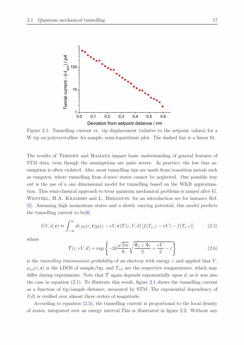
Figure 2.1: Tunnelling current vs. tip displacement (relative to the setpoint values) for a
W tip on polycrystalline Au sample, semi-logarithmic plot. The dashed line is a linear fit.
The results of Tersoff and Hamann impart basic understanding of general features of
STM data, even though the assumptions are quite severe. In practice, the low bias as-
sumption is often violated. Also, most tunnelling tips are made from transition metals such
as tungsten, where tunnelling from d-wave states cannot be neglected. One possible way
out is the use of a one dimensional model for tunnelling based on the WKB approxima-
tion. This semi-classical approach to treat quantum mechanical problems is named after G.
Wentzel, H.A. Kramers and L. Brillouin; for an introduction see for instance Ref.
[5]. Assuming high momentum states and a slowly varying potential, this model predicts
the tunnelling current to be[6]
I(V, d, r) ≈∫
∞
−∞
dε ρs(ε, r)ρt(ε− eV, r)T (ε, V, d) [f(Ts, ε− eV ) − f(Tt, ε)] (2.5)
where
T (ε, eV, d) = exp
−2d
√2m
~
√
Φs + Φt
2+eV
2− ε
(2.6)
is the tunnelling transmission probability of an electron with energy ε and applied bias V .
ρs/t(ε, r) is the LDOS of sample/tip, and Ts/t are the respective temperatures, which may
differ during experiments. Note that T again depends exponentially upon d, as it was also
the case in equation (2.1). To illustrate this result, figure 2.1 shows the tunnelling current
as a function of tip/sample distance, measured by STM. The exponential dependency of
I(d) is verified over almost three orders of magnitude.
According to equation (2.5), the tunnelling current is proportional to the local density
of states, integrated over an energy interval.This is illustrated in figure 2.2. Without any
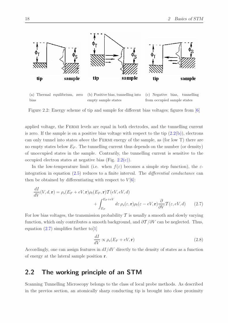
18 2 Basics of STM
(a) Thermal equilibrium, zero
bias
(b) Positive bias, tunnelling into
empty sample states
(c) Negative bias, tunnelling
from occupied sample states
Figure 2.2: Energy scheme of tip and sample for different bias voltages; figures from [6]
applied voltage, the Fermi levels are equal in both electrodes, and the tunnelling current
is zero. If the sample is on a positive bias voltage with respect to the tip (2.2(b)), electrons
can only tunnel into states above the Fermi energy of the sample, as (for low T) there are
no empty states below EF . The tunnelling current thus depends on the number (or density)
of unoccupied states in the sample. Contrarily, the tunnelling current is sensitive to the
occupied electron states at negative bias (Fig. 2.2(c)).
In the low-temperature limit (i.e. when f(ε) becomes a simple step function), the ε-
integration in equation (2.5) reduces to a finite interval. The differential conductance can
then be obtained by differentiating with respect to V [6]:
dI
dV(V, d, r) = ρs(EF + eV, r)ρt(EF , r)T (eV, eV, d)
+
∫ EF +eV
EF
dε ρs(ε, r)ρt(ε− eV, r)∂
∂VT (ε, eV, d) (2.7)
For low bias voltages, the transmission probability T is usually a smooth and slowly varying
function, which only contributes a smooth background, and ∂T /∂V can be neglected. Thus,
equation (2.7) simplifies further to[1]
dI
dV∝ ρs(EF + eV, r) (2.8)
Accordingly, one can assign features in dI/dV directly to the density of states as a function
of energy at the lateral sample position r.
2.2 The working principle of an STM
Scanning Tunnelling Microscopy belongs to the class of local probe methods. As described
in the previos section, an atomically sharp conducting tip is brought into close proximity
2.2 The working principle of an STM 19
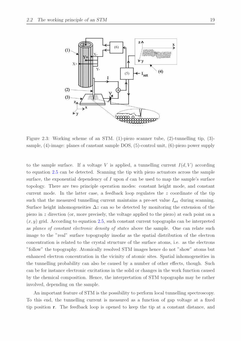
Figure 2.3: Working scheme of an STM. (1)-piezo scanner tube, (2)-tunnelling tip, (3)-
sample, (4)-image: planes of canstant sample DOS, (5)-control unit, (6)-piezo power supply
to the sample surface. If a voltage V is applied, a tunnelling current I(d, V ) according
to equation 2.5 can be detected. Scanning the tip with piezo actuators across the sample
surface, the exponential dependency of I upon d can be used to map the sample’s surface
topology. There are two principle operation modes: constant height mode, and constant
current mode. In the latter case, a feedback loop regulates the z coordinate of the tip
such that the measured tunnelling current maintains a pre-set value Iset during scanning.
Surface height inhomogeneities ∆z can so be detected by monitoring the extension of the
piezo in z direction (or, more precisely, the voltage applied to the piezo) at each point on a
(x, y) grid. According to equation 2.5, such constant current topographs can be interpreted
as planes of constant electronic density of states above the sample. One can relate such
image to the ”real” surface topography insofar as the spatial distribution of the electron
concentration is related to the crystal structure of the surface atoms, i.e. as the electrons
”follow” the topography. Atomically resolved STM images hence do not ”show” atoms but
enhanced electron concentration in the vicinity of atomic sites. Spatial inhomogeneities in
the tunnelling probability can also be caused by a number of other effects, though. Such
can be for instance electronic excitations in the solid or changes in the work function caused
by the chemical composition. Hence, the interpretation of STM topographs may be rather
involved, depending on the sample.
An important feature of STM is the possibility to perform local tunnelling spectroscopy.
To this end, the tunnelling current is measured as a function of gap voltage at a fixed
tip position r. The feedback loop is opened to keep the tip at a constant distance, and
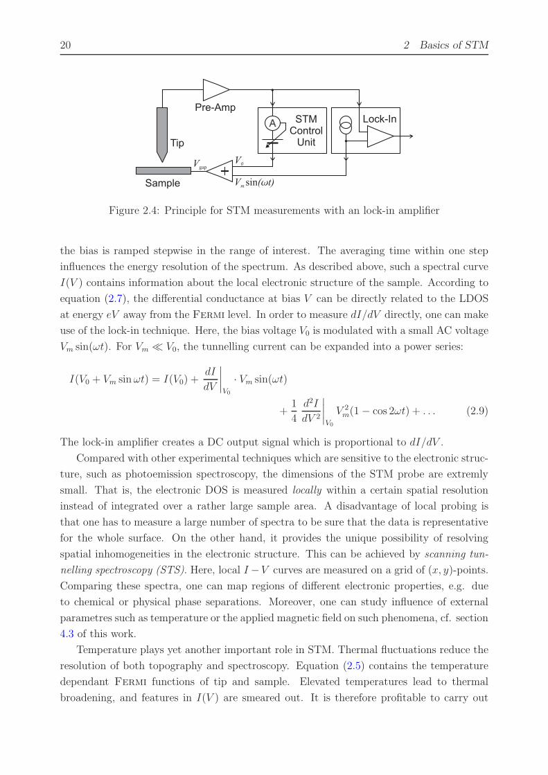
20 2 Basics of STM
Figure 2.4: Principle for STM measurements with an lock-in amplifier
the bias is ramped stepwise in the range of interest. The averaging time within one step
influences the energy resolution of the spectrum. As described above, such a spectral curve
I(V ) contains information about the local electronic structure of the sample. According to
equation (2.7), the differential conductance at bias V can be directly related to the LDOS
at energy eV away from the Fermi level. In order to measure dI/dV directly, one can make
use of the lock-in technique. Here, the bias voltage V0 is modulated with a small AC voltage
Vm sin(ωt). For Vm ≪ V0, the tunnelling current can be expanded into a power series:
I(V0 + Vm sinωt) = I(V0) +dI
dV
∣
∣
∣
∣
V0
· Vm sin(ωt)
+1
4
d2I
dV 2
∣
∣
∣
∣
V0
V 2m(1 − cos 2ωt) + . . . (2.9)
The lock-in amplifier creates a DC output signal which is proportional to dI/dV .
Compared with other experimental techniques which are sensitive to the electronic struc-
ture, such as photoemission spectroscopy, the dimensions of the STM probe are extremly
small. That is, the electronic DOS is measured locally within a certain spatial resolution
instead of integrated over a rather large sample area. A disadvantage of local probing is
that one has to measure a large number of spectra to be sure that the data is representative
for the whole surface. On the other hand, it provides the unique possibility of resolving
spatial inhomogeneities in the electronic structure. This can be achieved by scanning tun-
nelling spectroscopy (STS). Here, local I−V curves are measured on a grid of (x, y)-points.
Comparing these spectra, one can map regions of different electronic properties, e.g. due
to chemical or physical phase separations. Moreover, one can study influence of external
parametres such as temperature or the applied magnetic field on such phenomena, cf. section
4.3 of this work.
Temperature plays yet another important role in STM. Thermal fluctuations reduce the
resolution of both topography and spectroscopy. Equation (2.5) contains the temperature
dependant Fermi functions of tip and sample. Elevated temperatures lead to thermal
broadening, and features in I(V ) are smeared out. It is therefore profitable to carry out
2.3 Instrumentation 21
STM experiments at low temperatures.
Another feature of STM is its extreme surface sensitivity. Experiments are susceptible
to the properties of the foremost atomic layer. This makes it an ideal tool to study surfaces.
A disadvantage is that the properties of the surface are not necessarily equal to those
of the bulk material. Atoms located near a surface experience an asymmetric binding
environment[7]. Thus, the structure of a surface can differ substantially from the bulk (e.g.
reconstructions, cf. section 4.2), and also the electronic properties may be different (e.g.,
bounded surface states of semiconductors situated within the gap). A further matter of
concern is the chemical identity of the surface to be studied. According to kinetic gas
theory, the adsorption rate of a surface is inversely proportional to the gas pressure. If kept
under ambient conditions, a clean surface would be entirely covered by adsorbates within
parts of a second. Moreover, chemical reactions of the sample with the surrounding gas
phase, especially with oxygen, might change the surface properties drastically. In order to
appropriately suppress chemical reactions and to lower the adsorption rate, it is profitable
to carry out the STM experiments under vacuum conditions.
2.3 Instrumentation
2.3.1 The Variable Temperature STM (VT-STM)
The microscope described in this section is the less complex one of the two systems available
in our group. It was manufactured by Omicron Nanotechnology GmbH[8]. The
microscope is situated inside an ultra high vacuum (UHV) chamber (figure 2.5(a)) with
typical pressures in the 10−10 mbar range. The system is equipped with one turbo molecular
drag pump (Pfeiffer TMU261), two ion getter pumps (IGP) and two titanium sublimation
pumps (TSP). Pressure measurement is carried out with Bayard-Alpert ionisation gauges.
After having exposed the UHV system to ambient conditions, it is necessary to desorb
adsorbates which have gathered at walls of the recipient. To this end, the entire system can
be baked for several hours at about 150 C.
A gate valve divides the recipient into two parts, one of which contains the STM itself.
At the other chamber, a thin film preparation will be set up in future. This will allow the in
situ preparation and investigation of materials without braking the vacuum. The transfer
of samples and tunnelling tips is realised by a precision manipulator which also contains
facilities for resistive sample heating up to 1170 K. This provides a possibility to prepare
the sample surface for STM experiments.
The VT-STM is designed to perform measurements in a temperature range between
25 K and 1000 K. Sample cooling is realised via a liquid helium (LHe) continuous flow
cryostat, which is thermally coupled to the sample by a braid and a clamping block, cf.
figure 2.5(b). Specially designed sample holders shield the sample against radiation from the
22 2 Basics of STM
environment. Elevated sample temperatures are reached by radiative heating with a PBN
(pyrolytic boron nitride) heating element. Note that only the sample itself is thermalised,
while the surrounding STM components remain at room temperature. This allows for a fast
thermalisation and a high flexibility of conditions. However, the high temperature at the tip
lowers the resolution (the Fermi function at the tip becomes very broad, cf. equation 2.5),
and the large temperature gradient between tip and sample might cause undesired effects
due to thermal drift.
A crucial prerequisite for achieving high resolution and low-noise STM data is isolation
against external vibrations. The latter can easily interfere with data features such as atomic
corrugations. For this purpose, the VT-STM is mounted on a platform which is spring-
suspended inside the UHV chamber (eigenfrequency ≈ 2 Hz). Permanent magnets and
copper plates are mounted to render a nearly non-periodic eddy current damping.
“slip”~2µs
“stick”~1ms
“stick”
V
t
Figure 2.6: Schematic of
the voltage supplied to the
coarse piezo during one step
As mentioned in the previous section, the relative move-
ments of tip and sample are carried out by piezo ceramics.
The VT-STM uses a tube scanner, which is visible in figure
2.5(b) (cf. also the illustration in figure 2.3). The tube consists
of multiple electrodes to facilitate lateral as well as longitudi-
nal contraction. The maximum travel is limited to 12×12 µm2
laterally and 1.5 µm in z direction . Additional piezo motors
are implemented for coarse positioning in x and y direction and
movement in z direction. These coarse piezos are operated in
so-called slip/stick mode. Sliders are magnetically coupled to
shear piezos. If a sawtooth voltage as in figure 2.6 is applied,
the sliders are transported by the piezos during the slow piezo
movement (”stick”), and slip during the fast movement due to
their inert mass. The result is a relative movement of slider and piezo. In this way, relatively
large translations can be carried out. Approaching tip and sample to tunnelling distance
is done automatically as follows. The scanner is extracted in z direction until a tunnelling
current is flowing. If at maximum extraction no current is yet detected, the scanner is
retracted, and the coarse piezo steps forwards by less than the maximum extraction of the
scanner. This cycle is repeated until the tip is within tunnelling distance to the sample. The
tip is mounted upwards in a tip holder which itself is held magnetically on the scanner. The
gap voltage is supplied to the tip whereas the sample holder is connected to ground. The
measured output signals are passed through a preamplifier (Omicron SPM Pre 4) outside
the STM into the control unit (Omicron Matrix SPM-CU).
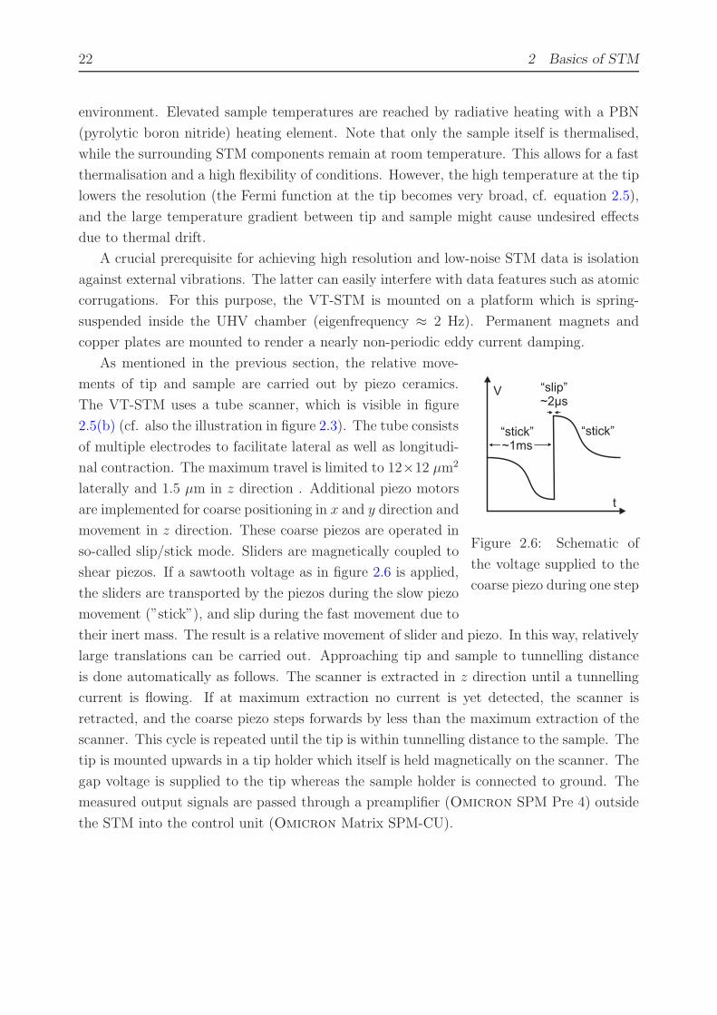
2.3 Instrumentation 23
(a) The UHV recipient with MBE chamber (1) and STM cham-
ber (2), separated by a gate valve (3); transfer manipulator (4),
cluster flange (5), and CCD camera for tip positioning (6).
(b) The STM: scanner tube (1), tip holder (2) with a tip pointing
upwards, sample plate (3) (cooling version), and clamping block
for thermal coupling to the cryostat (4)
Figure 2.5: The VT-STM
24 2 Basics of STM
2.3.2 The Cryogenic STM
Compared to the former, the system described in this section is technically far more complex
because it combines the following requirements:
• UHV conditions
• a temperature range down to 350 mK
• a magnetic field of µ0H = 12 T in z direction
• high stability due to sophisticated vibration isolation
• facilities for sample preparation and analysis
The system was manufactured by Omicron Nanotechnology GmbH as a prototype.
UHV system
The apparatus has been designed as a two chamber UHV system (figure 2.7). The prepa-
ration chamber includes facilities for the in situ preparation and characterisation of sample
surfaces: As in the VT-STM, samples can be heated on the transfer manipulator. An argon
sputter gun and a cleaving tool provide additional possibilities to prepare clean and smooth
surfaces. An electron source or a X-ray source can be used in combination with an energy
analyser to characterise samples by X-ray photoemission electron spectroscopy (XPS) or
Auger electron spectroscopy (AES), respectively. Low energy electron diffraction (LEED)
can reveal information about the atomic structure and symmetry of surfaces. The STM
chamber is separated by a gate valve and extends to the innermost part of the cryostat.
The 3He cryostat
The system is equipped with a single shot 3He cryostat manufactured by Oxford Ltd.[9]
Figure 2.8 sketches the cryostat setup. For thermal shielding against the enviroment, reser-
voirs for liquid nitrogen (LN2) and LHe are arranged concentrically around the cold inner
part. The outer vacuum chamber (OVC) thermally decouples the respective containers. The
so-called UHV sock separates the OVC from the inner UHV chamber which contains the
STM. The main function of this additional double-walled vacuum specimen is it to facilitate
the baking of the cryostat while the STM chamber remains evacuated. To this end, hot dry
air is drawn through the UHV sock such that the inner part of the cryostat is radiatively
heated. During normal operation, a flow of 4He gas cools the innermost wall of the UHV
sock.
The heart of the cryostat is the UHV compatible Heliox insert. The setup is sketched in
figure 2.8b). For cooling, the 1K pot is partially filled with LHe through a capillary from
2.3 Instrumentation 25
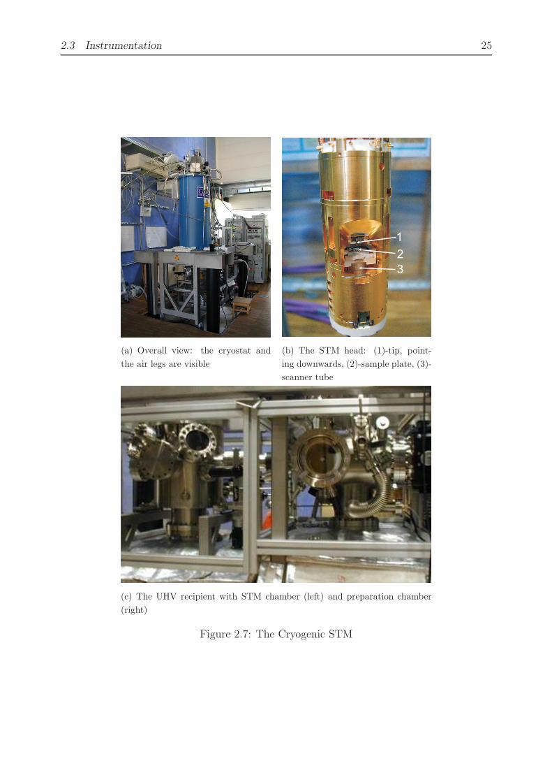
(a) Overall view: the cryostat and
the air legs are visible
(b) The STM head: (1)-tip, point-
ing downwards, (2)-sample plate, (3)-
scanner tube
(c) The UHV recipient with STM chamber (left) and preparation chamber
(right)
Figure 2.7: The Cryogenic STM
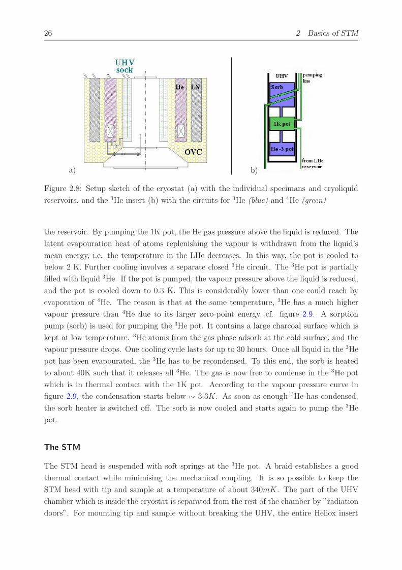
26 2 Basics of STM
a) b)
Figure 2.8: Setup sketch of the cryostat (a) with the individual specimans and cryoliquid
reservoirs, and the 3He insert (b) with the circuits for 3He (blue) and 4He (green)
the reservoir. By pumping the 1K pot, the He gas pressure above the liquid is reduced. The
latent evapouration heat of atoms replenishing the vapour is withdrawn from the liquid’s
mean energy, i.e. the temperature in the LHe decreases. In this way, the pot is cooled to
below 2 K. Further cooling involves a separate closed 3He circuit. The 3He pot is partially
filled with liquid 3He. If the pot is pumped, the vapour pressure above the liquid is reduced,
and the pot is cooled down to 0.3 K. This is considerably lower than one could reach by
evaporation of 4He. The reason is that at the same temperature, 3He has a much higher
vapour pressure than 4He due to its larger zero-point energy, cf. figure 2.9. A sorption
pump (sorb) is used for pumping the 3He pot. It contains a large charcoal surface which is
kept at low temperature. 3He atoms from the gas phase adsorb at the cold surface, and the
vapour pressure drops. One cooling cycle lasts for up to 30 hours. Once all liquid in the 3He
pot has been evapourated, the 3He has to be recondensed. To this end, the sorb is heated
to about 40K such that it releases all 3He. The gas is now free to condense in the 3He pot
which is in thermal contact with the 1K pot. According to the vapour pressure curve in
figure 2.9, the condensation starts below ∼ 3.3K. As soon as enough 3He has condensed,
the sorb heater is switched off. The sorb is now cooled and starts again to pump the 3He
pot.
The STM
The STM head is suspended with soft springs at the 3He pot. A braid establishes a good
thermal contact while minimising the mechanical coupling. It is so possible to keep the
STM head with tip and sample at a temperature of about 340mK. The part of the UHV
chamber which is inside the cryostat is separated from the rest of the chamber by ”radiation
doors”. For mounting tip and sample without breaking the UHV, the entire Heliox insert

2.3 Instrumentation 27
Figure 2.9: Vapour pressures of liquid 3He and 4He. Figure taken from [10]
can be lowered out of the cryostat into a part of the chamber where the head is accessible
with a wobble stick. The STM head is surrounded by a radiation shield, consisting of two
tubes. The inner tube can be rotated against the outer one to access the head through
openings.
To prevent mechanical instability, the design of the STM head itself is made very compact
and rigid. Therefore, no AFM/MFM option was included. Moreover, there is only one lateral
degree of freedom in sample course movement. Tip positioning has to be carried out when
the insert is lowered out of the cryostat. When inside the cryostat, the STM is not visible
from outside, and one has to work ”blindly”. In contrast to the VT-STM, the gap voltage
is here applied to the sample, whereas the tip is connected to ground.
A superconducting magnet is situated in the LHe reservoir of the cryostat. In its op-
erating position, the STM head is positioned in the centre of the magnetic field. The
maximum field at the sample position is µ0H = 12 T perpendicular to the sample surface.
In this way, field induced variations of the sample’s electronic structure can be studied.
Electronic phase separations can be directly observed by STS, e.g. vortex lattices in type-II
superconductors[11].
Vibration isolation
One reason for the considerable effort in cryotechnique is that various phenomena only
occur at low temperatures, such as superconductivity. Another, equally important fact is
that the resolution of STM decreases at higher temperatures. This is particularly distructive
for the energy resolution of STS: The broadening of the Fermi distribution smears out the
spectroscopic features, cf. equation (2.5). The requirement of high resolution demands for
an involved isolation against external vibrations, too. Because of the strong magnet, an
eddy current damping as in the VT-STM, cf. the section 2.3.1 is not practicable here. The
28 2 Basics of STM
vibration isolation of this STM system consists of various features:
• The basement underneath the system is decoupled from the surrounding flour of the
building.
• The apparatus rests on four pneumatic legs with an active vibration damping.
• All pumping lines pass a massive concrete pit.
• The STM head is suspended on springs inside the chamber. Together with the high
mass of the head, the springs have a low eigenfrequency. Thermal contact is realised
with a braid instead of a solid connection.
The spring suspension of the STM head is a very effective decoupling. However, it may
also become a source of trouble in connection with the limited space available inside the
cryostat. The diameter of the STM head is 46 mm, whereas the bore of the inner radiation
shield is two inched wide. That is, there is a spacing of only 2 mm between the head and the
shielding. Because of the length of the suspension springs, even tiny lateral forces exerted on
the head may be enough to make the head touching the radiation shield. This mechanical
and thermal coupling may then in turn distort the measurements and the thermalisation
at lowest temperatures. Such tiny forces might for instance originate in small magnetic
moments. As calculations show, already tiny magnetic inhomogeneities may be sufficient in
connection with a radially inhomogeneous magnetic field, such as the field induced by the
magnet in our STM. As a consequence, one has to be extremely careful with the choice of
materials used for the construction. As an example, contacts and screws for the use in UHV
are often gold coated to prevent oxidation. The deposition of gold onto a metal surface
requires an underlayer because gold would not easily stick to the surface. One suitable
and frequently used material for this purpose is nickel. In our case the use of nickel would
lead into trouble, since nickel is ferromagnetic. It would be preferable to choose chromium
instead. A further issue of concern is the material of the head itself. Originally, the head
was intended to be made from titanium. But because of the magnetic moment of titanium,
the latter had to be replaced by a bronce with a very low magnetic susceptibility.
3 The preparation of tunnelling tips
One important prerequisite for obtaining high quality STM and, specifically, spectroscopic
data is a good tunnelling tip. As for any technique, one cannot expect the results to be better
than the probe allows. The reproducible preparation of tunnelling tips is therefore one of the
experimental key aspects of STM. In order to define the requirements to such preparation
process, section 3.1 focuses on the role of the tip in STM. The influence of the tip material, of
contaminants at the tip surface, and of the tip shape on STM experiments will be discussed
in this section. Therein, it will also be explained why we are mainly interested in the use
of tungsten (W) tips. A standard procedure to prepare such tips is electrochemical etching.
The method will be described in section 3.2, along with some remarks on how the process
can be optimised to improve the success rate of as-etched tips in STM. Equally important
is additional treatment of the tips after etching. A number of conditioning methods have
been studied in this work. In order to judge the efficiency of such methods and to optimise
them, means of tip characterisation were necessary, which will be discussed in section 3.3.
The conditioning methods will be presented and compared in section 3.4. Finally, section
3.5 deals with the technical realisation of in-situ tip conditioning in our STM systems.
3.1 The role of the tunnelling tip
It is intuitively clear for any measurement technique that the properties of the probe may
have major impact on the quality of the obtained data. It shall be discussed which role the
tunnelling tip plays in scanning tunnelling microscopy and spectroscopy, and what are thus
the requirements to any tip preparation in order to get optimum results.
The two attributes relevant for the performance of a tunnelling tip are its shape and its
chemical composition[12]. The latter involves two issues: the material which the tip is made
of, and contaminations present on the tip surface. Contaminants can lead to severe distortion
of the STM experiment. Insulating layers covering the tip apex such as metal oxides (e.g.
oxides of the tip material itself) act as additional tunnelling barriers which the electrons
have to overcome. The resolution would be reduced because it would be more difficult to
stabilise the tunnelling current, and for small gap voltages the tip could even crash and
cause damage to sample and tip[13]. Even more disturbing are such contamination layers

30 3 The preparation of tunnelling tips
Figure 3.1: Left: Pt80/Ir20 tip cut from 0.25mm wire with some pincers; right: W tip,
etched from 0.375mm polycrystalline wire
for spectroscopic experiments, as they might lead to additional spectral features superposed
to the measurement data. Small features in the sample’s electronic structure close to the
Fermi level may not even be resolvable any more. In the presence of the electric field
between tip and sample, adsorbates on the tip surface may migrate towards the tip apex
([14], cf. section 3.4.3 of this work). This might completely change the properties of the tip
and render the data useless.
The tip material itself also influences the properties of the obtained STM data[12].
According to equation (2.5), the tunnelling current depends not only on the electronic DOS
of the sample, but also on that of the tip. A variety of materials has been used for the
manufacture of tunnelling tips throughout the history of STM[12]. For most applications,
”normal” metallic tips are best suitable. However, some experimental tasks call for more
”exotic” materials. For example, superconducting tips have been fabricated from lead,
aluminium[15] or niobium[16]. Spin polarised STM can be performed with ferromagnetic
or antiferromagnetic probes, as for example with tips made from Ni[17], CrO2[18] or with
tungsten tips covered by a thin layer of iron or chromium[19].
One commonly used tip material is platinum iridium (Pt-Ir). This alloy is particularly
suitable for the use under ambient conditions because Pt is relatively inert to oxidation. A
fraction of Ir is convenient to make the tip harder. Another advantage is the uncomplicated
preparation. With some experience, cutting a piece of Pt-Ir wire with a punch or a pair
of scissors (see figure 3.1) gives sufficiently sharp tips to achieve atomic resolution. The
success rate is rather low, though. Additionally, Pt-Ir tips are mechanically unstable and
therefore only of limited use for spectroscopic measurements. Tungsten is a widely used
element for STM tips, and it also fits best to our experimental purposes: Since we intend to
work exclusively under UHV conditions, there is no risk of oxidation of clean tips once they
are inside the vacuum chamber. Tungsten is suitable for use at low temperatures, since it
becomes superconducting only below 10 mK. Above this temperature, the transition metal
3.1 The role of the tunnelling tip 31
has a high and comparatively smooth DOS at the Fermi energy[20], so that tungsten
is feasible for spectroscopic measurements. Last not least, tungsten is a very hard and
mechanically stable material. For those reasons, the preparation of tungsten STM tips is in
the main focus of this work.
The preparation of tips from W single crystals has been reported (see for instance Refs.
[21], [22]). Within this work, tips were made from polycrystalline W wire. Such wire is
easier to obtain (and therefore much cheaper) and easier to handle than pieces of single
crystals. A carefully prepared polycrystalline W tips can end with small single-crystalline
grains which are few nanometres in size[23]. High resolution STM data can be achieved
even though the crystallographic orientation of those small grains is at angles with the tip
axis. We used 99.95% pure polycrystalline tungsten wire with a diameter of 0.375 mm.[24]
On a macroscopic scale, a tunnelling tip has to be stable against mechanical vibra-
tions, as the latter might disturb data acquisition. Long and thin tips are generally less
favourable than ones which have a rather short and thick shank and taper rapidly towards
the apex. Such tips have higher eigenfrequencies and are generally more stable [12]. Far
more important than the macroscopic shape of a tunnelling tip, though, is its structure on
an atomic scale. One of the outstanding features of scanning tunnelling microscopy is its
unique spatial resolution. If carried out under adequate conditions, one can resolve features
which are on the length scale of interatomic distances in solids. One limiting factor for
the spatial resolution is the dimension of the probe. Due to the exponential dependency of
the tunnelling current upon the distance (cf. figure 2.1), essentially only electrons at the
few foremost atoms of the tip contribute to tunnelling. As an ideal tip, one could think
of a tip terminating in one single atom. The controlled building of such a tip is possible,
but it is rather involved[21, 25]. However, it is possible to achieve atomic resolution with
tips which microscopically have finite radii of apex curvature of about 10 to 20 nm[23, 13].
Tunnelling then occurs at those few atoms which happen to ”stick out farthest” from the
apex[12]. That is, the sharpest tips do not necessarily yield the highest resolution. But the
sharper the tip is on a microscopic scale, the higher is the possibility that the tunnelling
current flows only through one of such ”minitips” consisting of just few atoms. If tunnelling
occurred at two or more spots at the tip apex, the resolution would be reduced, and multiple
images of sample features might be superposed in the resulting one[12].
Even if tunnelling took place only at one spot of the tip apex, the atomic arrangement
could easily change during scanning which might then cause discontinuities in the data.
This is particularly severe for spectroscopic measurements. High energy resolution can only
be achieved with appropriately long averaging times. Consequently, STS measurements
can easily take several hours. The atomic configuration of the tip should thus be stable
throughout such time intervals.
In conclusion, the aim of any tip preparation or conditioning is it to routinely obtain
tips which are
32 3 The preparation of tunnelling tips
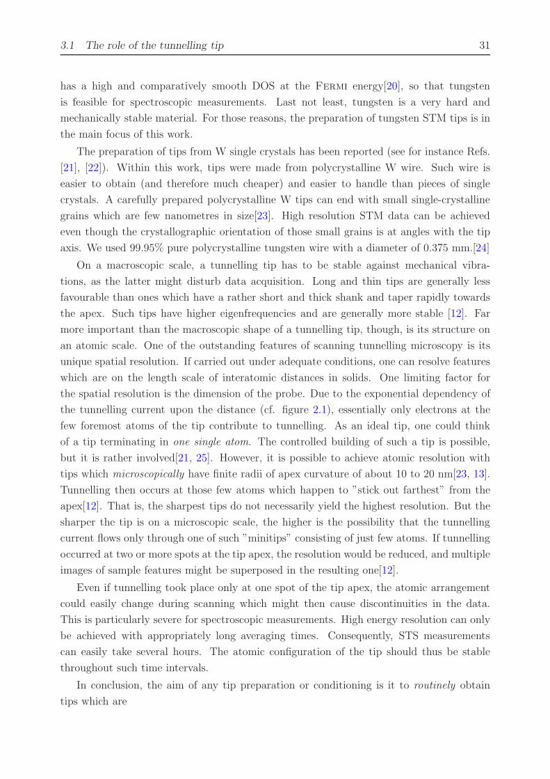
Figure 3.2: Illustration of the electrochemical etching process. b) to e) show the necking
close to the meniscus, the flow of WO2−4 ions (arrows) and the formation of a dense WO3
layer around the wire. In f), the lower part eventually drops off. Figure taken from [29]
• sharp enough to achieve the spatial resolution required
• mechanically stable, and
• free of any disturbing contamination.
In the following section, some aspects of the manufacture of tungsten tips will be outlined. It
shall be noted that this is not to be a complete presentation of all possible or conceivable ways
to produce high quality tips. It shall rather show the procedures as they were investigated
within the scope of this work.
3.2 Electrochemical etching
A generally applied method to produce sharp tungsten tips is electrochemical etching ([26],
[27], [28]). A piece of polycrystalline tungsten wire is mounted to a holder and immersed into
caustic soda solution (NaOH). The immersion depth can be varied. A ring-shaped stainless
steel wire is situated concentrically around the W anode and serves as counter electrode. If
a voltage is applied between the two electrodes, the following reaction takes place:
W(s) + 8OH− → WO2−4 + 4H2O + 6e− (anode)
6H2O + 6e− → 3H2(g) + 6OH− (cathode)
W(s) + 2H2O + 2OH− → WO2−4 + 3H2(g)
(3.1)
At the interface of electrolyte and air, solid tungsten is oxidised to tungstate anions (WO2−4 )
which are soluble in water. At the cathode, water molecules are reduced to hydroxide ions
(OH−) and hydrogen gas. The latter is visible as gas bubbles in the etchant. Figure 3.2
illustrates the evolution of the etching process. The dissolution of tungsten causes the
formation of a neck on the wire. The inhomogeneous etching rate leading to the neck has
two reasons[27]: Firstly, the surface tension of the etching liquid causes the formation of a
meniscus around the W electrode. The etching rate at the top of the meniscus is lower than
3.2 Electrochemical etching 33
further down due to a concentration gradient caused by diffusion of OH− towards the anode.
Secondly, the WO2−4 ions evolving during etching flow towards the lower end of the anode
wire and generate a dense viscous layer which prevents the lower part from being etched. As
a result of both effects, the etching rate is largest somewhat below the surface of the etchant.
As the reaction (3.1) proceeds, the neck becomes thinner and thinner until it finally breaks,
and the lower part drops off. The resulting tip has a radius of apex curvature in the order
of about 20 to 50nm. To our experience, a too quick etching frequently causes irregularly
shaped tips, whereas a too long duration of the process results in rather long and thin tips.
Sharp and regularly shaped tips can be obtained with applied voltages of 8-9 V for 3 M
NaOH solution. For higher (lower) molarities, the voltage has to be decreased (increased)
anti-proportionally. For the wire in use, initial immersion depths of 1.5 to 2.0 mm gave
good results. If the wire were dipped too deeply into the etchant, the neck would break too
early due to the higher mass of the part below the neck, resulting in less sharp tips. For too
small immersion depths, we frequently observed irregularly long and thin tips which were
often bended. An explanation could be that the head-and-neck shape is degenerated, and
no drop-off can occur.
The etching process has to be terminated immediately after the drop-off in order to
prevent the tip from being blunted by further etching. To this end, we monitored the current
flowing between the electrodes at a fixed etching voltage. During etching, the area of the W
surface which is immersed into the electrolyte is reduced, thus the current decreases nearly
linearly with time[26]. The breaking of the neck can be detected as a sudden decrease of the
current. In our case, the etching power supply (Omicron Nanotechnology GmbH[8])
automatically terminates the etching process as soon as the current drops below a pre-set
threshold value. Alternatively, the jump can be detected by monitoring changes in the
differential current. After drop-off, the tip is taken out of the solution and carefully rinsed
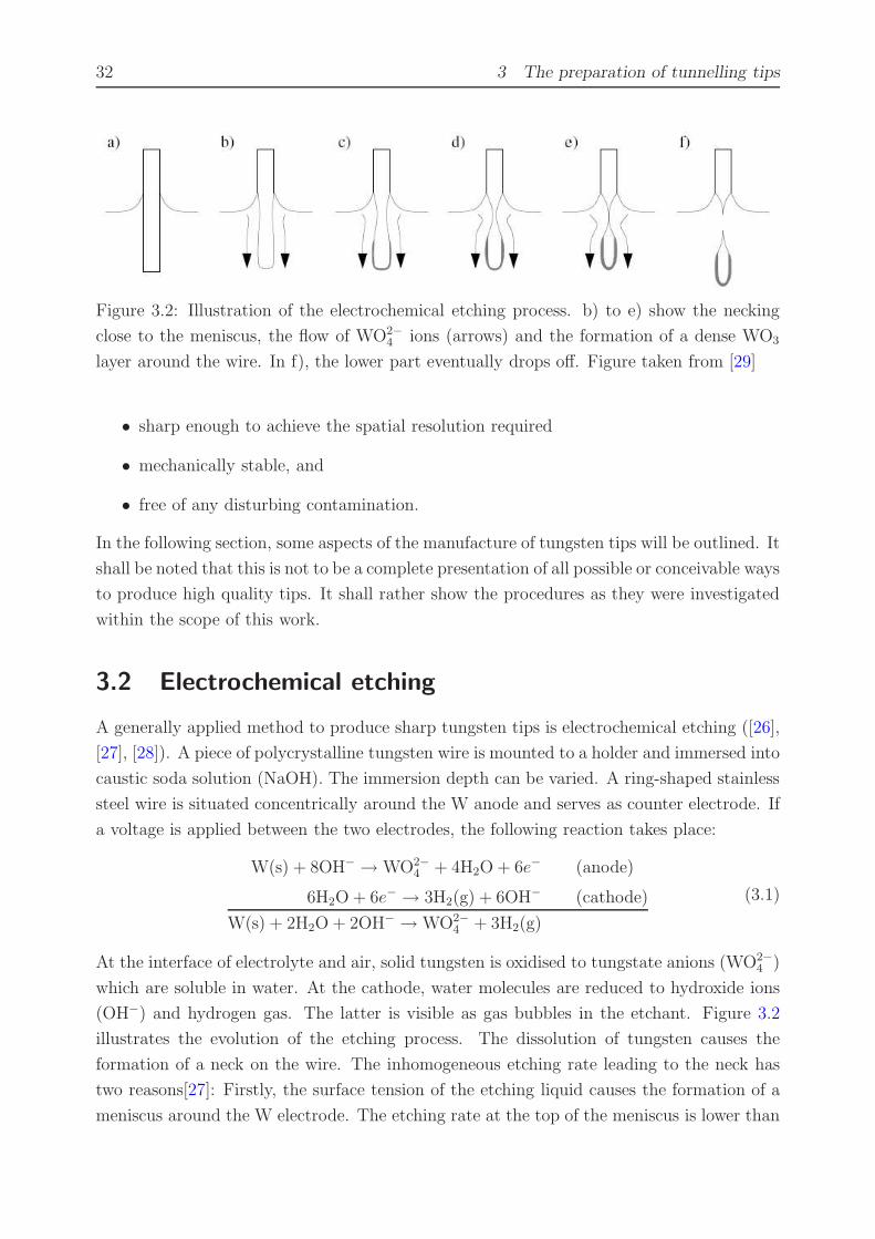
in de-ionised water, in order to remove remainders of the etchant. Figure 3.3 shows a tip
which had not been cleaned after etching. The tip is almost completely covered by sodium
hydroxide crystals which may severely disturb STM experiments. After being dried with
clean nitrogenic gas, tips are ready to be loaded into the UHV system.
The as-etched tips are rather fragile and have to be handled carefully. During our
experiments, a number of procedures turned out to be useful to optimise the tip quality,
or to increase their success rate. As a result of its production process, the surface of the
polycrystalline tungsten wire contains residual carbon and has an irregular and grooved
shaped. At the beginning of the etching, we could observe fibres coming off the wire. Those
fibres remained on the surface of the etchant and frequently stuck to the readily etched tip
when it was pulled out of the solution. The tips were then often visibly bent and could not
be used further. A simple solution to this problem is to shortly pre-etch a larger part of the
wire than required for the actual etching step in a separate NaOH solution (a more detailed
description is given in the Appendix).
34 3 The preparation of tunnelling tips
Figure 3.3: A tungsten tip which had not been rinsed after etching
As described, the NaOH surface forms a meniscus around the tungsten wire during
etching. As the neck in the wire deepens, the meniscus can drop to a lower position, often
leading to the formation of a second neck below the first one. This may result in oddly
shaped, mechanically unstable tips. It is therefore profitable to observe the etching process
through an optical microscope and to lower the tip by about 0.1 mm after a few minutes in
order to reduce the surface tension. The reduced height of the meniscus is also profitable
for the tip shape, since the aspect ratio of the etched tip is mainly determined by the shape
of the meniscus, and a lower meniscus results in shorter tips[27]. The observation of the
process may cause additional vibrations which might disturb the etching, especially in an
advanced state when the neck is already thin. For this reason we situated our etching tool
on top of a heavy stone block based on rubber feet. Moreover, we put a plexiglass shield
to protect the NaOH surface from air flow. In this way, the vibrations of the lower part of
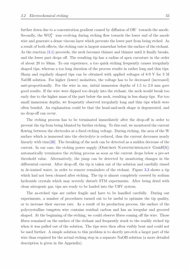
the etched wire could be reduced visibly. Another undesired effect results from the H2 gas
evolving at the cathode according to the reaction (3.1). Due to the inhomogeneous electric
field between the concentric electrodes, the gas bubbles migrate from the cathode towards
the tungsten anode where they frequently disturb the etching process. We found that the
amount of gas bubbles which actually reach the anode depends on the immersion depth of
Figure 3.4: Bubbles of H2 gas evolving at the cathode can migrate towards the W anode and
disturb the etching (a). If the cathode is only touching the surface of the etchant, almost
no gas bubbles can reach the anode (b)
3.3 Means of tip characterisation 35
the counter electrode into the NaOH solution. This is illustrated in figure 3.4 If the cathode
is mounted in such a way that it is just touching the surface of the etchant, almost no gas
bubbles are visible at the anode.
A major disadvantage of electrochemical etching is that tips prepared in this way are
covered by a dense oxide layer. Hence, additional treatment is necessary after etching. This
toppic will be addressed in detail in section 3.4. The rate of tips which, after etching, could
be used for any further treatment was about 50%. If the tips had been stored for one day or
longer in air, the rate would have been worse, probably due to proceeding oxidation. Storing
the tips in ethanol seemed profitable, though. Firstly, the tips did not oxidise any further,
and the fraction of useable tips was increased. And secondly, any organic contaminants
were removed from the tip at the same time.
3.3 Means of tip characterisation
In order to study the efficiency of tip preparation methods, it is necessary to characterise
tips in a reproducible manner. The ultimate way to test the quality of a STM tip would
be to perform tunnelling experiments with well-known reference samples. With a blunt
or strongly contaminated tip, it would not be possible to achive stable atomic resolution.
Multiple tips cause anisotropic or multiple imaging of sample features. Spectroscopic mea-
surements can provide information on the presence of additional non-metallic layers on the
tip surface. However, STM measurements are generally quite time consuming, and a differ-
entiated characterisation of the tim by STM is not easily possible because of the variety of
parametres which influence the STM data.
A more direct way to determine the tip morphology is to visualise them. With an optical
microscope one can see whether a tip is bent or irregularly shaped only on a macroscopic
scale, which anyway is often useful. By means of scanning electron microscopy (SEM), the
shape can be probed in the sub-micrometre range. The actual atomic arrangement in not
accessible, though. SEM experiments are time consuming as well, and they have to be
carried out ex situ. Therefore, it is convenient to have a means to check quickly on tip
sharpness and cleanliness already before and during the conditioning process. In this way,
one can quantify the impact a certain treatment method has on a tip. One way to achieve
this is to perform field emission experiments whichwill be described in the following.
In a metal, electrons reside inside a potential well, which is mainly due to their interaction
with the positively charged metal ions. The potential can classically be described as
U(x) = Φ − e2
4x, x > 0,
if the metal fills the half-space x ≤ 0. Φ denotes the work function of the metal surface. The
1/x term describes the interaction of an electron outside the metal with its mirror charge.
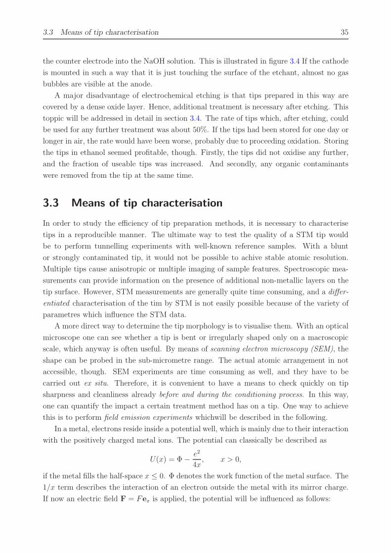
If now an electric field F = Fex is applied, the potential will be influenced as follows:
36 3 The preparation of tunnelling tips
Figure 3.5: The potential experienced by an electron at a metal surface in the presence of
an electric field (solid line). The dashed line is the potential without the effect of the mirror
charge.
U(x) = Φ − e2
4x− Fex, x > 0. (3.2)
The resulting effective potential is sketched in figure 3.5 (the solid line for x > 0). An
electron close to the Fermi level experiences a more or less triangular-shaped potential
barrier which it can overcome by tunnelling. The higher the magnitude of the field, the
narrower is the barrier, resulting in a higher transmission probability T . In 1928, Fowler
and Nordheim published an expression for the field emission current density j as a function
of F and Φ [29, 30, 31, 32]:
j =e3
2πh
(EF/Φ)12
ξ2(EF + Φ)F 2 exp
−8π√
2m
3eh
ξ Φ32
F
(3.3)
The parametre ξ ≤ 1 is a correction which accounts for the interaction of an electron
outside the metal with its mirror charge, i.e. the deviation from the simple triangular
potential well (dashed line in figure 3.5. Note that ξ depends only on the lowering of the
potential barrier Φeff = Φ −√eF due to the applied field[31]. The Fowler-Nordheim
equation (3.3) describes field emission from a infinite plane emitter under high electric fields
in the low temperature limit, but it can also be used to approximate the emission from a
tip-shaped metal at higher temperatures. The idea is now to relate the emission current to
the geometry of the emitter. Approximating the tip geometry by a sphere of radius r at the
end of a cone-shaped shank, the electric field at the tip surface can be written as[33]
F =V
kr, (3.4)
3.3 Means of tip characterisation 37
0 100 200 300 400 500 0
1
2
3
4
5
6
7
8
9 E
mis
sio
n c
urr
ent
/ nA
Voltage / V
tip A tip B
Figure 3.6: Field emission current vs. voltage for two W tips
where V is the applied voltage, and k is a geometrical factor which takes the shank into
consideration. An appropriate value is k ≈ 5[33, 29]. Inserting numerical values for the
constants in equation 3.3 yields for the total emission current
I ∝(
V
r
)2
exp
−6.8 · 109Φ3/2 ξkr
V
(3.5)
for Φ in eV , V in volts, and the tip radius r in metres.
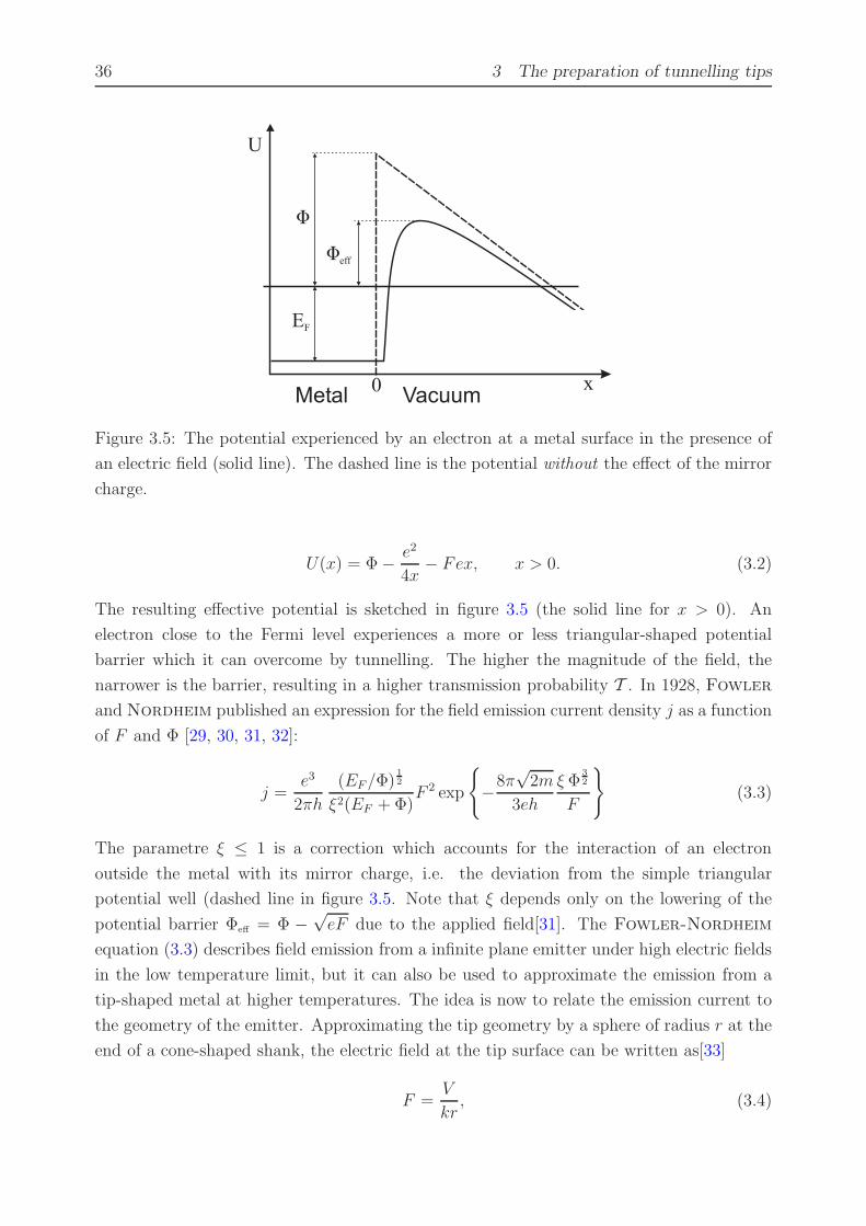
Now figure 3.6 shows the measured field emission current vs. voltage of two tungsten tips.
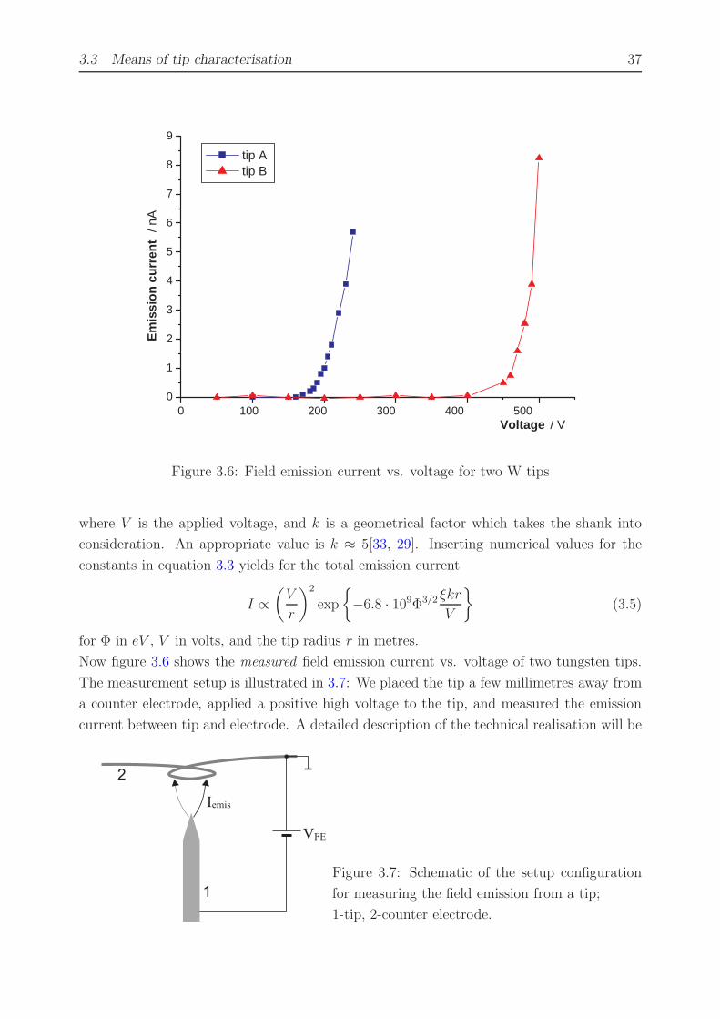
The measurement setup is illustrated in 3.7: We placed the tip a few millimetres away from
a counter electrode, applied a positive high voltage to the tip, and measured the emission
current between tip and electrode. A detailed description of the technical realisation will be
Figure 3.7: Schematic of the setup configuration
for measuring the field emission from a tip;
1-tip, 2-counter electrode.
38 3 The preparation of tunnelling tips
2,0 2,5 4,0 4,5 5,0 5,5 -16
-15
-14
-13
-12
-11
-10
-9
ln(I
/V 2 )
Inverse voltage / (kV) -1
tip A tip B
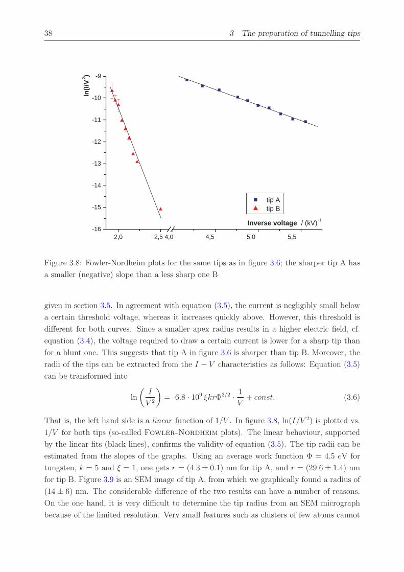
Figure 3.8: Fowler-Nordheim plots for the same tips as in figure 3.6; the sharper tip A has
a smaller (negative) slope than a less sharp one B
given in section 3.5. In agreement with equation (3.5), the current is negligibly small below
a certain threshold voltage, whereas it increases quickly above. However, this threshold is
different for both curves. Since a smaller apex radius results in a higher electric field, cf.
equation (3.4), the voltage required to draw a certain current is lower for a sharp tip than
for a blunt one. This suggests that tip A in figure 3.6 is sharper than tip B. Moreover, the
radii of the tips can be extracted from the I − V characteristics as follows: Equation (3.5)
can be transformed into
ln
(
I
V 2
)
= -6.8 · 109 ξkrΦ3/2 · 1
V+ const. (3.6)
That is, the left hand side is a linear function of 1/V . In figure 3.8, ln(I/V 2) is plotted vs.
1/V for both tips (so-called Fowler-Nordheim plots). The linear behaviour, supported
by the linear fits (black lines), confirms the validity of equation (3.5). The tip radii can be
estimated from the slopes of the graphs. Using an average work function Φ = 4.5 eV for
tungsten, k = 5 and ξ = 1, one gets r = (4.3 ± 0.1) nm for tip A, and r = (29.6 ± 1.4) nm
for tip B. Figure 3.9 is an SEM image of tip A, from which we graphically found a radius of
(14 ± 6) nm. The considerable difference of the two results can have a number of reasons.
On the one hand, it is very difficult to determine the tip radius from an SEM micrograph
because of the limited resolution. Very small features such as clusters of few atoms cannot

3.3 Means of tip characterisation 39
Figure 3.9: SEM image of tip A in figures 3.6 and 3.8. The apex radius is (r = 14 ± 6) nm
be resolved. On the other hand, the values for the constants in equation (3.6) were chosen
rather arbitrarily. In particular, the correction ξ has not yet been considered at all. With
typical voltages of V = 200 V and r = 4 nm for tip A, the field at the tip apex is about
108 V/cm, which, according to Nordheim[31], leads to a correction factor of ξ ≈ 0.4.
Including this into the calculation, the radius extracted from figure 3.8 for tip A becomes
r = (10.9 ± 0.3) nm, i.e. 78% of the value obtained from SEM, which is in reasonable
agreement. It shall be noted that it was possible to get atomic resolution images in STM
with this very same tip. Unfortunately, there is no SEM data available for tip B. However,
estimating ξ in this case would lead to a corrected radius of (37.5 ± 1.8) nm.
Besides extracting the tip radius from a Fowler-Nordheim plot, there is an even
easier way to obtain a crude estimate of the tip sharpness by field emission. For this quick
test it is sufficient to measure just one point at the I−V curve. For a fixed emission current,
equation (3.5) induces a linear dependency of the voltage upon the radius. This can be seen
as follows: Let the function f be defined such that I(V, r) ≡ f(V/r). The inverse function
of f is
f−1 : y 7→ f−1(y) = x, such that f(x) = y
⇒ f−1(I(V, r)) =V
r
That is, for a fixed value Ith of the current, the threshold voltage is proportional to r:
Vth ≡ V (Ith) = f−1(Ith) · r (3.7)
So, in order to estimate the tip sharpness, we placed the tip in the setup described above and
measured the voltage Vth required to draw 1 nA from the tip. The value 1 nA was chosen
such that it lay above the sensitivity limit of our measurement, but still was sufficiently low
40 3 The preparation of tunnelling tips
0 100 200 300 400 5000
5
10
15
20
25
30
35
40Ti
p ra
dius
/ nm
Field emission threshold Vth / V
SEM Field Emission
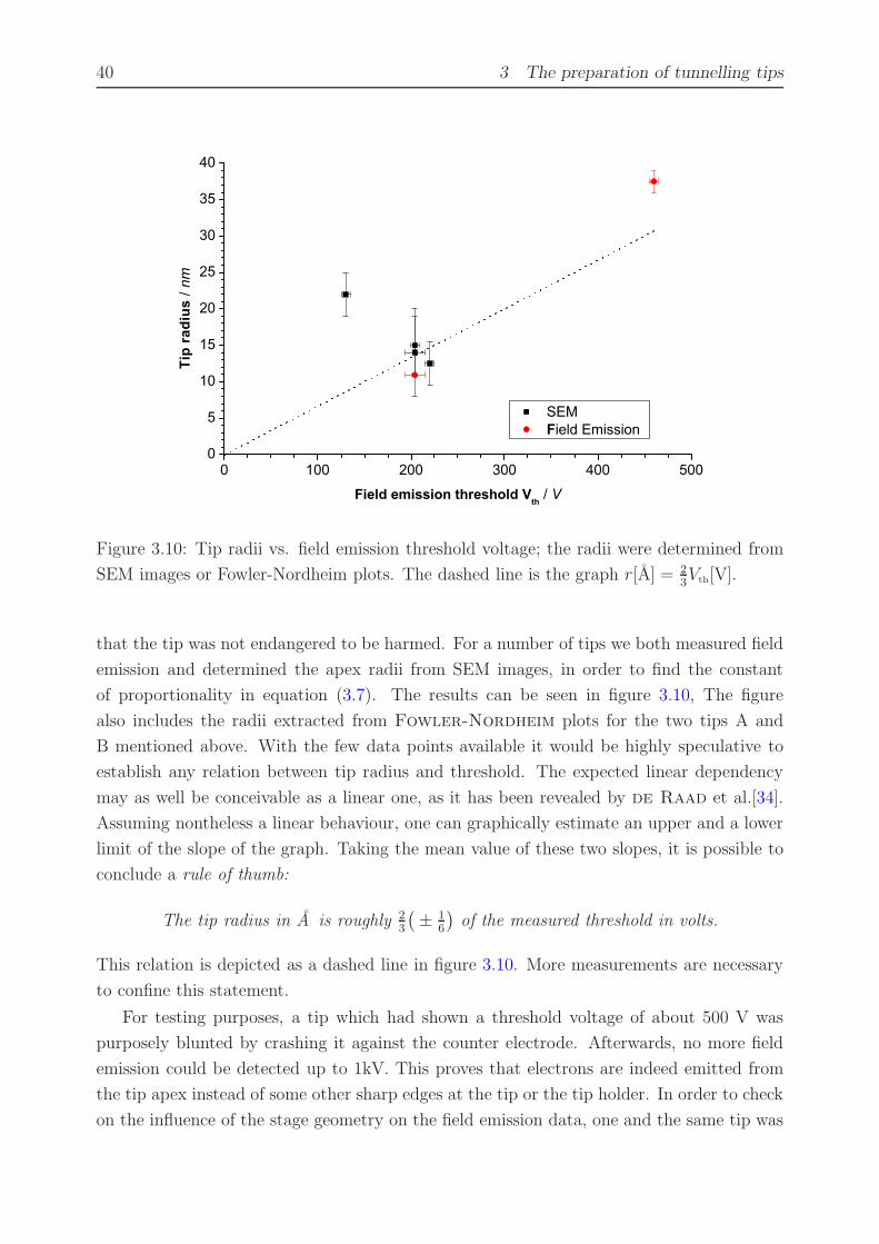
Figure 3.10: Tip radii vs. field emission threshold voltage; the radii were determined from
SEM images or Fowler-Nordheim plots. The dashed line is the graph r[A] = 23Vth[V].
that the tip was not endangered to be harmed. For a number of tips we both measured field
emission and determined the apex radii from SEM images, in order to find the constant
of proportionality in equation (3.7). The results can be seen in figure 3.10, The figure
also includes the radii extracted from Fowler-Nordheim plots for the two tips A and
B mentioned above. With the few data points available it would be highly speculative to
establish any relation between tip radius and threshold. The expected linear dependency
may as well be conceivable as a linear one, as it has been revealed by de Raad et al.[34].
Assuming nontheless a linear behaviour, one can graphically estimate an upper and a lower
limit of the slope of the graph. Taking the mean value of these two slopes, it is possible to
conclude a rule of thumb:
The tip radius in A is roughly 23
(
± 16
)
of the measured threshold in volts.
This relation is depicted as a dashed line in figure 3.10. More measurements are necessary
to confine this statement.
For testing purposes, a tip which had shown a threshold voltage of about 500 V was
purposely blunted by crashing it against the counter electrode. Afterwards, no more field
emission could be detected up to 1kV. This proves that electrons are indeed emitted from
the tip apex instead of some other sharp edges at the tip or the tip holder. In order to check
on the influence of the stage geometry on the field emission data, one and the same tip was
3.3 Means of tip characterisation 41
placed in different positions with respect to the looped counter electrode. Increasing the
relative distance of tip apex and counter electrode by 1 mm caused a change in threshold
voltage from 230 V up to 290 V. Moving the tip parallel to the loop plane by withdrawing
it from the stage for up to 1 mm changed the threshold by as little as 5 V. That is, there
is some influence of the geometry of the experimental setup on the field emission, but it is
not crucial for our purpose: estimating the tip sharpness.
The results presented in this work are based on experiments with more than 70 tungsten
tips. This only includes ”successful” experiments, i.e. only tips which, after etching, were
transferred into the UHV chamber, exposed to some conditioning and characterised using
one or more of the methods mentioned above. Not included are the countless tips which
were lost at some point of the experiment before getting any reliable result. About 50
tips were tested in STM itself. Mostly we used graphite as a standard sample, but also
other samples were tested, such as Au(111) single crystal, NbSe2 and manganite samples.
Selected results are presented in chapter 4. In addition to the STM work, more than 25 tips
were examined by means of SEM. The measurements were carried out ex situ in an XL30
microscope, manufactured by Philips Electron Optics, with a LaB6 cathode. Field emission
tests were only available after the completion of the corresponding facilities described in
section 3.5. Field emission data is available for about 40 tips.
An exact quantisation of the tip shape is not easily possible with the methods in use.
Further information might be gained from transmission electron microscopy (TEM) mea-
surements. However, it is doubtful whether this would be useful because a sharp tip is not
a guarantee for for high resolution STM. Nevertheless, field emission is a simple and quick
tool to check whether a tip may at all be suitable for STM, and one can observe changes
in the tip sharpness due to some treatment procedures. Atomically resolved STM images
could be achieved with tips from a wide range of field emission voltages Vth from 130 to
430 V. Best results were obtained between 150 and 300 V. Following the rule stated above,
these tips had apex radii between 7.5 and 15 nm (or even up to 22.5 nm, assuming the
upper bound). Interestingly, a number of tips which had a very low Vth . 150 V did not
show any decent tunnelling at all. One reason for this might be that very sharp tips are
mechanically unstable. It might also be that the tip had multiple sharp tips or sharp edges
at the apex, which led to a high field emission, but were unfavourable for STM (cf. section
3.1. Above 400 V, we hardly obtained good STM results.
42 3 The preparation of tunnelling tips
3.4 Methods for in-situ tip conditioning
Electrochemical etching yields tips which are microscopically sharp. As mentioned in the
previous section, it is possible to achieve atomic resolution with tips which have apex radii in
the order of 10 nm. It is the aim of tip conditioning to create tips which are as sharp as that,
but equally important is it to get rid of any contaminants which may disturb tunnelling.
During etching and storing the tips under ambient conditions, many kinds of contaminations
can gather at the tungsten surface. In particular, a dense insulating layer is evolving during
the etching procedure[13, 27, 29]. This layer mainly consists of tungsten trioxide WO3, but
also carbon, NaOH conglomerates and WO3−Na microcrystals have been found[35]. The
thickness of these layers can be up to 20nm at the apex[13, 34]. Various techniques have
been suggested to remove these additional tunnelling barriers and to sharpen tips. The
methods include direct and indirect annealing, chemical treatment, sputtering, ultrasonic
cleaning and the application of high electric fields. Not all of the methods seemed to be
promising or applicable to our experimental setups. Therefore, the subsequent presentation
solely includes the methods we investigated at our instruments.
3.4.1 Tip annealing
One widely used way to treat as-etched tips is to anneal them in situ. Water and other sol-
vents are removed at relatively low temperatures already. Above 750 to 800 C, a reduction
of the tungsten trioxide takes place:
2WO3 + W → 3WO2 ↑ (3.8)
The tungsten dioxide is volatile. As the WO3 layer is removed from the tip, a pure tungsten
surface is generated. This reaction takes place far below the melting temperature of tungsten
(3410 C). However, elevated temperatures also enhance the diffusion of surface atoms. This
can lead to blunting of the tip below the melting point[22]. Hence, it is necessary to protect
the tips from being overheated.
We performed tip annealing in two different ways: Direct resistive annealing and heating
by electron bombardment. For direct heating, the tip shank is brought into mechanical
contact with a tungsten filament. The latter is resistively heated, glowing bright orange.
We were not able to observe whether or not the tip itself was glowing, since the filament
was shining far too brightly. However, comparing the brightness of the filament with and
without the tip touching, it could easily be seen that some heat was flowing into the tip
in the former case. The direct annealing method is relatively easy to perform. A piece of
0.2 mm tungsten wire used as a filament inside the vacuum chamber is heated by means
of a standard dc power supply. A disadvantage, however, is that the process is difficult to
control. The whole tip shank is being heated up, and the exact heat flowing to the apex
cannot be predicted. Tips may accidently be molten if heated too strongly. When bringing
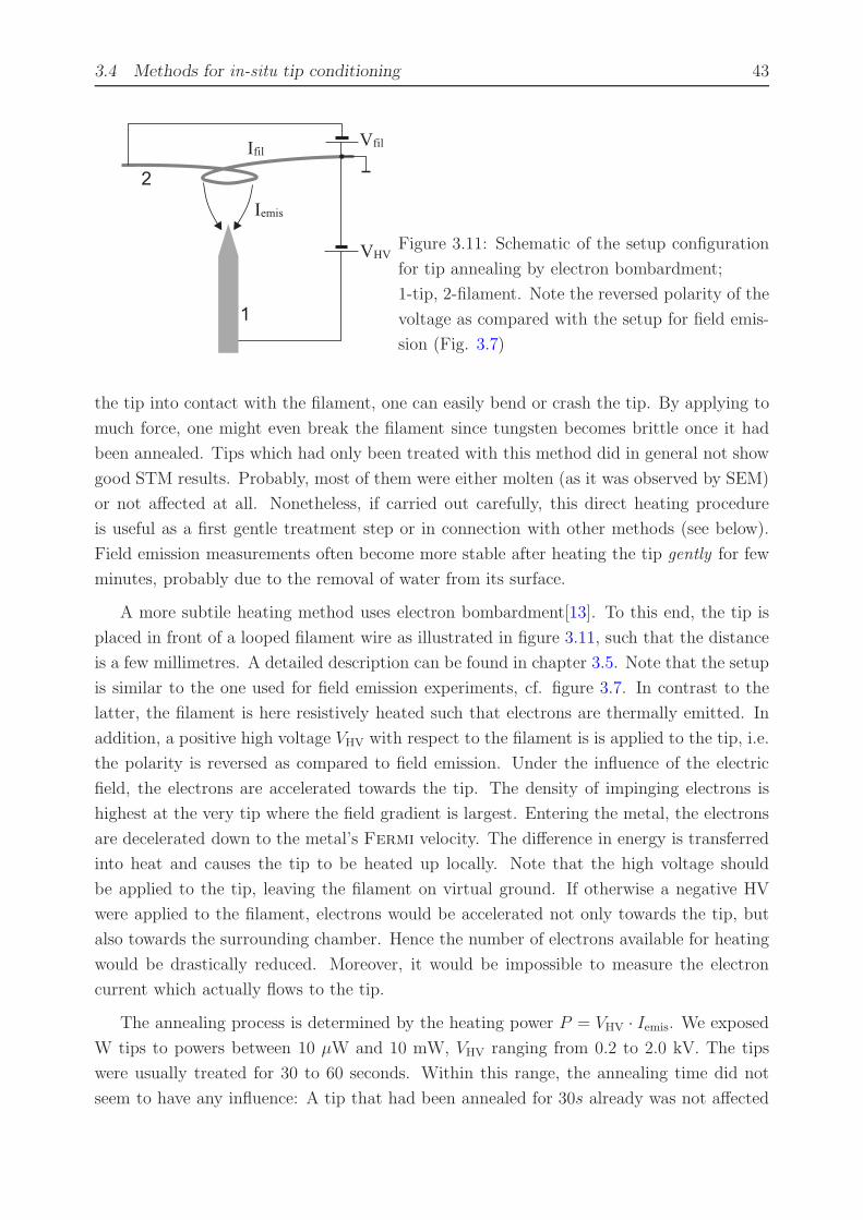
3.4 Methods for in-situ tip conditioning 43
Figure 3.11: Schematic of the setup configuration
for tip annealing by electron bombardment;
1-tip, 2-filament. Note the reversed polarity of the
voltage as compared with the setup for field emis-
sion (Fig. 3.7)
the tip into contact with the filament, one can easily bend or crash the tip. By applying to
much force, one might even break the filament since tungsten becomes brittle once it had
been annealed. Tips which had only been treated with this method did in general not show
good STM results. Probably, most of them were either molten (as it was observed by SEM)
or not affected at all. Nonetheless, if carried out carefully, this direct heating procedure
is useful as a first gentle treatment step or in connection with other methods (see below).
Field emission measurements often become more stable after heating the tip gently for few
minutes, probably due to the removal of water from its surface.
A more subtile heating method uses electron bombardment[13]. To this end, the tip is
placed in front of a looped filament wire as illustrated in figure 3.11, such that the distance
is a few millimetres. A detailed description can be found in chapter 3.5. Note that the setup
is similar to the one used for field emission experiments, cf. figure 3.7. In contrast to the
latter, the filament is here resistively heated such that electrons are thermally emitted. In
addition, a positive high voltage VHV with respect to the filament is is applied to the tip, i.e.
the polarity is reversed as compared to field emission. Under the influence of the electric
field, the electrons are accelerated towards the tip. The density of impinging electrons is
highest at the very tip where the field gradient is largest. Entering the metal, the electrons
are decelerated down to the metal’s Fermi velocity. The difference in energy is transferred
into heat and causes the tip to be heated up locally. Note that the high voltage should
be applied to the tip, leaving the filament on virtual ground. If otherwise a negative HV
were applied to the filament, electrons would be accelerated not only towards the tip, but
also towards the surrounding chamber. Hence the number of electrons available for heating
would be drastically reduced. Moreover, it would be impossible to measure the electron
current which actually flows to the tip.
The annealing process is determined by the heating power P = VHV · Iemis. We exposed
W tips to powers between 10 µW and 10 mW, VHV ranging from 0.2 to 2.0 kV. The tips
were usually treated for 30 to 60 seconds. Within this range, the annealing time did not
seem to have any influence: A tip that had been annealed for 30s already was not affected
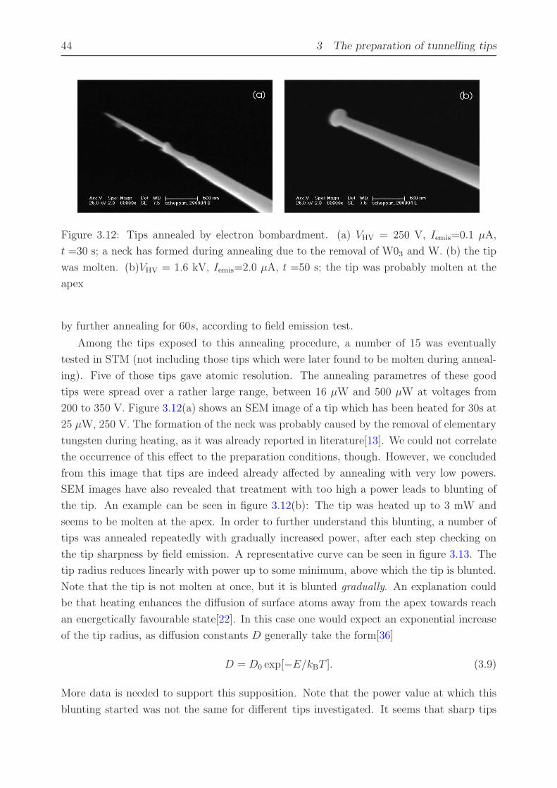
44 3 The preparation of tunnelling tips
Figure 3.12: Tips annealed by electron bombardment. (a) VHV = 250 V, Iemis=0.1 µA,
t =30 s; a neck has formed during annealing due to the removal of W03 and W. (b) the tip
was molten. (b)VHV = 1.6 kV, Iemis=2.0 µA, t =50 s; the tip was probably molten at the
apex
by further annealing for 60s, according to field emission test.
Among the tips exposed to this annealing procedure, a number of 15 was eventually
tested in STM (not including those tips which were later found to be molten during anneal-
ing). Five of those tips gave atomic resolution. The annealing parametres of these good
tips were spread over a rather large range, between 16 µW and 500 µW at voltages from
200 to 350 V. Figure 3.12(a) shows an SEM image of a tip which has been heated for 30s at
25 µW, 250 V. The formation of the neck was probably caused by the removal of elementary
tungsten during heating, as it was already reported in literature[13]. We could not correlate
the occurrence of this effect to the preparation conditions, though. However, we concluded
from this image that tips are indeed already affected by annealing with very low powers.
SEM images have also revealed that treatment with too high a power leads to blunting of
the tip. An example can be seen in figure 3.12(b): The tip was heated up to 3 mW and
seems to be molten at the apex. In order to further understand this blunting, a number of
tips was annealed repeatedly with gradually increased power, after each step checking on
the tip sharpness by field emission. A representative curve can be seen in figure 3.13. The
tip radius reduces linearly with power up to some minimum, above which the tip is blunted.
Note that the tip is not molten at once, but it is blunted gradually. An explanation could
be that heating enhances the diffusion of surface atoms away from the apex towards reach
an energetically favourable state[22]. In this case one would expect an exponential increase
of the tip radius, as diffusion constants D generally take the form[36]
D = D0 exp[−E/kBT ]. (3.9)
More data is needed to support this supposition. Note that the power value at which this
blunting started was not the same for different tips investigated. It seems that sharp tips

3.4 Methods for in-situ tip conditioning 45
0 1 2 3 4 5 6 400
450
500
550
600 F
ield
em
issi
on
th
resh
old
V th
/ V
Annealing power / mW
Figure 3.13: Influence of the annealing power on the tip sharpness: The tip was annealed
with gradually increasing power. After each heating cycle, field emission was measured.
start blunting at lower powers than less sharp ones, but so far, we could not correlate the
situation of the minimum to properties of the tip. Typically, blunting starts between 0.5
and 1.5 mW , in some cases even at lower power. More measurements are necessary to
confine this upper limit. In order to anneal the tips effectively without risking to blunt
them, powers between 20 µW and 100 µW (Iemis = 0.1 to 0.5 µA at 200 V) seem to be most
promising. Within this work, only a few experiments were carried out at very high voltages
(>1 kV). The effect of high electric fields on the annealing process may be worth studying
in more detail (compare also section 3.4.3).
In conclusion, heating by electron bombardment seems to be more suitable for the fragile
STM tips. The annealing conditions are well-controllable, and only the very tip is affected by
this method. According to the reaction (3.8), tungsten oxide as well as elementary tungsten
are removed, leading to a cleaning and sharpening of the tips. However, the sharpening
effect is limited to the removal of a rather thin layer, and an initial sharpness of the tips
is therefore required to achieve good results in STM. The overall rate of tips which gave
good results in STM was rather low. The reason might be that tips annealed within a too
wide range of heating parametres are included. Not all tips could be imaged in SEM after
the STM experiments to reveal whether they were blunt. Restricting the procedure to the
parametre range in which good results were obtained is likely to improve the success rate.
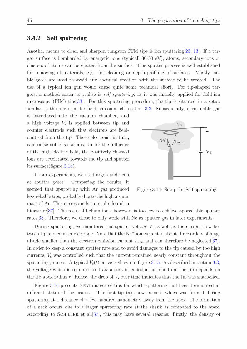
46 3 The preparation of tunnelling tips
3.4.2 Self sputtering
Another means to clean and sharpen tungsten STM tips is ion sputtering[23, 13]. If a tar-
get surface is bombarded by energetic ions (typicall 30-50 eV), atoms, secondary ions or
clusters of atoms can be ejected from the surface. This sputter process is well-established
for removing of materials, e.g. for cleaning or depth-profiling of surfaces. Mostly, no-
ble gases are used to avoid any chemical reaction with the surface to be treated. The
use of a typical ion gun would cause quite some technical effort. For tip-shaped tar-
gets, a method easier to realise is self sputtering, as it was initially applied for field-ion
microscopy (FIM) tips[33]. For this sputtering procedure, the tip is situated in a setup
similar to the one used for field emission, cf. section 3.3. Subsequently, clean noble gas
Figure 3.14: Setup for Self-sputtering
is introduced into the vacuum chamber, and
a high voltage Vs is applied between tip and
counter electrode such that electrons are field-
emitted from the tip. Those electrons, in turn,
can ionise noble gas atoms. Under the influence
of the high electric field, the positively charged
ions are accelerated towards the tip and sputter
its surface(figure 3.14).
In our experiments, we used argon and neon
as sputter gases. Comparing the results, it
seemed that sputtering with Ar gas produced
less reliable tips, probably due to the high atomic
mass of Ar. This corresponds to results found in
literature[37]. The mass of helium ions, however, is too low to achieve appreciable sputter
rates[33]. Therefore, we chose to only work with Ne as sputter gas in later experiments.
During sputtering, we monitored the sputter voltage Vs as well as the current flow be-
tween tip and counter electrode. Note that the Ne+ ion current is about three orders of mag-
nitude smaller than the electron emission current Iemis and can therefore be neglected[37].
In order to keep a constant sputter rate and to avoid damages to the tip caused by too high
currents, Vs was controlled such that the current remained nearly constant throughout the
sputtering process. A typical Vs(t) curve is shown in figure 3.15. As described in section 3.3,
the voltage which is required to draw a certain emission current from the tip depends on
the tip apex radius r. Hence, the drop of Vs over time indicates that the tip was sharpened.
Figure 3.16 presents SEM images of tips for which sputtering had been terminated at
different states of the process. The first tip (a) shows a neck which was formed during
sputtering at a distance of a few hundred nanometres away from the apex. The formation
of a neck occurs due to a larger sputtering rate at the shank as compared to the apex.
According to Schiller et al.[37], this may have several reasons: Firstly, the density of
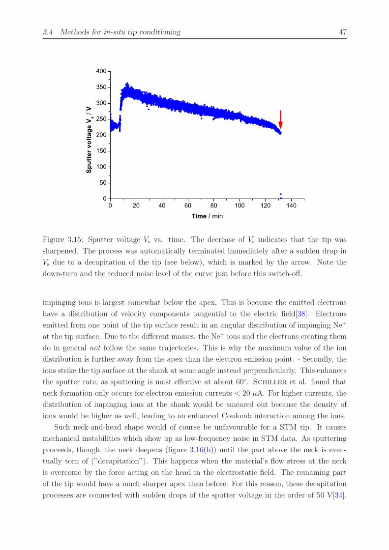
3.4 Methods for in-situ tip conditioning 47
0 20 40 60 80 100 120 1400
50
100
150
200
250
300
350
400
Sput
ter
volta
ge V
s / V
Time / min
Figure 3.15: Sputter voltage Vs vs. time. The decrease of Vs indicates that the tip was
sharpened. The process was automatically terminated immediately after a sudden drop in
Vs due to a decapitation of the tip (see below), which is marked by the arrow. Note the
down-turn and the reduced noise level of the curve just before this switch-off.
impinging ions is largest somewhat below the apex. This is because the emitted electrons
have a distribution of velocity components tangential to the electric field[38]. Electrons
emitted from one point of the tip surface result in an angular distribution of impinging Ne+
at the tip surface. Due to the different masses, the Ne+ ions and the electrons creating them
do in general not follow the same trajectories. This is why the maximum value of the ion
distribution is further away from the apex than the electron emission point. - Secondly, the
ions strike the tip surface at the shank at some angle instead perpendicularly. This enhances
the sputter rate, as sputtering is most effective at about 60. Schiller et al. found that
neck-formation only occurs for electron emission currents < 20 µA. For higher currents, the
distribution of impinging ions at the shank would be smeared out because the density of
ions would be higher as well, leading to an enhanced Coulomb interaction among the ions.
Such neck-and-head shape would of course be unfavourable for a STM tip. It causes
mechanical instabilities which show up as low-frequency noise in STM data. As sputtering
proceeds, though, the neck deepens (figure 3.16(b)) until the part above the neck is even-
tually torn of (”decapitation”). This happens when the material’s flow stress at the neck
is overcome by the force acting on the head in the electrostatic field. The remaining part
of the tip would have a much sharper apex than before. For this reason, these decapitation
processes are connected with sudden drops of the sputter voltage in the order of 50 V[34].
48 3 The preparation of tunnelling tips
Detecting these voltage jumps, it is possible to automatically terminate the sputter process
immediately after a decapitation, resulting in very sharp and clean tips with apex radii of
few nanometres[37], cf figure 3.16(c). Notably, such decapitation of the tip is usually con-
nected with a typical shape of the Vs vs. time curve. Just before the decapitation, one can
often observe an enhanced sharpening rate (indicated by a down-turn of the curve), along
with a reduction of the noise, see figure 3.15. In few cases, the curve also turned up instead
of down shortly before a sudden voltage drop.
Among the tips treated by self-sputtering, a number of 31 were eventually tested in STM.
For ten of them, argon was used as sputter gas, while all the others were sputtered with neon.
Six of the ten tips treated with argon gave atomic resolution on graphite. However, only
for one of them the quality was really satisfactory, that is low noise, sharp features and no
double imaging. From the 21 tips treated with neon gas, twelve showed atomically resolved
images on graphite or gold, six of them in really high quality. Best results were obtained
with tips that showed a field emission threshold Vth between 180 and 250 V, indicating apex
radii of about 10 to 15 nm (cf. figure 3.10 in section 3.3), but occasionally atomic resolution
was obtained up to Vth = 400 V. On the other hand, we noted that tips which appeared
very sharp (Vth . 150 V) frequently did not yield any reasonable resolution at all, as it was
mentioned in section 3.3 already.Furthermore, good results with sputtered tips were almost
exclusively achieved after the occurrence of a tip decapitation described above. Figure 3.17
shows two STM topography images of HOPG. The images were recorded with one and
the same W tip before and after a sputter treatment which ended with a decapitation,
evidencing a distinct improvement in resolution. Contrariwise, tips that had been sputtered
for a longer time without such decapitation did in general not show reasonable imaging.
We frequently noticed considerable oscillations in the order of 25 Hz which were superposed
to the tunnelling signal. Those disturbances were evidently caused by the tip. Probably,
a pronounced neck caused by sputtering as in figure 3.16(b) rendered the tip mechanically
unstable. Similar observations can be found in literature[13]. Attempts to sputter tips just
for few seconds in order to remove contaminants without the formation of any neck did not
succeed either.
Clearly, a higher electron emission from the tip leads to a larger sputter rate. In order to
achieve appreciable sputter rates and at the same time ensure that the formation of a neck
is possible, we chose emission currents between 5 to 20 µA. The power supply in use (cf.
section 3.5.3) is limited to one kilovolt. As a rule of thumb, the voltage required for a field
emission of 10 µA is about 1.5 to 2 times higher than for 1 nA. Hence, only tips with an
initial field emission threshold Vth . 600 V were eligible for sputter treatment in our setup.
During sputtering, the penetrating ions cause damages at the tip surface, frequently
resulting in the formation of multiple tips[13]. Subsequent annealing can cure such damages
and bring the tip into a more stable state[23]. We found that for tips which had been
annealed after self-sputtering, the tunnelling current was generally less noisy, the resolution
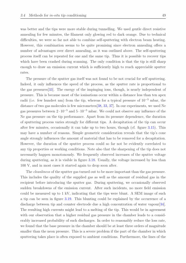
3.4 Methods for in-situ tip conditioning 49
was better and the tips were more stable during tunnelling. We used gentle direct resistive
annealing for few minutes, the filament only glowing red to dark orange. Due to technical
difficulties, we were so far not able to combine self-sputtering with electron beam heating.
However, this combination seems to be quite promising since electron annealing offers a
number of advantages over direct annealing, as it was outlined above. The self-sputtering
process itself can be repeated for one and the same tip. Thus it is possible to recover tips
which have been crashed during scanning. The only condition is that the tip is still sharp
enough to draw an emission current which is sufficiently high to reach appreciable sputter
rates.
The pressure of the sputter gas itself was not found to be not crucial for self sputtering.
Indeed, it only influences the speed of the process, as the sputter rate is proportional to
the gas pressures[33]. The energy of the impinging ions, though, is nearly independent of
pressure. This is because most of the ionisations occur within a distance less than ten apex
radii (i.e. few hundret nm) from the tip, whereas for a typical pressure of 10−3 mbar, the
distance of two gas molecules is few micrometres[38, 33, 37]. In our experiments, we used Ne
gas pressures between 2 · 10−5 and 5 · 10−5 mbar. We could not observe any influence of the
Ne gas pressure on the tip performance. Apart from its pressure dependence, the duration
of sputtering process varies strongly for different tips. A decapitation of the tip can occur
after few minutes, occasionally it can take up to two hours, though (cf. figure 3.15). This
may have a number of reasons. Simple geometric consideration reveals that the tip’s cone
angle strongly influences the amount of material that has to be removed for a decapitation.
However, the duration of the sputter process could so far not be evidently correlated to
any tip properties or working conditions. Note also that the sharpening of the tip does not
necessarily happen monotonously. We frequently observed increases of the sputter voltage
during sputtering, as it is visible in figure 3.18. Usually, the voltage increased by less than
100 V, and in most cases it started again to drop soon after.
The cleanliness of the sputter gas turned out to be more important than the gas pressure.
This includes the quality of the supplied gas as well as the amount of residual gas in the
recipient before introducing the sputter gas. During sputtering, we occasionally observed
sudden breakdowns of the emission current. After such incidents, no more field emission
could be measured up to 1 kV, indicating that the tips were blunt. A SEM image of such
a tip can be seen in figure 3.19. This blunting could be explained by the occurrence of a
discharge between tip and counter electrode due a high concentration of water vapour[34].
The resulting high currents might lead to a melting of the tip. This would be in agreement
with our observation that a higher residual gas pressure in the chamber leads to a consid-
erably increased probability of such discharges. In order to reasonably reduce the loss rate,
we found that the base pressure in the chamber should be at least three orders of magnitude
smaller than the neon pressure. This is a severe problem if the part of the chamber in which
sputtering takes place is often exposed to ambient conditions. Furthermore, the lines of the

50 3 The preparation of tunnelling tips
gas supply ought to be flushed before use.
In summary, the method of self sputtering offers an effective means for tip conditioning.
An increasing neck-formation close to the apex leads to a decapitation of the tip. If the
process is determinated immediately after such incident, the remaining tips are sharp and
free of contaminants. However, it is profitable to subsequently anneal the tips in order to
achieve high quality STM data with a reasonable success rate.
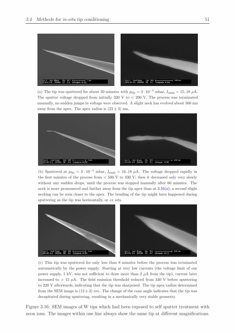
3.4 Methods for in-situ tip conditioning 51
(a) The tip was sputtered for about 30 minutes with pNe = 3 · 10−5 mbar, Iemis = 15..18 µA.
The sputter voltage dropped from initially 320 V to < 200 V. The process was terminated
manually, no sudden jumps in voltage were observed. A slight neck has evolved about 500 nm
away from the apex. The apex radius is (22 ± 3) nm.
(b) Sputtered at pNe = 3 · 10−5 mbar, Iemis = 16..18 µA. The voltage dropped rapidly in
the first minutes of the process from < 500 V to 330 V; then it decreased only very slowly
without any sudden drops, until the process was stopped manually after 60 minutes. The
neck is more pronounced and further away from the tip apex than at 3.16(a); a second slight
necking can be seen closer to the apex. The bending of the tip might have happened during
sputtering as the tip was horizontally, or ex situ.
(c) This tip was sputtered for only less than 8 minutes before the process was terminated
automatically by the power supply. Starting at very low currents (the voltage limit of our
power supply, 1 kV, was not sufficient to draw more than 2 µA from the tip), current later
increased to > 15 µA. The field emission threshold reduced from 340 V before sputtering
to 220 V afterwards, indicating that the tip was sharpened. The tip apex radius determined
from the SEM image is (12± 3) nm. The change of the cone angle indicates that the tip was
decapitated during sputtering, resulting in a mechanically very stable geometry.
Figure 3.16: SEM images of W tips which had been exposed to self sputter treatment with
neon ions. The images within one line always show the same tip at different magnifications.
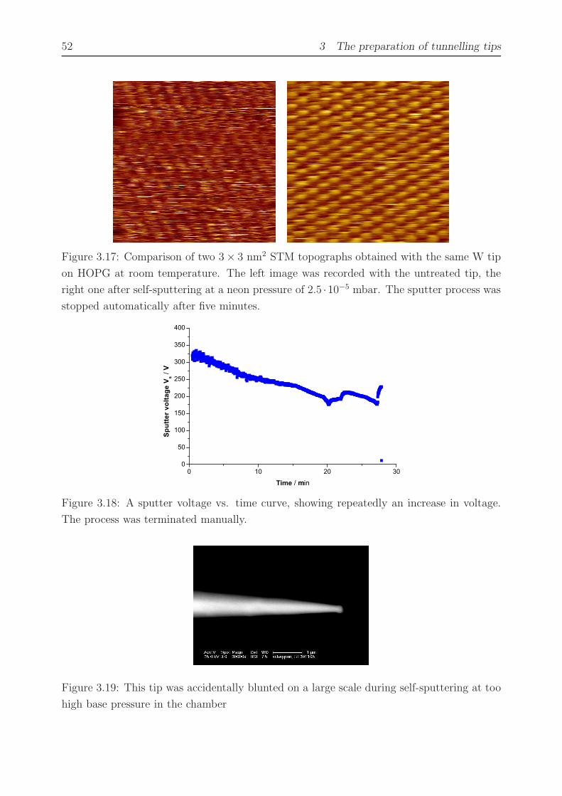
52 3 The preparation of tunnelling tips
Figure 3.17: Comparison of two 3 × 3 nm2 STM topographs obtained with the same W tip
on HOPG at room temperature. The left image was recorded with the untreated tip, the
right one after self-sputtering at a neon pressure of 2.5 ·10−5 mbar. The sputter process was
stopped automatically after five minutes.
0 10 20 300
50
100
150
200
250
300
350
400
Sput
ter
volta
ge V
s / V
Time / min
Figure 3.18: A sputter voltage vs. time curve, showing repeatedly an increase in voltage.
The process was terminated manually.
Figure 3.19: This tip was accidentally blunted on a large scale during self-sputtering at too
high base pressure in the chamber
3.4 Methods for in-situ tip conditioning 53
3.4.3 The influence of an electric field on the tip
Even though the overall shape of an etched tungsten tip is quite stable, it is subject to
permanent changes on an atomic scale. Atoms can diffuse along the surface, be evaporated
from the surface, or atoms from the gas phase can be adsorbed on the tip surface. On
the one hand, this may lead to undesirable effects during experiments. Changes in the
atomic configuration or contaminations migrating towards the very tip apex may disturb
data acquisition. Working at low temperatures may reduce such effects since the diffusion
depends exponentially upon activation energy (cf. equation (3.9 in section 3.4.1).
On the other hand, the latter effects can be beneficial for tip preparation if applied in a
controlled manner. As shown by Fink, it is possible to create mono-atomic tungsten tips
using field evaporation[21]. Carefully adjusting the tip potential, one atomic layer after the
other could be removed from the surface of a single-crystalline tungsten tip. The process
was carried out and monitored in a FIM setup with electric fields in the order of 4 V/A.
This procedure is technically very demanding, though.
At a sharp tip, thermal diffusion creates a flux of atoms which is directed away from
the apex. With a strong electric field, the direction can be reversed, though[14]. Under
the influence of an external field F, atoms at the metal surface are polarised[39, 40]. The
resulting dipole moment p is proportional to the field, p = αF, the constant α being the
polarisability. The potential energy of such a polarisation is
W =1
2p · F =
1
2αF 2 (F = |F|) (3.10)
In an inhomogeneous field, as it is present at the apex of a sharp tip, such dipoles experience
a force
K = −∇W = αF (∇F ) (3.11)
Note that field enters equation (3.11) quadratically. This force is always directed towards
the highest field. Accordingly, the field induces a diffusion flux towards the tip apex, in-
dependently of the polarity. This diffusion can be used to alter the atomic configuration:
During tunnelling in an STM, the field strength between tip and sample is large also for
moderate gap voltages due to the small tunnelling gap of less than 1 nm. A widely used way
of tip treatment inside the STM is to strongly increase the voltage for a short time while the
tip remains in proximity to the sample. To our experience, this procedure is helpful for tips
which are sharp but do not show satisfactory resolution. Applying 5 to 10 V for few seconds
was sometimes sufficient to change a tip in a profitable way. It seems to be promising to
apply this procedure in connection with other methods, as to ”put the finishing touch”,
or to recover tips which have changed during scanning. A higher voltage in the order of
50 to 80 V may be more effective to improve our tips[41]. However, the pre-amplifiers in
use at our STM’s are limited to Vgap = ±10 V. We are, therefore, planning on altering our
electronic setup, in order to be able to apply higher voltages.

54 3 The preparation of tunnelling tips
3.5 Facilities for in-situ tip conditioning
Part of the experimental task of this work was the design and construction of facilities for
in-situ tip conditioning for both our STM systems. The aim was the reliable fabrication of
tips yielding high resolution and low noise STM data by choosing one, or a combination of
methods described in the previous sections. The entirely different designs of the two STM
and, specifically, of the respective tip holders demanded for different solutions for the tip
conditioning stages as well. Either design will be described in this section.
In both systems, the stages for tip treatment were mounted in the load lock chambers.
The advantage is that one can carry out tip conditioning without opening the main UHV
chamber. The loadlock can be evacuated separately with turbo pumps. Within a few
minutes, the pressure normally reaches the 10−6 mbar range, which is sufficiently low for a
first careful field emission test. If the tip is found to be sharp enough, the loadlock can be
pumped further until the working pressure for tip conditioning (10−8 mbar range) is reached.
Otherwise the tip can be replaced by a new one without loosing overly much time. The
load lock chamber of the VT-STM can be seen in figure 3.21. The design of the chambers is
similar for both STM’s. In either case, the tip conditioning stage was mounted on a stainless
steel angle which was attached to a CF40 port, cf. figure 3.20. The stage can be retracted
by a linear drive such that tips or samples can be transferred into the main chamber using
a manipulator.
On top of the construction of the stages for tip conditioning, some additional technical
requirements were to be provided. A power supply was designed for field emission experi-
ments and self-sputtering of tips. The power supply will be described in section 3.5.3. The
gas supplies of the UHV recipients had to be added or addapted, cf. figure A.1 on 80, and
modifications had to be made to the loadlock vacuum chambers.
3.5.1 Tip conditioning at the Cryogenic STM
A shown in figure 3.20, there are two places to put tip holders. The dovetail openings were
made by electrical discharge machining (EDM) from a piece of stainless steel. At the left
place, the tip is situated beneath a looped 0.2 mm diameter tungsten wire. This loop serves
as counter electrode for self sputtering and field emission tests, and as both filament and
counter electrode for tip annealing by electron bombardment. The loop has a diameter of
2-3 mm, and it is a few millimetres away from the tip end, depending on the tip length.
One end of the looped wire is connected to a current feedthrough whereas the other end is
at ground. The high voltage is in any case supplied to the tip, leaving the counter electrode
at ground potential. Otherwise, there might a undesired flow of electrons between counter
electrode and the surrounding UHV chamber or other metal parts in the environment. The
second position for tip holders is designed for direct annealing of the tip. A piece of tungsten
wire is positioned in such a way that it touches the tip shank 1-2 mm below the tip’s apex.
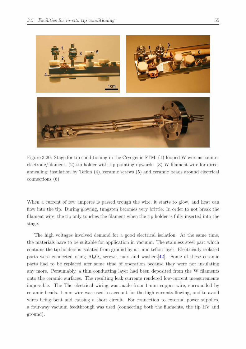
3.5 Facilities for in-situ tip conditioning 55
Figure 3.20: Stage for tip conditioning in the Cryogenic STM. (1)-looped W wire as counter
electrode/filament, (2)-tip holder with tip pointing upwards, (3)-W filament wire for direct
annealing; insulation by Teflon (4), ceramic screws (5) and ceramic beads around electrical
connections (6)
When a current of few amperes is passed trough the wire, it starts to glow, and heat can
flow into the tip. During glowing, tungsten becomes very brittle. In order to not break the
filament wire, the tip only touches the filament when the tip holder is fully inserted into the
stage.
The high voltages involved demand for a good electrical isolation. At the same time,
the materials have to be suitable for application in vacuum. The stainless steel part which
contains the tip holders is isolated from ground by a 1 mm teflon layer. Electrically isolated
parts were connected using Al2O3 screws, nuts and washers[42]. Some of these ceramic
parts had to be replaced afer some time of operation because they were not insulating
any more. Persumably, a thin conducting layer had been deposited from the W filaments
onto the ceramic surfaces. The resulting leak currents rendered low-current measurements
impossible. The The electrical wiring was made from 1 mm copper wire, surrounded by
ceramic beads. 1 mm wire was used to account for the high currents flowing, and to avoid
wires being bent and causing a short circuit. For connection to external power supplies,
a four-way vacuum feedthrough was used (connecting both the filaments, the tip HV and
ground).
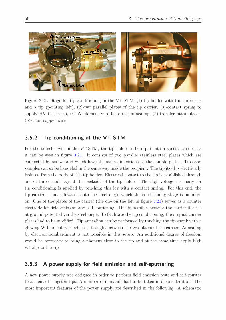
56 3 The preparation of tunnelling tips
Figure 3.21: Stage for tip conditioning in the VT-STM. (1)-tip holder with the three legs
and a tip (pointing left), (2)-two parallel plates of the tip carrier, (3)-contact spring to
supply HV to the tip, (4)-W filament wire for direct annealing, (5)-transfer manipulator,
(6)-1mm copper wire
3.5.2 Tip conditioning at the VT-STM
For the transfer within the VT-STM, the tip holder is here put into a special carrier, as
it can be seen in figure 3.21. It consists of two parallel stainless steel plates which are
connected by screws and which have the same dimensions as the sample plates. Tips and
samples can so be handeled in the same way inside the recipient. The tip itself is electrically
isolated from the body of this tip holder. Electrical contact to the tip is established through
one of three small legs at the backside of the tip holder. The high voltage necessary for
tip conditioning is applied by touching this leg with a contact spring. For this end, the
tip carrier is put sidewards onto the steel angle which the conditioning stage is mounted
on. One of the plates of the carrier (the one on the left in figure 3.21) serves as a counter
electrode for field emission and self-sputtering. This is possible because the carrier itself is
at ground potential via the steel angle. To facilitate the tip conditioning, the original carrier
plates had to be modified. Tip annealing can be performed by touching the tip shank with a
glowing W filament wire which is brought between the two plates of the carrier. Annealing
by electron bombardment is not possible in this setup. An additional degree of freedom
would be necessary to bring a filament close to the tip and at the same time apply high
voltage to the tip.
3.5.3 A power supply for field emission and self-sputtering
A new power supply was designed in order to perform field emission tests and self-sputter
treatment of tungsten tips. A number of demands had to be taken into consideration. The
most important features of the power supply are described in the following. A schematic
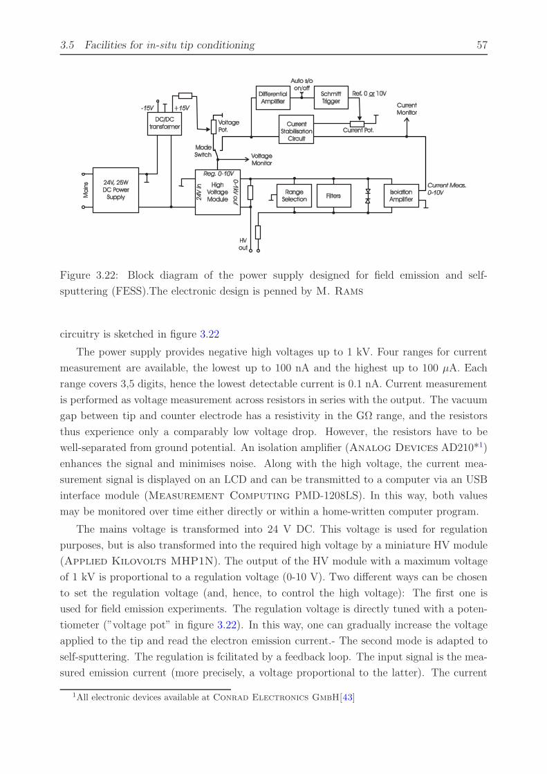
3.5 Facilities for in-situ tip conditioning 57
Differential
Amplifier
Auto s/o
on/off
High
Voltage
Module
24V, 25W
DC Power
Supply
DC/DC
transformer
Isolation
AmplifierFilters
Current
Monitor
Voltage
Monitor
Voltage
Pot.
Mode
Switch
Current Pot.
-15V +15V
Current Meas.
0-10V
Reg. 0-10V
24
V in
0-1
kV o
uf
Ref. 0 10Vor
HV
out
Range
Selection
Current
Stabilisation
Circuit
Schmitt
Trigger
Ma
ins
Figure 3.22: Block diagram of the power supply designed for field emission and self-
sputtering (FESS).The electronic design is penned by M. Rams
circuitry is sketched in figure 3.22
The power supply provides negative high voltages up to 1 kV. Four ranges for current
measurement are available, the lowest up to 100 nA and the highest up to 100 µA. Each
range covers 3,5 digits, hence the lowest detectable current is 0.1 nA. Current measurement
is performed as voltage measurement across resistors in series with the output. The vacuum
gap between tip and counter electrode has a resistivity in the GΩ range, and the resistors
thus experience only a comparably low voltage drop. However, the resistors have to be
well-separated from ground potential. An isolation amplifier (Analog Devices AD210*1)
enhances the signal and minimises noise. Along with the high voltage, the current mea-
surement signal is displayed on an LCD and can be transmitted to a computer via an USB
interface module (Measurement Computing PMD-1208LS). In this way, both values
may be monitored over time either directly or within a home-written computer program.
The mains voltage is transformed into 24 V DC. This voltage is used for regulation
purposes, but is also transformed into the required high voltage by a miniature HV module
(Applied Kilovolts MHP1N). The output of the HV module with a maximum voltage
of 1 kV is proportional to a regulation voltage (0-10 V). Two different ways can be chosen
to set the regulation voltage (and, hence, to control the high voltage): The first one is
used for field emission experiments. The regulation voltage is directly tuned with a poten-
tiometer (”voltage pot” in figure 3.22). In this way, one can gradually increase the voltage
applied to the tip and read the electron emission current.- The second mode is adapted to
self-sputtering. The regulation is fcilitated by a feedback loop. The input signal is the mea-
sured emission current (more precisely, a voltage proportional to the latter). The current
1All electronic devices available at Conrad Electronics GmbH[43]

58 3 The preparation of tunnelling tips
stabilisation circuit, containing a differential amplifier, regulates the voltage in such a way
that the emission current drawn from the tip during sputtering remains (nearly) constant.
A second control loop is responsible for the automatic switch-off of the sputter process in
case of a tip decapitation (cf. section 3.4.2. The output of the current stabilisation circuit
is fed via a differential amplifier into a so-called Schmitt trigger. This module sets the
regulation voltage to zero in case of a drastic change of its input signal. As a matter of
fact, sudden sudden drop of the sputter voltage, as in figure 3.15, can be detected, and the
sputter process can be terminated accordingly. This automatic switch-off can be disabled.
By means of a potentiometer (”current pot”), the regulation voltage can be tuned. In this
way one can determine the current setpoint for which the high voltage is stabilised.
The vacuum gap between tip and counter electrode has a huge electrical resistance. For
a typical field emission current of 1 nA at a tip voltage of 500 V, the equivalent ohmic
resistance would be 500 GΩ. Hence, one cannot use conventional cable because the leak
current through the isolation would quickly exceed the low field emission currents. We
therefore used Teflon isolated cable. The cable should also be as short as possible in order
to minimise the leak current. In this way, also charging effects due to the capacitance of
the cable would be reduced. Another problem connected with the high resistance are leak
currents on the circuit board inside the power supply. We noted that on days with high
air humidity, the level of parasitic leak current was considerably enhanced. Protecting the
sensitive regions with nitro varnish helped temporarily. Over time, however, the varnish
absorbed moisture, again causing leak currents. Finally, the problem could be solved by
coating the entire board with hot glue.
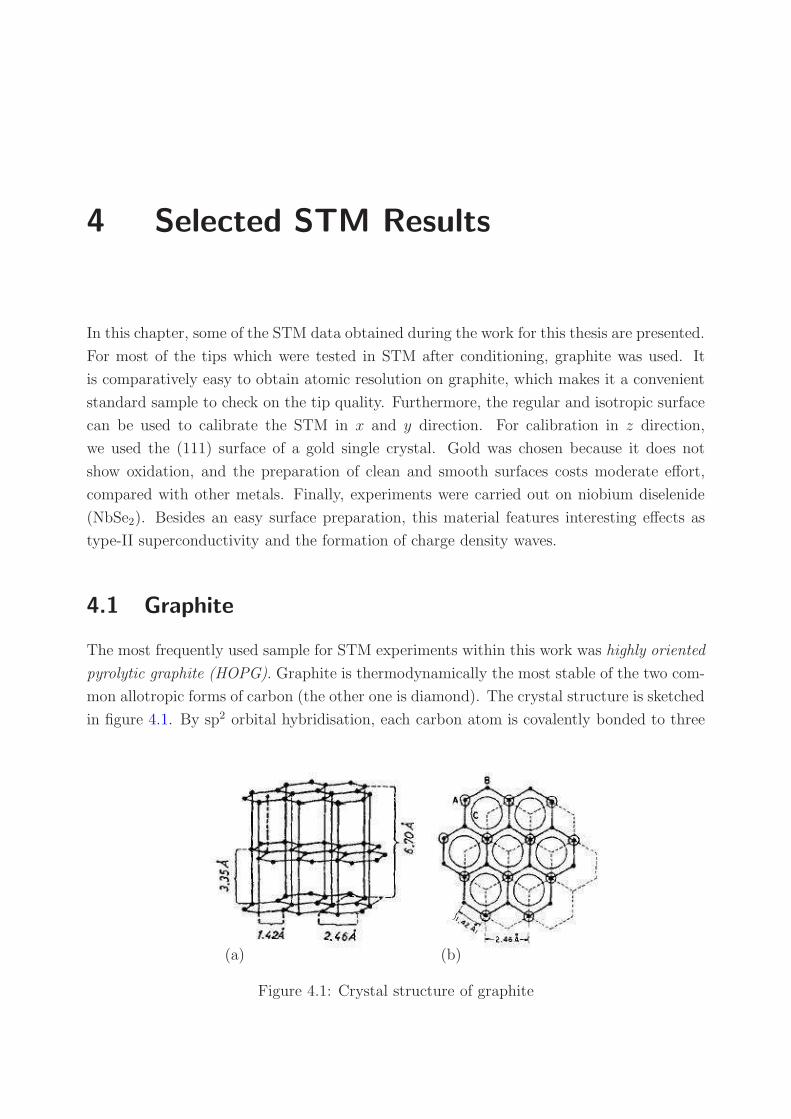
4 Selected STM Results
In this chapter, some of the STM data obtained during the work for this thesis are presented.
For most of the tips which were tested in STM after conditioning, graphite was used. It
is comparatively easy to obtain atomic resolution on graphite, which makes it a convenient
standard sample to check on the tip quality. Furthermore, the regular and isotropic surface
can be used to calibrate the STM in x and y direction. For calibration in z direction,
we used the (111) surface of a gold single crystal. Gold was chosen because it does not
show oxidation, and the preparation of clean and smooth surfaces costs moderate effort,
compared with other metals. Finally, experiments were carried out on niobium diselenide
(NbSe2). Besides an easy surface preparation, this material features interesting effects as
type-II superconductivity and the formation of charge density waves.
4.1 Graphite
The most frequently used sample for STM experiments within this work was highly oriented
pyrolytic graphite (HOPG). Graphite is thermodynamically the most stable of the two com-
mon allotropic forms of carbon (the other one is diamond). The crystal structure is sketched
in figure 4.1. By sp2 orbital hybridisation, each carbon atom is covalently bonded to three
(a) (b)
Figure 4.1: Crystal structure of graphite
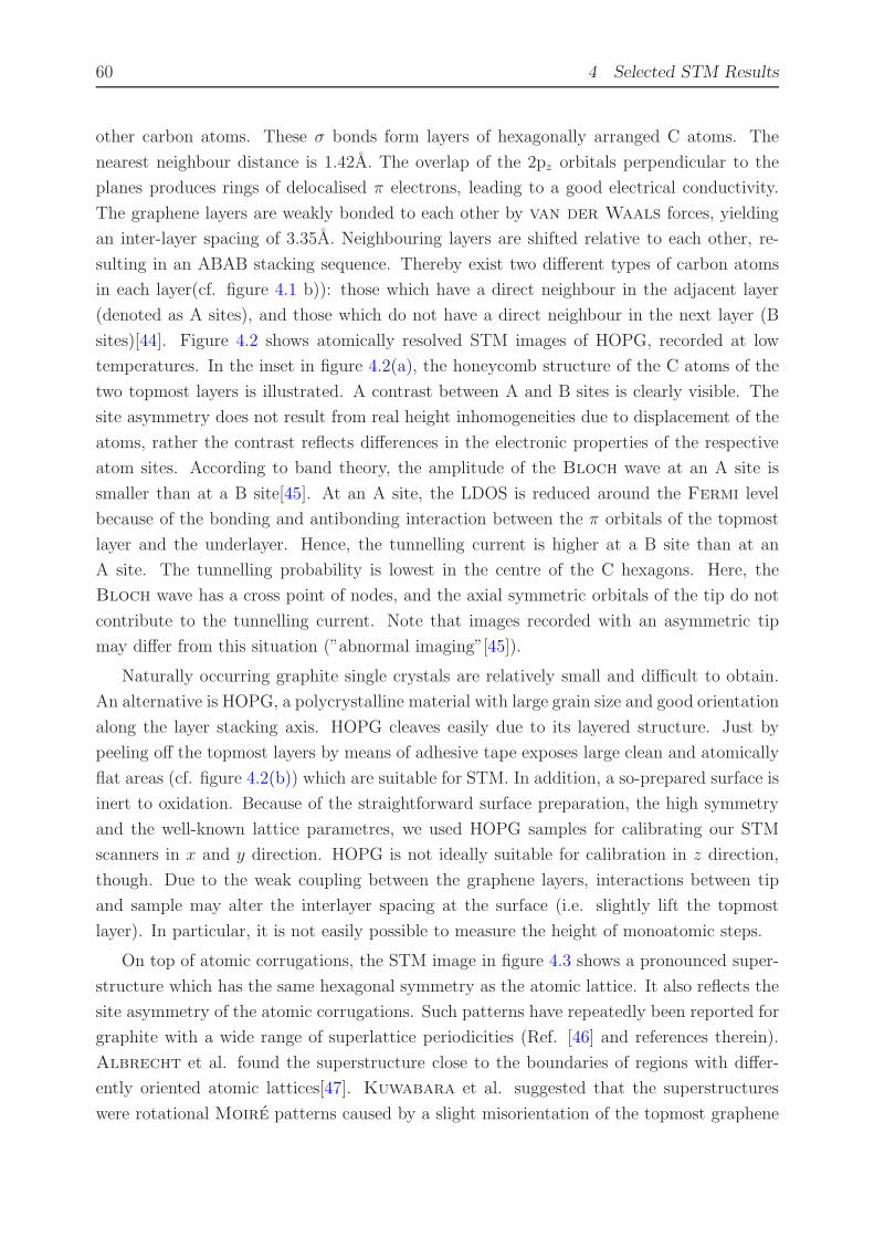
60 4 Selected STM Results
other carbon atoms. These σ bonds form layers of hexagonally arranged C atoms. The
nearest neighbour distance is 1.42A. The overlap of the 2pz orbitals perpendicular to the
planes produces rings of delocalised π electrons, leading to a good electrical conductivity.
The graphene layers are weakly bonded to each other by van der Waals forces, yielding
an inter-layer spacing of 3.35A. Neighbouring layers are shifted relative to each other, re-
sulting in an ABAB stacking sequence. Thereby exist two different types of carbon atoms
in each layer(cf. figure 4.1 b)): those which have a direct neighbour in the adjacent layer
(denoted as A sites), and those which do not have a direct neighbour in the next layer (B
sites)[44]. Figure 4.2 shows atomically resolved STM images of HOPG, recorded at low
temperatures. In the inset in figure 4.2(a), the honeycomb structure of the C atoms of the
two topmost layers is illustrated. A contrast between A and B sites is clearly visible. The
site asymmetry does not result from real height inhomogeneities due to displacement of the
atoms, rather the contrast reflects differences in the electronic properties of the respective
atom sites. According to band theory, the amplitude of the Bloch wave at an A site is
smaller than at a B site[45]. At an A site, the LDOS is reduced around the Fermi level
because of the bonding and antibonding interaction between the π orbitals of the topmost
layer and the underlayer. Hence, the tunnelling current is higher at a B site than at an
A site. The tunnelling probability is lowest in the centre of the C hexagons. Here, the
Bloch wave has a cross point of nodes, and the axial symmetric orbitals of the tip do not
contribute to the tunnelling current. Note that images recorded with an asymmetric tip
may differ from this situation (”abnormal imaging”[45]).
Naturally occurring graphite single crystals are relatively small and difficult to obtain.
An alternative is HOPG, a polycrystalline material with large grain size and good orientation
along the layer stacking axis. HOPG cleaves easily due to its layered structure. Just by
peeling off the topmost layers by means of adhesive tape exposes large clean and atomically
flat areas (cf. figure 4.2(b)) which are suitable for STM. In addition, a so-prepared surface is
inert to oxidation. Because of the straightforward surface preparation, the high symmetry
and the well-known lattice parametres, we used HOPG samples for calibrating our STM
scanners in x and y direction. HOPG is not ideally suitable for calibration in z direction,
though. Due to the weak coupling between the graphene layers, interactions between tip
and sample may alter the interlayer spacing at the surface (i.e. slightly lift the topmost
layer). In particular, it is not easily possible to measure the height of monoatomic steps.
On top of atomic corrugations, the STM image in figure 4.3 shows a pronounced super-
structure which has the same hexagonal symmetry as the atomic lattice. It also reflects the
site asymmetry of the atomic corrugations. Such patterns have repeatedly been reported for
graphite with a wide range of superlattice periodicities (Ref. [46] and references therein).
Albrecht et al. found the superstructure close to the boundaries of regions with differ-
ently oriented atomic lattices[47]. Kuwabara et al. suggested that the superstructures
were rotational Moire patterns caused by a slight misorientation of the topmost graphene
4.1 Graphite 61
layer by an angle θ with respect to the underlaying substrate. To illustrate this phenomenon,
figure 4.3 shows two identical triangular lattices of dots which are tilted by different angles θ
with respect to each other. The resulting interference pattern again has threefold rotational
symmetry. Its periodicity as and the tilting angle ϕ between the superstructure and original
lattices changes with θ. as and ϕ can be expressed as[48, 46]
as = a/[2 sin(θ/2)] (4.1)
ϕ = 30 − θ/2 (4.2)
where a is the spacing of the atomic lattice. The superlattice in figure 4.31 has a periodicity
of as = (21±1)A, and it is tilted by ϕ = (27±1) against the atomic lattice. Inserting these
values into equations (4.1) and (4.2) yields for θ (6.7±0.1) and (6±2), respectively. Here,
the next-nearest neighbour distance for graphite a = 2.46A was used. It should be pointed
out that the modulation of the tunnelling current in the superlattice does not correspond
to any topographic features. According to Rong and Kuiper[46], rotating the topmost
layer with respect to the underlayers would alter the stacking sequence pariodically along
the surface, resulting in BAB, AAB, CAB and intermediate type sites. Even though the
interlayer distances for those stacking sequences are all virtually the same, the contrast in
tunnelling current can be explained by differences in the electronic structure between the
different types of sites.
Electronically, graphite is a semi-metal or zero-gap semiconductor. For an isolated
graphene layer, the occupied π band and the unoccupied π∗ band meet at the corner points
of the hexagonal Brillouin zone, obeying a quasi-linear dispersion[50]. The layer interac-
tion of graphite lifts the degeneracy of the π bands[51, 52]. Figure 4.4 shows a differential
conductance curve of HOPG, recorded at room temperature. The data are in reasonable
agreement with the calculated total DOS of graphite (from Ref. [49]). Note that the total
DOS at EF is non-zero[51], explaining the metallic character of graphite. Deviations from
the calculated curve might result either from smearing due to the numerical evaluation of
the derivative, or they may originate from thermal drift during measurement.
1meant is the triangular lattice which is made up by the brightest spots
62 4 Selected STM Results
(a) HOPG, 3.2 × 3.2 nm2, Vgap = −0.2 V, Iset = 0.5 nA, T =
380 mK. The zoom inset illustrates the hexagonal structures of
C atoms.
(b) HOPG, 13.5 × 13.5nm2; Vgap = −0.2V, Iset = 0.28nA, T =
1K
Figure 4.2: Atomically resolved STM images of HOPG
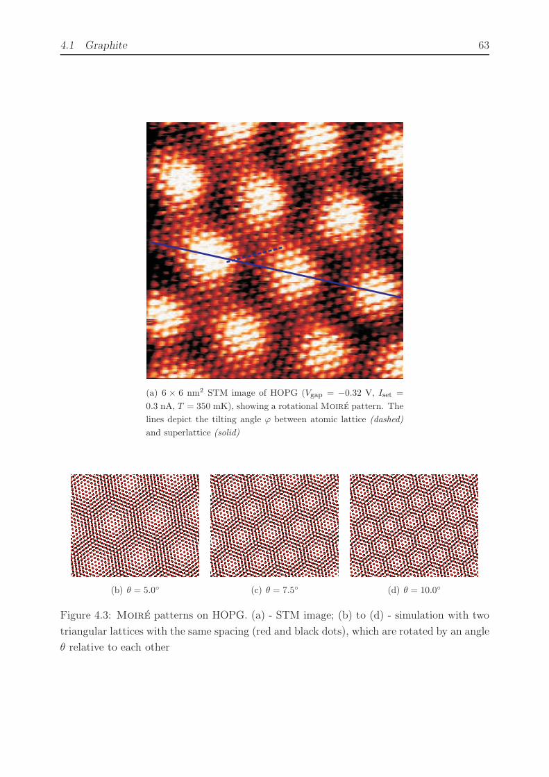
4.1 Graphite 63
(a) 6 × 6 nm2 STM image of HOPG (Vgap = −0.32 V, Iset =
0.3 nA, T = 350 mK), showing a rotational Moire pattern. The
lines depict the tilting angle ϕ between atomic lattice (dashed)
and superlattice (solid)
(b) θ = 5.0 (c) θ = 7.5 (d) θ = 10.0
Figure 4.3: Moire patterns on HOPG. (a) - STM image; (b) to (d) - simulation with two
triangular lattices with the same spacing (red and black dots), which are rotated by an angle
θ relative to each other

64 4 Selected STM Results
-400 -200 0 200 400
dI/d
V (
arb.
uni
ts)
V / mV
-400 0 400
-1
0
1
I / n
A
V / mV
Figure 4.4: Differential conductance dI/dV vs. V of HOPG with a W tip at room temper-
ature. The curve was obtained by numerical differentiation of the I −V curve shown in the
inset. The black line is the calculated total DOS of graphite (Ref. [49])
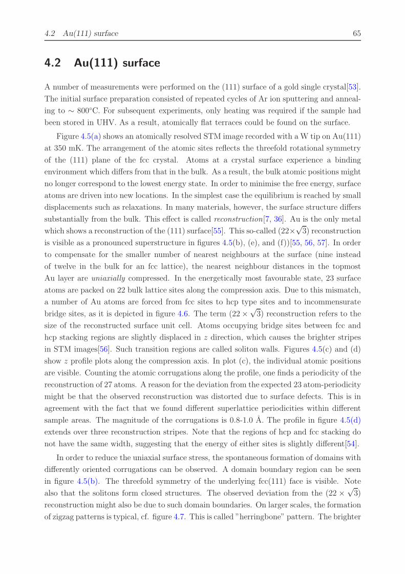
4.2 Au(111) surface 65
4.2 Au(111) surface
A number of measurements were performed on the (111) surface of a gold single crystal[53].
The initial surface preparation consisted of repeated cycles of Ar ion sputtering and anneal-
ing to ∼ 800C. For subsequent experiments, only heating was required if the sample had
been stored in UHV. As a result, atomically flat terraces could be found on the surface.
Figure 4.5(a) shows an atomically resolved STM image recorded with a W tip on Au(111)
at 350 mK. The arrangement of the atomic sites reflects the threefold rotational symmetry
of the (111) plane of the fcc crystal. Atoms at a crystal surface experience a binding
environment which differs from that in the bulk. As a result, the bulk atomic positions might
no longer correspond to the lowest energy state. In order to minimise the free energy, surface
atoms are driven into new locations. In the simplest case the equilibrium is reached by small
displacements such as relaxations. In many materials, however, the surface structure differs
substantially from the bulk. This effect is called reconstruction[7, 36]. Au is the only metal
which shows a reconstruction of the (111) surface[55]. This so-called (22×√
3) reconstruction
is visible as a pronounced superstructure in figures 4.5(b), (e), and (f))[55, 56, 57]. In order
to compensate for the smaller number of nearest neighbours at the surface (nine instead
of twelve in the bulk for an fcc lattice), the nearest neighbour distances in the topmost
Au layer are uniaxially compressed. In the energetically most favourable state, 23 surface
atoms are packed on 22 bulk lattice sites along the compression axis. Due to this mismatch,
a number of Au atoms are forced from fcc sites to hcp type sites and to incommensurate
bridge sites, as it is depicted in figure 4.6. The term (22 ×√
3) reconstruction refers to the
size of the reconstructed surface unit cell. Atoms occupying bridge sites between fcc and
hcp stacking regions are slightly displaced in z direction, which causes the brighter stripes
in STM images[56]. Such transition regions are called soliton walls. Figures 4.5(c) and (d)
show z profile plots along the compression axis. In plot (c), the individual atomic positions
are visible. Counting the atomic corrugations along the profile, one finds a periodicity of the
reconstruction of 27 atoms. A reason for the deviation from the expected 23 atom-periodicity
might be that the observed reconstruction was distorted due to surface defects. This is in
agreement with the fact that we found different superlattice periodicities within different
sample areas. The magnitude of the corrugations is 0.8-1.0 A. The profile in figure 4.5(d)
extends over three reconstruction stripes. Note that the regions of hcp and fcc stacking do
not have the same width, suggesting that the energy of either sites is slightly different[54].
In order to reduce the uniaxial surface stress, the spontaneous formation of domains with
differently oriented corrugations can be observed. A domain boundary region can be seen
in figure 4.5(b). The threefold symmetry of the underlying fcc(111) face is visible. Note
also that the solitons form closed structures. The observed deviation from the (22 ×√
3)
reconstruction might also be due to such domain boundaries. On larger scales, the formation
of zigzag patterns is typical, cf. figure 4.7. This is called ”herringbone” pattern. The brighter

66 4 Selected STM Results
structures in this image result from remainders of contaminants. The darker area indicates
a monoatomic step dividing flat terraces. We used such steps for the z calibration of the
STM piezo drives. The scan profile across the step shown in figure 4.7 indicates a step
height of (2.55 ± 0.10) A, which agrees well with the theoretical value of 2.50 A.
Figure 4.8 shows two images of a gold film which was deposited on a glass substrate by
electron beam evaporation. The surface is much rougher than the single crystal surface.
High resolution images could not be obtained.

4.2 Au(111) surface 67
(a) 6.5 × 6.5nm2; the triangular lattice
refers to the (111) plane of an fcc crystal.
(b) 37 × 37nm2 large scale image, showing
patterns of the surface reconstruction.
0 5 10-80
-40
0
40
80
z / p
m
Lateral distance / nm
(c) Line profile along the compression axis of
the reconstruction in figure (e). The atomic
corrugations are clearly visible
0 5 10 15 20-80
-60
-40
-20
0
20
40
60
80z
/ pm
Lateral distance / nm
(d) Line profile across several reconstruction
stripes in figure (f), showing the magnitude
of the displacement
(e) 12.5×12.5nm2. The height profile along
the line is shown in figure (c).
(f) 20 × 20nm2. The height profile along
the line is shown in figure (d).
Figure 4.5: STM images of the Au(111) surface, showing atomic resolution and surface
reconstruction. Vgap = −0.32 V, Iset = 0.74 nA, T = 350 mK.
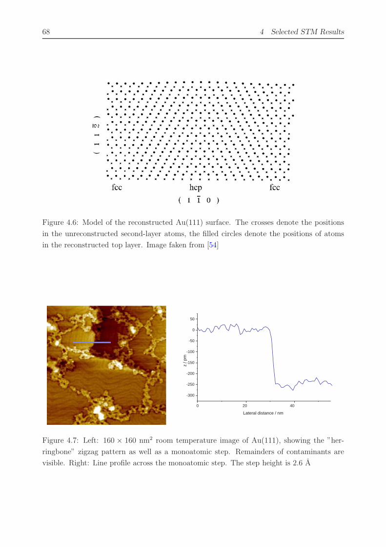
68 4 Selected STM Results
Figure 4.6: Model of the reconstructed Au(111) surface. The crosses denote the positions
in the unreconstructed second-layer atoms, the filled circles denote the positions of atoms
in the reconstructed top layer. Image faken from [54]
0 20 40
-300
-250
-200
-150
-100
-50
0
50
z / p
m
Lateral distance / nm
Figure 4.7: Left: 160 × 160 nm2 room temperature image of Au(111), showing the ”her-
ringbone” zigzag pattern as well as a monoatomic step. Remainders of contaminants are
visible. Right: Line profile across the monoatomic step. The step height is 2.6 A
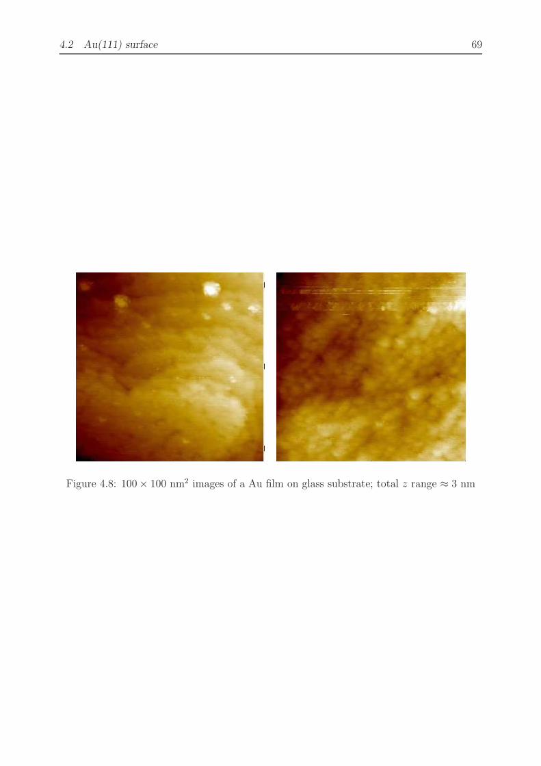
4.2 Au(111) surface 69
Figure 4.8: 100 × 100 nm2 images of a Au film on glass substrate; total z range ≈ 3 nm
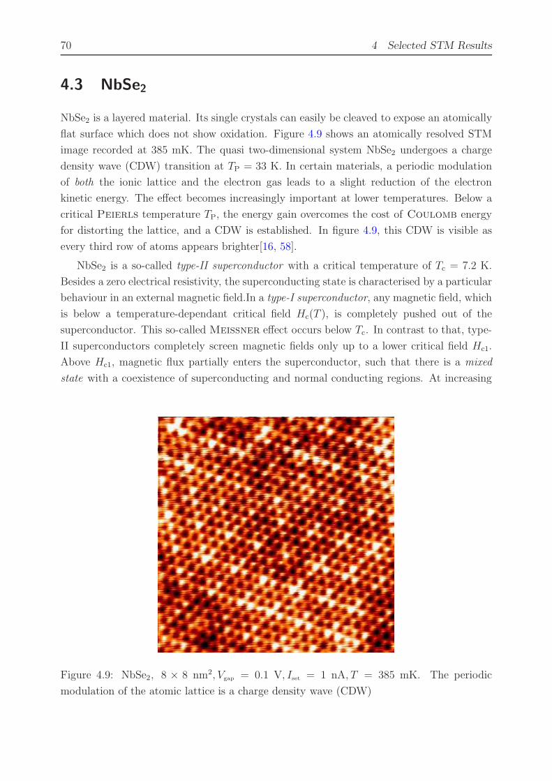
70 4 Selected STM Results
4.3 NbSe2
NbSe2 is a layered material. Its single crystals can easily be cleaved to expose an atomically
flat surface which does not show oxidation. Figure 4.9 shows an atomically resolved STM
image recorded at 385 mK. The quasi two-dimensional system NbSe2 undergoes a charge
density wave (CDW) transition at TP = 33 K. In certain materials, a periodic modulation
of both the ionic lattice and the electron gas leads to a slight reduction of the electron
kinetic energy. The effect becomes increasingly important at lower temperatures. Below a
critical Peierls temperature TP, the energy gain overcomes the cost of Coulomb energy
for distorting the lattice, and a CDW is established. In figure 4.9, this CDW is visible as
every third row of atoms appears brighter[16, 58].
NbSe2 is a so-called type-II superconductor with a critical temperature of Tc = 7.2 K.
Besides a zero electrical resistivity, the superconducting state is characterised by a particular
behaviour in an external magnetic field.In a type-I superconductor, any magnetic field, which
is below a temperature-dependant critical field Hc(T ), is completely pushed out of the
superconductor. This so-called Meissner effect occurs below Tc. In contrast to that, type-
II superconductors completely screen magnetic fields only up to a lower critical field Hc1.
Above Hc1, magnetic flux partially enters the superconductor, such that there is a mixed
state with a coexistence of superconducting and normal conducting regions. At increasing
Figure 4.9: NbSe2, 8 × 8 nm2, Vgap = 0.1 V, Iset = 1 nA, T = 385 mK. The periodic
modulation of the atomic lattice is a charge density wave (CDW)
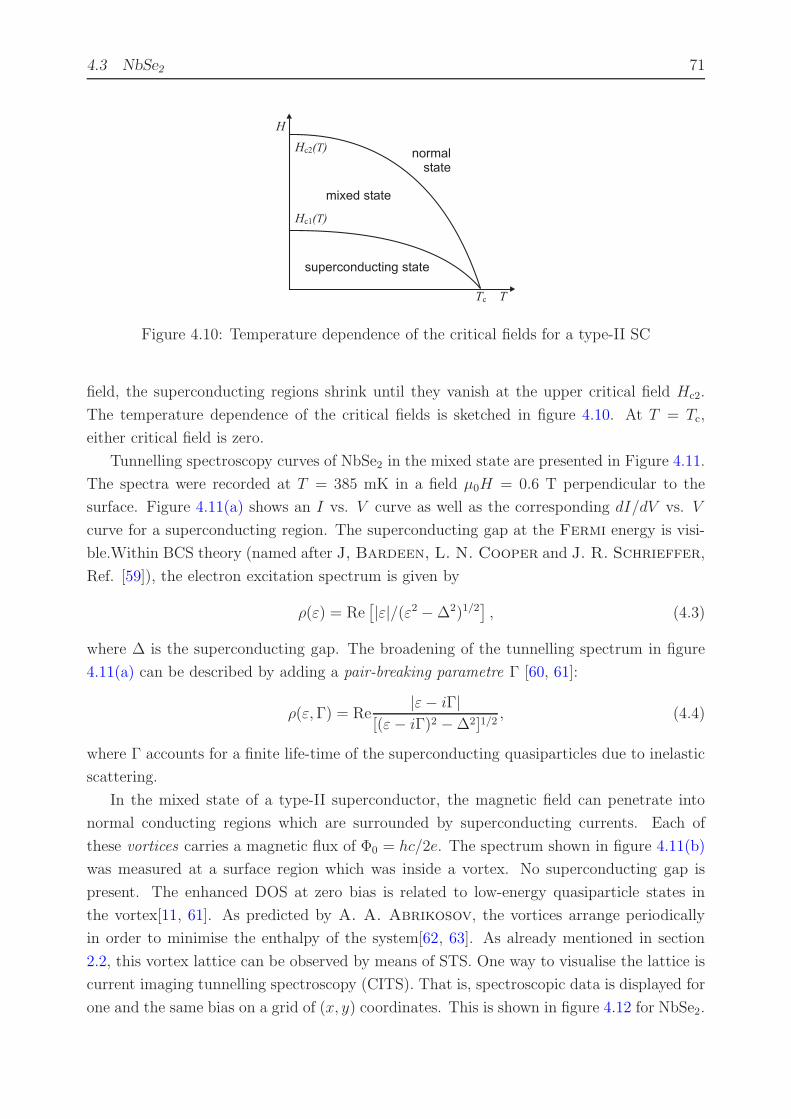
4.3 NbSe2 71
mixed state
H
Tc
Hc2( )T
Hc1( )T
T
normalstate
superconducting state
Figure 4.10: Temperature dependence of the critical fields for a type-II SC
field, the superconducting regions shrink until they vanish at the upper critical field Hc2.
The temperature dependence of the critical fields is sketched in figure 4.10. At T = Tc,
either critical field is zero.
Tunnelling spectroscopy curves of NbSe2 in the mixed state are presented in Figure 4.11.
The spectra were recorded at T = 385 mK in a field µ0H = 0.6 T perpendicular to the
surface. Figure 4.11(a) shows an I vs. V curve as well as the corresponding dI/dV vs. V
curve for a superconducting region. The superconducting gap at the Fermi energy is visi-
ble.Within BCS theory (named after J, Bardeen, L. N. Cooper and J. R. Schrieffer,
Ref. [59]), the electron excitation spectrum is given by
ρ(ε) = Re[
|ε|/(ε2 − ∆2)1/2]
, (4.3)
where ∆ is the superconducting gap. The broadening of the tunnelling spectrum in figure
4.11(a) can be described by adding a pair-breaking parametre Γ [60, 61]:
ρ(ε,Γ) = Re|ε− iΓ|
[(ε− iΓ)2 − ∆2]1/2, (4.4)
where Γ accounts for a finite life-time of the superconducting quasiparticles due to inelastic
scattering.
In the mixed state of a type-II superconductor, the magnetic field can penetrate into
normal conducting regions which are surrounded by superconducting currents. Each of
these vortices carries a magnetic flux of Φ0 = hc/2e. The spectrum shown in figure 4.11(b)
was measured at a surface region which was inside a vortex. No superconducting gap is
present. The enhanced DOS at zero bias is related to low-energy quasiparticle states in
the vortex[11, 61]. As predicted by A. A. Abrikosov, the vortices arrange periodically
in order to minimise the enthalpy of the system[62, 63]. As already mentioned in section
2.2, this vortex lattice can be observed by means of STS. One way to visualise the lattice is
current imaging tunnelling spectroscopy (CITS). That is, spectroscopic data is displayed for
one and the same bias on a grid of (x, y) coordinates. This is shown in figure 4.12 for NbSe2.

72 4 Selected STM Results
The image shows dI/dV at V = 61 µV at T = 385 mK and µ0H = 0.6 T. The brighter spots
result from the enhanced DOS at EF in the vortices as compared to the superconducting
region. The triangular arrangement of the vortices corresponds to literature results[11]. In
order to proof that the bright spots are indeed caused by the vortices, figure shows the
dI/dV curves for different positions, as indicated by the arrow in figure. Going from the
vortex centre towards the SC region, the peak at zero bias is gradually decreasing, and a gap
is opening, whereas the DOS at the gap edge increases accordingly. The measured average
spacing of two vortices av is 67±5 nm. This is in reasonable agreement with the theoretical
value of av = 48.9 nm/√
B[T] = 63.1 nm [11, 64].
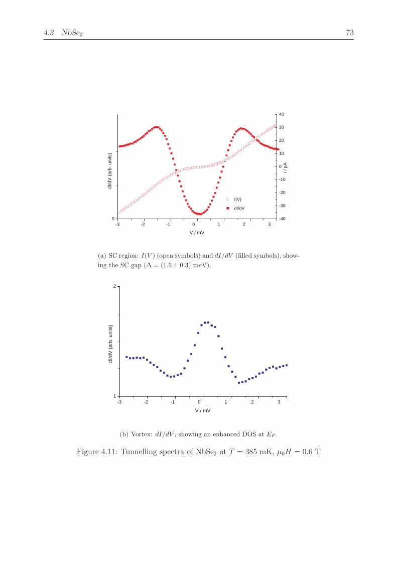
4.3 NbSe2 73
-3 -2 -1 0 1 2 3 0
dI/dV
dI/d
V (
arb.
uni
ts)
V / mV
-40
-30
-20
-10
0
10
20
30
40
I / p
A
I(V)
(a) SC region: I(V ) (open symbols) and dI/dV (filled symbols), show-
ing the SC gap (∆ = (1.5 ± 0.3) meV).
-3 -2 -1 0 1 2 3 1
2
dI/d
V (
arb.
uni
ts)
V / mV
(b) Vortex: dI/dV , showing an enhanced DOS at EF .
Figure 4.11: Tunnelling spectra of NbSe2 at T = 385 mK, µ0H = 0.6 T

74 4 Selected STM Results
(a)
-3 -2 -1 0 1 2 3
dI/d
V (
arb.
uni
ts)
V / mV
(b)
Figure 4.12: (a) 80 × 80 nm2 CITS image of NbSe2 at T = 385 mK, µ0H = 0.5 T, showing
dI/dV at V = 61 µV. The brighter spots originate from the enhanced DOS at EF in a
vortex, and thereby visualise the Abrikosov lattice of the vortices. The arrow indicates
where the sequence of spectra in (b) were recorded. Starting in a vortex (top), the zero-bias
peak disappears and the superconducting gap opens towards the superconducting region.
For clearity, there is an offset of one unit between each two curves. The dashed line marks
the bias V = 61 µV used (a)

5 Summary
The present work deals with the preparation and characterisation of tungsten STM tips as
well as their use in tunnelling experiments. The aim is the reliable manufacture of tips which
perform strongly in STM. Here, the in-situ conditioning of the electrochemically etched tips
takes the centre stage.
Facilities for the conditioning and characterisation of W tips have been implemented
into existing UHV STM systems. This included the design and construction of the stages
themselves as well as providing the technical requirements, such as gas supplies, electric and
electronic equipment, and adequate vacuum conditions. With these technical prerequisites,
it was possible to treat W tips in different ways: annealing by mechanical contact with
a filament and by electron bombardement, and self-sputtering with nonble gas ions. The
efficency of the available metods was investigated in experiments with more than 70 tips.
This does not yet yield sufficiently high statistics to draw irrefutable conclusions about the
ultimate way to prepare tips. However, the results give strong hints as which techniques are
promising to yield good results, and which are appropriate parametres. The main factor
which limits the available amount of data is that the experiments themselves are partially
very time consuming. Only to reach appropriate vacuum conditions takes a lot of time, and
for STM experiments, a lot of patience is inevitable.
In order to determine the quality of the tips and to judge the efficiency of the conditioning
methods, the tips were characterised by means of SEM, field emission and STM experiments.
In numerous cases, the results of the respective methods could be compared and related to
each other. SEM measurements yielded information about the tip shape on a microscopic
scale. In this way, strong contaminations and defects as well as changes to the tip shape
caused by any treatment could be directly visualised. Features on an atomic scale could not
be resolved, though. If more detailed information were needed in future, other experimenal
techniques such as TEM would be required. Field emission is a quick and effective means to
check on the tip sharpness. The main advantage is that the experiments can be carried out in
situ, without removing the tip from the conditioning stage. This makes it particularly useful
to monitor changes to the tip due to some treatment (see, for instance, figure 3.13). It was
proved that the emission indeed occurs from the tip apex, and that the emission current
obeys the Fowler-Nordheim equation. Tip apex radii were extracted from Fowler-
76 5 Summary
Nordheim plots, and the results were in agreement with SEM measurements. Measuring
the threshold voltage required to draw a fixed emission current from the tip was found to
yield a reasonably good estimate of tip sharpness. As a rule of thumb, it was found that the
tip radius in A is roughly 23
of the measured threshold in volts. More experiments would
be necessary to obtain a more exact quantisation. It is doubtful, though, if this would be
profitable for the process of preparing STM tips. It seems that tip sharpness is not the
ultimate criterion for a good tip. In this work, the probability of obtaining good STM
results was highest for tips which, according to field emission, had radii of apex curvature
of about 10 to 15 nm. Apparently, more important than achieving the ultimate sharpness
is it to have tips which are mechanically stable and free of contaminants.
Strong fluctuations of the emission current might be related to the presence of contam-
inants on the tip surface. This would be consistent with the fact that gentle annealing
frequently stabilised the emission current. Furthermore, tips which had been decapitated
during sputtering and can therefore be expected to be free of contaminants, in general
showed very stable field emission after thesputter treatment
In this work, tips were annealed in two different ways: For direct annealing, the tip
shank was brought into contact with a glowing filament wire. If carried out carefully for few
minutes, this procedure was found to be profitable as a first step of conditioning, to remove
water and other volatile contaminants. The major disadvantage is that this method is hardly
controllable. Tips can easily be blunted due to overheating. Better to controll is annealing
by bombardemant with thermionically emitted electrons. It was found that tips are already
affected by fairly low annealing powers because the tips are heated up very locally at the
apex. Increasing the power, the sharpness (as measured by field emission) decreases linearly
due to a dissolution of W and WO3, until a minimum is reached. Heating even stronger,
the tip starts to be gradually blunted. The position of the minimum of sharpness could
so far not be related to properties of the tip. For effective annealing without risking to
blunt the tips, powers of 20 to 100 µW seem to be promising. The success rate in STM of
the tips which had been exclusively treated by electron annealig was rather low (about one
third). The method might be more effective after further optimising the parametres. So
far, most experimants were carried out at voltages of 250 to 500 V. It therefore might be
worthwile sudying the effect of considerably higher voltages, especially since high electric
fields influence the surface diffusion.
More than 30 tips which had been exposed to sputter treatment were tested in STM.
Comparison with SEM data revealed that self sputtering leads to the formation of a head-
and-neck structure (cf. figure 3.16), and eventually to a decapitation of the tip. The latter
is connected to a sudden drop of the sputter voltage. Determinating the sputter process
automatically after such decapitation, the success rate in STM of the resulting tips was
about 60%. Subsequent annealing of the tips further improved this rate. Throughout this
work, self sputtering could only be combined with direct annealing, as described above. It
77
may be worth use electron beam annealing instead. Tips for which no decapitation was
detected generally did not show satisfactory STM results. Crucial for successful sputtering
is sufficiently high vacuum (10−8 mbar range for a neon pressure of 2 to 4 · 10−5 mbar).
Otherwise, the probability to harm the tip by electrical discharges is too high.
In conclusion, the technical prerequisites for tip conditioning have been established, and
the available methods have been tested. Applying one, or a combination of the techniques,
good tips could be prepared with a certain success rate. The quality of the tips was tested
on HOPG, Au(111) and NbSe2 samples, achieving high resolution in topography and spec-
troscopy. A ”recipe” for tip preparation is given in this work. Even though it is specified
for our setups, it may be applicable to other UHV-STM’s, or even to other measurement
techniques which require sharp and clean probes, such as AFM. It shall be noted that this
is not yet the ultimate way to prepare tips. It is rather a basis on which the success rate
can certainly be further improved. Especially, the combination of the above methods with
tip sharpening under the influence of a high electric field, as described in section 3.4.3 seems
to be very promising.

Appendix: A recipe for tip preparation
In the following, a guideline for tip preparation will be given. The procedures are addapted
to the experimental equipment which was available for the present work. Note that this
recipe is not yet claimed to be the ultimate way, further optimisation of certain parametres
may be possible.
Etching (cf. section 3.2)
• Cut pieces of appropriate length from 0.375 mm diameter 5N tungsten wire (VT-STM
6.5-7 mm, Cryogenic STM 10-11 mm). The pliers should be used for this purpose
only. It is profitable to have at least 20 pieces ready.
• Prepare 20 ml of 3M NaOH solution (7.5 ml 32%NaOH solution and 12.5 ml de-ionised
(DI) water), and pour the required quantity into the tip etching stage. During the
whole etching process one should wear gloves to protect the hands from the etchant
and to keep the tips clean.
• Pre-etch the W pieces in order to create a clean and smooth end. For this end, insert
the pieces by 2-3 mm into into the solution, and etch them for about one minute, such
that the W surface becomes shiny and all fibres (originating from the grooves in the
initial wire surface) have come off, but no considerable neck formation is visible yet.
The right point to stop can be seen by observing the etching current: As long as W
fibres stick to the wire, the current fluctuates by several mA. Stop the process when
the current has stabilised and starts to drop gradually. This procedure should be done
at once for all the cut pieces before starting to etch tips. (This is rather tideous work,
but it is worth it...)
• Fill fresh NaOH solution into the beaker of the etching stage. The ring-shaped counter
electrode should not be entirely inserted into the etchant but only touch the surface.
In this way, disturbing H2 gas bubbles are minimised at the tip.
• Immerse a W piece 1.5 mm into the etchant. At the etching power supply, set the
etching voltage to 8.5 V, and the current threshold to =4 mA. If other NaOH concen-
trations are used, the voltage has to be addapted accordingly (∼ 6 V for 4M, ∼ 11V

80 A recipe for tip preparation
for 2M). Focus the optical microscope and set the light source such that the meniscus
around the wire is clearly visible. Put the Plexi-glass shielding around the stage and
start the etching process.
• After two minutes, furter immerse the wire by 0.05-0.1mm, to reduce the sorface
tension at the meniscus. Avoid any vibration at the etching stage.
• After the process was automatically stopped, take the readily etched tip out of the
solution with a pair of tweezers. Rinse the tip carefully a nd thoroughly in DI water.
If the tip is to be used immediately, dry it with clean N2 gas and mount it into the
tip holder. Otherwise store it in ethanol.
• Introduce the tip as quick as possible into the loadlock chamber (FEL, fast entry lock).
While the chamber is opened, leave the N2 gas valve slightly opened, and avoid any
contamination of UHV parts. After closing, start pumping with the turbo pump.
Figure A.1: Recipient and gas supplies of the Cryogenic STM
• For self-sputtering (see below), the gas supply line should be flushed few times: First
open the main Ne valve to allow some gas into the line. Then, after closing the main
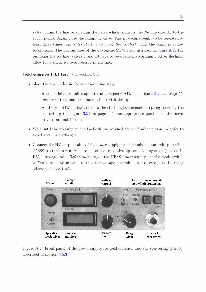
81
valve, pump the line by opening the valve which connects the Ne line directly to the
turbo pump. Again close the pumping valve. This procedure ought to be repeated at
least three times right after starting to pump the loadlock while the pump is at low
revolutions. The gas supplies of the Cryogenic STM are illustrated in figure A.1. For
pumping the Ne line, valves 6 and 10 have to be opened, accordingly. After flushing,
allow for a slight Ne overpressure in the line.
Field emission (FE) test (cf. section 3.3)
• place the tip holder in the corresponding stage:
– Into the left dovetail stage at the Cryogenic STM, cf. figure 3.20 at page 55;
beware of touching the filament loop with the tip
– At the VT-STM, sidewards onto the steel angle, the contact spring touching the
contact leg (cf. figure 3.21 on page 56); the appropriate position of the linear
drive is around 10 mm
• Wait until the pressure in the loadlock has reached the 10−6 mbar region, in order to
avoid vacuum discharges.
• Connect the HV output cable of the power supply for field emission and self-sputtering
(FESS) to the current feedthrough of the respective tip conditioning stage (black=tip
HV, blue=ground). Before swithing on the FESS power supply, set the mode switch
to ”voltage”, and make sure that the voltage controle is set to zero. At the range
selector, choose 1 nA.
Figure A.2: Front panel of the power supply for field emission and self-sputtering (FESS),
described in section 3.5.3
82 A recipe for tip preparation
• CAREFULLY increase the voltage (upper knob), until the current meter shows a
constant value of 1 nA. Note that any change in the applied voltage leads to a charging
of the cable due to its finite capacitance. The displayed current value will therefore
increase by few nA, and then quickly (within ∼ 1 s) drop to the actual current reading.
• If the emission current fluctuates strongly, gently heat the tip (see below) for few
minutes.
• The voltage Vth necessary to draw 1 nA gives an estimate for tip sharpness, cf. section
3.3
– if Vth > 600 V - take a new tip.
– if Vth < 600 V it is worth to continue with conditioning. For low values (up
to 300 V), annealing by electron bombardment (if available) may be sufficient;
otherwise go for Ne self sputtering.
• within the present work, best STM results were obtained with tips which had Vth = 150
to 300 V after treatment, independent of the initial value.
Direct resistive annealing (cf. section 3.4.1)
• This procedure may be applied as a first step of treatment, or subsequently to self-
sputtering (see below).
• Place the tip holder such that the tip shank touches the W filament
– Into the right dovetail stage at the Cryogenic STM. Using a handheld ohmme-
ter, one can check on the contact between tip (tip HV=black) and filament (fil.
voltage=red, or ground=blue)
– At the VT-STM, set the linear drive to 14 mm, and touch the filament, fine-
tuning its position.
• Beware of applying force to the filament, since this might break the brittle W wire.
• Connect an adjustable DC power supply to ’fil. voltage’=red and ground=blue; suit-
able is the power supply for sample heating at the transfer rod (Delta electronics).
• Slowly increase the voltage until the filament begins to glow. The necessary power
depends on the stage and the filament, usual values were V ≈ 1V, I ≈ 2.8A. A too
strong annealing might blunt the tip.
• Note that the resistivity of the filament will further increase as its temperature raises,
leading to an even stronger heating. One should therefore keep an eye on the brightness
of the filament, and reduce the annealing power if necessary.
83
• After few minutes, slowly reduce the voltage to zero, and retract the tip.
Annealing by electron bombardment (not available at the VT-STM)
• At the Cryogenic STM, place the tip in the left dovetail, beneath the looped filament.
Connect the Tectra HV supply[42]: black=tip HV, yellow=filament, blue=ground.
The pressure in the loadlock should be in the 10−7 mbar range or less.
• Measuring the emission current Iemi from the filament is performed as voltage mea-
surement with a handheld voltmeter across a 10 kΩ resistor in series with the output.
That is, a reading of 1 mV corresponds to Iemi = 0.01 µA.
• Tune the voltage VHV to the desired value (e.g. 350 V), and increase the filament cur-
rent Ifil until the filament starts to glow (> 2 A). Keep an eye on the pressure reading:
Due to outgassing may rise drastically due to degassing from the filament. Further
increase Ifil carefully, until Iemi reaches the desired value (usually 0.1 to 1.0 µA).
• Anneal the tip for 30s. Compensate strong fluctuations of Iemi by regulating Ifil.
• Check again on tip sharpness by field emission. If required, repeat annealing with
gradually increased power.
Self sputtering (section 3.4.2)
• For this procedure, an initial tip sharpness is required (FE threshold Vth(I = 1nA) .
600 V).
• The position of the tip is the same as for FE experiments in the respective STM’s.
• The pressure in the loadlock should be in the (lower) 10−8 mbar range, to avoid
discharges. Set the emission of the pressure gauge to 0.1 mA.
• Introduce the sputter gas, preferrably Ne, into the chamber. The gate valve to the
turbo pump should remain opened. In this way, the Ne pressure is better controllable.
By means of the fine leak valve 11, set a pressure of 2..4 · 10−5 mbar.
• Connect the FESS power supply as described above. In addition, make sure the device
is connected to a computer via the USB interface.
• Before switching on the power supply, make sure that both voltage and current control
are set to zero. Set the mode switch to ”current”, the range selector to 1 µA, and
disable the automatic-stop mechanism.
84 A recipe for tip preparation
• With the current control, increase the voltage until the desired emission current (10-
20 µA) is displayed at the current monitor. If the tip is not sharp enough, it will not
be possible to reach these values up to the limit of the sower supply (. 1 kV). In
this case, an emission of a few µA still yields a appreciable sputter rate (it just takes
somewhat longer). For less than 1 µA, one better goes for a new tip.
• When the current is stabilised, enable automatic stopping. If the voltage is fluctuating
strongly, it might be necessary to increase the threshold with the threshold level
control. Typical setting is 25 to 30.
• Start the ”FESS” computer program, and press the ”Start” button. Sputter voltage
as well as emission current are monitored such that changes are visible. The displayed
voltage Uc is corrected by the effect of the internal output resistance of the power
supply (10.88 MΩ).
• The sputter process can be interrupted by the ”Stop” and ”Start” buttons at the
FESS power supply.
• Over time, the sputter voltage Vs should decrease gradually. However, it does not
necessarily drop monotonously.
• After some time, the process is automatically terminated due to a jump in voltage. In
order to check if the detected jump was indeed due to a decapitation of the tip (and
not only due to some fluctuation of the signal), it is useful to perform a FE test. For
this it is recommended to close the Ne gas inlet valve. The FE threshold for 1 nA
should be lower than about 2/3 of Vs for an emission of 10 µA just before the voltage
drop (this is just a rule of thumb based on experience). Another hint is the shape of
the Vs vs t curve. Normally, one can observe a reduction of the noise, and a slight
down-turn (both can be seen in figure 3.15 on page 47).
• After self-sputtering, it strongly recommended to gently anneal the tip, in order to
cure demages at the tip apex due to the sputter treatment.
Bibliography
[1] R. Wiesendanger and H.-J. Guntherodt, editors. Scanning Tunneling Microscopy III,
volume 29 of Springer Series in Surface Sciences. Springer, 2nd edition, 1996. 15, 18,
88
[2] G. Binning and H. Rohrer. Scanning tunneling microscopy. Helv. Phys. Acta, 55:726–
735, 1982. 16
[3] J. Bardeen. Tunneling from a many-particle point of view. Physical Review Letters,
6(2):57–59, 1961. 16
[4] J. Tersoff and D. R. Hamann. Theory of the scanning tunneling microscope. Physical
Review B, 31(2):805–813, 1985. 16
[5] L. Pauling and E. B. Wilson, Jr. Introduction to Quantum Mechanics, chapter 27b,
pages 198–201. Reprint by Dover Publications Inc., New York, 1985. 17
[6] R. J. Hamers. Methods of Tunnelling Spectroscopy with the STM, chapter 4, pages
51–103. In Bonnell [65], 1993. 17, 18
[7] W. Unertl. The Surface Structure of Crystalline Solids, chapter 5, pages 107–154. In
Bonnell [65], 1993. 21, 65
[8] Omicron NanoTechnology GmbH, 65232 Taunusstein, Germany. 21, 33
[9] Oxford Instruments Ltd., Abingdon Oxfordshire, OX13 5QX, UK. 24
[10] F. Pobell. Matter and Methods at Low Temperatures. Springer Verlag, 2nd edition,
1996. 27
[11] H. F. Hess, R. B. Robinson, R. C. Dynes, J. M. Valles Jr., and J. V. Waszczak. Scanning-
Tunneling-Microscope Observation of the Abrikosov Flux Lattice and the Density of
States near and inside a Fluxoid. Physical Review Letters, 62(2):214–216, 1989. 27, 71,
72
86 BIBLIOGRAPHY
[12] H. Rohrer. The Preparation of Tips and Sample Surfaces for STM Experiments, chap-
ter 6, pages 155–187. In Bonnell [65], 1993. 29, 30, 31
[13] I. Ekvall, E. Wahlstrom, D. Claesson, H. Olin, and E. Olsson. Preparation and charak-
terization of electrochemically etched W tips for STM. Meas. Sci. Technol., 10:11–18,
1999. 29, 31, 42, 43, 44, 46, 48
[14] H. Neddermeyer and M. Drechsler. Electric field-induced changes of W(110) and
W(111) tips. Journal of Microscopy, 152:459–466, August 1988. 30, 53
[15] J. G. Rodrigo, H.Suderow, and S. Vieira. On the use of STM superconducting tips at
very low temperatures. European Physics Journal B, 40:483–488, 2004. 30
[16] S. H. Pan and E. W. Hudson and J. C. Davis. Vacuum tunneling of superconduct-
ing quasiparticles from atomically sharp scanning tunneling microscope tips. Applied
Physics Letters, 73(20):2992–2994, 1998. 30, 70
[17] Santos F. Alvarado and Philippe Renaud. Observation of spin-polarized-electron tun-
neling from a ferromagnet into GaAs. Physical Review Letters, 68:1387–1390, 1992.
30
[18] R. Wiesendanger, D. Burgler, G. Tarrach, A. Wadas, D. Brodbeck, H.-J. Guntherod,
G. Guntherodt, R. J. Gambino, and R. Ruf. Vacuum tunneling of spin-polarized elec-
trons detected by scanning tunneling microscopy. Journal of Vacuum Science and
Technology, 9:519–524, 1991. 30
[19] A. Kubetzka, M. Bode, O. Pietzsch, R. Wiesendanger. Spin-polarized scanning tunnel-
ing microscopy with antiferromagnetic probe tips. Physical Review Letters, 88:057201,
2002. 30
[20] H. Ness and F. Gautier. The electronic structure and stability of transition metal
nanotips - part I. Journal of Physics: Condensed Matter, 7:6625–6640, 1995. 31
[21] H.-W. Fink. Mono-atomic tips for scanning tunneling microscopy. IBM Journal of
Research and Development, 30(5):460–465, 1986. 31, 53
[22] Vu Thien Binh. In situ fabrication and regeneration of microtips for scanning tunneling
microscopy. Journal of Microscopy, 152:355–361, August 1988. 31, 42, 44
[23] O. Albrektsen, H. W. M. Salemink, K. A. Mørch, and A. R. Tholen. Relieable tip
preparation tor high-resolution scanning tunneling microscopy. Journal of Vacuum
Sciences and Technology, 12(6):3187–3190, 1994. 31, 46, 48
[24] Goodfellow Cambridge Ltd., Huntingdon, PE29 6WR, UK. 31
BIBLIOGRAPHY 87
[25] A.-S. Lucier, Henrik Mortensen, Yan Sun, and Peter Gruttner. Determination of the
atomic structure of scanning probe microscopy tungsten tips by field ion microscopy.
Physical Review B, 72:235420, 2005. 31
[26] R. Zhang and D. G. Ivey. Preparation of sharp polycrystalline tungsten tips for scanning
tunneling microscopy imaging. Journal of Vacuum Science and Technology B, 14(1):1–
10, 1996. 32, 33
[27] J. P. Ibe, P. P. Bey Jr., S. L. Brandow, R. A. Brizzolara, N. A. Burnham, D. P.
DiLella, K. P. Lee, C. R. K. Marrian, and R. J. Colton. On the electrochemical etching
of tips for scannin tunneling microscopy. Journal of Vacuum Science and Technology
A, 8(4):3570, 1990. 32, 34, 42
[28] C. Bai. Scanning Tunneling Microscopy and its Application, volume 32 of Springer
Series in Surface Sciences. Springer, 1995. 32
[29] A.-S-Lucier. Preparation and Characterization of Tungsten Tips Suitable for Molecular
Electronics Studies. Master’s thesis, Center for the Physics of Materials Department
of Physics McGill University Montreal, Quebec Canada, 2004. 32, 36, 37, 42
[30] R. H. Fowler and L. Nordheim. Field Emission in Intense Electric Fields. Proceedings
of the Royal Society of London, Series A, 119:173, 1928. 36
[31] L. Nordheim. The Effect of the Image Force on the Emission and Reflection of Electrons
by Metals. Proceedings of the Royal Society of London, Series A, 121:626, 1928. 36, 39
[32] A. Modinos. Field, thermionic, and secondary electron emission spectroscopy. Plenum
Press, 1984. 36
[33] A. P. Jansen and J. P. Jones. The sharpening of field emitter tips by ion sputtering.
Journal of Physics D: Applied Physics, 4:118–123, 1970. 36, 37, 46, 49
[34] G. J. de Raad, P. M. Koenraad, and J. H. Wolter. Use of the Schiller decapitation
process for the manufacture of high quality tungsten scanning tunneling microscopy
tips. Journal of Vacuum Sciences and Technology, 17(5):1946–1952, 1999. 40, 42, 47,
49
[35] L. Ottaviano, L. Lozzi, and S. Santucci. Scanning Auger microscopy study of W tips
for scanning tunneling microscopy. Review of Scientific Instruments, 74(7):3368–3378,
2003. 42
[36] Ch. Kittel. Einfuhrung in die Feskorperphysik. Oldenbourg, 7th edition, 1988. 44, 65
88 BIBLIOGRAPHY
[37] C. Schiller, A. A. Koomans, T. L. van Rooy, C. Schonenberger, and H. L. van Elswijk.
Decapitation of tungsten field emitter tips during sputter sharpening. Surface Science,
339:L925–L930, 1995. 46, 48, 49
[38] J. Y. Cavaille and M. Drechsler. Ion impact on fieldemitter crystals. Revue de Physique
Appliqee, 12:1631–1639, October 1977. 47, 49
[39] H. Vogel. Gerthsen Physik. Springer, 19th edition, 1997. 53
[40] W. Nolting. Grundkurs Theoretische Physik 3: Elektrodynamik. Springer, 6th edition,
2002. 53
[41] Ch. Renner. private conversation. 53
[42] tectra GmbH, 60323 Frankfurt/M, Germany. 55, 83
[43] Conrad Electronics GmbH, 92240 Hirschau, Germany. 57
[44] R. Wiesendanger and D. Anselmetti. STM on Layered Materials, chapter 6, pages
131–179. Volume 20 of R. Wiesendanger and H.-J. Guntherodt [66], 2nd edition, 1994.
60
[45] M. Tsukada, K. Kobayashi, N. Isshiki, S. Watanabe, H. Kageshima, and T. Schimizu.
The Role of Tip Atomic and Electronic Structure in Scanning Tunneling Microscopy
and Spectroscopy, chapter 5, pages 77–103. Volume 29 of Wiesendanger and Guntherodt
[1], 2nd edition, 1996. 60
[46] Z. Y. Rong and P. Kuiper. Electronic effects in scanning tunneling microscopy: Moire
pattern on a graphite surface. Physical Review B, 48(23):17427–17431, 1993. 60, 61
[47] T. R. Albrecht, H. A. Mizes, J. Nogami, Sang il Park, and C. F. Quate. Observation of
tilt boundaries in graphite by scanning tunneling microscopy and associated multiple
tip effects. Applied Physics Letters, 52(5):362–364, 1987. 60
[48] M. Kuwabara, D. R. Clarke, and D. A. Smith. Anomalous superperiodicity in scanning
tunneling microscope images on graphite. Applied Physics Letters, 56(24):2396–2398,
1990. 61
[49] J. W. McClure. Band Structure of Graphite and de Haas-van Alphen Effect. Physical
Review, 108(3):612–618, 1957. 61, 64
[50] S. Reich, J. Maultzsch, and C. Thomsen. Tight-binding description of graphene. Phys-
ical Review B, 66:035412, 2002. 61
BIBLIOGRAPHY 89
[51] H. Bross and W. Alsheimer. Electronic Structure of Graphite. Reports on the Research
Projects on the High Performance Computers of the Leibnitz Computing Centre of the
Bavarian Academy of Sciences and Humanities 1997-1999, pages 374–376. 61
[52] S. Y. Zhou, G.-H. Gweon, C. D. Spataru, J. Graf, D.-H. Lee, Steven G. Louie, and
A. Lanzara. Coexistence of Sharp Quasiparticle Dispersions and Disorder Features in
Graphite. Physical Review B, 71:161403, 2005. 61
[53] MaTecK Material-Technologie & Kristalle GmbH, D-52428 Julich, Germany. 65
[54] N. Takeuchi, C. T. Chan, and K. M. Ho. Au(111): A theoretical study of the surface
reconstruction and the surface electronic state. Physical Review B, 43(17):13899–13905,
1991. 65, 68
[55] W. Haiss, D. Lackley, J. K. Sass, and K. H. Besocke. Atomic resolution scanning
tunneling microscopy images of Au(111) surfaces in air and polar organic solvents.
Journal of Chemical Physics, 95(3):2193–2196, 1991. 65
[56] Ch. Woll, S. Chiang, R. J. Wilson, and P. H. Lippel. Determination of atom positions
at stacking-fault dislocations on Au(111) by scanning tunneling microscopy. Physical
Review B, 39:7988–7991, 1989. 65
[57] J. V. Barth, H. Brune, G. Ertl, and R. J. Brehm. Scanning tunneling microscopy
observations on the reconstructed Au(111) surface: Atomic structure, long-range su-
perstructure, rotational domains, and surface defects. Physical Review B, 42:9307–9318,
1990. 65
[58] B. Giambattista, A. Johnson, R. V. Coleman, B. Drake, and P. K. Hansma. Charge-
density waves observed at 4.2 K by scanning-tunneling microscopy. Physical Review B,
37(5):2741–2744, Feb 1988. 70
[59] J. Bardeen, L. N. Cooper, and J. R. Schrieffer. Theory of Superconductivity. Physical
Review, 108(5):1175–1204, 1957. 71
[60] R. C. Dynes, V. Narayanamurti, and J. P. Garno. Direct Measurement of Quasiparticle-
Lifetime Broadening in a Strong-Coupled Superconductor. Physical Review Letters,
41(21):1509–1512, 1978. 71
[61] Ch. Renner, A. D. Kent, Ph. Niedermann, Ø. Fischer, and F. Levy. Scanning Tunneling
Spectroscopy of a Vortex Core from the Clean to the Dirty Limit. Physical Review
Letters, 67(12):1650–1652, 1991. 71
[62] A. A. Abrikosov. On the Magnetic Properties of Superconductors of the Second Group.
Soviet Physics JETP, 5(6):1174–1182, 1957. 71
90 BIBLIOGRAPHY
[63] U. Essmann and H. Trauble. The direct observation of individual flux lines in type II
superconductors. Physics Letters, 24A(10):526–527, 1967. 71
[64] S. Behler, S. H. Pan, P. Jess, A. Baratoff, H.-J. Guntherodt, F. Levy, G. Wirth, and
J. Wiesner. Vortex Pinning in Ion-Irradiated NbSe2 Studied by Scanning Tunneling
Microscopy. Physical Review Letters, 72(11):1750–1752, 1993. 72
[65] D. A. Bonnell, editor. Scanning Tunneling Microscopy and Spectroscopy: Theory, Tech-
niques and Applications. VCH Publishers, Inc., 1993. 85, 86
[66] R. Wiesendanger and H.-J. Guntherodt, editors. Scanning Tunneling Microscopy I,
volume 20 of Springer Series in Surface Sciences. Springer, 2nd edition, 1994. 88

Acknowledgements
I would like to express my gratitude to all those persons from which I received support
throughout the work for this thesis.
First and foremost, I thank Prof. Frank Steglich for his support in many respects, particu-
laly for the opportunity to complete my Diploma in such a unique working environment.
Specifically grateful I am to Steffen Wirth, who succeded to give me excellent supervision
during my work, even in turbulent times. I felt to have a lot of freedom to work individ-
ually, while never being alone ”out on a limb”. Particularly important were our numerous
discussions and his helpful comments to this thesis.
Throughout the first part of my work I had the pleasure to cooperate with Michal Rams. I
gratefully acknowledge his numerous contributions to this work, specifically concerning the
electronics and software programming, and I enjoyed our fruitful and friendly discussions,
whether they were about physics or not.
Furthermore, I would like to thank Sahana Roßler and Voicu Dolocan for the numerous
discussions and the many helpful comments and proposals for corrections to this work.
The scanning electron microscopy data provided by Mrs. Petra Scheppan (in the groups of
Rainer Ramlau and Ulrich Burkhard) make up an important part of this thesis. I appreci-
ated the friendly and uncomplicated cooperation.
A number of technical problems which occured during this work could be solved with sup-
port of the mechanical workshop and the electronics workshop of our institute.
Peter Kes I thank for providing the NbSe2 sample which was used during my work.
Finally, I feel this is the right occasion to also express my heartfelt gratitude to my family,
my parents in particular, who supported me in many ways throughout my physics studies.
I also thank Ina for her patience and support during the time of writing-up.


Erklarung
Hiermit bestatige ich, dass ich diese Diplomarbeit ohne unzulassige Hilfe Dritter und ohne
die Benutzung anderer als der angegebenen Hilfsmittel angefertigt habe. Die aus fremden
Quellen direkt oder indirekt ubernommenen Gedanken sind als solche kenntlich gemacht.
Die Arbeit wurde bisher weder im Inland noch im Ausland in gleicher oder ahnlicher Form
einer anderen Prufungsbehorde vorgelegt.
Stefan Ernst Dresden, 26. Juni 2006