Embed Size (px)
Citation preview
Optimization of Analog Circuitsby Applying Evolutionary
Algorithms
by
Ivick Guerra Gomez
A DissertationSubmitted to the Program in Electronics Science,
Electronics Science Departmentin partial fulfillment of the requirements for the degree of
PH.D. IN ELECTRONICS SCIENCE
at the
National Institute for Astrophysics, Optics and ElectronicsJuly 2012
Tonantzintla, Puebla
Advisors:
Dr. Esteban Tlelo Cuautle, INAOE.Dr. Trent McConaghy, Solido Design Automation Inc.
c⃝INAOE 2012All rights reserved
The author hereby grants to INAOE permission to reproduce andto distribute copies of this thesis document in whole or in part

To Leonor, Dafne and Sofía
Abstract
Unlike automated digital design, analog circuit designers require experience to develop skills,
and to avoid spending a lot of time understanding all the aspects involved around a specific
design such as nonlinearities, parasitics, performances, trade-offs, etc.
The continuing size reduction of electronic devices along with their shorter life cycle im-
poses design challenges to discover or to optimize the performances of modern electronic sys-
tems; such as: wireless services, telecom, mobile computing and media applications. Fortu-
nately, those design challenges can be overcome through the development of Electronic Design
Automation (EDA) tools.
In the analog domain, circuit optimization tools have demonstrated their usefulness in ad-
dressing design problems taking into account downscaling technological aspects. However,
those EDA tools still have the lack of taking into account some design constraints when applied
to a multiple objective design problem.
On the one hand, Evolutionary Algorithms (EAs) have demonstrated their suitability in
solving nonlinear multi-objective design problems with multiple constraints, providing a set of
feasible design solutions from which several insights and trade-offs among the circuit perfor-
mance objectives can be deduced. On the other hand, still the application of EAs in optimizing
the biases and sizes of analog circuits, have hard shortcomings to be improved, for instance:
guarantee of convergence, run-time and incorporation of variation aware techniques.
This Thesis is focused on the application of multi-objective EAs in the optimization of ana-
log circuits including nanometer technology. The EAs have been programmed to work with
different genetic operators over different kinds of circuit objectives, variables and design tech-
nologies. A major contribution is presented by introducing an automatic current-bias distribu-
i

ii
tion to accelerate convergence of the EAs in optimizing analog circuits. Another contribution is
introduced through the implementation of a procedure oriented to compute process variations
while diminishing the number of simulations. That is, optimal solutions are found by adapting
a simulation budget allocation procedure to efficiently distribute the number of simulations. Fi-
nally, this Thesis includes an appendix to describe an EDA tool based on EAs for biasing and
sizing analog circuits and taking into account process variations issues.

Resumen
A diferencia del diseno digital automatizado, los disenadores de circuitos analogicos requieren
experiencia para desarrollar habilidades y ası evitar desperdiciar tiempo en entender todos los
aspectos que estan involucrados alrededor de un diseno especıfico, como es el caso de las no-
linealidades, efectos parasitos, rendimiento del circuito, compromisos de diseno, etc.
La continua reduccion del tamano de los dispositivos electronicos aunado a su ciclo de
vida cada vez menor, imponen retos de diseno para descubrir u optimizar el rendimiento de los
sistemas electronicos modernos. Tal es el caso de sistemas inalambricos, telecomunicaciones,
dispositivos portatiles y aplicaciones multimedia. Afortunadamente, dichos retos de diseno
pueden superarse a traves del desarrollo de herramientas de Diseno Electronico Automatizado
(EDA).
En el dominio analogico, las herramientas para la optimizacion de circuitos han demostrado
una gran utilidad para abordar los problemas de diseno tomando en cuenta los aspectos de
escalamiento tecnologico. Sin embargo, estas herramientas de EDA aun presentan deficiencias
al tomar en cuenta algunos compromisos de diseno cuando se aplican a un problema de diseno
multi-objetivo.
Por una parte, los Algoritmos Evolutivos (EAs) han demostrado ser idoneos para resolver
problemas de diseno nolineales multi-objetivo con multiples compromisos, aportando un con-
junto de soluciones factibles. A partir de este conjunto de soluciones se pueden hacer algunas
conjeturas para establecer relaciones entre los diferentes rendimientos de un circuito. Por otra
parte, la aplicacion de EAs en la optimizacion a base del dimensionamiento y polarizacion de
circuitos analogicos, aun tiene muchos inconvenientes que deben ser superados, por ejemplo:
garantizar la convergencia, el tiempo de computo y la incorporacion de tecnicas que tomen en
iii

iv
cuenta las variaciones de proceso.
Esta Tesis esta enfocada a la aplicacion de EAs multi-objetivo en la optimizacion de cir-
cuitos analogicos de tecnologıas nanometricas. Los EAs han sido programados para trabajar
con diferentes operadores geneticos , diferentes tipos de objetivos de circuito, varias variables
y distintas tecnologıas de diseno. Se presenta una contribucion al introducir una distribucion
de corrientes de polarizacion automaticamente para acelerar la convergencia de los EAs en
la optimizacion de circuitos analogicos. Tambien se presenta otra contribucion a traves de la
implementacion de un procedimiento para calcular las variaciones de proceso con un numero
menor de simulaciones.
Finalmente, esta Tesis incluye un apendice donde se describe una herramienta EDA basada
en EAs para la polarizacion y dimensionamiento de circuitos analogicos tomando en cuenta las
variaciones de proceso.
Publications
Papers
• I. Guerra-Gomez, E. Tlelo-Cuautle, T. McConaghy, and G. Gielen, “Decomposition-
Based Multi-Objective Optimization of Second-Generation Current Conveyors,” IEEE
International Midwest Symposium on Circuits and Systems, pp. 220–223, August 2009.
• I. Guerra-Gomez, E. Tlelo-Cuautle, G. Reyes-Salgado, and Luis G. de la Fraga, “Non-
sorting genetic algorithm in the optimization of unity-gain cells,” International Confer-
ence on Electrical Engineering, Computing Science and Automatic Control, pp. 445–450,
Toluca-Mexico, November 2009.
• I. Guerra-Gomez, E. Tlelo-Cuautle, T. McConaghy, and G. Gielen, “Optimizing Cur-
rent Conveyors by Evolutionary Algorithms Including Differential Evolution,” Interna-
tional Conference on Electronics Circuits and Systems, Special Session, pp. 259–262,
Hammamet-Tunisia, December 2009.
• E. Tlelo-Cuautle, I. Guerra-Gomez, M. A. Duarte-Villasenor, Luis G. de la Fraga, G.
Flores-Becerra, G. Reyes-Salgado, C.A. Reyes-Garcıa and G. Reyes-Gomez, “Applica-
tions of Evolutionary Algorithms in the Design Automation of Analog Integrated Cir-
cuits,” Journal of Applied Sciences, vol. 10, no. 17, pp. 1859–1872, 2010.
• I. Guerra-Gomez, E. Tlelo-Cuautle, T. McConaghy, Luis G. de la Fraga and G. Gielen,
“Sizing mixed-mode circuits by multi-objective evolutionary algorithms,” IEEE Interna-
tional Midwest Symposium on Circuits and Systems, pp. 813–816, August 2010.
v
vi
• I. Guerra-Gomez, E. Tlelo-Cuautle and Luis G. de la Fraga, “Sensitivity analysis in
the Optimal Sizing of Analog Circuits by Evolutive Algorithms,” International Confer-
ence on Electrical Engineering, Computing Science and Automatic Control, pp. 381–385,
Chiapas-Mexico, September 2010.
• A. Sallem, I. Guerra-Gomez, M. Fakhfakh, M. Loulou, E. Tlelo-Cuautle, “Simulation-
Based Optimization of CCIIs Performances in Weak Inversion,” International Conference
on Electronics Circuits and Systems, pp. 661–664, Athens-Greece, December 2010.
• S. Polanco-Martagon, G. Reyes-Salgado, G. Flores-Becerra, I. Guerra-Gomez, E. Tlelo-
Cuautle, L. Gerardo de la Fraga, M.A. Duarte-Villasenor, Selection of MOSFET Sizes
by Fuzzy Sets Intersection in the Feasible Solutions Space, Journal of Applied Research
and Technology, vol. 10, no. 3, pp. 472-483, 2012.
Book Chapters.
• E. Tlelo-Cuautle, I. Guerra-Gomez, C. A. Reyes-Garcıa, and M. A. Duarte-Villasenor,
Intelligent Systems for Automated Learning and Adaptation: Emerging Trends and Ap-
plications, ch. 8: Synthesis of Analog Circuits by Genetic Algorithms and their Opti-
mization by Particle Swarm Optimization, IGI Global, pp. 173–192, 2010.
• E. Tlelo-Cuautle, I. Guerra-Gomez, Luis G. de la Fraga, G. Flores-Becerra, S. Polanco
Martagon, M. Fakhfakh, C.A. Reyes-Garcıa , G. Reyes-Gomez and G. Reyes-Salgado,
Intelligent Computational Optimization in Engineering ch. Evolutionary Algorithms in
the Optimal Sizing of Analog Circuits, Springer, pp. 110-138, 2011.
• I. Guerra-Gomez, M.A. Duarte-Villasenor, E. Tlelo-Cuautle, Luis G. de la Fraga, Analy-
sis, Design and Optimization of Active Devices, in Integrated Circuits for Analog Signal
Processing, ISBN: 978-1-4614-1382-0, Springer, June 2012.

Acknowledgements
This work is dedicated to my family whom have supported me always. Also, my most sincere
gratitude for the guidance of my advisors, Dr. Esteban Tlelo Cuautle and Trent McConaghy.
I want also thank Dr. Francisco Fernandez, Dr. Gerardo de la Fraga, Dr. Gustavo
Rodrıguez, Dr. Guillermo Espinosa and Dr. Arturo Sarmiento for their advices and taking
part of my thesis work.
Finally is my appreciation to the Instituto Nacional de Astrofısica, Optica y Electronica
(INAOE) and the Consejo Nacional de Ciencia y Tecnologıa (CONACyT) for its support through
the scholarship 27516/204240 and the projects 131839-Y and 48396-Y.
vii

viii
Contents
Abstract i
Resumen iii
Publications v
Acknowledgements vii
1 Introduction 1
1.1 Analog Circuit Optimization Tools: Categories and Classifications . . . . . . . . 2
1.2 EDA tools . . . . . . . . . . . . . . . . . . . . . . . . . . . . . . . . . . . . . . . . 4
1.3 Justification . . . . . . . . . . . . . . . . . . . . . . . . . . . . . . . . . . . . . . . 8
1.4 Objectives . . . . . . . . . . . . . . . . . . . . . . . . . . . . . . . . . . . . . . . . 10
1.5 Thesis Organization . . . . . . . . . . . . . . . . . . . . . . . . . . . . . . . . . . 12
2 Evolutionary Algorithms 15
2.1 Introduction . . . . . . . . . . . . . . . . . . . . . . . . . . . . . . . . . . . . . . . 15
2.2 Evolutionary Algorithms concepts . . . . . . . . . . . . . . . . . . . . . . . . . . 15
2.2.1 Individuals, Population, Evolutionary Operators and Objective Function 15
2.2.2 The General Evolutionary Algorithm . . . . . . . . . . . . . . . . . . . . 17
2.3 Multiobjective Optimization and Pareto Dominance . . . . . . . . . . . . . . . . 18
2.3.1 Multiobjective Design Problem . . . . . . . . . . . . . . . . . . . . . . . 18
2.3.2 Pareto Dominance . . . . . . . . . . . . . . . . . . . . . . . . . . . . . . . 19
2.3.3 Diversity and Efficiency . . . . . . . . . . . . . . . . . . . . . . . . . . . 20
ix
x CONTENTS
2.4 Genetic Operators . . . . . . . . . . . . . . . . . . . . . . . . . . . . . . . . . . . . 21
2.4.1 Crossover and Mutation . . . . . . . . . . . . . . . . . . . . . . . . . . . . 21
2.4.2 Differential Evolution (DE) . . . . . . . . . . . . . . . . . . . . . . . . . 22
2.4.3 Simulated Binary Cross-Over Operator (SBX) . . . . . . . . . . . . . . . 22
2.4.4 Polynomial Mutation . . . . . . . . . . . . . . . . . . . . . . . . . . . . . 23
2.5 NSGA-II, MOEAD and MOPSO . . . . . . . . . . . . . . . . . . . . . . . . . . . 24
2.5.1 Non-Dominated Sorting Genetic Algorithm II (NSGA-II) . . . . . . . . 24
2.5.2 Multi-Objective Evolutionary Algorithm based on Decomposition (MOEAD) 27
2.5.3 Multi-Objective Particle Swarm Optimization (MOPSO) . . . . . . . . . 29
2.5.4 Behavior of NSGA-II, MOEAD and MOPSO on test functions ZDT . . 31
2.6 Summary . . . . . . . . . . . . . . . . . . . . . . . . . . . . . . . . . . . . . . . . 33
3 Circuit Optimization 37
3.1 Introduction . . . . . . . . . . . . . . . . . . . . . . . . . . . . . . . . . . . . . . . 37
3.2 Optimization Methodology Framework . . . . . . . . . . . . . . . . . . . . . . . 37
3.3 Circuit Optimization with SBX and DE . . . . . . . . . . . . . . . . . . . . . . . 39
3.3.1 Multi-Objective Optimization Problem Formulation . . . . . . . . . . . . 39
3.3.2 Results . . . . . . . . . . . . . . . . . . . . . . . . . . . . . . . . . . . . . 41
3.4 Circuit Optimization with NSGA-II, MOEAD and MOPSO . . . . . . . . . . . . 47
3.4.1 Multi-Objective Optimization Problem Formulation . . . . . . . . . . . . 49
3.4.2 Results . . . . . . . . . . . . . . . . . . . . . . . . . . . . . . . . . . . . . 52
3.5 Summary . . . . . . . . . . . . . . . . . . . . . . . . . . . . . . . . . . . . . . . . 57
4 Automatic current-bias distribution 59
4.1 Introduction . . . . . . . . . . . . . . . . . . . . . . . . . . . . . . . . . . . . . . . 59
4.2 Bias assignments in CMOS analog circuits by graph manipulations . . . . . . . 59
4.3 Modeling the Transistor for Current Bias Partitioning . . . . . . . . . . . . . . . 62
4.3.1 Modeling the Transistor . . . . . . . . . . . . . . . . . . . . . . . . . . . . 62
4.3.2 Current Bias Distribution . . . . . . . . . . . . . . . . . . . . . . . . . . . 63
4.4 Circuits and graphs . . . . . . . . . . . . . . . . . . . . . . . . . . . . . . . . . . . 64
CONTENTS xi
4.4.1 Incidence Matrix . . . . . . . . . . . . . . . . . . . . . . . . . . . . . . . . 64
4.4.2 Depth First Search for biasing . . . . . . . . . . . . . . . . . . . . . . . . 65
4.5 Proposed Current-Branches-Bias Assignment (CBBA) Approach . . . . . . . . . 67
4.6 Application Examples . . . . . . . . . . . . . . . . . . . . . . . . . . . . . . . . . 70
4.6.1 FC OTA Results . . . . . . . . . . . . . . . . . . . . . . . . . . . . . . . . 72
4.6.2 RFC OTA Results . . . . . . . . . . . . . . . . . . . . . . . . . . . . . . . 81
4.7 Summary . . . . . . . . . . . . . . . . . . . . . . . . . . . . . . . . . . . . . . . . 84
5 Circuit Variation Analysis 89
5.1 Introduction . . . . . . . . . . . . . . . . . . . . . . . . . . . . . . . . . . . . . . . 89
5.2 Variation Analysis for Analog Circuits . . . . . . . . . . . . . . . . . . . . . . . . 89
5.3 Sensitivity Optimization of Analog Circuits . . . . . . . . . . . . . . . . . . . . . 93
5.3.1 Multi-Parameter Sensitivity Analysis . . . . . . . . . . . . . . . . . . . . 94
5.3.2 Proposed Optimization System Including Multi-Parameter Sensitivity
Analysis . . . . . . . . . . . . . . . . . . . . . . . . . . . . . . . . . . . . 99
5.3.3 Example . . . . . . . . . . . . . . . . . . . . . . . . . . . . . . . . . . . . 101
5.4 OCBA in the Yield Circuit Optimization . . . . . . . . . . . . . . . . . . . . . . . 107
5.4.1 Optimal Computing Budget Allocation (OCBA) . . . . . . . . . . . . . . 108
5.4.2 Proposed Optimization System Including Yield Analysis by Using OCBA110
5.4.3 Application Example . . . . . . . . . . . . . . . . . . . . . . . . . . . . . 112
5.5 Summary . . . . . . . . . . . . . . . . . . . . . . . . . . . . . . . . . . . . . . . . 117
6 Conclusions 119
A Circuit Optimizer Software Tool 123
A.1 Software input sections . . . . . . . . . . . . . . . . . . . . . . . . . . . . . . . . . 124
A.1.1 HSPICE Section . . . . . . . . . . . . . . . . . . . . . . . . . . . . . . . . 125
A.1.2 Variables Section . . . . . . . . . . . . . . . . . . . . . . . . . . . . . . . 126
A.1.3 Objectives Section . . . . . . . . . . . . . . . . . . . . . . . . . . . . . . . 127
A.1.4 Constraint Section . . . . . . . . . . . . . . . . . . . . . . . . . . . . . . . 128
A.1.5 Optimization parameters section . . . . . . . . . . . . . . . . . . . . . . . 130
xii CONTENTS
A.1.6 CBBA and Yield section . . . . . . . . . . . . . . . . . . . . . . . . . . . 131
A.2 Buttons section . . . . . . . . . . . . . . . . . . . . . . . . . . . . . . . . . . . . . 133
A.3 Software output . . . . . . . . . . . . . . . . . . . . . . . . . . . . . . . . . . . . . 133
B Transistor Models 135
B.1 Transistor Model for 0.35 µm technology . . . . . . . . . . . . . . . . . . . . . . 135
B.2 Transistor Model for 180 nm technology . . . . . . . . . . . . . . . . . . . . . . 139
B.3 Transistor Model for 90 nm technology . . . . . . . . . . . . . . . . . . . . . . . 141
List of Figures
1.1 Performances Estimations . . . . . . . . . . . . . . . . . . . . . . . . . . . . . . . 4
2.1 A chromosome example . . . . . . . . . . . . . . . . . . . . . . . . . . . . . . . . 16
2.2 Population example. . . . . . . . . . . . . . . . . . . . . . . . . . . . . . . . . . . 16
2.3 Pareto optimal set example for two objective functions. . . . . . . . . . . . . . . 19
2.4 Single-point crossover example for n = 5. . . . . . . . . . . . . . . . . . . . . . . 21
2.5 Mutation example for the third gene. . . . . . . . . . . . . . . . . . . . . . . . . . 22
2.6 Fast Nondominated Sort Algorithm example . . . . . . . . . . . . . . . . . . . . 26
2.7 ZDT functions with 5 variables for NSGA-IISBX. . . . . . . . . . . . . . . . . . . 32
2.8 ZDT functions with 5 variables for NSGA-IIDE. . . . . . . . . . . . . . . . . . . 33
2.9 ZDT functions with 5 variables for MOEADSBX. . . . . . . . . . . . . . . . . . . 34
2.10 ZDT functions with 5 variables for MOEADDE. . . . . . . . . . . . . . . . . . . 35
2.11 ZDT functions with 5 variables for MOPSO. . . . . . . . . . . . . . . . . . . . . 35
3.1 Optimization Methodology Framework . . . . . . . . . . . . . . . . . . . . . . . 38
3.2 Tested Circuits. . . . . . . . . . . . . . . . . . . . . . . . . . . . . . . . . . . . . . 40
3.3 CCII+ Voltage Optimization. . . . . . . . . . . . . . . . . . . . . . . . . . . . . . 42
3.4 CCII+ Current Optimization. . . . . . . . . . . . . . . . . . . . . . . . . . . . . . 43
3.5 Three different Voltage Followers. . . . . . . . . . . . . . . . . . . . . . . . . . . 47
3.6 CFOAs. . . . . . . . . . . . . . . . . . . . . . . . . . . . . . . . . . . . . . . . . . 48
4.1 Norator, nullator and nullor . . . . . . . . . . . . . . . . . . . . . . . . . . . . . . 62
4.2 Modeling a MOSFET with a nullor. . . . . . . . . . . . . . . . . . . . . . . . . . 63
xiii
xiv LIST OF FIGURES
4.3 Current behavior model of a MOSFET. . . . . . . . . . . . . . . . . . . . . . . . 63
4.4 Examples of outgoing currents branches. . . . . . . . . . . . . . . . . . . . . . . 64
4.5 First two loops of Algorithm 12. . . . . . . . . . . . . . . . . . . . . . . . . . . . 70
4.6 Limit search space assignment. . . . . . . . . . . . . . . . . . . . . . . . . . . . . 70
4.7 Folded Cascode OTA. . . . . . . . . . . . . . . . . . . . . . . . . . . . . . . . . . 71
4.8 Recycled Folded Cascode OTA . . . . . . . . . . . . . . . . . . . . . . . . . . . . 71
4.9 Voltage references for Vbn1, Vbn2, Vbp1 and Vbp2. . . . . . . . . . . . . . . . . 72
4.10 Search Space Limits for the FC OTA. . . . . . . . . . . . . . . . . . . . . . . . . 74
4.11 Solutions for the FC OTA with and without CBBA for NSGA-II. . . . . . . . . . 79
4.12 Solutions for the FC OTA with and without CBBA for MOEAD. . . . . . . . . . 79
4.13 Solutions for the FC OTA with and without CBBA for MOPSO. . . . . . . . . . 80
4.14 Search Space Limits for the RFC OTA. . . . . . . . . . . . . . . . . . . . . . . . 82
4.15 Solutions for the RFC OTA with and without CBBA for NSGA-II. . . . . . . . . 83
4.16 Solutions for the RFC OTA with and without CBBA for MOEAD. . . . . . . . . 83
4.17 Solutions for the RFC OTA with and without CBBA for PSO. . . . . . . . . . . 87
5.1 Example of process variation. . . . . . . . . . . . . . . . . . . . . . . . . . . . . . 90
5.2 Acceptability and Tolerance Regions. . . . . . . . . . . . . . . . . . . . . . . . . 90
5.3 Classification of Support Variation Analysis . . . . . . . . . . . . . . . . . . . . . 91
5.4 Optimization of SRN by applying NSGA-II. . . . . . . . . . . . . . . . . . . . . 97
5.5 Sensitivity of SRN with respect to x1. . . . . . . . . . . . . . . . . . . . . . . . . 98
5.6 Multi-parameter sensitivity of SRN function for f1 and f2. . . . . . . . . . . . . 98
5.7 Feasible solutions for SRN after applying multi-parameter sensitivity analysis. . 99
5.8 Flow Diagram. . . . . . . . . . . . . . . . . . . . . . . . . . . . . . . . . . . . . . 100
5.9 Recycled Folded Cascode OTA. . . . . . . . . . . . . . . . . . . . . . . . . . . . . 101
5.10 Behavior of Multi-Parameter Sensitivity vs Generations. . . . . . . . . . . . . . . 107
5.11 Flow Diagram for Optimization including OCBA. . . . . . . . . . . . . . . . . . 111
5.12 Accumulated simulations for the FC OTA with and without OCBA for NSGA-II. 114
5.13 Accumulated simulations for the FC OTA with and without OCBA for MOEAD. 114
5.14 Accumulated simulations for the FC OTA with and without OCBA for MOPSO. 115
LIST OF FIGURES xv
A.1 Software tool modules and inputs. . . . . . . . . . . . . . . . . . . . . . . . . . . 124
A.2 Software tool main window. . . . . . . . . . . . . . . . . . . . . . . . . . . . . . . 125
A.3 HSPICE section. . . . . . . . . . . . . . . . . . . . . . . . . . . . . . . . . . . . . 126
A.4 Variables section. . . . . . . . . . . . . . . . . . . . . . . . . . . . . . . . . . . . . 127
A.5 Add new variable. . . . . . . . . . . . . . . . . . . . . . . . . . . . . . . . . . . . . 127
A.6 Objectives section. . . . . . . . . . . . . . . . . . . . . . . . . . . . . . . . . . . . 128
A.7 Add new objective. . . . . . . . . . . . . . . . . . . . . . . . . . . . . . . . . . . . 128
A.8 Constraints section. . . . . . . . . . . . . . . . . . . . . . . . . . . . . . . . . . . . 129
A.9 Add new constraint. . . . . . . . . . . . . . . . . . . . . . . . . . . . . . . . . . . 130
A.10 Load Sat/Cut Constraints. . . . . . . . . . . . . . . . . . . . . . . . . . . . . . . . 130
A.11 Build Sat/Cut library for HSPICE. . . . . . . . . . . . . . . . . . . . . . . . . . . 131
A.12 General and particular parameters for each EA. . . . . . . . . . . . . . . . . . . . 132
A.13 Build Sat/Cut library for HSPICE. . . . . . . . . . . . . . . . . . . . . . . . . . . 132

xvi LIST OF FIGURES
List of Tables
2.1 Test Functions . . . . . . . . . . . . . . . . . . . . . . . . . . . . . . . . . . . . . . 32
2.2 Coverage metric for each method for ZDT functions with 5 variables . . . . . . 36
3.1 Measurements Library Example . . . . . . . . . . . . . . . . . . . . . . . . . . . 39
3.2 Variables encoding for the CCII’s . . . . . . . . . . . . . . . . . . . . . . . . . . 40
3.3 CCII’s Voltage Optimization Results . . . . . . . . . . . . . . . . . . . . . . . . . 44
3.4 CCII’s Current Optimization Results . . . . . . . . . . . . . . . . . . . . . . . . . 45
3.5 Coverage Metric for CCII’s Current and Voltage Optimization . . . . . . . . . . 46
3.6 CFOAAA encoding . . . . . . . . . . . . . . . . . . . . . . . . . . . . . . . . . . . 50
3.7 CFOAAB encoding . . . . . . . . . . . . . . . . . . . . . . . . . . . . . . . . . . . 50
3.8 CFOAAC encoding . . . . . . . . . . . . . . . . . . . . . . . . . . . . . . . . . . . 50
3.9 CFOABA encoding . . . . . . . . . . . . . . . . . . . . . . . . . . . . . . . . . . . 50
3.10 CFOABB encoding . . . . . . . . . . . . . . . . . . . . . . . . . . . . . . . . . . . 51
3.11 CFOABC encoding . . . . . . . . . . . . . . . . . . . . . . . . . . . . . . . . . . . 51
3.12 CFOACA encoding . . . . . . . . . . . . . . . . . . . . . . . . . . . . . . . . . . . 51
3.13 CFOACB encoding . . . . . . . . . . . . . . . . . . . . . . . . . . . . . . . . . . . 51
3.14 CFOACC encoding . . . . . . . . . . . . . . . . . . . . . . . . . . . . . . . . . . . 52
3.15 Results of optimization for CFOAAA, CFOAAB and CFOAAC . . . . . . . . . . 54
3.16 Results of optimization for CFOABA, CFOABB and CFOABC . . . . . . . . . . 55
3.17 Results of optimization for CFOACA, CFOACB and CFOACC . . . . . . . . . . 56
4.1 Encoding for the FC OTA and RFC OTA. . . . . . . . . . . . . . . . . . . . . . . 72
xvii
xviii LIST OF TABLES
4.2 Transistor sizes for voltage references. . . . . . . . . . . . . . . . . . . . . . . . . 73
4.3 Current-branches-bias assignments for the FC OTA. . . . . . . . . . . . . . . . . 74
4.4 Optimal solutions for the FC OTA with NSGA-II. . . . . . . . . . . . . . . . . . 76
4.5 Optimal solutions for the FC OTA with MOEAD. . . . . . . . . . . . . . . . . . 77
4.6 Optimal solutions for the FC OTA with MOPSO. . . . . . . . . . . . . . . . . . . 78
4.7 Current-branches-bias assignments to the RFC OTA. . . . . . . . . . . . . . . . . 81
4.8 Optimal solutions for the RFC OTA with NSGA-II. . . . . . . . . . . . . . . . . 84
4.9 Optimal solutions for the RFC OTA with MOEAD. . . . . . . . . . . . . . . . . 85
4.10 Optimal solutions for the RFC OTA with MOPSO. . . . . . . . . . . . . . . . . . 86
5.1 Encoding for the RFC OTA shown in Figure 5.9. . . . . . . . . . . . . . . . . . . 102
5.2 Best points for the RFC OTA without sensitivity analysis. . . . . . . . . . . . . . 104
5.3 Best sizing solutions without sensitivity analysis for the RFC OTA. . . . . . . . 104
5.4 Best points for the RFC OTA including sensitivity analysis. . . . . . . . . . . . . 106
5.5 Best sizing solutions including sensitivity analysis for the RFC OTA. . . . . . . 106
5.6 Optimal variation-aware solutions for the FC OTA. . . . . . . . . . . . . . . . . . 116

List of Algorithms
1 General Pseudocode for an Evolutionary Algorithm . . . . . . . . . . . . . . . . 18
2 NSGA-II Algorithm . . . . . . . . . . . . . . . . . . . . . . . . . . . . . . . . . . 24
3 Fast Nondominated Sort . . . . . . . . . . . . . . . . . . . . . . . . . . . . . . . . 26
4 Crowding Distance Assignment . . . . . . . . . . . . . . . . . . . . . . . . . . . . 27
5 Build spread of N weight vectors (M = 3) . . . . . . . . . . . . . . . . . . . . . . 28
6 Build spread of N weight vectors for M objectives . . . . . . . . . . . . . . . . . 28
7 MOEAD Algorithm . . . . . . . . . . . . . . . . . . . . . . . . . . . . . . . . . . 29
8 Pseudocode for MOPSO . . . . . . . . . . . . . . . . . . . . . . . . . . . . . . . . 30
9 Depth First Search Algorithm (dfs) . . . . . . . . . . . . . . . . . . . . . . . . . . 65
10 Depth First Search Algorithm Top-Down (dfsTD) . . . . . . . . . . . . . . . . . 66
11 Distribution of Currents . . . . . . . . . . . . . . . . . . . . . . . . . . . . . . . . 68
12 Limit search space assignment procedure . . . . . . . . . . . . . . . . . . . . . . 69
13 Richardson Extrapolation . . . . . . . . . . . . . . . . . . . . . . . . . . . . . . . 96
14 OCBA Pseudocode . . . . . . . . . . . . . . . . . . . . . . . . . . . . . . . . . . . 109
xix

Chapter 1
Introduction
Analog designers require experience to develop circuit design skills, spending a lot of time
gathering experience to understand all the aspects involved around a specific design such as
nonlinearities, parasitics, performances trade-offs, etc. Current electronics devices with shorter
life cycle and the recent increase of portable electronic systems such as wireless services, tele-
com, mobile computing and media applications have attracted great research interest for the
development of new analog design automation software tools [1–9].
On the one hand, automation in circuit design has successfully demonstrated its usefulness,
from circuit level design, for instance in [10–15], to system level designs, for example in [4,7,8,
16–19]. On the other hand, the current computers features (as speed and storage) have favored a
transition from ”hand-calculation” analog circuit design to a simulation-based electronic design
automation (EDA) [20], approach. The key of this transition was the feasibility to include
SPICE-like simulators within the loop of any circuit design optimization problem [19]. These
EDA tools have been catalogued as “post-SPICE” tools [21], and their results are considered
trustworthy due to the fact that they come directly from a SPICE like simulator.
The use of EDA tools for analog circuit design, opens the possibility of “human-computer
collaboration” [19] that brings benefits as feedback for knowledge extraction allowing the
designers to make better decisions [22], and to understand the interaction among design pa-
rameters, performances and constraints that a device has to accomplish.
1
2 CHAPTER 1. INTRODUCTION
1.1 Analog Circuit Optimization Tools: Categories and Classifica-
tions
Analog EDA tools are devoted to work out with several tasks such as circuit synthesis, design
knowledge, multitopology selection or circuit optimization, among others. Analog circuit opti-
mization consists in selecting a topology then finding the variables design values (VDD, IBIAS ,
W , L, etc.) to accomplish the circuit target requirements.
These sort of EDA tools, according to their implementation can be classified in six categories
[23] :
1. DESIGN KNOWLEDGE: usually is a single-objective optimization performed by deter-
ministic methods; then one solution is found. Its task is accomplished relatively fast and
it is a quite useful tool to achieve insight as shown in [24]. It is necessary to highlight the
capability of this method to find the complicated relations among design performances.
Finally, the extracted expert knowledge is available to any designer for multiple pur-
poses [22].
2. LOCAL UNCONSTRAINED OPTIMIZER: in this case, a sizing problem is reduced to a
mathematical unconstrained cost (scalar) function that needs to be minimized. The key
is to apply terms including penalties depending on the design parameters and/or perfor-
mances. The problem can be solved by deterministic methods obtaining a single solution
as in [25]. It is possible to point out two disadvantages: its success depends on an initial
point and is a fast method for small sizing problems.
3. CONSTRAINED OPTIMIZATION: the sizing problem is translated into a constrained op-
timization problem as in [26], in this manner there exists the possibility of applying
techniques as Genetic Programming capable to find a global optimum. This method has
drawbacks such as the need to build models, nevertheless for big problems are not prac-
tical and decrease execution speed.

1.1. ANALOG CIRCUIT OPTIMIZATION TOOLS: CATEGORIES AND CLASSIFICATIONS3
4. GREEDY STOCHASTIC OPTIMIZATION: for this method a random search is used to find
an optimum solution, then it needs to be guided for other methods as design knowledge or
by using a behavior memory along the process. Due to its random nature, to find a global
optimum is not guaranteed, but it has the capability to find a solutions set. An example
of this method extended to multi-objective optimization is found in [27].
5. ANNEALING: this is a powerful tool to solve optimization problems by using statistical
techniques to select the best solution into a solutions neighborhood, it can handle multi-
objective problems and constraints. Some approaches include the variability into the
design process and handle discrete values for the design variables as in [28]. Also, they
have the capability to implement an up-hill method to scape from a local minima provid-
ing memory to the system . Mixed with other techniques, it has shown its usefulness in
[12].
6. EVOLUTION: as in [29], this is a formal stochastic method which allows to handle
multi-objective problems including design constraints by using a cost function . The best
solutions are selected by the Pareto dominance, at the same time saving a history of the
optimization process to avoid lost of the global optimum. Genetic operators are the key
to explore a wide search space preventing that solutions be trapped in a local optimum.
In addition, independently from the implementation, it is possible to make another classification
based on the performances estimation, which determines the way how a circuit will be treated
and from this decision depends the relation speed vs. accuracy. Generally, there exist two
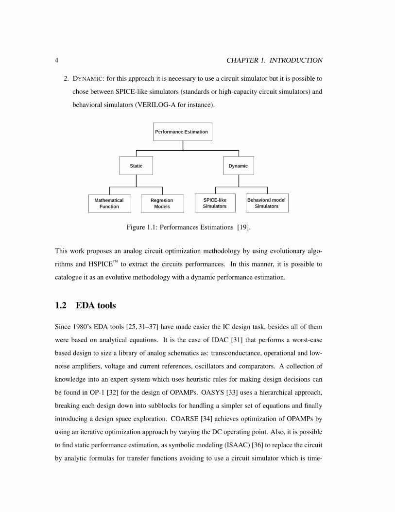
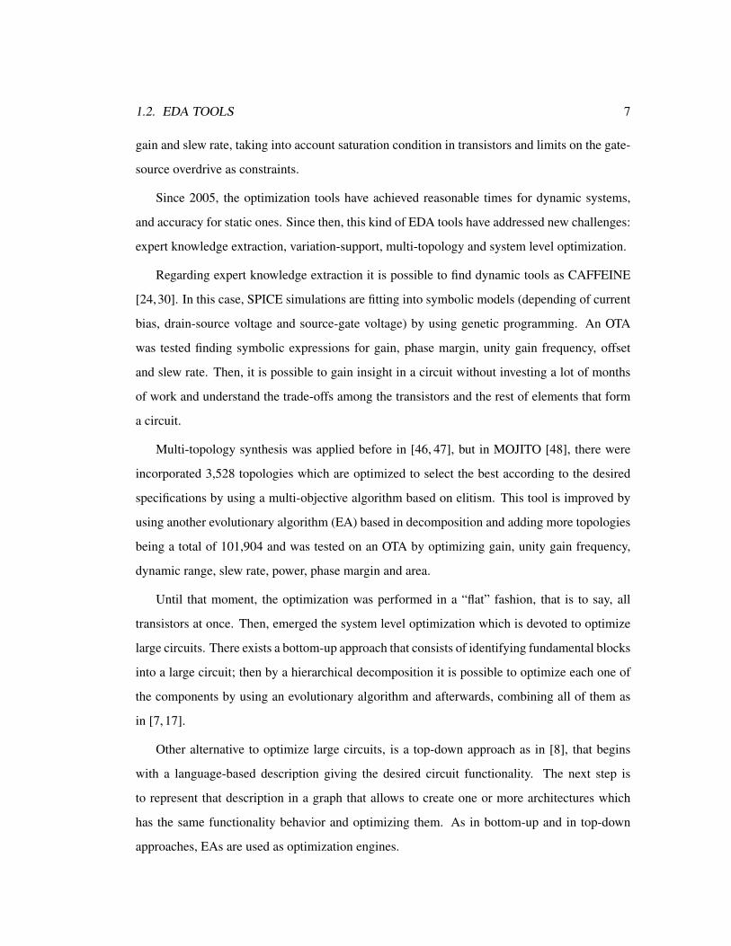
performance estimation possibilities with their own variants as depicted in Figure 1.1 [19,30] :
1. STATIC: in this case, the circuit or system will be replaced by a model (mathematical
equation or a regression model), which can be handled without the need to include a
circuit simulator, as a result it is possible to save time. To build the model it is possible to
make it by hand or automatically by using: symbolic analysis, neural networks, genetic
programming, among others. Finally, this implementation is always compared with a
circuit simulator to verify the solution really is correct.
4 CHAPTER 1. INTRODUCTION
2. DYNAMIC: for this approach it is necessary to use a circuit simulator but it is possible to
chose between SPICE-like simulators (standards or high-capacity circuit simulators) and
behavioral simulators (VERILOG-A for instance).
Performance Estimation
Dynamic Static
SPICE-like Simulators
Behavioral model Simulators
Mathematical Function
Regresion Models
Figure 1.1: Performances Estimations [19].
This work proposes an analog circuit optimization methodology by using evolutionary algo-
rithms and HSPICE™ to extract the circuits performances. In this manner, it is possible to
catalogue it as an evolutive methodology with a dynamic performance estimation.
1.2 EDA tools
Since 1980’s EDA tools [25, 31–37] have made easier the IC design task, besides all of them
were based on analytical equations. It is the case of IDAC [31] that performs a worst-case
based design to size a library of analog schematics as: transconductance, operational and low-
noise amplifiers, voltage and current references, oscillators and comparators. A collection of
knowledge into an expert system which uses heuristic rules for making design decisions can
be found in OP-1 [32] for the design of OPAMPs. OASYS [33] uses a hierarchical approach,
breaking each design down into subblocks for handling a simpler set of equations and finally
introducing a design space exploration. COARSE [34] achieves optimization of OPAMPs by
using an iterative optimization approach by varying the DC operating point. Also, it is possible
to find static performance estimation, as symbolic modeling (ISAAC) [36] to replace the circuit
by analytic formulas for transfer functions avoiding to use a circuit simulator which is time-

1.2. EDA TOOLS 5
consuming. However, the shortcoming was loss of accuracy.
Early’s 1990s, arose the “first generation” analog design optimization tools. Among the first
precursors is a static tool named OPTIMAN [38] that includes ISAAC for analytic modeling
of the circuits and the optimization is based on annealing. This tool was tested on a folded-
cascode OTA and on a switched-capacitor biquadratic filter, the optimized performances were:
unity gain frequency, power, gain, phase margin, slew rate, noise, output range, input range and
offset . SEAS [39] uses simulated evolution supported on design knowledge to optimize a two-
stage OPAMP and optimizing: unity gain frequency, gain , slew rate, CMRR, phase margin ,
power and output range. Until then, the knowledge was the common resource as circuit libraries
or design rules, while symbolic analysis was the other promising resource, but loss of accuracy
is needed to simplify the analytical models, otherwise would be impractical to optimize the long
terms.
During that decade, other tools that were proposed for local unconstrained optimizations
by a corner analysis trough a worst-case test as in SQP/EXCALIBUR [40], where a buffer
amplifier is optimized in unity gain frequency, gain, phase margin, slew rate and voltage swing.
However, that approach has two drawbacks, the first is an increase of the consumption time
and the second one is that for the recent technologies there are more corners which needs to be
simulated. Then, based on the worst-case idea, in [41] is used a concept called sensitivity band
by defining the bounds between performances and parameters of the circuit; the variation of the
parameters is made in terms of monotonicity, but due to its complexity, it is tested on linear
circuits.
An annealing constrained system was proposed with a static performance estimation
(ASTRX/OBLX) [42]. This time achieving to optimize a circuit in less time than before, due
to instead using SPICE-like simulator, it uses an asymptotic waveform evaluation. This sys-
tem was tested on a few OTA variants, among them: simple, cascode, folded cascode, and two
stage; always optimizing only up to two objectives and the rest specifications are included as
constraints. Effectively, this system optimizes in a reasonable time, preserving a reasonable pre-
diction error too; unfortunately, the time and complexity setup, increases as the design variables
increase.

6 CHAPTER 1. INTRODUCTION
Among the annealing dynamic approaches, there exists a multi-objective optimization of
analog circuits in [28], and it handles discrete values for the design values and proposes different
levels of constraints and a variation-aware technique based on the sensitivity of the objective
functions to include them into the optimization loop, showing the usefulness of these approaches
by optimizing two OPAMPs, a comparator and an analog buffer.
Another stochastic dynamic methodology named ANACONDA [27] was proposed by using
stochastic search mixed with evolutionary algorithms concepts; also a SPICE-like is included
simulator into the optimization loop and the system was tested on three OPAMPs. In this case
there are only two optimization objectives: area and power; but were taking as constraints: gain,
phase margin, noise, CMRR, PSRR, settling time and total harmonic distortion.
In [43] the simulated-based optimization is replaced with the use of transfer functions pre-
viously synthesized with a regression technique. An operational amplifier and a state variable
filter were tested with this method but the main disadvantages are that for each circuit it is nec-
essary to apply a properly regression technique and the global optimization algorithm can not
handle discontinuous transfer functions.
Continuing with regression techniques and support variation methodologies, in HOLMES
[44] are captured the relationships between design variables and performances. In this manner,
it includes statistical process variations by creating regression polynomial models and making a
statistical variation optimization from a distributed probability density functions; an OTA Miller
was tested with this method and the optimization performance was power-area with unity gain,
slew rate, gain and input-referred noise density as constraints.
Formal evolutionary systems began to appear in scene with the new century, for instance
WATSON [45], where are generated new sets of design variables using SPICE as simulator to
evaluate the performance of the given circuit and using a genetic multiobjective algorithm. The
performances (operating point, small-signal, noise and/or transient analysis ) are extracted from
the simulations and passed to a next optimization stage using accurate reduced-order models
to make a fit to a Pareto front. Two OTA are compared and optimized; the design variables
were widths and lengths of the transistors, the biasing current and compensation capacitance;
regarding to objectives, were optimized in: input-referred noise density, unity gain frequency,
1.2. EDA TOOLS 7
gain and slew rate, taking into account saturation condition in transistors and limits on the gate-
source overdrive as constraints.
Since 2005, the optimization tools have achieved reasonable times for dynamic systems,
and accuracy for static ones. Since then, this kind of EDA tools have addressed new challenges:
expert knowledge extraction, variation-support, multi-topology and system level optimization.
Regarding expert knowledge extraction it is possible to find dynamic tools as CAFFEINE
[24,30]. In this case, SPICE simulations are fitting into symbolic models (depending of current
bias, drain-source voltage and source-gate voltage) by using genetic programming. An OTA
was tested finding symbolic expressions for gain, phase margin, unity gain frequency, offset
and slew rate. Then, it is possible to gain insight in a circuit without investing a lot of months
of work and understand the trade-offs among the transistors and the rest of elements that form
a circuit.
Multi-topology synthesis was applied before in [46, 47], but in MOJITO [48], there were
incorporated 3,528 topologies which are optimized to select the best according to the desired
specifications by using a multi-objective algorithm based on elitism. This tool is improved by
using another evolutionary algorithm (EA) based in decomposition and adding more topologies
being a total of 101,904 and was tested on an OTA by optimizing gain, unity gain frequency,
dynamic range, slew rate, power, phase margin and area.
Until that moment, the optimization was performed in a “flat” fashion, that is to say, all
transistors at once. Then, emerged the system level optimization which is devoted to optimize
large circuits. There exists a bottom-up approach that consists of identifying fundamental blocks
into a large circuit; then by a hierarchical decomposition it is possible to optimize each one of
the components by using an evolutionary algorithm and afterwards, combining all of them as
in [7, 17].
Other alternative to optimize large circuits, is a top-down approach as in [8], that begins
with a language-based description giving the desired circuit functionality. The next step is
to represent that description in a graph that allows to create one or more architectures which
has the same functionality behavior and optimizing them. As in bottom-up and in top-down
approaches, EAs are used as optimization engines.
8 CHAPTER 1. INTRODUCTION
About variation-support optimization a natural way to include the variations in the opti-
mization process is by including a Monte Carlo analysis to each optimized solution as in [49],
unfortunately this is impractical because the consumption time increases considerably. A trust-
worthy analog EDA tool needs to offer robustness solutions enforcing the optimization tasks
with reasonable execution times, then the efforts have been focused to employ methods to avoid
expensive times without lost of accuracy [26, 50, 51].
Continuing with this trend, Kriging models [5], are used to address a statistical performance
for deterministic functions into stochastic process; two circuits were tested: LC oscillator and a
two-stage operational amplifier. Other example is Multi-yield Pareto fronts [6] that works with
the same methodology but applied to optimize a PLL.
Nevertheless, Monte Carlo based methodologies have been sumarized, for instance in [20,
52] that use Pareto surfaces, but this time, reducing the number of evaluations required in Monte
Carlo analysis ensuring accuracy by applying a Latin Hypercubes sampling.
1.3 Justification
Nowadays, hand-crafting analog design has to respond to the time-to-market constraints by
encouraging the industry to grow and improve analog EDA tools [3, 9]. Such tools, increase
productivity not only by reducing design time but also by diminishing the error-prone to which a
manual process is subject. Industrial circuit design requires not only optimized designs, but also
requires trustworthy and robustness to variations process. In this manner, the designer needs to
handle a large number of variables, often against each other, to consider all these issues and
performance requirements [4]. In this way, automated design of analog circuits has benefits for
industrial design process improving productivity mainly by reducing the design time as shown
in [3, 16, 30].
The academic efforts in this field have been fostered to the industry to use these method-
ologies. This is the case of Virtuoso NeoCircuit [53], Circuit Explorer [54], MunEDA [55],
Titan [56] and Arsyn [57], among others. In general, all of them include optimization tools,
which offers to accelerate the design process allowing designers to focus on creative tasks in-
stead of spending time in repetitive tasks. These tools are capable to optimize a circuit with
1.3. JUSTIFICATION 9
deterministic or stochastic methods taking into account constraints, some of them including
multi-objective optimization and including corner analysis.
Despite the different challenges in EDA tools, it is possible to find recent efforts to en-
hance the optimization task, especially by using EAs. Typically, EAs work with a set of
non-dominated solutions which are a powerful way to analyze data; because, unlike to sin-
gle solution methods, it is possible to identify and explore the trade-offs among the optimized
objectives. A great number of optimization EDA tools use an EA due to its high capability to
handle many variables and objectives taking into account constraints. Also, an EA is able to
find optimal Pareto fronts, at the same time, saving all the optimization process to reuse for post
analysis without having to resimulate. Some EAs, do not need much setup effort to scale the
number of variables,objectives and constraints. All these issues, are attractive features that have
been made that EAs achieve opportunities in analog circuit design optimization. From the state
of art, it is possible to see how EAs recently have leaded the analog design optimization tools,
then using them into optimization process, offers a promising field.
There are factors that have shown a marked viability on the development of automated
analog circuit design such as success of previous work on this field, constant improvement of
heuristics techniques and more computers capabilities such as speed and storage. In [4, 21, 44,
58] are agreements in the challenges and opportunities that each design problem presents. Also,
it is claimed that we are at the beginning of the evolution of the post-SPICE analog tools, and
is expected more improvements and accurate in circuit and level system.
The fraction of circuits that meets the specifications in a system among all the fabricated
circuits is called “yield” [20]. While a 0.35µm technology has a yield around 95%, a 90nm
technology has around 50% of yield for OTA’s, filters, integrators and comparators that exhibit
the similar performance levels [9, 58]. The relation between the performances and variation of
parameters of a circuit generally is non-linear but it is possible to simulate it [51]. Under these
conditions, a designer needs new tools to handle all the involved parameters in a circuit [9,
59] and for manufacture process, the optimization helps the designer to make high-performing
designs [6].
In this manner it is possible to identify the benefits of using optimization analog circuit

10 CHAPTER 1. INTRODUCTION
design tools, such as:
To validate if a design works properly, fulfilling the requirements, performances and trade-
offs.
To verify if a system architecture or selected topology is correct and meets specifications.
To experiment the circuit to know what are the design limits before failing, taking into
account more than one performance and/or constraint at the same time.
To explore what elements are more sensitive and if there are issues which have risk to design.
To make better decisions based on performance/contraints and the developed knowledge by
using these tools.
To enhance the circuit robustness by guaranteeing that the found solutions support process
variation.
To enhance circuits which have been previously hand crafted and have not reached their best
performances.
1.4 Objectives
The main goal is to propose an EDA methodology for analog circuit optimization by applying
EAs, encoding automatically the circuits and including support variation.
The proposed optimization will be based on HSPICE™ simulations and compiled on a open
source language code with the aim to be portable over the different operating systems.
It is possible to summarize the following objectives:
Getting highest-quality circuit performance tradeoffs.
Minimizing computational effort in the analog circuit optimization.
Maximizing robustness by including circuit variation-aware.
Exploring the behavior of the EAs with varying conditions of the genetic operators.
Calibrating and comparing some evolutionary algorithms.
Testing of the EAs with similar test functions including constraints.
Apply graph theory for the automatic biasing of the circuit under optimization.

1.4. OBJECTIVES 11
Analyze a variation-support strategy to enhance the solution feasibility.

12 CHAPTER 1. INTRODUCTION
1.5 Thesis Organization
This thesis is organized as follows. The second chapter is devoted to outline the basic concepts
about evolutionary algorithms, describes the multi-objective problem, the Pareto dominance and
the genetic operators used along this work. At the end of that chapter, there are exposed three
evolutionary algorithms to solving multi-objective problems by including constraints: Non-
Dominated Sorting Genetic Algorithm (NSGA-II), Multi-Objective Evolutionary Algorithm by
Decomposition (MOEAD) and Multi-Objective Particle Swarm Optimization (MOPSO) and a
brief comparison among them are made by optimizing mathematical functions with Simulated
Binary Cross-Over (SBX) and Differential Evolution (DE) as recombination operators.
The third chapter is devoted to show the circuit optimization methodology proposed in this
Thesis based on evolutionary algorithms. Next, is performed a comparison between SBX and
DE when are used in the optimization of eleven objectives of two mixed mode analog circuits:
a Positive-type Second Generation Current Conveyor (CCII+) encoded only with two variables
and a Negative-type Second Generation Current Conveyor (CCII−) encoded with eight vari-
ables. The chapter ends showing the optimization of nine amplifiers all of them with different
number of design variables and eleven objective functions.
A new current-branches-bias assignment approach is proposed in the fourth chapter with the
aim to accelerate the sizing process of analog integrated circuits composed of MOSFETs. This
methodology is used to initialize the evolutionary algorithms in the optimization of two am-
plifiers: a Folded Cascode (FC) Operational Transconductance Amplifier (OTA) encoded with
seven variables and a Recycled Folded Cascode (RFC) OTA encoded with ten variables. The
examples show a reduction of generations to find optimal solutions and increased the number of
biased solutions in less time comparing with the same optimization without using the proposed
methodology.
The fifth chapter outlines the yield and tolerance concepts for analog circuits. Next, there are
summarized the variation analysis approaches and there are grouping them in: worst case and
non-worst case approaches. Next, it is shown a Worst Case approach based on sensitivity and a
Non-WorstCase based on Monte Carlo simulation to broad the variation aware optimization of
analog circuits. A complete multi-objective optimization system is presented to perform these

1.5. THESIS ORGANIZATION 13
approaches, it is able to finding optimal solutions taking into account the fabrication process
variations.
The sixth chapter summarizes the conclusions around this work. Appendix A is devoted to
show the circuit optimizer software tool developed to perform all the circuit optimizations in
this work. In Appendix B are listed the transistor models to optimize all the circuits in Chapters
3 to 5.

14 CHAPTER 1. INTRODUCTION

Chapter 2
Evolutionary Algorithms
2.1 Introduction
This chapter consists of an outline about Evolutionary Algorithms (EA), first by defining the
main terms that are used continuously in this field, and second by describing the general proce-
dure of an EA. Next, are described three EAs and a brief comparison among them are made by
optimizing ZDT functions with SBX and DE as recombination operators.
2.2 Evolutionary Algorithms concepts
2.2.1 Individuals, Population, Evolutionary Operators and Objective Function
An individual represents an encoded solution to some specific problem. Each individual is
defined by a biological genotype, when the genotype is decoded (for instance to represent a spe-
cific circuit) then is named phenotype. A genotype is conformed by one or more chromosomes.
Such chromosomes in turn are composed of genes that have certain values named as alleles. A
locus is the position that an allele has within the chromosome. Figure 2.1 [60] depicts a chro-
mosome, that consists of n genes and each one has a specific value (allele) located in a specific
position (locus).
When an individual is represented by only one chromosome, the words: individual and
chromosome, are used to referring as the same; a set of individuals (or chromosomes) yield a
15
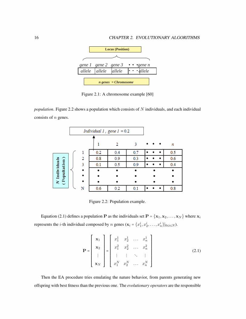
16 CHAPTER 2. EVOLUTIONARY ALGORITHMS
Locus (Position)
n genes = Chromosome
gene 1 gene 2 gene 3 gene n allele allele allele allele
Figure 2.1: A chromosome example [60]
population. Figure 2.2 shows a population which consists ofN individuals, and each individual
consists of n genes.
Figure 2.2: Population example.
Equation (2.1) defines a population P as the individuals set P = x1,x2, . . . ,xN where xi
represents the i-th individual composed by n genes (xi = xi1, xi2, . . . , xin∣0≤i≤N ).
P =
⎡⎢⎢⎢⎢⎢⎢⎢⎢⎢⎢⎢⎢⎣
x1
x2
⋮
xN
⎤⎥⎥⎥⎥⎥⎥⎥⎥⎥⎥⎥⎥⎦
=
⎡⎢⎢⎢⎢⎢⎢⎢⎢⎢⎢⎢⎢⎣
x11 x1
2 . . . x1n
x21 x2
2 . . . x2n
⋮ ⋮ ⋱ ⋮
xN1 xN2 . . . xNn
⎤⎥⎥⎥⎥⎥⎥⎥⎥⎥⎥⎥⎥⎦
(2.1)
Then the EA procedure tries emulating the nature behavior, from parents generating new
offspring with best fitness than the previous one. The evolutionary operators are the responsible

2.2. EVOLUTIONARY ALGORITHMS CONCEPTS 17
of this process, and such operators are three:
1. Mutation: consisting of selecting a parent to change the value of an allele choosing ran-
domly a locus.
2. Recombination: for instance, cross-over is a form of recombination and consists of se-
lecting parents (usually two) and each one is cut an recombined with the other part of the
other parent.
3. Selection: This process is the responsible to choose among all the parents and the off-
spring, such those that have the best fitness.
Then P is the set of individuals which conforms a population in the generation t, and ∣P∣
denotes the population size. It is possible to render the next population (Pt+1) from the cur-
rent population (Pt), by using evolutionary operators: µr denotes recombination, µm denotes
mutation and µs denotes selection evolutionary operators. The individuals in the current popu-
lation (Pt) are called “parents and the individuals in the next population (Pt+1) are called the
offspring.
An objective function is a feature of the problem domain and defines the EA’s optimality
condition. The fitness function allows to measure with a real-value a solution based in how
much satisfies the objective function(s).
2.2.2 The General Evolutionary Algorithm
The evolutionary task begins when an initialization procedure generates (usually randomly) a
population of individuals yielding the first parent population (Pt, the first generation is denoted
by t = 0) ; next, by using evolutionary operators (µr, µm and µs) a new population (Pt+1) is
generated yielding the offsprings (usually ∣Pt∣ = ∣Pt+1∣). Afterwards, a fitness function eval-
uation (from the objective functions) is performed for each new individual (xt+1) in the new
population (Pt+1), if the offsprings have better fitness than their parents, then the parents are
replaced by their offspring. Finally, a stop criterium (ξ) decides when the task should stop from
a set of parameters µξ. All this process is sumarized in the Algorithm 1 [61].
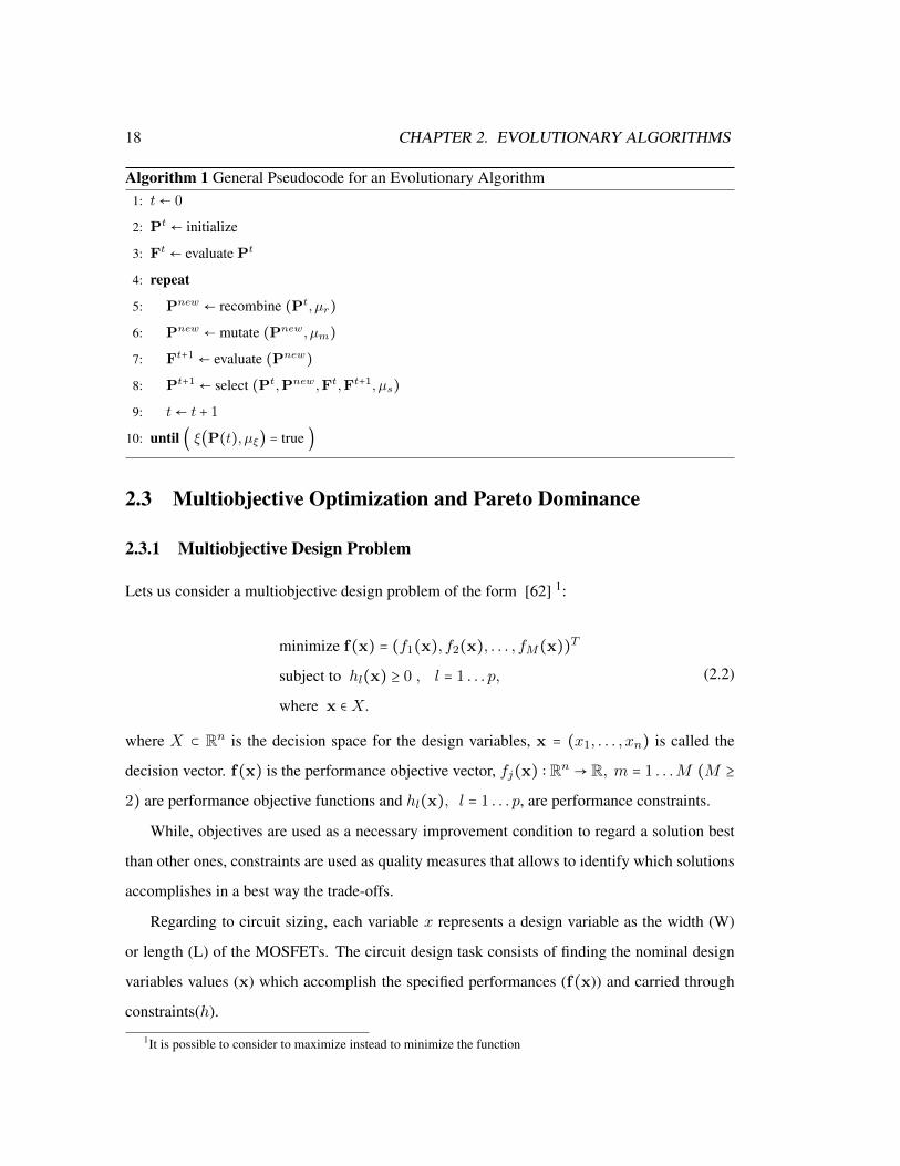
18 CHAPTER 2. EVOLUTIONARY ALGORITHMS
Algorithm 1 General Pseudocode for an Evolutionary Algorithm1: t← 0
2: Pt ← initialize
3: Ft ← evaluate Pt
4: repeat
5: Pnew ← recombine (Pt, µr)6: Pnew ← mutate (Pnew, µm)7: Ft+1 ← evaluate (Pnew)8: Pt+1 ← select (Pt,Pnew,Ft,Ft+1, µs)9: t← t + 1
10: until ( ξ(P(t), µξ) = true )
2.3 Multiobjective Optimization and Pareto Dominance
2.3.1 Multiobjective Design Problem
Lets us consider a multiobjective design problem of the form [62] 1:
minimize f(x) = (f1(x), f2(x), . . . , fM(x))T
subject to hl(x) ≥ 0 , l = 1 . . . p,
where x ∈X.
(2.2)
where X ⊂ Rn is the decision space for the design variables, x = (x1, . . . , xn) is called the
decision vector. f(x) is the performance objective vector, fj(x) ∶ Rn → R, m = 1 . . .M (M ≥
2) are performance objective functions and hl(x), l = 1 . . . p, are performance constraints.
While, objectives are used as a necessary improvement condition to regard a solution best
than other ones, constraints are used as quality measures that allows to identify which solutions
accomplishes in a best way the trade-offs.
Regarding to circuit sizing, each variable x represents a design variable as the width (W)
or length (L) of the MOSFETs. The circuit design task consists of finding the nominal design
variables values (x) which accomplish the specified performances (f(x)) and carried through
constraints(h).
1It is possible to consider to maximize instead to minimize the function
2.3. MULTIOBJECTIVE OPTIMIZATION AND PARETO DOMINANCE 19
2.3.2 Pareto Dominance
It is possible to define the Pareto dominance [63, 64] as xa ≺ xb (xa dominates xb) if all
fm(xa) in f(xa) are equal or better than all fm(xb) in f(xb) and at least one fm(xa) is better
than fm(xb) (for m = 1, . . . ,M ), where better means less when the objective is to minimize
and high when the objective is to maximize.
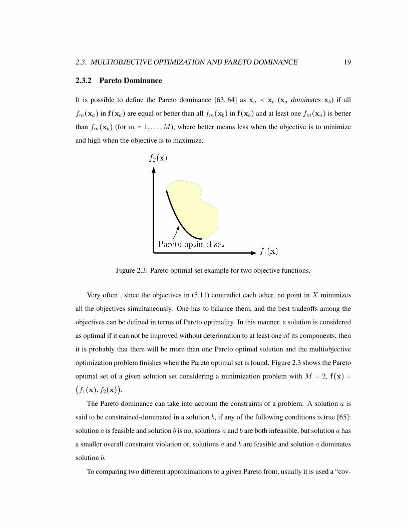
Figure 2.3: Pareto optimal set example for two objective functions.
Very often , since the objectives in (5.11) contradict each other, no point in X minimizes
all the objectives simultaneously. One has to balance them, and the best tradeoffs among the
objectives can be defined in terms of Pareto optimality. In this manner, a solution is considered
as optimal if it can not be improved without deterioration to at least one of its components; then
it is probably that there will be more than one Pareto optimal solution and the multiobjective
optimization problem finishes when the Pareto optimal set is found. Figure 2.3 shows the Pareto
optimal set of a given solution set considering a minimization problem with M = 2, f(x) =
(f1(x), f2(x)).
The Pareto dominance can take into account the constraints of a problem. A solution a is
said to be constrained-dominated in a solution b, if any of the following conditions is true [65]:
solution a is feasible and solution b is no, solutions a and b are both infeasible, but solution a has
a smaller overall constraint violation or, solutions a and b are feasible and solution a dominates
solution b.
To comparing two different approximations to a given Pareto front, usually it is used a “cov-
20 CHAPTER 2. EVOLUTIONARY ALGORITHMS
erage metric” [66]. Let A and B be two approximations to the Pareto front of a multi-objective
problem. C(A,B) is defined as the percentage of the solutions in B that are dominated by at
least one solution in A [65]:
C(A,B) = ∣ u ∈ B ∣ ∃v ∈ A ∶ v dominates u ∣∣ B ∣ (2.3)
C(A,B) is not necessarily equal to 1-C(B,A). C(A,B) = 1 means that all solutions in B
are dominated by some solutions in A.
2.3.3 Diversity and Efficiency
When we have a problem to solve, there may be several suitable algorithms available. We would
obviously like to choose the best, in such a manner, it raises the question of how to decide which
is preferable. Besides the solution convergence when the optimization experiment is repeated,
there exists two features that allow to compare among algorithms.
An important EA feature is diversity [60], which consists of avoiding that the entire popula-
tion converges to a single point ignoring the rest of the search space. It is desirable to preserve
diversity and the convergence of the solutions to the Pareto front at the same time, when a
experiment is repeated trough different runs.
Also, it is possible to define the efficiency of an algorithm as simply how fast it runs, then it
is necessary to express the unit for the theoretical efficiency of an algorithm, as the time taken by
an algorithm within a multiplicative constant. This concept works regardless the programming
language, the compiler used, the skill of the programmer and the implementation hardware [67].
We usually do not know the problem size beforehand, and either, if all problems require
the entire range of functions in the algorithm. Then, it is considered an asymptotic behavior
of the algorithm for a very large problem size, this behavior is expressed in an Asymptotic
Notation [68]. Among the most important asymptotic notations is the “Big Oh”2 notation that
is a mathematical symbol to denote: “the order of ”.
2There exists other notations as omega, theta and little oh.
2.4. GENETIC OPERATORS 21
2.4 Genetic Operators
The genetic operators are used in EAs in order to recombine existing individuals (or solutions)
of the current generation to render a new one individual. A genetic operator helps along the op-
timization procedure, to converge to the Pareto front and to preserve diversity, then the success
of the optimization largely depends on these operators.
The basic genetic operators are crossover and mutation [69] but exist other operators as
Simulated Binary Cross-Over Operator (SBX) [70] and Differential Evolution (DE) [71] which
have shown to improve the performance of basic operators.
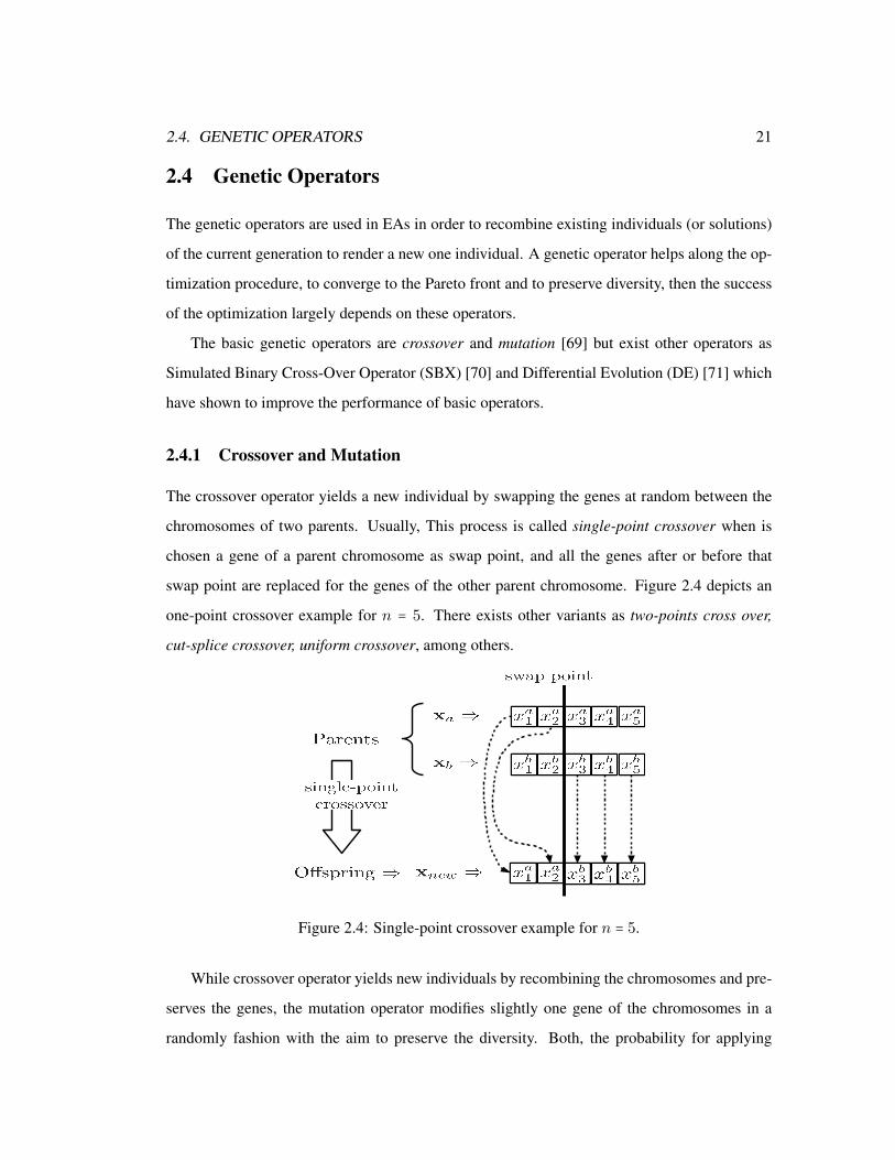
2.4.1 Crossover and Mutation
The crossover operator yields a new individual by swapping the genes at random between the
chromosomes of two parents. Usually, This process is called single-point crossover when is
chosen a gene of a parent chromosome as swap point, and all the genes after or before that
swap point are replaced for the genes of the other parent chromosome. Figure 2.4 depicts an
one-point crossover example for n = 5. There exists other variants as two-points cross over,
cut-splice crossover, uniform crossover, among others.
Figure 2.4: Single-point crossover example for n = 5.
While crossover operator yields new individuals by recombining the chromosomes and pre-
serves the genes, the mutation operator modifies slightly one gene of the chromosomes in a
randomly fashion with the aim to preserve the diversity. Both, the probability for applying
22 CHAPTER 2. EVOLUTIONARY ALGORITHMS
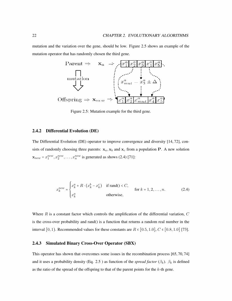
mutation and the variation over the gene, should be low. Figure 2.5 shows an example of the
mutation operator that has randomly chosen the third gene.
Figure 2.5: Mutation example for the third gene.
2.4.2 Differential Evolution (DE)
The Differential Evolution (DE) operator to improve convergence and diversity [14, 72], con-
sists of randomly choosing three parents: xa,xb and xc from a population P. A new solution
xnew = xnew1 , xnew2 , . . . , xnewn is generated as shows (2.4) [71]:
xnewk =⎧⎪⎪⎪⎪⎨⎪⎪⎪⎪⎩
xak +R ⋅ (xbk − xck) if rand() < C,
xak otherwise,for k = 1,2, . . . , n. (2.4)
Where R is a constant factor which controls the amplification of the differential variation, C
is the cross-over probability and rand() is a function that returns a random real number in the
interval [0,1). Recommended values for these constants are R ∈ [0.5,1.0], C ∈ [0.8,1.0] [73].
2.4.3 Simulated Binary Cross-Over Operator (SBX)
This operator has shown that overcomes some issues in the recombination process [65, 70, 74]
and it uses a probability density (Eq. 2.5 ) as function of the spread factor (βk). βk is defined
as the ratio of the spread of the offspring to that of the parent points for the k-th gene.
2.4. GENETIC OPERATORS 23
P (βk) =⎧⎪⎪⎪⎪⎨⎪⎪⎪⎪⎩
0.5(η + 1)βηk if βηk ≤ 1
0.5(η + 1) 1
βη+2k
otherwise(2.5)
The η is an integer value called distribution index. This operator allows creating two off-
springs at the same time as shows (2.6) [65], where xa and xb are the parents and xnew1 and
xnew2 are the offspring.
xnew1k = 0.5[(1 + βq) ⋅ xak + (1 − βq) ⋅ xbk]
xnew2k = 0.5[(1 − βq) ⋅ xak + (1 + βq) ⋅ xbk]
(2.6)
βq is defined as (2.7) where ρ is a random real number in the interval [0,1).
ρ = rand()
βq =⎧⎪⎪⎪⎨⎪⎪⎪⎩
(2ρ)1
ηc+1 if ρ ≤ 0.5
( 12(1−ρ))
1ηc+1 otherwise
(2.7)
2.4.4 Polynomial Mutation
Polynomial mutation [65, 75] as SBX, uses a specific probability density shown in (2.8) where
ρ is a random real number in the interval [0,1) and ηm is an integer number.
δk =⎧⎪⎪⎪⎨⎪⎪⎪⎩
(2ρ)1
ηm+1 − 1 if ρ < 0.5
1 − [(2ρ)1
ηm+1 ] otherwise(2.8)
The mutation can be performed as (2.9), where xLk and xUk are the lower and upper bounds
values for the k-th gene, respectively, and xnew is a given individual in the next generation.
xnewk = xnewk + (xUk − xLk ) ⋅ δk (2.9)

24 CHAPTER 2. EVOLUTIONARY ALGORITHMS
2.5 NSGA-II, MOEAD and MOPSO
2.5.1 Non-Dominated Sorting Genetic Algorithm II (NSGA-II)
This is an improved version of a previous NSGA algorithm by including elitism and was named
as NSGA-II. Algorithm 2 [76, 77] summarizes the NSGA-II procedure and its efficiency is
O(mN2), where m is the number of objectives and N is the population size. NSGA-II approx-
imates the Pareto Front of a MOP by sorting and ranking all solutions in order to choose the
better solutions to make a new offspring, this means, by ranking all the population in different
Pareto subfronts that it will be possible to know which solutions show better performance.
Algorithm 2 NSGA-II Algorithm1: P0=random, Q0=random
2: t=0
3: Pt+1 = ∅ and i = 1
4: repeat
5: Rt = Pt ∪Qt6: F= fast-non-dominated-sort(Rt)
7: crowding-distance-assignment(Fi)
8: repeat
9: Pt+1 = Pt+1 ∪ Fi10: i = i + 1
11: until ∣Pt+1∣ + ∣Fi∣ ≤ N12: Sort(Fi,≺n)
13: Pt+1 = Pt+1 ∪ Fi[1 ∶ (N − ∣Pt+1∣)]14: Qt+1=make-new-pop(Pt+1)
15: until stop criteria
In this algorithm is contemplated a way to choose the best solution between two solutions
in the same subfront preserving diversity, in this form it is possible to select the best part of a
population without losing diversity.
Then NSGA-II is based on two main procedures : Fast Nondominated Sort and Crowding
Distance Assignment. These two procedures ensure elitism and it is possible to add constraints
2.5. NSGA-II, MOEAD AND MOPSO 25
to ensure that the solutions are feasible [76].
At the beginning, it is necessary to randomly initialize the parameters and start by generating
two populations (Po and Qo) each one of size N , from random values into a feasible region.
The NSGA-II procedure in each generation consists of rebuilding the current population (Rt)
from the two original populations (Pt and Qt) then the new size of current population will be
2N .
Now through a nondominated sorting all solutions in Rt are ranked, and classified in a
family of subfronts. In the next step is necessary to create from the current population Rt
(previously ranked and ordered by subfront number) a new offspring (Pt+1), the objective will
be to choose from a population of size 2N , the N solutions which belong to the first subfronts.
In this manner, the last subfront could be greater than necessary, then a measure (idistance) is
used to identify the better solutions and preserving elitism by selecting the solutions that are
far the rest, this is possible simply by modifying a little bit the concept of Pareto dominance as
follows:
i ≺n j if [(irank < jrank) or (irank = jrank)] and (idistance > jdistance)
Fast Non-Dominated Sort: Algorithm 3 shows this procedure which is responsible to rank
each solution into a subfront, and starts by selecting the nondominated solutions among the
current population (Rt). This first group of solutions will be labeled as the solutions into the
first subfront (F1) and are separated from Rt. For the remaining solutions in Rt are selected the
nondominated solutions again but this time they are labeled into the second subfront (F2) and
separated from Rt like the solutions in (F1) were separated before. This procedure continues
until all solutions in Rt are ranked into a subfront.
The procedure uses a counter for each solution, such counter allows us to know how many
solutions dominate to each solution (np where p is the p-solution). In the same way, there
is a set which contains all the solutions dominated for each solution (all solutions in Sp are
dominated by p-solution ). First are taken the solutions with counter equal to zero and to each
solution in their set of dominated solutions are diminished their counters in one. In this way
the next subfront is composed by the remaining solutions with counter equal to zero. This
continues until all solutions have been ranked. In Figure 2.6 there is an outcome example of
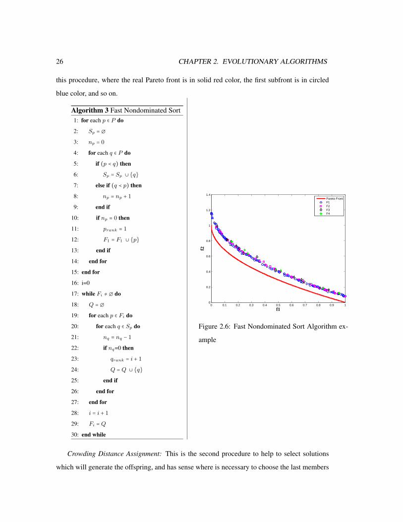
26 CHAPTER 2. EVOLUTIONARY ALGORITHMS
this procedure, where the real Pareto front is in solid red color, the first subfront is in circled
blue color, and so on.
Algorithm 3 Fast Nondominated Sort1: for each p ∈ P do
2: Sp = ∅3: np = 0
4: for each q ∈ P do
5: if (p ≺ q) then
6: Sp = Sp ∪ q7: else if (q ≺ p) then
8: np = np + 1
9: end if
10: if np = 0 then
11: prank = 1
12: F1 = F1 ∪ p13: end if
14: end for
15: end for
16: i=0
17: while Fi ≠ ∅ do
18: Q = ∅19: for each p ∈ Fi do
20: for each q ∈ Sp do
21: nq = nq − 1
22: if nq=0 then
23: qrank = i + 1
24: Q = Q ∪ q25: end if
26: end for
27: end for
28: i = i + 1
29: Fi = Q30: end while
0 0.1 0.2 0.3 0.4 0.5 0.6 0.7 0.8 0.9 10
0.2
0.4
0.6
0.8
1
1.2
1.4
f1
f2
Pareto FrontF1F2F3F4
Figure 2.6: Fast Nondominated Sort Algorithm ex-
ample
Crowding Distance Assignment: This is the second procedure to help to select solutions
which will generate the offspring, and has sense where is necessary to choose the last members

2.5. NSGA-II, MOEAD AND MOPSO 27
Algorithm 4 Crowding Distance Assignment
1: l = ∣T ∣2: for each i do
3: set T [i]distance = 0
4: for each objective m do
5: T= sort(T,m)
6: T [1]distance = T [l]distance =∞7: for i = 2 to (l-1) do
8: T [i]distance = T [i]distance + (T [i + 1] ⋅m − T [i − 1] ⋅m)/(fmaxm − fminm )9: end for
10: end for
11: end for
of the population Pt+1 into a subfront, because all subfront members then have other ranking
parameters into their subfront. The main idea is to perform a density estimation named crowding
distance (idistance) by sorting in ascending order the solutions for each objective function, then
for each objective it is first selected the smallest and largest limit found and an infinite value is
assigned to their crowding distances. Algorithm 4 shows the pseudocode for this procedure.
2.5.2 Multi-Objective Evolutionary Algorithm based on Decomposition (MOEAD)
The basic idea of MOEAD is the decomposition of a multiobjective problem in scalar optimiza-
tion subproblems by a weights vector. This vector associates a weight (λ) for each subproblem
which is considered as a single individual in the population which is going to try to improve by
itself and to its nearby (neighbors) .
After the initialization of the parameters the first step in MOEAD is related to define the N
spread weights vector over the objectives space (to each individual corresponds one λi). One
way can be by using a parameter H in a sequence as described by (2.10):
0
H,
1
H, . . . ,
H
H (2.10)
In Algorithms 5 and 6 are depicted the pseudocode to generate these vectors, for three and m
objectives respectively. It is necessary to chose a value for H and depending on this number the
28 CHAPTER 2. EVOLUTIONARY ALGORITHMS
population size is set.
Algorithm 5 Build spread of N
weight vectors (M = 3)1: i = 1, set H
2: for µ1 = 0 to 1, step 1H
do
3: for µ2 = 0 to 1, step 1H
do
4: if 1 − (µ1 + µ2) ≥ 0 then
5: λi = µ1 µ2 . . . (1 − (µ1 + µ2))6: i = i + 1
7: end if
8: end for
9: end for
Algorithm 6 Build spread of N weight vectors for
M objectives1: i = 1, set H
2: for µ1 = 0 to 1, step 1H
do
3: for µ2 = 0 to 1, step 1H
do
4: ⋱5: for µM−1 = 0 to 1, step 1
Hdo
6: if 1 − (µ1 + µ2 + . . . µM−1) ≥ 0 then
7: λi = µ1 µ2 . . . (1 − (µ1 + µ2 + . . . µM−1))8: i = i + 1
9: end if
10: end for
11: ⋰12: end for
13: end for
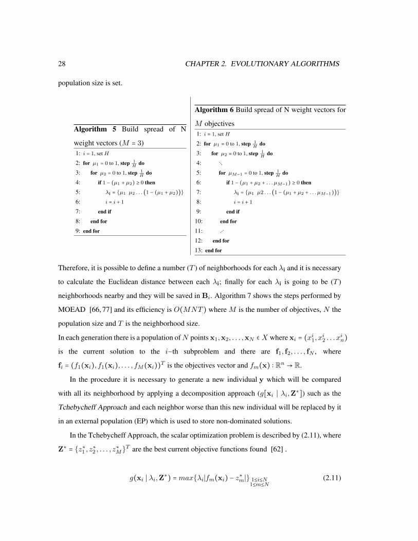
Therefore, it is possible to define a number (T ) of neighborhoods for each λi and it is necessary
to calculate the Euclidean distance between each λi; finally for each λi is going to be (T )
neighborhoods nearby and they will be saved in Bi. Algorithm 7 shows the steps performed by
MOEAD [66, 77] and its efficiency is O(MNT ) where M is the number of objectives, N the
population size and T is the neighborhood size.
In each generation there is a population ofN points x1,x2, . . . ,xN ∈X where xi = (xi1, xi2 . . . xin)
is the current solution to the i−th subproblem and there are f1, f2, . . . , fN , where
fi = (f1(xi), f1(xi), . . . , fM(xi))T is the objectives vector and fm(x) ∶ Rn → R.
In the procedure it is necessary to generate a new individual y which will be compared
with all its neighborhood by applying a decomposition approach (g[xi ∣ λi,Z∗]) such as the
Tchebycheff Approach and each neighbor worse than this new individual will be replaced by it
in an external population (EP) which is used to store non-dominated solutions.
In the Tchebycheff Approach, the scalar optimization problem is described by (2.11), where
Z∗ = z∗1 , z∗2 , . . . , z∗MT are the best current objective functions found [62] .
g(xi ∣ λi,Z∗) =maxλi∣fm(xi) − z∗m∣ 1≤i≤N1≤m≤N
(2.11)

2.5. NSGA-II, MOEAD AND MOPSO 29
Algorithm 7 MOEAD Algorithm1: build an uniform spread of N weight vectors (λ)
2: for i = 1,2, . . . ,N do
3: Bi = bi1, bi2, . . . , biT 4: end for
5: t = 1 , POP=random() , set E = ∅ , T
6: repeat
7: for i = 1,2, . . . ,N do
8: randomly select parents from Bi
9: generate new individual y
10: for each ` ∈ Bi do
11: if g(y ∣ λ`,Z∗) ≤ g(x` ∣ λ`,Z∗) then
12: x` = y
13: f` = f(y)14: end if
15: end for
16: end for
17: remove from EP all vectors dominated by f(y)18: until stop criteria
2.5.3 Multi-Objective Particle Swarm Optimization (MOPSO)
In the Multi-Objective Particle Swarm Optimization Algorithm (MOPSO) there are N particles
denoted by xi where i = 1,2, . . . ,N , and are represented by their positions in the search space.
Each particle xi = (xi1, xi2 . . . xin) represents a position in the space and depends of its previous
local best value (xbesti), and the previous global best value (xbestg). To compute the speed of
each particle the expression in (2.12) [78] is used.
V ik = kwV i
k +R1(x(best,i)k − xik) +R2(xbestgk − xik)∣1≤i≤N1≤k≤n
(2.12)
Vi is the current velocity of the particle i-th, kw is the inertia weight which takes typical values
less than 1; x(best,i) is the best position of particle i-th , xi is the position of the current particle
and xbestg is a global best selected among the global best solutions. R1 and R2 are random

30 CHAPTER 2. EVOLUTIONARY ALGORITHMS
real numbers in the interval (−1,1). The new position of each particle is computed as Equation
(2.13).
xik = xik + V ik (2.13)
Algorithm 8 Pseudocode for MOPSO1: Initialize NoLoops, bound limits, population (N ) and velocities
2: Evaluate population
3: for i=1 to N do
4: x(best,i) ← xi
5: end for
6: Select non-dominated particles and save them in REP
7: for t= 1 to NoLoops do
8: for i=1 to N do
9: xbestg ← Select randomly among solutions in REP
10: Update particle velocity
11: Update particle position
12: Ensuring new position is into bound limits
13: end for
14: Evaluate population
15: for i = 1 to N do
16: Update x(best,i)
17: end for
18: Select non-dominated particles and save them in REP
19: end for
Algorithm 8 shows the pseudo-code for MOPSO [79] and its efficiency is O(mN), where
m is the number of objectives and N is the population size.
In line 1 there is the initialization procedure where the bound limits are set, and the parti-
cles are initialized randomly inside these bound limits. The velocities are initialized with zero
values. In line 2, the population is evaluated to update the best position (xbest,i) at line 3, for
each particle. Afterwards in line 6, the non-dominated particles are gathered into a repository
(REP ). The optimization procedure begins in line 7, and for each particle is selected a best
2.5. NSGA-II, MOEAD AND MOPSO 31
particle among the solutions in REP (line 9). Then the velocity and position of each particle
is updated by using Equations (2.12) and (2.13), and avoiding going beyond the bound limits
(lines 10 to 12). Once all the particles are updated, then an evaluation process is applied to up-
date the best position for each particle and finally the non-dominated particles are selected and
saved in a repository (REP)(lines 14 to 18) .This process continues until a determined number
of loops or until a stop criterium.
2.5.4 Behavior of NSGA-II, MOEAD and MOPSO on test functions ZDT
Zitzler et al. [80], provided a comparison of various evolutionary approaches to multiobjective
optimization using six carefully chosen test functions, each one involves a particular feature,
that is known to cause difficulty in the evolutionary optimization process, mainly in converging
to the Pareto-optimal front. In Table 2.1, the four test functions used in this work are shown,
where ZDT1, ZDT2, ZDT3 and ZDT4 are the name of the selected functions, n is the
number of variables used for the functions, and bounds are the maximum and minimum search
limits for each variable. For the four selected functions the goal is to minimize the functions
given. The test function ZDT1 has a convex Pareto-optimal front, ZDT2 is the nonconvex
contrapart to ZDT1. ZDT3 represents the discreteness feature, its Pareto-optimal front consist
of several noncontiguous convex parts. ZDT4 contains 219 local Pareto-optimal fronts then it
tests the EA’s ability to deal with multimodality.
There were performed different experiments with the ZDT functions for NSGA-II, MOEAD
and MOPSO by using two different evolutionary operators: DE and SBX. The aim is to show
the usefulness of those three different evolutionary algorithms and their performance by using
different evolutionary operators along ten runs to make an statistical study of the dominance of
each one of the experiments compared with the others. All the runs were performed with a pop-
ulation size of 300 individuals for the ZDT functions listed on Table 2.1 over 1000 generations
and along ten runs. The results for all these experiments are showed in Figs. 2.7-2.11 where the
solid line depicts the goal for each ZDT function.
Finally in Table 2.2 are listed the statistical results for all these experiments with 5 variables,
by calculating the coverage metric of each method (rows) on the other methods (columns). In
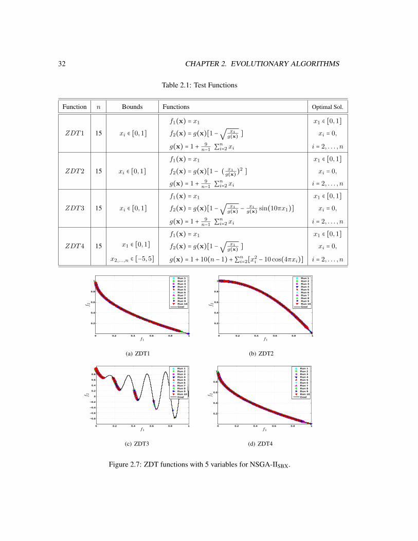
32 CHAPTER 2. EVOLUTIONARY ALGORITHMS
Table 2.1: Test Functions
Function n Bounds Functions Optimal Sol.
ZDT1 15 xi ∈ [0,1]f1(x) = x1 x1 ∈ [0,1]f2(x) = g(x)[1 −
√x1
g(x)] xi = 0,
g(x) = 1 + 9n−1 ∑
ni=2 xi i = 2, . . . , n
ZDT2 15 xi ∈ [0,1]f1(x) = x1 x1 ∈ [0,1]f2(x) = g(x)[1 − ( x1
g(x))2 ] xi = 0,
g(x) = 1 + 9n−1 ∑
ni=2 xi i = 2, . . . , n
ZDT3 15 xi ∈ [0,1]f1(x) = x1 x1 ∈ [0,1]f2(x) = g(x)[1 −
√x1
g(x)− x1
g(x)sin(10πx1)] xi = 0,
g(x) = 1 + 9n−1 ∑
ni=2 xi i = 2, . . . , n
ZDT4 15 x1 ∈ [0,1]
x2,...,n ∈ [−5,5]
f1(x) = x1 x1 ∈ [0,1]f2(x) = g(x)[1 −
√x1
g(x)] xi = 0,
g(x) = 1 + 10(n − 1) +∑ni=2[x2i − 10 cos(4πxi)] i = 2, . . . , n
0 0.2 0.4 0.6 0.8 1
0.2
0.4
0.6
0.8
1
f1
f 2
Run 1Run 2Run 3Run 4Run 5Run 6Run 7Run 8Run 9Run 10Goal
(a) ZDT1
0 0.2 0.4 0.6 0.8 1
0.2
0.4
0.6
0.8
1
f1
f 2
Run 1Run 2Run 3Run 4Run 5Run 6Run 7Run 8Run 9Run 10Goal
(b) ZDT2
0 0.2 0.4 0.6 0.8 1
−0.8
−0.6
−0.4
−0.2
0
0.2
0.4
0.6
0.8
1
f1
f 2
Run 1Run 2Run 3Run 4Run 5Run 6Run 7Run 8Run 9Run 10Goal
(c) ZDT3
0 0.2 0.4 0.6 0.8 1
0.2
0.4
0.6
0.8
1
f1
f 2
Run 1Run 2Run 3Run 4Run 5Run 6Run 7Run 8Run 9Run 10Goal
(d) ZDT4
Figure 2.7: ZDT functions with 5 variables for NSGA-IISBX.
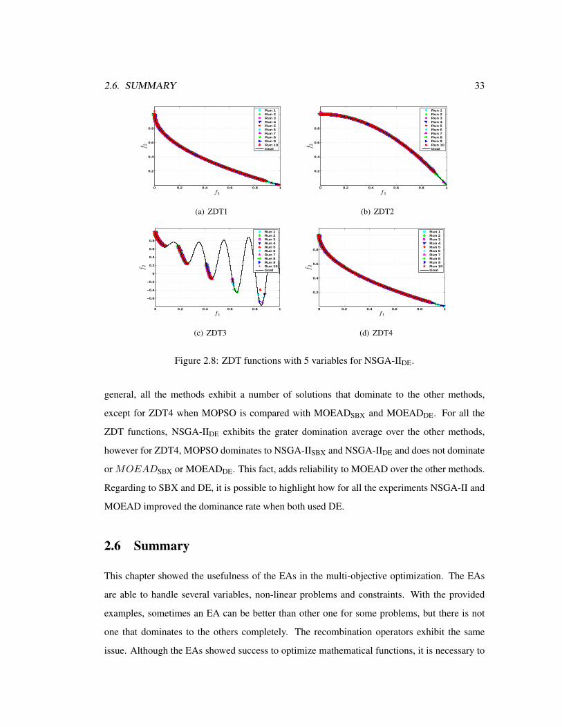
2.6. SUMMARY 33
0 0.2 0.4 0.6 0.8 1
0.2
0.4
0.6
0.8
1
f1
f 2
Run 1Run 2Run 3Run 4Run 5Run 6Run 7Run 8Run 9Run 10Goal
(a) ZDT1
0 0.2 0.4 0.6 0.8 1
0.2
0.4
0.6
0.8
1
f1
f 2
Run 1Run 2Run 3Run 4Run 5Run 6Run 7Run 8Run 9Run 10Goal
(b) ZDT2
0 0.2 0.4 0.6 0.8 1
−0.6
−0.4
−0.2
0
0.2
0.4
0.6
0.8
1
f1
f 2
Run 1Run 2Run 3Run 4Run 5Run 6Run 7Run 8Run 9Run 10Goal
(c) ZDT3
0 0.2 0.4 0.6 0.8 1
0.2
0.4
0.6
0.8
1
f1f 2
Run 1Run 2Run 3Run 4Run 5Run 6Run 7Run 8Run 9Run 10Goal
(d) ZDT4
Figure 2.8: ZDT functions with 5 variables for NSGA-IIDE.
general, all the methods exhibit a number of solutions that dominate to the other methods,
except for ZDT4 when MOPSO is compared with MOEADSBX and MOEADDE. For all the
ZDT functions, NSGA-IIDE exhibits the grater domination average over the other methods,
however for ZDT4, MOPSO dominates to NSGA-IISBX and NSGA-IIDE and does not dominate
or MOEADSBX or MOEADDE. This fact, adds reliability to MOEAD over the other methods.
Regarding to SBX and DE, it is possible to highlight how for all the experiments NSGA-II and
MOEAD improved the dominance rate when both used DE.
2.6 Summary
This chapter showed the usefulness of the EAs in the multi-objective optimization. The EAs
are able to handle several variables, non-linear problems and constraints. With the provided
examples, sometimes an EA can be better than other one for some problems, but there is not
one that dominates to the others completely. The recombination operators exhibit the same
issue. Although the EAs showed success to optimize mathematical functions, it is necessary to
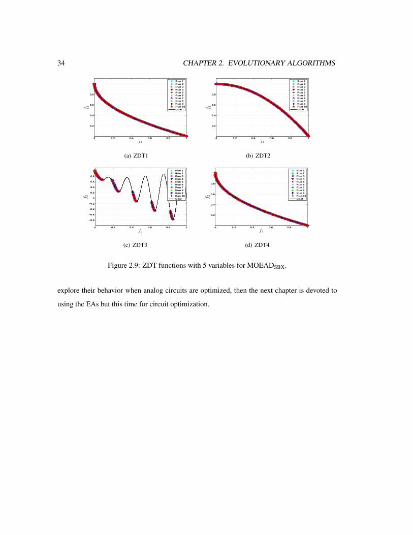
34 CHAPTER 2. EVOLUTIONARY ALGORITHMS
0 0.2 0.4 0.6 0.8 1
0.2
0.4
0.6
0.8
1
f1
f 2
Run 1Run 2Run 3Run 4Run 5Run 6Run 7Run 8Run 9Run 10Goal
(a) ZDT1
0 0.2 0.4 0.6 0.8 1
0.2
0.4
0.6
0.8
1
f1
f 2
Run 1Run 2Run 3Run 4Run 5Run 6Run 7Run 8Run 9Run 10Goal
(b) ZDT2
0 0.2 0.4 0.6 0.8 1
−0.8
−0.6
−0.4
−0.2
0
0.2
0.4
0.6
0.8
1
f1
f 2
Run 1Run 2Run 3Run 4Run 5Run 6Run 7Run 8Run 9Run 10Goal
(c) ZDT3
0 0.2 0.4 0.6 0.8 1
0.2
0.4
0.6
0.8
1
f1
f 2
Run 1Run 2Run 3Run 4Run 5Run 6Run 7Run 8Run 9Run 10Goal
(d) ZDT4
Figure 2.9: ZDT functions with 5 variables for MOEADSBX.
explore their behavior when analog circuits are optimized, then the next chapter is devoted to
using the EAs but this time for circuit optimization.
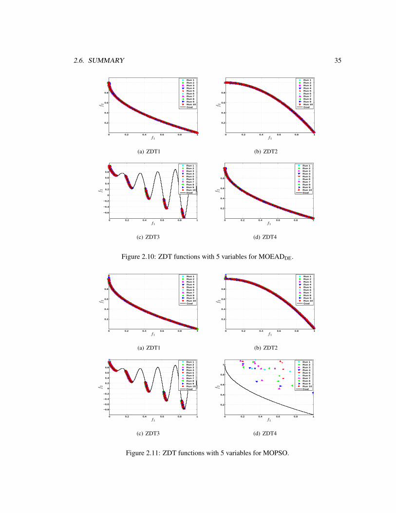
2.6. SUMMARY 35
0 0.2 0.4 0.6 0.8 1
0.2
0.4
0.6
0.8
1
f1
f 2
Run 1Run 2Run 3Run 4Run 5Run 6Run 7Run 8Run 9Run 10Goal
(a) ZDT1
0 0.2 0.4 0.6 0.8 1
0.2
0.4
0.6
0.8
1
f1
f 2
Run 1Run 2Run 3Run 4Run 5Run 6Run 7Run 8Run 9Run 10Goal
(b) ZDT2
0 0.2 0.4 0.6 0.8 1
−0.6
−0.4
−0.2
0
0.2
0.4
0.6
0.8
1
f1
f 2
Run 1Run 2Run 3Run 4Run 5Run 6Run 7Run 8Run 9Run 10Goal
(c) ZDT3
0 0.2 0.4 0.6 0.8 1
0.2
0.4
0.6
0.8
1
f1
f 2
Run 1Run 2Run 3Run 4Run 5Run 6Run 7Run 8Run 9Run 10Goal
(d) ZDT4
Figure 2.10: ZDT functions with 5 variables for MOEADDE.
0 0.2 0.4 0.6 0.8 1
0.2
0.4
0.6
0.8
1
f1
f 2
Run 1Run 2Run 3Run 4Run 5Run 6Run 7Run 8Run 9Run 10Goal
(a) ZDT1
0 0.2 0.4 0.6 0.8 1
0.2
0.4
0.6
0.8
1
f1
f 2
Run 1Run 2Run 3Run 4Run 5Run 6Run 7Run 8Run 9Run 10Goal
(b) ZDT2
0 0.2 0.4 0.6 0.8 1
−0.8
−0.6
−0.4
−0.2
0
0.2
0.4
0.6
0.8
1
f1
f 2
Run 1Run 2Run 3Run 4Run 5Run 6Run 7Run 8Run 9Run 10Goal
(c) ZDT3
0 0.2 0.4 0.6 0.8 1
0.2
0.4
0.6
0.8
1
f1
f 2
Run 1Run 2Run 3Run 4Run 5Run 6Run 7Run 8Run 9Run 10Goal
(d) ZDT4
Figure 2.11: ZDT functions with 5 variables for MOPSO.
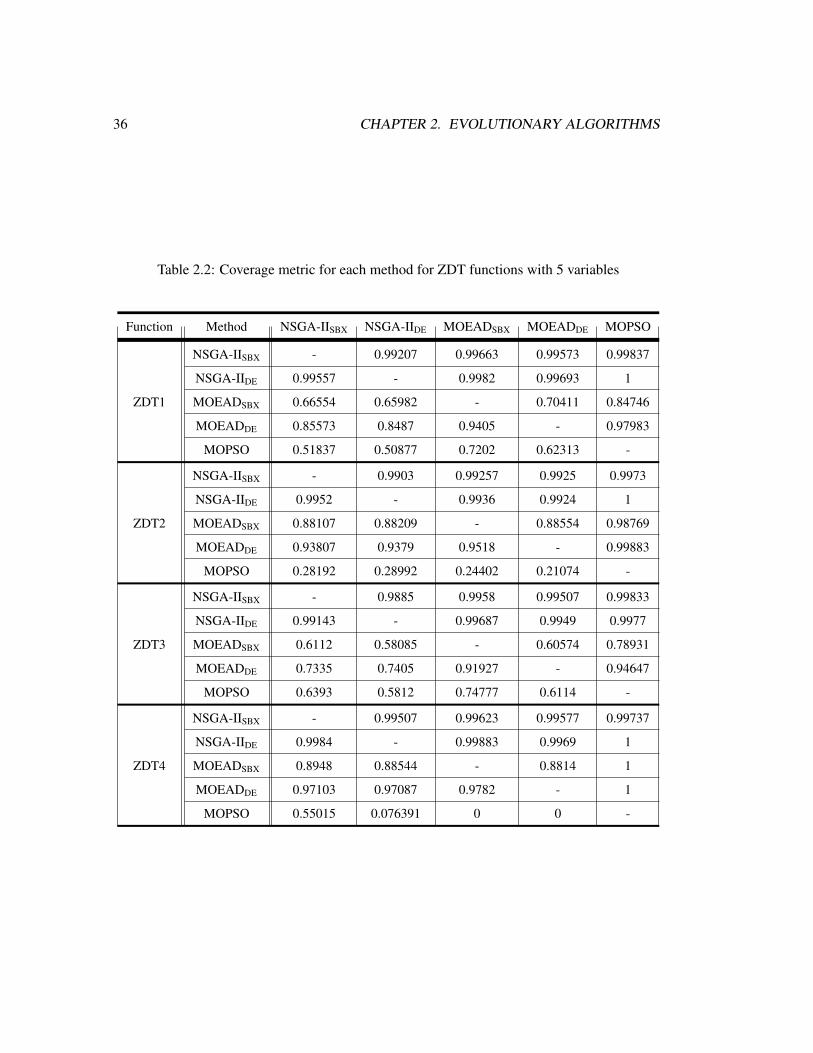
36 CHAPTER 2. EVOLUTIONARY ALGORITHMS
Table 2.2: Coverage metric for each method for ZDT functions with 5 variables
Function Method NSGA-IISBX NSGA-IIDE MOEADSBX MOEADDE MOPSO
ZDT1
NSGA-IISBX - 0.99207 0.99663 0.99573 0.99837
NSGA-IIDE 0.99557 - 0.9982 0.99693 1
MOEADSBX 0.66554 0.65982 - 0.70411 0.84746
MOEADDE 0.85573 0.8487 0.9405 - 0.97983
MOPSO 0.51837 0.50877 0.7202 0.62313 -
ZDT2
NSGA-IISBX - 0.9903 0.99257 0.9925 0.9973
NSGA-IIDE 0.9952 - 0.9936 0.9924 1
MOEADSBX 0.88107 0.88209 - 0.88554 0.98769
MOEADDE 0.93807 0.9379 0.9518 - 0.99883
MOPSO 0.28192 0.28992 0.24402 0.21074 -
ZDT3
NSGA-IISBX - 0.9885 0.9958 0.99507 0.99833
NSGA-IIDE 0.99143 - 0.99687 0.9949 0.9977
MOEADSBX 0.6112 0.58085 - 0.60574 0.78931
MOEADDE 0.7335 0.7405 0.91927 - 0.94647
MOPSO 0.6393 0.5812 0.74777 0.6114 -
ZDT4
NSGA-IISBX - 0.99507 0.99623 0.99577 0.99737
NSGA-IIDE 0.9984 - 0.99883 0.9969 1
MOEADSBX 0.8948 0.88544 - 0.8814 1
MOEADDE 0.97103 0.97087 0.9782 - 1
MOPSO 0.55015 0.076391 0 0 -
Chapter 3
Circuit Optimization
3.1 Introduction
This chapter is devoted to show the optimization process of analog integrated circuits by using
evolutionary algorithms. In the first section, the proposed optimization methodology framework
based on successive simulations linking a circuit simulator, is presented.
Next, it is analyzed the performance of NSGA-II and MOEAD with two different recombi-
nation operators: SBX and DE, through the optimization of two mixed-mode circuits each one
with different number of design variables and three objective functions. The chapter ends show-
ing the optimization of nine amplifiers all of them with different number of design variables and
eleven objective functions.
3.2 Optimization Methodology Framework
To perform circuit optimization, after an initialization procedure, it is necessary in each gen-
eration to evaluate the population by linking a circuit simulator and by modifying each design
variable (as transistor width, transistor length or bias sources), and collecting these results.
Next, the new population is generated form the best individuals (or non-dominated solutions).
This process continues until the current generation reaches the maximum number of generations
as shown in Fig. 3.1.
37
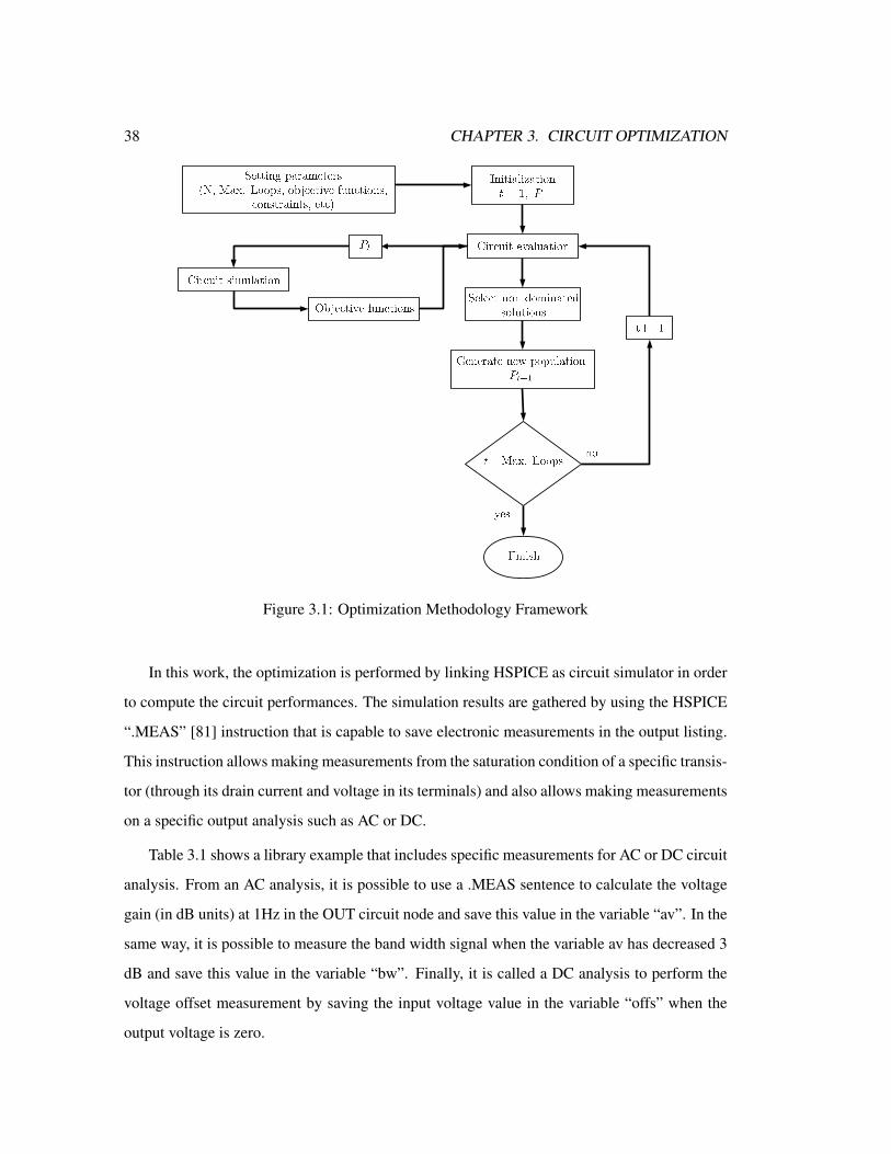
38 CHAPTER 3. CIRCUIT OPTIMIZATION
Figure 3.1: Optimization Methodology Framework
In this work, the optimization is performed by linking HSPICE as circuit simulator in order
to compute the circuit performances. The simulation results are gathered by using the HSPICE
“.MEAS” [81] instruction that is capable to save electronic measurements in the output listing.
This instruction allows making measurements from the saturation condition of a specific transis-
tor (through its drain current and voltage in its terminals) and also allows making measurements
on a specific output analysis such as AC or DC.
Table 3.1 shows a library example that includes specific measurements for AC or DC circuit
analysis. From an AC analysis, it is possible to use a .MEAS sentence to calculate the voltage
gain (in dB units) at 1Hz in the OUT circuit node and save this value in the variable “av”. In the
same way, it is possible to measure the band width signal when the variable av has decreased 3
dB and save this value in the variable “bw”. Finally, it is called a DC analysis to perform the
voltage offset measurement by saving the input voltage value in the variable “offs” when the
output voltage is zero.
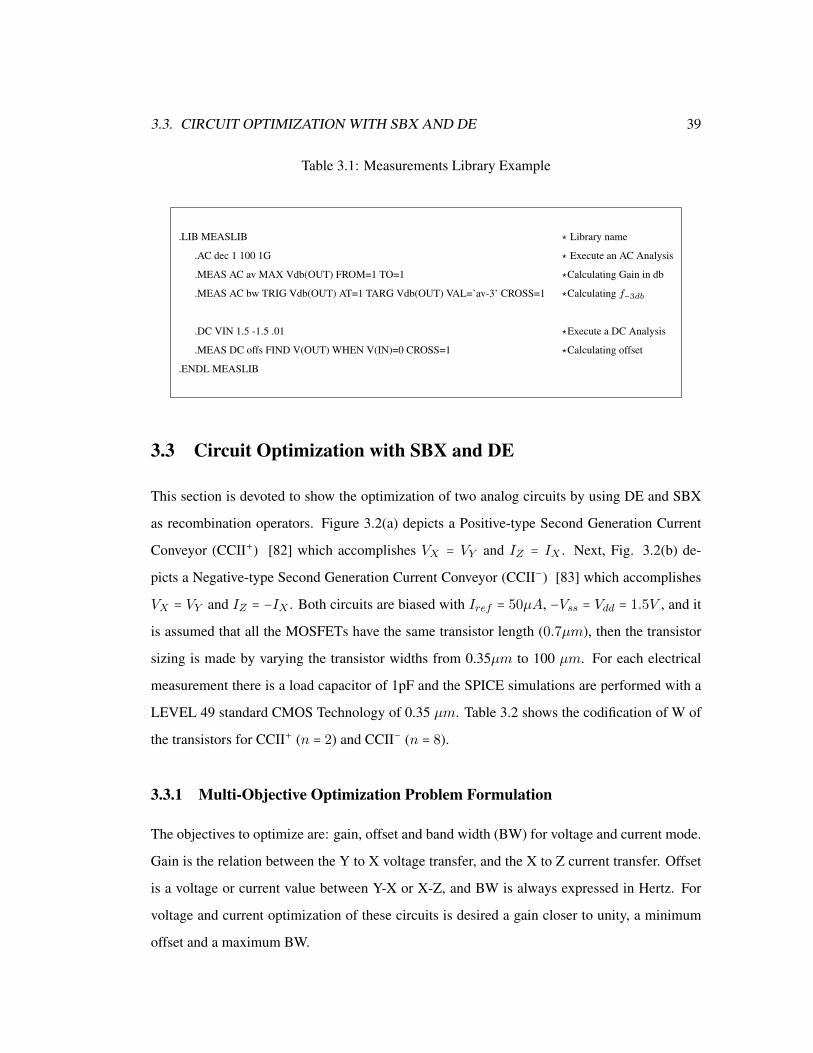
3.3. CIRCUIT OPTIMIZATION WITH SBX AND DE 39
Table 3.1: Measurements Library Example
.LIB MEASLIB ⋆ Library name
.AC dec 1 100 1G ⋆ Execute an AC Analysis
.MEAS AC av MAX Vdb(OUT) FROM=1 TO=1 ⋆Calculating Gain in db
.MEAS AC bw TRIG Vdb(OUT) AT=1 TARG Vdb(OUT) VAL=’av-3’ CROSS=1 ⋆Calculating f−3db
.DC VIN 1.5 -1.5 .01 ⋆Execute a DC Analysis
.MEAS DC offs FIND V(OUT) WHEN V(IN)=0 CROSS=1 ⋆Calculating offset
.ENDL MEASLIB
3.3 Circuit Optimization with SBX and DE
This section is devoted to show the optimization of two analog circuits by using DE and SBX
as recombination operators. Figure 3.2(a) depicts a Positive-type Second Generation Current
Conveyor (CCII+) [82] which accomplishes VX = VY and IZ = IX . Next, Fig. 3.2(b) de-
picts a Negative-type Second Generation Current Conveyor (CCII−) [83] which accomplishes
VX = VY and IZ = −IX . Both circuits are biased with Iref = 50µA, −Vss = Vdd = 1.5V , and it
is assumed that all the MOSFETs have the same transistor length (0.7µm), then the transistor
sizing is made by varying the transistor widths from 0.35µm to 100 µm. For each electrical
measurement there is a load capacitor of 1pF and the SPICE simulations are performed with a
LEVEL 49 standard CMOS Technology of 0.35 µm. Table 3.2 shows the codification of W of
the transistors for CCII+ (n = 2) and CCII− (n = 8).
3.3.1 Multi-Objective Optimization Problem Formulation
The objectives to optimize are: gain, offset and band width (BW) for voltage and current mode.
Gain is the relation between the Y to X voltage transfer, and the X to Z current transfer. Offset
is a voltage or current value between Y-X or X-Z, and BW is always expressed in Hertz. For
voltage and current optimization of these circuits is desired a gain closer to unity, a minimum
offset and a maximum BW.
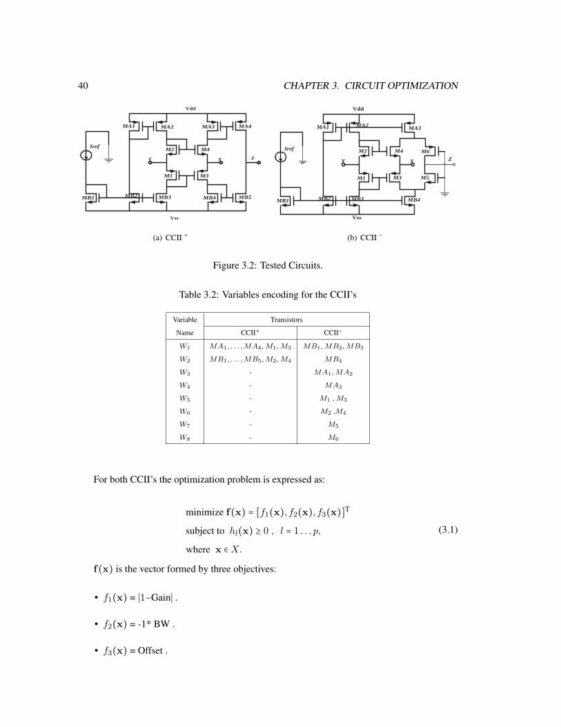
40 CHAPTER 3. CIRCUIT OPTIMIZATION
M1
Iref
Vdd
MA1
MB1 MB2 MB3
M4 M2
Y
MA3 MA2
M3
MB4
X Z
f MA4
MB5
Vss
(a) CCII +
M1
Iref
Vdd
MA1
MB1 MB2 MB3
M4 M2
Y
M6
MA2
M3 M5
X Z
MA3
MB4
Vss
(b) CCII −
Figure 3.2: Tested Circuits.
Table 3.2: Variables encoding for the CCII’s
Variable Transistors
Name CCII+ CCII−
W1 MA1, . . . ,MA4, M1, M3 MB1, MB2, MB3
W2 MB1, . . . ,MB5, M2, M4 MB4
W3 - MA1, MA2
W4 - MA3
W5 - M1 , M3
W6 - M2 ,M4
W7 - M5
W8 - M6
For both CCII’s the optimization problem is expressed as:
minimize f(x) = [f1(x), f2(x), f3(x)]T
subject to hl(x) ≥ 0 , l = 1 . . . p,
where x ∈X.
(3.1)
f(x) is the vector formed by three objectives:
• f1(x) = ∣1−Gain∣ .
• f2(x) = -1* BW .
• f3(x) = Offset .
3.3. CIRCUIT OPTIMIZATION WITH SBX AND DE 41
where X ∶ Rn ∣ 0.35 µm ≤ Wi ≤ 100 µm is the decision space (X) for the n variables.
Finally, hl(x), l = 1 . . . p are performance constraints, in our experiments we include the next
constraints:
• The saturation condition in all transistors.
• ∣1−Gain∣ < 0.1.
• BW > 100MHz.
• Voltage offset < 1mV .
• Current offset < 1µA .
3.3.2 Results
The circuits are optimized along 10 runs (in a dual processor 2GHz, RAM 2GHz). For CCII+
it was selected N=80 (H = 12 for MOEAD) along 80 generations. For CCII− it was selected
N =152 (H = 17 for MOEAD) along 200 generations.
Figures 3.3 - 3.4 depict the last non-dominated solutions for voltage and current optimiza-
tion for the NSGA-II and MOEAD approaches for the CCII+ along 10 runs, herein the Pareto
fronts of these experiments are similar.
Tables 3.3 and 3.4 show the worst, mean and best objective values found by each method
as result of the optimization of both circuits. Among all these results it is bear out that the
constraints of gain, band width and offset were accomplished in voltage and current mode. The
loop time is comparable for all the experiments, only MOEADDE particulary preserves always
the less mean time.
Regarding to the voltage optimization for the CCII+, both NSGA-II experiments achieved
similar objective values between NSGA-IISBX and NSGA-IIDE. Both MOEAD experiments
also have similar objective values between MOEADSBX and MOEADDE . The average differ-
ence among all the experiments for the voltage optimization of CCII+ is 3% (left side of Table
3.3).
For the current optimization of the CCII+, the NSGA-II experiments found the same best,
worst and mean objective values and the MOEAD experiments have similar objective values.
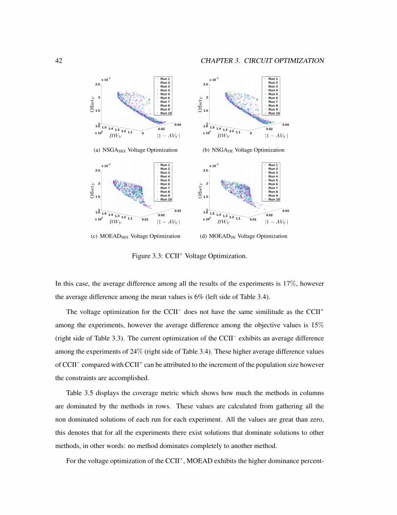
42 CHAPTER 3. CIRCUIT OPTIMIZATION
00.02
0.04
1.11.21.31.41.51.6
x 108
1
1.5
2
2.5x 10
−3
|1 − AVY |BWY
Offset Y
Run 1Run 2Run 3Run 4Run 5Run 6Run 7Run 8Run 9Run 10
(a) NSGASBX Voltage Optimization
00.02
0.04
1.11.21.31.41.51.6
x 108
1
1.5
2
2.5x 10
−3
|1 − AVY |BWY
Offset Y
Run 1Run 2Run 3Run 4Run 5Run 6Run 7Run 8Run 9Run 10
(b) NSGADE Voltage Optimization
0.010.02
0.03
1.11.21.31.41.51.6
x 108
1
1.5
2
2.5x 10
−3
|1 − AVY |BWY
Offset Y
Run 1Run 2Run 3Run 4Run 5Run 6Run 7Run 8Run 9Run 10
(c) MOEADSBX Voltage Optimization
0.010.02
0.03
1.11.21.31.41.51.6
x 108
1
1.5
2
2.5x 10
−3
|1 − AVY |BWY
Offset Y
Run 1Run 2Run 3Run 4Run 5Run 6Run 7Run 8Run 9Run 10
(d) MOEADDE Voltage Optimization
Figure 3.3: CCII+ Voltage Optimization.
In this case, the average difference among all the results of the experiments is 17%, however
the average difference among the mean values is 6% (left side of Table 3.4).
The voltage optimization for the CCII− does not have the same similitude as the CCII+
among the experiments, however the average difference among the objective values is 15%
(right side of Table 3.3). The current optimization of the CCII− exhibits an average difference
among the experiments of 24% (right side of Table 3.4). These higher average difference values
of CCII− compared with CCII+ can be attributed to the increment of the population size however
the constraints are accomplished.
Table 3.5 displays the coverage metric which shows how much the methods in columns
are dominated by the methods in rows. These values are calculated from gathering all the
non dominated solutions of each run for each experiment. All the values are great than zero,
this denotes that for all the experiments there exist solutions that dominate solutions to other
methods, in other words: no method dominates completely to another method.
For the voltage optimization of the CCII+, MOEAD exhibits the higher dominance percent-
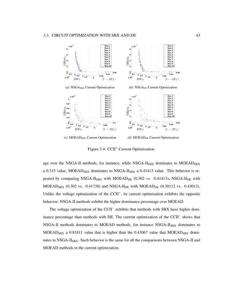
3.3. CIRCUIT OPTIMIZATION WITH SBX AND DE 43
00.02
0.040.06
1.522.533.54
x 108
0
2
4
6
8x 10
−7
|1 − AVY |BWY
Offset Y
Run 1Run 2Run 3Run 4Run 5Run 6Run 7Run 8Run 9Run 10
(a) NSGASBX Current Optimization
00.02
0.040.06
1.522.533.54
x 108
0
2
4
6
8x 10
−7
|1 − AVY |BWY
Offset Y
Run 1Run 2Run 3Run 4Run 5Run 6Run 7Run 8Run 9Run 10
(b) NSGADE Current Optimization
00.05
0.1
1.522.533.54
x 108
0
0.2
0.4
0.6
0.8
1x 10
−6
|1 − AVY |BWY
Offset Y
Run 1Run 2Run 3Run 4Run 5Run 6Run 7Run 8Run 9Run 10
(c) MOEADSBX Current Optimization
00.02
0.040.06
1.522.533.54
x 108
0
2
4
6
8x 10
−7
|1 − AVY |BWY
Offset Y
Run 1Run 2Run 3Run 4Run 5Run 6Run 7Run 8Run 9Run 10
(d) MOEADDE Current Optimization
Figure 3.4: CCII+ Current Optimization.
age over the NSGA-II methods, for instance, while NSGA-IISBX dominates to MOEADSBX
a 0.315 value, MOEADSBX dominates to NSGA-IISBX a 0.41413 value. This behavior is re-
peated by comparing NSGA-IISBX with MOEADDE (0.302 vs. 0.41413), NSGA-IIDE with
MOEADSBX (0.302 vs. 0.41738) and NSGA-IIDE with MOEADDE (0.30112 vs. 0.43013).
Unlike the voltage optimization of the CCII+, its current optimization exhibits the opposite
behavior: NSGA-II methods exhibit the higher dominance percentage over MOEAD.
The voltage optimization of the CCII− exhibits that methods with SBX have higher dom-
inance percentage than methods with DE. The current optimization of the CCII− shows that
NSGA-II methods dominates to MOEAD methods, for instance NSGA-IISBX dominates to
MOEADSBX a 0.81811 value that is higher than the 0.43067 value that MOEADSBX domi-
nates to NSGA-IISBX. Such behavior is the same for all the comparisons between NSGA-II and
MOEAD methods in the current optimization.
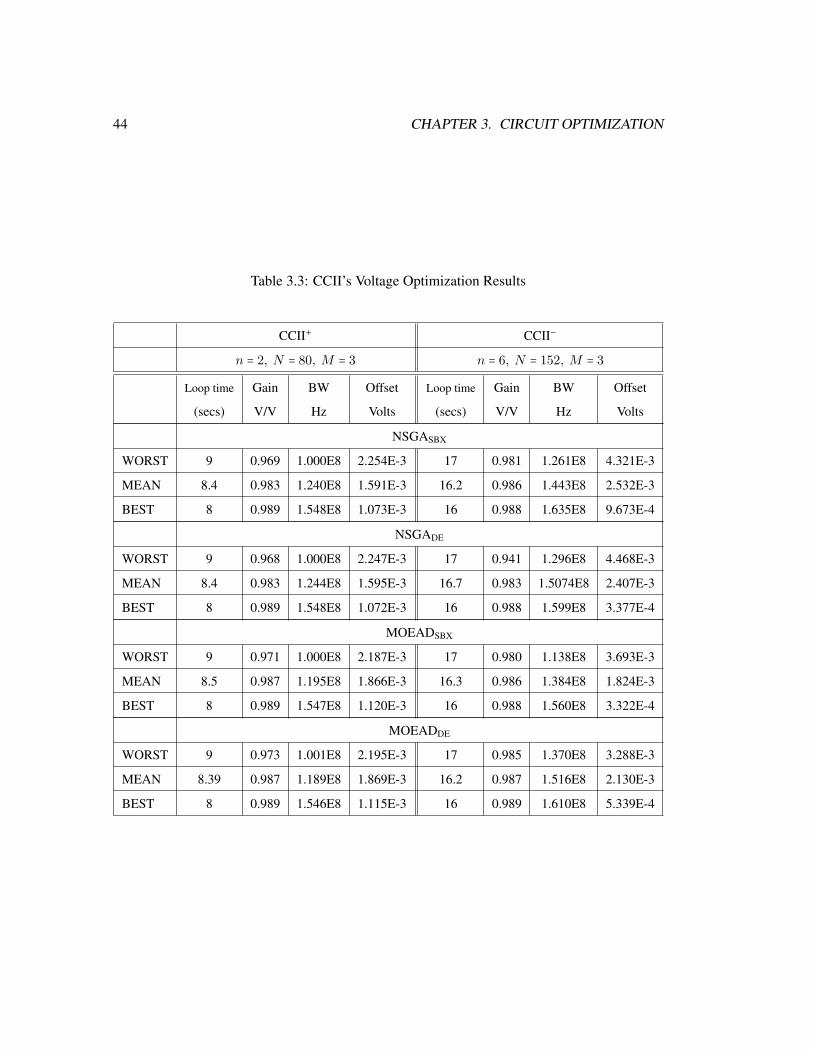
44 CHAPTER 3. CIRCUIT OPTIMIZATION
Table 3.3: CCII’s Voltage Optimization Results
CCII+ CCII−
n = 2, N = 80, M = 3 n = 6, N = 152, M = 3
Loop time Gain BW Offset Loop time Gain BW Offset
(secs) V/V Hz Volts (secs) V/V Hz Volts
NSGASBX
WORST 9 0.969 1.000E8 2.254E-3 17 0.981 1.261E8 4.321E-3
MEAN 8.4 0.983 1.240E8 1.591E-3 16.2 0.986 1.443E8 2.532E-3
BEST 8 0.989 1.548E8 1.073E-3 16 0.988 1.635E8 9.673E-4
NSGADE
WORST 9 0.968 1.000E8 2.247E-3 17 0.941 1.296E8 4.468E-3
MEAN 8.4 0.983 1.244E8 1.595E-3 16.7 0.983 1.5074E8 2.407E-3
BEST 8 0.989 1.548E8 1.072E-3 16 0.988 1.599E8 3.377E-4
MOEADSBX
WORST 9 0.971 1.000E8 2.187E-3 17 0.980 1.138E8 3.693E-3
MEAN 8.5 0.987 1.195E8 1.866E-3 16.3 0.986 1.384E8 1.824E-3
BEST 8 0.989 1.547E8 1.120E-3 16 0.988 1.560E8 3.322E-4
MOEADDE
WORST 9 0.973 1.001E8 2.195E-3 17 0.985 1.370E8 3.288E-3
MEAN 8.39 0.987 1.189E8 1.869E-3 16.2 0.987 1.516E8 2.130E-3
BEST 8 0.989 1.546E8 1.115E-3 16 0.989 1.610E8 5.339E-4
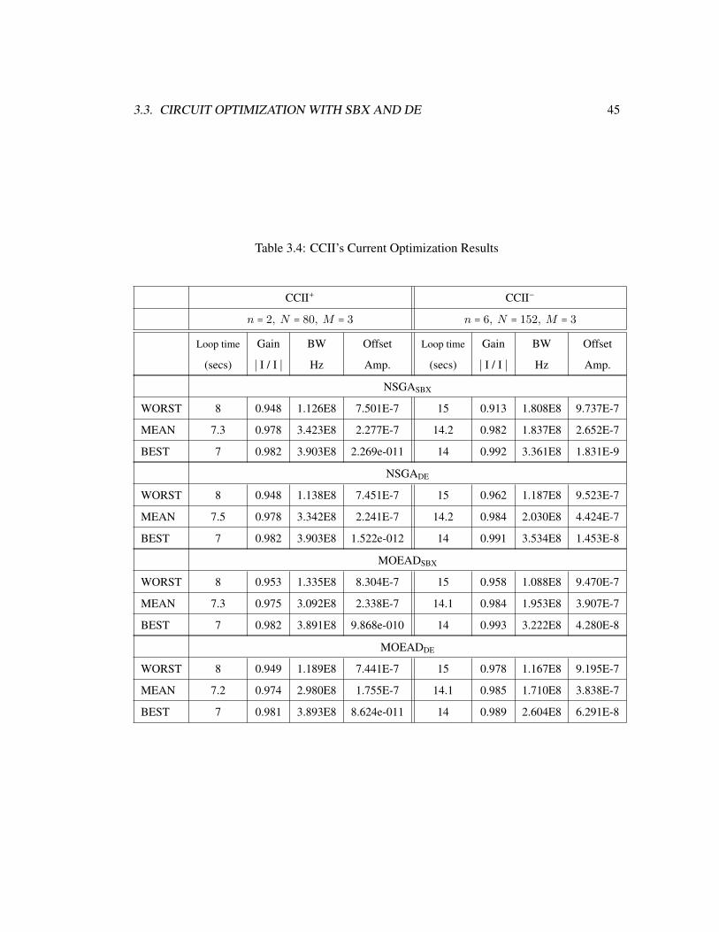
3.3. CIRCUIT OPTIMIZATION WITH SBX AND DE 45
Table 3.4: CCII’s Current Optimization Results
CCII+ CCII−
n = 2, N = 80, M = 3 n = 6, N = 152, M = 3
Loop time Gain BW Offset Loop time Gain BW Offset
(secs) ∣ I / I ∣ Hz Amp. (secs) ∣ I / I ∣ Hz Amp.
NSGASBX
WORST 8 0.948 1.126E8 7.501E-7 15 0.913 1.808E8 9.737E-7
MEAN 7.3 0.978 3.423E8 2.277E-7 14.2 0.982 1.837E8 2.652E-7
BEST 7 0.982 3.903E8 2.269e-011 14 0.992 3.361E8 1.831E-9
NSGADE
WORST 8 0.948 1.138E8 7.451E-7 15 0.962 1.187E8 9.523E-7
MEAN 7.5 0.978 3.342E8 2.241E-7 14.2 0.984 2.030E8 4.424E-7
BEST 7 0.982 3.903E8 1.522e-012 14 0.991 3.534E8 1.453E-8
MOEADSBX
WORST 8 0.953 1.335E8 8.304E-7 15 0.958 1.088E8 9.470E-7
MEAN 7.3 0.975 3.092E8 2.338E-7 14.1 0.984 1.953E8 3.907E-7
BEST 7 0.982 3.891E8 9.868e-010 14 0.993 3.222E8 4.280E-8
MOEADDE
WORST 8 0.949 1.189E8 7.441E-7 15 0.978 1.167E8 9.195E-7
MEAN 7.2 0.974 2.980E8 1.755E-7 14.1 0.985 1.710E8 3.838E-7
BEST 7 0.981 3.893E8 8.624e-011 14 0.989 2.604E8 6.291E-8
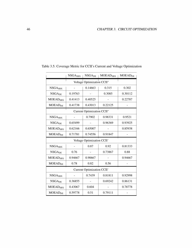
46 CHAPTER 3. CIRCUIT OPTIMIZATION
Table 3.5: Coverage Metric for CCII’s Current and Voltage Optimization
NSGASBX NSGADE MOEADSBX MOEADDE
Voltage Optimization CCII+
NSGASBX - 0.14663 0.315 0.302
NSGADE 0.19763 - 0.3085 0.30112
MOEADSBX 0.41413 0.40525 - 0.22787
MOEADDE 0.41738 0.43013 0.22125 -
Current Optimization CCII+
NSGASBX - 0.7902 0.98331 0.9521
NSGADE 0.65499 - 0.96369 0.93925
MOEADSBX 0.62166 0.65007 - 0.85938
MOEADDE 0.71781 0.74556 0.91847 -
Voltage Optimization CCII−
NSGASBX - 0.87 0.92 0.81333
NSGADE 0.76 - 0.73867 0.88
MOEADSBX 0.94667 0.90667 - 0.94667
MOEADDE 0.78 0.82 0.56 -
Current Optimization CCII−
NSGASBX - 0.7439 0.81811 0.92998
NSGADE 0.36855 - 0.69242 0.86131
MOEADSBX 0.43067 0.604 - 0.78778
MOEADDE 0.59778 0.51 0.79111 -
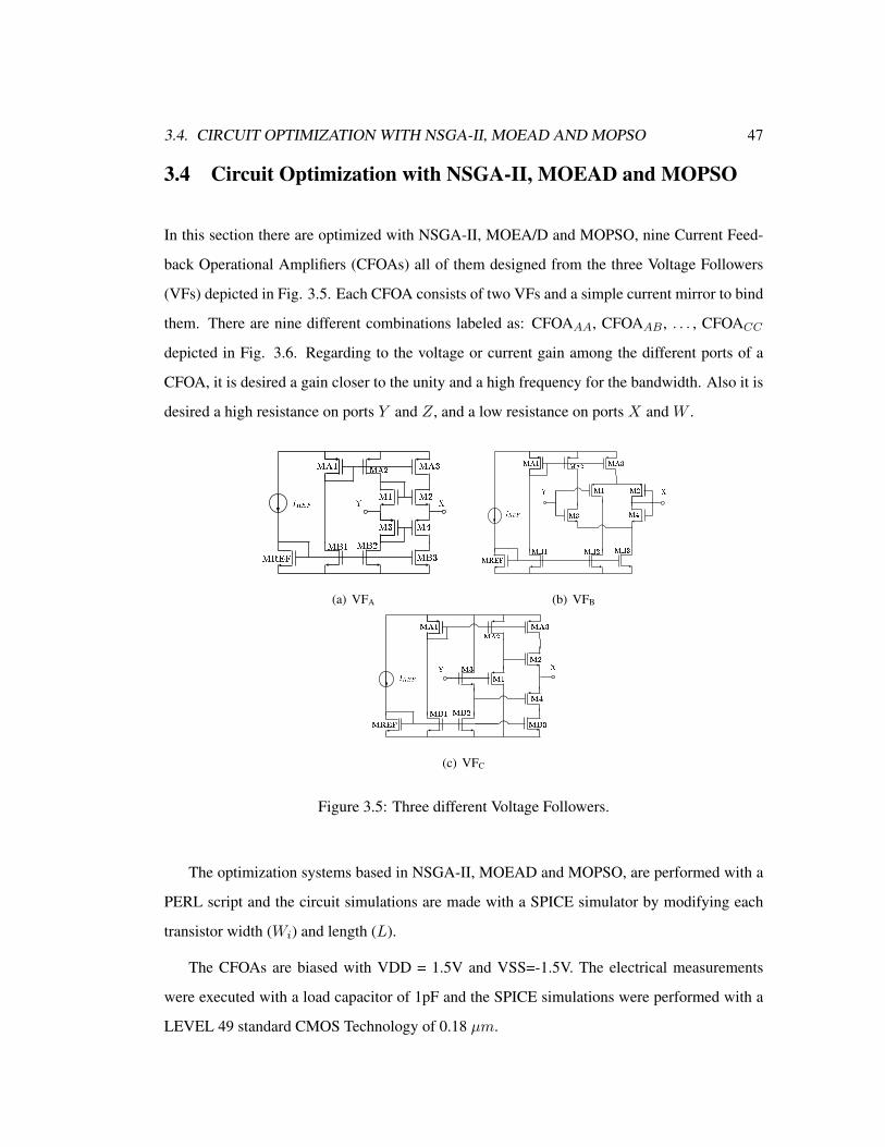
3.4. CIRCUIT OPTIMIZATION WITH NSGA-II, MOEAD AND MOPSO 47
3.4 Circuit Optimization with NSGA-II, MOEAD and MOPSO
In this section there are optimized with NSGA-II, MOEA/D and MOPSO, nine Current Feed-
back Operational Amplifiers (CFOAs) all of them designed from the three Voltage Followers
(VFs) depicted in Fig. 3.5. Each CFOA consists of two VFs and a simple current mirror to bind
them. There are nine different combinations labeled as: CFOAAA, CFOAAB , . . . , CFOACC
depicted in Fig. 3.6. Regarding to the voltage or current gain among the different ports of a
CFOA, it is desired a gain closer to the unity and a high frequency for the bandwidth. Also it is
desired a high resistance on ports Y and Z, and a low resistance on ports X and W .
(a) VFA (b) VFB
(c) VFC
Figure 3.5: Three different Voltage Followers.
The optimization systems based in NSGA-II, MOEAD and MOPSO, are performed with a
PERL script and the circuit simulations are made with a SPICE simulator by modifying each
transistor width (Wi) and length (L).
The CFOAs are biased with VDD = 1.5V and VSS=-1.5V. The electrical measurements
were executed with a load capacitor of 1pF and the SPICE simulations were performed with a
LEVEL 49 standard CMOS Technology of 0.18 µm.
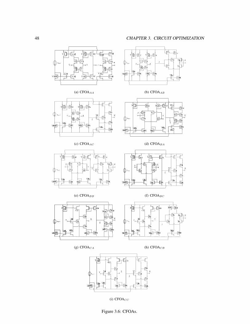
48 CHAPTER 3. CIRCUIT OPTIMIZATION
(a) CFOAAA (b) CFOAAB
(c) CFOAAC (d) CFOABA
(e) CFOABB (f) CFOABC
(g) CFOACA (h) CFOACB
(i) CFOACC
Figure 3.6: CFOAs.
3.4. CIRCUIT OPTIMIZATION WITH NSGA-II, MOEAD AND MOPSO 49
All CFOAs are encoded with transistors lengths (Li) and widths (Wi), where i represents
a specific transistor (or transistors which share the same length or/and width ) of the circuit.
The decision space for L is 0.18µm ≤ L ≤ 0.9µm, for W is 0.18µm ≤ L ≤ 200µm. All L
and W values are rounded to multiples of the minimum allowed by the technology process,
because besides the simulator can not handle continuous values, the scaling process to other
technologies can be done easily. Besides Ls and W s, there exists one more variable for IREF
which decision space is 10µA ≤ IREF ≤ 400µA. The variables encoding for each CFOA are
listed in Tables 3.6 to 3.14, where are the variables assigned for the different transistors and the
current variable IREF .
3.4.1 Multi-Objective Optimization Problem Formulation
For all CFOAs the optimization problem is expressed as:
minimize f(x) = [f1(x), f2(x), . . . , f11(x)]T
subject to hl(x) ≥ 0 , l = 1 . . . p,
where x ∈X.
(3.2)
f(x) is the vector formed by eleven objectives:
• f1(x) = Power consumption .
• f2(x) = ∣1 - Voltage gain from Y port to X port∣ (GAINX ).
• f3(x) = -1* Voltage band width from Y port to X port (BWX ).
• f4(x) = -1* Input resistance on Y port (ZY ).
• f5(x) = Output resistance on X port (ZX ).
• f6(x) = ∣ 1 - Current gain from X port to Z port∣ (GAINZ).
• f7(x) = -1* Current band width from X port to Z port (BWZ).
• f8(x) = -1* Output resistance on Z port (ZZ).
• f9(x) = ∣1 - Voltage gain from Z port to W port∣ (GAINW ).
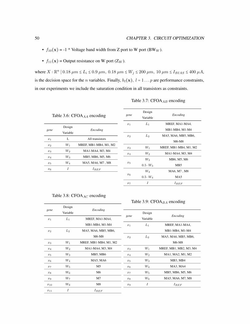
50 CHAPTER 3. CIRCUIT OPTIMIZATION
• f10(x) = -1 * Voltage band width from Z port to W port (BWW ).
• f11(x) = Output resistance on W port (ZW ).
where X ∶ Rn ∣ 0.18 µm ≤ Li ≤ 0.9 µm, 0.18 µm ≤Wj ≤ 200 µm, 10 µm ≤ IBIAS ≤ 400 µA,
is the decision space for the n variables. Finally, hl(x), l = 1 . . . p are performance constraints,
in our experiments we include the saturation condition in all transistors as constraints.
Table 3.6: CFOAAA encoding
geneDesign
EncodingVariable
x1 L All transistors
x2 W1 MREF, MB1-MB4, M1, M2
x3 W2 MA1-MA4, M3, M4
x4 W3 MB5, MB6, M5, M6
x5 W4 MA5, MA6, M7 , M8
x6 I IREF
Table 3.7: CFOAAB encoding
geneDesign
EncodingVariable
x1 L1 MREF, MA1-MA4,
MB1-MB4, M1-M4
x2 L2 MA5, MA6, MB5, MB6,
M6-M8
x3 W1 MREF, MB1-MB4, M1, M2
x4 W2 MA1-MA4, M3, M4
x5W3 MB6, M5, M6
0.5 ⋅W3 MB5
x6W4 MA6, M7 , M8
0.5 ⋅W4 MA5
x7 I IREF
Table 3.8: CFOAAC encoding
geneDesign
EncodingVariable
x1 L1 MREF, MA1-MA4,
MB1-MB4, M1-M4
x2 L2 MA5, MA6, MB5, MB6,
M6-M8
x3 W1 MREF, MB1-MB4, M1, M2
x4 W2 MA1-MA4, M3, M4
x5 W3 MB5, MB6
x6 W4 MA5, MA6
x7 W5 M5
x8 W6 M6
x9 W7 M7
x10 W8 M8
x11 I IREF
Table 3.9: CFOABA encoding
geneDesign
EncodingVariable
x1 L1 MREF, MA1-MA4,
MB1-MB4, M1-M4
x2 L2 MA5, MA6, MB5, MB6,
M6-M8
x3 W1 MREF, MB1, MB2, M3, M4
x4 W2 MA1, MA2, M1, M2
x5 W3 MB3, MB4
x6 W4 MA3, MA4
x7 W5 MB5, MB6, M5, M6
x8 W6 MA5, MA6, M7, M8
x9 I IREF
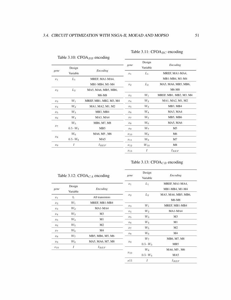
3.4. CIRCUIT OPTIMIZATION WITH NSGA-II, MOEAD AND MOPSO 51
Table 3.10: CFOABB encoding
geneDesign
EncodingVariable
x1 L1 MREF, MA1-MA4,
MB1-MB4, M1-M4
x2 L2 MA5, MA6, MB5, MB6,
M6-M8
x3 W1 MREF, MB1, MB2, M3, M4
x4 W2 MA1, MA2, M1, M2
x5 W3 MB3, MB4
x6 W4 MA3, MA4
x7W5 MB6, M7, M8
0.5 ⋅W5 MB5
x8W6 MA6, M5 , M6
0.5 ⋅W6 MA5
x9 I IREF
Table 3.11: CFOABC encoding
geneDesign
EncodingVariable
x1 L1 MREF, MA1-MA4,
MB1-MB4, M1-M4
x2 L2 MA5, MA6, MB5, MB6,
M6-M8
x3 W1 MREF, MB1, MB2, M3, M4
x4 W2 MA1, MA2, M1, M2
x5 W3 MB3, MB4
x6 W4 MA3, MA4
x7 W5 MB5, MB6
x8 W6 MA5, MA6
x9 W7 M5
x10 W8 M6
x11 W9 M7
x12 W10 M8
x13 I IREF
Table 3.12: CFOACA encoding
geneDesign
EncodingVariable
x1 L All transistors
x2 W1 MREF, MB1-MB4
x3 W2 MA1-MA4
x4 W3 M3
x5 W4 M1
x6 W5 M2
x7 W6 M4
x8 W7 MB5, MB6, M5, M6
x9 W8 MA5, MA6, M7, M8
x10 I IREF
Table 3.13: CFOACB encoding
geneDesign
EncodingVariable
x1 L1 MREF, MA1-MA4,
MB1-MB4, M1-M4
x2 L2 MA5, MA6, MB5, MB6,
M6-M8
x3 W1 MREF, MB1-MB4
x4 W2 MA1-MA4
x5 W3 M3
x6 W4 M1
x7 W5 M2
x8 W6 M4
x9W7 MB6, M7, M8
0.5 ⋅W3 MB5
x10W8 MA6, M5 , M6
0.5 ⋅W4 MA5
x11 I IREF
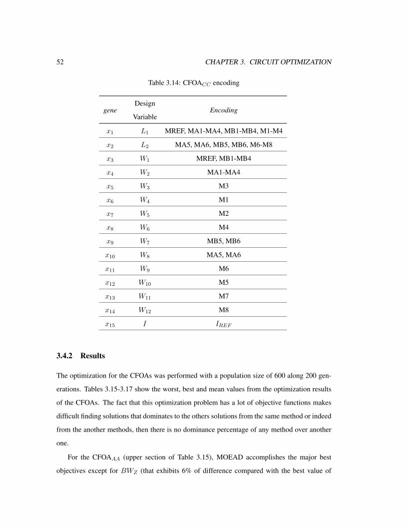
52 CHAPTER 3. CIRCUIT OPTIMIZATION
Table 3.14: CFOACC encoding
geneDesign
EncodingVariable
x1 L1 MREF, MA1-MA4, MB1-MB4, M1-M4
x2 L2 MA5, MA6, MB5, MB6, M6-M8
x3 W1 MREF, MB1-MB4
x4 W2 MA1-MA4
x5 W3 M3
x6 W4 M1
x7 W5 M2
x8 W6 M4
x9 W7 MB5, MB6
x10 W8 MA5, MA6
x11 W9 M6
x12 W10 M5
x13 W11 M7
x14 W12 M8
x15 I IREF
3.4.2 Results
The optimization for the CFOAs was performed with a population size of 600 along 200 gen-
erations. Tables 3.15-3.17 show the worst, best and mean values from the optimization results
of the CFOAs. The fact that this optimization problem has a lot of objective functions makes
difficult finding solutions that dominates to the others solutions from the same method or indeed
from the another methods, then there is no dominance percentage of any method over another
one.
For the CFOAAA (upper section of Table 3.15), MOEAD accomplishes the major best
objectives except for BWZ (that exhibits 6% of difference compared with the best value of

3.4. CIRCUIT OPTIMIZATION WITH NSGA-II, MOEAD AND MOPSO 53
NSGA-II) and GAINW (that exhibits less than 1% compared with the best value of NSGA-
II). With the CFOAAB optimization (mid section of Table 3.15), MOEAD achieved the best
values of each objective function compared with the other methods. In the optimization of the
CFOAAC (lower section of the Table 3.15), again MOEAD has the best objective values except
for power consumption (with a difference of 15% compared with the best NSGA-II value) and
GAINW (with a difference less than 1% compared with the best MOPSO value).
In the CFOABA optimization (upper section of Table 3.16), both NSGA-II and MOEAD
has the best vales, however, despite MOEAD achieved one best value than NSGA-II, this last
exhibits the best value for the power consumption. The optimization of CFOABB (mid section
of Table 3.16) is led by MOEAD, but different to the previous circuits, PSO achieved best
values than NSGA-II. With the CFOABC (lower section of Table 3.16), MOEAD exhibit the
best objective values, followed by NSGA-II and sometimes MOPSO provides better values than
NSGA-II (in ZX , BWZ , BWW and ZW ).
The optimization of the CFOACA, CFOACB and CFOACC (Table 3.17) is completely led
by MOEAD followed by NSGA-II and finally by MOPSO.
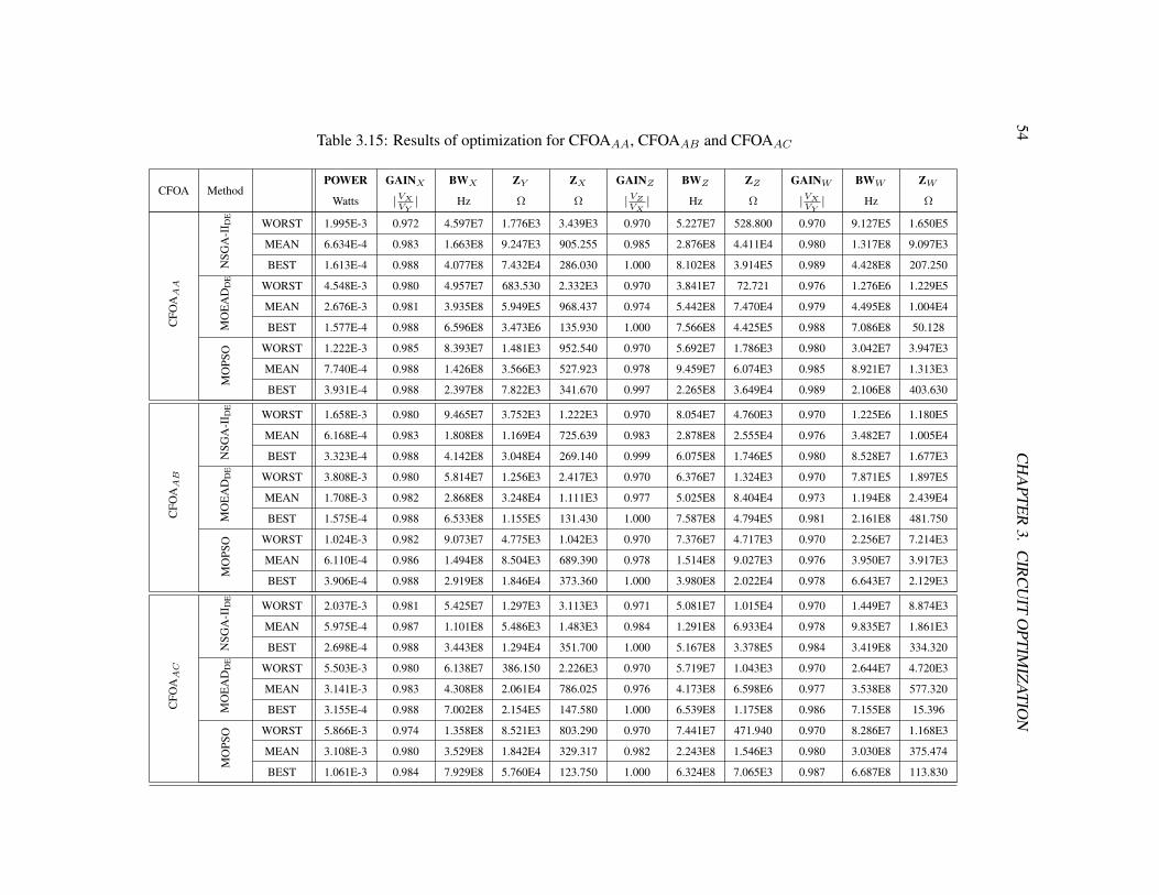
54C
HA
PTE
R3.
CIR
CU
ITO
PTIM
IZA
TIO
NTable 3.15: Results of optimization for CFOAAA, CFOAAB and CFOAAC
CFOA MethodPOWER GAINX BWX ZY ZX GAINZ BWZ ZZ GAINW BWW ZW
Watts ∣VXVY∣ Hz Ω Ω ∣ VZ
VX∣ Hz Ω ∣VX
VY∣ Hz Ω
CFO
AAA
NSG
A-I
I DE
WORST 1.995E-3 0.972 4.597E7 1.776E3 3.439E3 0.970 5.227E7 528.800 0.970 9.127E5 1.650E5
MEAN 6.634E-4 0.983 1.663E8 9.247E3 905.255 0.985 2.876E8 4.411E4 0.980 1.317E8 9.097E3
BEST 1.613E-4 0.988 4.077E8 7.432E4 286.030 1.000 8.102E8 3.914E5 0.989 4.428E8 207.250
MO
EA
DD
E
WORST 4.548E-3 0.980 4.957E7 683.530 2.332E3 0.970 3.841E7 72.721 0.976 1.276E6 1.229E5
MEAN 2.676E-3 0.981 3.935E8 5.949E5 968.437 0.974 5.442E8 7.470E4 0.979 4.495E8 1.004E4
BEST 1.577E-4 0.988 6.596E8 3.473E6 135.930 1.000 7.566E8 4.425E5 0.988 7.086E8 50.128
MO
PSO WORST 1.222E-3 0.985 8.393E7 1.481E3 952.540 0.970 5.692E7 1.786E3 0.980 3.042E7 3.947E3
MEAN 7.740E-4 0.988 1.426E8 3.566E3 527.923 0.978 9.459E7 6.074E3 0.985 8.921E7 1.313E3
BEST 3.931E-4 0.988 2.397E8 7.822E3 341.670 0.997 2.265E8 3.649E4 0.989 2.106E8 403.630
CFO
AAB
NSG
A-I
I DE
WORST 1.658E-3 0.980 9.465E7 3.752E3 1.222E3 0.970 8.054E7 4.760E3 0.970 1.225E6 1.180E5
MEAN 6.168E-4 0.983 1.808E8 1.169E4 725.639 0.983 2.878E8 2.555E4 0.976 3.482E7 1.005E4
BEST 3.323E-4 0.988 4.142E8 3.048E4 269.140 0.999 6.075E8 1.746E5 0.980 8.528E7 1.677E3
MO
EA
DD
E
WORST 3.808E-3 0.980 5.814E7 1.256E3 2.417E3 0.970 6.376E7 1.324E3 0.970 7.871E5 1.897E5
MEAN 1.708E-3 0.982 2.868E8 3.248E4 1.111E3 0.977 5.025E8 8.404E4 0.973 1.194E8 2.439E4
BEST 1.575E-4 0.988 6.533E8 1.155E5 131.430 1.000 7.587E8 4.794E5 0.981 2.161E8 481.750
MO
PSO WORST 1.024E-3 0.982 9.073E7 4.775E3 1.042E3 0.970 7.376E7 4.717E3 0.970 2.256E7 7.214E3
MEAN 6.110E-4 0.986 1.494E8 8.504E3 689.390 0.978 1.514E8 9.027E3 0.976 3.950E7 3.917E3
BEST 3.906E-4 0.988 2.919E8 1.846E4 373.360 1.000 3.980E8 2.022E4 0.978 6.643E7 2.129E3
CFO
AAC
NSG
A-I
I DE
WORST 2.037E-3 0.981 5.425E7 1.297E3 3.113E3 0.971 5.081E7 1.015E4 0.970 1.449E7 8.874E3
MEAN 5.975E-4 0.987 1.101E8 5.486E3 1.483E3 0.984 1.291E8 6.933E4 0.978 9.835E7 1.861E3
BEST 2.698E-4 0.988 3.443E8 1.294E4 351.700 1.000 5.167E8 3.378E5 0.984 3.419E8 334.320
MO
EA
DD
E
WORST 5.503E-3 0.980 6.138E7 386.150 2.226E3 0.970 5.719E7 1.043E3 0.970 2.644E7 4.720E3
MEAN 3.141E-3 0.983 4.308E8 2.061E4 786.025 0.976 4.173E8 6.598E6 0.977 3.538E8 577.320
BEST 3.155E-4 0.988 7.002E8 2.154E5 147.580 1.000 6.539E8 1.175E8 0.986 7.155E8 15.396
MO
PSO WORST 5.866E-3 0.974 1.358E8 8.521E3 803.290 0.970 7.441E7 471.940 0.970 8.286E7 1.168E3
MEAN 3.108E-3 0.980 3.529E8 1.842E4 329.317 0.982 2.243E8 1.546E3 0.980 3.030E8 375.474
BEST 1.061E-3 0.984 7.929E8 5.760E4 123.750 1.000 6.324E8 7.065E3 0.987 6.687E8 113.830
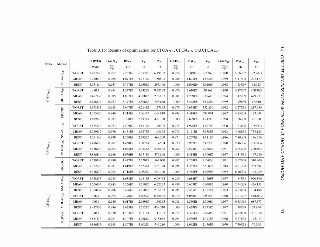
3.4.C
IRC
UIT
OPT
IMIZ
AT
ION
WIT
HN
SGA
-II,MO
EA
DA
ND
MO
PSO55
Table 3.16: Results of optimization for CFOABA, CFOABB and CFOABC
CFOA MethodPOWER GAINX BWX ZY ZX GAINZ BWZ ZZ GAINW BWW ZW
Watts ∣VXVY∣ Hz Ω Ω ∣ VZ
VX∣ Hz Ω ∣VX
VY∣ Hz Ω
CFO
ABA
NSG
A-I
I DE
WORST 9.102E-3 0.977 2.253E7 6.772E3 6.495E3 0.970 3.319E7 62.267 0.970 5.668E7 3.237E3
MEAN 2.760E-3 0.985 1.071E8 5.177E4 1.508E3 0.986 1.623E8 1.832E3 0.979 5.118E8 292.173
BEST 3.354E-4 0.987 3.767E8 3.030E6 295.400 1.000 1.090E9 3.026E4 0.988 1.335E9 34.123
MO
EA
DD
E
WORST 0.015 0.981 1.577E7 3.342E3 9.727E3 0.970 3.610E7 29.862 0.970 3.177E7 3.881E3
MEAN 8.462E-3 0.985 1.867E8 4.308E5 2.358E3 0.981 1.789E8 6.604E3 0.974 1.122E9 479.277
BEST 4.688E-4 0.987 3.377E8 2.568E6 255.830 1.000 5.448E8 5.892E4 0.989 1.991E9 16.510
MO
PSO WORST 8.973E-3 0.983 7.907E7 6.214E3 1.271E3 0.970 9.073E7 352.250 0.972 2.277E8 287.930
MEAN 4.375E-3 0.986 1.513E8 1.064E4 649.810 0.989 1.418E8 592.064 0.982 4.932E8 123.039
BEST 1.639E-3 0.987 2.300E8 2.197E4 429.100 1.000 2.629E8 1.242E3 0.988 1.269E9 46.300
CFO
ABB
NSG
A-I
I DE
WORST 6.835E-3 0.973 7.509E7 3.811E4 1.994E3 0.971 1.976E8 1.007E3 0.900 1.031E8 1.290E3
MEAN 5.769E-3 0.976 1.151E8 1.537E5 1.431E3 0.972 2.121E8 8.558E3 0.923 4.461E8 733.125
BEST 4.704E-3 0.979 1.550E8 2.693E5 869.200 0.974 2.267E8 1.611E4 0.946 7.890E8 176.550
MO
EA
DD
E
WORST 8.456E-3 0.981 1.450E7 1.087E4 1.065E4 0.970 3.987E7 539.720 0.970 5.463E6 2.579E4
MEAN 5.136E-3 0.983 1.044E8 6.354E5 3.360E3 0.982 9.573E7 2.288E4 0.971 2.657E8 2.385E3
BEST 3.866E-4 0.986 1.956E8 3.171E6 576.840 1.000 1.414E8 4.300E5 0.977 4.313E8 167.980
MO
PSO WORST 9.539E-3 0.980 1.477E8 2.220E4 864.060 0.987 1.238E8 410.030 0.921 3.074E8 510.400
MEAN 7.722E-3 0.981 1.619E8 2.523E4 775.178 0.996 1.357E8 627.022 0.944 4.012E8 283.694
BEST 6.746E-3 0.982 1.718E8 3.062E4 724.340 1.000 1.465E8 1.079E3 0.962 6.463E8 148.020
CFO
ABC
NSG
A-I
I DE
WORST 2.558E-3 0.985 1.633E7 1.131E5 9.094E3 0.980 4.084E7 2.470E3 0.977 1.643E8 920.390
MEAN 1.706E-3 0.985 3.256E7 5.510E5 6.323E3 0.986 5.603E7 6.049E3 0.980 2.740E8 456.133
BEST 8.760E-4 0.986 6.436E7 1.158E6 2.059E3 0.995 8.465E7 1.302E4 0.983 4.631E8 134.100
MO
EA
DD
E
WORST 0.023 0.972 2.178E7 8.405E3 6.880E3 0.970 5.088E7 425.590 0.970 3.077E7 4.665E3
MEAN 0.011 0.980 1.617E8 2.989E5 1.763E3 0.982 1.330E8 1.700E4 0.977 6.830E8 687.377
BEST 1.427E-3 0.986 2.623E8 1.712E6 438.310 1.000 2.429E8 1.173E5 0.987 1.387E9 27.954
MO
PSO WORST 0.011 0.978 1.133E8 3.311E4 1.117E3 0.979 1.325E8 850.450 0.971 4.321E8 281.310
MEAN 8.814E-3 0.981 1.307E8 4.088E4 915.685 0.994 1.536E8 1.373E3 0.976 5.271E8 145.413
BEST 6.886E-3 0.983 1.507E8 5.603E4 749.280 1.000 1.962E8 2.436E3 0.979 7.599E8 79.365
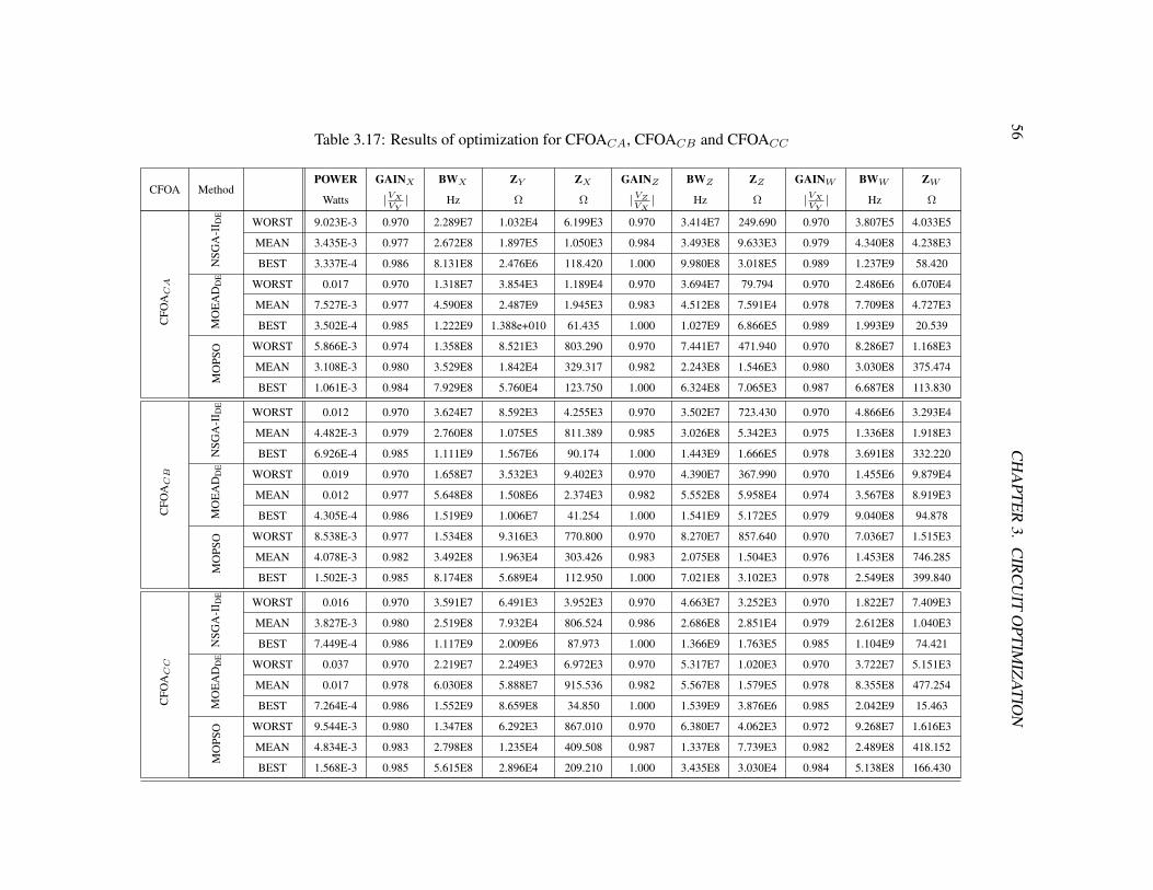
56C
HA
PTE
R3.
CIR
CU
ITO
PTIM
IZA
TIO
NTable 3.17: Results of optimization for CFOACA, CFOACB and CFOACC
CFOA MethodPOWER GAINX BWX ZY ZX GAINZ BWZ ZZ GAINW BWW ZW
Watts ∣VXVY∣ Hz Ω Ω ∣ VZ
VX∣ Hz Ω ∣VX
VY∣ Hz Ω
CFO
ACA
NSG
A-I
I DE
WORST 9.023E-3 0.970 2.289E7 1.032E4 6.199E3 0.970 3.414E7 249.690 0.970 3.807E5 4.033E5
MEAN 3.435E-3 0.977 2.672E8 1.897E5 1.050E3 0.984 3.493E8 9.633E3 0.979 4.340E8 4.238E3
BEST 3.337E-4 0.986 8.131E8 2.476E6 118.420 1.000 9.980E8 3.018E5 0.989 1.237E9 58.420
MO
EA
DD
E
WORST 0.017 0.970 1.318E7 3.854E3 1.189E4 0.970 3.694E7 79.794 0.970 2.486E6 6.070E4
MEAN 7.527E-3 0.977 4.590E8 2.487E9 1.945E3 0.983 4.512E8 7.591E4 0.978 7.709E8 4.727E3
BEST 3.502E-4 0.985 1.222E9 1.388e+010 61.435 1.000 1.027E9 6.866E5 0.989 1.993E9 20.539
MO
PSO WORST 5.866E-3 0.974 1.358E8 8.521E3 803.290 0.970 7.441E7 471.940 0.970 8.286E7 1.168E3
MEAN 3.108E-3 0.980 3.529E8 1.842E4 329.317 0.982 2.243E8 1.546E3 0.980 3.030E8 375.474
BEST 1.061E-3 0.984 7.929E8 5.760E4 123.750 1.000 6.324E8 7.065E3 0.987 6.687E8 113.830
CFO
ACB
NSG
A-I
I DE
WORST 0.012 0.970 3.624E7 8.592E3 4.255E3 0.970 3.502E7 723.430 0.970 4.866E6 3.293E4
MEAN 4.482E-3 0.979 2.760E8 1.075E5 811.389 0.985 3.026E8 5.342E3 0.975 1.336E8 1.918E3
BEST 6.926E-4 0.985 1.111E9 1.567E6 90.174 1.000 1.443E9 1.666E5 0.978 3.691E8 332.220
MO
EA
DD
E
WORST 0.019 0.970 1.658E7 3.532E3 9.402E3 0.970 4.390E7 367.990 0.970 1.455E6 9.879E4
MEAN 0.012 0.977 5.648E8 1.508E6 2.374E3 0.982 5.552E8 5.958E4 0.974 3.567E8 8.919E3
BEST 4.305E-4 0.986 1.519E9 1.006E7 41.254 1.000 1.541E9 5.172E5 0.979 9.040E8 94.878
MO
PSO WORST 8.538E-3 0.977 1.534E8 9.316E3 770.800 0.970 8.270E7 857.640 0.970 7.036E7 1.515E3
MEAN 4.078E-3 0.982 3.492E8 1.963E4 303.426 0.983 2.075E8 1.504E3 0.976 1.453E8 746.285
BEST 1.502E-3 0.985 8.174E8 5.689E4 112.950 1.000 7.021E8 3.102E3 0.978 2.549E8 399.840
CFO
ACC
NSG
A-I
I DE
WORST 0.016 0.970 3.591E7 6.491E3 3.952E3 0.970 4.663E7 3.252E3 0.970 1.822E7 7.409E3
MEAN 3.827E-3 0.980 2.519E8 7.932E4 806.524 0.986 2.686E8 2.851E4 0.979 2.612E8 1.040E3
BEST 7.449E-4 0.986 1.117E9 2.009E6 87.973 1.000 1.366E9 1.763E5 0.985 1.104E9 74.421
MO
EA
DD
E
WORST 0.037 0.970 2.219E7 2.249E3 6.972E3 0.970 5.317E7 1.020E3 0.970 3.722E7 5.151E3
MEAN 0.017 0.978 6.030E8 5.888E7 915.536 0.982 5.567E8 1.579E5 0.978 8.355E8 477.254
BEST 7.264E-4 0.986 1.552E9 8.659E8 34.850 1.000 1.539E9 3.876E6 0.985 2.042E9 15.463
MO
PSO WORST 9.544E-3 0.980 1.347E8 6.292E3 867.010 0.970 6.380E7 4.062E3 0.972 9.268E7 1.616E3
MEAN 4.834E-3 0.983 2.798E8 1.235E4 409.508 0.987 1.337E8 7.739E3 0.982 2.489E8 418.152
BEST 1.568E-3 0.985 5.615E8 2.896E4 209.210 1.000 3.435E8 3.030E4 0.984 5.138E8 166.430
3.5. SUMMARY 57
3.5 Summary
This chapter has shown the proposed methodology to optimize analog circuits by using EAs.
Also it is described how the simulator measures the circuit performances to evaluate the dif-
ferent objective functions. There was performed the optimization of two mixed mode circuits,
with different number of variables and three objectives for voltage and three objectives for cur-
rent, along several runs to ensure the repeatability of the results. However all the EAs with both
recombination operator (SBX and DE) have optimal results, no method dominates completely
to another method.
The last experiments were performed to optimize nine different CFOAs with different num-
ber of variables each one and for eleven objective functions in voltage and current mode. As
before, there is no dominance percentage of any method over another one, however in general,
the best values was found by MOEAD that improve slightly the NSGA-II and the MOPSO val-
ues, but always there exists some objectives where MOEAD can not improve over NSGA-II
and MOPSO.
Finally, we can conclude that the proposed methodology is able to find optimal solutions
nevertheless there is not one EA nor recombination operator that dominates completely to the
others.

58 CHAPTER 3. CIRCUIT OPTIMIZATION
Chapter 4
Automatic current-bias distribution
4.1 Introduction
It is presented an analog circuit relative auto-biasing methodology, based on a recursive tech-
nique for exploring graphs. The concept of nullor is used to biasing the MOSFETs along the
different branches of a circuit. The aim is to bound the search space of each transistor accord-
ing with the portion of current needed to preserve its biasing in a optimization process. There
are presented examples that show the usefulness of this methodology in the multi-objective
optimization of analog circuits.
4.2 Bias assignments in CMOS analog circuits by graph manipula-
tions
The analog circuits optimization research has grown a lot in the last ten years, by exploiting
not only deterministic techniques, but also heuristic ones. In all of them, it is necessary to
specify: the design variables, the search space, the constraints and the objectives, among other
parameters.
If we focus on the specification of the design variables, that process requires to have a
previous insight on the circuit being optimized, because some variables such as the width or
length of transistors can be (some times needs to be) the same for some of them, this process
59

60 CHAPTER 4. AUTOMATIC CURRENT-BIAS DISTRIBUTION
is called encoding. The encoding of a circuit, allows grouping several design variables into
only one variable in the optimization process. The encoding can be the key of a successful and
short-time optimization, an unsuitable encoding instead, might lead us to a slow optimization
or indeed to a failed optimization [84].
The circuit biasing is the process through which the voltage and currents of the elements of
an electronic circuit are set, with the aim to ensure its proper operation. This process depends
mainly of the supply voltage and the reference bias current [85].
The circuit sizing can be defined as a process through which the the dimensions of the width
and length of the transistors are set. There exist different ways to make the circuit sizing, being
the most basic hand calculation, taking into account the technologies parameters and the current
equation of the transistor. But also there exist a lot of different options regarding circuit biasing
and sizing such as deterministic and heuristic techniques. The sizing has a direct impact on the
biasing, because the dimensions of the transistor determine the voltage on its source and drain
terminals trying to preserve the current of the branch where the transistor is.
Sometimes it is necessary to have a deep insight in a circuit to achieve a good sizing, which
in turn properly bias it , and this can take a lot of time. Part of this insight, has relation with the
search space for each encoded variable within an optimization process, because setting properly
the limits over the search space for each variable allows the optimizer to find an optimal solution,
without wander over the entire space and wasting a lot of time in such task with the risk to fail
the optimization, if the number of variables is large.
Using an autobiasing methodology in automated sizing can have several benefits: faster
algorithm convergence, better-quality results, better designer insight, improved acceptance of
automated sizers by designers, and more. Different autobiasing methodologies are used in ADA
tools such in:
Hierarchical Automated Sizing [8, 86, 87].
Classification / Regression [88, 89].
Symbolic Modeling [24, 90].
Topology Selection / Synthesis [91].
Variation-Aware Automated Sizing [27].

4.2. BIAS ASSIGNMENTS IN CMOS ANALOG CIRCUITS BY GRAPH MANIPULATIONS61
Portable Models of Circuit Performance [92].
New Manual Sizing Flows [93, 94].
Despite the enormous benefit that provides an autobiasing methodology, yet there exists
some issues that hinder its implementation into a sizing process. Usually, all the autobiasing
approaches have a specific application, have a high complexity, are transistor models dependent
and they handle a specific design variables space.
Then, we propose an analog circuit relative auto-biasing methodology, based on a recursive
technique for exploring graphs associating bias-currents for each transistor. The concept of
nullor is used to distribute the current-bias of the MOSFETs along the different branches of
a circuit. The aim is to bound the search space of each transistor according to the portion of
current needed to preserve its biasing in a optimization process.
The basic idea is to choose the appropriate limits over the search space for the encoded
variables in the sizing process that takes place in the analog circuit optimization. In this manner
it can be possible to achieve a successful optimization without waste of time on searching values
which are not feasible due to the wrong biasing of the circuit, and without having a deep insight
in the circuit.
The proposed method has the advantage that can be used within any optimization process
(deterministic or heuristic) that could handle different search spaces for the different variables.
This method does not interfere with the sizing process, because it takes place only one time
before the optimization begins, i.e. it is like an starting point for establishing the bound limits for
the variables to be sized. For the specific case of circuit optimization, the auto-biasing current
partitioning takes less or similar time than a circuit simulation, then the cost of this method
is minimum compared with the large number of simulations that the optimization process will
save only by setting the limits in the search space for each variable.
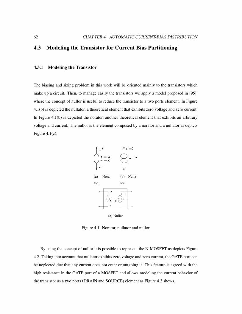
62 CHAPTER 4. AUTOMATIC CURRENT-BIAS DISTRIBUTION
4.3 Modeling the Transistor for Current Bias Partitioning
4.3.1 Modeling the Transistor
The biasing and sizing problem in this work will be oriented mainly to the transistors which
make up a circuit. Then, to manage easily the transistors we apply a model proposed in [95],
where the concept of nullor is useful to reduce the transistor to a two ports element. In Figure
4.1(b) is depicted the nullator, a theoretical element that exhibits zero voltage and zero current.
In Figure 4.1(b) is depicted the norator, another theoretical element that exhibits an arbitrary
voltage and current. The nullor is the element composed by a norator and a nullator as depicts
Figure 4.1(c).
(a) Nora-
tor.
(b) Nulla-
tor
(c) Nullor
Figure 4.1: Norator, nullator and nullor
By using the concept of nullor it is possible to represent the N-MOSFET as depicts Figure
4.2. Taking into account that nullator exhibits zero voltage and zero current, the GATE port can
be neglected due that any current does not enter or outgoing it. This feature is agreed with the
high resistance in the GATE port of a MOSFET and allows modeling the current behavior of
the transistor as a two ports (DRAIN and SOURCE) element as Figure 4.3 shows.
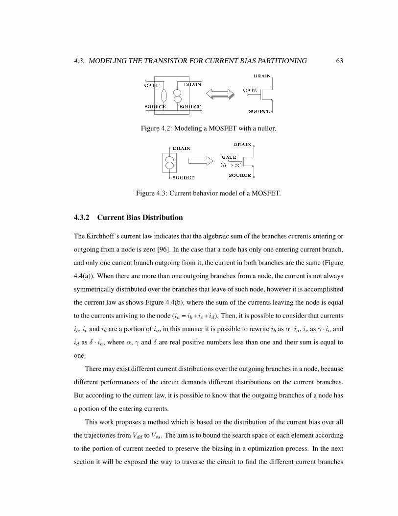
4.3. MODELING THE TRANSISTOR FOR CURRENT BIAS PARTITIONING 63
Figure 4.2: Modeling a MOSFET with a nullor.
Figure 4.3: Current behavior model of a MOSFET.
4.3.2 Current Bias Distribution
The Kirchhoff’s current law indicates that the algebraic sum of the branches currents entering or
outgoing from a node is zero [96]. In the case that a node has only one entering current branch,
and only one current branch outgoing from it, the current in both branches are the same (Figure
4.4(a)). When there are more than one outgoing branches from a node, the current is not always
symmetrically distributed over the branches that leave of such node, however it is accomplished
the current law as shows Figure 4.4(b), where the sum of the currents leaving the node is equal
to the currents arriving to the node (ia = ib+ic+id). Then, it is possible to consider that currents
ib, ic and id are a portion of ia, in this manner it is possible to rewrite ib as α ⋅ ia, ic as γ ⋅ ia and
id as δ ⋅ ia, where α, γ and δ are real positive numbers less than one and their sum is equal to
one.
There may exist different current distributions over the outgoing branches in a node, because
different performances of the circuit demands different distributions on the current branches.
But according to the current law, it is possible to know that the outgoing branches of a node has
a portion of the entering currents.
This work proposes a method which is based on the distribution of the current bias over all
the trajectories from Vdd to Vss. The aim is to bound the search space of each element according
to the portion of current needed to preserve the biasing in a optimization process. In the next
section it will be exposed the way to traverse the circuit to find the different current branches

64 CHAPTER 4. AUTOMATIC CURRENT-BIAS DISTRIBUTION
(a) One out-
going current
branch.
(b) Several outgoing current
branches
Figure 4.4: Examples of outgoing currents branches.
and how the current bias is distributed in each element.
4.4 Circuits and graphs
4.4.1 Incidence Matrix
From a given circuit it can be build a directed graphG = ⟨N,B⟩ where N is the set of nodes and
B the set of current branches. In order to build that graph, it is used the “Incidence Matrix” [97]
denoted by Ak×l where its rows represent the nodes N = n1, n2, . . . , nk (all nodes except
the reference node as Vss or ground) and its columns represent the branches (circuit elements)
B = b1, b2, . . . , bl. The values of each element aij in A are 0, 1 or -1 according to (4.1).
With the matrix A it is possible to build a directed graph that represents a circuit, in the
following way:
• The graph has k nodes and l branches.
• A 1 in the ith row and the jth column means that the branch j leaves the node i.
• A -1 in the ith row and the jth column means that the branch j enters to the node i.
• A 0 (or empty) in the ith row and the jth column means that the branch j does not enter
or leave the node i.
4.4. CIRCUITS AND GRAPHS 65
A =
b1 b2 . . . bl
n2
n2
⋮
nk
⎡⎢⎢⎢⎢⎢⎢⎢⎢⎢⎢⎢⎢⎣
a11
a21
⋮
ak1
a12
a22
⋮
ak2
. . .
. . .
⋱
. . .
a1l
a2l
⋮
akl
⎤⎥⎥⎥⎥⎥⎥⎥⎥⎥⎥⎥⎥⎦
where aij =
⎧⎪⎪⎪⎪⎪⎪⎪⎨⎪⎪⎪⎪⎪⎪⎪⎩
1 if bj leaves ni
−1 if bj arrives to ni
0 or empty otherwise
(4.1)
4.4.2 Depth First Search for biasing
Once the graph is described with the matrix A and the above issues, it is possible to explore the
graph to find all the current trajectories. Then it is used a “Depth First Search” (dfs algorithm)
[98] shown in Algorithm 9. There is a vector labeled as V isited flag which associates a flag
to each branch in order to know whether it has been already visited and avoid visiting it twice.
This recursive algorithm explores all the adjacent branches to a given branch. It is considered
the adjacent branches of a branch b, those branches which share the same node as b.
Algorithm 9 Depth First Search Algorithm (dfs)
Input: a branch b
1: visited flag[b]← visited
2: for each branch bi adjacent to b do
3: dfs(bi) if V isited flag[bi] ≠ visited
4: end for
The dfs algorithm is modified to find the different distributions (Levels) of the current bias
in each branch represented by an element (transistor) of the circuit. Then we proposed a top-
down algorithm dfsTD shown in Algorithm 10 which has as arguments: the current branch b,
the upper node of b namely n and the bias level CurLevel. As before, there exists a vector flag
called as V isited which associates a flag to each branch , but now, there is other more vector

66 CHAPTER 4. AUTOMATIC CURRENT-BIAS DISTRIBUTION
Algorithm 10 Depth First Search Algorithm Top-Down (dfsTD)
Input: b, n, CurLevel
1: V isited[b]← visited
2: Bn ← set of outgoing branches from n different of b
3: if Bn ≠ ∅ then
4: for each branch bi ∈ Bn do CurLevel− = 1
5: else
6: CurLevel ← level of the upper branch of b
7: end if
8: Bias Level[b]← CurLevel
9: n← lower node of b
10: for each entering branch to n do CurLevel+ = 1
11: Bn ← set of outgoing branches from n
12: for each branch bi ∈ Bn do
13: dfsTD(bi, n,CurLevel) if V isited[bi] ≠ visited
14: end for
called Bias level which associates the bias level to each branch. This algorithm traverses the
circuit in a top-down approach: from Vdd to Vss.
The first step in Algorithm 10 is to mark the branch b as visited one. The second line stores
in Bn the outgoing branches from n different of b. Next, line 3 evaluates whether Bn is different
from empty to subtract one to CurLevel for each branch bi in Bn. If Bn is an empty set, it
means that there are not adjacent branches to b, and therefore, the branch b has the same level
than its upper branch. In the line 8, the level (CurLevel) is assigned to the branch b . Line 9
sets to n the lower node of b. Afterwards, the line 10 finds the branches that enter to the new
node n and for each one of them, it is added one to CurLevel. In line 11, it is repeated the
procedure of line 2 (with the new node n), and finally in line 12, there is a recurrence of the
dfsTP to itself, if bi has not been visited. In this manner, it is possible to find the current level
in a given branch.
Process described in lines 2, 6, 9, 10 and 11, are performed by using the incidence matrix

4.5. PROPOSED CURRENT-BRANCHES-BIAS ASSIGNMENT (CBBA) APPROACH 67
(A), because that matrix contains all the information about the nodes, branches, their connec-
tions and directions.
4.5 Proposed Current-Branches-Bias Assignment (CBBA) Approach
Our proposed Current-Branches-Bias Assignment (CBBA) approach distributes the current bias
reference(s) according to the depth of each element (branch), and it can be summarized as
follows:
1. Replace all transistors by their nullor equivalent (see Figure 4.3).
2. Build the incidence matrix A of the equivalent circuit, i.e. (4.1).
3. Build (G = ⟨N,B⟩) from the incidence matrix A.
4. Apply recursively Algorithm 10 .
Algorithm 11 describes the above steps: from a SPICE circuit netlist, in line 1 matrix A is
generated as in (4.1). Next, from line 2 to line 5, the vector flag V isited is initialized to control
the recursive calls and the flag vector Bias level. The distributed or partitioned level is stored
as a result of the auto-biasing process. In line 6 the outgoing branches from Vdd, are stored in
BV dd. Next, for each branch bi in BV dd the CurLevel is initialized with zero, the method sets
the zero level to bi and labels it as a visited branch. In line 11, the lower node of bi is stored in
n, with the aim to build vector Bn formed by all the outgoing branches from node n in line 12.
In lines 13 to 15 there is a recursive call to dfsTD for each branch bj , if it has not been already
visited. At last, each branch has been assigned a level, where the lower level requires more part
of the space search (in other words, it holds more current than in the rest of levels).
When each branch has a current bias level, it is possible to perform a procedure to set the
limits of the search space for each variable. We propose an heuristic procedure to assign a
quantity proportional to the current bias level: let Xl be the lower and Xu the upper limits of
the whole search space, Lkl the low limit and Lku the upper limits in the search space for the k-th
level.

68 CHAPTER 4. AUTOMATIC CURRENT-BIAS DISTRIBUTION
Algorithm 11 Distribution of CurrentsInput: A circuit netlist, specifing Vdd and Vss node
1: Build the matrix A and the graph G = ⟨N,B⟩
2: for each branch bi ∈ B do
3: V isited[bi]← not visited
4: Bias level[bi]← 0
5: end for
6: BVdd ← set of branches outgoing from node Vdd
7: for each branch bi ∈ BVdd do
8: CurLevel ← 0
9: Bias level[bi]← 0
10: V isited[bi]← visited
11: n← the lower node of bi
12: Bn ← set of outgoing branches from n
13: for each branch bj ∈ Bn do
14: dfsTD(bj , n,CurLevel) if V isited[bj] ≠ visited
15: CurLevel = 0
16: end for
17: end for
Algorithm 12 describes the assignment procedure. It consists of dividing the search space
into sub-spaces according to the total number of levels (TL). The first step is devoted to divide
the entire search space into two parts, corresponding to the two first levels (level 0 and level
1). Those two parts share an intersection region to relax the partitioning and allow exploring
beyond the bound limits. The intersection between two levels (ν∩) depends on the total number
of levels and can be controlled by using an integer scaling factor (χ) as shown by (4.2). Since
TL > 0 and χ > 0, then ν∩ < 0.5. In our experiments, we used χ = 1.
ν∩ = (TL + χ)−1 (4.2)

4.5. PROPOSED CURRENT-BRANCHES-BIAS ASSIGNMENT (CBBA) APPROACH 69
Algorithm 12 Limit search space assignment procedureInput: Xl,Xu,TL
1: k = 0
2: Xu′ =Xu
3: ν∩ = (TL + χ)−1
4: while k < TL do
5: Xkl =Xu′ ∗ ν∩
6: Xku =Xu′
7: Xk+1l =Xl
8: Xu′ = Laux ∗ (1 − ν∩)
9: Xk+1u =Xu′
10: k+ = 2
11: end while
12: if TL is odd then
13: XTLl =Xl
14: XTLu =Xu′
15: end if
In this manner the first loop in Algorithm 12 (lines 5 to 10) generates a result like Figure
4.5(a). For the second loop the process is repeated but this time the upper limit is bounded by
Xu′ as shown in Figure 4.5(b). The algorithm continues until splitting the search space for all
the levels.
When the number of levels is odd, Algorithm 12 assigns to the last level Xl, its lower limit,
and the last value of Xu′ to its upper limit. In Figure 4.6 is depicted the result of Algorithm 12
for 5 levels (TL = 5).
All these CBBAs and bound limits in the search space can be used within an optimization
process by choosing different values for the sizing of each MOSFET. The main advantage is
preserving the DC operating point of the circuit.

70 CHAPTER 4. AUTOMATIC CURRENT-BIAS DISTRIBUTION
Level 1 Level 0
Xl Xu′ν∩ · Xu′ (1 − ν∩) · Xu′Search space
(a) First loop Algorithm 12
Level 1 Level 0
Level 2Level 3
Xl (1 − ν∩) · Xu′ XuSearch spaceν∩ · Xu′
(b) Second loop Algorithm 12
Figure 4.5: First two loops of Algorithm 12.
Level 1 Level 0
Level 2Level 3
Space Search
Level 4
Xl Xu
Figure 4.6: Limit search space assignment.
4.6 Application Examples
Our proposed CBBA approach is tested in optimizing two analog circuits: the Folded Cascode
(FC) Operational Transconductance Amplifier (OTA) shown in Figure 4.7, and the Recycled
Folded Cascode (RFC) OTA shown in Figure 4.8.
The FC OTA is encoded with seven variables (design parameters) for the MOSFETs,
x = [x1, . . . , x7]T as shown in the left side of Table 4.1, and the RFC OTA with ten vari-
ables, x = [x1, . . . , x10]T as shown in the right side of Table 4.1. Both circuits are biased
with Iref = 400µA and VDD = 1.8V . The measurements were executed with a load capac-
itor of 5.6pF and HSPICE® simulations were performed with a LEVEL 54 standard CMOS
Technology of 90 nm.
For the FC and RFC OTAs is used the circuit depicted on Figure 4.9 for yielding the volt-
ages: Vbn1, Vbn2, Vbp1 and Vbp2. In Table 4.2 are listed the sizes for each transistor of the
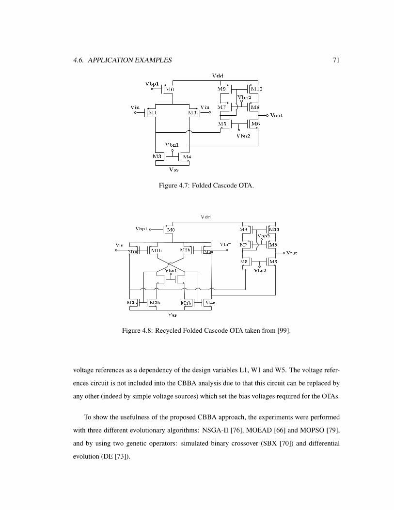
4.6. APPLICATION EXAMPLES 71
Figure 4.7: Folded Cascode OTA.
Figure 4.8: Recycled Folded Cascode OTA taken from [99].
voltage references as a dependency of the design variables L1, W1 and W5. The voltage refer-
ences circuit is not included into the CBBA analysis due to that this circuit can be replaced by
any other (indeed by simple voltage sources) which set the bias voltages required for the OTAs.
To show the usefulness of the proposed CBBA approach, the experiments were performed
with three different evolutionary algorithms: NSGA-II [76], MOEAD [66] and MOPSO [79],
and by using two genetic operators: simulated binary crossover (SBX [70]) and differential
evolution (DE [73]).
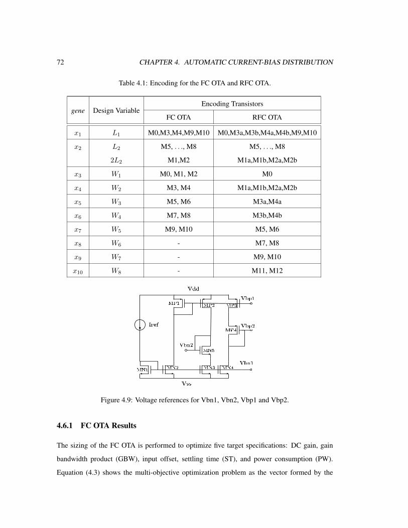
72 CHAPTER 4. AUTOMATIC CURRENT-BIAS DISTRIBUTION
Table 4.1: Encoding for the FC OTA and RFC OTA.
gene Design VariableEncoding Transistors
FC OTA RFC OTA
x1 L1 M0,M3,M4,M9,M10 M0,M3a,M3b,M4a,M4b,M9,M10
x2 L2 M5, . . ., M8 M5, . . ., M8
2L2 M1,M2 M1a,M1b,M2a,M2b
x3 W1 M0, M1, M2 M0
x4 W2 M3, M4 M1a,M1b,M2a,M2b
x5 W3 M5, M6 M3a,M4a
x6 W4 M7, M8 M3b,M4b
x7 W5 M9, M10 M5, M6
x8 W6 - M7, M8
x9 W7 - M9, M10
x10 W8 - M11, M12
Figure 4.9: Voltage references for Vbn1, Vbn2, Vbp1 and Vbp2.
4.6.1 FC OTA Results
The sizing of the FC OTA is performed to optimize five target specifications: DC gain, gain
bandwidth product (GBW), input offset, settling time (ST), and power consumption (PW).
Equation (4.3) shows the multi-objective optimization problem as the vector formed by the
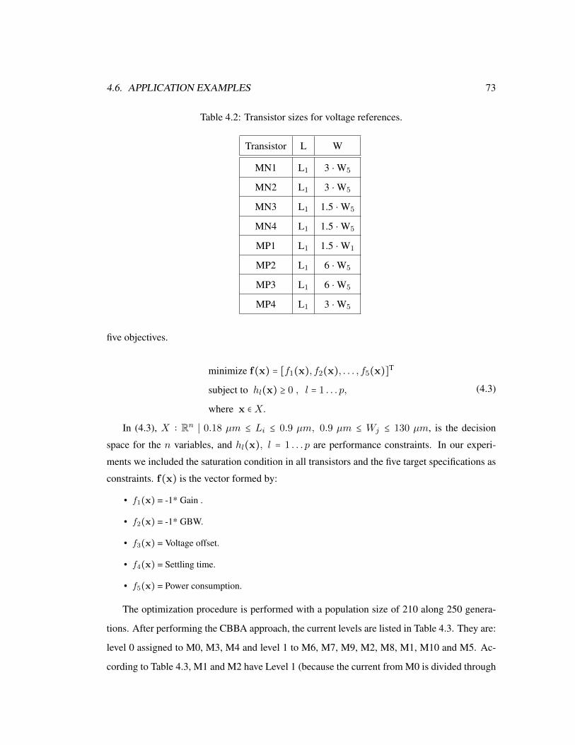
4.6. APPLICATION EXAMPLES 73
Table 4.2: Transistor sizes for voltage references.
Transistor L W
MN1 L1 3 ⋅ W5
MN2 L1 3 ⋅ W5
MN3 L1 1.5 ⋅ W5
MN4 L1 1.5 ⋅ W5
MP1 L1 1.5 ⋅ W1
MP2 L1 6 ⋅ W5
MP3 L1 6 ⋅ W5
MP4 L1 3 ⋅ W5
five objectives.
minimize f(x) = [f1(x), f2(x), . . . , f5(x)]T
subject to hl(x) ≥ 0 , l = 1 . . . p,
where x ∈X.
(4.3)
In (4.3), X ∶ Rn ∣ 0.18 µm ≤ Li ≤ 0.9 µm, 0.9 µm ≤ Wj ≤ 130 µm, is the decision
space for the n variables, and hl(x), l = 1 . . . p are performance constraints. In our experi-
ments we included the saturation condition in all transistors and the five target specifications as
constraints. f(x) is the vector formed by:
• f1(x) = -1* Gain .
• f2(x) = -1* GBW.
• f3(x) = Voltage offset.
• f4(x) = Settling time.
• f5(x) = Power consumption.
The optimization procedure is performed with a population size of 210 along 250 genera-
tions. After performing the CBBA approach, the current levels are listed in Table 4.3. They are:
level 0 assigned to M0, M3, M4 and level 1 to M6, M7, M9, M2, M8, M1, M10 and M5. Ac-
cording to Table 4.3, M1 and M2 have Level 1 (because the current from M0 is divided through
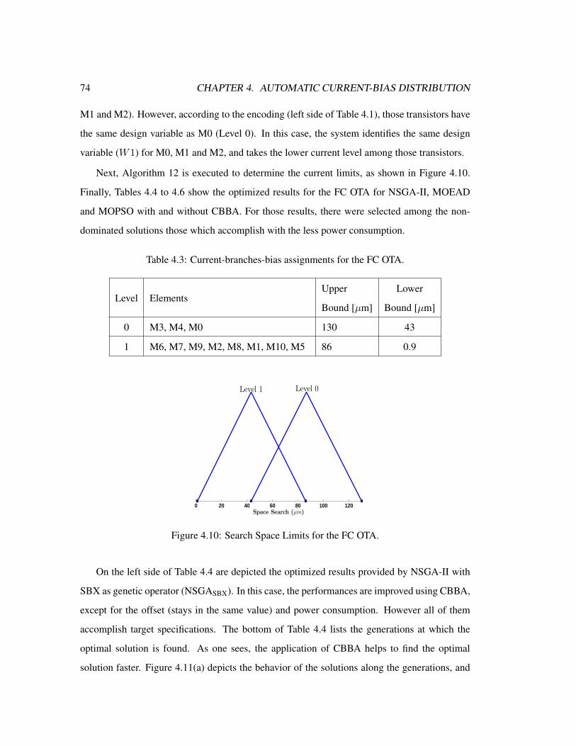
74 CHAPTER 4. AUTOMATIC CURRENT-BIAS DISTRIBUTION
M1 and M2). However, according to the encoding (left side of Table 4.1), those transistors have
the same design variable as M0 (Level 0). In this case, the system identifies the same design
variable (W1) for M0, M1 and M2, and takes the lower current level among those transistors.
Next, Algorithm 12 is executed to determine the current limits, as shown in Figure 4.10.
Finally, Tables 4.4 to 4.6 show the optimized results for the FC OTA for NSGA-II, MOEAD
and MOPSO with and without CBBA. For those results, there were selected among the non-
dominated solutions those which accomplish with the less power consumption.
Table 4.3: Current-branches-bias assignments for the FC OTA.
Level ElementsUpper Lower
Bound [µm] Bound [µm]
0 M3, M4, M0 130 43
1 M6, M7, M9, M2, M8, M1, M10, M5 86 0.9
0 20 40 60 80 100 120Space Search (µm)
Level 1 Level 0
Figure 4.10: Search Space Limits for the FC OTA.
On the left side of Table 4.4 are depicted the optimized results provided by NSGA-II with
SBX as genetic operator (NSGASBX). In this case, the performances are improved using CBBA,
except for the offset (stays in the same value) and power consumption. However all of them
accomplish target specifications. The bottom of Table 4.4 lists the generations at which the
optimal solution is found. As one sees, the application of CBBA helps to find the optimal
solution faster. Figure 4.11(a) depicts the behavior of the solutions along the generations, and

4.6. APPLICATION EXAMPLES 75
when CBBA is used, the number of biased solutions increase.
The optimal solutions for NSGADE are depicted on the right side of Table 4.4. The opti-
mal solutions without CBBA do not accomplish the power consumption specification, but the
use of CBBA overcomes that issue at generation 221. Regarding to the number of solutions,
Figure 4.11(b) depicts a slight increase, showing that CBBA allows accomplishing all target
specifications.
The results provided by MOEADSBX are listed on the left side of Table 4.5. Without CBBA,
the optimal solution exhibits a fail around 15% in the GBW value compared with the target
specification (70 MHz). When CBBA is used, the optimal solution accomplishes the GBW
and all the circuit performances are improved except for the power consumption that shows an
increment of 5% compared with the target specification. The number of biased solutions for
this experiment increased 4x when CBBA is used, as shown in Figure 4.12(a).
MOEADDE results (right side of Table 4.5) exhibits a similar behavior regarding to the ob-
jective values, but this time, the GBW fails almost 50% without CBBA. Using CBBA achieves
accomplishing the GBW specification, although the gain is 2% below the specification and the
power consumption is 10% higher than specification. Therefore, CBBA helps to find more
solutions and more close to the specifications, as shown in Figure 4.12(b).
Table 4.6 shows the objective values for the optimal solutions with MOPSO. This time,
CBBA preserves the circuit performances (except for settling time an power that exhibit a slight
increment), but the optimal solution is found around 30 generations faster. Figure 4.13 shows
that all the population achieves solutions almost 70 generations faster when CBBA is used.
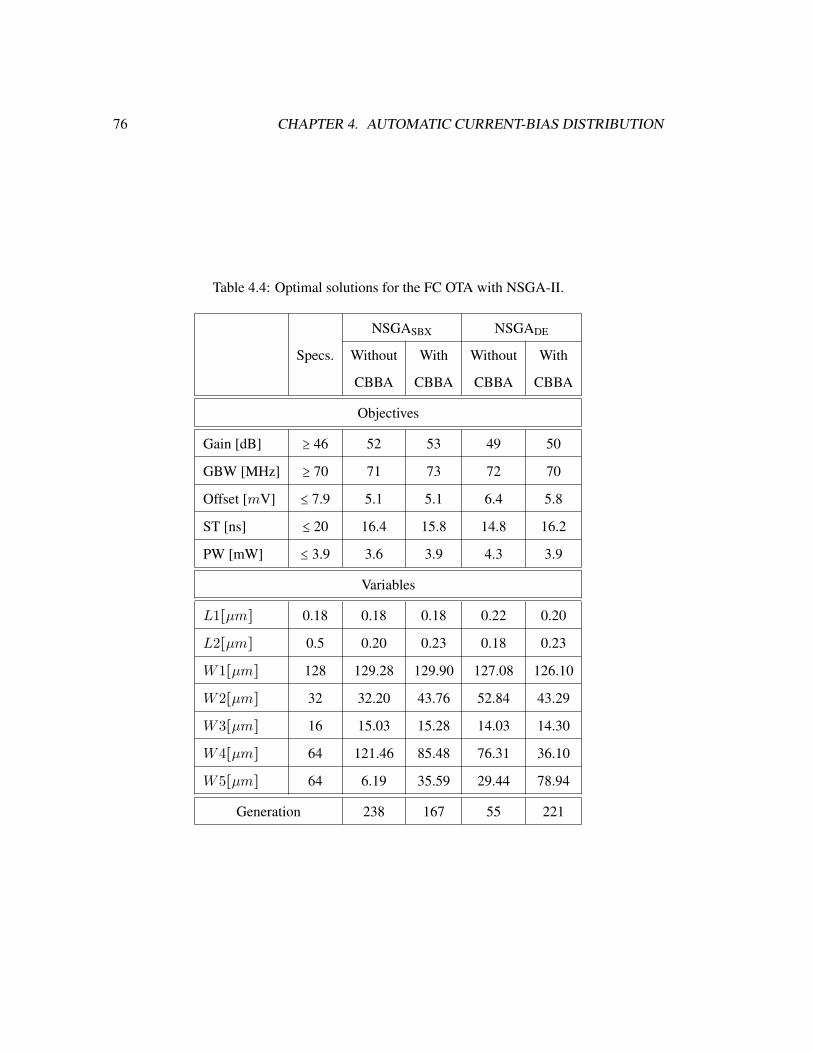
76 CHAPTER 4. AUTOMATIC CURRENT-BIAS DISTRIBUTION
Table 4.4: Optimal solutions for the FC OTA with NSGA-II.
Specs.
NSGASBX NSGADE
Without With Without With
CBBA CBBA CBBA CBBA
Objectives
Gain [dB] ≥ 46 52 53 49 50
GBW [MHz] ≥ 70 71 73 72 70
Offset [mV] ≤ 7.9 5.1 5.1 6.4 5.8
ST [ns] ≤ 20 16.4 15.8 14.8 16.2
PW [mW] ≤ 3.9 3.6 3.9 4.3 3.9
Variables
L1[µm] 0.18 0.18 0.18 0.22 0.20
L2[µm] 0.5 0.20 0.23 0.18 0.23
W1[µm] 128 129.28 129.90 127.08 126.10
W2[µm] 32 32.20 43.76 52.84 43.29
W3[µm] 16 15.03 15.28 14.03 14.30
W4[µm] 64 121.46 85.48 76.31 36.10
W5[µm] 64 6.19 35.59 29.44 78.94
Generation 238 167 55 221
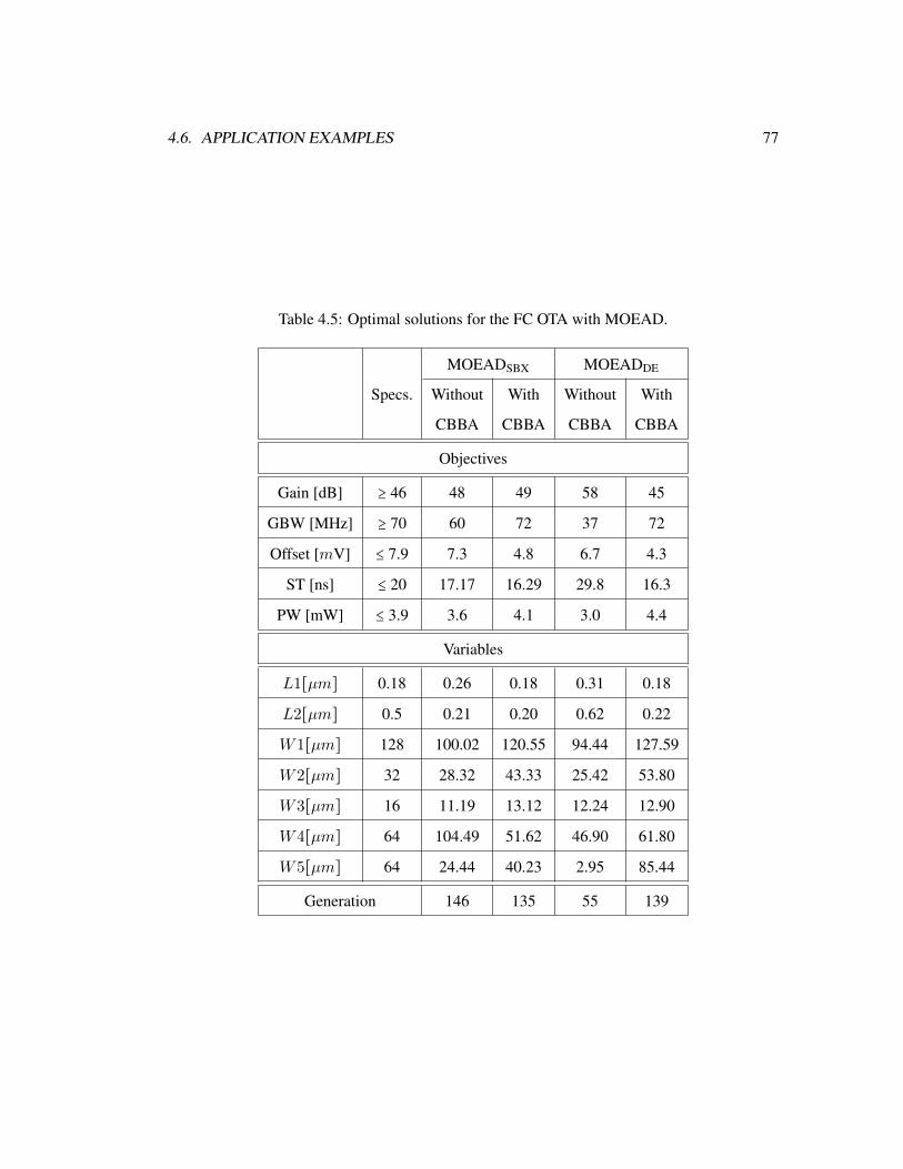
4.6. APPLICATION EXAMPLES 77
Table 4.5: Optimal solutions for the FC OTA with MOEAD.
Specs.
MOEADSBX MOEADDE
Without With Without With
CBBA CBBA CBBA CBBA
Objectives
Gain [dB] ≥ 46 48 49 58 45
GBW [MHz] ≥ 70 60 72 37 72
Offset [mV] ≤ 7.9 7.3 4.8 6.7 4.3
ST [ns] ≤ 20 17.17 16.29 29.8 16.3
PW [mW] ≤ 3.9 3.6 4.1 3.0 4.4
Variables
L1[µm] 0.18 0.26 0.18 0.31 0.18
L2[µm] 0.5 0.21 0.20 0.62 0.22
W1[µm] 128 100.02 120.55 94.44 127.59
W2[µm] 32 28.32 43.33 25.42 53.80
W3[µm] 16 11.19 13.12 12.24 12.90
W4[µm] 64 104.49 51.62 46.90 61.80
W5[µm] 64 24.44 40.23 2.95 85.44
Generation 146 135 55 139
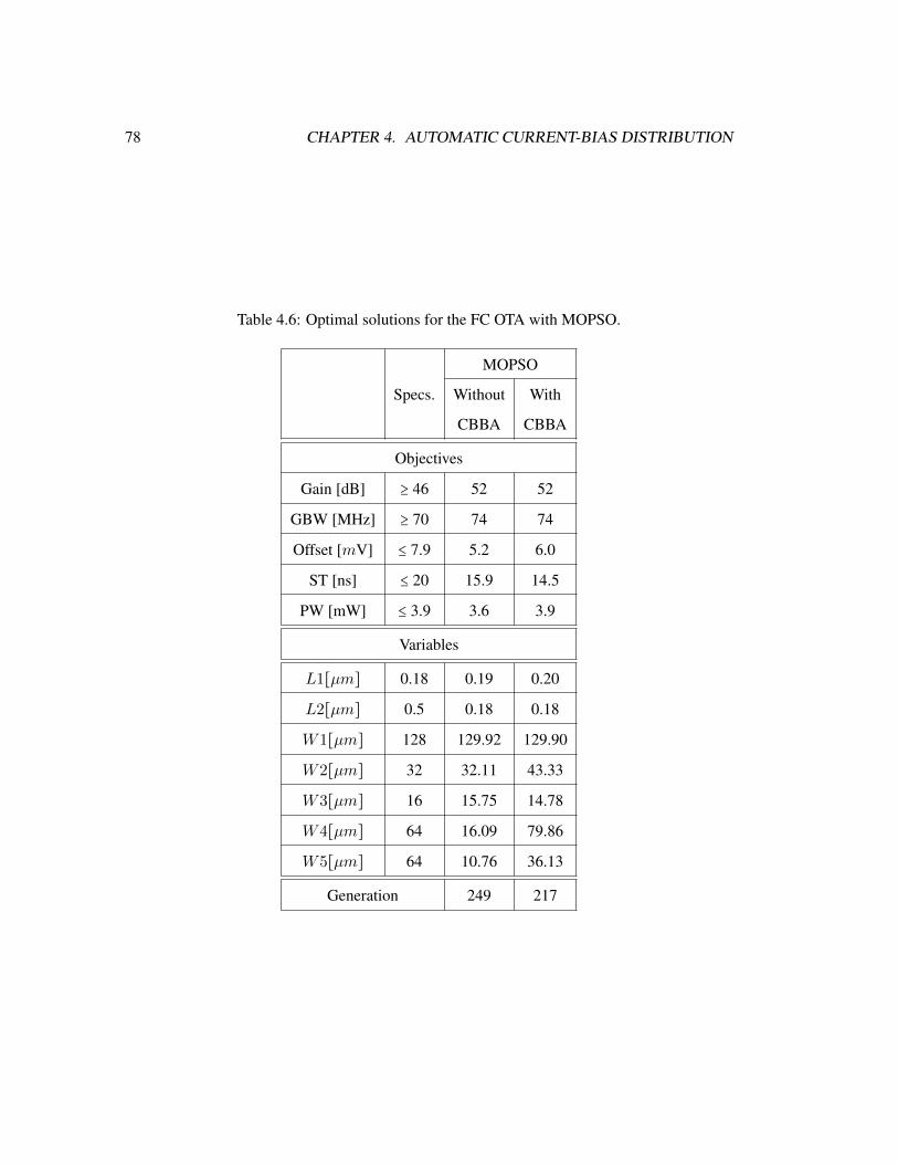
78 CHAPTER 4. AUTOMATIC CURRENT-BIAS DISTRIBUTION
Table 4.6: Optimal solutions for the FC OTA with MOPSO.
Specs.
MOPSO
Without With
CBBA CBBA
Objectives
Gain [dB] ≥ 46 52 52
GBW [MHz] ≥ 70 74 74
Offset [mV] ≤ 7.9 5.2 6.0
ST [ns] ≤ 20 15.9 14.5
PW [mW] ≤ 3.9 3.6 3.9
Variables
L1[µm] 0.18 0.19 0.20
L2[µm] 0.5 0.18 0.18
W1[µm] 128 129.92 129.90
W2[µm] 32 32.11 43.33
W3[µm] 16 15.75 14.78
W4[µm] 64 16.09 79.86
W5[µm] 64 10.76 36.13
Generation 249 217
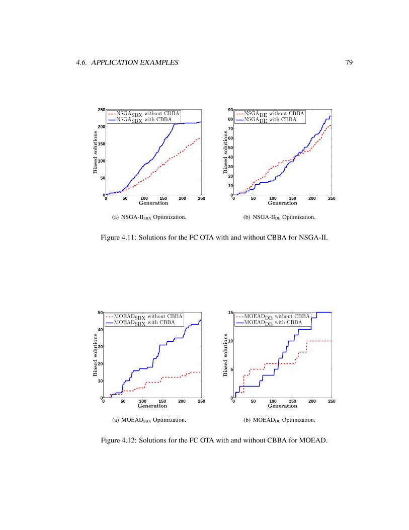
4.6. APPLICATION EXAMPLES 79
0 50 100 150 200 2500
50
100
150
200
250
Generation
Biased
solutions
NSGASBX without CBBANSGASBX with CBBA
(a) NSGA-IISBX Optimization.
0 50 100 150 200 2500
10
20
30
40
50
60
70
80
90
Generation
Biased
solutions
NSGADE without CBBANSGADE with CBBA
(b) NSGA-IIDE Optimization.
Figure 4.11: Solutions for the FC OTA with and without CBBA for NSGA-II.
0 50 100 150 200 2500
10
20
30
40
50
Generation
Biased
solutions
MOEADSBX without CBBAMOEADSBX with CBBA
(a) MOEADSBX Optimization.
0 50 100 150 200 2500
5
10
15
Generation
Biased
solutions
MOEADDE without CBBAMOEADDE with CBBA
(b) MOEADDE Optimization.
Figure 4.12: Solutions for the FC OTA with and without CBBA for MOEAD.
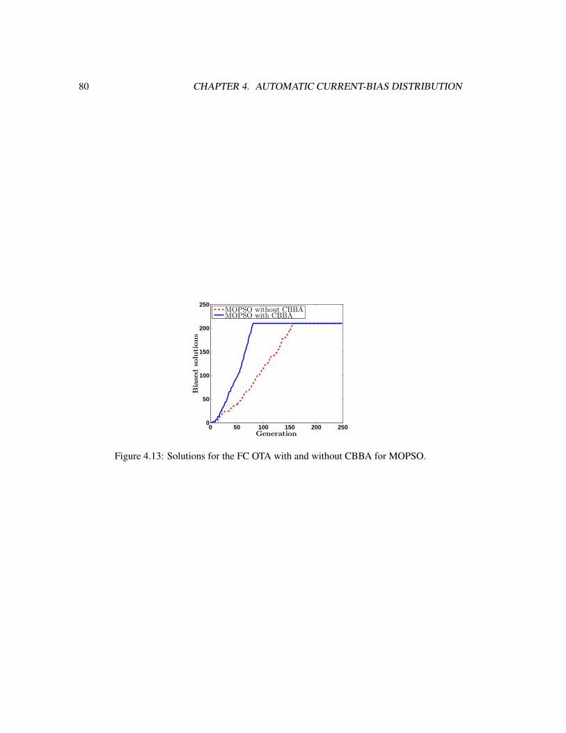
80 CHAPTER 4. AUTOMATIC CURRENT-BIAS DISTRIBUTION
0 50 100 150 200 2500
50
100
150
200
250
Generation
Biased
solutions
MOPSO without CBBAMOPSO with CBBA
Figure 4.13: Solutions for the FC OTA with and without CBBA for MOPSO.
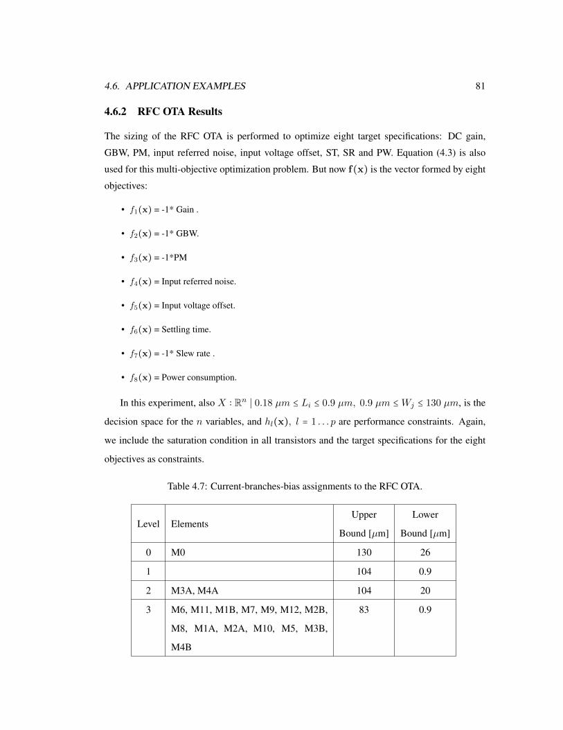
4.6. APPLICATION EXAMPLES 81
4.6.2 RFC OTA Results
The sizing of the RFC OTA is performed to optimize eight target specifications: DC gain,
GBW, PM, input referred noise, input voltage offset, ST, SR and PW. Equation (4.3) is also
used for this multi-objective optimization problem. But now f(x) is the vector formed by eight
objectives:
• f1(x) = -1* Gain .
• f2(x) = -1* GBW.
• f3(x) = -1*PM
• f4(x) = Input referred noise.
• f5(x) = Input voltage offset.
• f6(x) = Settling time.
• f7(x) = -1* Slew rate .
• f8(x) = Power consumption.
In this experiment, also X ∶ Rn ∣ 0.18 µm ≤ Li ≤ 0.9 µm, 0.9 µm ≤Wj ≤ 130 µm, is the
decision space for the n variables, and hl(x), l = 1 . . . p are performance constraints. Again,
we include the saturation condition in all transistors and the target specifications for the eight
objectives as constraints.
Table 4.7: Current-branches-bias assignments to the RFC OTA.
Level ElementsUpper Lower
Bound [µm] Bound [µm]
0 M0 130 26
1 104 0.9
2 M3A, M4A 104 20
3 M6, M11, M1B, M7, M9, M12, M2B,
M8, M1A, M2A, M10, M5, M3B,
M4B
83 0.9
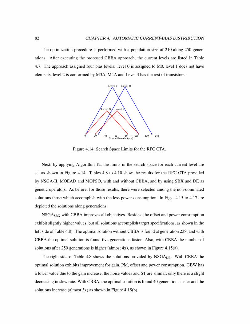
82 CHAPTER 4. AUTOMATIC CURRENT-BIAS DISTRIBUTION
The optimization procedure is performed with a population size of 210 along 250 gener-
ations. After executing the proposed CBBA approach, the current levels are listed in Table
4.7. The approach assigned four bias levels: level 0 is assigned to M0, level 1 does not have
elements, level 2 is conformed by M3A, M4A and Level 3 has the rest of transistors.
0 20 40 60 80 100 120 140
Level 0Level 1
Level 2Level 3
Space Search (µm)
Figure 4.14: Search Space Limits for the RFC OTA.
Next, by applying Algorithm 12, the limits in the search space for each current level are
set as shown in Figure 4.14. Tables 4.8 to 4.10 show the results for the RFC OTA provided
by NSGA-II, MOEAD and MOPSO, with and without CBBA, and by using SBX and DE as
genetic operators. As before, for those results, there were selected among the non-dominated
solutions those which accomplish with the less power consumption. In Figs. 4.15 to 4.17 are
depicted the solutions along generations.
NSGASBX with CBBA improves all objectives. Besides, the offset and power consumption
exhibit slightly higher values, but all solutions accomplish target specifications, as shown in the
left side of Table 4.8). The optimal solution without CBBA is found at generation 238, and with
CBBA the optimal solution is found five generations faster. Also, with CBBA the number of
solutions after 250 generations is higher (almost 4x), as shown in Figure 4.15(a).
The right side of Table 4.8 shows the solutions provided by NSGADE. With CBBA the
optimal solution exhibits improvement for gain, PM, offset and power consumption. GBW has
a lower value due to the gain increase, the noise values and ST are similar, only there is a slight
decreasing in slew rate. With CBBA, the optimal solution is found 40 generations faster and the
solutions increase (almost 3x) as shown in Figure 4.15(b).
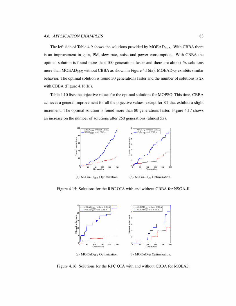
4.6. APPLICATION EXAMPLES 83
The left side of Table 4.9 shows the solutions provided by MOEADSBX. With CBBA there
is an improvement in gain, PM, slew rate, noise and power consumption. With CBBA the
optimal solution is found more than 100 generations faster and there are almost 5x solutions
more than MOEADSBX without CBBA as shown in Figure 4.16(a). MOEADDE exhibits similar
behavior. The optimal solution is found 30 generations faster and the number of solutions is 2x
with CBBA (Figure 4.16(b)).
Table 4.10 lists the objective values for the optimal solutions for MOPSO. This time, CBBA
achieves a general improvement for all the objective values, except for ST that exhibits a slight
increment. The optimal solution is found more than 80 generations faster. Figure 4.17 shows
an increase on the number of solutions after 250 generations (almost 5x).
0 50 100 150 200 2500
20
40
60
80
100
Generation
Biased
solutions
NSGASBX without CBBANSGASBX with CBBA
(a) NSGA-IISBX Optimization.
0 50 100 150 200 2500
5
10
15
20
25
30
35
Generation
Biased
solutions
NSGADE without CBBANSGADE with CBBA
(b) NSGA-IIDE Optimization.
Figure 4.15: Solutions for the RFC OTA with and without CBBA for NSGA-II.
0 50 100 150 200 2500
5
10
15
20
25
Generation
Biased
solutions
MOEADSBX without CBBAMOEADSBX with CBBA
(a) MOEADSBX Optimization.
0 50 100 150 200 2500
2
4
6
8
10
12
Generation
Biased
solutions
MOEADDE without CBBAMOEADDE with CBBA
(b) MOEADDE Optimization.
Figure 4.16: Solutions for the RFC OTA with and without CBBA for MOEAD.
84 CHAPTER 4. AUTOMATIC CURRENT-BIAS DISTRIBUTION
Table 4.8: Optimal solutions for the RFC OTA with NSGA-II.
Specs.
NSGASBX NSGADE
Without With Without With
CBBA CBBA CBBA CBBA
Objectives
Gain [dB] ≥ 55 65 61 61 64
GBW [MHz] ≥ 70 111 113 139 120
PM [deg] ≥ 65 62 68 65 75
Offset [mV] ≤ 11 0.15 0.30 0.51 0.28
ST [ns] ≤ 20 16.9 16.5 15.36 16
SR [V/µs] ≥ 48 80 120 97 87
Noise [µVrms] ≤ 69 70 69 68 68
PW [mW] ≤ 3.5 3.2 3.4 3.5 3.3
Variables
L1[µm] 0.18 0.23 0.18 0.18 0.21
L2[µm] 0.5 0.24 0.18 0.19 0.18
W1[µm] 64 129.98 129.00 87.19 75.66
W2[µm] 32 126.00 82.15 127.12 78.39
W3[µm] 12 98.66 100.46 53.02 20.8
W4[µm] 4 41.49 47.77 17.45 72.42
W5[µm] 8 14.05 13.64 10.17 9.34
W6[µm] 32 65.3 82.06 128.53 66.84
W7[µm] 32 6.42 6.04 65.56 15.60
W8[µm] 4 7.03 2.96 29.58 46.91
Generation 238 233 166 126
4.7 Summary
A new current-branches-bias assignment (CBBA) approach has been introduced in order to
accelerate the sizing process of an analog integrated circuit composed of MOSFETs. The ap-
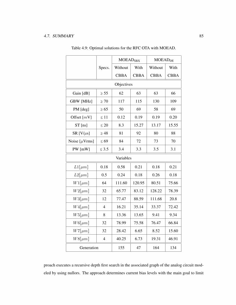
4.7. SUMMARY 85
Table 4.9: Optimal solutions for the RFC OTA with MOEAD.
Specs.
MOEADSBX MOEADDE
Without With Without With
CBBA CBBA CBBA CBBA
Objectives
Gain [dB] ≥ 55 62 63 63 66
GBW [MHz] ≥ 70 117 115 130 109
PM [deg] ≥ 65 50 69 58 69
Offset [mV] ≤ 11 0.12 0.19 0.19 0.20
ST [ns] ≤ 20 8.3 15.27 13.17 15.55
SR [V/µs] ≥ 48 81 92 80 88
Noise [µVrms] ≤ 69 84 72 73 70
PW [mW] ≤ 3.5 3.4 3.3 3.5 3.1
Variables
L1[µm] 0.18 0.58 0.21 0.18 0.21
L2[µm] 0.5 0.24 0.18 0.26 0.18
W1[µm] 64 111.60 120.95 80.51 75.66
W2[µm] 32 65.77 83.12 128.22 78.39
W3[µm] 12 77.47 88.59 111.68 20.8
W4[µm] 4 16.21 35.14 33.37 72.42
W5[µm] 8 13.36 13.65 9.41 9.34
W6[µm] 32 78.99 75.58 76.47 66.84
W7[µm] 32 28.42 6.65 8.52 15.60
W8[µm] 4 40.25 6.73 19.31 46.91
Generation 155 47 164 134
proach executes a recursive depth first search in the associated graph of the analog circuit mod-
eled by using nullors. The approach determines current bias levels with the main goal to limit
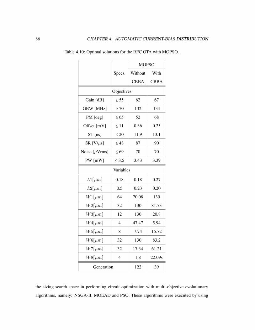
86 CHAPTER 4. AUTOMATIC CURRENT-BIAS DISTRIBUTION
Table 4.10: Optimal solutions for the RFC OTA with MOPSO.
Specs.
MOPSO
Without With
CBBA CBBA
Objectives
Gain [dB] ≥ 55 62 67
GBW [MHz] ≥ 70 132 134
PM [deg] ≥ 65 52 68
Offset [mV] ≤ 11 0.36 0.25
ST [ns] ≤ 20 11.9 13.1
SR [V/µs] ≥ 48 87 90
Noise [µVrms] ≤ 69 70 70
PW [mW] ≤ 3.5 3.43 3.39
Variables
L1[µm] 0.18 0.18 0.27
L2[µm] 0.5 0.23 0.20
W1[µm] 64 70.08 130
W2[µm] 32 130 81.73
W3[µm] 12 130 20.8
W4[µm] 4 47.47 5.94
W5[µm] 8 7.74 15.72
W6[µm] 32 130 83.2
W7[µm] 32 17.34 61.21
W8[µm] 4 1.8 22.09s
Generation 122 39
the sizing search space in performing circuit optimization with multi-objective evolutionary
algorithms, namely: NSGA-II, MOEAD and PSO. These algorithms were executed by using
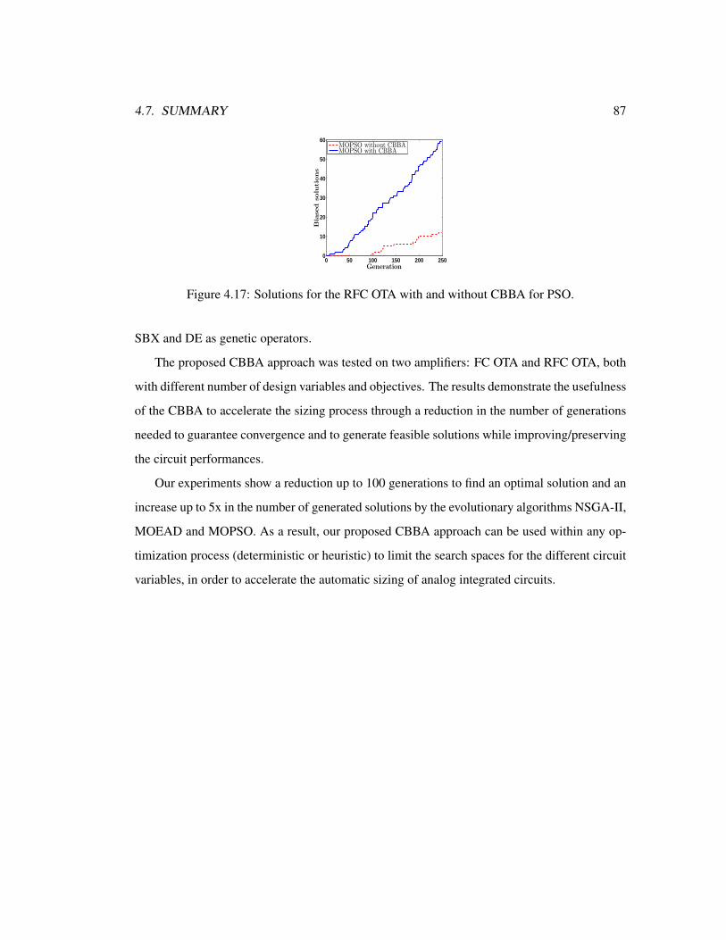
4.7. SUMMARY 87
0 50 100 150 200 2500
10
20
30
40
50
60
Generation
Biased
solutions
MOPSO without CBBAMOPSO with CBBA
Figure 4.17: Solutions for the RFC OTA with and without CBBA for PSO.
SBX and DE as genetic operators.
The proposed CBBA approach was tested on two amplifiers: FC OTA and RFC OTA, both
with different number of design variables and objectives. The results demonstrate the usefulness
of the CBBA to accelerate the sizing process through a reduction in the number of generations
needed to guarantee convergence and to generate feasible solutions while improving/preserving
the circuit performances.
Our experiments show a reduction up to 100 generations to find an optimal solution and an
increase up to 5x in the number of generated solutions by the evolutionary algorithms NSGA-II,
MOEAD and MOPSO. As a result, our proposed CBBA approach can be used within any op-
timization process (deterministic or heuristic) to limit the search spaces for the different circuit
variables, in order to accelerate the automatic sizing of analog integrated circuits.

88 CHAPTER 4. AUTOMATIC CURRENT-BIAS DISTRIBUTION
Chapter 5
Circuit Variation Analysis
5.1 Introduction
This chapter is devoted to describe the variation analysis for analog circuits. It is exposed an
outline of support variation methodologies and their classifications. It is presented a worst case
approach by including sensitivity in the optimization of analog circuits by using the Richardson
extrapolation. Finally, it is performed a non-worst case yield optimization by using an allocation
budget simulations with the aim to reduce the runtime.
5.2 Variation Analysis for Analog Circuits
The analog design optimization involves not only finding nominal solutions to accomplish de-
sired performances with constraints, but also it requires that such solutions guarantee robustness
in front to the fabrication process [51, 100]. For instance, let xi = (xi1, xi2) be a design that de-
scribes a given circuit in the variables search space. xi is subject to process variations and the
design variables can lie into a “Tolerance Region” (Rtol), defined by the nominal values and the
tolerances for each one of the design values. The process variation is depicted in Fig. 5.1 where
each point represents a different design of the same circuit and Ritol is the tolerance region for
xi.
Then Rtol is the set of all the tolerance regions of the different designs. It is possible
89
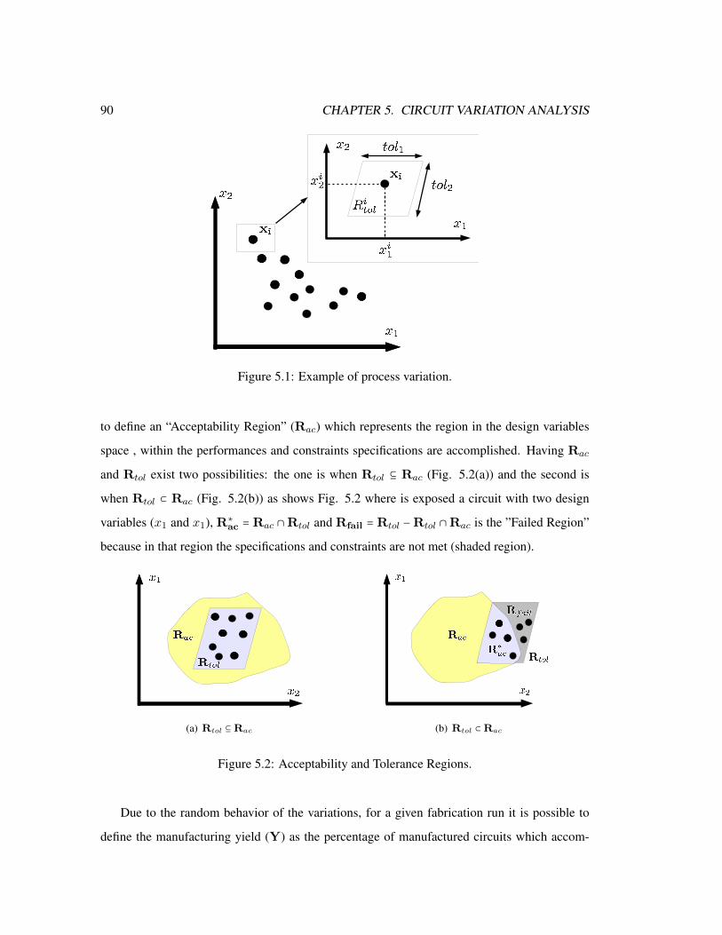
90 CHAPTER 5. CIRCUIT VARIATION ANALYSIS
Figure 5.1: Example of process variation.
to define an “Acceptability Region” (Rac) which represents the region in the design variables
space , within the performances and constraints specifications are accomplished. Having Rac
and Rtol exist two possibilities: the one is when Rtol ⊆ Rac (Fig. 5.2(a)) and the second is
when Rtol ⊂ Rac (Fig. 5.2(b)) as shows Fig. 5.2 where is exposed a circuit with two design
variables (x1 and x1), R∗ac = Rac ∩Rtol and Rfail = Rtol −Rtol ∩Rac is the ”Failed Region”
because in that region the specifications and constraints are not met (shaded region).
(a) Rtol ⊆Rac (b) Rtol ⊂Rac
Figure 5.2: Acceptability and Tolerance Regions.
Due to the random behavior of the variations, for a given fabrication run it is possible to
define the manufacturing yield (Y) as the percentage of manufactured circuits which accom-
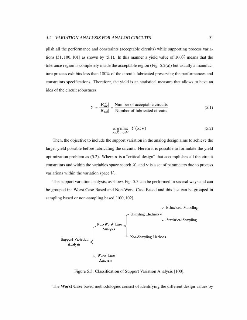
5.2. VARIATION ANALYSIS FOR ANALOG CIRCUITS 91
plish all the performance and constraints (acceptable circuits) while supporting process varia-
tions [51, 100, 101] as shown by (5.1). In this manner a yield value of 100% means that the
tolerance region is completely inside the acceptable region (Fig. 5.2(a)) but usually a manufac-
ture process exhibits less than 100% of the circuits fabricated preserving the performances and
constraints specifications. Therefore, the yield is an statistical measure that allows to have an
idea of the circuit robustness.
Y = ∣R∗ac∣
∣Rtol∣= Number of acceptable circuits
Number of fabricated circuits(5.1)
arg maxx∈X , v∈V
Y (x,v) (5.2)
Then, the objective to include the support variation in the analog design aims to achieve the
larger yield possible before fabricating the circuits. Herein it is possible to formulate the yield
optimization problem as (5.2). Where x is a “critical design” that accomplishes all the circuit
constraints and within the variables space search X , and v is a set of parameters due to process
variations within the variation space V .
The support variation analysis, as shows Fig. 5.3 can be performed in several ways and can
be grouped in: Worst Case Based and Non-Worst Case Based and this last can be grouped in
sampling based or non-sampling based [100, 102].
Figure 5.3: Classification of Support Variation Analysis [100].
The Worst Case based methodologies consist of identifying the different design values by

92 CHAPTER 5. CIRCUIT VARIATION ANALYSIS
exploring the search space that produces extreme performances. This task can be performed
with a vertex analysis as in WiCkeD [50] or as describes [100].
There exists a recent work in [103] where is performed a worst case bound analysis of
analog circuits by including variations. In this case, linear models for active devices and the
small signal transistor model are used to find transfer functions with variational coefficients for
including global and local variations. There are provided two examples: a low-pass filter and
an cascode op-amp, and this approach achieves an average speed up of 90x compared with a
classical Monte Carlo approach.
The Non-Worst Case based methodologies are grouped in Sampling and Non-Sampling
methods. Regarding to Non-Sampling methods it is possible to find works as in [102, 104] that
are based on the sensitivities of the circuit performances relative to each design variable. In this
case there are some issues to overcome to achieve that kind of analysis, as defining perturbation
factors for each design variable and the sensitivity calculation of a circuit when there is not
explicit equations that describe the performance as function of the design variables. Also this
approach may be stalled when it is desired to find more accurate results, due to that with two
slightly different design values the simulator finds the same performances result.
The sampling methods are grouped in: behavioral models based and statistical sampling
based. The behavioral model based methodologies build regression models through successive
simulations to estimate the yield, as in [105] where response surface methods are used and
in [5] that exploits the Kriging model to approximate the yield. All these methodologies build
the behavioral model by sampling and the number of samples needed is determined by the
desired level of accuracy, while more accuracy more samples are needed. Also, the complexity
of the models exhibit a strong dependence on the accuracy.
Finally, the statistical sampling based analysis, consist of calculating the yield from a large
number of samples generated randomly over the search space of the design variables by sim-
ulating the fabrication process [100]. To perform the yield analysis, the circuit performances
of each sample are calculated, and the number of samples that accomplish all the specifica-
tions and constraints divided by the total number of samples represents the yield. Once the
factory provides the statistical transistor model, the only shortcoming is choosing the number
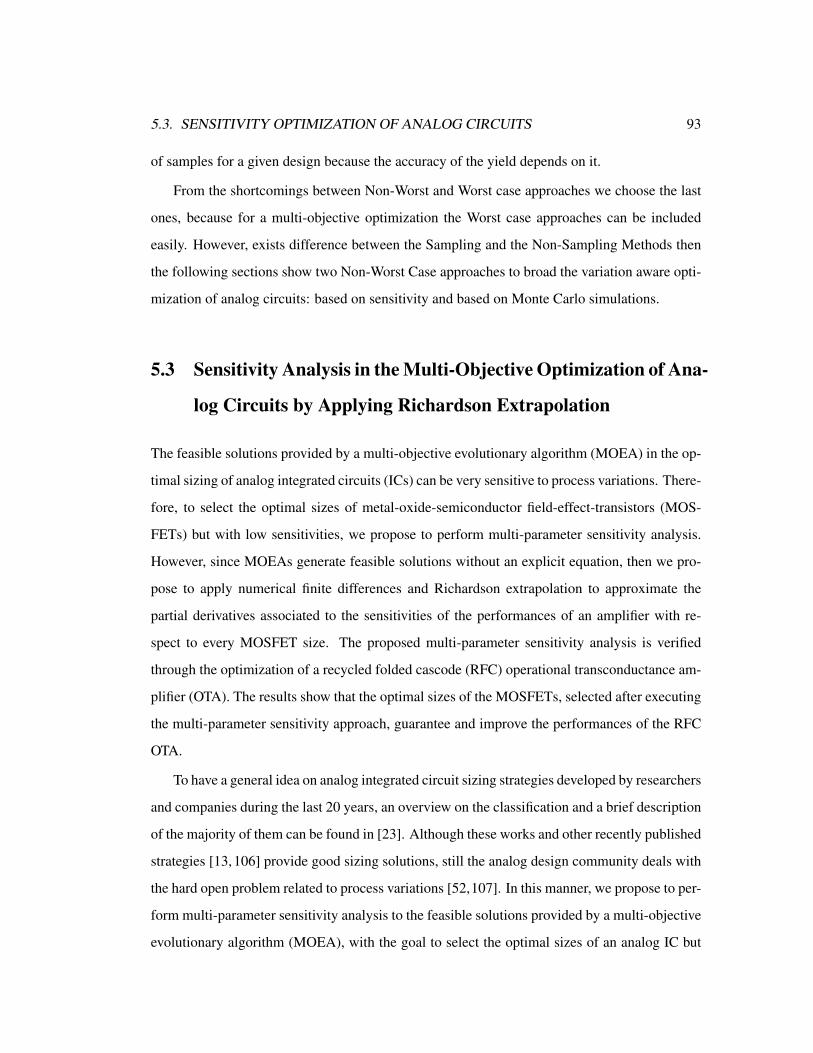
5.3. SENSITIVITY OPTIMIZATION OF ANALOG CIRCUITS 93
of samples for a given design because the accuracy of the yield depends on it.
From the shortcomings between Non-Worst and Worst case approaches we choose the last
ones, because for a multi-objective optimization the Worst case approaches can be included
easily. However, exists difference between the Sampling and the Non-Sampling Methods then
the following sections show two Non-Worst Case approaches to broad the variation aware opti-
mization of analog circuits: based on sensitivity and based on Monte Carlo simulations.
5.3 Sensitivity Analysis in the Multi-Objective Optimization of Ana-
log Circuits by Applying Richardson Extrapolation
The feasible solutions provided by a multi-objective evolutionary algorithm (MOEA) in the op-
timal sizing of analog integrated circuits (ICs) can be very sensitive to process variations. There-
fore, to select the optimal sizes of metal-oxide-semiconductor field-effect-transistors (MOS-
FETs) but with low sensitivities, we propose to perform multi-parameter sensitivity analysis.
However, since MOEAs generate feasible solutions without an explicit equation, then we pro-
pose to apply numerical finite differences and Richardson extrapolation to approximate the
partial derivatives associated to the sensitivities of the performances of an amplifier with re-
spect to every MOSFET size. The proposed multi-parameter sensitivity analysis is verified
through the optimization of a recycled folded cascode (RFC) operational transconductance am-
plifier (OTA). The results show that the optimal sizes of the MOSFETs, selected after executing
the multi-parameter sensitivity approach, guarantee and improve the performances of the RFC
OTA.
To have a general idea on analog integrated circuit sizing strategies developed by researchers
and companies during the last 20 years, an overview on the classification and a brief description
of the majority of them can be found in [23]. Although these works and other recently published
strategies [13,106] provide good sizing solutions, still the analog design community deals with
the hard open problem related to process variations [52,107]. In this manner, we propose to per-
form multi-parameter sensitivity analysis to the feasible solutions provided by a multi-objective
evolutionary algorithm (MOEA), with the goal to select the optimal sizes of an analog IC but
94 CHAPTER 5. CIRCUIT VARIATION ANALYSIS
with low sensitives. Because very often, the best feasible solutions meeting extreme perfor-
mance requirements are located at some peripherals of the feasible solution space, but some
variability in the design parameters can transform a best solution to a worst one [52, 107–109].
Since our proposed multi-parameter sensitivity analysis is performed from numerical data in-
stead of using explicit equations, we propose to apply numerical finite differences and Richard-
son extrapolation [110–113], to approximate the partial derivatives associated to the sensitivities
of the sizing relationships W/L (width/large) of the MOSFETs. These process are performed in
two domains: variables W/L (design parameters) and objectives, where both are evaluated by
linking HSPICE®.
The first step of our proposed approach consists on conventional optimization by applying the
MOEA called non-dominated sorting genetic algorithm (NSGA-II) [76]. The second step is
devoted to perform multi-parameter sensitivity analysis for all feasible solutions to discriminate
those located in a delicate point which does not support the natural variations of the fabrication
processes.
5.3.1 Multi-Parameter Sensitivity Analysis
The relative or normalized sensitivity (S) can be defined as the cause and effect relationship
between the circuit elements variations, and the resulting changes in the performances response
[114, 115]. Furthermore, in the design of analog ICs the lowest sensitivity is very desired.
Let fi(x) be an objective function (performance response), where x = [x1, . . . , xn]T are
the design variables. It is possible to relate small changes in the response of the performance
(∂fi , i ∈ [1,m]) to variations in the design variables (∂xj , j ∈ [1, n]). It leads us to the single
parameter sensitivity definition given by,
Sfixj ≃xj
fi
∂fi∂xj
. (5.3)
According to (5.3), there is one sensitivity for every objective function in f (see Eq.( 5.11))
and for every variable in x. Then, it is possible to define the multi-parameter sensitivity which
sums the different single sensitivities regarding the different variables for every objective as
5.3. SENSITIVITY OPTIMIZATION OF ANALOG CIRCUITS 95
follows [115]:
Sfj =¿ÁÁÀ
n
∑i=1
∣Sfjxi ∣2 ⋅ σ2xi , (5.4)
where Sfjxi is calculated by (5.3), σxi is a variability parameter of xi and the square root is used
to preserve the same units.
The performances of an analog IC are evaluated using HSPICE®, and they are considered
as the objective functions. As one can infer, using a numerical circuit simulator, there is not
possibility to derive an explicit equation for every performance or objective function. There-
fore, in order to calculate the partial derivative required by (5.3), the Richardson extrapolation
described by (5.5), is used herein.
∂fi∂xj
≈ gi(x, j, d) − gi(x, j,−d)2d
, with d→ 0 (5.5)
where function gi is defined as:
gi ∶Rn → R
gi(x, j, d) = fi(y) ∣yk = xk for k ≠ j and yj = xj + d(5.6)
In (5.5), d is a step parameter that is updated in each iteration [116], for this case
d = 2−udu−1, d0 is assigned to an initial value and u is the current iteration. The recursive
calculation continues until a tolerance error, as stopping criterion (δ), is reached.
Our proposed multi-parameter sensitivity analysis approach is based on the Richardson ex-
trapolation sketched in Algorithm 13. This algorithm is performed until the stopping criterion or
a maximum number of iterations, is reached. The Richardson extrapolation is a sequence accel-
eration method used to improve the rate of convergence of calculation of the partial derivatives.
Due to the iterative processes, it is possible to have stagnation in the f ′u,v evaluation (line 9
of Algorithm 13), when the very small value of d does not produce difference between f ′u,v−1
and f ′u−1,v−1. If that happens, the algorithm save the last value before the stagnation to avoid a
wrong derivative value.
For instance, let x = [x1, x2, x3]T be any solution from the feasible solutions set and
f(x) = [f1(x), f2(x), f3(x)]T its objective vector. For the objective function f1, and for a

96 CHAPTER 5. CIRCUIT VARIATION ANALYSIS
Algorithm 13 Richardson Extrapolation
1: h = h0
2: for u = 0;u < MaxLoops ;u++ do
3: for v = 0; v < MaxLoops ; v++ do
4: if v == 0 then
5: g+= Function evaluation with the parameter + d
6: g−= Function evaluation with the parameter - d
7: f ′u,v = (g+ − g−)/(2 ∗ d)
8: else
9: f ′u,v = f ′u,v−1 + (f ′u,v−1 − f ′u−1,v−1)/(2 ∗ ∗(2 ∗ v) − 1)
10: if ∣f ′u,v − f ′u,v−1∣ < δ then
11: break
12: end if
13: end if
14: d← d/2;
15: end for
16: end for
17: return f ′u,v
given initial value of d, the first estimations for the partial derivatives
∂f1
∂x1≈ g1(x,1, d) − g1(x,1,−d)
2d
∂f1
∂x2≈ g1(x,2, d) − g1(x,2,−d)
2d
∂f1
∂x3≈ g1(x,3, d) − g1(x,3,−d)
2d
are calculated. Next, the Richardson extrapolation is executed. That way, the multi-parameter
sensitivity for function f1 is calculated as
Sf1 =√
(Sf1x1)2σ2x1 + (Sf1x2)
2σ2x2 + (Sf1x3)
2σ2x3
The other multi-parameter sensitivities Sf2 and Sf3 are calculated with the same procedure.
In our implementation of the Richardson extrapolation, the three partial derivatives for all the
5.3. SENSITIVITY OPTIMIZATION OF ANALOG CIRCUITS 97
functions f1, f2 and f3, with respect to a variable xi (say x1), are calculated in a single HSPICE
simulation, because those values correspond to the variation of x1±d. The Richardson extrapo-
lation is executed until the stop criteria or the given maximum number the iterations is reached
for all the three partial derivatives.
With the aim to highlight the behavior of the Richardson extrapolation, an example on
the calculation of the multi-parameter sensitivity of the SRN function described by (5.7) [76],
is exposed herein. It consists to evaluate two objective functions [f1(x), f2(x)]T , with two
variables x = [x1, x2]T , and taking into account two constraints h1 and h2. This optimization
problem is minimized by using the NSGA-II algorithm, leading to the result shown in Figure
5.4. From these numerical feasible solutions we apply the Richardson extrapolation to evaluate
the sensitivity of every solution, with d0 = 5% for the current variable and δ < 1%.
0 50 100 150 200 250−250
−200
−150
−100
−50
0
50
f1
f 2
Figure 5.4: Optimization of SRN by applying NSGA-II.
SRN =
⎧⎪⎪⎪⎪⎪⎪⎪⎪⎪⎪⎨⎪⎪⎪⎪⎪⎪⎪⎪⎪⎪⎩
f1(x) = (x1 − 2)2 + (x2 − 1)2 + 2
f2(x) = 9x1 − (x2 − 1)2
h1(x) = x21 + x2
2 ≤ 225
h2(x) = x21 − 3x2
2 ≤ −10
(5.7)
Figure 5.5 shows the analytical and numerical solution by applying Richardson extrapo-
lation of the partial derivatives for f1 and f2 for the variable x1: ∂f1/∂x1 = 2(x1 − 2) and
∂f2/∂x1 = 9. These results demonstrate that the Richardson extrapolation calculated numeri-
98 CHAPTER 5. CIRCUIT VARIATION ANALYSIS
0 50 100 150 200
−0.2
0
0.2
0.4
0.6
0.8
1
f1
Sf1
x1
−6 −4 −2 0 2−14
−12
−10
−8
−6
−4
−2
x1
df1/dx1
RichardsonAnalytical
−4 −2 0−0.2
0
0.2
0.4
0.6
0.8
1
x1
Sf1
x1
−200 −150 −100 −50 0−1.5
−1
−0.5
0
0.5
1
1.5
f2
Sf2
x1
−6 −4 −2 0 29
9
9
9
9
9
x1
df2/dx1
RichardsonAnalytical
−4 −3 −2 −1 0−1.5
−1
−0.5
0
0.5
1
1.5
x1
Sf2
x1
Figure 5.5: Sensitivity of SRN with respect to x1.
cally, agrees with the result by evaluating (5.7) analytically.
If we focus on the sensitivity analysis, Figure 5.5 shows that for f1 the closer to zero values
of x1 exhibit low sensitivity, and for f2 the closer to zero values exhibit the lowest sensitivity
too. Figure 5.6 depicts the multi-parameter sensitivity evaluated from (5.4), for f1 and f2 with
σ = 1% (as variables represent sizes in circuit optimization, we consider the same variability
value for them); now it can be noted that few values of both functions exhibit low sensitivity.
0 50 100 150 200 2500.005
0.01
0.015
0.02
0.025
f1
Sf 1
−250 −200 −150 −100 −50 0 500
0.1
0.2
0.3
0.4
f2
Sf 2
Figure 5.6: Multi-parameter sensitivity of SRN function for f1 and f2.
Finally, from the feasible solution set it is possible to chose the multi-parameter sensitivity
lower than 0.015, considering both objective functions. As a result, the feasible solutions with
5.3. SENSITIVITY OPTIMIZATION OF ANALOG CIRCUITS 99
low sensitivities are shown in Figure 5.7. They were selected from the feasible solutions in Fig-
ure 5.4. This example demonstrates the usefulness of the Richardson extrapolation to perform
multi-parameter sensitivity analysis from numerical data.
0 20 40 60 80 100 120 140−120
−100
−80
−60
−40
−20
0
f1
f 2
Figure 5.7: Feasible solutions for SRN after applying multi-parameter sensitivity analysis.
5.3.2 Proposed Optimization System Including Multi-Parameter Sensitivity Anal-
ysis
Our proposed approach to select optimal sizes with low sensitivities has been programmed using
MATLAB®, and the circuit under optimization is simulated with HSPICE® through successive
simulations [72]. The optimization of the circuit performances is done by modifying the width
(W) and length (L) of the MOSFETs.
In Figure 5.8, it can be appreciated that our proposed optimization approach is divided into
two general stages: initialization and optimization. In the initialization stage the parameters
as maximum number of generations, population size and sensitivity parameters (d0 and δ), are
declared. In the second stage, the NSGA-II algorithm is applied to generate feasible solution
sets. In this stage HSPICE® is linked to evaluate the objective functions and constraints. Only
the solutions that meet the specifications (constraints) are introduced to the multi-parameter
sensitivity analysis based on the Richardson extrapolation. Afterwards, the non-dominated sort
is performed giving priority to the solutions with a measure of multi-parameter sensitivity be-
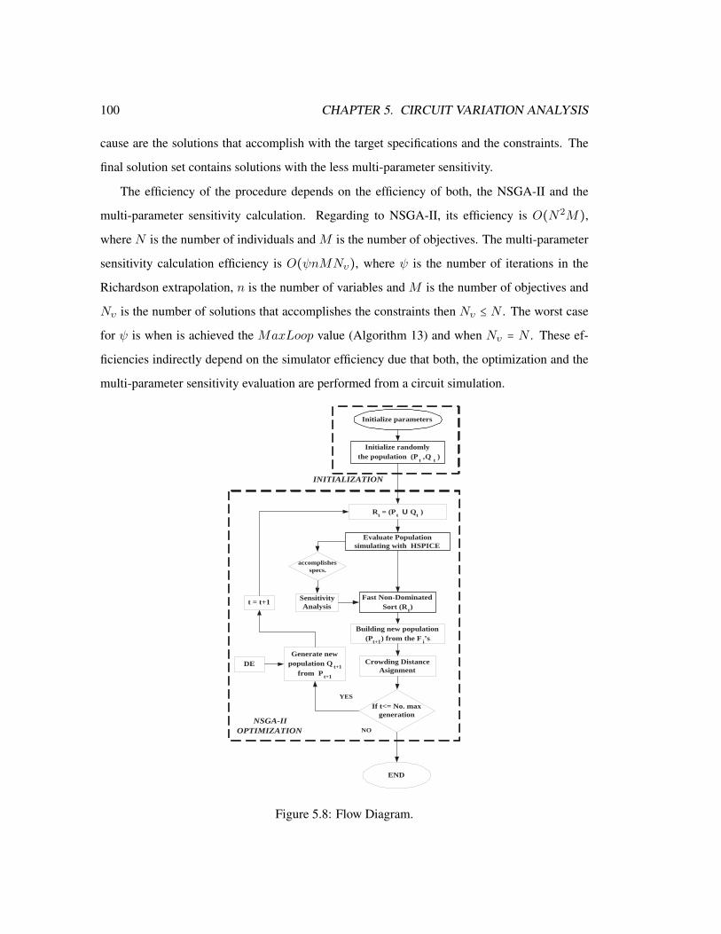
100 CHAPTER 5. CIRCUIT VARIATION ANALYSIS
cause are the solutions that accomplish with the target specifications and the constraints. The
final solution set contains solutions with the less multi-parameter sensitivity.
The efficiency of the procedure depends on the efficiency of both, the NSGA-II and the
multi-parameter sensitivity calculation. Regarding to NSGA-II, its efficiency is O(N2M),
where N is the number of individuals and M is the number of objectives. The multi-parameter
sensitivity calculation efficiency is O(ψnMNυ), where ψ is the number of iterations in the
Richardson extrapolation, n is the number of variables and M is the number of objectives and
Nυ is the number of solutions that accomplishes the constraints then Nυ ≤ N . The worst case
for ψ is when is achieved the MaxLoop value (Algorithm 13) and when Nυ = N . These ef-
ficiencies indirectly depend on the simulator efficiency due that both, the optimization and the
multi-parameter sensitivity evaluation are performed from a circuit simulation.
Initialize parameters
Initialize randomly the population (P
t , Q
t )
Evaluate Population simulating with HSPICE
Fast Non-Dominated Sort (R t )
If t<= No. max generation
END
NO
YES
Crowding Distance Asignment
R t = (P t U Q t )
Generate new population Q t+1
from P t+1
Building new population (P t+1 ) from the F i ’s
INITIALIZATION
NSGA-II OPTIMIZATION
DE
t = t+1 Sensitivity Analysis
accomplishes specs.
Figure 5.8: Flow Diagram.
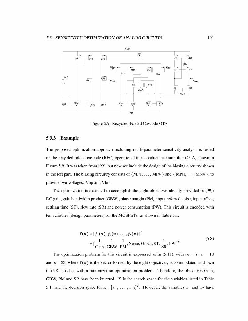
5.3. SENSITIVITY OPTIMIZATION OF ANALOG CIRCUITS 101
Iref
MP1
MN2 MN1
MP2
MN3 MN4
MP3
MP4
M1a M2a
M0
M3a M4a
M9 M10
M7 M8
M6
Vin- Vin+
Vbn2
Vbp2
M1b
M11 M12
Vbn2
M4b M3b
M2b
M5
Vout Vbn2 Vbp2
VDD
GND
Figure 5.9: Recycled Folded Cascode OTA.
5.3.3 Example
The proposed optimization approach including multi-parameter sensitivity analysis is tested
on the recycled folded cascode (RFC) operational transconductance amplifier (OTA) shown in
Figure 5.9. It was taken from [99], but now we include the design of the biasing circuitry shown
in the left part. The biasing circuitry consists of MP1, . . . , MP4 and MN1, . . . , MN4 , to
provide two voltages: Vbp and Vbn.
The optimization is executed to accomplish the eight objectives already provided in [99]:
DC gain, gain bandwidth product (GBW), phase margin (PM), input referred noise, input offset,
settling time (ST), slew rate (SR) and power consumption (PW). This circuit is encoded with
ten variables (design parameters) for the MOSFETs, as shown in Table 5.1.
f(x) = [f1(x), f2(x), . . . , f8(x)]T
= [ 1
Gain,
1
GBW,
1
PM,Noise,Offset,ST,
1
SR,PW]T
(5.8)
The optimization problem for this circuit is expressed as in (5.11), with m = 8, n = 10
and p = 33, where f(x) is the vector formed by the eight objectives, accommodated as shown
in (5.8), to deal with a minimization optimization problem. Therefore, the objectives Gain,
GBW, PM and SR have been inverted. X is the search space for the variables listed in Table
5.1, and the decision space for x = [x1, . . . , x10]T . However, the variables x1 and x2 have
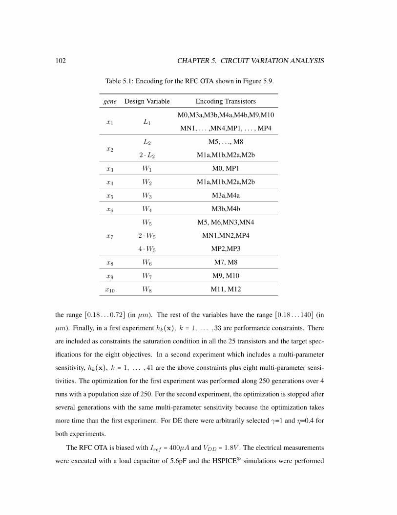
102 CHAPTER 5. CIRCUIT VARIATION ANALYSIS
Table 5.1: Encoding for the RFC OTA shown in Figure 5.9.
gene Design Variable Encoding Transistors
x1 L1
M0,M3a,M3b,M4a,M4b,M9,M10
MN1, . . . ,MN4,MP1, . . . , MP4
x2
L2 M5, . . ., M8
2 ⋅L2 M1a,M1b,M2a,M2b
x3 W1 M0, MP1
x4 W2 M1a,M1b,M2a,M2b
x5 W3 M3a,M4a
x6 W4 M3b,M4b
x7
W5 M5, M6,MN3,MN4
2 ⋅W5 MN1,MN2,MP4
4 ⋅W5 MP2,MP3
x8 W6 M7, M8
x9 W7 M9, M10
x10 W8 M11, M12
the range [0.18 . . .0.72] (in µm). The rest of the variables have the range [0.18 . . .140] (in
µm). Finally, in a first experiment hk(x), k = 1, . . . ,33 are performance constraints. There
are included as constraints the saturation condition in all the 25 transistors and the target spec-
ifications for the eight objectives. In a second experiment which includes a multi-parameter
sensitivity, hk(x), k = 1, . . . ,41 are the above constraints plus eight multi-parameter sensi-
tivities. The optimization for the first experiment was performed along 250 generations over 4
runs with a population size of 250. For the second experiment, the optimization is stopped after
several generations with the same multi-parameter sensitivity because the optimization takes
more time than the first experiment. For DE there were arbitrarily selected γ=1 and η=0.4 for
both experiments.
The RFC OTA is biased with Iref = 400µA and VDD = 1.8V . The electrical measurements
were executed with a load capacitor of 5.6pF and the HSPICE® simulations were performed
5.3. SENSITIVITY OPTIMIZATION OF ANALOG CIRCUITS 103
with a LEVEL 49 standard CMOS Technology of 0.18 µm. The parameters for the sensitivity
analysis are d0 = 3% for the design values, and δ = 3%. The aim to use percentage values for
d0 and δ, is the possibility to manage different design values with different magnitudes. In this
example, σi is proposed to be 3%.
The size of the final solution set is around 60, in average for all the runs in this experiment.
Table 5.2 shows the target specifications (Specs.), minimum, maximum, average and standard
deviation for all the objective functions among the final solution set, however those results do
not take into account the sensitivities of every feasible solution. The target specifications to
be improved are the values of the objective functions or performances evaluated with the sizes
already published in [99]. The application of our optimization stage provides better perfor-
mances compared to [99], for every objective function. These results are highlighted with bold
font. From Table 5.2 one can gain an insight on what to expect for this RFC OTA circuit topol-
ogy working under these design conditions. Later on, this table is an important base line to
compare the results that the multi-parameter sensitivity analysis will generate.
The optimization works with a multi-objective problem, then the best performances for the
eight objective functions are listed in Table 5.3, where x1 is the best solution for gain, x2 is
the best solution for GBW and so on with PM, Noise, Offset, ST, SR and PW. For instance,
the maximum gain (solution x1) is 68 dB; this best point, has GBW=107.97 MHz, PM=76.86
deg, Noise=52.62 µVrms, Offset=20.04 µV, ST= 17.10 nsecs, SR= 88.04 V/µsec and PW=
3.25 mWatts. This optimum gain is achieved with L1=0.36 µm, L2=0.18 µm, W1=132.48 µm,
W2=58.5 µm, W3=18.9 µm, W4=9.9 µm, W5=16.2 µm, W6=32.76 µm, W7=5.22 µm and
W8=24.3 µm.
The next step consisted of performing an optimization including a multi-parameter sensi-
tivity analysis. In such way that the sensitivity adds eight constraints more: the multi-parameter
sensitivities for each one of the eight objectives. Then we have in total 49 constraints for this
second experiment, the firsts 33 constraints accomplish with the specifications and the next
eight accomplish with the less multi-parameter sensitivity.
In this experiment the size of the final solution set is around the population size, although
that within such set, all the solutions accomplish the target specifications, each one has a differ-
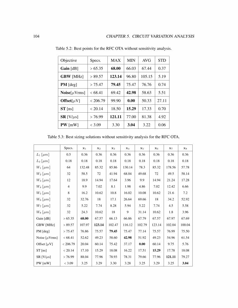
104 CHAPTER 5. CIRCUIT VARIATION ANALYSIS
Table 5.2: Best points for the RFC OTA without sensitivity analysis.
Objective Specs. MAX MIN AVG STD
Gain [dB] > 65.35 68.00 66.03 67.44 0.37
GBW [MHz] > 89.57 123.14 96.80 105.15 5.19
PM [deg] > 75.47 79.45 75.47 76.76 0.74
Noise[µVrms] < 68.41 69.42 42.98 58.63 5.51
Offset[µV] < 206.79 99.90 0.00 50.33 27.11
ST [ns] < 20.14 18.50 15.29 17.33 0.70
SR [V/µs] > 76.99 121.11 77.00 81.38 4.92
PW [mW] < 3.09 3.30 3.04 3.22 0.06
Table 5.3: Best sizing solutions without sensitivity analysis for the RFC OTA.
Specs. x1 x2 x3 x4 x5 x6 x7 x8
L1 [µm] 0.5 0.36 0.36 0.36 0.36 0.36 0.36 0.36 0.36
L2 [µm] 0.18 0.18 0.18 0.18 0.18 0.18 0.18 0.18 0.18
W1 [µm] 64 132.48 85.32 85.86 130.14 78.3 85.32 178.56 57.78
W2 [µm] 32 58.5 72 41.94 68.04 49.68 72 49.5 58.14
W3 [µm] 12 18.9 14.94 17.64 3.96 9.9 14.94 21.24 17.28
W4 [µm] 4 9.9 7.02 8.1 1.98 4.86 7.02 12.42 6.66
W5 [µm] 8 16.2 10.62 10.8 16.02 10.08 10.62 21.6 7.2
W6 [µm] 32 32.76 18 17.1 26.64 69.66 18 34.2 52.92
W7 [µm] 32 5.22 7.74 8.28 5.94 5.22 7.74 4.5 5.58
W8 [µm] 32 24.3 10.62 18 9 31.14 10.62 1.8 3.96
Gain [dB] > 65.35 68.00 67.57 66.13 66.86 67.79 67.57 67.97 67.69
GBW [MHz] > 89.57 107.97 123.14 102.47 116.12 102.79 123.14 102.04 100.04
PM [deg] > 75.47 76.86 75.57 79.45 75.47 77.14 75.57 76.99 75.50
Noise [µVrms] < 68.41 52.62 49.23 58.60 42.98 51.92 49.23 54.96 61.54
Offset [µV] < 206.79 20.04 60.14 75.42 37.17 0.00 60.14 9.75 5.76
ST [ns] < 20.14 17.10 15.29 18.08 16.22 17.51 15.29 17.78 18.08
SR [V/µs] > 76.99 88.04 77.96 78.93 78.31 79.66 77.96 121.11 79.27
PW [mW] < 3.09 3.25 3.29 3.30 3.28 3.25 3.29 3.25 3.04
5.3. SENSITIVITY OPTIMIZATION OF ANALOG CIRCUITS 105
ent value of multi-parameter sensitivity, then it is possible to chose the solutions with the lowest
one. By selecting the lowest five solutions in each run, the Table 5.4 shows the target spec-
ifications (Specs.), minimum, maximum, average and standard deviation for all the objective
functions including multi-parameter sensitivity in the optimization for every feasible solution.
As before, the target specifications to be improved are the values of the objective functions or
performances evaluated with the sizes already published in [99]. In this second experiment, it
is proposed selecting the feasible solutions with the lowest multi-parameter sensitivity, in this
case it is necessary to sacrifice some of the objectives with the aim to preserve the best values of
the remaining ones. Then it was decided to allow slightly higher values of power consumption.
The application of our optimization stage provides better performances compared to [99],
for every objective function except for power consumption which is slightly above the target
specification. As before, the best results are highlighted with bold font. By comparing Tables
5.2 and 5.4, it is possible to see how the best results from the first experiment were lost, but
nevertheless the best results for the second experiment still improve the targets except for the
power consumption. Gain, PM and PW are almost in the same value than the first experiment.
GBW, Noise and ST are closer to the first experiment values and finally, SR and Offset were
decreased significantly compared with the first experiment, but still they are better than targets
specs.
The best performances for the eight objective functions in the second experiment are listed
in Table 5.5, where x1 is the best solution for gain, x2 is the best solution for GBW and so on
with PM, Noise, Offset, ST, SR and PW. In this case, the solution for gain, GBW, PM, Noise,
ST and PW is the same (x1 = x2 = x3 = x4 = x6 = x8).
At the beginning of the optimization including multi-parameter sensitivity, there are taking
into account only the constraints that corresponding to the saturation condition of transistors and
targets specifications. As soon as a solution accomplishes those constraints, there are included
the multi-parameter sensitivity constraints, allowing categorize those solutions with the less
multi-parameter sensitivity among the best ones, to guide the optimization. During this process,
it is possible to see how the multi-parameter sensitivity is reduced from the moment when are
found solutions which accomplish the first constraints. When the multi-parameter sensitivity
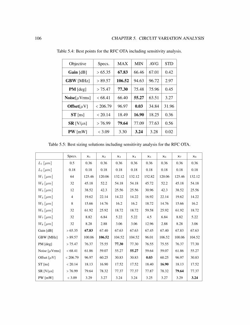
106 CHAPTER 5. CIRCUIT VARIATION ANALYSIS
Table 5.4: Best points for the RFC OTA including sensitivity analysis.
Objective Specs. MAX MIN AVG STD
Gain [dB] > 65.35 67.83 66.46 67.01 0.42
GBW [MHz] > 89.57 106.52 94.63 96.72 2.97
PM [deg] > 75.47 77.30 75.48 75.96 0.45
Noise[µVrms] < 68.41 66.40 55.27 63.51 3.27
Offset[µV] < 206.79 96.97 0.03 34.84 31.96
ST [ns] < 20.14 18.49 16.90 18.25 0.36
SR [V/µs] > 76.99 79.64 77.09 77.63 0.56
PW [mW] < 3.09 3.30 3.24 3.28 0.02
Table 5.5: Best sizing solutions including sensitivity analysis for the RFC OTA.
Specs. x1 x2 x3 x4 x5 x6 x7 x8
L1 [µm] 0.5 0.36 0.36 0.36 0.36 0.36 0.36 0.36 0.36
L2 [µm] 0.18 0.18 0.18 0.18 0.18 0.18 0.18 0.18 0.18
W1 [µm] 64 125.46 120.06 132.12 132.12 152.82 120.06 125.46 132.12
W2 [µm] 32 45.18 52.2 54.18 54.18 45.72 52.2 45.18 54.18
W3 [µm] 12 38.52 42.3 25.56 25.56 30.96 42.3 38.52 25.56
W4 [µm] 4 19.62 22.14 14.22 14.22 16.92 22.14 19.62 14.22
W5 [µm] 8 15.66 14.76 16.2 16.2 18.72 14.76 15.66 16.2
W6 [µm] 32 61.92 25.92 18.72 18.72 59.58 25.92 61.92 18.72
W7 [µm] 32 8.82 6.84 5.22 5.22 4.5 6.84 8.82 5.22
W8 [µm] 32 8.28 2.88 3.06 3.06 12.96 2.88 8.28 3.06
Gain [dB] > 65.35 67.83 67.40 67.63 67.63 67.45 67.40 67.83 67.63
GBW [MHz] > 89.57 100.06 106.52 104.52 104.52 96.01 106.52 100.06 104.52
PM [deg] > 75.47 76.37 75.55 77.30 77.30 76.55 75.55 76.37 77.30
Noise [µVrms] < 68.41 61.86 59.07 55.27 55.27 59.64 59.07 61.86 55.27
Offset [µV] < 206.79 96.97 60.25 30.83 30.83 0.03 60.25 96.97 30.83
ST [ns] < 20.14 18.13 16.90 17.52 17.52 18.40 16.90 18.13 17.52
SR [V/µs] > 76.99 79.64 78.32 77.37 77.37 77.87 78.32 79.64 77.37
PW [mW] < 3.09 3.29 3.27 3.24 3.24 3.25 3.27 3.29 3.24
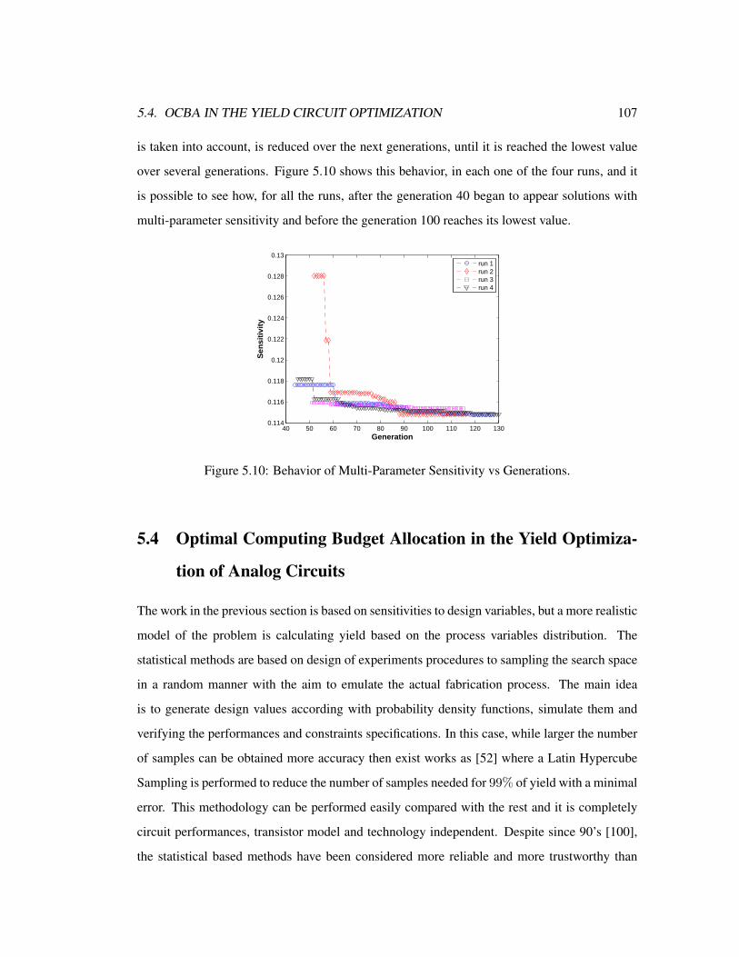
5.4. OCBA IN THE YIELD CIRCUIT OPTIMIZATION 107
is taken into account, is reduced over the next generations, until it is reached the lowest value
over several generations. Figure 5.10 shows this behavior, in each one of the four runs, and it
is possible to see how, for all the runs, after the generation 40 began to appear solutions with
multi-parameter sensitivity and before the generation 100 reaches its lowest value.
40 50 60 70 80 90 100 110 120 1300.114
0.116
0.118
0.12
0.122
0.124
0.126
0.128
0.13S
ensi
tivi
ty
Generation
run 1run 2run 3run 4
Figure 5.10: Behavior of Multi-Parameter Sensitivity vs Generations.
5.4 Optimal Computing Budget Allocation in the Yield Optimiza-
tion of Analog Circuits
The work in the previous section is based on sensitivities to design variables, but a more realistic
model of the problem is calculating yield based on the process variables distribution. The
statistical methods are based on design of experiments procedures to sampling the search space
in a random manner with the aim to emulate the actual fabrication process. The main idea
is to generate design values according with probability density functions, simulate them and
verifying the performances and constraints specifications. In this case, while larger the number
of samples can be obtained more accuracy then exist works as [52] where a Latin Hypercube
Sampling is performed to reduce the number of samples needed for 99% of yield with a minimal
error. This methodology can be performed easily compared with the rest and it is completely
circuit performances, transistor model and technology independent. Despite since 90’s [100],
the statistical based methods have been considered more reliable and more trustworthy than

108 CHAPTER 5. CIRCUIT VARIATION ANALYSIS
other methodologies, the computational effort to perform the statistical methodologies is high
due to the fact that each design needs to be simulated several times including the different
variations.
In this manner, we applied a budget allocation methodology on the yield multi-objective
optimization of analog circuits with the aim to reduce the time required for a classical yield
optimization based on statistical simulations.
5.4.1 Optimal Computing Budget Allocation (OCBA)
The main task in the analysis variation is to identify the best designs when the variables of
the circuit (x) are under variations (v). By setting a budget simulations there exist several
ways to distribute the simulations among the different designs. An Optimal Computing Budget
Allocation (OCBA) [117] is a strategy that distributes the large portion of the budget simulations
among the critical designs and limits the simulations for the non-critical designs with the aim
to enhance the efficiency of the optimization in simulation experiments. The final result of
applying an OCBA is a reduction in the total simulation cost.
Among the OCBAs there exists one in [118] (CCY) that achieves a 74% reduction in the
computation time. CCY has shown a reduction time of one order compared with the basic
Monte Carlo for mono-optimization yield [52]. By setting ψT as the total budget simulations
for the whole optimization and there are Nυ critical designs. Equation (5.2) now is defined as
(5.9), where ψi is the number of simulations performed for the i-th design.
arg maxx∈X , v∈V
Y (x,v) (5.9)
subject to ψT =Nυ
∑i
ψi
CCY proposes that from a total budget of simulations ψT to be distributed among Nυ de-
signs the yield problem can be maximized when (5.10) is accomplished, where b denotes the de-
sign having the best yield, σi is the variance of the i-th critical solution and
δb,i = Yb(x,v) − Yi(x,v) is the difference between the b-th and i-th yields. Such equations
maximize the probability that design b is actually the best design among Nυ designs [118].
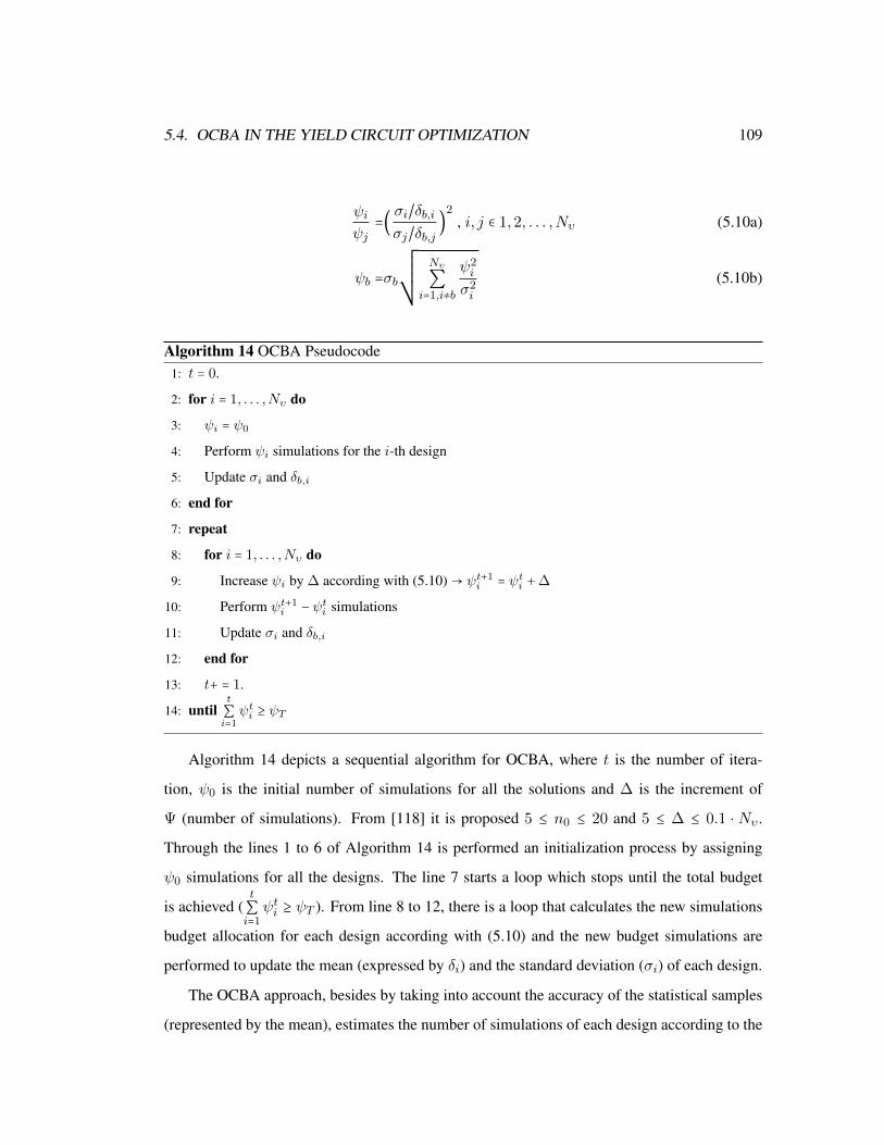
5.4. OCBA IN THE YIELD CIRCUIT OPTIMIZATION 109
ψiψj
=( σi/δb,iσj/δb,j
)2
, i, j ∈ 1,2, . . . ,Nυ (5.10a)
ψb =σb
¿ÁÁÁÀ
Nυ
∑i=1,i≠b
ψ2i
σ2i
(5.10b)
Algorithm 14 OCBA Pseudocode1: t = 0.
2: for i = 1, . . . ,Nυ do
3: ψi = ψ0
4: Perform ψi simulations for the i-th design
5: Update σi and δb,i
6: end for
7: repeat
8: for i = 1, . . . ,Nυ do
9: Increase ψi by ∆ according with (5.10) → ψt+1i = ψti +∆
10: Perform ψt+1i − ψti simulations
11: Update σi and δb,i
12: end for
13: t+ = 1.
14: untilt
∑i=1ψti ≥ ψT
Algorithm 14 depicts a sequential algorithm for OCBA, where t is the number of itera-
tion, ψ0 is the initial number of simulations for all the solutions and ∆ is the increment of
Ψ (number of simulations). From [118] it is proposed 5 ≤ n0 ≤ 20 and 5 ≤ ∆ ≤ 0.1 ⋅ Nυ.
Through the lines 1 to 6 of Algorithm 14 is performed an initialization process by assigning
ψ0 simulations for all the designs. The line 7 starts a loop which stops until the total budget
is achieved (t
∑i=1ψti ≥ ψT ). From line 8 to 12, there is a loop that calculates the new simulations
budget allocation for each design according with (5.10) and the new budget simulations are
performed to update the mean (expressed by δi) and the standard deviation (σi) of each design.
The OCBA approach, besides by taking into account the accuracy of the statistical samples
(represented by the mean), estimates the number of simulations of each design according to the
110 CHAPTER 5. CIRCUIT VARIATION ANALYSIS
precision of the samples (represented by the standard deviation). In this manner there exists a
trade-off between accuracy and precision to allocate optimally a simulations budget allowing
improving the efficiency of the yield computation.
5.4.2 Proposed Optimization System Including Yield Analysis by Using OCBA
The proposed optimization system has been programmed using PERL 5.12 and the circuit sim-
ulations are performed with HSPICE®. The optimization of the circuit performances is done
by modifying the values of some circuit parameters such as voltages, currents, width (W) and
length (L) of the MOSFETs, among others. For the yield analysis it is required the inter-die and
intra-die parameters provided by the factory.
In Fig. 5.11 is depicted the flow diagram based on Fig. 3.1 but this time the yield analysis
is included and it can be performed with any method. In this work the yield analysis will be
compared by using a classical Monte Carlo analysis and the OCBA analysis. In the circuit
evaluation stage, HSPICE® is linked to evaluate the objective functions and constraints. Only
the solutions that meet the specifications are introduced to the yield analysis.
To perform the yield analysis is required the SWEEP MONTE instruction provided by the
simulator. For the classical Monte Carlo the number of iterations is fixed and for OCBA analysis
the number of simulations is calculated in each iteration. Finally, the last generation has the
solutions with the highest yield. In Appendix A it is exposed an embedded software tool GUI
developed with all this optimization methodology.
The efficiency of the procedure depends on the efficiency of both, the evolutionary algo-
rithm and the yield analysis along all the optimization process. Regarding to the evolutionary
algorithm, its efficiency is proportional to the number of individuals or population size (N ) and
the number of objectives M . The yield analysis efficiency is O(ψNυ), where ψt is the total
simulations budget and Nυ is the number of solutions that accomplish the constraints therefore
Nυ ≤ N , and the worst case is when Nυ = N . These efficiencies indirectly depend on the sim-
ulator efficiency due that both, the optimization and the yield analysis are performed by circuit
simulations.
Regarding to the design constraints, they are grouped in strong and weak constraints as
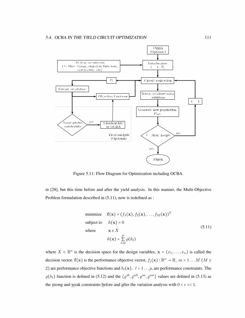
5.4. OCBA IN THE YIELD CIRCUIT OPTIMIZATION 111
Figure 5.11: Flow Diagram for Optimization including OCBA.
in [28], but this time before and after the yield analysis. In this manner, the Multi-Objective
Problem formulation described in (5.11), now is redefined as :
minimize f(x) = (f1(x), f2(x), . . . , fM(x))T
subject to h(x) = 0
where x ∈X
h(x) =p
∑l=0%(hl)
(5.11)
where X ⊂ Rn is the decision space for the design variables, x = (x1, . . . , xn) is called the
decision vector. f(x) is the performance objective vector, fj(x) ∶ Rn → R, m = 1 . . .M (M ≥
2) are performance objective functions and hl(x), l = 1 . . . p, are performance constraints. The
%(hl) function is defined in (5.12) and the %sb, %wb, %sa, %wa values are defined in (5.13) as
the strong and weak constraints before and after the variation analysis with 0 < ε << 1.
112 CHAPTER 5. CIRCUIT VARIATION ANALYSIS
%(hl) = max%sb, %wb, %sa, %wa. (5.12)
%sb =∞, if hl does not accomplish a strong constraint before variation analysis. (5.13a)
%wb = ε, if hl does not accomplish a weak constraint before variation analysis. (5.13b)
%sa = −ε, if hl does not accomplish a strong constraint after variation analysis. (5.13c)
%wa = −∞, if hl does not accomplish a weak constraint after variation analysis. (5.13d)
In our experiments, the strong constraints are the saturation condition in all the transistors
while the weak constraints are the goals in the circuit performances. The %(hl) function always
takes the maximum value among %sb, %wb, %sa, %wa regardless the constraint that are not ac-
complished. Finally, the optimization is accomplished with all the constraints accomplished
before and after the variation analysis (h(x) = 0).
5.4.3 Application Example
There is performed the optimization of the FC OTA exposed before in Chapter 4, however this
time by including a yield analysis. The encoding for the circuit is the same depicted in Table 4.1
and the optimization is performed with the same variables encoding, voltages, current bias and
transistor technology. In our experiments we included the saturation condition in all transistors
as constraints. f(x) is the vector formed by:
f1(x) = -1* Gain .
f2(x) = -1* GBW.
f3(x) = Input referred noise.
f4(x) = Input voltage offset.
f5(x) = Settling time.
f6(x) = -1* Slew rate .
f7(x) = Power consumption.
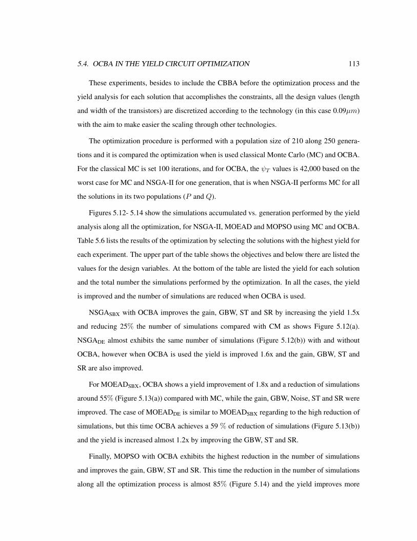
5.4. OCBA IN THE YIELD CIRCUIT OPTIMIZATION 113
These experiments, besides to include the CBBA before the optimization process and the
yield analysis for each solution that accomplishes the constraints, all the design values (length
and width of the transistors) are discretized according to the technology (in this case 0.09µm)
with the aim to make easier the scaling through other technologies.
The optimization procedure is performed with a population size of 210 along 250 genera-
tions and it is compared the optimization when is used classical Monte Carlo (MC) and OCBA.
For the classical MC is set 100 iterations, and for OCBA, the ψT values is 42,000 based on the
worst case for MC and NSGA-II for one generation, that is when NSGA-II performs MC for all
the solutions in its two populations (P and Q).
Figures 5.12- 5.14 show the simulations accumulated vs. generation performed by the yield
analysis along all the optimization, for NSGA-II, MOEAD and MOPSO using MC and OCBA.
Table 5.6 lists the results of the optimization by selecting the solutions with the highest yield for
each experiment. The upper part of the table shows the objectives and below there are listed the
values for the design variables. At the bottom of the table are listed the yield for each solution
and the total number the simulations performed by the optimization. In all the cases, the yield
is improved and the number of simulations are reduced when OCBA is used.
NSGASBX with OCBA improves the gain, GBW, ST and SR by increasing the yield 1.5x
and reducing 25% the number of simulations compared with CM as shows Figure 5.12(a).
NSGADE almost exhibits the same number of simulations (Figure 5.12(b)) with and without
OCBA, however when OCBA is used the yield is improved 1.6x and the gain, GBW, ST and
SR are also improved.
For MOEADSBX, OCBA shows a yield improvement of 1.8x and a reduction of simulations
around 55% (Figure 5.13(a)) compared with MC, while the gain, GBW, Noise, ST and SR were
improved. The case of MOEADDE is similar to MOEADSBX regarding to the high reduction of
simulations, but this time OCBA achieves a 59 % of reduction of simulations (Figure 5.13(b))
and the yield is increased almost 1.2x by improving the GBW, ST and SR.
Finally, MOPSO with OCBA exhibits the highest reduction in the number of simulations
and improves the gain, GBW, ST and SR. This time the reduction in the number of simulations
along all the optimization process is almost 85% (Figure 5.14) and the yield improves more
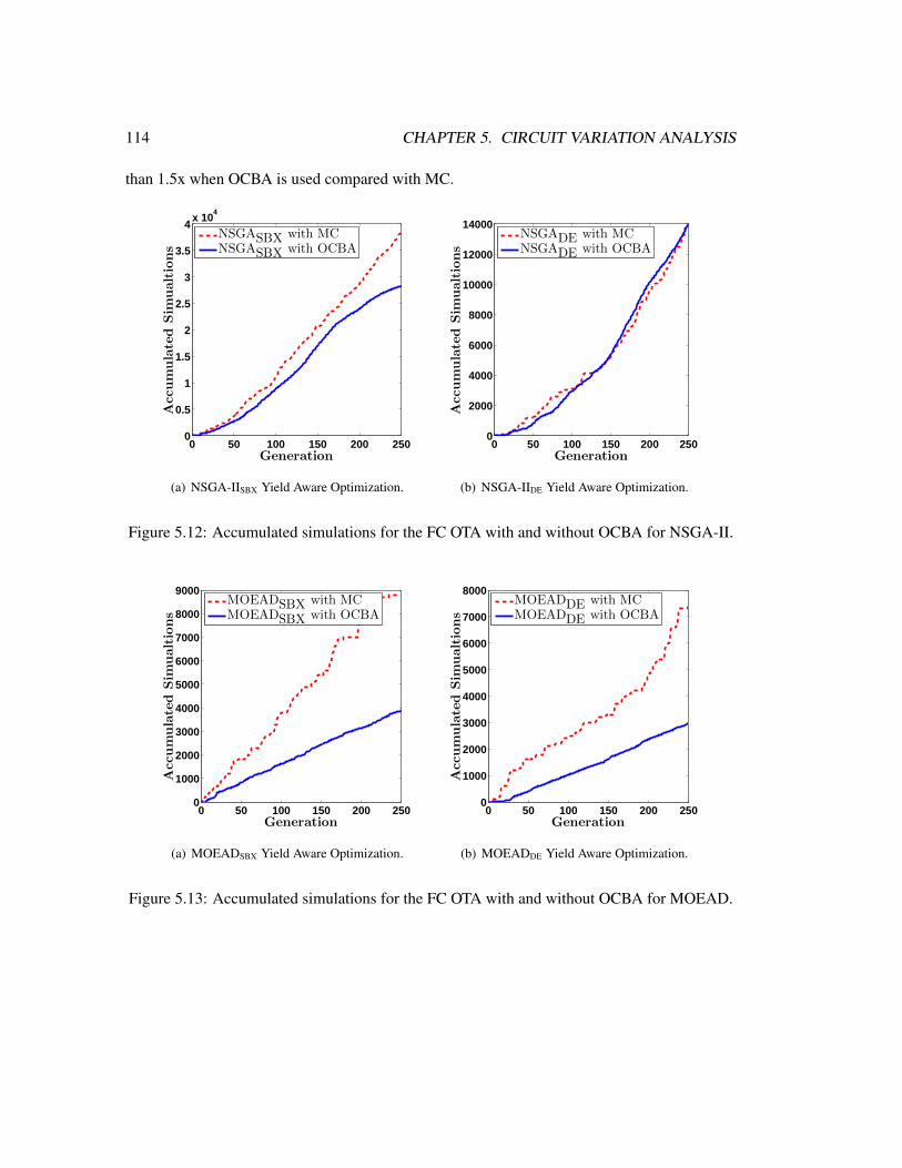
114 CHAPTER 5. CIRCUIT VARIATION ANALYSIS
than 1.5x when OCBA is used compared with MC.
0 50 100 150 200 2500
0.5
1
1.5
2
2.5
3
3.5
4x 10
4
Generation
Accumulated
Sim
ualtions
NSGASBX with MCNSGASBX with OCBA
(a) NSGA-IISBX Yield Aware Optimization.
0 50 100 150 200 2500
2000
4000
6000
8000
10000
12000
14000
GenerationAccumulated
Sim
ualtions
NSGADE with MCNSGADE with OCBA
(b) NSGA-IIDE Yield Aware Optimization.
Figure 5.12: Accumulated simulations for the FC OTA with and without OCBA for NSGA-II.
0 50 100 150 200 2500
1000
2000
3000
4000
5000
6000
7000
8000
9000
Generation
Accumulated
Sim
ualtions
MOEADSBX with MCMOEADSBX with OCBA
(a) MOEADSBX Yield Aware Optimization.
0 50 100 150 200 2500
1000
2000
3000
4000
5000
6000
7000
8000
Generation
Accumulated
Sim
ualtions
MOEADDE with MCMOEADDE with OCBA
(b) MOEADDE Yield Aware Optimization.
Figure 5.13: Accumulated simulations for the FC OTA with and without OCBA for MOEAD.
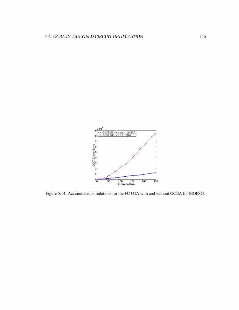
5.4. OCBA IN THE YIELD CIRCUIT OPTIMIZATION 115
0 50 100 150 200 2500
1
2
3
4
5
6
7
8
9x 10
4
Generation
MC
Itera
tions
MOPSO without OCBAMOPSO with OCBA
Figure 5.14: Accumulated simulations for the FC OTA with and without OCBA for MOPSO.
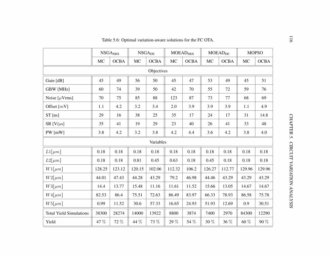
116C
HA
PTE
R5.
CIR
CU
ITVA
RIA
TIO
NA
NA
LYSIS
Table 5.6: Optimal variation-aware solutions for the FC OTA.
NSGASBX NSGADE MOEADSBX MOEADDE MOPSO
MC OCBA MC OCBA MC OCBA MC OCBA MC OCBA
Objectives
Gain [dB] 45 49 56 50 45 47 53 49 45 51
GBW [MHz] 60 74 39 50 42 70 55 72 59 76
Noise [µVrms] 70 75 85 88 123 87 73 77 68 69
Offset [mV] 1.1 4.2 3.2 3.4 2.0 3.9 3.9 3.9 1.1 4.9
ST [ns] 29 16 38 25 35 17 24 17 31 14.8
SR [V/µs] 35 41 19 29 23 40 26 41 33 48
PW [mW] 3.8 4.2 3.2 3.8 4.2 4.4 3.6 4.2 3.8 4.0
Variables
L1[µm] 0.18 0.18 0.18 0.18 0.18 0.18 0.18 0.18 0.18 0.18
L2[µm] 0.18 0.18 0.81 0.45 0.63 0.18 0.45 0.18 0.18 0.18
W1[µm] 128.25 123.12 120.15 102.06 112.32 106.2 126.27 112.77 129.96 129.96
W2[µm] 44.01 47.43 44.28 43.29 79.2 46.98 44.46 43.29 43.29 43.29
W3[µm] 14.4 13.77 15.48 11.16 11.61 11.52 15.66 13.05 14.67 14.67
W4[µm] 82.53 86.4 75.51 72.63 86.49 83.97 66.33 78.93 86.58 75.78
W5[µm] 0.99 11.52 30.6 57.33 16.65 24.93 51.93 12.69 0.9 30.51
Total Yield Simulations 38300 28274 14000 13922 8800 3874 7400 2970 84300 12290
Yield 47 % 72 % 44 % 73 % 29 % 54 % 30 % 36 % 60 % 90 %
5.5. SUMMARY 117
5.5 Summary
This Chapter was devoted to explore the variation aware optimization of analog circuits. The
variation analysis is an important decision point because before this analysis, all the target
specifications are accomplished but if we select those solutions without taking into account
their variations, in the fabrication process there is a strong possibility that the designed circuits
do not guarantee optimal performances. In this manner, it is important to be able to discriminate
those solutions that are not really feasible.
The use of finite differences and Richardson extrapolation allows us to calculate the partial
derivatives for multi-parameter sensitivity analysis, without an explicit mathematical expres-
sion. Our proposed approach based on the multi-parameter sensitivity was tested on the RFC
OTA, and there were found the best solutions that accomplish all the target specifications for
each objective and they improve the performances already published in [99] with the lowest
multi-parameter sensitivity.
The shortcomings of this approach are related with the fact that the number of sensitivities
increase dramatically with the number of design variables or circuit performances. Also this
approach may be stalled when it is desired to find more accurate results, due to the significant
digits that the simulator can handle.
Also, it has been performed a Non-Worst case approach based on MC simulations by intro-
ducing an optimal simulation budget allocation technique called OCBA. We showed that this
approach allows always improving the yield and sometimes reducing the number of simulations
required for a typical MC approach in the optimization of analog circuits with EAs.
The shortcoming of this approach is that it requires the transistor models form the factory
and the complexity of these models and the number of simulations exhibit a strong dependence
on the accuracy. To overcome the issue of the efficiency in this sort of methodology, the OCBA
approach has shown an alternative reducing the number of simulations up to 85% and improv-
ing the yield up to 1.8x compared with a classical MC technique. For introducing the OCBA
into the circuit optimization the only extra parameters are the maximum and initial number of
simulations for the yield analysis.

118 CHAPTER 5. CIRCUIT VARIATION ANALYSIS

Chapter 6
Conclusions
The analog circuit biasing and sizing can be considered as a non-linear problem with multiple
objectives, dozens of variables and many constraints. The analog designers need to invest a lot
of time to gain enough experience in a given circuit to accomplish all the design requirements.
Furthermore, after a design is biased and sized properly, the process variations in the fabrication
of that design might make that it can be rejected because its low tolerance to variations. A useful
tool to cope with this complex problem is the use of EDA optimization tools. Those tools are
devoted to help to the designers to gain insight into a design, find its limitations and ensure that
the selected design is a feasible one because accomplish all the requirements.
Although several optimization tools exist both in the academic and industrial fields, that
solve circuit biasing and sizing issues, they still have to overcome some design shortcomings.
For instance, EDA tools have been developed for designing a specific set of circuits and also
by optimizing a specific set of objectives. Some of them lost accuracy while improving their
efficiency by using behavioral models. Besides, when compared with a circuit simulator their
results may differ. Not all EDA tools are able to handle any transistor model and or technol-
ogy, neither to include a process variations procedure to ensure feasible solutions. To cope
with these circuit design challenges, this Thesis showed that EAs are a good choice to per-
form circuit optimization. Three EAs were described and applied, namely: NSGA-II, MOEAD
and MOPSO. Along the chapters, several optimization examples were presented for different
circuits to highlight the flexibility and suitability of EAs in varying the number of optimized
119
120 CHAPTER 6. CONCLUSIONS
variables, constraints and objectives. Also, those experiments were performed with different
transistor models and technologies, with any extra programming. All the results provided by
EAs are trustworthy because they become directly from the circuit simulator, then all the accu-
racy depends on the simulator accuracy. By comparing the performance of each EA along all
the examples, it is possible to notice that there is no algorithm superior to other.
However, the circuit optimization still requires a continuing search process to finding biased
solutions, because it is not possible to optimize the circuit performances while not having biased
solutions. This process depends strongly of the initial search space and may invest a lot of time.
In this manner, this Thesis introduced a CBBA method where the basic idea is to choose the
appropriate limits over the search space for the encoded variables in the sizing process that takes
place in the analog circuit optimization. In this manner, it can be possible to achieve a successful
optimization without having a deep insight in the circuit and without waste of time on searching
values that are not feasible due to the wrong biasing of the circuit. To show the usefulness of the
CBBA, there were presented circuit optimization examples performed with NSGA-II, MOEAD
and MOPSO and finding that CBBA helps to accomplish the objective specifications compared
when CBBA is not used and/or reduce the number of generations required to find an optimal
solution.
Regarding to the process variation analysis into the circuit optimization, there were exposed
two different approaches devoted to incorporate a Non-Worst case methodology taking into ac-
count the fabrication process variations, showing again the flexibility of the EAs to incorporate
extra modules. The first method is based on the multi-parameter sensitivity of the circuit de-
vices and the second one is based on MC simulations by using the OCBA approach to improve
the yield and reducing the number of simulations required to achieve the optimization.
The use of EDA tools usually is highly impacted by three factors: the operating system,
the simulator and the software interface. Those issues were taken into account to develop a
software tool that gathers all the advantages of EAs, CBBA and OCBA to the optimization of
analog circuits. In this Thesis a software tool was developed with PERL which is an open source
language available for the most common operating systems. In the same direction, an evalua-
tion module was programmed to perform the circuit simulations with any simulator having an
121
output file with the circuit measurements. Finally, the developed GUI facilitates its use for the
analog circuit designers allowing entering all the optimization parameters and performing the
optimization all on the same screen.
It is possible to summarize the next contributions:
• A multi-EA circuit optimizer platform.
• Highest-quality circuit performance tradeoffs.
• A new current-branches-bias assignment (CBBA) approach has been introduced in order
to accelerate the sizing process of an analog integrated circuit composed of MOSFETs.
• Minimizing computational effort in the multi-objective analog circuit optimization by
using OCBA.
• A portable software for analog circuit optimization based on EAs.
As a conclusion, we believe that the proposed approach is a powerful tool to enhance analog
circuit design through generating feasible solutions accomplishing target specifications, with the
possibility of improving the results and the efficiency by using the CBBA and OCBA methods.
Also, it is possible to choose among different variables encodings, to explore the best per-
formances of an analog IC, and including support variations so that the optimal performance of
a circuit design can be guaranteed.
Finally, as the main future work, it is possible to highlight the research on the local and
global optimization for reducing the run time and the use of design of experiments such as
Latin Hypercube or Quasi-Monte Carlo with the aim to reduce the number of simulations for
the yield optimization.

122 CHAPTER 6. CONCLUSIONS

Appendix A
Circuit Optimizer Software Tool
This section is devoted to show the circuit optimizer software tool developed to perform all the
circuit optimizations in this Thesis. The software tool is composed by the code of NSGA-II,
MOEAD and MOPSO adapted for the circuit optimization and able to choose the use of CBBA
and/or yield analysis (performed with classical Monte Carlo or OCBA). Figure A.1 shows the
main modules on the left side and on the right side shows the inputs to each module. The
general parameters are the population size and the maximum number of generations. The CBBA
module needs the circuit netlist and this module can be optional. The initialization module is
devoted to generate the first population where each variable is delimited by a minimum and
maximum value (in the case that CBBA is executed, the bounds of some variables are modified
according to the different current branches). The optimization module selects an EA (NSGA-II,
MOEAD or MOPSO) and a recombination operator (SBX or DE), according with these choices
are set different parameters. The sub-module of circuit simulation requires the circuit netlist,
the objective functions, the constraints and the circuit simulator. Finally the sub-module of yield
analysis is optional but requires the circuit netlist adapted to Monte Carlo simulations, choosing
between classical Monte Carlo or OCBA analysis and a maximum number of iterations for the
yield analysis.
In this manner the software developed, links all the modules with its input parameters mak-
ing easier to perform a circuit optimization without programming and by feeding all the pa-
rameters. The graphical interface was programmed with TCL and all the optimization is pro-
123
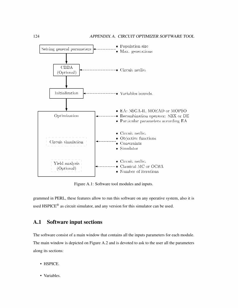
124 APPENDIX A. CIRCUIT OPTIMIZER SOFTWARE TOOL
Figure A.1: Software tool modules and inputs.
grammed in PERL, these features allow to run this software on any operative system, also it is
used HSPICE® as circuit simulator, and any version for this simulator can be used.
A.1 Software input sections
The software consist of a main window that contains all the inputs parameters for each module.
The main window is depicted on Figure A.2 and is devoted to ask to the user all the parameters
along its sections:
• HSPICE.
• Variables.
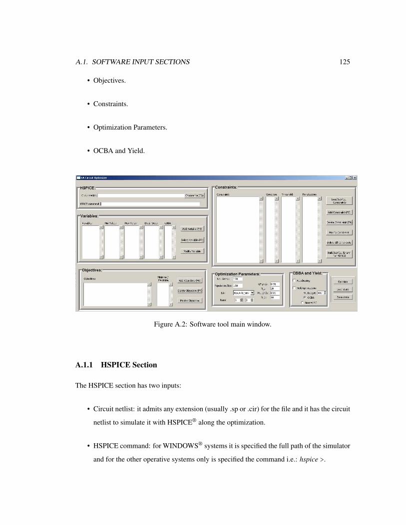
A.1. SOFTWARE INPUT SECTIONS 125
• Objectives.
• Constraints.
• Optimization Parameters.
• OCBA and Yield.
Figure A.2: Software tool main window.
A.1.1 HSPICE Section
The HSPICE section has two inputs:
• Circuit netlist: it admits any extension (usually .sp or .cir) for the file and it has the circuit
netlist to simulate it with HSPICE® along the optimization.
• HSPICE command: for WINDOWS® systems it is specified the full path of the simulator
and for the other operative systems only is specified the command i.e.: hspice >.

126 APPENDIX A. CIRCUIT OPTIMIZER SOFTWARE TOOL
Figure A.3: HSPICE section.
A.1.2 Variables Section
The variables section allows adding, modifying or deleting variables. It has five inputs as shows
Figure A.4 and the order how appear the variables here is the same order that is going to be
displayed for the simulator:
• Variable: variable name, it can be any combination of characters and it is used to identify
the variable.
• Min Value: the minimum limit value for the variable for both, the initialization and the
optimization.
• Max Value: the maximum limit value for the variable for both, the initialization and the
optimization.
• Discr. Step: if it is desired that the variables accomplish discrete values, it accepts any
value and for continuos variables can be set a very small value as 1E − 10.
• CBBA: if the variable is going to be partitioned with the CBBA procedure.
To add a new variable there are required the five inputs as shows Figure A.5 where the
variable name is W1 (it represents the width of some transistors in the netlist), and 0.9µm ≤
W1 ≤ 130µm with 0.09µm as discrete step, and it is desired that this variable has partitioned
by the CBBA procedure.
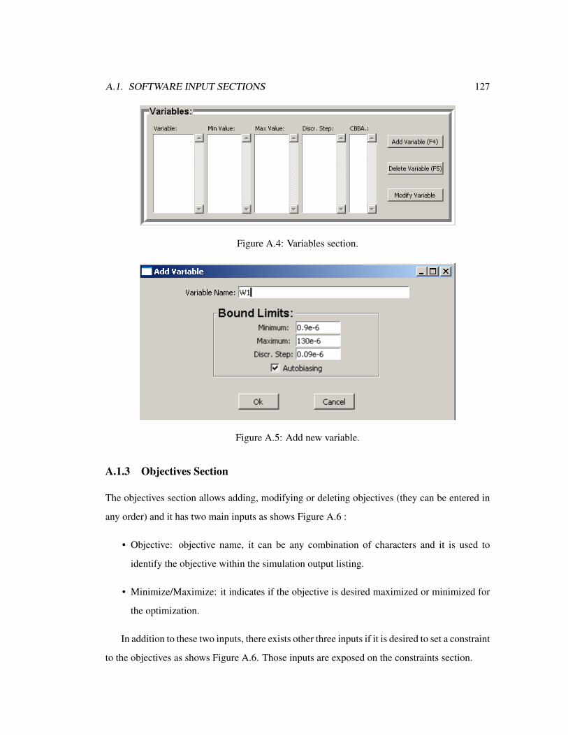
A.1. SOFTWARE INPUT SECTIONS 127
Figure A.4: Variables section.
Figure A.5: Add new variable.
A.1.3 Objectives Section
The objectives section allows adding, modifying or deleting objectives (they can be entered in
any order) and it has two main inputs as shows Figure A.6 :
• Objective: objective name, it can be any combination of characters and it is used to
identify the objective within the simulation output listing.
• Minimize/Maximize: it indicates if the objective is desired maximized or minimized for
the optimization.
In addition to these two inputs, there exists other three inputs if it is desired to set a constraint
to the objectives as shows Figure A.6. Those inputs are exposed on the constraints section.
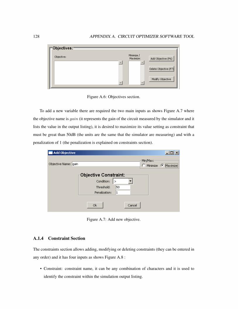
128 APPENDIX A. CIRCUIT OPTIMIZER SOFTWARE TOOL
Figure A.6: Objectives section.
To add a new variable there are required the two main inputs as shows Figure A.7 where
the objective name is gain (it represents the gain of the circuit measured by the simulator and it
lists the value in the output listing), it is desired to maximize its value setting as constraint that
must be great than 50dB (the units are the same that the simulator are measuring) and with a
penalization of 1 (the penalization is explained on constraints section).
Figure A.7: Add new objective.
A.1.4 Constraint Section
The constraints section allows adding, modifying or deleting constraints (they can be entered in
any order) and it has four inputs as shows Figure A.8 :
• Constraint: constraint name, it can be any combination of characters and it is used to
identify the constraint within the simulation output listing.

A.1. SOFTWARE INPUT SECTIONS 129
• Condition: it indicates if the constraints must be less or greater than a threshold value.
• Threshold: it is the threshold value for the constraint condition.
• Penalization: it is the value which penalizes when a constraint is not accomplished. In
general all the constraints can have the same penalization value, however it is possible
to handling different values with the aim to identify among different constraint hierarchy
levels, for instance, the saturation of the transistors can have a great value (i.e. 100)
because has a higher hierarchy level than others as objective constraint that have less
values (i.e. 1).
Figure A.8: Constraints section.
To add a new constraint there are required the four inputs as shows Figure A.9 where the
objective name is gain (it represents the gain of the circuit measured by the simulator and it
lists the value in the output listing), it must be greater than 50dB (the units are the same that the
simulator are measuring) and with a penalization of 1.
There exist other two options in this section related to the saturation and lineal condition of
the transistors constraints:
• Load Sat/Cut Constraints: with this option, all the saturation and lineal of transistor con-
straints are entered in the list of constraints from the circuit netlist. This option automat-
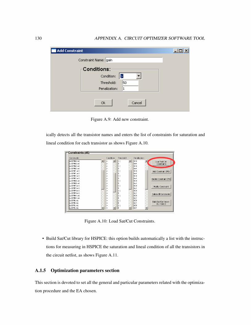
130 APPENDIX A. CIRCUIT OPTIMIZER SOFTWARE TOOL
Figure A.9: Add new constraint.
ically detects all the transistor names and enters the list of constraints for saturation and
lineal condition for each transistor as shows Figure A.10.
Figure A.10: Load Sat/Cut Constraints.
• Build Sat/Cut library for HSPICE: this option builds automatically a list with the instruc-
tions for measuring in HSPICE the saturation and lineal condition of all the transistors in
the circuit netlist, as shows Figure A.11.
A.1.5 Optimization parameters section
This section is devoted to set all the general and particular parameters related with the optimiza-
tion procedure and the EA chosen.
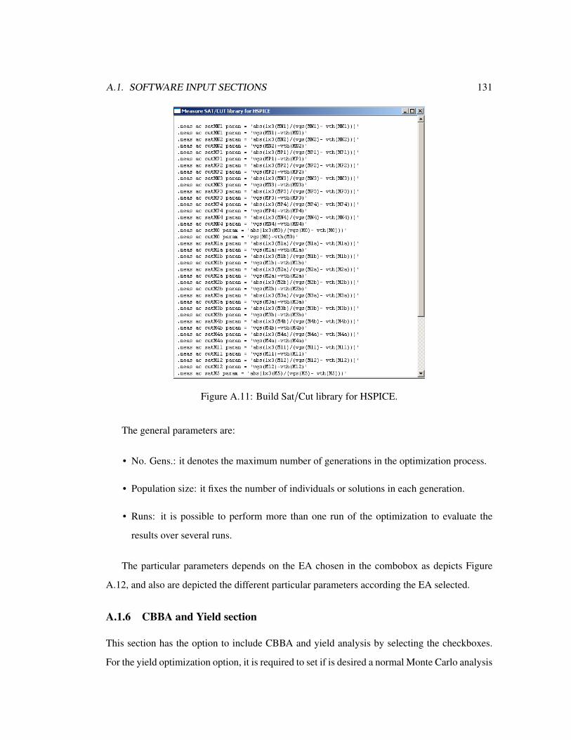
A.1. SOFTWARE INPUT SECTIONS 131
Figure A.11: Build Sat/Cut library for HSPICE.
The general parameters are:
• No. Gens.: it denotes the maximum number of generations in the optimization process.
• Population size: it fixes the number of individuals or solutions in each generation.
• Runs: it is possible to perform more than one run of the optimization to evaluate the
results over several runs.
The particular parameters depends on the EA chosen in the combobox as depicts Figure
A.12, and also are depicted the different particular parameters according the EA selected.
A.1.6 CBBA and Yield section
This section has the option to include CBBA and yield analysis by selecting the checkboxes.
For the yield optimization option, it is required to set if is desired a normal Monte Carlo analysis
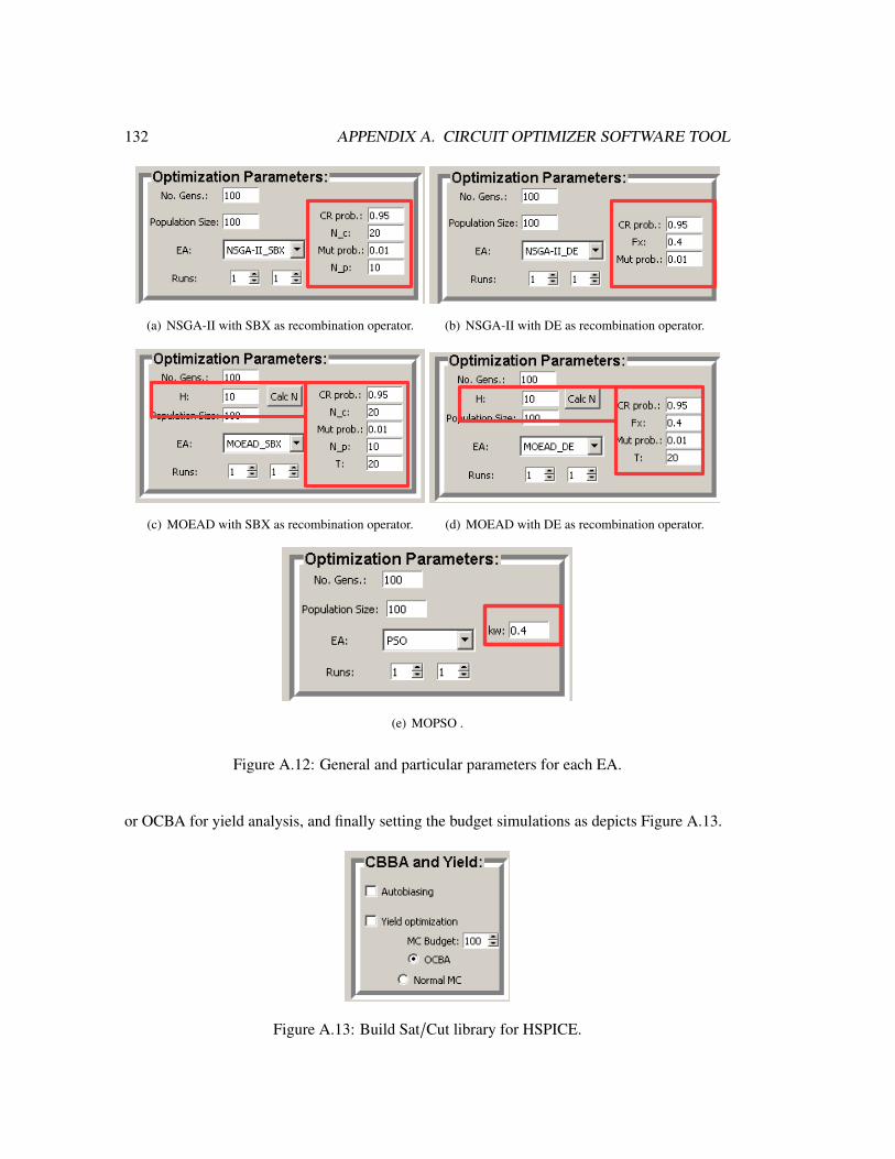
132 APPENDIX A. CIRCUIT OPTIMIZER SOFTWARE TOOL
(a) NSGA-II with SBX as recombination operator. (b) NSGA-II with DE as recombination operator.
(c) MOEAD with SBX as recombination operator. (d) MOEAD with DE as recombination operator.
(e) MOPSO .
Figure A.12: General and particular parameters for each EA.
or OCBA for yield analysis, and finally setting the budget simulations as depicts Figure A.13.
Figure A.13: Build Sat/Cut library for HSPICE.

A.2. BUTTONS SECTION 133
A.2 Buttons section
This is the last section in the software tool and has three buttons:
• Optimize: this button starts the optimization with all the inputs in all the sections by
displaying the current generation and the best penalization in the current optimization to
get an idea about the current optimization, the optimization objective is to find the less
penalization ( it is desired zero penalization).
• Load State: this button allows to load previous inputs in all the sections .
• Save State: this button allows to save into a file the current inputs of all the sections.
A.3 Software output
The final result of a optimization are a set of files, all of them called as the circuit netlist file
as prefix (File Name) and the number of run as suffix (the number 1 represents the first run,
the number 2 represents the second and so on), which contains the results of the optimization
(values, function objectives, penalization, yields). Next it is exposed the contents of each file
for the first run:
• File Name R1.rw: it has all the historic of all individuals over all the generations.
• File Name R1 aux.rw: it has all the historic of all individuals of the last generation as
backup to continue the optimization in case of necessary.
• File Name REP1.rw: it lists the best solutions for each generation.
• File Name OUT.rw: it lists all the best solutions of the last generation.

134 APPENDIX A. CIRCUIT OPTIMIZER SOFTWARE TOOL
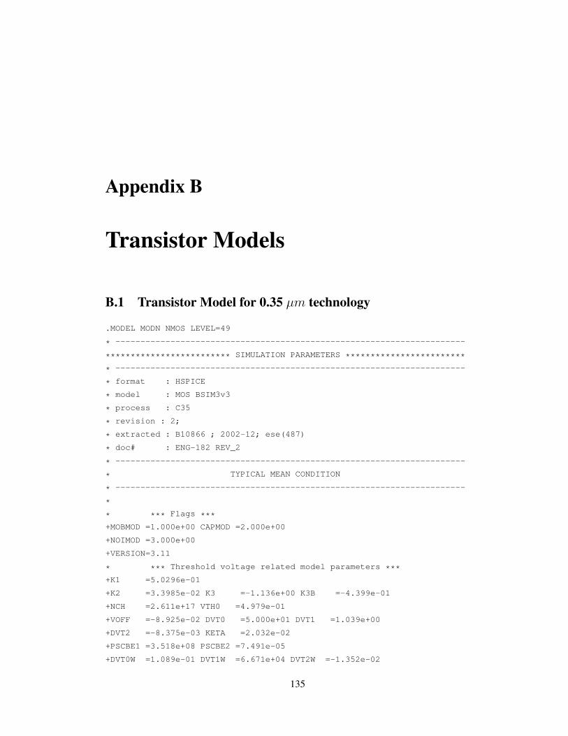
Appendix B
Transistor Models
B.1 Transistor Model for 0.35 µm technology
.MODEL MODN NMOS LEVEL=49
* ----------------------------------------------------------------------
************************* SIMULATION PARAMETERS ************************
* ----------------------------------------------------------------------
* format : HSPICE
* model : MOS BSIM3v3
* process : C35
* revision : 2;
* extracted : B10866 ; 2002-12; ese(487)
* doc# : ENG-182 REV_2
* ----------------------------------------------------------------------
* TYPICAL MEAN CONDITION
* ----------------------------------------------------------------------
*
* *** Flags ***
+MOBMOD =1.000e+00 CAPMOD =2.000e+00
+NOIMOD =3.000e+00
+VERSION=3.11
* *** Threshold voltage related model parameters ***
+K1 =5.0296e-01
+K2 =3.3985e-02 K3 =-1.136e+00 K3B =-4.399e-01
+NCH =2.611e+17 VTH0 =4.979e-01
+VOFF =-8.925e-02 DVT0 =5.000e+01 DVT1 =1.039e+00
+DVT2 =-8.375e-03 KETA =2.032e-02
+PSCBE1 =3.518e+08 PSCBE2 =7.491e-05
+DVT0W =1.089e-01 DVT1W =6.671e+04 DVT2W =-1.352e-02
135
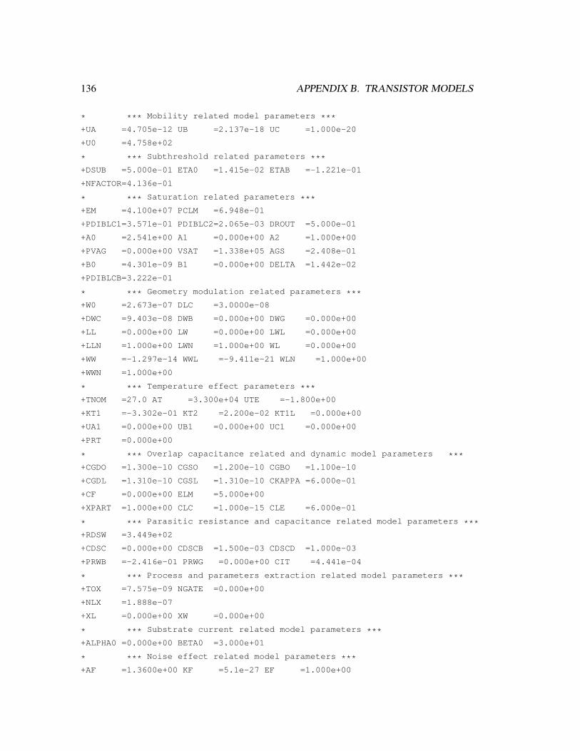
136 APPENDIX B. TRANSISTOR MODELS
* *** Mobility related model parameters ***
+UA =4.705e-12 UB =2.137e-18 UC =1.000e-20
+U0 =4.758e+02
* *** Subthreshold related parameters ***
+DSUB =5.000e-01 ETA0 =1.415e-02 ETAB =-1.221e-01
+NFACTOR=4.136e-01
* *** Saturation related parameters ***
+EM =4.100e+07 PCLM =6.948e-01
+PDIBLC1=3.571e-01 PDIBLC2=2.065e-03 DROUT =5.000e-01
+A0 =2.541e+00 A1 =0.000e+00 A2 =1.000e+00
+PVAG =0.000e+00 VSAT =1.338e+05 AGS =2.408e-01
+B0 =4.301e-09 B1 =0.000e+00 DELTA =1.442e-02
+PDIBLCB=3.222e-01
* *** Geometry modulation related parameters ***
+W0 =2.673e-07 DLC =3.0000e-08
+DWC =9.403e-08 DWB =0.000e+00 DWG =0.000e+00
+LL =0.000e+00 LW =0.000e+00 LWL =0.000e+00
+LLN =1.000e+00 LWN =1.000e+00 WL =0.000e+00
+WW =-1.297e-14 WWL =-9.411e-21 WLN =1.000e+00
+WWN =1.000e+00
* *** Temperature effect parameters ***
+TNOM =27.0 AT =3.300e+04 UTE =-1.800e+00
+KT1 =-3.302e-01 KT2 =2.200e-02 KT1L =0.000e+00
+UA1 =0.000e+00 UB1 =0.000e+00 UC1 =0.000e+00
+PRT =0.000e+00
* *** Overlap capacitance related and dynamic model parameters ***
+CGDO =1.300e-10 CGSO =1.200e-10 CGBO =1.100e-10
+CGDL =1.310e-10 CGSL =1.310e-10 CKAPPA =6.000e-01
+CF =0.000e+00 ELM =5.000e+00
+XPART =1.000e+00 CLC =1.000e-15 CLE =6.000e-01
* *** Parasitic resistance and capacitance related model parameters ***
+RDSW =3.449e+02
+CDSC =0.000e+00 CDSCB =1.500e-03 CDSCD =1.000e-03
+PRWB =-2.416e-01 PRWG =0.000e+00 CIT =4.441e-04
* *** Process and parameters extraction related model parameters ***
+TOX =7.575e-09 NGATE =0.000e+00
+NLX =1.888e-07
+XL =0.000e+00 XW =0.000e+00
* *** Substrate current related model parameters ***
+ALPHA0 =0.000e+00 BETA0 =3.000e+01
* *** Noise effect related model parameters ***
+AF =1.3600e+00 KF =5.1e-27 EF =1.000e+00
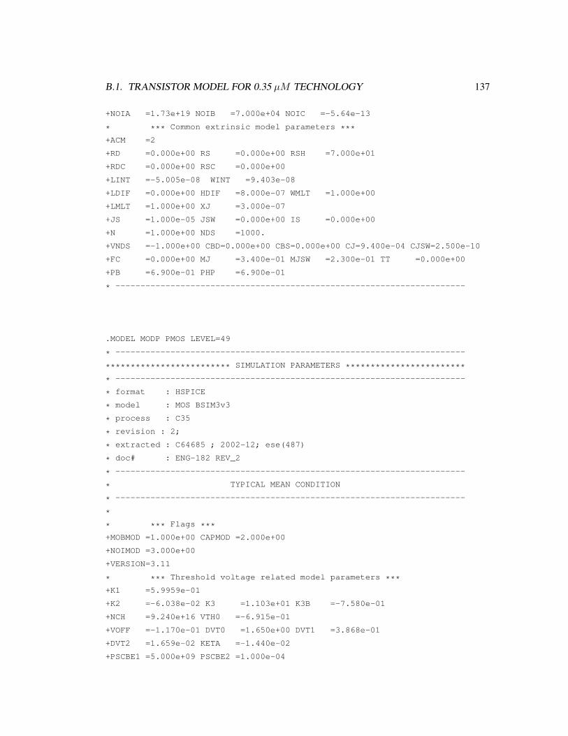
B.1. TRANSISTOR MODEL FOR 0.35 µM TECHNOLOGY 137
+NOIA =1.73e+19 NOIB =7.000e+04 NOIC =-5.64e-13
* *** Common extrinsic model parameters ***
+ACM =2
+RD =0.000e+00 RS =0.000e+00 RSH =7.000e+01
+RDC =0.000e+00 RSC =0.000e+00
+LINT =-5.005e-08 WINT =9.403e-08
+LDIF =0.000e+00 HDIF =8.000e-07 WMLT =1.000e+00
+LMLT =1.000e+00 XJ =3.000e-07
+JS =1.000e-05 JSW =0.000e+00 IS =0.000e+00
+N =1.000e+00 NDS =1000.
+VNDS =-1.000e+00 CBD=0.000e+00 CBS=0.000e+00 CJ=9.400e-04 CJSW=2.500e-10
+FC =0.000e+00 MJ =3.400e-01 MJSW =2.300e-01 TT =0.000e+00
+PB =6.900e-01 PHP =6.900e-01
* ----------------------------------------------------------------------
.MODEL MODP PMOS LEVEL=49
* ----------------------------------------------------------------------
************************* SIMULATION PARAMETERS ************************
* ----------------------------------------------------------------------
* format : HSPICE
* model : MOS BSIM3v3
* process : C35
* revision : 2;
* extracted : C64685 ; 2002-12; ese(487)
* doc# : ENG-182 REV_2
* ----------------------------------------------------------------------
* TYPICAL MEAN CONDITION
* ----------------------------------------------------------------------
*
* *** Flags ***
+MOBMOD =1.000e+00 CAPMOD =2.000e+00
+NOIMOD =3.000e+00
+VERSION=3.11
* *** Threshold voltage related model parameters ***
+K1 =5.9959e-01
+K2 =-6.038e-02 K3 =1.103e+01 K3B =-7.580e-01
+NCH =9.240e+16 VTH0 =-6.915e-01
+VOFF =-1.170e-01 DVT0 =1.650e+00 DVT1 =3.868e-01
+DVT2 =1.659e-02 KETA =-1.440e-02
+PSCBE1 =5.000e+09 PSCBE2 =1.000e-04
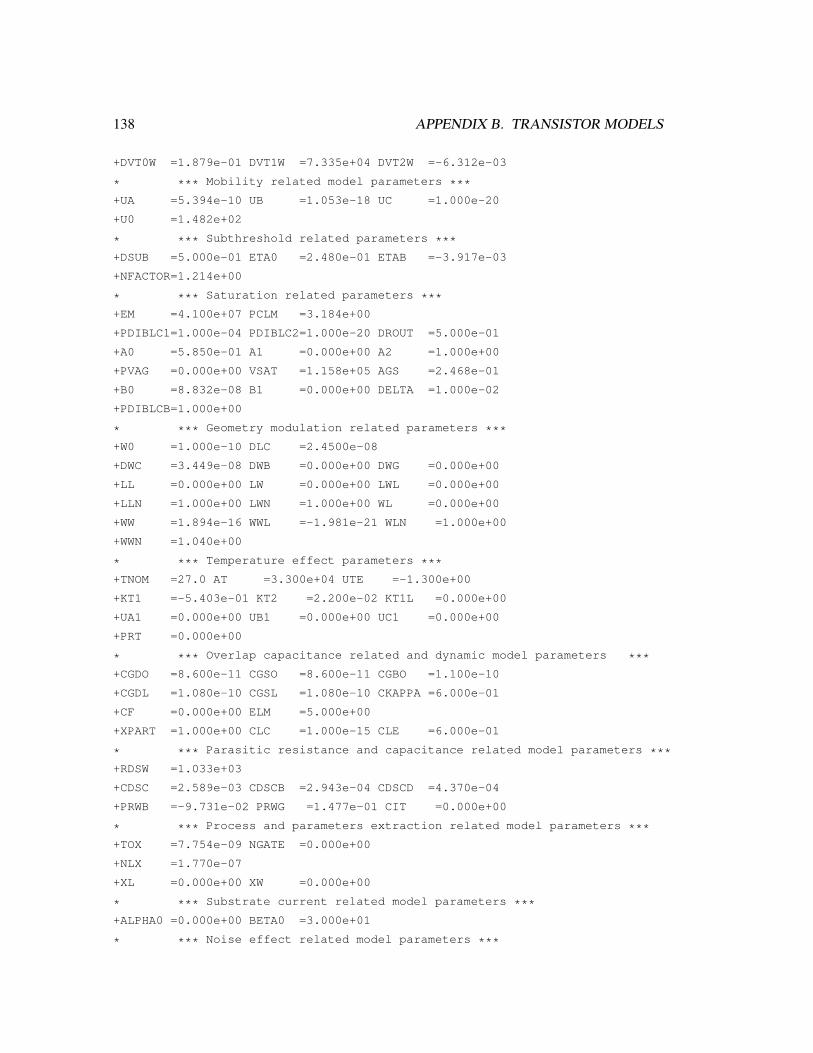
138 APPENDIX B. TRANSISTOR MODELS
+DVT0W =1.879e-01 DVT1W =7.335e+04 DVT2W =-6.312e-03
* *** Mobility related model parameters ***
+UA =5.394e-10 UB =1.053e-18 UC =1.000e-20
+U0 =1.482e+02
* *** Subthreshold related parameters ***
+DSUB =5.000e-01 ETA0 =2.480e-01 ETAB =-3.917e-03
+NFACTOR=1.214e+00
* *** Saturation related parameters ***
+EM =4.100e+07 PCLM =3.184e+00
+PDIBLC1=1.000e-04 PDIBLC2=1.000e-20 DROUT =5.000e-01
+A0 =5.850e-01 A1 =0.000e+00 A2 =1.000e+00
+PVAG =0.000e+00 VSAT =1.158e+05 AGS =2.468e-01
+B0 =8.832e-08 B1 =0.000e+00 DELTA =1.000e-02
+PDIBLCB=1.000e+00
* *** Geometry modulation related parameters ***
+W0 =1.000e-10 DLC =2.4500e-08
+DWC =3.449e-08 DWB =0.000e+00 DWG =0.000e+00
+LL =0.000e+00 LW =0.000e+00 LWL =0.000e+00
+LLN =1.000e+00 LWN =1.000e+00 WL =0.000e+00
+WW =1.894e-16 WWL =-1.981e-21 WLN =1.000e+00
+WWN =1.040e+00
* *** Temperature effect parameters ***
+TNOM =27.0 AT =3.300e+04 UTE =-1.300e+00
+KT1 =-5.403e-01 KT2 =2.200e-02 KT1L =0.000e+00
+UA1 =0.000e+00 UB1 =0.000e+00 UC1 =0.000e+00
+PRT =0.000e+00
* *** Overlap capacitance related and dynamic model parameters ***
+CGDO =8.600e-11 CGSO =8.600e-11 CGBO =1.100e-10
+CGDL =1.080e-10 CGSL =1.080e-10 CKAPPA =6.000e-01
+CF =0.000e+00 ELM =5.000e+00
+XPART =1.000e+00 CLC =1.000e-15 CLE =6.000e-01
* *** Parasitic resistance and capacitance related model parameters ***
+RDSW =1.033e+03
+CDSC =2.589e-03 CDSCB =2.943e-04 CDSCD =4.370e-04
+PRWB =-9.731e-02 PRWG =1.477e-01 CIT =0.000e+00
* *** Process and parameters extraction related model parameters ***
+TOX =7.754e-09 NGATE =0.000e+00
+NLX =1.770e-07
+XL =0.000e+00 XW =0.000e+00
* *** Substrate current related model parameters ***
+ALPHA0 =0.000e+00 BETA0 =3.000e+01
* *** Noise effect related model parameters ***
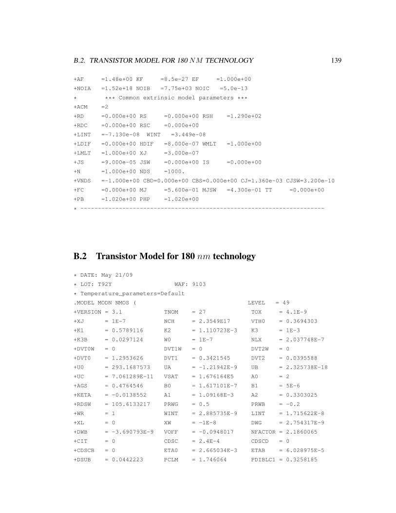
B.2. TRANSISTOR MODEL FOR 180 NM TECHNOLOGY 139
+AF =1.48e+00 KF =8.5e-27 EF =1.000e+00
+NOIA =1.52e+18 NOIB =7.75e+03 NOIC =5.0e-13
* *** Common extrinsic model parameters ***
+ACM =2
+RD =0.000e+00 RS =0.000e+00 RSH =1.290e+02
+RDC =0.000e+00 RSC =0.000e+00
+LINT =-7.130e-08 WINT =3.449e-08
+LDIF =0.000e+00 HDIF =8.000e-07 WMLT =1.000e+00
+LMLT =1.000e+00 XJ =3.000e-07
+JS =9.000e-05 JSW =0.000e+00 IS =0.000e+00
+N =1.000e+00 NDS =1000.
+VNDS =-1.000e+00 CBD=0.000e+00 CBS=0.000e+00 CJ=1.360e-03 CJSW=3.200e-10
+FC =0.000e+00 MJ =5.600e-01 MJSW =4.300e-01 TT =0.000e+00
+PB =1.020e+00 PHP =1.020e+00
* ----------------------------------------------------------------------
B.2 Transistor Model for 180 nm technology
* DATE: May 21/09
* LOT: T92Y WAF: 9103
* Temperature_parameters=Default
.MODEL MODN NMOS ( LEVEL = 49
+VERSION = 3.1 TNOM = 27 TOX = 4.1E-9
+XJ = 1E-7 NCH = 2.3549E17 VTH0 = 0.3694303
+K1 = 0.5789116 K2 = 1.110723E-3 K3 = 1E-3
+K3B = 0.0297124 W0 = 1E-7 NLX = 2.037748E-7
+DVT0W = 0 DVT1W = 0 DVT2W = 0
+DVT0 = 1.2953626 DVT1 = 0.3421545 DVT2 = 0.0395588
+U0 = 293.1687573 UA = -1.21942E-9 UB = 2.325738E-18
+UC = 7.061289E-11 VSAT = 1.676164E5 A0 = 2
+AGS = 0.4764546 B0 = 1.617101E-7 B1 = 5E-6
+KETA = -0.0138552 A1 = 1.09168E-3 A2 = 0.3303025
+RDSW = 105.6133217 PRWG = 0.5 PRWB = -0.2
+WR = 1 WINT = 2.885735E-9 LINT = 1.715622E-8
+XL = 0 XW = -1E-8 DWG = 2.754317E-9
+DWB = -3.690793E-9 VOFF = -0.0948017 NFACTOR = 2.1860065
+CIT = 0 CDSC = 2.4E-4 CDSCD = 0
+CDSCB = 0 ETA0 = 2.665034E-3 ETAB = 6.028975E-5
+DSUB = 0.0442223 PCLM = 1.746064 PDIBLC1 = 0.3258185
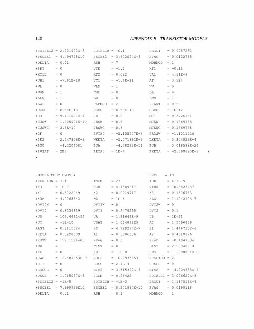
140 APPENDIX B. TRANSISTOR MODELS
+PDIBLC2 = 2.701992E-3 PDIBLCB = -0.1 DROUT = 0.9787232
+PSCBE1 = 4.494778E10 PSCBE2 = 3.672074E-8 PVAG = 0.0122755
+DELTA = 0.01 RSH = 7 MOBMOD = 1
+PRT = 0 UTE = -1.5 KT1 = -0.11
+KT1L = 0 KT2 = 0.022 UA1 = 4.31E-9
+UB1 = -7.61E-18 UC1 = -5.6E-11 AT = 3.3E4
+WL = 0 WLN = 1 WW = 0
+WWN = 1 WWL = 0 LL = 0
+LLN = 1 LW = 0 LWN = 1
+LWL = 0 CAPMOD = 2 XPART = 0.5
+CGDO = 8.58E-10 CGSO = 8.58E-10 CGBO = 1E-12
+CJ = 9.471097E-4 PB = 0.8 MJ = 0.3726161
+CJSW = 1.905901E-10 PBSW = 0.8 MJSW = 0.1369758
+CJSWG = 3.3E-10 PBSWG = 0.8 MJSWG = 0.1369758
+CF = 0 PVTH0 = -5.105777E-3 PRDSW = -1.1011726
+PK2 = 2.247806E-3 WKETA = -5.071892E-3 LKETA = 5.324922E-4
+PU0 = -4.0206081 PUA = -4.48232E-11 PUB = 5.018589E-24
+PVSAT = 2E3 PETA0 = 1E-4 PKETA = -2.090695E-3 )
*
.MODEL MODP PMOS ( LEVEL = 49
+VERSION = 3.1 TNOM = 27 TOX = 4.1E-9
+XJ = 1E-7 NCH = 4.1589E17 VTH0 = -0.3823437
+K1 = 0.5722049 K2 = 0.0219717 K3 = 0.1576753
+K3B = 4.2763642 W0 = 1E-6 NLX = 1.104212E-7
+DVT0W = 0 DVT1W = 0 DVT2W = 0
+DVT0 = 0.6234839 DVT1 = 0.2479255 DVT2 = 0.1
+U0 = 109.4682454 UA = 1.31646E-9 UB = 1E-21
+UC = -1E-10 VSAT = 1.054892E5 A0 = 1.5796859
+AGS = 0.3115024 B0 = 4.729297E-7 B1 = 1.446715E-6
+KETA = 0.0298609 A1 = 0.3886886 A2 = 0.4010376
+RDSW = 199.1594405 PRWG = 0.5 PRWB = -0.4947034
+WR = 1 WINT = 0 LINT = 2.93948E-8
+XL = 0 XW = -1E-8 DWG = -1.998034E-8
+DWB = -2.481453E-9 VOFF = -0.0935653 NFACTOR = 2
+CIT = 0 CDSC = 2.4E-4 CDSCD = 0
+CDSCB = 0 ETA0 = 3.515392E-4 ETAB = -4.804338E-4
+DSUB = 1.215087E-5 PCLM = 0.96422 PDIBLC1 = 3.026627E-3
+PDIBLC2 = -1E-5 PDIBLCB = -1E-3 DROUT = 1.117016E-4
+PSCBE1 = 7.999986E10 PSCBE2 = 8.271897E-10 PVAG = 0.0190118
+DELTA = 0.01 RSH = 8.1 MOBMOD = 1
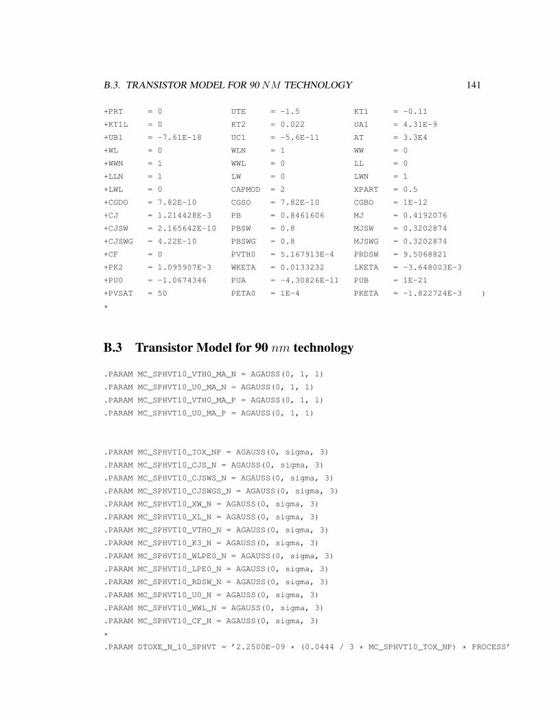
B.3. TRANSISTOR MODEL FOR 90 NM TECHNOLOGY 141
+PRT = 0 UTE = -1.5 KT1 = -0.11
+KT1L = 0 KT2 = 0.022 UA1 = 4.31E-9
+UB1 = -7.61E-18 UC1 = -5.6E-11 AT = 3.3E4
+WL = 0 WLN = 1 WW = 0
+WWN = 1 WWL = 0 LL = 0
+LLN = 1 LW = 0 LWN = 1
+LWL = 0 CAPMOD = 2 XPART = 0.5
+CGDO = 7.82E-10 CGSO = 7.82E-10 CGBO = 1E-12
+CJ = 1.214428E-3 PB = 0.8461606 MJ = 0.4192076
+CJSW = 2.165642E-10 PBSW = 0.8 MJSW = 0.3202874
+CJSWG = 4.22E-10 PBSWG = 0.8 MJSWG = 0.3202874
+CF = 0 PVTH0 = 5.167913E-4 PRDSW = 9.5068821
+PK2 = 1.095907E-3 WKETA = 0.0133232 LKETA = -3.648003E-3
+PU0 = -1.0674346 PUA = -4.30826E-11 PUB = 1E-21
+PVSAT = 50 PETA0 = 1E-4 PKETA = -1.822724E-3 )
*
B.3 Transistor Model for 90 nm technology
.PARAM MC_SPHVT10_VTH0_MA_N = AGAUSS(0, 1, 1)
.PARAM MC_SPHVT10_U0_MA_N = AGAUSS(0, 1, 1)
.PARAM MC_SPHVT10_VTH0_MA_P = AGAUSS(0, 1, 1)
.PARAM MC_SPHVT10_U0_MA_P = AGAUSS(0, 1, 1)
.PARAM MC_SPHVT10_TOX_NP = AGAUSS(0, sigma, 3)
.PARAM MC_SPHVT10_CJS_N = AGAUSS(0, sigma, 3)
.PARAM MC_SPHVT10_CJSWS_N = AGAUSS(0, sigma, 3)
.PARAM MC_SPHVT10_CJSWGS_N = AGAUSS(0, sigma, 3)
.PARAM MC_SPHVT10_XW_N = AGAUSS(0, sigma, 3)
.PARAM MC_SPHVT10_XL_N = AGAUSS(0, sigma, 3)
.PARAM MC_SPHVT10_VTH0_N = AGAUSS(0, sigma, 3)
.PARAM MC_SPHVT10_K3_N = AGAUSS(0, sigma, 3)
.PARAM MC_SPHVT10_WLPE0_N = AGAUSS(0, sigma, 3)
.PARAM MC_SPHVT10_LPE0_N = AGAUSS(0, sigma, 3)
.PARAM MC_SPHVT10_RDSW_N = AGAUSS(0, sigma, 3)
.PARAM MC_SPHVT10_U0_N = AGAUSS(0, sigma, 3)
.PARAM MC_SPHVT10_WWL_N = AGAUSS(0, sigma, 3)
.PARAM MC_SPHVT10_CF_N = AGAUSS(0, sigma, 3)
*
.PARAM DTOXE_N_10_SPHVT = ’2.2500E-09 * (0.0444 / 3 * MC_SPHVT10_TOX_NP) * PROCESS’
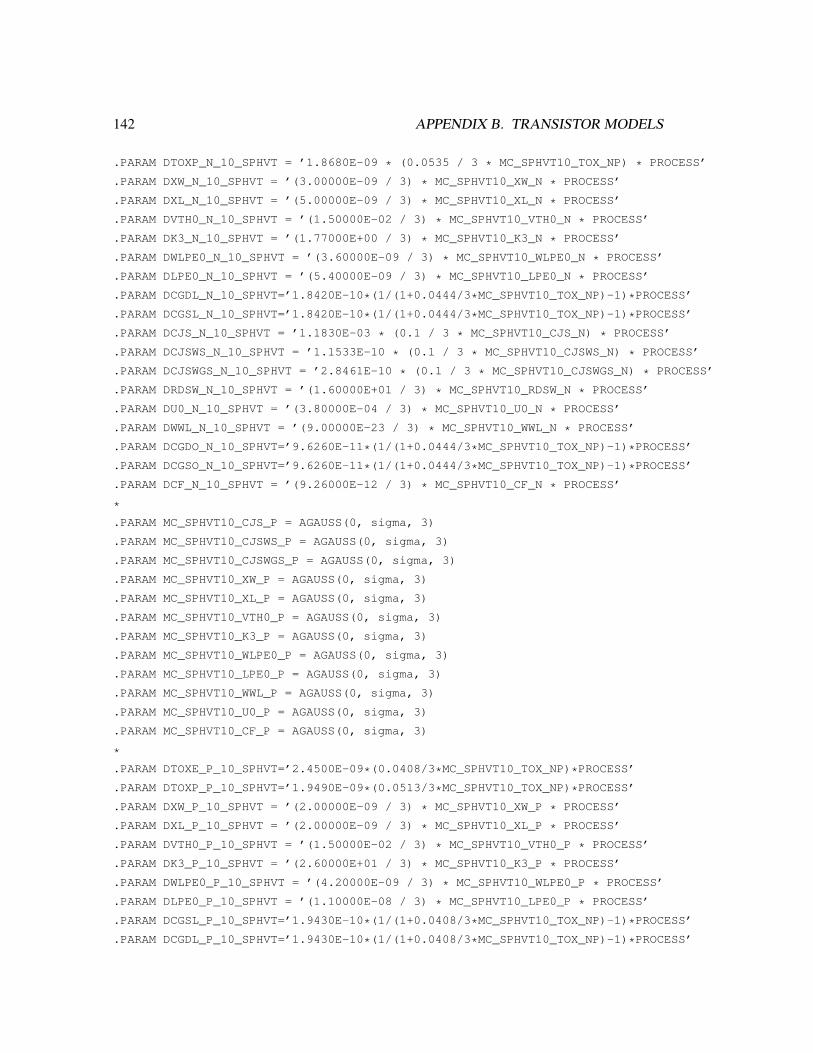
142 APPENDIX B. TRANSISTOR MODELS
.PARAM DTOXP_N_10_SPHVT = ’1.8680E-09 * (0.0535 / 3 * MC_SPHVT10_TOX_NP) * PROCESS’
.PARAM DXW_N_10_SPHVT = ’(3.00000E-09 / 3) * MC_SPHVT10_XW_N * PROCESS’
.PARAM DXL_N_10_SPHVT = ’(5.00000E-09 / 3) * MC_SPHVT10_XL_N * PROCESS’
.PARAM DVTH0_N_10_SPHVT = ’(1.50000E-02 / 3) * MC_SPHVT10_VTH0_N * PROCESS’
.PARAM DK3_N_10_SPHVT = ’(1.77000E+00 / 3) * MC_SPHVT10_K3_N * PROCESS’
.PARAM DWLPE0_N_10_SPHVT = ’(3.60000E-09 / 3) * MC_SPHVT10_WLPE0_N * PROCESS’
.PARAM DLPE0_N_10_SPHVT = ’(5.40000E-09 / 3) * MC_SPHVT10_LPE0_N * PROCESS’
.PARAM DCGDL_N_10_SPHVT=’1.8420E-10*(1/(1+0.0444/3*MC_SPHVT10_TOX_NP)-1)*PROCESS’
.PARAM DCGSL_N_10_SPHVT=’1.8420E-10*(1/(1+0.0444/3*MC_SPHVT10_TOX_NP)-1)*PROCESS’
.PARAM DCJS_N_10_SPHVT = ’1.1830E-03 * (0.1 / 3 * MC_SPHVT10_CJS_N) * PROCESS’
.PARAM DCJSWS_N_10_SPHVT = ’1.1533E-10 * (0.1 / 3 * MC_SPHVT10_CJSWS_N) * PROCESS’
.PARAM DCJSWGS_N_10_SPHVT = ’2.8461E-10 * (0.1 / 3 * MC_SPHVT10_CJSWGS_N) * PROCESS’
.PARAM DRDSW_N_10_SPHVT = ’(1.60000E+01 / 3) * MC_SPHVT10_RDSW_N * PROCESS’
.PARAM DU0_N_10_SPHVT = ’(3.80000E-04 / 3) * MC_SPHVT10_U0_N * PROCESS’
.PARAM DWWL_N_10_SPHVT = ’(9.00000E-23 / 3) * MC_SPHVT10_WWL_N * PROCESS’
.PARAM DCGDO_N_10_SPHVT=’9.6260E-11*(1/(1+0.0444/3*MC_SPHVT10_TOX_NP)-1)*PROCESS’
.PARAM DCGSO_N_10_SPHVT=’9.6260E-11*(1/(1+0.0444/3*MC_SPHVT10_TOX_NP)-1)*PROCESS’
.PARAM DCF_N_10_SPHVT = ’(9.26000E-12 / 3) * MC_SPHVT10_CF_N * PROCESS’
*
.PARAM MC_SPHVT10_CJS_P = AGAUSS(0, sigma, 3)
.PARAM MC_SPHVT10_CJSWS_P = AGAUSS(0, sigma, 3)
.PARAM MC_SPHVT10_CJSWGS_P = AGAUSS(0, sigma, 3)
.PARAM MC_SPHVT10_XW_P = AGAUSS(0, sigma, 3)
.PARAM MC_SPHVT10_XL_P = AGAUSS(0, sigma, 3)
.PARAM MC_SPHVT10_VTH0_P = AGAUSS(0, sigma, 3)
.PARAM MC_SPHVT10_K3_P = AGAUSS(0, sigma, 3)
.PARAM MC_SPHVT10_WLPE0_P = AGAUSS(0, sigma, 3)
.PARAM MC_SPHVT10_LPE0_P = AGAUSS(0, sigma, 3)
.PARAM MC_SPHVT10_WWL_P = AGAUSS(0, sigma, 3)
.PARAM MC_SPHVT10_U0_P = AGAUSS(0, sigma, 3)
.PARAM MC_SPHVT10_CF_P = AGAUSS(0, sigma, 3)
*
.PARAM DTOXE_P_10_SPHVT=’2.4500E-09*(0.0408/3*MC_SPHVT10_TOX_NP)*PROCESS’
.PARAM DTOXP_P_10_SPHVT=’1.9490E-09*(0.0513/3*MC_SPHVT10_TOX_NP)*PROCESS’
.PARAM DXW_P_10_SPHVT = ’(2.00000E-09 / 3) * MC_SPHVT10_XW_P * PROCESS’
.PARAM DXL_P_10_SPHVT = ’(2.00000E-09 / 3) * MC_SPHVT10_XL_P * PROCESS’
.PARAM DVTH0_P_10_SPHVT = ’(1.50000E-02 / 3) * MC_SPHVT10_VTH0_P * PROCESS’
.PARAM DK3_P_10_SPHVT = ’(2.60000E+01 / 3) * MC_SPHVT10_K3_P * PROCESS’
.PARAM DWLPE0_P_10_SPHVT = ’(4.20000E-09 / 3) * MC_SPHVT10_WLPE0_P * PROCESS’
.PARAM DLPE0_P_10_SPHVT = ’(1.10000E-08 / 3) * MC_SPHVT10_LPE0_P * PROCESS’
.PARAM DCGSL_P_10_SPHVT=’1.9430E-10*(1/(1+0.0408/3*MC_SPHVT10_TOX_NP)-1)*PROCESS’
.PARAM DCGDL_P_10_SPHVT=’1.9430E-10*(1/(1+0.0408/3*MC_SPHVT10_TOX_NP)-1)*PROCESS’
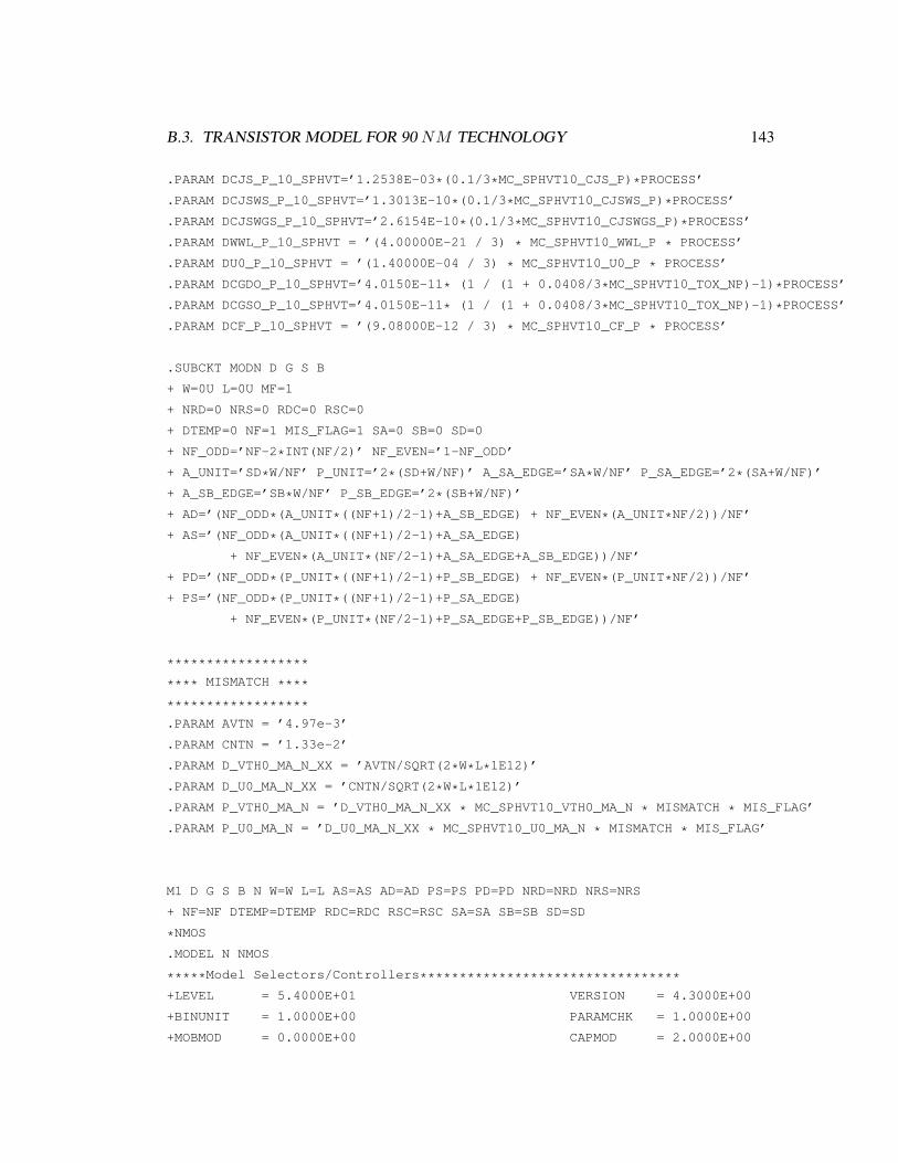
B.3. TRANSISTOR MODEL FOR 90 NM TECHNOLOGY 143
.PARAM DCJS_P_10_SPHVT=’1.2538E-03*(0.1/3*MC_SPHVT10_CJS_P)*PROCESS’
.PARAM DCJSWS_P_10_SPHVT=’1.3013E-10*(0.1/3*MC_SPHVT10_CJSWS_P)*PROCESS’
.PARAM DCJSWGS_P_10_SPHVT=’2.6154E-10*(0.1/3*MC_SPHVT10_CJSWGS_P)*PROCESS’
.PARAM DWWL_P_10_SPHVT = ’(4.00000E-21 / 3) * MC_SPHVT10_WWL_P * PROCESS’
.PARAM DU0_P_10_SPHVT = ’(1.40000E-04 / 3) * MC_SPHVT10_U0_P * PROCESS’
.PARAM DCGDO_P_10_SPHVT=’4.0150E-11* (1 / (1 + 0.0408/3*MC_SPHVT10_TOX_NP)-1)*PROCESS’
.PARAM DCGSO_P_10_SPHVT=’4.0150E-11* (1 / (1 + 0.0408/3*MC_SPHVT10_TOX_NP)-1)*PROCESS’
.PARAM DCF_P_10_SPHVT = ’(9.08000E-12 / 3) * MC_SPHVT10_CF_P * PROCESS’
.SUBCKT MODN D G S B
+ W=0U L=0U MF=1
+ NRD=0 NRS=0 RDC=0 RSC=0
+ DTEMP=0 NF=1 MIS_FLAG=1 SA=0 SB=0 SD=0
+ NF_ODD=’NF-2*INT(NF/2)’ NF_EVEN=’1-NF_ODD’
+ A_UNIT=’SD*W/NF’ P_UNIT=’2*(SD+W/NF)’ A_SA_EDGE=’SA*W/NF’ P_SA_EDGE=’2*(SA+W/NF)’
+ A_SB_EDGE=’SB*W/NF’ P_SB_EDGE=’2*(SB+W/NF)’
+ AD=’(NF_ODD*(A_UNIT*((NF+1)/2-1)+A_SB_EDGE) + NF_EVEN*(A_UNIT*NF/2))/NF’
+ AS=’(NF_ODD*(A_UNIT*((NF+1)/2-1)+A_SA_EDGE)
+ NF_EVEN*(A_UNIT*(NF/2-1)+A_SA_EDGE+A_SB_EDGE))/NF’
+ PD=’(NF_ODD*(P_UNIT*((NF+1)/2-1)+P_SB_EDGE) + NF_EVEN*(P_UNIT*NF/2))/NF’
+ PS=’(NF_ODD*(P_UNIT*((NF+1)/2-1)+P_SA_EDGE)
+ NF_EVEN*(P_UNIT*(NF/2-1)+P_SA_EDGE+P_SB_EDGE))/NF’
******************
**** MISMATCH ****
******************
.PARAM AVTN = ’4.97e-3’
.PARAM CNTN = ’1.33e-2’
.PARAM D_VTH0_MA_N_XX = ’AVTN/SQRT(2*W*L*1E12)’
.PARAM D_U0_MA_N_XX = ’CNTN/SQRT(2*W*L*1E12)’
.PARAM P_VTH0_MA_N = ’D_VTH0_MA_N_XX * MC_SPHVT10_VTH0_MA_N * MISMATCH * MIS_FLAG’
.PARAM P_U0_MA_N = ’D_U0_MA_N_XX * MC_SPHVT10_U0_MA_N * MISMATCH * MIS_FLAG’
M1 D G S B N W=W L=L AS=AS AD=AD PS=PS PD=PD NRD=NRD NRS=NRS
+ NF=NF DTEMP=DTEMP RDC=RDC RSC=RSC SA=SA SB=SB SD=SD
*NMOS
.MODEL N NMOS
*****Model Selectors/Controllers*********************************
+LEVEL = 5.4000E+01 VERSION = 4.3000E+00
+BINUNIT = 1.0000E+00 PARAMCHK = 1.0000E+00
+MOBMOD = 0.0000E+00 CAPMOD = 2.0000E+00
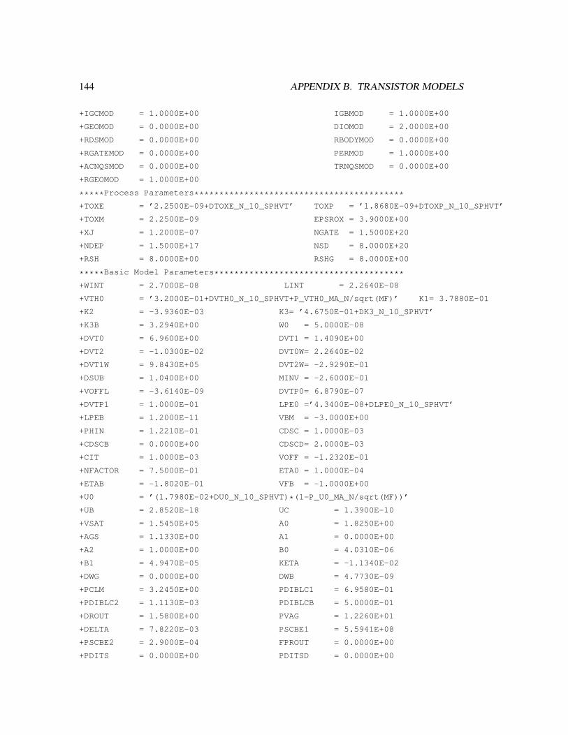
144 APPENDIX B. TRANSISTOR MODELS
+IGCMOD = 1.0000E+00 IGBMOD = 1.0000E+00
+GEOMOD = 0.0000E+00 DIOMOD = 2.0000E+00
+RDSMOD = 0.0000E+00 RBODYMOD = 0.0000E+00
+RGATEMOD = 0.0000E+00 PERMOD = 1.0000E+00
+ACNQSMOD = 0.0000E+00 TRNQSMOD = 0.0000E+00
+RGEOMOD = 1.0000E+00
*****Process Parameters******************************************
+TOXE = ’2.2500E-09+DTOXE_N_10_SPHVT’ TOXP = ’1.8680E-09+DTOXP_N_10_SPHVT’
+TOXM = 2.2500E-09 EPSROX = 3.9000E+00
+XJ = 1.2000E-07 NGATE = 1.5000E+20
+NDEP = 1.5000E+17 NSD = 8.0000E+20
+RSH = 8.0000E+00 RSHG = 8.0000E+00
*****Basic Model Parameters**************************************
+WINT = 2.7000E-08 LINT = 2.2640E-08
+VTH0 = ’3.2000E-01+DVTH0_N_10_SPHVT+P_VTH0_MA_N/sqrt(MF)’ K1= 3.7880E-01
+K2 = -3.9360E-03 K3= ’4.6750E-01+DK3_N_10_SPHVT’
+K3B = 3.2940E+00 W0 = 5.0000E-08
+DVT0 = 6.9600E+00 DVT1 = 1.4090E+00
+DVT2 = -1.0300E-02 DVT0W= 2.2640E-02
+DVT1W = 9.8430E+05 DVT2W= -2.9290E-01
+DSUB = 1.0400E+00 MINV = -2.6000E-01
+VOFFL = -3.6140E-09 DVTP0= 6.8790E-07
+DVTP1 = 1.0000E-01 LPE0 =’4.3400E-08+DLPE0_N_10_SPHVT’
+LPEB = 1.2000E-11 VBM = -3.0000E+00
+PHIN = 1.2210E-01 CDSC = 1.0000E-03
+CDSCB = 0.0000E+00 CDSCD= 2.0000E-03
+CIT = 1.0000E-03 VOFF = -1.2320E-01
+NFACTOR = 7.5000E-01 ETA0 = 1.0000E-04
+ETAB = -1.8020E-01 VFB = -1.0000E+00
+U0 = ’(1.7980E-02+DU0_N_10_SPHVT)*(1-P_U0_MA_N/sqrt(MF))’
+UB = 2.8520E-18 UC = 1.3900E-10
+VSAT = 1.5450E+05 A0 = 1.8250E+00
+AGS = 1.1330E+00 A1 = 0.0000E+00
+A2 = 1.0000E+00 B0 = 4.0310E-06
+B1 = 4.9470E-05 KETA = -1.1340E-02
+DWG = 0.0000E+00 DWB = 4.7730E-09
+PCLM = 3.2450E+00 PDIBLC1 = 6.9580E-01
+PDIBLC2 = 1.1130E-03 PDIBLCB = 5.0000E-01
+DROUT = 1.5800E+00 PVAG = 1.2260E+01
+DELTA = 7.8220E-03 PSCBE1 = 5.5941E+08
+PSCBE2 = 2.9000E-04 FPROUT = 0.0000E+00
+PDITS = 0.0000E+00 PDITSD = 0.0000E+00

B.3. TRANSISTOR MODEL FOR 90 NM TECHNOLOGY 145
+PDITSL = 1.0000E-10 UA = -1.9120E-09
*****Parameters for Asymmetric and Bias-Dependent Rds Model******
+RDSW = ’7.9800E+01+DRDSW_N_10_SPHVT’ RDSWMIN = 6.3000E+01
+PRWG = 3.2000E-02 PRWB = 1.4250E-01
+WR = 1.0000E+00
*****Impact Ionization Current Model Parameters******************
+ALPHA0 = 5.7860E-04 ALPHA1 = 0.0000E+00
+BETA0 = 2.2510E+01
*****Gate-Induced Drain Leakage Model Parameters*****************
+AGIDL = 2.8460E-08 BGIDL = 1.5390E+09
+CGIDL = 3.7557E+00 EGIDL = 7.3920E-01
*****Gate Dielectric Tunneling Current Model Parameters**********
+TOXREF = 2.2500E-09 DLCIG = 2.0350E-08
+AIGBACC = 1.1689E-02 BIGBACC = 3.7530E-03
+CIGBACC = 2.2315E-01 NIGBACC = 5.0000E+00
+AIGBINV = 2.0550E-02 BIGBINV = 6.2780E-03
+CIGBINV = 1.6980E-03 EIGBINV = 6.6490E-01
+NIGBINV = 1.5090E+04 AIGC = 1.0860E-02
+BIGC = 1.8970E-03 CIGC = 3.3220E-02
+AIGSD = 1.0100E-02 BIGSD = 3.2410E-04
+CIGSD = 5.6600E-03 NIGC = 5.0000E-01
+POXEDGE = 1.0200E+00 PIGCD = 1.0000E+00
+NTOX = 1.0000E+00 LBIGSD = 7.4750E-06
*****Charge and Capacitance Model Parameters*********************
+DLC = 1.6870E-08 DWC = -3.0000E-08
+XPART = 1.0000E+00 CGSO =’9.6260E-11+DCGSO_N_10_SPHVT’
+CGDO = ’9.6260E-11+DCGDO_N_10_SPHVT’ CGBO = 0.0000E+00
+CGDL = ’1.8420E-10+DCGDL_N_10_SPHVT’ CGSL =’1.8420E-10+DCGSL_N_10_SPHVT’
+CLC = 7.6330E-08 CLE = 7.0000E-01
+CF = ’9.2600E-11+DCF_N_10_SPHVT’ CKAPPAS = 1.0000E+00
+CKAPPAD = 1.0000E+00 VFBCV = 0.0000E+00
+ACDE = 2.2170E-01 MOIN = 7.8990E+00
+NOFF = 2.3840E+00 VOFFCV = -7.9880E-02
*****High-Speed/RF Model Parameters******************************
*****Flicker and Thermal Noise Model Parameters******************
+FNOIMOD = 1.0000E+00 TNOIMOD = 0.0000E+00
+EF = 1.0494E+00 NOIA = 8.4300E+41
+NOIB = 1.8600E+23 NOIC = 2.8700E+09
+EM = 6.3600E+06 NTNOI = 1.0000E+00
*****Layout-Dependent Parasitics Model Parameters****************
+XL = ’-1.0000E-08+DXL_N_10_SPHVT’ XW =’-0.0000E-00+DXW_N_10_SPHVT’
+DMCG = 1.6000E-07 DMCI= 1.0000E-07
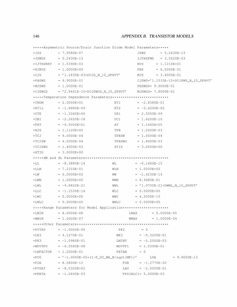
146 APPENDIX B. TRANSISTOR MODELS
*****Asymmetric Source/Drain Junction Diode Model Parameters*****
+JSS = 7.9580E-07 JSWS = 5.2430E-13
+JSWGS = 5.2430E-13 IJTHSFWD = 3.5620E-03
+IJTHSREV = 1.5390E-03 BVS = 1.1210E+01
+XJBVS = 1.0000E+00 PBS = 6.5000E-01
+CJS = ’1.1830E-03+DCJS_N_10_SPHVT’ MJS = 3.4000E-01
+PBSWS = 9.9000E-01 CJSWS=’1.1533E-10+DCJSWS_N_10_SPHVT’
+MJSWS = 1.0000E-01 PBSWGS= 9.9000E-01
+CJSWGS = ’2.8461E-10+DCJSWGS_N_10_SPHVT’ MJSWGS= 7.8000E-01
*****Temperature Dependence Parameters***************************
+TNOM = 2.5000E+01 KT1 = -2.8580E-01
+KT1L = -1.8880E-09 KT2 = -3.4200E-02
+UTE = -1.3340E+00 UA1 = 2.5050E-09
+UB1 = -2.2650E-18 UC1 = 1.6200E-10
+PRT = -4.5000E+01 AT = 1.1660E+05
+NJS = 1.1120E+00 TPB = 1.2000E-03
+TCJ = 9.0000E-04 TPBSW = 1.0000E-04
+TCJSW = 4.0000E-04 TPBSWG = 1.8000E-03
+TCJSWG = 1.4000E-03 XTIS = 3.0000E+00
+XTID = 3.0000E+00
*****dW and dL Parameters****************************************
+LL = -8.3880E-14 WL = -6.1460E-15
+LLN = 7.2310E-01 WLN = 1.0000E+00
+LW = 0.0000E+00 WW = -1.4230E-14
+LWN = 1.0000E+00 WWN = 8.9480E-01
+LWL = -9.8820E-21 WWL = ’1.9700E-21+DWWL_N_10_SPHVT’
+LLC = -1.1530E-14 WLC = 0.0000E+00
+LWC = 0.0000E+00 WWC = 4.5000E-15
+LWLC = 0.0000E+00 WWLC = 0.0000E+00
*****Range Parameters for Model Application**********************
+LMIN = 8.0000E-08 LMAX = 5.0000E-05
+WMIN = 1.2000E-07 WMAX = 1.0000E-04
*****Other Parameters********************************************
+PVTH0 = -1.0000E-05 PK2 = 0
+LK3 = 4.1270E-01 WK3 = -5.3200E-01
+PK3 = -1.0980E-01 LMINV = -5.2000E-03
+WDVTP0 = -6.0580E-08 WDVTP1 = 1.0390E-01
+LNFACTOR = 1.2000E-01 PETAB = 0
+PU0 = ’-1.0000E-05*(1-P_U0_MA_N/sqrt(MF))’ LUA = 9.9000E-13
+PUA = 8.5800E-12 PUB = -1.2770E-20
+PVSAT = -8.5320E+02 LA0 = -2.0000E-01
+PKETA = -1.0660E-03 PPDIBLC1= 5.0000E-03
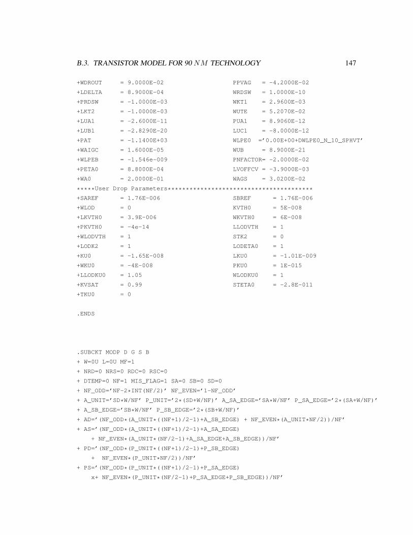
B.3. TRANSISTOR MODEL FOR 90 NM TECHNOLOGY 147
+WDROUT = 9.0000E-02 PPVAG = -4.2000E-02
+LDELTA = 8.9000E-04 WRDSW = 1.0000E-10
+PRDSW = -1.0000E-03 WKT1 = 2.9600E-03
+LKT2 = -1.0000E-03 WUTE = 5.2070E-02
+LUA1 = -2.6000E-11 PUA1 = 8.9060E-12
+LUB1 = -2.8290E-20 LUC1 = -8.0000E-12
+PAT = -1.1400E+03 WLPE0 =’0.00E+00+DWLPE0_N_10_SPHVT’
+WAIGC = 1.6000E-05 WUB = 8.9000E-21
+WLPEB = -1.546e-009 PNFACTOR= -2.0000E-02
+PETA0 = 8.8000E-04 LVOFFCV = -3.9000E-03
+WA0 = 2.0000E-01 WAGS = 3.0200E-02
*****User Drop Parameters****************************************
+SAREF = 1.76E-006 SBREF = 1.76E-006
+WLOD = 0 KVTH0 = 5E-008
+LKVTH0 = 3.9E-006 WKVTH0 = 6E-008
+PKVTH0 = -4e-14 LLODVTH = 1
+WLODVTH = 1 STK2 = 0
+LODK2 = 1 LODETA0 = 1
+KU0 = -1.65E-008 LKU0 = -1.01E-009
+WKU0 = -4E-008 PKU0 = 1E-015
+LLODKU0 = 1.05 WLODKU0 = 1
+KVSAT = 0.99 STETA0 = -2.8E-011
+TKU0 = 0
.ENDS
.SUBCKT MODP D G S B
+ W=0U L=0U MF=1
+ NRD=0 NRS=0 RDC=0 RSC=0
+ DTEMP=0 NF=1 MIS_FLAG=1 SA=0 SB=0 SD=0
+ NF_ODD=’NF-2*INT(NF/2)’ NF_EVEN=’1-NF_ODD’
+ A_UNIT=’SD*W/NF’ P_UNIT=’2*(SD+W/NF)’ A_SA_EDGE=’SA*W/NF’ P_SA_EDGE=’2*(SA+W/NF)’
+ A_SB_EDGE=’SB*W/NF’ P_SB_EDGE=’2*(SB+W/NF)’
+ AD=’(NF_ODD*(A_UNIT*((NF+1)/2-1)+A_SB_EDGE) + NF_EVEN*(A_UNIT*NF/2))/NF’
+ AS=’(NF_ODD*(A_UNIT*((NF+1)/2-1)+A_SA_EDGE)
+ NF_EVEN*(A_UNIT*(NF/2-1)+A_SA_EDGE+A_SB_EDGE))/NF’
+ PD=’(NF_ODD*(P_UNIT*((NF+1)/2-1)+P_SB_EDGE)
+ NF_EVEN*(P_UNIT*NF/2))/NF’
+ PS=’(NF_ODD*(P_UNIT*((NF+1)/2-1)+P_SA_EDGE)
x+ NF_EVEN*(P_UNIT*(NF/2-1)+P_SA_EDGE+P_SB_EDGE))/NF’

148 APPENDIX B. TRANSISTOR MODELS
******************
**** MISMATCH ****
******************
.PARAM AVTP = ’3.32e-3’
.PARAM CNTP = ’1.18e-2’
.PARAM D_VTH0_MA_P_XX = ’AVTP/SQRT(2*W*L*1E12)’
.PARAM D_U0_MA_P_XX = ’CNTP/SQRT(2*W*L*1E12)’
.PARAM P_VTH0_MA_P = ’D_VTH0_MA_P_XX * MC_SPHVT10_VTH0_MA_P * MISMATCH * MIS_FLAG’
.PARAM P_U0_MA_P = ’D_U0_MA_P_XX * MC_SPHVT10_U0_MA_P * MISMATCH * MIS_FLAG’
M1 D G S B P W=W L=L AS=AS AD=AD PS=PS PD=PD NRD=NRD NRS=NRS
+ NF=NF DTEMP=DTEMP RDC=RDC RSC=RSC SA=SA SB=SB SD=SD
.MODEL P PMOS
*****Model Selectors/Controllers*********************************
+LEVEL = 5.4000E+01 VERSION = 4.3000E+00
+BINUNIT = 1.0000E+00 PARAMCHK = 1.0000E+00
+MOBMOD = 0.0000E+00 CAPMOD = 2.0000E+00
+IGCMOD = 1.0000E+00 IGBMOD = 1.0000E+00
+GEOMOD = 0.0000E+00 DIOMOD = 2.0000E+00
+RDSMOD = 0.0000E+00 RBODYMOD = 0.0000E+00
+RGATEMOD = 0.0000E+00 PERMOD = 1.0000E+00
+ACNQSMOD = 0.0000E+00 TRNQSMOD = 0.0000E+00
+RGEOMOD = 1.0000E+00
*****Process Parameters******************************************
+TOXE = ’2.4500E-09+DTOXE_P_10_SPHVT’ TOXP=’1.9490E-09+DTOXP_P_10_SPHVT’
+TOXM = 2.4500E-09 EPSROX= 3.9000E+00
+XJ = 1.2000E-07 NGATE = 1.0000E+20
+NDEP = 3.0000E+17 NSD = 6.0000E+20
+RSH = 8.0000E+00 RSHG = 8.0000E+00
*****Basic Model Parameters**************************************
+WINT = 5.2200E-08 LINT = -1.2150E-08
+VTH0 = ’-2.7300E-01+DVTH0_P_10_SPHVT+P_VTH0_MA_P/sqrt(MF)’ K1=3.2640E-01
+K2 = -3.7280E-02 K3 = ’-8.6360E+00+DK3_P_10_SPHVT’
+K3B = 2.0610E+01 W0 = 2.6180E-06
+DVT0 = 7.0830E-03 DVT1 = 2.5060E-01
+DVT2 = -1.3800E-01 DVT0W = 7.6250E-04
+DVT1W = 4.2100E+05 DVT2W = 1.0000E-02
+DSUB = 6.9620E-01 MINV = 1.5000E-01
+VOFFL = -2.4850E-09 DVTP0 = 2.4730E-07
+DVTP1 = 7.8000E-01 LPE0 = ’0.7100E-08+DLPE0_P_10_SPHVT’

B.3. TRANSISTOR MODEL FOR 90 NM TECHNOLOGY 149
+LPEB = 5.8520E-08 VBM = -3.0000E+00
+PHIN = 1.1420E-01 CDSC = 1.0000E-03
+CDSCB = 0.0000E+00 CDSCD = 0.0000E+00
+CIT = 0.0000E+00 VOFF = -1.0540E-01
+NFACTOR = 7.5650E-01 ETA0 = 3.9980E-01
+ETAB = -3.5190E-01 VFB = -1.0000E+00
+U0 = ’(7.2600E-03+DU0_P_10_SPHVT)*(1-P_U0_MA_P/sqrt(MF))’
+UB = 1.0900E-18 UC = -1.5950E-11
+VSAT = 1.5620E+05 A0 = 2.3520E+00
+AGS = 1.0850E+00 A1 = 0.0000E+00
+A2 = 3.5000E-01 B0 = 6.5600E-07
+B1 = 4.9610E-05 KETA = -6.5400E-02
+DWG = -2.6510E-08 DWB = -5.8000E-09
+PCLM = 3.5490E-01 PDIBLC1 = 1.0000E-07
+PDIBLC2 = 1.2320E-03 PDIBLCB = -4.8600E-01
+DROUT = 5.1190E-01 PVAG = 0.0000E+00
+DELTA = 9.9470E-03 PSCBE1 = 1.5350E+09
+PSCBE2 = 1.1467E-07 FPROUT = 2.7610E+02
+PDITS = 5.0000E-07 PDITSD = 0.0000E+00
+PDITSL = 0.0000E+00 UA = 4.5580E-11
*****Parameters for Asymmetric and Bias-Dependent Rds Model******
+RDSW = 1.1800E+02 RDSWMIN = 1.0150E+02
+PRWG = 0.0000E+00 PRWB = -8.0000E-02
+WR = 1.0000E+00
*****Impact Ionization Current Model Parameters******************
+ALPHA0 = 3.0000E-08 ALPHA1 = 0.0000E+00
+BETA0 = 2.1700E+01
*****Gate-Induced Drain Leakage Model Parameters*****************
+AGIDL = 4.2700E-10 BGIDL = 1.4510E+09
+CGIDL = 1.1080E+00 EGIDL = 6.4550E-01
*****Gate Dielectric Tunneling Current Model Parameters**********
+TOXREF = 2.4500E-09 DLCIG = 1.8000E-08
+AIGBACC = 1.0360E-02 BIGBACC = 8.1090E-03
+CIGBACC = 9.1080E-01 NIGBACC = 4.3790E+00
+AIGBINV = 1.6100E-02 BIGBINV = 6.2290E-03
+CIGBINV = 1.0950E-01 EIGBINV = 9.6280E-02
+NIGBINV = 3.0500E+00 AIGC = 5.9290E-03
+BIGC = 5.1880E-04 CIGC = 5.8650E-02
+AIGSD = 5.9900E-03 BIGSD = 9.9050E-05
+CIGSD = 3.4690E-06 NIGC = 1.3800E+00
+POXEDGE = 1.0000E+00 PIGCD = 1.0000E+00
+NTOX = 1.0000E+00
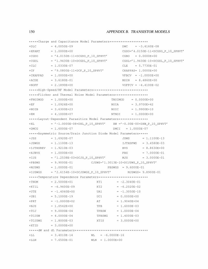
150 APPENDIX B. TRANSISTOR MODELS
*****Charge and Capacitance Model Parameters*********************
+DLC = 4.0050E-09 DWC = -3.4160E-08
+XPART = 1.0000E+00 CGSO=’4.0150E-11+DCGSO_P_10_SPHVT’
+CGDO = ’4.0150E-11+DCGDO_P_10_SPHVT’ CGBO = 0.0000E+00
+CGDL = ’1.9430E-10+DCGDL_P_10_SPHVT’ CGSL=’1.9430E-10+DCGSL_P_10_SPHVT’
+CLC = 1.0330E-07 CLE = 5.7730E-01
+CF = ’9.0800E-11+DCF_P_10_SPHVT’ CKAPPAS= 1.0000E+00
+CKAPPAD = 1.0000E+00 VFBCV = -1.0000E+00
+ACDE = 3.6180E-01 MOIN = 8.4860E+00
+NOFF = 2.1890E+00 VOFFCV = -4.4100E-02
*****High-Speed/RF Model Parameters******************************
*****Flicker and Thermal Noise Model Parameters******************
+FNOIMOD = 1.0000E+00 TNOIMOD = 0.0000E+00
+EF = 1.0926E+00 NOIA = 3.9700E+42
+NOIB = 3.6300E+23 NOIC = 1.9900E+10
+EM = 4.1000E+07 NTNOI = 1.0000E+00
*****Layout-Dependent Parasitics Model Parameters****************
+XL = ’-1.0000E-08+DXL_P_10_SPHVT’ XW =’-0.00E-00+DXW_P_10_SPHVT’
+DMCG = 1.6000E-07 DMCI = 1.0000E-07
*****Asymmetric Source/Drain Junction Diode Model Parameters*****
+JSS = 1.6920E-07 JSWS = 1.1100E-13
+JSWGS = 1.1100E-13 IJTHSFWD = 3.4580E-03
+IJTHSREV = 1.9210E-03 BVS = 8.8630E+00
+XJBVS = 1.0000E+00 PBS = 7.0000E-01
+CJS = ’1.2538E-03+DCJS_P_10_SPHVT’ MJS = 3.0000E-01
+PBSWS = 9.9000E-01 CJSWS=’1.3013E-10+DCJSWS_P_10_SPHVT’
+MJSWS = 1.0000E-01 PBSWGS = 9.6000E-01
+CJSWGS = ’2.6154E-10+DCJSWGS_P_10_SPHVT’ MJSWGS= 9.8900E-01
*****Temperature Dependence Parameters***************************
+TNOM = 2.5000E+01 KT1 = -2.3040E-01
+KT1L = -6.9600E-09 KT2 = -6.2020E-02
+UTE = -1.4060E+00 UA1 = -1.3050E-10
+UB1 = 5.1000E-19 UC1 = 0.0000E+00
+PRT = -1.0000E+02 AT = 1.9040E+04
+NJS = 1.0542E+00 TPB = 1.6000E-03
+TCJ = 9.0000E-04 TPBSW = 1.0000E-04
+TCJSW = 4.0000E-04 TPBSWG = 1.4000E-03
+TCJSWG = 1.8000E-03 XTIS = 3.0000E+00
+XTID = 3.0000E+00
*****dW and dL Parameters****************************************
+LL = 3.4010E-14 WL = -6.0000E-16
+LLN = 7.6500E-01 WLN = 1.0000E+00

B.3. TRANSISTOR MODEL FOR 90 NM TECHNOLOGY 151
+LW = -4.0000E-15 WW = -1.2840E-12
+LWN = 1.0000E+00 WWN = 6.7930E-01
+LWL = 0.0000E+00 WWL = ’-1.1530E-20+DWWL_P_10_SPHVT’
+LLC = 3.3010E-14 WLC = 0.0000E+00
+LWC = 0.0000E+00 WWC = 2.0000E-13
+LWLC = 0.0000E+00 WWLC = 0.0000E+00
*****Range Parameters for Model Application**********************
+LMIN = 8.0000E-08 LMAX = 5.0000E-05
+WMIN = 1.2000E-07 WMAX = 1.0000E-04
*****Other Parameters********************************************
+PVTH0 = -1.7080E-03 WK3 = -6.9340E+00
+WK3B = 5.3770E+00 PK3B = -3.1550E-01
+LDVT0 = 3.7540E-02 PDSUB = -3.6680E-03
+LLPE0 = 4.6200E-09 WLPE0 = ’-8.4620E-09+DWLPE0_P_10_SPHVT’
+WLPEB = -1.0720E-08 WVOFF = 7.6650E-04
+LNFACTOR = 3.9000E-02 WNFACTOR= -1.0650E-01
+WUA = -5.8690E-11 WUB = 1.2300E-19
+PUB = -5.3250E-21 PVSAT = -1.7380E+03
+LA0 = 1.2610E-01 LAGS = 5.0000E-01
+LKETA = 4.4490E-03 WKETA = 8.8800E-03
+PPCLM = 6.7610E-03 LDELTA = 9.0000E-04
+PRDSW = 1.0200E-01 WKT1 = 2.0000E-03
+LKT2 = 1.9700E-03 WUTE = -2.8000E-02
+WUA1 = -3.8400E-11 LUB1 = -5.0600E-20
+WUC1 = 4.3440E-11 PETAB = 0.01
+LVOFFCV = -4.0000E-03 WAIGSD = 3.3000E-05
+PAIGSD = 4.5000E-06 PNFACTOR= 1.8000E-02
+SAREF = 1.76E-006 SBREF = 1.76E-006
+WLOD = 0 KVTH0 = -8E-10
+LKVTH0 = -1.5e-6 WKVTH0 = 6e-7
+PKVTH0 = 0 LLODVTH = 0.8
+WLODVTH = 1 STK2 = 0
+LODK2 = 1 LODETA0 = 1
+KU0 = 5.3E-007 LKU0 = 5.8E-004
+WKU0 = -1.10E-9 PKU0 = -2.5E-010
+LLODKU0 = 0.68 WLODKU0 = 0.85
+KVSAT = 1 STETA0 = 3.8E-010
+TKU0 = 0
.ENDS

152 APPENDIX B. TRANSISTOR MODELS

Bibliography
[1] F. Medeiro, F.V. Fernandez, R. Domınguez-Castro, and A. Rodrıguez-Vazquez. A Statistical Optimization-
based Approach For Automated Sizing Of Analog Cells. International Conference on Computer-Aided De-
sign, pages 594 – 597, 1994.
[2] John R. Koza, Lee W. Jones, Martin A. Keane, Matthew J. Streeter, and Sameer H. Al-Sakran. Genetic Pro-
gramming Theory and Practice II, chapter Toward Automated Design Of Industrial-Strength Analog Circuits
By Means Of Genetic Programming. Springer, 2005.
[3] Georges Gielen and Wim Dehaene. Analog and digital circuit design in 65 nm CMOS: end of the road?
Design, Automation and Test in Europe, pages 37–42, 2005.
[4] Georges Gielen, Tom Eeckelaert, Ewout Martens, and Trent McConaghy. Automated synthesis of complex
analog circuits. European Conference on Circuit Theory and Design, 27(30):20–23, August 2007.
[5] Guo Yu and Peng Li. Yield-Aware Analog Integrated Circuit Optimization Using Geostatistics Motivated
Performance Modeling. IEEE/ACM International Conference on Computer-Aided Design, pages 464–469,
November 2007. San Jose, C.A.
[6] G. Yu and Peng Li. Yield-Aware Hierarchical Optimization of Large Analog Integrated Circuits. IEEE/ACM
International Conference on Computer-Aided Design, pages 79 – 84, November 2008.
[7] Tom Eeckelaert, Raf Schoofs, Georges Gielen, Michiel Steyaert, and Willy Sansen. Hierarchical Bottom-up
Analog Optimization Methodology Validated by a Delta-Sigma A/D Converter Design for the 802.11 a/b/g
Standard. Design Automation Conference, pages 25 – 30, July 2006.
[8] T. Eeckelaert, T. McConaghy, and G. Gielen. Efficient multiobjective synthesis of analog circuits using
hierarchical pareto optimal performance hypersurfaces. Design, Automation and Test in Europe, 2:1070 –
1075, March 2005.
[9] M. Buhler, J. Koehl, J. Bickford, J. Hibbeler, U. Schlichtmann, R. Sommer, M. Pronath, and A. Ripp.
DFM/DFY Design for Manufacturability and Yield - influence of process variations in digital, analog and
mixed-signal circuit design. Design, Automation, and Test in Europe, pages 387–392, 2006. Munich, Ger-
many.
[10] Esteban Tlelo-Cuautle, Ivick Guerra-Gomez, Carlos Alberto Reyes-Garcıa, and Miguel Aurelio Duarte-
Villasenor. Intelligent Systems for Automated Learning and Adaptation: Emerging Trends and Applications,
chapter 8: Synthesis of Analog Circuits by Genetic Algorithms and their Optimization by Particle Swarm
Optimization, pages 173–192. IGI Global, 2009.
153
154 BIBLIOGRAPHY
[11] Yann Cooren, Mourad Fakhfakh, Mourad Loulou, and Patrick Siarry. Optimizing Second Generation Current
Conveyors using Particle Swarm Optimization. Internatonal Conference on Microelectronics, pages 365–
368, December 2007. Cairo.
[12] Jernej Olensek, Arpad Burmen, Janez Puhan, and Tadej Tuma. DESA: a new hybrid global optimization
method and its application to analog integrated circuit sizing. Journal of Global Optimization, 44(1):53–77,
May 2009.
[13] Bo Liu, Yan Wang, Zhiping Yu, Leibo Liu, Miao Li, Zheng Wang, Jing Lu, and Francisco V. Fernndez. Ana-
log Circuit Optimization System Based on Hybrid Evolutionary Algorithms. Integration, the VLSI Journal,
42(2):137–148, February 2009.
[14] Ivick Guerra-Gomez, Esteban Tlelo-Cuautle, Trent McConaghy, and Geroges Gielen. Decomposition-Based
Multi-Objective Optimization of Second-Generation Current Conveyors. IEEE International Midwest Sym-
posium on Circuits and Systems, pages 220–223, August 2009.
[15] Anthony Scanlan. Application of Genetic Algorithms to Analogue Circuit Synthesis. Irish Signals and
Systems Conference, pages 339–344, June 2006. Dublin.
[16] Raf Schoofs, Tom Eeckelaert, Michiel Steyaert, Goerges Gielen, and Willy Sansen. A Continuous-Time
Delta-Sigma Modulator for 802.11a/b/g WLAN Implemented with a Hierarchical Bottom-up Optimization
Methodology. IEEE International Conference on Electronics, Circuits and Systems, 10(13):950 – 953, De-
cember 2006.
[17] Tom Eeckelaert, Raf Schoofs, Georges Gielen, Michiel Steyaert, and Willy Sansen. An Efficient Method-
ology for Hierarchical Synthesis of Mixed-Signal Systems with Fully Integrated Building Block Topology
Selection. Design, Automation and Test in Europe Conference and Exhibition, pages 1 – 6, April 2007.
[18] Henry Chang, Alberto Snagiovanni-Vincentelli, Felice Balarin, Edoardo Charbon, Umakanta Choudhury,
Gani Jusuf, Liu Edward, Enrico Malavasi, Robert Neff, and Paul R. Gray. A Top-Down, Constraint-Driven
Design Methodology for Analog Integrated Circuits. Proceedings of the IEEE Custom Integrated Circuits
Conference, pages 8.4.1 – 8.4.6, 1992.
[19] Geroges Gielen, Trent McConaghy, and Tom Eeckelaert. Performance Space Modeling for Hierarchical Syn-
thesis of Analog Integrated Circuits. Design Automation Conference, pages 881–886, June 2005. Anaheim,
Califomia, USA.
[20] Saurabh K Tiwary, Pragati K Tiwary, and Rob A Rutenbar. Generation of Yield-Aware Pareto Surfaces for
Hierarchical Circuit Design Space Exploration. Design Automation Conference, pages 31–36, July 2006. San
Francisco, California, USA.
[21] Rob A. Rutenbar. Design Automation for Analog: The Next Generation of Tool Challenges. IEEE/ACM
International Conference on Computer-Aided Design, 5(9):458 – 460, November 2006.
[22] Trent McConaghy, Pieter Palmers, Georges Gielen, and Michiel Steyaert. Automated extraction of expert
knowledge in analog topology selection and sizing. International Conference on Computer-Aided Design,
pages 392–395, November 2008. San Jose, CA.
[23] Ewout Martens and Georges Gielen. Classification of analog synthesis tools based on their architecture
selection mechanisms. INTEGRATION, the VLSI journal, 41:238–252, February 2008.
BIBLIOGRAPHY 155
[24] T. McConaghy and G. Gielen. CAFFEINE: template-free symbolic model generation of analog circuits via
canonical form functions and genetic programming. Transactions on Computer-Aided Design of Integrated
Circuits and Systems, 28(8):1162 – 1175, 2009.
[25] Kurt J. Antreich, Peter Leibner, and Fritz Pornbacher. Nominal design of integrated circuits on circuit level
by an interactive improvement method. IEEE Transactions on Circuits and Systems, 35(12):1501–1511,
December 1988.
[26] Xu Yang, Li Xin, Hsiung Kan-Lin, S. Boyd, and I. Nausieda. OPERA: optimization with ellipsoidal uncer-
tainty for robust analog IC design. Design Automation Conference, pages 632 – 637, 2005.
[27] R. Phelps, M. Krasnicki, R.A. Rutenbar, L.R. Carley, and J.R. Hellums. Anaconda: simulation-based syn-
thesis of analog circuits via stochastic pattern search. IEEE Transactions on Computer-Aided Design of
Integrated Circuits and Systems, 19(6):703–717, June 2000.
[28] F. Madeiro, R. Rodrguez-Macıas, F.V. Fernandez, R. Domınguez-Castro, J.L. Huertas, and A. Rodrıguez-
Vazquez. Global Design of Analog Cells using Statistical Optimization Techniques. Analog Integrated
Circuits and Signal Processing, 6(3):179–195, 1994.
[29] R. Castro-Lopez, E. Roca, and F.V. Fernandez. Multimode Pareto fronts for design of areconfigurable ana-
logue circuits. Electronics Letters, 45(2):95–96, January 2009.
[30] Trent McConaghy and Georges Gielen. Analysis of Simulation-Driven Numerical Performance Modeling
Techniques for Application to Analog Circuit Optimization. IEEE International Symposium on Circuits and
Systems, 2:1298–1301, May 2005.
[31] M.G.R. Degrauwe, O. Nys, E. Dijkstra, J. Rijmenants, S. Bitz, B.L.A.G. Goffart, E.A. Vittoz, S. Cserveny,
C. Meixenberger, G. van der Stappen, and H.J. Oguey. IDAC: an interactive design tool for analog CMOS
circuits. IEEE Journal of Solid-State Circuits, 22(6):1106 – 1116, 1987.
[32] B.J. Sheu, A.H. Fung, and Y.-N. Lai. A knowledge-based approach to analog IC design. IEEE Transactions
on Circuits and Systems, 35(2):256 – 258, February 1988.
[33] R. Harjani. OASYS: a framework for analog circuit synthesis. Proceedings ASIC Seminar and Exhibit, pages
P13 – 1/1–4, 1989.
[34] P. Heikkilau, M. Valtonen, and H. Pohjonen. Automated dimensioning of MOS transistors without using
topology-specific explicit formulas. IEEE International Symposium on Circuits and Systems, 2:1131 – 1134,
1989.
[35] Fatehy El-Turky and Elizabeth E. Perry. BLADES: an artificial intelligence approach to analog circuit design.
IEEE Transactions on Computer-Aided Design of Integrated Circuits and Systems, 8(6):680–692, June 1989.
[36] Georges Gielen, H.C.C Walscharts, and Willy Sansen. ISAAC: a symbolic simulator for analog integrated
circuits. IEEE Journal of Solid-State Circuits, 24(6):1587–1597, December 1989.
[37] Antony H. Fung, Bang W. Lee, and Bing J. Sheu. Self-reconstructing technique for expert system-based
analog IC designs. IEEE Transactions on Circuits and Systems, 36(2):318–321, February 1989.
[38] Georges Gielen, Herman C. C. Walscharts, and Willy M. Sansen. Analog circuit design optimization based
on symbolic simulation and simulated annealing. IEEE Journal of Solid-State Circuits, 25(3):707–713, June
1990.

156 BIBLIOGRAPHY
[39] Zhen-Qiu Ning, Ton Mouthaan, and Hans Wallinga. SEAS: a simulated evolution approach for analog circuit
synthesis. Proceedings of the IEEE , Custom Integrated Circuits Conference, pages 5.2– 1–4, May 1991.
[40] Kurt J. Antreich, Helmut E. Graeb, and Claudia U. Wieser. Circuit Analysis and Optimization Driven by
Worst-case Distances. IEEE Transactions on Computer-Aided Design of Integrated Circuits and Systems,
13(1):57–71, January 1994.
[41] W. Tian, Michael and C.-J. Richard Shi. Worst Case Tolerance Analysis of Linear Analog Circuits Using
Sensitivity Bands. IEEE Transactions on Circuits and Systems I: Fundamental Theory and Applications,,
47(8):1138–1145, August 2000.
[42] E.S. Ochotta, R.A. Rutenbar, and L.R. Carley. Synthesis of High-Performance Analog Circuits in ASTR-
WOBLX. IEEE Transactions on Computer-Aided Design of Integrated Circuits and Systems, 15(3):273 –
294, March 1996.
[43] Suresh Seshadri and Jacob A. Abraham. Frequency Response Verification of Analog Circuits Using Global
Optimization Techniques. Journal of Electronic Testing: Theory and Applications, 17(5):395–408, October
2001.
[44] Bart De Sm and Georges Gielen. HOLMES: Capturing the YieldOptimized Design Space Boundaries of
Analog and RF Integrated Circuits. Design, Automation and Test in Europe Conference and Exhibition,
pages 256–261, 2003.
[45] B. De Smedt and G.G.E. Gielen. WATSON: design space boundary exploration and model generation for
analog and RFIC design. IEEE Transactions on Computer-Aided Design of Integrated Circuits and Systems,
22(2):213 – 224, 2003.
[46] Wim Kruiskamp and Domine Leenaerts. DARWIN: CMOS opamp Synthesis by Means of a Genetic Algo-
rithm. Conference on Design Automation, pages 433 – 438, 1995.
[47] P.C. Maulik, L.R. Carley, and R.A. Rutenbar. Integer programming based topology selection of cell-level
analog circuits. IEEE Transactions on Computer-Aided Design of Integrated Circuits and Systems, 14(4):401
– 412, 1995.
[48] Trent McConaghy, Pieter Palmers, Georges Gielen, and Michiel Steyaert. Simultaneous Multi-Topology
Multi-Objective Sizing Across Thousands of Analog Circuit Topologies. Design Automation Conference,
4(8):944 – 947, June 2007. San Diego, CA, USA.
[49] Carlo Guardiani, Sharad Saxena, Patrick McNamara, Phillip Schumaker, and Dale Coder. An Asymptotically
Constant, Linearly Bounded Methodology for the Statistical Simulation of Analog Circuits Including Com-
ponent Mismatch Effects. Design Automation Conference, pages 15–18, June 2000. Los Angeles, Califonia.
[50] K. Antreich, J. Eckmueller, H. Graeb, M. Pronath, F. Schenkel, R. Schwencker, and S. Zizala. WiCkeD:
Analog Circuit Synthesis Incorporating Mismatch. Proceedings of the IEEE Custom Integrated Circuits
Conference, pages 511 – 514, May 2000.
[51] Rob A. Rutenbar, Georges Gielen, and Jaijeet Roychowdhury. Hierarchical Modeling Optimization, and
Synthesis for System-Level Analog and RF Designs. Proceedings of the IEEE, 95(3):640–669, March 2007.
[52] Liu Bo, F.V. Fernandez, and G.G.E. Gielen. Efficient and Accurate Statistical Analog Yield Optimization
and Variation-Aware Circuit Sizing Based on Computational Intelligence Techniques. IEEE Transactions on
Computer-Aided Design of Integrated Circuits and Systems,, 30(6):793 – 805, 2011.
BIBLIOGRAPHY 157
[53] Virtuoso NeoCircuit. 2007.
[54] Synopsys Circuit Explorer. 2008.
[55] munEDA. 2009.
[56] Magma Titan, 2009.
[57] Arsyn Automated Design and Reuse Platform. 2009.
[58] Trent McConaghy and Georges Gielen. Automation in Mixed-Signal Design: Challenges and Solutions in
the Wake of the Nano Era. IEEE/ACM International Conference on Computer-Aided Design, 5(9):461 – 463,
November 2006.
[59] Carlo Roma, Pierluigi Daglio, Guido De Sandre, Marco Pasotti, and Marco Poles. How circuit analysis and
yield optimization can be used to detect circuit limitations before silicon results. International Symposium on
Quality of Electronic Design, pages 107–112, March 2005.
[60] Carlos A. Coello-Coello, Gary B. Lamont, and David A. Van Veldhuizen. Evolutionary Algorithms for
Solving Multi-Objective Problems. Springer, 2nd edition, 2007.
[61] T. Back, D. Fogel, and Z. Michalewicz. Handbook of Evolutionary Computation. IOP Publishing Ltd. and
Oxford University Press,, 1997.
[62] Kaisa Miettinen. Evolutionary Multi-Criterion Optimization. Springer Berlin / Heidelberg, 2001.
[63] Kaisa M. Miettinen. Nonlinear Multiobjective Optimization. Kluwer Academic Publishers, 1999.
[64] Oliver Schutze, Marco Laumanns, Carlos A. Coello Coello, Michael Dellnitz, and El-Ghazali Talbi. Conver-
gence of stochastic search algorithms to finite size pareto set approximations. Journal of Global Optimization,
41(4):559–577, 2008.
[65] K Deb. Multi-objective optimization using evolutionary algorithms. New York: Wiley, 2001.
[66] Qingfu Zhang and Hui Li. MOEA/D: A Multiobjective Evolutionary Algorithm Based on Decomposition.
IEEE Transactions on Evolutionary Computation, 11(6):712–731, December 2007.
[67] Gilles Brassard and Paul Bratley. Fundamentals of Algorithmics. Prentice Hall, 1996.
[68] Bruno R. Preiss. Data Structures and Algorithms with Object-Oriented Design Patterns in C++. John Wiley
& Sons, August 1998.
[69] J . H. Holland. Adaptation in Natural and Artificial Systems. Technical report, 1985.
[70] K. Deb and R. Agrawal. Simulated binary crossover for continuous search space. Complex systems, 9(2):115–
148, 2005.
[71] Rainer Storn and Kenneth Price. Minimizing the real functions of the ICEC’96 contest by Differential Evo-
lution. IEEE International Conference on Evolutionary Computation, pages 842–844, 1996.
[72] I. Guerra-Gomez, E. Tlelo-Cuautle, T. McConaghy, and G. Gielen. Optimizing current conveyors by evolu-
tionary algorithms including differential evolution. IEEE International Conference on Electronics, Circuits,
and Systems, pages 259 – 262, 2009.
[73] Rainer Storn. Diferential Evolution Research – Trends and Open Questions in Advances in Differential
Evolution. 2008.

158 BIBLIOGRAPHY
[74] Sunith Bandaru, Rupesh Tulshyan, and Kalyanmoy Deb. Modified SBX and Adaptive Mutation for Real
World Single Objective Optimization. IEEE Congress on Evolutionary Computation, pages 1335 – 1342,
June 2011.
[75] Kalyanmoy Deb and Mayank Goyal. A Combined Genetic Adaptive Search (GeneAS) for Engineering
Design. Computer Science and Informatics, 26(4):30–45, 1996.
[76] Kalyanmoy Deb, Amrit Pratap, Sameer Agarwal, and T. Meyarivan. A Fast and Elitist Multiobjective Genetic
Algorithm: NSGA-II. IEEE Transactions on Evolutionary Computation, 6(2):182–197, April 2002.
[77] Li Hui and Zhang Qingfu. Multiobjective Optimization Problems With Complicated Pareto Sets, MOEA/D
and NSGA-II. IEEE Transactions on Evolutionary Computation, 13(2):284 – 302, April 2009.
[78] J. Kennedy and R. Eberhart. Particle swarm optimization. IEEE International Conference on Neural Net-
works, 4:1942 – 1948, 1995.
[79] C.A. Coello Coello and M.S. Lechuga. MOPSO: a proposal for multiple objective particle swarm optimiza-
tion. Congress on Eolutionary Computation, 2:1051 – 1056, 2002.
[80] E Ziztler, K Deb, and L Thiele. Comparison of multiobjective evolutionary algorithms: Empirical results.
IEEE Trans. Evolutionary Computation, 8(2):173–195, 2002.
[81] HSPICETM Simulation and Analysis User Guide. Synopsys, 2008.
[82] E. Tlelo-Cuautle, I. Guerra-Gomez, C. A. Reyes-Garcıa, and M. A. Duarte-Villasenor. Synthesis of Analog
Circuits by Genetic Algorithms and their Optimization by Particle Swarm Optimization, chapter 8, pages
173–192. IGI Gobal, 2010.
[83] E. Tlelo-Cuautle, D. Moro-Frıas, C. Sanchez-Lopez, and M. A. Duarte-Villasenor. Synthesis of CCII-s by
superimposing VFs and CFs through genetic operations. IEICE Electronics Express, 5(11):411– 417, June
2008.
[84] V. Boos, J. Nowak, M. Sylvester, S. Henker, S. Hoppner, H. Grimm, D. Krausse, and R. Sommer. Strategies
for initial sizing and operating point analysis of analog circuits. Design, Automation and Test in Europe
Conference and Exhibition, pages 1 – 3, 2011.
[85] D. Torres-Munoz and E. Tielo-Cuautle. Automatic biasing and sizing of CMOS analog integrated circuits.
Midwest Symposium on Circuits and Systems, 1:915 – 918, Aug 2005.
[86] F. Leyn, G. Gielen, and W. Sansen. An efficient DC root solving algorithm with guaranteed convergence
for analog integrated CMOS circuits. International Conference on Computer-Aided Design, pages 304–307,
1998.
[87] F. Javid, R. Iskander, and M.-M. Louerat. Simulation-based hierarchical sizing and biasing of analog firm
IPs. Behavioral Modeling and Simulation Workshop, pages 43–48, September 2009.
[88] F. De Bernardinis, P. Nuzzo, and A. Sangiovanni Vincentelli. Mixed signal design space exploration through
analog platforms. Design Automation Conference, pages 875 – 880, June 2005.
[89] Mengmeng Ding and Ranga Vemuri. A combined feasibility and performance macromodel for analog cir-
cuits. Design Automation Conference, pages 63–68, 2005.
[90] W. Daems, G. Gielen, and W. Sansen. Simulation-based generation of posynomial performance models for
the sizing of analog integrated circuits. IEEE Trans. on CAD of Integrated Circuits and Systems, 22:517–534,
2003. 5.
BIBLIOGRAPHY 159
[91] T. McConaghy, P. Palmers, M. Steyaert, and G.G.E. Gielen. Variation-Aware Structural Synthesis of Analog
Circuits via Hierarchical Building Blocks and Structural Homotopy. IEEE Transactions on Computer-Aided
Design of Integrated Circuits and Systems, 28(9):1281 – 1294, 2009.
[92] Varun Aggarwal and Una-May O’Reilly. Design of Posynomial Models for Mosfets: Symbolic Regression
Using Genetic Algorithms. In Rick L. Riolo, Terence Soule, and Bill Worzel, editors, Genetic Programming
Theory and Practice IV, volume 5 of Genetic and Evolutionary Computation, chapter 7. Springer, 2006.
[93] D.M. Binkley, C.E. Hopper, S.D. Tucker, B.C. Moss, J.M. Rochelle, and D.P. Foty. A CAD methodology
for optimizing transistor current and sizing in analog CMOS design. IEEE Transactions on Computer-Aided
Design of Integrated Circuits and Systems, 22(2):225 – 237, 2003.
[94] Danica Stefanovic, Maher Kayal, and Marc Pastre. PAD: A New Interactive Knowledge-Based Analog
Design Approach. Analog Integrated Circuits and Signal Processing, 42(3):291–299, March 2005.
[95] E. Tlelo-Cuautle and L. A. Sarmiento-Reyes. Biasing analog circuits using the nullor concept. Southwest
Symposium on Mixed-Signal Design ( SSMSD ) 2000, pages 27–30, 2000.
[96] Leon O. Chua and Pen-Min Lin. Computer-aided analysis of electronic circuits. Prentice-Hall, page 140,
1975.
[97] Zhanhai Qin, Sheldon X. D. Tan, and Chung-Kuan Cheng. Symbolic Analysis and Reduction of VLSl
Circuits. Springer, pages 155 – 159, 2005.
[98] Thomas H. Cormen, Charles E. Leiserson, and Ronald L. Rivest. Introduction to Algorithms. Mc. Graw Hill,
pages 469 – 472, 2000.
[99] Rida S. Assaad and Jose Silva-Martinez. The Recycling Folded Cascode: A General Enhancement of the
Folded Cascode Amplifier. IEEE Journal of Solid-State Circuits, 44(9):2535–2542, September 2009.
[100] Robert Spence and Randeep Singh Soin. Tolerance design of electronic circuits. World Scientific, 1997.
[101] T. McConaghy, P. Palmers, M. Steyaert, and G.G.E. Gielen. Variation-Aware Analog Structural Synthesis.
Springer, 2009.
[102] Sun Wei, R.M.M. Chen, and Jiang Yao-Lin. Tolerance Analysis for Electronic Circuit Design Using the
Method of Moments. IEEE International Symposium on Circuits and Systems., 1:565 – 568, 2002.
[103] Zhigang Hao, S.X.-D. Tan, Shen Ruijing, and Shi Guoyong. Performance Bound Analysis of Analog Circuits
Considering Process Variations. IEEE Design Automation Conference, pages 310 – 315, June 2011. San
Diego, CA.
[104] I. Guerra-Gomez, E. Tlelo-Cuautle, and L.G. de la Fraga. Sensitivity analysis in the optimal sizing of analog
circuits by evolutionary algorithms. International Conference on Electrical Engineering Computing Science
and Automatic Control, pages 381–385, 2010.
[105] T.B. Tarim, M. Ismail, and H.H. Kuntman. Robust Design and Yield Enhancement of Low-Voltage CMOS
Analog Integrated Circuits. IEEE Transactions on Circuits and Systems I: Fundamental Theory and Appli-
cations, 48(4), 2001.
[106] Trent McConaghy and Georges Gielen. Globally reliable variation-aware sizing of analog integrated circuits
via response surfaces and structural homotopy. IEEE Transactions on Computer-Aided Design of Integrated
Circuits and Systems, 28(11):1627–1640, November 2009.

160 BIBLIOGRAPHY
[107] H. Graeb, D. Mueller, and U. Schlichtmann. Pareto optimization of analog circuits considering variability.
International Journal of Circuit Theory and Applications, 37:283–299, 2009.
[108] D. Mueller-Gritschneder, H. Graeb, and U. Schlichtmann. A succesive approach to compute the bounded
Pareto front of practical multi-objective optimization problems. SIAM J. Optimization, 20:915–934, 2009.
[109] E. Tlelo-Cuautle, I. Guerra-Gomez, Miguel Aurelio Duarte-Villasenor, L. G. de la Fraga, G. Flores-Becerra,
G. Reyes-Salgado, Carlos Alberto Reyes-Garcıa, and G. Rodrıguez-Gomez. Applications of evolutionary
algorithms in the design automation of analog integrated circuits. Journal of Applied Sciences, 10(17):1859–
1872, 2010.
[110] J. Munyakazi and K. Patidar. On Richardson extrapolation for fitted operator finite difference methods.
Applied Mathematics and Computation, 201(1):465–480, July 2008.
[111] I. Farago, A. Havasi, and Z. Zlatev. Efficient implementation of stable Richardson Extrapolation algorithms.
Computers and Mathematics with Applications, 60(8):2309–2325, October 2010.
[112] Chien-Cheng Tseng and Su-Ling Lee. Digital IIR integrator design using Richardson extrapolation and
fractional delay. IEEE Trans on Circuits and Systems, 55(8):2300–22309, September 2008.
[113] A. Soroushian, P. Wriggers, and J. Farjoodi. Asymptotic upper bounds for the errors of Richardson extrapo-
lation with practical application in approximate computations. International Journal for Numerical Methods
in Engineering, 80(5):565–595, October 2009.
[114] P. Mohan. Sensitivity Analysis of Third and Fourth-Order Filters. Circuits, Systems, and Signal Processing,
29(5):999–1005, 2009.
[115] M. S. Ghausi and K. R. Laker. Modern Filter Design. Prentice Hall, 1981.
[116] Germund Dahlquist, Ake Bjork, and Ned Anderson. Numerical Methods. Prentice Hall, 1974.
[117] Chen Hsiao-Chang, Chen Chun-Hung, and E. Yucesan. Computing efforts allocation for ordinal optimization
and discrete event simulation. IEEE Transactions on Automatic Control, 45(5):960 – 964, 2000.
[118] Chun-Hung Chen, Jianwu Lin, Enver Ycesan, and Stephen E. Chick. Simulation Budget Allocation for
Further Enhancing the Efficiency of Ordinal Optimization. Discrete Event Dynamic Systems: Theory and
Applications, 10(3):251–270, 2000.