Embed Size (px)
Citation preview
Optimization of GaAs Nanowire Solar Cell Efficiency via Optoelectronic Modeling
Anna H. Trojnar1,2, Christopher E. Valdivia1, Khalifa M. Azizur-Rahman3, Ray R. LaPierre3, Karin Hinzer1, and Jacob J. Krich2
1SUNLAB, School of Electrical Engineering and Computer Science, University of Ottawa, Ottawa, Ontario, K1N 6N5, Canada
2 Department of Physics, University of Ottawa, Ottawa, Ontario, K1N 6N5, Canada 3Department of Engineering Physics, McMaster University, Hamilton, Ontario, L8S 4L7, Canada
Abstract — We have developed a fully-coupled optoelectronic
device model integrating two commercial software packages: COMSOL Multiphysics and Synopsys TCAD Sentaurus. This model is used to optimize GaAs nanowire solar cells containing a vertical p-n junction with passivating shell. We investigate the impact of the nanowire diameter, height, emitter thickness, square-array periodicity, and doping on the cell performance. This model allows quantitative optimization of device parameters. Under normal-incidence 1-sun AM1.5D illumination and with attainable material parameters, a design capable of reaching efficiency over 22.2% is reported. Index Terms — nanowires, novel solar cell deign, photovoltaic
cells, gallium arsenide,
I. INTRODUCTION
Nanowire solar cells (NWSCs) have the potential to be both highly efficient and inexpensive. Their promise is to drastically reduce material costs by absorbing as much sunlight as a flat-panel solar cell with significantly reduced semiconductor volume and hence reducing the cost of photovoltaic devices without a performance compromise. Nanowire solar cells have been demonstrated to have excellent light absorption with minimal reflection [1-4] due to: high absorption cross—section leading to a “self-concentrating” effect [5, 6], coupling to photonic crystal modes, and localized radial modes [7-9].
Both vertical and radial p-n junctions have been explored [6, 10-14], with the latter offering a possibility of improved carrier collection. However, in comparison to planar solar cells, NWSC have higher surface-to-volume ratio, making them vulnerable to surface recombination if not well passivated [13-15].
Optimizing the design of nanowire solar cells requires accurate modeling of their optical and electrical properties. Much previous work has considered detailed simulations of the wave optics of absorption in nanowires (NW) but used simple analytical models for the electrical properties, or simple geometric optics with coupled electrical simulations [8-11, 15]. These models can give qualitative guidance in designing nanowire solar cells, but only combined highly accurate optical and electrical simulations can give
quantitative guidance in design parameters for nanowire solar cells [6, 13]. Highly efficient NWSC will be enabled by such highly-accurate modeling tools.
Here we present a fully-coupled optoelectronic device model similar to models used in Refs. 6, 13-14, combining the wave optics properties of the light-matter interaction with coupled drift-diffusion equations for the electrons and holes. This model has been developed using two commercial software packages—COMSOL Multiphysics and Synopsys TCAD Sentaurus—and is capable of a global optimization of device parameters.
We describe the optical and electrical models and demonstrate their utility by analyzing a GaAs nanowire with circular cross-section on GaAs substrate. We find that appropriate optimization of core/shell structure, doping, emitter thickness, wire radii, and inter-wire distances allows improvement of the efficiency of our baseline geometry from 18.1% to greater than 22.2% under AM1.5D illumination at 1 sun intensity. We show that decreasing the emitter thickness provides the most significant source of efficiency improvement, shifting the carrier generation to the intrinsic region. The change of the emitter thickness to 100 nm improves the cell performance of our otherwise optimized design by 16% relative, and using even thinner emitters provide further performance boost.
The model presented here allows a future extension to more complicated multi-junction structures and new materials with controlled band gaps for further increases in device conversion efficiencies.
II. MODELS AND METHODS
Our fully-coupled optoelectronic device model allowing for global optimization of device parameters consists of three steps:
1. 3D optical simulations performed in COMSOL Radio Frequency module in the Electromagnetic Waves, Frequency Domain interface, which solves the time-harmonic wave equation for the electric field;
978-1-4799-7944-8/15/$31.00 ©2015 IEEE
2. Optical generation calculated externally, which converts the electric field calculated in COMSOL into generation rates of electrons and holes; and
3. 3D electrical simulation of NWSC in TCAD Sentaurus using optical generation from the previous step; due to the symmetry of the nanowires, electrical equations are solved in cylindrical coordinates, reducing the duration of simulations considerably.
A. Geometry
For this demonstration of the fully-coupled model, we consider a nanowire geometry with a GaAs core, AlInP passivation shell, and a vertical p-n junction. At the base of the NW, the core is surrounded by a thin layer of SiO2. The array is planarized with cyclotene dielectric and contacted by a transparent conducting indium tin oxide (ITO) (see Fig. 1 (a)). Parameters for our baseline geometry are shown in Fig. 1 (b). B. Optical Model
We simulate the absorption properties of the NW by dividing the AM1.5D spectrum (900 W/m2) into 120 equally-spaced frequency bins over the 300-900 nm wavelength range. The optical simulation is performed once for each frequency bin, each characterized by the average frequency fi. A circularly polarized plane wave at normal incidence [6] is injected 500 nm above the ITO, which allows the model to resolve reflections from the ITO surface. Reflections from the bottom of the substrate are eliminated by placing an absorbing port at the bottom boundary of the substrate domain. To simulate the square periodic NW structure and optical coupling between neighboring NWs, periodic boundary conditions for electromagnetic radiation are applied to vertical boundaries of all domains.
The optical properties of the materials are represented by a set of refractive index n and extinction coefficient k values which vary with frequency [16].
Due to cylindrical symmetry of the NW, one circular polarization (here σ+) is sufficient to simulate natural unpolarized solar radiation [6]. In order to obtain the average electric field distribution in the NW in a plane parallel to the NW symmetry axis z, the electric field norms in the xz and yz plane are extracted and averaged. This method has been validated by comparison to simulations of true unpolarized light, consisting of two orthogonal light polarizations σ+ and σ- (+90 and -90 deg. phase shift in between x and y polarization components), for which the electric field norm in the yz plane has been extracted and then averaged. Considering only the yz plane is justified since, for one polarization this plane corresponds to the maximum electric field intensity while in the other, the electric field has a minimum on that plane. The difference in cell efficiency with electric fields calculated using σ+ alone vs. both σ+ and σ- does not exceed 0.2% (rel.). Therefore the first technique is employed to decrease the computational cost.
The optical calculation gives the magnitude of the steady state electric field E(fi,r) for each frequency fi on a dense mesh of spatial points r in the NW simulation domain.
C. Optical Generation The E(fi,r) is used to produce the optical generation rate, which is fed into the electrical device model. Taking care to interpolate between the different meshes of the optical and electronic simulations, the generation rate at each point r is: ���� � ∑ ����
��|���� , ��|��� � (1)
where ε0 is vacuum dielectric constant, Eph = hfi is a photon energy of frequency fi , with h Planck’s constant [12,6].
D. Electrical Model
The electrical simulations are performed using the TCAD Sentaurus package from Synopsys Inc. – a commercially-available semiconductor device simulation package.
The calculated optical generation is used as an input to the main equation solver, where the coupled Poisson and drift-diffusion equations are solved at all mesh points of a simulated structure. Neglecting the small asymmetry in optical generation due to the square lattice of NWs, the circular nanowire cross section allows the electrical calculation to be performed in cylindrical coordinates.
The electrical simulations take into account the important semiconductor quantities such as doping-dependent mobilities [17], thermionic emission, Fermi-Dirac statistics for carrier concentrations, electron and hole effective masses [18], their effective conduction and valence band density of states, generation, and recombination phenomena (radiative [19], Shockley-Read-Hall (SRH) with doping dependent lifetimes,
Fig. 1. (a) A geometry of NWSC device, (b) baseline parameters.
cyclotene
cyclotene
978-1-4799-7944-8/15/$31.00 ©2015 IEEE
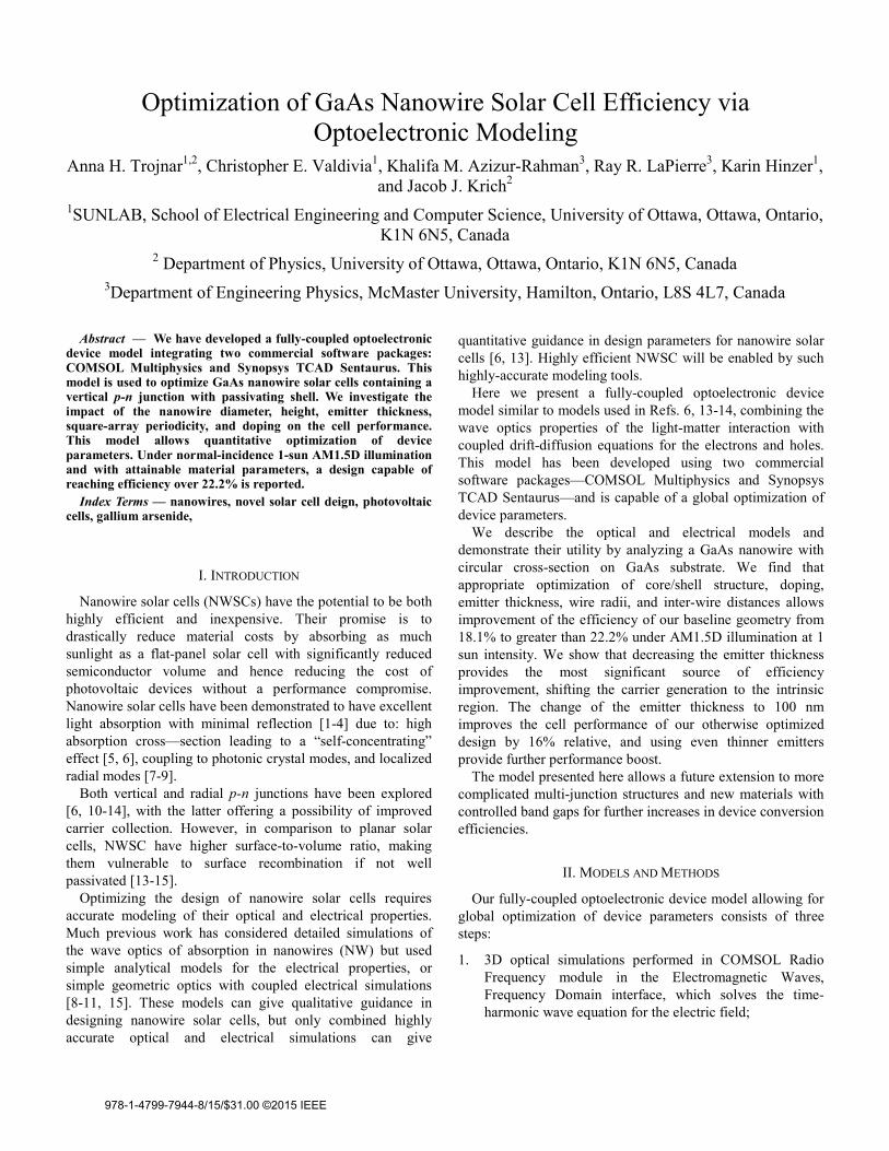
Fig. 2. NWSC efficiency as a function of NW array pitch for d/a ratio of 0.5 (solid line), 0.6 (dotted line) and 0.4 (dashed line) with three different surface recombination velocities S: 0 cm/s (blue), 1·10
3 cm/s (red), and 3·10
5 cm/s (grey). Curves with S=3·10
5 cm/s
are plotted on the secondary y-axis.
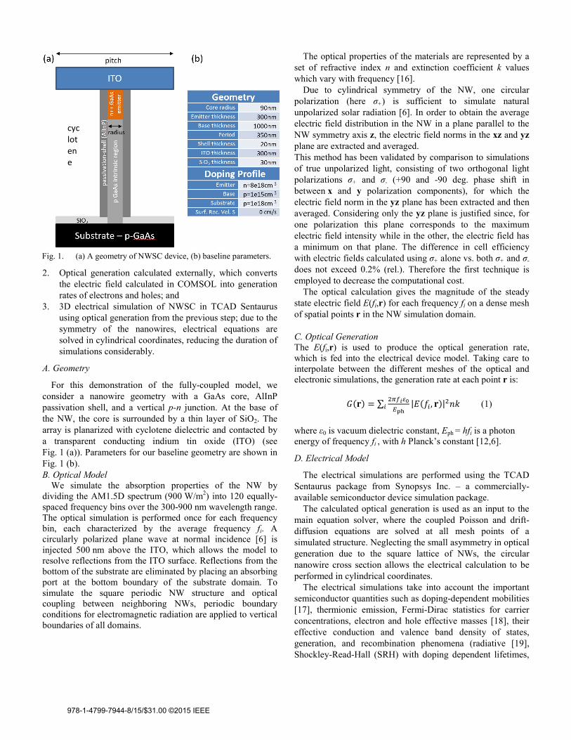
Fig. 3. Maximum achievable photo-generated Jph for three NW diameter/pitch ratios as a function of NW array pitch. Jph is independent of surface recombination velocity.
and Auger [18]). The model also includes doping dependent bandgap narrowing [20] for GaAs and a surface recombination on the GaAs/AlInP shell interface.
SRH lifetimes are calculated using the Scharfetter relation:
�������,�, � ,�! � �"�# $ �%&' ( �%)*
1 $ ,��,� $ � ,��-./
01 ,
with maximum lifetimes for carriers set to be τmax,e=1·10-6 s, and τmax,h=2·10-8 s, and minimum τmin,e=τmin,h=0 s. These parameters, γ=1, together with Nref,e=1016 cm-3 and Nref,h=2·1018 cm-3 result in SRH lifetimes for electron (hole) of ~10 (20) ns in the emitter, 500 (20) ns in the intrinsic region, and 2 (1) ns in the substrate.
Surface recombination is defined as:
234-/,*.5678 � �9 ( �),.//�
�� $ �:�;�
$ �9 $ 9:�;*
,
where
�: � �),.// exp ,�5-&��? 0 ; 9 � 9),.// exp ,(�5-&�
�? 0, with �),.//� � ��9� being an intrinsic carrier concentration, where n0 (p0) are the electron (hole) equilibrium concentrations. �5-&� is the trap energy measured from the intrinsic energy. We choose Etrap=0. The recombination velocities in general depend on the concentration of interface states at the interface, however we choose to set a single surface recombination velocity sp=sn=S for convenience.
Note that we use doping dependent bandgap (Eg) narrowing in the electrical simulations, but not in the optical ones. The effective shrinkage of Eg occurs due to existence of band tails within Eg, and hence result in the lowered open circuit voltage Voc of the solar cell. At the same time, carriers excited to these localized states do not contribute towards the electrical
current, hence there is no need to consider below-bandgap absorption. We believe this pessimistic combination of assumptions best reflects the real device properties.
III. RESULTS
We report on the influence of the surface recombination on the optimal NW geometry exploring different NW array pitch and NW diameters. We find optimal NW doping, and explore different depths of emitter-intrinsic region interface. We find that the performance of a new design, optimized using our coupled model, even in the presence of realistic surface recombination, exceeds the performance of the baseline model geometry (Fig. 1 (b)), optimized using previous uncoupled modeling [12, 15]. We show that decreasing the emitter thickness is the most significant source of improvement in the optimizations, shifting the carrier generation to the intrinsic region. Using optimized cell design with emitter thickness of 100 nm [6] with realistic, well passivated surface (S = 1·103 cm/s) gives 22.2% efficiency, hence the change of only the emitter thickness improves the cell performance of our otherwise optimized design by 16% relative.
The baseline NWSC defined in Fig. 1 has an efficiency of 18.1% in the absence of any GaAs/AlInP surface recombination. Optimization of the doping of nanowires with this geometry led to a nanowire solar cell with 19.4% efficiency—1.3% (abs.) higher efficiency than the baseline. The optimized doping included: decreased doping of the emitter to n=1·1018 cm-3, increased base doping to p=1·1016 cm-3 and increased substrate doping to p=5·1018 cm-3. This change increases carrier lifetime in the emitter, while maintaining strong drift current in the intrinsic region. This is of particular importance since carriers are predominantly generated in or near the emitter.
Without surface passivation, surface recombination velocities near S=3·105 cm/s have been found previously [6].
978-1-4799-7944-8/15/$31.00 ©2015 IEEE
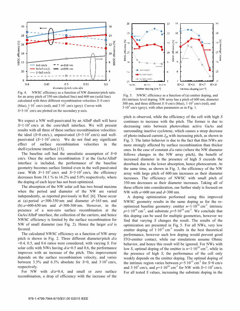
Fig. 4. NWSC efficiency as a function of NW diameter/pitch ratio for an array pitch of 350 nm (dashed line) and 600 nm (solid line) calculated with three different recombination velocities S: 0 cm/s (blue), 1·10
3 cm/s (red), and 3·10
5 cm/s (grey). Curves with
S=3·105 cm/s are plotted on the secondary y-axis.
Fig. 5. NWSC efficiency as a function of (a) emitter doping, and (b) intrinsic level doping. NW array has a pitch of 600 nm, diameter 300 nm, and three different S: 0 cm/s (blue), 1·103 cm/s (red), and 3·105 cm/s (grey), with other parameters as in Fig. 1.
We expect a NW well-passivated by an AlInP shell will have S=1·103 cm/s at the core/shell interface. We will present results with all three of these surface recombination velocities: the ideal (S=0 cm/s.), unpassivated (S=3·105 cm/s) and well-passivated (S=1·103 cm/s). We do not find any significant effect of surface recombination velocities in the shell/cyclotene interface [13].
The baseline cell had the unrealistic assumption of S=0 cm/s. Once the surface recombination S at the GaAs/AlInP interface is included, the performance of the baseline geometry becomes surface limited even in the well-passivated case. With S=1·103 cm/s and S=3·105 cm/s, the efficiency decreases from 18.1 % to 16.2% and 5.0% respectively, where the doping of each layer has not been optimized.
The absorption of the NW solar cell has two broad maxima when the period and diameter of the NW are varied independently, as reported previously in Ref. [6]. These occur at (a) period a=300-350 nm and diameter d=165 nm, and (b) a=600-650 nm and d=300-360 nm. However, in the presence of a non-zero surface recombination at the GaAs/AlInP interface, the collection of the carriers, and hence NWSC efficiency is limited by the surface recombination for NW of small diameter (see Fig. 2). Hence the larger a/d is favored.
The calculated NWSC efficiency as a function of NW array pitch is shown in Fig. 2. Three different diameter/pitch d/a =0.4, 0.5, and 0.6 ratios were considered, with varying S. For solar cells with NWs having d/a=0.5 and 0.6, the performance improves with an increase of the pitch. This improvement depends on the surface recombination velocity, and varies between 3.3% and 6.3% absolute for S=0, and 3·105 cm/s, respectively.
For NW with d/a=0.4, and small or zero surface recombination, a drop of efficiency with the increase of the
pitch is observed, while the efficiency of the cell with high S continues to increase with the pitch. The former is due to decreasing ratio between photovoltaic active GaAs and surrounding inactive cyclotene, which causes a steep decrease of photo-induced current Jph with increasing pitch, as shown in Fig. 3. The latter behavior is due to the fact that thin NWs are more strongly affected by surface recombination than thicker ones. In the case of constant d/a ratio (where the NW diameter follows changes in the NW array pitch), the benefit of increased diameter in the presence of high S exceeds the drawback due to the lower absorption, hence photocurrent. At the same time, as shown in Fig. 3, the efficiency of the NW array with large pitch of 600 nm increases as their diameter increases. The efficiency of NWSC with small pitch of 350 nm decreases as their diameter increases. Taking all of these effects into consideration, our further study is focused on NW with a=600 nm and d=300 nm.
A doping optimization performed using this improved NWSC geometry results in the same doping as for the re-optimized baseline geometry: emitter n=1·1018 cm-3
, intrinsic p=1·1016 cm-3, and substrate p=5·1018 cm-3. We conclude that this doping can be used for multiple geometries, however we find that varying S changes the result. The results of the optimization are presented in Fig. 5. For all NWs, very low emitter doping of 1·1015 cm-3 results in the best theoretical performance, however such low doping would prevent good ITO-emitter contact, while our simulations assume Ohmic behavior, and hence this result will be ignored. For NWs with low S, optimal doping of the emitter is n=1·1018 cm-3, while in the presence of high S, the performance of the cell only weakly depends on the emitter doping. The optimal doping of the intrinsic region varies between p=5·1015 cm-3 for S=0 cm/s and 3·105 cm/s, and p=1·1016 cm-3 for NW with S=1·103 cm/s. For all tested S values, increasing the substrate doping in the
978-1-4799-7944-8/15/$31.00 ©2015 IEEE
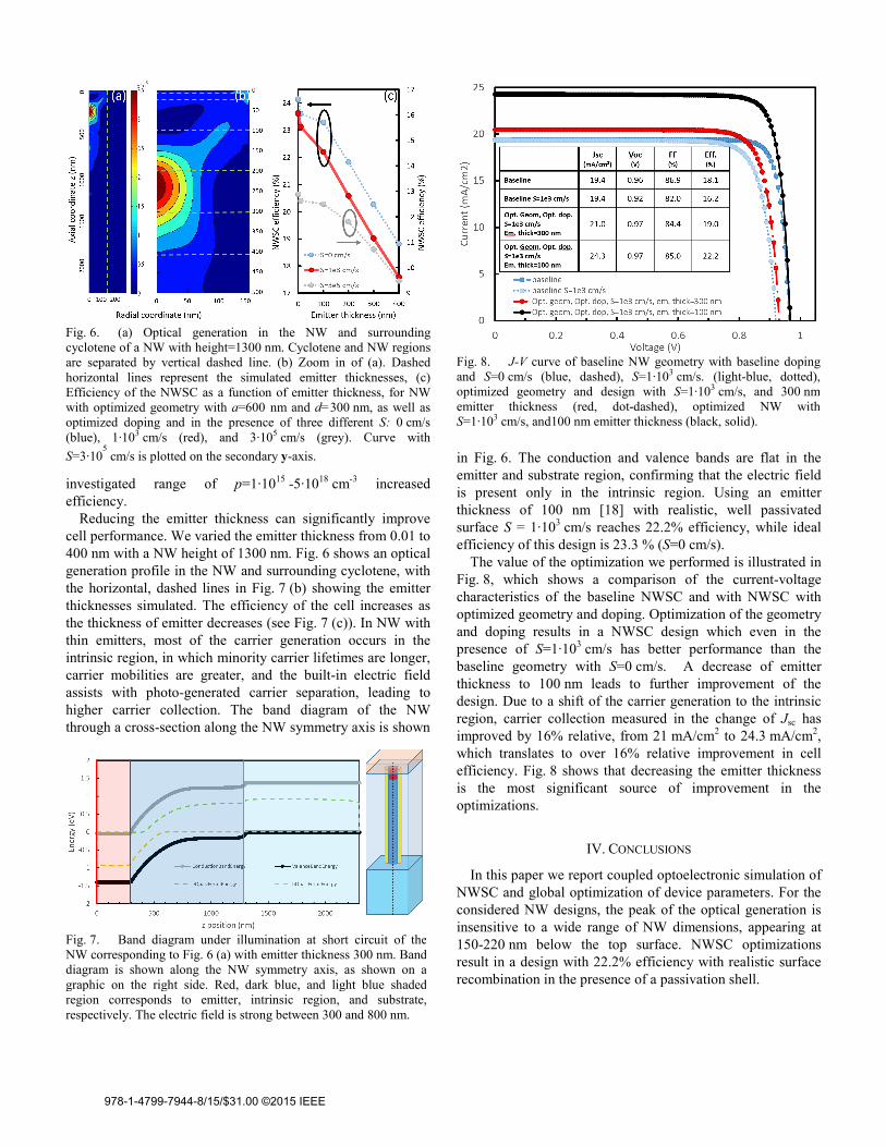
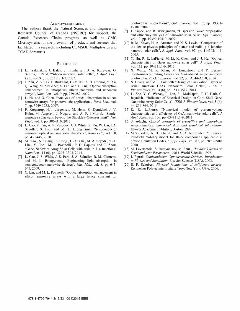
Fig. 7. Band diagram under illumination at short circuit of the NW corresponding to Fig. 6 (a) with emitter thickness 300 nm. Band diagram is shown along the NW symmetry axis, as shown on a graphic on the right side. Red, dark blue, and light blue shaded region corresponds to emitter, intrinsic region, and substrate, respectively. The electric field is strong between 300 and 800 nm.
Fig. 6. (a) Optical generation in the NW and surrounding cyclotene of a NW with height=1300 nm. Cyclotene and NW regions are separated by vertical dashed line. (b) Zoom in of (a). Dashed horizontal lines represent the simulated emitter thicknesses, (c) Efficiency of the NWSC as a function of emitter thickness, for NW with optimized geometry with a=600 nm and d=300 nm, as well as optimized doping and in the presence of three different S: 0 cm/s (blue), 1·103 cm/s (red), and 3·105 cm/s (grey). Curve withS=3·10
5 cm/s is plotted on the secondary y-axis.
investigated range of p=1·1015 -5·1018 cm-3 increased efficiency.
Reducing the emitter thickness can significantly improve cell performance. We varied the emitter thickness from 0.01 to 400 nm with a NW height of 1300 nm. Fig. 6 shows an optical generation profile in the NW and surrounding cyclotene, with the horizontal, dashed lines in Fig. 7 (b) showing the emitter thicknesses simulated. The efficiency of the cell increases as the thickness of emitter decreases (see Fig. 7 (c)). In NW with thin emitters, most of the carrier generation occurs in the intrinsic region, in which minority carrier lifetimes are longer, carrier mobilities are greater, and the built-in electric field assists with photo-generated carrier separation, leading to higher carrier collection. The band diagram of the NW through a cross-section along the NW symmetry axis is shown
in Fig. 6. The conduction and valence bands are flat in the emitter and substrate region, confirming that the electric field is present only in the intrinsic region. Using an emitter thickness of 100 nm [18] with realistic, well passivated surface S = 1·103 cm/s reaches 22.2% efficiency, while ideal efficiency of this design is 23.3 % (S=0 cm/s).
The value of the optimization we performed is illustrated in Fig. 8, which shows a comparison of the current-voltage characteristics of the baseline NWSC and with NWSC with optimized geometry and doping. Optimization of the geometry and doping results in a NWSC design which even in the presence of S=1·103 cm/s has better performance than the baseline geometry with S=0 cm/s. A decrease of emitter thickness to 100 nm leads to further improvement of the design. Due to a shift of the carrier generation to the intrinsic region, carrier collection measured in the change of Jsc has improved by 16% relative, from 21 mA/cm2 to 24.3 mA/cm2, which translates to over 16% relative improvement in cell efficiency. Fig. 8 shows that decreasing the emitter thickness is the most significant source of improvement in the optimizations.
IV. CONCLUSIONS
In this paper we report coupled optoelectronic simulation of NWSC and global optimization of device parameters. For the considered NW designs, the peak of the optical generation is insensitive to a wide range of NW dimensions, appearing at 150-220 nm below the top surface. NWSC optimizations result in a design with 22.2% efficiency with realistic surface recombination in the presence of a passivation shell.
Fig. 8. J-V curve of baseline NW geometry with baseline dopingand S=0 cm/s (blue, dashed), S=1·103 cm/s. (light-blue, dotted), optimized geometry and design with S=1·103 cm/s, and 300 nm emitter thickness (red, dot-dashed), optimized NW with S=1·103 cm/s, and100 nm emitter thickness (black, solid).
978-1-4799-7944-8/15/$31.00 ©2015 IEEE
ACKNOWLEDGEMENT The authors thank the Natural Sciences and Engineering
Research Council of Canada (NSERC) for support, the Canada Research Chairs program, as well as CMC Microsystems for the provision of products and services that facilitated this research, including COMSOL Multiphysics and TCAD Sentaurus.
REFERENCES
[1] L. Tsakalakos, J. Balch, J. Fronheiser, B. A. Korevaar, O. Sulima, J. Rand, “Silicon nanowire solar cells”, J. Appl. Phys. Lett., vol. 91, pp. 233117:1-3, 2007.
[2] J. Zhu, Z. Yu, G. F. Burkhard, C.-M Hsu, S. T. Connor, Y. Xu, Q. Wang, M. McGehee, S. Fan, and Y. Cui, “Optical absorption enhancement in amorphous silicon nanowire and nanocone arrays”, Nano Lett., vol. 9, pp. 279-282, 2009.
[3] L. Hu and G. Chen, “Analysis of optical absorption in silicon nanowire arrays for photovoltaic application”, Nano Lett., vol. 7, pp. 3249-3252, 2007.
[4] P. Krogstrup, H. I. Jørgensen, M. Heiss, O. Demichel, J. V. Holm, M. Aagesen, J. Nygard, and A. F. i Morral, “Single-nanowire solar cells beyond the Shockley–Queisser limit”, Nat. Phot., vol. 7, pp. 306–310, 2013.
[5] L. Cao, P. Fan, A. P. Vasudev, J. S. White, Z. Yu, W. Cai, J.A. Schuller, S. Fan, and M. L. Brongersma, “Semiconductor nanowire optical antenna solar absorbers”, Nano Lett., vol. 10, pp. 439-445, 2010.
[6] M. Yao , N. Huang , S. Cong , C.-Y. Chi , M. A. Seyedi , Y.-T. Lin , Y. Cao , M. L. Povinelli , P. D. Dapkus, and C. Zhou, “GaAs Nanowire Array Solar Cells with Axial p–i–n Junctions” Nano Lett., 14 (6), pp. 3293–3303, 2014.
[7] L. Cao, J. S. White, J. S. Park, J. A. Schuller, B. M. Clemens, and M. L. Brongersma, “Engineering light absorption in semiconductor nanowire devices”, Nat. Mat., vol. 8, pp. 643-647, 2009.
[8] C. Lin, and M. L. Povinelli, “Optical absorption enhancement in silicon nanowire arrays with a large lattice constant for
photovoltaic applications”, Opt. Express, vol. 17, pp. 19371-19381, 2009.
[9] J. Kupec, and B. Witzigmann, “Dispersion, wave propagation and efficiency analysis of nanowire solar cells”, Opt. Express, vol. 17, pp. 10399-10410 ,2009.
[10] B. M. Kayes, H. A. Atwater, and N. S. Lewis, “Comparison of the device physics principles of planar and radial p-n junction nanorod solar cells”, J. Appl. Phys., vol. 97, pp. 114302:1-11, 2005.
[11] Y. Hu, R. R. LaPierre, M. Li, K. Chen, and J.-J. He, “Optical characteristics of GaAs nanowire solar cell”, J. Appl. Phys., vol. 112, pp. 104311:1-6, 2012.
[12] X. Wang, M. R. Khan, M. Lundstrom, and P. Bermel, “Performance-limiting factors for GaAs-based single nanowire photovoltaics”, Opt. Express, vol. 22, pp. A344-A358, 2014.
[13] N. Huang, and M. L. Povinelli “Design of Passivation Layers on Axial Junction GaAs Nanowire Solar Cells”, IEEE J. Photovoltaics, vol. 4 (6), pp. 1511-1517, 2014.
[14] L. Zhe, Y. C. Wenas,, F. Lan, S. Mokkapati, T. H. Hark, C. Jagadish, “Influence of Electrical Design on Core–Shell GaAs Nanowire Array Solar Cells”, IEEE J. Photovoltaics, vol. 5 (6), pp. 854-864, 2015.
[15] R. R. LaPierre, “Numerical model of current-voltage characteristics and efficiency of GaAs nanowire solar cells”, J. Appl. Phys., vol. 109, pp. 034311:1-9, 2011.
[16] S. Adachi, Optical constants of crystalline and amorphous semiconductors: numerical data and graphical information, Kluwer Academic Publisher, Boston, 1999.
[17] M.Sotoodeh, A. H. Khalid, and A. A. Rezazadeh, “Empirical low-field mobility model for III–V compounds applicable in device simulation Codes J. Appl. Phys., vol. 87, pp. 2890-2900, 2000.
[18] M. Levinshtein, S. Rumyantsev, M. Shur , Handbook Series on Semiconductor Parameters, Vol I, World Scietific, 1996.
[19] J. Piprek, Semiconductor Optoelectronic Devices: Introduction to Physics and Simulation, Elsevier Science (USA), 2003.
[20] E. F. Schubert, Physical foundations of solid-state devices, Rensselaer Polytechnic Institute Troy, New York, USA, 2006.
978-1-4799-7944-8/15/$31.00 ©2015 IEEE


![GaAs and InGaAs Single Electron Hexagonal Nanowire ...€¦ · Q-LSIs based on the binary-decision-diagram (BDD) logic architecture[3], using arrays of GaAs and InGaAs SE BDD node](https://img.pdfslide.net/doc/110x75/5f8f1c35fcaa4a5a3265bd37/gaas-and-ingaas-single-electron-hexagonal-nanowire-q-lsis-based-on-the-binary-decision-diagram.jpg)
![Emergence of localized states in narrow GaAs/AlGaAs nanowire quantum well tubes · 2020-02-24 · grown wires[12,13,14]. In addition, 0D quantum dots formed by Stranski-Krastinow-like](https://img.pdfslide.net/doc/110x75/5f0e3fc37e708231d43e53ef/emergence-of-localized-states-in-narrow-gaasalgaas-nanowire-quantum-well-tubes.jpg)