Embed Size (px)
Citation preview
PRZEGLĄD ELEKTROTECHNICZNY (Electrical Review), ISSN 0033-2097, R. 87 NR 4/2011 279
Saud NAQVI1, Rameez NAQVI2, Raja Ali RIAZ1,3, Faisal SIDDIQUI1
COMSATS Pakistan (1), TU Wein University of Vienna (2), University of Southampton (3)
Optimized RTL design and implementation of LZW algorithm for high bandwidth applications
Abstract. This paper presents a high-speed low-complexity Register Transfer Logic (RTL) design and implementation of the lossless Lempel-Ziv-Welch (LZW) algorithm on Xilinx Virtex II device family for High Bandwidth Applications. Comparative analysis of the proposed design with the established commercial data compression and decompression accelerators show that the proposed design offers comparatively high throughput 1.42 Gbits/s, elevated throughput/slice value 151.8 Kbytes/s/slice and lower operational power requirements 333 mW. Streszczenie. W artykule zaprezentowano nieskomplikowany, wysokiej częstotliwości projekt obwodu RTL oraz bezstratny algorytm LZW z układem Xilinx Virtex II. Porównano zaproponowany układ z komercyjnymi układami kompresji i stwierdzono, że umożliwia on przepustowość 1.42 Gbit/s przy poborze mocy 333 mW. (Optymalizowany układ RTL i algorytm LZW w zastosowaniach szerokopasmowych). Keywords: Lossless Compression, Lempel-Ziv-Welch, LUTs and Throughput/Slice. Słowa kluczowe: in the case of foreign Authors in this line the Editor inserts Polish translation of keywords.
Introduction
Data compression is a defined method or encoding technique which substantially reduces data size according to some existing rules [1, 2]. According to application area, two different classes of compression are used namely; lossy data compression and lossless data compression. Lossy data compression is generally used for applications like image and audio file types, where loss of information is less important [2]. Conversely, lossless data compression is most adaptable to applications like data transmission and storage, where it is important to keep all the information intact [2]. A wide variety of lossless compression algorithms have been proposed in the past which include Limpel and Ziv (L Z) codes [3], Huffman codes [4], Adaptive Huffman [5], Run-length encoding [6], Arithmetic coding [7], Multigroup compression method [8, 9], Shannon-Fano code [10], and dictionary-based methods [11-14]. Some important applications include storage systems (hard disks, tapes and file servers) and communication networks (LAN, WAN, wireless) [15]. LZW algorithm [16], one of the variations of the LZ algorithm is the most famous because of its simplicity and efficient compression ratios [2].
The major issues in harnessing the performance of compression in high bandwidth data communication network applications running over 1 Gbits/s require optimized data compression hardware [15]. Various accelerators have been proposed by different manufacturers in the past. Some famous devices are Improved LZW VLSI Processor [17] which implements the New LZW algorithm and presents a throughput of 198.4 Mbytes/s at 124 MHz clock using 90-nm CMOS process technology, LZWR3 Core by Helion [18] provides a combined throughput of 84.75 Mbytes/s clocked at 103 MHz and implemented in 90-nm CMOS technology, the ELDC-3 core [19] has a throughput of 50-66 Mbytes/s implemented in a 90-nm CMOS technology and clocked at 75 MHz, X-MatcPROv4 [15] from Loughborough University presents an attractive throughput of 200 Mbytes/s working at a clock rate of 50 MHz and implemented in 0.18 micron SRAM-CMOS technology, PDLZW−AHDB[1] gives a comparative throughput of 16.7−125 Mbytes/s for compression and 25−83 Mbytes/s for decompression clocked at 100 MHz and implemented in 0.35 micron technology.
This paper presents an optimized implementation of the LZW algorithm and reports the significant features of the design; that make it outperform the previous designs in terms of various implementation parameters. The proposed design presents an efficient implementation of the primitive
LZW algorithm, tailor made for high bandwidth applications. The architectural details presented in the next sections highlight that, how the design optimizations in terms of area and speed take full advantage of the simplicity and high compression efficiencies of the LZW algorithm. The proposed design takes full advantage of the inherent synchronization between the two processes and presents an efficient dictionary based implementation making the design possible to achieve high throughputs over 1 Gbits/s with great efficiency.
The rest of the paper is organized as follows. System Design section, presents the overall system model and individually discusses the detailed architectural aspects and RTL level designs of the compression and decompression modules. The flow of the algorithms and photograph codes represent the stepwise execution of events for both designs respectively. Results and Discussion section, highlights the implementation details of individual and overall designs with respect to the target device. It also provides a detailed comparison of the proposed design with previous implementations showing how the current design outperforms the rest. Finally, some conclusions are made in the final section.
System Design This section presents the architectural details of the proposed accelerator design, responsible for achieving high throughputs at the cost of considerably low system complexity. The proposed design is targeted to sustain remarkably high throughputs having the emphasis of realizing it with the minimum possible logic, hence limiting the complexity of the design. Proposed accelerator architecture is able to operate in three independent modes, namely Compression-only mode, Decompression-only mode and Full-duplex mode. The detailed operation and performance parameters related to the proposed architecture are discussed in subsequent sections. Compression architecture This section presents the detailed RTL level architecture of the proposed compression design. The compression architecture efficiently models the standard lossless LZW compression by Terry A. Welch [16] with major optimizations. As the number of entries in the dictionary, robustly affects the resulting compression ratio [15] therefore the effective dictionary size is optimally selected to suite versatile applications [16]. The dictionary locations are coded in such a resourceful manner that minimal bits are required to code a particular location thus achieving higher compression ratios.
280 PRZEGLĄD ELEKTROTECHNICZNY (Electrical Review), ISSN 0033-2097, R. 87 NR 4/2011
Fig.1. The Compression Architecture
Figure 1 shows the detailed schematic of the compression architecture. The compression architecture encompasses four major blocks: the Node formation logic, Data Dictionary, Comparison logic and Code generation logic.
Node formation logic The node formation logic is responsible for generating
larger nodes (dictionary entries) by using combination of current and previous input. It comprises of three 8 bit registers and selection dependent concatenation logic. The maximum size of the node is limited by the width of the Data Dictionary. A New Node can be formed in a number of possible ways, depending upon the selection input coming from the controller. Lower 32 bits are reserved for the created Node; bits 32 and 33 are reserved for encoding the length of each node thus specifying the valuable information within a node required at decompression side.
Data dictionary The data dictionary’s capacity c is optimally selected to be 4096x35 implemented with four dual port block rams. Each dictionary entry is 35 bits wide limiting the maximum size of a node. Additional to storing data information; each dictionary entry stores two extra bits representing the length of the stored node and a valid bit which specifies the validity of information stored at that particular entry. The valid bit accelerates the search process by limiting the number of entries to be searched each time. Therefore the dictionary search time t_D is reduced from t_s to t_ve. Where t_s is the time to search the whole dictionary and t_ve represents the time to search the valid entries only. Dictionary search process is further optimized by implementing the 4K dictionary with four dual port ram modules. All rams are searched in parallel using the same address generation logic. Each ram module outputs two consecutive dictionary words at a time which are sent to comparison logic for a match. At a time 8 words are searched in parallel. Therefore the whole dictionary can be searched in 1024 comparisons. The dictionary is maintained in sequential order and the rams are updated in sequence. Dictionary search process is further optimized by efficient design of the comparator logic presented in the next subsection. Figure 1 shows the implementation of block ram based implementation of
dictionary. Each dual port block ram can be addressed in read mode by placing Read_Addr and Read_Addr1 at the rams address inputs. When writing to the ram, a multiplexer at the Ram_Addr2 input selects between Read_Addr1 and Write_Addr depending upon the selection input from the decoder logic. A 2 − 4 decoder and a small logic selects the ram to be written depending upon the Dec_in input and the Dic_we control signals from the controller. When an output code is formed, only 10 bits are used to encode a dictionaries location which can be easily decoded at the decompression end by effective synchronization process between the two dictionaries.
Comparison logic The comparison logic is optimized for high-speed dictionary searching by decomposing the searching process into hierarchal steps. In order to minimize the search complexity O(log 2(dictionarylength/4)) and search time t_D the comparison logic first compares the valid bit portion of each dictionary entry to confirm the validity of a node. If a valid bit for an entry is zero then no further comparison is done, limiting the propagation delay for one entry to a single XNOR gate. Otherwise, the node length NL for each dictionary entry is compared. If comparison is true only then the corresponding data portion is compared to the input reducing the propagation delay to two XNOR gates for each dictionary entry in case of a mismatch. Figure 1 shows the single entry comparison process for the single bit output Comp_out0. Eight entries are compared with the input at a time and the corresponding comparison outputs (Comp out0. . .Comp out7) are fed to encoder logic, which encodes the particular block ram that gave the correct match depending on the comparator logic output. The latter information is used by the code generation logic and lately at decompression end. Code generation logic Code generation logic is responsible for assembling the compressed output code Comp_o/p_code. Read_Addr, NLC_out[7 : 0] and Enc_op are inputs to the code gene-ration logic. A comparator logic decides the formation of the Comp_o/p_code depending upon Read_Addr. If Read_Addr from Dic_Read_Address Logic is smaller than 256 (which mean a single byte is matched) then Comp_o/p_code is

PRZEGLĄD ELEKTROTECHNICZNY (Electrical Review), ISSN 0033-2097, R. 87 NR 4/2011 281
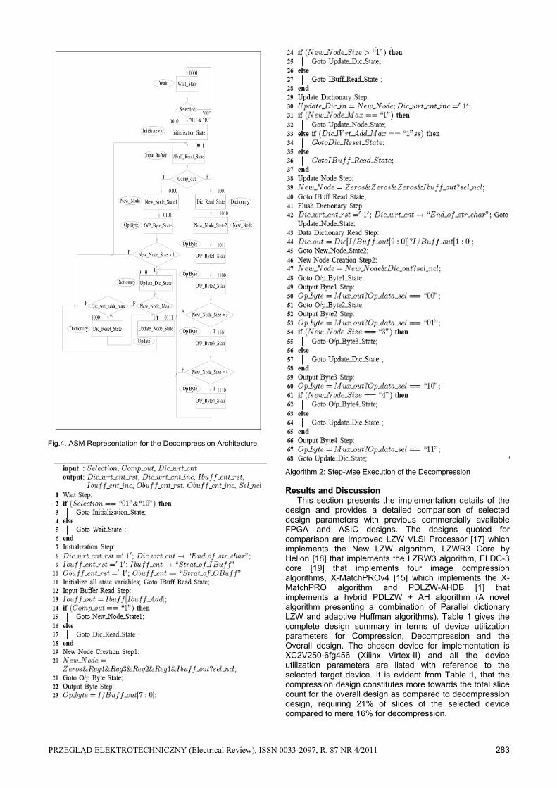
formed by concatenating the data byte from NLC with four zeros and a bit indicating a single byte. Otherwise, 10−bit Read_Addr, Enc_op and a bit indicating dictionary address are concatenated and mapped to the Comp_o/p_code. Figure 2 gives the ASM translation of the compression algorithm. The photograph code of Algorithm 1. describes the realization of the step-wise working of compression algorithm in a defined sequence or states. The compression process activates on receiving an external selection input.
Fig.2. ASM Representation for the Compression Architecture
After initialization Step-wise Execution of the all state variables the Input Step-wise Execution of the Compression Algorithm buffer is read for node creation process. A new node is formed by the node creation logic depending upon the control input from the controller module. Newly formed node is to dictionary state after reading the dictionaries current entry. Result of the comparison decides whether the node is already present in the dictionary or needs to be created. If a match is found, respective compression code is sent to the output; otherwise the dictionary is searched again until a match is found. In case of no match after a complete dictionary search, the dictionary is updated with the respective node. The dictionary is reset every time it gets completely filled and the refilling process starts with the new (current) data window. The detailed hierarchal execution of events is listed in the photograph code. Decompression Architecture Decoding Logic This section presents the detailed RTL level architecture of the proposed decompression design. The decompression architecture operates in perfect synchronism with the compression architecture. The dictionaries at both ends are ensured to be effectively synchronized [16]. As a result of symmetric synchronism, the decompression design is relatively simpler and similar with potentially complex control. The major design requirement at the
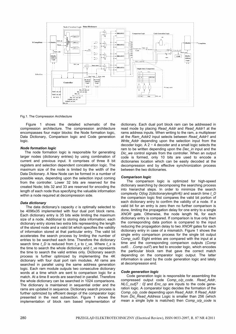
decompression end is to effectively decode the incoming Compressed_ data and send it to the output maintaining the Data Dictionary in a similar fashion. Figure 3 shows the detailed architecture of the decompression design. The decompression architecture consists of four major blocks: the Node Formation Logic, Data Dictionary, Decoding Logic and Output Data Logic.
Algorithm 1 Step-wise Execution of the Compression Algorithm
282 PRZEGLĄD ELEKTROTECHNICZNY (Electrical Review), ISSN 0033-2097, R. 87 NR 4/2011
Fig.3. The Decompression Architecture Node formation logic Exactly similar dictionary entries are to be created at decompression end in order to make the dictionaries exactly synchronous at both ends. Therefore the node formation process is almost similar. There are two major variations from the compression design. 1) An extra 8−bit register is included in the node formation logic which is used to store the most significant byte of a node, so that all the separate bytes constituting a node can be sent at the output one at a time. 2) A node read from the dictionary is also added as an input (Dic_out) to the node creation logic so that it can be sent at the output and used for creating bigger nodes. The rest of the process is exactly coupled with the compression design so that exactly similar nodes are created.
Data dictionary The data dictionary is maintained in a similar fashion and the logic required to update the dictionary is almost similar. The reading process is quite different as an entry needs not to be searched but read at the exact address supplied by the output of the compression design. As the dictionary can be directly read by decoding the input (Compressed_data) there is no requirement of extra reading logic. A 4K Data Dictionary is implemented using four single port block RAMS. Figure 3 shows the block ram based implementation of dictionary. Each single port block ram can be addressed in read mode by placing Read_Addr at the ram’s single address input. A 2-1 multiplexer at the rams address input decides whether Read_Addr or Write_Addr is to be placed depending upon the comparator output from decoding logic. A 2−4 decoder and a small logic select the ram to be written depending upon the Dec_in input and the Dic_we control signals from the controller. When reading a node, the exact 10−bit Read_Addr from the decoding logic is placed at all the rams address input and a single location is selected from four ram outputs at Dic_out providing the node to be sent to the output.
Decoding Logic The small decoding logic decides whether the incoming
data is a byte to be sent to the output directly; or a
dictionaries address containing the encoded address of a node. It does so by checking the most significant bit of the input I/Buff_out. If it is a ”1”, the incorporated uncompressed byte is extracted and sent to the output data logic. Otherwise, the 10 – bit dictionaries address is decoded and sent to the data dictionary for the node to be read. In this way, the decoding logic instructs the output data logic to output the required byte sequence.
Output data logic The output data logic is responsible for sending the uncompressed data in correct byte-order at the output. It is operated in two modes depending upon the input Comp_out from decoding logic. If it is ”0”, one of the bytes from node creation logic is sent to the output depending upon the Op_data_sel input from the controller. Otherwise, uncompressed byte coming from the decoding logic is sent to Op_byte. Figure 4 gives the ASM translation of the decompression algorithm. The photograph code for Algorithm 2. describes the realization of the step-wise working of decompression algorithm in a defined sequence. The decompression process is also triggered by the same external selection input. After Initialization of all state variables, the Input buffer is read and the input data is decoded to decide whether it is a single byte or address of a node. If input is a single byte it is sent to the output after formation of new node. Afterwards, it is further checked that whether the newly formed node’s size is greater than ”1” or not. In case of a positive result the dictionary is updated and either the node is updated or dictionary is flushed afterwards, depending upon specific state conditions. In case the decoded input turns out to be a valid dictionary address, the dictionary is read using the particular address and subsequent bytes are sent to the output; one by one preceded by a unique node formation process defined in the photograph code. After sending correct pattern of bytes to the output, the dictionary is updated. The detailed hierarchal execution of events is listed in the photograph code.
PRZEGLĄD ELEKTROTECHNICZNY (Electrical Review), ISSN 0033-2097, R. 87 NR 4/2011 283
Fig.4. ASM Representation for the Decompression Architecture
Algorithm 2: Step-wise Execution of the Decompression Results and Discussion
This section presents the implementation details of the design and provides a detailed comparison of selected design parameters with previous commercially available FPGA and ASIC designs. The designs quoted for comparison are Improved LZW VLSI Processor [17] which implements the New LZW algorithm, LZWR3 Core by Helion [18] that implements the LZRW3 algorithm, ELDC-3 core [19] that implements four image compression algorithms, X-MatchPROv4 [15] which implements the X-MatchPRO algorithm and PDLZW-AHDB [1] that implements a hybrid PDLZW + AH algorithm (A novel algorithm presenting a combination of Parallel dictionary LZW and adaptive Huffman algorithms). Table 1 gives the complete design summary in terms of device utilization parameters for Compression, Decompression and the Overall design. The chosen device for implementation is XC2V250-6fg456 (Xilinx Virtex-II) and all the device utilization parameters are listed with reference to the selected target device. It is evident from Table 1, that the compression design constitutes more towards the total slice count for the overall design as compared to decompression design, requiring 21% of slices of the selected device compared to mere 16% for decompression.
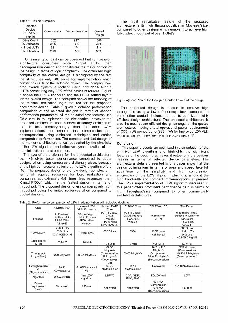
284 PRZEGLĄD ELEKTROTECHNICZNY (Electrical Review), ISSN 0033-2097, R. 87 NR 4/2011
Table 1. Design Summary
On similar grounds it can be observed that compression
architecture consumes more 4-input LUT’s than decompression design and constitutes the major portion of the design in terms of logic complexity. The optimized logic complexity of the overall design is highlighted by the fact that it requires only 586 slices for implementation which constitutes 38% of the selected device. The compact low-area overall system is realized using only 1114 4-input LUT’s constituting only 36% of the device resources. Figure 5 shows the FPGA floor-plan and the FPGA routed layout for the overall design. The floor-plan shows the mapping of the minimal realization logic required for the proposed accelerator design. Table 2 gives a detailed performance comparison of the selected designs in terms of chosen performance parameters. All the selected architectures use CAM circuits to implement the dictionaries, however the proposed architecture uses a novel dictionary architecture that is less memory-hungry than the other CAM implementations but enables fast compression and decompression using optimized techniques and exhibit comparable performances. The compact and fast design of the memory architecture is well supported by the simplicity of the LZW algorithm and effective synchronization of the parallel dictionaries at both ends.
The size of the dictionary for the presented architecture i.e. 4kB gives better performance compared to quote designs when using comparable dictionary sizes, because of the high compression ratios that the LZW algorithm offers [16]. The proposed design offers low design complexity in terms of required resources for logic realization and consumes approximately 4.8 times less resources than XmatchPROv4 which is the fastest design in terms of throughput. The proposed design offers comparatively high throughput using the limited resources when compared to quoted designs.
The most remarkable feature of the proposed architecture is its high throughput/slice in Mbytes/s/slice, compared to other designs which enable it to achieve high full-duplex throughput of over 1 Gbit/s. Fig. 5. a)Floor Plan of the Design b)Routed Layout of the design
The presented design is tailored to achieve high throughputs using a lower frequency clock compared to some other quoted designs; due to its optimized highly efficient design architecture. The proposed architecture is also the most power efficient design amongst all the quoted architectures, having a total operational power requirements of (333 mW) compared to (865 mW) for Improved LZW VLSI Processor and (671 mW, 694 mW) for PDLZW-AHDB [1]. Conclusion This paper presents an optimized implementation of the primitive LZW algorithm and highlights the significant features of the design that makes it outperform the pevious designs in terms of selected device parameters. The architectural details presented in this paper show that the design optimizations in terms of area and speed take full advantage of the simplicity and high compression efficiencies of the LZW algorithm placing it amongst the high bandwidth and compact implementations at present. The FPGA implementation of LZW algorithm discussed in this paper offers prominent performance gain in terms of high throughput/slice compared to other commercially available architectures.
Table 2. Performance comparison of LZW implementation with selected designs
Chip X-MatchProv4 Improved LZW VLSI Processor
Helion LZWR3 Core
ELDC-3 Core PDLZW-AHDB This Paper
Process
0.18 micron SRAM-CMOS FPGA Xilinx
Virtex-E
90-nm Copper CMOS Process
FPGA Xilinx Virtex-4
90-nm Copper CMOS
Process FPGA Xilinx
SPARTAN-3E
90-nm Copper CMOS Process
FPGA Xilinx Virtex-4
0.35 micron
2P4M
0.15 micron metal process, 0.12 micron
transistors FPGA Xilinx
Virtex II
Complexity
5367 LUT’s 55% of a
XCV400EBG432-8
3218 Slices
885 Slices
5900
130K gates (cell-based)
586 Slices 1114 LUT’s
36% of a XC2V250-6fg456
Clock speed [MHz]
50 MHZ 124 MHz
103 MHz
75 MHz
100 MHz
50 MHz
Throughput (Mbytes/sec)
200 Mbytes/s 198.4 Mbytes/s
82.37 Mbytes/s
(Compression) 88 Mbytes/s
(Decompression)
50-66 Mbytes/s
16.7 to 125 Mbytes/s
(Compression) 25 to 83 Mbytes/s (Decompression)
87.5 Mbytes/s (Compression)
140-160.2 Mbytes/s (Decompression)
Throughput/Slice
(Mbytes/s/slice)
70.82 Kbytes/s/slice
61.65Kbytes/s/slice
95.76 Kbytes/s/slice
11.18 Kbytes/s/slice
Not stated 151.8 Kbytes/s/slice
Algorithm X-MatchPRO New LZW Algorithm
LZRW3 CGF, GZIP, ELIC, PNG
PDLZW+AH LZW
Power requirement
(mW) Not stated 865mW
Not stated
Not stated
671 mW (Compression)
694 mW (Decompression)
333 mW
Selected Device
XC2V250-6fg456
Compression Decompression
Overall Design
Slice Count % Utilization
332 21%
247 16%
586 38%
4-Input LUT’s % Utilization
631 20%
474 15%
114 36%
PRZEGLĄD ELEKTROTECHNICZNY (Electrical Review), ISSN 0033-2097, R. 87 NR 4/2011 285
The LZW algorithm RTL implementation made it possible to achieve high throughputs over 1 Gbits/sec. The decompression architecture optimization boosted the overall throughput of the system. The design is area and power friendly compared to bigger commercial designs and also provides comparable full-duplex performance. Furthermore, it is eminent that an efficient ASIC implementation of the proposed architecture would further enhance the performance. Acknowledgements
The authors would like to thank the staff of Digital System Design Lab at COMSATS Institute of Information Technology, Islamabad, Pakistan for providing technical support.
REFERENCES [1] M. -B. Lin, J. -F. Lee, G. E. Jan, A Lossless Data
Compression and Decompression Algorithm and Its Hardware Architecture, IEEE Transactions on Very Large Scale Integration (VLSI) Systems., 14(2006), 925-936.
[2] M. -B. Lin, Y. -Y. Chang, A New Architecture of a Two-Stage Lossless Data Compression and Decompression Algorithm, IEEE Transactions on Very Large Scale Integration (VLSI) Systems., 17(2009), 1297-1303.
[3] M. -B. Lin, Y. -Y. Chang, A universal algorithm for sequential data compression, IEEE Transactions on Information Theory., 23(1977), 337-343.
[4] T. H. Cormen, C. E. Leiserson, R. L. Rivest, C. Stein, Introduction to Algorithms (TMcGraw-Hill, 2001).
[5] R. Gallager, Variations on a theme by Huffman, IEEE Transactions on Information Theory., 24(1978), 668 - 674.
[6] N. Ranganathan, S. Henriques, High-speed VLSI designs for Lempel-Ziv-based data compression, IEEE Transactions on Circuits and Systems II: Analog and Digital Signal Processing., 40(1993), 96-106.
[7] I. H. Witten, R. M. Neal, J. G. Cleary, T.A. Welch, A Technique for High-Performance Data Compression, Computer., 17(1984), 08-19.
[8] M.A. Bassiouni, Data Compression in Scientific and Statistical Databases, IEEE Transactions on Software Engineering, vol.SE-II, pp: 1047-1058, 1985.
[9] M.A. Bassiouni, A. Mukherjee, N. Ranganathan, Enhancing arithmetic and tree-based coding, Inf. Process. Manage., 25(1989), 293-305.
[10] R. C. Gonzalez, R. E. Woods, Digital Image Processing (Addision-Welsley, 1992).
[11] S. Bunton, G. Borriello, Practical dictionary management for hardware data compression, Communication ACM., 35(1992), 95-104.
[12] J. A. Storer, Data Compression: Methods and Theory, (Rockville, MD: Computer Science Press, 1988).
[13] J.A. Storer, T.G. Szymanski, Data compression via textual substitution, J. ACM., 29(1982), 928-951.
[14] R.A. Wagner, Common phrases and minimum-space text storage, Communication ACM., 16(1973), 148-152.
[15] J.L. Nunez, S.Jones, Gbit/s lossless data compression hardware, IEEE Transactions on Very Large Scale Integration (VLSI) Systems., 11(2003), 499-510.
[16] T.A. Welch, A Technique for High-Performance Data Compression, Computer., 17(1984), 08-19.
[17] Wei Cui, "New LZW Data Compression Algorithm and Its FPGA Implementation", Picture Coding Symposium., ISBN: 978-989-8109-05-7, (Suvisoft, Portugal, 2007).
[18] LZRW3, Data Compression Core for Xilinx FPGA, (Helion Technology, England 2006).
[19] Enhanced Lossless Data Compression (ELDC-3) IP-Core, (GEMAC mbH, Germany, Nov 4, 2007).
Authors 1 Syed Saud Naqvi, Department of Electrical Engineering, Park Road Chak Shahzad COMSATS Institute of Information Technology, Islamabad, 44000, Pakistan. Email: [email protected], http://www.ciit.edu.pk 2 Syed Rameez Naqvi, ECS Group PhD School of Informatics, TU Wien, Vienna University of Technology, Austria. Email: [email protected], http://www.tuwien.ac.at 3 Raja Ali Riaz, School of Electronics and Computer Science, University of Southampton, SO17 1BJ, UK. Email:[email protected], http://www-mobile.ecs.soton.ac.uk. 4 Faisal Siddiqui, Department of Electrical Engineering, Park Road Chak Shahzad COMSATS Institute of Information Technology, Islamabad, 44000, Pakistan. Email:[email protected], http://www.ciit.edu.pk

![Obliczanie i pomiary parametrów obwodu prądu stałego 724[01]O1 4/OPERATOR OBRAB/W Mendak… · Obliczanie i pomiary parametrów obwodu prądu stałego 724[01]O1.02 Poradnik dla](https://img.pdfslide.net/doc/110x75/611d4186e17afc2e85789d24/obliczanie-i-pomiary-parametrw-obwodu-prdu-staego-72401o1-4operator-obrabw.jpg)