Embed Size (px)
Citation preview

Optoelectronic Integrated Chips
employing Resonant Tunnelling
Diodes
C. N. Ironside a, J. M. L. Figueiredo b, B. Romeira b ,T. J. Slight a,
aDepartment of Electronics and Electrical Engineering, University of Glasgow, Glasgow G12 8LT, United Kingdom
bCentro de Electrónica, Optoelectrónica e Telecomunicações, Universidade do Algarve, Campus de Gambelas, 8005-139 Faro,
Portugal
NOC Faro June 10
Introduction
Currently, in many optoelectronic systems the
optoelectronic chip is made from an epilayered,
heterostructured III-V semiconductor and the purely
electronic part of the system is made from silicon.
With optoelectronic integrated circuits (OEICs) the aim is to
integrate some of the electronic functionality onto the III-V
semiconductor chip
In the emerging mass markets of fibre to the home and
ubiquitous high bandwidth wireless access then all the
benefits integration will be important, particularly low
power and cost.
2

NOC Faro June 10
Outline
Resonant Tunnelling Diode (RTD) operation principle –the physics
behind the negative differential resistance (NDR).
The Resonant-Tunelling Diode integrated with a laser diode
The nonlinear dynamics of RTD-LD
The applications wireless/optical interface and chaos generation
The resonant tunnelling diode in an optical waveguide and the RTD-
OW and the closely related RTD photodiode (RTD-PD).
Conclusions
3

NOC Faro June 10
The Resonant Tunneling Diode the
epilayer structure
4
EnergyEmitter
Collector InGaAs
AlAs
AlAs
One monolayer = 0.5nm
10nm
InP substrate
InGaAs
InGaAs
Lowest conduction band energy
z
NOC Faro June 10
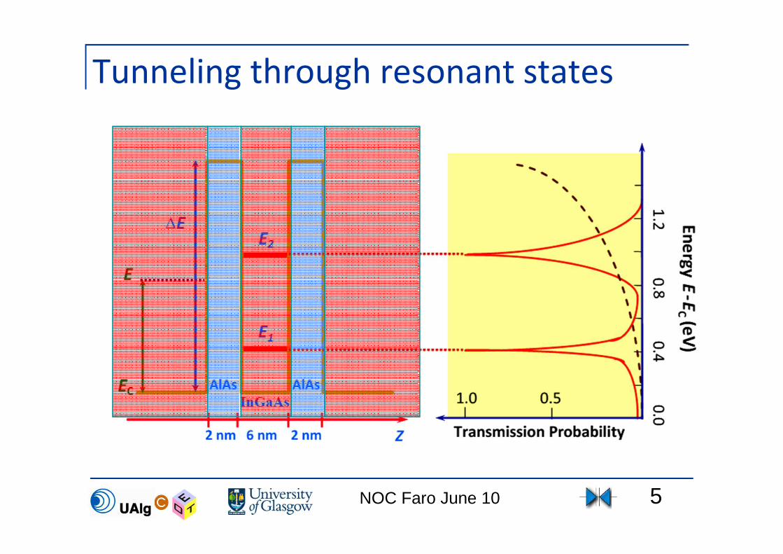
Tunneling through resonant states
5
NOC Faro June 10
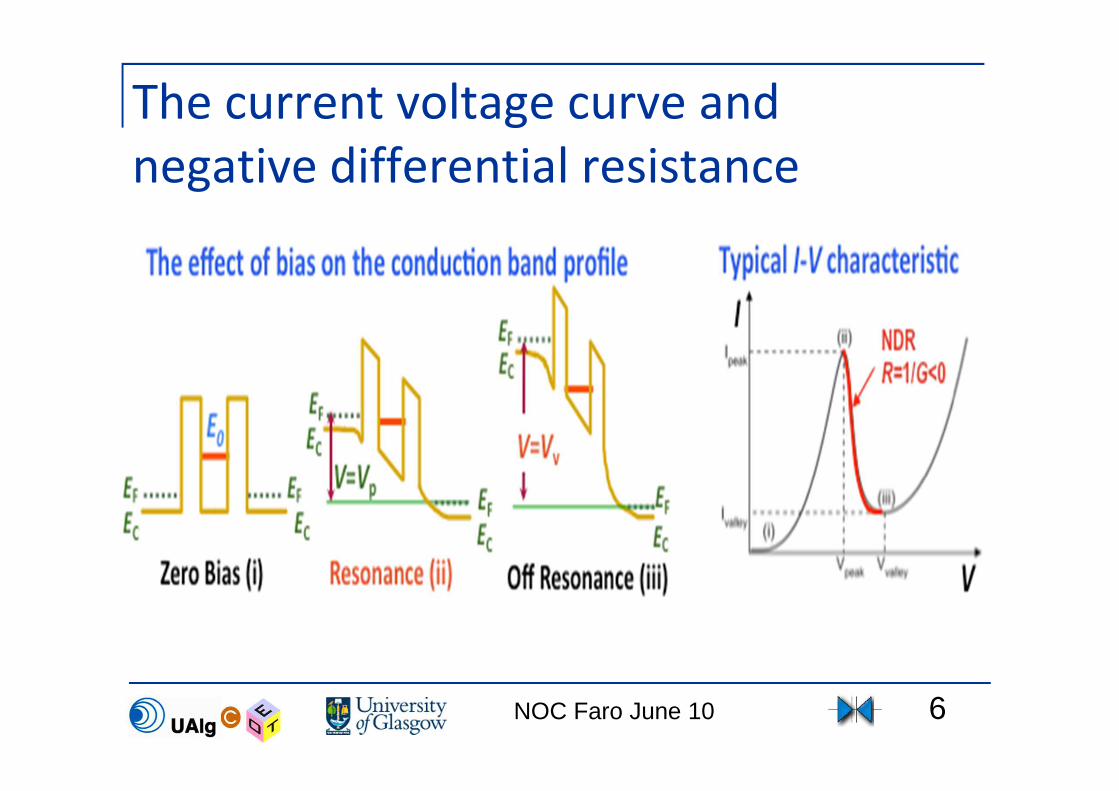
The current voltage curve and
negative differential resistance
6

NOC Faro June 10
The measured I-V curve for a RTD
7
Oscillation in the NDR region
NOC Faro June 10
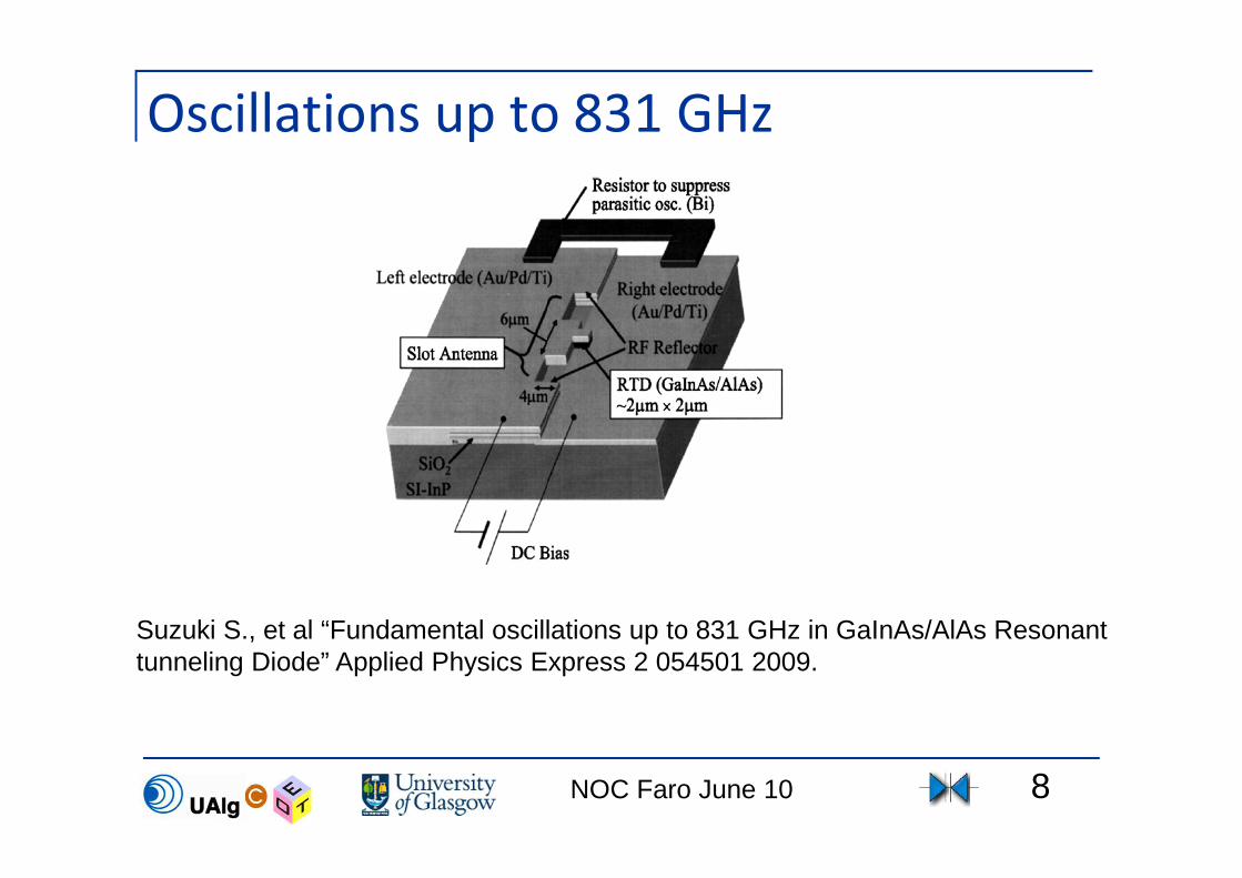
Oscillations up to 831 GHz
8
Suzuki S., et al “Fundamental oscillations up to 831 GHz in GaInAs/AlAs Resonant tunneling Diode” Applied Physics Express 2 054501 2009.
NOC Faro June 10
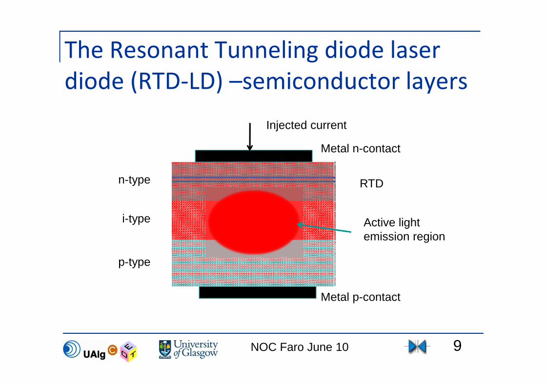
The Resonant Tunneling diode laser
diode (RTD-LD) –semiconductor layers
9
n-type
i-type
p-type
RTD
Metal n-contact
Active light emission region
Injected current
Metal p-contact
NOC Faro June 10
Layer no. Material Comp. fraction
Thickness µµµµm/ Å
Doping type
Doping conc.
Comments
Wafer InP i
1 InGaAs X=0.53 0.2µm p 5*1018cm-3 Bottom contact layer
2 InAlAs X=0.52 1 µm p 5*1017cm-3 Cladding
3 Inx Aly
Ga1-x-y As
X=0.53 Y=0.20
0.25 µm i Waveguiding core
4 Active Layer i Six quantum wells
5 Inx Aly
Ga1-x-y As
X=0.53
Y=0.20
0.25 µm i Waveguiding core
6 InAlAs X=0.52 1 µm n 5*1017cm-3 Cladding
7 InxGa1-xAs X=0.53 0.1µm n 1*1018cm-3 Laser isolation contact
8 InGaAs X=0.53 20 Å i Spacer
9 AlAs 25Å i Barrier (strained)
10 InGaAs X=0.53 50Å i Quantum well
11 AlAs 25Å i Barrier (strained)
12 InGaAs X=0.53 20A i Spacer
13 InGaAs X=0.53 0.1µm n 1*1018cm-3
14 InGaAs X=0.53 0.2µm n 5*1018cm-3 Cap layer
Quantum wells
Material Comp. fraction
Thickness Å/ ML
Doping type
Doping conc.
Comments
1 InxGa1-xAs X=0.53 67 Å i Quantum well (*6)
2 Inx Aly
Ga1-x-y As
X=0.53 Y=0.20
90 Å i Barrier (*5)
MQW Laser
RTD
LaserActive Region
10
The details of the RTD-LD Wafer
Design

NOC Faro June 10
Integrated RTD-LD Chip layout
p-type contact
n-type contact
Laser active region
RTD
Silica InsulatingLayer
3µm wide laser ridge
22µm wide ridge
Semi-insulating substrate
Heavily p-doped InGaAs
contact layer
Laseremission
11
NOC Faro June 10
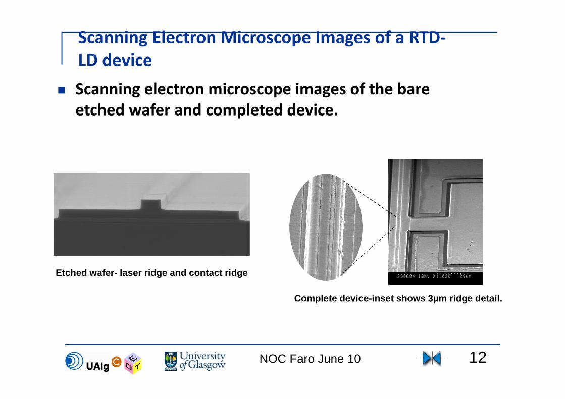
Scanning Electron Microscope Images of a RTD-
LD device
Scanning electron microscope images of the bare
etched wafer and completed device.
Etched wafer- laser ridge and contact ridge
Complete device-inset shows 3µm ridge detail.
12
NOC Faro June 10
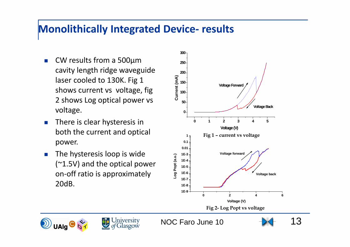
Monolithically Integrated Device- results
CW results from a 500µm
cavity length ridge waveguide
laser cooled to 130K. Fig 1
shows current vs voltage, fig
2 shows Log optical power vs
voltage.
There is clear hysteresis in
both the current and optical
power.
The hysteresis loop is wide
(~1.5V) and the optical power
on-off ratio is approximately
20dB.
0
50
100
150
200
250
300
0 1 2 3 4 5
Voltage (V)
Cur
rent
(m
A)
Voltage Forward
Voltage Back
0 2 4 61E-9
1E-8
1E-7
1E-6
1E-5
1E-4
1E-3
0.01
0.1
1
Log
Pop
t (a.
u.)
Voltage (V)
Voltage forward
Voltage back
Fig 1 – current vs voltage
Fig 2- Log Popt vs voltage
13
NOC Faro June 10
The monolithic RTD-LD ->Hybrid RTD-LD
The monolithic RTD-LD showed hysteresis –good for NRZ
operation- but no oscillation and only pulsed room
temperature operation
To gain a further insight into the operation of RTD-LD we
moved to a hybrid version – with a RTD chip and a LD
chip connected by a bond wire
The work we now present is based on the hybrid version
From this work it was clear the monolithic version had a
large series resistance probably a contact resistance –
thus heating and hysteresis
14

NOC Faro June 10
The hybrid RTD–LD
Photo-detected output
RF
outputd. c. bias
Laser Diode
Au
Printed Circuit Board
Microstrip line
Shunt
Capacitor
n
p
RTDfiber
Current-voltage (I-V) characteristics Voltage controlled oscillator
15
NOC Faro June 10
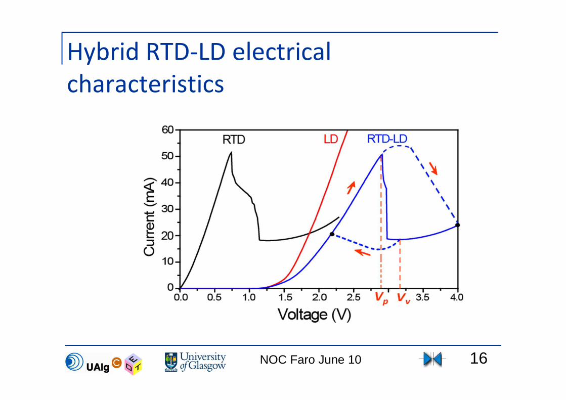
Hybrid RTD-LD electrical
characteristics
16

NOC Faro June 10
Hybrid RTD-LD Optoelectronic
oscillations
17
Electrical output
Optical output
NOC Faro June 10
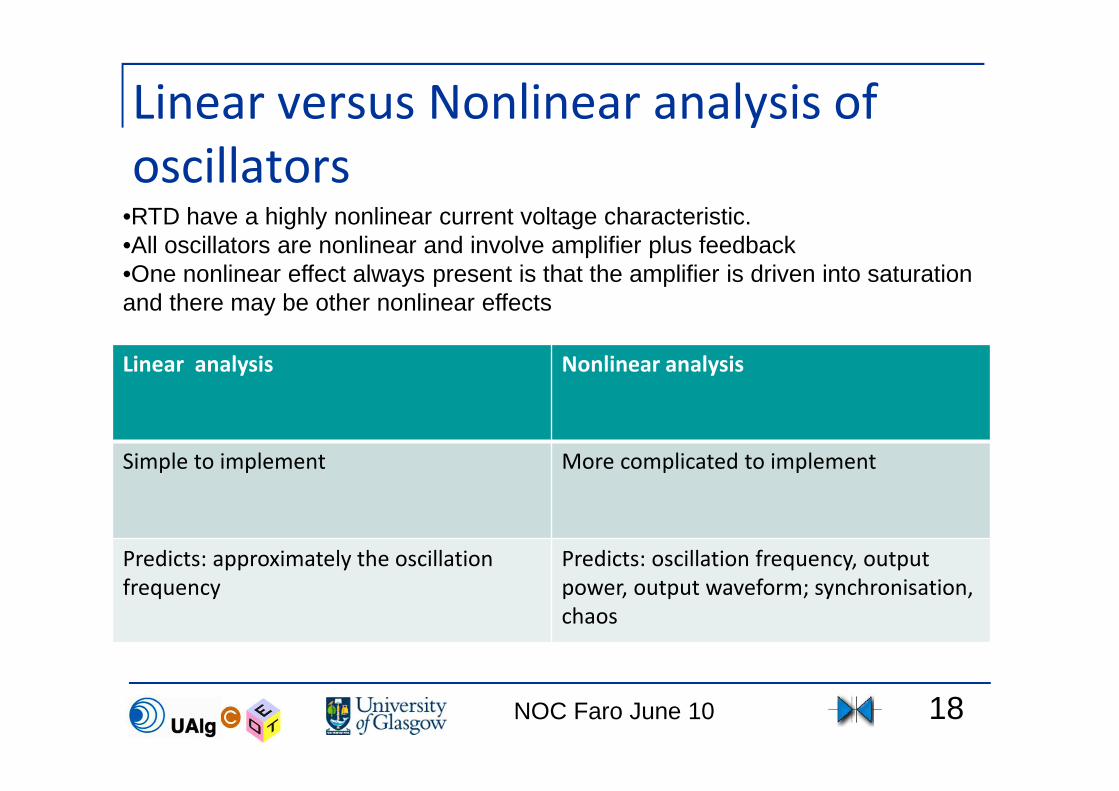
Linear versus Nonlinear analysis of
oscillators
18
•RTD have a highly nonlinear current voltage characteristic.•All oscillators are nonlinear and involve amplifier plus feedback•One nonlinear effect always present is that the amplifier is driven into saturation and there may be other nonlinear effects
Linear analysis Nonlinear analysis
Simple to implement More complicated to implement
Predicts: approximately the oscillation
frequency
Predicts: oscillation frequency, output
power, output waveform; synchronisation,
chaos

NOC Faro June 10
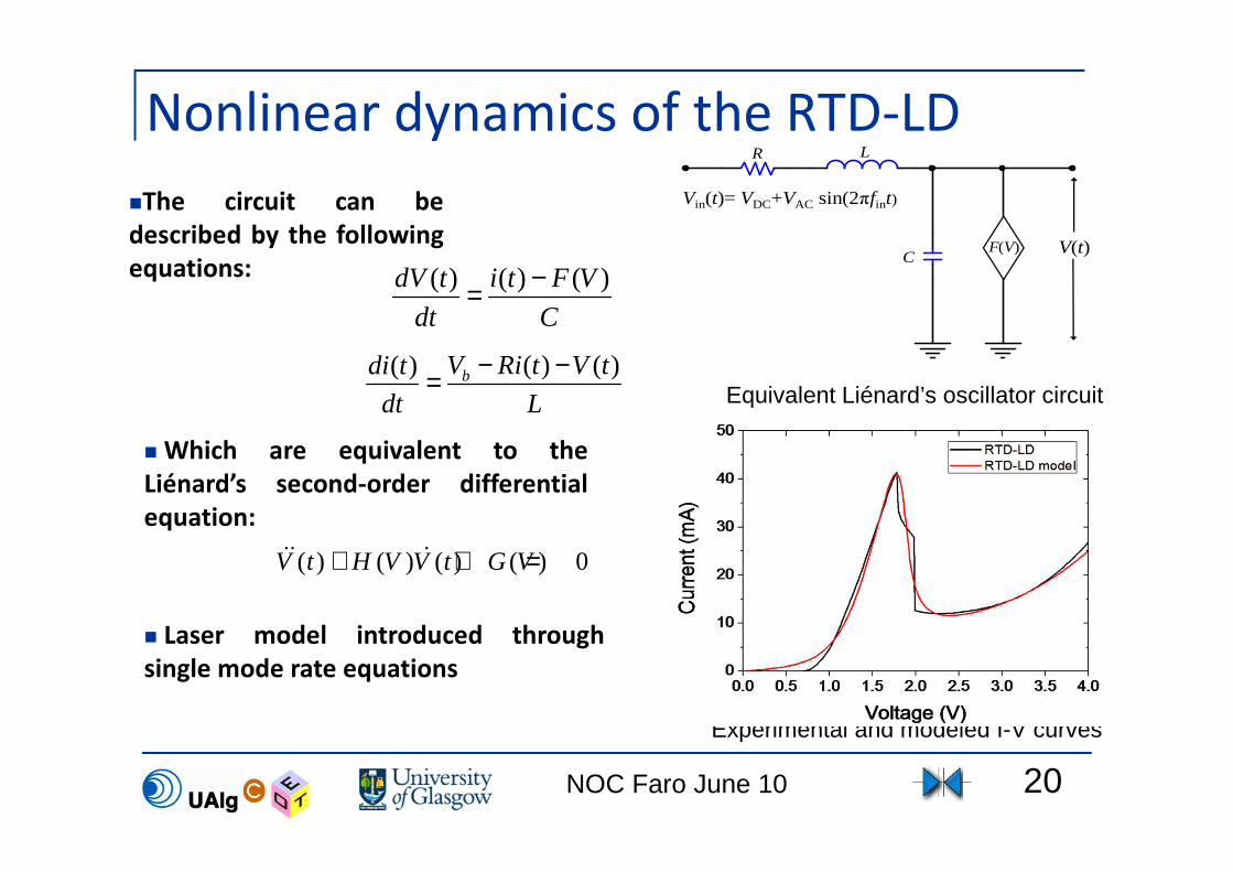
The nonlinear analysis of the RTD -
OEICs
19
•Van der Pol Oscillator had been implement before for negative differential resistance devices
•Liénard’s Oscillator is a generalisation of the The Van der Pol oscillator and allowed us to predict the Voltage frequency curve (VCO), the synchronisation and chaos behaviour
•Synchronisation is particularly important for the Wireless/Optical interface application and the operation of the RTD-LD as a Injection Locked Oscillator (ILO)
NOC Faro June 10
Experimental and modeled I-V curves
Equivalent Liénard’s oscillator circuit
F(V)C
LR
V(t)
Vin(t)= VDC+VAC sin(2πfint)
( ) ( ) ( ) ( ) 0V t H V V t G V+ + =&& &
( ) ( ) ( )dV t i t F V
dt C
−=
The circuit can be
described by the following
equations:
Which are equivalent to the
Liénard’s second-order differential
equation:
( ) ( )( ) bV Ri t V tdi t
dt L
− −=
Laser model introduced through
single mode rate equations
20
Nonlinear dynamics of the RTD-LD

NOC Faro June 10
RTD-LD The Optoelectronic Voltage Controlled Oscillator (VCO)
21
NOC Faro June 10
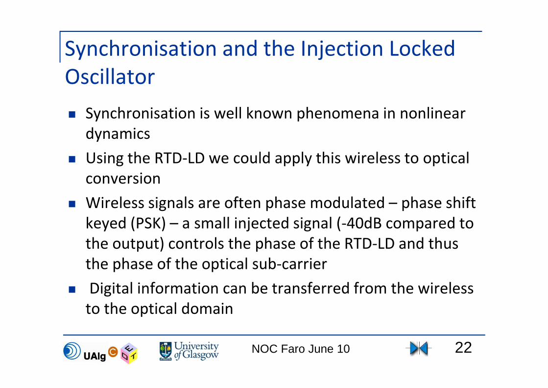
Synchronisation and the Injection Locked
Oscillator
Synchronisation is well known phenomena in nonlinear
dynamics
Using the RTD-LD we could apply this wireless to optical
conversion
Wireless signals are often phase modulated – phase shift
keyed (PSK) – a small injected signal (-40dB compared to
the output) controls the phase of the RTD-LD and thus
the phase of the optical sub-carrier
Digital information can be transferred from the wireless
to the optical domain
22
NOC Faro June 10
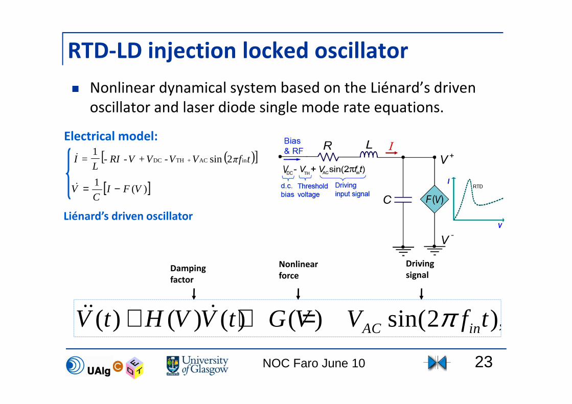
RTD-LD injection locked oscillator
Nonlinear dynamical system based on the Liénard’s driven
oscillator and laser diode single mode rate equations.
( )[ ]tfπVVVVRIL
I inAC+THDC 2sin-+--1
=&
[ ])(1
VFIC
V −=&
( ) ( ) ( ) ( ) sin(2 ),AC inV t H V V t G V V f tπ+ + =&& &
Electrical model:
Liénard’s driven oscillator
Damping
factor
Nonlinear
force
Driving
signal
23

NOC Faro June 10
Injection locking Experimental synchronization in the laser output
Fundamental Second harmonic
24

NOC Faro June 10
Liénard’s RTD-LD 2D Synchronization Map
fin/3
fin/4
RTD-LD frequency locking structure showing the Arnold Tongues map: a comparison of theory with experimental results
fin/1
fin/2
fin/3
fin/4 fin/1 - when the injected
wireless signal is at the same frequency as the natural oscillation frequency
fin/2 - when the injected wireless signal is twice the frequency of the natural oscillation
The y axis is the amplitude of the injected wireless signal
fin/1 fin/2 fin/3
25

NOC Faro June 10
Adler’s equation – the short version of
Arnold’s tongues
0
0
2=∆
P
P
Q
ff
inj
factorquality oscillator -Q
oscillator ofpower output -P
signal injected ofpower P
frequency oscillator f
range locking∆f
0
inj
0
−−−
26
NOC Faro June 10
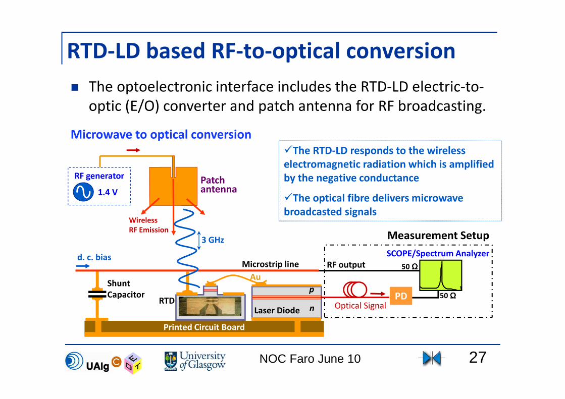
RTD-LD based RF-to-optical conversion
The optoelectronic interface includes the RTD-LD electric-to-
optic (E/O) converter and patch antenna for RF broadcasting.
3 GHz
Patch antenna
RF output
Laser Diode
Au
Printed Circuit Board
Microstrip line
Shunt
Capacitor
n
p
RTD
d. c. bias
The RTD-LD responds to the wireless
electromagnetic radiation which is amplified
by the negative conductance
The optical fibre delivers microwave
broadcasted signals
Microwave to optical conversion
Wireless
RF Emission
Optical Signal
Measurement Setup
SCOPE/Spectrum Analyzer
PD
RF generator
50 ΩΩΩΩ
1.4 V
50 ΩΩΩΩ
27

NOC Faro June 10
Analogue Phase Modulation The laser diode output, locked with a broadcasted signal, shows the
same modulation features of the injected signal with the same
sidebands at 1 MHz offset of the radio frequency sub-carrier.
Most digital wireless signals are phase shift keyed (PSK) and so, because of the
fixed phase relationship, the phase synchronization of the RTD-LD can be used to
translate the digital information from the wireless to the optical domain.
28
NOC Faro June 10
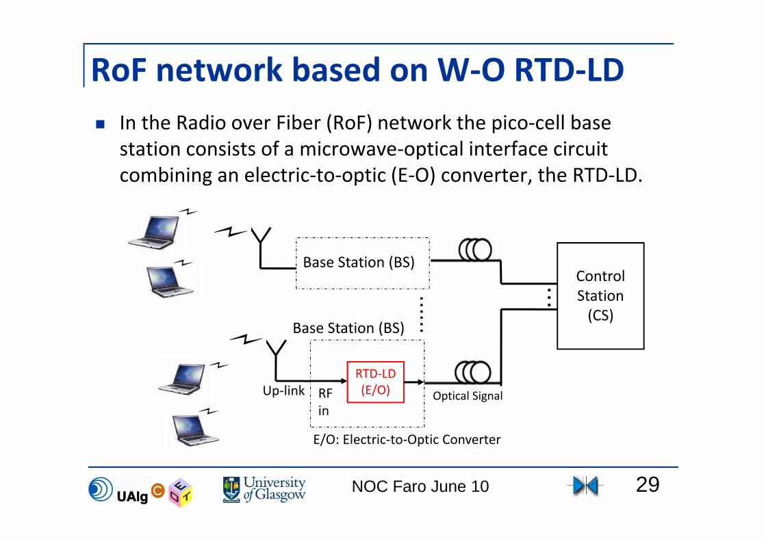
RoF network based on W-O RTD-LD
In the Radio over Fiber (RoF) network the pico-cell base
station consists of a microwave-optical interface circuit
combining an electric-to-optic (E-O) converter, the RTD-LD.
Base Station (BS)
RTD-LD
(E/O)
Control
Station
(CS)
E/O: Electric-to-Optic Converter
Optical Signal
Base Station (BS)
RF
in
Up-link
29
NOC Faro June 10
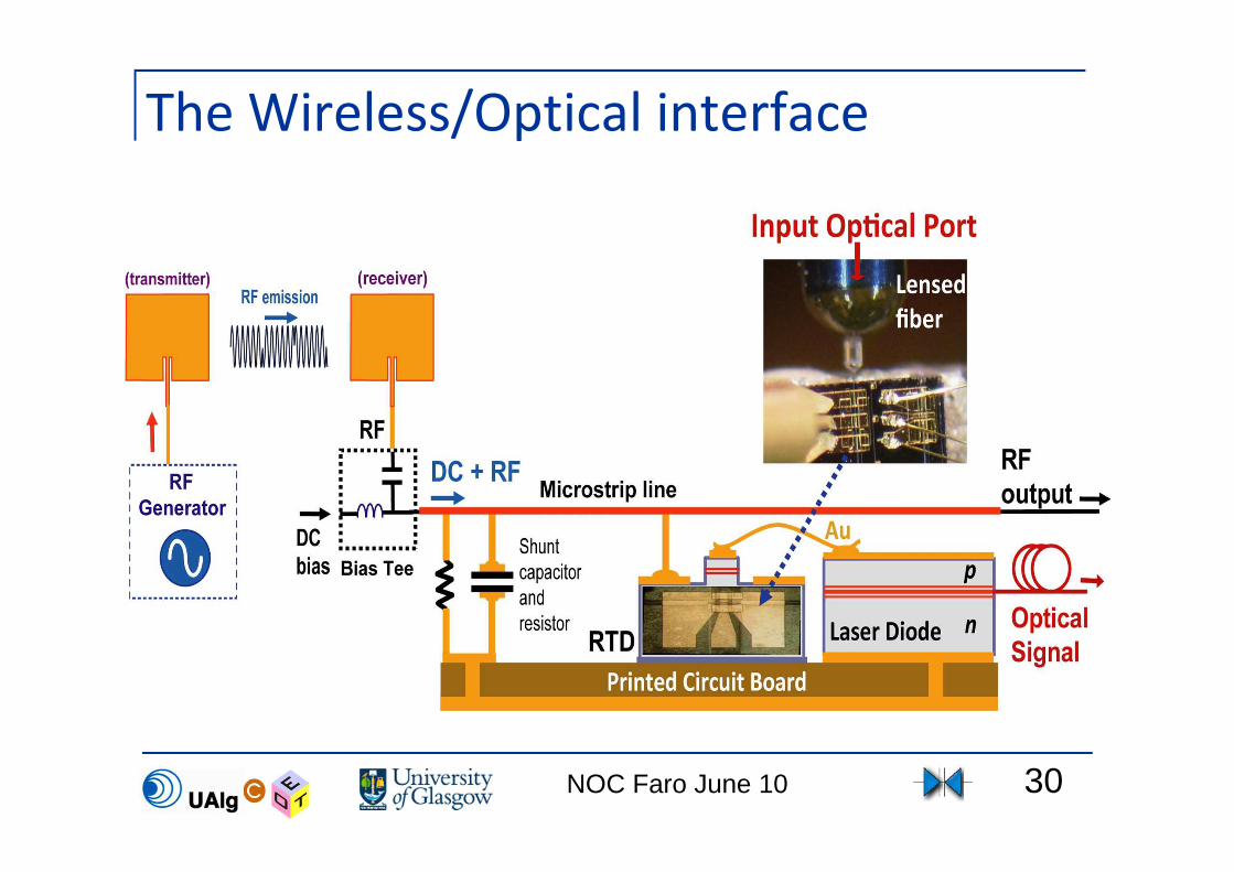
The Wireless/Optical interface
30
NOC Faro June 10
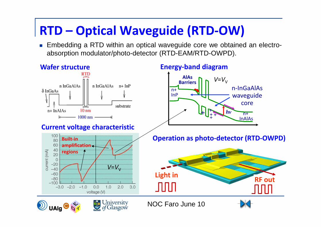
RTD – Optical Waveguide (RTD-OW) Embedding a RTD within an optical waveguide core we obtained an electro-
absorption modulator/photo-detector (RTD-EAM/RTD-OWPD).
Wafer structure
Operation as photo-detector (RTD-OWPD)
Current voltage characteristic
+ + +++
hv
n-InGaAlAswaveguide
core
n+ InAlAs
AlAsBarriers
Energy-band diagram
n+ InP
V=VV
V=VV
RF inLight in
RF out
Built-in
amplification
regions
NOC Faro June 10
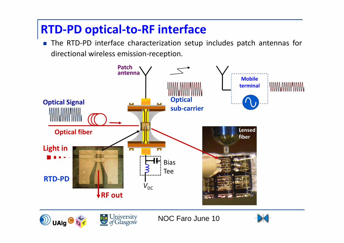
RTD-PD optical-to-RF interface The RTD-PD interface characterization setup includes patch antennas for
directional wireless emission-reception.
Patch antenna
Optical Signal
Bias
Tee
Mobile
terminal
RTD-PD VDC
Optical fiber
Optical
sub-carrier
Light in
RF out
Lensed
fiber
NOC Faro June 10
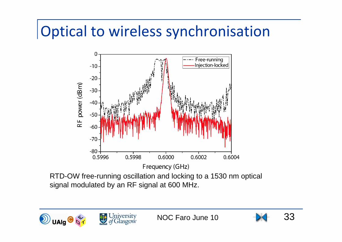
Optical to wireless synchronisation
33
RTD-OW free-running oscillation and locking to a 1530 nm opticalsignal modulated by an RF signal at 600 MHz.

NOC Faro June 10
The driven RTD-LD – chaos generation
34
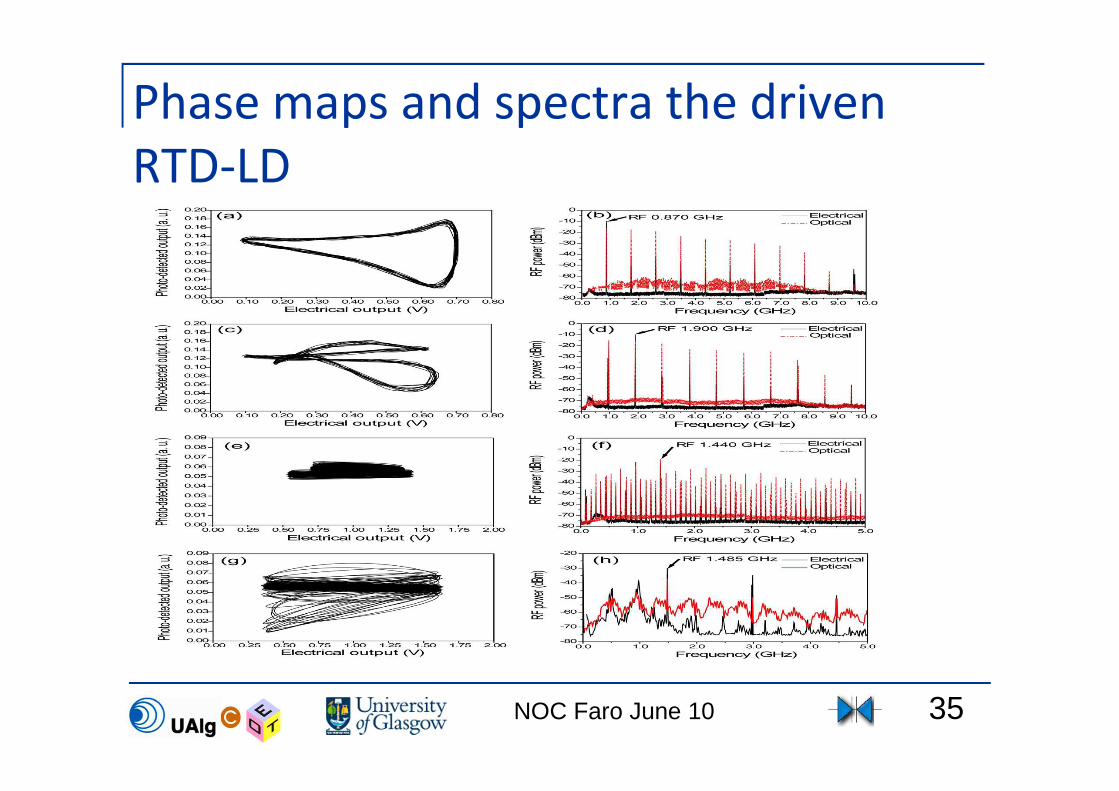
NOC Faro June 10
Phase maps and spectra the driven
RTD-LD
35

NOC Faro June 10
Steganography –camouflage for
signals –just add chaos.
36
•At source chaos generator is modulated but chaos >modulation so signal looks like noise
•Deterministic chaos can be removed by receiver and signal recovered

NOC Faro June 10
Summary and Conclusion
Introduction to the RTD the fastest electronic device
The RTD-LD can be monolithically integrated
The hybrid RTD-LD has allowed as to verify the Lienard’s oscillator model
Modulation of the phase of the radio frequency sub-carrier was demonstrated in
the laser output.
First demonstration of wireless to optical conversion and optical to wireless with
the RTD-PD - using synchronization of a nonlinear oscillator.
Chaos generation
37
http://userweb.elec.gla.ac.uk/i/ironside/RTD/RTDOpto.html


![UNIVERSITY OF CALIFORNIA Santa Barbara Heterogeneous ... · laser in a coupled optoelectronic oscillator configuration," in CLEO: 2013, San Jose, California, p. CTu2G.2. [17] S. Srinivasan](https://img.pdfslide.net/doc/110x75/60394a53ae75fb034c2e017a/university-of-california-santa-barbara-heterogeneous-laser-in-a-coupled-optoelectronic.jpg)