Embed Size (px)
Citation preview
Nano Trends: A Journal of Nanotechnology and its Applications
Volume 1, Issue 1, July 2006, Pages 27-42.
-------------------------------------------------------------------------------------------------------
ISSN 0973-418X © NSTC 2006. All Rights Reserved.
27
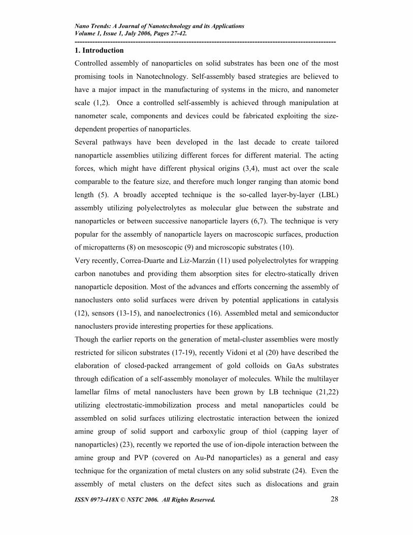
Ordered Assembly of Pd Nanoparticles on Electronic Substrates
U. Pal
1*, and M. Herrera-Zaldívar
2
1Instituto de Física, Universidad Autónoma de Puebla, Apdo. Postal J-48, Puebla,
Pue. 72570, Mexico. E-mail: [email protected] 2Centro de Ciencias de la Materia Condensada, Universidad Nacional Autónoma de
México, Apdo. Postal 2681, Ensenada, BC 22800, Mexico. E-mail:
PACS: 81.07.Bc, 81.16.Dn, 81.16.Rf, 81.20.Ka, 68.37.Ef
Abstract
Room temperature assembly of Pd nanoparticles on solid electronic substrates like Si,
SiC and C are studied. A one-step chemical reduction method without any surfactant
or functionalizing agent was used. The Pd nanoparticles of different average sizes
could be nucleated and grown in well-organized manner over a large area of C and C-
terminated SiC substrates, while the nanoparticles formed on Si or Si-terminated SiC
substrates did not organize well. By controlling the process parameters, the average
diameter of the Pd nanoparticles could be controlled. It is found that the unsaturated C
bonds on the substrate surface play the main role for organizing Pd nanoparticles on
them. The Pd nanoparticles on the solid substrates are well crystalline and retain their
bulk crystal structure.
Short Title: Assembly of Pd nanoparticles ________________________________________________________________ *Corresponding author, Fax: +52-222-2295611
Nano Trends: A Journal of Nanotechnology and its Applications
Volume 1, Issue 1, July 2006, Pages 27-42.
-------------------------------------------------------------------------------------------------------
ISSN 0973-418X © NSTC 2006. All Rights Reserved.
28
1. Introduction
Controlled assembly of nanoparticles on solid substrates has been one of the most
promising tools in Nanotechnology. Self-assembly based strategies are believed to
have a major impact in the manufacturing of systems in the micro, and nanometer
scale (1,2). Once a controlled self-assembly is achieved through manipulation at
nanometer scale, components and devices could be fabricated exploiting the size-
dependent properties of nanoparticles.
Several pathways have been developed in the last decade to create tailored
nanoparticle assemblies utilizing different forces for different material. The acting
forces, which might have different physical origins (3,4), must act over the scale
comparable to the feature size, and therefore much longer ranging than atomic bond
length (5). A broadly accepted technique is the so-called layer-by-layer (LBL)
assembly utilizing polyelectrolytes as molecular glue between the substrate and
nanoparticles or between successive nanoparticle layers (6,7). The technique is very
popular for the assembly of nanoparticle layers on macroscopic surfaces, production
of micropatterns (8) on mesoscopic (9) and microscopic substrates (10).
Very recently, Correa-Duarte and Liz-Marzán (11) used polyelectrolytes for wrapping
carbon nanotubes and providing them absorption sites for electro-statically driven
nanoparticle deposition. Most of the advances and efforts concerning the assembly of
nanoclusters onto solid surfaces were driven by potential applications in catalysis
(12), sensors (13-15), and nanoelectronics (16). Assembled metal and semiconductor
nanoclusters provide interesting properties for these applications.
Though the earlier reports on the generation of metal-cluster assemblies were mostly
restricted for silicon substrates (17-19), recently Vidoni et al (20) have described the
elaboration of closed-packed arrangement of gold colloids on GaAs substrates
through edification of a self-assembly monolayer of molecules. While the multilayer
lamellar films of metal nanoclusters have been grown by LB technique (21,22)
utilizing electrostatic-immobilization process and metal nanoparticles could be
assembled on solid surfaces utilizing electrostatic interaction between the ionized
amine group of solid support and carboxylic group of thiol (capping layer of
nanoparticles) (23), recently we reported the use of ion-dipole interaction between the
amine group and PVP (covered on Au-Pd nanoparticles) as a general and easy
technique for the organization of metal clusters on any solid substrate (24). Even the
assembly of metal clusters on the defect sites such as dislocations and grain
Nano Trends: A Journal of Nanotechnology and its Applications
Volume 1, Issue 1, July 2006, Pages 27-42.
-------------------------------------------------------------------------------------------------------
ISSN 0973-418X © NSTC 2006. All Rights Reserved.
29
boundaries of solid electronic substrates has been studied for quite a long time [25-
28], recent prospect of versatile applications of nanocluster assemblies generated a
huge thrust for their uniform 2-D assemblies on solid substrates. In ex-situ processes,
apart from the defect site induced assemblies, carboxylic acid, or amine groups are
being used to produce self-assembled nanoparticles on solid substrates. Although, for
catalytic and biological applications, use of such organic substances may not have any
adverse effect on the performance of the assemblies, for electronic applications they
are bound to affect device performance.
In the present study we tried to fabricate Pd nanocluster assemblies on several
electronic substrates like C, SiC and Si without using any capping agent either on the
metal clusters or on the substrates. By chemical reduction of the Pd ions in a
methanolic solution in presence of solid electronic substrates, site selective assemblies
of Pd nanoclusters could be fabricated over C-terminated SiC layers and amorphous C
substrates. The nanoparticle assemblies were studied by SEM, EDS and STM
techniques. Nucleation and growth of Pd clusters at the unsaturated c-sites are
proposed as the mechanism for their assembled growth on the C-terminated SiC and
amorphous C substrates.
2. Experimental
Pd nanoparticles on different substrates like SiC and carbon were grown by reducing
the palladium metal ions on the substrate surfaces. In a typical synthesis process,
either of the solid substrates such as SiC (6H) wafer (epitaxially grown, CREE
H0124-15), SiC (4H) wafer (Epitaxially grown, CREE E0319-3), amorphous carbon
(carbon coated microscopic grids, Nissin EM Co., LTD.) and Si (100) (Crysteco
1702-3) was immersed into 10 ml methanolic solution of PdCl2 (Alfa Aesar, 99.9%;
0.033 mmol/50 ml of methanol) under mild agitation. Then about 0.5 ml of aqueous
solution of NaBH4 (0.044 M) was added to it drop-wise. After the addition of the
reductor (NaBH4 solution), the substrate was removed from the solution at different
intervals of time. The substrates were then rinsed in methanol and dried in air at room
temperature. Typical size of the SiC (6H), SiC (4H) and Si (100) wafers used as
substrates was of about 5 mm x 5 mm, while the size of the C-coated copper grids was
3 mm diameter.
A JEOL JSM5300 scanning electron microscope (SEM), attached with a Thermo
Noran Super-dry II energy dispersive X-ray spectrometer (EDS) was used for the
Nano Trends: A Journal of Nanotechnology and its Applications
Volume 1, Issue 1, July 2006, Pages 27-42.
-------------------------------------------------------------------------------------------------------
ISSN 0973-418X © NSTC 2006. All Rights Reserved.
30
morphology and composition analysis of the samples. A NanoScope E STM (Digital
Instruments) operated in ambient condition was employed for the topographic
characterizations. All the STM images presented in this work were taken in constant
current (topographical) mode, using electrochemically etched W wires as probe-tips.
For scanning tunnelling spectroscopy (STS), mechanically sharpened Pt-Ir wires were
used as tips. I-V data were collected following a common procedure: the feedback
loop of the microscope that controls the vertical motion of the tip was interrupted
momentarily and the bias voltage was digitally ramped from an initial to a final pre-
selected value, while the corresponding tunnel current was digitally sampled.
3. Results and Discussion
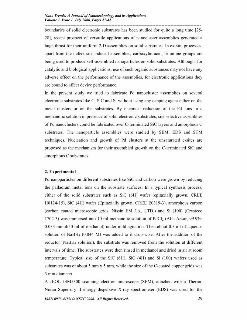
Figure 1 shows the SEM images of the Pd clusters deposited over Si substrate at
different times of immersion. We can observe the formation of nanoclusters over the
substrate in unassembled manner. While for 5 min of immersion, the clusters
remained well dispersed over the substrate, for longer time of immersion more
clusters were formed and aggregated to form bigger clusters. Formation of Pd clusters
on Si substrate in irregular manner indicates that the initial nucleations occurred at the
defect sites such as dislocations of the substrate. On longer time of immersion, more
Pd clusters are formed in the reaction solution and aggregated to the initial clusters on
the substrate.
Nano Trends: A Journal of Nanotechnology and its Applications
Volume 1, Issue 1, July 2006, Pages 27-42.
-------------------------------------------------------------------------------------------------------
ISSN 0973-418X © NSTC 2006. All Rights Reserved.
31
Figure 1 - Typical SEM images of Pd clusters deposited over Si substrate for a) 5
min, and b-c) 15 min of immersion in the reaction solution. The scale bars
in a), b), and c) are 100, 100 and 40 µm respectively.
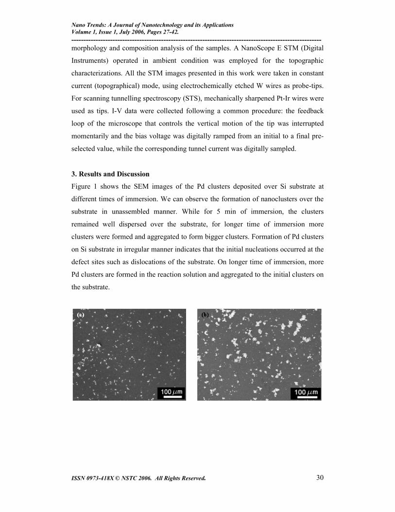
The formation pattern of Pd clusters on Si-terminated SiC (4H) substrate is quite
similar to that of Si substrate. In figure 2, the SEM micrographs of the Pd cluster
deposited Si-terminated SiC substrate are presented.
Figure 2 - Typical SEM images of Pd clusters deposited over Si-terminated SiC
substrate for a) 5 min, and b) 15 min of immersions in the reaction
solution. The scale bars in a) and b) are 100 µm and 800 nm
respectively.
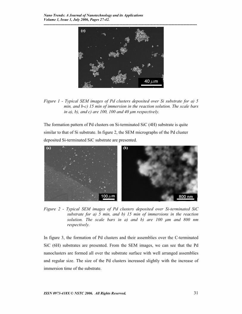
In figure 3, the formation of Pd clusters and their assemblies over the C-terminated
SiC (6H) substrates are presented. From the SEM images, we can see that the Pd
nanoclusters are formed all over the substrate surface with well arranged assemblies
and regular size. The size of the Pd clusters increased slightly with the increase of
immersion time of the substrate.

Nano Trends: A Journal of Nanotechnology and its Applications
Volume 1, Issue 1, July 2006, Pages 27-42.
-------------------------------------------------------------------------------------------------------
ISSN 0973-418X © NSTC 2006. All Rights Reserved.
32
Figure 3 - Typical SEM images of the Pd clusters formed over C-terminated SiC
substrate for a) 2 min, b) 5 min, and c) 20 min of immersions in the
reaction solution.
The formation and assembly of Pd nanoclusters over C-coated Cu grids are shown in
figure 4. With the increase of immersion time the clusters grown bigger, and for
longer immersion times, some agglomerated structures are formed over the surface. It
should be noted that the carbon coating over the microscopic grid was of amorphous
nature. Formation of well-ordered assembly of Pd clusters over the C-terminated SiC
and amorphous carbon layers, in contrast to the irregular features over Si-terminates
SiC surface clearly indicates the role of C on the ordered assembly of the clusters. We
believe the C at the surface of the C-terminated SiC and amorphous C films remain
unsaturated, forming dangling bonds which act as the nucleation centers for the
formation of Pd clusters. Recently a few reports have been published on the assembly
of metal clusters over carbon nanotubes without using organic functionalizing agents.
Though by controlling the hydrophilicity of CNTs, it is possible to fabricate metal or
semiconductor cluster-assemblies over them by proper choice of capping agents over
the clusters (11,29), without organic capping agent, metal clusters do not assemble

Nano Trends: A Journal of Nanotechnology and its Applications
Volume 1, Issue 1, July 2006, Pages 27-42.
-------------------------------------------------------------------------------------------------------
ISSN 0973-418X © NSTC 2006. All Rights Reserved.
33
over the carbon surface. Satishkumar et al. (30) were successful to decorate CNTs by
Au, Pt and Ag clusters through nitric acid refluxing. By nitric acid refluxing, they
generated acid sites over the nanotube surfaces which acted as nucleation centers.
Though by controlling the concentration of the metal ions they could control the
surface coverage of metal clusters over the CNT surface, the metal clusters did not
form ordered assemblies. In our case, as the whole surfaces of the C-terminated SiC
and C-coatings over the microscopic grids were covered with C-sites with dangling
bonds, the metal clusters could be assembled in well ordered manner.
Figure 4 - Typical SEM images of the Pd cluster assemblies formed over amorphous
carbon surface for a) 5 min, b) 10 min, and c) 20 min of immersion times.
The use of methanol as the solvent for reducing noble metal ions in is well established
(31, 32). On addition of freshly prepared NaBH4 aqueous solution results the
reduction of metal ions following the equation:
4Mn+ + nBH4- + 3nH2O 4M0 + nH2BO3
- + 4nH+ + 2nH2
The presence of Pd in the clusters could be verified from the EDS spectra of the
samples. In figure 5, a typical EDS spectrum of the clusters formed over C-coated Cu
grid is shown. While the Cu and C peaks appeared in the spectrum from the C-coated

Nano Trends: A Journal of Nanotechnology and its Applications
Volume 1, Issue 1, July 2006, Pages 27-42.
-------------------------------------------------------------------------------------------------------
ISSN 0973-418X © NSTC 2006. All Rights Reserved.
34
Cu grids, the Al and O peaks appeared from the Al substrate holder of the
microscope. Absence of chlorine peak in the EDS spectrum indicates its complete
removal from the sample after washing.
Figure 5 - Typical EDS spectrum of Pd nanoclusters assembled over C substrate. The
sample was prepared by immersing the substrate for 20 min in the
reaction mixture. The Cu and C peaks appeared from the C-coated Cu
grid. The Al and O peaks appeared from the Al sample holder of the
microscope.
To observe the formation and characteristic features of the Pd clusters in details, the
samples were observed in STM. The C-terminated SiC substrates revealed the
formation of nanometric spherical Pd nanoparticles inside the clusters. The average
size of the nanoparticles increased from 13 nm to 20 nm on increasing the immersion
time from 2 min to 10 min (Figs. 6a-6c). However, for even longer immersion time,
the particles did not grow further, but coalesce to form interconnected structures (Fig.
6d).
0 1 2 3 4 5 60
100
200
300
Real time: 502.1
Live time: 500.0
Cu
PdPd
PdAl
Cu
O
C
Counts
X-Ray Energy (eV)

Nano Trends: A Journal of Nanotechnology and its Applications
Volume 1, Issue 1, July 2006, Pages 27-42.
-------------------------------------------------------------------------------------------------------
ISSN 0973-418X © NSTC 2006. All Rights Reserved.
35
Figure 6 - Typical STM images of the Pd nanoparticles inside of clusters grown over
C-terminated SiC substrate for a) 2 min, b) 5 min, c) 10 min, and d) 20
min of immersion in the reaction solution.
For the Pd/C sample, however, the Pd nanoparticles were grown with considerably
smaller in size. The average size of the particles varied from 8 nm to 10 nm for the
increase of immersion time from 5 min to 20 min (Fig. 7). Moreover, on increasing
the immersion time further, the particles did not coalesce much as in case of C-
terminated SiC substrates.
We believe the differences in the cluster size between the C-terminated SiC and
amorphous carbon substrates might be due to the influence of the dangling bond
concentration of the substrates that act as nucleation centers. For amorphous carbon,
sp2 bondings have been proposed to explain the formation of chains and connections
between the disordered regions (33), which reduce the tetrahedral sp3 coordinations.
A higher amount of tetrahedral sp3 dangling bonds in the crystalline SiC are exposed
over the C-terminated SiC surface (34-36) which acts as Pd nucleation centers.
Presence of sp3 dangling bonds in higher concentration in the latter case produces
dense, compact Pd cluster assemblies as revealed from the SEM images (Figs. 3 and
4) than the earlier. Moreover, this may be a reason for the higher average size of the
Pd particles formed over C-terminated SiC substrate than over amorphous carbon for
a similar interval of immersion time. For longer time of immersion, while the
40nm 40nm
40nm 40nm
a b
c d
40nm 40nm
40nm 40nm
a b
c d

Nano Trends: A Journal of Nanotechnology and its Applications
Volume 1, Issue 1, July 2006, Pages 27-42.
-------------------------------------------------------------------------------------------------------
ISSN 0973-418X © NSTC 2006. All Rights Reserved.
36
nanoparticles formed over amorphous carbon substrate continue to grow without
coalescence, the nanoparticles over C-terminated SiC substrates stop growing after
about 10 min and coalesce for longer immersion time.
Figure 7 - Typical STM images of the Pd nanoparticles grown over amorphous
carbon substrates for a-b) 5 min, c) 10 min, and d) 20 min of immersion
in the reaction solution.
Figure 8 shows the representative I-V curves for the Pd particles over carbon and C-
terminated SiC substrates. The spectra were recorded putting the tips on isolated Pd
particles in both the cases and with the same tip-sample separation. At low voltages,
where the tunnel current depends exponentially on the tip-sample separation and
surface states density [37], similar values for the tunnel current are observed, and
therefore, analogous electronic properties are expected for the Pd nanoparticles in
both the samples. At higher voltages, while the Pd nanoparticle over carbon substrate
revealed metallic behavior (linear variation of tunneling current), the Pd nanoparticle
over SiC revealed non-metallic characteristics. It must be noted that while the carbon
substrate we used was electronically of metallic nature, the SiC was a semiconductor
with high band gap. It is well known that the tunneling spectra recorded above the
supported nanoparticles exhibit chemical states of both the particles and the particle-
support (38-41). The linear variation of tunneling current in the case of Pd particles on
carbon support indicates that our Pd particles are clean. As all the samples were
grown at the same experimental conditions, we believe, the Pd nanoparticles over SiC
10nm20nm
10nm 10nm
a b
c d
10nm20nm
10nm 10nm
a b
c d

Nano Trends: A Journal of Nanotechnology and its Applications
Volume 1, Issue 1, July 2006, Pages 27-42.
-------------------------------------------------------------------------------------------------------
ISSN 0973-418X © NSTC 2006. All Rights Reserved.
37
substrates are also clean. Therefore, the non-metallic I-V spectrum for the Pd particles
over SiC must be due to the interfacial electronic or chemical states between the Pd
particle and the substrate, which is not surprising due to semiconducting nature of
SiC.
Figure 8 - I-V spectra obtained at 1.2 nA and 50 meV for Pd nanoparticles assembled
on (1) amorphous C and (2) C - terminated SiC.
Through atomic resolution STM imaging, we could see that on coalescence, the
particles form terraces (Fig. 9). Also both the particles and the terraces are well
crystalline. The lattice constant measured (a = b = 2.8 Å) from the images agree well
with the bulk lattice constant (a = b = 3.0 Å) of hexagonal Pd. So, the nanoparticles
retain their bulk crystalline structure while being assembled on the substrates.
-1000 -500 0 500 1000-100-80-60-40-200
20406080
100
1
2
I (nA)
Sampling voltage (mV)

Nano Trends: A Journal of Nanotechnology and its Applications
Volume 1, Issue 1, July 2006, Pages 27-42.
-------------------------------------------------------------------------------------------------------
ISSN 0973-418X © NSTC 2006. All Rights Reserved.
38
Figure 9 - STM images acquired at 14 mV and 5.6 nA, exhibiting (a) terraces
formation during the coalescence of Pd nanoparticles (arrows). (b)
Details of the terraces that indicate their hexagonal structure. The labels
1, 2, and 3 in (a) indicate the nanoparticles that participate in the
coalescence process.
4. Conclusions
Using a single step chemical technique, ordered-assembly of Pd nanoclusters could be
fabricated over C-terminated SiC and amorphous C substrates at room temperature.
The size of the metal clusters could be controlled simply by adjusting the immersion
time of the substrates in the reaction solution. Sp3 dangling bonds of carbon on the
substrate surfaces are assumed to be responsible for the nucleation and growth of Pd
nanoclusters. The assembled Pd clusters are consisting of several nanoparticles and
relatively free from contaminations. The Pd clusters are metallic in nature and
preserve their bulk crystalline structure while assembled over the electronic
substrates. The clusters formed over C-terminated SiC substrates reveal particle-
substrate interfacial states in their STS spectra. Using our technique, ordered
assembly of other noble metals like Pt, Au, etc. can be prepared over electronic
substrates without using any external functionalizing agent.
Nano Trends: A Journal of Nanotechnology and its Applications
Volume 1, Issue 1, July 2006, Pages 27-42.
-------------------------------------------------------------------------------------------------------
ISSN 0973-418X © NSTC 2006. All Rights Reserved.
39
Acknowledgements
We are grateful to Dr. Valenzuela-Benavides for his help in the STM image
acquisition. To Israel Gradilla for his technical help in taking SEM images of the
samples. We acknowledge the partial financial helps of CONACyT, VIEP-BUAP, and
PAPIIT-UNAM, Mexico, for partial financial helps through Grants No. 46269,
11/I/EXC/05 and IN113303, respectively.
Nano Trends: A Journal of Nanotechnology and its Applications
Volume 1, Issue 1, July 2006, Pages 27-42.
-------------------------------------------------------------------------------------------------------
ISSN 0973-418X © NSTC 2006. All Rights Reserved.
40
References
1. Fendler J. H. Chemistry of Materials 2001. 13. 3196 p.
2. Whitesides G. M. and Grybowski B. Science 2002. 295. 2418 p.
3. Murray C. B. Kagan C. R. and Bawendi M. G. Annual Review of Materials
Science 2000. 30. 545 p.
4. Suo Z. International Journals of Solids and Structures 2000. 37. 367 p.
5. Suo Z. and Lu W. Journal of Nanoparticle Research 2000. 2. 333 p.
6. Decher D. Science 1997. 277. 1232 p.
7. Kotov N. A. Dekany I. and Fendler J. H. Journal of Physical Chemistry 1996.
99. 13065 p.
8. Hammond P. T. Advanced Material 2004. 16. 1271 p.
9. Crips M. T. and Kotov N.A. Nano Letters 3. 3. 173 p.
10. Caruso F. Caruso R. A. and Möhwald H. Science 1998. 282. 1111 p.
11. Correa-Duarte M. A. and Liz-Marzán L. M. Journal of Material Chemistry
2006. 16. 22 p.
12. Grisel R. Weststrate K. J. Gluhoi A. and Nieuwenhuys B. E. Gold Bulletin
2002. 35. 39 p.
13. Nayral C. Viala E. Fau P. Senocq F. Jumas, J. C. Maisonnat A. and Chaudret
B. Chemistry – A European Journal 2000. 22. 4082 p.
14. Jitianu A. Altindag Y. Zaharescu M. and Wark M. Journal of Sol-Gel Sciience
2003. 26. 483 p.
15. Jia J. Wang B. Wu A. Cheng G. Li Z. and Dong S. Analytical Chemistry 2002.
74. 2271 p.
16. Fendler J. Chemistry of Materials 2001. 13. 3196 p.
17. Bethell D. Brust M. Schiffrin D. J. and Kiely C. J. Electroanalytical Chemistry
1996. 409. 137 p.
18. Liu S. Zhu T. Hu R. and Liu Z. Physical Chemistry Chemical Physics 2002. 4.
6059 p.
19. Snow A. W. Ancona M. G. Kruppa W. Jernigan G. Foos E. and Park D.
Journal of Material Chemistry 2002. 12. 1222 p.
20. Vidoni O. Neumeier S. Bardou N. Pelouard Jean-Luc and Schmid G. Journal
Cluster Science 2003. 14. 325 p.
Nano Trends: A Journal of Nanotechnology and its Applications
Volume 1, Issue 1, July 2006, Pages 27-42.
-------------------------------------------------------------------------------------------------------
ISSN 0973-418X © NSTC 2006. All Rights Reserved.
41
21. Sastry M. Mayya K. S. Patil V. Paranjape D. V. Hegre S. G. Journal of
Physical Chemistry B 1997. 101. 4954 p.
22. Bardosova M. Tredgold R. H. Ali-Adib Z. Langmuir 1995. 11. 1273 p.
23. Mayya K. S. Patil V. Sastry M. Langmuir 1997. 13. 2575 p.
24. Pal U. Silva-Gonzalez R. Sanchez-Ramirez J. F. and Diaz-Estrada J. R.
Applied Physics A 2005. 80. 477 p.
25. Xie Y. H. Samavedam S. B. Bulsara M. Langdo T. A. and Fitzgerald E. A.
Applied Physics Letters 1997. 71. 3567 p.
26. Kim H. J. Zhao Z. M. and Xie Y. H. Physical Reviews B 2003. 68. 205312 p.
27. Mo Y.-W. Kleiner J. Webb M. B. and Lagally M. G., Surface Science 1992.
268. 275 p.
28. Blochwitz C. and Tirschler W. Crystal Research Technology 2005. 40. 32 p.
29. Haremza J. M. Hann M. A. Krauss T. D. Chen S. and Calcines J. Nano Letters
2002. 2. 1253 p.
30. Satishkumar B. C. Vogl E. M. Govindaraj A. and Rao C. N. R. Journal of
Physics D: Applied Physics 1995. 29. 3173 p.
31. Sánchez Ramírez J. F. Pal U. Journal of New Material for Electrochemical
System 2005. 8. 127 p.
32. Esparza R. Ascencio J. A. Rosas G. Campos R. Sanchez Ramirez J. F. and Pal
U. Journal of Nanoscience and Nanotechnology 2005. 5. 641 p.
33. Walkers J. K. Gilkes K. W. R. Wicks J. D. and Newport R. J. Journal of
Physics: Condensed Matter 1997. 9. L457 p.
34. Pensl G. Morkoc H. Monemar B. Janzen E. Silicon Carbide III-Nitrides, and
related Materials Materials Science Forum, Trans Tech., Switzerland 1998.
264-268 p.
35. Deryck V. Soukiassian P. G. Amy F. Chabal Y. J. D´angelo M. D. Enriquez
H. B. and Silly M. G. Nature Materials 2003. 2. 253 p.
36. Cantin J. L. Von Bardeleben H. J. Shishkin Y. Ke Y. Devaty, R. P. and
Choyke W. J. Physical Review Letters 2004. 92. 015502 p.
37. Stroscio J. A. and Kaiser W. J. Scanning Tunneling Microscopy Academic
Press Inc., USA 1993.
38. Baümer M. Freund H-J. Progress in Surface Science 1999. 61. 127 p.
39. Bifone A. Casalis L. Riva R. Physical Review B 1995. 51. 11043 p

Nano Trends: A Journal of Nanotechnology and its Applications
Volume 1, Issue 1, July 2006, Pages 27-42.
-------------------------------------------------------------------------------------------------------
ISSN 0973-418X © NSTC 2006. All Rights Reserved.
42
40. Radojkovic P. Schwartzkopff M. Enachescu M. Stefanov E. Hartmann E.
Koch F. Journal of Vaccum Science and Technology B 1996. 14.1229 p.
41. Szökó J. Berkó A. Vacuum 2003. 71. 193 p.