Embed Size (px)
Citation preview

Institut f ur Hochfrequenztechnik, TU Braunschweig 1
Organic semiconductors: fundamentals and applications
W. Kowalsky, E. Becker, T. Benstem, T. Dobbertin, H.-H. Johannes, D. Metzdorf,H. Neuner, J. Schobel
The first organic light emitting diodes (OLEDs) were demonstrated in 1987. To date they havebeen brought into marketable commodity. OLED matrix displays offer high contrast, wide viewingangle and a broad temperature range at low power consumption. Due to the sensitivity of organicthin films, new structuring techniques had do be developed. In recent years, in addition to ad-vanced OLED activities, increasing effort has been put into the realization of organic integratedcircuits for low-cost applications based on organic field-effect transistors. First transistors haveshown the necessity to decrease operating voltage and to improve carrier mobility. Electrical cur-rent in organic devices is limited by the low conductivity of organic semiconductors and by energybarriers at the metal-organic semiconductor interface. Photoelectric measurements facilitate thedetermination of barrier height differences between various electrode setups. Further insight in theenergy band alignment at organic heterointerfaces are gained by ultraviolet photoelectron spec-troscopy. Energy transfer in a doped OLED emitting layer can be investigated by time-resolvedphotoluminescence measurements.
1. Applications
1.1 Organic LED passive matrix display
Since the first highly efficient organic light emitting diodes (OLED) were demonstrated in 1987by C. W. Tang and S. A. VanSlyke [1], device technology has continuously been improved. Thefirst commercially available low information content displays based on OLEDs were produced byPioneer. These early products have already shown that the high contrast of self-emitting displaysoffers a superior alternative to liquid crystal displays in applications with changing lighting condi-tions and the need for a wide viewing angle as in the automotive and the steadily growing mobilephone and PDA (personal digital assistant) market.
Devices for use in a passive matrix OLED display require a low forward voltage, high luminanceefficiency, and a low reverse current. To fulfill these qualifications, OLEDs usually consist ofmulti-layered structures to facilitate charge injection from the contacts as well as carrier transportinto the emitting layer. A typical device structure is shown in Fig. 1. The luminance efficiency canbe increased by doping the emitting layer with special dye molecules, e. g. quinacridones [2].
In the passive matrix driving scheme, the devices in one row have a common anode while thedevices in one column have a common cathode. A pixel is addressed by driving its respective

2 Annual report 1999/2000
Fig. 1: Current density vs. voltage and current density vs. luminance plots for a typicalquinacridone doped device.
row and column lines. Crosstalk due to reverse leakage current of neighboring devices can besuppressed by reverse biasing all inactive rows and columns.
The fabrication process described here is similar to that in [3]. It is based on ITO coated glasssubstrates. Rows are obtained by etching the lithographically patternd ITO layer. Since the sensi-tivity of the organic layers to chemicals and humidity does not allow patterning of the metallic topcontact after deposition, a different approach has to be used. Due to the desired high resolutionand the resulting small pixel pitch, the adjustment of a shadow mask is to error-prone, especiallyif one does not want to break the vacuum between organic and metal layer deposition.
Fig. 2: Schematic structure of the display.
Instead, we use photoresist barriers to separate adjacent rows. A schematic drawing of the struc-ture is shown in Fig. 2. The barriers are 20 times higher than the organic films and metal layer.Furthermore, the photoresist forms a distinct undercut (Fig. 3), leading to a reliable separation ofthe evaporated layers into single columns.
Figure 4 shows a picture of a 100 � 50 pixel monochrome dot-matrix display with a four step greyscale test image. The pixel size is 270 � 320 µm2 and the gap between the pixels is 30 µm.
1.2 Organic field-effect transistors
Apart from electroluminescent devices, a second field of application for organic semiconductorshas emerged in the mid-eighties with their use in organic field-effect transistors [4]. Much efforthas been spent on the improvement of these devices and has led to the demonstration of OFETs

Institut f ur Hochfrequenztechnik, TU Braunschweig 3
Cathodeseparator
Insulator
Substrate
20 µm
3,4 µm
Fig. 3: Microscopic image of aphotoresist barrier.
Fig. 4: Monochrome OLEDdisplay.
with electrical characteristics comparable to those of thin film transistors made of amorphous sili-con [5]. The best performance to date has been achieved with OFETs comprising active layers ofpentacene. The molecular structure of pentacene is shown in Fig. 5. Like most organic semicon-ductors commonly used for field-effect transistors, pentacene is a hole transporting material, hencethe device shows a behaviour similar to that of a p-channel enhancement MOSFET.
A number of groups have demonstrated the fabrication of OFETs using highly n-doped siliconwafers as substrate and gate contact and thermally grown SiO2 as gate insulator. Regarding theprospective applications of organic field-effect transistors in low-cost, large area electronics, it isnecessary to investigate the use of other substrate and gate insulator materials.
Fig. 5: Molecular struc-ture of pentacene.
Fig. 6: Schematic drawing of the OFETstructure.
We have successfully fabricated pentacene OFETs on glass substrates with both Al2O3 and pho-toresist gate insulators. Fig. 6 shows a schematic drawing of the device structure.
First, the aluminum gate stripe is structured by lift off on the solvent-cleaned glass substrate. Eitheran Al2O3 layer (thickness 170 nm) is deposited by e-beam evaporation or photoresist AZ5214E isspin-coated to give a thickness of � 700 nm. To make the photoresist layer resistant against thechemicals used during the lithographic structuring process of the source and drain gold contacts,

4 Annual report 1999/2000
it is baked at 180�C for 20 minutes. Due to its higher dielectric constant and lower thickness,
the Al2O3 layer has a capacitance of 42 nF/cm2, seven times larger than the photoresist layer(6 nF/cm2). The last processing step is the vacuum deposition of the pentacene layer through ashadow mask by evaporation from a ceramic crucible (rate 3 nm/min, thickness 50 nm).
Fig. 7 shows the IDS vs. VDS characteristics of OFETs comprising an Al2O3 (left plot) and pho-toresist (right plot) gate insulator. The channel width W and length L are 1000 µm/2 µm and800 µm/20 µm, respectively.
The drain current in the saturation region is commonly described by [6]
IDS � sat� 1
2µFCi
WL
�UGS � UT � 2
in which Ci, µF , and UT is the capacitance of the gate insulator, the field-effect mobility, and UT
the threshold voltage, respectively. Using this equation, one can extract a value of µF = 6 � 5 �10 � 3 cm2/Vs for the device with Al2O3 gate insulator and µF = 0,19 cm2/Vs for photoresist.
Fig. 7: IDS vs. UDS plot for pentacene OFETs comprising an Al2O3 (left) and photoresist gateinsulator (right).
The significantly lower voltages needed to operate the Al2O3 device in saturation may be attributedto the higher gate capacitance that facilitates charge accumulation in the channel.
Since it has been shown that the structure of the organic thin film influences the field-effect mobil-ity [7], we have taken atomic force microscopy (AFM) images of the pentacene layers.
The AFM image of pentacene grown on the Al2O3 gate insulator (Fig. 8 a) exhibits a homogeneousstructure of clearly separated grains with sizes in the order of 100 nm. The pentacene film onphotoresist (Fig. 8 b) shows a conglomeration of larger features (up to 1 µm) and small grains.
Assuming that intermolecular charge transfer is the limiting process for field-effect mobility, theexistence of larger domains and therefore less grain boundaries with poor molecular orderingwould explain the higher mobility of the photoresist devices.
These results emphasize the importance of the gate insulating material not only with respect togood insulating properties and high dielectric constant, but also as the substrate for organic filmgrowth.

Institut f ur Hochfrequenztechnik, TU Braunschweig 5
a) b)
Fig. 8: AFM image of a pentacene thin film deposited on Al2O3 (a) and photoresist (b).
Fig. 9: Contact formation ac-cording to the Mott-Schottkyrelation.
Fig. 10: Internal field as a re-sult of built-in potential dif-ference and external voltage.
2. Device physics
2.1 Photoelectric measurements
Apart from the charge carrier mobility of the organic layers, the contact barriers at the interfacesbetween metal electrodes and the organic semiconductor on the one hand and different organiclayers on the other hand have an important influence on charge transport in an organic device. Forthe optimization and simulation of a device it is therefore necessary to know the barrier heightbetween the different cathode metals and the organic electron transport layer. The contact barrierdoes not necessarily depend only on the metal work function and electron affinity of the organicsemiconductor as expected according to the Mott-Schottky relation (Fig. 9) but may additionallybe affected by surface states and dipole layers. For that reason it is necessary to obtain these datafrom experiments considering the interface formation in the real device.
Using photoelectric measurements it is possible to examine the difference of contact barriers forvarious metals. The test structure consists of a metal contact on a glass substrate, a vacuum-deposited organic layer, and a metal top electrode. One of the two electrodes has to be semitrans-parent to allow illumination of the organic layer. A potential difference ∆Φb between the barrierheights at the two metal-semiconductor interfaces leads to a built-in field even when the two con-tacts are shorted (Fig. 10). Using an external voltage U the total internal field can be compensated.

6 Annual report 1999/2000
The generation of charge carriers by illumination of the organic layer with above-energy-gap lightis leading to a photocurrent increasing with the total field in the structure.
Fig. 11 shows the magnitude of this photocurrent measured by lock-in technique as a function ofthe applied external bias for different metal combinations. The bias at the minimum of the pho-tocurrent plot directly corresponds to the difference in barrier heights of the two metal contacts.In Fig. 12 the difference between the Fermi-energy levels of various metals and magnesium at anAlq3-interface is plotted versus the metal work function. For work functions higher than 3,6 eV theMott-Schottky relation appropriately fits the measured levels. For the low-work-function metalslike ytterbium and calcium the energy barrier for electrons is higher than expected. This effecthas been attributed to surface contaminations leading to a higher work function and image forceeffects [8].
Fig. 11: Magnitude of photocurrent vs. bias voltage for an Al/Alq3/metal structure.
Common cathodes for OLED consist of elementary metals or metal alloys with low work func-tion like Mg:Ag. Beside this concept dielectric layers of e.g. less than 1 nm lithium fluoride orlithium oxide between metal electrode and organic semiconductor are used to improve the electroninjection from metals with a higher work function, especially aluminum [9]. Devices with LiF/Alcontact show a better device performance than those using common Mg:Ag alloys. This behaviourhas been explained by a large voltage drop across the dielectric layer moving the Al Fermi levelcloser to the LUMO of the organic semiconductor and allowing an efficient tunneling of electronsinto the device (Fig. 13 b, [10]).
According to this explanation, there would be no internal field in an Al/Alq3/Li2O/Al structurewhen the two contacts are shorted (Fig. 13 a). Contrary to this expectation, the photocurrent in thiskind of structure reaches its minimum at about -1 V corresponding to a work function lowering of1 eV compared with the pure aluminum contact (Fig. 13 c). This behaviour is in good agreementwith the results of UPS measurements of thin Li2O layers on an Al surface [11] and can be ex-plained by the formation of a dipole layer at the interface.

Institut f ur Hochfrequenztechnik, TU Braunschweig 7
Fig. 12: Potential difference between theFermi-energy levels of different metalsat an Alq3 interface vs. metal work func-tion referring to the level of magnesium.
Fig. 13: Energy level diagramof an Alq3/Li2O/Al-structureassuming a)-b) an dielectriclayer or c) interface states.

8 Annual report 1999/2000
2.2 UV photoelectron spectroscopy (UPS)
In addition to photoelectric measurements, UPS ( [12], [13] and references therein) can give de-tailed insight into the energy level structure at contacts and organic heterointerfaces. The sub-sequent evaporation and measurement of an organic material allows the investigation of energylevel shifts (cf. band bending in inorganic devices) at metal-organic interfaces. Further, contactpotentials at organic heterointerfaces, which are inaccessible to photoelectric measurements, canbe determined by UPS. In the following section, we will describe some fundamentals of UPS andshow results for interfaces of common OLED hole transport materials (Fig. 15).
evaporation sources
load lock
evaporation chamber:sectional view
UPS chamber:top view
vacuumUV lamp
P
turbomolecularpump
turbomolecularpump (hidden)
sampleholder
CMA
high voltage sourcehigh voltage sourcedriver electronics
gatevalve
layer thickness sensor
sample holdershadow mask
transfer rod
230 V
P
Fig. 14: UPS system (top view) with evaporationchamber (sectional view).
Fig. 15: Hole trans-port materials.
The UPS system is depicted in Fig. 14. It consists of a growth chamber equipped with 3 ther-mal evaporation sources, from where the samples are transferred to the analysis chamber. A gasdischarge lamp operated with helium provides UV light with a photon energy of 21.2 eV. Photo-electrons, which are emitted in direction of the sample surface normal, enter an electron energyanalyzer. The described UPS system employs a cylindrical mirror analyzer (CMA) [14], whichexhibits an acceptance angle of � 5
�and a linewidth (HWHM) of 100–130 meV. The CMA is posi-
tively biased with respect to the sample, clearing contact potentials and focusing electrons towardsthe CMA.
The process of photoemission (Fig. 16) can be understood by a three step model [12]: (1) Pho-toionization of a molecule, the photoelectron enters a free electron state of the molecular crystal.(2) Travel to the sample surface (collisions giving rise to the secondary electron background). (3)The photoelectron penetrating the surface and escaping into the vacuum. The difference of photonenergy (He(I), 21.2 eV) and electron binding energy accounts for the kinetic electron energy. Thesecondary electron peak at the low-energy side is a measure of the vacuum level at the samplesurface. Typically, a vacuum level shift ∆ is measured at metal-organic interfaces [13] which isdue to a surface dipole layer.
The intensities of the peaks in the UPS spectrum are dependent on the corresponding densities ofinitial and final states, the latter being inaccessible to UPS measurements using a single photon
Institut f ur Hochfrequenztechnik, TU Braunschweig 9
Fig. 16: Photoioniza-tion and energy levels.
2 4 6 8 10 12 14 16 18
UPS measurement AM1 calculation, broadened
eV
a.u.
phot
oel.
coun
t rat
e / d
ensi
ty o
f st
ates
kinetic energy
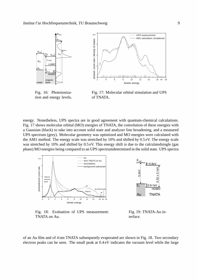
Fig. 17: Molecular orbital simulation and UPSof TNATA.
energy. Nonetheless, UPS spectra are in good agreement with quantum-chemical calculations.Fig. 17 shows molecular orbital (MO) energies of TNATA, the convolution of these energies witha Gaussian (black) to take into account solid state and analyzer line broadening, and a measuredUPS spectrum (grey). Molecular geometry was optimized and MO energies were calculated withthe AM1 method. The energy scale was stretched by 10% and shifted by 0.5 eV. The energy scalewas stretched by 10% and shifted by 0.5 eV. This energy shift is due to the calculatedsingle (gasphase) MO energies being compared to an UPS spectrumdetermined in the solid state. UPS spectra
-2 0 2 4 6 8 10 12 14 16 18
Au 4nm TNATA on Au secondaries background subtracted
TNATA
Au
Au Fermi level
TNATAvacuumlevel
IP
a.u.
eV
phot
oele
ctro
n co
unt
rate
kinetic energy
Fig. 18: Evaluation of UPS measurement:TNATA on Au.
Fig. 19: TNATA-Au in-terface.
of an Au film and of 4 nm TNATA subsequently evaporated are shown in Fig. 18. Two secondaryelectron peaks can be seen. The small peak at 0.4 eV indicates the vacuum level while the large

10 Annual report 1999/2000
peak is a result of electrons colliding with residual gas atoms during the flight towards the analyzer.The large secondary electron peak can satisfactorily be modeled by a Gaussian-broadened expo-nential function. Fig. 18 shows a corresponding fit (dashed) and the spectrum after subtraction.From Fig. 18, a contact barrier for hole injection of 0.9–1 eV can be derived. The vacuum leveldifference is on the order of 0.8 eV (Fig. 19).
0 2 4 6 8 10 12 14 16 18
NPD layer thickness
Au 4 nm CuPC / Au 0,3 nm NPD / 4 nm CuPc / Au 0,6 nm NPD / 4 nm CuPc / Au 1 nm NPD / 4 nm CuPc / Au 2 nm NPD / 4 nm CuPc / Au
Au
a.u.
eV
kinetic energy
phot
oele
ctro
n co
unt r
ate
Fig. 20: Interface formation: CuPc on Au andα-NPD on CuPc (successively).
Fig. 21: Au-CuPc-α-NPD interface.
Fig. 20 shows UPS spectra of Au, 4 nm CuPc evaporated on Au, and of α-NPD successivelyevaporated on top of the former layers. Measurements were taken at 0.3, 0.6, 1, and 2 nm α-NPDlayer thickness. The resulting energy level structure ist shown in Fig. 21. The hole injection barrierbetween Au and CuPc is approx. 0.73 eV, improving hole injection efficiency in comparison toTNATA. This result is confirmed by a significant improvement of OLED turn-on voltage if a 5 nmCuPc injection layer is introduced into the device. α-NPD on CuPc shows a slight energy levelupshift (“band bending”) at the interface. The HOMO energy level difference between α-NPD andCuPc is 0.4–0.5 eV for 1–2 nm α-NPD layer thickness, which is in good agreement with [15].
2.3 Dynamics
In the last years, the performance of organic light-emitting diodes (OLEDs) has been optimized,especially with regard to efficiency, stability and lifetime of the devices. Another criterion ofoptimization is the dynamic behaviour of luminescence which is important in view of optical com-munications and large flat-panel displays.
In molecular organic materials, light is generated by the decay of molecular excited states (exci-tons), that can be subdivided in spin-antisymmetric singlet and in spin-symmetric triplet excitons.While singlet excitons mainly decay radiatively and generate fluorescence, the energy of tripletexcitons mostly decay nonradiatively or lead to delayed luminescence known as phophorescence.

Institut f ur Hochfrequenztechnik, TU Braunschweig 11
The molecular excitation in electroluminescence results from the electrical pumping by injectionof charge carriers. On the other hand, the molecule can also be photoexcited by absorption of ahigh energy photon, followed by the creation of an exciton and its radiative relaxation known asphotoluminescence.
According to this, one can learn about the dynamics of the intrinsic excited state processes by us-ing time-resolved optical spectroscopy. With the help of a femtosecond laser system, it is possibleto measure the lifetimes τ of excited states. The thin films of the molecular material are excited byultrashort and very intensive UV-laser pulses ( � 100 fs), which may be produced by a mode-lockedtitanium:saphire solid state laser and a SHG (“Second Harmonic Generator”). A pulse picker maybe useful to reduce the repetition rate so that organic materials with longer luminescence decaytimes can also be examined.
Alq + h (390 nm)n3 Alq3
Alq + hn3
S *Ph-QdS
*
Ph-Qd + hn
Förster
energytransfer
a) b)wavelength
400 450 500 550 600 650 nm 700
a.u.
norm
alized inte
nsity
1.0
0.8
0.6
0.4
0.2
0.0
AlqPh-Qd:Alq3
3
Fig. 22: a) Photoluminescence spectra of Alq3 and Ph-Qd:Alq3, b) Relevant energy transfers ofthe guest-host system Ph-Qd:Alq3.
In the following, the dynamics of energy states are discussed with reference to the guest-hostsystem Ph-Qd:Alq3 [2]. The dopant Ph-Qd is coevaporated with the host material Alq3, so thatthe optical properties of the thin film change as illustrated in the photoluminescence spectra inFig. 22 a). The spectral halfwidth of the guest-host system Ph-Qd:Alq3 (FWHM=35 nm) is smallerthan that of the pure host material Alq3. Generally, the shape of the spectrum depends on thedoping concentration.
Fig. 22 b) illustrates the energy transfer processes relevant for the photoluminescence of the guest-host system Ph-Qd:Alq3. The pump energy is absorbed by an Alq3 host molecule. There are twoways of radiative relaxation for the excited state SAlq �3. Either the host molecule decays directlyto the ground state, which leads to the luminescence spectrum of pure Alq3, or the energy istransferred to the Ph-Qd acceptor molecule via the Forster energy transfer and Ph-Qd luminescenceoccurs. The Forster mechanism describes a nonradiative transfer of the singlet excited state froma host molecule to a dopant molecule by means of dipole–dipole coupling. The characteristic rateof this energy transfer can be termed by [16]
kF� τ � 1
d
�R0
r � 6
with R0�
�α � ∞
0
Ld�ν � εa
�ν �
ν4 dν � 1 � 6 �

12 Annual report 1999/2000
τd is the lifetime of the host molecule, r is the distance between donor and acceptor. R0 is the char-acteristic Forster distance, where Ld
�ν � and εa
�ν � are the luminescence and extinction spectra of
the donor and acceptor, respectively. It follows that a larger overlap between the two spectra leadsto a higher rate of Forster energy transfer. A typical distance for this energy transfer is approx.5 nm [16, 17]. α comprises the relative orientation of the dipole moment and material constants.
0,05 0,10 0,15 0,20 0,25 0,30 0,35 0,40 0,45
8
9
10
11
12
13
14
15
16ns
wt%
l = 528 nm
decay tim
e
dopant concentration
-500
0
500
1000
1500
2000
2500
3000
3500
4000
time0 10 20 30 40 ns 50
Ph-Qd: Alq 0,4 wt%3
a. u.
inte
nsity
Fig. 23: a) Time-resolved photoluminescence of a doped Ph-Qd:Alq3 layer, (b) decay times ofluminescence in dependence of the dopant concentration.
Conclusions can be drawn about the dynamics and lifetimes of excited states by using time-resolved optical spectroscopy. Fig. 23 a) shows a measurement result of the time-resolved pho-toluminescence spectrum of Ph-Qd:Alq3 with a dopant concentration of 0.4 wt%. This concentra-tion is a typical amount to obtain a high quantum yield and a reduction of exciton quenching byusing the advantage of efficient Forster energy transfer [18]. A time decay of about 9 ns can bedetermined. By examining thin films with different dopant concentrations, it can be found that thedecay time decreases with increasing dopant concentration (Fig. 23 b). This has been confirmedfor other guest-host materials, like DCM:Alq3 [19]. Therefore, it is possible to determine the con-centration of optically active dopant in an organic thin film by time-resolved optical spectroscopy.This will especially be useful for controlling the dopant concentration in emissive layers of organiclight emitting diodes.

Institut f ur Hochfrequenztechnik, TU Braunschweig 13
References
[1] C. W. Tang, S. A. VanSlyke, Appl. Phys. Lett. 51, 913 (1987).
[2] W. Kowalsky e.a., Adv. Solid State Phy. 39, 91 (1999).
[3] K. Nagayama, T. Yahagi, H. Nakada, T. Tohma, T. Watanabe, K. Yoshida, S. Miyaguchi,Jpn. J. Appl. Phys. 36, L1555 (1997).
[4] A. Tsumura, H. Koezuka, T. Ando, Appl. Phys. Lett. 49, 1210 (1986).
[5] Y.-Y. Lin, D. J. Gundlach, S. F. Nelson, T. N. Jackson, IEEE Electron Device Lett. 18, 606,(1997).
[6] G. Horowitz, X. Peng, D. Fichou, F. Garnier, J. Appl. Phys. 67, 528, (1990).
[7] J. G. Laquindanum, H. E. Katz, A. J. Lovinger, A. Dodabalapur, Chem. Mater. 8, 2542, (1996).
[8] E. Tutis, M.-N. Bussac, L. Zuppiroli, Appl. Phys. Let. 75, 3880. (1999).
[9] L. S. Hung, C. W. Tang, M. G. Mason, Appl. Phys. Let. 70, 152. (1996).
[10] G. E. Jabbour, Y. Kawabe, S. E. Shaheen e.a. Appl. Phys. Let. 71, 1762. (1997).
[11] R. Schlaf, B. A. Parkinson, Appl. Phys. Let. 84, 6729. (1998).
[12] S.Hufner, Photoelectron Spectroscopy. (Springer-Verlag Berlin, Heidelberg, New York1996).
[13] H. Ishii, K. Sugiyama, E. Ito, K. Seki, Adv. Mater. 1999 11, 605 (1999).
[14] D. Briggs, Handbook of X-Ray and Ultraviolet Photoelectron Spectroscopy. (Heyden Lon-don, Philadelphia, Rheine 1977, 1978).
[15] T.Chasse, C.-I. Wu, I.G. Hill, A. Kahn, J. Appl. Phys. 85, 6589 (1999).
[16] S. E. Shaheen, B. Kippelen, N. Peyghambarian e.a., J. Appl. Phys. 85, 7939 (1999).
[17] M. A. Baldo, D. F. O´Brian, M. E. Thompson, S. R. Forrest, Phys. Rev. B 60, 14422 (1999).
[18] H. Mattoussi, H. Murata, C. D. Merritt, Y. Iizumi, J. Kido, Z. H. Kafafi , J. Appl. Phys. 86,2642 (1999).
[19] V. G. Kozlov, V. Bulovic, P. E. Burrows, S. R. Forest e.a., J. Appl. Phys. 84, 4096 (1998).