Embed Size (px)
Citation preview
Full p
aper
© 2016 WILEY-VCH Verlag GmbH & Co. KGaA, Weinheim (1 of 8) 1600923wileyonlinelibrary.com
Overcoming Charge Collection Limitation at Solid/Liquid Interface by a Controllable Crystal Deficient Overlayer
Kan Zhang, Sandheep Ravishankar, Ming Ma, Ganapathy Veerappan, Juan Bisquert,* Francisco Fabregat-Santiago,* and Jong Hyeok Park*
DOI: 10.1002/aenm.201600923
visible-light harvesting in 2001.[3] Second, the “disorder-engineered” or hydro-genated TiO2 reported by Chen et al. provided a new concept for hydrogen generation that revealed an ingenious architecture composed of thin “crystal-deficient” TiO2 surrounding an ordered anatase crystal, which increased its photo-catalytic activity.[4] These studies triggered numerous follow-up studies and have been regarded as universal approaches that can be extended to other semi-conductor photocatalysts.[5–7] However, as mentioned by Dr. Diebold, the reason the “crystal-deficient” overlayer in TiO2 results in better photocatalytic ability is counterin-tuitive.[8] In general, photocatalysts should be highly crystalline to avoid the forma-tion of detrimental recombination sites, which is not the case for “crystal-deficient” TiO2 material. Therefore, numerous researchers have attempted to understand the chemical composition, electronic structure, and origin of the photocatalytic
activity in “crystal-deficient” TiO2.[9–19] These previous studies of “crystal-deficient” TiO2 using various reductive conditions have provided incomplete and even incompatible insights into the role of disordered TiO2. Another key fundamental question regarding water splitting at the solid/liquid interface (crystal-deficient TiO2/electrolyte) remains completely unaddressed in recent studies. Indeed, substantial performance gains from an overlayer in PEC reactions have been previously reported.[20–25] In particular, an amorphous or crystalline TiO2 overlayer may
Bulk and surface charge recombination of photoelectrode are two key processes that significantly hinder solar-to-fuel conversion of photoelec-trochemical cell (PEC). In this study, the function of a “crystal-deficient” overlayer is unveiled, which outperforms a traditionally used amorphous or crystalline overlayer in PEC water splitting by exhibiting a high conductivity and large electron diffusion length to enable unlimited electron collection. The optimized ≈2.5 nm thickness of the “crystal-deficient” shell results in a depletion layer with a width of 3 nm, which overcomes the flat band limita-tion of the photovoltage and increases the light absorptivity in the wavelength range from 300 to 420 nm. In addition, a 50-fold increase in the conductivity yields a one-order-of-magnitude increase in the diffusion length of an electron (Ln)(≈20 μm), allowing for unlimited electron collection in the 1.9 μm TiO2 nanowire array with the “crystal-deficient” shell. The controllable “crystal-deficient” overlayer in rutile TiO2 nanowires photoanode achieves a photocur-rent density greater than 2.0 mA cm−2 at 1.23 V versus reversible hydrogen electrode (RHE), a 1.18% applied bias photon-to-current efficiency at 0.49 V versus RHE, a faradaic efficiency greater than 93.5% at 0.6 V versus Pt under air mass 1.5G simulated solar light illumination (100 mW cm−2).
1. Introduction
Since the pioneering report by Fujishima and Honda on pho-toelectrochemical (PEC) water splitting using a TiO2 electrode in 1972,[1] the modification of TiO2 crystals to produce highly active photocatalysts has attracted much attention over the past several decades.[2] TiO2 crystals have experienced two significant modification revolutions. First, a yellow TiO2 produced by nitrogen-anion doping provided a new avenue to
Dr. K. Zhang, Prof. J. H. ParkDepartment of Chemical and Biomolecular EngineeringYonsei University50 Yonsei-ro, Seodaemun-gu, Seoul 120-749, Republic of KoreaE-mail: [email protected]. Ravishankar, Prof. J. Bisquert, Prof. F. Fabregat-SantiagoInstitute of Advanced Materials (INAM)Universitat Jaume I12006 Castelló, SpainE-mail: [email protected]; [email protected]. MaSKKU Advanced Institute of NanotechnologySungkyunkwan UniversitySuwon 440-746, Republic of Korea
Dr. G. VeerappanCentre for Solar Energy MaterialsInternational Advanced Research Centre for Powder Metallurgy and New Materials (ARCI)Hyderabad 500005, IndiaProf. J. BisquertDepartment of ChemistryFaculty of ScienceKing Abdulaziz UniversityJeddah 21589, Saudi Arabia
Adv. Energy Mater. 2017, 7, 1600923
www.advenergymat.dewww.advancedsciencenews.com
Full
paper
© 2016 WILEY-VCH Verlag GmbH & Co. KGaA, Weinheim1600923 (2 of 8) wileyonlinelibrary.com
passivate surface states at the solid/liquid interface to decrease electron–hole recombination pathways.[26–31] However, whether the thin “crystal-deficient” overlayer increases light absorption or promotes charge separation remains controversial.
In this study, we unveiled an in situ formed and controllable “crystal-deficient” overlayer where the nature of the improved photocatalytic performance of TiO2 nanowire (NW) arrays in a PEC water-splitting system was systematically investigated. The distinct PEC features resulted from the functions of the “crystal-deficient” overlayer, which is similar to conventional ones with respect to charge-carrier recombination losses but far exceeds the light-harvesting performance of conventional overlayers. These new insights guided our design and opti-mization of “crystal-deficient” overlayer in TiO2 NW arrays to achieve outstanding PEC water splitting. By employing a rutile-phase-selective “disorder-engineering” agent, the in situ formed “crystal-deficient” overlayer in rutile TiO2 (DeR-TiO2) NW arrays on an anatase TiO2 (A-TiO2) underlayer achieved a photocurrent density greater than 2.0 mA cm−2 at 1.23 V versus reversible hydrogen electrode (RHE)and a 1.18% applied bias photon-to-current efficiency (ABPE) at 0.49 V versus RHE under air mass (AM) 1.5G simulated solar light illumination (100 mW cm−2).
2. Results and Discussion
In our previous study, we reported an R-TiO2 selective “disorder-engineering” agent, which is a solvated electron liquid derived from a lithium-amine chelating agent (Li-ethanediamine, Li-EDA).[32] The solution-processable disorder engineering was carried out to hydrothermally grow an R-TiO2 NW array device, see scanning electron microscopy (SEM) micro-graph in Figure S1 (Supporting Information) by controlling reaction time (see the Supporting Information in detail). A
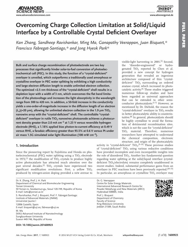
photograph of the DeR-TiO2 NW arrays on one device is shown in Figure 1a; the DeR-TiO2 NW arrays at the bottom are black, which distinguishes them from the ordered R-TiO2 NW arrays at the top. Accordingly, the valance-band (VB) X-ray photoelec-tron spectroscopy (XPS) results indicated a 1.47 eV upshift for the DeR-TiO2 NW arrays (Figure 1a). In comparison to ordered R-TiO2 arrays, the DeR-TiO2 NW arrays contained numerous oxygen vacancies that decrease in number from the outside to the inside, as revealed by O1s XPS, leading to the atomic arranging manners on the basal surface strongly disordered, as evidenced by high-resolution transmission electron micros-copy (HR-TEM) (Figure S2, Supporting Information). Electron energy loss spectroscopy (EELS) results suggest an inward reaction process that causes heterogeneous oxygen vacancies distribution (Figure S3, Supporting Information). The gra-dient defect is able to influence the local electronic structure when formed a heterojunction with order crystal. The HR-TEM images of these DeR-TiO2 NW arrays as a function of the treat-ment time are shown in Figure 1b–f, and the results indicate that the disordered overlayer was formed with a controllable thickness on the nanometer scale. Finally, a 14.8 nm disordered overlayer was formed on the crystalline R-TiO2 NW core after treatment for 2 min. The average diameter of the R-TiO2 NW arrays was determined to be ≈120 nm; the disordered shell/ordered core ratios are shown in Figure S4 (Supporting Infor-mation). The structural details of the core/shell relationship were further investigated by fast Fourier transform (FFT) of their HR-TEM images (inset in Figure 1b–f). After the first 5 s, the observed nanodomains corresponded to the (110), (111), and (001) atomic arrangements. The basal square shape was related to the tetragonal crystal of R-TiO2 (α = β = 90°, a = b ≠ c). However, these characterizations of tetragonal R-TiO2 changed as the treatment time increased. After 10 and 20 s, the basal square angle was distorted (α ≠ β ≠ 90°), and stretching of the lattice (a ≠ b) was observed at 1 and 2 min. These features may
Adv. Energy Mater. 2017, 7, 1600923
www.advenergymat.de www.advancedsciencenews.com
Figure 1. Characterization of “crystal-deficient” R-TiO2 NWs. a) VB-XPS spectra and a photograph of the ordered and “crystal-deficient” R-TiO2 NWs. b–f) HR-TEM images of the “crystal-deficient” R-TiO2 NWs as a function of treatment times: (b) 5 s, (c) 10 s, (d) 20 s, (e) 1 min, and (f) 2 min. The scale bar represents 2 nm. Insets in (b–f) are the FFT converted from the corresponding HR-TEM images.
Full p
aper
© 2016 WILEY-VCH Verlag GmbH & Co. KGaA, Weinheim (3 of 8) 1600923wileyonlinelibrary.com
be due to distortion of the periodic arrangement as the lattice vectors in the DeR-TiO2 NW arrays.[9] The distortion of electron conjugation along the ordered R-TiO2 NW core might lead to different interdomain electron transport. Their X-ray diffraction (XRD) patterns indicate a gradual weakening of rutile phase as the treatment time increased from 5 s to 2 min; this feature confirms “crystal-deficient” due to surface atomic arrangement disordering (Figure S5a, Supporting Information). Figure S5b shows the UV–vis diffuse reflectance spectra (DRS); the results indicate that the presence of “crystal-deficient” TiO2 substan-tially affected the light absorption of the R-TiO2 NW arrays. As the treatment time increased, a shift in the absorption edge toward higher wavelengths was observed. However, the extent of this shift was difficult to determine because the background absorption, which ranged from 400 to 800 nm, also increased. This result is consistent with the color changes.
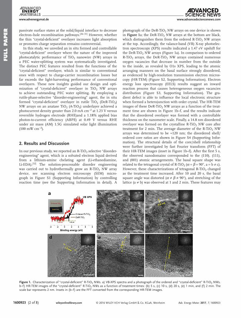
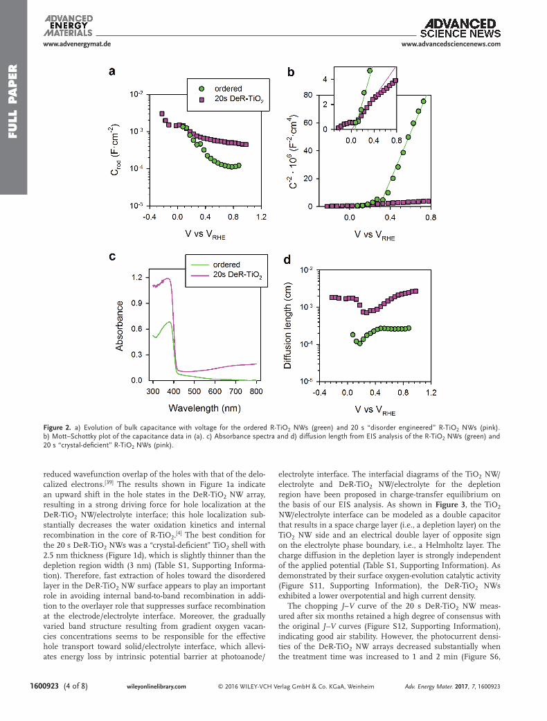
We evaluated the PEC water-splitting performance of the DeR-TiO2 NW arrays by measuring the photocurrent density–potential (J–V) curves using a standard three-electrode system with the arrays illuminated under AM 1.5G simulated solar light (Figure S6, Supporting Information). The photo-current density of the original ordered R-TiO2 NW arrays was 0.5 mA cm−2 at 1.23 VRHE. The photocurrent densities of the DeR-TiO2 NW arrays gradually increased with increasing treat-ment time, and the best value was 1.7 mA cm−2 at 1.23 VRHE after 20 s of disorder engineering. Notably, the photopotential was approximately the same (≈0.2 V vs RHE) for all of the samples, irrespective of the changes in the photocurrent; this similarity suggests that the same physicochemical process is limiting the increase in the open-circuit voltage (Voc). We carried out elec-trochemical impedance spectroscopy (EIS) measurements on a well-balanced DeR-TiO2 NW (20 s treatment) to elucidate the role of the disorder layer in PEC water splitting and com-pared the results to those obtained from ordered R-TiO2 NW arrays. The EIS results and corresponding equivalent circuits for ordered R-TiO2 and 20 s DeR-TiO2 are shown in Figure S7 (Supporting Information). The semi-arc obtained from ordered R-TiO2 was fitted to a transmission line (Figure S7a, Supporting Information), consistent with previous results reported for TiO2 and characteristic of electron diffusion in the conduction band (CB).[33,34] However, no characteristic features of electron transport were observed for the 20 s DeR-TiO2 NW, and the data were fitted to a simplified circuit (Figure S7b, Supporting Information), indicating a large improvement in electron con-ductivity. The evolution of the R-TiO2 NW capacitance was further investigated, as shown in Figure 2a. At high voltages, the 20 s DeR-TiO2 NW exhibited a capacitance one order of magnitude greater than that of the ordered R-TiO2 NW. How-ever, when the voltage approached Voc, the capacitances con-verged. The Mott–Schottky plots shown in Figure 2b indicate that the capacitance differences originated from the variation in the donor density (i.e., approximately two orders of magnitude) compared to the calculated values for the ordered R-TiO2 NW (3.2 × 1018 cm−3) and DeR-TiO2 NW (1.6 × 1020 cm−3). These donor density differences are very probably linked to a reduc-tion of Ti+4 atoms to Ti+3 induced by Li+ insertion reported for other TiO2 configurations.[35,36]
On the basis of the textural results and relative intrinsic electronic properties, the DeR-TiO2 NWs formed a well-defined
disorder layer, as confirmed by TEM observation, which affects the core of the R-TiO2 NWs. The results in Figure 2b indicate that the Voc values are slightly lower than the flat band poten-tial, which is nearly the same for both samples (80 ± 40 mV for ordered R-TiO2 and 7 ± 1 mV for DeR-TiO2 NWs), where the capacitances of the samples converge. The flat band poten-tial determines the upper limit for the increase in the electron Fermi level in TiO2 (and thus Voc). Notably, the Mott–Schottky plot of ordered TiO2 exhibits a flat region near the flat band. This region is associated with Fermi level pinning in a shallow energy level, which may be more easily discerned in the data collected under dark conditions, see Figure S8 (Supporting Information).[37]
The absorbance of the 20 s DeR-TiO2 NWs was greater than that of the ordered R-TiO2 in the complete spectrum (Figure 2c). However, absorption in the visible region of the spectrum did not produce and the response in the incident photon to current efficiency (IPCE) of the DeR-TiO2 NW array (Figure S9a, Supporting Information). The internal quantum efficiency also indicates that a strong enhancement only occurs in the wavelength region from 300 to 420 nm (Figure S9b, Sup-porting Information). Therefore we can conclude here that extension of TiO2 absorption to the visible region does not pro-duce an increase in the photocurrent density. The reason for this behavior is that states responsible for absorbing light in the visible region do not have sufficient energy to inject electrons into the CB of the ordered R-TiO2 core of the NWs. Then, potential contributors to the increased photocurrent density in DeR-TiO2 NWs are the increased absorption in the 300–420 nm region as shown in Figure 2c and enhanced charge collection efficiency of photogenerated charge. To evaluate charge collec-tion improvement, we used electron diffusion length (Ln) data plotted in Figure 2d. Ln was obtained from charge transfer and transport resistances obtained from impedance spectroscopy and calculations provided in the Supporting Information, see Figure S10 and Equation (S6) for more details. As shown in Figure 2d, Ln was ≈2 μm for the ordered R-TiO2 NW, which is only slightly larger than the wire thickness (1.9 μm). For the 20 s DeR-TiO2 NW, Ln raised one-order-of-magnitude to ≈20 μm, due to a 50-fold increase in electron conductivity that overcomes the increase in electron-loss observed in Figure S10 (Supporting Information). Estimations based on both the absorbance and Ln indicate that nearly all the photons absorbed in the 20 s DeR-TiO2 NWs were collected. However, for the ordered R-TiO2, the smaller Ln produces a loss of 21% of photogenerated electrons (see Table S2 in the Supporting Infor-mation). The rest should be attributed to differences in light absorbance stated above.
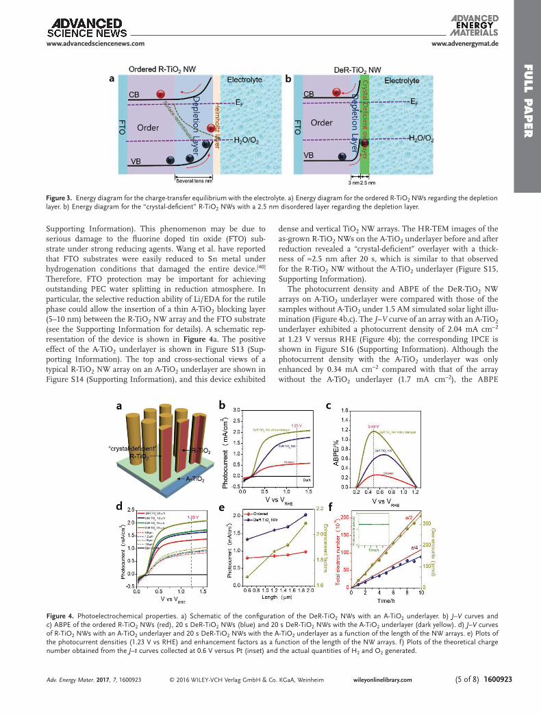
In general, in a PEC device whose photoanode or photo-cathode dimensions are larger than the typical depletion-layer thickness, the electric field is the primary force for charge sepa-ration. This electric field is induced at the electrode/electrolyte interface, where the equilibration of the Fermi level and the solution redox potential in the semiconductor and electrolyte, respectively, result in band bending and subsequent devel-opment of a depletion layer.[38] Consistent with theoretical simulations reported by Liu et al., for hydrogenated TiO2, the disordered TiO2 exhibited photogenerated holes with enhanced lifetimes because of trapping in the disordered part, which
Adv. Energy Mater. 2017, 7, 1600923
www.advenergymat.dewww.advancedsciencenews.com
Full
paper
© 2016 WILEY-VCH Verlag GmbH & Co. KGaA, Weinheim1600923 (4 of 8) wileyonlinelibrary.com
reduced wavefunction overlap of the holes with that of the delo-calized electrons.[39] The results shown in Figure 1a indicate an upward shift in the hole states in the DeR-TiO2 NW array, resulting in a strong driving force for hole localization at the DeR-TiO2 NW/electrolyte interface; this hole localization sub-stantially decreases the water oxidation kinetics and internal recombination in the core of R-TiO2.[4] The best condition for the 20 s DeR-TiO2 NWs was a “crystal-deficient” TiO2 shell with 2.5 nm thickness (Figure 1d), which is slightly thinner than the depletion region width (3 nm) (Table S1, Supporting Informa-tion). Therefore, fast extraction of holes toward the disordered layer in the DeR-TiO2 NW surface appears to play an important role in avoiding internal band-to-band recombination in addi-tion to the overlayer role that suppresses surface recombination at the electrode/electrolyte interface. Moreover, the gradually varied band structure resulting from gradient oxygen vacan-cies concentrations seems to be responsible for the effective hole transport toward solid/electrolyte interface, which allevi-ates energy loss by intrinsic potential barrier at photoanode/
electrolyte interface. The interfacial diagrams of the TiO2 NW/electrolyte and DeR-TiO2 NW/electrolyte for the depletion region have been proposed in charge-transfer equilibrium on the basis of our EIS analysis. As shown in Figure 3, the TiO2 NW/electrolyte interface can be modeled as a double capacitor that results in a space charge layer (i.e., a depletion layer) on the TiO2 NW side and an electrical double layer of opposite sign on the electrolyte phase boundary, i.e., a Helmholtz layer. The charge diffusion in the depletion layer is strongly independent of the applied potential (Table S1, Supporting Information). As demonstrated by their surface oxygen-evolution catalytic activity (Figure S11, Supporting Information), the DeR-TiO2 NWs exhibited a lower overpotential and high current density.
The chopping J–V curve of the 20 s DeR-TiO2 NW meas-ured after six months retained a high degree of consensus with the original J–V curves (Figure S12, Supporting Information), indicating good air stability. However, the photocurrent densi-ties of the DeR-TiO2 NW arrays decreased substantially when the treatment time was increased to 1 and 2 min (Figure S6,
Adv. Energy Mater. 2017, 7, 1600923
www.advenergymat.de www.advancedsciencenews.com
Figure 2. a) Evolution of bulk capacitance with voltage for the ordered R-TiO2 NWs (green) and 20 s “disorder engineered” R-TiO2 NWs (pink). b) Mott–Schottky plot of the capacitance data in (a). c) Absorbance spectra and d) diffusion length from EIS analysis of the R-TiO2 NWs (green) and 20 s “crystal-deficient” R-TiO2 NWs (pink).
Full p
aper
© 2016 WILEY-VCH Verlag GmbH & Co. KGaA, Weinheim (5 of 8) 1600923wileyonlinelibrary.com
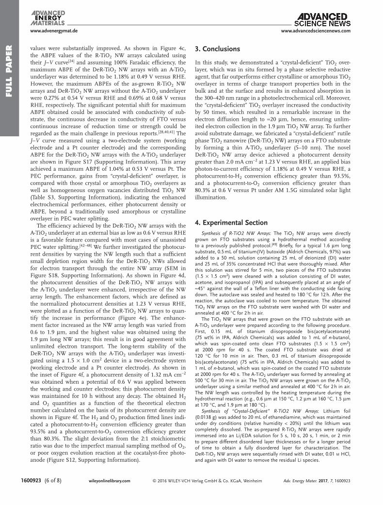
Supporting Information). This phenomenon may be due to serious damage to the fluorine doped tin oxide (FTO) sub-strate under strong reducing agents. Wang et al. have reported that FTO substrates were easily reduced to Sn metal under hydrogenation conditions that damaged the entire device.[40] Therefore, FTO protection may be important for achieving outstanding PEC water splitting in reduction atmosphere. In particular, the selective reduction ability of Li/EDA for the rutile phase could allow the insertion of a thin A-TiO2 blocking layer (5–10 nm) between the R-TiO2 NW array and the FTO substrate (see the Supporting Information for details). A schematic rep-resentation of the device is shown in Figure 4a. The positive effect of the A-TiO2 underlayer is shown in Figure S13 (Sup-porting Information). The top and cross-sectional views of a typical R-TiO2 NW array on an A-TiO2 underlayer are shown in Figure S14 (Supporting Information), and this device exhibited
dense and vertical TiO2 NW arrays. The HR-TEM images of the as-grown R-TiO2 NWs on the A-TiO2 underlayer before and after reduction revealed a “crystal-deficient” overlayer with a thick-ness of ≈2.5 nm after 20 s, which is similar to that observed for the R-TiO2 NW without the A-TiO2 underlayer (Figure S15, Supporting Information).
The photocurrent density and ABPE of the DeR-TiO2 NW arrays on A-TiO2 underlayer were compared with those of the samples without A-TiO2 under 1.5 AM simulated solar light illu-mination (Figure 4b,c). The J–V curve of an array with an A-TiO2 underlayer exhibited a photocurrent density of 2.04 mA cm−2 at 1.23 V versus RHE (Figure 4b); the corresponding IPCE is shown in Figure S16 (Supporting Information). Although the photocurrent density with the A-TiO2 underlayer was only enhanced by 0.34 mA cm−2 compared with that of the array without the A-TiO2 underlayer (1.7 mA cm−2), the ABPE
Adv. Energy Mater. 2017, 7, 1600923
www.advenergymat.dewww.advancedsciencenews.com
Figure 3. Energy diagram for the charge-transfer equilibrium with the electrolyte. a) Energy diagram for the ordered R-TiO2 NWs regarding the depletion layer. b) Energy diagram for the “crystal-deficient” R-TiO2 NWs with a 2.5 nm disordered layer regarding the depletion layer.
Figure 4. Photoelectrochemical properties. a) Schematic of the configuration of the DeR-TiO2 NWs with an A-TiO2 underlayer. b) J–V curves and c) ABPE of the ordered R-TiO2 NWs (red), 20 s DeR-TiO2 NWs (blue) and 20 s DeR-TiO2 NWs with the A-TiO2 underlayer (dark yellow). d) J–V curves of R-TiO2 NWs with an A-TiO2 underlayer and 20 s DeR-TiO2 NWs with the A-TiO2 underlayer as a function of the length of the NW arrays. e) Plots of the photocurrent densities (1.23 V vs RHE) and enhancement factors as a function of the length of the NW arrays. f) Plots of the theoretical charge number obtained from the J–t curves collected at 0.6 V versus Pt (inset) and the actual quantities of H2 and O2 generated.
Full
paper
© 2016 WILEY-VCH Verlag GmbH & Co. KGaA, Weinheim1600923 (6 of 8) wileyonlinelibrary.com
values were substantially improved. As shown in Figure 4c, the ABPE values of the R-TiO2 NW arrays calculated using their J–V curve[24] and assuming 100% Faradaic efficiency, the maximum ABPE of the DeR-TiO2 NW arrays with an A-TiO2 underlayer was determined to be 1.18% at 0.49 V versus RHE. However, the maximum ABPEs of the as-grown R-TiO2 NW arrays and DeR-TiO2 NW arrays without the A-TiO2 underlayer were 0.27% at 0.54 V versus RHE and 0.69% at 0.68 V versus RHE, respectively. The significant potential shift for maximum ABPE obtained could be associated with conductivity of sub-strate, the continuous decrease in conductivity of FTO versus continuous increase of reduction time or strength could be regarded as the main challenge in previous reports.[28,40,41] The J–V curve measured using a two-electrode system (working electrode and a Pt counter electrode) and the corresponding ABPE for the DeR-TiO2 NW arrays with the A-TiO2 underlayer are shown in Figure S17 (Supporting Information). This array achieved a maximum ABPE of 1.04% at 0.53 V versus Pt. The PEC performance, gains from “crystal-deficient” overlayer, is compared with those crystal or amorphous TiO2 overlayers as well as homogeneous oxygen vacancies distributed TiO2 NW (Table S3, Supporting Information), indicating the enhanced electrochemical performances, either photocurrent density or ABPE, beyond a traditionally used amorphous or crystalline overlayer in PEC water splitting.
The efficiency achieved by the DeR-TiO2 NW arrays with the A-TiO2 underlayer at an external bias as low as 0.6 V versus RHE is a favorable feature compared with most cases of unassisted PEC water splitting.[42–48] We further investigated the photocur-rent densities by varying the NW length such that a sufficient small depletion region width for the DeR-TiO2 NWs allowed for electron transport through the entire NW array (SEM in Figure S18, Supporting Information). As shown in Figure 4d, the photocurrent densities of the DeR-TiO2 NW arrays with the A-TiO2 underlayer were enhanced, irrespective of the NW array length. The enhancement factors, which are defined as the normalized photocurrent densities at 1.23 V versus RHE, were plotted as a function of the DeR-TiO2 NW arrays to quan-tify the increase in performance (Figure 4e). The enhance-ment factor increased as the NW array length was varied from 0.6 to 1.9 μm, and the highest value was obtained using the 1.9 μm long NW arrays; this result is in good agreement with unlimited electron transport. The long-term stability of the DeR-TiO2 NW arrays with the A-TiO2 underlayer was investi-gated using a 1.5 × 1.0 cm2 device in a two-electrode system (working electrode and a Pt counter electrode). As shown in the inset of Figure 4f, a photocurrent density of 1.32 mA cm−2 was obtained when a potential of 0.6 V was applied between the working and counter electrodes; this photocurrent density was maintained for 10 h without any decay. The obtained H2 and O2 quantities as a function of the theoretical electron number calculated on the basis of its photocurrent density are shown in Figure 4f. The H2 and O2 production fitted lines indi-cated a photocurrent-to-H2 conversion efficiency greater than 93.5% and a photocurrent-to-O2 conversion efficiency greater than 80.3%. The slight deviation from the 2:1 stoichiometric ratio was due to the imperfect manual sampling method of O2, or poor oxygen evolution reaction at the cocatalyst-free photo-anode (Figure S12, Supporting Information).
3. Conclusions
In this study, we demonstrated a “crystal-deficient” TiO2 over-layer, which was in situ formed by a phase selective reductive agent, that far outperforms either crystalline or amorphous TiO2 overlayer in terms of charge transport properties both in the bulk and at the surface and results in enhanced absorption in the 300–420 nm range in a photoelectrochemical cell. Moreover, the “crystal-deficient” TiO2 overlayer increased the conductivity by 50 times, which resulted in a remarkable increase in the electron diffusion length to ≈20 μm, hence, ensuring unlim-ited electron collection in the 1.9 μm TiO2 NW array. To further avoid substrate damage, we fabricated a “crystal-deficient” rutile phase TiO2 nanowire (DeR-TiO2 NW) arrays on a FTO substrate by forming a thin A-TiO2 underlayer (5–10 nm). The novel DeR-TiO2 NW array device achieved a photocurrent density greater than 2.0 mA cm−2 at 1.23 V versus RHE, an applied bias photon-to-current efficiency of 1.18% at 0.49 V versus RHE, a photocurrent-to-H2 conversion efficiency greater than 93.5%, and a photocurrent-to-O2 conversion efficiency greater than 80.3% at 0.6 V versus Pt under AM 1.5G simulated solar light illumination.
4. Experimental SectionSynthesis of R-TiO2 NW Arrays: The TiO2 NW arrays were directly
grown on FTO substrates using a hydrothermal method according to a previously published protocol.[49] Briefly, for a typical 1.6 μm long substrate, 0.5 mL of titanium(IV) butoxide (Aldrich Chemicals, 97%) was added to a 50 mL solution containing 25 mL of deionized (DI) water and 25 mL of 35% concentrated HCl that were thoroughly mixed. After this solution was stirred for 5 min, two pieces of the FTO substrates (1.5 × 1.5 cm2) were cleaned with a solution consisting of DI water, acetone, and isopropanol (IPA) and subsequently placed at an angle of ≈45° against the wall of a Teflon liner with the conducting side facing down. The autoclave was sealed and heated to 180 °C for 12 h. After the reaction, the autoclave was cooled to room temperature. The obtained TiO2 NW arrays on the FTO substrate were washed with DI water and annealed at 400 °C for 2 h in air.
The TiO2 NW arrays that were grown on the FTO substrate with an A-TiO2 underlayer were prepared according to the following procedure. First, 0.15 mL of titanium diisopropoxide bis(acetylacetonate) (75 wt% in IPA, Aldrich Chemicals) was added to 1 mL of n-butanol, which was spin-coated onto clean FTO substrates (1.5 × 1.5 cm2) at 2000 rpm for 40 s. The coated FTO substrate was dried at 120 °C for 10 min in air. Then, 0.3 mL of titanium diisopropoxide bis(acetylacetonate) (75 wt% in IPA, Aldrich Chemicals) was added to 1 mL of n-butanol, which was spin-coated on the coated FTO substrate at 2000 rpm for 40 s. The A-TiO2 underlayer was formed by annealing at 500 °C for 30 min in air. The TiO2 NW arrays were grown on the A-TiO2 underlayer using a similar method and annealed at 400 °C for 2 h in air. The NW length was controlled by the heating temperature during the hydrothermal reaction (e.g., 0.6 μm at 150 °C, 1.2 μm at 160 °C, 1.5 μm at 170 °C, and 1.9 μm at 180 °C).
Synthesis of “Crystal-Deficient” R-TiO2 NW Arrays: Lithium foil (0.0138 g) was added to 20 mL of ethanediamine, which was maintained under dry conditions (relative humidity < 20%) until the lithium was completely dissolved. The as-prepared R-TiO2 NW arrays were rapidly immersed into an Li/EDA solution for 5 s, 10 s, 20 s, 1 min, or 2 min to prepare different disordered layer thicknesses or for a longer period of time to obtain a fully disordered layer for characterization. The DeR-TiO2 NW arrays were sequentially rinsed with DI water, 0.01 m HCl, and again with DI water to remove the residual Li species.
Adv. Energy Mater. 2017, 7, 1600923
www.advenergymat.de www.advancedsciencenews.com
Full p
aper
© 2016 WILEY-VCH Verlag GmbH & Co. KGaA, Weinheim (7 of 8) 1600923wileyonlinelibrary.com
Material Characterization: SEM images of the products were recorded on a field-emission scanning electron microscope (JSM-7000F, Japan). The XRD patterns were obtained with a D500/5000 diffractometer operated in Bragg–Brentano geometry and equipped with a Cu-Kα radiation source. The HR-TEM observations were performed on a JEOL JEM-AFM 200F (Japan) electron microscope with (Cs-corrected/energy-dispersive X-ray spectroscopy (EDS)/EELS). The VB-XPS and XPS measurements were performed on an auger electron spectroscopy (AES) XPS instrument (ESCA2000 from VG Microtech in England) equipped with an aluminum anode (Al Kα, λ = 1486.6 eV). The UV–vis DRS spectra were recorded using a UV–vis spectrophotometer (Shimadzu UV-2550).
Electrochemical Analysis: Cyclic voltammetry and EIS scans were performed using a three-electrode configuration on a frequency response analyzer (FRA)-equipped potentiostat from Autolab and a Keithley 2612 system source meter. The counter electrode consisted of a coiled Pt wire, and the electrolyte was 1 m NaOH solution. The cyclic voltammetry measurements were performed at a scan rate of 50 mV s−1 in the dark and under illumination at 1 sun (100 mW cm−2) using a 150 W Xe lamp. The amplitude of the perturbation signal for the EIS measurements was 10 mV, and the scanning frequency range was 50 mHz–1000 kHz.
PEC Measurements: The PEC performance was measured using a potentiostat (CH Instruments, CHI 660) in a three-electrode optical “O-ring” cell (0.37 cm2) with a Pt foil counter electrode and a saturated Ag/AgCl reference electrode (in 3 m saturated KCl) under AM 1.5G simulated solar light illumination (100 mW cm−2) from a 150 W xenon lamp solar simulator (PEC-L01, PECCELL, Yokohama, Japan). Before the measurements, the solar simulator intensity was calibrated with a reference silicon solar cell (VLSI standards, Oriel P/N 91150 V). 30 mL of a 1 m NaOH solution (pH ≈ 14) containing 2 mL of methanol was used as the electrolyte. The conversion between the potentials versus Ag/AgCl and versus RHE was performed using the following equation
vsRHE vs Ag/AgCl reference 0.0591V pHAg/AgClE E E( ) ( ) ( )= + + × (1)
reference 0.1976V vsNHE at 25 CAg/AgClE( )( ) = °
(2)
Prior to the PEC measurements, the electrolyte was purged with N2 to remove dissolved oxygen. In a typical J–V measurement, linear sweep voltammetry was conducted at a scan rate of 20 mV s−1. The IPCE was measured at 0.5 V versus VRHE using a monochromator (Polaronix K3100 IPCE measurement system, McScience) with a 300 W xenon light source.
The ABPE was calculated from the J–V curve by assuming 100% Faradaic efficiency using the equation
ABPE%1.23 Vbias
in
J VP
( )( )=× −
(3)
where J was the photocurrent density (mA cm−2), Vbias was the applied bias between working electrode and RHE, and Pin was the incident illumination power density (AM 1.5G, 100 mW cm−2). The ABPE was also calculated using a J–V curve obtained from a two-electrode system where Vbias was the applied bias between the working electrode and Pt.
The PEC water splitting was carried out in a quartz reactor, which was sealed with rubber plugs and Parafilm. The electrode (1.5 × 1 cm2) and Pt foil (1.5 × 1 cm2) were immersed in the electrolyte in a two-electrode configuration with a 0.6 V absolute bias. Prior to the reaction and the sealing process, the electrolyte (1 m NaOH, adjusted to pH 7 with a phosphate buffer) was purged with N2 gas. Each hour, 1 mL of gas was analyzed by gas chromatography (Agilent Technologies 7890A GC system, USA) using a 5 Å molecular sieve column and Ar as the
carrier gas. The experimental error for the evolution of H2 and O2 was considered to be ≈3%.
The theoretical electron number as a function of the J–t curve was calculated on the basis of an area of 1.5 × 1 cm2
Theoretical electronnumber
current density 1.5 6.24146 10180
10
t h
t h∫= × × ×=
=
(4)
The photocurrent-to-H2 conversion efficiency and photocurrent-to-O2 conversion efficiency were determined on the basis of their linear slopes
(i.e., theoretical electronnumber2
for the photocurrent-to-H2 conversion
efficiency and theoretical electronnumber4
for the photocurrent-to-O2 conversion efficiency).
Supporting InformationSupporting Information is available from the Wiley Online Library or from the author.
AcknowledgementsK.Z. and S.R. contributed equally to this work. This work was supported by the NRF of Korea Grant funded by the Ministry of Science, ICT, and Future Planning (NRF-2013R1A2A1A09014038, 2015M1A2A2074663, 2016M3D3A1A01913254 (C1 Gas Refinery Program)). This work was supported in part by the Yonsei University Future-leading Research Initiative of 2015 (2015-22-0067). S.R. thanks the Santiago Grisolía program from Generalitat Valenciana for its financial support under the grant 2014/034. The work at INAM-UJI was supported by the Generalitat Valenciana project PROMETEOII/2014/020.
Received: May 3, 2016Revised: July 10, 2016
Published online: October 13, 2016
[1] A. Fujishima, K. Honda, Nature 1972, 238, 37.[2] X. B. Chen, S. S. Mao, Chem. Rev. 2007, 107, 2891.[3] R. Asahi, T. Morikawa, T. Ohwaki, K. Aoki, Y. Taga, Science 2001,
293, 269.[4] X. B. Chen, J. Liu, Y. Y. Peter, S. S. Mao, Science 2011, 331, 746.[5] H. Tong, S. X. Ouyang, Y. P. Bi, N. Umezawa, M. Oshikiri, J. H. Ye,
Adv. Mater. 2012, 24, 229.[6] G. M. Wang, Y. C. Ling, H. Y. Wang, X. Y. Yang, C. C. Wang,
J. Z. Zhang, Y. Li, Energy Environ. Sci. 2012, 5, 6180.[7] G. M. Wang, Y. C. Ling, X. H. Lu, F. Qian, Y. X. Tong, J. Z. Zhang,
V. Lordi, Y. Li, J. Phys. Chem. C 2013, 117, 10957.[8] U. Diebold, Nat. Chem. 2011, 3, 271.[9] M. K. Tian, M. Mahjouri-Samani, G. Eres, R. Sachan, M. Yoon,
M. F. Chisholm, K. Wang, A. A. Puretzky, C. M. Rouleau, D. B. Geohegan, G. Duscher, ACS Nano 2015, 9, 10482.
[10] M. I. Nandasiri, V. Shutthanandan, S. Manandhar, A. M. Schwarz, L. Oxenford, J. V. Kennedy, S. Thevuthasan, M. A. Henderson, J. Phys. Chem. Lett. 2015, 6, 4627.
[11] Y. Yang, Y. C. Ling, G. M. Wang, T. Y. Liu, F. X. Wang, T. Zhai, Y. X. Tong, Y. Li, Nano Lett. 2015, 15, 7051.
[12] X. B. Chen, J. Liu, F. Q. Huang, Chem. Soc. Rev. 2015, 44, 1861.
Adv. Energy Mater. 2017, 7, 1600923
www.advenergymat.dewww.advancedsciencenews.com
Full
paper
© 2016 WILEY-VCH Verlag GmbH & Co. KGaA, Weinheim1600923 (8 of 8) wileyonlinelibrary.com Adv. Energy Mater. 2017, 7, 1600923
www.advenergymat.de www.advancedsciencenews.com
[13] A. Danon, K. Bhattacharyya, B. K. Vijayan, J. L. Lu, D. J. Sauter, K. A. Gray, P. C. Stair, E. Weitz, ACS Catal. 2012, 2, 45.
[14] C. Sun, Y. Jia, X. H. Yang, H. G. Yang, X. D. Yao, G. Q. Lu, A. Selloni, S. C. Smith, J. Phys. Chem. C 2011, 115, 25590.
[15] N. Liu, C. Schneider, D. Freitag, M. Hartmann, U. Venkatesan, J. Muller, E. Spiecker, P. Schmuki, Nano Lett. 2014, 14, 3309.
[16] Z. Wang, C. Y. Yang, T. Q. Lin, H. Yin, P. Chen, D. Y. Wan, F. F. Xu, F. Q. Huang, J. H. Lin, X. M. Xie, M. H. Jiang, Adv. Funct. Mater. 2013, 23, 5444.
[17] X. D. Jiang, Y. P. Zhang, J. Jiang, Y. S. Rong, Y. C. Wang, Y. C. Wu, C. X. Pan, J. Phys. Chem. C 2012, 116, 22619.
[18] A. Naldoni, M. Allieta, S. Santangelo, M. Marelli, F. Fabbri, S. Cappelli, C. L. Bianchi, R. Psaro, V. Dal Santo, J. Am. Chem. Soc. 2012, 134, 7600.
[19] S. Hoang, S. P. Berglund, N. T. Hahn, A. J. Bard, C. B. Mullins. J. Am. Chem. Soc. 2012, 134, 3659.
[20] K. Appavoo, M. Z. Liu, C. T. Black, M. Y. Sfeir, Nano Lett. 2015, 15, 1076.
[21] W. G. Yang, Y. H. Yu, M. B. Starr, X. Yin, Z. D. Li, A. Kvit, S. F. Wang, P. Zhao, X. D. Wang, Nano Lett. 2015, 15, 7574.
[22] Y. J. Hwang, C. Hahn, B. Liu, P. D. Yang, ACS Nano 2012, 6, 5060.
[23] L. Ji, M. D. McDaniel, S. J. Wang, A. B. Posadas, X. H. Li, H. Y. Huang, J. C. Lee, A. A. Demkov, A. J. Bard, J. G. Ekerdt, E. T. Yu, Nat. Nanotechnol. 2015, 10, 84.
[24] T. W. Kim, K. S. Choi. Science 2014, 343, 990.[25] M. J. Kenney, M. Gong, Y. G. Li, J. Z. Wu, J. Feng, M. Lanza,
H. J. Dai, Science 2013, 342, 836.[26] S. Hu, M. R. Shaner, J. A. Beardslee, M. Lichterman,
B. S. Brunschwig, N. S. Lewis, Science 2014, 344, 1005.[27] J. Gu, Y. Yan, J. L. Young, K. X. Steirer, N. R. Neale, J. A. Turner,
Nat. Mater. 2016, 15, 456.[28] P. L. Yan, G. J. Liu, C. M. Ding, H. X. Han, J. Y. Shi, Y. Gan, C. Li,
ACS Appl. Mater. Interfaces 2015, 7, 3791.[29] D. Eisenberg, H. S. Ahn, A. J. Bard, J. Am. Chem. Soc. 2014,
136, 14011.[30] Z. M. Bai, X. Q. Yan, Y. Li, Z. Kang, S. Y. Cao, Y. Zhang, Adv. Energy
Mater. 2016, 6, 1501459.
[31] I. S. Cho, H. S. Han, M. Logar, J. S. Park, X. L. Zheng, Adv. Energy Mater. 2016, 6, 1501840.
[32] K. Zhang, L. Y. Wang, J. K. Kim, M. Ma, G. Veerappan, C. L. Lee, K. J. Kong, H. Y. Lee, J. H. Park, Energy Environ. Sci. 2016, 9, 499.
[33] F. Fabregat-Santiago, J. Bisquert, G. Garcia-Belmonte, G. Boschloo, A. Hagfeldt, Sol. Energy Mater. Sol. C 2005, 87, 117.
[34] Q. Wang, S. Ito, M. Grätzel, F. Fabregat-Santiago, I. Mora-Sero, J. Bisquert, T. Bessho, H. Imai, J. Phys. Chem. B 2006, 110, 25210.
[35] M. P. Cantao, J. I. Cisneros, R. M. Torresi, J. Phys. Chem. 1994, 98, 4865.
[36] F. Giordano, A. Abate, J. P. Correa Baena, M. Saliba, T. Matsui, S. H. Im, S. M. Zakeeruddin, M. K. Nazeeruddin, A. Hagfeldt, M. Graetzel, Nat. Commun. 2016, 7, 10379.
[37] B. Klahr, S. Gimenez, F. Fabregat-Santiago, J. Bisquert, T. W. Hamann, J. Am. Chem. Soc. 2012, 134, 16693.
[38] R. Van de Krol, M. Grätzel, Electronic Materials: Science & Technology, Springer, New York, 2012.
[39] L. Liu, Y. Y. Peter, X. B. Chen, S. S. Mao, D. Z. Shen, Phys. Rev. Lett. 2013, 111, 065505.
[40] G. M. Wang, H. Y. Wang, Y. C. Ling, Y. C. Tang, X. Y. Yang, R. C. Fitzmorris, C. C. Wang, J. Z. Zhang, Y. Li, Nano Lett. 2011, 11, 3026.
[41] I. S. Cho, M. Logar, C. H. Lee, L. L. Cai, F. B. Prinz, X. L. Zheng, Nano Lett. 2014, 14, 24.
[42] M. G. Walter, E. L. Warren, J. R. McKone, S. W. Boettcher, Q. X. Mi, E. A. Santori, N. S. Lewis, Chem. Rev. 2010, 110, 6446.
[43] K. H. Shin, J. H. Park, ACS Appl. Mater. Interfaces 2015, 7, 18429.[44] F. F. Abdi, L. H. Han, A. H. M. Smets, M. Zeman, B. Dam,
R. van de Krol, Nat. Commun. 2013, 4, 2195.[45] J. W. Jang, C. Du, Y. Ye, Y. Lin, X. Yao, J. Thorne, E. Liu, G. McMahon,
J. F. Zhu, A. Javey, J. H. Guo, D. W. Wang, Nat. Commun. 2015, 6, 7447.
[46] X. J. Shi, K. Zhang, K. H. Shin, M. Ma, J. Kwon, I. T. Choi, J. K. Kim, H. K. Kim, D. H. Wang, J. H. Park, Nano Energy 2015, 13, 182.
[47] Y. S. Chen, J. S. Manser, P. V. Kamat, J. Am. Chem. Soc. 2015, 137, 974.[48] Gurudayal, D. Sabba, M. H. Kumar, L. H. Wong, J. Barber,
M. Grätzel, N. Mathews, Nano Lett. 2015, 15, 3833.[49] B. Liu, E. S. Aydil. J. Am. Chem. Soc. 2009, 131, 3985.