Embed Size (px)
Citation preview

Company Public – NXP, the NXP logo, and NXP secure connections for a smarter world are trademarks of NXP
B.V. All other product or service names are the property of their respective owners. © 2018 NXP B.V.
Mazyar Razzaz, Applications Engineering
Jeff Steinheider, Product Marketing
Overcoming DDR Challenges in High-Performance Designs
September 2018 | AMF-NET-T3267
COMPANY PUBLIC 1COMPANY PUBLIC 1
• Basic DDR SDRAM Structure
• DDR3 vs. DDR4 SDRAM Differences
• DDR Bring up Issues
• Configurations and Validation via QCVS
Tool
Agenda

COMPANY PUBLIC 2
BASIC DDR SDRAM
STRUCTURE
COMPANY PUBLIC 3
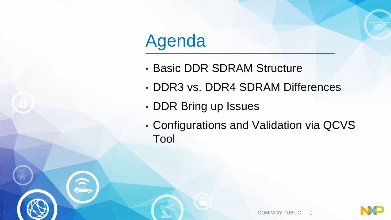
Single Transistor Memory Cell
S D
G
Cbit Ccol
Row (word) line
Column (bit) line
“1” => Vcc
“0” => Gnd
Vcc/2
“precharged” to Vcc/2
Storage
CapacitorParasitic Line
Capacitance
Access
Transistor
COMPANY PUBLIC 4
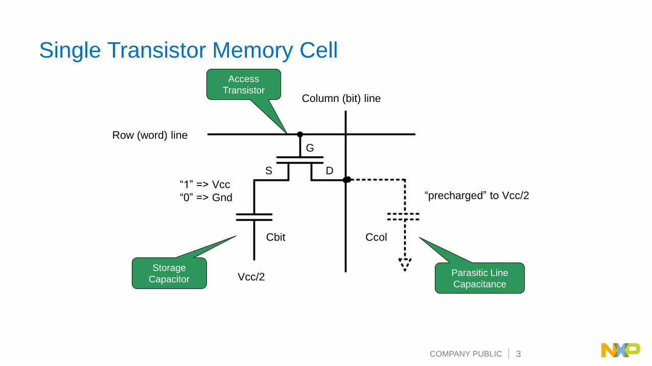
Memory Arrays
RO
W A
DD
RE
SS
DE
CO
DE
R
SENSE AMPS & WRITE DRIVERS
COLUMN ADDRESS DECODER
W0
B0
W1
W2
B1 B2 B3 B4 B5 B6 B7

COMPANY PUBLIC 5
Internal Memory Banks
• Multiple arrays organized into banks
• Multiple banks per memory device− DDR3 – 8 banks, and 3 bank address (BA) bits
− DDR4 – 16 banks with 4 banks in each of 4 sub bank groups
− Can have one active row in each bank at any given time
• Concurrency− Can be opening or closing a row in one bank while accessing
another bank
Bank 0
Row 0
Row 1
Row 3
Row 2
Bank 1 Bank 2 Bank 3
Row
Buffers
Row …
COMPANY PUBLIC 6
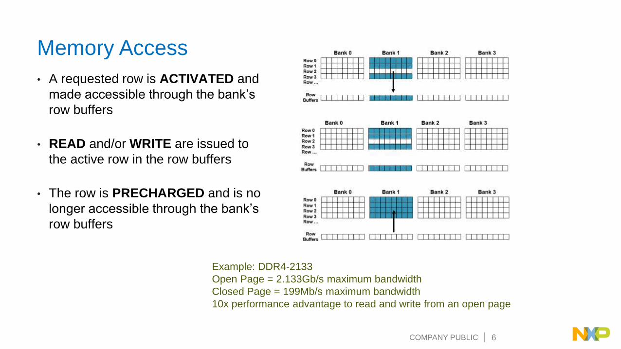
Memory Access
• A requested row is ACTIVATED and
made accessible through the bank’s
row buffers
• READ and/or WRITE are issued to
the active row in the row buffers
• The row is PRECHARGED and is no
longer accessible through the bank’s
row buffers
Example: DDR4-2133
Open Page = 2.133Gb/s maximum bandwidth
Closed Page = 199Mb/s maximum bandwidth
10x performance advantage to read and write from an open page
COMPANY PUBLIC 7
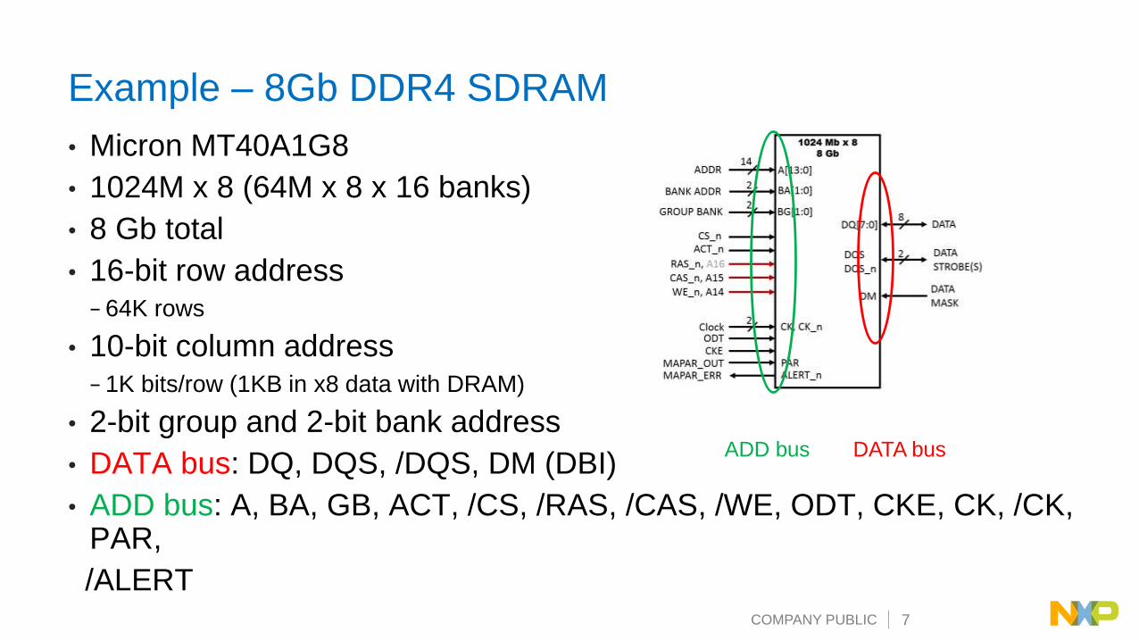
Example – 8Gb DDR4 SDRAM
• Micron MT40A1G8
• 1024M x 8 (64M x 8 x 16 banks)
• 8 Gb total
• 16-bit row address− 64K rows
• 10-bit column address− 1K bits/row (1KB in x8 data with DRAM)
• 2-bit group and 2-bit bank address
• DATA bus: DQ, DQS, /DQS, DM (DBI)
• ADD bus: A, BA, GB, ACT, /CS, /RAS, /CAS, /WE, ODT, CKE, CK, /CK, PAR,
/ALERT
DATA busADD bus
COMPANY PUBLIC 8
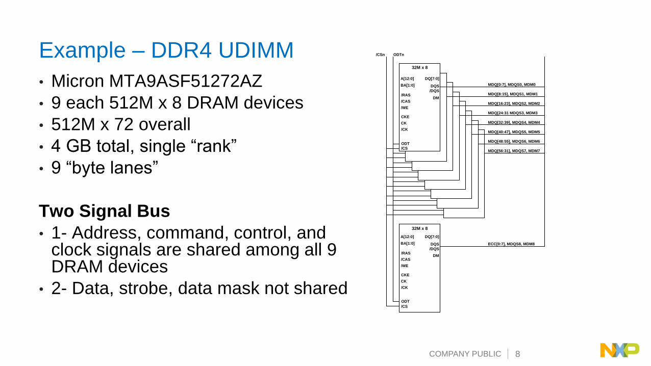
Example – DDR4 UDIMM
• Micron MTA9ASF51272AZ
• 9 each 512M x 8 DRAM devices
• 512M x 72 overall
• 4 GB total, single “rank”
• 9 “byte lanes”
Two Signal Bus
• 1- Address, command, control, and clock signals are shared among all 9 DRAM devices
• 2- Data, strobe, data mask not shared
32M x 8
/CS
/RAS
/CAS
/WE
CKE
CK
/CK
A[12:0]
BA[1:0]
DQ[7:0]
DQS
/DQS
DM
ODT
32M x 8
/CS
/RAS
/CAS
/WE
CKE
CK
/CK
A[12:0]
BA[1:0]
DQ[7:0]
DQS
/DQS
ODT
MDQ[0:7], MDQS0, MDM0
MDQ[48:55], MDQS6, MDM6
MDQ[8:15], MDQS1, MDM1
MDQ[16:23], MDQS2, MDM2
MDQ[24:31 MDQS3, MDM3
MDQ[32:39], MDQS4, MDM4
MDQ[40:47], MDQS5, MDM5
MDQ[56:31], MDQS7, MDM7
ECC[0:7], MDQS8, MDM8
/CSn ODTn
DM
COMPANY PUBLIC 9
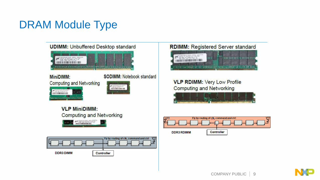
DRAM Module Type
COMPANY PUBLIC 10
DDR3 VS. DDR4 SDRAM
DIFFERENCES
COMPANY PUBLIC 11
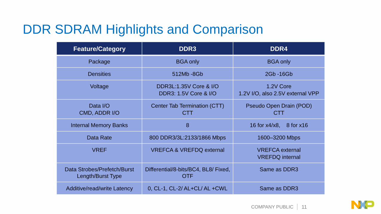
DDR SDRAM Highlights and Comparison
Feature/Category DDR3 DDR4
Package BGA only BGA only
Densities 512Mb -8Gb 2Gb -16Gb
Voltage DDR3L:1.35V Core & I/O
DDR3: 1.5V Core & I/O
1.2V Core
1.2V I/O, also 2.5V external VPP
Data I/O
CMD, ADDR I/O
Center Tab Termination (CTT)
CTT
Pseudo Open Drain (POD)
CTT
Internal Memory Banks 8 16 for x4/x8, 8 for x16
Data Rate 800 DDR3/3L:2133/1866 Mbps 1600–3200 Mbps
VREF VREFCA & VREFDQ external VREFCA external
VREFDQ internal
Data Strobes/Prefetch/Burst
Length/Burst Type
Differential/8-bits/BC4, BL8/ Fixed,
OTF
Same as DDR3
Additive/read/write Latency 0, CL-1, CL-2/ AL+CL/ AL +CWL Same as DDR3
COMPANY PUBLIC 12
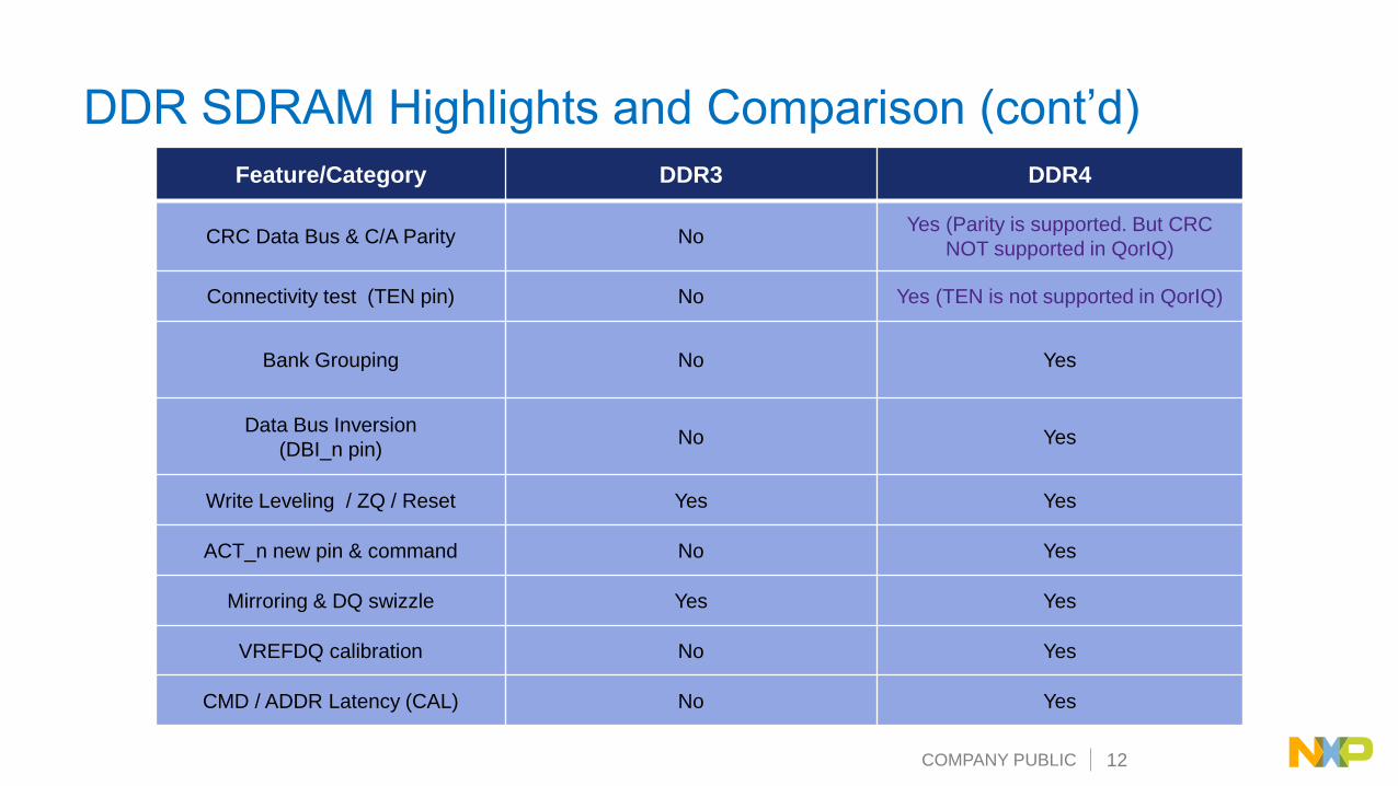
DDR SDRAM Highlights and Comparison (cont’d)
Feature/Category DDR3 DDR4
CRC Data Bus & C/A Parity NoYes (Parity is supported. But CRC
NOT supported in QorIQ)
Connectivity test (TEN pin) No Yes (TEN is not supported in QorIQ)
Bank Grouping No Yes
Data Bus Inversion
(DBI_n pin)No Yes
Write Leveling / ZQ / Reset Yes Yes
ACT_n new pin & command No Yes
Mirroring & DQ swizzle Yes Yes
VREFDQ calibration No Yes
CMD / ADDR Latency (CAL) No Yes
COMPANY PUBLIC 13
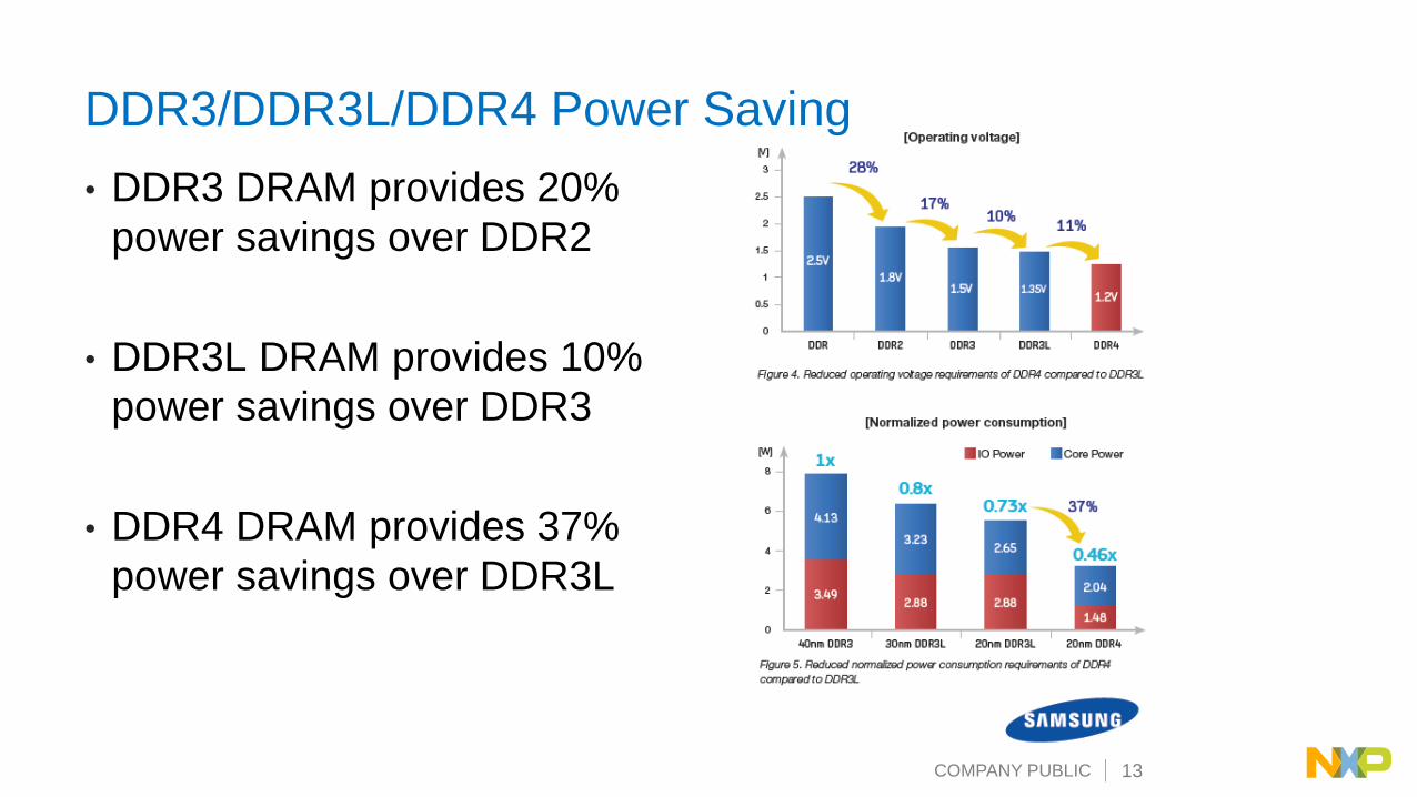
• DDR3 DRAM provides 20%
power savings over DDR2
• DDR3L DRAM provides 10%
power savings over DDR3
• DDR4 DRAM provides 37%
power savings over DDR3L
DDR3/DDR3L/DDR4 Power Saving
COMPANY PUBLIC 14
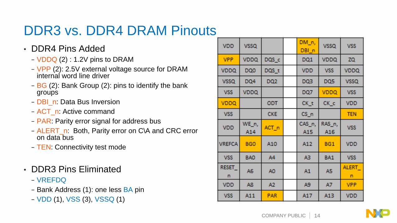
DDR3 vs. DDR4 DRAM Pinouts
• DDR4 Pins Added− VDDQ (2) : 1.2V pins to DRAM
− VPP (2): 2.5V external voltage source for DRAM internal word line driver
− BG (2): Bank Group (2): pins to identify the bank groups
− DBI_n: Data Bus Inversion
− ACT_n: Active command
− PAR: Parity error signal for address bus
− ALERT_n: Both, Parity error on C\A and CRC error on data bus
− TEN: Connectivity test mode
• DDR3 Pins Eliminated− VREFDQ
− Bank Address (1): one less BA pin
− VDD (1), VSS (3), VSSQ (1)
COMPANY PUBLIC 15
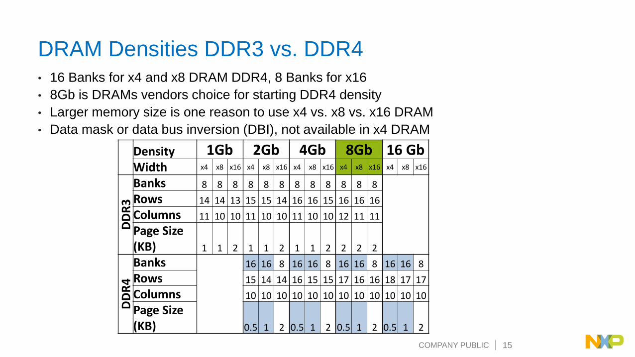
DRAM Densities DDR3 vs. DDR4• 16 Banks for x4 and x8 DRAM DDR4, 8 Banks for x16
• 8Gb is DRAMs vendors choice for starting DDR4 density
• Larger memory size is one reason to use x4 vs. x8 vs. x16 DRAM
• Data mask or data bus inversion (DBI), not available in x4 DRAM
Density 1Gb 2Gb 4Gb 8Gb 16 GbWidth x4 x8 x16 x4 x8 x16 x4 x8 x16 x4 x8 x16 x4 x8 x16
DD
R3
Banks 8 8 8 8 8 8 8 8 8 8 8 8
Rows 14 14 13 15 15 14 16 16 15 16 16 16
Columns 11 10 10 11 10 10 11 10 10 12 11 11
Page Size (KB) 1 1 2 1 1 2 1 1 2 2 2 2
DD
R4
Banks 16 16 8 16 16 8 16 16 8 16 16 8
Rows 15 14 14 16 15 15 17 16 16 18 17 17
Columns 10 10 10 10 10 10 10 10 10 10 10 10
Page Size (KB) 0.5 1 2 0.5 1 2 0.5 1 2 0.5 1 2
COMPANY PUBLIC 16
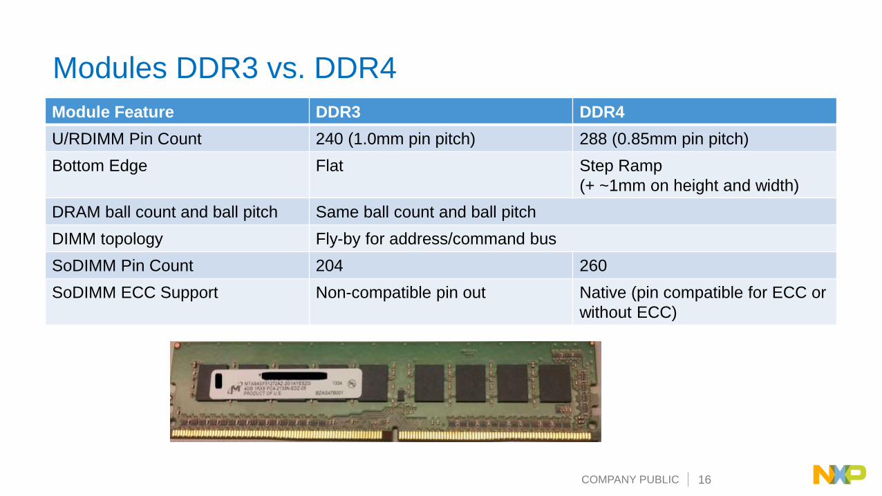
Modules DDR3 vs. DDR4
Module Feature DDR3 DDR4
U/RDIMM Pin Count 240 (1.0mm pin pitch) 288 (0.85mm pin pitch)
Bottom Edge Flat Step Ramp
(+ ~1mm on height and width)
DRAM ball count and ball pitch Same ball count and ball pitch
DIMM topology Fly-by for address/command bus
SoDIMM Pin Count 204 260
SoDIMM ECC Support Non-compatible pin out Native (pin compatible for ECC or
without ECC)
COMPANY PUBLIC 17
Why DDR4 Over DDR3
• Save power− DDR4 can reduce power by up to 40%
• Run faster− DDR4 offers double the data rate
− DDR4 doubles the number of internal banks, increased bandwidth
− New options to increase performance
• Better reliability & manufacturing capabilities− Connectivity test
− Data bus inversion (DBI)
− Internal VREF calibration
• Larger densities
• Longevity

COMPANY PUBLIC 18
DDR BRING UP ISSUES
COMPANY PUBLIC 19
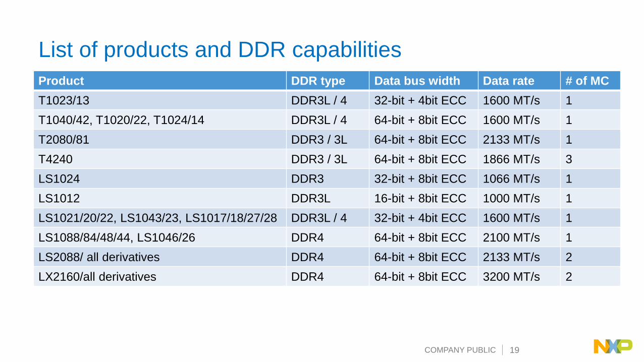
List of products and DDR capabilities
Product DDR type Data bus width Data rate # of MC
T1023/13 DDR3L / 4 32-bit + 4bit ECC 1600 MT/s 1
T1040/42, T1020/22, T1024/14 DDR3L / 4 64-bit + 8bit ECC 1600 MT/s 1
T2080/81 DDR3 / 3L 64-bit + 8bit ECC 2133 MT/s 1
T4240 DDR3 / 3L 64-bit + 8bit ECC 1866 MT/s 3
LS1024 DDR3 32-bit + 8bit ECC 1066 MT/s 1
LS1012 DDR3L 16-bit + 8bit ECC 1000 MT/s 1
LS1021/20/22, LS1043/23, LS1017/18/27/28 DDR3L / 4 32-bit + 4bit ECC 1600 MT/s 1
LS1088/84/48/44, LS1046/26 DDR4 64-bit + 8bit ECC 2100 MT/s 1
LS2088/ all derivatives DDR4 64-bit + 8bit ECC 2133 MT/s 2
LX2160/all derivatives DDR4 64-bit + 8bit ECC 3200 MT/s 2

COMPANY PUBLIC 20
List of DDR Bring up issues:
SW
Incorrect DQn_MAP setting
Setting WRLVL_START registers were incorrect
QCVS was not used, incorrect setting used
Erratum was not implemented
Incorrect data rate, not matching the generated setting
HW
Bring up, DRAM reset not matched to HRESET
Bring up, MDM pin, incorrect connection
Bring up, A/C layout causing ECC errors
Bring up, ACTn signal not connected
Bring up, DQS and DQS_B swapped
Bring up, incorrect bit swapping in layout
Bring up, Manufacturing issue on 2 out of 20 boards.
63%
37%
DDR BRING-UP ISSUES
SW + Reset HW
Top HW and SW DDR Issues
COMPANY PUBLIC 21
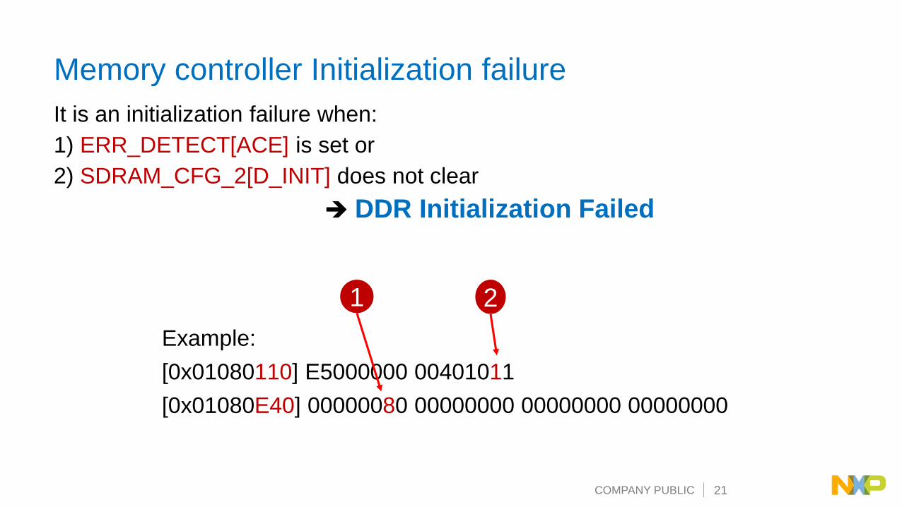
Memory controller Initialization failure
It is an initialization failure when:
1) ERR_DETECT[ACE] is set or
2) SDRAM_CFG_2[D_INIT] does not clear
DDR Initialization Failed
Example:
[0x01080110] E5000000 00401011
[0x01080E40] 00000080 00000000 00000000 00000000
1 2
COMPANY PUBLIC 22
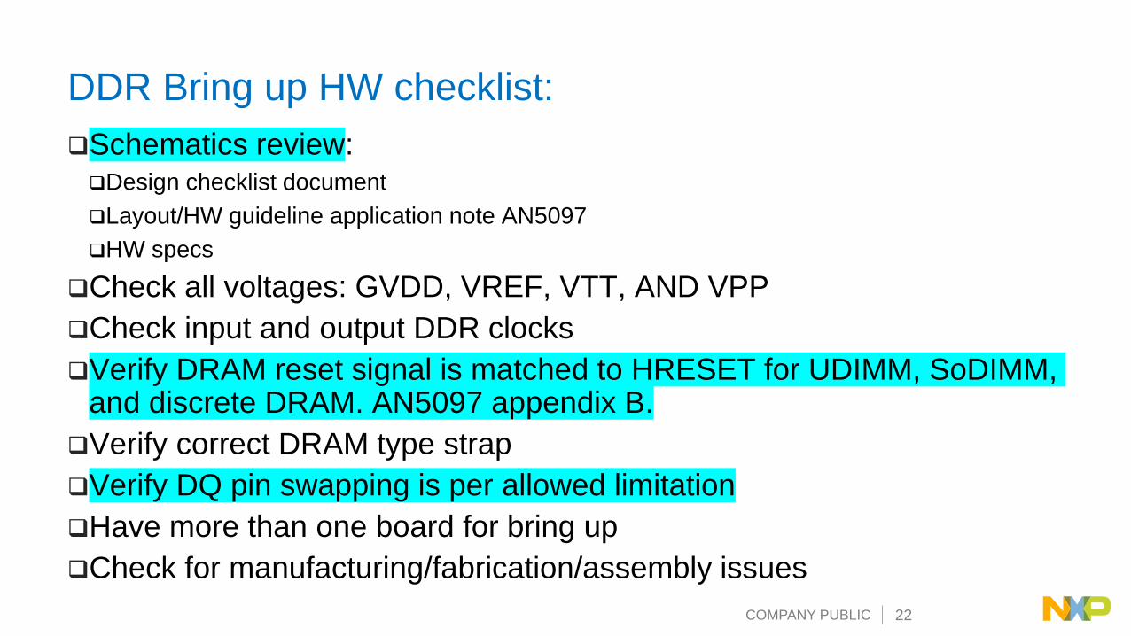
DDR Bring up HW checklist:
Schematics review:Design checklist document
Layout/HW guideline application note AN5097
HW specs
Check all voltages: GVDD, VREF, VTT, AND VPP
Check input and output DDR clocks
Verify DRAM reset signal is matched to HRESET for UDIMM, SoDIMM, and discrete DRAM. AN5097 appendix B.
Verify correct DRAM type strap
Verify DQ pin swapping is per allowed limitation
Have more than one board for bring up
Check for manufacturing/fabrication/assembly issues
COMPANY PUBLIC 23
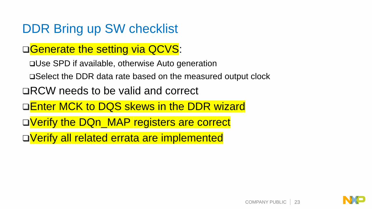
DDR Bring up SW checklist
Generate the setting via QCVS:
Use SPD if available, otherwise Auto generation
Select the DDR data rate based on the measured output clock
RCW needs to be valid and correct
Enter MCK to DQS skews in the DDR wizard
Verify the DQn_MAP registers are correct
Verify all related errata are implemented
COMPANY PUBLIC 24
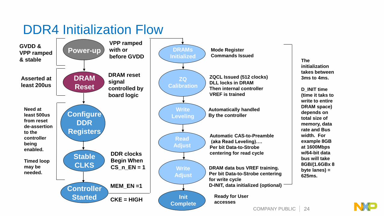
DDR4 Initialization Flow
Power-up
DRAM
Reset
Configure
DDR
Registers
DDR clocks
Begin When
CS_n_EN = 1
Asserted at
least 200us
Stable
CLKS
CKE = HIGH
DRAMs
Initialized
Mode Register
Commands Issued
ZQ
Calibration
Write
Leveling
Read
Adjust
Controller
Started
MEM_EN =1
Automatic CAS-to-Preamble
(aka Read Leveling)….
Per bit Data-to-Strobe
centering for read cycle
ZQCL Issued (512 clocks)
DLL locks in DRAM
Then internal controller
VREF is trained
Init
Complete
Ready for User
accesses
Automatically handled
By the controller
Need at
least 500us
from reset
de-assertion
to the
controller
being
enabled.
Timed loop
may be
needed. Write
Adjust
DRAM data bus VREF training.
Per bit Data-to-Strobe centering
for write cycle
D-INIT, data initialized (optional)
GVDD &
VPP ramped
& stable
VPP ramped
with or
before GVDD
DRAM reset
signal
controlled by
board logic
The
initialization
takes between
3ms to 4ms.
D_INIT time
(time it taks to
write to entire
DRAM space)
depends on
total size of
memory, data
rate and Bus
width. For
example 8GB
at 1600Mbps
w/64-bit data
bus will take
8GB/(1.6GBx 8
byte lanes) =
625ms.
COMPANY PUBLIC 25
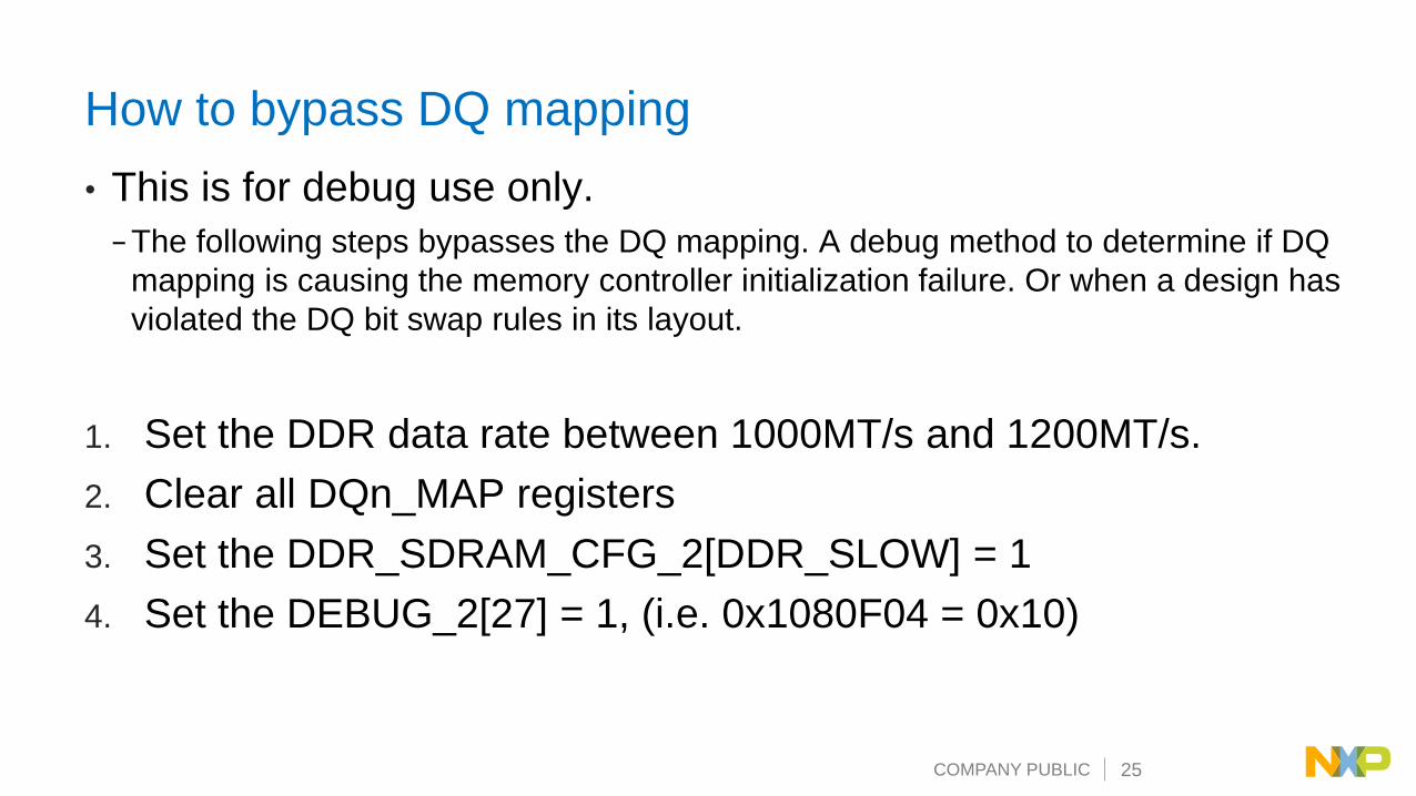
How to bypass DQ mapping
• This is for debug use only.
− The following steps bypasses the DQ mapping. A debug method to determine if DQ
mapping is causing the memory controller initialization failure. Or when a design has
violated the DQ bit swap rules in its layout.
1. Set the DDR data rate between 1000MT/s and 1200MT/s.
2. Clear all DQn_MAP registers
3. Set the DDR_SDRAM_CFG_2[DDR_SLOW] = 1
4. Set the DEBUG_2[27] = 1, (i.e. 0x1080F04 = 0x10)
COMPANY PUBLIC 26
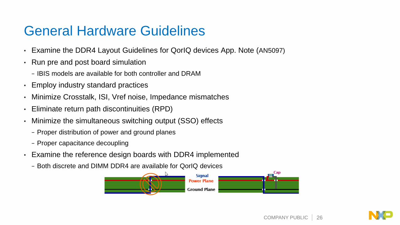
General Hardware Guidelines
• Examine the DDR4 Layout Guidelines for QorIQ devices App. Note (AN5097)
• Run pre and post board simulation
− IBIS models are available for both controller and DRAM
• Employ industry standard practices
• Minimize Crosstalk, ISI, Vref noise, Impedance mismatches
• Eliminate return path discontinuities (RPD)
• Minimize the simultaneous switching output (SSO) effects
− Proper distribution of power and ground planes
− Proper capacitance decoupling
• Examine the reference design boards with DDR4 implemented
− Both discrete and DIMM DDR4 are available for QorIQ devices
COMPANY PUBLIC 27
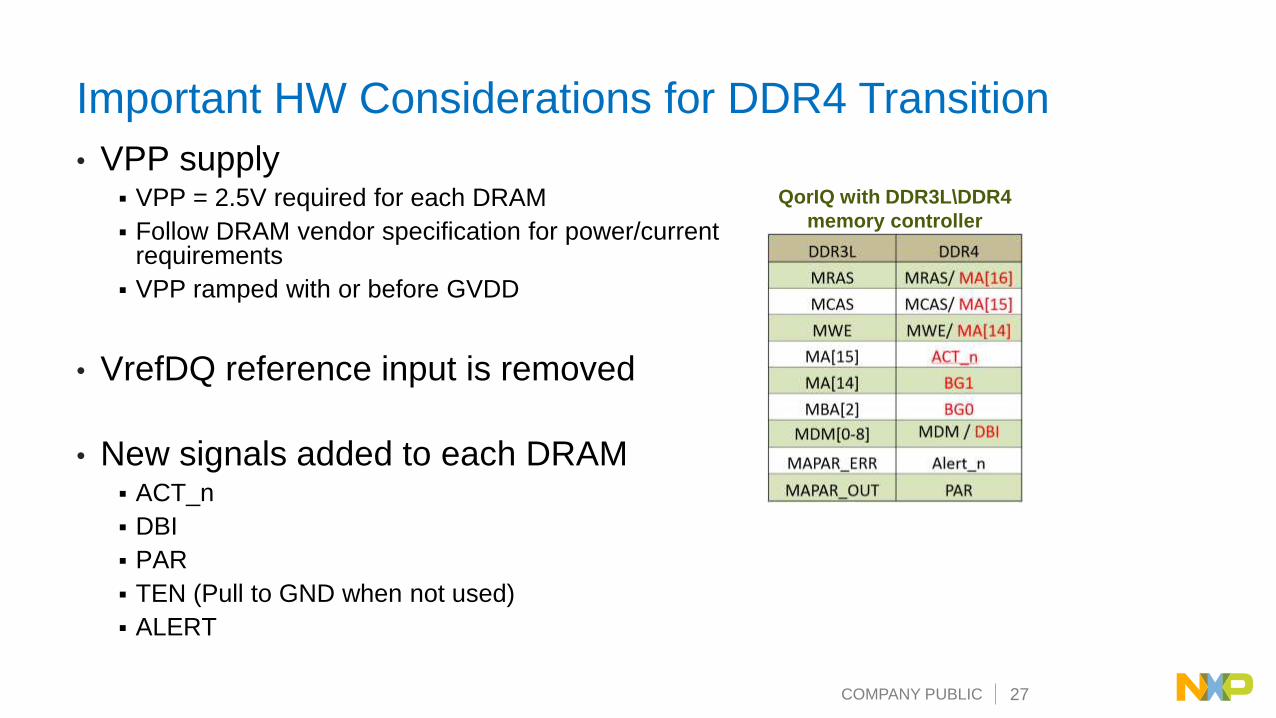
Important HW Considerations for DDR4 Transition
• VPP supply▪ VPP = 2.5V required for each DRAM
▪ Follow DRAM vendor specification for power/current requirements
▪ VPP ramped with or before GVDD
• VrefDQ reference input is removed
• New signals added to each DRAM▪ ACT_n
▪ DBI
▪ PAR
▪ TEN (Pull to GND when not used)
▪ ALERT
QorIQ with DDR3L\DDR4
memory controller
COMPANY PUBLIC 28
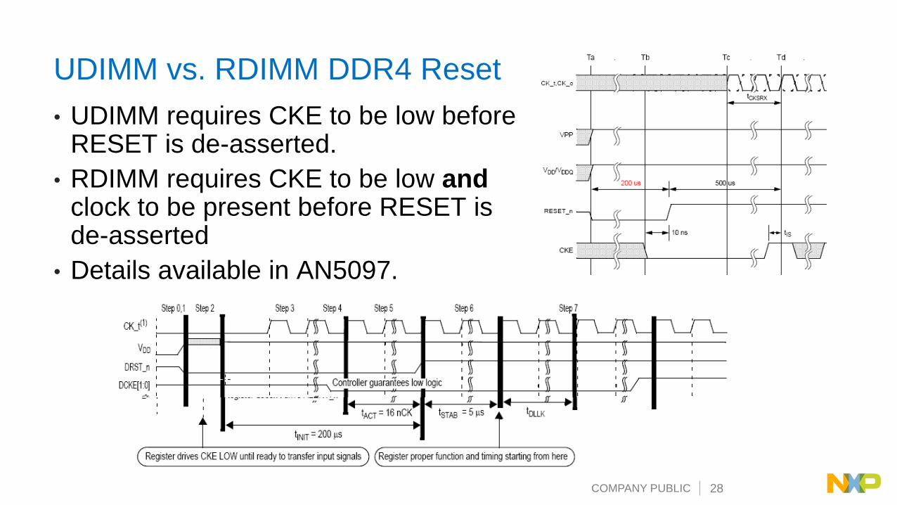
UDIMM vs. RDIMM DDR4 Reset
• UDIMM requires CKE to be low before RESET is de-asserted.
• RDIMM requires CKE to be low andclock to be present before RESET is de-asserted
• Details available in AN5097.
COMPANY PUBLIC 29
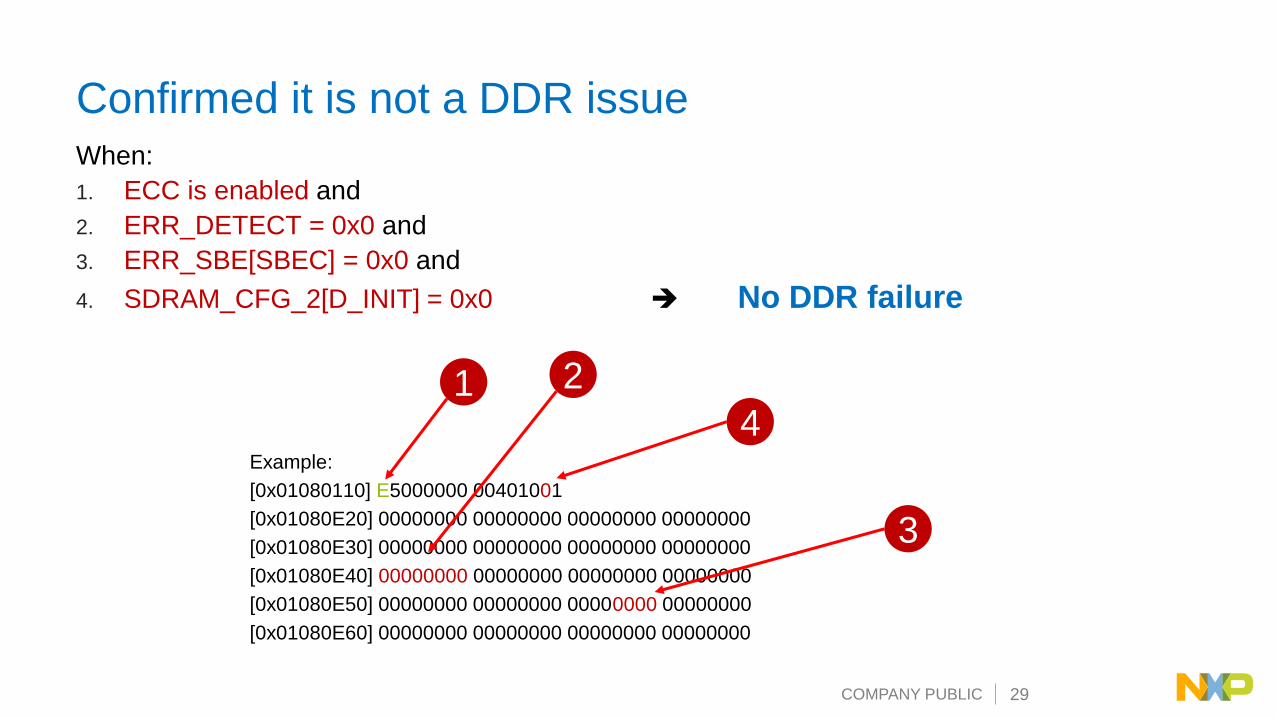
Confirmed it is not a DDR issueWhen:
1. ECC is enabled and
2. ERR_DETECT = 0x0 and
3. ERR_SBE[SBEC] = 0x0 and
4. SDRAM_CFG_2[D_INIT] = 0x0 No DDR failure
Example:
[0x01080110] E5000000 00401001
[0x01080E20] 00000000 00000000 00000000 00000000
[0x01080E30] 00000000 00000000 00000000 00000000
[0x01080E40] 00000000 00000000 00000000 00000000
[0x01080E50] 00000000 00000000 00000000 00000000
[0x01080E60] 00000000 00000000 00000000 00000000
1 2
3
4
COMPANY PUBLIC 30
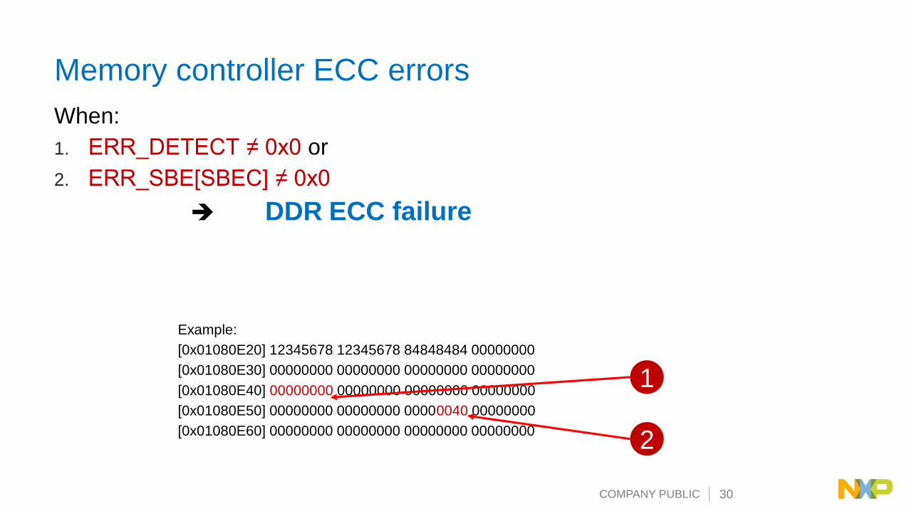
Memory controller ECC errors
When:
1. ERR_DETECT ≠ 0x0 or
2. ERR_SBE[SBEC] ≠ 0x0
DDR ECC failure
Example:
[0x01080E20] 12345678 12345678 84848484 00000000
[0x01080E30] 00000000 00000000 00000000 00000000
[0x01080E40] 00000000 00000000 00000000 00000000
[0x01080E50] 00000000 00000000 00000040 00000000
[0x01080E60] 00000000 00000000 00000000 00000000
1
2

COMPANY PUBLIC 31
How to get ECC register dump via ccs
This is for debug use only.
1) Open a CCS window (C:\Freescale\CW4NET_v2016.01\Common\CCS\bin\ccs.exe)
2) Physical connection: USB to PC, JTAG to the customer board.
3) SW connection: in the ccs window type:
(for LS2088)
delete allconfig cc cwtapccs::config_chain {ls2085a dap}display ccs::read_mem 326 0x1080000 4 0 1024 ccs::write_mem 326 0x1080FB0 4 0 0x10000000 display ccs::read_mem 326 0x1080000 4 0 1024
(for LS1043 or LS1046)
delete allconfig cc cwtapccs::config_chain {ls1043a dap sap2}display ccs::read_mem 32 0x1080000 4 0 1024 ccs::write_mem 32 0x1080FB0 4 0 0x10000000 display ccs::read_mem 32 0x1080000 4 0 1024
(for T1)
delete allconfig cc cwtapccs::config_chain t1040display ccs::read_mem 0 0x30000 0x8000 4 2 1024 ccs::write_mem 0 0x30000 0x8FB0 4 2 0x10000000 display ccs::read_mem 0 0x30000 0x8000 4 2 1024
(for LS1088)
delete allconfig cc cwtapccs::config_chain {ls1088a dap}display ccs::read_mem 119 0x1080000 4 0 1024 ccs::write_mem 119 0x1080FB0 4 0 0x10000000 display ccs::read_mem 119 0x1080000 4 0 1024
(for LS1021A)
delete allconfig cc cwtapccs::config_chain {ls1020a dap sap2}display ccs::read_mem 17 0x1080000 4 0 1024 ccs::write_mem 17 0x1080FB0 4 0 0x10000000display ccs::read_mem 17 0x1080000 4 0 1024
COMPANY PUBLIC 32
LS1024 DDR3 and LS1012 DDR3L
• LS1024:
− DDR3, 32-bit + ECC
− Follows a strict layout policy, any need board design needs to be approved
− Specific register setting will be generated by the factory
• LS1012:
− DDR3L, 16-bit, no ECC
− One chip select
− Only one x16 DRAM or two x8 DRAM
− QCVS will generate settings + simple write-read-compare test

COMPANY PUBLIC 33
CONFIGURATIONS AND
VALIDATION VIA QCVS TOOL
COMPANY PUBLIC 34
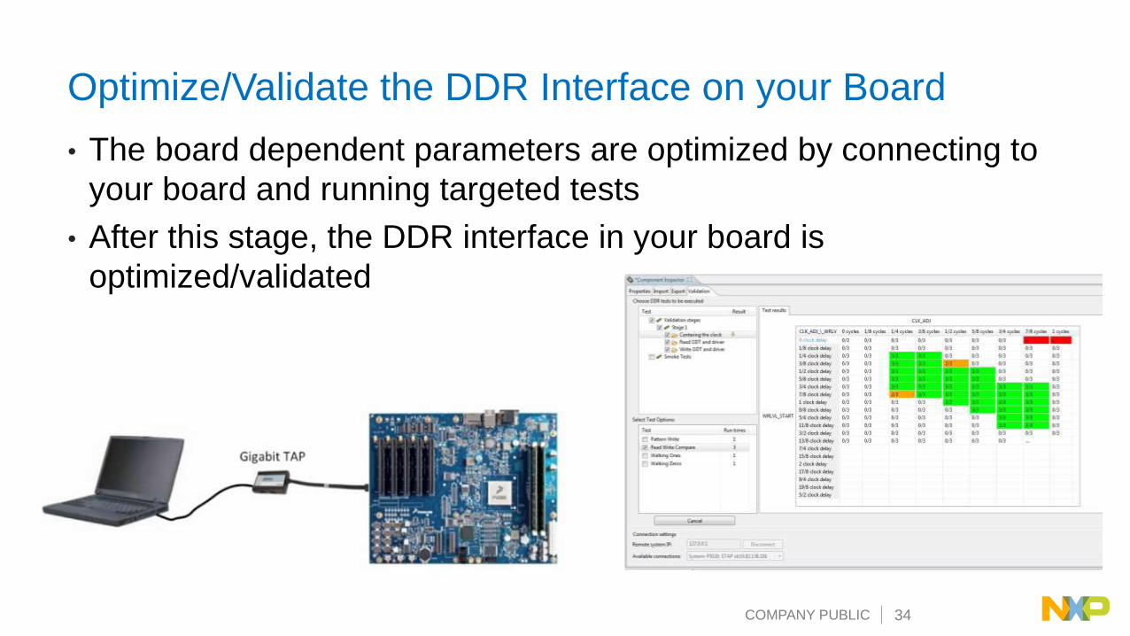
Optimize/Validate the DDR Interface on your Board
• The board dependent parameters are optimized by connecting to
your board and running targeted tests
• After this stage, the DDR interface in your board is
optimized/validated
COMPANY PUBLIC 35
Register Configuration
Two general types of registers to be configured in the memory controller:
• First register type are set to the DRAM related parameter values, that are provided via SPD or DRAM datasheet. Over 100 register fields fall under this category.
• Second register type are the Non-SPD values that are set based on customer’s application. For example:− On-die-termination (ODT) settings for DRAM and controller
− Driver impedance setting for DRAM and controller
− Clock adjust value selection
− Write leveling start value (WRLVL_START)

COMPANY PUBLIC 36
Using QCS DDRv Tool
Configure and optimize your DDR interface in a matter of hours
1. Use the tool to generate the DDR register settings• Use the latest revision
• Select the SPD option in configuration wizard when DIMM is used
• Select Auto Configuration when Discrete DRAM is used
2. Optimize the DDR register setting on your QorIQ board• Run the clock centering test
• Optimize the ODT and drive strength for read and write
DDRv DEMO:
https://www.nxp.com/video/configure-qoriq-ddr-in-3-minutes:QRIQ-DDR-CONFIGURATION
COMPANY PUBLIC 37
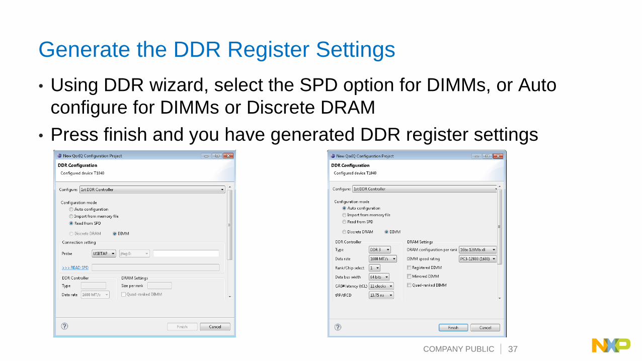
Generate the DDR Register Settings
• Using DDR wizard, select the SPD option for DIMMs, or Auto
configure for DIMMs or Discrete DRAM
• Press finish and you have generated DDR register settings

COMPANY PUBLIC 38
DDR Interface ADD/CMND Bus Margins via QCVS Tool
• Clock signal is stepped cross the address bus eye unit interval and
tool regenerate a pass/fail address bus eye.▪ In the example below the address eye is passing from 1/8 clk to 7/8 of clock. This is 80% of
open eye from maximum available address bus unit interval.
• Write level margin table provides
the reconstruction pass fail
margins for each byte lane.

COMPANY PUBLIC 39
Data Write Cycle
MemoryInterconnects
(Ideal Condition)
Controller
Differential
Strobe
Data
COMPANY PUBLIC 40
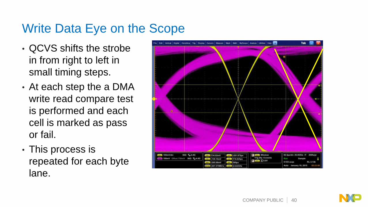
Write Data Eye on the Scope
• QCVS shifts the strobe
in from right to left in
small timing steps.
• At each step the a DMA
write read compare test
is performed and each
cell is marked as pass
or fail.
• This process is
repeated for each byte
lane.
COMPANY PUBLIC 41
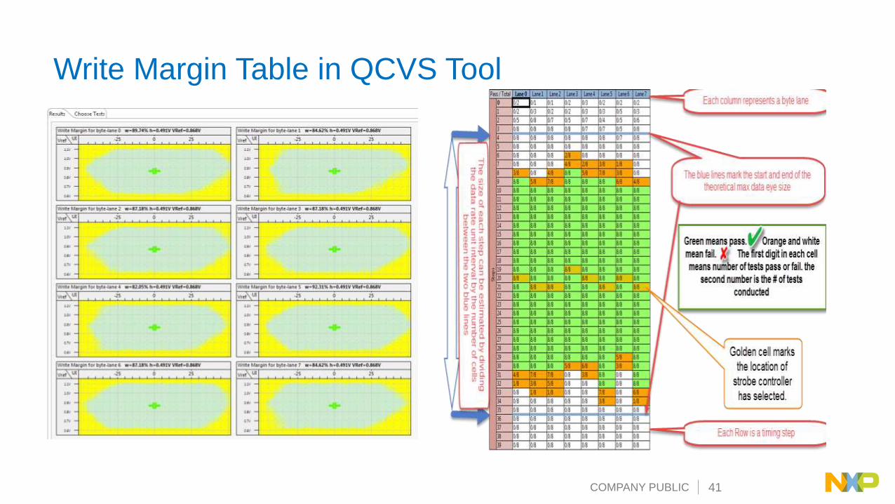
Write Margin Table in QCVS Tool
COMPANY PUBLIC 42
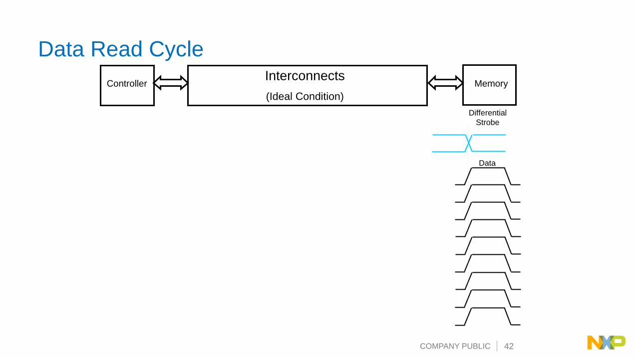
Data Read Cycle
ControllerInterconnects
(Ideal Condition)
Memory
Differential
Strobe
Data
COMPANY PUBLIC 43
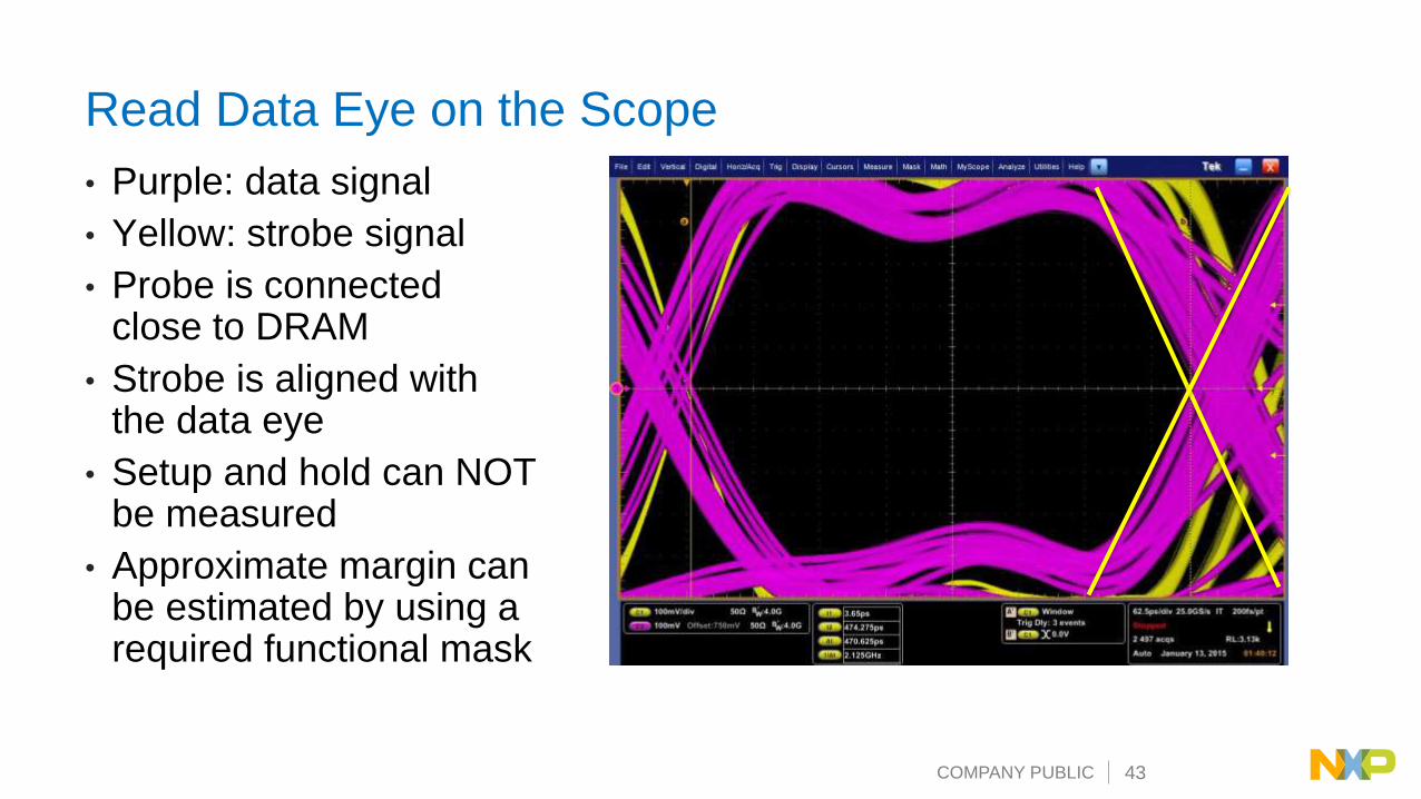
Read Data Eye on the Scope
• Purple: data signal
• Yellow: strobe signal
• Probe is connected close to DRAM
• Strobe is aligned with the data eye
• Setup and hold can NOT be measured
• Approximate margin can be estimated by using a required functional mask
COMPANY PUBLIC 44
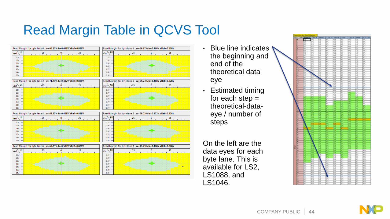
Read Margin Table in QCVS Tool
• Blue line indicates the beginning and end of the theoretical data eye
• Estimated timing for each step = theoretical-data-eye / number of steps
On the left are the data eyes for each byte lane. This is available for LS2, LS1088, and LS1046.
COMPANY PUBLIC 45
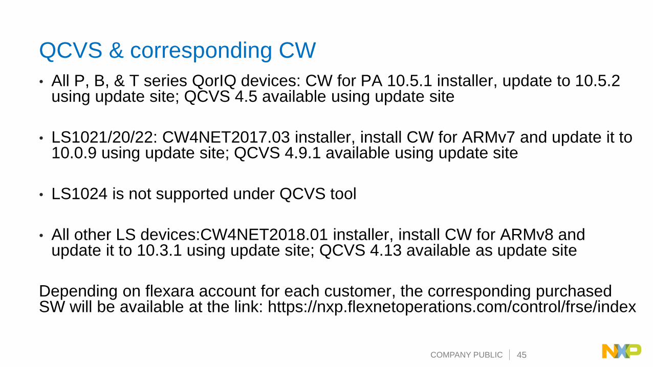
QCVS & corresponding CW
• All P, B, & T series QorIQ devices: CW for PA 10.5.1 installer, update to 10.5.2 using update site; QCVS 4.5 available using update site
• LS1021/20/22: CW4NET2017.03 installer, install CW for ARMv7 and update it to 10.0.9 using update site; QCVS 4.9.1 available using update site
• LS1024 is not supported under QCVS tool
• All other LS devices:CW4NET2018.01 installer, install CW for ARMv8 and update it to 10.3.1 using update site; QCVS 4.13 available as update site
Depending on flexara account for each customer, the corresponding purchased SW will be available at the link: https://nxp.flexnetoperations.com/control/frse/index
COMPANY PUBLIC 46
Summary
Majority of the customer DDR issues can be resolved by:
• Schematics review for any errors
• Verify DRAM reset signal is correct
• Use the QCVS tool to generate and validate DDR
• Verify DQ mapping is correct
• Verify write leveling by entering correct CLK to DQS skew in QCVS
tool

NXP and the NXP logo are trademarks of NXP B.V. All other product or service names are the property of their respective owners. © 2016 NXP B.V.