Embed Size (px)
Citation preview
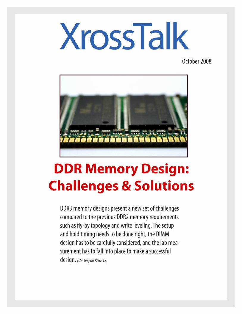
DDR Memory Design: Challenges & Solutions
XrossTalk
DDR3 memory designs present a new set of challenges compared to the previous DDR2 memory requirements such as fly-by topology and write leveling. The setup and hold timing needs to be done right, the DIMM design has to be carefully considered, and the lab mea-surement has to fall into place to make a successful design. (starting on PAGE 12)
October 2008

XrossTalk On the Web
Get the latest issue of XrossTalk Magazine, join the discussions in the forum, read the blogs, find the scoop on what’s happening in the industry, setup your profile to network with your colleagues and make new connections, view our Featured Articles, and much more!
www.xrosstalkmag.com
editor’s
The design of memory systems has continually progressed into a very com-plex approach of balancing multiple trade-offs between cost and features while still meeting your design targets. Remember when you thought first-generation DDR memory was tough to implement? Now we have on-die
termination and write-leveling to contend with to get it all to work.For this month’s issue we tracked down some of the engineers working on
memory designs and got their views on transitioning to DDR3, putting the timing budget together and analyzing the memory design in the lab. (See our feature this month, ‘DDR Memory Design’, pg 12.)
We’ve also made some changes here at XrossTalk going to a more manage-able quarterly publication and we will continue to experiment with new delivery methods and designs to give you, the readers, the most up to date information in the field!
Remember When
Timothy CoyleEditor
4 | XrossTalk Magazine | October 2008
note >>Column Contributors
EDA Insights >> Daniel Payne
Daniel Payne is an EDA marketing consultant who started out with Intel designing DRAMs then moved to EDA companies in roles as AE, technical marketing and product marketing. He lives inOregon, moderates an EDA group at http://eda.plaxogroups.com, blogs at http://www.chipdesignmag.com/payne and has a web site at http://www.marketingeda.com.

XrossTalkOctober 2008 | Volume I | Issue 3
Timothy Coyle
EDITOR
ADVERTISING SALESTimothy Coyle
Editor/Sales(617) 297-2566 | Fax: (207) 510-8099
XrossTalk would like to help you get your product or service in front of the right audience! Contact us to see how we can help your marketing and branding strategies.
PUBLICATION
XrossTalk Magazine is published quarterly each year.
Join the XrossTalk Mailing List!
Join the XrossTalk Magazine mailing list to stay up-to-date on what’s happening with the magazine! You’ll get an email once a month letting you know when the next issue of XrossTalk will be available plus you’ll get a sneak peek at upcoming articles.
Benefits include:Monthly email with updates on XrossTalk Magazine•Updates on events and news in the industry•Discounts and promotions for training events and conferences•Much More !•
To join the XrossTalk Magazine mailing list just click on the envelope above and it will take you directly to the mailing list sign up page. You can also go to www.siconsultant.com/maillist.html.We respect your privacy and your information will not be given to other parties.
Click to Join the XrossTalk Mailing List!
Chip, Package, & PCB Design for Engineers | XrossTalk Magazine | 5
table of contents
feature
Debugging DDR Clock Jitter
Read the guest articles to learn about debugging DDR clock jitter in the lab, squeezing the most out of your setup and hold timing budget, and the new challenges presented by DDR3 DIMM design.
Measurement
Learn from Agilent’s Min Jie Chong on how to debug DDR clock jitter on your next design.
12
DDR Memory Design12
Optimizing DDR3 Timing
Signal Integrity
Sisoft’s Todd Westerhoff shows how to optimize your DDR3 interface to properly account for setup and hold timing.
15
DDR3 Design Challenges
Design
Randy Wolff and Dirgha Khatri from Micron talk about the new design challenges for DDR3 DIMM design.
18
Signal Integrity Companion
Book Review
We review one of Prentice Hall’s latest Signal Integrity books ‘Signal Integrity Engineer’s Companion’.
21
Readers Respond
More Features9
NEXT ISSUE: SerDes DesignHigh speed SerDes design has taken another leap forward with new inter-face technologies like PCI Express Generation 2 topping out at speeds greater than 5 Gbps and we’ll talk to the best and brightest in the field to see how these SerDes designs are being simulated and measured.
6 | XrossTalk Magazine | October 2008
Events & Calendar8
ColumnsEDA Insights10
Get the latest news on what’s happening in the EDA industry today.

Catch Us At PCB Orlando 2008!
There’s something lurking on the horizon ...
HIGHLIGHTS | EVENTS
I attended the Cadence Live conference in San Jose in September and it was a great event. The Cadence Live conference is the user group conference put on by Cadence and features presentations by both Cadence customers and Cadence employees.
I went to all of the high-speed design tracks and below are some of my notes from the event. (You can see my full conference review on my blog called the Busi-ness of Engineering at www.siconsultant.com/blog.)
Sessions: I attended a lot of great sessions (and gave a presentation as well) and below are some of the highlights/themes I picked up on.
* High Speed SerDes interfaces such as PCI Express 2.0 with above 5 Gbps operation is starting to get everyone’s attention. The need to be able to simulate both the channel and the IO to figure out if you meet spec or not is challenging to most designers.
* IBIS-AMI is starting to get traction among designers. Lots of people have heard about but most still do not know how to make the models or how the tools will use them. Hopefully there will be more adoption and information in the next year to help this standard take off.
* Designers are still frustrated at the 3 Gbps range with encrypted SPICE models instead of IBIS. More work needs to be done showing how IBIS can be used at these frequencies with pre-emphasis and other technologies.
* IBIS-AMI is about equalization and the algorithms to open the eye back up at the receiver. Some specs even state that the only way to verify a parameter is through simulation.
* Cadence still has its work cut out for it to get more designers to adopt Constraint Manager into its design flow, especially tying it into SpecctraQuest simulations.
* The Allegro Power Integrity tool can help PCB designers with the power deliv-ery network on their PCB and the upcoming release should address some of the current issues with the tool such as only allowing a static impedance profile.
Events: Cadence did a great job of mixing different networking events through-out the conference along with the vendor exhibits. By far the best event was the poker tournament with poker star Phil Gordon as the MC. I did play and it was a lot of fun!
Overall it was a great conference and I’m looking forward to attending again next year!
Cadence Live Conference Upcoming Events
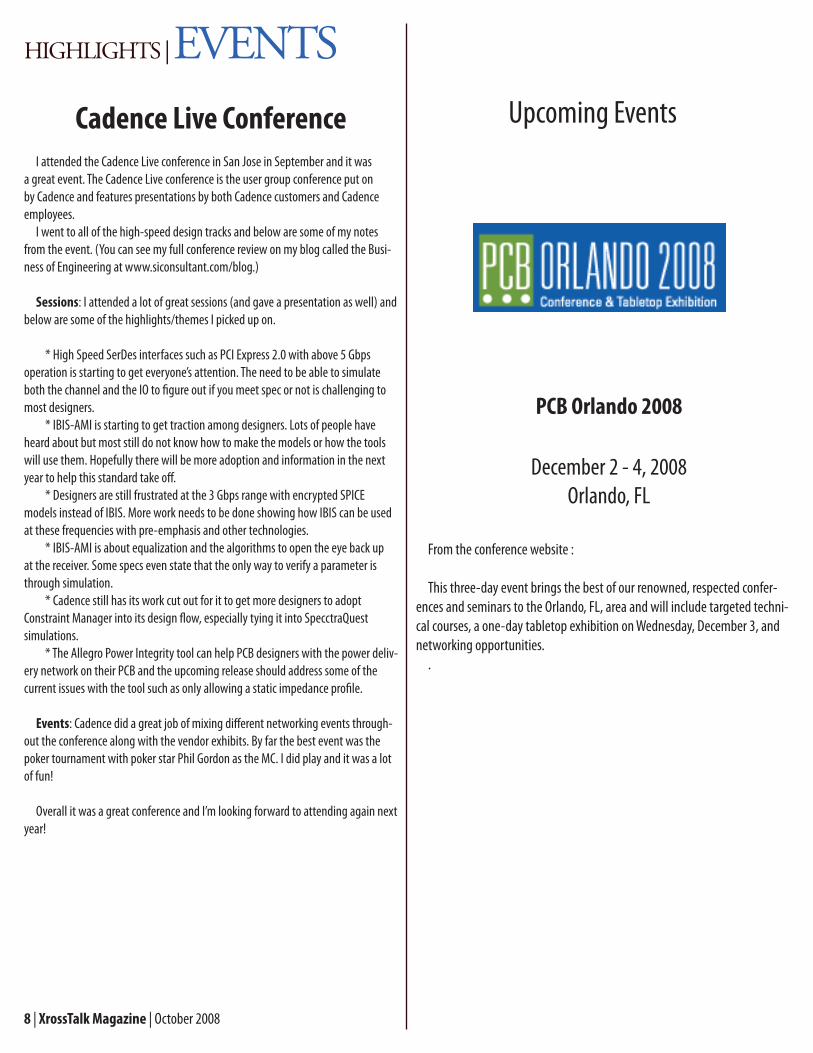
PCB Orlando 2008
December 2 - 4, 2008 Orlando, FL
From the conference website :
This three-day event brings the best of our renowned, respected confer-ences and seminars to the Orlando, FL, area and will include targeted techni-cal courses, a one-day tabletop exhibition on Wednesday, December 3, and networking opportunities.
.
8 | XrossTalk Magazine | October 2008
Chip, Package, & PCB Design for Engineers | XrossTalk Magazine | 9
READERS RESPOND | MAIL
To alert us to an error, send an email to [email protected]. To submit a letter, write to [email protected] or Signal Consulting Group, C/O XrossTalk Magazine, 405 Western Ave #430, South Portland, ME, 04106. Letters may be edited for space and style. Submission constitutes permission to use.
In last months feature we covered the emerging IBIS-AMI modeling standard for high-speed SerDes design that are operating at frequencies above 5 Gbps such as PCI Express Generation 2.
The IBIS Open Forum has now officially ratified the 5.0 IBIS specification that includes support for the IBIS-AMI modeling framework so we should expect to see the major EDA tool vendors add official support for IBIS-AMI in their upcoming releases. This will be a welcome added feature and will help with the simulation and design of these complex SerDes designs. The goal of the IBIS-AMI modeling standard is to provide a universal model format that all of the simulation tools can use and not rely on one proprietary solution.
.
Update
XrossTalk Magazine is looking for your contributions! Would you like to contribute a guest article? Do you want to voice your opinion on a topic? Promote your company and your research by publishing in XrossTalk Maga-zine. Help make XrossTalk Magazine the ‘must read’ for the high speed digital design community!
We are also looking for information on upcoming conference events, new products (both hardware and software), industry news, and other relevant information for the high speed digital design community.
For all inquires, please contact the editor at [email protected] for more information.
The Readers Respond section is your chance to provide feedback and opinions on what you have been reading in XrossTalk Magazine. Like any magazine, XrossTalk will only be valuable to the community if the community is involved. We value your feedback and want to hear from you on what you like and what you don’t like. So let us know what your thoughts are and share your opinions with the rest of the design community by writing a letter to the editor!
Your Feedback
Editorial Team
Looking for Authors!
CadenceI sighed with huge relief on August 15th as Cadence ended their hostile bid for
Mentor. Had this bid gone through we would’ve witnessed the largest layoff in EDA history caused by extreme product overlap and redundant layers of people. I estimated at least 1,000 people would be given walking papers if this ill-fated merger was accepted.
The irony is that Cadence in it’s formative years had a series of absolutely brilliant mergers (SDA and ECAD) and acquisitions (Gateway Design Automation, Tangent). The first signs of faltering corporate thinking began with the acquisition of Valid, which also had extreme product overlap. Valid customers ended up very frustrated because their favorite schematic capture tool was being killed.
Cadence made the typical merger mistake of taking their eye off the ball, sales. Because the Cadence sales force was too busy thinking about who would survive the merger and who would be let go they stopped taking orders which then caused a quarterly loss for the company. CDN stock fell some 30% in one day after they announced lower revenue projections and a loss for the quarter.
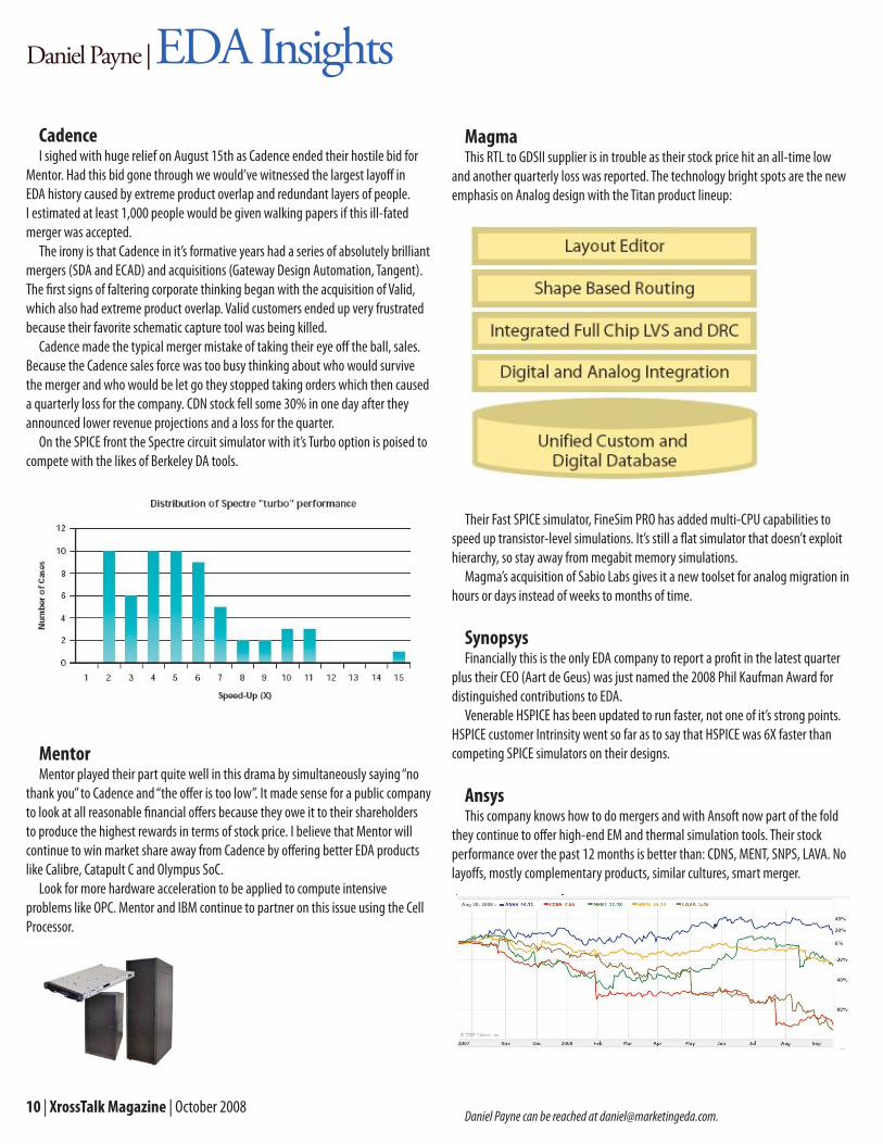
On the SPICE front the Spectre circuit simulator with it’s Turbo option is poised to compete with the likes of Berkeley DA tools.
MentorMentor played their part quite well in this drama by simultaneously saying “no
thank you” to Cadence and “the offer is too low”. It made sense for a public company to look at all reasonable financial offers because they owe it to their shareholders to produce the highest rewards in terms of stock price. I believe that Mentor will continue to win market share away from Cadence by offering better EDA products like Calibre, Catapult C and Olympus SoC.
Look for more hardware acceleration to be applied to compute intensive problems like OPC. Mentor and IBM continue to partner on this issue using the Cell Processor.
10 | XrossTalk Magazine | October 2008
MagmaThis RTL to GDSII supplier is in trouble as their stock price hit an all-time low
and another quarterly loss was reported. The technology bright spots are the new emphasis on Analog design with the Titan product lineup:
Their Fast SPICE simulator, FineSim PRO has added multi-CPU capabilities to speed up transistor-level simulations. It’s still a flat simulator that doesn’t exploit hierarchy, so stay away from megabit memory simulations.
Magma’s acquisition of Sabio Labs gives it a new toolset for analog migration in hours or days instead of weeks to months of time.
SynopsysFinancially this is the only EDA company to report a profit in the latest quarter
plus their CEO (Aart de Geus) was just named the 2008 Phil Kaufman Award for distinguished contributions to EDA.
Venerable HSPICE has been updated to run faster, not one of it’s strong points. HSPICE customer Intrinsity went so far as to say that HSPICE was 6X faster than competing SPICE simulators on their designs.
AnsysThis company knows how to do mergers and with Ansoft now part of the fold
they continue to offer high-end EM and thermal simulation tools. Their stock performance over the past 12 months is better than: CDNS, MENT, SNPS, LAVA. No layoffs, mostly complementary products, similar cultures, smart merger.
Daniel Payne can be reached at [email protected].
Daniel Payne | EDA Insights

Join the XrossTalk Mailing List!
Join the XrossTalk Magazine mailing list to stay up-to-date on what’s happening with the magazine! You’ll get an email once a month letting you know when the next issue of XrossTalk will be available plus you’ll get a sneak peek at upcoming articles.
Benefits include:Monthly email with updates on XrossTalk Magazine•Updates on events and news in the industry•Discounts and promotions for training events and conferences•Much More !•
To join the XrossTalk Magazine mailing list just click on the envelope above and it will take you directly to the mailing list sign up page. You can also go to www.siconsultant.com/maillist.html.We respect your privacy and your information will not be given to other parties.
Click to Join the XrossTalk Mailing List!
Overview
With the data transfer rate of the DDR (Double Data Rate Synchronous Dynamic Random Memory) memory technology increasing rapidly, interoperability is becoming a huge challenge for engineers. Fundamentally, interoperability begins at the physical layer and one of the most critical attribute is the jitter performance of the clock signal. The clock on the DDR interface is transmitted from the memory controller to the DDR chips. It is the reference for all other signals generation on the DDR system, such as the strobe, data, address and command signals. Thus having good clock jitter performance is critical as jitter on the clock will be transferred over to other signals. If the jitter performance on the clock is bad to begin with, jitter issues can be transparent on the other signals as well.
How does jitter affect the performance of the DDR system? Jitter can affect the decision making as it shifts the position of the edge or amplitude of a signal from its ideal position. More jitter causes the position to drift further away from the ideal. With the non-ideal position, the DDR system could be sampling the wrong informa-tion, which would significantly increase the bit error rate of the system. Ultimately, the system will fail to work. This is compounded by the shrinking window validity time of the faster DDR speeds where ever so little of jitter can cause this phenom-enon.
As clock jitter being so essential for interoperability, JEDEC (Joint Electron Devices Engineering Council) has specified a long list of jitter parameters that the clock has to adhere to. The purpose is to ensure the amount of jitter is kept within the tolerable limit so the DDR system communication would not break down. With the specification, you as an engineer are faced with a challenging task of not only ensuring your clock is within the jitter specification but also to debug and find the source of jitter when the clock does not comply with the requirements. This article will highlight some of the available tools and methods in the oscilloscope that can quickly help engineers perform the clock jitter analysis as well as debugging jitter failures. The tools and methods are applicable for DDR 1, 2 and 3.
Automated Clock Jitter Measurement
With the huge list of jitter test specification, making measurement and analyz-ing the clock waveform could be time consuming. On top of that, the jitter needs to be analyzed with very specific requirement. The DDR2 specification, JESD79-2E requires the oscilloscope to be able to analyze multiple cycle-to-cycle jitter measurements over 200 clock cycles. Some of the jitter measurements are tJIT(cc), tERR(2per), tERR(3per), tJIT(duty) and more. Although not mentioned in the speci-fication, the jitter measurements ought to be repeated over a huge number of clock cycles, typically 50 million clock cycles to ensure robustness. With such requirement, it is no wonder you can be faced with a huge task.
Fortunately, there are oscilloscopes which offer DDR compliance test software that provide automated clock measurement and analysis based on the JEDEC speci-fication. All you need is hooking up the clock signal to the oscilloscope, select the clock jitter tests and then run the test. The software then compares the measure-
Analyzing and Debugging DDR Clock Jitter Issues
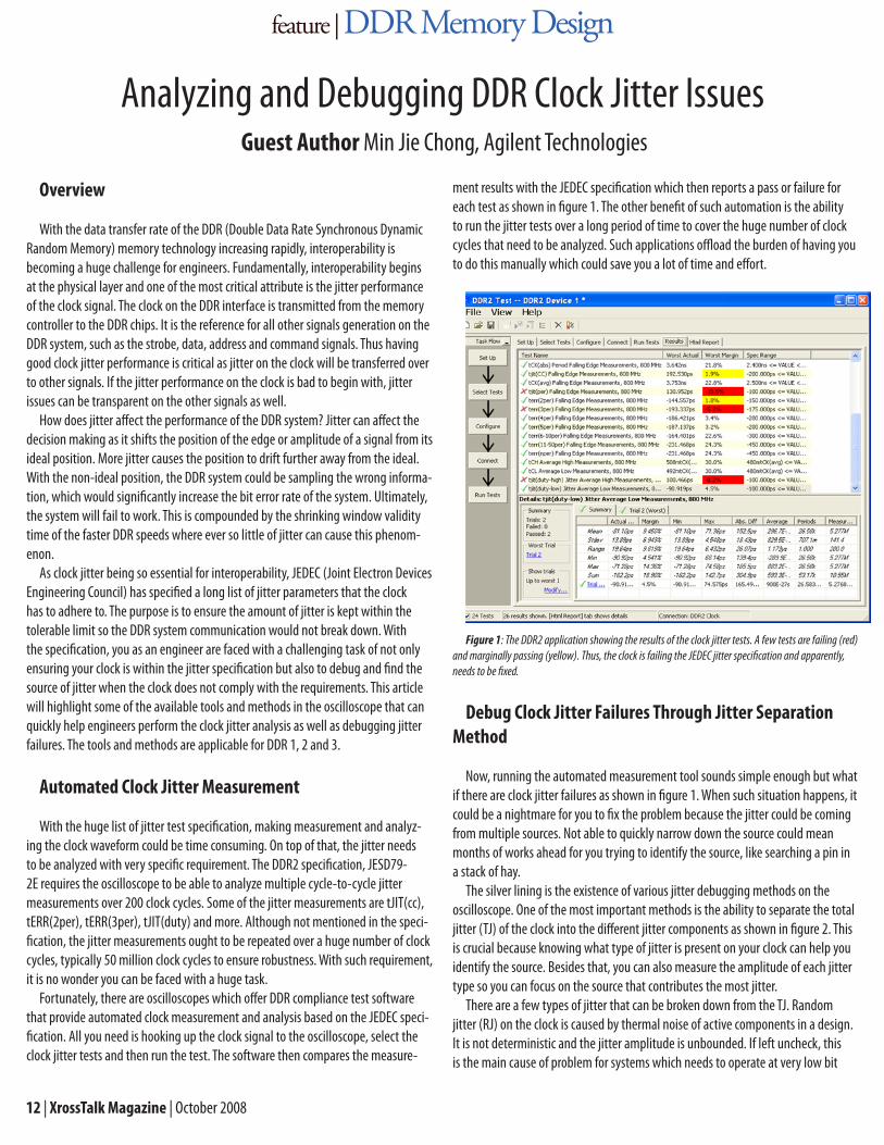
ment results with the JEDEC specification which then reports a pass or failure for each test as shown in figure 1. The other benefit of such automation is the ability to run the jitter tests over a long period of time to cover the huge number of clock cycles that need to be analyzed. Such applications offload the burden of having you to do this manually which could save you a lot of time and effort.
Figure 1: The DDR2 application showing the results of the clock jitter tests. A few tests are failing (red) and marginally passing (yellow). Thus, the clock is failing the JEDEC jitter specification and apparently, needs to be fixed.
Debug Clock Jitter Failures Through Jitter Separation Method
Now, running the automated measurement tool sounds simple enough but what if there are clock jitter failures as shown in figure 1. When such situation happens, it could be a nightmare for you to fix the problem because the jitter could be coming from multiple sources. Not able to quickly narrow down the source could mean months of works ahead for you trying to identify the source, like searching a pin in a stack of hay.
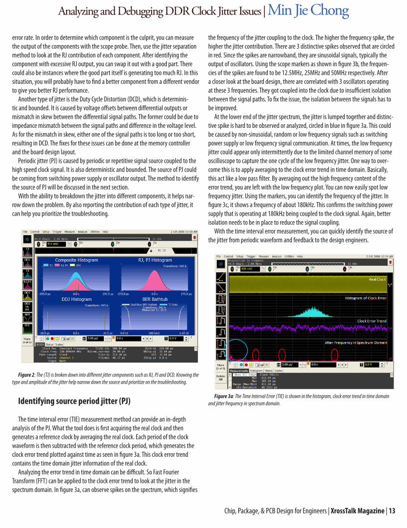
The silver lining is the existence of various jitter debugging methods on the oscilloscope. One of the most important methods is the ability to separate the total jitter (TJ) of the clock into the different jitter components as shown in figure 2. This is crucial because knowing what type of jitter is present on your clock can help you identify the source. Besides that, you can also measure the amplitude of each jitter type so you can focus on the source that contributes the most jitter.
There are a few types of jitter that can be broken down from the TJ. Random jitter (RJ) on the clock is caused by thermal noise of active components in a design. It is not deterministic and the jitter amplitude is unbounded. If left uncheck, this is the main cause of problem for systems which needs to operate at very low bit
Guest Author Min Jie Chong, Agilent Technologies
feature | DDR Memory Design
12 | XrossTalk Magazine | October 2008
Analyzing and Debugging DDR Clock Jitter Issues | Min Jie Chong
Chip, Package, & PCB Design for Engineers | XrossTalk Magazine | 13
error rate. In order to determine which component is the culprit, you can measure the output of the components with the scope probe. Then, use the jitter separation method to look at the RJ contribution of each component. After identifying the component with excessive RJ output, you can swap it out with a good part. There could also be instances where the good part itself is generating too much RJ. In this situation, you will probably have to find a better component from a different vendor to give you better RJ performance.
Another type of jitter is the Duty Cycle Distortion (DCD), which is determinis-tic and bounded. It is caused by voltage offsets between differential outputs or mismatch in skew between the differential signal paths. The former could be due to impedance mismatch between the signal paths and difference in the voltage level. As for the mismatch in skew, either one of the signal paths is too long or too short, resulting in DCD. The fixes for these issues can be done at the memory controller and the board design layout.
Periodic jitter (PJ) is caused by periodic or repetitive signal source coupled to the high speed clock signal. It is also deterministic and bounded. The source of PJ could be coming from switching power supply or oscillator output. The method to identify the source of PJ will be discussed in the next section.
With the ability to breakdown the jitter into different components, it helps nar-row down the problem. By also reporting the contribution of each type of jitter, it can help you prioritize the troubleshooting.
Figure 2: The (TJ) is broken down into different jitter components such as RJ, PJ and DCD. Knowing the type and amplitude of the jitter help narrow down the source and prioritize on the troubleshooting.
Identifying source period jitter (PJ)
The time interval error (TIE) measurement method can provide an in-depth analysis of the PJ. What the tool does is first acquiring the real clock and then generates a reference clock by averaging the real clock. Each period of the clock waveform is then subtracted with the reference clock period, which generates the clock error trend plotted against time as seen in figure 3a. This clock error trend contains the time domain jitter information of the real clock.
Analyzing the error trend in time domain can be difficult. So Fast Fourier Transform (FFT) can be applied to the clock error trend to look at the jitter in the spectrum domain. In figure 3a, can observe spikes on the spectrum, which signifies
the frequency of the jitter coupling to the clock. The higher the frequency spike, the higher the jitter contribution. There are 3 distinctive spikes observed that are circled in red. Since the spikes are narrowband, they are sinusoidal signals, typically the output of oscillators. Using the scope markers as shown in figure 3b, the frequen-cies of the spikes are found to be 12.5MHz, 25MHz and 50MHz respectively. After a closer look at the board design, there are correlated with 3 oscillators operating at these 3 frequencies. They got coupled into the clock due to insufficient isolation between the signal paths. To fix the issue, the isolation between the signals has to be improved.
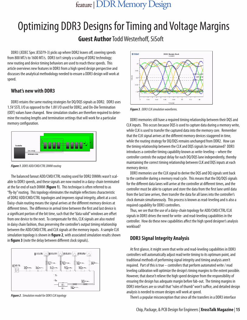
At the lower end of the jitter spectrum, the jitter is lumped together and distinc-tive spike is hard to be observed or analyzed, circled in blue in figure 3a. This could be caused by non-sinusoidal, random or low frequency signals such as switching power supply or low frequency signal communication. At times, the low frequency jitter could appear only intermittently due to the limited channel memory of some oscilloscope to capture the one cycle of the low frequency jitter. One way to over-come this is to apply averaging to the clock error trend in time domain. Basically, this act like a low pass filter. By averaging out the high frequency content of the error trend, you are left with the low frequency plot. You can now easily spot low frequency jitter. Using the markers, you can identify the frequency of the jitter. In figure 3c, it shows a frequency of about 180kHz. This confirms the switching power supply that is operating at 180kHz being coupled to the clock signal. Again, better isolation needs to be in place to reduce the signal coupling.
With the time interval error measurement, you can quickly identify the source of the jitter from periodic waveform and feedback to the design engineers.
Figure 3a: The Time Interval Error (TIE) is shown in the histogram, clock error trend in time domain and jitter frequency in spectrum domain.
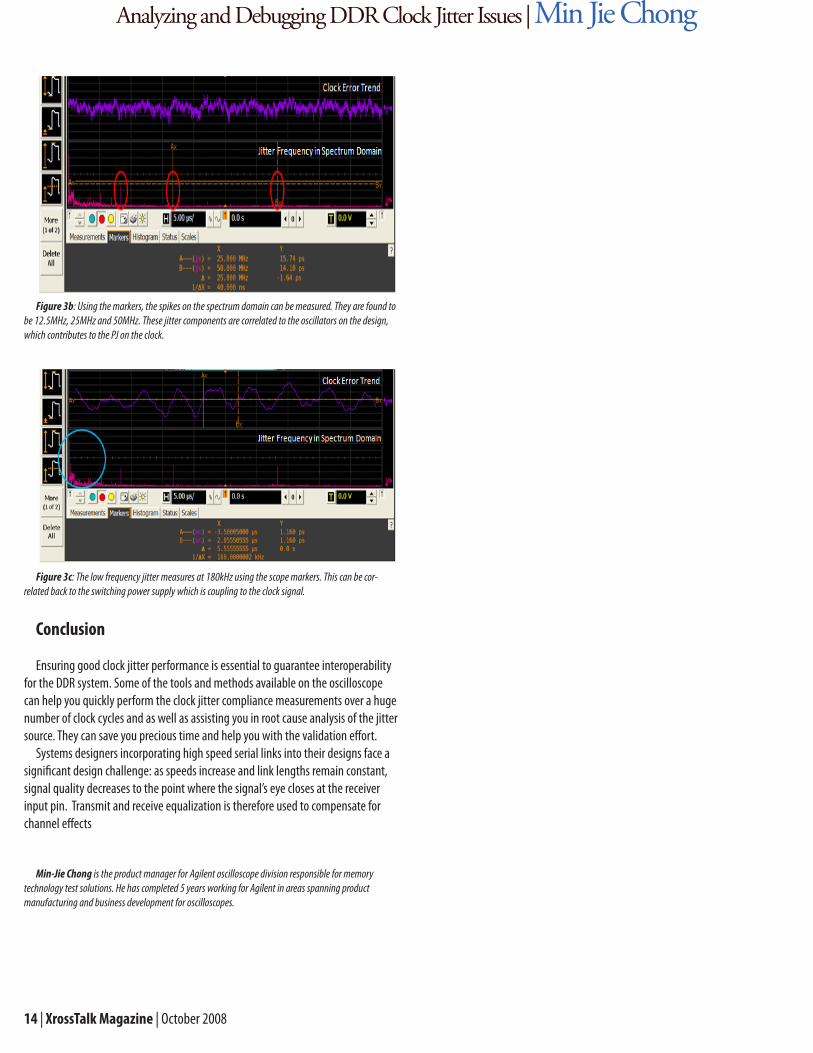
Figure 3b: Using the markers, the spikes on the spectrum domain can be measured. They are found to be 12.5MHz, 25MHz and 50MHz. These jitter components are correlated to the oscillators on the design, which contributes to the PJ on the clock.
Figure 3c: The low frequency jitter measures at 180kHz using the scope markers. This can be cor-related back to the switching power supply which is coupling to the clock signal.
Conclusion
Ensuring good clock jitter performance is essential to guarantee interoperability for the DDR system. Some of the tools and methods available on the oscilloscope can help you quickly perform the clock jitter compliance measurements over a huge number of clock cycles and as well as assisting you in root cause analysis of the jitter source. They can save you precious time and help you with the validation effort.
Systems designers incorporating high speed serial links into their designs face a significant design challenge: as speeds increase and link lengths remain constant, signal quality decreases to the point where the signal’s eye closes at the receiver input pin. Transmit and receive equalization is therefore used to compensate for channel effects
Min-Jie Chong is the product manager for Agilent oscilloscope division responsible for memory technology test solutions. He has completed 5 years working for Agilent in areas spanning product manufacturing and business development for oscilloscopes.
14 | XrossTalk Magazine | October 2008
Analyzing and Debugging DDR Clock Jitter Issues | Min Jie Chong
Chip, Package, & PCB Design for Engineers | XrossTalk Magazine | 15
DDR3 (JEDEC Spec JESD79-3) picks up where DDR2 leaves off, covering speeds from 800 MT/s to 1600 MT/s. DDR3 isn’t simply a scaling of DDR2 technology; new routing and device timing behaviors are used to reach these speeds. This article overviews new features in DDR3 from a high speed design perspective and discusses the analytical methodology needed to ensure a DDR3 design will work at speed.
What’s new with DDR3
DDR3 retains the same routing strategies for DQ/DQS signals as DDR2. DDR3 uses 1.5V SSTL I/O as opposed to the 1.8V I/O used for DDR2, and On-Die Termination (ODT) values have changed. New simulation studies are therefore required to deter-mine the routing lengths and termination settings that will work for a particular memory configuration.
Figure 1. DDR3 ADD/CMD/CTRL DIMM routing
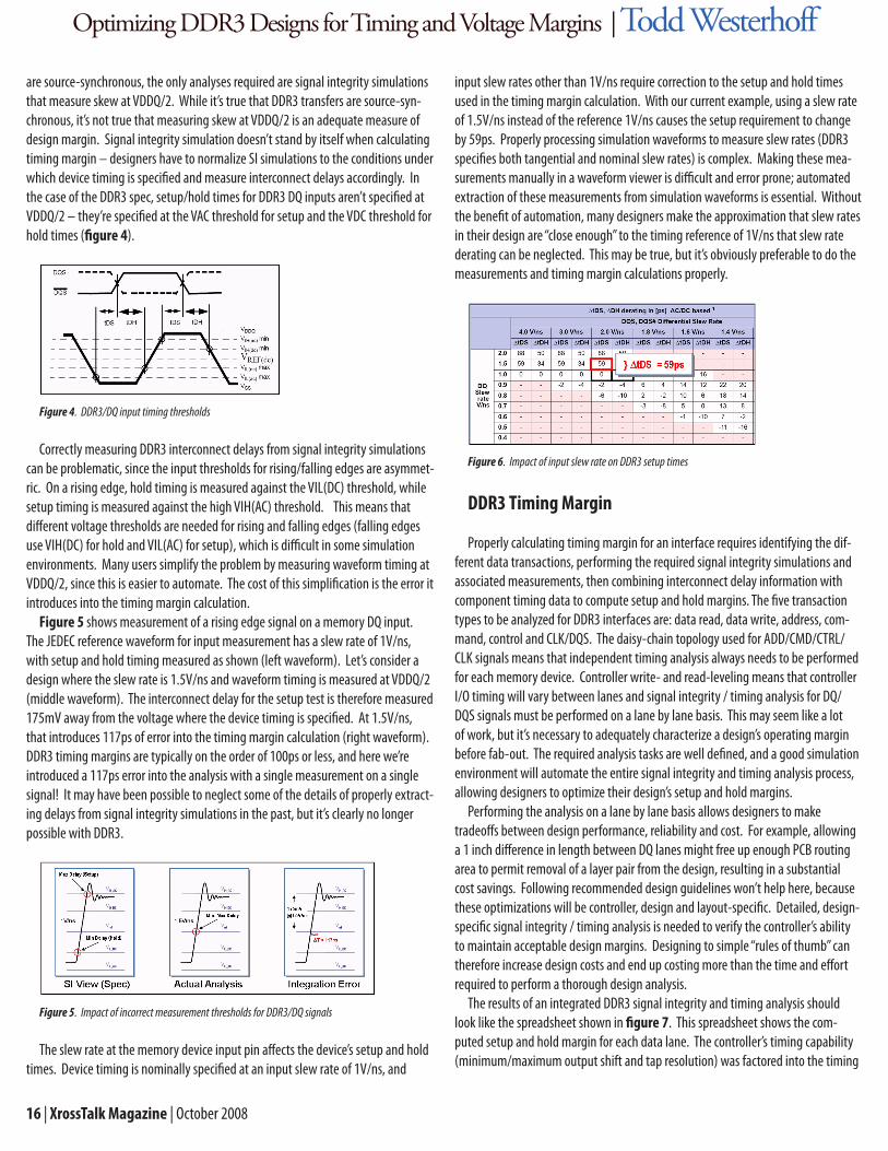
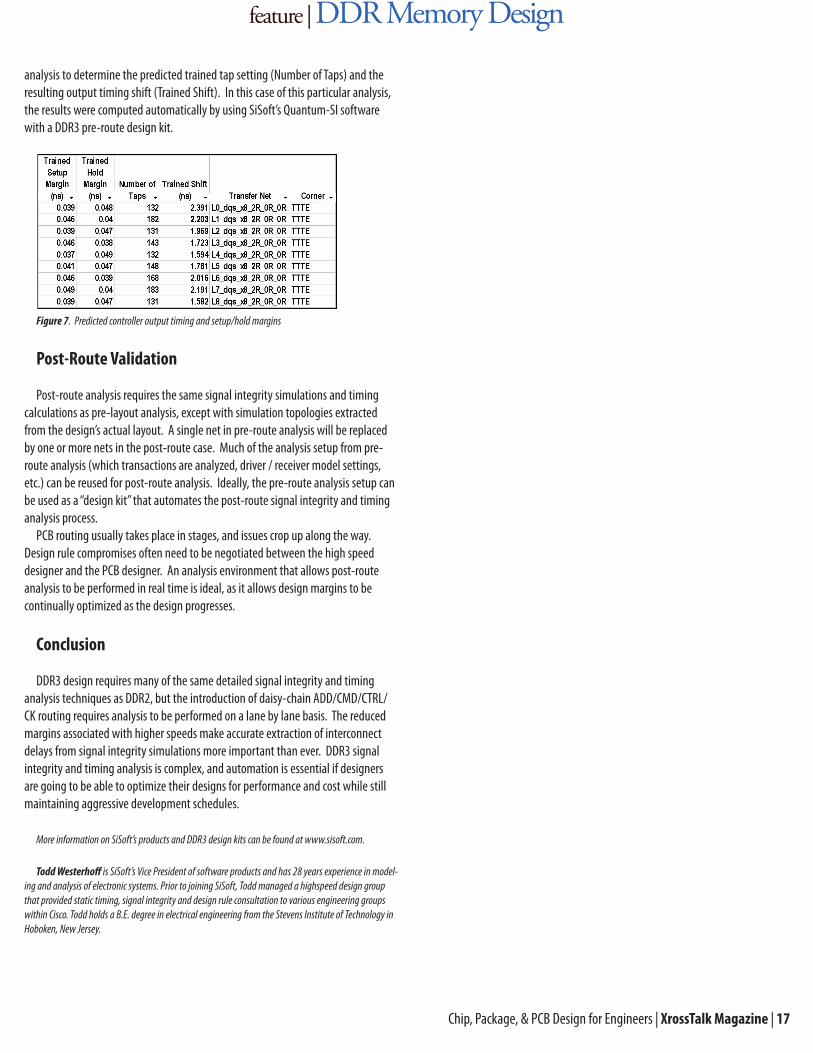
The balanced fanout ADD/CMD/CTRL routing used for DDR2 DIMMs wasn’t scal-able to DDR3 speeds, and these signals are now routed in a daisy-chain terminated at the far end of each DIMM (figure 1). This technique is often referred to as “fly-by” routing. This topology eliminates the multiple reflections characteristic of DDR2 ADD/CMD/CTRL topologies and improves signal integrity, albeit at a cost. Daisy-chain routing means the signal arrives at the different memory devices at different times. The difference in arrival time between the first and last device is a significant portion of the bit time, such that the “data valid” windows are offset from one device to the next. To compensate for this, CLK signals are also routed in daisy chain fashion, thus preserving the controller’s output timing relationship between the ADD/CMD/CTRL and CLK signals at the memory inputs. A sample CLK simulation topology is shown in figure 2, with associated simulation results shown in figure 3 (note the delay between different clock signals).
Figure 2 . Simulation model for DDR3 CLK topology
Optimizing DDR3 Designs for Timing and Voltage Margins
feature | DDR Memory Design
Guest Author Todd Westerhoff, SiSoft
Figure 3. DDR3 CLK simulation waveforms.
DDR3 memories still have a required timing relationship between their DQS and CLK inputs. This occurs because DQS is used to capture data during a memory write, while CLK is used to transfer the captured data into the memory core. Remember that the CLK signal arrives at the different memory devices staggered in time, while the routing strategy for DQ/DQS remains unchanged from DDR2. How can the timing relationship between the CLK and DQS signals be maintained? DDR3 introduces a controller timing capability known as write-leveling – where the controller controls the output delay for each DQ/DQS lane independently, thereby maintaining the correct timing relationship between CLK and DQS inputs at each memory device.
DDR3 memories use the CLK signal to derive the DQS and DQ signals sent back to the controller during a memory read cycle. This means that the DQ/DQS signals for the different data lanes will arrive at the controller at different times, and the controller must be able to capture and store the data from the first lane until data from the last lane arrives, then transfer the data for all lanes into the controller’s clock domain simultaneously. This process is known as read-leveling and is also a required capability for DDR3 controllers.
Thus, we see that the use of a daisy-chain topology for ADD/CMD/CTRL/CLK signals in DDR3 drives the need for write- and read-leveling capabilities in the controller. How do these new capabilities affect the high speed designer’s analysis workload?
DDR3 Signal Integrity Analysis
At first glance, it might seem that write and read-leveling capabilities in DDR3 controllers will automatically adjust read/write timing to its optimum point, and traditional methods of performing signal integrity and timing analysis aren’t required. Part of this is true – controllers that perform automated write / read leveling calibration will optimize the design’s timing margins to the extent possible. However, that doesn’t relieve the high speed designer from the responsibility of ensuring the design has adequate margin before fab-out. The timing margins in DDR3 interfaces are so small that “rules of thumb” won’t suffice, and detailed design analysis is needed to ensure designs will work at speed.
There’s a popular misconception that since all the transfers in a DDR3 interface
Optimizing DDR3 Designs for Timing and Voltage Margins | Todd Westerhoff
16 | XrossTalk Magazine | October 2008
are source-synchronous, the only analyses required are signal integrity simulations that measure skew at VDDQ/2. While it’s true that DDR3 transfers are source-syn-chronous, it’s not true that measuring skew at VDDQ/2 is an adequate measure of design margin. Signal integrity simulation doesn’t stand by itself when calculating timing margin – designers have to normalize SI simulations to the conditions under which device timing is specified and measure interconnect delays accordingly. In the case of the DDR3 spec, setup/hold times for DDR3 DQ inputs aren’t specified at VDDQ/2 – they’re specified at the VAC threshold for setup and the VDC threshold for hold times (figure 4).
Figure 4. DDR3/DQ input timing thresholds
Correctly measuring DDR3 interconnect delays from signal integrity simulations can be problematic, since the input thresholds for rising/falling edges are asymmet-ric. On a rising edge, hold timing is measured against the VIL(DC) threshold, while setup timing is measured against the high VIH(AC) threshold. This means that different voltage thresholds are needed for rising and falling edges (falling edges use VIH(DC) for hold and VIL(AC) for setup), which is difficult in some simulation environments. Many users simplify the problem by measuring waveform timing at VDDQ/2, since this is easier to automate. The cost of this simplification is the error it introduces into the timing margin calculation.
Figure 5 shows measurement of a rising edge signal on a memory DQ input. The JEDEC reference waveform for input measurement has a slew rate of 1V/ns, with setup and hold timing measured as shown (left waveform). Let’s consider a design where the slew rate is 1.5V/ns and waveform timing is measured at VDDQ/2 (middle waveform). The interconnect delay for the setup test is therefore measured 175mV away from the voltage where the device timing is specified. At 1.5V/ns, that introduces 117ps of error into the timing margin calculation (right waveform). DDR3 timing margins are typically on the order of 100ps or less, and here we’re introduced a 117ps error into the analysis with a single measurement on a single signal! It may have been possible to neglect some of the details of properly extract-ing delays from signal integrity simulations in the past, but it’s clearly no longer possible with DDR3.
Figure 5. Impact of incorrect measurement thresholds for DDR3/DQ signals
The slew rate at the memory device input pin affects the device’s setup and hold times. Device timing is nominally specified at an input slew rate of 1V/ns, and
input slew rates other than 1V/ns require correction to the setup and hold times used in the timing margin calculation. With our current example, using a slew rate of 1.5V/ns instead of the reference 1V/ns causes the setup requirement to change by 59ps. Properly processing simulation waveforms to measure slew rates (DDR3 specifies both tangential and nominal slew rates) is complex. Making these mea-surements manually in a waveform viewer is difficult and error prone; automated extraction of these measurements from simulation waveforms is essential. Without the benefit of automation, many designers make the approximation that slew rates in their design are “close enough” to the timing reference of 1V/ns that slew rate derating can be neglected. This may be true, but it’s obviously preferable to do the measurements and timing margin calculations properly.
Figure 6. Impact of input slew rate on DDR3 setup times
DDR3 Timing Margin
Properly calculating timing margin for an interface requires identifying the dif-ferent data transactions, performing the required signal integrity simulations and associated measurements, then combining interconnect delay information with component timing data to compute setup and hold margins. The five transaction types to be analyzed for DDR3 interfaces are: data read, data write, address, com-mand, control and CLK/DQS. The daisy-chain topology used for ADD/CMD/CTRL/CLK signals means that independent timing analysis always needs to be performed for each memory device. Controller write- and read-leveling means that controller I/O timing will vary between lanes and signal integrity / timing analysis for DQ/DQS signals must be performed on a lane by lane basis. This may seem like a lot of work, but it’s necessary to adequately characterize a design’s operating margin before fab-out. The required analysis tasks are well defined, and a good simulation environment will automate the entire signal integrity and timing analysis process, allowing designers to optimize their design’s setup and hold margins.
Performing the analysis on a lane by lane basis allows designers to make tradeoffs between design performance, reliability and cost. For example, allowing a 1 inch difference in length between DQ lanes might free up enough PCB routing area to permit removal of a layer pair from the design, resulting in a substantial cost savings. Following recommended design guidelines won’t help here, because these optimizations will be controller, design and layout-specific. Detailed, design-specific signal integrity / timing analysis is needed to verify the controller’s ability to maintain acceptable design margins. Designing to simple “rules of thumb” can therefore increase design costs and end up costing more than the time and effort required to perform a thorough design analysis.
The results of an integrated DDR3 signal integrity and timing analysis should look like the spreadsheet shown in figure 7. This spreadsheet shows the com-puted setup and hold margin for each data lane. The controller’s timing capability (minimum/maximum output shift and tap resolution) was factored into the timing
Chip, Package, & PCB Design for Engineers | XrossTalk Magazine | 17
analysis to determine the predicted trained tap setting (Number of Taps) and the resulting output timing shift (Trained Shift). In this case of this particular analysis, the results were computed automatically by using SiSoft’s Quantum-SI software with a DDR3 pre-route design kit.
Figure 7. Predicted controller output timing and setup/hold margins
Post-Route Validation
Post-route analysis requires the same signal integrity simulations and timing calculations as pre-layout analysis, except with simulation topologies extracted from the design’s actual layout. A single net in pre-route analysis will be replaced by one or more nets in the post-route case. Much of the analysis setup from pre-route analysis (which transactions are analyzed, driver / receiver model settings, etc.) can be reused for post-route analysis. Ideally, the pre-route analysis setup can be used as a “design kit” that automates the post-route signal integrity and timing analysis process.
PCB routing usually takes place in stages, and issues crop up along the way. Design rule compromises often need to be negotiated between the high speed designer and the PCB designer. An analysis environment that allows post-route analysis to be performed in real time is ideal, as it allows design margins to be continually optimized as the design progresses.
Conclusion
DDR3 design requires many of the same detailed signal integrity and timing analysis techniques as DDR2, but the introduction of daisy-chain ADD/CMD/CTRL/CK routing requires analysis to be performed on a lane by lane basis. The reduced margins associated with higher speeds make accurate extraction of interconnect delays from signal integrity simulations more important than ever. DDR3 signal integrity and timing analysis is complex, and automation is essential if designers are going to be able to optimize their designs for performance and cost while still maintaining aggressive development schedules.
More information on SiSoft’s products and DDR3 design kits can be found at www.sisoft.com.
Todd Westerhoff is SiSoft’s Vice President of software products and has 28 years experience in model-ing and analysis of electronic systems. Prior to joining SiSoft, Todd managed a highspeed design group that provided static timing, signal integrity and design rule consultation to various engineering groups within Cisco. Todd holds a B.E. degree in electrical engineering from the Stevens Institute of Technology in Hoboken, New Jersey.
feature | DDR Memory Design
18 | XrossTalk Magazine | October 2008
Background
DDR3 SDRAM is the third generation of the DDR family of memory technologies. DDR3 bit rates cover 800 Mb/s to 1600 Mb/s and beyond. The increased bandwidth over DDR2 is made possible by features such as DDR3’s 8 bit pre-fetch architecture as compared to DDR2’s 4 bit pre-fetch, lower operating voltage of 1.5 V instead of 1.8 V, and changes to the driver impedances and On-Die Termination (ODT) schemes.
The enhanced features of DDR3 improve system data rates while mitigating pow-er increases. This also means new Signal Integrity (SI) design challenges related to ODT schemes, higher bit rates and timing skew. When DDR3 was first introduced, it was specified to operate up to a 1600 Mb/s data rate in a two slot system. Numer-ous simulations by JEDEC member companies including Micron showed that data nets were the limiting factor to hitting the 1600 Mb/s design target for two slots. DIMM design is currently focused on 1333 Mb/s operation in a two slot system.
Signal Topologies
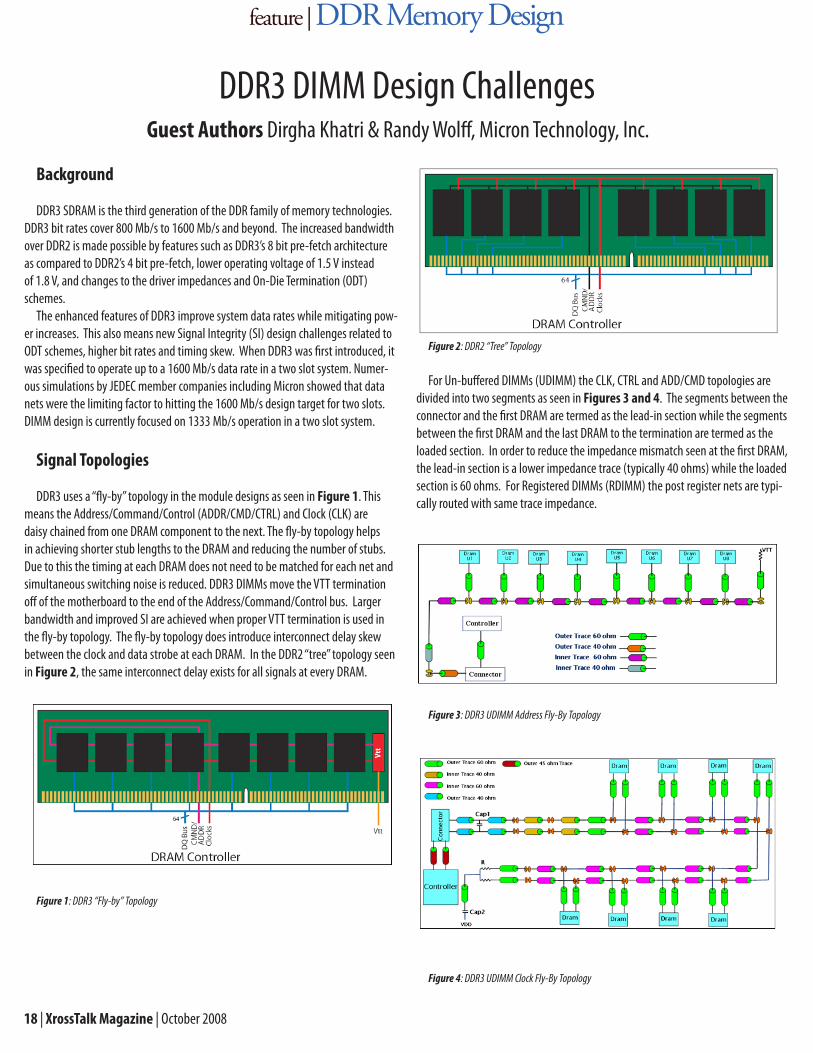
DDR3 uses a “fly-by” topology in the module designs as seen in Figure 1. This means the Address/Command/Control (ADDR/CMD/CTRL) and Clock (CLK) are daisy chained from one DRAM component to the next. The fly-by topology helps in achieving shorter stub lengths to the DRAM and reducing the number of stubs. Due to this the timing at each DRAM does not need to be matched for each net and simultaneous switching noise is reduced. DDR3 DIMMs move the VTT termination off of the motherboard to the end of the Address/Command/Control bus. Larger bandwidth and improved SI are achieved when proper VTT termination is used in the fly-by topology. The fly-by topology does introduce interconnect delay skew between the clock and data strobe at each DRAM. In the DDR2 “tree” topology seen in Figure 2, the same interconnect delay exists for all signals at every DRAM.
Figure 1: DDR3 “Fly-by” Topology
Figure 2: DDR2 “Tree” Topology
For Un-buffered DIMMs (UDIMM) the CLK, CTRL and ADD/CMD topologies are divided into two segments as seen in Figures 3 and 4. The segments between the connector and the first DRAM are termed as the lead-in section while the segments between the first DRAM and the last DRAM to the termination are termed as the loaded section. In order to reduce the impedance mismatch seen at the first DRAM, the lead-in section is a lower impedance trace (typically 40 ohms) while the loaded section is 60 ohms. For Registered DIMMs (RDIMM) the post register nets are typi-cally routed with same trace impedance.
Figure 3: DDR3 UDIMM Address Fly-By Topology
Figure 4: DDR3 UDIMM Clock Fly-By Topology
feature | DDR Memory Design
DDR3 DIMM Design ChallengesGuest Authors Dirgha Khatri & Randy Wolff, Micron Technology, Inc.
Chip, Package, & PCB Design for Engineers | XrossTalk Magazine | 19
The improved SI advantage of the DDR3 fly-by topology over the DDR2 tree topology can be clearly seen in the frequency domain as shown in Figure 5. The frequency response of the fly-by topology exhibits a much wider bandwidth than the tree topology. This translates to higher frequency operation than the tree topol-ogy.
Figure 5: Typical Frequency Response
On-Die Termination (ODT)
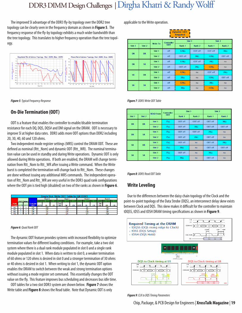
ODT is a feature that enables the controller to enable/disable termination resistance for each DQ, DQS, DQS# and DM signal on the DRAM. ODT is necessary to improve SI at higher data rates. DDR3 adds more ODT options than DDR2 including 20, 30, 40, 60 and 120 ohms.
Two independent mode register settings (MRS) control the DRAM ODT. These are defined as nominal (Rtt_Nom) and dynamic ODT (Rtt_WR). The nominal termina-tion value can be used in standby and during Write operations. Dynamic ODT is only allowed during Write operations. If both are enabled, the DRAM will change termi-nation from Rtt_Nom to Rtt_WR after issuing a Write command. When the Write burst is completed the termination will change back to Rtt_Nom. These changes are done without issuing any additional MRS commands. The independent opera-tion of Rtt_Nom and Rtt_WR are very useful in the DDR3 quad rank configurations where the ODT pin is tied high (disabled) on two of the ranks as shown in Figure 6.
Figure 6: Quad Rank ODT
The dynamic ODT feature provides systems with increased flexibility to optimize termination values for different loading conditions. For example, take a two slot system where there is a dual rank module populated in slot 0 and a single rank module populated in slot 1. When data is written to slot 0, a weaker termination of 60 ohms or 120 ohms is desired in slot 0 and a stronger termination of 30 ohms or 40 ohms is desired in slot 1. When writing to slot 1, the dynamic ODT option enables the DRAM to switch between the weak and strong termination options without issuing a mode register set command. This essentially changes the ODT value on the fly. This feature improves bus scheduling and decreases bus idle time.
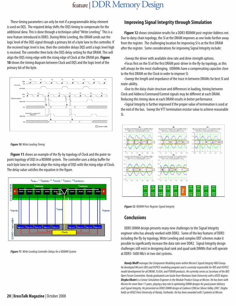
ODT tables for a two slot DDR3 system are shown below. Figure 7 shows the Write table and Figure 8 shows the Read table. Note that Dynamic ODT is only
applicable to the Write operation.
Figure 7: DDR3 Write ODT Table
Figure 8: DDR3 Read ODT Table
Write Leveling
Due to the differences between the daisy chain topology of the Clock and the point-to-point topology of the Data Strobe (DQS), an interconnect delay skew exists between Clock and DQS. This skew makes it difficult for the controller to maintain tDQSS, tDSS and tDSH DRAM timing specifications as shown in Figure 9.
Figure 9: CLK to DQS Timing Parameters
DDR3 DIMM Design Challenges | Dirgha Khatri & Randy Wolff
20 | XrossTalk Magazine | October 2008
These timing parameters can only be met if a programmable delay element is used on DQS. The required delay shifts the DQS timing to compensate for the additional skew. This is done through a technique called “Write Leveling.” This is a new feature introduced in DDR3. During Write Leveling, the DRAM sends out the logic level of the DQS signal through a primary bit of a byte lane to the controller. If the received logic level is low, then the controller delays DQS until a logic level high is received. The controller then locks the DQS delay setting for that DRAM. This will align the DQS rising edge with the rising edge of Clock at the DRAM pin. Figure 10 shows the timing diagram between Clock and DQS and the logic level of the primary bit of the byte.
Figure 10: Write Leveling Timing
Figure 11 shows an example of the fly-by topology of Clock and the point-to-point topology of DQS in a RDIMM system. The controller uses a delay buffer for each byte lane in order to align the rising edge of DQS with the rising edge of Clock. The delay value satisfies the equation in the figure.
Figure 11: Write Leveling Controller Delays for a RDIMM System
Improving Signal Integrity through Simulation
Figure 12 shows simulation results for a DDR3 RDIMM post-register Address net. Due to daisy chain topology, the SI at the DRAM improves as one looks further away from the register. The challenging location for improving SI is at the first DRAM after the register. Some considerations for improving Signal Integrity include:
•Sweepthedriverwithavailableslewrateanddrivestrengthoptions.•FocusfirstontheSIofthefirstDRAMpost-driverinthefly-bytopology,asthis
will always be the most challenging. UDIMMs have a compensating capacitor close to the first DRAM on the Clock in order to improve SI. •SweepthelengthandimpedanceofthetraceinbetweenDRAMsforbestSIand
route-ability. •Duetothedaisychainstructureanddifferencesinloading,timingbetween
Clock and Address/Command/Control signals may be different at each DRAM. Reducing this timing skew at each DRAM results in better performance.•SignalIntegrityisfurtherimprovedifthepropervalueofterminationisusedat
the end of the bus. Sweep the VTT termination resistor value to achieve reasonable SI.
Figure 12: RDIMM Post-Register Signal Integrity
Conclusions
DDR3 DIMM design presents many new challenges to the Signal Integrity engineer who has already worked with DDR2. Some of the key features of DDR3 including the fly-by topology, Write Leveling and complex ODT schemes make it possible to significantly increase the data rate over DDR2. Signal Integrity design challenges still exist in designing dual rank and quad rank DIMMs that will operate at DDR3-1600 Mb/s in two slot systems.
Randy Wolff manages the Component Modeling team within Micron’s Signal Integrity R&D Group. He developed Micron’s IBIS and HSPICE modeling program and is currently responsible for IBIS and HSPICE model development for all DRAM, FLASH, and PSRAM products. He currently serves as Secretary of the IBIS Open Forum Committee. Randy graduated cum laude from Montana State University with a BSEE degree. Dirgha Khatri is a Senior Simulation Engineer in the Module Product Group at Micron. He has been with Micron for more than 11 years, playing a key role in optimizing DIMM designs for good power delivery and Signal Integrity. He presented on DDR3 DIMM design at Cadence CDNLive Silicon Valley 2007. Dirgha holds an MSEE from University of Alaska, Fairbanks. He has been awarded with 5 patents at Micron.
feature | DDR Memory Design

Chip, Package, & PCB Design for Engineers | XrossTalk Magazine | 21
I had a chance recently to review a new book from the Prentice Hall Modern Semiconductor Design Series called A Signal Integrity Engineer’s Companion: Real-Time Test and Measurement and Design Simulation by Geoff Lawday, David Ireland, and Greg Edlund. This book mixes signal integrity simulation with real-time measurement to provide a complete development flow for a product design. Often times these two subjects are separate books by themselves so I found it very help-ful to have them combined into one useful resource.
The first couple of chapters really cover the use of simulation and analysis techniques for performing signal integ-rity analysis on an interface. Greg Edlund provides an excellent introduction to chip-to-chip timing and how to put it all together using simulations. Then there is a full chapter devoted to a DDR2 example that provides examples of how to setup different read and write simulations and put together a timing budget to validate setup and hold times. This chapter alone is worth the price of the book and includes a lot of important details on how to deal with a source synchronous design such as DDR2 memory.
The next section of the book digs deep into the measurement aspect of a product design and is the next logical step from running your design simulations: bring-ing up and validating your design in the lab. The authors cover a lot of ground in the remaining chapters and start with the most important: probing. Often times
New Book Combines Measurement and Simulation
Signal Integrity | Book Review
engineers have a difficult time correlating their design simulations to their actual lab measurements and one thing to consider is the impact of the probe on your signal quality. You need to model the loading affects of your probe in your design simulations to get good correlation and the authors discuss how to model your probe along with addressing bandwidth issues and other test related concerns.
The next chapter on signal integrity concepts for testing and debugging really ties the whole book together. The authors discuss some of the same signal integrity concepts (like setup and hold times) but in the context of lab equipment and measurements. A lot of
the time the engineer performing the design simulations is not the same engineer taking the lab measurements so this chapter really helps to bring the two together.
The book ends with compliance testing and then back to design simulations with a case study on PCI Express simulation to bring together how to design and test complex high-speed interfaces.
Overall I thought the book did a good job of covering core signal integrity con-cepts both in the simulation world and in the real test world as well.
A novel concept: talking about signal integrity simulations and
measurements all in one book