Embed Size (px)
Citation preview
PAGE 1 • OCTOBER 2009 www.mPdiGEsT.COmFEATURE ARTICLE
IntroductionThe purpose of this application note is to describe the funda-mentals of RF and microwave transformers and to provide guidelines to users in selecting proper transformer to suit their applications. It is limited to core-and-wire and LTCC trans-formers.
What is a Transformer?A Transformer is a passive device that “transforms” or converts a given impedance, voltage or cur-rent to another desired value. In addition, it can also provide DC isolation, common mode rejection, and conversion of bal-anced impedance to unbalanced or vice versa, as explained later. Transformers come in a vari-ety of types; our focus is on transformers used in RF and Microwave signal applications. Essentially, an RF transformer consists of two or more wind-ings linked by a mutual mag-netic field. When one winding, the primary has an ac voltage applied to it, a varying flux is developed; the amplitude of the flux is dependent on the applied current and number of turns in the winding. Mutual flux linked to the secondary winding induces a voltage whose ampli-tude depends on the number of turns in the secondary winding. By designer’s choice of the num-ber of turns in the primary and secondary windings, a desired step-up or step-down voltage/current/impedance ratio can be realized.
Why are Transformers Needed? Transformers are used for1:
Impedance matching to •achieve maximum power transfer between two devices.Voltage/current step-up •or step-down.DC isolation between •circuits while affording efficient AC transmis-sion.Interfacing between bal-•anced and unbalanced
circuits; example: push-pull amplifiers, ICs with balanced input such as A to D converters.Common mode rejection •in balanced architectures
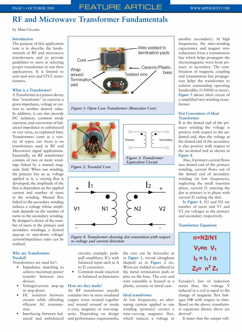
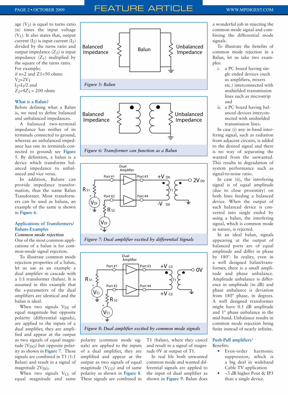
How are they made?An RF transformer usually contains two or more insulated copper wires twisted together and wound around or inside a core, magnetic or non-mag-netic. Depending on design and performance requirements,
the core can be binocular as in Figure 1, toroid (doughnut shaped) as in Figure 2 etc. Wires are welded or soldered to the metal termination pads or pins on the base. The core and wire ensemble is housed in a plastic, ceramic or metal case.
Ideal transformer At low frequencies, an alter-nating current applied to one winding (primary) creates a time-varying magnetic flux, which induces a voltage in
another (secondary). At high frequencies, the inter-winding capacitance and magnet wire inductance form a transmission line which helps propagate the electromagnetic wave from pri-mary to secondary. The com-bination of magnetic coupling and transmission line propaga-tion helps the transformer to achieve outstanding operating bandwidths (1:10000 or more). Figure 3 shows ideal circuit of a simplified two-winding trans-former.
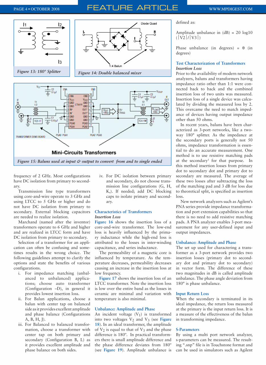
Dot Convention of Ideal TransformerIf at the dotted end of the pri-mary winding the voltage is positive with respect to the un-dotted end, then the voltage at the dotted end of the secondary is also positive with respect to the un-dotted end as shown in Figure 4.
Also, if primary current flows into dotted end of the primary winding, current flows out of the dotted end of secondary winding (at low frequencies, neglecting the small insertion phase, current I1 entering the dot at primary is in phase with current I2 exiting the dot).
In Figure 4, N1 and N2 are number of turns and V1 and V2 are voltages at the primary and secondary respectively.
Transformer Equations
Faraday’s law of induction states that, the voltage V induced in a coil is equal to the change of magnetic flux link-ages NΦ with respect to time. Based on the above, transform-er equations shown above are derived2.
It states that the output volt-
RF and Microwave Transformer Fundamentalsby Mini-Circuits
Figure 1: Open Case Transformer (Binocular Core)
V1
Fig 4
V2N1 N2
I1 I2 ++
- -Figure 4: Transformer showing dot convention with respect to voltage and current direction
Figure 2: Toroidal Core
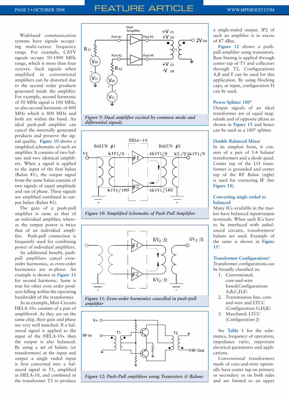
Primary Secondary
Fig 2Figure 3: Transformer Equivalent Circuit
PAGE 2 • OCTOBER 2009 www.mPdiGEsT.COmFEATURE ARTICLE
age (V2) is equal to turns ratio (n) times the input voltage (V1). It also states that, output current (I2) is input current (I1) divided by the turns ratio and output impedance (Z2) is input impedance (Z1) multiplied by the square of the turns ratio.For example; if n=2 and Z1=50 ohms:V2=2V1I2=I1/2 andZ2=4Z1 = 200 ohms
What is a Balun?Before defining what a Balun is, we need to define balanced and unbalanced impedances.
A balanced two-terminal impedance has neither of its terminals connected to ground, whereas an unbalanced imped-ance has one its terminals con-nected to ground; see Figure 5. By definition, a balun is a device which transforms bal-anced impedance to unbal-anced and vice versa.
In addition, Baluns can provide impedance transfor-mation, thus the name Balun Transformer. Most transform-ers can be used as baluns, an example of the same is shown in Figure 6.
Applications of Transformers/Baluns-ExamplesCommon mode rejectionOne of the most common appli-cations of a balun is for com-mon-mode signal rejection.
To illustrate common mode rejection properties of a balun, let us use as an example a dual amplifier in cascade with a 1:1 transformer (balun). It is assumed in this example that the s-parameters of the dual amplifiers are identical and the balun is ideal.
When two signals VDI of equal magnitude but opposite polarity (differential signals), are applied to the inputs of a dual amplifier, they are ampli-fied and appear at the output as two signals of equal magni-tude (VDO) but opposite polar-ity as shown in Figure 7. These signals are combined in T1 (1:1 Balun) and result in a signal of magnitude 2VDO.
When two signals VCI of equal magnitude and same
polarity (common mode sig-nals) are applied to the inputs of a dual amplifier, they are amplified and appear at the output as two signals of equal magnitude (VCO) and of same polarity as shown in Figure 8. These signals are combined in
T1 (balun), where they cancel and result in a signal of magni-tude 0V at output of T1.
In real life both unwanted common mode and wanted dif-ferential signals are applied to the input of dual amplifier as shown in Figure 9. Balun does
a wonderful job in rejecting the common mode signal and com-bining the differential mode signals.
To illustrate the benefits of common mode rejection in a Balun, let us take two exam-ples:
a PC board having sin-i. gle ended devices (such as amplifiers, mixers etc.) interconnected with unshielded transmission lines such as microstrip anda PC board having bal-ii. anced devices intercon-nected with unshielded transmission lines.
In case (i) any in-band inter-fering signal, such as radiation from adjacent circuits, is added to the desired signal and there is no way of separating the wanted from the unwanted. This results in degradation of system performance such as signal-to-noise ratio.
In case (ii), the interfering signal is of equal amplitude (due to close proximity) on both lines feeding a balanced device. When the output of such balanced device is con-verted into single ended by using a balun, the interfering signal, which is common mode in nature, is rejected.
In an ideal balun, signals appearing at the output of balanced ports are of equal amplitude and differ in phase by 180º. In reality, even in a well designed balun/trans-former, there is a small ampli-tude and phase unbalance. Amplitude unbalance is differ-ence in amplitude (in dB) and phase unbalance is deviation from 180º phase, in degrees. A well designed transformer might have 0.1 dB amplitude and 1º phase unbalance in the mid-band. Unbalance results in common mode rejection being finite instead of nearly infinite.
Push-Pull amplifiers3
Benefits:Even-order harmonic •suppression, which is a big deal in wideband Cable TV application~3 dB higher Pout & IP3 •than a single device.
Fig 5
UnbalancedImpedanceImpedance
Balanced Balun
Figure 5: Balun
ImpedanceBalanced
ImpedanceUnbalanced
Fig 6Figure 6: Transformer can function as a Balun
T1
Ampli�erDual
Port #3
Port #4
Port #1
Port #2
+V D02V D0
-V D0
R S2
R S1
VDI
VDI
-
+
Fig 7
+
-
Figure 7: Dual amplifier excited by differential Signals
Fig 8
-
+R S1
+V C0
T1
VCI
R S2
Port #2 Port #4
+V C0
Ampli�er
Port #1
Dual
Port #30V
VCI
-
+
Figure 8: Dual amplifier excited by common mode signals
PAGE 3 • OCTOBER 2008 www.mPdiGEsT.COmFEATURE ARTICLE
Wideband communication systems have signals occupy-ing multi-octave frequency range. For example, CATV signals occupy 50-1000 MHz range, which is more than four octaves. Such signals when amplified in conventional amplifiers can be distorted due to the second order products generated inside the amplifier. For example, second harmonic of 50 MHz signal is 100 MHz, so also second harmonic of 400 MHz which is 800 MHz and both are within the band. An ideal push-pull amplifier can cancel the internally generated products and preserve the sig-nal quality. Figure 10 shows a simplified schematic of such an amplifier. It consists of two bal-uns and two identical amplifi-ers. When a signal is applied to the input of the first balun (Balun #1), the output signal from the same balun consists of two signals of equal amplitude and out of phase. These signals are amplified combined in out-put balun (Balun #2).
The gain of a push-pull amplifier is same as that of an individual amplifier, where-as the output power is twice that of an individual ampli-fier. Push-pull connection is frequently used for combining power of individual amplifiers.
An additional benefit, push-pull amplifiers cancel even-order harmonics, as even-order harmonics are in-phase. An example is shown in Figure 11 for second harmonic. Same is true for other even order prod-ucts falling within the operating bandwidth of the transformer.
As an example, Mini-Circuits HELA-10+ consists of a pair of amplifiers4. As they are on the same chip, their gain and phase are very well matched. If a bal-anced signal is applied to the input of the HELA-10+ then the output is also balanced. By using a set of baluns (or transformers) at the input and output a single ended input is first converted into a bal-anced signal in T1, amplified in HELA-10, and combined in the transformer T2 to produce
a single-ended output. IP2 of such an amplifier is in excess of 87 dBm.
Figure 12 shows a push-pull amplifier using transistors. Base biasing is applied through center tap of T1 and collectors through T2. Configurations A,B and F can be used for this application. By using blocking caps, at input, configuration H can be used.
Power Splitter 180ºOutput signals of an ideal transformer are of equal mag-nitude and of opposite phase as shown in Figure 13 and hence can be used as a 180° splitter.
Double Balanced MixerIn its simplest form, it con-sists of a pair of 1:4 baluns/transformers and a diode quad. Center tap of the LO trans-former is grounded and center tap of the RF Balun (right) is used for extracting IF (See Figure 14).
Converting single ended to balancedMany ICs available in the mar-ket have balanced input/output terminals. When such ICs have to be interfaced with unbal-anced circuits, transformers/baluns are used. Example of the same is shown in Figure 155.
Transformer Configurations6
Transformer configurations can be broadly classified as:
Conventional; 1. core-and-wire based(Configurations A,B,C,D,F)Transmission line; core-2. and-wire and LTCC (Configuration G,H,K)Marchand; LTCC 3. (Configuration J)
See Table 1 for the sche-matics, frequency of operation, impedance ratio, important electrical parameters and appli-cations.
Conventional transformers made of core-and-wire option-ally have center tap on primary or secondary or on both sides and are limited to an upper
Figure 11: Even-order harmonics cancelled in push-pull amplifier
Figure 10: Simplified Schematic of Push-Pull Amplifier
Fig 12
RF-Out
RF-In
V+
T1 T2
Figure 12: Push-Pull amplifiers using Transistors & Baluns
Fig 9
VDI
-
+R S1
-V D0
T1
VDI
R S2
Port #2 Port #4
+V D0
Ampli�er
Port #1
Dual
Port #32V D0
VCI
-
++
-
-VCI
+
+V C0
+V C0
Figure 9: Dual amplifier excited by common mode and differential signals
PAGE 4 • OCTOBER 2008 www.mPdiGEsT.COmFEATURE ARTICLE
frequency of 2 GHz. Most configurations have DC isolation from primary to second-ary.
Transmission line type transformers using core-and-wire operate to 3 GHz and using LTCC to 5 GHz or higher and do not have DC isolation from primary to secondary. External blocking capacitors are needed to realize isolation.
Marchand (named after the inventor) transformers operate to 6 GHz and higher and are realized in LTCC form and have DC isolation from primary to secondary.
Selection of a transformer for an appli-cation can often be confusing and some-times results in the wrong choice. The following guidelines attempt to clarify the options and state the benefits of various configurations.
For impedance matching (unbal-i. anced to unbalanced) applica-tions; choose auto transformer (Configuration –D), in general it provides lowest insertion loss.For Balun applications, choose a ii. balun with center tap on balanced side as it provides excellent amplitude and phase balance (Configurations A, B, H, J).For Balanced to balanced transfor-iii. mation, choose a transformer with center tap on both primary and secondary (Configuration B, L) as it provides excellent amplitude and phase balance on both sides.
For DC isolation between primary iv. and secondary, do not choose trans-mission line configurations (G, H, K,). If needed; add DC blocking caps to isolate primary and second-ary.
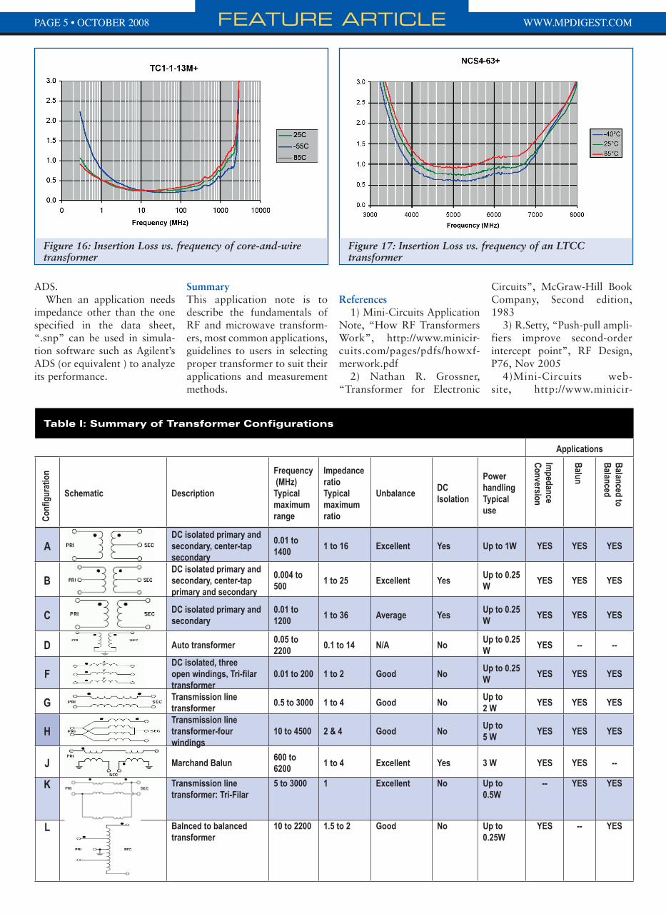
Characteristics of TransformersInsertion LossFigure 16 shows the insertion loss of a core-and-wire transformer. The low-end loss is heavily influenced by the prima-ry inductance while the high-end loss is attributed to the losses in inter-winding capacitance, and series inductance.
The permeability of a magnetic core is influenced by temperature. As the tem-perature decreases, permeability decreases causing an increase in the insertion loss at low frequency.
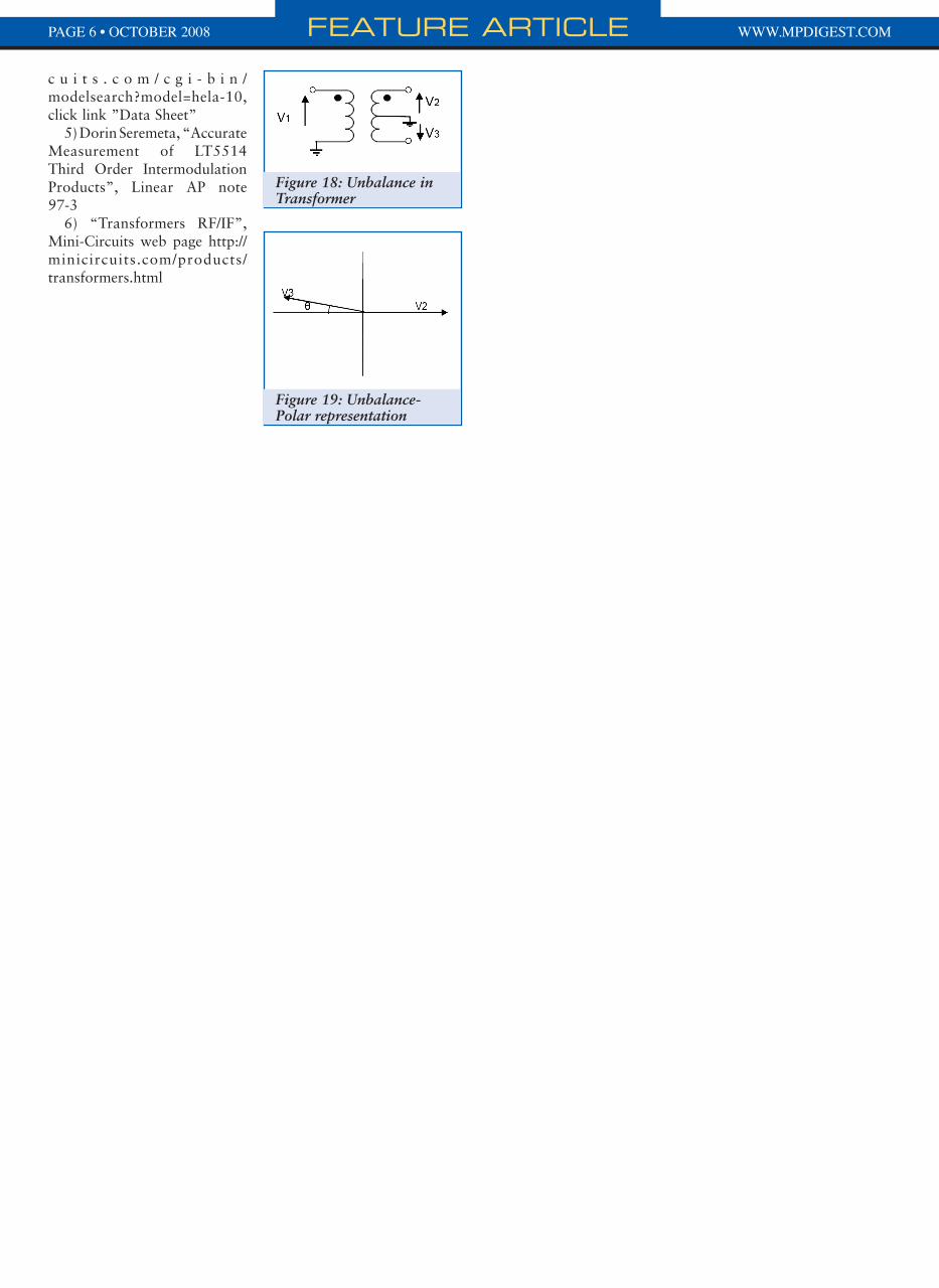
Figure 17 shows the insertion loss of an LTCC transformer. Note the insertion loss is low over the entire band as the losses in ceramic are minimal and variation with temperature is also minimal.
Unbalance: Amplitude and PhaseAn incident voltage (V1) is transformed into two voltages V2 and V3 (see Figure 18). In an ideal transformer, the amplitude of V2 is equal to that of V3 and the phase difference is 180º. In practical transform-ers there is small amplitude difference and the phase difference deviates from 180º (see Figure 19). Amplitude unbalance is
defined as:
Amplitude unbalance in (dB) = 20 log10 (V2/V3)
Phase unbalance (in degrees) = θ (in degrees)
Test Characterization of TransformersInsertion LossPrior to the availability of modern network analyzers, baluns and transformers having impedance ratio other than 1:1 were con-nected back to back and the combined insertion loss of two units was measured. Insertion loss of a single device was calcu-lated by dividing the measured loss by 2. This overcame the need to match imped-ance of devices having output impedance other than 50 ohms.
In recent years, baluns have been char-acterized as 3-port networks, like a two-way 180° splitter. As the impedance at the secondary ports is generally not 50 ohms, impedance transformation is essen-tial to do an accurate measurement. One method is to use resistive matching pads at the secondary1 for that purpose. In this method insertion losses from primary dot to secondary dot and primary dot to secondary are measured. The average of these two losses after subtracting the loss of the matching pad and 3 dB for loss due to theoretical split, is specified as insertion loss.
New network analyzers such as Agilent’s PNA series provide impedance transforma-tion and port extension capabilities so that there is no need to add resistive matching pads. A PNA analyzer enables 3-port mea-surement for any user-defined input and output impedances.
Unbalance: Amplitude and PhaseThe set up used for charactering a trans-former as a 3-port network provides two insertion losses (primary dot to second-ary dot and primary dot to secondary) in vector form. The difference of these two magnitudes in dB is called amplitude unbalance. The phase angle deviation from 180° is phase unbalance.
Input Return LossWhen the secondary is terminated in its ideal impedance, the return loss measured at the primary is the input return loss. It is a measure of the effectiveness of the balun in transforming impedance.
S-ParametersBy using a multi port network analyzer, s-parameters can be measured. The result-ing “.snp” file is in Touchstone format and can be used in simulators such as Agilent
Figure 13: 180° Splitter Figure 14: Double balanced mixer
Figure 15: Baluns used at input & output to convert from and to single ended
PAGE 5 • OCTOBER 2008 www.mPdiGEsT.COmFEATURE ARTICLE
Table I: Summary of Transformer Configurations
Applications
Con
figur
atio
n
Schematic Description
Frequency (MHz)Typical maximum range
Impedance ratioTypical maximum ratio
UnbalanceDCIsolation
Power handlingTypical use
Impedance
Conversion
Balun
Balanced to
Balanced
ADC isolated primary and secondary, center-tap secondary
0.01 to 1400
1 to 16 Excellent Yes Up to 1W YES YES YES
BDC isolated primary and secondary, center-tap primary and secondary
0.004 to 500
1 to 25 Excellent YesUp to 0.25 W
YES YES YES
CDC isolated primary and secondary
0.01 to 1200
1 to 36 Average YesUp to 0.25 W
YES YES YES
D Auto transformer0.05 to 2200
0.1 to 14 N/A NoUp to 0.25 W
YES -- --
FDC isolated, three open windings, Tri-filar transformer
0.01 to 200 1 to 2 Good NoUp to 0.25 W
YES YES YES
GTransmission line transformer
0.5 to 3000 1 to 4 Good NoUp to 2 W
YES YES YES
HTransmission line transformer-four windings
10 to 4500 2 & 4 Good NoUp to 5 W
YES YES YES
J Marchand Balun600 to 6200
1 to 4 Excellent Yes 3 W YES YES --
K Transmission line transformer: Tri-Filar
5 to 3000 1 Excellent No Up to 0.5W
-- YES YES
L Balnced to balanced transformer
10 to 2200 1.5 to 2 Good No Up to 0.25W
YES -- YES
ADS. When an application needs
impedance other than the one specified in the data sheet, “.snp” can be used in simula-tion software such as Agilent’s ADS (or equivalent ) to analyze its performance.
SummaryThis application note is to describe the fundamentals of RF and microwave transform-ers, most common applications, guidelines to users in selecting proper transformer to suit their applications and measurement methods.
References1) Mini-Circuits Application
Note, “How RF Transformers Work”, http://www.minicir-cuits.com/pages/pdfs/howxf-merwork.pdf
2) Nathan R. Grossner, “Transformer for Electronic
Circuits”, McGraw-Hill Book Company, Second edition, 1983
3) R.Setty, “Push-pull ampli-fiers improve second-order intercept point”, RF Design, P76, Nov 2005
4)Mini-Circuits web-site, http://www.minicir-
Figure 16: Insertion Loss vs. frequency of core-and-wire transformer
Figure 17: Insertion Loss vs. frequency of an LTCC transformer
PAGE 6 • OCTOBER 2008 www.mPdiGEsT.COmFEATURE ARTICLE
c u i t s . c o m / c g i - b i n /modelsearch?model=hela-10, click link ”Data Sheet”
5) Dorin Seremeta, “Accurate Measurement of LT5514 Third Order Intermodulation Products”, Linear AP note 97-3
6) “Transformers RF/IF”, Mini-Circuits web page http://minicircuits.com/products/transformers.html
Figure 18: Unbalance in Transformer
Figure 19: Unbalance-Polar representation


![Modeling of Integrated Octagonal Planar Transformer for RF …article.ijimse.org/pdf/10.11648.j.ijimse.20190406.11.pdf · electric diagram presented by [10], which shows the π model](https://img.pdfslide.net/doc/110x75/5fd8fdf5ebec50619b05dc81/modeling-of-integrated-octagonal-planar-transformer-for-rf-electric-diagram-presented.jpg)