Embed Size (px)
Citation preview
PAM4 digital receiver performance and feasibilityp y
Vasu ParthasarathyJan 2012Jan 2012
www.broadcom.com
Supporters and Contributors
• Howard Frazier, Broadcom• Will Bliss, Broadcom• Kent Lusted, Intel• Rich Mellitz Intel• Rich Mellitz, Intel• Sanjay Kasturia, Inphi• Hamid Rategh, Inphi• Adee Ran, Intel• Matt Brown, Applied Micro
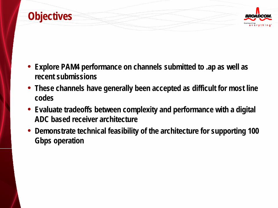
Objectives
• Explore PAM4 performance on channels submitted to .ap as well as recent submissions
• These channels have generally been accepted as difficult for most line These channels have generally been accepted as difficult for most line codes
• Evaluate tradeoffs between complexity and performance with a digital ADC based receiver architectureADC based receiver architecture
• Demonstrate technical feasibility of the architecture for supporting 100 Gbps operation
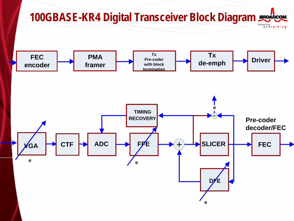
100GBASE-KR4 Digital Transceiver Block Diagram
Txde emph Driver
TxPre-coder
ith bl kPMA
fFEC
d de-emphwith block termination
framerencoder
TIMING RECOVERY -
e
Pre-coder d d /FEC
VGA ADC FFE SLICER+ FECCTF
decoder/FEC
DFE
e e
e
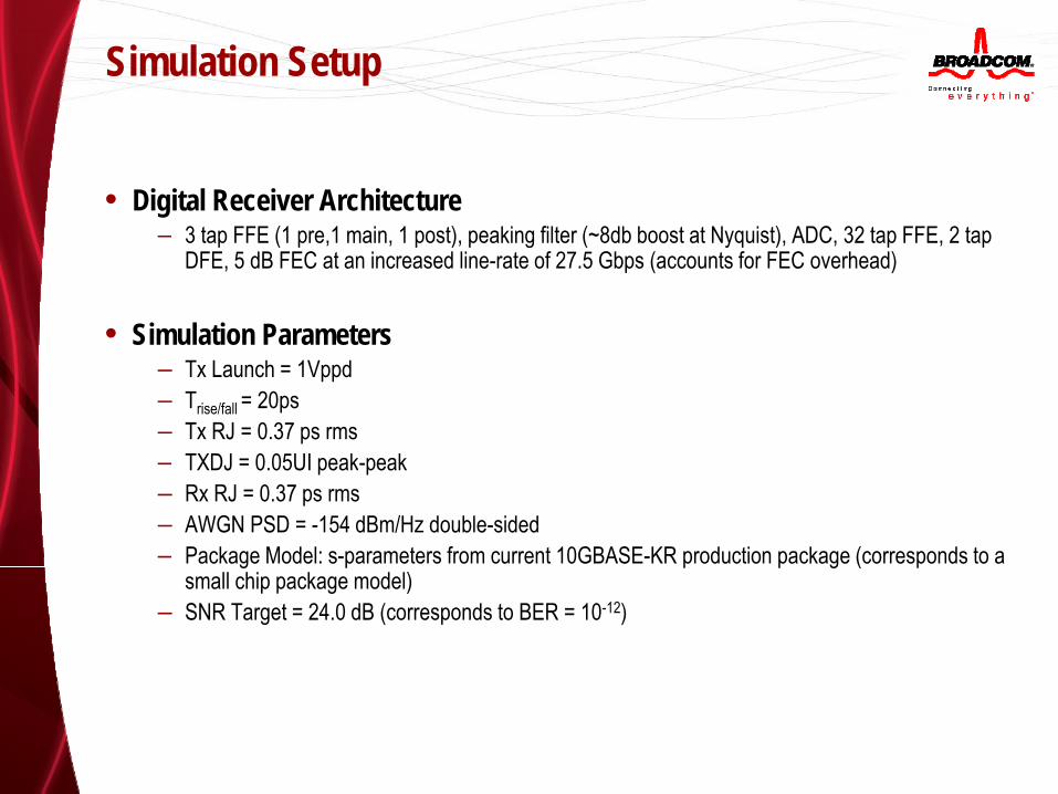
Simulation Setup
• Digital Receiver Architecture3 t FFE (1 1 i 1 t) ki filt ( 8db b t t N i t) ADC 32 t FFE 2 t – 3 tap FFE (1 pre,1 main, 1 post), peaking filter (~8db boost at Nyquist), ADC, 32 tap FFE, 2 tap DFE, 5 dB FEC at an increased line-rate of 27.5 Gbps (accounts for FEC overhead)
• Simulation ParametersSimulation Parameters– Tx Launch = 1Vppd– Trise/fall = 20ps– Tx RJ = 0.37 ps rms
TXDJ 0 0 UI k k– TXDJ = 0.05UI peak-peak– Rx RJ = 0.37 ps rms– AWGN PSD = -154 dBm/Hz double-sided– Package Model: s-parameters from current 10GBASE-KR production package (corresponds to a g p p p g ( p
small chip package model)– SNR Target = 24.0 dB (corresponds to BER = 10-12)
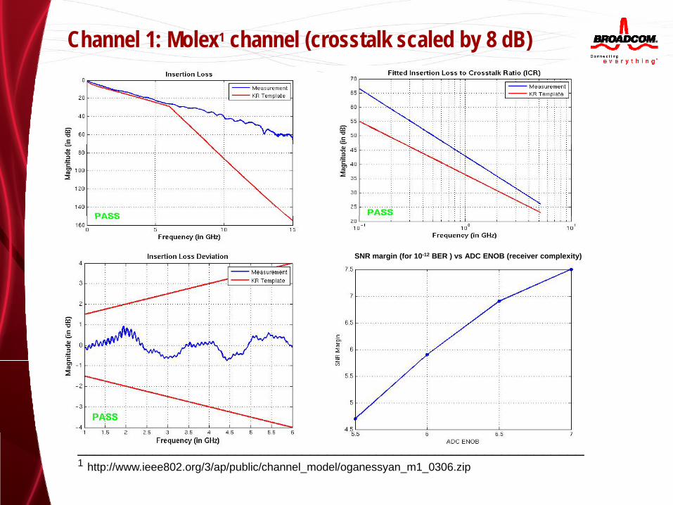
Channel 1: Molex1 channel (crosstalk scaled by 8 dB)
SNR margin (for 10-12 BER ) vs ADC ENOB (receiver complexity)
_____________________________________________________________1 http://www.ieee802.org/3/ap/public/channel_model/oganessyan_m1_0306.zip
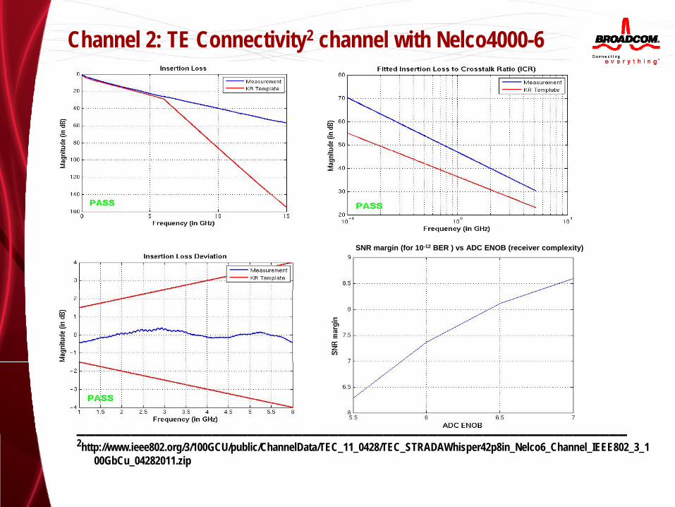
Channel 2: TE Connectivity2 channel with Nelco4000-6
SNR margin (for 10-12 BER ) vs ADC ENOB (receiver complexity)
__________________________________________________________________________________________________________________________2http://www.ieee802.org/3/100GCU/public/ChannelData/TEC_11_0428/TEC_STRADAWhisper42p8in_Nelco6_Channel_IEEE802_3_1
00GbCu_04282011.zip
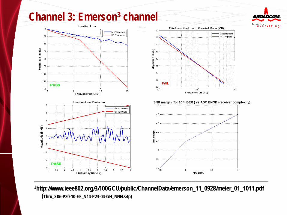
Channel 3: Emerson3 channel
SNR margin (for 10-12 BER ) vs ADC ENOB (receiver complexity)
_____________________________________________________________3http://www.ieee802.org/3/100GCU/public/ChannelData/emerson_11_0928/meier_01_1011.pdf
(Thru_S06-P20-10-EF_S14-P23-04-GH_NNN.s4p)
Transmitter Feasibility
• Transmitters have been built with 10 taps of de-emphasis for NRZ designs at 10 Gbps4
Lit t t f 5 t d h i PAM4 t itt t 20 Gb 5 6• Literature reports of an 5 tap de-emphasis PAM4 transmitter at 20 Gbps5,6
• High precision DAC’s have been fabricated around rates of 24 Gbps (12 Gsamples/sec)7
• PAM4 transmitter with 3 tap de emphasis should be feasible in current technology • PAM4 transmitter with 3 tap de-emphasis should be feasible in current technology at a reasonable power
______________________________________________________________4 D.Crivelli et. al., “Architecture and Experimental Evaluation of a 10Gb/s MLSD based Transceiver for Optical Multimode applications”,
Proceedings of ICC, May 20085 Z.Gao et. al., “A 10 Gb/s Wire-line Transceiver with Half Rate Period Calibration CDR”, Proceedings of IEEE ISCAS, May 20096 A.Amirkhany et. al., “A 24 Gb/s Software Programmable Analog Multi-Tone Transmitter”, IEEE Journal of solid state circuits, April 20087 Greshishchev, Y.M. et. al., “A 56GS/S 6b DAC in 65nm CMOS with 256×6b memory”, Proceedings of the IEEE ISSCC, April 2011
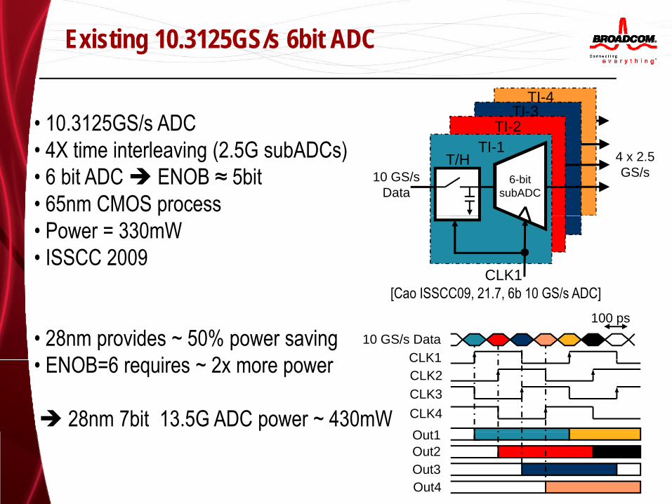
Existing 10.3125GS/s 6bit ADC
TI-4TI-3• 10.3125GS/s ADC
4X ti i t l i (2 5G bADC )TI-2
TI 14 x 2.5 GS/s10 GS/s
Data
• 4X time interleaving (2.5G subADCs)• 6 bit ADC ENOB ≈ 5bit• 65nm CMOS process
TI-1T/H
6-bitsubADC
CLK1[C ISSCC09 21 7 6b 10 GS/ ADC]
• Power = 330mW• ISSCC 2009
10 GS/s Data100 ps
CLK1
[Cao ISSCC09, 21.7, 6b 10 GS/s ADC]
• 28nm provides ~ 50% power savingENOB 6 i 2 CLK1
CLK2CLK3CLK4O t1
• ENOB=6 requires ~ 2x more power
28nm 7bit 13.5G ADC power ~ 430mWOut1Out2Out3Out4
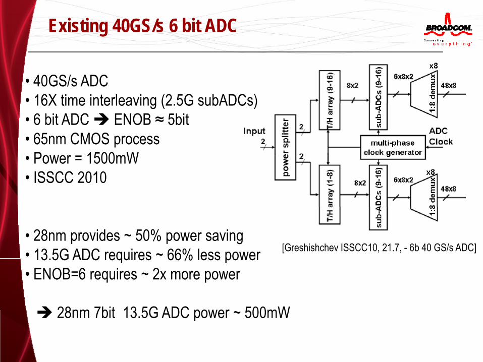
Existing 40GS/s 6 bit ADC
• 40GS/s ADC• 16X time interleaving (2 5G subADCs)16X time interleaving (2.5G subADCs)• 6 bit ADC ENOB ≈ 5bit• 65nm CMOS process
Po er 1500mW• Power = 1500mW• ISSCC 2010
• 28nm provides ~ 50% power saving• 13 5G ADC requires ~ 66% less power [Greshishchev ISSCC10, 21.7, - 6b 40 GS/s ADC]13.5G ADC requires 66% less power• ENOB=6 requires ~ 2x more power
28nm 7bit 13 5G ADC power 500mW 28nm 7bit 13.5G ADC power ~ 500mW
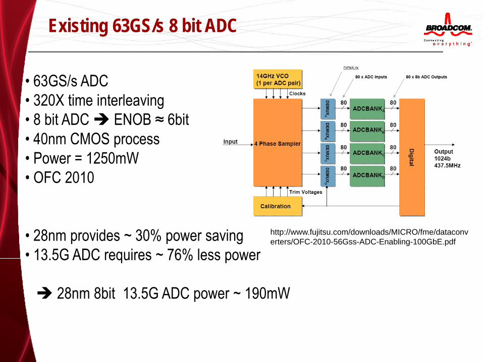
Existing 63GS/s 8 bit ADC
• 63GS/s ADC• 320X time interleaving320X time interleaving• 8 bit ADC ENOB ≈ 6bit• 40nm CMOS process
Po er 1250mW• Power = 1250mW• OFC 2010
• 28nm provides ~ 30% power saving• 13 5G ADC requires ~ 76% less power
http://www.fujitsu.com/downloads/MICRO/fme/dataconverters/OFC-2010-56Gss-ADC-Enabling-100GbE.pdf
13.5G ADC requires 76% less power
28nm 8bit 13.5G ADC power ~ 190mW
ADC Feasibility …..
• 10-50G ADCs with 5-6 bit ENOB have been successfully implemented as well as presented in major conferences
• 7bit 13.5G ADC power can be in 190-500mW range depending on the architectural and circuit implementation
• Further improvements in ADC is possible with architectural considerations tailored towards the PAM4 situation
Equalizer (FFE) Feasibility
• Synthesized a parallelized 32 tap FFE with 40nm std cell TSMC library (effective bit-rate is around 26 Gbps)
• Develops on a Fast FFE implementation8
• Production part type synthesis with 20% timing margin to worst PVT corner (to estimate feasibility, area and power)co e (to est ate eas b ty, a ea a d po e )
• Straightforward Fast FFE implementation, further optimizations possible in tap widths and adders for smaller area, power and latency
• POWER (Synopsys DC estimated pre layout static + dynamic): around • POWER (Synopsys DC estimated pre-layout, static + dynamic): around twice that of a 10 tap KR FFE implementation at 10.5 Gbps
• Process node change to 28nm/20nm would further reduce the FFE b t l t 30%power by at least 30%
______________________________________________________________8 Richard Blahut, “Fast Algorithms for Digital Signal Processing”, Addison-Wesley, 1985
Equalizer (DFE) Feasibility• Synthesized a 2 tap look-ahead9 PAM4 DFE with 40nm std cell library
(effective bit-rate is around 26 Gbps)• Production part type synthesis with 20% timing margin to worst PVT Production part type synthesis with 20% timing margin to worst PVT
corner (to estimate feasibility, area and power)• Straightforward implementation used, further optimizations possible in
look-ahead structure for lower area/power/latencylook-ahead structure for lower area/power/latency• Note that some amount of duty-cycle distortion (DCD) can be cancelled
with a look-ahead DFE architecturePOWER (S DC ti t d l t t ti d i ) i il • POWER (Synopsys DC estimated pre-layout, static + dynamic) : similar to a 4 tap NRZ DFE at KR rates of 10.5 Gbps
• Process node change to 28nm/20nm would further reduce the FFE power by at least 30%
_____________________________________________________________9 Keshab K. Parhi, “Design of Multigigabit Multiplexer-Loop-Based Decision Feedback Equalizers”, IEEE Transactions
O V L S l I t ti (VLSI) t V l 13 N 4 A il 2005On Very Large Scale Integration (VLSI) systems, Vol. 13, No.4, April 2005
Other blocks …
• PGA adaptation blocks typically run at low speed (highly sub-sampled line-rate clock)
• LMS adaptation for stationary channels also typically run at very low speeds
• Timing recovery algorithms10 for PAM4 are relatively simple to g y g y pimplement
• FEC block codes which provide 5 dB coding gain are readily available and have been presented at IEEE11, 12and have been presented at IEEE
• These codes have been analyzed in detail and shown to be low in power and area irrespective of the choice of line code
________________________________________________________________10 K. H. Mueller and M. S. Muller, “Timing Recovery in Digital Synchronous Data Receivers”, IEEETransactions on Communications, vol. COM-24, pp. 516-531, May 197611 S.Bhoja et. al., “Precoding proposal for PAM4 modulation”, IEEE Chicago meeting, Sept. 2011 j g p p g g p12 Z.Wang and C.J.Chen, “ Feasibility of 100G-KR FEC”, IEEE Lake Tahoe meeting, May 2011
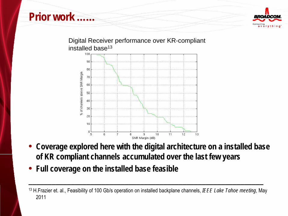
Prior work ……
Digital Receiver performance over KR-compliant installed base13
• Coverage explored here with the digital architecture on a installed base f KR li t h l l t d th l t f of KR compliant channels accumulated over the last few years
• Full coverage on the installed base feasible_____________________________________________________________13 H.Frazier et. al., Feasibility of 100 Gb/s operation on installed backplane channels, IEEE Lake Tahoe meeting, May
2011
Conclusions
• Demonstrated that it is technically feasible to by use PAM4 as the line d / d l ti t h icode/modulation technique
• Examined the performance of a digital PAM4 receiver architectures over p gsome channels submitted to IEEE
• All of the major blocks required for an implementation are technically • All of the major blocks required for an implementation are technically and economically feasible using current technology