Embed Size (px)
Citation preview
Parasitic Oscillation and Ringing of Power MOSFETs Application Note
2018-07-26 1 © 2017 - 2018 Toshiba Electronic Devices & Storage Corporation
Description This document describes the causes of and solutions for parasitic oscillation and ringing of power MOSFETs.
Parasitic Oscillation and Ringing of Power MOSFETs
Parasitic Oscillation and Ringing of Power MOSFETs Application Note
2018-07-26 2 © 2017 - 2018 Toshiba Electronic Devices & Storage Corporation
Table of Contents Description ............................................................................................................................................ 1
Table of Contents ................................................................................................................................. 2
1. Parasitic oscillation and ringing of a standalone MOSFET .......................................................... 3
2. Forming of an oscillation network ....................................................................................................... 3
2.1. Oscillation phenomenon ..................................................................................................................... 3
2.1.1. Feedback circuit (positive and negative feedback) ......................................................................... 4
2.1.2. Conditions for oscillation ...................................................................................................................... 5
2.2. MOSFET oscillation .............................................................................................................................. 5
2.2.1. MOSFET feedback loop ........................................................................................................................ 5
2.2.2. Colpitts oscillators ................................................................................................................................. 6
2.2.3. Hartley oscillators ................................................................................................................................. 7
2.3. Parasitic oscillation of MOSFETs for switching applications (standalone MOSFET operation) 7
2.3.1. Parasitic oscillation circuits (parasitic oscillation loops) .................................................................. 8
2.3.2. Condition for parasitic oscillation .....................................................................................................10
2.4. Mitigating parasitic oscillation ...........................................................................................................11
3. Voltage ringing induced by the drain inductance ...................................................................... 12
3.1. Mechanism .......................................................................................................................................... 12
3.2. Mitigating the ringing ........................................................................................................................ 13
4. Voltage induced by the source lead and wire stray inductances ............................................. 14
4.1. Mitigating the ringing ........................................................................................................................ 14
5. Simulating and reducing oscillation and ringing of a MOSFET ................................................. 15
5.1. Oscillator ............................................................................................................................................. 15
5.1.1. Oscillation phenomenon ....................................................................................................................15
5.1.2. Mitigating oscillation ...........................................................................................................................16
5.2. Ringing caused by drain stray inductance ..................................................................................... 17
5.2.1. Ringing simulation ..............................................................................................................................17
5.2.2. Mitigating the ringing .........................................................................................................................18
5.3. Ringing caused by the source lead and wire stray inductances ................................................ 19
5.3.1. Ringing simulation ..............................................................................................................................19
5.3.2. Mitigating the ringing .........................................................................................................................20
RESTRICTIONS ON PRODUCT USE.................................................................................................. 21
Parasitic Oscillation and Ringing of Power MOSFETs Application Note
2018-07-26 3 © 2017 - 2018 Toshiba Electronic Devices & Storage Corporation
1. Parasitic oscillation and ringing of a standalone MOSFET This section discusses parasitic oscillation and ringing of a MOSFET in switching applications. The oscillation and ringing of the gate voltage could cause false switching, increase power losses and lead to permanent damage of a MOSFET. Major causes of the oscillation and ringing of a MOSFET are as follows:
(1) Forming of an oscillation circuit An oscillation network is formed in a circuit and leads to parasitic oscillation of a MOSFET.
(2) Surge voltage across the drain and source The ringing voltage between the drain and the source during turn-off could return to the gate terminal through a positive feedback loop via the gate-drain capacitance Cgd and cause the gate voltage to oscillate.
(3) Source inductance A voltage induced by the di/dt of the drain-source current during turn-off and the source lead and wire stray inductances could cause the gate-source loop of a MOSFET to go into LCR resonance. (Ringing induced by the source inductance) Other factors could also cause oscillation and ringing, but stray inductance is of primary importance in using MOSFETs.
2. Forming of an oscillation network 2.1. Oscillation phenomenon Oscillation is a phenomenon whereby an electronic circuit causes voltage and current vibration on its own without receiving vibration energy from an external source. In reality, since a circuit has electric resistance, oscillations decay with time unless the lost energy is supplied to the circuit. The conditions for oscillation are: (1) Phase condition
The feedback signal from the output to the input is in phase with the input signal at the oscillation frequency. (Positive feedback loop) (2) Amplitude condition
The loss caused by passive elements in a circuit is lower than the gain obtained by an amplifier. Oscillation occurs when a circuit has a positive feedback and provides a gain that compensates for a loss.
Parasitic Oscillation and Ringing of Power MOSFETs Application Note
2018-07-26 4 © 2017 - 2018 Toshiba Electronic Devices & Storage Corporation
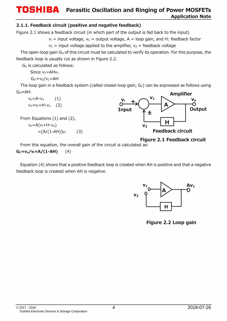
2.1.1. Feedback circuit (positive and negative feedback) Figure 2.1 shows a feedback circuit (in which part of the output is fed back to the input).
vi = input voltage, vo = output voltage, A = loop gain, and H: feedback factor v1 = input voltage applied to the amplifier, v2 = feedback voltage
The open-loop gain GO of this circuit must be calculated to verify its operation. For this purpose, the feedback loop is usually cut as shown in Figure 2.2.
Go is calculated as follows: Since v2=AHv1 GO=v2/v1=AH The loop gain in a feedback system (called closed-loop gain, GC) can be expressed as follows using
GO=AH: vo=A・v1 (1) v1=vi+H・vo (2)
From Equations (1) and (2), vo=A(vi+H・vo)
=[A/(1-AH)]vi (3)
From this equation, the overall gain of the circuit is calculated as: GC=vo/vi=A/(1-AH) (4)
Equation (4) shows that a positive feedback loop is created when AH is positive and that a negative feedback loop is created when AH is negative.
Amplifier
A
H ±
+ vi vo
Feedback circuit
Figure 2.1 Feedback circuit
v1
Input Output
v2
A
H
v1 Av1
v2
Figure 2.2 Loop gain
Parasitic Oscillation and Ringing of Power MOSFETs Application Note
2018-07-26 5 © 2017 - 2018 Toshiba Electronic Devices & Storage Corporation
2.1.2. Conditions for oscillation A positive feedback loop becomes unstable and oscillates when it has a gain AH of 1 or
greater. Therefore, a positive feedback loop is not generally used in amplifiers; it is commonly used in
oscillators (such as Wien bridge oscillators, Colpitts oscillators and Hartley oscillators). Here, let’s confine our discussion to positive feedback loops. Then, when AH=1 in Equation (4), GC becomes infinite, causing a feedback circuit to go into oscillation.
The loop gain AH of a positive feedback loop in an oscillator is expressed using a complex number. In a complex number a + bi, a is the real part and b is the imaginary part. Let the real part be Re(AH) and the imaginary part be Im(AH). Then, the conditions for oscillation are:
AH=Re(AH)+jIm(AH) Re(AH)≥1
2.2. MOSFET oscillation
Power MOSFETs have a large transconductance gm and parasitic capacitances. Therefore, wire and other stray inductances (inductances between the gate, source, and drain circuits and in the associated interconnects) could form a positive feedback circuit, causing parasitic oscillation.
The oscillating voltage could produce voltage overshoot on the positive feedback loop and the gate, leading to permanent damage of the MOSFET.
When a power MOSFET is in the steady on or off state, parasitic oscillation does not occur because its transconductance gm becomes zero or negligibly small. A power MOSFET is susceptible to parasitic oscillation: 1) when its load is short-circuited; and 2) during transient switching periods in which gm becomes large. Since the MOSFET is operating in linear mode (i.e., vDS and iD are being applied simultaneously), a positive feedback path can be formed by electromagnetic induction, parasitic capacitance and other factors. MOSFETs with a high gm go into parasitic oscillation when their loop gain is 1 or greater. 2.2.1. MOSFET feedback loop
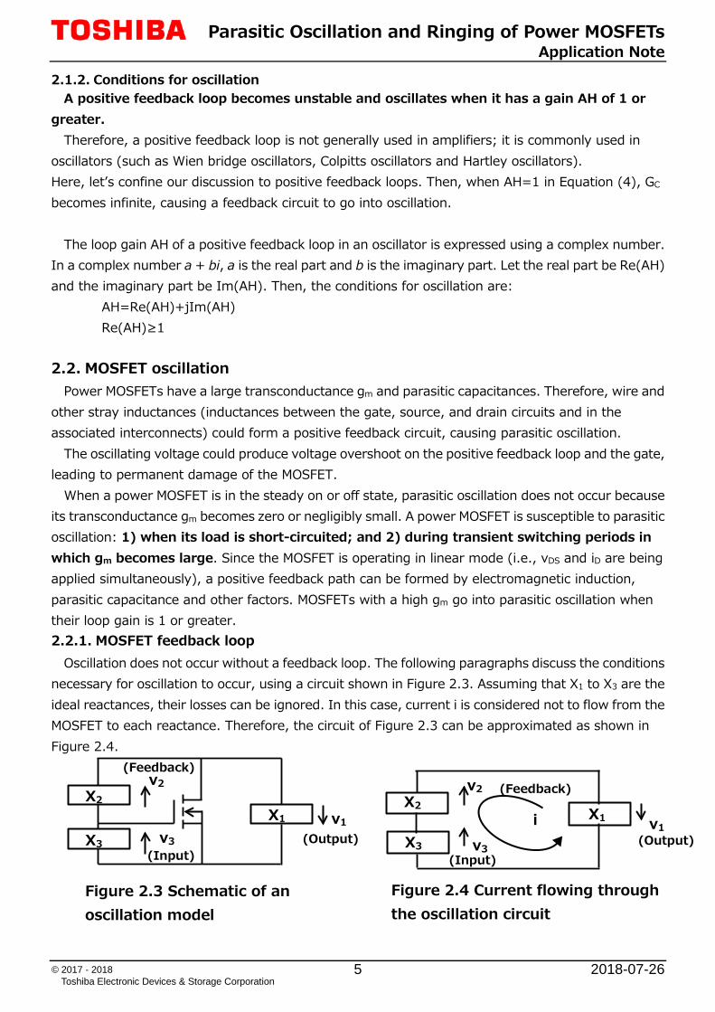
Oscillation does not occur without a feedback loop. The following paragraphs discuss the conditions necessary for oscillation to occur, using a circuit shown in Figure 2.3. Assuming that X1 to X3 are the ideal reactances, their losses can be ignored. In this case, current i is considered not to flow from the MOSFET to each reactance. Therefore, the circuit of Figure 2.3 can be approximated as shown in Figure 2.4.
v2 X2
X1
X3 v3
v1 i
v2 X2
X1
X3 v3
Figure 2.3 Schematic of an oscillation model
Figure 2.4 Current flowing through the oscillation circuit
v1
(Input)
(Output)
(Input)
(Output)
(Feedback)
(Feedback)
Parasitic Oscillation and Ringing of Power MOSFETs Application Note
2018-07-26 6 © 2017 - 2018 Toshiba Electronic Devices & Storage Corporation
v2 v1
×
C3
C1
L2
gm・v1
rd
+
-
According to Kirchhoff's circuit laws,
v1+v2+v3=i(X1+X2+X3)=0
Here, i≠0. Hence, X1+X2+X3=0
There is a positive feedback loop when the circuit is oscillating. This means that v3 (input) is in phase with v1 (output) in Figure 2.3 and Figure 2.4. Therefore, X3 and X1 are reactances of the same property; X2 is not.
Typical oscillators include Colpitts oscillators (Figure 2.5) and Hartley oscillators (Figure 2.6).
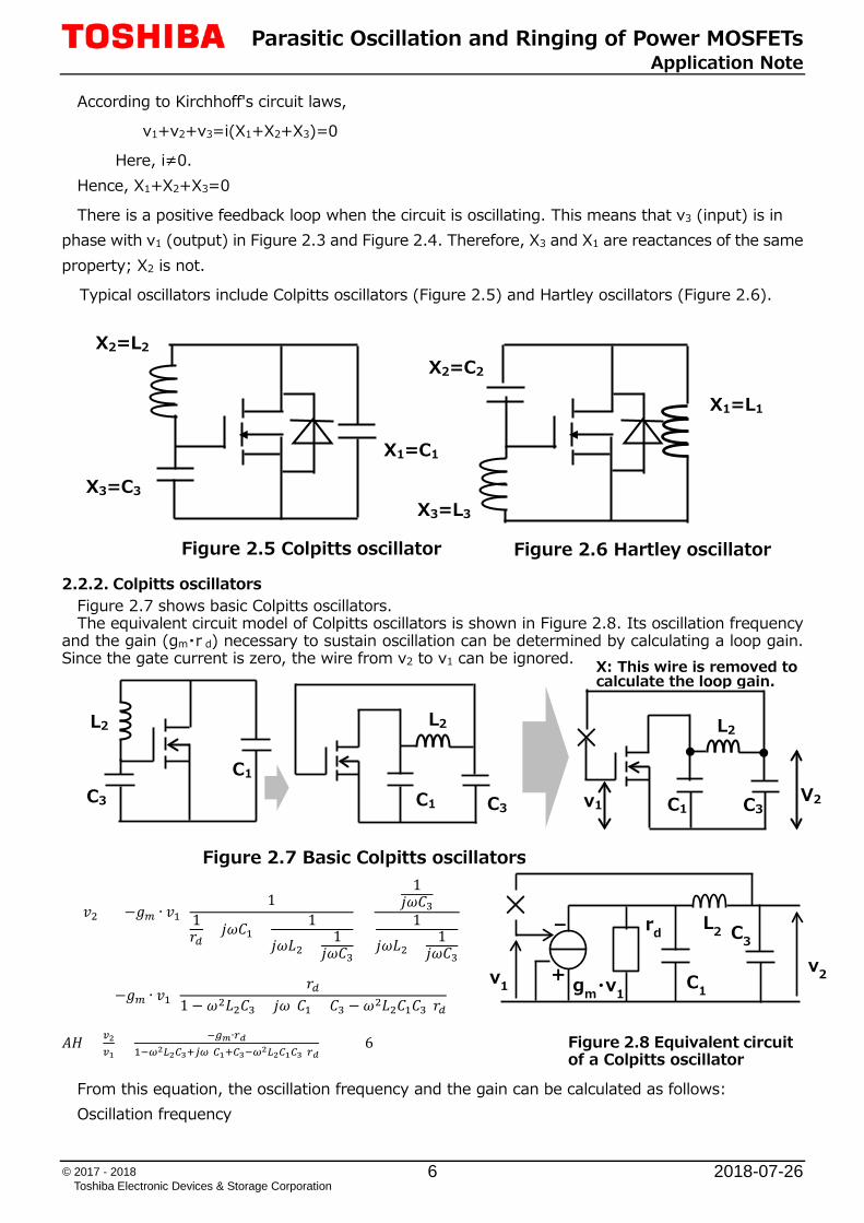
2.2.2. Colpitts oscillators
Figure 2.7 shows basic Colpitts oscillators. The equivalent circuit model of Colpitts oscillators is shown in Figure 2.8. Its oscillation frequency
and the gain (gm・r d) necessary to sustain oscillation can be determined by calculating a loop gain. Since the gate current is zero, the wire from v2 to v1 can be ignored.
𝑣𝑣2 = (−𝑔𝑔𝑚𝑚 ∙ 𝑣𝑣1)1
1𝑟𝑟𝑑𝑑
+ 𝑗𝑗𝑗𝑗𝐶𝐶1 + 1𝑗𝑗𝑗𝑗𝐿𝐿2 + 1
𝑗𝑗𝑗𝑗𝐶𝐶3
×
1𝑗𝑗𝑗𝑗𝐶𝐶3
1𝑗𝑗𝑗𝑗𝐿𝐿2 + 1
𝑗𝑗𝑗𝑗𝐶𝐶3
= (−𝑔𝑔𝑚𝑚 ∙ 𝑣𝑣1)
𝑟𝑟𝑑𝑑1 −𝑗𝑗2𝐿𝐿2𝐶𝐶3 + 𝑗𝑗𝑗𝑗(𝐶𝐶1 + 𝐶𝐶3 − 𝑗𝑗2𝐿𝐿2𝐶𝐶1𝐶𝐶3)𝑟𝑟𝑑𝑑
𝐴𝐴𝐴𝐴 = 𝑣𝑣2
𝑣𝑣1= −𝑔𝑔𝑚𝑚∙𝑟𝑟𝑑𝑑
1−𝜔𝜔2𝐿𝐿2𝐶𝐶3+𝑗𝑗𝜔𝜔(𝐶𝐶1+𝐶𝐶3−𝜔𝜔2𝐿𝐿2𝐶𝐶1𝐶𝐶3)𝑟𝑟𝑑𝑑 (6)
From this equation, the oscillation frequency and the gain can be calculated as follows: Oscillation frequency
X1=C1
X2=L2
Figure 2.5 Colpitts oscillator Figure 2.6 Hartley oscillator
X3=C3
X3=L3
X2=C2
X1=L1
X: This wire is removed to calculate the loop gain.
Figure 2.7 Basic Colpitts oscillators
V2
Figure 2.8 Equivalent circuit of a Colpitts oscillator
×
v1
L2
C3
C1
L2
C1 C3 C1 C3
L2
Parasitic Oscillation and Ringing of Power MOSFETs Application Note
2018-07-26 7 © 2017 - 2018 Toshiba Electronic Devices & Storage Corporation
Im(AH)=0 The Colpitts oscillator is most susceptible to oscillation at a frequency at which the phase of a signal
that has looped around the circuit once is delayed by 0° or 360°. Hence, C1 + 𝐶𝐶3 − 𝑗𝑗2𝐿𝐿2𝐶𝐶1𝐶𝐶3 = 0 (By dividing both sides of the equation by jωC1jωC3,
1/jωC1+1/jωC2+ jωL2=0 is obtained.)
𝑗𝑗2 =𝐶𝐶1 + 𝐶𝐶3𝐿𝐿2𝐶𝐶1𝐶𝐶3
(7) ω = �𝐶𝐶1 + 𝐶𝐶3𝐿𝐿2𝐶𝐶1𝐶𝐶3
(8)
Gain: Substituting Equation (7), ω2= (C1+C2) /L2C1C3, into Re(AH)≥1: −𝑔𝑔𝑚𝑚 ∙ 𝑟𝑟𝑑𝑑
1 − 𝐶𝐶1 + 𝐶𝐶3𝐿𝐿2𝐶𝐶1𝐶𝐶3
𝐿𝐿2𝐶𝐶3=𝑔𝑔𝑚𝑚 ∙ 𝑟𝑟𝑑𝑑𝐶𝐶3𝐶𝐶1
≥ 1 ∴ 𝑔𝑔𝑚𝑚 ∙ 𝑟𝑟𝑑𝑑 ≥𝐶𝐶3𝐶𝐶1
(9)
(gm・rd: Voltage loop gain) 2.2.3. Hartley oscillators
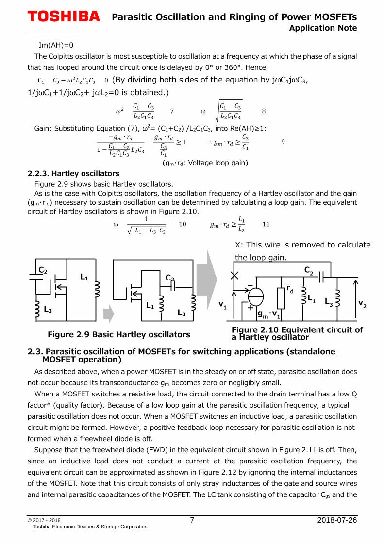
Figure 2.9 shows basic Hartley oscillators. As is the case with Colpitts oscillators, the oscillation frequency of a Hartley oscillator and the gain
(gm・r d) necessary to sustain oscillation can be determined by calculating a loop gain. The equivalent circuit of Hartley oscillators is shown in Figure 2.10.
ω =1
�(𝐿𝐿1 + 𝐿𝐿3)𝐶𝐶2 (10) 𝑔𝑔𝑚𝑚 ∙ 𝑟𝑟𝑑𝑑 ≥
𝐿𝐿1𝐿𝐿3
(11)
2.3. Parasitic oscillation of MOSFETs for switching applications (standalone
MOSFET operation) As described above, when a power MOSFET is in the steady on or off state, parasitic oscillation does
not occur because its transconductance gm becomes zero or negligibly small. When a MOSFET switches a resistive load, the circuit connected to the drain terminal has a low Q
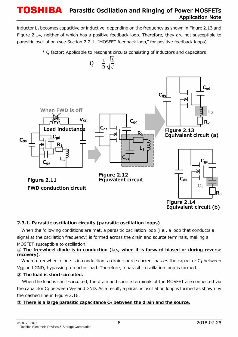
factor* (quality factor). Because of a low loop gain at the parasitic oscillation frequency, a typical parasitic oscillation does not occur. When a MOSFET switches an inductive load, a parasitic oscillation circuit might be formed. However, a positive feedback loop necessary for parasitic oscillation is not formed when a freewheel diode is off.
Suppose that the freewheel diode (FWD) in the equivalent circuit shown in Figure 2.11 is off. Then, since an inductive load does not conduct a current at the parasitic oscillation frequency, the equivalent circuit can be approximated as shown in Figure 2.12 by ignoring the internal inductances of the MOSFET. Note that this circuit consists of only stray inductances of the gate and source wires and internal parasitic capacitances of the MOSFET. The LC tank consisting of the capacitor Cgs and the
X: This wire is removed to calculate the loop gain.
L1 C2
L3 L1
L3
C2
Figure 2.9 Basic Hartley oscillators Figure 2.10 Equivalent circuit of a Hartley oscillator
×
L1 v1
rd
gm・v1
L3 v2
C2
+
-
Parasitic Oscillation and Ringing of Power MOSFETs Application Note
2018-07-26 8 © 2017 - 2018 Toshiba Electronic Devices & Storage Corporation
inductor L1 becomes capacitive or inductive, depending on the frequency as shown in Figure 2.13 and Figure 2.14, neither of which has a positive feedback loop. Therefore, they are not susceptible to parasitic oscillation (see Section 2.2.1, “MOSFET feedback loop,” for positive feedback loops). * Q factor: Applicable to resonant circuits consisting of inductors and capacitors
Q = 1R�𝐿𝐿𝐶𝐶
2.3.1. Parasitic oscillation circuits (parasitic oscillation loops)
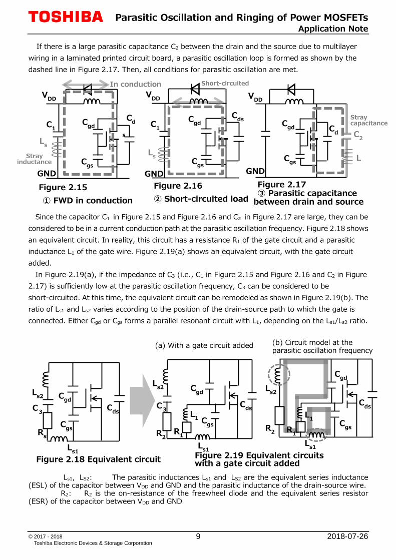
When the following conditions are met, a parasitic oscillation loop (i.e., a loop that conducts a signal at the oscillation frequency) is formed across the drain and source terminals, making a MOSFET susceptible to oscillation. ① The freewheel diode is in conduction (i.e., when it is forward biased or during reverse recovery).
When a freewheel diode is in conduction, a drain-source current passes the capacitor C1 between VDD and GND, bypassing a reactor load. Therefore, a parasitic oscillation loop is formed. ② The load is short-circuited. When the load is short-circuited, the drain and source terminals of the MOSFET are connected via the capacitor C1 between VDD and GND. As a result, a parasitic oscillation loop is formed as shown by the dashed line in Figure 2.16. ③ There is a large parasitic capacitance C2 between the drain and the source.
L2
R2
Figure 2.13 Equivalent circuit (a)
R3
Cgd
Cds
C1
Figure 2.14 Equivalent circuit (b)
Cds
Cgd
Cds Cgd
Cgs L1
R1
Load inductance
When FWD is off
Figure 2.11 FWD conduction circuit
VSP
Figure 2.12 Equivalent circuit
Cgd
Cds
Cgs
R1
L1
Parasitic Oscillation and Ringing of Power MOSFETs Application Note
2018-07-26 9 © 2017 - 2018 Toshiba Electronic Devices & Storage Corporation
If there is a large parasitic capacitance C2 between the drain and the source due to multilayer wiring in a laminated printed circuit board, a parasitic oscillation loop is formed as shown by the dashed line in Figure 2.17. Then, all conditions for parasitic oscillation are met.
Since the capacitor C1 in Figure 2.15 and Figure 2.16 and C2 in Figure 2.17 are large, they can be considered to be in a current conduction path at the parasitic oscillation frequency. Figure 2.18 shows an equivalent circuit. In reality, this circuit has a resistance R1 of the gate circuit and a parasitic inductance L1 of the gate wire. Figure 2.19(a) shows an equivalent circuit, with the gate circuit added.
In Figure 2.19(a), if the impedance of C3 (i.e., C1 in Figure 2.15 and Figure 2.16 and C2 in Figure 2.17) is sufficiently low at the parasitic oscillation frequency, C3 can be considered to be short-circuited. At this time, the equivalent circuit can be remodeled as shown in Figure 2.19(b). The ratio of Ls1 and Ls2 varies according to the position of the drain-source path to which the gate is connected. Either Cgd or Cgs forms a parallel resonant circuit with L1, depending on the Ls1/Ls2 ratio.
Ls1, LS2: The parasitic inductances Ls1 and LS2 are the equivalent series inductance (ESL) of the capacitor between VDD and GND and the parasitic inductance of the drain-source wire. R2: R2 is the on-resistance of the freewheel diode and the equivalent series resistor (ESR) of the capacitor between VDD and GND
Figure 2.18 Equivalent circuit Figure 2.19 Equivalent circuits with a gate circuit added
(a) With a gate circuit added (b) Circuit model at the parasitic oscillation frequency
Figure 2.15 ① FWD in conduction
Figure 2.16 ② Short-circuited load
Figure 2.17 ③ Parasitic capacitance
between drain and source
Stray inductance
Cgd
Cgs
In conduction
C1
Ls
Cd
s
GND
VDD Short-circuited
Ls
Cgd
Cgs
Cds
GND
VDD
C1 Cd C2
L
Stray capacitance Cgd
Cgs GND
VDD
Cgd
Cgs
Cds
Ls2
Ls1
Rs
C3
Cgd
Cgs
Cds
Ls2
Ls1
R2
C3 L1
R1
Cgd
Cgs
Cds
Ls2
Ls1
R2 R1
L1
Parasitic Oscillation and Ringing of Power MOSFETs Application Note
2018-07-26 10 © 2017 - 2018 Toshiba Electronic Devices & Storage Corporation
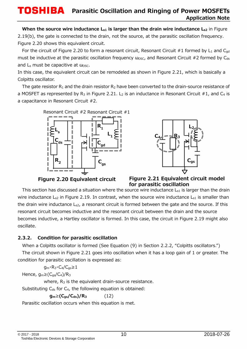
When the source wire inductance Ls1 is larger than the drain wire inductance Ls2 in Figure 2.19(b), the gate is connected to the drain, not the source, at the parasitic oscillation frequency. Figure 2.20 shows this equivalent circuit.
For the circuit of Figure 2.20 to form a resonant circuit, Resonant Circuit #1 formed by L1 and Cgd must be inductive at the parasitic oscillation frequency ωOSC, and Resonant Circuit #2 formed by Cds and Ls must be capacitive at ωOSC. In this case, the equivalent circuit can be remodeled as shown in Figure 2.21, which is basically a Colpitts oscillator.
The gate resistor R1 and the drain resistor R2 have been converted to the drain-source resistance of a MOSFET as represented by R3 in Figure 2.21. L2 is an inductance in Resonant Circuit #1, and C4 is a capacitance in Resonant Circuit #2.
This section has discussed a situation where the source wire inductance Ls1 is larger than the drain wire inductance Ls2 in Figure 2.19. In contrast, when the source wire inductance Ls1 is smaller than the drain wire inductance Ls2, a resonant circuit is formed between the gate and the source. If this resonant circuit becomes inductive and the resonant circuit between the drain and the source becomes inductive, a Hartley oscillator is formed. In this case, the circuit in Figure 2.19 might also oscillate. 2.3.2. Condition for parasitic oscillation
When a Colpitts oscillator is formed (See Equation (9) in Section 2.2.2, “Colpitts oscillators.”) The circuit shown in Figure 2.21 goes into oscillation when it has a loop gain of 1 or greater. The
condition for parasitic oscillation is expressed as: gm・R3・C4/Cgs≥1
Hence, gm≥(Cgs/C4)/R3 where, R3 is the equivalent drain-source resistance.
Substituting Cds for C4, the following equation is obtained: gm≥(Cgs/Cds)/R3 (12)
Parasitic oscillation occurs when this equation is met.
Figure 2.20 Equivalent circuit Figure 2.21 Equivalent circuit model for parasitic oscillation
Resonant Circuit #1 Resonant Circuit #2
Cgs
C4
L2
R3
Cgd
Cgs
Cds
R2
L1 Ls
R1
Parasitic Oscillation and Ringing of Power MOSFETs Application Note
2018-07-26 11 © 2017 - 2018 Toshiba Electronic Devices & Storage Corporation
2.4. Mitigating parasitic oscillation ∙ A Colpitts oscillator is not formed when the wire inductances shown in Figure 2.19(a) satisfy
Ls1<Ls2. (The assumption is that a Hartley oscillator is not formed.) ∙ Equation (12) shows that a MOSFET with a large Cgs/Cds ratio is less susceptible to parasitic
oscillation. ∙ The gate resistance R1 and the drain resistance R2 shown in Figure 2.20 can be replaced with the
drain resistance R3 as shown in Figure 2.21. Generally, increasing R1 decreases R3. Therefore, this makes parasitic oscillation less likely to occur due to a loop gain.
Parasitic Oscillation and Ringing of Power MOSFETs Application Note
2018-07-26 12 © 2017 - 2018 Toshiba Electronic Devices & Storage Corporation
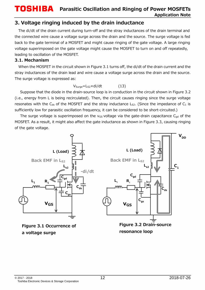
3. Voltage ringing induced by the drain inductance The di/dt of the drain current during turn-off and the stray inductances of the drain terminal and
the connected wire cause a voltage surge across the drain and the source. The surge voltage is fed back to the gate terminal of a MOSFET and might cause ringing of the gate voltage. A large ringing voltage superimposed on the gate voltage might cause the MOSFET to turn on and off repeatedly, leading to oscillation of the MOSFET. 3.1. Mechanism
When the MOSFET in the circuit shown in Figure 3.1 turns off, the di/dt of the drain current and the stray inductances of the drain lead and wire cause a voltage surge across the drain and the source. The surge voltage is expressed as:
VSurge=LS2×di/dt (13) Suppose that the diode in the drain-source loop is in conduction in the circuit shown in Figure 3.2
(i.e., energy from L is being recirculated). Then, the circuit causes ringing since the surge voltage resonates with the Cds of the MOSFET and the stray inductance LS2. (Since the impedance of C1 is sufficiently low for parasitic oscillation frequency, it can be considered to be short-circuited.)
The surge voltage is superimposed on the vGS voltage via the gate-drain capacitance Cgd of the MOSFET. As a result, it might also affect the gate inductance as shown in Figure 3.3, causing ringing of the gate voltage.
Figure 3.1 Occurrence of a voltage surge
Figure 3.2 Drain-source resonance loop
Cgs
Cgd
Cds
L (Load)
Ls2
L1 R1
vGS
-di/dt
Back EMF in LS2
Cgs
Cgd
Cds
L (Load)
Ls2
L1 R
1
C1
Back EMF in LS2
vGS
VDD

Parasitic Oscillation and Ringing of Power MOSFETs Application Note
2018-07-26 13 © 2017 - 2018 Toshiba Electronic Devices & Storage Corporation
3.2. Mitigating the ringing
In order to damp a surge voltage across the drain and source terminals, it is most important to reduce wire inductances. The amplitude of the surge voltage can also be reduced by increasing the gate resistance. In addition, the ringing of the gate voltage can be suppressed by reducing the gate stray inductance.
Figure 3.3 Ringing waveforms
VSurge
Ringing
Rise in VDS Drop of ID
VGS
ID
Parasitic Oscillation and Ringing of Power MOSFETs Application Note
2018-07-26 14 © 2017 - 2018 Toshiba Electronic Devices & Storage Corporation
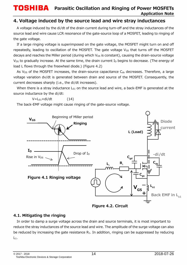
4. Voltage induced by the source lead and wire stray inductances A voltage induced by the di/dt of the drain current during turn-off and the stray inductances of the
source lead and wire cause LCR resonance of the gate-source loop of a MOSFET, leading to ringing of the gate voltage.
If a large ringing voltage is superimposed on the gate voltage, the MOSFET might turn on and off repeatedly, leading to oscillation of the MOSFET. The gate voltage VGS that turns off the MOSFET decays and reaches the Miller period (during which VGS is constant), causing the drain-source voltage VDS to gradually increase. At the same time, the drain current ID begins to decrease. (The energy of load L flows through the freewheel diode.) (Figure 4.2)
As VDS of the MOSFET increases, the drain-source capacitance Cds decreases. Therefore, a large voltage variation dv/dt is generated between drain and source of the MOSFET. Consequently, the current decreases sharply (i.e., the di/dt increases).
When there is a stray inductance LS1 on the source lead and wire, a back-EMF is generated at the source inductance by the di/dt:
V=LS1×di/dt (14) The back-EMF voltage might cause ringing of the gate-source voltage.
4.1. Mitigating the ringing
In order to damp a surge voltage across the drain and source terminals, it is most important to reduce the stray inductances of the source lead and wire. The amplitude of the surge voltage can also be reduced by increasing the gate resistance R1. In addition, ringing can be suppressed by reducing L1.
Figure 4.2. Circuit
Figure 4.1 Ringing voltage
Ringing
Beginning of Miller period
Rise in VDS Drop of ID
VGS
ID
Cgs
Cgd
Cds
L (Load)
L1
R1
Ls1
+
_
-di/dt
Diode current
Back EMF in Ls1
VGS

Parasitic Oscillation and Ringing of Power MOSFETs Application Note
2018-07-26 15 © 2017 - 2018 Toshiba Electronic Devices & Storage Corporation
Cgs
Cgd Cds
500μH
Ls2
L1
R1
Ls1
300V
10V
D
+
_
ID
vGS v
GS(L)
vDS
5. Simulating and reducing oscillation and ringing of a MOSFET We simulated to find out how the oscillation and ringing phenomena occur
and how to mitigate them. Since the purpose of this simulation was to investigate the
phenomena, the actual component values to be used are different.
5.1. Oscillator 5.1.1. Oscillation phenomenon
The oscillation of a circuit shown in Figure 5.1 was analyzed using the following component values. These are component values that caused oscillation. In order to simulate oscillation, the gate stray inductance L1 and the gate resistance were intentionally set to zero.
Drain stray inductance LS2=20 nH Source stray inductance: LS1=20 nH Gate stray inductance L1=0 nH Gate resistance R1=0 Ω
Figure 5.2 shows the waveforms of the gate voltage, drain voltage and drain current of the
MOSFET. Figure 5.2 Oscillation waveforms
Figure 5.1 Test circuit for oscillation
t (μs)
between gate and GND @LS1=20 nH, LS2=20 nH
t (μs)
t (μs)
between gate and source @LS1=20 nH, LS2=20 nH
@LS1=20 nH, LS2=20 nH
v GS(
L) (V
)
v GS (
V)
v DS
(V)
i D (A
)
iD vDS
Parasitic Oscillation and Ringing of Power MOSFETs Application Note
2018-07-26 16 © 2017 - 2018 Toshiba Electronic Devices & Storage Corporation
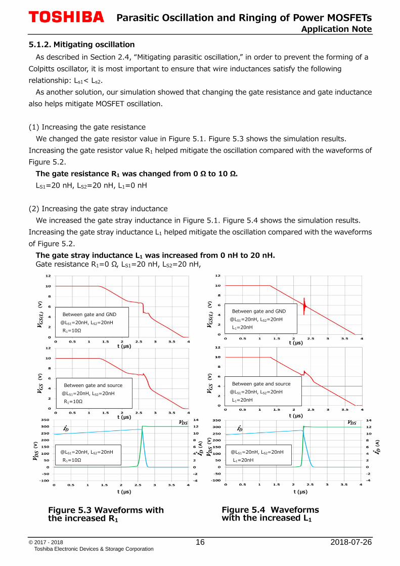
5.1.2. Mitigating oscillation As described in Section 2.4, “Mitigating parasitic oscillation,” in order to prevent the forming of a
Colpitts oscillator, it is most important to ensure that wire inductances satisfy the following relationship: Ls1< Ls2.
As another solution, our simulation showed that changing the gate resistance and gate inductance also helps mitigate MOSFET oscillation. (1) Increasing the gate resistance
We changed the gate resistor value in Figure 5.1. Figure 5.3 shows the simulation results. Increasing the gate resistor value R1 helped mitigate the oscillation compared with the waveforms of Figure 5.2.
The gate resistance R1 was changed from 0 Ω to 10 Ω. LS1=20 nH, LS2=20 nH, L1=0 nH
(2) Increasing the gate stray inductance
We increased the gate stray inductance in Figure 5.1. Figure 5.4 shows the simulation results. Increasing the gate stray inductance L1 helped mitigate the oscillation compared with the waveforms of Figure 5.2.
The gate stray inductance L1 was increased from 0 nH to 20 nH. Gate resistance R1=0 Ω, LS1=20 nH, LS2=20 nH,
Figure 5.3 Waveforms with the increased R1
Figure 5.4 Waveforms with the increased L1
t (μs) vDS vDS
Between gate and GND @LS1=20nH, LS2=20nH R1=10Ω
Between gate and source @LS1=20nH, LS2=20nH R1=10Ω
@LS1=20nH, LS2=20nH R1=10Ω
t (μs)
t (μs)
Between gate and GND @LS1=20nH, LS2=20nH L1=20nH
Between gate and source @LS1=20nH, LS2=20nH L1=20nH
@LS1=20nH, LS2=20nH L1=20nH
t (μs)
t (μs)
t (μs)
v GS(
L) (V
)
v GS(
L) (V
)
v GS (
V)
v GS (
V)
v DS (
V)
v DS (
V)
i D (A
)
i D (A
)
iD iD
Parasitic Oscillation and Ringing of Power MOSFETs Application Note
2018-07-26 17 © 2017 - 2018 Toshiba Electronic Devices & Storage Corporation
Cgs
Cgd
Cds
500μH
Ls2
L1
R1
300V
10V
D
+
_
ID
vGS
vDS
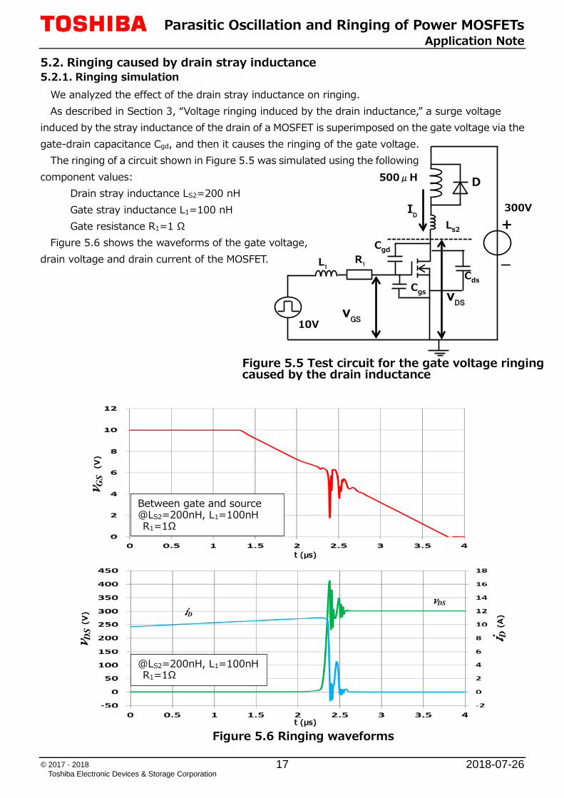
5.2. Ringing caused by drain stray inductance 5.2.1. Ringing simulation
We analyzed the effect of the drain stray inductance on ringing. As described in Section 3, “Voltage ringing induced by the drain inductance,” a surge voltage
induced by the stray inductance of the drain of a MOSFET is superimposed on the gate voltage via the gate-drain capacitance Cgd, and then it causes the ringing of the gate voltage.
The ringing of a circuit shown in Figure 5.5 was simulated using the following component values:
Drain stray inductance LS2=200 nH Gate stray inductance L1=100 nH Gate resistance R1=1 Ω
Figure 5.6 shows the waveforms of the gate voltage, drain voltage and drain current of the MOSFET.
Figure 5.5 Test circuit for the gate voltage ringing caused by the drain inductance
Figure 5.6 Ringing waveforms
Between gate and source @LS2=200nH, L1=100nH R1=1Ω
@LS2=200nH, L1=100nH R1=1Ω
t (μs)
t (μs)
v GS (
V)
v DS
(V)
i D (A
) iD vDS
Parasitic Oscillation and Ringing of Power MOSFETs Application Note
2018-07-26 18 © 2017 - 2018 Toshiba Electronic Devices & Storage Corporation
5.2.2. Mitigating the ringing As described in Section 3.2, “Mitigating the ringing,” the most important thing is to reduce the drain
stray inductance. As another solution, our simulation showed that changing the gate resistance and gate inductance
also helps mitigate the ringing caused by the drain stray inductance. (1) Increasing the gate resistance
We changed the gate resistor value in Figure 5.5. Figure 5.7 shows the simulation results. Increasing the gate resistor value R1 helped mitigate the ringing compared with the waveforms of Figure 5.6.
The gate resistance R1 was increased from 1 Ω to 10 Ω. LS2=200 nH, L1=100 nH
(2) Reducing the gate stray inductance
We reduced the gate stray inductance in Figure 5.5. Figure 5.8 shows the simulation results. Reducing the gate stray inductance L1 helped mitigate the ringing compared with the waveforms of Figure 5.6.
The gate stray inductance L1 was reduced from 100 nH to 10 nH. LS2=200 nH, R1=1 Ω
Figure 5.7 Waveforms with the increased R1
Figure 5.8 Waveforms with the reduced L1
vDS vDS
Between gate and source @LS2=200nH, L1=100nH R1=10Ω
@LS2=200nH, L1=100nH R1=10Ω
Between gate and source @LS2=200nH, L1=10nH R1=1Ω
@LS2=200nH L1=10nH, R1=1Ω
t (μs)
t (μs)
t (μs)
t (μs)
v GS (
V)
v GS (
V)
v DS
(V)
v DS
(V)
i D (A
)
i D (A
)
iD iD
Parasitic Oscillation and Ringing of Power MOSFETs Application Note
2018-07-26 19 © 2017 - 2018 Toshiba Electronic Devices & Storage Corporation
Figure 5.9 Test circuit for gate voltage ringing caused by the source inductance
Cgs
Cgd Cds
500μH
L1 R
1
Ls1
300V
10V
D
+
_
ID
vGS v
GS(L)
vDS
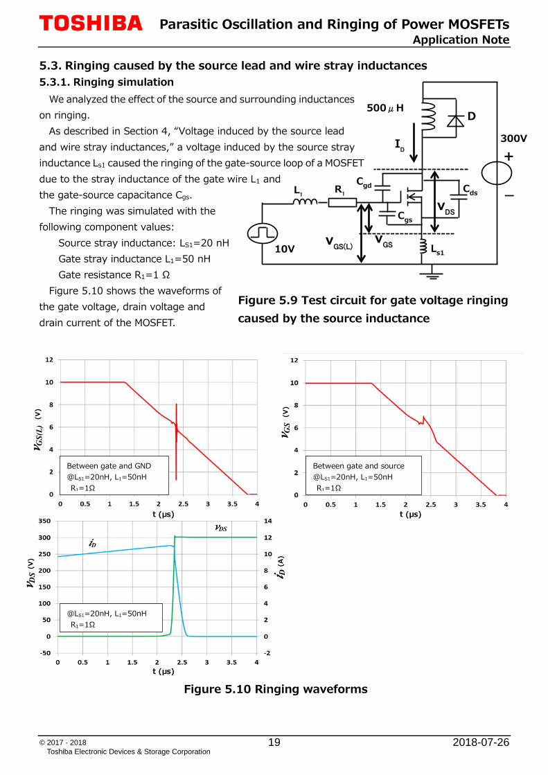
5.3. Ringing caused by the source lead and wire stray inductances 5.3.1. Ringing simulation
We analyzed the effect of the source and surrounding inductances on ringing.
As described in Section 4, “Voltage induced by the source lead and wire stray inductances,” a voltage induced by the source stray inductance Ls1 caused the ringing of the gate-source loop of a MOSFET due to the stray inductance of the gate wire L1 and the gate-source capacitance Cgs.
The ringing was simulated with the following component values: Source stray inductance: LS1=20 nH
Gate stray inductance L1=50 nH Gate resistance R1=1 Ω
Figure 5.10 shows the waveforms of the gate voltage, drain voltage and drain current of the MOSFET.
Figure 5.10 Ringing waveforms
Between gate and GND @LS1=20nH, L1=50nH R1=1Ω
Between gate and source @LS1=20nH, L1=50nH R1=1Ω
@LS1=20nH, L1=50nH R1=1Ω
t (μs) t (μs)
t (μs)
v GS(
L) (V
)
v GS (
V)
v DS
(V)
i D (A
)
iD vDS
Parasitic Oscillation and Ringing of Power MOSFETs Application Note
2018-07-26 20 © 2017 - 2018 Toshiba Electronic Devices & Storage Corporation
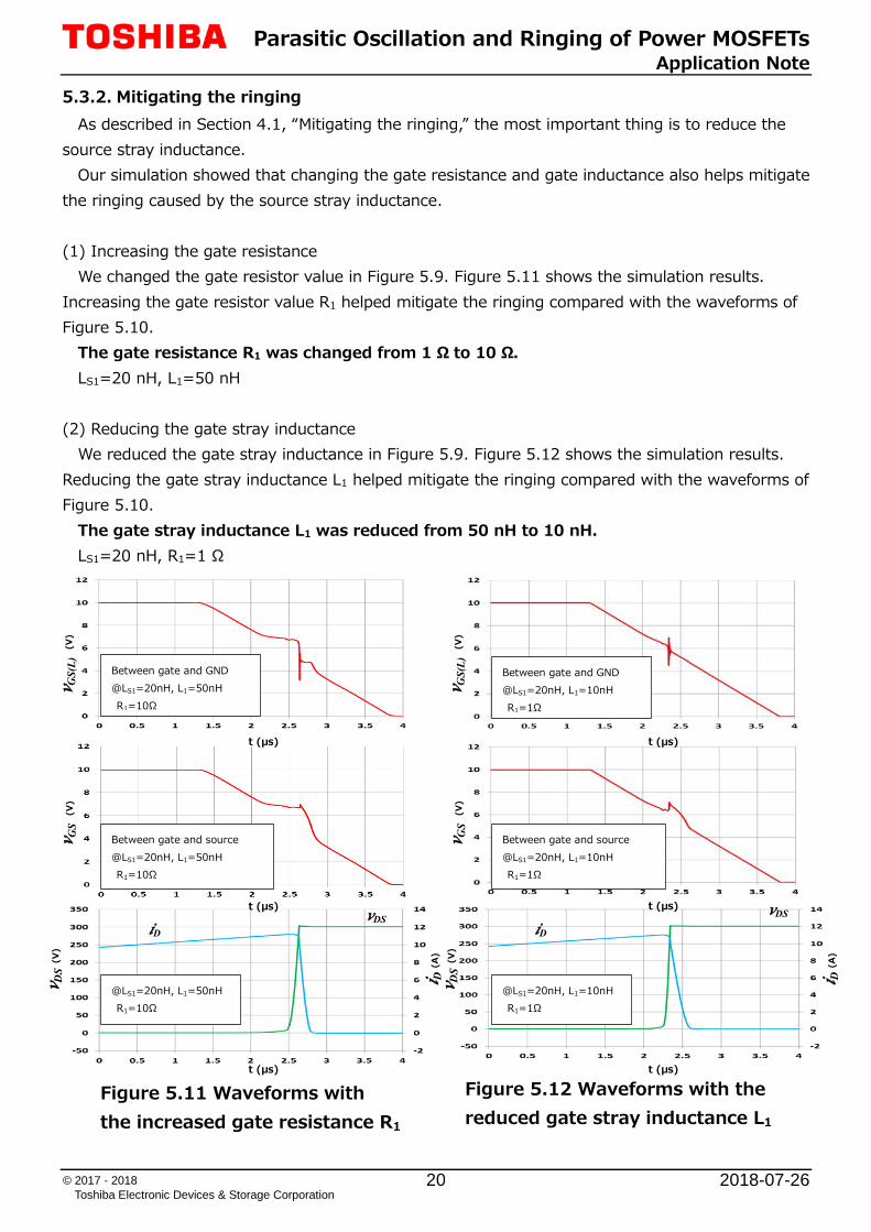
5.3.2. Mitigating the ringing As described in Section 4.1, “Mitigating the ringing,” the most important thing is to reduce the
source stray inductance. Our simulation showed that changing the gate resistance and gate inductance also helps mitigate
the ringing caused by the source stray inductance. (1) Increasing the gate resistance
We changed the gate resistor value in Figure 5.9. Figure 5.11 shows the simulation results. Increasing the gate resistor value R1 helped mitigate the ringing compared with the waveforms of Figure 5.10.
The gate resistance R1 was changed from 1 Ω to 10 Ω. LS1=20 nH, L1=50 nH
(2) Reducing the gate stray inductance
We reduced the gate stray inductance in Figure 5.9. Figure 5.12 shows the simulation results. Reducing the gate stray inductance L1 helped mitigate the ringing compared with the waveforms of Figure 5.10.
The gate stray inductance L1 was reduced from 50 nH to 10 nH. LS1=20 nH, R1=1 Ω
Figure 5.11 Waveforms with the increased gate resistance R1
Figure 5.12 Waveforms with the reduced gate stray inductance L1
vDS vDS
Between gate and GND @LS1=20nH, L1=50nH R1=10Ω
Between gate and source @LS1=20nH, L1=50nH R1=10Ω
@LS1=20nH, L1=50nH R1=10Ω
Between gate and GND @LS1=20nH, L1=10nH R1=1Ω
Between gate and source @LS1=20nH, L1=10nH R1=1Ω
@LS1=20nH, L1=10nH R1=1Ω
t (μs)
t (μs)
t (μs)
t (μs)
t (μs)
t (μs)
v GS(
L) (V
)
v GS(
L) (V
)
v GS (
V)
v GS (
V)
v DS (
V)
v DS (
V)
i D (A
)
i D (A
)
iD iD
Parasitic Oscillation and Ringing of Power MOSFETs Application Note
2018-07-26 21 © 2017 - 2018 Toshiba Electronic Devices & Storage Corporation
RESTRICTIONS ON PRODUCT USE Toshiba Corporation and its subsidiaries and affiliates are collectively referred to as “TOSHIBA”. Hardware, software and systems described in this document are collectively referred to as “Product”.
• TOSHIBA reserves the right to make changes to the information in this document and related Product without notice.
• This document and any information herein may not be reproduced without prior written permission from TOSHIBA. Even with TOSHIBA's written permission, reproduction is permissible only if reproduction is without alteration/omission.
• Though TOSHIBA works continually to improve Product's quality and reliability, Product can malfunction or fail. Customers are responsible for complying with safety standards and for providing adequate designs and safeguards for their hardware, software and systems which minimize risk and avoid situations in which a malfunction or failure of Product could cause loss of human life, bodily injury or damage to property, including data loss or corruption. Before customers use the Product, create designs including the Product, or incorporate the Product into their own applications, customers must also refer to and comply with (a) the latest versions of all relevant TOSHIBA information, including without limitation, this document, the specifications, the data sheets and application notes for Product and the precautions and conditions set forth in the "TOSHIBA Semiconductor Reliability Handbook" and (b) the instructions for the application with which the Product will be used with or for. Customers are solely responsible for all aspects of their own product design or applications, including but not limited to (a) determining the appropriateness of the use of this Product in such design or applications; (b) evaluating and determining the applicability of any information contained in this document, or in charts, diagrams, programs, algorithms, sample application circuits, or any other referenced documents; and (c) validating all operating parameters for such designs and applications. TOSHIBA ASSUMES NO LIABILITY FOR CUSTOMERS' PRODUCT DESIGN OR APPLICATIONS.
• PRODUCT IS NEITHER INTENDED NOR WARRANTED FOR USE IN EQUIPMENTS OR SYSTEMS THAT REQUIRE EXTRAORDINARILY HIGH LEVELS OF QUALITY AND/OR RELIABILITY, AND/OR A MALFUNCTION OR FAILURE OF WHICH MAY CAUSE LOSS OF HUMAN LIFE, BODILY INJURY, SERIOUS PROPERTY DAMAGE AND/OR SERIOUS PUBLIC IMPACT ("UNINTENDED USE"). Except for specific applications as expressly stated in this document, Unintended Use includes, without limitation, equipment used in nuclear facilities, equipment used in the aerospace industry, medical equipment, equipment used for automobiles, trains, ships and other transportation, traffic signaling equipment, equipment used to control combustions or explosions, safety devices, elevators and escalators, devices related to electric power, and equipment used in finance-related fields. IF YOU USE PRODUCT FOR UNINTENDED USE, TOSHIBA ASSUMES NO LIABILITY FOR PRODUCT. For details, please contact your TOSHIBA sales representative.
• Do not disassemble, analyze, reverse-engineer, alter, modify, translate or copy Product, whether in whole or in part.
• Product shall not be used for or incorporated into any products or systems whose manufacture, use, or sale is prohibited under any applicable laws or regulations.
• The information contained herein is presented only as guidance for Product use. No responsibility is assumed by TOSHIBA for any infringement of patents or any other intellectual property rights of third parties that may result from the use of Product. No license to any intellectual property right is granted by this document, whether express or implied, by estoppel or otherwise.
• ABSENT A WRITTEN SIGNED AGREEMENT, EXCEPT AS PROVIDED IN THE RELEVANT TERMS AND CONDITIONS OF SALE FOR PRODUCT, AND TO THE MAXIMUM EXTENT ALLOWABLE BY LAW, TOSHIBA (1) ASSUMES NO LIABILITY WHATSOEVER, INCLUDING WITHOUT LIMITATION, INDIRECT, CONSEQUENTIAL, SPECIAL, OR INCIDENTAL DAMAGES OR LOSS, INCLUDING WITHOUT LIMITATION, LOSS OF PROFITS, LOSS OF OPPORTUNITIES, BUSINESS INTERRUPTION AND LOSS OF DATA, AND (2) DISCLAIMS ANY AND ALL EXPRESS OR IMPLIED WARRANTIES AND CONDITIONS RELATED TO SALE, USE OF PRODUCT, OR INFORMATION, INCLUDING WARRANTIES OR CONDITIONS OF MERCHANTABILITY, FITNESS FOR A PARTICULAR PURPOSE, ACCURACY OF INFORMATION, OR NONINFRINGEMENT.
• Do not use or otherwise make available Product or related software or technology for any military purposes, including without limitation, for the design, development, use, stockpiling or manufacturing of nuclear, chemical, or biological weapons or missile technology products (mass destruction weapons). Product and related software and technology may be controlled under the applicable export laws and regulations including, without limitation, the Japanese Foreign Exchange and Foreign Trade Law and the U.S. Export Administration Regulations. Export and re-export of Product or related software or technology are strictly prohibited except in compliance with all applicable export laws and regulations.
• Please contact your TOSHIBA sales representative for details as to environmental matters such as the RoHS compatibility of Product. Please use Product in compliance with all applicable laws and regulations that regulate the inclusion or use of controlled substances, including without limitation, the EU RoHS Directive. TOSHIBA ASSUMES NO LIABILITY FOR DAMAGES OR LOSSES OCCURRING AS A RESULT OF NONCOMPLIANCE WITH APPLICABLE LAWS AND REGULATIONS.