Embed Size (px)
Citation preview
FN475Rev.6.00
Jan 13, 2017
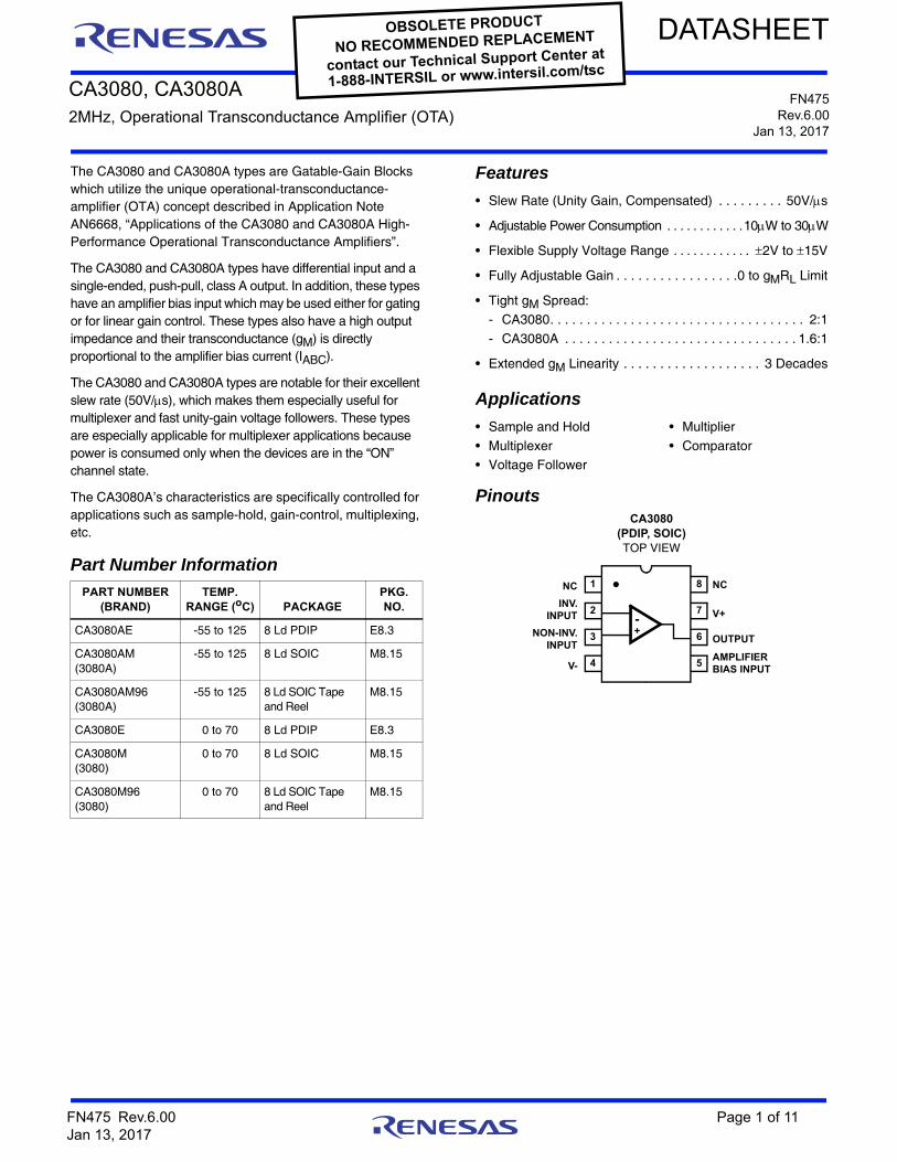
CA3080, CA3080A2MHz, Operational Transconductance Amplifier (OTA)
DATASHEETOBSOLETE PRODUCT
NO RECOMMENDED REPLACEMENT
contact our Technical Support Center at
1-888-INTERSIL or www.intersil.com/tsc
The CA3080 and CA3080A types are Gatable-Gain Blocks which utilize the unique operational-transconductance-amplifier (OTA) concept described in Application Note AN6668, “Applications of the CA3080 and CA3080A High-Performance Operational Transconductance Amplifiers”.
The CA3080 and CA3080A types have differential input and a single-ended, push-pull, class A output. In addition, these types have an amplifier bias input which may be used either for gating or for linear gain control. These types also have a high output impedance and their transconductance (gM) is directly proportional to the amplifier bias current (IABC).
The CA3080 and CA3080A types are notable for their excellent slew rate (50V/s), which makes them especially useful for multiplexer and fast unity-gain voltage followers. These types are especially applicable for multiplexer applications because power is consumed only when the devices are in the “ON” channel state.
The CA3080A’s characteristics are specifically controlled for applications such as sample-hold, gain-control, multiplexing, etc.
Features
• Slew Rate (Unity Gain, Compensated) . . . . . . . . . 50V/s
• Adjustable Power Consumption . . . . . . . . . . . .10W to 30W
• Flexible Supply Voltage Range . . . . . . . . . . . . 2V to 15V
• Fully Adjustable Gain . . . . . . . . . . . . . . . . .0 to gMRL Limit
• Tight gM Spread:- CA3080. . . . . . . . . . . . . . . . . . . . . . . . . . . . . . . . . . . 2:1
- CA3080A . . . . . . . . . . . . . . . . . . . . . . . . . . . . . . . . 1.6:1
• Extended gM Linearity . . . . . . . . . . . . . . . . . . . 3 Decades
Applications
• Sample and Hold • Multiplier
• Multiplexer • Comparator• Voltage Follower
PinoutsCA3080
(PDIP, SOIC)TOP VIEW
Part Number Information
PART NUMBER(BRAND)
TEMP. RANGE (oC) PACKAGE
PKG. NO.
CA3080AE -55 to 125 8 Ld PDIP E8.3
CA3080AM(3080A)
-55 to 125 8 Ld SOIC M8.15
CA3080AM96(3080A)
-55 to 125 8 Ld SOIC Tape and Reel
M8.15
CA3080E 0 to 70 8 Ld PDIP E8.3
CA3080M(3080)
0 to 70 8 Ld SOIC M8.15
CA3080M96(3080)
0 to 70 8 Ld SOIC Tape and Reel
M8.15
1
2
3
4
8
7
6
5
+
V+
NC
INV.INPUT
V-
NON-INV.INPUT
NC
OUTPUT
AMPLIFIERBIAS INPUT
-
FN475 Rev.6.00 Page 1 of 11Jan 13, 2017
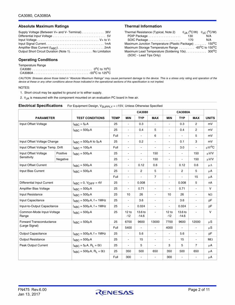
CA3080, CA3080A
Absolute Maximum Ratings Thermal Information
Supply Voltage (Between V+ and V- Terminal) . . . . . . . . . . . . . 36VDifferential Input Voltage . . . . . . . . . . . . . . . . . . . . . . . . . . . . . . . 5VInput Voltage . . . . . . . . . . . . . . . . . . . . . . . . . . . . . . . . . . . . V+ to V-Input Signal Current . . . . . . . . . . . . . . . . . . . . . . . . . . . . . . . . . . 1mAAmplifier Bias Current (IABC). . . . . . . . . . . . . . . . . . . . . . . . . . . 2mAOutput Short Circuit Duration (Note 1). . . . . . . . . . . . . No Limitation
Operating ConditionsTemperature RangeCA3080 . . . . . . . . . . . . . . . . . . . . . . . . . . . . . . . . . . . 0oC to 70oCCA3080A . . . . . . . . . . . . . . . . . . . . . . . . . . . . . . . . -55oC to 125oC
Thermal Resistance (Typical, Note 2) JA (oC/W) JC (oC/W)PDIP Package . . . . . . . . . . . . . . . . . . . 130 N/ASOIC Package . . . . . . . . . . . . . . . . . . . 170 N/A
Maximum Junction Temperature (Plastic Package) . . . . . . . 150oCMaximum Storage Temperature Range . . . . . . . . . -65oC to 150oCMaximum Lead Temperature (Soldering 10s) . . . . . . . . . . . . 300oC
(SOIC - Lead Tips Only)
CAUTION: Stresses above those listed in “Absolute Maximum Ratings” may cause permanent damage to the device. This is a stress only rating and operation of thedevice at these or any other conditions above those indicated in the operational sections of this specification is not implied.
NOTES:
1. Short circuit may be applied to ground or to either supply.
2. JA is measured with the component mounted on an evaluation PC board in free air.
Electrical Specifications For Equipment Design, VSUPPLY = 15V, Unless Otherwise Specified
PARAMETER TEST CONDITIONS TEMP
CA3080 CA3080A
UNITSMIN TYP MAX MIN TYP MAX
Input Offset Voltage IABC = 5A 25 - 0.3 - - 0.3 2 mV
IABC = 500A 25 - 0.4 5 - 0.4 2 mV
Full - - 6 - - 5 mV
Input Offset Voltage Change IABC = 500A to 5A 25 - 0.2 - - 0.1 3 mV
Input Offset Voltage Temp. Drift IABC = 100A Full - - - - 3.0 - V/oC
Input Offset Voltage Sensitivity
Positive IABC = 500A 25 - - 150 - - 150 V/V
Negative 25 - - 150 - - 150 V/V
Input Offset Current IABC = 500A 25 - 0.12 0.6 - 0.12 0.6
Input Bias Current IABC = 500A 25 - 2 5 - 2 5 A
Full - - 7 - - 15 A
Differential Input Current IABC = 0, VDIFF = 4V 25 - 0.008 - - 0.008 5 nA
Amplifier Bias Voltage IABC = 500A 25 - 0.71 - - 0.71 - V
Input Resistance IABC = 500A 25 10 26 - 10 26 - k
Input Capacitance IABC = 500A, f = 1MHz 25 - 3.6 - - 3.6 - pF
Input-to-Output Capacitance IABC = 500A, f = 1MHz 25 - 0.024 - - 0.024 - pF
Common-Mode Input-Voltage Range
IABC = 500A 25 12 to -12
13.6 to-14.6
- 12 to -12
13.6 to-14.6
- V
Forward Transconductance(Large Signal)
IABC = 500A 25 6700 9600 13000 7700 9600 12000 S
Full 5400 - - 4000 - - S
Output Capacitance IABC = 500Af = 1MHz 25 - 5.6 - - 5.6 - pF
Output Resistance IABC = 500A 25 - 15 - - 15 - M
Peak Output Current IABC = 5A, RL = 0 25 - 5 - 3 5 7 A
IABC = 500A, RL = 0 25 350 500 650 350 500 650 A
Full 300 - - 300 - - A
FN475 Rev.6.00 Page 2 of 11Jan 13, 2017
CA3080, CA3080A
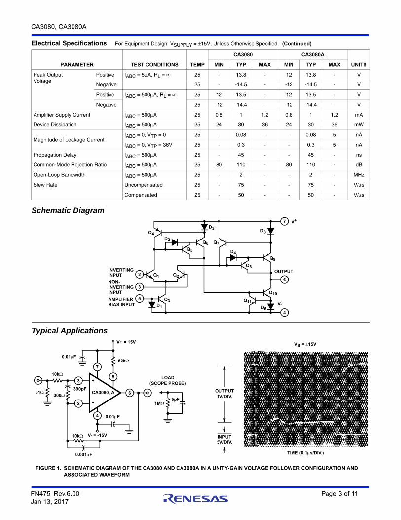
Schematic Diagram
Peak OutputVoltage
Positive IABC = 5A, RL = 25 - 13.8 - 12 13.8 - V
Negative 25 - -14.5 - -12 -14.5 - V
Positive IABC = 500A, RL = 25 12 13.5 - 12 13.5 - V
Negative 25 -12 -14.4 - -12 -14.4 - V
Amplifier Supply Current IABC = 500A 25 0.8 1 1.2 0.8 1 1.2 mA
Device Dissipation IABC = 500A 25 24 30 36 24 30 36 mW
Magnitude of Leakage CurrentIABC = 0, VTP = 0 25 - 0.08 - - 0.08 5 nA
IABC = 0, VTP = 36V 25 - 0.3 - - 0.3 5 nA
Propagation Delay IABC = 500A 25 - 45 - - 45 - ns
Common-Mode Rejection Ratio IABC = 500A 25 80 110 - 80 110 - dB
Open-Loop Bandwidth IABC = 500A 25 - 2 - - 2 - MHz
Slew Rate Uncompensated 25 - 75 - - 75 - V/s
Compensated 25 - 50 - - 50 - V/s
Typical Applications
FIGURE 1. SCHEMATIC DIAGRAM OF THE CA3080 AND CA3080A IN A UNITY-GAIN VOLTAGE FOLLOWER CONFIGURATION AND ASSOCIATED WAVEFORM
Electrical Specifications For Equipment Design, VSUPPLY = 15V, Unless Otherwise Specified (Continued)
PARAMETER TEST CONDITIONS TEMP
CA3080 CA3080A
UNITSMIN TYP MAX MIN TYP MAX
2OUTPUT
V+
AMPLIFIERBIAS INPUT
NON-INVERTINGINPUT
INVERTINGINPUT
3
5
4
6
7
V-
Q4D2
Q5
Q6 Q7
Q1 Q2
Q3D1
D4
D3
Q8
Q11D6
Q10
Q9
D3
5
2
4
7
5pF1M
LOAD(SCOPE PROBE)3
6CA3080, A51
0.01F
0.01F
390pF
300
V- = -15V
0.001F
62k
V+ = 15V
+
10k
-
10k
VS = 15V
TIME (0.1s/DIV.)
OUTPUT1V/DIV.
INPUT5V/DIV.
FN475 Rev.6.00 Page 3 of 11Jan 13, 2017
CA3080, CA3080A
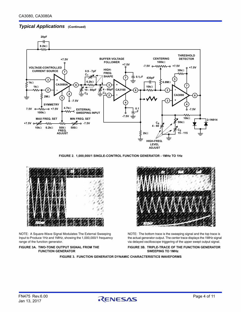
FIGURE 2. 1,000,000/1 SINGLE-CONTROL FUNCTION GENERATOR - 1MHz TO 1Hz
NOTE: A Square-Wave Signal Modulates The External Sweeping Input to Produce 1Hz and 1MHz, showing the 1,000,000/1 frequency range of the function generator.
NOTE: The bottom trace is the sweeping signal and the top trace is the actual generator output. The center trace displays the 1MHz signal via delayed oscilloscope triggering of the upper swept output signal.
FIGURE 3A. TWO-TONE OUTPUT SIGNAL FROM THE FUNCTION GENERATOR
FIGURE 3B. TRIPLE-TRACE OF THE FUNCTION GENERATOR SWEEPING TO 1MHz
FIGURE 3. FUNCTION GENERATOR DYNAMIC CHARACTERISTICS WAVEFORMS
Typical Applications (Continued)
7
4
7
5
4
4
7
6CA3160
3
2
6
8.2k
2
3
2
3
6
5
20pF
VOLTAGE-CONTROLLEDCURRENT SOURCE
+7.5V
CA3080A1k
1k
2M
100k7.5V +7.5V
SYMMETRY
MAX FREQ. SET
EXTERNALSWEEPING INPUT
+7.5V
10k 6.2k 500
-7.5V
MIN FREQ. SET
4.7k
-7.5V
0.9 - 7pFC1
6.2k
10 - 80pFC2
4 - 60pFC3
+
-
BUFFER VOLTAGEFOLLOWER
0.1F
0.1F
-7.5V
+7.5V
2k
10k
CENTERING100k
+7.5V-7.5V+7.5V
430pF
6.8M
CA3080
+
-
30k
-7.5V
10k50k
C515 - 115
C44 - 60
HIGH-FREQ.LEVEL
ADJUST
2-1N914
HIGH-FREQ.SHAPE
THRESHOLDDETECTOR
+
-
FREQ.ADJUST
500
FN475 Rev.6.00 Page 4 of 11Jan 13, 2017
CA3080, CA3080A
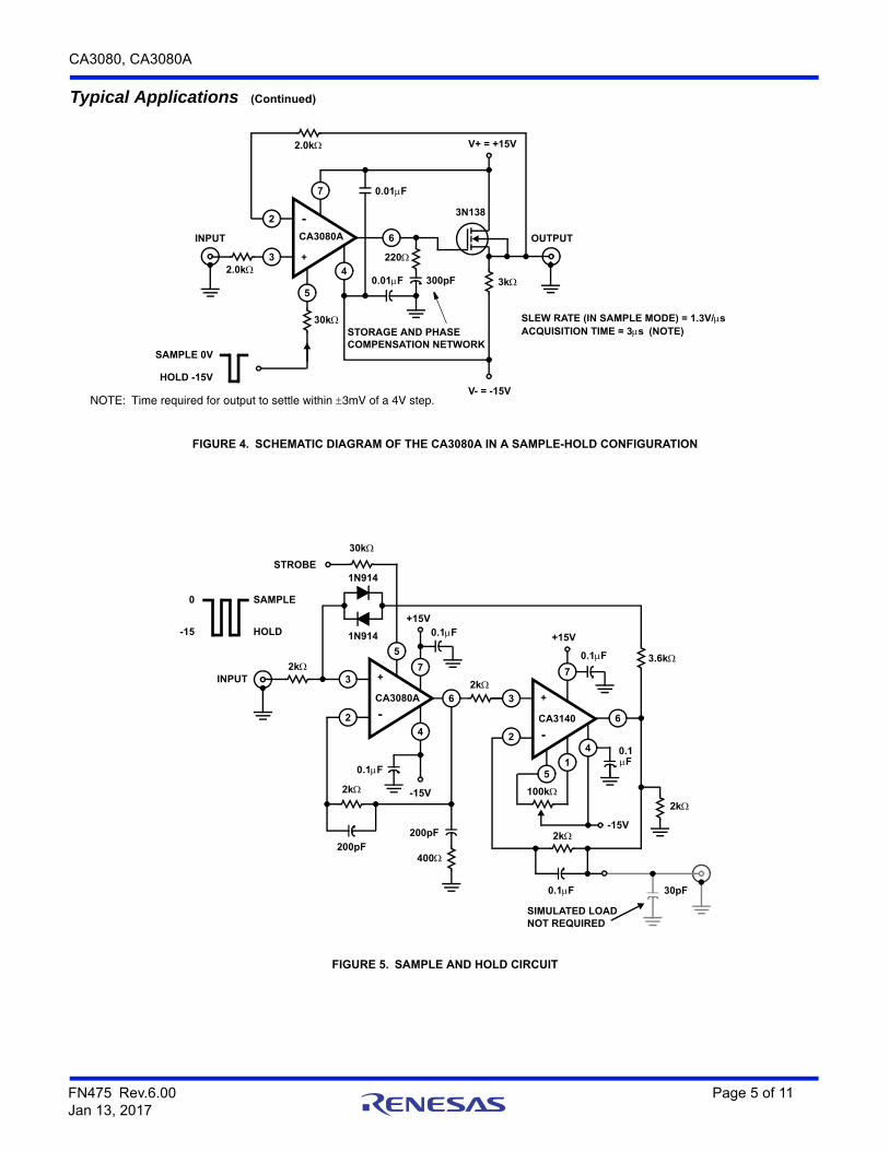
FIGURE 4. SCHEMATIC DIAGRAM OF THE CA3080A IN A SAMPLE-HOLD CONFIGURATION
FIGURE 5. SAMPLE AND HOLD CIRCUIT
Typical Applications (Continued)
7
4
2
6
5
3
CA3080A
+
-
2.0k
2.0k
30k
220
0.01F 300pF 3k
OUTPUTINPUT
0.01F
V- = -15V
V+ = +15V
3N138
SAMPLE 0V
HOLD -15V
STORAGE AND PHASECOMPENSATION NETWORK
SLEW RATE (IN SAMPLE MODE) = 1.3V/sACQUISITION TIME = 3s (NOTE)
NOTE: Time required for output to settle within 3mV of a 4V step.
5
2
CA3080A
+
-
7
4
3
6
5
2
CA3140
+
-4
7
6
INPUT 3
1
STROBE
30k
1N914
1N914
2k
+15V
-15V2k
200pF
200pF
400
2k
2k
3.6k
30pF
+15V
-15V2k
100k
0.1F
0.1F
0.1F
0.1F
0.1F
0
-15
SAMPLE
HOLD
SIMULATED LOADNOT REQUIRED
FN475 Rev.6.00 Page 5 of 11Jan 13, 2017
CA3080, CA3080A
Top Trace: Output Signal5V/Div., 2s/Div.
Bottom Trace: Input Signal5V/Div., 2s/Div.
Center Trace: Difference of Input and Output Signals ThroughTektronix Amplifier 7A135mV/Div., 2s/Div.
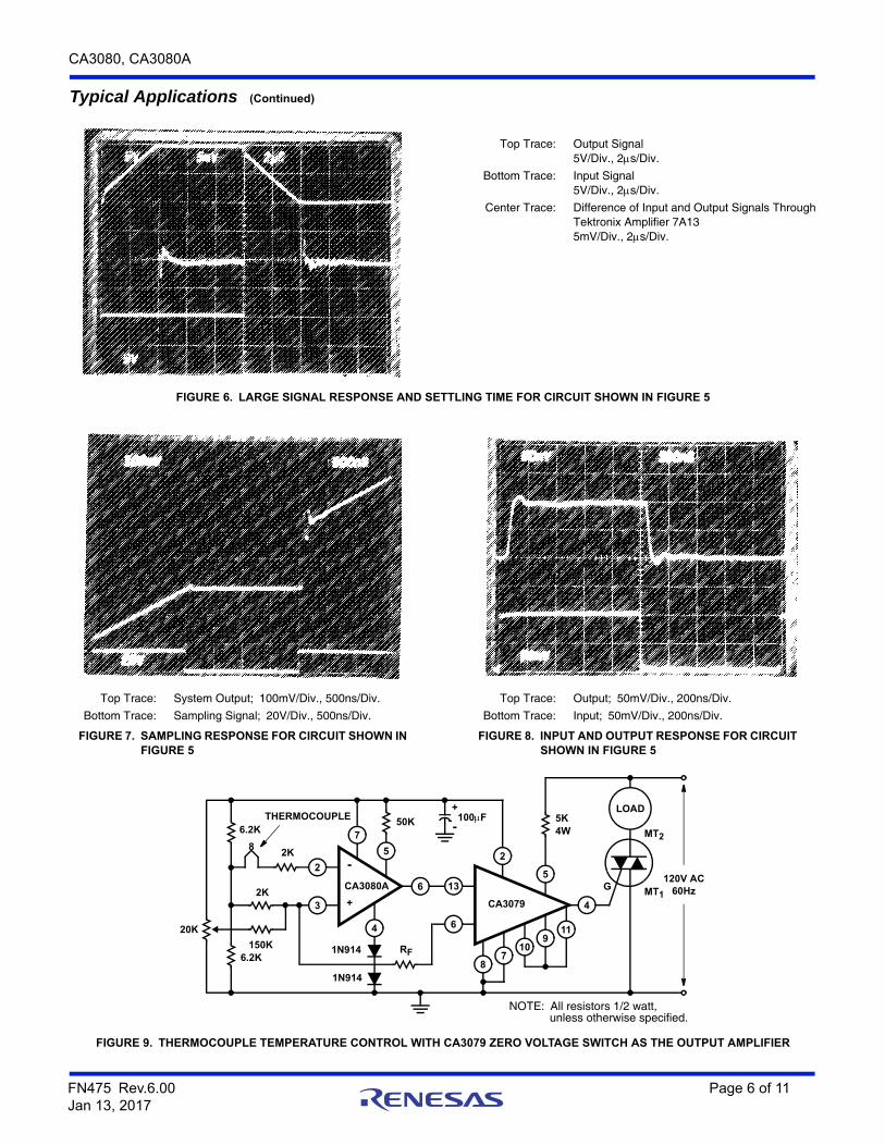
FIGURE 6. LARGE SIGNAL RESPONSE AND SETTLING TIME FOR CIRCUIT SHOWN IN FIGURE 5
Top Trace: System Output; 100mV/Div., 500ns/Div.
Bottom Trace: Sampling Signal; 20V/Div., 500ns/Div.
Top Trace: Output; 50mV/Div., 200ns/Div.
Bottom Trace: Input; 50mV/Div., 200ns/Div.
FIGURE 7. SAMPLING RESPONSE FOR CIRCUIT SHOWN IN FIGURE 5
FIGURE 8. INPUT AND OUTPUT RESPONSE FOR CIRCUIT SHOWN IN FIGURE 5
FIGURE 9. THERMOCOUPLE TEMPERATURE CONTROL WITH CA3079 ZERO VOLTAGE SWITCH AS THE OUTPUT AMPLIFIER
Typical Applications (Continued)
10
2
7
3
CA3080A
+
-
4
6
5
13
2
6
CA3079
8
4
5
7
911
LOAD
120V AC60Hz
MT2
MT1
5K4W
50K6.2K
2K
2K
150K6.2K
20K
1N914
1N914 RF
100F+
-
G
8
NOTE: All resistors 1/2 watt,unless otherwise specified.
THERMOCOUPLE
FN475 Rev.6.00 Page 6 of 11Jan 13, 2017
CA3080, CA3080A
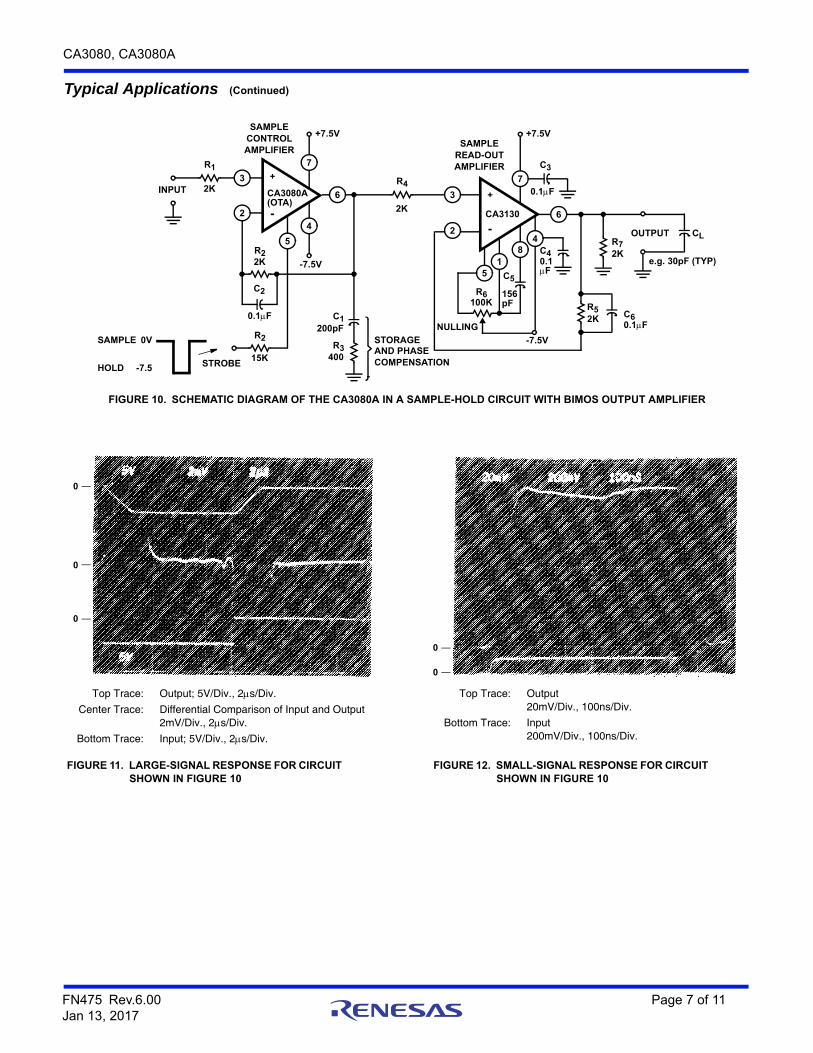
FIGURE 10. SCHEMATIC DIAGRAM OF THE CA3080A IN A SAMPLE-HOLD CIRCUIT WITH BIMOS OUTPUT AMPLIFIER
Top Trace: Output; 5V/Div., 2s/Div.
Center Trace: Differential Comparison of Input and Output2mV/Div., 2s/Div.
Bottom Trace: Input; 5V/Div., 2s/Div.
Top Trace: Output20mV/Div., 100ns/Div.
Bottom Trace: Input200mV/Div., 100ns/Div.
FIGURE 11. LARGE-SIGNAL RESPONSE FOR CIRCUIT SHOWN IN FIGURE 10
FIGURE 12. SMALL-SIGNAL RESPONSE FOR CIRCUIT SHOWN IN FIGURE 10
Typical Applications (Continued)
5
2
CA3080A
+
-
7
4
3
6
5
2
CA3130
+
-4
7
6
3
81
INPUT
R1
2K
+7.5V
-7.5V
R22K
C2
R2
15K
0.1F
STROBE
SAMPLECONTROLAMPLIFIER
C1200pF
R3400
STORAGEAND PHASECOMPENSATION
-7.5V
NULLING
R4
2K
SAMPLEREAD-OUTAMPLIFIER
+7.5V
C3
0.1F
C40.1F
C5
156pF R5
2K C60.1F
R72K
OUTPUT CL
e.g. 30pF (TYP)
SAMPLE
HOLD
0V
-7.5
(OTA)
R6100K
0
0
0
0
0
FN475 Rev.6.00 Page 7 of 11Jan 13, 2017
CA3080, CA3080A
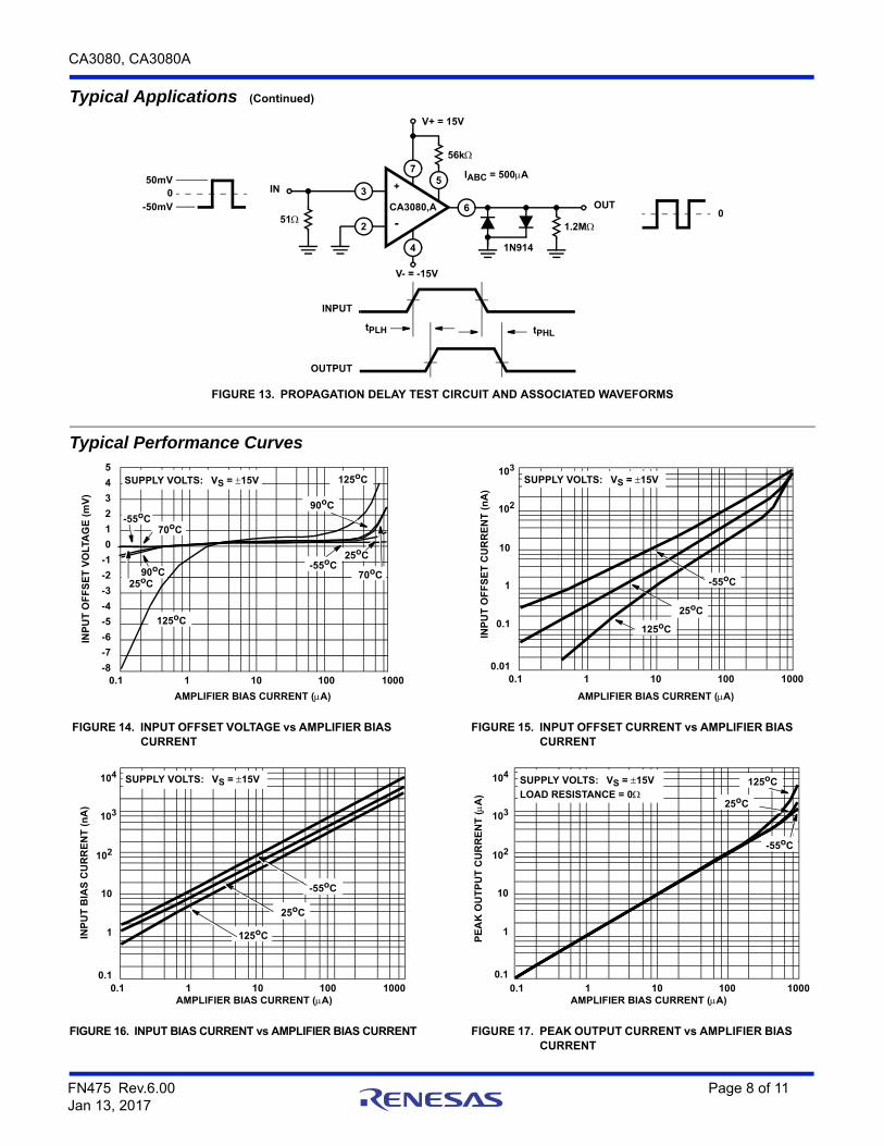
FIGURE 13. PROPAGATION DELAY TEST CIRCUIT AND ASSOCIATED WAVEFORMS
Typical Performance Curves
FIGURE 14. INPUT OFFSET VOLTAGE vs AMPLIFIER BIAS CURRENT
FIGURE 15. INPUT OFFSET CURRENT vs AMPLIFIER BIAS CURRENT
FIGURE 16. INPUT BIAS CURRENT vs AMPLIFIER BIAS CURRENT FIGURE 17. PEAK OUTPUT CURRENT vs AMPLIFIER BIAS CURRENT
Typical Applications (Continued)
INPUT
OUTPUT
tPLH tPHL
7
2
CA3080,A
+
-
4
5
6
3OUT
IN
51
V- = -15V
1N914
1.2M
IABC = 500A
56k
V+ = 15V
0
0-50mV
50mV
SUPPLY VOLTS: VS = 15V
70oC
125oC
90oC
-55oC 25oC
70oC
25oC
125oC
5
4
3
2
1
0
-1
-2
-3
-4
-5
-6
-7
-80.1 1 10 100 1000
INP
UT
OF
FS
ET
VO
LTA
GE
(m
V)
AMPLIFIER BIAS CURRENT (A)
90oC
-55oC
SUPPLY VOLTS: VS = 15V
-55oC
25oC
125oC
103
0.1 1 10 100 1000
INP
UT
OF
FS
ET
CU
RR
EN
T (
nA
)
AMPLIFIER BIAS CURRENT (A)
102
10
1
0.1
0.01
SUPPLY VOLTS: VS = 15V
-55oC
25oC
125oC
104
0.1 1 10 100 1000
INP
UT
BIA
S C
UR
RE
NT
(n
A)
AMPLIFIER BIAS CURRENT (A)
103
102
10
1
0.10.1 1 10 100 1000
AMPLIFIER BIAS CURRENT (A)
104
PE
AK
OU
TP
UT
CU
RR
EN
T (A
)
103
102
10
1
0.1
SUPPLY VOLTS: VS = 15V
-55oC
25oC
125oCLOAD RESISTANCE = 0
FN475 Rev.6.00 Page 8 of 11Jan 13, 2017
CA3080, CA3080A
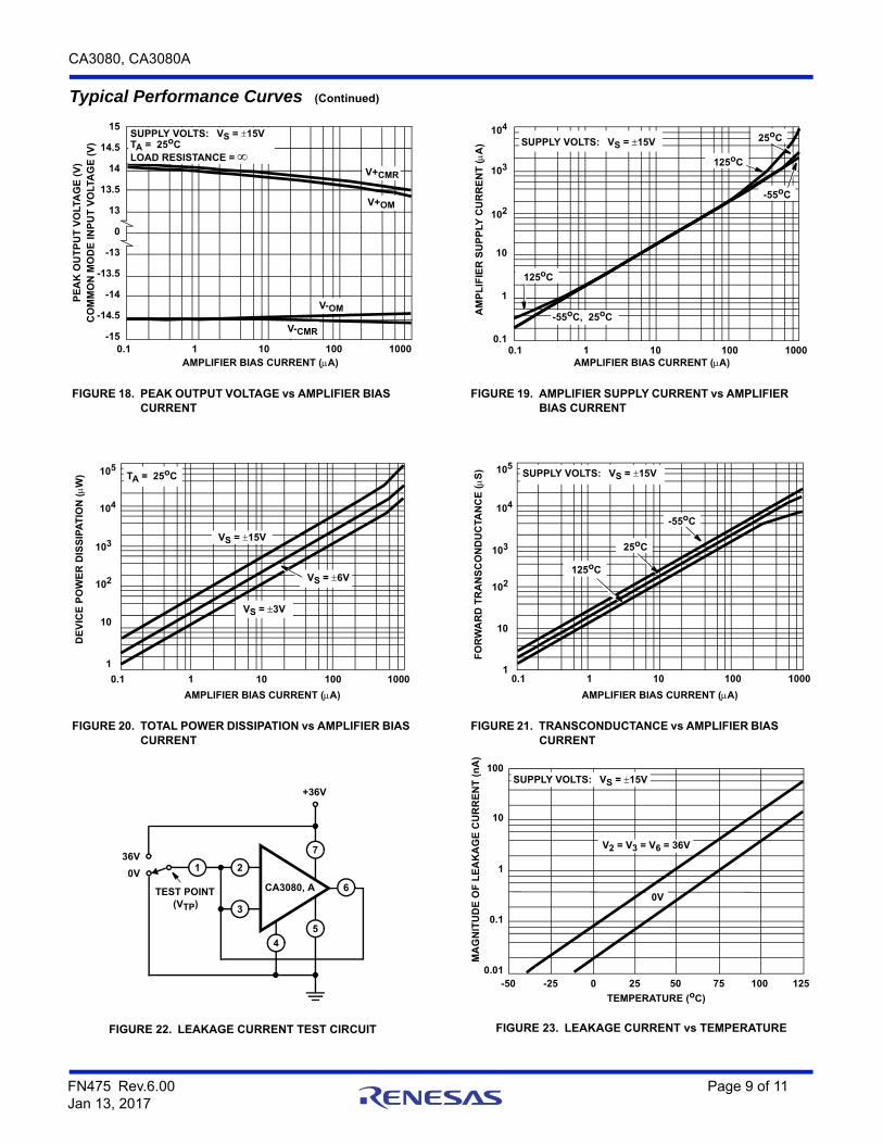
FIGURE 18. PEAK OUTPUT VOLTAGE vs AMPLIFIER BIAS CURRENT
FIGURE 19. AMPLIFIER SUPPLY CURRENT vs AMPLIFIER BIAS CURRENT
FIGURE 20. TOTAL POWER DISSIPATION vs AMPLIFIER BIAS CURRENT
FIGURE 21. TRANSCONDUCTANCE vs AMPLIFIER BIAS CURRENT
FIGURE 22. LEAKAGE CURRENT TEST CIRCUIT FIGURE 23. LEAKAGE CURRENT vs TEMPERATURE
Typical Performance Curves (Continued)
SUPPLY VOLTS: VS = 15VTA = 25oCLOAD RESISTANCE =
15
14.5
14
13.5
13
0
-13
-13.5
-14
-14.5
-150.1 1 10 100 1000
AMPLIFIER BIAS CURRENT (A)
V+OM
V+CMR
V-OM
V-CMR
PE
AK
OU
TP
UT
VO
LTA
GE
(V
)C
OM
MO
N M
OD
E I
NP
UT
VO
LTA
GE
(V
)
0.1 1 10 100 1000AMPLIFIER BIAS CURRENT (A)
SUPPLY VOLTS: VS = 15V
-55oC
25oC
125oC
104
AM
PL
IFIE
R S
UP
PLY
CU
RR
EN
T (A
)
103
102
10
1
0.1
125oC
-55oC, 25oC
TA = 25oC
VS = 15V
VS = 6V
VS = 3V
105
104
103
102
10
1
DE
VIC
E P
OW
ER
DIS
SIP
AT
ION
(W
)
0.1 1 10 100 1000
AMPLIFIER BIAS CURRENT (A)
0.1 1 10 100 1000
AMPLIFIER BIAS CURRENT (A)
SUPPLY VOLTS: VS = 15V
-55oC
25oC
105
104
103
102
10
1
125oC
FO
RW
AR
D T
RA
NS
CO
ND
UC
TAN
CE
(S
)
2
3
4
6
1
CA3080, A
5
736V
0V
TEST POINT(VTP)
+36V
-50 0 25 75 125
TEMPERATURE (oC)
SUPPLY VOLTS: VS = 15V100
10
1
0.1
0.01
V2 = V3 = V6 = 36V
0V
-25 50 100
MA
GN
ITU
DE
OF
LE
AK
AG
E C
UR
RE
NT
(n
A)
FN475 Rev.6.00 Page 9 of 11Jan 13, 2017
CA3080, CA3080A
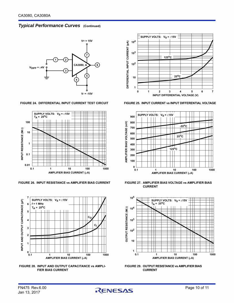
FIGURE 24. DIFFERENTIAL INPUT CURRENT TEST CIRCUIT FIGURE 25. INPUT CURRENT vs INPUT DIFFERENTIAL VOLTAGE
FIGURE 26. INPUT RESISTANCE vs AMPLIFIER BIAS CURRENT FIGURE 27. AMPLIFIER BIAS VOLTAGE vs AMPLIFIER BIAS CURRENT
FIGURE 28. INPUT AND OUTPUT CAPACITANCE vs AMPLI-FIER BIAS CURRENT
FIGURE 29. OUTPUT RESISTANCE vs AMPLIFIER BIAS CURRENT
Typical Performance Curves (Continued)
5
7
V+ = 15V
CA3080, A
2
3
4
6
1
VDIFF = 4V
V- = -15V
SUPPLY VOLTS: VS = 15V
25oC
125oC
0 1 2 3 4 5 6 7
10
1
102
103
104
DIF
FE
RE
NT
IAL
IN
PU
T C
UR
RE
NT
(p
A)
INPUT DIFFERENTIAL VOLTAGE (V)
SUPPLY VOLTS: VS = 15VTA = 25oC
INP
UT
RE
SIS
TAN
CE
(M
)
100
10
1
0.1
0.010.1 1 10 100 1000
AMPLIFIER BIAS CURRENT (A)
SUPPLY VOLTS: VS = 15V
-55oC
25oC
125oC
0.1 1 10 100 1000AMPLIFIER BIAS CURRENT (A)
900
800
700
600
500
400
300
200
100
0
AM
PL
IFIE
R B
IAS
VO
LTA
GE
(m
V)
SUPPLY VOLTS: VS = 15V
0.1 1 10 100 1000AMPLIFIER BIAS CURRENT (A)
6
5
4
3
2
1
0
7
f = 1 MHz
TA = 25oC
INP
UT
AN
D O
UT
PU
T C
AP
AC
ITA
NC
E (
pF
)
CI
CO
0.1 1 10 100 1000AMPLIFIER BIAS CURRENT (A)
104
103
102
10
1
105
OU
TP
UT
RE
SIS
TAN
CE
(M
)
SUPPLY VOLTS: VS = 15VTA = 25oC
FN475 Rev.6.00 Page 10 of 11Jan 13, 2017
CA3080, CA3080A
Intersil products are manufactured, assembled and tested utilizing ISO9001 quality systems as notedin the quality certifications found at www.intersil.com/en/support/qualandreliability.html
Intersil products are sold by description only. Intersil may modify the circuit design and/or specifications of products at any time without notice, provided that such modification does not, in Intersil's sole judgment, affect the form, fit or function of the product. Accordingly, the reader is cautioned to verify that datasheets are current before placing orders. Information furnished by Intersil is believed to be accurate and reliable. However, no responsibility is assumed by Intersil or its subsidiaries for its use; nor for any infringements of patents or other rights of third parties which may result from its use. No license is granted by implication or otherwise under any patent or patent rights of Intersil or its subsidiaries.
For information regarding Intersil Corporation and its products, see www.intersil.com
For additional products, see www.intersil.com/en/products.html
© Copyright Intersil Americas LLC 2001-2004. All Rights Reserved.All trademarks and registered trademarks are the property of their respective owners.
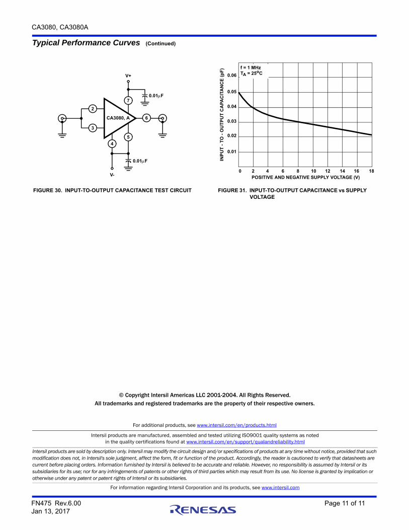
FIGURE 30. INPUT-TO-OUTPUT CAPACITANCE TEST CIRCUIT FIGURE 31. INPUT-TO-OUTPUT CAPACITANCE vs SUPPLY VOLTAGE
Typical Performance Curves (Continued)
5
7
V+
2
3
4
V-
CA3080, A
0.01F
6
0.01F
f = 1 MHzTA = 25oC0.06
0.05
0.04
0.03
0.02
0.01
0 2 4 6 8 10 12 14 16 18
INP
UT
- T
O -
OU
TP
UT
CA
PA
CIT
AN
CE
(p
F)
POSITIVE AND NEGATIVE SUPPLY VOLTAGE (V)
FN475 Rev.6.00 Page 11 of 11Jan 13, 2017


![Operational Transconductance Amplifier (OTA) in 45nm CMOS · Amplifier (OTA) in 45nm CMOS YOUNGSEOK LEE ... Design of Analog CMOS Integrated Circuits. McGraw-Hill, 2002. [2] B. Ahuja,](https://img.pdfslide.net/doc/110x75/5fbfc7035b7a87264a188ff5/operational-transconductance-amplifier-ota-in-45nm-cmos-amplifier-ota-in-45nm.jpg)
![A Built in Self Test System for Dynamic Performance ... · the test stimulus an oscillator circuit can be used [7]. The Operational Transconductance Amplifier and Capacitor (OTA-C)](https://img.pdfslide.net/doc/110x75/5fc768800c90ea5d227f0137/a-built-in-self-test-system-for-dynamic-performance-the-test-stimulus-an-oscillator.jpg)