Embed Size (px)
Citation preview
Miss. Niveditha Yadav M. Int. Journal of Engineering Research and Application www.ijera.com
ISSN : 2248-9622, Vol. 7, Issue 5, ( Part -5) May 2017, pp.11-16
www.ijera.com DOI: 10.9790/9622-0705051116 11 | P a g e
A Design of Sigma-Delta ADC Using OTA
Miss. Niveditha Yadav M1, Mr. Yaseen Basha
2, Dr. Venkatesh kumar H
3
1Department of ECE, PG Student, NCET/VTU, and Bengaluru, India
2Department of ECE, Assistant professor, NCET/VTU, India, Bengaluru 3Department of ECE, Associate professor, NCET/VTU, India, Bengaluru
ABSTRACT Sigma-Delta Analog-to-Digital converter (ADC), is widely used in portable electronic products. An operational
transconductance amplifier (OTA) is one of the most important components of ADC. This paper presents a
new design of two stages OTA. The design incorporates Sleep insertion technique and leakage feedback current
approach for improving design parameters such as gain, and power as compared to earlier work. The design is
simulated in 0.18µm CMOS technology with supply voltage 1.8V.
Keywords: ADC, OTA, Sleep insertion Technique, Leakage feedback approach.
I. INTRODUCTION Modern VLSI devices demands for
excessive information value with low energy
consumption and needless speed. The key additives
in the wireless receiver is the ADC, it is far way a
margin in the middle of analog and digital design.
Operational Transconductance Amplifier
The OTA is a basic building blocks found
in many analog devices such as data converter’s
(ADC &DAC). The OTA is a Transconductance
device in which the input voltage controls the output
current, it means that OTA is a voltage controlled
current source whereas the op-amps are voltage
controlled voltage source. An OTA is basically an
opamp without output buffer, so it can only drive
loads.
Analog-to-digital converter
ADC is a fundamental block in mixed-
signal VLSI circuits. The rapid growth of mobile
electronic systems increases the demand for
developing low-cost and low-power circuit
technique with high performance. Sigma delta (ΣΔ)
modulators are one of the preferred architectures for
high resolution converters. Power consumption and
area are the key parameters for a sigma delta
modulator these parameters cannot be changed once
an ADC is designed. While it can operate at higher
speed and will consume less power when operating
at a lower resolution.
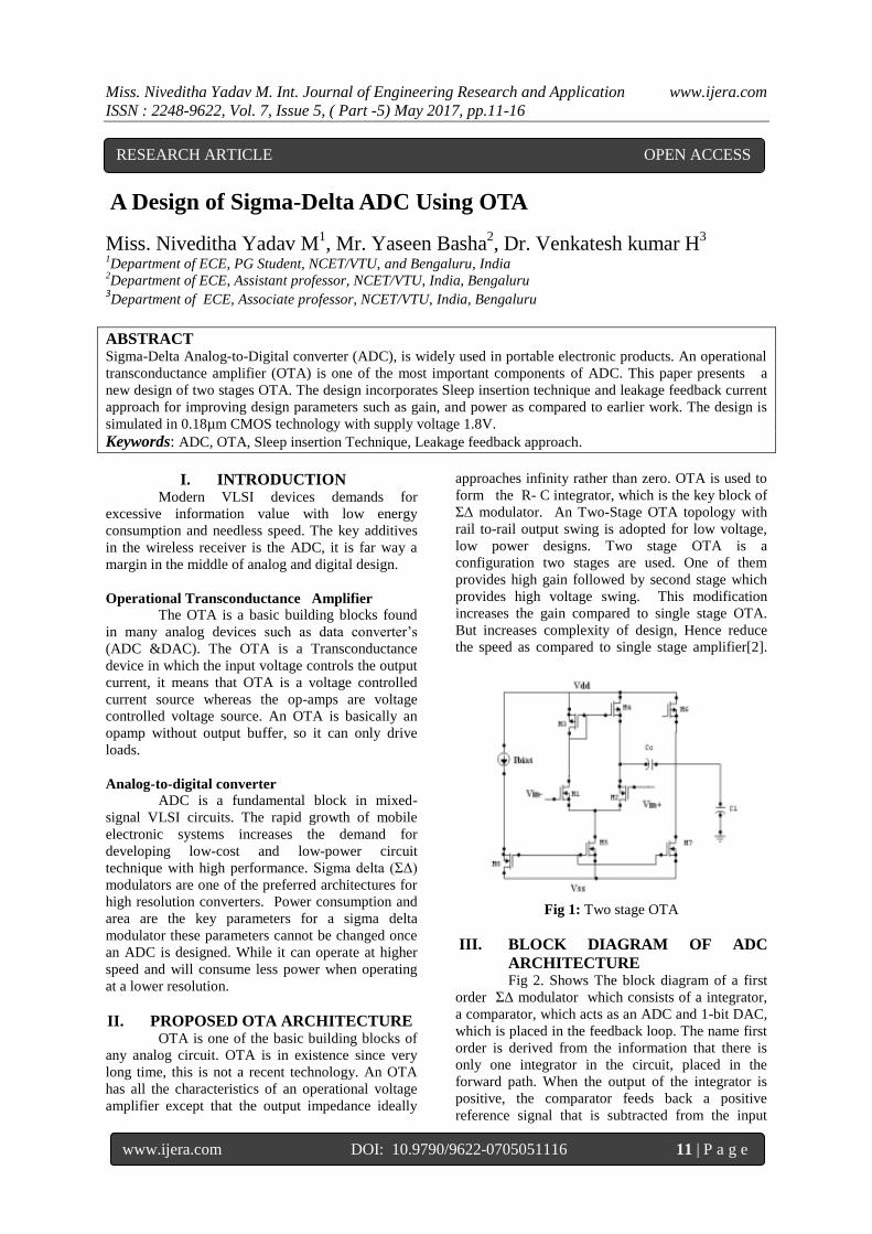
II. PROPOSED OTA ARCHITECTURE OTA is one of the basic building blocks of
any analog circuit. OTA is in existence since very
long time, this is not a recent technology. An OTA
has all the characteristics of an operational voltage
amplifier except that the output impedance ideally
approaches infinity rather than zero. OTA is used to
form the R- C integrator, which is the key block of
ΣΔ modulator. An Two-Stage OTA topology with
rail to-rail output swing is adopted for low voltage,
low power designs. Two stage OTA is a
configuration two stages are used. One of them
provides high gain followed by second stage which
provides high voltage swing. This modification
increases the gain compared to single stage OTA.
But increases complexity of design, Hence reduce
the speed as compared to single stage amplifier[2].
Fig 1: Two stage OTA
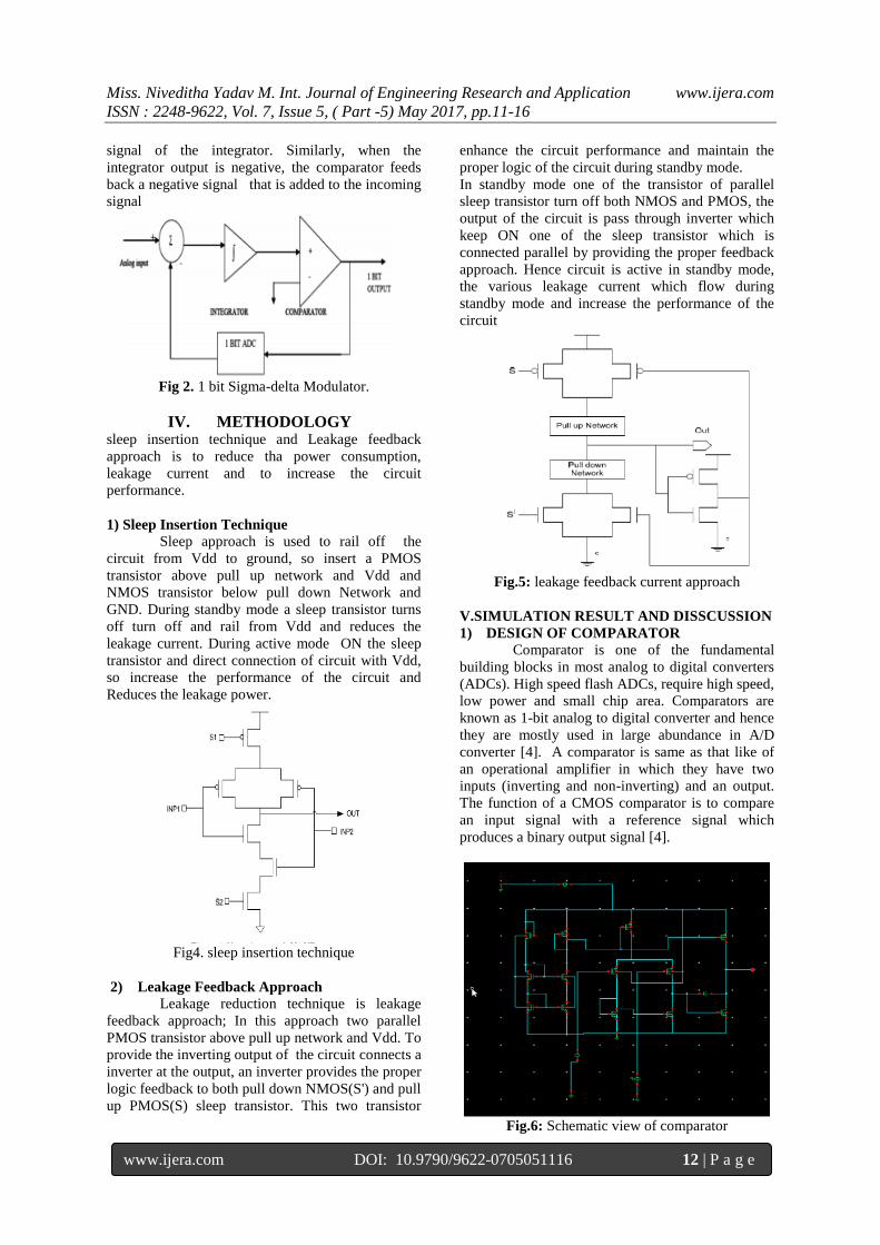
III. BLOCK DIAGRAM OF ADC
ARCHITECTURE Fig 2. Shows The block diagram of a first
order ΣΔ modulator which consists of a integrator,
a comparator, which acts as an ADC and 1-bit DAC,
which is placed in the feedback loop. The name first
order is derived from the information that there is
only one integrator in the circuit, placed in the
forward path. When the output of the integrator is
positive, the comparator feeds back a positive
reference signal that is subtracted from the input
RESEARCH ARTICLE OPEN ACCESS
Miss. Niveditha Yadav M. Int. Journal of Engineering Research and Application www.ijera.com
ISSN : 2248-9622, Vol. 7, Issue 5, ( Part -5) May 2017, pp.11-16
www.ijera.com DOI: 10.9790/9622-0705051116 12 | P a g e
signal of the integrator. Similarly, when the
integrator output is negative, the comparator feeds
back a negative signal that is added to the incoming
signal
Fig 2. 1 bit Sigma-delta Modulator.
IV. METHODOLOGY
sleep insertion technique and Leakage feedback
approach is to reduce tha power consumption,
leakage current and to increase the circuit
performance.
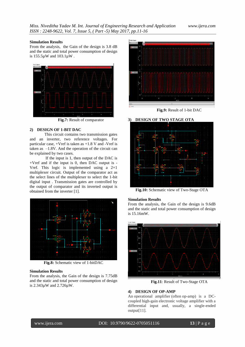
1) Sleep Insertion Technique
Sleep approach is used to rail off the
circuit from Vdd to ground, so insert a PMOS
transistor above pull up network and Vdd and
NMOS transistor below pull down Network and
GND. During standby mode a sleep transistor turns
off turn off and rail from Vdd and reduces the
leakage current. During active mode ON the sleep
transistor and direct connection of circuit with Vdd,
so increase the performance of the circuit and
Reduces the leakage power.
Fig4. sleep insertion technique
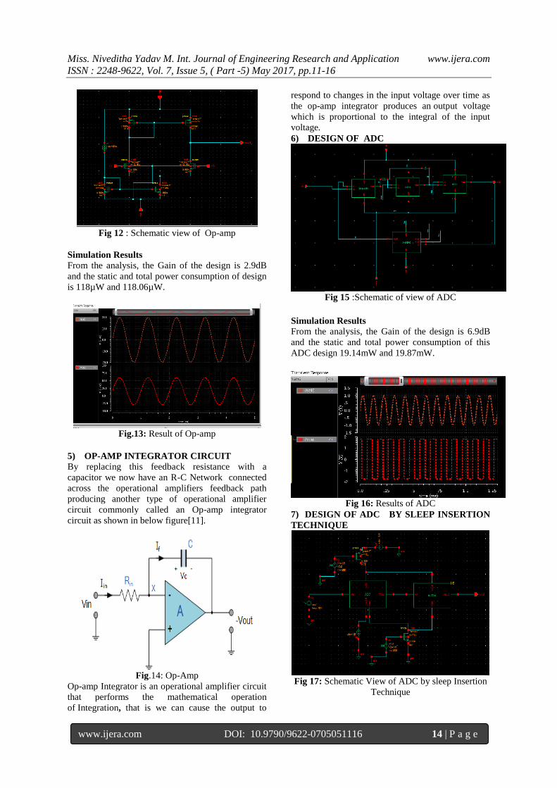
2) Leakage Feedback Approach Leakage reduction technique is leakage
feedback approach; In this approach two parallel
PMOS transistor above pull up network and Vdd. To
provide the inverting output of the circuit connects a
inverter at the output, an inverter provides the proper
logic feedback to both pull down NMOS(S') and pull
up PMOS(S) sleep transistor. This two transistor
enhance the circuit performance and maintain the
proper logic of the circuit during standby mode.
In standby mode one of the transistor of parallel
sleep transistor turn off both NMOS and PMOS, the
output of the circuit is pass through inverter which
keep ON one of the sleep transistor which is
connected parallel by providing the proper feedback
approach. Hence circuit is active in standby mode,
the various leakage current which flow during
standby mode and increase the performance of the
circuit
Fig.5: leakage feedback current approach
V.SIMULATION RESULT AND DISSCUSSION
1) DESIGN OF COMPARATOR
Comparator is one of the fundamental
building blocks in most analog to digital converters
(ADCs). High speed flash ADCs, require high speed,
low power and small chip area. Comparators are
known as 1-bit analog to digital converter and hence
they are mostly used in large abundance in A/D
converter [4]. A comparator is same as that like of
an operational amplifier in which they have two
inputs (inverting and non-inverting) and an output.
The function of a CMOS comparator is to compare
an input signal with a reference signal which
produces a binary output signal [4].
Fig.6: Schematic view of comparator
Miss. Niveditha Yadav M. Int. Journal of Engineering Research and Application www.ijera.com
ISSN : 2248-9622, Vol. 7, Issue 5, ( Part -5) May 2017, pp.11-16
www.ijera.com DOI: 10.9790/9622-0705051116 13 | P a g e
Simulation Results
From the analysis, the Gain of the design is 3.8 dB
and the static and total power consumption of design
is 155.5µW and 103.1µW .
Fig.7: Result of comparator
2) DESIGN OF 1-BIT DAC
This circuit contains two transmission gates
and an inverter, two reference voltages. For
particular case, +Vref is taken as +1.8 V and -Vref is
taken as –1.8V. And the operation of the circuit can
be explained by two cases.
If the input is 1, then output of the DAC is
+Vref and if the input is 0, then DAC output is -
Vref. This logic is implemented using a 2×1
multiplexer circuit. Output of the comparator act as
the select lines of the multiplexer to select the 1-bit
digital input . Transmission gates are controlled by
the output of comparator and its inverted output is
obtained from the inverter [1].
Fig.8: Schematic view of 1-bitDAC
Simulation Results
From the analysis, the Gain of the design is 7.75dB
and the static and total power consumption of design
is 2.343µW and 2.726µW.
Fig.9: Result of 1-bit DAC
3) DESIGN OF TWO STAGE OTA
Fig.10: Schematic view of Two-Stage OTA
Simulation Results
From the analysis, the Gain of the design is 9.6dB
and the static and total power consumption of design
is 15.16mW.
Fig.11: Result of Two-Stage OTA
4) DESIGN OF OP-AMP
An operational amplifier (often op-amp) is a DC-
coupled high-gain electronic voltage amplifier with a
differential input and, usually, a single-ended
output[11].
Miss. Niveditha Yadav M. Int. Journal of Engineering Research and Application www.ijera.com
ISSN : 2248-9622, Vol. 7, Issue 5, ( Part -5) May 2017, pp.11-16
www.ijera.com DOI: 10.9790/9622-0705051116 14 | P a g e
Fig 12 : Schematic view of Op-amp
Simulation Results
From the analysis, the Gain of the design is 2.9dB
and the static and total power consumption of design
is 118µW and 118.06µW.
Fig.13: Result of Op-amp
5) OP-AMP INTEGRATOR CIRCUIT
By replacing this feedback resistance with a
capacitor we now have an R-C Network connected
across the operational amplifiers feedback path
producing another type of operational amplifier
circuit commonly called an Op-amp integrator
circuit as shown in below figure[11].
Fig.14: Op-Amp
Op-amp Integrator is an operational amplifier circuit
that performs the mathematical operation
of Integration, that is we can cause the output to
respond to changes in the input voltage over time as
the op-amp integrator produces an output voltage
which is proportional to the integral of the input
voltage.
6) DESIGN OF ADC
Fig 15 :Schematic of view of ADC
Simulation Results
From the analysis, the Gain of the design is 6.9dB
and the static and total power consumption of this
ADC design 19.14mW and 19.87mW.
Fig 16: Results of ADC 7) DESIGN OF ADC BY SLEEP INSERTION
TECHNIQUE
Fig 17: Schematic View of ADC by sleep Insertion
Technique
Miss. Niveditha Yadav M. Int. Journal of Engineering Research and Application www.ijera.com
ISSN : 2248-9622, Vol. 7, Issue 5, ( Part -5) May 2017, pp.11-16
www.ijera.com DOI: 10.9790/9622-0705051116 15 | P a g e
Simulation Results
From the analysis, the Gain of the design is 6.9dB ,
and static and Total power consumed by OTA is
655.4µW .
Fig 18: Result of ADC by sleep Insertion
Technique
8) DESIGN OF ADC BY LEAKAGE
FEEDBACK APPROACH
Fig19: Schematic view of ADC by Leakage
Feedback Approach
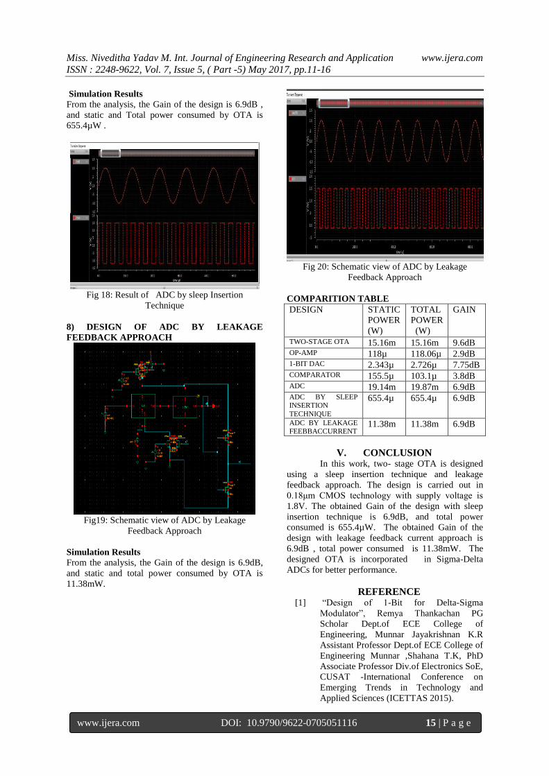
Simulation Results
From the analysis, the Gain of the design is 6.9dB,
and static and total power consumed by OTA is
11.38mW.
Fig 20: Schematic view of ADC by Leakage
Feedback Approach
COMPARITION TABLE
DESIGN STATIC
POWER
(W)
TOTAL
POWER
(W)
GAIN
TWO-STAGE OTA 15.16m 15.16m 9.6dB OP-AMP 118µ 118.06µ 2.9dB 1-BIT DAC 2.343µ 2.726µ 7.75dB COMPARATOR 155.5µ 103.1µ 3.8dB ADC 19.14m 19.87m 6.9dB ADC BY SLEEP INSERTION
TECHNIQUE
655.4µ 655.4µ 6.9dB
ADC BY LEAKAGE FEEBBACCURRENT
11.38m 11.38m 6.9dB
V. CONCLUSION
In this work, two- stage OTA is designed
using a sleep insertion technique and leakage
feedback approach. The design is carried out in
0.18μm CMOS technology with supply voltage is
1.8V. The obtained Gain of the design with sleep
insertion technique is 6.9dB, and total power
consumed is 655.4µW. The obtained Gain of the
design with leakage feedback current approach is
6.9dB , total power consumed is 11.38mW. The
designed OTA is incorporated in Sigma-Delta
ADCs for better performance.
REFERENCE
[1] “Design of 1-Bit for Delta-Sigma
Modulator”, Remya Thankachan PG
Scholar Dept.of ECE College of
Engineering, Munnar Jayakrishnan K.R
Assistant Professor Dept.of ECE College of
Engineering Munnar ,Shahana T.K, PhD
Associate Professor Div.of Electronics SoE,
CUSAT -International Conference on
Emerging Trends in Technology and
Applied Sciences (ICETTAS 2015).

Miss. Niveditha Yadav M. Int. Journal of Engineering Research and Application www.ijera.com
ISSN : 2248-9622, Vol. 7, Issue 5, ( Part -5) May 2017, pp.11-16
www.ijera.com DOI: 10.9790/9622-0705051116 16 | P a g e
[2] “Performance Evaluation of Different
Type of CMOS Operational
Transconductance Amplifier”, International
Journal of Science and Research (IJSR),
India Online ISSN: 2319-7064.
[3] [3] “Design, Simulation and Power
Analysis of Sigma-Delta Modulator using
0.18µm CMOS Technology”, Archana
Parutabadia*, Channakka L.a aDepartment
of Electronics & Communication
Engineering SDMCET Dharwad,India -
International Journal of Current
Engineering and Technology.
[4] “Design and Performance Analysis of a
Double-Tail Comparator for Low-Power
Applications”,IJSRET NOV-2014
[5] KushGulati and Hae-Seung Lee, “A High-
Swing, High-Performance CMOS
Telescopic Operational Amplifier”, IEEE
Journal of Solid-State Circuits, Vol. 33, No.
12, December 1998.
[6] R.Jacob Baker, Harry W. Li & David E.
Boyce, “CMOScircuit design, layout and
simulation”, IEEE Press Serieson
Microelectronic Systems, Prentice Hall of
IndiaPrivate Limited, 2004.
[7] Zahra Haddad Derafshi and Mohammad
HosseinZarifi, “Low-Power High-Speed
OTA in 0.35μm CMOS Process”, European
Journal of Scientific Research, ISSN 1450-
216X Vol.37 No.3 (2009), pp.368-375
[8] D.Nageshwarrao, S.VenkataChalamand,
V.MalleswaraRao, “Gain Boosted
Telescopic OTA with 110db Gain And
1.8GHz. UGF”, International Journal of
Electronic Engineering Research, ISSN
0975 - 6450 Volume 2 Number 2 (2010)
pp. 159 -166
[9] CarstenWulff, TrondYtterdal, “High Speed,
High Gain OTA in a Digital 90nmCMOS
Technology”, Department of Electronics
and Telecommunication, Norwegian
University of Science and Technology, N-
7491 Trondheim, Norway
[10] “Reduction of Leakage Power in CMOS
circuits (Gates) using Variable Body
Biasing with sleep insertion Technique”,1.
Sunita Yadav, M.Tech. Student of VLSI
Design Department, UTU Dehradun, UK
India, 2.Vishal Ramola, Assist. Prof. VLSI
Design Departmen[ [11] “Operational Amplifiers (Op Amps)”,
Professor Katherine Candler Notes courtesy
of Professor Sarah Harris.t, UTU,
Dehradun, UK India2
![ADC-20 und ADC-24 › download › datasheets › adc20...Datenlogger ADC-20 und ADC-24 ADC-20 ADC-24 Auflösung 20 Bit 24 Bit Anzahl Kanäle[1] 4 differenzial / 8 einpolig 8 differenzial](https://img.pdfslide.net/doc/110x75/5f23cbdc98bf2e58da663aad/adc-20-und-adc-24-a-download-a-datasheets-a-adc20-datenlogger-adc-20-und.jpg)