Embed Size (px)
Citation preview
1
Washington University in St. Louis
School of Engineering and Applied Science
Electrical and Systems Engineering Department
ESE498
Patch Antenna
By
Sana Naghipour
Supervisor Professor Spielman Professor Morely
Submitted in Partial Fulfillment of the Requirement for the BSEE Degree,
Electrical and Systems Engineering Department, School of Engineering and Applied Science, Washington University in St. Louis
May 2012

2
Abstract
The goal of this project is to design a patch antenna which would pick up cellphone
frequency. I preformed additional experiments to understand the antennas and their
characteristics, derived the theoretical equations, and used measuring equipment to
analyze the results. The prototype of the design was made first for a higher frequency which
leads to a smaller antenna and would fit in the board more accurate. Successions of
simulations have been proven to optimize the physical factors of the antenna for the
desired resonant frequency, bandwidth and input impedance. Then the cellphone
frequency was defined, and the design was developed based on that frequency. Some
adjustments were made to make the new design works with limitations. The results were
analyzed based on the gain, return losses, radiation pattern, and VSWR values, which are
the most significant characteristics of any antenna. The simulation analysis was executed
using the commercial antenna and network analyzer. The Microstrip patch antennas are
new, and are designed for higher frequencies. Patch antennaes have opened new doors to
new technology, and have replaced many previously designed antennas. This proposal has
been done to familiarize RF microwave designers with the design structure and
performance of the patch antenna. The designed antenna can be used in lab experiments in
which there is a need for an antenna which would capture certain frequencies of 842MHZ
or 2.105GHZ. The transmission and reflection coefficients should prove the accuracy and
good performance of the designed antenna. The more similar and more advanced design is
used in mobile antenna design, GPS navigation and network communication.

3
Acknowledgment
I wish to express my sincere gratitude to Professor Spielman for his guidance and
helpful feedbacks through the project process and providing me the required
equipment for this project.
I would also wish my special thanks to Professor Morely for providing me an
opportunity to do my design work on “The patch Antenna Design”.

4
• Table of Contents
1. Introduction
1.1 Problem statement
1.2 Literature review
1.3 Concept generation and reduction
2. Preview
2.1 S parameters and network analyzer
2.2 S parameters for 10dB coupler
3. Network analyzer calibration
4. Far field distance
5. Selection of the tool to measure the results
6. Orientation of the patch antenna
7. Dimension of the patch antenna for f=2.105GHz
8. Feed in method
9. Impedance matching
10. Analyzing the results of designed antenna (f=2.105GHz)
10.1 Gains of designed antenna for different angles
10.2 Beam width of designed antenna
11. Distinguish cellphone frequency
12. Dimensions of the designed patch antenna for f=842MHz
13. Adjustments of feed in method
14. Results
5
• List of Figures 1. Figure 1 : The incident and reflected power at each port 2. Figure 2 : The S parameters for two port system 3. Figure 3 : The ports and structure of 10dB coupler
4. Figure 4: The amplitude of S11 for 10dB coupler (In-Out Connection) 5. Figure 5 : The amplitude of S21 for 10dB coupler (In-Out Connection) 6. Figure 6 : The amplitude of S21 for 10dB coupler (In-Coupler Connection) 7. Figure 7 : The VSWR of 10dB couple 8. Figure 8 : The experiment set up for commercial antennas 9. Figure9 shows the S21 for two commercial antennas facing each other 10. Figure 10: The polarization pattern of the commercial antenna for f=1.5GHZ (In blue)
and f=2.0GHz(In red) 11. Figure 11: the polarization pattern of the commercial antenna for f=85MHz and
f=1.0GHz. 12. Figure 12: The structure of the designed patch antenna 13. Figure 13: The experiment set up of measuring the performance of designed patch
antenna using commercial antenna
14. Figure 14: S11 for f=2.105GHz when Y0=17mm 15. Figure 15: The polarization of designed patch antenna for f=2.105GHz 16. Figure 16: the peak for cellphone frequency of 842MHz
17. Figure 17: The designed patch configuration
18. Graph18: The losses of 90 degree feed in connection 19. Graph19: The losses of 45 degree feed in connecion 20. Figure 20: The measurement set up of checking designed patch antenna for f=
842MHz by an IPhone 21. Figure 21: Peak frequency of 842MHz of designed patch frequency in commercial
antenna bandwidth 22. Figure 22: S11 for Y0= 50mm 23. Figure23: S11 for Y0=10mm
• List of Tables 24. Table1 : The type of calibration kits used for different antenna and connections
25. Table2 : The values of S21 at f=850MHz and 1.5MHz for 0-360 degree rotation
26. Table3: The beam width of commercial antenna at different frequencies

6
27. Table 4: S21 values (gain) for microstrip patch rotation around the commercial
antenna
1. Introduction 1.1 Problem statement
The problems of making this design are briefly mentioned here, and they will be
explained in more detail included with proper solutions in the paper. The first challenge
was to understand how to work with new equipment and how to analyze my data,
results and graphs. I have done three experiments of measuring and analyzing the S
parameters of 10dB, 30dB, and 705S coupler, and I only included the results for 10dB in
the report as introduction to my experiment. I have enclosed a preview in the
introduction which makes it easier for the reader of this article. The second challenge,
which is also considerable, in any test is the reliability and accuracy of the
measurements and results. There might be more errors in experiments of higher
frequencies so the calibration process is required for the better results. The third part
was the recognizing orientation of the antenna, which was done experimentally and by
reading. The fourth problem was finding the dimensions of the antenna, and the
instruction for this part was given by professor Spielman. For the specific cellphone
frequency experiment, the challenges were to measure the frequency of the cellphone.
The other challenge was to adjust the type of feed in since the antenna did not fit with
the board size. Trimming was another challenge because it took a long time to find the
correct and fixed results before the copper tape lost its stickiness. I have discussed all
the results with professor Spielman, and necessary adjustments were recommended.
1.2 Literature Review The best article that helped me for this design was given by professor Spielman. The
antenna theory by Balanis was other good source of the theory and explanation of the
electric and magnetic fields orientation of the antenna design. The article The
7
Fundamental of patch Antenna Design and Performance by Gary Breed gave me a good
understanding of the polarization pattern and some characteristics of antenna design.
Another article, Design of New Multi Standard Patch Antenna
GSM/PCS/UMTS/HIPERLAN for Mobile cellular phones by M. Ben Ahmed about the
rectangular patch design in mobile phones was a little helpful. Most of the articles
already have the same explanations, and many of them used the same type of design
with different shape and feed in. Rectangular shape with either direct inset feed or
coaxial Probe feed was recommended in most articles.
1.3 Concept Generation and Reduction
I started this with the guidance professor Spielman provided for me. There was a brief
written guideline available which gave me the general idea of what needs to be done, but I
had to understand the reason for each step. I also searched for the other possible solutions.
After I finished the design for 2.105MHz frequency, then we came to the idea of designing it
for cellphone frequency. Since I have seen articles that mentioned about new patch
antenna design and their applications such as GPS navigation, network communication, and
mobile devices, I found it interesting to have an experiment of designing a practical patch
antenna for cellphone frequency. I knew that the design might be larger compared to the
cellphone antenna and I might not be able to have it so advanced and small, but it was a
good practical experiment which can be improved by more advanced studying of
magnetism and antenna design.
2. Preview
2.1 S parameters and network analyzer
In order to understand the results and procedure of this project, there is a need for an
introduction that explains the operation of the network analyzer and the parameters of this
system.
8
The network analyzer is used to measure the S parameters (scattering parameters)
of a one -or two-port device. In the case of high frequency, the traditional network
characterization of impedance and admittance parameters would not be done by simple
open-short circuit measurement, and instead it will be done by S parameters. S parameters
are defined as the behavior of the port or input-output relation of the network by travelling
waves moving along the transmission line and reflected waves.
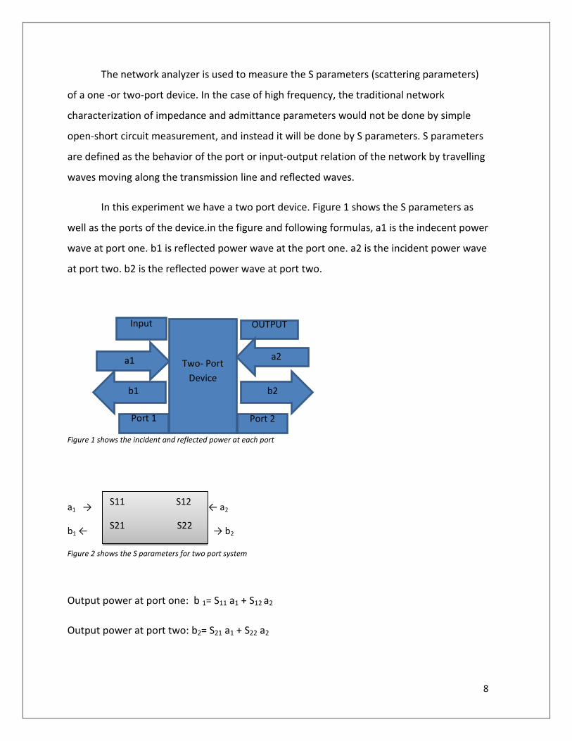
In this experiment we have a two port device. Figure 1 shows the S parameters as
well as the ports of the device.in the figure and following formulas, a1 is the indecent power
wave at port one. b1 is reflected power wave at the port one. a2 is the incident power wave
at port two. b2 is the reflected power wave at port two.
Figure 1 shows the incident and reflected power at each port
a1 → ← a2
b1 ← → b2
Figure 2 shows the S parameters for two port system
Output power at port one: b 1= S11 a1 + S12 a2
Output power at port two: b2= S21 a1 + S22 a2
Two- Port Device
a1
b1
Input OUTPUT
Port 1 Port 2
S11 S12
S21 S22
a2
b2

9
S11= |a2=0 =
In the S11parameter we are trying to find out how much input power is reflected at port
one. If there is no reflection, then S11 should be equal zero or be very small, which can be a
big negative number in dB. If all the power is being reflected, then S11 should be 1 or 0 dB.
S21= |a2=0 =
In this case, we are trying to find out how much input power at port one is being
transmitted to port two, or we are trying to find forward transmitted. S21 should be one or
0dB, If all the input power from port one is being transmitted. S21 should be 0 or -db, if none
or very small amount of input power is being transmitted to port two.
S22= |a1=0 =
In this case, we are estimating the amount of output reflected or we are trying to find out
how much input power at port two is being reflected at port two.
S12= |a1=0 =
The equation above is for the case of calculating the reverse transmission. In this case we
are trying to find out how much power from port two is being transmitted to port one.
S parameters at port one and two would be the same numbers or close. For example
S11=S22 and S12=S21. So for most of the experiments we only measure the values of
S11 and S21 since we are interested in checking the transmission.
The S parameters can be used to find the amount of reflection or transmission
power.
10
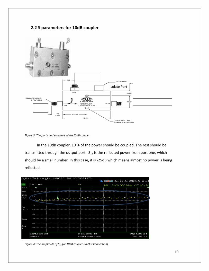
2.2 S parameters for 10dB coupler
Figure 3: The ports and structure of the10dB coupler
In the 10dB coupler, 10 % of the power should be coupled. The rest should be
transmitted through the output port. S11 is the reflected power from port one, which
should be a small number. In this case, it is -25dB which means almost no power is being
reflected.
Figure 4: The amplitude of S11 for 10dB coupler (In-Out Connection)
Isolate Port
Output/Transmission
Couple Port
Input
11
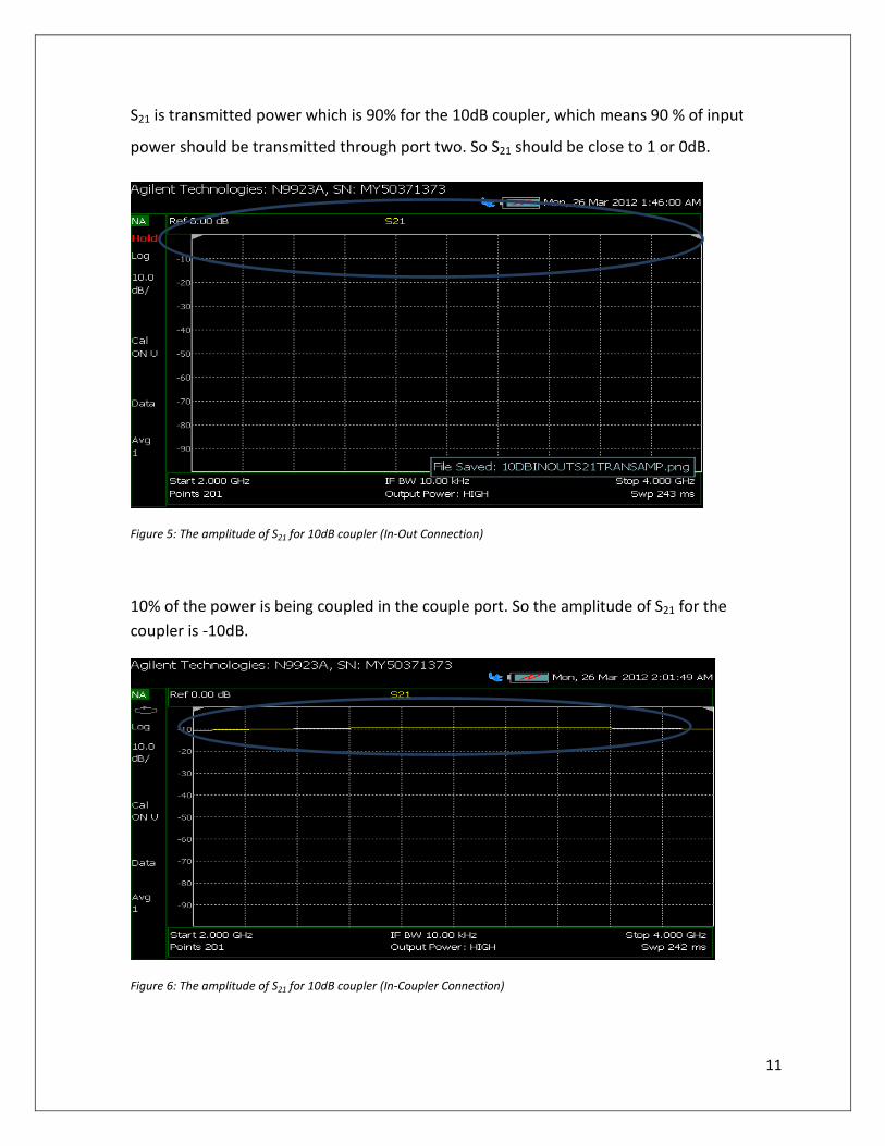
S21 is transmitted power which is 90% for the 10dB coupler, which means 90 % of input
power should be transmitted through port two. So S21 should be close to 1 or 0dB.
Figure 5: The amplitude of S21 for 10dB coupler (In-Out Connection)
10% of the power is being coupled in the couple port. So the amplitude of S21 for the coupler is -10dB.
Figure 6: The amplitude of S21 for 10dB coupler (In-Coupler Connection)
12
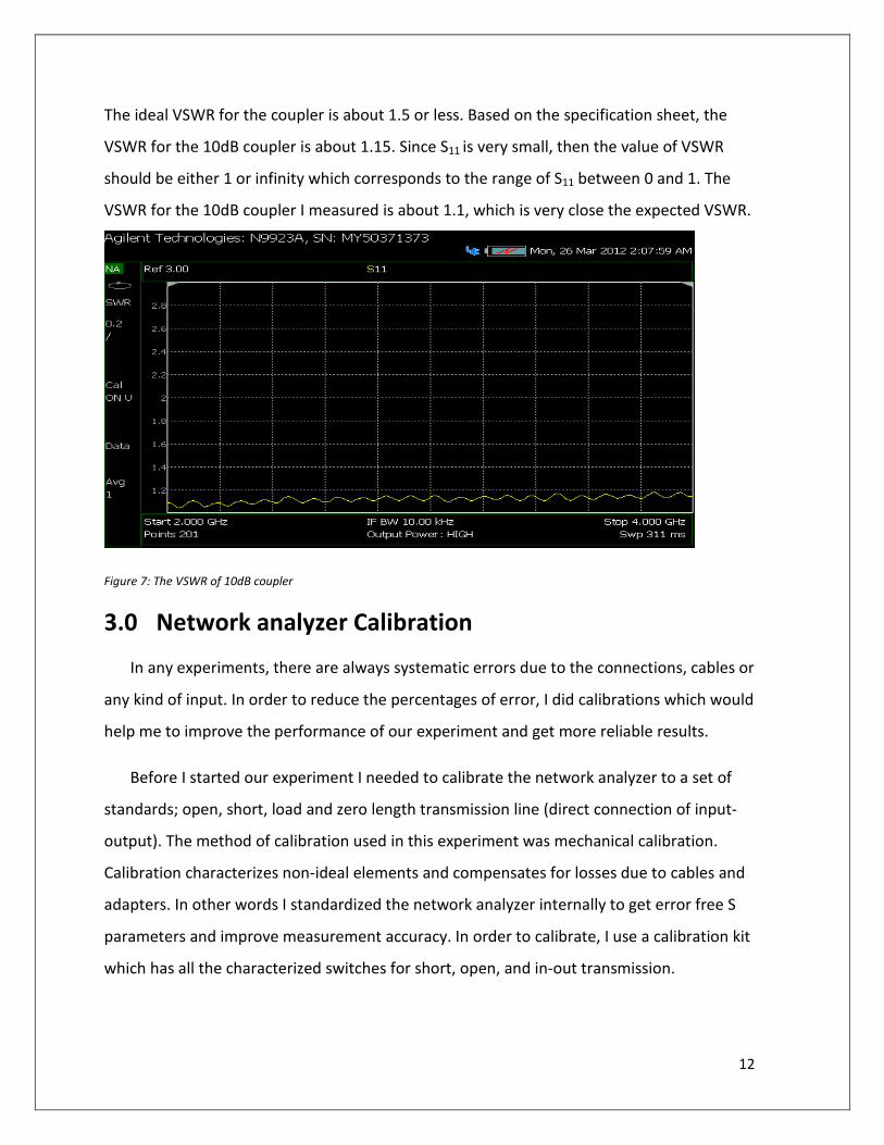
The ideal VSWR for the coupler is about 1.5 or less. Based on the specification sheet, the
VSWR for the 10dB coupler is about 1.15. Since S11 is very small, then the value of VSWR
should be either 1 or infinity which corresponds to the range of S11 between 0 and 1. The
VSWR for the 10dB coupler I measured is about 1.1, which is very close the expected VSWR.
Figure 7: The VSWR of 10dB coupler
3.0 Network analyzer Calibration
In any experiments, there are always systematic errors due to the connections, cables or
any kind of input. In order to reduce the percentages of error, I did calibrations which would
help me to improve the performance of our experiment and get more reliable results.
Before I started our experiment I needed to calibrate the network analyzer to a set of
standards; open, short, load and zero length transmission line (direct connection of input-
output). The method of calibration used in this experiment was mechanical calibration.
Calibration characterizes non-ideal elements and compensates for losses due to cables and
adapters. In other words I standardized the network analyzer internally to get error free S
parameters and improve measurement accuracy. In order to calibrate, I use a calibration kit
which has all the characterized switches for short, open, and in-out transmission.
13
Calibration can also fix any kind of systematic errors such as frequency, isolation between
signal paths, and mismatch between port impedance and leakage in the test set up.
At the beginning of the experiment I needed to calibrate the network to the
specific frequency range of the experiment. Calibration has to be done every
time cables or type of connections to the system change. Calibration also checks
the type of connections for us. In this case I used two port N type input
connections.
After finishing the calibration, I checked and measured the S parameters for
open, short, zero length transmission at each port to make sure calibration was
done correctly.
Table 1: The type of calibration kits used for different antenna and connections
Type of connection Type of calibration kit Commercial antenna T Shape 1250 Calibration kit NCM-NM-36-M02 Cable T Shape 1250 Calibration kit Patch Antenna 85033F Calibration kit SCA 52086-36 Cable 85033F Calibration kit
After the calibration was done, I analyzed the graphs for open circuit, short circuit,
load and direct connection at each port to make sure that calibration was done correctly.
The graphs of the experiment for port one which are available at appendix.
4.0 Far field distance:
The radiation pattern is different in different distances to the antenna. Far field or radiation field refers to the field pattern at larger distances. Antenna patterns usually are measured in the far field region. It’s important to choose the farthest distance based on the
dimensions of the antenna and wavelength. The formula for the distance is r = 2 . D is
largest dimension of the antenna which is W in this design.
For frequency of 842MHz, W= 125.912mm and the distance is r = 2 =8.89cm.
For the commercial antennas the distance is about 20cm.

14
5. Selection of the tool to measure the results
After finishing the experiment on the patch antenna I needed a type of
antenna that would be connected to the network analyzer to show the S21
parameters or the transmission from the designed antenna. The antenna that I
needed should have good band width and beam width to show all the parameters of
the designed antenna. Commercial antennas are known for having a broad
bandwidth, and I also did an experiment to check the performance of commercial
antennas.
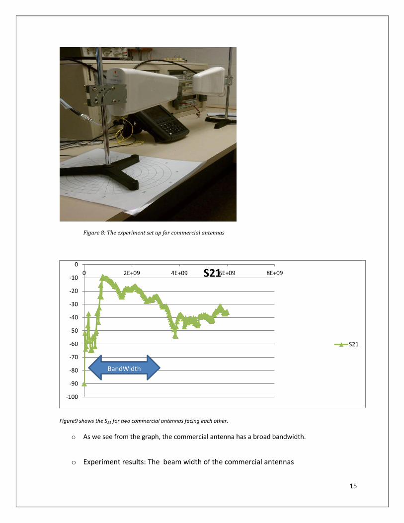
o Experiment Setup
For this part I calibrated the network analyzer for the frequency range of
2MHz-6GHz. The type of cables is CNM-NM-36-M02/X. Two commercial antennas
were attached to a pole with the height of 35 cm from the counter. Each antenna
was connected to the ports of the network analyzer. Antennas were separated 20
cm apart, and this distance was fixed for the entire experiment. 20 cm is the
distance of far field for the antenna, which was in the orientation of the antenna.
Antenna number one is connected to the left port of the network analyzer, and
antenna number two is connected to the second port of the network analyzer on the
right.
15
Figure 8: The experiment set up for commercial antennas
Figure9 shows the S21 for two commercial antennas facing each other.
o As we see from the graph, the commercial antenna has a broad bandwidth.
o Experiment results: The beam width of the commercial antennas
-100
-90
-80
-70
-60
-50
-40
-30
-20
-10
0 0 2E+09 4E+09 6E+09 8E+09 S21
S21
BandWidth

16
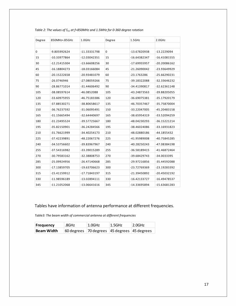
First, I set both antennas facing each other (0 degrees) and began rotating the antenna
connected to port 1 counter clockwise from 0 to 360 degrees, incrementing by 15 degrees.
While doing this, I measured and saved S21 values as .S2p files. After I took the
measurements, I graphed values of S21 at different frequencies. I chose frequencies of
.85GHz, 1.0GHz, 1.5GHz, 2.0GHz because they were evenly spaced in the frequency range of
the antenna specification, 800-2500MHz. Then I graphed the gains at different frequencies
and angles. The beam width varied for different frequencies. At 850MHz, the -3dB points
were approximately 30 degrees and -35 degrees, which add up to a bandwidth of 65
degrees. At 1GHz, the -3dB points are 30 degrees, and -30 degrees for a bandwidth of 60
degrees. At 1.5 GHz, the -3dB points are 15 degrees and -30 degrees, for a beam width of
45 degrees. Finally, at 2.0 GHz, the -3 dB points are 20 degrees and -25 degrees, for a beam
width of 45 degrees. These numbers show that the beam width is not the same for
different frequencies.
17
Table 2: The values of S21 at f=850MHz and 1.5MHz for 0-360 degree rotation
Tables have information of antenna performance at different frequencies.
Table3: The beam width of commercial antenna at different frequencies
Degree 850MHz=.85GHz 1.0GHz Degree 1.5GHz 2.0GHz
0 -9.805992624 -11.33331798 0 -13.67820938 -13.2229094
15 -10.33977864 -12.03042351 15 -16.64382347 -16.41081555
30 -12.21415304 -13.66608256 30 -17.69955957 -20.20086162
45 -16.18804273 -18.03166084 45 -21.26090042 -23.93649929
60 -20.15222658 -20.93481079 60 -23.1763286 -25.66290231
75 -26.0746946 -27.08059266 75 -39.18322088 -32.33646232
90 -28.86771014 -31.44606492 90 -34.41390817 -32.62361148
105 -38.08597614 -46.0852088 105 -43.24873563 -39.88205055
120 -33.60975955 -46.75183386 120 -36.69075381 -35.17920179
135 -37.88530271 -38.80658617 135 -46.70357467 -35.75870004
150 -36.76237592 -31.06095491 150 -33.22047005 -45.20483158
165 -31.15665494 -32.64440697 165 -38.65954319 -33.52094259
180 -31.23495524 -39.57725667 180 -48.04230293 -36.15221214
195 -35.82150901 -36.24284566 195 -38.46024086 -33.16931823
210 -31.76621999 -34.40254173 210 -48.02880186 -44.1855432
225 -37.42239891 -48.22067276 225 -41.95989008 -40.75845285
240 -34.53756602 -39.83967967 240 -40.28250243 -47.08384198
255 -37.54316982 -33.39015289 255 -36.58189415 -41.46872464
270 -30.79583162 -32.38808753 270 -39.68429743 -34.0033395
285 -25.09924956 -26.47140668 285 -29.97216856 -35.44592088
300 -17.13859705 -19.63706623 300 -23.72769369 -23.19283392
315 -15.41159912 -17.71843197 315 -21.39450892 -20.45032192
330 -11.98596189 -13.02894111 330 -16.42133727 -16.49478537
345 -11.21052068 -13.06641616 345 -14.33695894 -15.63681283
Frequency .8GHz 1.0GHz 1.5GHz 2.0GHzBeam Width 60 degrees 70 degrees 45 degrees 45 degrees
18
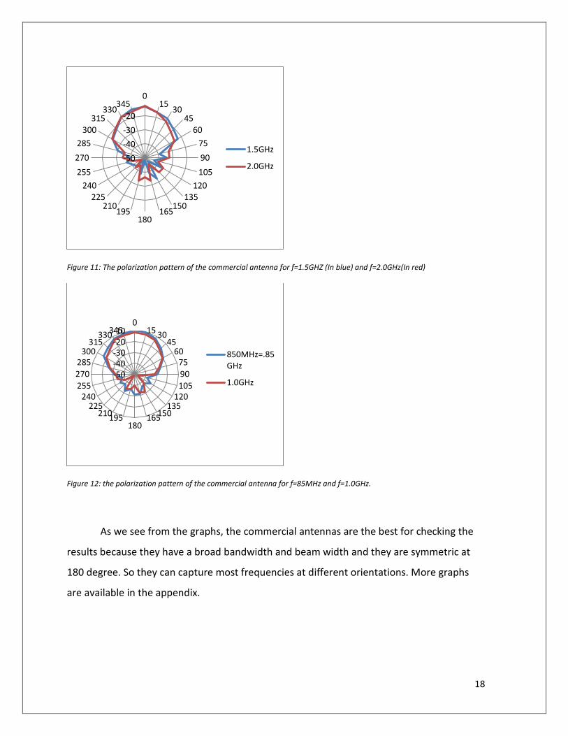
Figure 11: The polarization pattern of the commercial antenna for f=1.5GHZ (In blue) and f=2.0GHz(In red)
Figure 12: the polarization pattern of the commercial antenna for f=85MHz and f=1.0GHz.
As we see from the graphs, the commercial antennas are the best for checking the
results because they have a broad bandwidth and beam width and they are symmetric at
180 degree. So they can capture most frequencies at different orientations. More graphs
are available in the appendix.
-50
-40
-30
-20
0 15
30 45
60
75
90
105
120 135
150 165
180 195
210 225
240
255
270
285
300 315
330 345
1.5GHz
2.0GHz
-50 -40 -30 -20 -10
0 15 30
45 60
75 90 105
120 135
150 165 180
195 210 225
240 255 270 285
300 315
330 345
850MHz=.85GHz
1.0GHz
19
6. Orientation of the antenna:
The patch antenna is an array of two radiating narrow slots, each of width w and
height h, separated by a distance L. The open edges of the patch antenna behaves like wire
dipole antenna. The only difference is that their electric (E) and magnetic (H) fields due to
slots are reversed compared to the E and H of the wire dipole.
There is a magnetic current density around the side of the patch radiating into free space.
The microstrip antenna can be represented as two radiating slots along the length of the
patch with width W and height h. The slots are separated by the very low impedance of L
which acts like a transformer, and its length is ƛ /2. Maximum radiation is in the direction
perpendicular to the ground plane or normal to the path. Both slots, radiating the same
fields with magnetic current density M, have the same magnitude and phase along the
slots. The other two slots have the same current density. Their current density on each slot
has the same magnitude but opposite direction so the radiated electric and magnetic fields
will cancel each other out, so those two slots are called non- radiating slots. When we
measure the gain of the designed antenna, both antennas (transmitter and receiver) should
be in the position that their electric fields are parallel to have the maximum power
transmitted.
7. Dimensions of the patch antenna
The dimensions of the antenna, length and width are based on the resonant
frequency Due to the fringing of electric fields; we have to consider other parameters in the
calculations. In the other type of antennas, the length should be half the wavelength, which
is close in this case and there are other factors added because of dealing with two dielectric
constants of air and substrate. The board was available so I had no option of changing the
dielectric contestant or other characteristics of board. I calculated the dimension of the
patch antenna, and the patch was already made. In general the patch antenna is made of
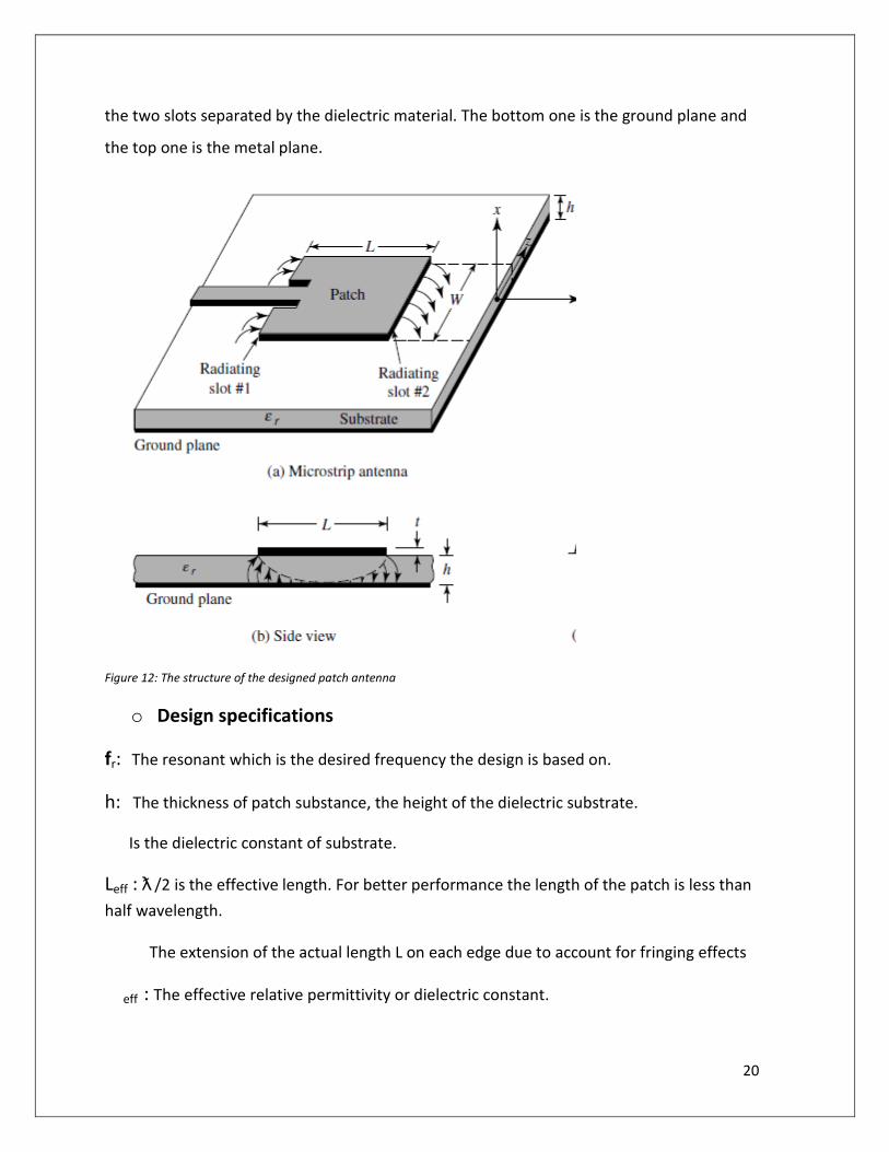
20
the two slots separated by the dielectric material. The bottom one is the ground plane and
the top one is the metal plane.
Figure 12: The structure of the designed patch antenna
o Design specifications
fr: The resonant which is the desired frequency the design is based on.
h: The thickness of patch substance, the height of the dielectric substrate.
Is the dielectric constant of substrate.
Leff : ƛ /2 is the effective length. For better performance the length of the patch is less than
half wavelength.
The extension of the actual length L on each edge due to account for fringing effects
eff : The effective relative permittivity or dielectric constant.
21
L: The physical length of the patch.
fr= 2.105GHz= 2.105E9 Hz
μ0 = 4π×10−7 N·A−2 ≈ 1.2566370614...×10−6 N·A−
0= 8.85… × 10−12
h = 0.062inch=0.0015748m
= 3.0 F/m
C= 3E8
W0=1mm
o Design calculations
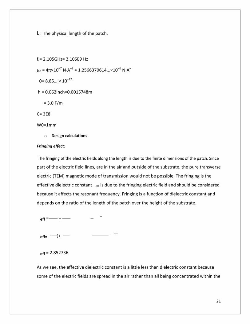
Fringing effect:
The fringing of the electric fields along the length is due to the finite dimensions of the patch. Since
part of the electric field lines, are in the air and outside of the substrate, the pure transverse
electric (TEM) magnetic mode of transmission would not be possible. The fringing is the
effective dielectric constant eff is due to the fringing electric field and should be considered
because it affects the resonant frequency. Fringing is a function of dielectric constant and
depends on the ratio of the length of the patch over the height of the substrate.
eff = +
eff= )+
eff = 2.852736
As we see, the effective dielectric constant is a little less than dielectric constant because
some of the electric fields are spread in the air rather than all being concentrated within the
22
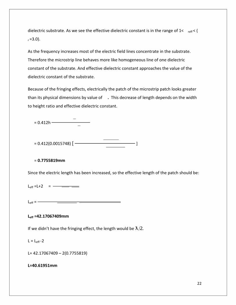
dielectric substrate. As we see the effective dielectric constant is in the range of 1< reff < (
r =3.0).
As the frequency increases most of the electric field lines concentrate in the substrate.
Therefore the microstrip line behaves more like homogeneous line of one dielectric
constant of the substrate. And effective dielectric constant approaches the value of the
dielectric constant of the substrate.
Because of the fringing effects, electrically the patch of the microstrip patch looks greater
than its physical dimensions by value of . This decrease of length depends on the width
to height ratio and effective dielectric constant.
= 0.412h
= 0.412(0.0015748) [ ]
= 0.7755819mm
Since the electric length has been increased, so the effective length of the patch should be:
Leff =L+2 =
Leff =
Leff =42.17067409mm
If we didn’t have the fringing effect, the length would be ƛ/2.
L = Leff -2
L= 42.17067409 – 2(0.7755819)
L=40.61951mm
23
The width W of the patch controls the input impedance and also increase the bandwidth. By
increasing the width, the impedance can be reduced. Values of μ0 = 4π×10−7 N·A−2 ≈
1.2566370614...×10−6 N·A−, 0= 8.85… × 10−12 are the free space characteristics.
W=
W=
W=50.36471mm
ƛ =
ƛ=
ƛ =0.08437977m
8. Feed in method
This type of feed in requires the direct connection of the smaller width
conducting strip to the edge of the microstrip patch. The benefit of this type of
connection is that the feed can be fixed on the same substrate to provide a planar
configuration, and this type of feeding is easy to fabricate, easy to design and
impedance matching. Also it would be the best choice that fit with my board
without reshaping the board.
24
9. Impedance matching
Since the impedance of the feed in and the patch are not the same, there will
be a lot of return losses. To decrease the power reflected, I used the method of
impedance matching.
The inset cutting in the patch is essential for impedance matching of the feed line to
the patch. In this experiment, I made a short circuit by cutting a narrow strip of 1mm
width and half-length long close to feed in. Then I changed the amount of that short
circuit by putting a slide of copper tape on cuts at the top of the antenna patch
where the cuts were and then keep trimming toward the center till I get close to the
desired frequency. By doing this I will increase the impedance of the patch in the
middle so the impedance of the feed in won’t be larger than the impedance of the
patch in the middle.Y0 is the amount of the length of the trimmed copper
slide.When Y0 is zero which is the edge of the slot, voltage is maximum and current
is minimum so the impedance is maximum. The minimum value of the impedance is
at the center of the patch where Y0= L/2. At that point the voltage is zero and the
current is maximum. The resonant input impedance decreases as the inset feed
moves from edges toward the center of the patch.
25
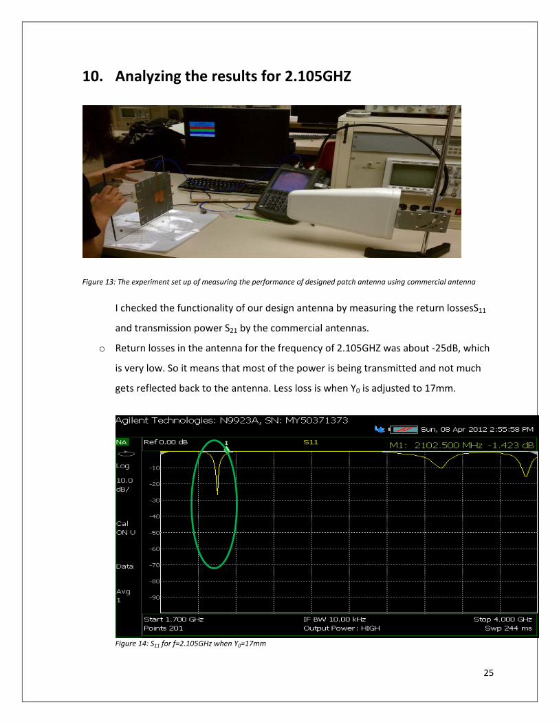
10. Analyzing the results for 2.105GHZ
Figure 13: The experiment set up of measuring the performance of designed patch antenna using commercial antenna
I checked the functionality of our design antenna by measuring the return lossesS11
and transmission power S21 by the commercial antennas.
o Return losses in the antenna for the frequency of 2.105GHZ was about -25dB, which
is very low. So it means that most of the power is being transmitted and not much
gets reflected back to the antenna. Less loss is when Y0 is adjusted to 17mm.
Figure 14: S11 for f=2.105GHz when Y0=17mm
26
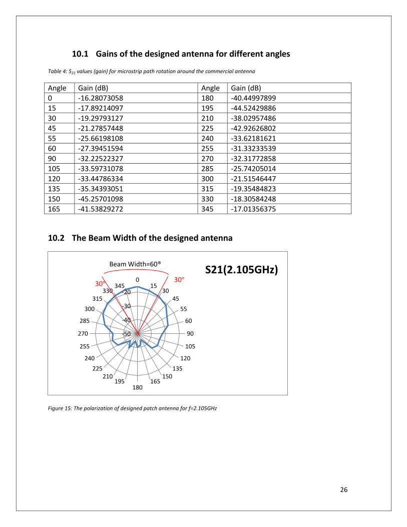
10.1 Gains of the designed antenna for different angles
Table 4: S21 values (gain) for microstrip path rotation around the commercial antenna
Angle Gain (dB) Angle Gain (dB) 0 -16.28073058 180 -40.44997899 15 -17.89214097 195 -44.52429886 30 -19.29793127 210 -38.02957486 45 -21.27857448 225 -42.92626802 55 -25.66198108 240 -33.62181621 60 -27.39451594 255 -31.33233539 90 -32.22522327 270 -32.31772858 105 -33.59731078 285 -25.74205014 120 -33.44786334 300 -21.51546447 135 -35.34393051 315 -19.35484823 150 -45.25701098 330 -18.30584248 165 -41.53829272 345 -17.01356375
10.2 The Beam Width of the designed antenna
Figure 15: The polarization of designed patch antenna for f=2.105GHz
-50
-40
-30
-20
0 15
30 45
55
60
90
105
120
135 150
165 180
195 210
225
240
255
270
285
300
315 330
345
S21(2.105GHz) 30° 30°
Beam Width=60®
27
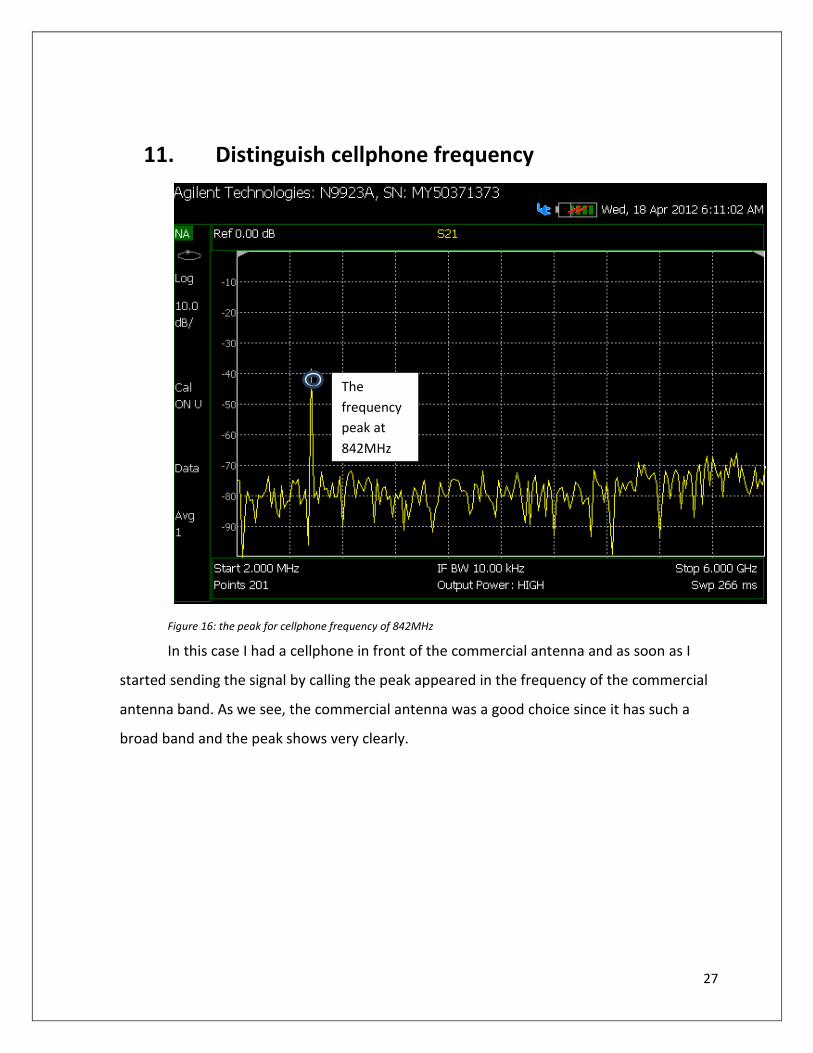
11. Distinguish cellphone frequency
Figure 16: the peak for cellphone frequency of 842MHz
In this case I had a cellphone in front of the commercial antenna and as soon as I
started sending the signal by calling the peak appeared in the frequency of the commercial
antenna band. As we see, the commercial antenna was a good choice since it has such a
broad band and the peak shows very clearly.
The frequency peak at 842MHz
28
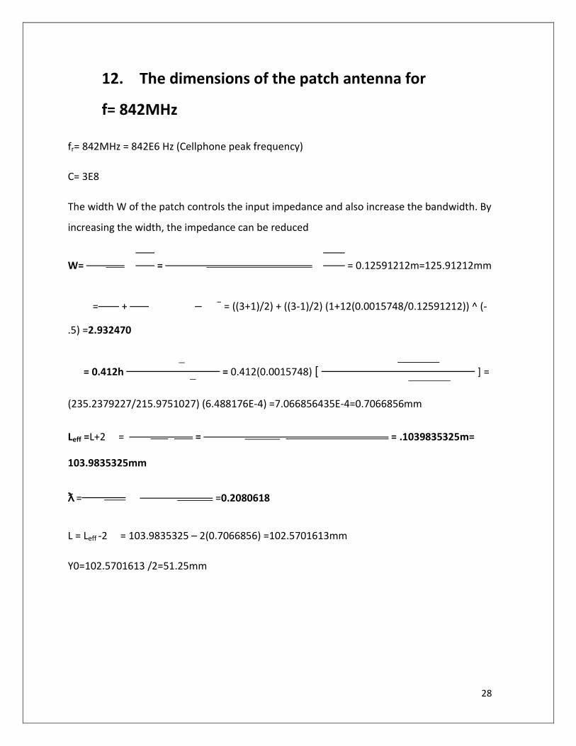
12. The dimensions of the patch antenna for
f= 842MHz
fr= 842MHz = 842E6 Hz (Cellphone peak frequency)
C= 3E8
The width W of the patch controls the input impedance and also increase the bandwidth. By
increasing the width, the impedance can be reduced
W= = = 0.12591212m=125.91212mm
= + = ((3+1)/2) + ((3-1)/2) (1+12(0.0015748/0.12591212)) ^ (-
.5) =2.932470
= 0.412h = 0.412(0.0015748) [ ] =
(235.2379227/215.9751027) (6.488176E-4) =7.066856435E-4=0.7066856mm
Leff =L+2 = = = .1039835325m=
103.9835325mm
ƛ = =0.2080618
L = Leff -2 = 103.9835325 – 2(0.7066856) =102.5701613mm
Y0=102.5701613 /2=51.25mm
29
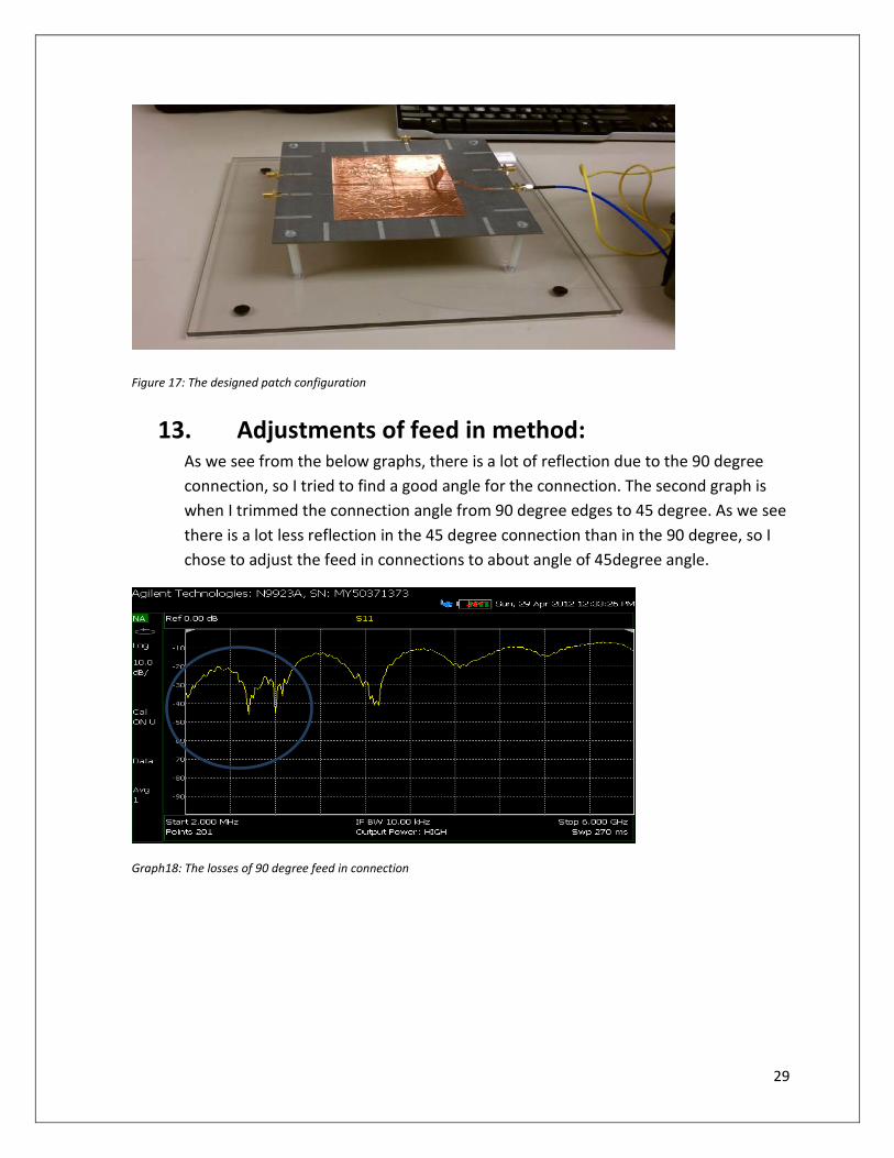
Figure 17: The designed patch configuration
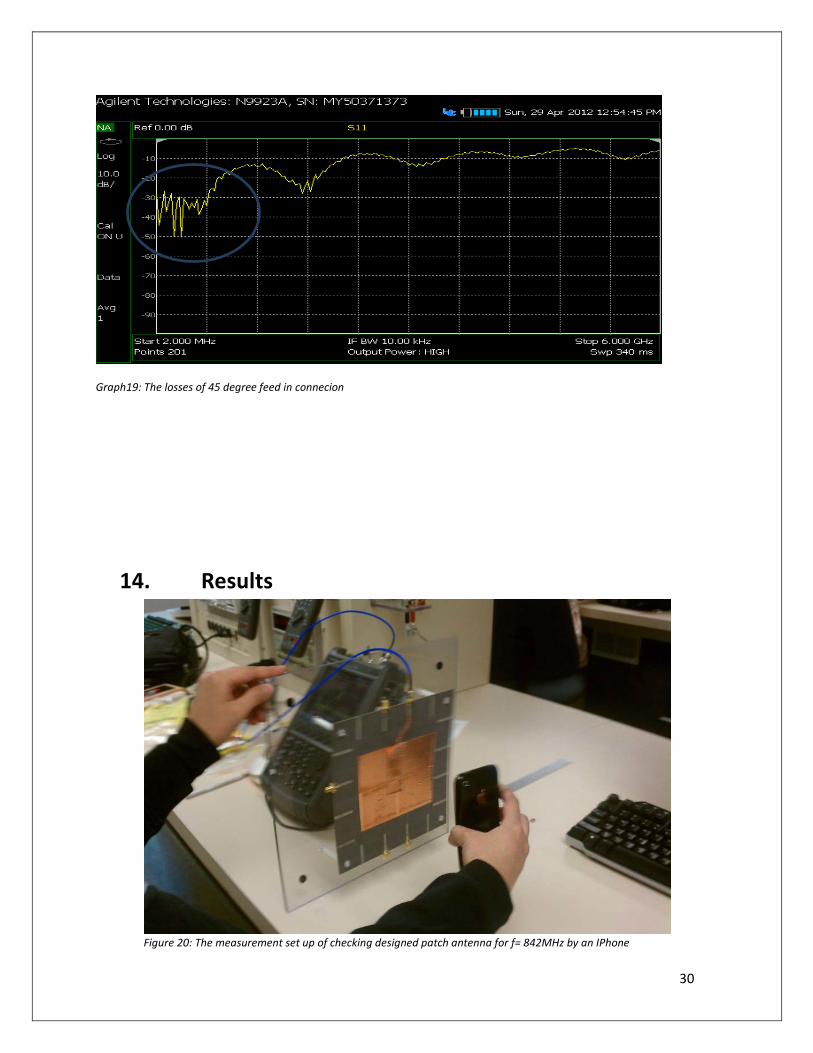
13. Adjustments of feed in method: As we see from the below graphs, there is a lot of reflection due to the 90 degree connection, so I tried to find a good angle for the connection. The second graph is when I trimmed the connection angle from 90 degree edges to 45 degree. As we see there is a lot less reflection in the 45 degree connection than in the 90 degree, so I chose to adjust the feed in connections to about angle of 45degree angle.
Graph18: The losses of 90 degree feed in connection
30
Graph19: The losses of 45 degree feed in connecion
14. Results
Figure 20: The measurement set up of checking designed patch antenna for f= 842MHz by an IPhone
31
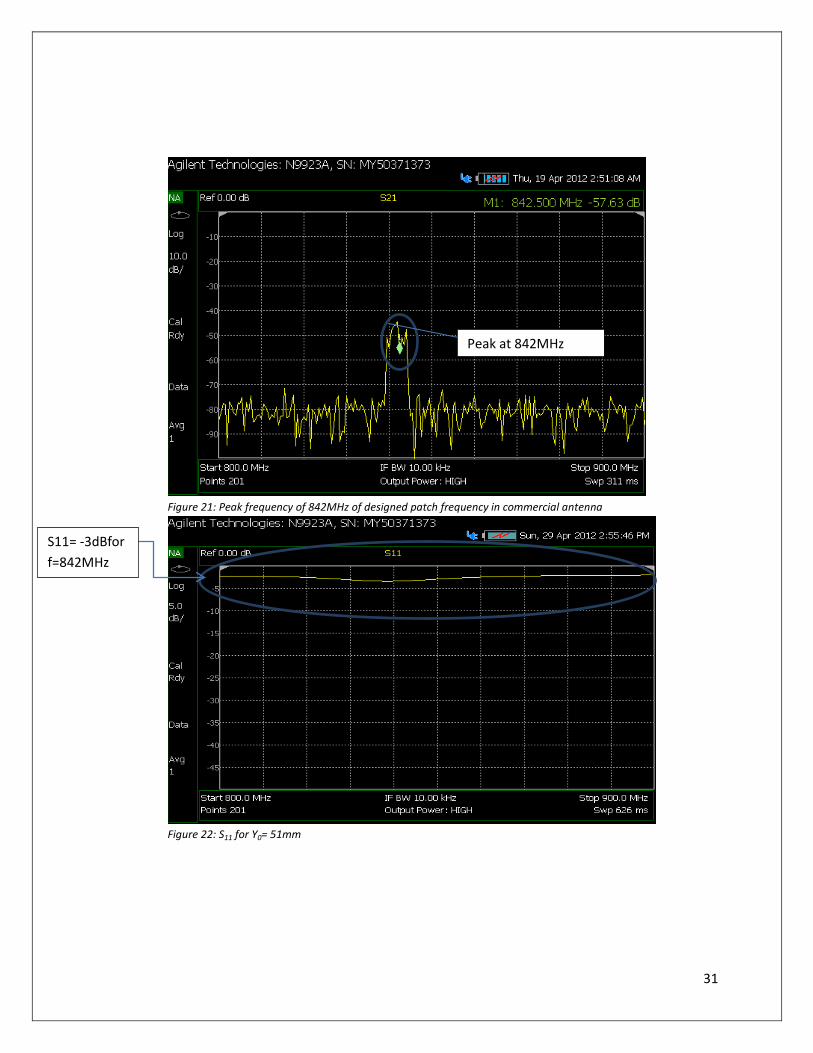
Figure 21: Peak frequency of 842MHz of designed patch frequency in commercial antenna
Figure 22: S11 for Y0= 51mm
S11= -3dBfor f=842MHz
Peak at 842MHz
32
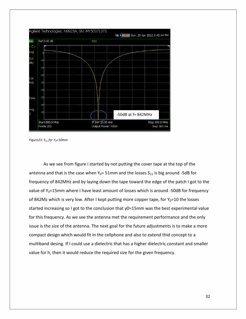
Figure23: S11 for Y0=10mm
As we see from figure I started by not putting the cover tape at the top of the
antenna and that is the case when Y0= 51mm and the losses S11 is big around -5dB for
frequency of 842MHz and by laying down the tape toward the edge of the patch I got to the
value of Y0=15mm where I have least amount of losses which is around -50dB for frequency
of 842Mz which is very low. After I kept putting more copper tape, for Y0=10 the losses
started increasing so I got to the conclusion that y0=15mm was the best experimental value
for this frequency. As we see the antenna met the requirement performance and the only
issue is the size of the antenna. The next goal for the future adjustments is to make a more
compact design which would fit in the cellphone and also to extend thid concept to a
multiband desing. If I could use a dielectric that has a higher dielectric constant and smaller
value for h, then it would reduce the required size for the given frequency.
-50dB at f= 842MHz
33
• Equipment & Costs:
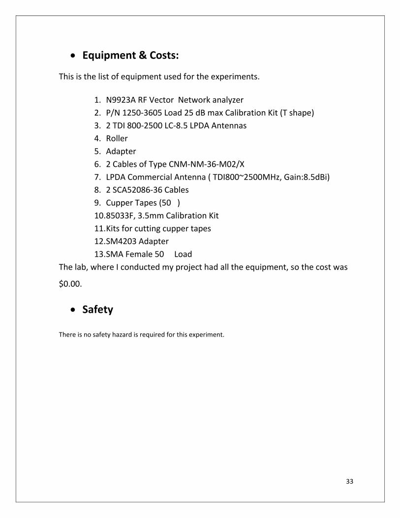
This is the list of equipment used for the experiments.
1. N9923A RF Vector Network analyzer 2. P/N 1250-3605 Load 25 dB max Calibration Kit (T shape) 3. 2 TDI 800-2500 LC-8.5 LPDA Antennas 4. Roller 5. Adapter 6. 2 Cables of Type CNM-NM-36-M02/X 7. LPDA Commercial Antenna ( TDI800~2500MHz, Gain:8.5dBi) 8. 2 SCA52086-36 Cables 9. Cupper Tapes (50 ) 10. 85033F, 3.5mm Calibration Kit 11. Kits for cutting cupper tapes 12. SM4203 Adapter 13. SMA Female 50 Load
The lab, where I conducted my project had all the equipment, so the cost was
$0.00.
• Safety
There is no safety hazard is required for this experiment.

34
• References:
(Breed, 2009)
(Balanis, 2005)
warehouse.cec.wustl.edu\home\links\sn10\winprofile\Desktop\cellphone antenna article.htm
http://highfrequencyelectronics.com/Archives/Mar09/HFE0309_Tutorial.pdf
http://classes.engineering.wustl.edu/ese331/331Project10.pdf