Embed Size (px)
Citation preview

Patterned Media Technology: Islands of Opportunity
Thomas R. Albrecht
Hitachi Global Storage TechnologiesSan Jose Research Center

2
Technology Roadmap: In Flux
2012
0.01
0.1
1
10
100
1000
10000
1980 1990 2000 2010
Are
al D
ensi
ty (G
b/sq
.in.)
100% / yr
30% / yr
60% / yrStandard FFMR headPRML channel Thin film disk
GMR head
DemosPerpendicular
Products
BPTAR?thermal instability regime
TAR?
BPMDTM?
3
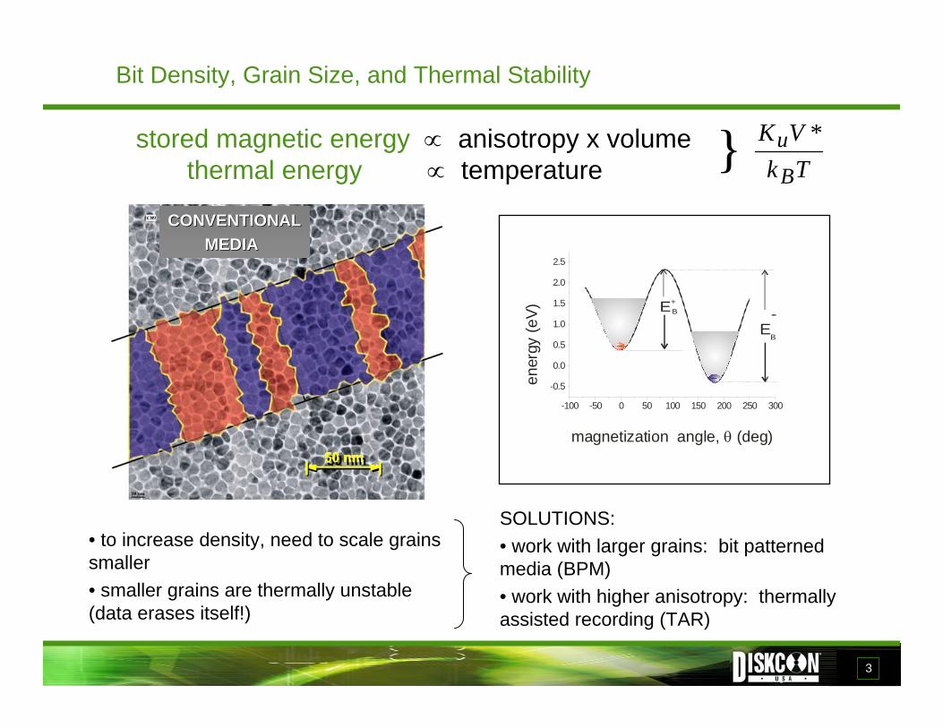
Bit Density, Grain Size, and Thermal Stability
50 nm50 nm
-100 -50 0 50 100 150 200 250 300
-0.5
0.0
0.5
1.0
1.5
2.0
2.5
ener
gy (e
V)
magnetization angle, (deg)θ
E-B
E+B
stored magnetic energy ∝ anisotropy x volumethermal energy ∝ temperature Tk
VK
B
u *}
• to increase density, need to scale grains smaller• smaller grains are thermally unstable (data erases itself!)
SOLUTIONS:• work with larger grains: bit patterned media (BPM)• work with higher anisotropy: thermally assisted recording (TAR)
CONVENTIONALCONVENTIONALMEDIAMEDIA
4
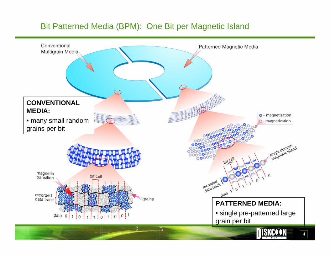
Bit Patterned Media (BPM): One Bit per Magnetic Island
PATTERNED MEDIA:• single pre-patterned large grain per bit
CONVENTIONAL MEDIA:• many small random grains per bit

5
Making BPM: The Semiconductor Industry Won’t Solve Our Problem
193 nm193 nm immersion with
water
DRAM ½ Pitch (nm)
2007 2010 2013 2016 2019
65
45
32
22
193 nm immersion with water193 nm immersion with other fluidsEUV, ML2
EUV193 nm immersion with other fluids & lenses193 nm with innovative immersion with waterImprint, ML2
EUVInnovative 193 nm immersion Imprint, ML2, Innovative Technology
16 Innovative Technology Innovative EUV, Imprint, ML2,
Research Required DevelopmentUnderway
QualificationProduction
ContinuousImprovement
FLASH
DRAM
The semiconductor industrywill not provide a lithography solution in time for patterned media
PATTERNED MEDIA
2005 ITRS Roadmap

6
Bit Patterned Media: Fabrication Overview
• Master pattern generation by rotary-stage e-beam lithography
• time consuming; features are ~20 nm diameter
• Low-cost pattern replication via nanoimprintlithography on each disk surface
• millions of replications
• Pattern transfer to substrate by reactive ion etching
• creates 1012 pillars on a substrate
• Blanket deposition of magnetic layer• material on tops of pillars forms isolated magnetic islands
e-Beam Lithography Master Mold Etching
UV-Cure Nanoimprinting
Disk Substrate Etching
Mag Layer Deposition

7
Master Pattern Generation Strategies
400 1600140012001000800600 20001800
rotary stage e-beam
e-beam + density multiplier
e-beam + self-assembly
Pattern density (Gbit/sq. inch)
J. Cheng et al. - MIT
TRACKSMASK SUPPORT LOCATION
SHADOW MASK
SUPPORT SPACER
shadow mask density multiplier
block copolymer self-assemblye-beam lithography
E. Dobisz, HGST
300 Gbit/in2

8
High Volume Pattern Replication via Nanoimprinting
• E-beam master will be expensive (many days to write one master pattern)
• Two generation nanoimprinting process envisioned for low-cost replication
• Very inexpensive: much cheaper than bit patterning used in solid-state storage
1 e-beam master10,000 replicananoimprint molds
100,000,000 imprinteddisk substrates

9
Nanoimprinting: Key Issues
Disk
Master
Replica mold• Fidelity of nano-scale features• Adhesion to substrate• Release from mold• Residual layer control• Rapid resist flow / elimination of air bubble trapping• Fast curing (oxygen inhibition, etc.)• Mold replication and mold lifetime• Resist etch resistance for pattern transfer• Scale-up to large areas + double-sided imprinting
substrate
nanoimprint resistresidual layerthickness
Successful imprint of ~50 nm period pillar features
• Patterned media may be one of the first large volume uses of nanoimprinting technology
• Relatively easy case: one “mask” and no overlay/alignment (unlike integrated circuits!)
T. Wu, M. Best - HGST

10
Magnetic Island Formation Approaches
B. Terris et al.
Prepatterned substrate
Magneticfilm
Isolated islands
Trench material
Unpatterned substrate
Magneticfilm
Isolated islands
Method 1: Prepatterned Substrate• clean, fast etching (RIE)
• Si, SiO2, Si3N4
• etch products volatile• “trench material” is present
• possible noise source• large topography (~40 nm)
• needs planarization
Method 2: Patterned Magnetic Film• dirty, slow etching (IBE)
• Co, Pd, Ni, etc.• redep of nonvolatile products
• island edge damage (ion bombardment)• no trench material• less topography
TEM cross sectionJ. Risner - HGST

11
Trench Noise
Cusp WAS
A. Moser, HGST
• 200 nm islands on 400 nm period (low density makes problem easy to see)
• DC erase (40 mA)
• Write one track (1250 fc/mm) (40 mA) – trench noise badly distorts readback
• DC erase with low write current (5 mA) – DC erases trench; islands unaffected
• Trench noise signal can be very large!

12
R/W Testing of BPM Disks (e-Beam Direct Write)
Spin Stand R/W Testing• well isolated islands at various densities• spin stand writing• no write synchronization or servo yet• both spin stand and MFM readback
100 Gbit/in2 (MFM readback)
100 Gbit/in2 (Spinstand readback)
Offs
et(u
m)
190 191 192 193 194 195 196 197 198
-0.2
0
0.2
50nm period, with sync mark
X. Wu, D. Kercher,
J. Risner, M. Best - HGST

13
Mag Layer Challenge: Switching Field Distribution
-12000 -10000 -8000 -6000 -4000 -2000
0.0
0.2
0.4
0.6
0.8
1.0
[Co(3.5)Pd(8.5)] x 8reference layer
4 16 65 180 300 500
Mic
ro-K
err s
igna
l [ar
b. u
nits
]
H [kOe]
( Gbit/in2)Pd (8.5Å)Co (3.5Å)
Co-Pd Multilayer Media: [Co(3.5)Pd(8.5)]x8 Pd(20)
Magnetic Force Microscopy 180 Gb/in2: Broad switching field distribution
Switching field distribution is broader than desired
Higher density (smaller islands) shows increased distribution width
Places challenging demands on write head field gradient
1000 Oe5000 Oe6000 Oe7000 Oe8000 Oe9000 Oe
M. Best - HGST
O. Hellwig - HGST
14
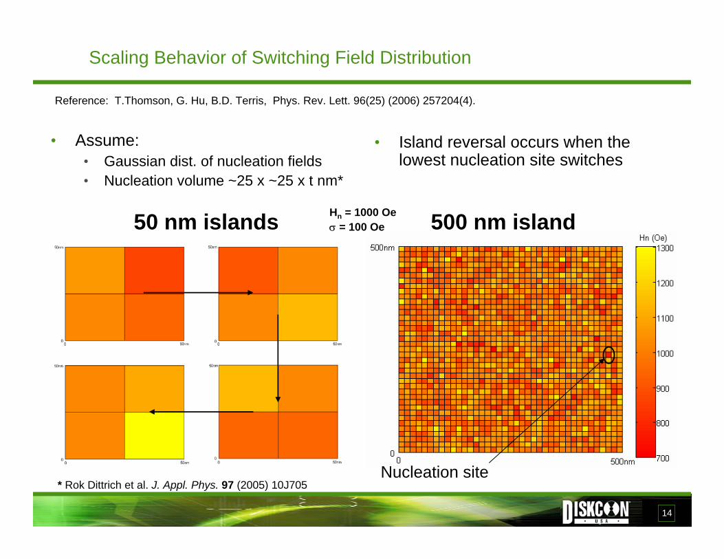
Scaling Behavior of Switching Field Distribution
• Assume: • Gaussian dist. of nucleation fields• Nucleation volume ~25 x ~25 x t nm*
50 nm islands 500 nm islandHn = 1000 Oeσ = 100 Oe
• Island reversal occurs when the lowest nucleation site switches
Nucleation site* Rok Dittrich et al. J. Appl. Phys. 97 (2005) 10J705
Reference: T.Thomson, G. Hu, B.D. Terris, Phys. Rev. Lett. 96(25) (2006) 257204(4).

15
Dipolar Contribution to Switching Field Distribution
• At higher density, dipolar fields (4πMs) become significant source of SFD• Can reduce by reducing Ms, but this leads to reduced readback signal
Hellwig et al, APL 90, 162516 (2007)

16
Write Synchronization
GMR read elementinductive writeelement
CONTINUOUS MEDIA
PATTERNED MEDIA
CONTINUOUS MEDIA:
Magnetic transitions can be written at arbitrary positions
Timing controlled by fixed clock
PATTERNED MEDIA:
Writing must be synchronized to passage of individual islands under head
Misaligned writing produces errors
System must sense phase and frequency of islands and synchronize write current switching
50 nm50 nm
17
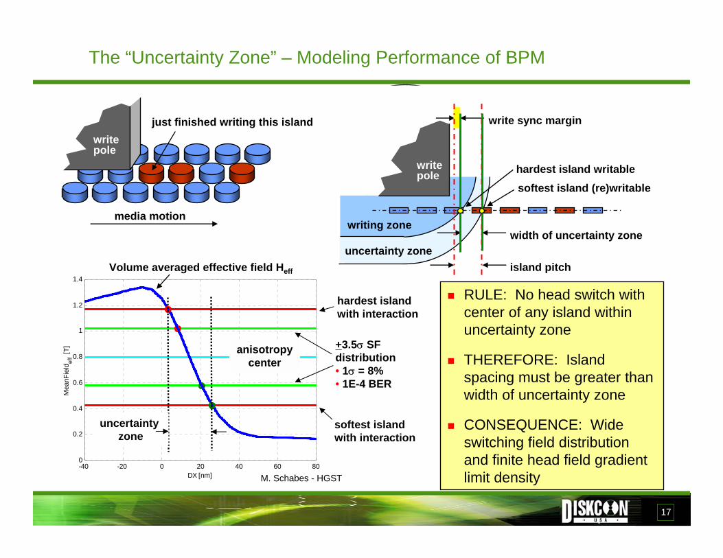
The “Uncertainty Zone” – Modeling Performance of BPM
writepole
width of uncertainty zone
island pitch
write sync margin
writing zone
uncertainty zone
hardest island writablesoftest island (re)writable
writepole
media motion
just finished writing this island
-40 -20 0 20 40 60 800
0.2
0.4
0.6
0.8
1
1.2
1.4
Mea
nFie
ldef
f [T]
DX [nm]
DY=0 nmVolume averaged effective field Heff
+3.5σ SFdistribution• 1σ = 8%• 1E-4 BER
hardest island with interaction
uncertainty zone
softest island with interaction
anisotropycenter
RULE: No head switch with center of any island within uncertainty zone
THEREFORE: Island spacing must be greater than width of uncertainty zone
CONSEQUENCE: Wide switching field distribution and finite head field gradient limit densityM. Schabes - HGST

18
Areal Density [Tb/in2] Design Charts for BPM
σprint=3 nm
σprint=2 nm
switching field distribution of the islands
gradient of the effective write field profile
Are
alD
ensi
ty [T
b/in
2 ]
areal density contours [Tb/in2]pooled fabrication tolerance
• centroid jitter• shape jitter
pooled synchronization tolerance• write synchronization jitter• NRO, etc.
BERw=10-6
K1=2.7x10⁵ J/m3
thermal stabilitycontours [K1V/kBT] at 300 K: need >40
disqualified region of parameter space due toreadback jitter or thermal stability
2 Tb/in2 design exampleσHsw=1400 Oegrad(Heff)=390 Oe/nmEb=110 kBT
realistic regime M. Schabes – HGSTTo be presented at PMRC 2007

19
BAR Effects – Tradeoffs with Fabrication and Sync Tolerances
BAR = 1: 4 Tb/in2
M. S
chab
es-H
GST
tighter tolerances
BAR = 2: 3 Tb/in2
BAR = 4: 1.6 Tb/in2 BAR = 4: 4 Tb/in2

20
Low BAR Write Field Penalty
• Write field scales poorly if BAR decreased compared to conventional (BAR) recording
• Solid angle modeling shows that reduced pole tip area caused by lowered BAR results in strongly reduced field
• Modeled geometry assumes a fixed pole width and thickness ratio of 2 and constant values for media and head to media dimensions
• Reduced write field attacks the very advantage that BPM is intended to achieve (thermal stability with good writability)
BAR reduced by 5: Area decrease by 86%
Same BARArea decrease by 29%
BAR reduced by 5: Field drop 58%
T. Olson - HGST
Same BARField drop 11%
Increase Areal density by 40 % Increase Areal density by 40 %

21
How Far Can BPM Go with Exchange Spring?
Use Co3Pt islands and (graded) exchange springs
M. Schabes - HGST
Limited by thermal stability at ~ 30 Tb/in2
Control over lateral coupling:Exchange spring more easily applied to BPM than conventional PMR

22
Pre-Patterned Servo
data tracks servo “sector” track ID Gray code
“quad burst”tracking pattern
track direction (circumferential)
Very precise servo features created along with data track islands
Eliminates need for separate servowriting operation Z. Bandic - HGST

23
Bit Patterned Media: Summary
• Thermal stability drives the need for BPM• Media fabrication looks feasible
• Master pattern generation by high resolution e-beam lithography• Pattern replication by UV-cure nanoimprint lithography• Etching of substrate or mag layer
• Achieving suitable magnetic properties is challenging• Island switching field distribution (limits recording density due to finite head
field gradient)• BPM is Extendible
• Thermal stability may be possible well beyond 10 Tb/in2 with exchange spring
• Integration of patterned media into a hard disk drive requires:• Write synchronization• Pre-patterned servo (reduces cost)
A. Moser - HGST