Embed Size (px)
Citation preview

www.apexanalog.com© Apex Microtechnology Inc
All rights reserved
Power Booster Amp
PB51 • PB51A
lifier RoHSCOMPLIANT
FEATURES
• Wide Supply Range – ±15V to ±150V• High Output Current –
1.5A Continuous (PB51), 2.0A Continuous (PB51A)
• Voltage and Current Gain• High Slew –
50V/µs Minimum (PB51)75V/µs Minimum (PB51A)
• Programmable Output Current Limit• High Power Bandwidth – 320 kHz Minimum• Low Quiescent Current – 12mA Typical• Evaluation Kit – EK29
APPLICATIONS
• High Voltage Instrumentation• Electrostatic Transducers & Deflection• Programmable Power Supplies up to 280V P-P
DESCRIPTION
The PB51 is a high voltage, high current amplifier designed to provide voltage and current gain for a smallsignal, general purpose op amp. Including the power booster within the feedback loop of the driver amplifierresults in a composite amplifier with the accuracy of the driver and the extended output voltage range andcurrent capability of the booster. The PB51 can also be used without a driver in some applications, requiringonly an external current limit resistor to function properly.
The output stage utilizes complementary MOSFETs, providing symmetrical output impedance and elimi-nating second breakdown limitations imposed by Bipolar Transistors. Internal feedback and gainset resistorsare provided for a pin-strapable gain of 3. Additional gain can be achieved with a single external resistor.Compensation is not required for most driver/gain configurations, but can be accomplished with a singleexternal capacitor. Enormous flexibility is provided through the choice of driver amplifier, current limit, sup-ply voltage, voltage gain, and compensation.
This hybrid circuit utilizes a beryllia (BeO) substrate, thick film resistors, ceramic capacitors and semicon-ductor chips to maximize reliability, minimize size and give top performance.
Ultrasonically bonded aluminum wires provide reliable interconnections at all operating temperatures.The 12-pin Power SIP is electrically isolated.
. Nov 2015PB51U Rev k

PB51 • PB51A
TYPICAL CONNECTION
Figure 1: Typical Connection
2 PB51U Rev k
PB51 • PB51A
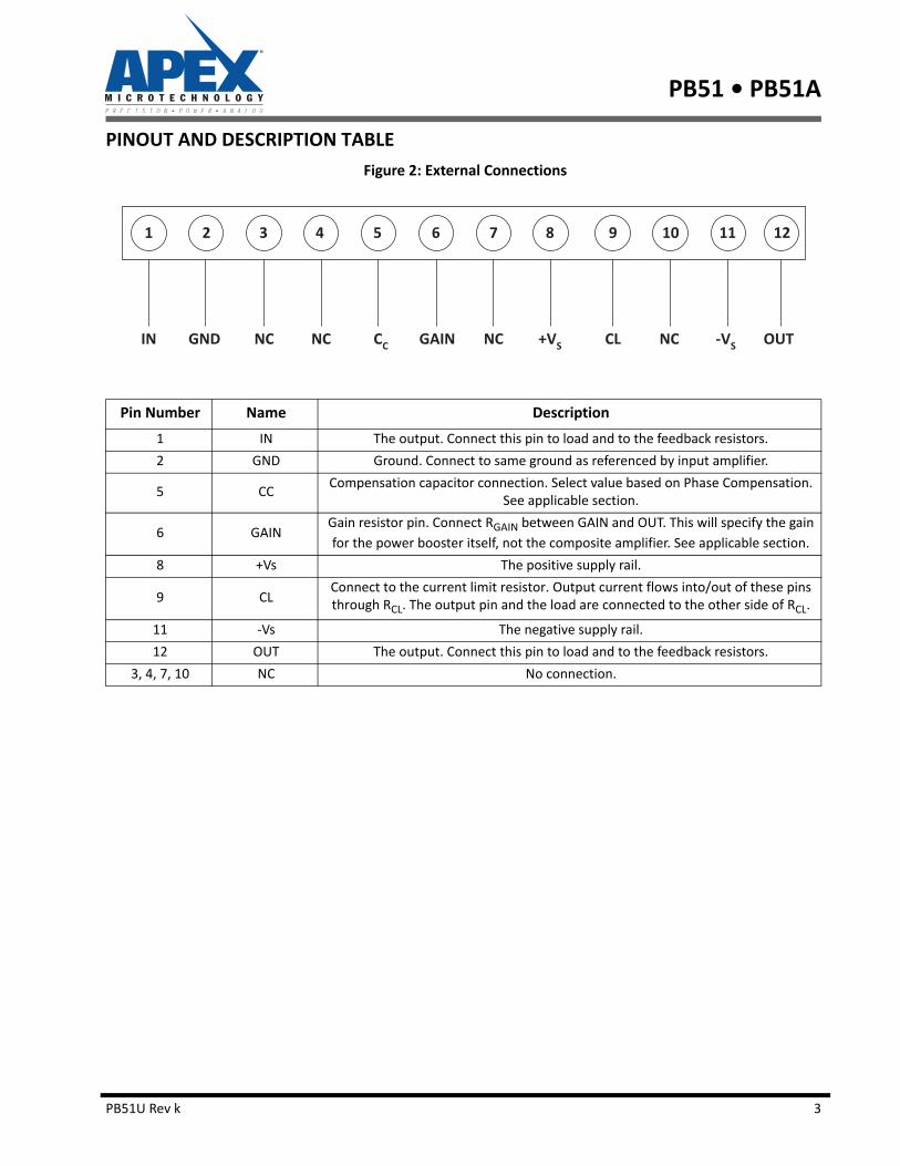
PINOUT AND DESCRIPTION TABLE
Figure 2: External Connections
Pin Number Name Description
1 IN The output. Connect this pin to load and to the feedback resistors.
2 GND Ground. Connect to same ground as referenced by input amplifier.
5 CCCompensation capacitor connection. Select value based on Phase Compensation.
See applicable section.
6 GAINGain resistor pin. Connect RGAIN between GAIN and OUT. This will specify the gain
for the power booster itself, not the composite amplifier. See applicable section.
8 +Vs The positive supply rail.
9 CLConnect to the current limit resistor. Output current flows into/out of these pins through RCL. The output pin and the load are connected to the other side of RCL.
11 -Vs The negative supply rail.
12 OUT The output. Connect this pin to load and to the feedback resistors.
3, 4, 7, 10 NC No connection.
PB51U Rev k 3

PB51 • PB51A
SPECIFICATIONS
The power supply voltage specified under typical (TYP) applies, TC = 25°C unless otherwise noted.
ABSOLUTE MAXIMUM RATINGS
The PB51 is constructed from MOSFET transistors. ESD handling procedures must be observed.The internal substrate contains beryllia (BeO). Do not break the seal. If accidentally broken, donot crush, machine, or subject to temperatures in excess of 850°C to avoid generating toxicfumes.
INPUT
Parameter Symbol Min Max Units
Supply Voltage, total +Vs to -Vs 300 V
Output Current, within SOA IO 2 A
Power Dissipation, internal @ Tc = 25°C1
1. Long term operation at the maximum junction temperature will result in reduced product life. Derate internal power dis-sipation to achieve high MTTF (Mean Time to Failure).
PD 83 W
Input Voltage, referred to COM VIN -15 15 V
Temperature, pin solder, 10s max. 260 °C
Temperature, junction 1 TJ 175 °C
Temperature Range, storage -55 +125 °C
Operating Temperature Range, case TC -40 +85 °C
ParameterTest
Conditions
PB51 PB51AUnits
Min Typ Max Min Typ Max
Offset Voltage, initial ±0.75 ±1.75 * ±1.0 V
Offset Voltage vs. Temperature Full temp range1
1. Guaranteed by design but not tested.
-4.5 -7 * * mV/°C
Input Impedance, DC 25 50 * * kΩ
Input Capacitance 3 * pF
Closed Loop Gain Range 3 10 25 * * * V/V
Gain Accuracy, internal Rg, Rf AV = 3 ±10 ±15 * * %
Gain Accuracy, external Rf AV = 10 ±15 ±25 * * %
Phase Shift
f=10 kHz, AVCL =
10, CC = 22pF10 * °
f =200 kHz, AVCL
= 10, CC = 22pF60 * °
CAUTION
4 PB51U Rev k

PB51 • PB51A
OUTPUT
POWER SUPPLY
ParameterTest
Conditions
PB51 PB51AUnits
Min Typ Max Min Typ Max
Voltage Swing IO = 1.5A (PB58),
2A (PB58A)±VS–11 ±VS–8 ±VS–15 ±VS–11 V
Voltage Swing IO = 1A ±VS–10 ±VS–7 * * V
Voltage Swing IO = 0.1A ±VS–8 ±VS–5 * * V
Current, continuous 1.5 2.0 A
Slew Rate Full temp range 50 100 75 * V/µs
Capacitive Load Full temp range 2200 * pF
Settling Time to 0.1% RL = 100, 2V step 2 * µs
Power Bandwidth VC = 100 VP-P 160 230 240 * kHz
Small Signal BandwidthCC=22pF, AV=25,
VCC = ±100100 * kHz
Small Signal BandwidthCC =22pF, AV=3,
VCC = ±301 * MHz
ParameterTest
Conditions
PB51 PB51AUnits
Min Typ Max Min Typ Max
Voltage, ±VS 1
1. +VS and –VS denote the positive and negative supply rail respectively.
Full temp range ±152
2. +VS/–VS must be at least 15V above/below COM.
±60 ±150 * * * V
Current, quiescent
VS = ±15
VS = ±60
VS = ±150
111214 18
*** *
mAmAmA
PB51U Rev k 5

PB51 • PB51A
THERMAL
Note: * The specification of PB51A is identical to the specification for PB51 in applicable column to the left.
ParameterTest
Conditions
PB51 PB51AUnits
Min Typ Max Min Typ Max
Resistance, AC, junction to case 1
1. Rating applies if the output current alternates between both output transistors at a rate faster than 60 Hz.
Full temp range, f > 60 Hz
1.2 1.3 * * °C/W
Resistance, DC, junction to caseFull temp range, f < 60 Hz
1.6 1.8 * * °C/W
Resistance, junction to airFull temperature range
30 * °C/W
Temperature Range, caseMeets full range specs
-25 +25 +85 * * * °C
6 PB51U Rev k
PB51 • PB51A
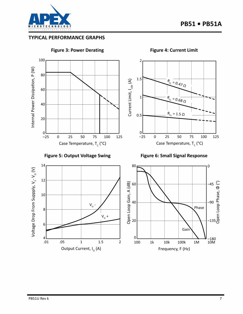
TYPICAL PERFORMANCE GRAPHS
Figure 3: Power Derating Figure 4: Current Limit
Figure 5: Output Voltage Swing Figure 6: Small Signal Response
Case Temperature, TC (°C)–25 0 25 50 75 1000
40
125
20
60
80
100
Case Temperature, TC (°C)
Curr
ent L
imit,
I LIM
(A)
–25 25 1250
1.5
2
1
0.5
0 50 75 100
RCL
RCL
RCL
Output Current, IO (A)
Volta
ge D
rop
From
Sup
pply
, VS- V
O (V
)
.01 .05 24
12
14
10
1 1.5
8
6
VO +
VO -
Frequency, F (Hz)
Ope
n Lo
op G
ain,
A (d
B)
100 10M0
60
20
40
80
1k 10k 100k 1M–180
–135
–90
–45
0
Phase
Gain
PB51U Rev k 7
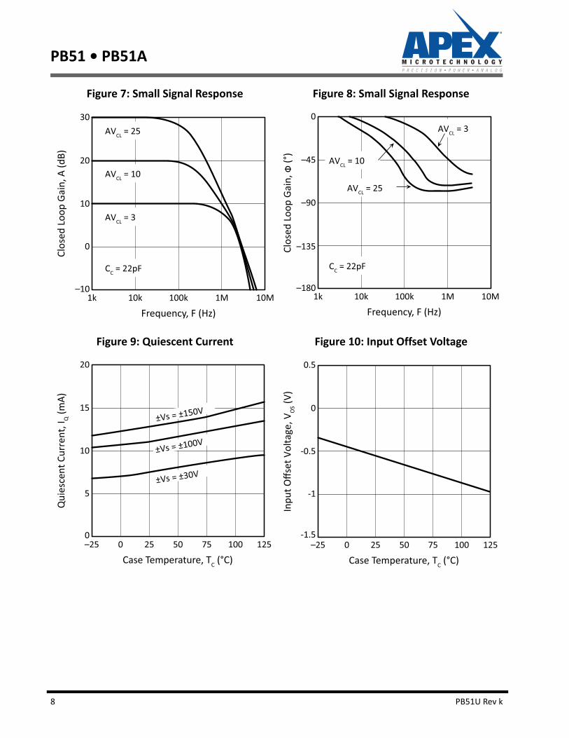
PB51 • PB51A
Figure 7: Small Signal Response Figure 8: Small Signal Response
Figure 9: Quiescent Current Figure 10: Input Offset Voltage
Frequency, F (Hz)
Clos
ed L
oop
Gain
, A (d
B)
1k 10k 10M–10
20
30
10
100k 1M
0
AVCL = 10
AVCL = 3
AVCL = 25
CC = 22pF
Frequency, F (Hz)
Clos
ed L
oop
Gain
, (°
)1k 10k 10M
–180100k 1M
–135
–90
–45
0
AVCL = 25
AVCL = 10
AVCL = 3
CC = 22pF
Case Temperature, TC (°C)
Qui
esce
nt C
urre
nt, I
Q (m
A)
–25 750
20
1000 25 50 125
5
10
15
±Vs = ±100V
±Vs = ±30V
±Vs = ±150V
Case Temperature, TC (°C)
OS
-1.5
-1
-0.5
0
0.5
–25 75 1000 25 50 125
8 PB51U Rev k

PB51 • PB51A
Figure 11: Slew Rate vs. Temperature Figure 12: Power Response
Figure 13: Pulse Response Figure 14: Harmonic Distortion
Case Temperature, TC (°C)
Slew
Rat
e, S
R (V
/μs)
0
300
400
100
200
–25 75 1000 25 50 125
-SLEW
+SLEW
Frequency, F (Hz)O
utpu
t Vol
tage
, VQ (V
P-P)
100k 1M 10M10
300
20
100
200
300k 3M
304050
Time, t (μs)
Out
put V
olta
ge, V
Q (V
)
1-80
2 3 4 5 6 7 8
-60
-40
-20
0
20
40
60
80
Frequency, F (Hz)
%)
300 3k 30k.001
0.1
.01
.03
1k
.003
10k
VS = 60VVO = 95VP-P
R
R
PB51U Rev k 9

PB51 • PB51A
SAFE OPERATING AREA (SOA)
Note: The output stage is protected against transient flyback. However, for protection against sustained,high energy flyback, external fast-recovery diodes should be used.
Figure 15: SOA
S O
SS
C = 25°CC = 85°C
C = 125°C
3
2
1
.2
.3
.4
.5
10 20 30 40 50 100 200 300.1
10 PB51U Rev k

PB51 • PB51A
GENERAL
Please read Application Note 1, “General Operating Considerations” which covers stability, supplies, heatsinking, mounting, current limit, SOA interpretation, and specification interpretation. Visit www.apexana-log.com for Apex Microtechnology’s complete Application Notes library, Technical Seminar Workbook, andEvaluation Kits.
TYPICAL APPLICATION
Figure 16: Typical Application
CURRENT LIMIT
For proper operation, the current limit resistor (RCL) must be connected as shown in the external connec-
tion diagram. The minimum value is 0.33 with a maximum practical value of 47. For optimum reliability theresistor value should be set as high as possible. The value is calculated as follows:
COMPOSITE AMPLIFIER CONSIDERATIONS
Cascading two amplifiers within a feedback loop has many advantages, but also requires careful consider-ation of several amplifier and system parameters. The most important of these are gain, stability, slew rate,and output swing of the driver. Operating the booster amplifier in higher gains results in a higher slew rateand lower output swing requirement for the driver, but makes stability more difficult to achieve.
ICL0.65VRCL-------------- 0.01A+= ICL
0.65VRCL--------------=–
PB51U Rev k 11

PB51 • PB51A
GAIN SET
The booster’s closed-loop gain is given by the equation below. The composite amplifier’s closed loop gainis determined by the feedback network, that is: –Rf/Ri (inverting) or 1+Rf/Ri (non-inverting). The driver ampli-fier’s “effective gain” (Av) is equal to the composite gain divided by the booster gain.
Example: Inverting configuration (figure 17) withRi = 2 k, Rf = 60 k, Rg = 0:Av (booster) = (6.2 k/3.1 k) + 1 = 3Av (composite) = 60 k/2 k = – 30Av (driver) = – 30/3 = –10
Figure 17: Composite Amplifier Example
RG Av 1– 3.1k 6.2k–=
AvRG 6.2k+3.1k
------------------------ 1+=
12 PB51U Rev k

PB51 • PB51A
STABILITY
Stability can be maximized by observing the following guidelines:1. Operate the booster in the lowest practical gain.2. Operate the driver amplifier in the highest practical effective gain.3. Keep gain-bandwidth product of the driver lower than the closed loop bandwidth of the booster.4. Minimize phase shift within the loop.
A good compromise for (1) and (2) is to set booster gain from 3 to 10 with total (composite) gain at leasta factor of 3 times booster gain. Guideline (3) implies compensating the driver as required in low compositegain configurations. Phase shift within the loop (4) is minimized through use of booster and loop compensa-tion capacitors Cc and Cf when required. Typical values are 5pF to 33pF.
Stability is the most difficult to achieve in a configuration where driver effective gain is unity (ie; total gain= booster gain). For this situation, Table 1 gives compensation values for optimum square wave responsewith the op amp drivers listed.
Table 1: Example Drivers
SLEW RATE
The slew rate of the composite amplifier is equal to the slew rate of the driver times the booster gain,with a maximum value equal to the booster slew rate.
OUTPUT SWING
The maximum output voltage swing required from the driver op amp is equal to the maximum outputswing from the booster divided by the booster gain. The Vos of the booster must also be supplied by thedriver, and should be subtracted from the available swing range of the driver. Note also that effects of Vosdrift and booster gain accuracy should be considered when calculating maximum available driver swing.
DRIVER CCH CF CC FPBW SROP07 - 22p 22p 4kHz 1.5741 - 18p 10p 20kHz 7LF155 - 4.7p 10p 60kHz >60LF156 - 4.7p 10p 80kHz >60TL070 22p 15p 10p 80kHz >60For: RF = 33K, RI = 3.3K, RG = 22K
TYPICAL VALUES FOR CASE WHERE OP AMP EFFECTIVE GAIN = 1.
PB51U Rev k 13

PB51 • PB51A
PACKAGE OPTIONS
PACKAGE STYLE DP
Part Number Apex Package Style Description
PB51 DP 12-pin SIP
PB51A DP 12-pin SIP
PB51EE EE 12-pin SIP w/ formed leads
14 PB51U Rev k

PB51 • PB51A
PACKAGE STYLE EE
PB51U Rev k 15

PB51 • PB51A
16 PB51U Rev k
NEED TECHNICAL HELP? CONTACT APEX SUPPORT! For all Apex Microtechnology product questions and inquiries, call toll free 800-546-2739 in North America. Forinquiries via email, please contact [email protected]. International customers can also requestsupport by contacting their local Apex Microtechnology Sales Representative. To find the one nearest to you,go to www.apexanalog.com
IMPORTANT NOTICE
Apex Microtechnology, Inc. has made every effort to insure the accuracy of the content contained in this document. However, the information is
subject to change without notice and is provided "AS IS" without warranty of any kind (expressed or implied). Apex Microtechnology reserves the right
to make changes without further notice to any specifications or products mentioned herein to improve reliability. This document is the property ofApex Microtechnology and by furnishing this information, Apex Microtechnology grants no license, expressed or implied under any patents, mask
work rights, copyrights, trademarks, trade secrets or other intellectual property rights. Apex Microtechnology owns the copyrights associated with the
information contained herein and gives consent for copies to be made of the information only for use within your organization with respect to ApexMicrotechnology integrated circuits or other products of Apex Microtechnology. This consent does not extend to other copying such as copying for
general distribution, advertising or promotional purposes, or for creating any work for resale.
APEX MICROTECHNOLOGY PRODUCTS ARE NOT DESIGNED, AUTHORIZED OR WARRANTED TO BE SUITABLE FOR USE IN PRODUCTS USED FOR LIFESUPPORT, AUTOMOTIVE SAFETY, SECURITY DEVICES, OR OTHER CRITICAL APPLICATIONS. PRODUCTS IN SUCH APPLICATIONS ARE UNDERSTOOD TO BE
FULLY AT THE CUSTOMER OR THE CUSTOMER’S RISK.
Apex Microtechnology, Apex and Apex Precision Power are trademarks of Apex Microtechnology, Inc. All other corporate names noted herein may betrademarks of their respective holders.