Embed Size (px)
Citation preview

PCB-Embedded Phase Current Sensor and Short-Circuit
Detector for High Power SiC-Based Converters
Slavko Mocevic
Thesis submitted to the faculty of the Virginia Polytechnic Institute and State University
in partial fulfillment of the requirements for the degree of
Master of Science
In
Electrical Engineering
Dushan Boroyevich
Rolando Burgos
Guo-Quan (G.Q.) Lu
May, 8h, 2018
Blacksburg, Virginia
Keywords: SiC MOSFET, Rogowski coil, switch current sensor, phase current sensor,
short-circuit protection, desaturation
© 2018, Slavko Mocevic

PCB-Embedded Phase Current Sensor and Short-Circuit
Detector for High Power SiC-Based Converters
Slavko Mocevic
ABSTRACT
Nowadays, major public concern is concentrated on reducing the usage of
fossil fuels and reducing emissions of CO2 by different energy advancement.
Electric vehicle technology presents extremely effective way of reducing carbon
emissions and paves the way of having sustainable and renewable energy future.
In order to wear the cost of electric vehicles down, batteries have to be improved
as well as higher power density and high reliability has to be achieved. This
research work mainly focuses on achieving higher power density and higher
reliability of the inverter stage by utilizing wide-bandgap SiC MOSFET
semiconductor devices in electric vehicle application.
In order to achieve higher reliability of the inverter stage, high bandwidth,
high performance Rogowski coil switch current sensors are employed. These
sensor were embedded on the PCB and integrated on the gate driver. High
bandwidth switch current sensor measurement is used for fast short-circuit
detection and protection of the SiC MOSFET semiconductor switches.
Furthermore, comparison with conventional detection and protection method

used in automotive IGBT applications is shown where novel protection showed
superior performance.
This thesis also shows principle of how to obtain phase currents of the system
using Rogowski coil switch current sensor measurements. Digital reconstruction
principle is employed to obtain the phase currents. Accurate and linear current
sensor is achieved. By successfully realizing this integrated phase current
measurement on the gate driver, elimination of the commercial current sensors
from the system is possible. By eliminating existing phase current sensors, higher
power density could be achieved. Sensor is evaluated in both continuous and
discontinuous PWM schemes.

PCB-Embedded Phase Current Sensor and Short-Circuit
Detector for High Power SiC-Based Converters
Slavko Mocevic
GENERAL AUDIENCE ABSTRACT
Together with renewable sources, electric vehicle will play an important role
as a part of sustainable and renewable energy future by significantly reducing
emissions of CO2 into the atmosphere. In order to make electric cars more
acceptable and accessible and make a significant impact on the environment, cost
must be lowered down. To wear the cost of the electric vehicles down, powertrain
of the car must be significantly improved and made smaller as well as lighter.
This thesis mainly focuses on improving the reliability of the motor driving stage
by implementing novel protection during fault periods such as short-circuit
event. Furthermore, this novel protection allows current sensing that is crucial
for motor control during normal operation periods. This will enable more
compact motor driving stage since existing current sensing elements can be
eliminated.

Slavko Mocevic
v
Acknowledgement
First, I would like to thank my advisor, Dr. Dushan Boroyevich, for his support, guidance and
advising. He led me and helped me to acquire the valuable knowledge in this field, which for I am
forever grateful. It was my great honor and privilege to have the opportunity to pursue my degree
with him as my advisor at the Center for Power Electronics Systems (CPES).
I would also like to express my sincere gratitude to my co-advisor, Dr. Rolando Burgos for his
guidance in research and continuous support. His advices and suggestions during our weekly
meetings were of most importance to overcome research difficulties.
Many thanks to my committee member Dr. G.Q. Lu who provided useful feedback that has
helped me and my research.
I would also like to thank to the CPES staff Ms. Marianne Hawthorne, Ms. Teresa Shaw, Ms.
Trish Rose, Ms. Linda Long, Ms. Lauren Shutt and lab manager Mr. David Gilham for their help
and assistance.
It is my great honor to have worked with a group of brilliant people in CPES. I really enjoyed
the time of working with them and appreciate our friendship. These people are Dr. Jun Wang, Mr.
Joseph Kozak, Mr. Victor Turriate, Ms. Amy Romero, Mr. Mudit Khana, Mr. Alex Chu, Mr. Paul
Rankin, Mr. Sungjae Ohn, Ms. Christina DiMarino, Dr. Niloofar Rashidi Mehrabadi, Dr. Alinaghi
Marzoughi, Mr. Qiong Wang, Mr. Chi Li, Dr. Chao Fei, Ms. Bingyao Sun, Dr. Syed Bari, Mr.
Keyao Sun, Ms. Ying Ying Gui Ms. Nidhi Haryani, Mr. Jianghui Yu, Mr. Yue Xu, Mr. Junjie
Feng, Mr. Ting Ge, Mr. Zichen Miao, Mr. Bin Li, Ms. Jiewen Hu, Ms. Ye Tang, Ms. Grace Watt,
Ms. Emma Raszmann, and Ms. Rebecca Rye. There are many other people who helped me but are
not listed here. I want to thank them also.

Slavko Mocevic
vi
My research work is supported by the General Motors (GM) and Department of Energy (DoE).
I would thank their sponsorship. I appreciate all of the guidance and insight you have provided.
Thank you Marsko Jaksic, Constantin Stancu, Brian Peaslee, Mehrdad Teimor, John Czubay, Sung
K Chung, He Niu, William Ivan, and many others.
To my friends, thank you for listening, offering me advice, and supporting me through this
entire process. Special thanks to Mladen Stanisic, Bogdan Dzonlaga, Goran Milic, Djordjo
Cosovic, Nikola Stanisic, Milan Sobot, Aleksandar Tica, Aleksandra Maksimovic, Ivana Jokic,
Andjela Bulajic, Ivana Radisic, Stefan Predojevic, Veljko Boljanovic, Aleksandar Kerekes, Iso
Maric, Mladen Babic, Akhil Infant, Jamal Ahmad Khan, Awad Abdelhalim, Athulya Simon,
Niloofar Heydarian and many others.
Finally, I must express my very profound gratitude to my parents Momcilo and Branka
Mocevic, to my sister Ksenija Zecar and her husband Goran Zecar for providing me with unfailing
support and continuous encouragement throughout my years of study and through the process of
researching and writing this thesis. Also, special thanks to Slobodan Gataric and Milan Mocevic,
and rest of my family. This accomplishment would not have been possible without them. Thank
you.

Slavko Mocevic
vii
Table of Contents
Chapter 1 Introduction..................................................................................................... 1
1.1 Background ............................................................................................................. 1
1.2 Review of the Current Sensing Technologies ......................................................... 3
1.2.1 Motivation ............................................................................................................... 3
1.2.2 Current Sensors Review .......................................................................................... 4
1.3 Review of the Switch Short-Circuit Protections ..................................................... 9
1.3.1 Motivation ............................................................................................................... 9
1.3.2 State-of-the-art Short-Circuit protection for SiC MOSFETs ................................ 13
1.4 Thesis Outline ....................................................................................................... 19
Chapter 2 Gate Driver Architecture and Functional Circuit Design ........................ 21
2.1 Introduction ........................................................................................................... 21
2.2 Phase Current Reconstruction Principle ............................................................... 22
2.3 Gate Driver Architecture ...................................................................................... 25
2.4 Functional Circuit and Rogowski Switch Current Sensor Design ........................ 30
2.4.1 Functional Circuit Design ..................................................................................... 30
2.4.2 Rogowski Switch Current Sensor Design ............................................................. 33
2.4.3 Prototype ............................................................................................................... 36
Chapter 3 Phase Current Reconstruction and Sensor Performance ......................... 38
3.1 Introduction ........................................................................................................... 38
3.2 Detailed Block Diagram of Digital Phase Current Reconstruction ...................... 38
3.3 Phase Current Sensor Performance ....................................................................... 41
3.3.1 Concept Verification in Double Pulse Test (DPT) ................................................ 41
3.3.2 RSCS and Phase Current Sensor Error Diagrams ................................................. 44

Slavko Mocevic
viii
3.4 Phase Current Sensor Performance in Inverter Applications ............................... 46
3.4.1 Phase Current Sensor Performance in Continuous PWM Inverter ....................... 46
3.4.2 Phase Current Sensor Performance in Discontinuous PWM Inverter ................... 52
3.5 Influence of Adjacent Phases on Rogowski Coils ................................................ 59
3.5.1 Electrical Influence ................................................................................................ 59
3.5.2 Magnetic Influence ................................................................................................ 62
Chapter 4 Short-Circuit protection performance ........................................................ 66
4.1 Introduction ........................................................................................................... 66
4.2 Types and Behavior of Short-Circuit in the Half-Bridge Configuration .............. 67
4.2.1 Shoot-through Type of Short-Circuit .................................................................... 67
4.2.2 Load Fault Type of Short-Circuit .......................................................................... 68
4.2.3 Behavior during Short-Circuit Event..................................................................... 68
4.3 Detection and Protection Mechanism ................................................................... 71
4.4 Two-level Turn-off (2LTO) Design ..................................................................... 73
4.4.1 Background ........................................................................................................... 73
4.4.2 Design Goals and Terminology ............................................................................. 74
4.4.3 Experimental Results and Conclusion ................................................................... 76
4.5 Experimental Results ............................................................................................ 80
4.5.1 Experimental Setup ............................................................................................... 80
4.5.2 FUL ....................................................................................................................... 81
4.5.3 HSF ........................................................................................................................ 83
4.5.4 Load Fault .............................................................................................................. 85
4.6 Comparison with Desaturation Protection ............................................................ 86
4.6.1 Desaturation (DeSat) Protection Mechanism Principles ....................................... 86
4.6.2 Desaturation (DeSat) Protection Behavior during SC ........................................... 88
4.6.3 Comparison between RSCS and DeSat Protection Methods ................................ 91
Chapter 5 Conclusion ..................................................................................................... 95

Slavko Mocevic
ix
5.1 Summary and Conclusions ................................................................................... 95
5.2 Future Work .......................................................................................................... 97
References ........................................................................................................................ 98
Publications ................................................................................................................... 103
Appendix A – Short-circuit Performance during Clamped Period of DPWM ....... 104

Slavko Mocevic
x
List of Figures Figure 1 – Commercial Hall-effect sensor.................................................................................... 3
Figure 2 - Overview of different current sensing techniques....................................................... 4
Figure 3 - Withstand times of SiC MOSFET and Si IGBT ......................................................... 9
Figure 4 - Output characteristics comparison: Si IGBT vs. SiC MOSFET .............................. 11
Figure 5 - SSCB overcurrent protection circuit ......................................................................... 13
Figure 6 - SiC MOSFET chip with current sense terminal ....................................................... 14
Figure 7 – Circuit configuration of the proposed detection method.......................................... 15
Figure 8 – GD with implemented parasitic inductance SC protection and circuit schematic .. 16
Figure 9 - Rogowski coil PCB embedded implementation and principle of work schematic ... 17
Figure 10 – Phase current reconstruction principle .................................................................. 23
Figure 11 – Obtaining the phase current: a) analog reconstruction, b) digital reconstruction 24
Figure 12 - Architecture with analog reconstruction, RSCS-s on controller ground ............... 26
Figure 13 - Architecure with digital reconstruction, RSCS-s on controller ground ................. 26
Figure 14 - Architecture with digital reconstruction, RSCS-s on isolated ground ................... 27
Figure 15 - Architecture with analog reconstruction, RSCS-s on isolated ground .................. 27
Figure 16 - Schematics of the paralleled current boosters......................................................... 31
Figure 17 - Active Miller clamp design ....................................................................................... 32
Figure 18 - Conceptual structure of Rogowski coils .................................................................. 34
Figure 19 - Rogowski coil layer design on a 6-layer PCB ......................................................... 34
Figure 20 - Rogowski coil layout ................................................................................................. 35
Figure 21 - Signal processing circuit of RSCS ........................................................................... 36
Figure 22 - Top view of GD prototype ......................................................................................... 37
Figure 23 - Bottom view of GD prototype ................................................................................... 37
Figure 24 - Detailed block diagram of digital phase current reconstruction ............................ 39
Figure 25 - Simplified schematic of a DPT ................................................................................ 41
Figure 26 - Double pulse test waveforms .................................................................................... 42

Slavko Mocevic
xi
Figure 27 - Double pulse test results and phase (inductor) current delay ................................ 43
Figure 28 - Comparison with the commercial Rogowski current probe.................................... 44
Figure 29 - Resulting error diagram ........................................................................................... 45
Figure 30 - Experimental inverter test setup .............................................................................. 47
Figure 31 - Reconstructed phase current of the inverter phase ................................................. 48
Figure 32 - Comparison with the commercial phase current measurement ............................. 49
Figure 33 - Frequency spectra of the 3 different phase current measurement techniques ...... 50
Figure 34 - Linearity error of the phase current sensor ............................................................ 52
Figure 35 - Behavior of sensors during DPWM ......................................................................... 53
Figure 36 - Conventional 60 degrees DPWM ............................................................................. 54
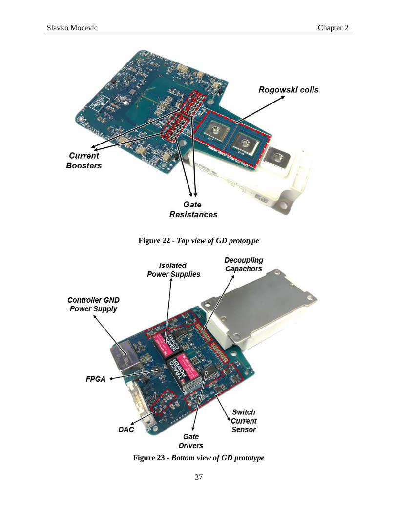
Figure 37 - DPWM scheme phase current waveforms ............................................................... 55
Figure 38 - Sensor during DPWM reconstruction principle ..................................................... 56
Figure 39 – Analog DPWM current reconstruction verification ............................................... 57
Figure 40 - Current reconstruction algorithm for phase C ....................................................... 58
Figure 41 - Values of reconstructed currents stored in controller registers ............................. 59
Figure 42 – Schematic and hardware for influence investigation ............................................ 60
Figure 43 - Experimental results from electric influence of adjacent phases........................... 61
Figure 44 - Spectrum of bottom Rogowski coil output in phase B ............................................ 61
Figure 45 - Experimental results from magnetic influence of adjacent phases ....................... 63
Figure 46 – Spectral analysis results for magnetic influence .................................................... 64
Figure 47 - Spectral analysis results for magnetic influence with environmental noise results
....................................................................................................................................................... 65
Figure 48 - Types of SC in the half-bridge configuration.......................................................... 67
Figure 49 - Experimental waveforms in short-circuit without protection ................................. 69
Figure 50 - Rogowski switch current sensor protection mechanism ......................................... 71
Figure 51 – 2LTO test waveform to introduce terminology ....................................................... 75
Figure 52 - Behavior of 1st and 2nd voltage overshoot with varied 2LTO voltage and time ... 77

Slavko Mocevic
xii
Figure 53 - Dissipated energy contributed by 2LTO with varied 2LTO voltage and time ........ 78
Figure 54 - Comparison between maximum voltage peaks and dissipated energy ................... 79
Figure 55 - Experimental SC setup ............................................................................................. 81
Figure 56 - 600 V FUL experimental waveforms of RSCS protection ...................................... 82
Figure 57 - 600 V HSF experimental waveforms of RSCS protection ...................................... 84
Figure 58 - 600 V Load fault experimental waveforms of RSCS protection ............................. 85
Figure 59 - Desaturation protection circuit ................................................................................ 87
Figure 60 - 600 V FUL experimental waveforms of DeSat protection ...................................... 88
Figure 61 - 600 V HSF experimental waveforms of DeSat protection ...................................... 90
Figure 62 - 600 V load fault experimental waveforms of DeSat protection .............................. 90
Figure 63 - FUL comparison between protections ..................................................................... 92
Figure 64 - HSF comparison between protections ..................................................................... 93
Figure 65 - Load fault comparison between protections ............................................................ 94
Figure 66 - Integrator OpAmp without input offset compensation circuit.............................. 105
Figure 67 - Integrator OpAmp with input offset compensation circuit ................................... 105
Figure 68 - Two possible cases of SC during clamped period of DPWM ................................ 106
Figure 69 – Gate Signals for DPWM SC case .......................................................................... 107
Figure 70 - SC event during clamped period of DPWM .......................................................... 108

Slavko Mocevic Chapter 1
1
Chapter 1 Introduction
1.1 Background
Major public concern is the need of advancing energy technology in order to conserve
natural resources and use clean energy as much as possible. This will reduce usage of fossil fuels
and thus reduce emissions of CO2. Furthermore, energy efficiency raise is also crucial since
worldwide demand for electrical energy is inevitably increasing. One of the major parts in
achieving this sustainable and renewable energy future is electric vehicle (EV). Besides the fact
that EV presents extremely effective way of reducing carbon emissions, advantages also include
higher efficiency of drivetrain, reduced fuel cost, low noise level, reliability and less maintenance.
According to the Global EV Outlook report from 2017 [1], EV stock surpassed 2 million vehicles
and will reach roughly 20 million by 2020 and between 40 and 70 million by 2025. Besides
infrastructure, high battery cost, in order to bring the cost down, increase of efficiency and
reliability as well as additional improvement in EV motor drive have to be achieved.
The general market and technology trends in electric vehicles and hybrid electric vehicles
(HEV), are striving to achieve high density and high efficiency conversion [1], [2]. For motor-
drive applications, integrating silicon carbide (SiC) power MOSFETs has become an attractive
solution due to their high breakdown electric field, high working temperature, fast switching speed
and low on-state resistance [3], [4], [5]. Fast switching speed and low switching losses enables
high switching frequency operation, which improves the power density of high power converters.
Moreover, since switching frequency could be increased, bulky passive components size reduction

Slavko Mocevic Chapter 1
2
is possible. In the past few years, cost of SiC MOSFET is decreasing due to the increased usage in
industry applications and due to their growing mass production. Considering these facts, overall
system cost will become comparable or even lower than conventional Si-based designs due to the
reduced material cost [6]. Therefore, SiC MOSFET presents great potential in medium-voltage
(MV) high power applications, and can potentially substitute MV IGBT devices [7]. However,
simple change from IGBT to SiC technology is not simple and fast as it sounds. Amongst other
things that still raise concern about SiC, its driving technology must satisfy following
requirements: isolation, fast switching of the device by supplying sufficient gate current, high noise
immunity, low propagation delay, and fast low-level protection. Major challenges for these gate
drivers (GD) are making it robust and providing reliable operation of the SiC MOSFET device.
To further push power density and to reduce overall system cost and weight, other aspects of
inverter besides just simple change of IGBT devices could be investigated. Sensors, as a crucial
part of control loops of inverter, could be possibly appropriated for SiC inverter applications.
Reducing number of sensors, as well as increasing power density and reliability should be pursued
to wear the price down.
Aim of this thesis is to design a GD with fast short-circuit protection based on switch current
measurement, as well as the integrated phase current measurement. Therefore, this chapter would
like to discover what current sensing technologies in high current inverter applications are being
used. Literature review of state-of-the-art current sensor is presented in order to find out which
method will be able to increase power density and reliability as well as to reduce cost and weight.
Furthermore, state-of-the-art short-circuit protection literature survey is done in order to obtain
knowledge about SiC MOSFET protection methods that are currently being used by either industry
or researchers. Also, motivations for this research work and the thesis outline are presented.

Slavko Mocevic Chapter 1
3
1.2 Review of the Current Sensing Technologies
1.2.1 Motivation
In automotive motor-drive inverter applications the Hall-effect sensor (Figure 1) is standard
for control purposes current measurement due to high linearity (< 1%), high sensor accuracy (<1
%), simplicity and isolation capabilities (non-intrusive current measurement method). In these
applications three phase currents are measured for control. In order to increase power density of
the system, increase reliability (reducing component size, wiring etc.), decrease cost of the system
(Hall-effect sensors are very expensive), elimination of Hall sensor in future high power density
power electronics applications in inevitable. Moreover, Hall-effect sensor are susceptible to
external magnetic fields. Knowing the phase current is essential in inverter applications. Thus
phase current measurement or at least bottom switch current measurement with reconstruction
algorithm on controller to obtain phase current measurement must be preserved. Therefore, current
sensing technologies were reviewed in the next subchapter to find most suitable phase current
measurement that would result in higher power density by integrating it on GD.
Figure 1 – Commercial Hall-effect sensor
Slavko Mocevic Chapter 1
4
1.2.2 Current Sensors Review
To enable enhanced performance of power electronics applications through the current
feedback loop, current measurement transducers have always been designed to be state-of-the-art.
Nowadays, requirements for the current sensing devices in inverters are high rated current, high
density, high isolation capabilities, accuracy under 1% for a wide range of operating temperatures,
and CM noise immunity in response to the emerging faster-switching power devices [8],[9]. There
are many ways to monitor current including intrusive (non-isolated) and non-intrusive
(isolated/differential) methods, as shown in Figure 2.
Figure 2 - Overview of different current sensing techniques
In inverter applications, widely used phase current measurements are Hall-effect sensors,
current shunts, current transformers and Rogowski coils due to benefits that they exhibit.
In industrial motor drives, the Hall-effect sensor (suitable for both DC and AC measurements)
is the standard for phase current measurement due to its simplicity, accuracy, reliability, hassle-

Slavko Mocevic Chapter 1
5
free maintenance and fully isolated structure. Widely used simple, inexpensive and compact open-
loop Hall-effect sensor are nowadays being replaced with closed loop technology due to their
problems with proportionality, susceptibility to external magnetic field, bandwidth, losses etc. In
a closed-loop configuration the output voltage of the magnetic field sensor is used as an error
signal to compensate the magnetization inside the magnetic core by forcing a current through a
secondary transformer winding. This technique greatly reduces the influence of the thermal drift
of the magnetic field sensing device. The linearity also becomes independent of the magnetic field
sensor. Another benefit of the closed loop sensor is that because the core magnetization is
theoretically zero there are no eddy current or hysteresis losses. However, due to higher density
trends in power electronics, these transducers are considered bulky, expensive, have more
complicated construction and are susceptible to stray external magnetic fields up to some extent
[10], [11], [12], [13].
In order to reduce the number of sensors and overall cost, the simplest and most cost-effective
alternative is the use of current shunts, which are suitable for both DC and AC measurements. In
inverter applications for motor-phase current sensing, commonly used methods are: inline phase
current sensing, inverter leg current sensing, and DC bus current sensing using single shunt. Very
rarely current shunts are inserted in the actual phases (inline phase current sensing) to measure
currents due to problems that will arise with the isolation of the measurement and other possible
difficulties. Most common method considering shunt measurements is when they are configured
in series with bottom power devices in the module located on the source. Three or two shunt
techniques are possible, but regardless of the shunt configuration used, current can only be
measured when a bottom switch is ON. Most cost-efficient solution is to implement a single shunt
resistor inserted in the negative DC bus. However, this requires specifically PWM pattern in order

Slavko Mocevic Chapter 1
6
to extract the current information, which may be intolerable for some of the applications. The
biggest drawbacks of using shunts are that they are intrusive to the circuit and they introduce
additional losses to the system. Therefore, due to recent high efficiency trend, using current shunts,
which are intrusive to circuit, cannot be usually justified since they introduce additional loss and
can severely reduce inverter efficiency especially in high power applications [11], [14], [15].
Furthermore, for realizing next generation circuit using SiC and GaN, use of such current methods
is unacceptable since it will insert additional parasitic inductance in the system, which may degrade
switching performance.
Current transformers (CT) have been widely used for AC current sensing with its bandwidth
up to tens of MHz. This sensing technique provides galvanic isolation, consumes little power, low
losses, and simple working principle. CTs are very popular in some of the low power conversion
applications (even with the demagnetizing circuit employed) because of their low cost, and ability
to provide an output signal that is directly compatible with an analog-to-digital converter. Even
though the current transformer does not insert any loss in the power stage, due to its bulkiness,
lower accuracy, and inability to measure DC currents, this type of measurement is not popular in
inverter applications [10], [11], but is sometimes used. They are also intensively employed in
power distribution networks at 50/60 Hz line frequency.
The Rogowski coil is a non-intrusive method of measuring AC currents, but is usually unable
to measure low frequency (<20Hz) or DC currents, because basic principle of operation is based
on detection of flux change, utilizing Faraday’s law of induction. On the other hand, it is able to
measure very high frequency, very high currents with the same coil size without saturation (due to
its air core), and has good linearity due to absence of magnetic material. Also, it is compact and
light weight. It is especially useful in situations where the amplitude of the current pulse is

Slavko Mocevic Chapter 1
7
unknown. Rogowski coils can be applied to measure currents in power distribution systems, short-
circuit testing systems, electromagnetic launchers, slip-ring induction motors, and lightning test
facilities. However, due to its poor performance at low frequencies, drooping effect and thermal
drift of the integrator, it is not extensively used in inverter applications [10], [11], [12].
Current sensing techniques such as inductor internal resistance, filter based inductor DCR,
senseFET as well as magneto-resistor method are not used in the inverter applications almost at
all.
Magneto-resistive structures such as Anisotropic Magneto-resistive (AMR) and Giant
Magneto-resistive (GMR) are structures in which the electrical resistance varies as a function of
applied magnetic field. Therefore, these structures can be used as magnetic field sensors. Due to
their high sensitivity to the magnetic field, the AMR and GMR sensors can be effectively used to
sense the current by measuring the magnetic field generated by the current. Magneto-resistors were
previously used extensively in magnetometry, as the read head in magnetic recording etc. Due to
their inherent capability of being able to respond to very high frequency magnetic excitations,
recently they are gaining rapid popularity as current sensors in high frequency applications [16]-
[19]. Characteristics preventing them for wide utilization in inverter applications are: high thermal
drift, high non-linearity, extreme susceptibility to external magnetic fields and still high cost.
To employ current mirror techniques, particular devices in inverter have to be used.
Semiconductor switches beside normal current carrying dies, would have to have an additional die
embedded just for current mirroring. Current going through that current sensing output is directly
proportional to the current through the switch. Even though this method presents high accuracy
and high bandwidth current measurement technique, due to a possible high thermal drift as well

Slavko Mocevic Chapter 1
8
as high initial cost of using this particular type of semiconductor switch, this method is not that
much utilized in the inverter application [20], [21], [22].
Often used in low voltage, high current applications (especially in VRM applications) is filter
based inductor DCR current sense technique since current shunt cannot be used in high-current
VRMs due to the significant losses caused by the power dissipation. Figure 1 in [23] shows the
sense circuit where the inductor DCR is utilized to measure the current circulating through it. Thus,
voltage on the capacitor is proportional to inductor current [23], [24], [25]. However, since this
method is inapplicable in inverter application as well as the inductor resistance method, it will not
be further discussed.
Recently, there were many hybrid methods emerging. Hybrid methods are usually combination
of the mentioned current sensing techniques in order to overcome some of the flaws that they have
looking at them individually. Usually, bandwidth, DC component as well as thermal drift and
linearity are areas that these hybrid sensor aim to improve. Many of them can be found in literature
[26], [27], [28], [29] etc.
As mentioned before, in industrial high power inverter applications Hall-effect sensors, current
shunts, current transformers and Rogowski coils are widely employed. In order to improve power
density of inverter stage in EV applications, as well as reliability and reduce cost, integration of
phase current sensor on the GD would definitely be one of the best choices. In that case, best
candidates to PCB-embed and integrate on GD would be either Hall-effect sensor, Rogowski coil,
or CT. In the next subchapter, literature review of the short-circuit protection will be conducted
and best method of current sensing will be chosen to both protect devices and provide phase current
feedback.

Slavko Mocevic Chapter 1
9
1.3 Review of the Switch Short-Circuit Protections
1.3.1 Motivation
Failure modes such as short-circuit (SC) can potentially cause excessive currents and excessive
power dissipation which very quickly overheats the power module and destroys it. In order to
prevent catastrophic damage, detection and protection must be implemented to reduce or turn-off
the overcurrent (OS) during the fault condition [30]. It is even more critical in medium voltage
high power application as the components are expensive and high-energy explosion is catastrophic
[6]. In the event of SC, the GD circuit must be able to detect the fault condition and safely shut the
device off before a failure of the device occurs [31].
Figure 3 shows that when SC occurs, SiC MOSFETs can only withstand several μs,
evidencing for most of the cases lower robustness than the Si IGBT counterpart, where the typical
SC withstanding time is 10 μs at the highest operating temperature [32], [33]. This comparison is
done for comparable devices of 1.2 kV, 300A. From thermal point of view, this lower short-circuit
withstand capability for SiC MOSFET device is completely expected due to a smaller chip area
and higher current density than Si IGBT device, as well as higher currents during short-circuit (10-
15 times rated current).
Figure 3 - Withstand times of SiC MOSFET and Si IGBT

Slavko Mocevic Chapter 1
10
Based on observation from previous figure, and literature [34] and [35] whichever detection
method and protection mechanism is used, its implementation needs to have following targets:
• Fast detection and reaction time which will impact the current peak level, limiting the
overheating and current stresses
• Responsive for all SC types and not degrade conduction or switching characteristics
• Turn-off in a safe manner
• Inexpensive and easy implementation\integration in any GDdesign
• Robust and high noise immunity
Several conventional methods of realizing SC protection for the MV high power IGBT
applications exists. Collector-emitter voltage measurement over the IGBT, called desaturation
method (DeSat) is one of them. It is also possible to use current sense IGBTs in which a fraction
of IGBT cells in the chip are used for observing current going through device. Intelligent power
modules often utilize such a solution. Another possibility is to analyze the gate voltage of the IGBT
or the behavior of the gate charge at turn-on. The SC affects the gate voltage and this property can
be used in fast fault monitoring. The fourth way for protecting IGBT is based on the measurement
of the collector current. Current measurement can be done e.g. by a shunt resistor, a current
transformer, a Rogowski coil or by voltage measurement over the power module parasitic
inductance [36]. The most used type of short-circuit protection for IGBT applications was DeSat
protection due to low implementation cost, simplicity and effectiveness. Naturally, people would
like to use it for SiC MOSFET applications also. However, this type of protection may not be
suitable for these devices due to several reasons.
First, DeSat protection method is taking advantage of IGBT’s output characteristics. Figure 4
shows output characteristics of Si IGBT and SiC MOSFET rated for same voltage and current.

Slavko Mocevic Chapter 1
11
Figure 4 - Output characteristics comparison: Si IGBT vs. SiC MOSFET
When a short-circuit happens, IGBTs show a sharp (“hard”) turning point from the saturated to the
desaturated (linear) region in the output characteristic. In the desaturated state, failure current is
limited to up to 3-5 times the rated current making 𝑉𝑐𝑒 sense simple, easy-to-implement, robust,
and reliable since device can withstand these severe conditions up to 10 μs. However, the output
characteristics of the SiC MOSFET are “softer” in transition region. Figure 3 and Figure 4 show
that the fault current 𝐼𝐷 can quickly rise up to values above 10𝑥𝐼𝑑𝑟𝑎𝑡𝑒𝑑 even when the drain-source
voltage 𝑉𝐷𝑆 is at high values. Accumulated short-circuit energy on the SiC MOSFET is extensively
higher the Si IGBTs, and can withstand these severe conditions several μs, evidencing lower
robustness than their Si IGBT counterpart. Consequently, DeSat would have to be tuned to react
very fast and precise, which is in some cases very difficult for SiC applications due to a blanking
time.
Second, DeSat protection method requires necessary blanking time. This is mainly because
DeSat circuitry has to start functioning after 𝑉𝐶𝐸 drops to zero and all turn-on oscillations pass.

Slavko Mocevic Chapter 1
12
The time span between the gate signal turning on and until DeSat pin on the GD starts sensing is
called “blanking time”. If this is not implemented, nuisance tripping of the protection would
probably be observed. For IGBT even if the SC event happens during this blanking time, due to
longer withstand time, it would not be a problem, and the device would have safely shut down.
For SiC MOSFET, due to fast switching nature and high slew rates of current and voltages, having
long blanking time is unacceptable. However, engineers often have to extend this blanking time to
dump noises coming from the system at the switching instances. The noise immunity and fault
response time then become sharp contradictions. This makes DeSat protection for SiC MOSFETS
hard to tune, making it less reliable protection method.
Third, DeSat protection also works well with varying junction temperature as the SiC IGBT
output characteristics are not highly dependent on the temperature, as shown in the comparison
between the 25𝑜𝐶 and 150𝑜𝐶 characteristics in the Figure 4. On the other hand, output
characteristics of SiC MOSFETs has almost 50% difference between 25°C and 150°C. This
behavior indicates that short-circuit current threshold varies distinctively if using 𝑉𝐷𝑆 -based
current sensing method. This fact presents possible problem for using DeSat protection in SiC
applications, since this protection is tuned for high temperature in order to avoid false tripping if
tuned for low temperature characteristics.
Forth, trend in new SiC MOSFET packages [37] is to have low internal inductances and low
on-state resistances such that switching as well as conduction losses could be minimized. However,
this reduction of inductance means that during an SC event less impedance be will opposing the
current. This will result in fast SC 𝑑𝑖/𝑑𝑡 which will cause the current to rise even more quickly
causing possible destruction of the module due to excessive dissipated energy or high overshoot

Slavko Mocevic Chapter 1
13
during the turn-off. Question is now weather DeSat will be able to turn the device safely in time
due to abnormal energy dissipation in a very short time.
Taking into account all of the previously discussed, researches are coming with alternatives to
DeSat protection to achieve fast and reliable SC performance of SiC devices.
1.3.2 State-of-the-art Short-Circuit protection for SiC MOSFETs
1.3.2.1 Improved DeSat protection
More and more researches are improving DeSat protection and modifying it in order to reduce
blanking time as much as possible and implementing other false triggering suppression methods
[34], [38], [39] etc. However, only effective SC protection with this method will be if blanking
time is set to be less than 300ns, which is sometimes very hard to achieve in the SiC applications,
due to high noises coming from the power stage.
1.3.2.2 Solid State Circuit Breaker
Figure 5 shows experimental setup as well as circuit schematic of the solid state circuit breaker
(SSCB) [38].
Figure 5 - SSCB overcurrent protection circuit

Slavko Mocevic Chapter 1
14
Normally-on SSCB is taking advantage of the well-known DeSat protection scheme of the IGBTs.
Regardles of its drawbacks, which are high cost, auxiliary power supply, incompatibility with the
laminated busbar dc link, and high power dissipation, the SSCB is used as a universal protection
method, even without knowing the specific characteristics of power device in the converters. The
SSCB could be inserted either in series with the energy storage capacitors (position A), or in series
with the main power loop (position B). Inserting it into the main power loop can reliably detect
and clear overcurrent faults, while considerable power dissipation is a concern. At position A, the
loss associated with the SSCB is small since only ripple current goes through the SSCB in series
with the dc link energy storage capacitors. This method can reliably detect short-circuit in 0.5 μs
and effectively turn it off in less than 1.32 μs.
1.3.2.3 Current Mirror
Figure 6 shows SiC MOSFET chip with the current sense terminal [21].
Figure 6 - SiC MOSFET chip with current sense terminal

Slavko Mocevic Chapter 1
15
The 100A 1200V SiC MOSFET chips used in the FMF800DX-24A have an isolated source area
on top of the source metallization. This small source area is connected to the sense terminal. Thus
an earmarked portion of the total source is provided at the sense terminal. The monitored source
sense voltage across the sense and source terminals can be used for detecting overcurrents. The
current through the sense resistance is proportional to the main source current. The ratio between
the sense current and main source current is in the range of 1:61500. By considering this current
dependency and junction temperature dependency, an appropriate shunt resistor (RS) can be
selected setting the needed overcurrent trip level. Short-circuit was turned off in less than 1 μs.
1.3.2.4 Short-Circuit Protection Method using Gate Charge Characteristics
Figure 7 shows an outline of the protection circuit against SC conditions [40].
Figure 7 – Circuit configuration of the proposed detection method
As described in [40], there is noticeable difference in gate–source voltage waveforms between
normal conditions and under SC conditions. As a consequence, a gate charge characteristic under

Slavko Mocevic Chapter 1
16
SC conditions differs from that under normal operating conditions. Figure 7 shows that detection
monitors gate–source voltage 𝑉𝑔𝑠 and the voltage across gate resistor 𝑅𝑔. The detected voltage
across 𝑅𝑔 is transferred to a differential amplifier, and gate charge 𝑄𝑔 is calculated with an
integrator. Detected gate–source voltage 𝑣𝑑𝑒𝑡 and 𝑄𝑔 are compared with reference voltage 𝑉𝑟𝑒𝑓
and 𝑄𝑟𝑒𝑓 , respectively. The detection signal is a logical product of the output signals from
Comparator1 and Comparator2. The detection signal should be held by using a latch-circuit such
as a set-reset flip-flop (SRFF) because 𝑉𝑔𝑠 decreases after detecting the SC to protect the SiC
MOSFET from destruction. The inverting original gate control signal is transfered to the reset
terminal in an SRFF. The final gate signal “Y” is the logical product of the original gate control
signal “X1” and the inverting protection signal “X2”. Total time turn off time of implemented
detection and protection is around 1.5 μs.
1.3.2.5 Parasitic Inductance Method
Figure 8 GD with implemented parasitic inductance SC and OC detection method and circuit
schematic [36], [41].
Figure 8 – GD with implemented parasitic inductance SC protection and circuit schematic

Slavko Mocevic Chapter 1
17
This protection method requires modules and devices which have a four-terminal structure
where the Kelvin source is connected to the gate control signal and power source connected to the
power loop are separated. Utilizing parasitic inductance 𝐿𝑝 between Kelvin source and power
source for short-circuit protection in SiC MOSFET has been studied, and is able to detect the short-
circuit current at around 100 ns with proper design. As shown in the blue region of Figure 8 (SC
Detection Branch), a capacitor 𝐶𝑠 and a resistor 𝑅𝑠 is connected across the parasitic inductor 𝐿𝑝.
Therefore, the transfer function from the switching current 𝑖𝑑 to the voltage across 𝐶𝑠 can be
calculated as
𝐺𝑣𝑜𝑖𝑑(𝑠) ≈
𝐿𝑝
𝑅𝑠𝐶𝑠
Where 𝑣𝑜 will be proportional to 𝑖𝑑 if the high frequency components dominate the switching
current 𝑖𝑑. Therefore, the current through the SiC MOSFET module is transduced to a voltage
signal across the 𝐶𝑠 proportionally. Detection time reported was 80 ns, while total time spent in
SC including soft-turn off is 1.1 μs.
1.3.2.6 Rogowski Coil Detection Method
Figure 9 shows PCB embedded Rogowski coils and principle of work schematic [42].
Figure 9 - Rogowski coil PCB embedded implementation and principle of work schematic

Slavko Mocevic Chapter 1
18
The Rogowski coil serves as a differentiator that generates 𝑑𝑖/𝑑𝑡 value of the sensed current,
scaled by a factor of the mutual inductance between the sensed busbar and the coil. The integrator
works together with the coil to convert the 𝑑𝑖/𝑑𝑡 information back to the current information.
Active integrator is selected to obtain wider and higher BW even though it requires more complex
circuitry. Reset switch is also added in order to reset output to zero when SiC MOSFET is turned
off. Therefore, the transfer function from the switching current 𝑖𝑑 to the voltage 𝑣𝑜 is:
𝐺𝑣𝑜𝑖𝑑(𝑠) =
𝑀
𝑅𝐶
Where 𝑣𝑜 will be proportional to 𝑖𝑑. Detection time reported was 100 ns, while total time spent in
SC including soft-turn off is around 1.1 μs.
Table 1 summarizes protection methods and compares them in next segments: detection time,
SC protection time, intrusiveness to circuit, possible GD integration, complexity and possibility of
phase current reconstruction. This comparison is done in order to determine which method would
be best fit for both SC & OC protection and phase current reconstruction.
Table 1 - Summary of state-of-the-art short-circuit protections
SSCB Current
mirror Gate charge
Parasitic
inductance
Rogowski
coil
Detection
time 0.5 μs < 100 ns 1 μs < 100 ns < 100 ns
Protection
time 1.32 μs 1 μs 1.5 μs 1.1 μs 1.1 μs
Intrusiveness
to circuit Yes Yes No Yes No
Possible GD
integration No Yes Yes Yes Yes
Complexity Simple Complex Complex Simple Complex
Possible
phase current
reconstruction
No Yes No Yes Yes

Slavko Mocevic Chapter 1
19
Based on the summary presented in the Table 1, possible options for GD
implementation/integration are current mirror based protection, parasitic inductance protection
method, as well as the Rogowski coil current sensor protection method. However, current mirror
option where SiC MOSFETs sense chips are used in the module are not yet commercialized. Thus,
it is impossible to implement this protection method and phase current reconstruction method.
Parasitic inductance method and Rogowski coil method operate basically on the same principle if
implemented correctly. Main drawback of the first method is intrusiveness to circuit.
Implementation complexity of Rogowski coil is main drawback of that method. However, due to
a high-density, high-efficiency trends, GD with PCB-embedded Rogowski switch current sensor
(RSCS) is has been extensively researched [6], [7], [42], [43]. This developed switch current
sensor is able to measure the device current switch current (with DC offset) with high bandwidth
and very low delay and distortion. Due to the fact that both switch currents are measured and used
for protection, those pieces of information can also be used for obtaining the phase current via
simple manipulation on the GD itself [13]. Phase current information for continuously switched
pulse-width modulation (PWM) inverters can then be sent back to the main controller for control
purposes, without any additional effort from it in reconstruction, or any additional current sensing
in the system. Therefore, Rogowski coil switch current sensor based protection will be chosen for
protection and as a starting point in order to obtain phase current.
1.4 Thesis Outline
In chapter 1, a comprehensive literature review of the phase current sensor and measurement
methods are given. Advantages and disadvantages of different sensors are evaluated. Furthermore,
literature review of state-of-the-art SC protection methods for SiC MOSFETs are presented.

Slavko Mocevic Chapter 1
20
Advantages and disadvantages of different protection methods are compared and evaluated in
order to find most suitable one for both protection and phase current reconstruction.
In chapter 2, multiple gate driver architectures were evaluated and compared in order to obtain
best architecture with least common mode noise and least propagation delays. Functional circuit
and Rogowski switch current sensor design are also presented.
Chapter 3 presents phase current reconstruction and phase current sensor performance.
Detailed block diagram of reconstruction and delay breakdown were investigated. Phase current
sensor performance in continuously switched PWM schemes as well as in the discontinuously
PWM schemes is evaluated and compared to commercial measurement methods. Also,
susceptibility of the adjacent fields, electric and magnetic, is investigated.
In chapter 4, Rogowski switch current sensor protection mechanism and performance are
presented. Comparison two different detection methods is presented. Compared detection and
protection methods were Rogowski switch current sensor mechanism and conventional protection
in IGBT applications (DeSat mechanism). Furthermore, two-level turn off design is shown.
Chapter 5, the conclusions and potential future improvements and research topics continued
from this research work are presented.

Slavko Mocevic Chapter 2
21
Chapter 2 Gate Driver Architecture and
Functional Circuit Design
2.1 Introduction
When used in motor-drive inverter applications, SiC MOSFET GDs must ensure excellent
performance of a SiC MOSFET module. It must satisfy the following requirements: isolation, fast
switching of the device by supplying sufficient gate current, high noise immunity, low propagation
delay, and low-level protection. The major challenges for SiC MOSFET device GDs are listed as
follows:
1) High noise immunity design – due to a harsh 𝑑𝑣/𝑑𝑡 environment caused by the fast
switching of devices, common mode (CM) noise related problems may arise, such as EMI
(can penetrate to the digital controllers and create problems in the system) and GD
malfunction (logic signal may suffer from CM noise) [43], [44]. Therefore, special
attention must be dedicated to making the GD immune to CM noise.
2) Low-level-protection – SiC MOSFETs can withstand these severe SC conditions only
several μs, evidencing lower robustness than IGBT semiconductor. Conventional IGBT
protection (DeSat) necessary blanking time, sensitivity to temperature, susceptibility to
noise, and the introduction of the high-voltage diode and its parasitic capacitance, may
render it un-suitable for SiC device protection, thus necessitating the introduction of a new
short-circuit protection method.

Slavko Mocevic Chapter 2
22
Due to the necessity of introducing a new fast and reliable SC protection method for SiC
MOSFET modules, Rogowski coil switch current sensor based protection will be chosen for
protection and as a starting point in order to obtain phase current.
According to previously discussed and standard SiC application requirements, the
specifications of are listed in the Table 2.
Table 2 – Desired specifications of the gate driver
Channel configuration Dual-channel half bridge
Maximum blocking voltage 1200V
Driving voltage (+) +15~20V, HW programmable
Driving voltage (-) -5V
Max. gate drive current 24A
Max. switching frequency 100kHz
dv/dt immunity >900V/50ns (18V/ns)
Propagation delay <100ns
Pulse distortion <20ns
Maximum gate charge 800nC
Fault current turn-off Soft turn-off (STO)
Action to Miller cross talk Active Miller clamp
Power supply monitoring OVLO/UVLO
Short-circuit/Overcurrent protection Switch current sensor, detection time < 2 μs
Phase Current sensor Phase current reconstruction using switch
current
Power and isolation architecture Design for high-speed high-noise applications
Interface No fiber optics
2.2 Phase Current Reconstruction Principle
From [43] it is known that PCB-embedded Rogowski switch current sensor (RSCS) for
protection and control purposes has high sensing range (~800 A), high bandwidth (~20 MHz), low
response delay (<40 ns), high noise immunity (>25 V/ns), high accuracy (<1 %), and high sensor
density (>1000 𝐴/𝑖𝑛𝑐ℎ3) [42]. Since this current sensor was built for power electronics building
blocks (PEBB), it can measure only switch currents, protect devices based on that current and send

Slavko Mocevic Chapter 2
23
current information back to controller for control purposes in each switching cycle (Switching
Cycle Control) [6]. Since developed GD with integrated RSCS-s have both switch currents
measurement, in the new GD board those pieces of information can also be utilized for obtaining
the phase current via simple manipulation on the GD board itself.
Figure 10 shows basic the configuration of the half-bridge, GD with integrated RSCS and
some of the critical current waveforms. From 𝑡𝑜 to 𝑡1, the bottom switch is gated on, and the RSCS
that is sensing the bottom switch current provides the voltage proportional to the current. In this
instance, since the top switch is not gated on (is off), there should not be current flowing through,
so the output of the top RSCS is equal to zero. In the rest of the switching cycle period (𝑡1 to 𝑡2)
when the top switch is gated on, the situation is reversed. The top RSCS provides voltage
proportional to the current through the switch, while the voltage of the bottom is clamped to zero
since no current is flowing through the bottom switch. By knowing each switch’s current in the
complete switching cycle, outputting the phase current from the GD is possible by simply
subtracting these two currents.
Figure 10 – Phase current reconstruction principle

Slavko Mocevic Chapter 2
24
To obtain phase current information, measurements from RSCS-s need to be
combined/subtracted on the common ground of the GD which is the same ground as controller’s
one. Since all commercial current sensors have analog output, analog information of reconstructed
current will be considered in order to emulate commercial current measurement and compare
results with it. Two possibilities of reconstructing the phase current arise, analog and digital shown
in Figure 11.
Figure 11 – Obtaining the phase current: a) analog reconstruction, b) digital reconstruction
Figure 11a) illustrates that analog reconstruction requires only a simple operational amplifier
(OpAmp) with resistor network to obtain phase current information. If 𝑅1 = 𝑅2 and 𝑅3 = 𝑅𝑓, then
output phase current would simply be defined as described in (2-1):
(2-1) 𝑉𝑜𝑢𝑡 = −𝑅𝑓
𝑅1(𝑉1 − 𝑉2)

Slavko Mocevic Chapter 2
25
where 𝑉1 is the current information from the top RSCS and 𝑉2 is the current information from the
bottom RSCS.
Figure 11b) shows the principle of digital reconstruction. In order to subtract two current
information in some sort of digital-signal processor (DSP), two analog-to-digital converters
(ADCs) are required. Since analog information of reconstructed current is needed, a digital-to-
analog converter (DAC) is necessary to convert phase current information back to analog, which
is described by (2-2):
(2-2) 𝑉𝑜𝑢𝑡 = −𝑉𝑟𝑒𝑓𝑑𝑎𝑡𝑎2−𝑑𝑎𝑡𝑎1
2𝑛
where 𝑉𝑟𝑒𝑓 is the voltage reference of the DAC, and 𝑑𝑎𝑡𝑎2 and 𝑑𝑎𝑡𝑎1 are the digital
representations of the corresponding switches’ currents, and 𝑛 is the bit number of the DAC.
2.3 Gate Driver Architecture
Based on the ways of reconstructing the phase current information (analog or digital) from
switch current and the need of those two currents being combined on the same ground, there are 4
possible main architecture types:
Type 1: Analog reconstruction, RSCS-s on controller ground (Figure 12)
Type 2: Digital reconstruction, RSCS-s on controller ground (Figure 13)
Type 3: Digital reconstruction, RSCS-s on isolated grounds (Figure 14)
Type 4: Analog reconstruction, RSCS-s on isolated grounds (Figure 15)

Slavko Mocevic Chapter 2
26
Figure 12 - Architecture with analog reconstruction, RSCS-s on controller ground
Figure 13 - Architecure with digital reconstruction, RSCS-s on controller ground

Slavko Mocevic Chapter 2
27
Figure 14 - Architecture with digital reconstruction, RSCS-s on isolated ground
Figure 15 - Architecture with analog reconstruction, RSCS-s on isolated ground

Slavko Mocevic Chapter 2
28
Criteria based on which these 4 architecture types were evaluated are:
1) Least component number – simplicity
2) 𝑑𝑣/𝑑𝑡 immunity of Rogowski coil
3) Estimation of propagation delays
i) PWM signal
ii) Phase (inductor) current information
iii) Short-circuit detection time
4) Previous knowledge/experience
5) Linear optocouplers
6) Analog and digital reconstruction pros and cons
7) Noise propagation (CM) caused by dv/dt through power and signal path
Based on analysis, estimations, calculations and simulations Table 3 is put to help us decide
which architecture type is most suitable for the new GD.
Table 3 – Trade-off table for architecture types
TYPE1 TYPE2 TYPE3 TYPE4
Simplicity Simplest Simple Complex Moderate
dv/dt immunity
of Rogowski ✔ ✔ ✔ ✔
Prop.
delay
𝑇𝑃𝑊𝑀 115ns 115ns 150ns 135ns
𝑇𝑝ℎ𝑐 1μs 1.54μs 1.58μs 1.02μs
𝑇𝑠𝑐𝑑 140ns 140ns 120ns 120ns
Knowledge X X ✔ ✔
Linear opto. X X X ✔
Reconstruction Analog Digital Digital Analog
CM noise
propagation Fair Fair Better Better

Slavko Mocevic Chapter 2
29
After Table 3 is examined thoroughly architecture types 3 and 4 are eliminated due to flaws
they will impose on the system if implemented. Architecture type 4 is eliminated due to utilization
of linear optocoupler which is unfortunately not acceptable because of small temperature range,
linearity problems, and significant gain variation with temperatures and delay (bandwidth).
Architecture types 3 is eliminated due to complexity and possible problems with FPGA
communication and synchronization. GD architecture types considered more thoroughly were
ones in which RSCS-s are already on the common ground (controller ground). Based on a
comprehensive analysis of advantages and drawbacks of each GD architecture type, comparison
Table 4 is formed.
Table 4 - Additional considerations for choosing the architecture type
Reconstruction type TYPE 1 : Analog TYPE 2: Digital
Propagation
times
PWM 115 ns 115 ns
Phase current 1 μs 1.5 μs
Short-circuit 140 ns 140 ns
Noise susceptibility Fair Fair
Calibration Resistors
Resistors or digital
potentiometers (could be
automated in future)
Additional important parts OpAmp x1
Digital potentiometers x2
ADC x2
DAC x1
OpAmp(buffer) x6
Improved reset timing No Yes, based on measured
current
Compensation for DPWM Rely in higher-level controller Can be done locally
Local 3-Ph sensing and
control No Yes
Transition to pure digital
interface Require more components Directly
Switch to alternative
solution Hard Easy
Even though analog based GD architecture has fewer part count and smaller phase current
delay, architecture type with digital reconstruction is chosen. Phase current delay of ≈ 1.5 μs is not

Slavko Mocevic Chapter 2
30
severe for EV application in this case. Moreover, architecture with digital reconstruction with local
DSP enables different possibilities such as possible automatic calibration of RSCS, improved reset
timing for RSCS based on switch current value and compatibility with both analog and digital
controller. Final implemented architecture is thus shown on the Figure 13.
Field-programmable gate array (FPGA) is employed for digital subtraction, resetting the
RSCS, and turning it off when the corresponding switch is not conducting. An SC fault signal is
transmitted through the digital isolator to the isolated side to trigger the soft turn-off option of the
GD IC and to prevent overvoltage spikes during turn-off. In order to strengthen the signal path in
front of the common mode current, an isolated power supplies with the minimum possible parasitic
capacitance are chosen. The smaller the parasitic capacitance, the less CM current will be
introduced due to its larger impedance on higher frequencies. CM chokes are also employed in
series with the main power supplies in order to provide high impedances at high frequencies. A
structure with impedance mismatch between power and signal paths provides higher noise
immunity for the signal path, which will mean less susceptibility for instances of false turn-on as
a result of CM noise [44]. Also, power supply traces and main power ground are put in a separate
layer of PCB than the signal ground to further enhance CM noise reduction. Furthermore, split
analog/digital ground plane is utilized to isolate the sensitive analog circuits from the noisy digital
circuits and to reduce possibility of nuisance tripping.
2.4 Functional Circuit and Rogowski Switch Current
Sensor Design
2.4.1 Functional Circuit Design
The detailed circuit design is carried out based on that described in prior research [43] and
[44]. In this thesis, some of the most important functionalities will be briefly introduced. After

Slavko Mocevic Chapter 2
31
compressive comparison done in [43], the driver STGAP1AS demonstrates the best performance
and the circuit design is based on the chosen GD IC.
Projected driving voltage is 25V (+20 V/-5V). Since internal gate resistance is 3 Ω, maximum
gate current should be around 8.3 A. Driver IC has maximum pulse current of 5.6A, therefore
additional current booster stage has to be designed. The current booster should also be able to work
together with the STO functionality. Based on that, bipolar junction transistor based (BJT-based)
current boosters are selected. To design for enough margin, three the current booster are paralleled,
since one has 10 A maximum rating, as shown in Figure 16. This configuration has well-balanced
driving current of the three paralleled current boosters at switching transient, since this design has
a natural closed-loop to balance the output currents of three boosters.
Figure 16 - Schematics of the paralleled current boosters
In the case of power supply malfunction or other components on the GD causing changes in
driving voltages, both conduction and switching losses of the MOSFET will change. MOSFET
driven like this would result in more losses and this condition threatens to destroy device, since
cooling system would not probably be designed for this case. This can also be detrimental to gate

Slavko Mocevic Chapter 2
32
oxide layer, causing damage to the MOSFET. Under-voltage lock-out (UVLO) and over-voltage
lock-out (OVLO) are employed by the GD IC so that the power supply voltage can be monitored.
In case of OC/SC detection, when a fault signal appears on the designated pin of the GD IC,
STO option will be initiated, and system will be shut down in a safe manner. This particular GD
IC has two-level turn-off (2LTO) STO mechanism [45]. Two parameters exist in this kind of STO:
2LTO voltage and 2LTO time. The intermediate voltage level (2LTO voltage) should be ideally
designed corresponding to the peak normal-operation current according to the transfer
characteristics, as the normal turn-off is allowed at this peak current and would not definitely cause
overshoot above rated voltage. The duration of this intermediate voltage level should be long
enough for the drain current drops to the peak normal-operation current. Detailed explanation
about this particular protection mechanism and values set will be explained the chapter 4.
Last but not least, the Miller effect is caused in a half-bridge module when positive dv/dt is
generated across a switch as the result of switching in the other one. The Miller current can create
a glitch on the gate signal and may cause a shoot-through event. Active Miller Clamping (AMC)
is employed to absorb the Miller current. The AMC design schematic is shown in Figure 17
Figure 17 - Active Miller clamp design

Slavko Mocevic Chapter 2
33
A PNP transistor is added to boost the clamp current capability of the driver IC. A resistor
𝑅𝑐𝑙𝑎𝑚𝑝 is put across the base and emitter to detect the gate voltage. Because the threshold voltage
of AMC of the selected driver IC is very close the device threshold voltage, it is possible that the
SiC MOSFET is not fully turned off when the AMC is activated, and the MOSFET is always
turned off at zero gate resistance. Therefore, a capacitor 𝐶𝑐𝑙𝑎𝑚𝑝 is added to delay the detection of
gate voltage drop, by which means the real gate voltage has dropped to the cutoff region when the
AMC is triggered.
2.4.2 Rogowski Switch Current Sensor Design
As far as the PCB-embedded RSCS is concerned, since a 1.2 kV 300A Cree module has the
same package as the 1.7 kV 300A version, the same principal and design procedure is followed as
in other work reported in [7], [42], and [43]. The switch current sensor is basically composed of a
Rogowski coil and an integrator.
Conceptual structure of Rogowski coil placed around one turn conductor is shown on the
Figure 18. Uniform windings distance and the high turn number are required. Also, in order to
increase the sensitivity of the sensor, the mutual inductance M should also be as high as possible.
Accordingly, 176 turns of windings have been designed after an effort to maximize the turn number
on PCB which is the maximum number that can be achieved by regular PCB fabrication
techniques. The winding height is limited by the PCB thickness, and is 2 mm while the winding
width is limited by the terminal positions of the device packaging and is 1 mm [6]. The layout of
the shielded Rogowski coils is designed on a 6-layer PCB as shown in Figure 19. The top and
bottom layer are used to construct the shield. Single ended vias go from the top to the bottom to
form a shield wall without creating eddy current loops. The winding are designed in the four
internal layers. The second and the fifth layer are used to construct the multi-turn windings and

Slavko Mocevic Chapter 2
34
the third and the forth layer are used to form the single-turn compensation winding. Final PCB
layout of the Rogowski coil winding is shown in Figure 20 (without shield planes).
Figure 18 - Conceptual structure of Rogowski coils
Figure 19 - Rogowski coil layer design on a 6-layer PCB

Slavko Mocevic Chapter 2
35
Figure 20 - Rogowski coil layout
The Rogowski coil serves as a differentiator that generates a 𝑑𝑖/𝑑𝑡 value of the sensed current
scaled by a factor of the mutual inductance. The signal processing-circuit is designed to integrate
that information. An active integration circuit using OpAmp is selected instead of an RC passive
one to achieve wider sensor bandwidth. To resolve the problem of an input offset of OpAmp being
constantly integrated and invalidating the output of the sensor, a reset switch is added to the
integrator to reset the output to zero when the SiC MOSFET is switched off. Eventually, the RSCS
can sense pulsating current with correct amplitude and DC offset which is the current that is going
through the switch. Furthermore, offset compensation circuit is implemented to minimize input
offset integration error. Sensed current waveform is then being sent to the comparator in which it
is compared with the value that is set to be indicator of SC. Also, sensed current waveform at the
same time is being sent to ADC and later on to FPGA for the phase current information
reconstruction. The signal processing-circuit is shown on the Figure 21. Transfer function that
shows relation between current in the system and output voltage of the OpAmp integrator is shown
at (2-3)

Slavko Mocevic Chapter 2
36
(2-3) 𝑉𝐼𝑁𝑇_𝑂𝑈𝑇
𝑖𝐷=
𝑀
𝑅𝑖𝐶𝑓
Figure 21 - Signal processing circuit of RSCS
2.4.3 Prototype
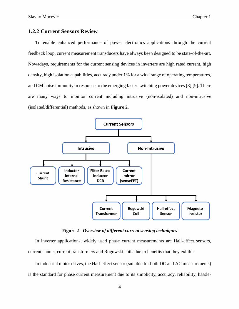
The manufactured GD with PCB-embedded RSCS which is mounted on top of the SiC
MOSFET module is shown on the Figure 22 and Figure 23. Figure 22 shows the top view with
indicated Rogowski coils and current booster stage. Figure 23 shows the bottom view with
indicated power supplies, FPGA, switch current sensor signal processing circuit, GD IC-s and
driving decoupling capacitors.
Slavko Mocevic Chapter 2
37
Figure 22 - Top view of GD prototype
Figure 23 - Bottom view of GD prototype

Slavko Mocevic Chapter 3
38
Chapter 3 Phase Current Reconstruction
and Sensor Performance
3.1 Introduction
Developed GD with integrated RSCS-s have both switch currents measurements. Those pieces
of information can also be used for obtaining the phase current via simple manipulation on the GD
itself. Most important goal for the first version of GD with integrated phase current sensor is to
prove the concept of digital reconstruction under severe noise environment which is created by
SiC MOSFET fast switching. Another important aspects that will try to be achieved are: Linearity
error <2%, Accuracy <2%, < 2μs delay between on board phase current and real phase current in
the system. For EV applications, mentioned delay is tolerable and could possibly be compensated
on the controller level.
3.2 Detailed Block Diagram of Digital Phase Current
Reconstruction
Figure 24 shows more detailed diagram of digital phase current reconstruction with RSCS
measurement. 𝑑𝑖/𝑑𝑡 information, scaled with a factor of mutual inductance, is being constantly
integrated by an active integrator.

Slavko Mocevic Chapter 3
39
Figure 24 - Detailed block diagram of digital phase current reconstruction
The output voltage of an integrator which linearly represents current in the system is filtered
with the 30 MHz high frequency RC filter, after which there is buffering. The purpose of the buffer
is that any manipulation done afterward, does not interfere with the integrator circuit. After buffer,
there is a two-stage ADC filter with a cutoff frequency of 3.3 MHz, the main role of which is to
filter out any high frequency ringing in the current information during switching instances, thus
preventing aliasing in the information. The OpAmp level shifter is employed to adjust the signal
to the proper values for ADC sampling. A high precision 14-bit ADC with ability for over 2 Msps
and 50 MHz serial peripheral interface (SPI) communication clock rate is chosen. The chosen
sample rate is pushed to 2.5 MHz in order to reduce delay of the current measurement. Two ADCs
for top and bottom switch currents are synchronized, and they work in non-stop sampling mode in

Slavko Mocevic Chapter 3
40
order to send sampled data in the FPGA at the same time instances. After data from ADCs is
received, the FPGA performs digital subtraction of data in one clock cycle (10 ns). Immediately
after successful subtraction, FPGA starts placing that information on the DAC SPI bus. A 16-bit,
2.5 Msps, 50 MHz SPI clock rate DAC with small settling time is chosen to convert information
back to analog without creating a lot of additional delay. Since the DAC is a single-channel current
output, an additional external I/V converter OpAmp is employed. This particular OpAmp must
have a sufficiently low offset voltage such that it is not modulated by the DAC output terminal
impedance change. After the I/V OpAmp there is additional level shifter to invert and adjust
current information according to the controller requirements. Another two-stage RC filter with
cutoff frequency of 3.3 MHz is employed to filter out the staircase waveform coming from the
DAC reconstruction process. Based on the previous analysis, the phase current delay can be
expected to be in the range of 1.6 μs, which is shown on the (3-1)
(3-1) 𝑡𝑑𝑙𝑦𝑃ℎ𝑠𝐶 =
𝑡𝑑𝑙𝑦𝑖𝑛𝑡𝑔
+ 𝑡𝑑𝑙𝑦𝑅𝐶 + 𝑡𝑑𝑙𝑦
2𝑠𝑡𝑎𝑔𝑒𝑅𝐶 + 𝑡𝑑𝑙𝑦𝑙𝑣𝑙𝑠ℎ𝑓𝑡
+ 𝑡𝑑𝑙𝑦𝐴𝐷𝐶 + 𝑡𝑑𝑙𝑦
𝐹𝑃𝐺𝐴 + 𝑡𝑑𝑙𝑦𝐷𝐴𝐶 + 𝑡𝑑𝑙𝑦
𝑙𝑣𝑙𝑠ℎ𝑓𝑡+ 𝑡𝑑𝑙𝑦
2𝑠𝑡𝑎𝑔𝑒𝑅𝐶 =
40 𝑛𝑠 + 30 𝑛𝑠 + 300 𝑛𝑠 + 40𝑛𝑠 + 400 𝑛𝑠 + 10 𝑛𝑠 + 400𝑛𝑠 + 40 𝑛𝑠 + 300 𝑛𝑠 =
= 1.56 𝜇𝑠

Slavko Mocevic Chapter 3
41
3.3 Phase Current Sensor Performance
3.3.1 Concept Verification in Double Pulse Test (DPT)
3.3.1.1 Gate Driver and RSCS Functionality Verification
Figure 25 - Simplified schematic of a DPT
A double-pulse signal is sent from the function generator, to the gate drive IC of the bottom
switch. From the dc bus voltage, inductance, and drain current values, the width of the first pulse
needed to achieve the desired current level can be determined. Desired current level is set to be
around 300 A. At the end of this first pulse, the turn off switching waveforms for the device under
test can be captured. In order to obtain the turn on switching waveforms under the same conditions,
a short second pulse is applied. The rising edge of this second pulse gives the turn on switching
waveforms for the device under test. The top switch was kept off with a gate-source voltage of -4
V. The drain-source voltage of the bottom switch was measured with a high-voltage differential
probe from Tektronix, and the drain current was sensed with RSCS after it was fine-tuned both

Slavko Mocevic Chapter 3
42
statically and dynamically. Simplified schematic diagram with indicated measurement is shown in
Figure 25.
The module DPTs revealed fast switching, high slew rates, and ringing and overshoot due to
lowered gate resistance. Waveforms from one of the DPTs conducted on the bottom switch at 600
V and 300 A are shown in Figure 26. All tests were done with external gate resistance of 0.1 Ω
for turn on and 0.05 Ω for turn off in order to push the switching speed.
Figure 26 - Double pulse test waveforms
Figure 26 also shows zoomed in turn-off and turn-on events. Resulting 𝑑𝑣/𝑑𝑡 during turn-off
was around 15V/ns while for the turn on was 11 V/ns. Resulting switching energies were:
𝐸𝑡𝑢𝑟𝑛−𝑜𝑓𝑓 = 7.31 𝑚𝐽, 𝐸𝑡𝑢𝑟𝑛−𝑜𝑛 = 3.82𝑚𝐽.

Slavko Mocevic Chapter 3
43
3.3.1.2 Phase Current Reconstruction Concept Verification
The phase current reconstruction principle will be verified on a 500 V, 300 A double-pulse test
with clamped inductive load. Phase current in this case is inductor current. Results are shown in
Figure 27.
Figure 27 - Double pulse test results and phase (inductor) current delay
Figure 27 clearly shows that the reconstructed phase current waveform (pink) is the result of
subtracting the top switch current (red) from the bottom switch current (blue). Delay between the
reconstructed phase current and the switch current sensed with the commercial Rogowski coil
probe is 1.61 𝜇𝑠, which is ≈100ns higher than the estimated value given in Table 4. However,
this delay corresponds to the delay breakdown analysis done in the previous section. From the
reconstructed phase current waveform, no significant switching noise at the switching transients
can be noticed, meaning that the employed filter values are sufficient, and a possible reduction of

Slavko Mocevic Chapter 3
44
filter frequency to reduce delay, may be applied. A comparison with the commercial Rogowski
current probe in a multiple pulse test on 600 V, 60 kHz is shown in the Figure 28.
Figure 28 - Comparison with the commercial Rogowski current probe
Figure 28 shows that amplitude-wise, the reconstructed phase current measurement (pink)
matches fairly closely with the commercial Rogowski coil current measurement (red) through
whole range, while delay is consistently around 1.6 μs.
3.3.2 RSCS and Phase Current Sensor Error Diagrams
One of the biggest concerns in the applications where Rogowski coil measurement is being
used, is the droop (drift) effect when lower frequency AC or long pulse signals are applied. The
droop effect is a result of the imperfections of the OpAmp integrator circuit, where input offset
error is constantly being integrated together with the incoming 𝑀𝑑𝑖/𝑑𝑡 information, resulting in a
severe output voltage error over longer time periods. This being said it is necessary to evaluate

Slavko Mocevic Chapter 3
45
sensor performance at different switching frequencies (different lengths of on-time). A comparison
is executed between RSCS and the commercial current sensor. Measurements are taken at the end
of the switching interval, since that is where the droop effect is at its most intense. After that,
circuit will reset or disable the output of the integrator, depending of the implementation, and
drooping effect will return back to zero.
Figure 29 shows the relative error of the RSCS (solid line) through the frequencies of pulse
from 1 kHz to 100 kHz, for 50% on-time. Besides that, Figure 29 shows the relative error of the
reconstruction process (dashed line), where reconstructed value is compared with the RSCS at the
end of the switching interval. This comparison is done in order to determine how much the
reconstruction process is making errors. All measurements are taken at room temperature, since
this GD is made to validate the reconstruction principle in environments with high CM noise.
Figure 29 - Resulting error diagram

Slavko Mocevic Chapter 3
46
Figure 29 shows that high current relative error (considering RSCS comparison with
commercial sensor) is low and is around 1% for frequencies higher than 10 kHz. Absolute error,
considering high current, is than a maximum of 3A. Low current relative error is approximately
4% for frequencies higher than 10 kHz. Absolute error considering this case is again smaller than
3A. However, when switching frequency is reduced bellow 10 kHz, relative error starts ascending
enormously due to severe integration error of the integrator OpAmp for both low and high currents.
The previous results turned out to be promising for power modules with intended switching
frequencies above 10 kHz, which are within the SiC MOSFET domain. Reconstruction error
(reconstructed phase current with respect to the output of the RSCS) ranges from 0.5 – 3% for all
considered switching frequencies in a high current case. Low currents have a slightly higher
relative error, ranging from 6 – 8.4%. Even though this relative error seems large, in absolute
values it is smaller than 3 A for a 30 A current. As expected, compared reconstruction error does
not depend on switching frequency. However, there is definite room for improvement of these
results since better OpAmps, ADCs, DACs as well as faster SPI bus speed and sampling time
could be implemented.
3.4 Phase Current Sensor Performance in Inverter
Applications
3.4.1 Phase Current Sensor Performance in Continuous PWM Inverter
3.4.1.1 Experimental Setup and Modulation
The experimental inverter test setup is shown in Figure 30. Three of the developed GDs with
phase current sensors are connected to the 1.2 kV, 300 A SiC MOSFET module. The inverter is
mounted on the water-cooled cold plate to avoid overheating during continuous testing. Inverter
DC voltage was set to be 600 V. Used source was Magna Power, 100 kW max, 1 kV max. The

Slavko Mocevic Chapter 3
47
load is consisted of a 0.27 mH three phase inductor together with a water-cooled 1.7 Ω resistor in
each phase. Modulation used to control inverter is open loop sinusoidal PWM (SPWM), due to
implementation simplicity. Modulation index is set to be around 0.9. Dead-time in this case, since
turn-on and turn-off time of the switches is very fast (<100ns), is set to be 300 ns. The switching
frequency is set to be 30 kHz, while modulation (line) frequency is 400 Hz.
Figure 30 - Experimental inverter test setup

Slavko Mocevic Chapter 3
48
3.4.1.2 Experimental Results
Figure 31 shows the reconstructed current from one of the phases, together with the switches’
current in the corresponding phase, alongside with the corresponding phase voltage. It is easily
observable that on-board phase current is result of subtraction of the same phase switches currents.
Figure 31 - Reconstructed phase current of the inverter phase
As seen before in Figure 28, Figure 31 clearly shows the reconstructed phase current
waveform (blue) is the result of subtracting top switch current (red) from the bottom switch current
(green), now for the inverter case. Purple waveform is representing line-to-line voltage. Figure 32
shows comparison with the commercial measurement (green). The delay is still consistent and its
value is 1.6 μ. The reconstructed phase current follows the commercial measurement very well in
both amplitude and phase with predetermined delay. These tests are performed with the very low
gate source external resistance (𝑅𝐺𝑆𝑜𝑛 = 0.1 𝛺, 𝑅𝐺𝑆
𝑜𝑓𝑓= 0.05 𝛺) in order to push the transient speed

Slavko Mocevic Chapter 3
49
and reduce switching losses. The 𝑑𝑣/𝑑𝑡 in this case was 15 𝑉/𝑛𝑠, which cannot be pushed much
more due to large internal gate resistance of 3 Ω. In this noisy environment, the switch currents in
Figure 32 show that there are no shoot-through events caused by either the Miller effect or induced
signal malfunction. Furthermore, the components chosen to participate in phase current
reconstruction cope well with the CM noise created by the 𝑑𝑣/𝑑𝑡, and successfully reconstruct the
phase current.
Figure 32 - Comparison with the commercial phase current measurement
Figure 33 presents a spectral comparison of on board phase current sensor with 2 commercial
phase current sensors, Rogowski (from PEM) and Hall-effect sensor (from LEM). As it can be
seen, on board phase current sensor contains more noise than both of commercial measurement
which can be expected. On board phase current sensor is located on GD board on the path of the

Slavko Mocevic Chapter 3
50
common mode current coming from the device switching. Even though different mitigation
techniques were employed to minimize that noise, not all of it could be suppressed. This noisier
part is observable on the multiple of switching instances (30 kHz, 60 kHz etc.) where blue (on
board sensor) results in higher peaks than commercial measurements. One more important part
that can be also noticed from frequency spectrum is that between 400 Hz and 30 kHz there is no
significant harmonics in the spectra, which is expected and experimentally verified. Most of
spectral energy is located on the 400 Hz, which is the modulation frequency used.
Figure 33 - Frequency spectra of the 3 different phase current measurement techniques
3.4.1.3 Linearity Error
Since accuracy of the sensor has already been assessed in the previous subchapter, linearity
error (non-linearity) will now be explored as it is one of the crucial aspects of analog current
sensors. Due to the analog output of the phase current sensor, linearity is very important in order
to have correct measurement. Even though the Rogowski coil is linear element without possibility
of reaching saturation (basically air core, since FR4 is not ferromagnetic material), the integrator

Slavko Mocevic Chapter 3
51
OpAmp, buffer stages ADC, FPGA or DAC may influence linearity and result in a non-linear
transfer function between phase current and analog voltage information that represents it. The
linearity error of the transducer is an expression of the extent to which the actual measured curve
of a sensor departs from the ideal curve. Based on the definition given in [8], the linearity is the
maximum positive or negative discrepancy with the reference straight line (ideal curve), expressed
in the full scale of measured current. That definition translates to the next equation:
(3-2) 𝐿𝑖𝑛𝑒𝑎𝑟𝑖𝑡𝑦 𝑒𝑟𝑟𝑜𝑟 (%) =𝛥𝑉 (𝑉)
𝐼𝑝𝑚𝑎𝑥 (𝐴)∙𝐺(𝛺)
The mentioned straight line (ideal curve) is defined based on the sensitivity of the sensor.
Sensitivity of the phase current sensor is set to be:
(3-3) 𝐺(𝛺) =𝑉𝑜𝑢𝑡(𝑉)
𝐼𝑝ℎ𝑠(𝐴)=
1.2 𝑉
60 𝐴= 0.02 𝛺
Figure 34 shows the experimental results for linearity error, where the blue line represents the
ideal case reference line based on defined sensitivity. The black lines represents bounds of
maximum positive and negative error. Output voltages are measured for a range of currents from
-165÷165 A, and for the reference current, a commercial Hall-effect sensor measurement is taken
under the assumption that it is perfectly linear. Figure 34 shows that the maximum discrepancy of
output voltage from the reference line is 0.084V. Based on the given equation, linearity error is
2.5%. This outcome could have been somewhat expected based on the results of the accuracy
measurement in previous subchapter and from the performance observed in Figure 29. Linearity
error is somewhat larger than anticipated, however this can be significantly improved in the next
versions of the GD with integrated current measurements.

Slavko Mocevic Chapter 3
52
Figure 34 - Linearity error of the phase current sensor
3.4.2 Phase Current Sensor Performance in Discontinuous PWM Inverter
3.4.2.1 Sensor Problem during Discontinuous PWM
Active integration circuit using OpAmp is selected to achieve wider sensor bandwidth and
extract correct current waveform from information coming from the Rogowski coil. Reset switch
is added to the integrator to reset the output to zero when the SiC MOSFET is switched off, to
resolve the problem of an input offset of OpAmp being constantly integrated and invalidating the
output of the sensor. In continuous pulse width modulated systems sensors will work almost
perfectly for switching frequencies above 10 kHz (Figure 29). However, when there is a PWM
signal that is longer than 100𝜇𝑠, developed sensor starts being inaccurate and invalidates the senor
output since integration error becomes severe. For discontinuous PWM (DPWM), during clamped

Slavko Mocevic Chapter 3
53
period there is no reset signal (not in this version), thus making the measurement invalid. Figure
35 shows typical RSCS and phase current sensor behavior during DPWM in inverter application.
Figure 35 - Behavior of sensors during DPWM
It can be seen that as long as there is a continuous PWM pulse train, reset sensor will work and
sensor output will match real currents in the system. When the DPWM starts, correct waveform
will be observable for few switching cycles (depending on switching frequency). After few
switching cycles pass, on board current measurement starts to depart more and more from the real
one. Since there is no reset signal coming from the FPGA, measurement will drift more and more.
Controller cannot anymore relay on the measurement coming from board during this period. In
one of the following subchapter this will be experimentally confirmed for VSI case, and solution
for this problem will be proposed due to a fact that DPWM schemes are often used in automotive
applications to reduce losses in the system and increase effective voltage when needed.

Slavko Mocevic Chapter 3
54
3.4.2.2 Experimental Setup and Modulation
Experimental setup remained same as described for Continuous PWM, shown in Figure 30.
Switching frequency remained the same as previous, 30 kHz, while the line frequency is changed
to 100 Hz for better observation of sensor performance in the clamped period of DPWM. Chosen
DPWM modulation scheme is carrier-based conventional 60𝑜 DPWM, further described in the
[46], [47]. This modulation scheme is chosen due to simplicity since it is using unchanged
sinusoidal reference waveforms from continuous PWM. Fundamentals of this modulation are
shown on the Figure 36. Basically, zero sequence (green waveform) is added to phase voltages
such that resulting waveform is DPWM signal (red waveform). This zero sequence will not be
observed on the line-to-line voltages based on the symmetrical and balanced three phase theory.
Figure 36 - Conventional 60 degrees DPWM
Slavko Mocevic Chapter 3
55
3.4.2.3 Experimental Results
Experimental results for DPWM scheme are shown on the Figure 37.
Figure 37 - DPWM scheme phase current waveforms
Figure 37 confirms that whenever there is a clamped period in one of the phase voltage, phase
current measurement coming from the corresponding gate driver will be incorrect due to RSCS
drifting related problem previously described. Closed loop current control cannot be realized based
on this current measurement since periods of severe inaccuracy exist, and online compensation is
unfortunately impossible. However, this problem could possibly be overcome on the controller
level. According to fundamentals, while one phase is clamped, other two will be switching. Since
the 3phase VSI motor control is intended application of these gate drivers, sum of currents in each
instance will be zero, as shown in the (3-4)

Slavko Mocevic Chapter 3
56
(3-4) 𝑖𝑎 + 𝑖𝑏 + 𝑖𝑐 = 0
Basically, this means that current in one of the phases can be calculated as the negative sum of the
currents in the two other phases. Based on that, whenever one phase is clamped, current in that
phase can be extracted from other two phases on the controller side. Fact that other two phases are
switching, results in valid current measurement in the switched phases, and thus the reconstructed
value. This makes on board phase current sensor valid for both continuous and discontinuous
PWM schemes. Figure 38 shows reconstruction principle idea for phase C, where green is the
actual current waveform coming from phase C gate driver. Red waveform is the one created by
negative sum of the other two phase currents in the system, while blue is the real current in the
system which could be obtained by adding them together.
Figure 38 - Sensor during DPWM reconstruction principle

Slavko Mocevic Chapter 3
57
Simplest way to verify this approach would be analog way on the scope, since scope has neat
math function options. This can be done before any controller software code implementation is
done in order to obtain valid current measurement results during DPWM. Experimental
verification can be seen on Figure 39, where yellow (on board phase C) waveform alongside with
orange (waveform calculated from other 2 phases) are located directly on top of the measurement
taken with commercial Hall-effect sensor placed on phase C.
Figure 39 – Analog DPWM current reconstruction verification
3.4.2.4 Proposed software solution for DPWM schemes
Based on the Figure 38 and Figure 39, simple algorithm on the controller has to be
implemented in order to overcome incorrect current problem and get correct current values during
whole line cycle during DPWM scheme. Piece of code implemented in the microcontroller

Slavko Mocevic Chapter 3
58
interrupt routine for phase C current, right after controller reads from ADC terminals is shown on
Figure 40.
Figure 40 - Current reconstruction algorithm for phase C
Current waveforms are constantly sampled. Based on the simple DPWM duty cycle reference,
it can be decided which current for corresponding phase to be used. If duty cycle is clamped to
either 0 or 1, reconstructed current (negative sum of other two phases) value will be used. If duty
cycle reference is not clamped, current coming from corresponding GD board is correct and can
be used for closed loop current control. Some delays were inserted in the transition periods, from
clamped to switching part of DPWM and vice versa, in order for the RSCS to reset and catch up
with correct values. These delays are completely justified since system can rely on the currents
coming from the phase for a few switching cycles when there is no reset signal according to the
Figure 29 on 30 kHz. Reconstruction algorithm can be verified, since online register monitoring
of controller is possible. Right side of Figure 41 shows register where 𝐼𝑎, 𝐼𝑏, and 𝐼𝑐 values are

Slavko Mocevic Chapter 3
59
shown after reconstruction algorithm is employed, while left side shows original measured
waveforms sampled by controller.
Figure 41 - Values of reconstructed currents stored in controller registers
3.5 Influence of Adjacent Phases on Rogowski Coils
Due to a fact that all of Rogowski coils are located on the controller ground on different GDs,
electrical influence between phases on Rogowski coil measurement is expected and will be
investigated. Proximity magnetic field influence in error of Rogowski coil measurement is also
investigated since inverter phase-legs are placed close together and DC busbar is on top of all of
them.
3.5.1 Electrical Influence
Controller ground on GD, contains CM noise coming from different device switching in the
three phase system. Since different phases will have different switching events, influence on
Rogowski coil measurement of adjacent phases is expected.

Slavko Mocevic Chapter 3
60
Output of the Rogowski coil will be investigated on one of the phases since that information
will later on being integrated by the OpAmp integrator. Circuit used to investigate both cases is
shown on the left part of the Figure 42, while inverter is shown on the right side of the figure.
Used modulation was simple sinusoidal open loop PWM modulation for full bridge. Modulation
frequency is set to be 𝑓𝑚 = 400 𝐻𝑧 with carrier frequency (PWM frequency) set to be 𝑓𝑠𝑤 =
35 𝑘𝐻𝑧. In the case of electrical influence of the adjacent phases, phase B is powered on and
connected to the busbar. Power comes from the same power supply that powers two other phases,
and their common ground is thus same. Both switches of phase B are however turned off by
controller and not switching in order to observe influence from other phases.
Figure 42 – Schematic and hardware for influence investigation
Results that are shown on Figure 43 are measured at Rogowski coil output of the phase that is
not switching (phase B). Ideally, this output should be clamped at 0 V. Due to electric coupling on
common ground that lies on the path of common mode noise, this will be picking up noise. From
Figure 43 can be seen that some amount of the noise can be seen on the output of Rogowski coil.
Looking at the figure it is not known whether this noise is purely electric coupled noise, or there
is magnetic coupling noise. However, after observing results from next subchapter, it can be
concluded that this is mostly electrical noise. Spectral analysis is shown on the Figure 44.

Slavko Mocevic Chapter 3
61
Figure 43 - Experimental results from electric influence of adjacent phases
Figure 44 - Spectrum of bottom Rogowski coil output in phase B
As it can be assumed and observed from Figure 44, significant amount of noise can be
observed the multiples of switching frequency. Due to the fact that that noise is at least 55dB
smaller than the actual Rogowski coil output that measures FB current, it can be concluded that

Slavko Mocevic Chapter 3
62
this influence is negligible. Most important fact is that there is basically no influence on the lower
frequencies such as modulation frequency.
3.5.2 Magnetic Influence
The Rogowski coil sensor measures the current through it. However, there is a possibility of
induced voltage from variable magnetic field created by the current from other 2 phases in the
inverter application. The magnetic field created by currents in the other two phases or busbar
becomes disturbance magnetic field. This disturbance magnetic field passes through coil section
of the Rogowski coil with magnetic field created by measured current and induces corresponding
disturbance voltage. The disturbance voltage is superimposed on ideal measurement signals, which
could produces error to the measurement result if the influence is significant. Therefore, this
magnetic influence has to be investigated.
Circuit used to investigate is shown on the Figure 42, and it remained essentially the same as
for electrical influence. In this case middle gate driver is disconnected from power supply as well
as from the busbar. However, this disconnected gate driver with Rogowski coils is left bellow the
busbar in order for us to see is there any magnetic influence coming from adjacent phases and
busbar itself. Same experimental setup as before (Figure 42) is used with same modulation
frequency as well as the same switching frequency of full bridge inverter.
Results that are shown on Figure 45 are measured at Rogowski coil output of the phase that is
not switching (phase B). Ideally, this output should be clamped at 0 V. Due to coupling this will
be picking up noise. It can be seen that some amount of the noise can be seen on the output of
Rogowski coil. Looking at the figure it is not known whether this noise is purely magnetic coupled
noise, or this is noise picked up by probe However, after observing these results it can be concluded

Slavko Mocevic Chapter 3
63
that the noise from previous subchapter is electrical since magnitude of the noise in that case was
much higher.
Figure 45 - Experimental results from magnetic influence of adjacent phases
Figure 46 shows spectral analysis results where blue waveform is output of Rogowski coil in
normal operation in on one of the switched gate drivers and enabled current sensing. Red waveform
represents input to the Rogowski coil of the gate driver that is disconnected from the setup. As it
can be seen, red waveform is significantly smaller (40dB – 100times) than the blue waveform.
That means that either magnetic coupling is significant, only 100 times smaller than one expected
in normal operation or the probe is picking up radiated switching noise that is present around
experimental setup. In that sense more experiments are conducted. Now probe itself is left lying

Slavko Mocevic Chapter 3
64
next to the busbar with connected tip to the ground of the probe via very short wire. In this manner,
it will be established is most of the noise picked up by the probe, or is the magnetic influence
indeed that strong on switching frequency and their multiples.
Figure 46 – Spectral analysis results for magnetic influence
Figure 47 shows spectral analysis results where blue waveform is output of Rogowski coil in
normal operation in on one of the switched gate drivers and enabled current sensing. Red waveform
represents input to the Rogowski coil of the gate driver that is disconnected from the setup. Yellow
waveform presents results of the probe alone sitting close to the DC bus with shorted probe tip to
the GND of the probe. Passive probes are used for measuring in each case. It can be seen that
yellow waveform is almost the same as the red one. There is very small difference in between
these two waveforms. This means that most of the coupling effect measured in the previous case
were picked up by the probe itself and did not have to do with the actual output of the Rogowski
coil. This means that magnetic coupling between adjacent legs is very small, almost negligible.

Slavko Mocevic Chapter 3
65
Figure 47 - Spectral analysis results for magnetic influence with environmental noise results
Therefore:
Electrical influence of switching noise from one phase leg to other exists. Reason for
this lies in the fact that current sensor circuit of the inverter are on the common ground
(controller ground) which inevitably lies on the noise path
There is no influence on the fundamental frequencies for any of the measurements
which is very important in order for controller not to contain low frequency harmonics
For magnetic influence experiments it can be concluded that most of the noise is picked
up by the probe
It appears that there exists small magnetic coupling between busbar and Rogowski coil
even when the phase leg is disconnected. However that influence is negligible.

Slavko Mocevic Chapter 4
66
Chapter 4 Short-Circuit protection
performance
4.1 Introduction
SC protection is one of the most critical functionalities of the GD that prevents semiconductors
from breakdown. Since SiC MOSFET power module package usually has small internal
inductance, small on state resistance, and “soft” output characteristics, fast SC current 𝑑𝑖/𝑑𝑡 will
cause the current to rise fast to a high level causing possible destruction of the module due to
excessive dissipated energy or high overshoot during the turn-off. Therefore, response time is very
critical for the SC protection of SiC MOSFETs due to the limited SC withstand time [39].
Whichever detection method and protection mechanism is used, its implementation need to have:
• Fast detection and reaction impacting the current peak, limiting the overheating, stresses
• Responsive for all SC types and not degrade conduction or switching characteristics
• Turn-off in a safe manner
• Easy implementation in any GD design
• Robust and high noise immunity
Introduced high sensing range, high bandwidth, low response delay, high noise immunity and
high accuracy RSCS as a detection method together with the protection mechanism of the
implemented Driver IC in the Chapter 2 fulfils all those characteristics.

Slavko Mocevic Chapter 4
67
4.2 Types and Behavior of Short-Circuit in the Half-Bridge
Configuration
In the half-bridge configuration, 2 types of SC exist. Figure 48 shows that one type of fault is
referred to as shoot-through, while the other is referred to as SC at the load, OC event, or simply
load fault. Focus is set on the bottom switch (Q2) in the half-bridge.
Figure 48 - Types of SC in the half-bridge configuration
4.2.1 Shoot-through Type of Short-Circuit
In case of a transistor or diode destruction, failure in the controller or signal transmitters, due
to noise induced malfunction of the switch-on and switch-off signals, conduction time of both
switches in half bridge configuration may overlap, leading to a shoot-through event. Depending
on conditions at what shoot-through occurred two cases exist. The first case is called “Fault Under
Load” (FUL) and the second is “Hard Switching Fault” (HSF) [34], [35], [36], [38], [48], [49].
FUL:
FUL is a type of fault that occurs when the device is on and conducting. Referring to Figure
48, initially device Q2 is gated on and it is carrying steady current within its ratings. Therefore,
voltage across device 𝑉𝑑𝑠𝑄2
is low. Fault in the system is created by the turning on of the

Slavko Mocevic Chapter 4
68
complementary switch, in this case Q1, thus causing the shoot-through event. Due to a very low
stray inductance in the current path, current rise (𝑑𝑖/𝑑𝑡) in this case is severe.
HSF:
HSF fault occurs when the device channel is not opened, and the device is directly gated on
into the fault. The inductive load from Figure 48 is shorted by the switch Q1 being on. Switch Q2
is off, meaning that device is holding full system dc link voltage. Fault is imposed to the system
when Q2 switched on. Upon application of the gate signal to the Q2 and following gate-source
voltage reaching gate threshold voltage, current begins to rise. Similar as in FUL case, very low
stray inductance will cause a rapid current rise.
4.2.2 Load Fault Type of Short-Circuit
Due to an incorrect wiring, dielectric breakdown of load, short-circuit of the windings of an
induction motor, ground fault etc. load fault type of short-circuit may occur (Figure 48) [49]. In
this case, inductance of the load wire, motor cable or the rest inductance of the motor windings
plays a significant part in the behavior of the SC. Current slope is determined by the that
inductance. Therefore, location of the where the short-circuit happens occurs, is of great
importance, because it will determine fault inductance and hence, current slope. There will be high
current slope and higher stress to device when the SC happens near the module terminals and
slower current slope and lower stress when the SC happens on the motor winding. This type of SC
is less stressful to device than the shoot-through types, often called OC event.
4.2.3 Behavior during Short-Circuit Event
In order to observe behavior of current, gate-source, and drain-source voltage and to define
important aspects of SC protection, an unprotected SC event is created in the system (load fault
with SC very close to the half bridge terminals).

Slavko Mocevic Chapter 4
69
Typical experimental waveforms of such SC can be observed in Figure 49. SC gate signal is
limited to be 2.2 𝜇𝑠, while the dc link voltage is 𝑉𝑑𝑐 = 400𝑉.
Figure 49 - Experimental waveforms in short-circuit without protection
Four distinctive phases can be identified. In phase A, current starts to rise due to applied gate
signal. Current rise (𝑑𝑖/𝑑𝑡) is dictated by the inductance in the path (stray inductance of the
module and additional inductance of the load wire), transistor characteristic (threshold voltage and
transconductance), gate driver parameters (gate resistor and applied 𝑉𝐺𝑆 voltage) and dc link
voltage. Voltage over the device drops to a lower value, and that value is determined by voltage
drop over 𝑅𝐷𝑆𝑜𝑛 and 𝐿𝑠𝑡𝑟𝑎𝑦𝑑𝑖
𝑑𝑡. According to the Figure 49, at the beginning 𝑑𝑖/𝑑𝑡 was
approximately 5𝐴/𝑛𝑠, which implies that current rises very fast and can reach peak values shortly
after applied gate signal which can be destructive due to excessive dissipated energy and thus heat.
Therefore, protection detection and reaction times are crucial. Phase B starts when current reaches
a level where SiC MOSFET starts its transfer from the ohmic region to the saturation region and
voltage over the SiC MOSFET device builds to the dc link voltage value. At the beginning of

Slavko Mocevic Chapter 4
70
Phase C, due to an increase of resistance in the module when dissipated energy is heating the
module, current will drop off from its peak value. Following that drop, the device is exposed to
both high current and high voltage. If the protection still did not react before entering this phase,
it is crucial for protection to react as fast as possible as now energy dissipation and thus heat is
tremendous, and withstand time of SiC device is not as long as the IGBT device, so thermal
runaway may occur. Start of the Phase D occurs when the gate signal goes low, and the SiC device
is turned off. Due to 𝑑𝑖/𝑑𝑡 of the decaying current and inductance in the system, 𝑉𝐷𝑆 voltage will
rise significantly over the parasitic inductances threatening to destroy the device due to
overvoltage. Figure 49 indicates that voltage overshoot in this case is more than 800V, which
gives more than 1.2 kV voltage across device. Since this is rated voltage and testing is done on
400V, it can be expected that on higher dc bus voltages, voltage across the device is even higher
and possible destruction due overvoltage may occur. Therefore, it is recommended when shutting
off the overcurrent that the device be turned off gently. Method to turn of device in a safe manner
is STO – 2LTO, whose functionality and design will be described in one of the next subchapters.
According to the behavior of the device during the short-circuit and all of previously stated,
performance of the SC detection and protection method can be evaluated via next segments:
A. Time spent in SC (time from beginning to the end of SC) [𝜇𝑠] – should be as short as
possible to minimize the energy dissipation during SC since current and voltage are high
B. Detection time (time from beginning to the detection – creation of fault signal) [𝑛𝑠] –
should be as short as possible to minimize current peak, voltage overshoots and thus
dissipated energy
C. Reaction time (time from the detection until 2LTO is initiated) [𝑛𝑠] – should be as short as
possible to reduce current peak, voltage overshoots and thus dissipated energy

Slavko Mocevic Chapter 4
71
D. Energy dissipated on devices during SC (maximum dissipated energy in module or devices
– product of voltage, current and short-circuit time) [𝐽] – should be as small as possible in
order not to reach breakdown energy of the module so destruction (thermal runaway, gate
breakdown failure etc.) does not occur
E. Current peak (maximum current during shortcurcuit) [𝑘𝐴] – should be as small as possible
to reduce dissipated energy and large overshoots due to descending 𝑑𝑖/𝑑𝑡 during turn-off
F. Voltage overshoot (maximum overshoot measured on both devices in half-bridge) [𝑉] –
should be as small as possible in order to reduce possibility of exceeding breakdown
voltage and triggering avalanche event and possible destruction of the device
4.3 Detection and Protection Mechanism
Protection mechanism is shown on the Figure 50.
Figure 50 - Rogowski switch current sensor protection mechanism

Slavko Mocevic Chapter 4
72
The switch current sensor is composed by a Rogowski coil and a signal processing circuit
which mostly comprises of integrator and reset. The Rogowski coil generates 𝑑𝑖/𝑑𝑡 value of the
sensed current scaled by a factor of the mutual inductance. The integrator is employed with the
coil to convert the 𝑑𝑖/𝑑𝑡 information back to the current information. In reality an ideal integrator
does not exist, so error of integration must be eliminated in order to sense correct values of the
switch current. To resolve the problem, an active reset switch is added to the integrator to reset the
output to zero when the SiC MOSFET is switched off. Eventually the switch current sensor can
sense pulsating current with correct amplitude. High bandwidth sensed current waveform is then
being sent to the comparator. This value of current is then being compared with the value that is
set to be indicator of SC. In this case, voltage source is set to correspond to a 600A, which is the
2 times higher value than the rated one in the module. This value is chosen in order to avoid current
peaks detecting SC during the turn-on of the device, which can be up to 1.8 times rated current at
both high and low temperature. Therefore, whenever there is current higher than 600A in the
system, the comparator will generate a fault signal. Fault signal is then transmitted through the
digital isolator to the isolated side of GD in order to trigger the protection. Sense pin of the GD IC
on the isolated side in this case serves as a SC and OC indicator. The original purpose of the sense
pin is OC protection in the systems with IGBTs that have phase current measurement [50], but as
mentioned, this pin in this particular GD, is utilized to serve as a SC/OC indicator. When fault
signal (logical ‘1’) is brought to this pin, GD will initiate 2LTO after 200ns of processing time,
and system will be shut down in a safe manner. This behavior is under assumption that OpAmp
integrator is not previously saturated and showing correct current values.
SC performance during DPWM modulation will be shown in the Appendix A, since this case
can present possible problem due to imperfections of the OpAmp and possible saturation.

Slavko Mocevic Chapter 4
73
4.4 Two-level Turn-off (2LTO) Design
4.4.1 Background
The turn-off current will be extremely high when the SC protection is triggered, and a hard
turn-off will possibly destroy the device due to the induced turn-off voltage spike. Therefore, either
a soft turn-off process or a VDS clamp circuit by using TVS diode is necessary for the SC turn-off.
The STO is selected because in the latter approach the breakdown voltage of TVS varies in a wide
range such that the VDS clamp voltage is difficult to control. A STO functionality is usually
combined together with SC protection, although in some cases STO is employed even in normal
operation to reduce voltage overshoot during turn-off in systems with excessive voltage spikes
during switching events. In this GD, STO functionality is employed only with the SC protection.
In state-of-art designs, two typical STO mechanism are adopted by different driver ICs
manufacturers. One is to increase the turn-off resistance hundreds times higher than normal when
soft turn-off is triggered (Also called large resistance turn off - LRTO), while the other is to use
2LTO voltages. The first approach does not apply to the designs where an external gate current
booster is required since recommended method is increasing the input capacitance of the current
booster which is unfortunately undesirable for high frequency applications, since the normal
switching process will also be delayed by hundreds of nanoseconds. Therefore, selected GD IC is
one with the 2LTO technique.
The transfer characteristics (𝐼𝐷 vs. 𝑉𝑔𝑠 ) of the MOSFET determines how the gate voltage
controls the drain current. The intermediate voltage level in 2LTO (2LTO voltage) should be
ideally designed corresponding to the peak normal-operation current according to the transfer
characteristics, as the normal turn-off is allowed at this peak current and would not definitely cause
overshoot above rated voltage if designed well. The duration of this intermediate voltage level

Slavko Mocevic Chapter 4
74
should be long enough for the drain current drops to the peak normal-operation current. However,
the datasheet only give the transfer characteristics at one drain-source voltage, where in practical
applications the drain-source voltage varies as well as the drain current during the turn-off process.
Also, if the peak current in SC is much higher than the normal-operation current, first voltage
overshoot due to large 𝑑𝑖/𝑑𝑡 can cause significant overshoot that exceeds rated voltage of the
device and threatens to destroy it. Furthermore, time spent in 2LTO voltage (2LTO time) should
be short enough for the device not to reach breakdown energy. Energy dissipated during 2LTO
can be excessive due to a fact that voltage is at the DC bus value and current is close to the rated
current. Taking all of the previously mentioned into the account, it is very difficult to pre-calculate
the proper design value, and thus the better way to determine the intermediate gate voltage by tests
varying 2LTO voltage and time in order to find the best and most suitable option.
4.4.2 Design Goals and Terminology
Goal of these tests is to find a most suitable 2LTO performance (both 2LTO voltage and time)
that will not result in excessive voltage overshoot during SC turn off, as well as not reaching the
breakdown energy of device (for CAS300M12BM2 breakdown energy is 6.9J [32] ).
Now, proper terminology will be introduced so design objectives could be defined. Figure 51
shows one SC event, load fault with very small inductance (short happened close to the device
terminals). Detection and protection mechanism used in this case was described RSCS protection
mechanism.

Slavko Mocevic Chapter 4
75
Figure 51 – 2LTO test waveform to introduce terminology
Figure 51 defines most important factors in determining what 2LTO voltage and 2LTO time
should be used in protecting device. These factors are: 1st voltage peak, 2nd voltage peak, peak
current, saturation current and energy dissipated during 2LTO. Behavior in this figure is really
simple: once short-circuit is detected, GD initiates 2LTO which limits the current according to
transfer characteristic of the device. Drop in the current results in the 1st overshoot event, while
cutting of the current that is limited by the transfer characteristic of the device (saturation current)
will result in 2nd voltage overshoot.
Design objectives in this case are:
1st voltage peak should not exceed rated voltage for none of the SC events – 1.2 kV
voltage should not be exceeded
2nd voltage peak should not exceed rated voltage for none of the SC events – 1.2 kV
voltage should not be exceeded

Slavko Mocevic Chapter 4
76
Enough margin should be left for both voltage peeks not to reach rated voltage – voltage
margin of 10% (~100V) will be left
Energy contributed by 2LTO should be as small as possible to avoid destruction of
device – device cannot reach 6.9J energy otherwise it will be destroyed
Time spent in 2LTO should be as small as possible, but long enough to successfully
reach 2LTO voltage and for the drain current to drop to the corresponding saturation
value.
To be able to change 2LTO voltage and time, proper register in STGAP1S needs to be changed,
since this GD is programmable. There is possibility of changing the 2LTO voltage from 7 to 14.5V
and 2LTO time from 0.75 μs to 5.5 μs. Since SiC devices are much faster than IGBT ones, 2LTO
times that will be tested are: 0.75, 1, 1.5, 2, 2.5, and 3 μs, while 2LTO voltages that will be tested
are: 7, 7.5, 8, 8.5, 9, 9.5, 10, and 10.5 V.
4.4.3 Experimental Results and Conclusion
First, 1st voltage overshoots and 2nd voltage overshoots behavior with different voltages and
times will be compared on the Figure 52. Second, energy dissipated in 2LTO events with different
2LTO voltages and times will be compared. Current peak during SC is not dependent on the 2LTO
option, it is dependent of reaction and detection time of protection so that aspect will not be
compared.

Slavko Mocevic Chapter 4
77
Figure 52 - Behavior of 1st and 2nd voltage overshoot with varied 2LTO voltage and time
Based on the results presented in the Figure 52, 1st voltage peek is getting lower as we increase
2LTO voltage, because the difference between current peak and saturation current is getting lower.
Difference between current peak and saturation current is getting lower due to a fact that by
increased 2LTO voltage, according to the transfer characteristics of device, saturation current is
getting higher. Therefore, smaller difference will result in smaller 𝑑𝑖/𝑑𝑡 which will ultimately
result in smaller induced voltage on the parasitic inductances (smaller overshoot). Furthermore,
for same 2LTO voltage, 1st voltage peek is kind of constant and not dependent of 2LTO time since
it mostly depends on current peak, which is being determined by protection detection and reaction
time among other things. As far as the 2nd voltage peak is concerned it can be seen that is getting
higher as we increase 2LTO voltage, because saturation current is getting higher due to lower
resistance of the channel. Figure 52 indicates also that 2nd voltage peek is pretty much constant
and not dependent of 2LTO time, it mostly depends on the saturation current level. However, there

Slavko Mocevic Chapter 4
78
is a slow, but noticeable, decay in the 2nd voltage overshoot with time. This can be explained
through the fact that as the time spent in SC becomes longer, energy dissipated is higher thus
making junction temperature higher too. Since the temperature is increasing, resistance of the
channel is also increasing, thus limiting current to the lower values. Also, one slight contributor
for this could be slight dc bus capacitor discharge.
Figure 53 - Dissipated energy contributed by 2LTO with varied 2LTO voltage and time
Figure 53 indicates that as 2LTO voltage is being increased, energy dissipated in the system
during 2LTO is also increasing. This is due to increase of saturation current. Since dc bus voltage
during this period is approximately at dc bus level (device is saturated), dissipated energy will
clearly be higher. Furthermore, that dissipated energy during 2LTO is increasing linearly with the
time for specific 2LTO voltage (current and voltage roughly remain same during 2LTO). Total
dissipated energy for all these cases was smaller than the breakdown energy of the module. Only
difference between total energy dissipated and energy dissipation contributed by 2LTO mechanism

Slavko Mocevic Chapter 4
79
is roughly constant through all cases, and it is around 400-450 mJ. This is due to somewhat
constant peak current through all SC tests since detection and reaction times were constant.
Based on the results shown on the Figure 52 and Figure 53, it can be concluded that 2LTO
time does not have significant influence on overshoots and that with longer time dissipated energy
is getting higher in the power semiconductor devices. Even though 2nd voltage peak is getting
somewhat smaller, since energy in the system is getting significantly higher with longer time,
chosen 2LTO time is 750ns (as short as possible for this GD IC). SiC devices are fast in transitions
and there is no reason to hold it in saturation for longer time than 750ns dissipating energy.
In order to finalize which 2LTO voltage will be used, maximum voltage peak will be compared
with the dissipated energy during 2LTO. Maximum voltage peak is chosen between 1st and 2nd
voltage overshoot for different 2LTO voltages, for same 2LTO time (750ns). This comparison is
shown Figure 54.
Figure 54 - Comparison between maximum voltage peaks and dissipated energy

Slavko Mocevic Chapter 4
80
Figure 54 shows that there are 4 possible cases in which max overshoot does not reach 1100V,
which is the value that is chosen as the maximum one that can exist in the system. For these cases
dissipated energy is not significant. These points are: [540 mJ (942 mJ), 1060 V] for 𝑉𝐺𝑆 = 7 𝑉,
[570 mJ (977 mJ), 1030 V] for 𝑉𝐺𝑆 = 7.5 𝑉, [630 mJ (1033 mJ), 1030 V] for 𝑉𝐺𝑆 = 8 𝑉, and [700
mJ (1100 mJ), 1050 V] for 𝑉𝐺𝑆 = 8.5𝑉, where value in bracket is total dissipated energy. Any of
these 4 points could be chosen. Main criteria for deciding what point should be chosen (and thus
the corresponding 2LTO voltage) is minimum dissipated energy. Therefore, point [540 mJ (942
mJ), 1060 V] is chosen as a design reference. Corresponding 2LTO voltage for that point is 𝑉𝐺𝑆 =
7 𝑉, which finalizes 2LTO design.
Thus, final settings for 2LTO protection mechanism is: 2LTO voltage-7 V, 2LTO time-750 ns.
4.5 Experimental Results
4.5.1 Experimental Setup
Figure 55 shows schematic of SC testing setup. The half-bridge SiC MOSFET power module
used for testing was a Cree 1.2 kV, 300 A module [51]. Used high-voltage power supply is TDK
Lambda ALE 802 30 kV with the dc link capacitor of 132 μF. Applications usually require that
decoupling capacitors are placed close to the SiC MOSFETs to minimize the equivalent power
loop parasitic inductance. During a short-circuit, most of the fault current is supplied first by the
decoupling capacitor Cs due to relatively lower high frequency impedance, and then by the energy
storage capacitor Cdc. Decoupling capacitor is 1 μF. The load inductor is set at ≈ 8 μH, for FUL
and Load fault SC events. Gating signals were created by a function generator and transmitted to
the gate driver. All on-board measurements such as, gate-source voltage, on-board Rogowski
current sensor, fault signal and DeSat waveform, are measured with low voltage passive probes.

Slavko Mocevic Chapter 4
81
Current in the system is also measured with commercial high voltage, high current Rogowski
current probe to get a full waveform of current during a SC, as the on-board Rogowski probe is
not intended to measure high SC currents and will enter saturation. Voltages across top and bottom
device are measured with two high voltage differential probes. On the upcoming figures for
performance during SC events, voltage over bottom device (DUT), current through the system
(measured with commercial Rogowski coil), gate-source voltage, and fault signal will be shown.
Figure 55 - Experimental SC setup
4.5.2 FUL
Figure 56 shows waveforms of the device under FUL condition under 600 V dc bus. It is
observable that waveforms for both cold and hot temperature case are very similar. Differences
are small, but expected. For instance, in the hot case the module enters a SC event a little bit before
than in the cold case. This occurs because the threshold of the device in the hot case is lower and

Slavko Mocevic Chapter 4
82
the device starts conducting faster. Therefore, all of events during SC happen a little bit before
than they occur in the cold case. Also, current peak is smaller in the hot case because resistances
are higher in the system due to increased temperature. As a consequence of this, voltage overshoot
will be smaller since smaller current peak is being interrupted. Because the behavior is similar for
both temperatures (for FUL & HSF), only the cold case will be described.
Figure 56 - 600 V FUL experimental waveforms of RSCS protection
The fault is imposed on the system by turning on the complementary switch, thus causing the
shoot-through event. Due to a very low stray inductance in the current path, the current rise in this
case is severe. From Figure 56 the device was conducting prior to SC for 1.6 𝜇𝑠. When the SC
occurs, by turning on the top switch, the current starts rising with 𝑑𝑖/𝑑𝑡 ≈ 15 𝐴/𝑛𝑠. Voltage
across device jumps to a value that is in this case around 130 V due to parasitics in the module.

Slavko Mocevic Chapter 4
83
When the device current exceeds the threshold value of 600 A, a fault signal is generated by the
comparator and is then transmitted to the sense pin (≈80 ns detection time). The GD IC processes
that information for 100 ns, plus an additional delay time of 100ns which is the 2LTO initiation
time. This will result in a reaction time of 200 ns. After that 2LTO is initiated, the device goes into
the soft turn-off process which lasts 750 ns, with gate voltage of 7 V to limit the SC current. One
more phenomenon from 𝑉𝐺𝑆 can be observed, which considers rise in voltage over 20 V during
FUL SC. This rise is caused by current 𝑖𝐷𝐺 flowing through the Miller capacitance. Due to
presence of the gate resistor, voltage will rise (Miller effect). This is undesirable effect resulting
in even lower 𝑅𝐷𝑆𝑜𝑛 making SC current even larger. Low frequency oscillations after turn-off of
the SC event are caused by snubber circuit resonating with the parasitic inductances of the power
loop, while high frequency ones are result of resonance between parasitic capacitances of the
module and parasitic inductances of the power loop. The maximum voltage overshoot was 200 V,
and current peak 4.6 kA. Energies dissipated were: 𝐸25𝑜𝐶 = 0.85 𝐽 and 𝐸150𝑜𝐶 = 0.9 𝐽 which
were not near 6.9 𝐽 breakdown energy of this module.
4.5.3 HSF
Figure 57 shows similar behavior as the FUL case. Detection and reaction times are same, as
well as the time spent in 2LTO. The main difference is that the device was not conducting prior to
SC. Behavior of the fault and gate-source voltage is identical as in the previous case. Detection
time was ≈100 ns while reaction time was 200 ns (processes sing fault information for 100 ns, plus
an additional delay time of 100ns which is the 2LTO initiation time). Also, overshoot in this case
was observed to be slightly higher, around 300V for the current peak of 4.6 kA. Miller effect is
not so expressed in HSF due to low 𝐶𝑟𝑠𝑠 capacitance when blocking the voltage (smaller 𝑑𝑖/𝑑𝑡
and peak current could be expected). Same oscillations are observed in this case also. The device

Slavko Mocevic Chapter 4
84
was turned off safely in both the 25𝑜𝐶 and 150𝑜𝐶 cases. Energies dissipated in module are:
𝐸25𝑜𝐶 = 0.85 𝐽 and 𝐸150𝑜𝐶 = 0.9 𝐽.
Figure 57 - 600 V HSF experimental waveforms of RSCS protection

Slavko Mocevic Chapter 4
85
4.5.4 Load Fault
Figure 58 - 600 V Load fault experimental waveforms of RSCS protection
Figure 58 shows typical waveforms for a 600V load fault with 8 𝜇𝐻 load inductance. The
RSCS protection system for load fault behaves similarly for 25𝑜𝐶 and 150𝑜𝐶 cases since reaction
happens at almost the same time. At time instance 0, systems starts conducting current. The fault
signal is generated as soon as the threshold current of 600A is reached. After a reaction time of
200 ns that consists of 100 ns delay of Driver iC processing information and 100 ns of sense pin
initiating 2LTO, 2LTO initiates and the device is safely turned off in both cases without overshoot
reaching rated voltage (𝑉𝑜𝑣𝑒𝑟𝑠ℎ𝑜𝑜𝑡25 = 200 𝑉 , 𝑉𝑜𝑣𝑒𝑟𝑠ℎ𝑜𝑜𝑡
150 = 360 𝑉) and with insufficient energy
dissipated to destroy the module (𝐸25𝑜𝐶 = 110𝑚𝐽 𝑎𝑛𝑑 𝐸150𝑜𝐶 = 60𝑚𝐽 ).

Slavko Mocevic Chapter 4
86
4.6 Comparison with Desaturation Protection
4.6.1 Desaturation (DeSat) Protection Mechanism Principles
State-of-the-art protection mechanism in MV IGBT applications is DeSat method. It has been
the most used overcurrent protection in the past due to low implementation cost and simplicity,
and its effectiveness. There is an enormous amount of literature considering DeSat protection
since. Most of the literature describe the principle of operation and how to tune DeSat protection
in general for IGBTs, which is pretty much known. Since SiC devices emerged in the market, users
are trying to adjust and implement DeSat method of protection to save the devices from
destruction. DeSat circuit that is implemented in the gate driver is shown on Figure 59.
Implemented DeSat protection circuit is similar to conventional DeSat for IGBT. There is an
output blanking RC filter and high voltage blocking diode. The output blanking RC filter has two
purposes: First, the RC filter dumps noises coming from the energy part of circuit at turn on event.
Second, blanking capacitor 𝐶𝑏𝑙𝑘 ensures that there is no nuisance tripping during turn-on process
by creating blanking time. During turn on, capacitance is charging from internal current source
and preventing sensing the 𝑉𝑑𝑠 voltage due to the oscillations occurring at that time. If sensing is
enabled during turn-on, protection would be falsely triggered. This period is called blanking time.
Resistor 𝑅𝑏𝑙𝑘 limits the current level drawn from the gate driver when a large negative voltage
spike on the DeSat pin occurs because the anti-parallel diode can have a large instantaneous
forward voltage transient [30]. The purpose of high voltage DeSat diode is to block high voltage
during the period when the switch is blocking voltage and to conduct forward (sensing) current
when switch is conducting. Chosen diode needs to be one with very fast reverse recovery and low
output-capacitance to minimize the effect from high 𝑑𝑣/𝑑𝑡 of device switching [39].

Slavko Mocevic Chapter 4
87
Figure 59 - Desaturation protection circuit
The process of tuning DeSat protection is described in next few steps. Firstly, DeSat threshold
is set according to the output characteristic on the 150𝑜𝐶. In that case false tripping will be avoided
on 150𝑜𝐶 if the threshold is set according to the low temperature one. According to the
characteristics of the used SiC module, chosen current at which protection would react is chosen
to be 600 A, and corresponding voltage would be 6 V. Because of the voltage drop across the
blanking resistor and high voltage blocking diode, DeSat threshold voltage is set to be 7 V.
Secondly, the RC blanking filter is set according to the switching test on high temperature in a
manner that noises coming from power stage do not cause false triggering. Furthermore, capacitor
is chosen to be as small as possible so that blanking time is as short as possible since the turn on
process is fast. Therefore, 𝐶𝑏𝑙𝑘 = 24 𝑝𝐹 and 𝑅𝑏𝑙𝑘 = 470 𝛺 . The Driver IC already has
implemented blanking time of 250 ns and additional 170 ns from blanking capacitor will add up
to around 420 ns blanking time. With this configuration of DeSat circuit, without false tripping in
normal operation, SC protection can be tested and evaluated.

Slavko Mocevic Chapter 4
88
4.6.2 Desaturation (DeSat) Protection Behavior during SC
4.6.2.1 FUL
Figure 60 shows waveforms of the device under FUL condition on 600V dc bus. As was it
case for RSCS protection, waveforms for both cold and hot case are very similar. Because of that,
only the cold case will be described.
Figure 60 - 600 V FUL experimental waveforms of DeSat protection
Figure 60 shows that device was conducting prior to SC for 2.2 𝜇𝑠. When SC occurs with the
top device turn-on, current starts rising with huge 𝑑𝑖/𝑑𝑡 ≈ 15 𝐴/𝑛𝑠. Voltage across device jumps
to a value that is in this case around 130 V due to parasitics in the module. Meanwhile, DeSat pin
is pulled down for 250 ns (internal behavior of driver IC current source), after which it starts
sensing. When DeSat pin starts sensing, it immediately jumps to a 20 V because voltage over
device is approximately 130 V. This value of 20 V is limited by IC, and voltage cannot go above
that value. Driver IC processes that information for 100 ns, which is standard processing time for

Slavko Mocevic Chapter 4
89
input signals. After those 100 ns, DeSat pin is pulled low for 150 ns which is DeSat-2LTO
initiation time determined by Driver iC. This result in reaction time being 250 ns. After that 2LTO
is initiated and device goes into soft-turn off process which lasts 750 ns. Voltage overshoot due to
a negative 𝑑𝑖/𝑑𝑡 in cutting of the 5 kA current was 600 V. During this 2LTO process, current is
limited and devices are saturated due to a lower value of 𝑉𝐺𝑆 which is set to 7 V in this case. Same
phenomenon for 𝑉𝐺𝑆 can be observed, which considers rise in voltage over 20 V during SC (current
𝑖𝐷𝐺 flowing through the Miller capacitance). Same oscillations are observed here as it was case in
RSCS protection. Energies dissipated in module are: 𝐸25𝑜𝐶 = 1.7 𝐽 and 𝐸150𝑜𝐶 = 1.66 𝐽, which
are safe values.
4.6.2.2 HSF
Figure 7 shows similar behavior as the FUL case. Detection and reaction times are same, as
well as the time spent in 2LTO. The main difference is that the device was not conducting prior to
SC. Behavior of the DeSat and gate-source voltage is identical as in the previous case. Overshoots
in this type of SC had similar values around 600 V. The device was turned off safely in both 25𝑜𝐶
and 150𝑜𝐶 case. Energies dissipated in module are: 𝐸25𝑜𝐶 = 0.9 𝐽 and 𝐸150𝑜𝐶 = 1 𝐽.

Slavko Mocevic Chapter 4
90
Figure 61 - 600 V HSF experimental waveforms of DeSat protection
4.6.2.3 Load Fault
Figure 62 - 600 V load fault experimental waveforms of DeSat protection

Slavko Mocevic Chapter 4
91
Load fault is much slower type of fault than the previous two. Figure 8 shows typical
waveforms for a 600V load fault with 8 𝜇𝐻 load inductance. Protection system for load fault, at
least for DeSat protection, behaves completely different for 25𝑜𝐶 and 150𝑜𝐶 case. At time
instance 0, systems starts conducting current. The DeSat pin starts sensing the current after 410ns
blanking time. DeSat waveform follows linearly current rise which is to be expected because it is
measuring the 𝑉𝐷𝑆. Since DeSat protection is tuned according to 150𝑜𝐶 output characteristic, it is
expected that for cold case reaction current is much higher than what would be for a hot case. From
Fig8. it is observable that for cold case device the reaches DeSat threshold voltage (7V) at 950A
current, while for hot case same voltage is reached at 650A, which is the approximate value that
has been set. 2LTO initiates after 250ns. After DeSat waveform reaches 7V, the device is safely
turned off in both cases without overshoot reaching rated voltage and with insignificant energy
dissipated to destroy the module (𝐸25𝑜𝐶 = 160𝑚𝐽 𝑎𝑛𝑑 𝐸150𝑜𝐶 = 70𝑚𝐽 ).
4.6.3 Comparison between RSCS and DeSat Protection Methods
4.6.3.1 FUL
Figure 63 shows comparison between DeSat and Rogowski coil protection methods in the
FUL SC case in the 6 aspects that are mentioned in Section 4.2.3. As it can be seen, Rogowski coil
based protection is superior than DeSat protection in every aspect. Detection time of Rogowski
protection (≈100 ns) is shorter for about 150 ns. Reaction time of both DeSat and Rogowski
protection are determined by driver IC and are not controllable. Difference in those times comes
for using different pins that have different delay associated with them. Even though both DeSat
and the Rogowski coil protect the module from destruction, concern must be risen for DeSat
protection overshoot since the 1.2 kV rated voltage is achieved, and possible overvoltage
destruction may occur if the overshoot is higher. Also, dissipated energy in the module is double

Slavko Mocevic Chapter 4
92
than in the Rogowski protected case which brings device closer to reaching breakdown energy
point for this particular module.
Figure 63 - FUL comparison between protections
4.6.3.2 HSF
Figure 64 shows comparison between DeSat and Rogowski coil protection methods in the
HSF SC case in 6 aspects. For this type of fault, protections behave similarly in some aspects such
as peak current and dissipated energy. Detection and reaction time are same as in the FUL case.
Even though protections have a huge difference in overvoltage aspect, due to lower current in the
area of decreased gate voltage, energy remained similar. However, Rogowski protection performs
slightly better, especially in the voltage overshoot aspect where device reached rated voltage being
protected by DeSat. Both protections successfully prevent module from being destroyed.

Slavko Mocevic Chapter 4
93
Figure 64 - HSF comparison between protections
4.6.3.3 Load Fault
Figure 65 shows comparison between DeSat and Rogowski coil protection methods in the
Load fault SC case in 5 aspects. Since load faults are slow SC events, detection time (time from
beginning to the detection) is not taken into consideration in this case because those times would
be similar to the time spent in SC, which is comparison aspect A. As it can be seen from Fig.15
for cold case, Rogowski coil protection performs better in almost every aspect than DeSat
protection, except voltage overshoot aspect which is the same. This outcome is expected since
DeSat protection is tuned to perform best at 150𝑜𝐶. Reaction current of the DeSat protection for
25𝑜𝐶 case is higher according to the output characteristics of the device, which means that time
spent in SC will be higher and creating higher energy that is being dissipated. As far as the 150𝑜𝐶
is concerned, it can be observed that both protections behave almost the same, without any
significant differences.

Slavko Mocevic Chapter 4
94
Figure 65 - Load fault comparison between protections

Slavko Mocevic Chapter 5
95
Chapter 5 Conclusion
5.1 Summary and Conclusions
Designed gate driver for SiC high power semiconductors is capable of operating under the
harsh dv/dt environment generated by these devices. GD architecture with the digital phase current
reconstruction is proven to be performing well and successfully reconstruct phase current under
𝑑𝑣/𝑑𝑡 of 15 𝑉/𝑛𝑠. Common mode (CM) noise related problems such as EMI (can penetrate to
the digital controllers and create problems in the system) and GD malfunction (logic signal suffer
from CM noise) did not occur.
The delay between reconstructed phase current and the switch current sensed with a
commercial Rogowski coil probe is 1.61 𝜇𝑠, which corresponds to the analysis of the delay
breakdown. High current relative error, considering the comparison between RSCS and a
commercial sensor, is low and is around 1% for frequencies higher than 10 kHz. Low current
relative error is approximately 4% for frequencies higher than 10 kHz. Absolute error in both cases
is a maximum of 3A, which could be promising for power modules with intended switching
frequencies above 10 kHz, and which are within the SiC MOSFET domain. The phase current
reconstruction error ranges from 0.5 – 3% for all considered switching frequencies in a high current
case, while low currents have higher levels of relative error. In absolute values, the reconstruction
error is a maximum of 3 A in both cases. However, there is room for improvement of these results,
since better OpAmps, ADC-s, DAC and faster SPI bus speed and sampling time could be
implemented. Linearity of the sensor is very important since analog information is sent to the

Slavko Mocevic Chapter 5
96
system controller. The maximum discrepancy of output voltage from the reference line is 0.084V,
therefore linearity is 2.5%. Performance of phase current sensor during DPWM scheme is also
evaluated and solution on controller level is proposed for measurement to be valid. As far as the
influence of adjacent field is also evaluated. Electrical influence of switching noise from one phase
leg to other exists however, there is no influence on the fundamental frequencies. Also, it appears
that there exists small magnetic coupling between busbar and Rogowski coil. However that
influence is negligible. All this being said, Hall-effect sensor elimination from system could
possibly be justified. More reliable system, with higher power density could be achieved.
Implemented Rogowski coil current sensor based short-circuit protection successfully protects
the module from destruction in approximately 1.2 μs. Protection has fast detection and reaction
time, it is responsive for all SC types and does not degrade conduction or switching characteristics.
Also, turns off device in a safe manner, has high noise immunity as well as limitation of huge
voltage peaks during SC event. Rogowski coil based short-circuit protection method is compared
with the desaturation based method. Both protection methods are successful in protecting the
module from destruction no matter the SC type. However, desaturation protection performance
can depend on SC type and temperature and it is a bit slower than Rogowski coil based protection,
resulting in higher peak current, higher dissipated energy as well as higher overshoots. The
Rogowski coil based protection method shows consistent behavior and performance no matter the
temperature of module, or the SC type. This behavior is a result of protection based on current
measurement, not measuring the 𝑉𝐷𝑆 voltage which is highly dependent of temperature since the
on state resistance depends on temperature. Even though if implemented good with small blanking
time, DeSat can also protect SiC Device, Rogowski current sensor based protection shows better
results.

Slavko Mocevic Chapter 5
97
5.2 Future Work
Future work could possibly be consisted of several improvements to the existing gate driver
board with PCB-embedded Rogowski coils. Major improvement that could be made would be
making gate driver operational on high temperatures (> 105𝑜𝐶), as well as making the phase
current sensor accurate and to have low linearity error, since it is intended for automotive
application with severe temperature swings. Improvement of phase current delay is possible, since
better OpAmps, ADC-s, DAC and faster SPI bus speed and sampling time could be implemented.
Another improvement that could be made is shortening the short-circuit reaction time, which is
now 200ns dictated by the used driver IC. If the soft turn-off circuit were to be made out of discrete
components, it would probably result in the fewer delays limiting SC stresses even more.
One of the possible direction for future work could be integration of the online 𝑉𝐷𝑆𝑜𝑛
measurement. This particular measurement in combination with switch current sensor
measurement could be used for switch conduction losses measurement which could contribute to
the efficiency estimation of the EV traction stage. More importantly, these information could be
used for online 𝑅𝐷𝑆𝑜𝑛 measurement which would enable junction temperature
estimation/calculation. This information will be beneficial in predicting the overall state of the
converter, failure prediction and maintenance scheduling. This will provide overall better
diagnostics of the inverter stage, which will be very useful in future autonomous vehicle
applications.

Slavko Mocevic References
98
References
[1] International Energy Agency (IEA) and the Electric Vehicles Initiative of the Clean
Energy Ministerial (EVI), "Global EV Outlook 2017," OECD/IEA, Paris, France, 2016.
[2] X. Wen, T. Fan, P. Ning and Q. Guo, "Technical approaches towards ultra-high power
density SiC inverter in electric vehicle applications," in CES Transactions on Electrical
Machines and Systems, vol. 1, no. 3, pp. 231-237, September 2017.
[3] C. M. DiMarino, R. Burgos and B. Dushan, "High-temperature silicon carbide:
characterization of state-of-the-art silicon carbide power transistors," in IEEE Industrial
Electronics Magazine, vol. 9, no. 3, pp. 19-30, Sept. 2015.
[4] J. Millán, P. Godignon, X. Perpiñà, A. Pérez-Tomás and J. Rebollo, "A Survey of Wide
Bandgap Power Semiconductor Devices," in IEEE Transactions on Power Electronics, vol.
29, no. 5, pp. 2155-2163, May 2014.
[5] J. Rabkowski, D. Peftitsis and H. P. Nee, "Silicon Carbide Power Transistors: A New Era
in Power Electronics Is Initiated," in IEEE Industrial Electronics Magazine, vol. 6, no. 2,
pp. 17-26, June 2012.
[6] Jun Wang, “Switching-Cycle Control and Sensing Techniques for High-Density SiC-
Based Modular Converter,” Ph.D. dissertation, Dept. Electrical and Computer
Engineering, Virginia Tech , Blacksburg, VA, 2017.
[7] J. Wang, Z. Shen, R. Burgos and D. Boroyevich, "Design of a high-bandwidth Rogowski
current sensor for gate-drive shortcircuit protection of 1.7 kV SiC MOSFET power
modules," 2015 IEEE 3rd Workshop on Wide Bandgap Power Devices and Applications
(WiPDA), Blacksburg, VA, 2015, pp. 104-107.
[8] LEM, “Current Sensing in Advanced Power Electronics Applications,” in Power
Electronics Europe Magazine, Issue 3, pp.29-31, April 2009
[9] “Achieving High Efficiency Automotive System Current Monitoring Using Current Sense
Resistors – Application Note e/N1619,” Bourns application notes, August 2016
[10] S. Ziegler, R. C. Woodward, H. H. C. Iu and L. J. Borle, "Current Sensing Techniques: A
Review," in IEEE Sensors Journal, vol. 9, no. 4, pp. 354-376, April 2009.
[11] Z. Zhang, D. Leggate and T. Matsuo, "Industrial Inverter Current Sensing With Three
Shunt Resistors: Limitations and Solutions," in IEEE Transactions on Power Electronics,
vol. 32, no. 6, pp. 4577-4586, June 2017.
[12] Chucheng Xiao, Lingyin Zhao, T. Asada, W. G. Odendaal and J. D. van Wyk, "An
overview of integratable current sensor technologies," 38th IAS Annual Meeting on

Slavko Mocevic References
99
Conference Record of the Industry Applications Conference, 2003., 2003, pp. 1251-1258
vol.2.
[13] B. Pelly, “Current Sensint Circuit for Pulse Width Modulated Motor Drive,” United State
Patent US5815391
[14] S. Kim, J. I. Ha and S. K. Sul, "Single shunt current sensing technique in three-level PWM
inverter," 8th International Conference on Power Electronics - ECCE Asia, Jeju, 2011, pp.
1445-1451.
[15] F. Blaabjerg and J. K. Pedersen, "A new low-cost, fully fault-protected PWM-VSI inverter
with true phase-current information," in IEEE Transactions on Power Electronics, vol. 12,
no. 1, pp. 187-197, Jan 1997.
[16] R. P. Singh and A. M. Khambadkone, "Giant Magneto Resistive (GMR) Effect Based
Current Sensing Technique for Low Voltage/High Current Voltage Regulator Modules,"
in IEEE Transactions on Power Electronics, vol. 23, no. 2, pp. 915-925, March 2008.
[17] P. E. Schneider, M. Horio and R. D. Lorenz, "Evaluation of Point Field Sensing in IGBT
Modules for High-Bandwidth Current Measurement," in IEEE Transactions on Industry
Applications, vol. 49, no. 3, pp. 1430- 1437, May-June 2013.
[18] J. Han, J. Hu, Y. Ouyang, S. X. Wang and J. He, "Hysteretic Modeling of Output
Characteristics of Giant Magnetoresistive Current Sensors," in IEEE Transactions on
Industrial Electronics, vol. 62, no. 1, pp. 516- 524, Jan. 2015.
[19] F. Xie, R. Weiss and R. Weigel, "Hysteresis Compensation Based on Controlled Current
Pulses for Magnetoresistive Sensors," in IEEE Transactions on Industrial Electronics, vol.
62, no. 12, pp. 7804-7809, Dec. 2015.
[20] S. Yuvarajan and L. Wang, "Performance analysis and signal processing in a current
sensing power MOSFET (SENSEFET)," Conference Record of the 1991 IEEE Industry
Applications Society Annual Meeting, Dearborn, MI, USA, 1991, pp. 1445-1450 vol.2.
[21] E. Wiesner, E. Thal, A. Volke and K. Fink, "Advanced protection for large current
full SiC-modules," PCIM Europe 2016; International Exhibition and Conference for
Power Electronics, Intelligent Motion, Renewable Energy and Energy Management,
Nuremberg, Germany, 2016
[22] E. R. Motto and J. F. Donlon, "IGBT module with user accessible on-chip current and
temperature sensors," 2012 Twenty-Seventh Annual IEEE Applied Power Electronics
Conference and Exposition (APEC), Orlando, FL, 2012, pp. 176- 181.
[23] A. Simon-Muela, S. Petibon, C. Alonso and J. L. Chaptal, "Practical
Implementation of a High-Frequency Current-Sense Technique for VRM,"
in IEEE Transactions on Industrial Electronics, vol. 55, no. 9, pp. 3221-3230, Sept.
2008.

Slavko Mocevic References
100
[24] H. P. Forghani-zadeh and G. A. Rincon-Mora, "An Accurate, Continuous, and
Lossless Self-Learning CMOS Current-Sensing Scheme for Inductor-Based DC- DC
Converters," in IEEE Journal of Solid-State Circuits, vol. 42, no. 3, pp. 665- 679,
March 2007.
[25] E. Dallago, M. Passoni and G. Sassone, "Lossless current sensing in low-voltage high-
current DC/DC modular supplies," in IEEE Transactions on Industrial Electronics,
vol. 47, no. 6, pp. 1249-1252, Dec 2000.
[26] L. Dalessandro, N. Karrer, M. Ciappaz, A. Castellazzi, and W. Fichtner, “Online and
offline isolated current monitoring of parallel switched high-voltage multi- chip IGBT
modules,” in Proc. 39th IEEE Power Electron. Specialists Conf., PESC’08, Rhodes,
Greece, 2008, pp. 2600–2606.
[27] S. J. Nibir and B. Parkhideh, "Magnetoresistor with Planar Magnetic Concentrator
as Wideband Contactless Current Sensor for Power Electronics Applications,"in IEEE
Transactions on Industrial Electronics, vol. PP, no. 99, pp. 1-1.
[28] N. Karrer and P. Hofer-Noser, "A new current measuring principle for power
electronic applications," Power Semiconductor Devices and ICs, 1999. ISPSD '99.
Proceedings. The 11th International Symposium on, Toronto, Ont., 1999, pp. 279-282.
[29] J. Jiang and K. Makinwa, "11.3 A hybrid multipath CMOS magnetic sensor with
210uTrms resolution and 3MHz bandwidth for contactless current sensing," 2016 IEEE
International Solid-State Circuits Conference (ISSCC), San Francisco, CA, 2016, pp.
204-205.
[30] “Desaturation Fault Detection – Application Note 5324,” Avago Technologies application
notes, September 2008.
[31] J. Rice and J. Mookken, "SiC MOSFET gate drive design considerations," 2015 IEEE
International Workshop on Integrated Power Packaging (IWIPP), Chicago, IL, 2015, pp.
24-27.
[32] P. D. Reigosa, F. Iannuzzo, H. Luo and F. Blaabjerg, "A Short-Circuit Safe Operation Area
Identification Criterion for SiC MOSFET Power Modules," in IEEE Transactions on
Industry Applications, vol. 53, no. 3, pp. 2880-2887, May-June 2017.
[33] J. Sun, H. Xu, X. Wu and K. Sheng, "Comparison and analysis of short circuit
capability of 1200V single-chip SiC MOSFET and Si IGBT," 2016 13th China
International Forum on Solid State Lighting: International Forum on Wide
Bandgap Semiconductors China (SSLChina: IFWS), Beijing, 2016, pp. 42-45.
[34] D. P. Sadik et al., "Short-Circuit Protection Circuits for Silicon-Carbide Power
Transistors," in IEEE Transactions on Industrial Electronics, vol. 63, no. 4, pp. 1995-2004,
April 2016.

Slavko Mocevic References
101
[35] R. S. Chokhawala, J. Catt and L. Kiraly, "A discussion on IGBT short-circuit behavior and
fault protection schemes," IEEE Transactions on Industry Applications, vol. 31, no. 2, pp.
256-263, Mar/Apr 1995.
[36] M. Oinonen, M. Laitinen and J. Kyyrä, "Current measurement and short-circuit protection
of an IGBT based on module parasitics," 2014 16th European Conference on Power
Electronics and Applications, Lappeenranta, 2014, pp. 1-9.
[37] Wolfspeed CREE, “1.2kV, 3.7mΩ All-Silicon Carbide High-Performance, Half-Bridge
Module,” CAS325M12HM2 datasheet, 2017, Rev. B
[38] Z. Wang, X. Shi, Y. Xue, L. M. Tolbert, B. J. Blalock and F. Wang, "Design and
performance evaluation of overcurrent protection schemes for silicon carbide (SiC) power
MOSFETs," 2013 IEEE Energy Conversion Congress and Exposition, Denver, CO, 2013,
pp. 5418-5425.
[39] Y. Shi, R. Xie, L. Wang, Y. Shi and H. Li, "Short-circuit protection of 1200V SiC
MOSFET T-type module in PV inverter application," 2016 IEEE Energy Conversion
Congress and Exposition (ECCE), Milwaukee, WI, 2016, pp. 1-5.
[40] T. Horiguchi, S. i. Kinouchi, Y. Nakayama and H. Akagi, "A fast short-circuit protection
method using gate charge characteristics of SiC MOSFETs," 2015 IEEE Energy
Conversion Congress and Exposition (ECCE), Montreal, QC, 2015, pp. 4759-4764.
[41] K. Sun, J. Wang, R. Burgos, D. Boroyevich, Y. Kang and E. Choi, "Analysis and design
of an overcurrent protection scheme based on parasitic inductance of SiC MOSFET power
module," 2018 IEEE Applied Power Electronics Conference and Exposition (APEC), San
Antonio, TX, USA, 2018, pp. 2806-2812.
[42] J. Wang, Z. Shen, R. Burgos and D. Boroyevich, "Integrated switch current sensor for
shortcircuit protection and current control of 1.7-kV SiC MOSFET modules," 2016 IEEE
Energy Conversion Congress and Exposition (ECCE), Milwaukee, WI, 2016, pp. 1-7.
[43] J. Wang, Z. Shen, C. DiMarino, R. Burgos and D. Boroyevich, "Gate driver design for
1.7kV SiC MOSFET module with Rogowski current sensor for shortcircuit protection,"
2016 IEEE Applied Power Electronics Conference and Exposition (APEC), Long Beach,
CA, 2016, pp. 516-523.
[44] A. Marzoughi, J. Wang, R. Burgos and D. Boroyevich, "Characterization and Evaluation
of the State-of-the-Art 3.3-kV 400-A SiC MOSFETs," in IEEE Transactions on Industrial
Electronics, vol. 64, no. 10, pp. 8247-8257, Oct. 2017.
[45] “Soft Turn-off Features – Application Note 5315,” Avago Technologies application notes,
2010.
[46] T. Bruckner and D. G. Holmes, "Optimal pulse-width modulation for three-level inverters,“
IEEE Transactions on Power Electronics, vol. 20, no.1, pp. 82-89, Jan.2005.

Slavko Mocevic References
102
[47] M. Hava, R. J. Kerkman and T. A. Lipo, "Simple analytical and graphical methods for
carrier-based PWM-VSI drives," in IEEE Transactions on Power Electronics,
vol. 14, no. 1, pp. 49-61, Jan 1999.doi: 10.1109/63.737592
[48] J. Lutz, R. Dobler, J. Mari and M. Menzel, "Short circuit III in high power IGBTs," 2009
13th European Conference on Power Electronics and Applications, Barcelona, 2009, pp.
1-8.
[49] B. Wittig, M. Boettcher and F. W. Fuchs, "Analysis and design aspects of a desaturation
detection circuit for low voltage power MOSFETs," Proceedings of 14th International
Power Electronics and Motion Control Conference EPE-PEMC 2010, Ohrid, 2010, pp. T1-
7-T1-12.
[50] STMicroelectronics, “gapDRIVETM: galvanically isolated single gate driver,” STGAP1S
datasheet, May 2015, Rev 3
[51] Wolfspeed CREE, “1.2kV, 4.2mΩ All-Silicon Carbide Half-Bridge Module,”
CAS300M12BM2 datasheet, 2014, Rev. A

Slavko Mocevic Publications
103
Publications
[1] S. Mocevic et al., "Comparison between desaturation sensing and Rogowski coil
current sensing for shortcircuit protection of 1.2 kV, 300 A SiC MOSFET module,"
2018 IEEE Applied Power Electronics Conference and Exposition (APEC), San
Antonio, TX, USA, 2018, pp. 2666-2672.
[2] S. Mocevic et al., “Phase Current Sensor and Short-Circuit Protection based on PCB-
embedded Rogowski Coils Integrated in Gate Driver of 1.2 kV 300 A SiC MOSFET
Power Module,” 2018 IEEE Energy Conversion Congress and Exposition (ECCE),
Portland, OR, 2018 – TO BE PUBLISHED/ACCEPTED
[3] Wang Jun, Slavko Mocevic, Jiewen Hu, Yue Xu, Christina DiMarino, Igor
Cvetkovic, Rolando Burgos, and Dushan Boroyevich, “Design and Testing of 6 kV H-
bridge Power Electronics Building Block Based on 10 kV SiC MOSFET Module,” 2018
IEEE International Conference on Power Electronics - ECCE Asia, Niigata, Japan,
2018 – TO BE PUBLISHED/ACCEPTED
[4] Wang Jun, Mocevic Slavko, DiMarino Christina, Burgos Rolando and Boroyevich
Dushan, “A High-Speed Gate Driver with PCB-Embedded Rogowski Switch Current
Sensor for a 10 kV, 240A, SiC MOSFET Module,” 2018 IEEE Energy Conversion
Congress and Exposition (ECCE), Portland, OR, 2018 – TO BE PUBLISHED/ACCEPTED

Slavko Mocevic Appendix A
104
Appendix A – Short-circuit Performance
during Clamped Period of DPWM
Protection during SC events is of extraordinary importance in order to prevent catastrophic
consequence and damaging devices as well as system in general. Complete SC protection
mechanism as well as protection performance during continuously modulated systems is already
reported, part here consists of protection during long conduction periods, ones that are typical for
clamped period of DPWM.
During long conduction periods (from now on it will be called period when switches are
clamped in DPWM), one switch is turned off while other one is turned on. During this period,
Rogowski switch current sensor (RSCS) that corresponds to switch that is off is also turned off
and does not sense any current. This sensor is turned off by reset circuit that is controlled with
FPGA. However, RSCS that is monitoring current of the complementary switch is on and it is
sensing. From fundamentals of RSCS integration circuit it is known that due to imperfections of
the OpAmp (input offset voltage), output of the OpAmp (voltage that is proportional to switch
current) will start drooping (drifting) more and more over time. This is due to input offset voltage
being integrated. Concern is that during periods when switches are clamped in DPWM gate driver
will not be able to detect SC event since one of the RSCS is not sensing and other may either
saturate or give us a false detection due to drifting in this clamped period.
Figure 66 shows that without offset compensation circuit, saturation of the OpAmp would
occur during clamped period in the DPWM and protection would be falsely trigger.

Slavko Mocevic Appendix A
105
Figure 66 - Integrator OpAmp without input offset compensation circuit
Input offset compensation circuit is implemented to reduce error of the output of the OpAmp
and reduce measurement error for switch current. By implementing circuit shown in Figure 67
input offset error will be minimized. This means that during long conduction periods output of the
OpAmp will not saturate based on the implemented resistors and resulting transfer function of the
OpAmp. Output will drift from zero, based on the input offset voltage and gain of the OpAmp, but
as long as that voltage is bellow trigger point of protection circuit, false tripping will not occur.
Figure 67 shows that output voltage will only hundreds of millivolts which is significantly smaller
than the set trigger point.
Figure 67 - Integrator OpAmp with input offset compensation circuit

Slavko Mocevic Appendix A
106
Therefore, even if the one of the RSCS is not working, other should detect SC even during
long conduction periods that may occur in the DPWM situations.
There are 2 possible causes of SC during clamped period of DPWM. First situation is when
SC can be caused by the controller signal malfunction, by turning on switch during the time when
complementary switch is already on. Second case may be isolated side signal malfunction, where
somehow on the isolated side of the GD, gate signal went high for the switch that should be off,
thus creating SC event. These two situations are shown on the Figure 24.
Figure 68 - Two possible cases of SC during clamped period of DPWM
Since RSCS is controlled with the FPGA directly driven by controller, first case of the SC
event in the clamped period of the DPWM is “more desirable”. It is more desirable since the FPGA
will based on the false signal, turn on the RSCS which will turn off the SC event very fast. Second

Slavko Mocevic Appendix A
107
case is worst case of SC since protection would need to rely on the RSCS that is on, but it drifted
from 0V to some value. This may cause slow or inaccurate reaction.
To test SC protection during clamped period in the DPWM only first situation, “more
desirable” one, could be created since inducing isolated side signal malfunction is practically very
difficult. Based on that, it is know that SC event will definitely be successfully stopped based on
the output of the RSCS that will be turned on by turning on the switch that should be turned off.
However, switch that is on will be monitored and corresponding waveforms will be shown in order
to observer how the switch sensor behaves. Based on those observations behavior of the isolated
side signal malfunction case could be predicted, where protection would only relay on RSCS
output of the switch that is turned on. Therefore, first situation will be created. Monitored
waveforms would be: 𝐼𝑠𝑤𝑖𝑡𝑐ℎ𝑡𝑜𝑝𝑐𝑜𝑚𝑚𝑒𝑟𝑐𝑖𝑎𝑙 , 𝐼𝑠𝑤𝑖𝑡𝑐ℎ
𝑡𝑜𝑝𝑜𝑛𝐵𝑜𝑎𝑟𝑑 , 𝐹𝐴𝑈𝐿𝑇_𝑇𝑂𝑃 , 𝑉𝐺𝑆𝑇𝑂𝑃. Created SC event will have
next gate signals as described in Figure 69 where after a few switching events, bottom switch will
be kept off while top switch will be on. After 10.2ms while top switch is on, bottom one will be
turned on creating a direct shoot-through. Figure 70 will show only top switch waveforms when
the SC happens, for better clarification.
Figure 69 – Gate Signals for DPWM SC case

Slavko Mocevic Appendix A
108
Figure 70 - SC event during clamped period of DPWM
When the SC event is created, it can be seen that commercial current measurement starts rising
rapidly from 0A (0V) – yellow waveform. The on board RSCS measurement –cyan one- does not
start from 0V. It starts from some negative value which is around 400-500 mV. This means that
input offset voltage is compensated fairly, so that in long conduction periods output will not reach
trigger point nor saturation. From the Figure 70 it can be seen that on board measurement follows
commercial one very good with small delay due to a mismatch in starting point. Once trigger point
is reached (2.5 V – 600 A), fault signal is set high indicating that there is SC event. That signal is
then transmitted to the GD IC which will softly turn off device, as it can be observed from the gate
signal in the figure. Observed waveform strongly indicate that even if the bottom switch RSCS
does not sense, system could rely on the top (and vice versa) switch to successfully turn off the SC
event during clamped period in the DPWM.