Embed Size (px)
Citation preview
8/3/2019 PCB Layout Recommendation for BGA
http://slidepdf.com/reader/full/pcb-layout-recommendation-for-bga 1/3
8/3/2019 PCB Layout Recommendation for BGA
http://slidepdf.com/reader/full/pcb-layout-recommendation-for-bga 2/3
2
PCB Layout Recommendations for BGA Packages
Solder Mask Defined Pads
In SMD pads, the solder mask comes up over the edgeof the copper trace (see Figure 3). This adds an element
of strength to the pad for two reasons. First, the soldermask overlap provides extra strength to the adhesionbond between the copper and the glass/epoxy laminate.Second, because the copper needs to extend beyond theedge of the solder mask, the actual copper area is larger.
This provides additional copper surface to which thelaminate can adhere. This added strength may be impor-
tant in cases where the pad-to-PCB attachment could fail
due to board flexing or excessive temperature testing.
Unfortunately, the larger copper area can also be adrawback since it leaves less space between pads for
routing signal traces. While this is generally not a seriousproblem, it is more likely to occur when signals are
assigned to pins that lay near the center of a large matrixBGA. Therefore, it is suggested to keep as many pin
assignments as possible towards the periphery of thedevice.
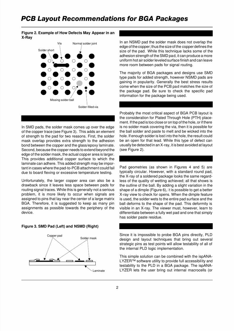
Figure 2. Example of How Defects May Appear in an
X-Ray
Normal solder jointVia
Missing solder ball
Solder-filled via
Solder short
Non-Solder Mask Defined Pads
In an NSMD pad the solder mask does not overlap theedge of the copper; thus the size of the copper defines thesize of the pad. While this technique lacks some of the
adhesion strength of the SMD pad, it can produce a moreuniform hot air solder leveled surface finish and can leave
more room between pads for signal routing.
The majority of BGA packages and designs use SMDtype pads for added strength, however NSMD pads aregaining in popularity. Generally the best stress results
come when the size of the PCB pad matches the size ofthe package pad. Be sure to check the specific pad
information for the package being used.
Plated Through Hole Placement
Probably the most critical aspect of BGA PCB layout is
the consideration for Plated Through Hole (PTH) place-ment. If the pad is too close or on top of the hole, or if thereis no solder mask covering the via, then it is possible for
the ball solder and paste to melt and be wicked into thehole. If enough solder is lost into the hole, the result could
be an open for that lead. While this type of defect canusually be detected in an X-ray, it is best avoided at layout
(see Figure 2).
Pad Geometries
Pad geometries (as shown in Figures 4 and 5) aretypically circular. However, with a standard round pad,
the X-ray of a soldered package looks the same regard-less of the quality of wetting achieved; all that shows is
the outline of the ball. By adding a slight variation in theshape of a dimple (Figure 6), it is possible to get a better
X-ray view to check for opens. When the dimple featureis used, the solder wets to the entire pad surface and the
ball deforms to the shape of the pad. This deformity isvisible in an X-ray. The viewer must, however, learn todifferentiate between a fully wet pad and one that simply
has solder paste residue.
Layout Recommendations for Testability
Since it is impossible to probe BGA pins directly, PLD
design and layout techniques that bring out severalstrategic pins as test points will allow testability of all of
the internal PLD logic implementation.
This simple solution can be combined with the ispANA-
LYZER™ software utility to provide full accessibil ity andtestability to the PLD in a BGA package. The ispANA-
LYZER lets the user bring out internal macrocells (or
Figure 3. SMD Pad (Left) and NSMD (Right)
Laminate
Copper padSolder mask
8/3/2019 PCB Layout Recommendation for BGA
http://slidepdf.com/reader/full/pcb-layout-recommendation-for-bga 3/3
PCB Layout Recommendations for BGA Packages
3
other macrocell outputs) to unused I/O pins. With thiscapability, a suspect I/O pin can be tested via a test point
that is designed to bring out a number of predefined I/Opins.
Another option is to make use of a Lattice ispGDX™ or
ispGDS™ switch matrix device. These devices are de-signed to route signals, allowing the pinout of the BGA tochange without affecting the layout of the board. By
routing some or all of the BGA traces through a GDX you
add complete flexibility to the pinout of the BGA device.The use of an ispGDX or ispGDS device can be espe-cially powerful when used in conjunction with the
ispANALYZER utility.
For additional information on the Lattice ispGDX and
ispGDS devices or the ispANALYZER software utility,contact your local Lattice sales office or Field ApplicationEngineer, or visit the Lattice Semiconductor website at
http:\\www.latticesemi.com.
Conclusion
Armed with a few simple layout tips, most of the difficul-
ties in switching from QFP to BGA package use can be
overcome. BGA packages are tolerant to misalignmentand with the help of an X-ray machine it is easy to spotmanufacturing defects and guarantee high PCB quality.
Figure 5. SMD Pad with Example Dimensions
Solder maskover copper
Solderablesurface
4 mil solder maskoverlap
23 mil solder maskopening diameter
31 mil solder paddiameter
Figure 4. NMSD Dogbone with Typical Dimenstions
for Most 1.27mm Pitch PBGAs
Barelaminate
Solder maskover copper
Solderablesurface
4 mil solder maskto pad clearance
35.4 mils
25 mil via diameter
14 mil drilled via diameter(12 mil finished diameter)
8 mil trace width
23 mil solderpad diameter
31 mil solder maskopening diameter
Figure 6. Examples of Solder Pad Bumps (Also Called
Dimples or Ears)


![de partido a su piscina… - BINDER · Tipo BGA 160 BGA 215 BGA 275 BGA 320 BGA 430 BGA 550 BGA 600 BGA 1200 Tensión de conexión [VAC] 230 230 230 230 230 230 230 230 Rango de frecuencia](https://img.pdfslide.net/doc/110x75/5c132e8509d3f26c7c8c5e0d/de-partido-a-su-piscina-binder-tipo-bga-160-bga-215-bga-275-bga-320-bga-430.jpg)