Embed Size (px)
Citation preview

PCBs in Building Materials:
A Consultant Perspective
Robert L. May Jr.
January 6, 2011

2
Outline ● Background
● Reactions
● Building Materials
● Remediation Process
● Consultant Challenges
● Cost Analysis
● Case Study
Background

4
What Are PCBs? ● Polychlorinated biphenyls
● A group of man-made chemicals
209 congeners which is any single, unique
chemical compound in the PCB category
Different degradability
Potential Toxicity varies
9 Homologs which are subcategories of
PCB congeners having equal numbers of chlorine
PCBs are very stable
No known natural sources of PCBs
Nearly everybody has traces in body Commonly known to be used in electrical equipment, industrial processes, and
manufacturing
Common Trade Name: Aroclor (16 types)
Banned from production in 1979
● Non-polar/hydrophobic
Do not easily dissolve in water
Binds strongly to sediment particles
Fat soluble and stored in an organism's fatty tissue
dep.state.ct.us/wst/pcb/pcbindex.htm www.epa.gov/pcb/ www.trwnews.net/isdioxindangerous.htm
1
3’
2’1’
54
3
2
4’5’
1
3’
2’1’
54
3
2
4’5’
1
3’
2’1’
54
3
2
4’5’
Structure of Polychlorinated Biphenyl

5
Brief History ● 1881: First Synthesis
● 1914: Measurable amount in bird feathers
● 1927: PCBs first manufactured in Alabama (Swann)
● 1929 PCBs were domestically manufactured
● 1930’s: First worker health problems & studies
● 1935: Monsanto bought Swann
● 1947: GE began using PCBs in electrical equipment
● 1950’s: Toxicity of PCBs of concern but not fully acted on
● 1960’s: Increasing awareness of PCB hazards
● 1968: 1300 Japanese residents ate rice contaminated with PCBs
● 1970’s: Increased study into PCBs toxicity
● 1970’s: Government gets involved
● 1979: EPA issues final regulations banning manufacture of PCBs
● Late 1980’s: Companies cleanup and stop using PCBs
● Early 90’s: EPA declares PCB carcinogens, endocrine disruptors, and reproductive toxins
● 2000: United Nations Environment Program committee ban on PCBs
● 2009: Guidance for Caulking related to schools
● 2010: Advanced Notice of pending Rule Changes (6 Public Meetings Held)
Adapted from: “Lake Michigan Mass Balance Study - PCB Modeling Report” Ronald Rossmann, Editor, EPA-600/R-04/167 December 2006

Reactions
7
Harvard Study ● July 2004 – HSPH Press Release
● 24 Buildings Tested
● 1/3 or 8 of 24 Exceeded 50 ppm PCB
● Up to 33,000 ppm PCB
● Caulk Unrecognized and Widespread Source of PCBs
● Recommends Routine Testing of Caulk
Robert F. Herrick, Michael D. McClean, John D. Meeker, Lisa K.
Baxter, George A. Weymouth. “An Unrecognized Source of PCB
Contamination in Schools and Other Buildings.” Environmental
Health Perspectives. 2004, 112 (10), 1051.

8
Boston Globe – Sept. 2009
9
Regulations
● PCBs in caulking and sealant materials was never authorized by EPA for use
Use is not authorized
Highly unlikely to be authorized
● EPA 40 CFR part 761 (
761)
Marking
Manufacture
Processing
Distribution
Use
Storage
Disposal

10
Federal Response to PCBs
● EPA Region 2 response Nov 3, 2005
No visual differences between PCB and non-PCB caulk
Testing “may be advisable”
“use of PCBs in caulking...has never been authorized... because it is illegal and the potential for exposure is significant, PCB containing caulk must be removed upon discovery.”
Remediation and disposal covered under current regulations (40 CFR part 761)
● EPA Released guidance documents
in 2009
11
Federal Response to PCBs So What is EPA telling the Public?
● Focus has been toward guidance for Schools Many Fact Sheets and Guidance Documents Available from EPA
● Guidance suggests testing air in school buildings Public Health Levels for PCB established by EPA.
● EPA suggests that removal of PCB caulking should occur during renovations or repairs for buildings built or renovated between 1950 and 1978. In order to know if PCBs present will require testing
● Test caulking if damaged, such as peeling brittle, cracking or visibly deteriorating and properly remove if PCBs present at “significant levels” A significant level would be at regulated concentration of 50 ppm or
greater
● EPA is planning to study PCBs over next two years to develop further recommendations

12
Media Coverage ● URI Chafee Social Science Center Building in Kingston
Campus, URI News Bureau 2000
● Harvard Study, Boston Globe 2004
● UMASS Amherst Science Building, Daily New Hampshire Gazette 2006
● New Bedford H.S. Standard Times 2006
● Doherty Memorial H.S., Worcester Telegram & Gazette Corp 2009
● Berkshire Community College, Berkshire Eagle 2009
● Crompton Park Pool Worcester Telegram & Gazette Corp 2010
● Lexington Estabrook School, Boston Globe 2010
● CT Technical Schools Tested 2010, New Haven Register
● New York, EPA Pilot Study, Three Schools Elevated PCB air levels, West Side Spirit 2010
*source: www.pcbinschools.org

PCBs in Building Materials

14
Properties of PCBs
Low Flammability
Chemically Stable
Fire Resistant
Electrical Insulator
Softener and Plasticizer
Durable and resistant to
degradation

15
PCB Uses
U.S. Industry Use of
PCBs (1929-1975)
1.2 Million Pounds
Capacitors and
Transformers (>75% of
total usage)
Plasticizer (<10% of total
usage)
Miscellaneous Industrial
Applications >2% of total
usage
Sourec EPA, January 30, 1997.

16
PCB Uses Commercial Use of PCBs
Although no longer commercially produced in the United States, PCBs may be present
in products and materials produced before the 1979 PCB ban. Products that may
contain PCBs include:
● Transformers and capacitors
● Other electrical equipment including voltage regulators, switches, re-closers, bushings, and electromagnets
● Oil used in motors and hydraulic systems
● Old electrical devices or appliances containing PCB capacitors
● Fluorescent light ballasts
● Cable insulation
● Thermal insulation material including fiberglass, felt, foam, and cork
● Adhesives and tapes
● Oil-based paint
● Caulking
● Plastics
● Carbonless copy paper
● Floor finish

17
Suspect Building Materials
Remediation Process

19
Remediation Decision Tree
Source-www.epa.gov

20
Remediation Steps 1. Identify suspect PCB material
Physical inspection
Identify pre-1980 construction
Review of architecture plans
Review construction and remodeling history
2. Sample and Test Suspect materials
Adjacent material
Air
Soil
3. Determine exposure level How often people interact with material?
How could people interact with material?
4. Determine method to minimize exposure Removal
Barrier
5. Disposal Verify PCB material left is below allowable concentration
Unregulated waste
Regulated waste

21
1. Identify Suspect material
22
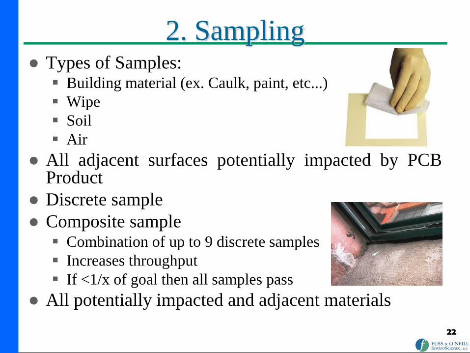
2. Sampling ● Types of Samples:
Building material (ex. Caulk, paint, etc...)
Wipe
Soil
Air
● All adjacent surfaces potentially impacted by PCB Product
● Discrete sample
● Composite sample Combination of up to 9 discrete samples
Increases throughput
If <1/x of goal then all samples pass
● All potentially impacted and adjacent materials
23
2. Sampling
● Bulk Source Materials Containing ≥50 ppm
PCBs are regulated.
● Materials containing less than 50 ppm PCBs,
must determine if an “Excluded PCB Product”
as defined in
761.3 below.
The products or source of the products containing
< 50 ppm concentration PCBs were legally
manufactured, processed, distributed in commerce,
or used before October 1, 1984.

24
2. Testing ● Extraction
EPA Method 3500B/3540C
Soxhlet
● Analyze the extracted material
EPA Method 8082
● Air Sampling
EPA Method TO-4A or TO-10A
Aroclor – All or Specific
Homologs - 9
Congener – 209
EPA may specify detection limits
<0.1 micrograms/cubic meter
<0.05 micrograms/cubic meter
whale.wheelock.edu/bwcontaminants/analysis.
html

25
3. Exposure Determination
● Frequency
How often there is potential contact?
● Duration
How long is the contact?
● Occupancy
High
Low
26
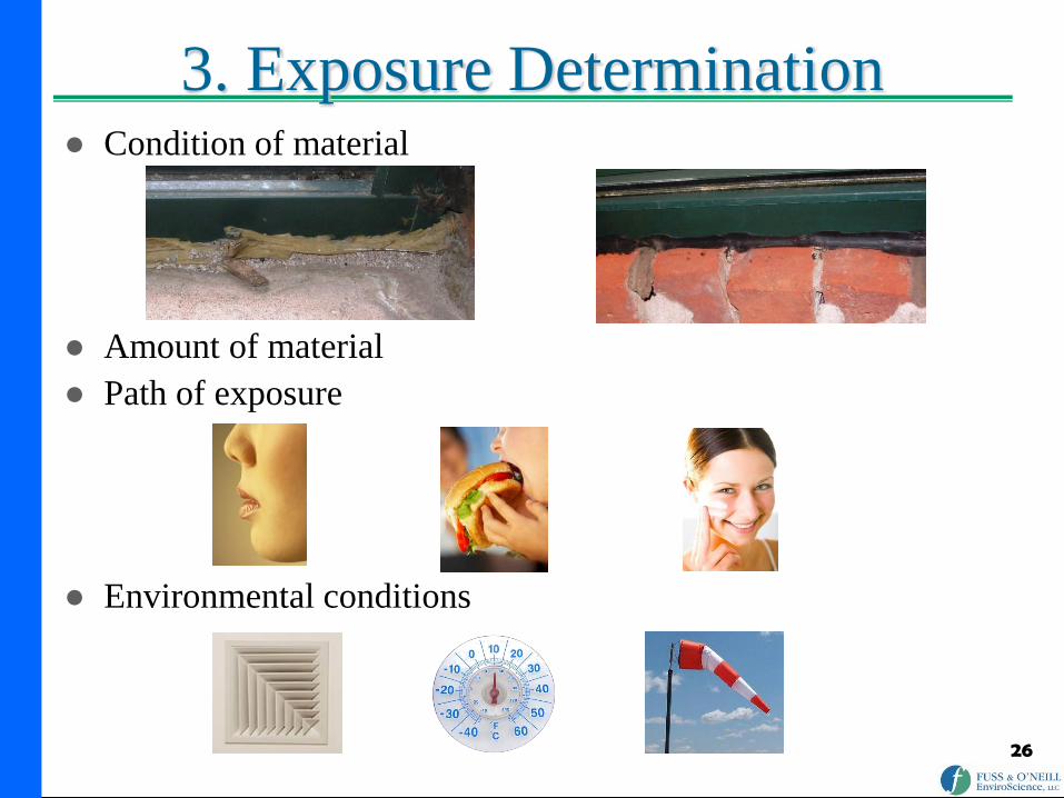
3. Exposure Determination ● Condition of material
● Amount of material
● Path of exposure
● Environmental conditions

27
4. Removal Considerations ● EPA has three methods:
A. Performance-based
B. Self-implementing
C. Risk-based
● PCB bulk product waste “material” Solids
≥50 ppm PCBs at time of designation as waste
● PCB remediation waste “material” Waste as result of spill, release, or unauthorized disposal
No concentration set in definition
● Method depends on: Exposure evaluation and project intent
Concentration of PCBs in material
Time for completion
28
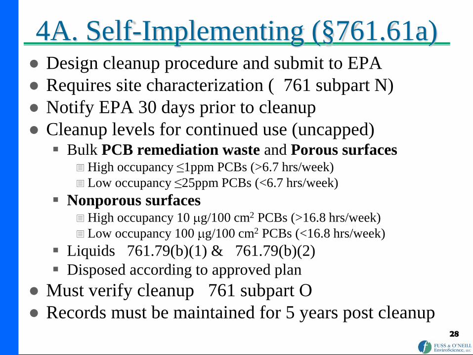
4A. Self-Implementing (§761.61a) ● Design cleanup procedure and submit to EPA
● Requires site characterization (
761 subpart N)
● Notify EPA 30 days prior to cleanup
● Cleanup levels for continued use (uncapped) Bulk PCB remediation waste and Porous surfaces
High occupancy ≤1ppm PCBs (>6.7 hrs/week)
Low occupancy ≤25ppm PCBs (<6.7 hrs/week)
Nonporous surfaces High occupancy 10 g/100 cm2 PCBs (>16.8 hrs/week)
Low occupancy 100 g/100 cm2 PCBs (<16.8 hrs/week)
Liquids
761.79(b)(1) &
761.79(b)(2)
Disposed according to approved plan
● Must verify cleanup
761 subpart O
● Records must be maintained for 5 years post cleanup
29
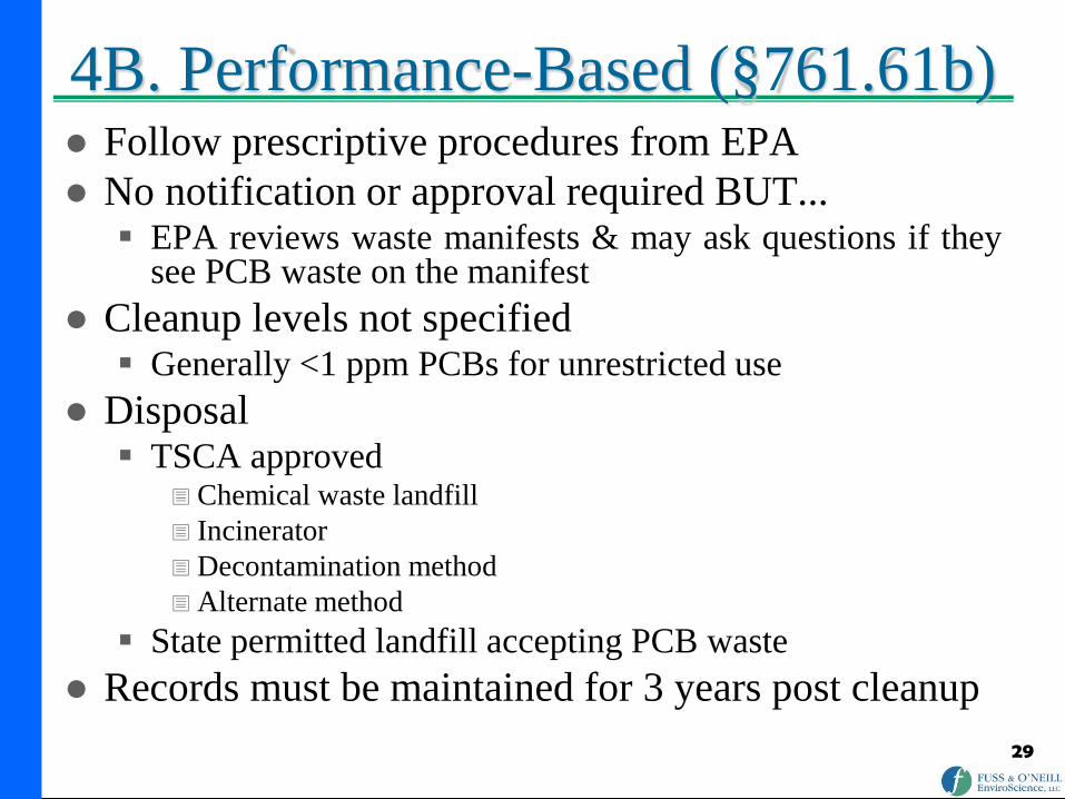
4B. Performance-Based (§761.61b) ● Follow prescriptive procedures from EPA
● No notification or approval required BUT... EPA reviews waste manifests & may ask questions if they
see PCB waste on the manifest
● Cleanup levels not specified Generally <1 ppm PCBs for unrestricted use
● Disposal TSCA approved
Chemical waste landfill
Incinerator
Decontamination method
Alternate method
State permitted landfill accepting PCB waste
● Records must be maintained for 3 years post cleanup
30
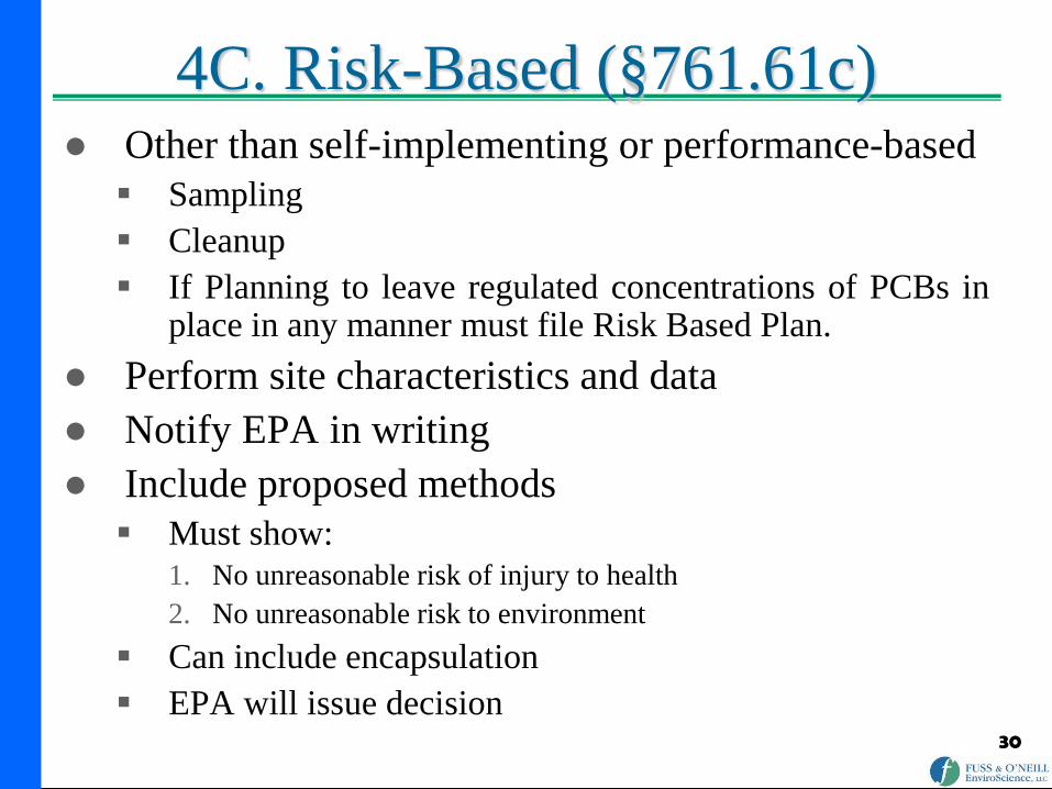
4C. Risk-Based (§761.61c) ● Other than self-implementing or performance-based
Sampling
Cleanup
If Planning to leave regulated concentrations of PCBs in place in any manner must file Risk Based Plan.
● Perform site characteristics and data
● Notify EPA in writing
● Include proposed methods
Must show:
1. No unreasonable risk of injury to health
2. No unreasonable risk to environment
Can include encapsulation
EPA will issue decision

31
5. Disposal
● Verification
Sampling
Analysis
Reports
● All data must be organized so that EPA can
review
● Reports kept on file

32
5. Disposal ● Any material ≥50 ppm PCBs
PCB bulk product waste (
761 subpart 62)
Disposal options TSCA approved
– Chemical waste landfill
– Incinerator
– Decontamination method
– Alternate method
State permitted landfill accepting PCB waste
Does not require EPA approval - generally
● Adjacent material <50 ppm PCBs PCB remediation waste (
761 subpart 61)
Disposal options {above options}
EPA approved method based on work plan – Must obtain EPA approval
33
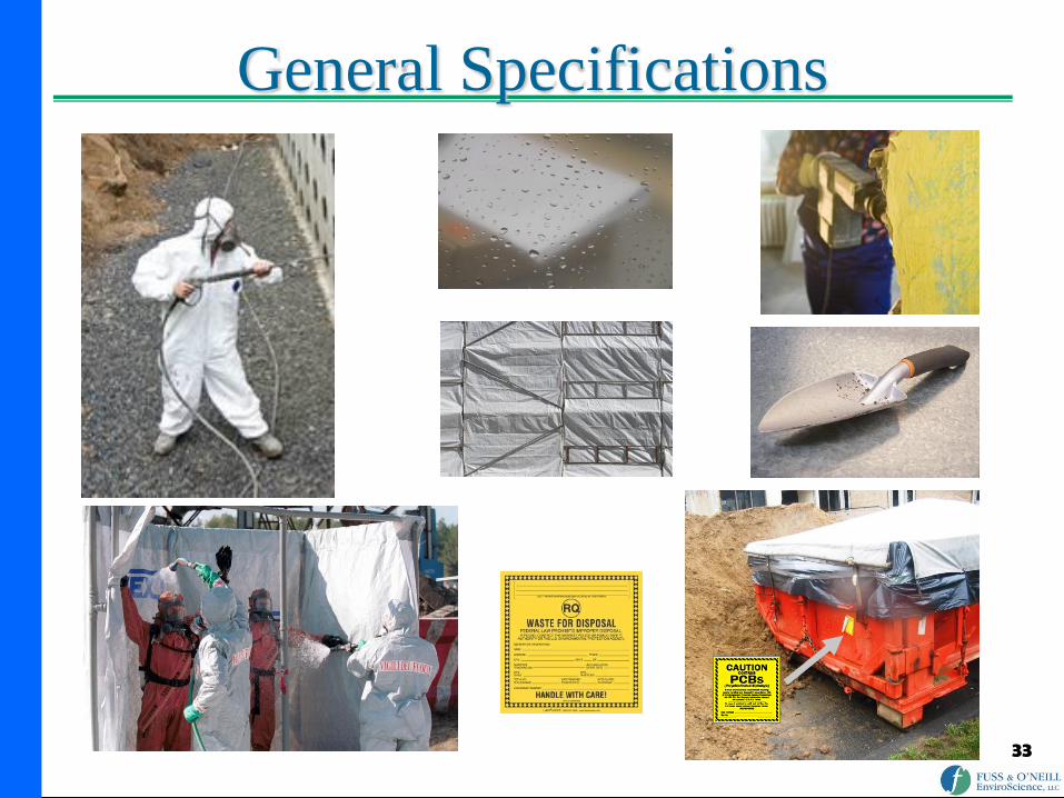
General Specifications
Consultant Challenges

35
Consultant Challenges
● EPA does not mandate by regulation testing of
material.
● Each site is treated by EPA as a unique site
with potentially different requirements for
containment, post cleaning standards, post
verification and introduction of wipe and air
sampling for clearance.
● Client’s can be reluctant to test since not
mandated by EPA prior to renovation or
demolition unlike asbestos.
36
Consultant Challenges
● Project planning for renovation EPA has
indicated in guidance should be tested.
● Testing early enough in the process to be able
to plan and budget for work ends up requiring
potential interim sampling of air and wipe and
possible interim measures until such time as
materials are removed.
● If it is determined that PCB found inside
building in air or wipes, reactions of school
could be publically criticized.

37
Consultant Challenges
● Consultant must be knowledgeable of the process and familiar with current EPA positions.
● Consultant should suggest pro-active steps to assist schools and other clients in the process.
● For schools this should include full disclosure of intent to sample with public transparency with regard to results and findings.
● Sequence testing work such that decisions and knowledge of risk can be determined early in the process.
38
Consultant Challenges ● Prepare the clients for the time frames and cost
associated with all the testing steps. Source Materials
Adjacent Materials
Air and Wipe
● Prepare the clients for the time frames and allowances for EPA review and need for likely changes of Plans under 761.61(a).
● Discuss cost implications with client of the entire process and remediation. The costs for PCB Remediation and required post verification are more costly than similar building material contaminants such as asbestos.

39
Consultant Challenges
● PCBs in building materials is newer area of concern
being addressed in the market. As such contractors,
and consultants may not all be on same page
depending on their experience.
● Take part and stay on top of what is happening in the
industry.
● Look into local requirements and sensitivity to the
topic where work is being performed.
● Some states have different requirements and many
local communities are more sensitive from media
coverage.

Cost Analysis
41
PCB Cost Implications
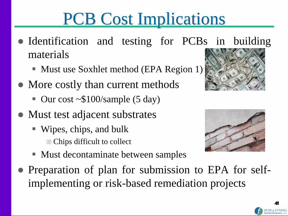
● Identification and testing for PCBs in building
materials
Must use Soxhlet method (EPA Region 1)
● More costly than current methods
Our cost ~$100/sample (5 day)
● Must test adjacent substrates
Wipes, chips, and bulk
Chips difficult to collect
Must decontaminate between samples
● Preparation of plan for submission to EPA for self-
implementing or risk-based remediation projects
42
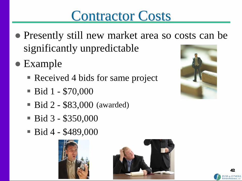
Contractor Costs
● Presently still new market area so costs can be
significantly unpredictable
● Example
Received 4 bids for same project
Bid 1 - $70,000
Bid 2 - $83,000
Bid 3 - $350,000
Bid 4 - $489,000
(awarded)
43
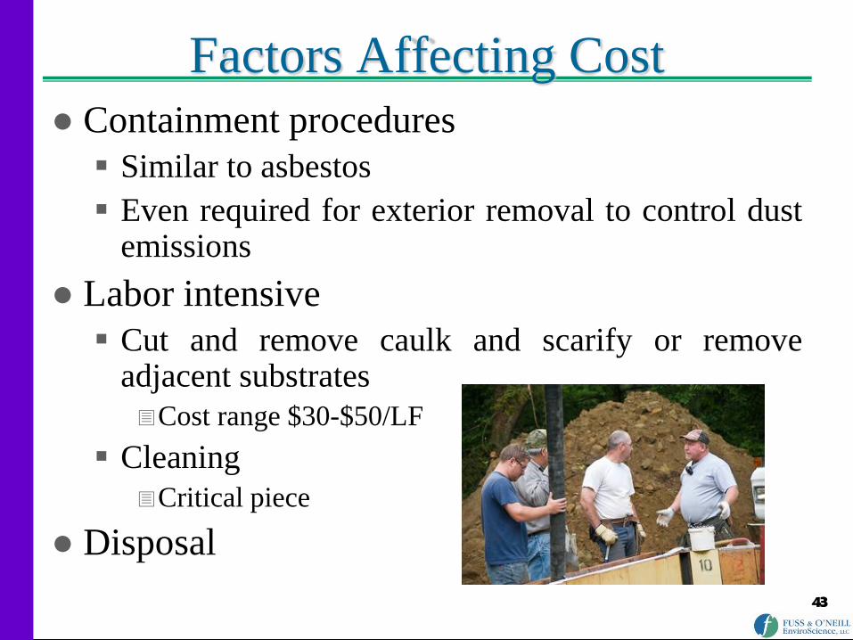
Factors Affecting Cost
● Containment procedures
Similar to asbestos
Even required for exterior removal to control dust emissions
● Labor intensive
Cut and remove caulk and scarify or remove adjacent substrates
Cost range $30-$50/LF
Cleaning
Critical piece
● Disposal
44
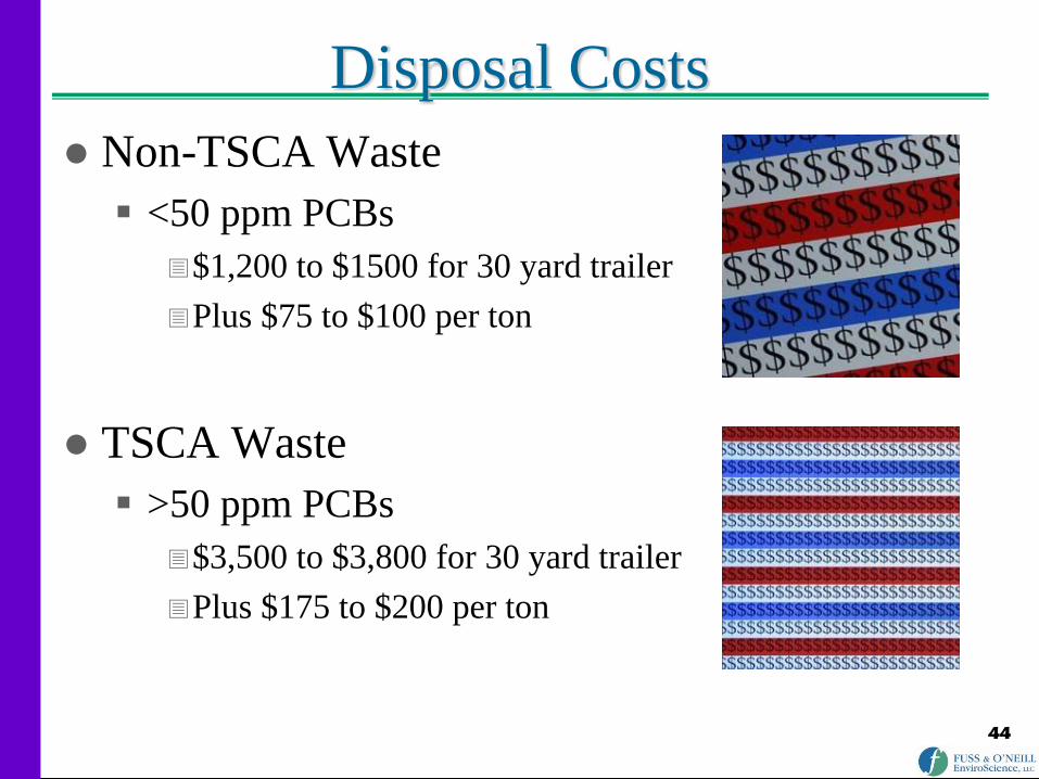
Disposal Costs
● Non-TSCA Waste
<50 ppm PCBs
$1,200 to $1500 for 30 yard trailer
Plus $75 to $100 per ton
● TSCA Waste
>50 ppm PCBs
$3,500 to $3,800 for 30 yard trailer
Plus $175 to $200 per ton

Case Study

46
Case Study – Overview ● Project to demolish existing school buildings
Darling Library
Baxter Building
● A consultant tested for PCBs after project bid but prior to full demolition
● Mixed PCBs results
Extreme highs and lows
Tests showed almost all caulking on both buildings >50 ppm PCBs
West Elevation: Baxter Building. North Elevation: Darling Library (left) and Baxter
Building (right) showing connector.

47
Case Study – First Step ● Fuss & O’Neill requested to assist with removal of caulking to
facilitate demolition
● Buildings needed to be demolished before start of school
About 2 months
● Prior Consultant sampling needed further characterization
Possible cross contamination of samples
● Caulk in both buildings was resampled
Proper decontamination was performed
Also sampled adjacent porous surfaces to determine PCB concentration
● Results
Many areas contained no PCB caulking
Darling Library had no PCB caulking
Allowed demolition
48
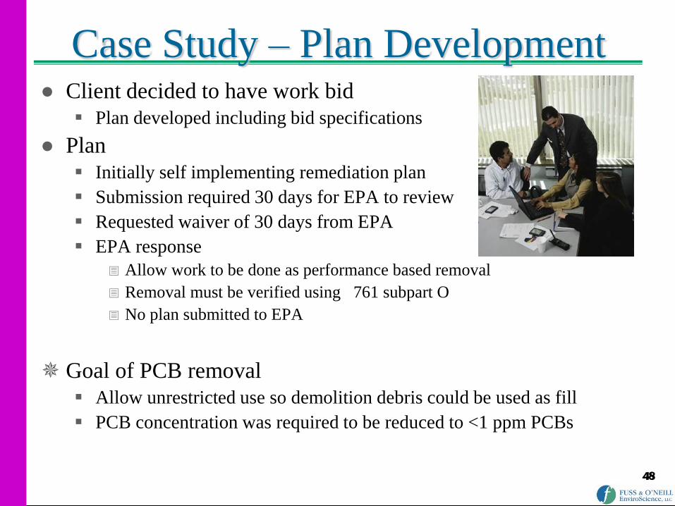
Case Study – Plan Development ● Client decided to have work bid
Plan developed including bid specifications
● Plan
Initially self implementing remediation plan
Submission required 30 days for EPA to review
Requested waiver of 30 days from EPA
EPA response
Allow work to be done as performance based removal
Removal must be verified using
761 subpart O
No plan submitted to EPA
Goal of PCB removal
Allow unrestricted use so demolition debris could be used as fill
PCB concentration was required to be reduced to <1 ppm PCBs

49
Case Study – Removal ● Bids received
Company selected to perform work
● Work on exterior was performed on enclosed lifts Control dust emissions
● Materials adjacent to caulk cut or removed Brick, concrete, and limestone
Whole sections for some structures
Disposed of as TSCA waste >50 ppm PCBs
● Samples Verification samples collected every 5 linear feet (
761 subpart O)
Four samples were composited to decrease analysis cost
Several locations failed initial verification sampling Additional removal of adjacent substrates was performed
● Contractor tried using cleaning product Capsur® to wash surfaces where cutting had occurred Used due to extreme depths into substrate not observed in initial
sampling
Resulted in passing verification samples
Did not require further cutting into substrates in most locations
● Next slide shows some of the locations after removal

50
Case Study – Pictures

51
Case Study – Results ● Soil adjacent to buildings also had elevated PCB content and
was removed.
● All waste disposed as TSCA regulated waste containing >50 ppm PCBs as required under a performance based removal project.
● Demolition schedule was essentially maintained and buildings were demolished.

52
Contact
● Fuss & O’Neill, EnviroScience, LLC
50 Redfield Street
Boston, MA 02122
(617) 282-4675
317 Iron Horse Way
Providence, RI 02908
(401) 861-3070