Embed Size (px)
Citation preview
NJW4153
- 1 -Ver.2013-03-21
Switching Regulator IC for Buck Converter Current Mode Control w/ 40V/1A MOSFET
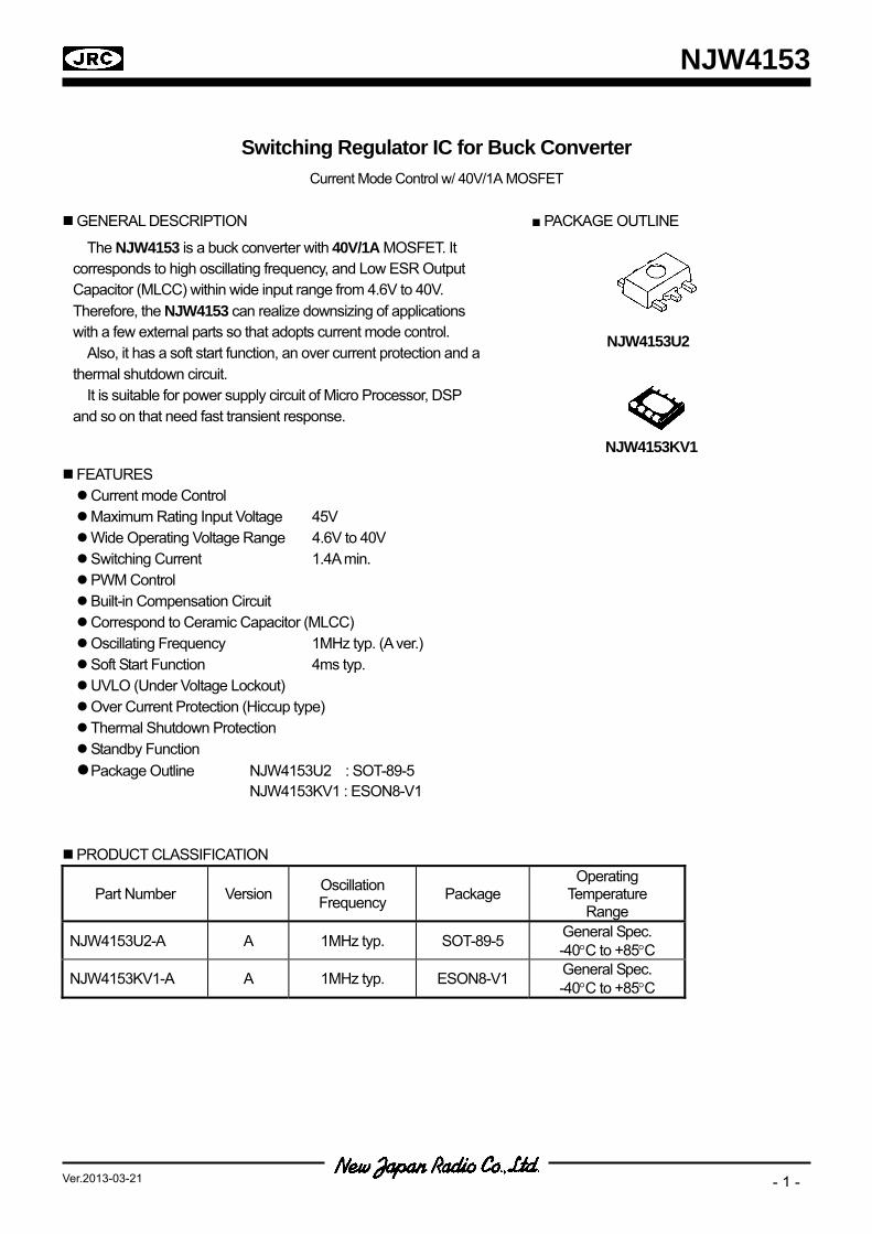
GENERAL DESCRIPTION PACKAGE OUTLINE
FEATURES Current mode Control Maximum Rating Input Voltage 45V Wide Operating Voltage Range 4.6V to 40V Switching Current 1.4A min. PWM Control Built-in Compensation Circuit Correspond to Ceramic Capacitor (MLCC) Oscillating Frequency 1MHz typ. (A ver.) Soft Start Function 4ms typ. UVLO (Under Voltage Lockout) Over Current Protection (Hiccup type) Thermal Shutdown Protection Standby Function Package Outline NJW4153U2 : SOT-89-5
NJW4153KV1 : ESON8-V1 PRODUCT CLASSIFICATION
Part Number Version Oscillation Frequency Package
Operating Temperature
Range
NJW4153U2-A A 1MHz typ. SOT-89-5 General Spec. -40°C to +85°C
NJW4153KV1-A A 1MHz typ. ESON8-V1 General Spec. -40°C to +85°C
The NJW4153 is a buck converter with 40V/1A MOSFET. It corresponds to high oscillating frequency, and Low ESR Output Capacitor (MLCC) within wide input range from 4.6V to 40V. Therefore, the NJW4153 can realize downsizing of applications with a few external parts so that adopts current mode control.
Also, it has a soft start function, an over current protection and a thermal shutdown circuit.
It is suitable for power supply circuit of Micro Processor, DSP and so on that need fast transient response.
NJW4153U2
NJW4153KV1
NJW4153
- 2 - Ver.2013-03-21
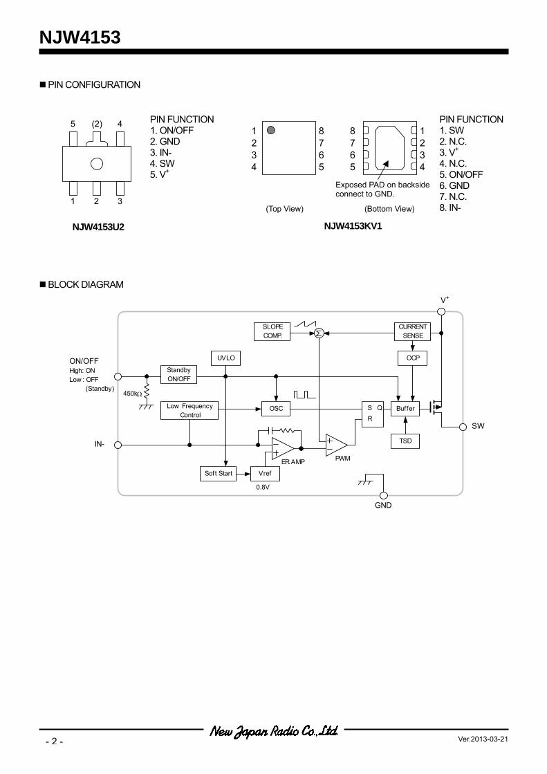
PIN CONFIGURATION
BLOCK DIAGRAM
V+
IN-
ER⋅AMP
Buffer
OCP
CURRENTSENSE
TSD
VrefSoft Start
UVLO
SLOPECOMP.
0.8V
S QR
OSC
GND
High: ONLow : OFF (Standby)
ON/OFF
SW
PWM
StandbyON/OFF
Low FrequencyControl
450kΩ
PIN FUNCTION 1. ON/OFF 2. GND 3. IN- 4. SW 5. V+
NJW4153U2
1 2 3
4 5 (2)
NJW4153KV1
1 2 3 4
Exposed PAD on backside connect to GND.
8765
1234
8765
(Top View) (Bottom View)
PIN FUNCTION 1. SW 2. N.C. 3. V+ 4. N.C. 5. ON/OFF 6. GND 7. N.C. 8. IN-
NJW4153
- 3 -Ver.2013-03-21
ABSOLUTE MAXIMUM RATINGS (Ta=25°C)
PARAMETER SYMBOL MAXIMUM RATINGS UNIT Supply Voltage V+ +45 V V+- SW pin Voltage VV-SW +45 V IN- pin Voltage VIN- -0.3 to +6 V ON/OFF pin Voltage VON/OFF +45 V
Power Dissipation PD
SOT-89-5 ESON8-V1
625 (*1) 2,400 (*2)
600 (*3) 1,800 (*4)
mW
Junction Temperature Range Tj -40 to +150 °C Operating Temperature Range Topr -40 to +85 °C Storage Temperature Range Tstg -40 to +150 °C
(*1): Mounted on glass epoxy board. (76.2×114.3×1.6mm:based on EIA/JDEC standard size, 2Layers, Cu area 100mm2) (*2): Mounted on glass epoxy board. (76.2×114.3×1.6mm:based on EIA/JDEC standard, 4Layers)
(For 4Layers: Applying 74.2×74.2mm inner Cu area and a thermal via hall to a board based on JEDEC standard JESD51-5) (*3): Mounted on glass epoxy board. (101.5×114.5×1.6mm: based on EIA/JEDEC standard, 2Layers FR-4, with Exposed Pad) (*4): Mounted on glass epoxy board. (101.5×114.5×1.6mm: based on EIA/JEDEC standard, 4Layers FR-4, with Exposed Pad)
(For 4Layers: Applying 99.5×99.5mm inner Cu area and a thermal via hole to a board based on JEDEC standard JESD51-5) RECOMMENDED OPERATING CONDITIONS
PARAMETER SYMBOL MIN. TYP. MAX. UNIT Supply Voltage V+ 4.6 – 40 V
NJW4153
- 4 - Ver.2013-03-21
ELECTRICAL CHARACTERISTICS (Unless otherwise noted, V+=VON/OFF=12V, Ta=25°C)
PARAMETER SYMBOL TEST CONDITION MIN. TYP. MAX. UNIT Under Voltage Lockout Block
ON Threshold Voltage VT_ON V+= L → H 4.3 4.45 4.6 V OFF Threshold Voltage VT_OFF V+= H → L 4.2 4.35 4.5 V Hysteresis Voltage VHYS 70 100 – mV Soft Start Block
Soft Start Time TSS VB=0.75V 2 4 8 ms Oscillator Block
Oscillation Frequency fOSC A version, VIN-=0.7V 900 1,000 1,100 kHz Oscillation Frequency (Low Frequency Control) fOSC_LOW VIN-=0.4V – 370 – kHz
Oscillation Frequency deviation (Supply voltage) fDV V+=4.6 to 40V – 1 – %
Oscillation Frequency deviation (Temperature) fDT Ta= -40°C to +85°C – 5 – %
Error Amplifier Block
Reference Voltage VB -1.0% 0.8 +1.0% V Input Bias Current IB -0.1 – +0.1 µA PWM Comparate Block
Maximum Duty Cycle MAXDUTY VIN-=0.7V 85 90 – % Minimum ON time tON-min – 140 180 ns Over Current Protection Block
Cool Down Time tCOOL – 8 – ms Output Block
Output ON Resistance RON ISW=1A – 0.45 0.75 Ω Switching Current Limit ILIM 1.4 1.9 2.4 A SW Leak Current ILEAK VON/OFF=0V, V+=45V, VSW=0V – – 1 µA ON/OFF Block
ON Control Voltage VON VON/OFF= L → H 1.6 – V+ V OFF Control Voltage VOFF VON/OFF= H → L 0 – 0.5 V Pull-down Resistance RPD – 450 – kΩ General Characteristics
Quiescent Current IDD RL=no load, VIN-=0.7V – 3.9 4.4 mA Standby Current IDD_STB VON/OFF=0V – – 1 µA
NJW4153
- 5 -Ver.2013-03-21
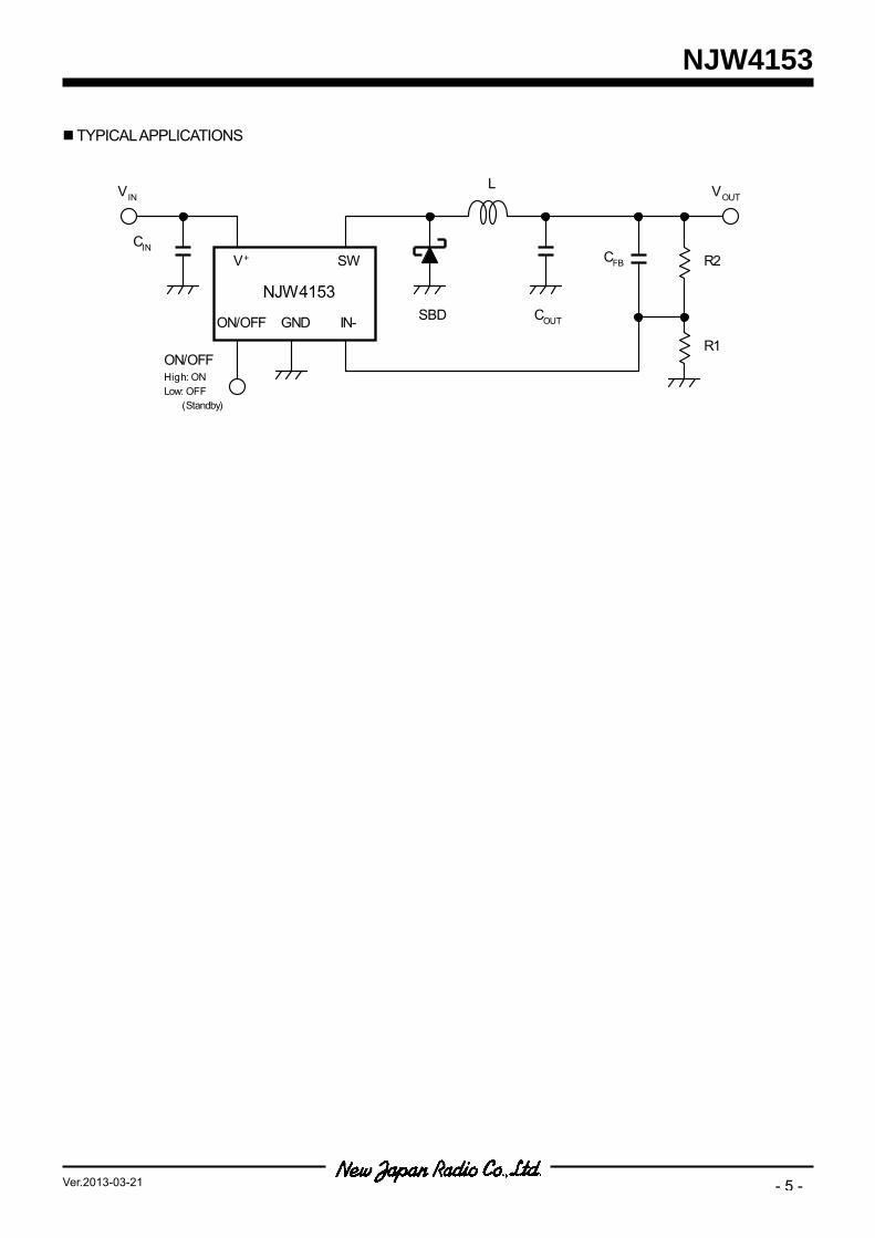
TYPICAL APPLICATIONS
SW
GND IN-
V+
NJW4153
ON/OFF
CFB R2
COUT
L
SBD
VIN
CIN
R1
VOUT
ON/OFFHigh: ONLow: OFF (Standby)

NJW4153
- 6 - Ver.2013-03-21
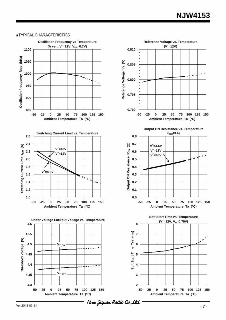
TYPICAL CHARACTERISTICS
Reference Voltage vs. Supply Voltage(Ta=25°C)
0.79
0.795
0.8
0.805
0.81
0 10 20 30 40Supply Voltage V+ (V)
Ref
eren
ce V
olta
ge V
B (
V)Quiescent Current vs. Supply Voltage
(RL=no load, VIN-=0.7V, Ta=25°C)
0
1
2
3
4
5
0 10 20 30 40Supply Voltage V+ (V)
Qui
esce
nt C
urre
nt I
DD (
mA
)
Oscillation Frequency vs. Supply Voltage(A ver., VIN-=0.7V, Ta=25°C)
980
990
1000
1010
1020
0 10 20 30 40Supply Voltage V+ (V)
Osc
illat
ion
Freq
unec
ny f
OSC
(kH
z)
NJW4153
- 7 -Ver.2013-03-21
TYPICAL CHARACTERISTICS
Reference Voltage vs. Temperature(V+=12V)
0.790
0.795
0.800
0.805
0.810
-50 -25 0 25 50 75 100 125 150Ambient Temperature Ta (°C)
Ref
eren
ce V
olta
ge V
B (
V)
Switching Current Limit vs. Temperature
1.0
1.2
1.4
1.6
1.8
2.0
2.2
2.4
2.6
-50 -25 0 25 50 75 100 125 150Ambient Temperature Ta (°C)
Switc
hing
Cur
rent
Lim
it I L
IM (
A)
V+=4.6V
V+=40VV+=12V
Output ON Resistance vs. Temperature(ISW=1A)
0.0
0.1
0.2
0.3
0.4
0.5
0.6
0.7
0.8
-50 -25 0 25 50 75 100 125 150Ambient Temperature Ta (°C)
Out
put O
N R
esis
tanc
e R
ON (Ω
)
V+=4.6VV+=12VV+=40V
Under Voltage Lockout Voltage vs. Temperature
4.3
4.35
4.4
4.45
4.5
4.55
4.6
-50 -25 0 25 50 75 100 125 150Ambient Temperature Ta (°C)
Thre
shol
d Vo
ltage
(V)
VT_ON
VT_OFF
Soft Start Time vs. Temperature(V+=12V, VB=0.75V)
2
3
4
5
6
7
8
-50 -25 0 25 50 75 100 125 150Ambient Temperature Ta (°C)
Soft
Star
t Tim
e T
ss (
ms)
Oscillation Frequency vs Temperature(A ver., V+=12V, VIN-=0.7V)
850
900
950
1000
1050
1100
-50 -25 0 25 50 75 100 125 150Ambient Temperature Ta (°C)
Osc
illat
ion
Freq
uenc
y fo
sc (
kHz)
NJW4153
- 8 - Ver.2013-03-21
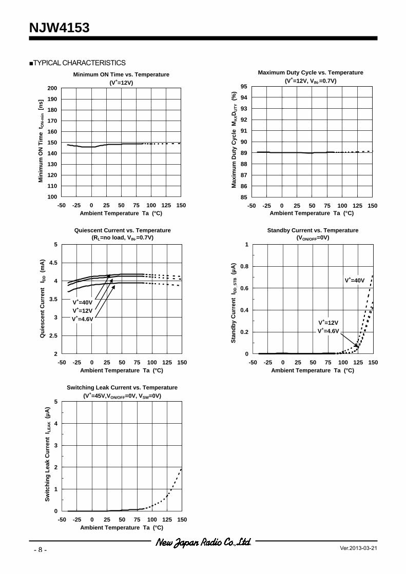
TYPICAL CHARACTERISTICS
Quiescent Current vs. Temperature(RL=no load, VIN-=0.7V)
2
2.5
3
3.5
4
4.5
5
-50 -25 0 25 50 75 100 125 150Ambient Temperature Ta (°C)
Qui
esce
nt C
urre
nt
I DD (
mA
)
V+=40VV+=12VV+=4.6V
Standby Current vs. Temperature(VON/OFF=0V)
0
0.2
0.4
0.6
0.8
1
-50 -25 0 25 50 75 100 125 150Ambient Temperature Ta (°C)
Stan
dby
Cur
rent
ID
D_S
TB (
µA)
V+=40V
V+=12VV+=4.6V
Switching Leak Current vs. Temperature(V+=45V,VON/OFF=0V, VSW=0V)
0
1
2
3
4
5
-50 -25 0 25 50 75 100 125 150Ambient Temperature Ta (°C)
Switc
hing
Lea
k C
urre
nt I
LEA
K (
µA)
Minimum ON Time vs. Temperature(V+=12V)
100
110
120
130
140
150
160
170
180
190
200
-50 -25 0 25 50 75 100 125 150Ambient Temperature Ta (°C)
Min
imum
ON
Tim
e t O
N-m
in [
ns]
Maximum Duty Cycle vs. Temperature(V+=12V, VIN-=0.7V)
85
86
87
88
89
90
91
92
93
94
95
-50 -25 0 25 50 75 100 125 150Ambient Temperature Ta (°C)
Max
imum
Dut
y C
ycle
MA
XDU
TY (
%)
NJW4153
- 9 -Ver.2013-03-21
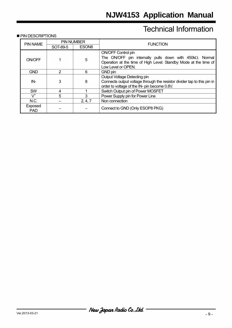
PIN DESCRIPTIONS
PIN NUMBER PIN NAME SOT-89-5 ESON8 FUNCTION
ON/OFF 1 5
ON/OFF Control pin The ON/OFF pin internally pulls down with 450kΩ. Normal Operation at the time of High Level. Standby Mode at the time of Low Level or OPEN.
GND 2 6 GND pin
IN- 3 8 Output Voltage Detecting pin Connects output voltage through the resistor divider tap to this pin in order to voltage of the IN- pin become 0.8V.
SW 4 1 Switch Output pin of Power MOSFET V+ 5 3 Power Supply pin for Power Line
N.C. – 2, 4, 7 Non connection Exposed
PAD – – Connect to GND (Only ESOP8 PKG)
Technical Information
NJW4153 Application Manual
NJW4153
- 10 - Ver.2013-03-21
Description of Block Features
1. Basic Functions / Features Error Amplifier Section (ER⋅AMP)
0.8V±1% precise reference voltage is connected to the non-inverted input of this section. To set the output voltage, connects converter's output to inverted input of this section (IN- pin). If requires output
voltage over 0.8V, inserts resistor divider. Because the optimized compensation circuit is built-in, the application circuit can be composed of minimum
external parts. PWM Comparator Section (PWM), Oscillation Circuit Section (OSC)
The NJW4153 uses a constant frequency, current mode step down architecture. The oscillation frequency is 1,000kHz (typ.) at A version. The PWM signal is output by feedback of output voltage and slope compensation switching current at the PWM comparator block.
The maximum duty ratio is 90% (typ.). The minimum ON time is limited to 140nsec (typ.). The buck converter of ON time is decided the following formula.
[ ]sfV
VtonOSCIN
OUT
×=
VIN shows input voltage and VOUT shows output voltage. When the ON time becomes below in tON-min, in order to maintain output voltage at a stable state, change of duty or
pulse skip operation may be performed. Power MOSFET (SW Output Section)
The power is stored in the inductor by the switch operation of built-in power MOSFET. The output current is limited to 1.4A(min.) the overcurrent protection function. In case of step-down converter, the forward direction bias voltage is generated with inductance current that flows into the external regenerative diode when MOSFET is turned off.
The SW pin allows voltage between the V+ pin and the SW pin up to +45V. However, you should use an Schottky diode that has low saturation voltage.
Power Supply, GND pin (V+ and GND)
In line with switching element drive, current flows into the IC according to frequency. If the power supply impedance provided to the power supply circuit is high, it will not be possible to take advantage of IC performance due to input voltage fluctuation. Therefore insert a bypass capacitor close to the V+ pin – the GND pin connection in order to lower high frequency impedance.
Technical Information
NJW4153 Application Manual
NJW4153
- 11 -Ver.2013-03-21
Description of Block Features (Continued)
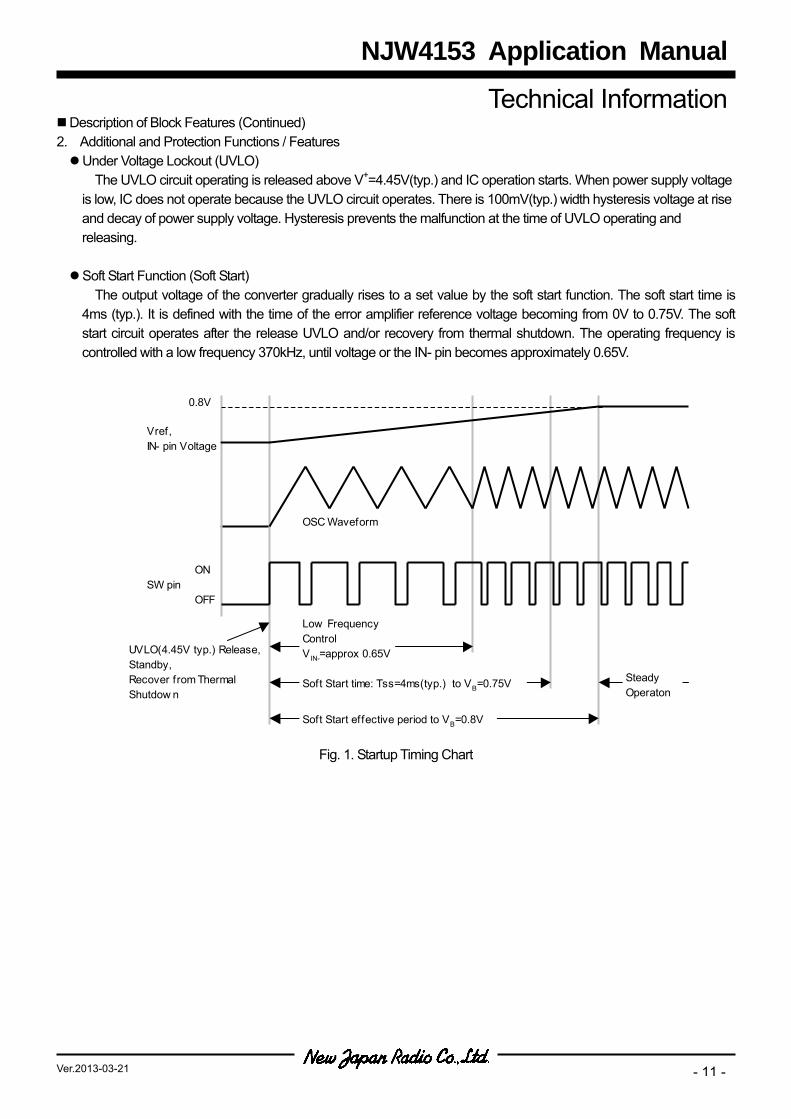
2. Additional and Protection Functions / Features Under Voltage Lockout (UVLO)
The UVLO circuit operating is released above V+=4.45V(typ.) and IC operation starts. When power supply voltage is low, IC does not operate because the UVLO circuit operates. There is 100mV(typ.) width hysteresis voltage at rise and decay of power supply voltage. Hysteresis prevents the malfunction at the time of UVLO operating and releasing.
Soft Start Function (Soft Start)
The output voltage of the converter gradually rises to a set value by the soft start function. The soft start time is 4ms (typ.). It is defined with the time of the error amplifier reference voltage becoming from 0V to 0.75V. The soft start circuit operates after the release UVLO and/or recovery from thermal shutdown. The operating frequency is controlled with a low frequency 370kHz, until voltage or the IN- pin becomes approximately 0.65V.
SW pin
0.8V
ON
OFF
Vref,IN- pin Voltage
OSC Waveform
SteadyOperaton
UVLO(4.45V typ.) Release,Standby,Recover from ThermalShutdow n
Soft Start effective period to VB=0.8V
Soft Start time: Tss=4ms(typ.) to VB=0.75V
Low FrequencyControlVIN-=approx 0.65V
Fig. 1. Startup Timing Chart
Technical Information
NJW4153 Application Manual
NJW4153
- 12 - Ver.2013-03-21
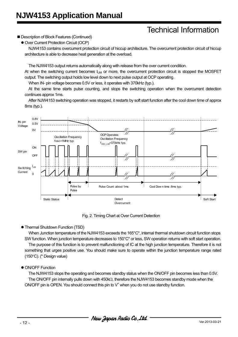
Description of Block Features (Continued) Over Current Protection Circuit (OCP)
NJW4153 contains overcurrent protection circuit of hiccup architecture. The overcurrent protection circuit of hiccup architecture is able to decrease heat generation at the overload.
The NJW4153 output returns automatically along with release from the over current condition.
At when the switching current becomes ILIM or more, the overcurrent protection circuit is stopped the MOSFET output. The switching output holds low level down to next pulse output at OCP operating.
When IN- pin voltage becomes 0.5V or less, it operates with 370kHz (typ.). At the same time starts pulse counting, and stops the switching operation when the overcurrent detection
continues approx 1ms. After NJW4153 switching operation was stopped, it restarts by soft start function after the cool down time of approx
8ms (typ.).
SW pinON
OFF
Sw itchingCurrent
ILIM
0
0.8V0.5V
0V
IN- pinVoltage
OCP OperatesOscillation FrequencyfOSC_LIM=370kHz typ.
Cool Dow n time :8ms typ.
Oscillation Frequencyfosc=1MHz typ.
Static Status DetectOvercurrent
Soft Start
Pulse byPulse
Pulse Count :about 1ms
Fig. 2. Timing Chart at Over Current Detection Thermal Shutdown Function (TSD)
When Junction temperature of the NJW4153 exceeds the 165°C*, internal thermal shutdown circuit function stops SW function. When junction temperature decreases to 150°C* or less, SW operation returns with soft start operation.
The purpose of this function is to prevent malfunctioning of IC at the high junction temperature. Therefore it is not something that urges positive use. You should make sure to operate within the junction temperature range rated (150°C). (* Design value)
ON/OFF Function
The NJW4153 stops the operating and becomes standby status when the ON/OFF pin becomes less than 0.5V. The ON/OFF pin internally pulls down with 450kΩ, therefore the NJW4153 becomes standby mode when the
ON/OFF pin is OPEN. You should connect this pin to V+ when you do not use standby function.
Technical Information
NJW4153 Application Manual
NJW4153
- 13 -Ver.2013-03-21
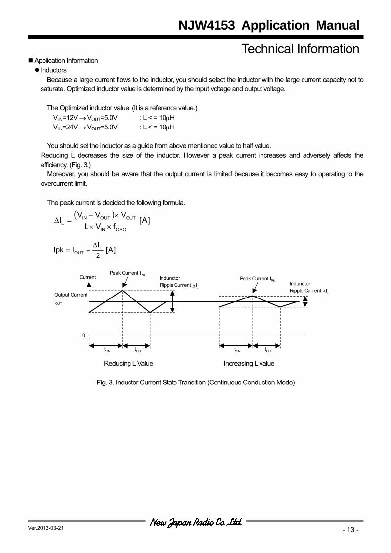
Application Information Inductors
Because a large current flows to the inductor, you should select the inductor with the large current capacity not to saturate. Optimized inductor value is determined by the input voltage and output voltage.
The Optimized inductor value: (It is a reference value.)
ViIN=12V → VOUT=5.0V : L < = 10µH ViIN=24V → VOUT=5.0V : L < = 10µH
You should set the inductor as a guide from above mentioned value to half value.
Reducing L decreases the size of the inductor. However a peak current increases and adversely affects the efficiency. (Fig. 3.)
Moreover, you should be aware that the output current is limited because it becomes easy to operating to the overcurrent limit.
The peak current is decided the following formula.
( )]A[
fVLVVV
IOSCIN
OUTOUTINL ××
×−=∆
]A[I
IIpk LOUT 2
∆+=
Output CurrentIOUT
IndunctorRipple Current ∆IL
0
Current
tON tOFF
Peak Current IPK
IndunctorRipple Current ∆IL
Peak Current IPK
tON tOFF
Reducing L Value Increasing L value
Fig. 3. Inductor Current State Transition (Continuous Conduction Mode)
Technical Information
NJW4153 Application Manual
NJW4153
- 14 - Ver.2013-03-21
Application Information (Continued) Catch Diode
When the switch element is in OFF cycle, power stored in the inductor flows via the catch diode to the output capacitor. Therefore during each cycle current flows to the diode in response to load current. Because diode's forward saturation voltage and current accumulation cause power loss, a Schottky Barrier Diode (SBD), which has a low forward saturation voltage, is ideal.
An SBD also has a short reverse recovery time. If the reverse recovery time is long, through current flows when the switching transistor transitions from OFF cycle to ON cycle. This current may lower efficiency and affect such factors as noise generation.
Input Capacitor
Transient current flows into the input section of a switching regulator responsive to frequency. If the power supply impedance provided to the power supply circuit is large, it will not be possible to take advantage of the NJW4153 performance due to input voltage fluctuation. Therefore insert an input capacitor as close to the MOSFET as possible. A ceramic capacitor is the optimal for input capacitor.
The effective input current can be expressed by the following formula.
( )]A[
VVVV
IIIN
OUTINOUTOUTRMS
−××=
In the above formula, the maximum current is obtained when VIN = 2 × VOUT, and the result in this case is IRMS = IOUT (MAX) ÷ 2.
When selecting the input capacitor, carry out an evaluation based on the application, and use a capacitor that has adequate margin.
Output Capacitor
An output capacitor stores power from the inductor, and stabilizes voltage provided to the output. Because NJW4153 corresponds to the output capacitor of low ESR, the ceramic capacitor is the optimal for compensation.
The Optimized capacitor value: (It is a reference value.) VOUT =5.0V : COUT > = 22µF
In addition, you should consider varied characteristics of capacitor (a frequency characteristic, a temperature
characteristic, a DC bias characteristic and so on) and unevenness peculiar to a capacitor supplier enough. Therefore when selecting a capacitors, you should confirm the characteristics with supplier datasheets. When selecting an output capacitor, you must consider Equivalent Series Resistance (ESR) characteristics, ripple
current, and breakdown voltage.
The output ripple noise can be expressed by the following formula.
]V[IESRV L)pp(ripple ∆×=−
The effective ripple current that flows in a capacitor (Irms) is obtained by the following equation.
]Arms[I
I Lrms
32∆
=
Technical Information
NJW4153 Application Manual
NJW4153
- 15 -Ver.2013-03-21
Application Information (Continued) Setting Output Voltage, Compensation Capacitor
The output voltage VOUT is determined by the relative resistances of R1, R2. The current that flows in R1, R2 must be a value that can ignore the bias current that flows in ER AMP.
]V[VRRV BOUT ×⎟
⎠⎞
⎜⎝⎛ += 1
12
The zero points are formed with R2 and CFB, and it makes for the phase compensation of NJW4153.
The zero point is shown the following formula.
]Hz[CR
fFB
Z ××π×=
221
1
You should set the zero point as a guide from 30kHz to 50kHz.
Technical Information
NJW4153 Application Manual
NJW4153
- 16 - Ver.2013-03-21
Application Information (Continued) Board Layout
In the switching regulator application, because the current flow corresponds to the oscillation frequency, the substrate (PCB) layout becomes an important.
You should attempt the transition voltage decrease by making a current loop area minimize as much as possible. Therefore, you should make a current flowing line thick and short as much as possible. Fig.4. shows a current loop at step-down converter. Especially, should lay out high priority the loop of CIN-SW-SBD that occurs rapid current change in the switching. It is effective in reducing noise spikes caused by parasitic inductance.
COUT
L
SBDCINVIN COUT
L
SBDCINVIN
NJW4153Built-in SW
NJW4153Built-in SW
(a) Buck Converter SW ON (b) Buck Converter SW OFF
Fig. 4. Current Loop at Buck Converter
Concerning the GND line, it is preferred to separate the power system and the signal system, and use single
ground point. The voltage sensing feedback line should be as far away as possible from the inductance. Because this line has
high impedance, it is laid out to avoid the influence noise caused by flux leaked from the inductance. Fig. 5. shows example of wiring at buck converter. Fig. 6 shows the PCB layout example.
SW
GND
IN-
CFB
R2
COUT
L
SBD
NJW4153
R1
VOUT
RL
To avoid the influence of the voltagedrop, the output voltage should bedetected near the load.
Because IN- pin is high impedance, thevoltage detection resistance: R1/R2 isput as much as possible near IC(IN-).
Separate Digital(Signal)GND from Pow er GND
V+
CINVIN
The condenser isconnected near an IC.
Fig. 5. Board Layout at Buck Converter
Technical Information
NJW4153 Application Manual
NJW4153
- 17 -Ver.2013-03-21
Application Information (Continued)
CIN1
CFBRFB
R1
R2
VOUT
Power GND Area
Feed backsignal
GNDOUT
GND IN
VIN
Signal GND Area
CIN2
ON/OFF
SBD
L
COUT
1pin
Connect Signal GND line and Power GND line on backside pattern
Fig. 6. Layout Example (upper view)
Technical Information
NJW4153 Application Manual
NJW4153
- 18 - Ver.2013-03-21
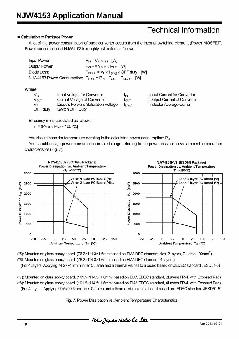
Calculation of Package Power
A lot of the power consumption of buck converter occurs from the internal switching element (Power MOSFET). Power consumption of NJW4153 is roughly estimated as follows.
Input Power: PIN = VIN × IIN [W] Output Power: POUT = VOUT × IOUT [W] Diode Loss: PDIODE = VF × IL(avg) × OFF duty [W] NJW4153 Power Consumption: PLOSS = PIN − POUT − PDIODE [W]
Where:
VIN : Input Voltage for Converter IIN : Input Current for Converter VOUT : Output Voltage of Converter IOUT : Output Current of Converter VF : Diode's Forward Saturation Voltage IL(avg) : Inductor Average Current OFF duty : Switch OFF Duty
Efficiency (η) is calculated as follows.
η = (POUT ÷ PIN) × 100 [%]
You should consider temperature derating to the calculated power consumption: PD. You should design power consumption in rated range referring to the power dissipation vs. ambient temperature
characteristics (Fig. 7).
(*5): Mounted on glass epoxy board. (76.2×114.3×1.6mm:based on EIA/JDEC standard size, 2Layers, Cu area 100mm2) (*6): Mounted on glass epoxy board. (76.2×114.3×1.6mm:based on EIA/JDEC standard, 4Layers)
(For 4Layers: Applying 74.2×74.2mm inner Cu area and a thermal via hall to a board based on JEDEC standard JESD51-5) (*7): Mounted on glass epoxy board. (101.5×114.5×1.6mm: based on EIA/JEDEC standard, 2Layers FR-4, with Exposed Pad) (*8): Mounted on glass epoxy board. (101.5×114.5×1.6mm: based on EIA/JEDEC standard, 4Layers FR-4, with Exposed Pad)
(For 4Layers: Applying 99.5×99.5mm inner Cu area and a thermal via hole to a board based on JEDEC standard JESD51-5)
Fig. 7. Power Dissipation vs. Ambient Temperature Characteristics
Technical Information
NJW4153 Application Manual
NJW4153KV1 (ESON8 Package)Power Dissipation vs. Ambient Temperature
(Tj=~150°C)
0
500
1000
1500
2000
2500
3000
-50 -25 0 25 50 75 100 125 150Ambient Temperature Ta (°C)
Pow
er D
issi
patio
n P
D (
mW
)
At on 4 layer PC Board (*8)At on 2 layer PC Board (*7)
NJW4153U2 (SOT89-5 Package)Power Dissipation vs. Ambient Temperature
(Tj=~150°C)
0
500
1000
1500
2000
2500
3000
-50 -25 0 25 50 75 100 125 150Ambient Temperature Ta (°C)
Pow
er D
issi
patio
n P
D (
mW
)
At on 4 layer PC Board (*6)At on 2 layer PC Board (*5)
NJW4153
- 19 -Ver.2013-03-21
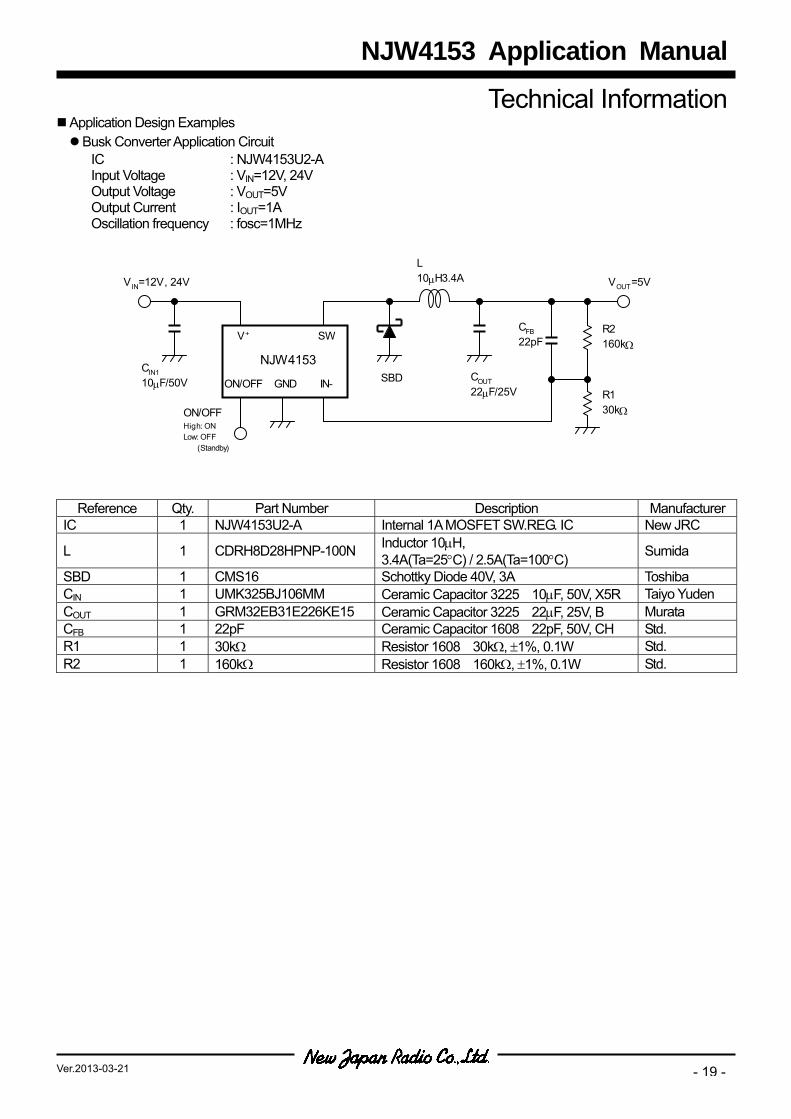
Application Design Examples Busk Converter Application Circuit
IC Input Voltage
: NJW4153U2-A : VIN=12V, 24V
Output Voltage : VOUT=5V Output Current : IOUT=1A Oscillation frequency : fosc=1MHz
SW
GND IN-
V+
NJW4153
ON/OFF SBD
VIN=12V, 24V
CFB22pF
R2160kΩ
R130kΩ
COUT22µF/25V
L10µH3.4A
CIN110µF/50V
VOUT=5V
ON/OFFHigh: ONLow: OFF (Standby)
Reference Qty. Part Number Description ManufacturerIC 1 NJW4153U2-A Internal 1A MOSFET SW.REG. IC New JRC
L 1 CDRH8D28HPNP-100N Inductor 10µH, 3.4A(Ta=25°C) / 2.5A(Ta=100°C) Sumida
SBD 1 CMS16 Schottky Diode 40V, 3A Toshiba CIN 1 UMK325BJ106MM Ceramic Capacitor 3225 10µF, 50V, X5R Taiyo Yuden COUT 1 GRM32EB31E226KE15 Ceramic Capacitor 3225 22µF, 25V, B Murata CFB 1 22pF Ceramic Capacitor 1608 22pF, 50V, CH Std. R1 1 30kΩ Resistor 1608 30kΩ, ±1%, 0.1W Std. R2 1 160kΩ Resistor 1608 160kΩ, ±1%, 0.1W Std.
Technical Information
NJW4153 Application Manual
NJW4153
- 20 - Ver.2013-03-21
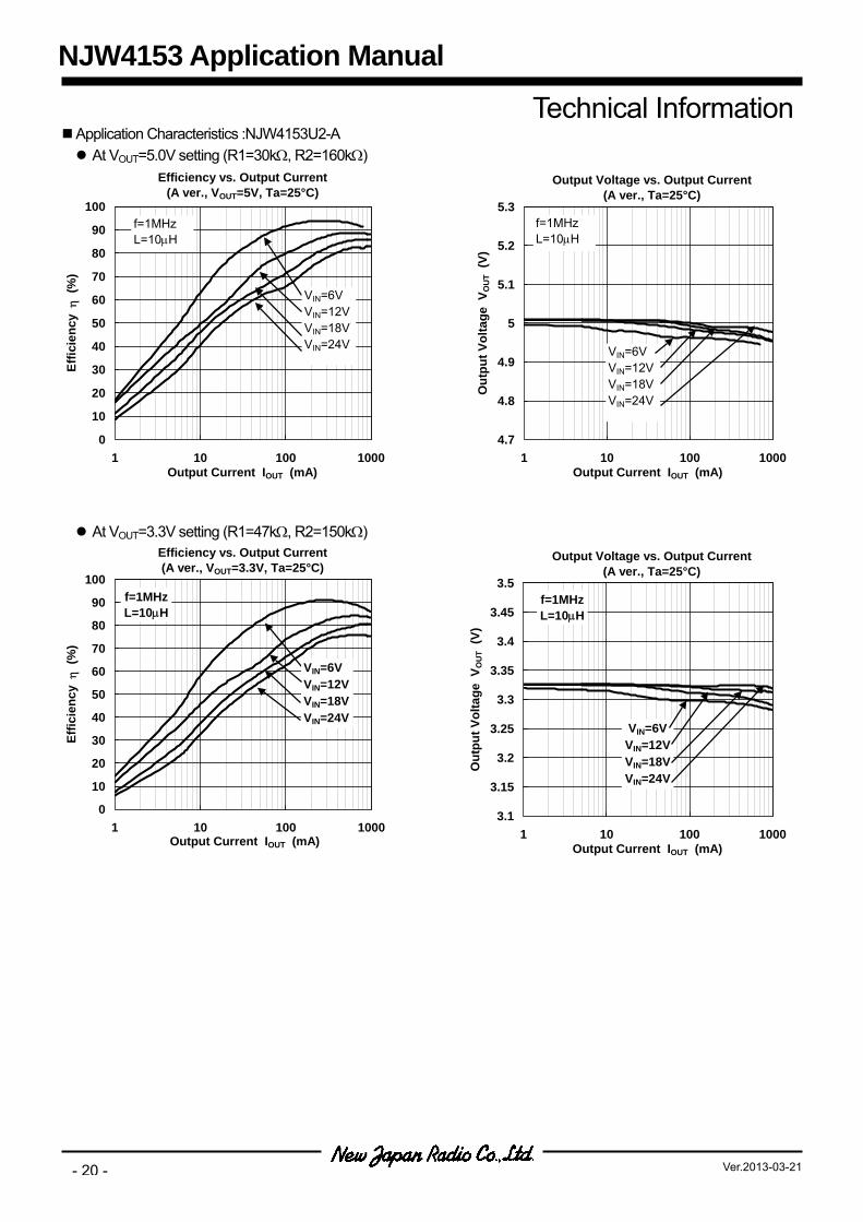
Application Characteristics :NJW4153U2-A At VOUT=5.0V setting (R1=30kΩ, R2=160kΩ)
At VOUT=3.3V setting (R1=47kΩ, R2=150kΩ)
Technical Information
NJW4153 Application Manual
Efficiency vs. Output Current(A ver., VOUT=5V, Ta=25°C)
0
10
20
30
40
50
60
70
80
90
100
1 10 100 1000Output Current IOUT (mA)
Effic
ienc
y η
(%
)
f=1MHzL=10µH
VIN=6VVIN=12VVIN=18VVIN=24V
Output Voltage vs. Output Current(A ver., Ta=25°C)
4.7
4.8
4.9
5
5.1
5.2
5.3
1 10 100 1000Output Current IOUT (mA)
Out
put V
olta
ge V
OU
T (V
)
VIN=6VVIN=12VVIN=18VVIN=24V
f=1MHzL=10µH
Efficiency vs. Output Current(A ver., VOUT=3.3V, Ta=25°C)
0
10
20
30
40
50
60
70
80
90
100
1 10 100 1000Output Current IOUT (mA)
Effic
ienc
y η
(%
)
f=1MHzL=10µH
VIN=6VVIN=12VVIN=18VVIN=24V
Output Voltage vs. Output Current(A ver., Ta=25°C)
3.1
3.15
3.2
3.25
3.3
3.35
3.4
3.45
3.5
1 10 100 1000Output Current IOUT (mA)
Out
put V
olta
ge V
OU
T (V
)
VIN=6VVIN=12VVIN=18VVIN=24V
f=1MHzL=10µH
NJW4153
- 21 -Ver.2013-03-21
Inverting Converter Application Circuit
SW
GND IN-
V+
NJW4153
ON/OFF
SBD
ON/OFFHigh: ONLow: OFF (Standby)
CFBOptional
R1910kΩ
L10µH/3.4A
VIN=15V
CIN10µF/50V R2
51kΩ
VOUT= -15V
COUT22µF/25V
CC0.47µF/50V
Reference Qty. Part Number Description ManufacturerIC 1 NJW4153U2-A Internal 1A MOSFET SW.REG. IC New JRC
L 1 CDRH8D28HPNP-100N Inductor 10µH, 3.4A(Ta=25°C) / 2.5A(Ta=100°C) Sumida
SBD 1 CMS16 Schottky Diode 40V, 3A Toshiba CIN 1 UMK325BJ106MM Ceramic Capacitor 3225 10µF, 50V, X5R Taiyo Yuden COUT 1 GRM32EB31E226KE15 Ceramic Capacitor 3225 22µF, 25V, B Murata CC 1 GRM21BB31H474KA87 Ceramic Capacitor 2012 0.47µF, 50V, B Murata CFB 0 ⎯ (Optional) Optional ⎯ R1 1 910kΩ Resistor 1608 910kΩ, ±1%, 0.1W Std. R2 1 51kΩ Resistor 1608 51kΩ, ±1%, 0.1W Std.
Technical Information
Efficiency vs. Output Current(A ver. , VIN=15V, VOUT=-15V, Ta=25°C)
0
10
20
30
40
50
60
70
80
90
100
1 10 100 1000Output Current IOUT (mA)
Effic
ienc
y η
(%
)
f=1MHzL=10µH
Output Voltage vs. Output Current(A ver. , VIN=15V, Ta=25°C)
-17.0
-16.5
-16.0
-15.5
-15.0
-14.5
-14.0
-13.5
-13.01 10 100 1000
Output Cuurent IOUT (mA)
Out
put V
olta
ge V
OU
T (V
)
f=1MHzL=10µH

NJW4153
- 22 - Ver.2013-03-21
MEMO
[CAUTION] The specifications on this databook are only
given for information , without any guarantee as regards either mistakes or omissions. The application circuits in this databook are described only to show representative usages of the product and not intended for the guarantee or permission of any right including the industrial rights.