Embed Size (px)
Citation preview

European Association for the Development of Renewable Energies, Environment and Power Quality
International Conference on Renewable Energies and Power Quality (ICREPQ’09)
Valencia (Spain), 15th to 17th April, 2009
Performance analysis of three-phase PWM rectifiers for high power quality applications
J. A. A. Caseiro1, A. M. S. Mendes2
University of Coimbra, FCTUC/IT Department of Electrical and Computer Engineering
Pólo II – Pinhal de Marrocos, P – 3030-290, Coimbra, Portugal Phone: +351 239 796232, Fax: +351 239 796247, e-mail: [email protected], [email protected]
Abstract – New power quality issues have brought new concerns about how the electrical devices connected to the mains behave and how their behaviour affects the mains quality and, consequently, other energy consumers. In result of these recent concerns, various new standards were made to limit the harmonic pollution that each device may produce. Diode rectifiers are one of the main polluters, not complying with these standards. The necessity for alternatives reaffirmed PWM rectifiers as a viable alternative. PWM additional capabilities as unity power factor and energy regeneration are other advantages that can be decisive in certain applications. This paper compares diode and PWM rectifiers. It analyses the performance of these systems and explores the PWM systems’ new capabilities. A Matlab/Simulink model has been made to allow the comparison. Simulation results are then verified by laboratorial implementation of the model. Simulation and experimental results are presented and commented. Key words Rectifier, PWM, SVPWM, SPWM, Harmonic, Power Quality
1. Introduction In the past few years problems like harmonic pollution or waveform distortion became more important as the load nature changed. The typical linear loads have been progressively replaced by non-linear ones, where rectifier systems have a great importance. A wide variety of industrial applications such as variable speed drives and most of power electronic converters use uncontrolled rectifiers as a primary stage of the conversion. The highly distorted currents absorbed by these systems may result in voltage distortion, which spreads the problem to other equipments or even to other energy consumers [1],[2]. High distortion levels bring several problems as increased losses in cables and other equipment resulting in overheating, control equipment malfunction, increased failure risk due to resonance situations, sporadic circuit
breakers erratic functioning, power factor’s correction capacitors destruction and several other problems. Besides, the distortion of the waveform implies the lowering of the power factor, which results in higher current levels than strictly necessary and, in most cases, in the need of correction to avoid extra taxation by the power company [1]-[4]. Additionally, as the concerns with harmonic pollution increased, new standards came up limiting both the harmonic pollution present in the mains voltage and the current harmonics produced by a load [5]. These standards impose limits that diode rectifiers could never comply with. In result, many systems require power filters to minimize the effects of the rectifiers. These additional costs made PWM rectifiers, despite being more expensive, a reasonable alternative. Since rectifier systems have such a great responsibility in the problem, development of alternatives and solutions became a priority. PWM rectifiers answered the necessity for alternatives, bringing new capabilities to rectification. Although they require a relatively complex control, due to the possibility to control the semiconductor devices’ conduction state, they have many advantages as low input current distortion, controllable power factor operation, controllable DC voltage, low ripple DC voltage and regenerative capabilities [1]-[4]. These characteristics make PWM rectifiers the best choice in high quality applications. The control of PWM rectifiers can be made in numerous ways and the generation of the control impulses can also be accomplished using diverse modulation strategies. Two of them are the Sinusoidal PWM (SPWM), where a fixed frequency carrier is used to generate the impulses, and Space Vector PWM (SVPWM), where the concept of Space Vector is used to generate the impulses in an optimal way [6]-[11]. This paper compares a diode rectifier with a PWM rectifier, analysing the impact of each one of them in the
https://doi.org/10.24084/repqj07.388 468 RE&PQJ, Vol. 1, No.7, April 2009
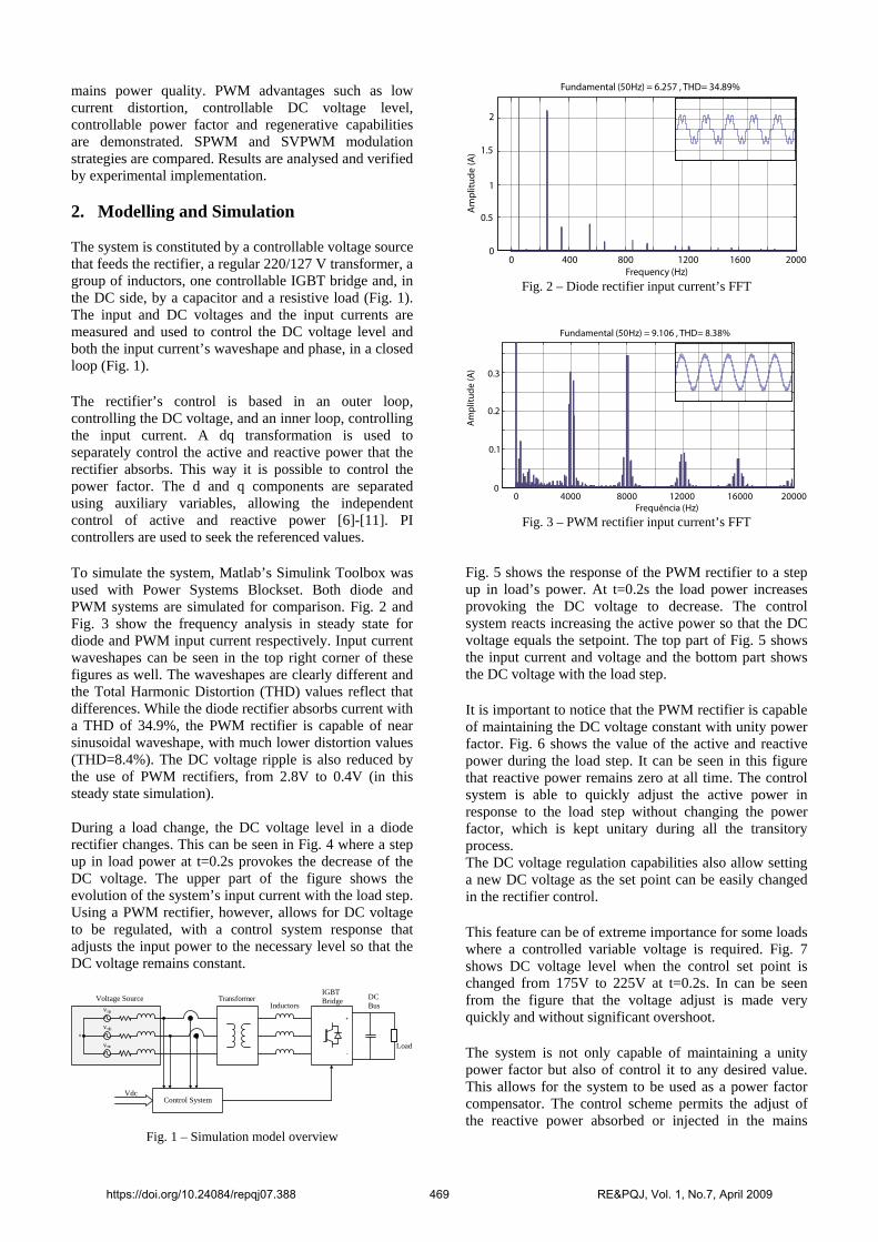
mains power quality. PWM advantages such as low current distortion, controllable DC voltage level, controllable power factor and regenerative capabilities are demonstrated. SPWM and SVPWM modulation strategies are compared. Results are analysed and verified by experimental implementation. 2. Modelling and Simulation The system is constituted by a controllable voltage source that feeds the rectifier, a regular 220/127 V transformer, a group of inductors, one controllable IGBT bridge and, in the DC side, by a capacitor and a resistive load (Fig. 1). The input and DC voltages and the input currents are measured and used to control the DC voltage level and both the input current’s waveshape and phase, in a closed loop (Fig. 1). The rectifier’s control is based in an outer loop, controlling the DC voltage, and an inner loop, controlling the input current. A dq transformation is used to separately control the active and reactive power that the rectifier absorbs. This way it is possible to control the power factor. The d and q components are separated using auxiliary variables, allowing the independent control of active and reactive power [6]-[11]. PI controllers are used to seek the referenced values. To simulate the system, Matlab’s Simulink Toolbox was used with Power Systems Blockset. Both diode and PWM systems are simulated for comparison. Fig. 2 and Fig. 3 show the frequency analysis in steady state for diode and PWM input current respectively. Input current waveshapes can be seen in the top right corner of these figures as well. The waveshapes are clearly different and the Total Harmonic Distortion (THD) values reflect that differences. While the diode rectifier absorbs current with a THD of 34.9%, the PWM rectifier is capable of near sinusoidal waveshape, with much lower distortion values (THD=8.4%). The DC voltage ripple is also reduced by the use of PWM rectifiers, from 2.8V to 0.4V (in this steady state simulation). During a load change, the DC voltage level in a diode rectifier changes. This can be seen in Fig. 4 where a step up in load power at t=0.2s provokes the decrease of the DC voltage. The upper part of the figure shows the evolution of the system’s input current with the load step. Using a PWM rectifier, however, allows for DC voltage to be regulated, with a control system response that adjusts the input power to the necessary level so that the DC voltage remains constant.
vna
vnb
vnc
n
+
-
IGBTBridge
Load
TransformerInductors
DCBus
Voltage Source
Control SystemVdc
Fig. 1 – Simulation model overview
0 400 800 1200 1600 20000
0.5
1
1.5
2
Frequency (Hz)
Fundamental (50Hz) = 6.257 , THD= 34.89%
Am
plitu
de(A
)
Fig. 2 – Diode rectifier input current’s FFT
0 4000 8000 12000 16000 200000
0.1
0.2
0.3
Frequência (Hz)
Fundamental (50Hz) = 9.106 , THD= 8.38%
Am
plitu
de(A
)
Fig. 3 – PWM rectifier input current’s FFT
Fig. 5 shows the response of the PWM rectifier to a step up in load’s power. At t=0.2s the load power increases provoking the DC voltage to decrease. The control system reacts increasing the active power so that the DC voltage equals the setpoint. The top part of Fig. 5 shows the input current and voltage and the bottom part shows the DC voltage with the load step. It is important to notice that the PWM rectifier is capable of maintaining the DC voltage constant with unity power factor. Fig. 6 shows the value of the active and reactive power during the load step. It can be seen in this figure that reactive power remains zero at all time. The control system is able to quickly adjust the active power in response to the load step without changing the power factor, which is kept unitary during all the transitory process. The DC voltage regulation capabilities also allow setting a new DC voltage as the set point can be easily changed in the rectifier control. This feature can be of extreme importance for some loads where a controlled variable voltage is required. Fig. 7 shows DC voltage level when the control set point is changed from 175V to 225V at t=0.2s. In can be seen from the figure that the voltage adjust is made very quickly and without significant overshoot. The system is not only capable of maintaining a unity power factor but also of control it to any desired value. This allows for the system to be used as a power factor compensator. The control scheme permits the adjust of the reactive power absorbed or injected in the mains
https://doi.org/10.24084/repqj07.388 469 RE&PQJ, Vol. 1, No.7, April 2009

allowing for the compensation of other equipments’ reactive power and improving the global power factor.
0.1 0.15 0.2 0.25 0.3
186
190
194
198
202
Time (s)
Volta
ge(V
)
-1.5
-0.5
0.5
1.5
Volta
ge/C
urre
nt (P
U)
VoltageCurrent
Fig. 4 – Input current and voltage and DC voltage in
load step situation (diode rectifier)
0.1 0.15 0.2 0.25 0.3196
198
200
202
Time(s)
Volta
ge(V
)
-1.5
-0.5
0.5
1.5
Volta
ge/C
urre
nt (P
U)
VoltageCurrent
Fig. 5 - Input current and voltage and DC voltage in
load step situation (PWM rectifier)
0.1 0.15 0.2 0.25 0.3-0.5
0
0.5
1
1.5
2
2.5
Time (s)
P/Q
(kW
/kVA
r)
PQ
Fig. 6 – Active and reactive power during
load step (PWM rectifier)
0.1 0.15 0.2 0.25 0.3170
180
190
200
210
220
230
Time (s)
Volta
ge(V
)
Fig. 7 – DC voltage when the control DC voltage
set point is changed.
0.1 0.15 0.2 0.25 0.3-1.5
-1
-0.5
0
0.5
1
1.5
Time(s)
Volta
ge/C
urre
nt (P
U)
VoltageCurrent
Fig. 8 – Input voltage and current when
reactive power set point is changed The maximum active power in this situation is limited by the converter’s nominal current. Fig. 8 shows the input voltage and current for a situation where the reactive energy set point is changed from 0 to 2000 VAr at t=0.2s. Fig. 9 shows the evolution of active and reactive power in this situation. The increase in active power is not provoked by a load change but by losses due to the increase of current magnitude. One of the most important features of the PWM system is the capability of energy regeneration. The PWM system has the capability of reversing the power flow, injecting energy back on the grid. This property is indispensable when a regenerative system is projected. The enabling for regenerative braking gives to the PWM system advantage in most traction appliances. When energy is injected in the DC bus, by a regenerative breaking or any other method, the DC voltage tends to rise. The control system responds, draining energy from the DC bus and injecting it in the mains, so that the DC voltage is maintained. The simulated system proved to be capable of regenerative mode functioning when a voltage source, placed in series with the load, injected energy in the DC bus and tried to elevate the DC voltage. Fig. 10, Fig. 11 and Fig. 12 illustrate system’s input voltage and current, active and reactive power and the DC voltage in this situation. The voltage source was turned on at t=0.2s and the system reacts immediately. In this new situation the input current is not in phase with the voltage anymore. Instead, the current is opposing the voltage so that the power flows to the mains (Fig. 10). The power flow inverts direction (so in becomes negative in Fig. 11) so that the DC voltage tends to diminish.
https://doi.org/10.24084/repqj07.388 470 RE&PQJ, Vol. 1, No.7, April 2009

The amount of power drained from the DC bus should be such that ensures the stability of the DC voltage. Fig. 12 show the evolution of the DC voltage in this situation. Simulations using SPWM and SVPWM returned similar results. However, the SVPWM modulation strategy was able to return lower distortion values for the same switching frequency (8.39% against 9.18%). Additionally, SVPWM modulation also allowed lower DC voltage ripple values (0.54V against 0.6V). Although the results of both modulation strategies are similar, the SVPWM returned better results in the simulations.
0.1 0.15 0.2 0.25 0.3-0.5
0
0.5
1
1.5
2
2.5
Time (s)
P/Q
(kW
/kVA
r)
PQ
Fig. 9 – Active and reactive power when the reactive
power set point is changed
0.1 0.15 0.2 0.25 0.3-1.5
-1
-0.5
0
0.5
1
1.5
Time (s)
Volta
ge/C
urre
nt (P
U)
VoltageCurrent
Fig. 10 – Input voltage and current when
regenerative mode is activated
0.1 0.15 0.2 0.25 0.3-0.8
-0.6
-0.4
-0.2
0
0.2
Time (s)
P/Q
(kW
/kVA
r)
PQ
Fig. 11 – Active and reactive power when
regenerative mode is activated
0.1 0.15 0.2 0.25 0.398
100
102
104
106
Time (s)
Volta
ge(V
)
Fig. 12 – DC voltage when regenerative mode is activated
3. Experimental Results The experimental results were obtained using a variable transformer to obtain the desired feeding voltage and a computer with a National Instruments PCI 6071E interface card and a standard parallel port to control the system (Fig. 13). The input currents and voltages and the DC voltage are read by current and voltage Tektronix probes and sent to the computer through the interface card. The computer processes all the control functions and outputs the command signals to the Semikron IGBT bridge through the parallel port. The implementation has some limitations due to the limited capabilities of the physical equipment used. The major of these limitations is the computational step that because of the real time requirements had to be increased (to 100µs instead of 5µs) which greatly compromised the modulation block performance. The current waveshapes will, therefore, have a greater harmonic distortion that will also provoke the greater ripple in the DC voltage. The control system response and the system capabilities, however, are not affected. The system, then, maintains all the previous properties. One of the system’s main properties verified in the simulation was the capability to stabilize the DC voltage against load changes and to regulate the DC voltage value. Fig. 14 and Fig. 15 show the diode and the PWM system’s DC voltage respectively, when a step up in the load power occur.
+
-
IGBTBridge
Load
TransformerBusDC
Interface Card
Vdc
Ia Ib
Va
nV
bn
Control Impulses
Variable Transformer
Vdc*Q*
Fig. 13 – Experimental model overview
https://doi.org/10.24084/repqj07.388 471 RE&PQJ, Vol. 1, No.7, April 2009

0 0.5 1 1.5 2175
180
185
190
195
200
205
Time (s)
Volta
ge(V
)
Fig. 14 – DC voltage when a step in the load
power occurs (diode rectifier)
0 0.5 1 1.5 2180
185
190
195
200
205
210
Time (s)
Volta
ge(V
)
Fig. 15 - DC voltage when a step in the load
power occurs (PWM rectifier) Once again it can be seen that the diode rectifier has no control over the DC voltage, resulting in a voltage drop. The PWM rectifier (Fig. 15) however is capable of controlling the DC voltage keeping it constant during all the time. The increase of the absorbed power required to maintain the DC voltage can be seen through the increase in the input current, shown in Fig. 16. The PWM rectifier permits, additionally, the regulation of the DC voltage set point. Fig. 17 shows the DC bus voltage when the control set point is changed from 185V to 200V at t=1s. The voltage adjust is accomplished rapidly. The PWM system should also have the ability to control the power factor. It should not only be able to work with near unity power factor but also with a controllable power factor. It should even be able to function in a purely capacitive or inductive manner.
1.22 1.24 1.26 1.28 1.3 1.32 1.34 1.36 1.38 1.4-1.5
-1
-0.5
0
0.5
1
1.5
Time (s)
Volta
ge/C
urre
nt (P
U)
VoltageCurrent
Fig. 16 – Input voltage and current when a step in
load power occurs
0 0.5 1 1.5 2170
180
190
200
210
Time (s)
Volta
ge(V
)
Fig. 17 – DC voltage when the set point is changed in
the control system Fig. 18 shows voltage and current waveforms when the reactive energy set point is 1500 VAr and the active load is very small (almost purely inductive functioning). One of the most promising features in the PWM systems is the regenerative capability. Therefore, there was the obvious need of testing this feature experimentally. Due to equipment limitations, however, the system voltages had to be diminished as the voltage source used to inject energy in the DC bus had a limited output voltage. Even so, the power that the voltage source accomplishes to inject in the DC bus is relatively few. Also, as this voltage source does not allow current to flow in both directions, the normal operation mode is not possible while this voltage source is connected. The regenerative tests were, therefore, made in steady state. In these tests the system successfully established the reference voltage and kept it constant while injecting in the mains approximately 355W. Fig. 19 shows the input voltage and current during regenerative mode. Once again, the current opposes the voltage so that the power flows from the DC bus to the mains. The experimental results show the validity of the control scheme and demonstrate the properties of the PWM converters previously referred. The results demonstrate as well the expected behaviour of the system in DC bus voltage adjustability and the capacity to maintain it constant during load changes, in controlling power factor and in regeneration capabilities.
0.9 0.92 0.94 0.96 0.98 1-1.5
-1
-0.5
0
0.5
1
1.5
Time (s)
Vo
ltag
e/C
urr
en
t (P
U)
VoltageCurrent
Fig. 18 – Voltage and current when the PWM rectifier is
working in an almost purely inductive manner
https://doi.org/10.24084/repqj07.388 472 RE&PQJ, Vol. 1, No.7, April 2009

0.9 0.92 0.94 0.96 0.98 1-0.8
-0.6
-0.4
-0.2
0
0.2
0.4
0.6
0.8
Time (s)
Volta
ge/C
urre
nt (P
U)
VoltageCurrent
Fig. 19 – Input voltage and current during regenerative mode
4. Conclusions This work demonstrates the superiority of the PWM rectifier systems over the traditional diode ones. Several operation conditions are analysed and new capacities are explored showing that, although new PWM rectifiers are more expensive, they have superior features not only in energy quality terms but also in applications where diode ones could not be applied, as in energy regeneration. This may justify, in many cases, the price difference. The obtained results prove also the efficiency of the proposed control scheme and the implementability of the system. Presented results also establish SVPWM as the most efficient modulation technique of the two here analysed. Simulation and experimental results demonstrate the properties and capabilities of PWM rectifiers. Simulation Parameters Power source parameters: Phase to phase RMS voltage: 220 V Frequency: 50 Hz Source resistance: 1.011e-3 Ω Source inductance: 32e-6 H Transformer parameters: Nominal Power: 6600 VA Nominal frequency: 50 Hz V1 ph-ph: 220 V R1: 1.2237 Ω L1: 0.0017 H V2 ph-ph: 127 V R2: 0.4078 Ω L2: 5.5179e-4 H Magnetization Resistance: 1.7006e+3 Ω Magnetization reactance: 4.8962 H Inductance value: 20e-6 H DC bus Capacitor value: 1.4e-3 F Load resistance value 1*: 21 Ω Load resistance value 2*: 35 Ω * - Resistance 1 is the normally used load while resistance 2 was used as the initial load resistance in the load change test.
References [1] M. H. Rashid, ”Power Electronics Handbook”, Academic
Press, ISBN: 0125816502, Florida, 2001. [2] T. L. Skvarenina, ”The Power Electronics Handbook”,
CRC Press, ISBN: 0849373360, Indiana, 2001. [3] Mohan, N., Undeland, T. M., Robbins, W. P., ”Power
Electronics - Converters, Applications, and Design”, John Wiley & Sons,ISBN:978-0-471-22693-2 USA, 2003.
[4] Rodriguez, J.R.; Dixon, J.W.; Espinoza, J.R.; Pontt, J.;
Lezana, P., "PWM regenerative rectifiers: state of the art," IEEE Transactions on Industrial Electronics, vol.52, no.1, pp. 5-22, Feb. 2005.
[5] IEC, ”International Standard 61000-3-2”, 2005. [6] Neacsu, D.O., "Vectorial current control techniques for
three-phase AC/DC boost converters," Proceedings of the IEEE International Symposium on Industrial Electronics, ISIE '99, vol.2, no., pp.527-532, 1999.
[7] Taha, M., "Active Rectifier Using DQ Vector Control for
Aircraft Power System," Electric Machines & Drives Conference, 2007. IEMDC '07. IEEE International , vol.2, no., pp.1306-1310, 3-5 May 2007.
[8] B. K. Bose, ”Modern Power Electronics and AC
Drives”,Prentice Hall PTR, ISBN:0130167436, Tennessee, 2002.
[9] Dixon, J.W.; Boon-Teck Ooi, "Indirect current control of
a unity power factor sinusoidal current boost type three-phase rectifier," IEEE Transactions on Industrial Electronics, vol.35, no.4, pp.508-515, Nov 1988.
[10] Verdelho, P., "Voltage type reversible rectifiers control
methods in unbalanced and nonsinusoidal conditions," Industrial Electronics Society, 1998. IECON '98. Proceedings of the 24th Annual Conference of the IEEE , vol.1, no., pp.479-484, 31 Aug-4 Sep 1998.
[11] Konghirun, M., "A Three-Phase Space-Vector Based
PWM Rectifier with Power Factor Control," Power Conversion Conference - Nagoya, 2007. PCC '07 , vol., no., pp.57-61, 2-5 April 2007.
https://doi.org/10.24084/repqj07.388 473 RE&PQJ, Vol. 1, No.7, April 2009