Embed Size (px)
Citation preview
PERFORMANCE EVALUATION OF A MULTI-PORT DC-DC CURRENT
SOURCE CONVERTER FOR HIGH POWER APPLICATIONS
A Thesis
by
BILLY FERRALL YANCEY III
Submitted to the Office of Graduate Studies of Texas A&M University
in partial fulfillment of the requirements for the degree of
MASTER OF SCIENCE
May 2010
Major Subject: Electrical Engineering
PERFORMANCE EVALUATION OF A MULTI-PORT DC-DC CURRENT
SOURCE CONVERTER FOR HIGH POWER APPLICATIONS
A Thesis
by
BILLY FERRALL YANCEY III
Submitted to the Office of Graduate Studies of Texas A&M University
in partial fulfillment of the requirements for the degree of
MASTER OF SCIENCE
Approved by:
Chair of Committee, Mehrdad Ehsani Committee Members, Shankar Bhattacharyya Karen Butler-Purry Mark Holtzapple Head of Department, Costas Georghiades
May 2010
Major Subject: Electrical Engineering
iii
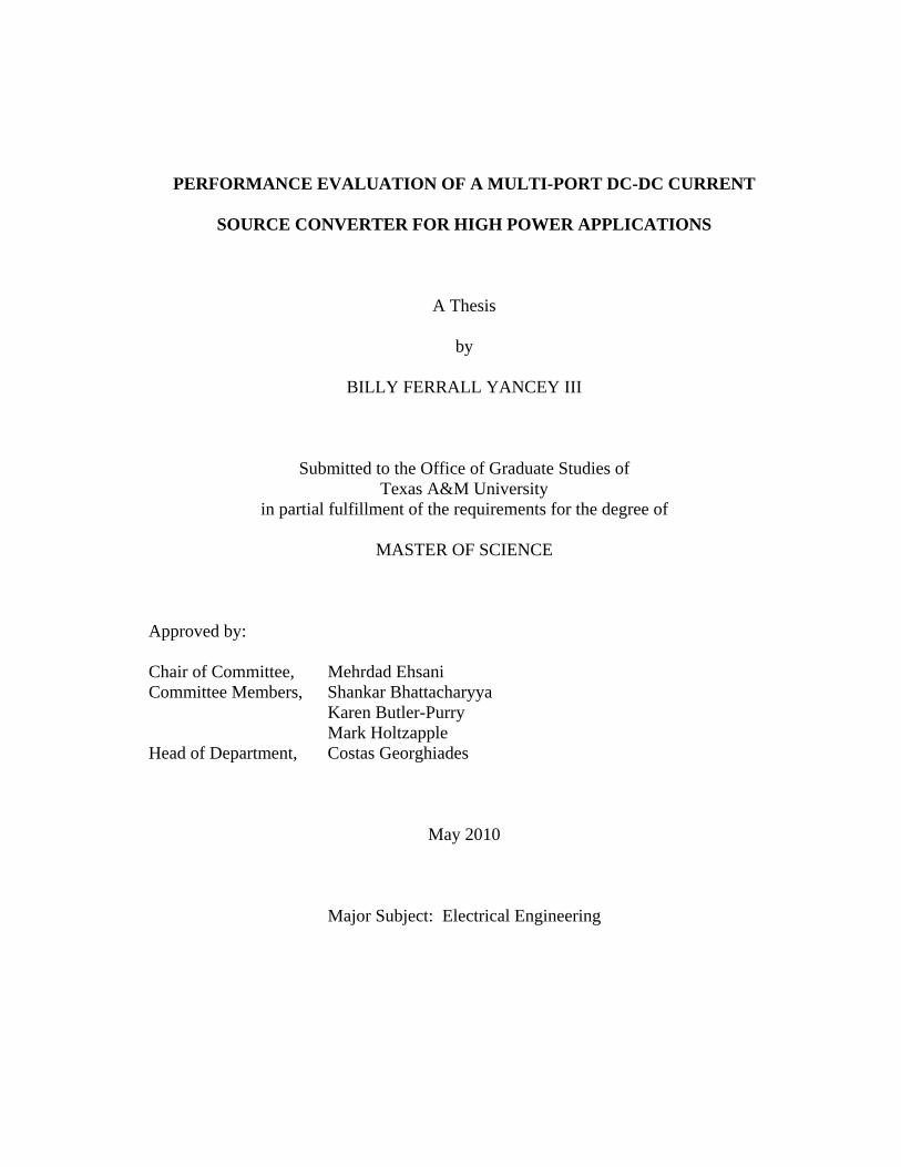
ABSTRACT
Performance Evaluation of a Multi-port DC-DC Current Source Converter for High
Power Applications. (May 2010)
Billy Ferrall Yancey III, B.S.E., Arkansas State University
Chair of Advisory Committee: Dr. Mehrdad Ehsani
With the ever-growing developments of sustainable energy sources such as fuel
cells, photovoltaics, and other distributed generation, the need for a reliable power
conversion system that interfaces these sources is in great demand. In order to provide
the highest degree of flexibility in a truly distributed network, it is desired to not only
interface multiple sources, but to also interface multiple loads. Modern multi-port
converters use high frequency transformers to deliver the different power levels, which
add to the size and complexity of the system. The different topological variations of the
proposed multi-port dc-dc converter have the potential to solve these problems.
This thesis proposes a unique dc-dc current source converter for multi-port power
conversion. The presented work will explain the proposed multi-port dc-dc converter’s
operating characteristics, control algorithms, design and a proof of application. The
converter will be evaluated to determine its functionality and applicability. Also, it will
be shown that our converter has advantages over modern multi-port converters in its ease
of scalability from kW to MW, low cost, high power density and adaption to countless

iv
combinations of multiple sources. Finally we will present modeling and simulation of
the proposed converter using the PSIM® software.
This research will show that this new converter topology is unstable without
feedback control. If the operating point is moved, one of the source ports of the multi-
port converter becomes unstable and dies off supplying very little or no power to the
load while the remaining source port supplies all of the power the load demands. In
order to prevent this and add stability to the converter a simple yet unique control
method was implemented. This control method allowed for the load power demanded to
be shared between the two sources as well as regulate the load voltage about its desired
value.

v
To my parents and my son

vi
ACKNOWLEDGEMENTS
I would like to express my upmost gratitude to Dr. M. Ehsani for his support,
guidance, and words of wisdom throughout the course of my graduate studies. I would
also like to thank all of my committee members for their advice and assistance
throughout this work. I also would like to convey my appreciation to the faculty and
staff of the Electrical Engineering Department at Texas A&M University for their
support and dedication to my education. I want to especially thank all of my current and
former lab members with whom I have spent endless hours, and learned much:
particularly Mr. R. Barazarte, Miss G. Gonzalez, Mr. S. Sarma, and Mr. A. Skorcz. Last
but not least I would like to thank my family, my son, and Miss L. Durham for their
neverending support and encouragement throughout my thesis work and my studies.

vii
TABLE OF CONTENTS
Page
ABSTRACT iii
DEDICATION v
ACKNOWLEDGEMENTS vi
TABLE OF CONTENTS vii
LIST OF FIGURES ix
LIST OF TABLES xiii
CHAPTER
I INTRODUCTION: DC-DC POWER CONVERTERS 1 A. Overview 1 B. Conventional DC-DC Converters 1 C. Multi-port DC-DC Converters 3 1. Multiple Inputs 3 2. Multiple Outputs 4 D. State of the Art Multi-port DC-DC Converters 5 1. Current Source Converters 6 2. Voltage Source Converters 8 E. Summary 9 II PREVIOUS RESEARCH 11 A. Inductor Converter Bridge (ICB) 11 1. Analysis 11 2. Control Techniques 16 3. Multi-port ICB 17 B. Inverse Dual Converter (IDC) 23 1. Analysis 24 2. Control Techniques 28 C. Summary 29

viii
CHAPTER Page III PROPOSED DC-DC CONVERTER TOPOLOGY 30 A. Multi-Source IDC 30 1. Basic Operation and Configuration 31 B. Simulation Study 34 1. Phase Difference Angle Variations 34 2. Input Voltage Deviations 40 3. Load Variations 40 4. System Specifications and Control 41 C. Modeling the System 43 D. Summary 47 IV PERFORMANCE RESULTS, ANALYSIS, AND CONTROL 48
A. Operational Characteristics 48 1. Phase Difference Angle Variation 48 2. Input Voltage Deviation 62 B. Control Results 65 1. Input Voltage Deviation and Load Variation 65 2. Input Voltage Deviation and Load Voltage Variations 68 3. Input Voltage Deviation and Input Current Variations 71 C. Summary 76 V CONCLUSIONS AND FUTURE WORK 77 A. Conclusions 77 B. Future Work 78 REFERENCES 79 APPENDIX A 81 APPENDIX B 88 APPENDIX C 95 APPENDIX D 98 VITA 102

ix
LIST OF FIGURES
FIGURE Page
1 Conventional topology 2
2 Block diagram of a multi-input DC-DC converter 4
3 Block diagram of a multi-output DC-DC converter 5
4 Current source multi-port DC-DC converter 6
5 Multi-port DC-DC converter based on half bridge technique 7
6 Multi-port DC-DC converter based on flux additivity 8
7 Triple-active-bridge DC-DC converter 9
8 Inductor Converter Bridge (ICB) 12
9 Timing diagram of load converter leading storage converter by φ 13
10 Three step phase shift from φ = 0° to φ = -90° 17
11 Multi-port ICB with control variables defined 18
12 PSIM® model of multi-port ICB 20
13 Multi-port ICB source current calculated and simulated 21
14 Multi-port ICB load one current calculated and simulated 22
15 Multi-port ICB load two current calculated and simulated 22
16 Multi-port ICB currents for φ12 ≠ φ13 23
17 Inverse Dual Converter (IDC) 24
18 Symbolic diagram of a gyrator 25
19 Examples of element gyrator transformation 26
x
FIGURE Page
20 Gyrator equivalent IDC viewed from the source 26
21 Gyrator equivalent IDC viewed from the load 27
22 Voltage gain curve 29
23 Multi-source IDC 31
24 Input modules for Sx14 switches conducting 36
25 Input modules for Sx23 switches conducting 37
26 PSIM® model of Multi-source IDC with no controller 45
27 PSIM® model of Multi-source IDC with open loop control 45
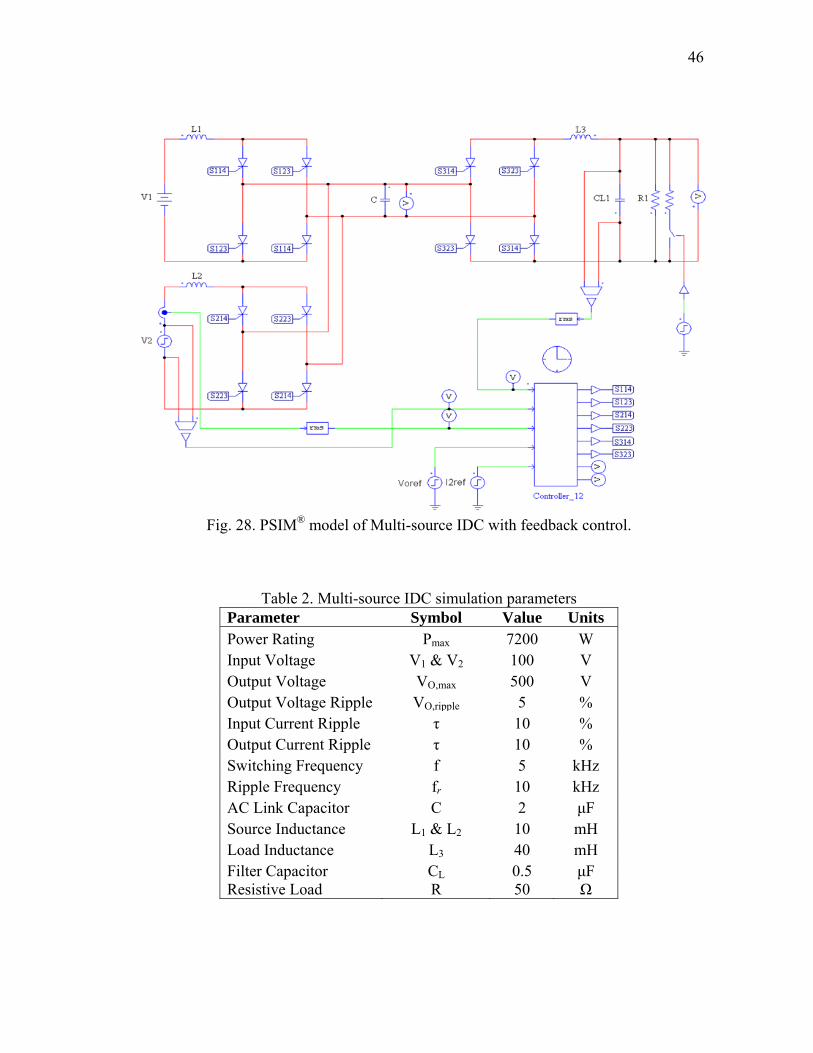
28 PSIM® model of Multi-source IDC with feedback control 46
29 Converter currents for Scenario 1 50
30 Center link capacitor voltage for Scenario 1 50
31 Load voltage for Scenario 1 51
32 Original IDC converter currents 51
33 Magnitude of converter currents for Scenario 1 52
34 Magnitude of load voltage for Scenario 1 52
35 Converter currents for Scenario 2 mode 1 (φ12 = 5°) 54
36 Center link capacitor voltage for Scenario 2 mode 1 (φ12 = 5°) 54
37 Load voltage for Scenario 2 mode 1 (φ12 = 5°) 55
38 Magnitude of converter 1 current for increasing φ12 55
39 Converter currents for Scenario 2 mode 1 (φ12 = 80°) 56
40 Center link capacitor voltage for Scenario 2 mode 1 (φ12 = 80°) 56
xi
FIGURE Page
41 Load voltage for Scenario 2 mode 1 (φ12 = 80°) 57
42 Converter currents for φ12 = 0° to φ12 = 5° 58
43 Center link capacitor voltage for φ12 = 0° to φ12 = 5° 58
44 Load voltage for φ12 = 0° to φ12 = 5° 59
45 Converter currents for φ12 = 0° to φ12 = 45° 60
46 Center link capacitor voltage for φ12 = 0° to φ12 = 45° 61
47 Load voltage for φ12 = 0° to φ12 = 45° 61
48 Converter currents for V2 =25V 62
49 Converter currents for V2 =75V 63
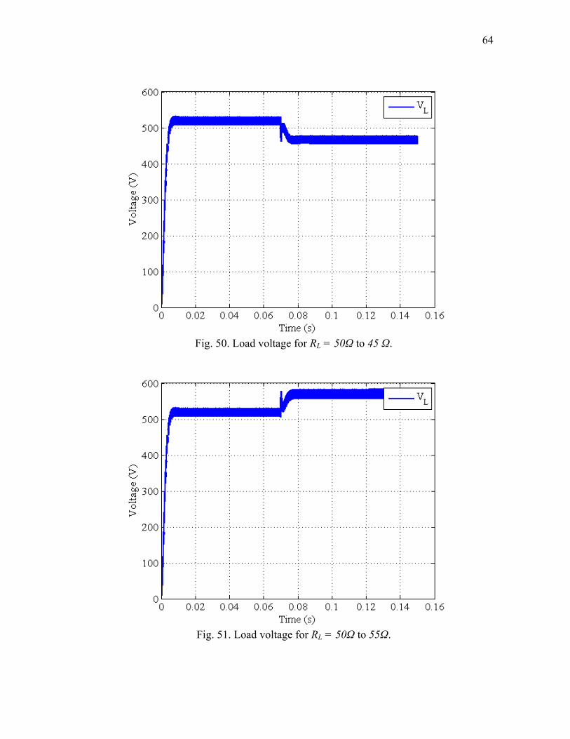
50 Load voltage for RL = 50Ω to 45 Ω 64
51 Load voltage for RL = 50Ω to 55Ω 64
52 Source currents for 10% V2 and 10% RL variations 66
53 Center capacitor voltage for 10% V2 and 10% RL variations 66
54 Load current for 10% V2 and 10% RL variations 67
55 Load voltage for 10% V2 and 10% RL variations 67
56 Phase difference angles for 10% V2 and 10% RL variations 68
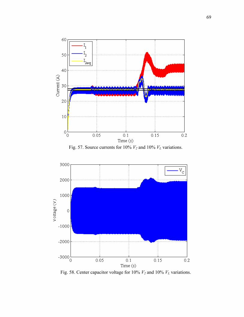
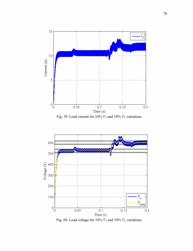
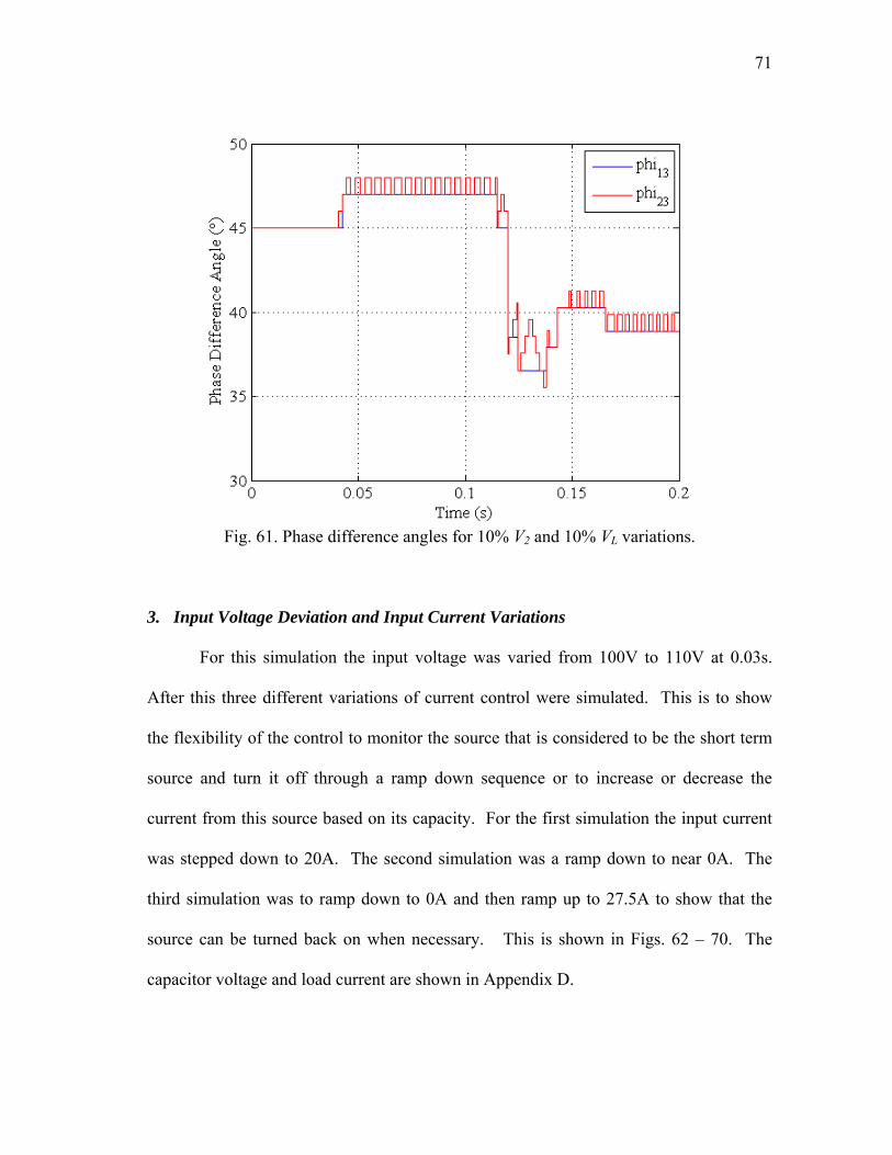
57 Source currents for 10% V2 and 10% VL variations 69
58 Center capacitor voltage for 10% V2 and 10% VL variations 69
59 Load current for 10% V2 and 10% VL variations 70
60 Load voltage for 10% V2 and 10% VL variations 70
61 Phase difference angles for 10% V2 and 10% VL variations 71
xii
FIGURE Page
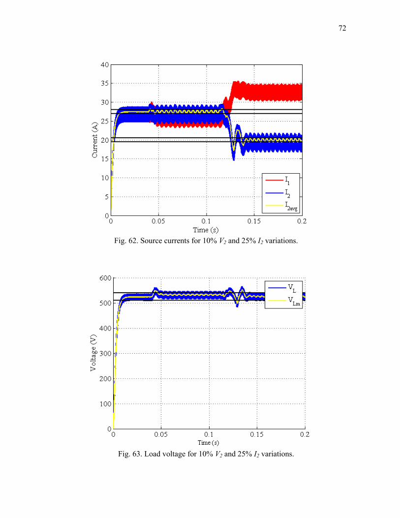
62 Source currents for 10% V2 and 25% I2 variations 72
63 Load voltage for 10% V2 and 25% I2 variations 72
64 Phase difference angles for 10% V2 and 25% I2 variations 73
65 Source currents for 10% V2 and ramp down I2 variations 73
66 Load voltage for 10% V2 and ramp down I2 variations 74
67 Phase difference angles for 10% V2 and ramp down I2 variations 74
68 Source currents for 10% V2 and ramp down and up I2 variations 75
69 Load voltage for 10% V2 and ramp down and up I2 variations 75
70 Phase difference angles for 10% V2 and ramp down/up I2 variations 76

xiii
LIST OF TABLES
TABLE Page
1 Multi-port ICB simulation parameters 20
2 Multi-Source IDC simulation parameters 46
1
CHAPTER I
INTRODUCTION: DC-DC POWER CONVERTERS
This chapter will cover the evolution of multi-port DC-DC converters and their
applications. An overview of multi-port DC-DC converter applications will be
presented along with state of the art topologies being researched. Our research was
motivated by the topics covered in this chapter.
A. Overview
In today’s society the need for renewable energy sources is in high demand.
Over the past few years technological advances have been made in wind power systems,
photovoltaics, fuel cells, and hydroelectric power systems, just to name a few. With
these advances comes the question of how to interface these for standalone power
generation, whether it is one or all of these sources simultaneously. Along with
interfacing multiple inputs, a growing need for interfacing multiple outputs has become
an interesting topic in hybrid vehicles. One way to interface multiple inputs and
multiple outputs is through the use of DC-DC converters.
B. Conventional DC-DC Converters
The first interface systems for renewable energy sources were constructed using
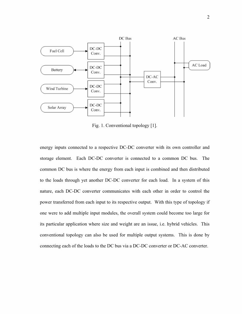
the conventional topology, Fig.1 [1]. The conventional topology consists of multiple
__________ This thesis follows the style and format of the IEEE Transactions on Power Electronics.
2
Fig. 1. Conventional topology [1].
energy inputs connected to a respective DC-DC converter with its own controller and
storage element. Each DC-DC converter is connected to a common DC bus. The
common DC bus is where the energy from each input is combined and then distributed
to the loads through yet another DC-DC converter for each load. In a system of this
nature, each DC-DC converter communicates with each other in order to control the
power transferred from each input to its respective output. With this type of topology if
one were to add multiple input modules, the overall system could become too large for
its particular application where size and weight are an issue, i.e. hybrid vehicles. This
conventional topology can also be used for multiple output systems. This is done by
connecting each of the loads to the DC bus via a DC-DC converter or DC-AC converter.

3
C. Multi-port DC-DC Converters
The multi-port DC-DC converter topology is quickly becoming an alternative for
renewable energy source interfacing [2], [3], [4]. A multi-port converter consists of
multiple inputs or outputs, connected to its respective DC-DC converter. Each DC-DC
converter is then connected to one overall energy storage element, as opposed to
individual storage elements connected to a bus (conventional topology). The control of
each DC-DC converter is then done by one controller to determine amount of power
transferred from each input. This topology is specifically becoming interesting in hybrid
vehicles where there are multiple inputs/outputs [4]. The reason for this interest is
because hybrid vehicles currently have two voltage buses, 14V and 42V. The main bus
is 42V and the 14V bus is then supplied by a DC-DC converter. Multi-level converters
are currently being used to supply these voltages. However, a new bus voltage of 300V
is needed to drive high voltage motor drives for active suspensions [5], and multi-level
converters are not optimal for achieving voltage level differences of this magnitude (14V
to 300V).
1. Multiple Inputs
A multiple input multi-port DC-DC converter is a converter having more than
one energy source as its input. In this topology each input is connected to a DC-DC
converter, then to an individual energy link. The energy link is then connected to
another DC-DC converter, then to the output. A simple block diagram of this is shown
in Fig. 2. A multi-input converter can be a four quadrant, a two quadrant or a single quadrant

4
Fig. 2. Block diagram of a multi-input DC-DC converter.
converter. A four quadrant converter would consist of bidirectional current switches, i.e.
BJTs, IGBTs, etc., and a two quadrant converter would consist of reverse blocking
switches, i.e. SCRs, GTOs, etc. The use of two or four quadrant converters will allow
for the inputs to send and receive power in either quadrants II and III or in all quadrants
respectively. A single quadrant converter (diodes) will only allow power to be sent or
received depending on the connection of the converter. A four quadrant converter can
be useful in systems that have batteries, ultracapacitors, or other types of bidirectional
current storage media. The two quadrant converter is useful in systems that do not
require bidirectional current for storage, i.e. super magnetic energy storage.
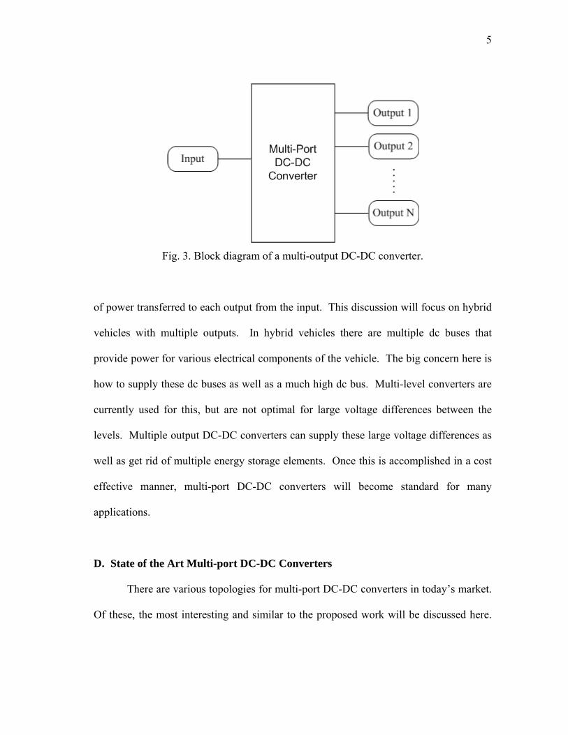
2. Multiple Outputs A multiple output multi-port DC-DC converter is defined as one having multiple
outputs and is shown in Fig. 3. These multiple outputs are connected to an energy link
through its respective DC-DC converter. One controller is used to monitor the amount
5
Fig. 3. Block diagram of a multi-output DC-DC converter.
of power transferred to each output from the input. This discussion will focus on hybrid
vehicles with multiple outputs. In hybrid vehicles there are multiple dc buses that
provide power for various electrical components of the vehicle. The big concern here is
how to supply these dc buses as well as a much high dc bus. Multi-level converters are
currently used for this, but are not optimal for large voltage differences between the
levels. Multiple output DC-DC converters can supply these large voltage differences as
well as get rid of multiple energy storage elements. Once this is accomplished in a cost
effective manner, multi-port DC-DC converters will become standard for many
applications.
D. State of the Art Multi-port DC-DC Converters
There are various topologies for multi-port DC-DC converters in today’s market.
Of these, the most interesting and similar to the proposed work will be discussed here.
6
These converters will be placed into two categories, current source converters and
voltage source converters.
1. Current Source Converters
A current source converter (CSC) is one which determines current at the output
and whose voltage is determined by the load. State of the art CSCs are voltage
controlled current source converters. This means that a voltage source is placed in series
with an inductor in order to simulate a current source. The size of the inductor
determines how stiff the current is over one cycle. The current from this type of input is
determined by the output. If this output is changed and the inductor is large enough the
current will stay constant over one cycle. Therefore making it resemble a current source.
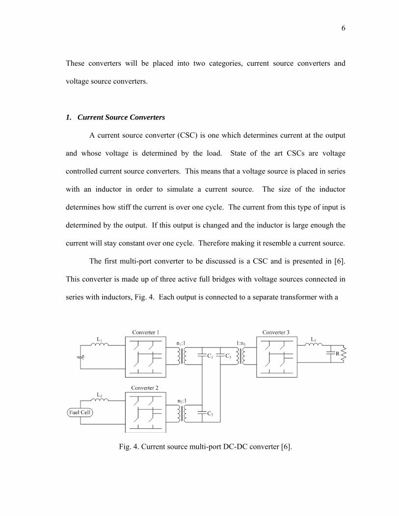
The first multi-port converter to be discussed is a CSC and is presented in [6].
This converter is made up of three active full bridges with voltage sources connected in
series with inductors, Fig. 4. Each output is connected to a separate transformer with a
Fig. 4. Current source multi-port DC-DC converter [6].
7
capacitor across their respective terminals. The power transfer control strategy for this
converter is done by shifting the timing of the bridges, leading or lagging, with respect to
each other in order to transfer power. By adjusting this timing, the amount of power
transferred will be changed. The power from each input is transferred through the
transformer link.
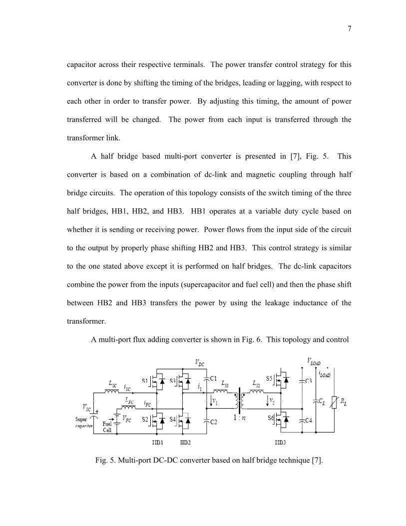
A half bridge based multi-port converter is presented in [7], Fig. 5. This
converter is based on a combination of dc-link and magnetic coupling through half
bridge circuits. The operation of this topology consists of the switch timing of the three
half bridges, HB1, HB2, and HB3. HB1 operates at a variable duty cycle based on
whether it is sending or receiving power. Power flows from the input side of the circuit
to the output by properly phase shifting HB2 and HB3. This control strategy is similar
to the one stated above except it is performed on half bridges. The dc-link capacitors
combine the power from the inputs (supercapacitor and fuel cell) and then the phase shift
between HB2 and HB3 transfers the power by using the leakage inductance of the
transformer.
A multi-port flux adding converter is shown in Fig. 6. This topology and control
Fig. 5. Multi-port DC-DC converter based on half bridge technique [7].
8
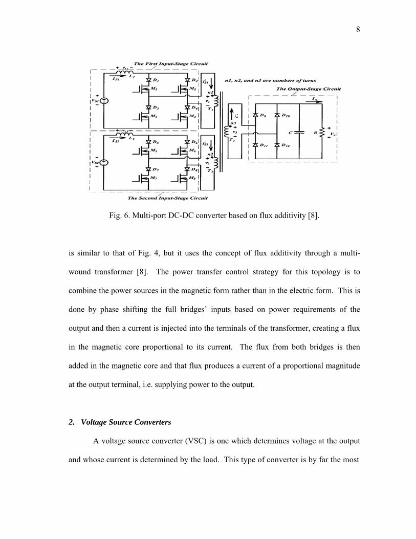
Fig. 6. Multi-port DC-DC converter based on flux additivity [8].
is similar to that of Fig. 4, but it uses the concept of flux additivity through a multi-
wound transformer [8]. The power transfer control strategy for this topology is to
combine the power sources in the magnetic form rather than in the electric form. This is
done by phase shifting the full bridges’ inputs based on power requirements of the
output and then a current is injected into the terminals of the transformer, creating a flux
in the magnetic core proportional to its current. The flux from both bridges is then
added in the magnetic core and that flux produces a current of a proportional magnitude
at the output terminal, i.e. supplying power to the output.
2. Voltage Source Converters
A voltage source converter (VSC) is one which determines voltage at the output
and whose current is determined by the load. This type of converter is by far the most
9
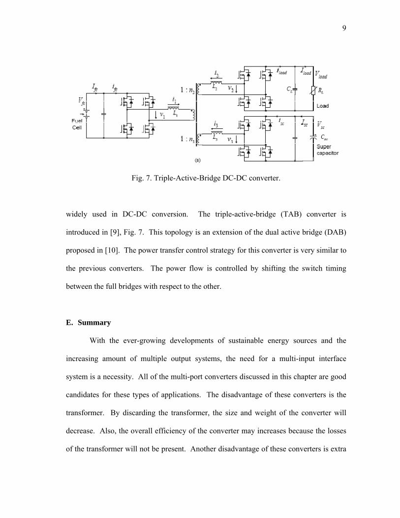
Fig. 7. Triple-Active-Bridge DC-DC converter.
widely used in DC-DC conversion. The triple-active-bridge (TAB) converter is
introduced in [9], Fig. 7. This topology is an extension of the dual active bridge (DAB)
proposed in [10]. The power transfer control strategy for this converter is very similar to
the previous converters. The power flow is controlled by shifting the switch timing
between the full bridges with respect to the other.
E. Summary
With the ever-growing developments of sustainable energy sources and the
increasing amount of multiple output systems, the need for a multi-input interface
system is a necessity. All of the multi-port converters discussed in this chapter are good
candidates for these types of applications. The disadvantage of these converters is the
transformer. By discarding the transformer, the size and weight of the converter will
decrease. Also, the overall efficiency of the converter may increases because the losses
of the transformer will not be present. Another disadvantage of these converters is extra

10
circuitry needed for soft switching. Therefore, a natural soft switching circuit would
decrease the size and weight of the converter without increasing control.

11
CHAPTER II
PREVIOUS RESEARCH
This chapter will describe a family of voltage controlled, current source DC-DC
converters. This family of converters is made up of topological variations of the
Inductor Converter Bridge (ICB) and the Inverse Dual Converter (IDC). This family of
converters is designed specifically for high power applications. The proposed topology,
Multi-source IDC, belongs to this family and will be described in the next chapter. The
objective of this chapter is to give an overview of the different converters in this family
in order to obtain a better understanding of their operational characteristics.
A. Inductor Converter Bridge (ICB)
The ICB, Fig. 7, was originally designed for two quadrant power transfer
between two superconducting magnets, LS and LL [11]. Each superconductive coil is
connected to a full bridge converter made up of SCRs. The output of each bridge is
attached to a high frequency AC capacitor link, which is used to temporarily store the
energy to be transferred between these two superconductive coils. Power is transferred
in this system by controlling the phase difference between the two converters switching
sequences.
1. Analysis
In Fig. 8, the leftmost converter will be identified as the source and the rightmost
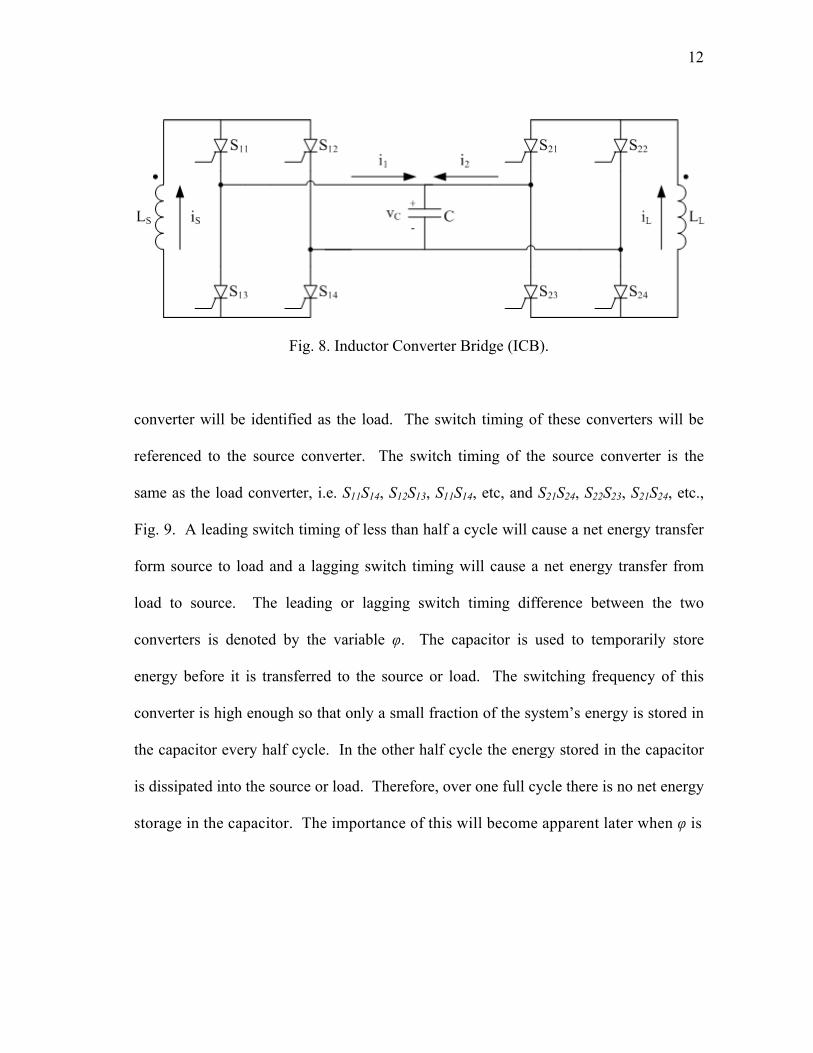
12
Fig. 8. Inductor Converter Bridge (ICB).
converter will be identified as the load. The switch timing of these converters will be
referenced to the source converter. The switch timing of the source converter is the
same as the load converter, i.e. S11S14, S12S13, S11S14, etc, and S21S24, S22S23, S21S24, etc.,
Fig. 9. A leading switch timing of less than half a cycle will cause a net energy transfer
form source to load and a lagging switch timing will cause a net energy transfer from
load to source. The leading or lagging switch timing difference between the two
converters is denoted by the variable φ. The capacitor is used to temporarily store
energy before it is transferred to the source or load. The switching frequency of this
converter is high enough so that only a small fraction of the system’s energy is stored in
the capacitor every half cycle. In the other half cycle the energy stored in the capacitor
is dissipated into the source or load. Therefore, over one full cycle there is no net energy
storage in the capacitor. The importance of this will become apparent later when φ is

13
Fig. 9. Timing diagram of output converter leading input converter by φ.
changed during operation. The capacitor also supplies the reverse voltage necessary for
the commutation of current between the switching events stated above [12].
Dynamic analysis of the ICB has previously been performed by means of fourier
analysis, quadrometrics [12], and state space averaging [13]. The fourier analysis of the
ICB gives an approximate expression for the average power transfer over one cycle from
the source to the load.
1
23sin11
4
n
nLSS n
Cn
IIp
(1)

14
where <pS> is the average source power over one cycle, IS and IL are the average source
and load currents, ω is the angular frequency of the converter and φ is the switch timing
difference between the source and load converters.
State space averaging was used to obtain an averaged solution for the power
transferred within the ICB. The coil currents are shown by the following equations.
LS
S IL
kI (2)
SL
L IL
kI (3)
t
LL
kItI
LS
OS cos (4)
t
LL
k
L
LItI
LSL
SOL sin (5)
where,
C
k
2
(6)
The coil voltages can be obtained from (2) and (3) as

15
LSSS kIILV (7)
SLLL kIILV (8)
The rate of energy leaving the source is defined as positive power,
SSSSSS IILILdt
dp
2
2
1 (9)
Now substituting (2) into (9) we get the average power transferred from source to load is
2
C
IIIkIp LS
LSS (10)
The range of the phase difference angle, φ, is from 0° – 180° depending on the amount
of desired power transfer, but it has been shown in [12] that the power transfer curve is
symmetric about φ = 90°.
Quadrometrics is a mathematical expression of the ICB phase currents as step
functions and the capacitor voltage as a ramp function. Through this rigorous analysis,
which can be seen in detail in [12], the same closed from solution was found for average
power as in (10). Proof that (1) is equal to (10) is shown in [12]. In order to calculate
maximum power transfer, one must take the derivative of (10) with respect to φ and set
equal to zero and solve for φ.
16
2
02
C
II
d
d
d
dp LSS (11)
2. Control Techniques
For the ICB there are two variables that can be controlled to implement power
transfer, phase difference angle φ and switching frequency f [12]. The preferred way to
implement power transfer is through phase modulation because the phase difference
angle φ is the only way one can change the direction of power transfer. When the
amount of power transferred needs to be adjusted some sort of phase shifting is to be
used to prevent overvoltages or voltage imbalances on the capacitor. This can be
performed on either the source or the load converter. Phase shifting should be
implemented in a minimum of a three step shift. For example, if a phase shift of Δφ is to
be implemented the timing sequence is as follows:
211ttt
(12)
212ttt
(13)
13 tt (14)
Note that a Δφ phase shift corresponds to a Δt time shift, Δφ/2πf. Also, note that the
phase angle will be positive for the load converter leading the source converter and vice
versa. Fig. 10 shows that the source converter and load converter are in phase,
17
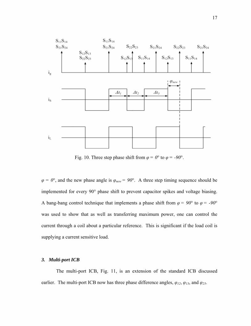
Fig. 10. Three step phase shift from φ = 0° to φ = -90°.
φ = 0°, and the new phase angle is φnew = 90°. A three step timing sequence should be
implemented for every 90° phase shift to prevent capacitor spikes and voltage biasing.
A bang-bang control technique that implements a phase shift from φ = 90° to φ = -90°
was used to show that as well as transferring maximum power, one can control the
current through a coil about a particular reference. This is significant if the load coil is
supplying a current sensitive load.
3. Multi-port ICB
The multi-port ICB, Fig. 11, is an extension of the standard ICB discussed
earlier. The multi-port ICB now has three phase difference angles, φ12, φ13, and φ23.
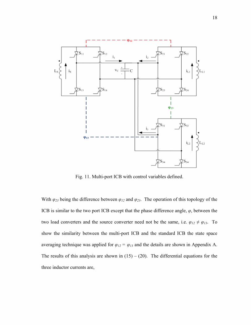
18
Fig. 11. Multi-port ICB with control variables defined.
With φ23 being the difference between φ12 and φ23. The operation of this topology of the
ICB is similar to the two port ICB except that the phase difference angle, φ, between the
two load converters and the source converter need not be the same, i.e. φ12 ≠ φ13. To
show the similarity between the multi-port ICB and the standard ICB the state space
averaging technique was applied for φ12 = φ13 and the details are shown in Appendix A.
The results of this analysis are shown in (15) – (20). The differential equations for the
three inductor currents are,

19
31
21
1 IL
kI
L
kI (15)
12
2 IL
kI (16)
13
3 IL
kI (17)
where k is shown in (6) and through MATLAB’s symbolic solver, the previous
differential equations were solved and are shown in (18) – (20).
t
LLL
LLkII O
321
321 cos (18)
t
LLL
LLk
LLL
LLII O
321
32
322
312 sin (19)
t
LLL
LLk
LLL
LLII O
321
32
323
213 sin (20)
These equations were simulated from t = 0 – 10s and compared with a simulated multi-
port model in PSIM® shown in Fig. 12. The specifications for a predesigned multi-port
ICB are given in Table 1.
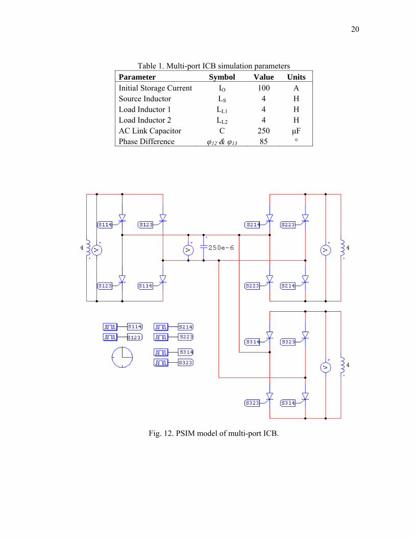
20
Table 1. Multi-port ICB simulation parameters Parameter Symbol Value Units Initial Storage Current IO 100 A Source Inductor LS 4 H Load Inductor 1 LL1 4 H Load Inductor 2 LL2 4 H AC Link Capacitor C 250 μF Phase Difference φ12 & φ13 85 °
Fig. 12. PSIM model of multi-port ICB.
21
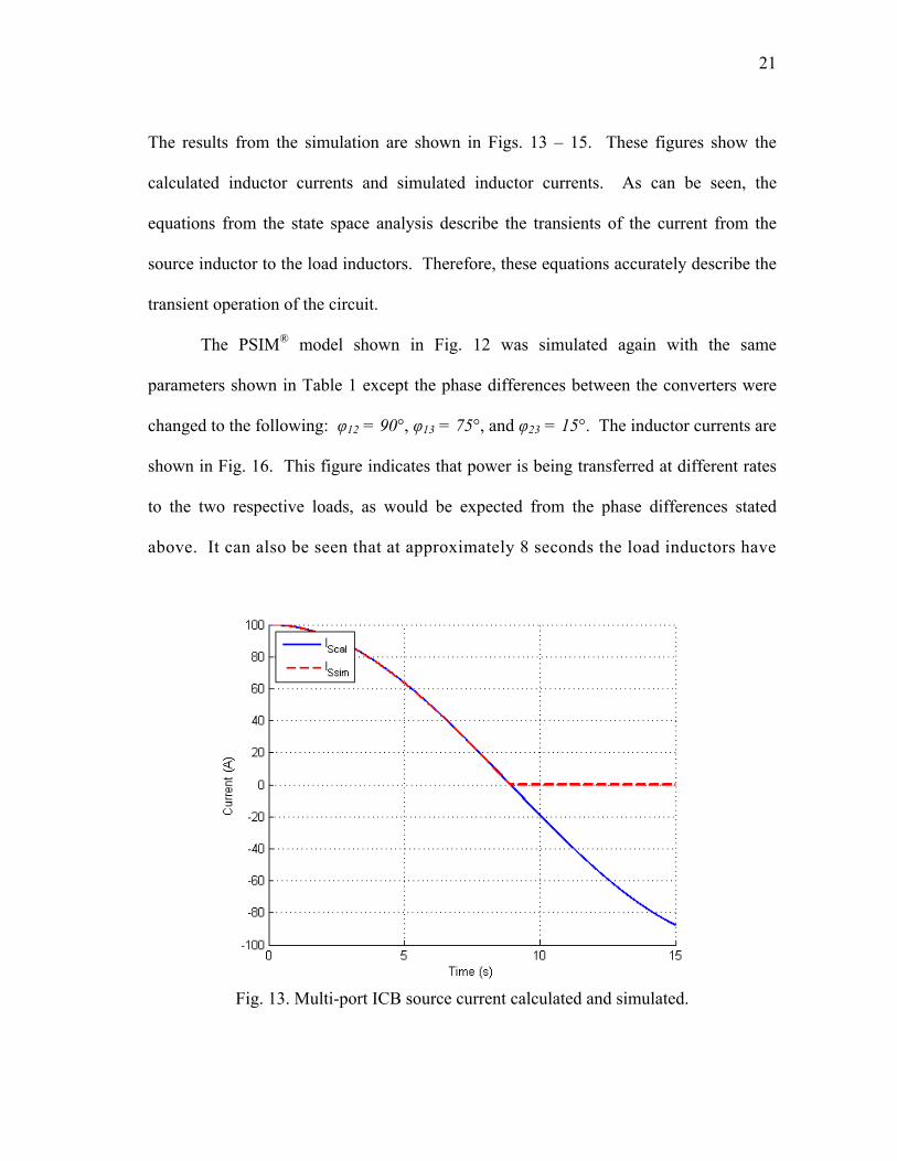
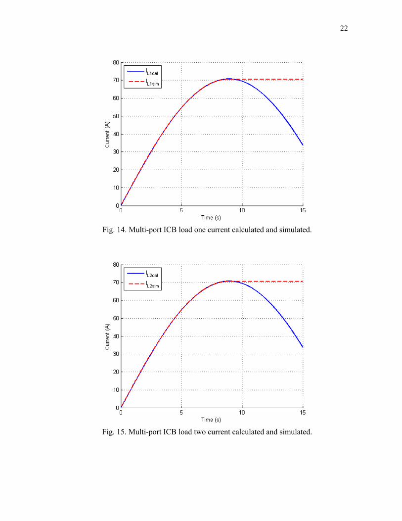
The results from the simulation are shown in Figs. 13 – 15. These figures show the
calculated inductor currents and simulated inductor currents. As can be seen, the
equations from the state space analysis describe the transients of the current from the
source inductor to the load inductors. Therefore, these equations accurately describe the
transient operation of the circuit.
The PSIM® model shown in Fig. 12 was simulated again with the same
parameters shown in Table 1 except the phase differences between the converters were
changed to the following: φ12 = 90°, φ13 = 75°, and φ23 = 15°. The inductor currents are
shown in Fig. 16. This figure indicates that power is being transferred at different rates
to the two respective loads, as would be expected from the phase differences stated
above. It can also be seen that at approximately 8 seconds the load inductors have
Fig. 13. Multi-port ICB source current calculated and simulated.
22
Fig. 14. Multi-port ICB load one current calculated and simulated.
Fig. 15. Multi-port ICB load two current calculated and simulated.
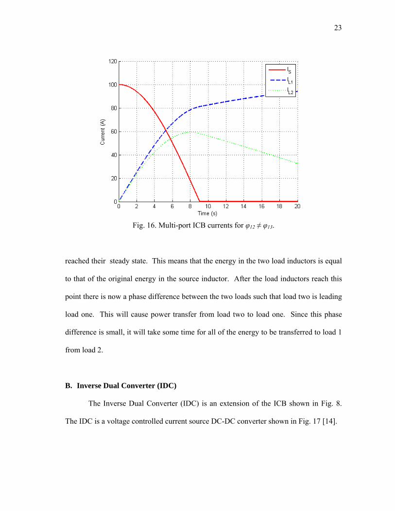
23
Fig. 16. Multi-port ICB currents for φ12 ≠ φ13.
reached their steady state. This means that the energy in the two load inductors is equal
to that of the original energy in the source inductor. After the load inductors reach this
point there is now a phase difference between the two loads such that load two is leading
load one. This will cause power transfer from load two to load one. Since this phase
difference is small, it will take some time for all of the energy to be transferred to load 1
from load 2.
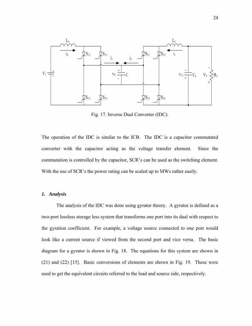
B. Inverse Dual Converter (IDC)
The Inverse Dual Converter (IDC) is an extension of the ICB shown in Fig. 8.
The IDC is a voltage controlled current source DC-DC converter shown in Fig. 17 [14].
24
Fig. 17. Inverse Dual Converter (IDC).
The operation of the IDC is similar to the ICB. The IDC is a capacitor commutated
converter with the capacitor acting as the voltage transfer element. Since the
commutation is controlled by the capacitor, SCR’s can be used as the switching element.
With the use of SCR’s the power rating can be scaled up to MWs rather easily.
1. Analysis
The analysis of the IDC was done using gyrator theory. A gyrator is defined as a
two-port lossless storage less system that transforms one port into its dual with respect to
the gyration coefficient. For example, a voltage source connected to one port would
look like a current source if viewed from the second port and vice versa. The basic
diagram for a gyrator is shown in Fig. 18. The equations for this system are shown in
(21) and (22) [15]. Basic conversions of elements are shown in Fig. 19. These were
used to get the equivalent circuits referred to the load and source side, respectively.

25
Fig. 18. Symbolic diagram of a gyrator.
21 gvi (21)
12 gvi (22)
These circuits are used in the analysis of the IDC to determine source current, load
current, and voltage gain. Now using the IDC model in Fig. 17 and using the gyrator
conversions in Fig. 19 one can obtain two circuits for the IDC. Fig. 20 viewed from the
source side and Fig. 21 viewed from the load side. From Fig. 20 the steady state source
current can be calculated and is
RgV
Rg
VI i
iS
2
2
1 (23)
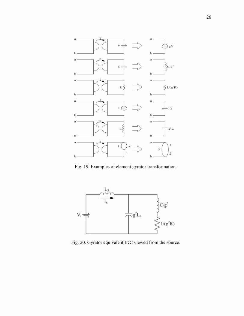
26
Fig. 19. Examples of element gyrator transformation.
Fig. 20. Gyrator equivalent IDC viewed from the source.
27
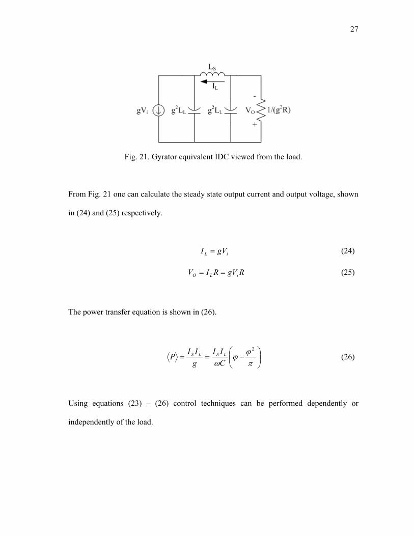
Fig. 21. Gyrator equivalent IDC viewed from the load.
From Fig. 21 one can calculate the steady state output current and output voltage, shown
in (24) and (25) respectively.
iL gVI (24)
RgVRIV iLO (25)
The power transfer equation is shown in (26).
2
C
II
g
IIP LSLS (26)
Using equations (23) – (26) control techniques can be performed dependently or
independently of the load.

28
2. Control Techniques
The control variables for this converter are the same as for the ICB, φ and f. By
adjusting these variables the output voltage and current will be dynamically controlled.
The voltage gain is shown in (27).
RC
gRV
V
i
O
2
(27)
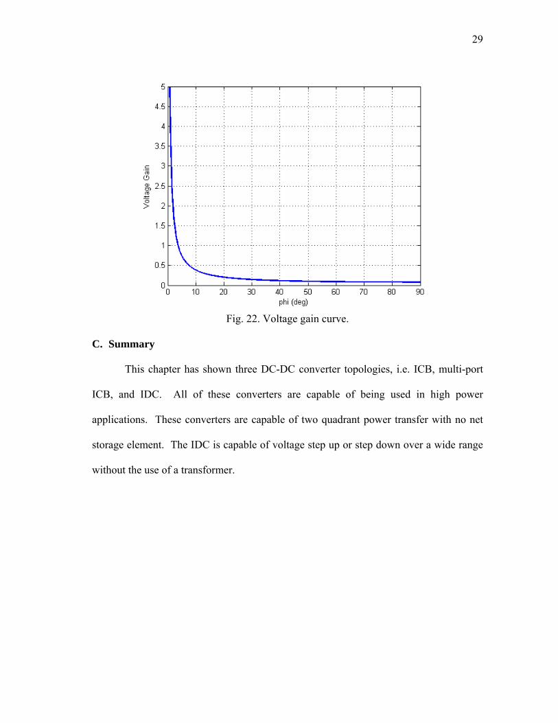
To get a better feel for this equation it was plotted for φ = 0° to φ = 90° for R = 1Ω, Fig.
22. This shows that when φ is chosen to be close to zero the voltage gain becomes
infinite. This is the unstable region of the graph. If a voltage gain in the unstable region
or below the curve is desired the frequency can be dynamically adjusted to shift this
curve up or down. This type of control will not be used in this research. By adjusting φ,
one can only achieve voltages on this curve and it is recommended to stay out of the
unstable region. Also the load resistance is directly proportional to the gain so if it
changes then the overall gain will change. This means that if the output voltage is being
regulated then φ would have to change to bring the gain back to its previous value.
Therefore, the IDC is designed to be able to achieve a certain voltage range within the
stable region of φ.
29
Fig. 22. Voltage gain curve.
C. Summary
This chapter has shown three DC-DC converter topologies, i.e. ICB, multi-port
ICB, and IDC. All of these converters are capable of being used in high power
applications. These converters are capable of two quadrant power transfer with no net
storage element. The IDC is capable of voltage step up or step down over a wide range
without the use of a transformer.

30
CHAPTER III
PROPOSED DC-DC CONVERTER TOPOLOGY
This chapter will discuss a case study performed on the proposed multi-port
power converter. This case study will involve a topological variation of the Inductor
Converter Bridge (ICB) family of converters shown in Chapter II, in particular the
Inverse Dual Converter (IDC). The IDC will be manipulated into a multi-source
converter and various simulation study methods will be presented in this chapter that
will determine various operational characteristics of this converter in order to aid in the
development of a control strategy.
A. Multi-Source IDC
The multi-port IDC is first presented as a multi-load topological variation of the
original IDC in [16]. The multi-port IDC is being expanded into a converter that can
support multiple sources, i.e. Multi-source IDC, Fig. 23. This will allow for multiple
energy sources, renewable or nonrenewable, to be connected and controlled to supply a
load. This will also help in instances where the load power demanded is too great for
just one connection and must be split into two.
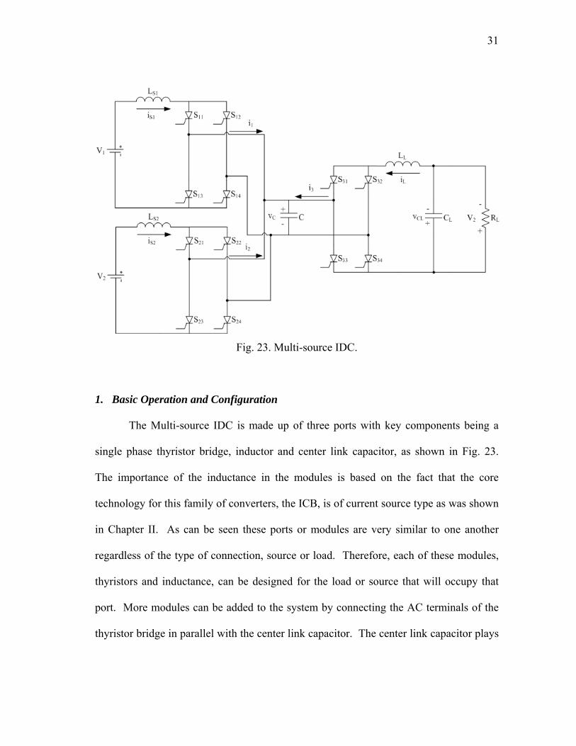
31
Fig. 23. Multi-source IDC.
1. Basic Operation and Configuration
The Multi-source IDC is made up of three ports with key components being a
single phase thyristor bridge, inductor and center link capacitor, as shown in Fig. 23.
The importance of the inductance in the modules is based on the fact that the core
technology for this family of converters, the ICB, is of current source type as was shown
in Chapter II. As can be seen these ports or modules are very similar to one another
regardless of the type of connection, source or load. Therefore, each of these modules,
thyristors and inductance, can be designed for the load or source that will occupy that
port. More modules can be added to the system by connecting the AC terminals of the
thyristor bridge in parallel with the center link capacitor. The center link capacitor plays

32
an important role in this converter by temporarily storing energy every half cycle before
dispersing it to the load. With this know the operation of the Multi-source IDC is very
similar to the IDC with added control for the extra modules added to the system.
As was shown in Chapter II the key variables for power transfer were the phase
difference angle φ and the switching frequency f. For the purpose of this thesis only φ
was manipulated to control the power transfer of the Multi-source IDC. The variable φij
is defined as the difference between the firing angles for the i converter thyristor pair
(αi14 or αi23) and the j converter thyristor pair (αj14 or αj23). If φij is positive then power is
transferred from the i converter to the j converter and if it is negative power is
transferred from the j converter to the i converter. In order to number the converter
modules accordingly a standard top to bottom left to right method will be used. For
instance in Fig. 23, this means that converter 1 is in the top left, converter 2 is in the
bottom left, and converter 3 is in the top right. If there were another converter on the
right then it would be numbered after the top right converter. This means for the
standard IDC presented in Chapter II there is only one phase difference angle where φij=
φji or vice versa depending on the initial firing angles of the respective converters. For
the Multi-source IDC there can be as many phase difference angles as there are ports.
For example in Fig. 23 there is φ13, φ23, and φ12, assuming that the load leads both
sources and that converter 2 leads converter 1. For power transfer to occur the load
converter must lead the source converter. The source port cannot receive power because
the unidirectional switches will not allow for the current to change directions and flow
into the source. Therefore, the only way for the source port to receive power is to
33
reverse the connection of the source such that the current remains in the same direction,
but is fed into the positive terminal of the source which would add complexity.
At first glance the source port of the Multi-source IDC looks like a current source
feeding a capacitor and then feeding a load, but in reality it is a voltage controlled
current source. This means that the voltage at the input has control over the
instantaneous current delivered through the inductor by the equations,
S
CSS
L
vv
dt
di (28)
S
CSS
L
vv
dt
di (29)
where (28) is for a source port whose conducting switches are 1 and 4 and (29) is for
switches 2 and 3 conducting. These equations will cause three different instances during
one half cycle to occur: vS > vC, vS = vC, or vS < vC. For the first of the three instances,
the current in the source inductor will be rising from its previous starting value. This
will continue until the second instance occurs, causing the current to reach its peak value
for that half cycle. Next, the third instance occurs causing the inductor current to fall.
As the current is falling the converter is switched from one pair of switches to the other,
i.e. for converter 1 S114 to S123. For transient periods, like start up and phase shifting, the
starting current in the inductor is different from the final current during the half cycle,
creating a rising or falling net current in the inductor. During these times of operation
the time constant of the switching frequency is faster than the time constant of the
34
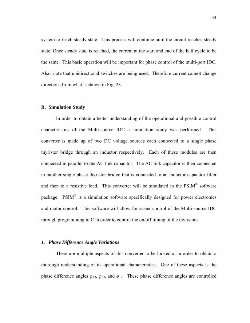
system to reach steady state. This process will continue until the circuit reaches steady
state. Once steady state is reached, the current at the start and end of the half cycle to be
the same. This basic operation will be important for phase control of the multi-port IDC.
Also, note that unidirectional switches are being used. Therefore current cannot change
directions from what is shown in Fig. 23.
B. Simulation Study
In order to obtain a better understanding of the operational and possible control
characteristics of the Multi-source IDC a simulation study was performed. This
converter is made up of two DC voltage sources each connected to a single phase
thyristor bridge through an inductor respectively. Each of these modules are then
connected in parallel to the AC link capacitor. The AC link capacitor is then connected
to another single phase thyristor bridge that is connected to an inductor capacitor filter
and then to a resistive load. This converter will be simulated in the PSIM® software
package. PSIM® is a simulation software specifically designed for power electronics
and motor control. This software will allow for easier control of the Multi-source IDC
through programming in C in order to control the on/off timing of the thyristors.
1. Phase Difference Angle Variations
There are multiple aspects of this converter to be looked at in order to obtain a
thorough understanding of its operational characteristics. One of these aspects is the
phase difference angles φ13, φ23, and φ12. These phase difference angles are controlled

35
by controlling the firing angle of the thyristors between the respective converters as
stated earlier. For the Multi-source IDC the phase difference angle φ can be used to
control how much power each source will send to the load. Therefore, φ13 and φ23 will
be controlled and φ12 is a consequence of these by taking the difference between the two.
The input and load response will be studied by applying the following scenarios for the
phase difference angles mentioned above:
Scenario 1: (φ13 = φ23) > 0 (φ12 = 0)
Scenario 2: φ13 > 0, φ23 > 0 (φ12 > 0 and φ12 < 0)
Scenario 3: φ13 > 0 and φ23 = 0 (φ12 > 0)
Scenario 4: φ13 = 0 and φ23 > 0 (φ12 < 0)
Scenario 5: φ13 > 0 and φ23 < 0 (φ12 > 0)
Scenario 6: φ13 < 0 and φ23 > 0 (φ12 > 0)
Scenario 7: φ13 < 0 and φ23 = 0 (φ12 < 0)
Scenario 8: φ13 = 0 and φ23 < 0 (φ12 > 0)
Scenario 9: φ13 < 0 and φ23 < 0 (φ12 > 0 and φ12 < 0)
These scenario studies were simulated with equal source voltages and a constant
resistive load, i.e. V1 = V2 and RL1 = 50Ω. From above Scenario’s 7 – 9 do make sense
due to the fact that for power transfer to occur the load must be leading at least one of
the sources. Otherwise the load will be required to send power to the sources, which
cannot happen because the voltage source doesn’t change polarity, current direction does
not change, and a resistive load cannot generate power. Scenario’s 3 – 6 also do not
36
make sense and this will be shown during the explanation of Scenario 2. Therefore only
Scenario’s 1 and 2 will be shown in greater detail.
Scenario 1 is the most obvious of all the scenarios with the phase difference
angles equal. Since φ13 = φ23 and both are greater than zero, power will be transferred
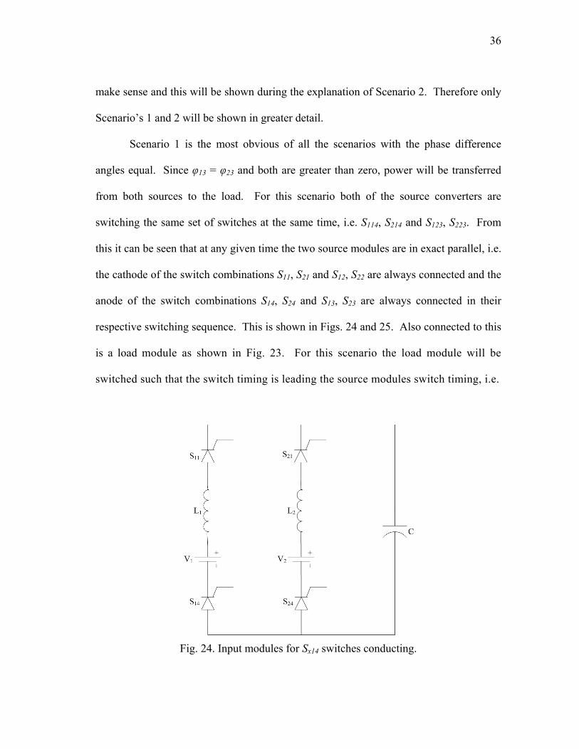
from both sources to the load. For this scenario both of the source converters are
switching the same set of switches at the same time, i.e. S114, S214 and S123, S223. From
this it can be seen that at any given time the two source modules are in exact parallel, i.e.
the cathode of the switch combinations S11, S21 and S12, S22 are always connected and the
anode of the switch combinations S14, S24 and S13, S23 are always connected in their
respective switching sequence. This is shown in Figs. 24 and 25. Also connected to this
is a load module as shown in Fig. 23. For this scenario the load module will be
switched such that the switch timing is leading the source modules switch timing, i.e.
Fig. 24. Input modules for Sx14 switches conducting.
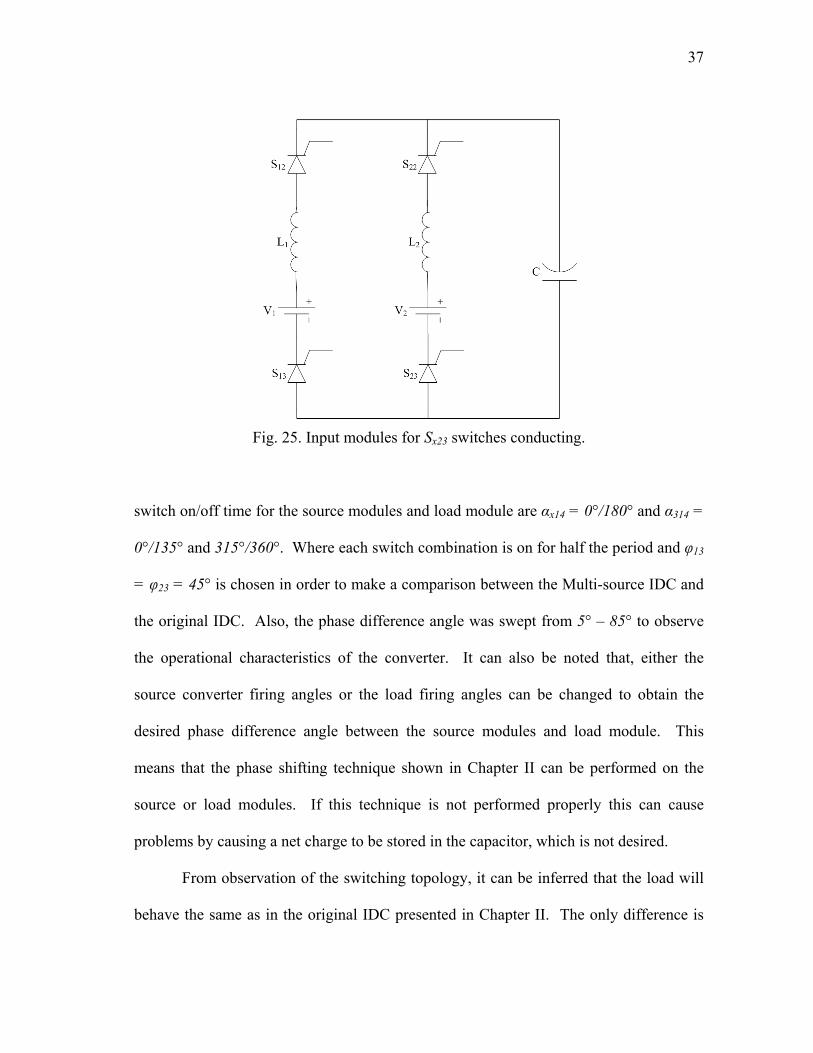
37
Fig. 25. Input modules for Sx23 switches conducting.
switch on/off time for the source modules and load module are αx14 = 0°/180° and α314 =
0°/135° and 315°/360°. Where each switch combination is on for half the period and φ13
= φ23 = 45° is chosen in order to make a comparison between the Multi-source IDC and
the original IDC. Also, the phase difference angle was swept from 5° – 85° to observe
the operational characteristics of the converter. It can also be noted that, either the
source converter firing angles or the load firing angles can be changed to obtain the
desired phase difference angle between the source modules and load module. This
means that the phase shifting technique shown in Chapter II can be performed on the
source or load modules. If this technique is not performed properly this can cause
problems by causing a net charge to be stored in the capacitor, which is not desired.
From observation of the switching topology, it can be inferred that the load will
behave the same as in the original IDC presented in Chapter II. The only difference is
38
that now there are two sources connected in exact parallel at all times. This means for
any given phase difference angle such that φ13 = φ23 the input current will be exactly
split between the two sources. Therefore the same amount of energy is being stored
every half cycle in the capacitor as was for the original IDC case with half coming from
each source. This scenario is considered the most stable operating mode of the Multi-
source IDC and will be used as the basis for conducting the phase shifting technique to
change the phase difference angle of one source module or both source modules
simultaneously. The control and simulations for this scenario will be shown in more
detail in Chapter IV.
Scenario 2 has two different modes that were studied. The first of the two is the
case where (φ13 > φ23) > 0°, making φ12 > 0°. This shows that power is to be transferred
from converter 1 and 2 to converter 3 and from converter 1 to converter 2. As stated
earlier power transfer between source converters cannot occur because the voltage or
current cannot change directions. In order to observe the behavior of this scenario the
firing angle of the load was set at α314 = 0°/180° and α323 = 180°/360° respectively. The
source modules were started at φ12 > 5° with firing angles of α114 = 45°/225° and α214 =
40°/220°. It was observed that the current in module 1 fell to near zero with module 2
carrying the majority of the current to drive the load at φ23 > 40°. This was repeated for
φ12 > 10° by changing α114 = 50°/230°. This showed that the current in module 1 was
even closer to zero and the input of converter 2 and output started to resemble that of the
original IDC presented in Chapter II. The phase difference angle was then swept in 5°
increments in order to observe the lowest average input current of converter 1.

39
The second mode is the case where (φ13 < φ23) > 0°, making φ12 < 0°. This
mode was simulated with φ12 = -5° with firing angles of α114 = 40°/220° and α214 =
45°/225°. Form this simulation it was observed that the exact opposite occurred, i.e.
converter 2 current went to near zero and converter 1 supplies the load. In order to be
complete with the study this mode was simulated the same as the previous. From these
observations it can be determined that if converter 1 leads converter 2, converter 1 will
supply the load alone. If converter 2 leads converter 1 it will supply the load alone. For
control purposes this can be seen as a way to increase or decrease current in either of the
converters.
From this assumption, Scenario’s 3 – 6 can now be shown to make no sense.
Scenario 3 and 4 are similar in that one of the two phase differences is equal to 0°.
Firstly, 0° is an unstable operating point for a single load IDC, therefore in order to make
it semi-stable the point will have to be moved to approximately 10°. Once this is done, it
can be seen that both of these scenarios resemble Scenario 2. Therefore is of no use.
Scenario’s 5 and 6 do not make any sense because of the observations seen in Scenario
2. Both Scenario 5 and 6 have a positive and negative phase difference. From Scenario
2, the converter that is lagging the other converter will go to near zero current. This
means that if the phase difference is negative, the positive phase difference will be
lagging causing it to go to near zero current. Then power is to be transferred from the
load to the source because of the negative phase difference but this cannot happen
because of the reasons mentioned earlier.
40
2. Input Voltage Deviations
To further understand the operation of this converter the input voltages were
made unequal for both Scenario’s 1 and 2. For Scenario 1, converter 2 input voltage was
swept from 25V to 100V in 25V increments. This showed that the larger voltage of
converter 1 caused converter 2 to go to near zero current, i.e. converter 2 has minimal
current with respect to converter 1. The same was shown to happen when the voltage
sweep was performed on converter 1 while keeping converter 2 constant. Further details
on this occurrence will be presented in Chapter IV. This was also done for Scenario 2.
The overall result of this was that if V1 > V2 then converter 1 supplies max current for
the load and converter 2 goes to near zero. The opposite occurs for V1 < V2. This will
be shown in Chapter IV.
3. Load Variations
In most applications the sources load is allowed to vary while continuing to send
it power. If this load is a voltage sensitive load, it is desirable to send power at a fixed
voltage and varying current. In order to do this the load voltage must be regulated for
any change in load. For the Multi-source IDC this load is a simple resistive element. An
increase or decrease of the element should not result in an increase or decrease in output
voltage. If it does then there should be an adjustment to φ13 in order to keep this voltage
within its predetermined range. By knowing how the load voltage varies with increasing
or decreasing RL, φ13 can be adjusted to compensate the voltage back to its desired value.
This is shown in Chapter IV.

41
4. System Specifications and Control
For most systems it is desirable to regulate or control certain characteristics of
the converter, whether it be source current or load voltage during disturbances. The
Multi-source IDC will have two sources, one of which is an unlimited energy source
while the other is limited or determined to be depleting. The load will be a simple
resistive element that will be varied to demonstrate voltage regulation. It is also known
that in most real world applications two sources are never exactly the same, i.e. voltage
variations.
For control of the Multi-source IDC it was decided that the output voltage be
regulated about a particular voltage with a peak to peak hysteresis ripple of 5%. Also,
when one of the sources vary from the other it is not desired that current to go to near
zero values. Therefore, the phase difference angle φ will be adjusted in such a way to
keep the input current of converter 2 about a particular reference with a peak to peak
hysteresis ripple of 5%. Converter 1 will be allowed to send any amount of energy
necessary to supply the load based on the limitations from of converter 2. Since there
are two variables that need to be controlled there needs to be two degrees of freedom.
The control variables will be φ13 and φ23. Since converter 1 is acting like an unlimited
energy source it will be considered the primary control for the system. Since converter 1
will always be available, it will be in charge of the output voltage regulation and
converter 2 will control it power transfer to the load by controlling the current sent to the
load by φ23. Voltage regulation of the load will be a first priority with the current
regulation second. If the load changes while the input current is being regulated, the
42
controller will briefly step out of this routine and compute the new phase difference
angle to meet the voltage criterion. Once this is done, current regulation will continue.
In order to achieve voltage regulation of the output one needs to incorporate a
feedback loop of the output voltage. The instantaneous average voltage is measured and
sent to the controller for comparison with the reference voltage desired. The phase
difference angle φ13 is then adjusted. The algorithm for this is as follows:
refO
Oratio V
V
,
(30)
oldrationew ,13,13 (31)
new,1323 (32)
This set of equations follows the voltage gain curve shown in Chapter II. This shows
that if the measured output voltage rises above or falls below the reference voltage the
phase angle difference will increase or decrease respectively. If this voltage continues to
rise or fall the algorithm will continue to adjust to keep the average voltage within a
hysteresis band of 5%. Also note that φ23 is set equal to φ13 to readjust the base point for
determining current regulation of converter 2.
Current regulation of converter 2 is achieved using a bang-bang type of control.
This type of control changes the control value based on whether the measured value is
above or below the targeted average plus hysteresis band. For this case φ23 will be
increased or decreased depending on if the measured converter 2 current is above or
43
below the hysteresis band respectively. Due to the fact that the load voltage is the first
priority, φ23 is set equal to φ13 every time the output voltage needs to be regulated within
its band. Then φ23 is adjusted around φ13 in order to keep the input current of converter 2
within its operational limits. If converter 2 cannot operate at its predetermined current it
will be reduced or turned off and converter 1 will take over and power the load on its
own. The control logic is as follows:
1,2323,22 oldripref IIIif
1,2323,22 oldripref IIIif
With this logic φ23 will be stepped by one until it reaches a point where it will alternate
between two values. The controller code is presented in Appendix B.
C. Modeling the System
To fully understand the operation of this converter and compare results with past
research, the system and its control was modeled and simulated. Three different
simulation models were developed based on the results to be shown. For a basic
simulation of constant φ over the simulation time the model in Fig. 26 was used. If a
complex control of φ was to be simulated, the model in Fig. 27 was used. If a feedback
control method was used, Fig. 28 was used. A 7.2kW system was designed with an
input voltage (V1 and V2) of 100V and is shown in Figs. 26, 27, and 28. The system
44
components of Figs. 26, 27, and 28 will be designed based on these parameters and the
equations developed in [14] and are shown in (35), (36), and (37).
232
1
fCLS
(35)
232 fC
nLL
(36)
CLr
LL Vf
iC
8
(37)
where
τ is the ripple factor S
S
I
i or
L
L
I
i.
f is the switching frequency.
n is the ratio of average input current divided by average output current.
fr is the ripple frequency.
ΔiL is the peak to peak current in the load.
ΔVCL is the peak to peak voltage in the load capacitor.
From these equations a base model was designed for simulation of this converter and
these component values are shown in Table 2.

45
Fig. 26. PSIM® model of Multi-source IDC with no controller.
Fig. 27. PSIM® model of Multi-source IDC with open loop control.
46
Fig. 28. PSIM® model of Multi-source IDC with feedback control.
Table 2. Multi-source IDC simulation parameters Parameter Symbol Value Units Power Rating Pmax 7200 W Input Voltage V1 & V2 100 V Output Voltage VO,max 500 V Output Voltage Ripple VO,ripple 5 % Input Current Ripple τ 10 % Output Current Ripple τ 10 % Switching Frequency f 5 kHz Ripple Frequency fr 10 kHz AC Link Capacitor C 2 μF Source Inductance L1 & L2 10 mH Load Inductance L3 40 mH Filter Capacitor CL 0.5 μF Resistive Load R 50 Ω

47
D. Summary
This chapter has introduced a new multi-port converter, Multi-source IDC, to
study and analyze. In order to obtain an understanding of its operation, different circuit
variations were studied: phase difference angle variations, input voltage variations, and
load variation. From these studies, control strategies were able to be developed to
regulate the output voltage and converter 2 input current by actively controlling φ13 and
φ23 respectively.
48
CHAPTER IV
PERFORMANCE RESULTS, ANALYSIS, AND CONTROL
In this chapter the simulation results from the Multi-source IDC will be presented
and discussed. All of the simulations presented are based on the specifications discussed
in Chapter III. This chapter will consist of the operational characteristics and control
strategy based on the behavior of the Multi-source IDC.
A. Operational Characteristics
In order to better understand the operational characteristics of the Multi-source
IDC it was simulated under various conditions. These conditions include the variation
of phase difference angle, φ, between each converter, variation of the each source
voltage (V1 and V2), and load variation (RL). From these simulation studies, a control
method can be determined in order to keep the converter at a stable operating point while
maintaining output voltage regulation and converter 2 current regulation. This converter
was simulated in PSIM®.
1. Phase Difference Angle Variation
The first simulation study of this converter consists of directly controlling φ by
controlling the respective firing angles for each converter and switch. These firing
angles are α1XX, α2XX, and α3XX, where XX stands for the switch pair per converter. The
phase difference angle φ between two converters is just the difference of these firing

49
angles. For this simulation, the model shown in Fig. 26 from Chapter III was simulated.
For Scenario 1 α1XX and α2XX are set equal to one another and α3XX was varied in order to
change φ between the two source converters and the load converter. For example, the
firing angles for converters 1 and 3 would be α114 = 0°/180° (on/off) and α314 = 0°/135°
and 315°/360° (on/off and on/off). From these firing angles one can see that the
converter 3 leads converter 1, therefore power will be transferred from converter 1 to
converter 3. Also the phase difference angle for these firing angles is φ13 = 180°-135° =
45°. Fig. 26 was simulated for V1 = V2 = 100V, φ13 = φ23= 45° and φ12 = 0° for a time
of 0.15s at a sample rate of 1E-8s and the converter currents, capacitor voltage, and load
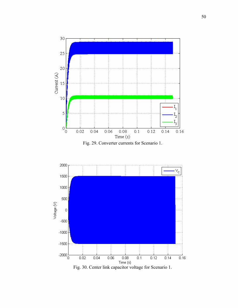
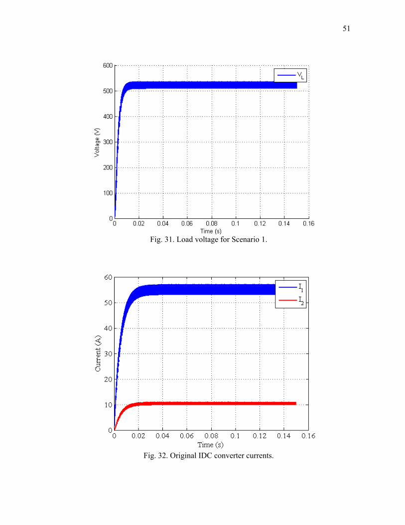
voltage are shown in Figs. 29 – 31.
In Fig. 29 the larger current is both input currents overlapping one another. From
this it was determined that as long as φ13 = φ23 and V1 = V2 or ideal operating conditions
the two sources will exactly split the current of the original IDC shown in Fig. 32. Fig.
30 also shows that the capacitor voltage is not biased with an average over a period
equal to zero. The smaller current in Fig. 29 is the load current and Fig. 31 shows the
load voltage, both of which are the same as the original IDC for the same phase angle
difference of 45°. As φ13 = φ23 was swept form 5° – 85° the shape of the currents and
voltages remained the same with the steady state magnitude changing as shown in Figs.
33 and 34. From these figures it can be seen that as φ13 = φ23 increases the converter
currents and voltages decrease. These curves are monotonically decreasing meaning the
slope of the function is always negative. This will be used as a control method later in
the chapter.
50
Fig. 29. Converter currents for Scenario 1.
Fig. 30. Center link capacitor voltage for Scenario 1.
51
Fig. 31. Load voltage for Scenario 1.
Fig. 32. Original IDC converter currents.
52
Fig. 33. Magnitude of converter currents for Scenario 1.
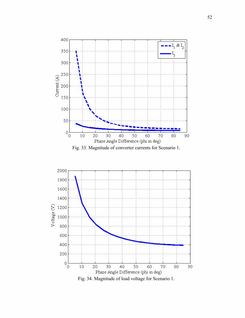
Fig. 34. Magnitude of load voltage for Scenario 1.
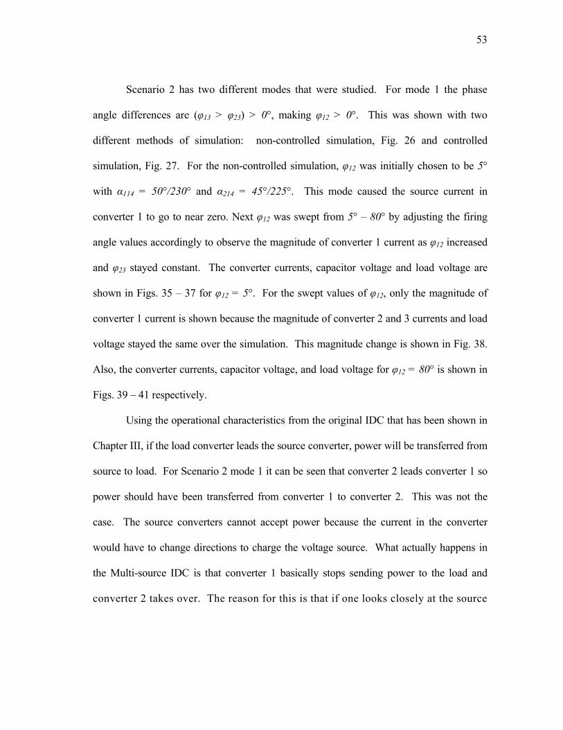
53
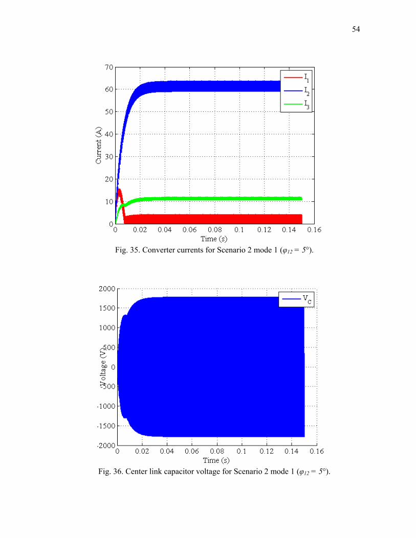
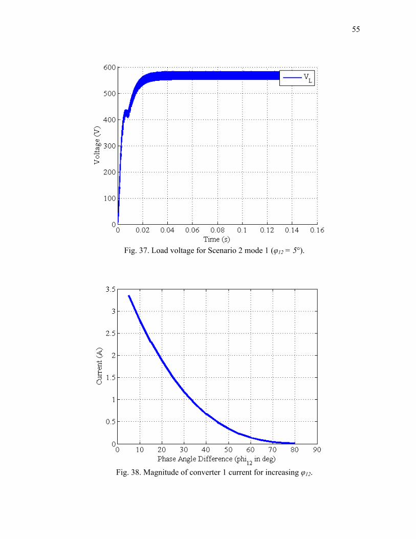
Scenario 2 has two different modes that were studied. For mode 1 the phase
angle differences are (φ13 > φ23) > 0°, making φ12 > 0°. This was shown with two
different methods of simulation: non-controlled simulation, Fig. 26 and controlled
simulation, Fig. 27. For the non-controlled simulation, φ12 was initially chosen to be 5°
with α114 = 50°/230° and α214 = 45°/225°. This mode caused the source current in
converter 1 to go to near zero. Next φ12 was swept from 5° – 80° by adjusting the firing
angle values accordingly to observe the magnitude of converter 1 current as φ12 increased
and φ23 stayed constant. The converter currents, capacitor voltage and load voltage are
shown in Figs. 35 – 37 for φ12 = 5°. For the swept values of φ12, only the magnitude of
converter 1 current is shown because the magnitude of converter 2 and 3 currents and load
voltage stayed the same over the simulation. This magnitude change is shown in Fig. 38.
Also, the converter currents, capacitor voltage, and load voltage for φ12 = 80° is shown in
Figs. 39 – 41 respectively.
Using the operational characteristics from the original IDC that has been shown in
Chapter III, if the load converter leads the source converter, power will be transferred from
source to load. For Scenario 2 mode 1 it can be seen that converter 2 leads converter 1 so
power should have been transferred from converter 1 to converter 2. This was not the
case. The source converters cannot accept power because the current in the converter
would have to change directions to charge the voltage source. What actually happens in
the Multi-source IDC is that converter 1 basically stops sending power to the load and
converter 2 takes over. The reason for this is that if one looks closely at the source
54
Fig. 35. Converter currents for Scenario 2 mode 1 (φ12 = 5°).
Fig. 36. Center link capacitor voltage for Scenario 2 mode 1 (φ12 = 5°).
55
Fig. 37. Load voltage for Scenario 2 mode 1 (φ12 = 5°).
Fig. 38. Magnitude of converter 1 current for increasing φ12.
56
Fig. 39. Converter currents for Scenario 2 mode 1 (φ12 = 80°).
Fig. 40. Center link capacitor voltage for Scenario 2 mode 1 (φ12 = 80°).
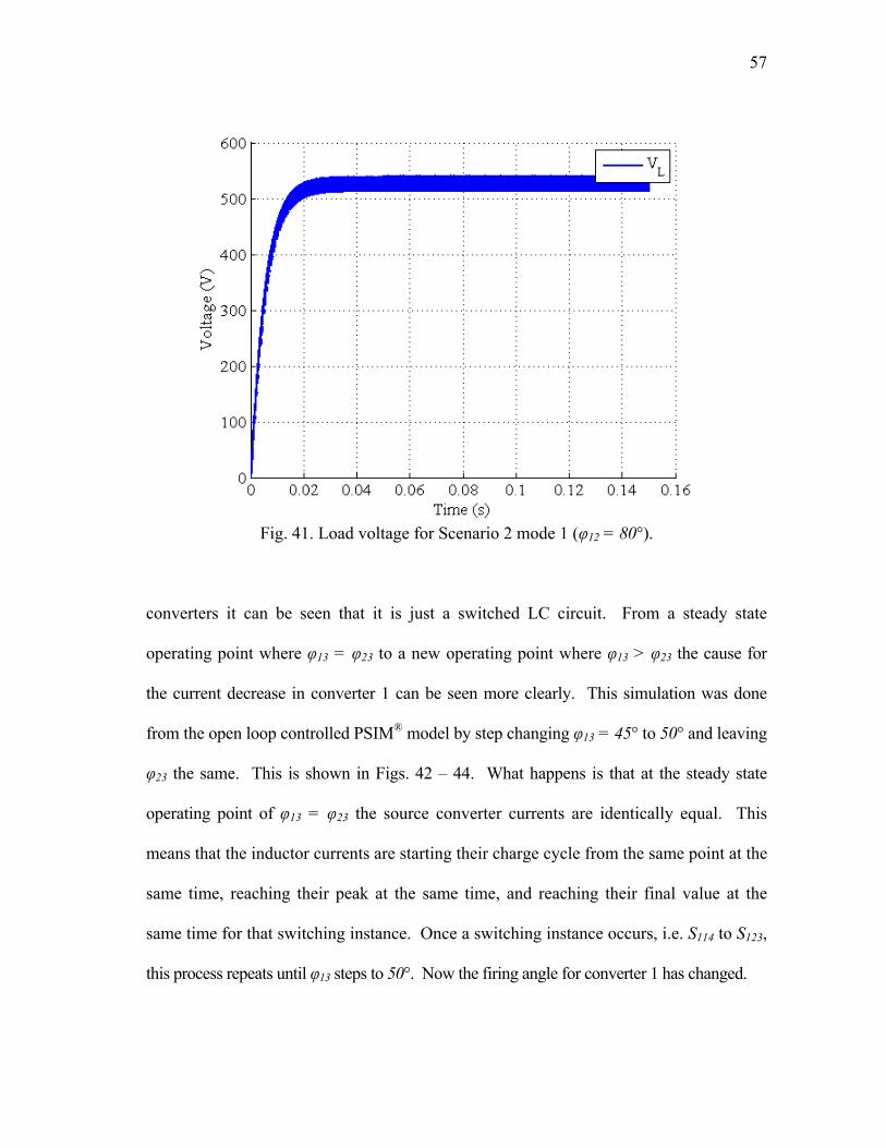
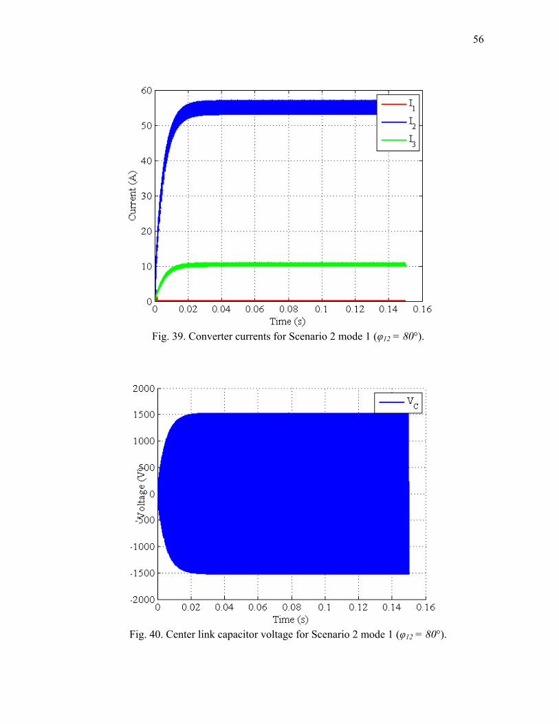
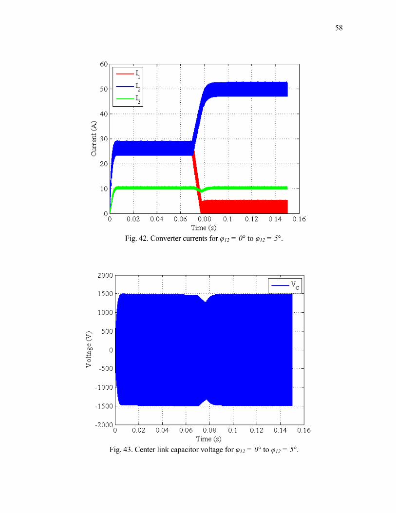
57
Fig. 41. Load voltage for Scenario 2 mode 1 (φ12 = 80°).
converters it can be seen that it is just a switched LC circuit. From a steady state
operating point where φ13 = φ23 to a new operating point where φ13 > φ23 the cause for
the current decrease in converter 1 can be seen more clearly. This simulation was done
from the open loop controlled PSIM® model by step changing φ13 = 45° to 50° and leaving
φ23 the same. This is shown in Figs. 42 – 44. What happens is that at the steady state
operating point of φ13 = φ23 the source converter currents are identically equal. This
means that the inductor currents are starting their charge cycle from the same point at the
same time, reaching their peak at the same time, and reaching their final value at the
same time for that switching instance. Once a switching instance occurs, i.e. S114 to S123,
this process repeats until φ13 steps to 50°. Now the firing angle for converter 1 has changed.
58
Fig. 42. Converter currents for φ12 = 0° to φ12 = 5°.
Fig. 43. Center link capacitor voltage for φ12 = 0° to φ12 = 5°.
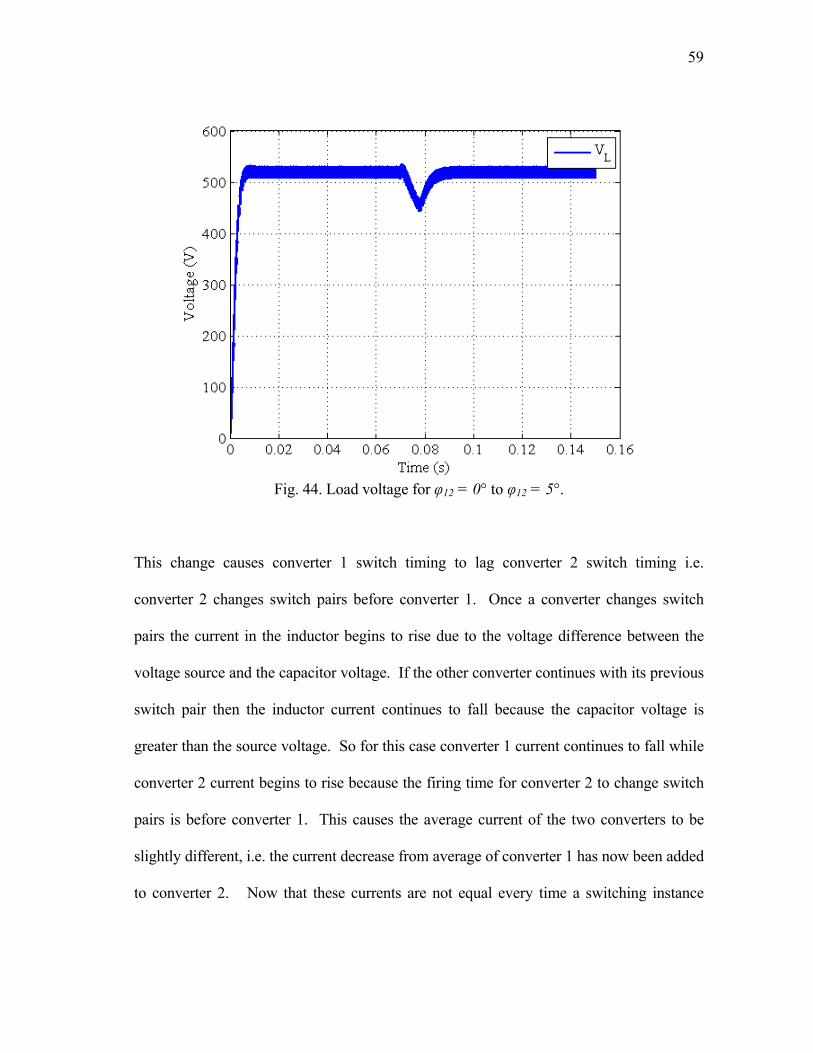
59
Fig. 44. Load voltage for φ12 = 0° to φ12 = 5°.
This change causes converter 1 switch timing to lag converter 2 switch timing i.e.
converter 2 changes switch pairs before converter 1. Once a converter changes switch
pairs the current in the inductor begins to rise due to the voltage difference between the
voltage source and the capacitor voltage. If the other converter continues with its previous
switch pair then the inductor current continues to fall because the capacitor voltage is
greater than the source voltage. So for this case converter 1 current continues to fall while
converter 2 current begins to rise because the firing time for converter 2 to change switch
pairs is before converter 1. This causes the average current of the two converters to be
slightly different, i.e. the current decrease from average of converter 1 has now been added
to converter 2. Now that these currents are not equal every time a switching instance
60
occurs the currents will not cancel each other out while charging the center capacitor,
converter 2 will dominate the charging. Now the time for converter 1 inductor current to
reach its peak value is slightly shorter than the time it takes to fall back to its original
starting point for that switching instance. This causes the current in converter 1 to
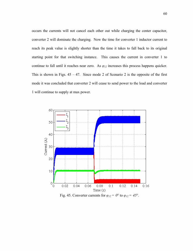
continue to fall until it reaches near zero. As φ12 increases this process happens quicker.
This is shown in Figs. 45 – 47. Since mode 2 of Scenario 2 is the opposite of the first
mode it was concluded that converter 2 will cease to send power to the load and converter
1 will continue to supply at max power.
Fig. 45. Converter currents for φ12 = 0° to φ12 = 45°.
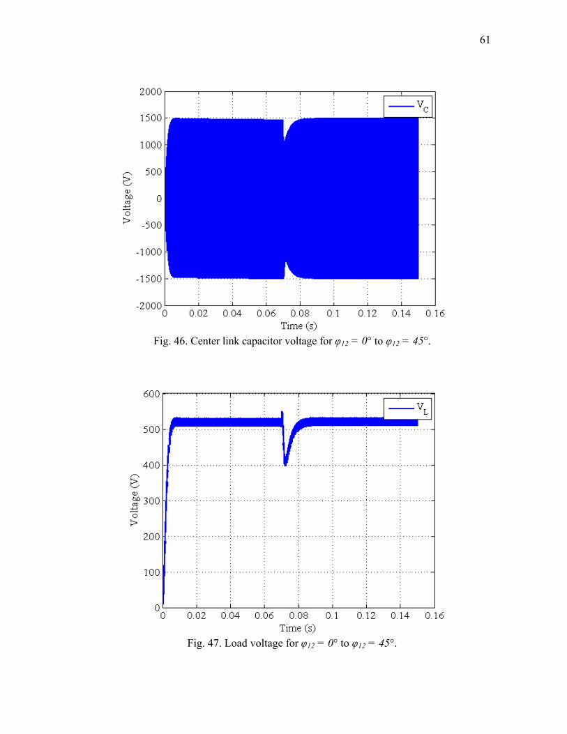
61
Fig. 46. Center link capacitor voltage for φ12 = 0° to φ12 = 45°.
Fig. 47. Load voltage for φ12 = 0° to φ12 = 45°.
62
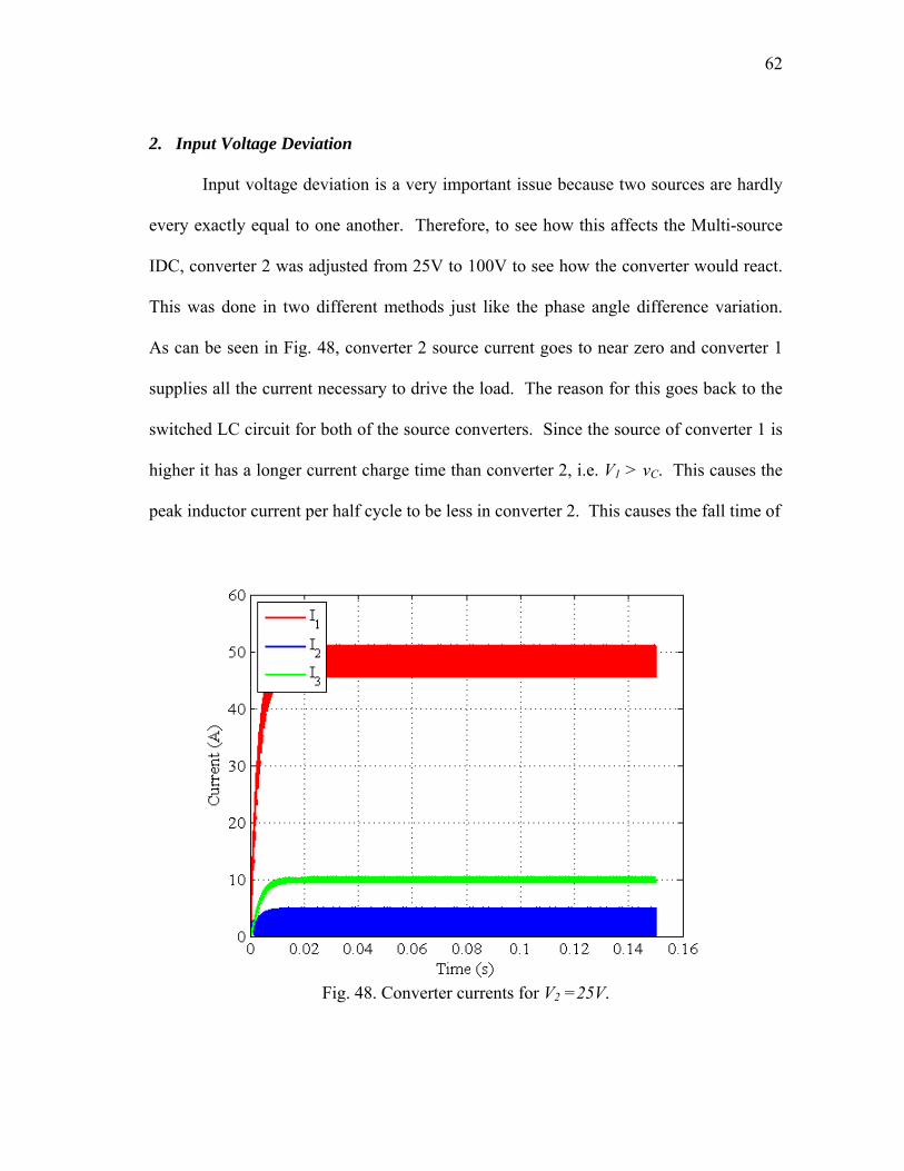
2. Input Voltage Deviation
Input voltage deviation is a very important issue because two sources are hardly
every exactly equal to one another. Therefore, to see how this affects the Multi-source
IDC, converter 2 was adjusted from 25V to 100V to see how the converter would react.
This was done in two different methods just like the phase angle difference variation.
As can be seen in Fig. 48, converter 2 source current goes to near zero and converter 1
supplies all the current necessary to drive the load. The reason for this goes back to the
switched LC circuit for both of the source converters. Since the source of converter 1 is
higher it has a longer current charge time than converter 2, i.e. V1 > vC. This causes the
peak inductor current per half cycle to be less in converter 2. This causes the fall time of
Fig. 48. Converter currents for V2 =25V.
63
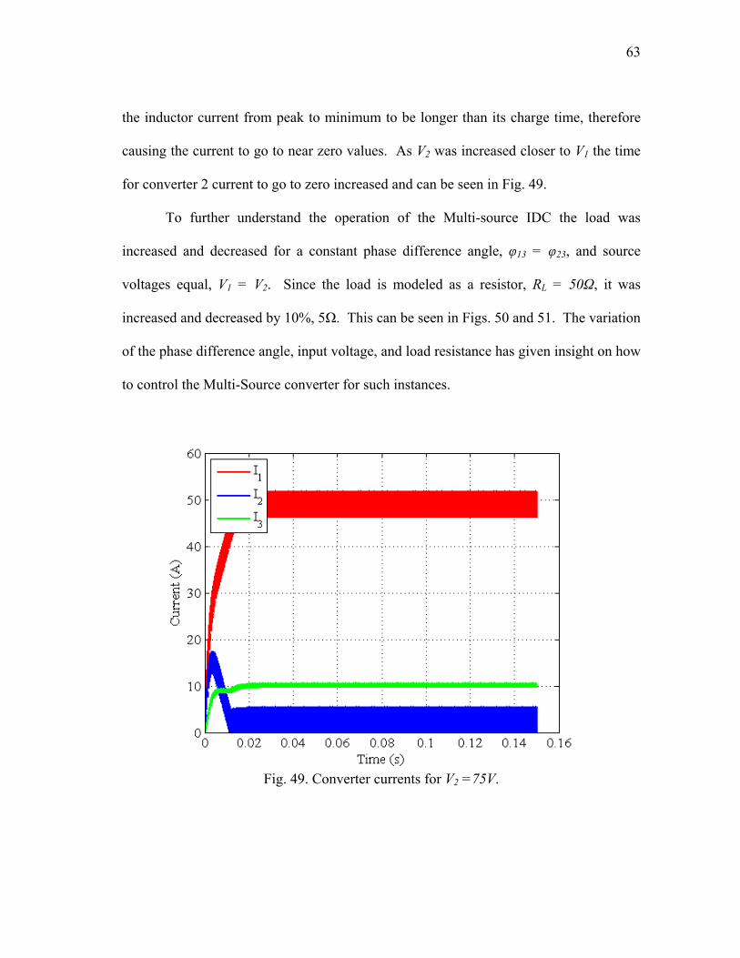
the inductor current from peak to minimum to be longer than its charge time, therefore
causing the current to go to near zero values. As V2 was increased closer to V1 the time
for converter 2 current to go to zero increased and can be seen in Fig. 49.
To further understand the operation of the Multi-source IDC the load was
increased and decreased for a constant phase difference angle, φ13 = φ23, and source
voltages equal, V1 = V2. Since the load is modeled as a resistor, RL = 50Ω, it was
increased and decreased by 10%, 5Ω. This can be seen in Figs. 50 and 51. The variation
of the phase difference angle, input voltage, and load resistance has given insight on how
to control the Multi-Source converter for such instances.
Fig. 49. Converter currents for V2 =75V.
64
Fig. 50. Load voltage for RL = 50Ω to 45 Ω.
Fig. 51. Load voltage for RL = 50Ω to 55Ω.

65
B. Control Results
By observing how the phase difference angle, input voltage, and load resistance
changed the operational characteristics of the Multi-source IDC, a simple yet elegant
way to regulate the output voltage and converter 2 input current was obtained and shown
in Chapter III. Various control schemes were simulated in order to show that this
control method was valid for different variations in load, input current, and input
voltage. Each of these simulations have three parts: steady state, 1st variation, and 2nd
variation. All simulations were simulated for 0.2s. The control algorithm takes the
average value of the measurement in order to determine if converter 2 current or load
voltage is within its hysteresis band. These average values are shown along with the
actual measured value for that specific element.
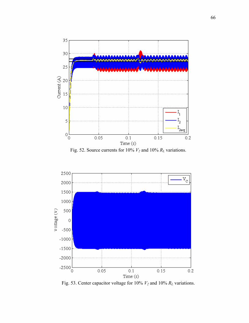
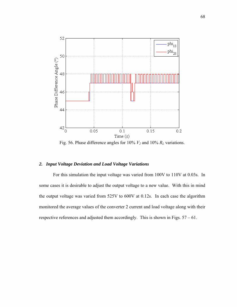
1. Input Voltage Deviation and Load Variation
For this simulation the first variation comes at 0.04s with the converter 2 voltage,
V2, changing from 100V to 110V. Once this deviation occurs the controller responds to
converter 2 current going out of bounds, greater or less than 27.5 plus hysteresis, and
adjusts φ23 accordingly. Shortly thereafter, the output voltage goes out of its hysteresis
band and φ13 is adjusted and φ23 is set equal to φ13 until the current goes out of its band
again. At 0.12s the load resistance is changed from 50 to 45, which causes a voltage
spike. The control algorithm then adjusts φ13 in order to keep the output voltage
regulated and then tends to φ23 to monitor the input current of converter 2. This is
shown in Fig. 52 – 56. The load was also varied by 20% and is shown in Appendix C.
66
Fig. 52. Source currents for 10% V2 and 10% RL variations.
Fig. 53. Center capacitor voltage for 10% V2 and 10% RL variations.
67
Fig. 54. Load current for 10% V2 and 10% RL variations.
Fig. 55. Load voltage for 10% V2 and 10% RL variations.
68
Fig. 56. Phase difference angles for 10% V2 and 10% RL variations.
2. Input Voltage Deviation and Load Voltage Variations
For this simulation the input voltage was varied from 100V to 110V at 0.03s. In
some cases it is desirable to adjust the output voltage to a new value. With this in mind
the output voltage was varied from 525V to 600V at 0.12s. In each case the algorithm
monitored the average values of the converter 2 current and load voltage along with their
respective references and adjusted them accordingly. This is shown in Figs. 57 – 61.
69
Fig. 57. Source currents for 10% V2 and 10% VL variations.
Fig. 58. Center capacitor voltage for 10% V2 and 10% VL variations.
70
Fig. 59. Load current for 10% V2 and 10% VL variations.
Fig. 60. Load voltage for 10% V2 and 10% VL variations.
71
Fig. 61. Phase difference angles for 10% V2 and 10% VL variations.
3. Input Voltage Deviation and Input Current Variations
For this simulation the input voltage was varied from 100V to 110V at 0.03s.
After this three different variations of current control were simulated. This is to show
the flexibility of the control to monitor the source that is considered to be the short term
source and turn it off through a ramp down sequence or to increase or decrease the
current from this source based on its capacity. For the first simulation the input current
was stepped down to 20A. The second simulation was a ramp down to near 0A. The
third simulation was to ramp down to 0A and then ramp up to 27.5A to show that the
source can be turned back on when necessary. This is shown in Figs. 62 – 70. The
capacitor voltage and load current are shown in Appendix D.
72
Fig. 62. Source currents for 10% V2 and 25% I2 variations.
Fig. 63. Load voltage for 10% V2 and 25% I2 variations.
73
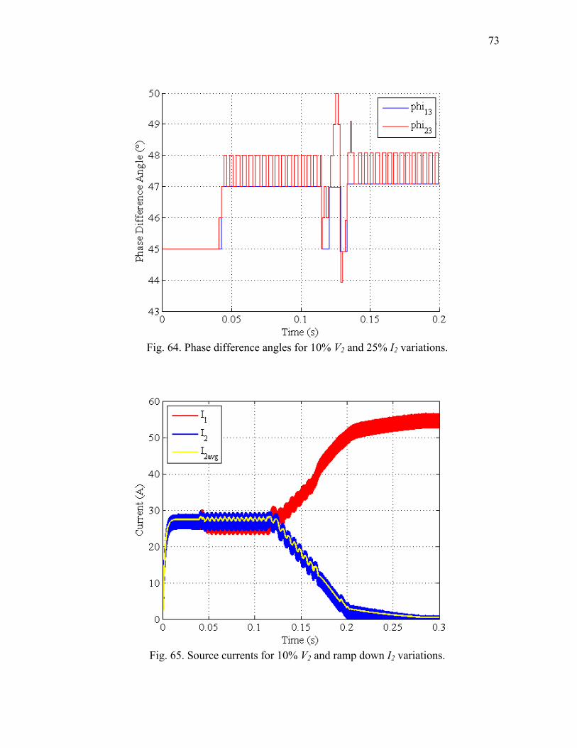
Fig. 64. Phase difference angles for 10% V2 and 25% I2 variations.
Fig. 65. Source currents for 10% V2 and ramp down I2 variations.
74
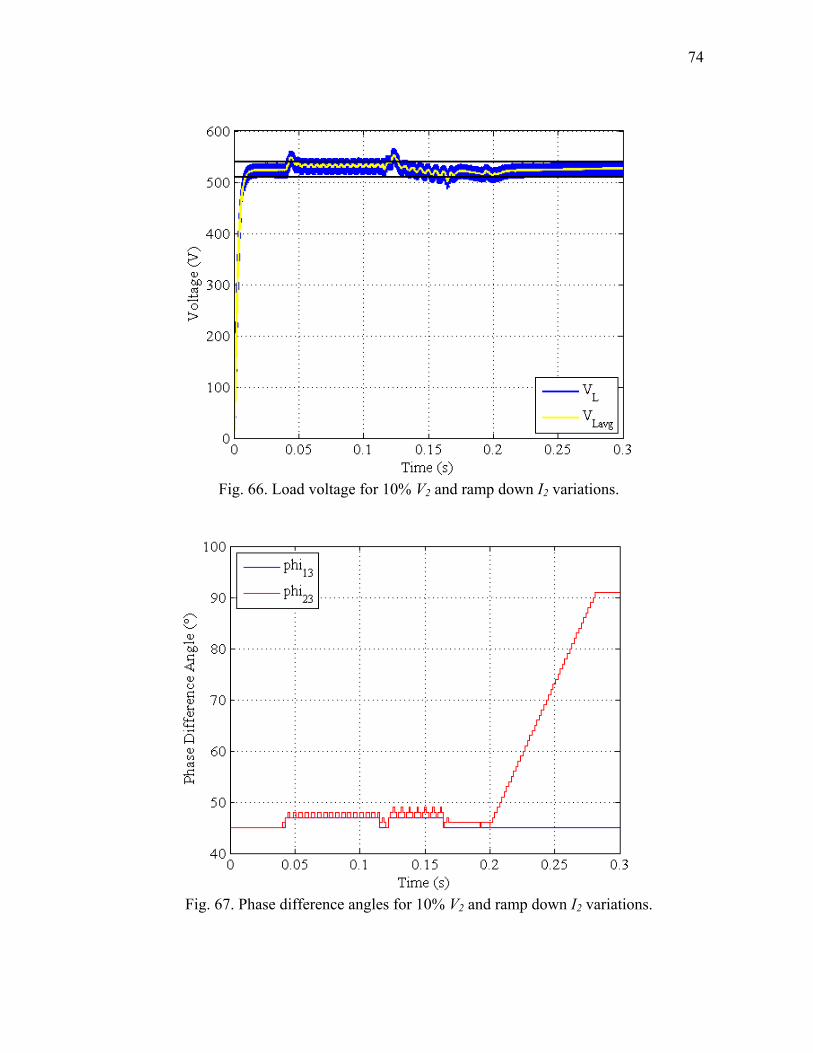
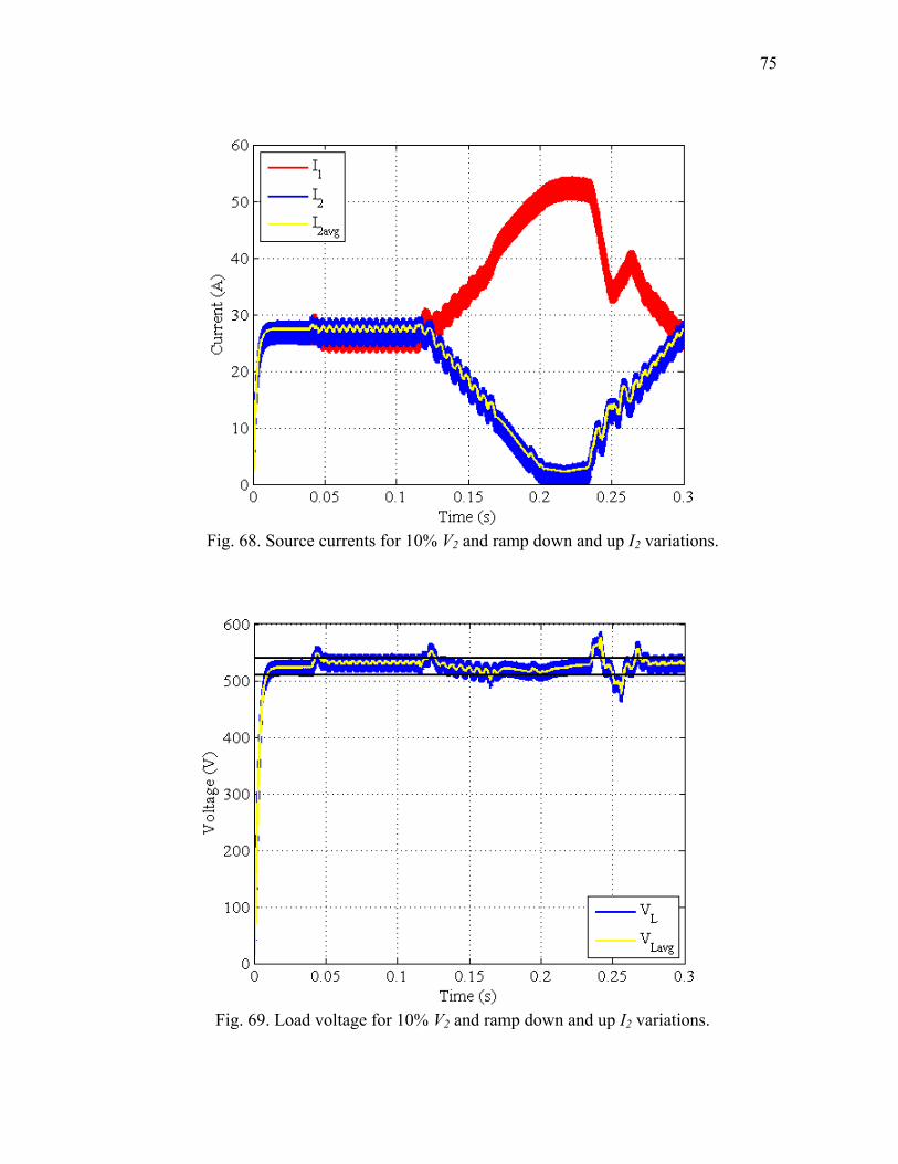
Fig. 66. Load voltage for 10% V2 and ramp down I2 variations.
Fig. 67. Phase difference angles for 10% V2 and ramp down I2 variations.
75
Fig. 68. Source currents for 10% V2 and ramp down and up I2 variations.
Fig. 69. Load voltage for 10% V2 and ramp down and up I2 variations.
76
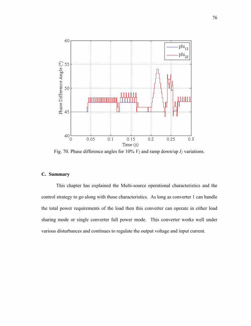
Fig. 70. Phase difference angles for 10% V2 and ramp down/up I2 variations.
C. Summary
This chapter has explained the Multi-source operational characteristics and the
control strategy to go along with those characteristics. As long as converter 1 can handle
the total power requirements of the load then this converter can operate in either load
sharing mode or single converter full power mode. This converter works well under
various disturbances and continues to regulate the output voltage and input current.
77
CHAPTER V
CONCLUSIONS AND FUTURE WORK
A. Conclusions
With the need for renewable energy sources in high demand, the technology
needed to interface these sources has been a big topic in current research with the
creation of new conferences and transactions. This thesis has presented a new DC-DC
converter, Multi-source IDC, which can be used with multiple energy sources.
The Multi-source IDC is a topological variation of the original IDC presented in
Chapter II. The original IDC is a DC-DC converter with the capability of continuous
voltage step up or step down over a wide range without the use of a transformer. This is
done by controlling the phase difference angle φ or the switching frequency f. This
converter was then modeled using Gyrator theory in order to gain an understanding
about its operational characteristics as well as control.
A new DC-DC converter was presented in Chapter III based on the original IDC.
This converter, Multi-source IDC, is a topological variation of the IDC. This converter
consists of two source converters attached to a center link capacitor and then connected
to the load converter. This new converter was then studied based on various
disturbances that may occur while operating a multiple source system as well as the
responses to similar control techniques from the original IDC.
First this study showed that when the phase difference angles are equal, i.e. φ13 =
φ23, the Multi-source IDC operates the same as the original IDC with the exception that
78
the original source current in the IDC is now split between the two converters in the
Multi-source IDC. Therefore, this new converter is doing equal load sharing. From this
observation it was then desired to operate the converters at different power levels by
adjusting their current. This was done by actively controlling the phase difference angle
φ23 in such a way that converter 2 current stayed within the bounds of the desired
reference current. It was also desired to control the output voltage across the load during
times of disturbance or transients from one power level to the next. This was done by
adjusting φ13 in such a way to keep the output voltage regulated within a tolerable
hysteresis band. Both of these controls, input current and output voltage, were then
implemented into one controller in order to maintain the input current of converter 2
within a particular set of values as well as hold the output voltage within its set of
values. By doing this the Multi-source converter demonstrated that it can be controlled
in such a fashion to supply a single load from one limitless supply and one varying
supply.
B. Future Work
This project will be extended by placing this converter topology and its control
into a particular application. This application will be stand alone power generation via a
fuel cell and battery power supply. This study will include but is not limited to:
electrical fuel cell modeling in PSIM®, battery modeling in PSIM®, battery recharging,
and balance of plant control based on energy capacity.
79
REFERENCES
[1] H. Tao, A. Kotsopoulos, J.L. Duarte, and M.A.M. Hendrix, “Family of multiport bidirectional DC–DC converters,” IEE Proceedings of Electric Power Applications, vol. 153, no. 3, pp. 451-458, May 2006.
[2] J.L. Duarte, M. Hendrix, and M.G. Simoes, “Three-port bidirectional converter for hybrid fuel cell systems,” IEEE Transactions on Power Electronics, vol. 22, no. 2, pp. 480-487, March 2007.
[3] Y.M. Chen, Y.C. Liu, S.C. Hung, and C.S. Cheng, “Multi-input inverter for grid-connected hybrid PV/wind power system,” IEEE Transactions on Power Electronics, vol. 22, no. 3, pp. 1070-1077, May 2007.
[4] C. Zao, S. Round, and J.W. Kolar, “Buck and boost start-up operation of a three-port power supply for hybrid vehicle applications,” in Proc. 36th Annual Power Electronics Specialists Conference, 2005, pp. 1851-1857.
[5] J.G. Kassakian, H.C. Wolf, J.M. Miller, and C.J. Hurton, “Automotive electrical systems circa 2005,” IEEE Spectrum, vol. 33, no. 8, pp. 22-27, Aug. 1996.
[6] H. Krishnaswami and N. Mohan, “A Current-fed three-port bi-directional DC-DC converter,” in Proc. 29th International Telecommunications Energy Conference, Sept. 30, 2007-Oct. 4, 2007, pp. 523-526.
[7] H. Tao, A. Kotsopoulos, J.L. Duarte, and M.A.M. Hendrix, “Multi-input bidirectional DC-DC converter combining DC-link and magnetic-coupling for fuel cell systems,” in Proc. 40th Annual Meeting Industry Applications Conference, vol. 3, Oct. 2-6, 2005, pp. 2021-2028.
[8] Y.M. Chen, Y.C. Liu, and F.Y. Wu, “Multi-input DC/DC converter based on the multiwinding transformer for renewable energy applications,” IEEE Transactions on Industry Applications, vol. 38, no. 4, pp. 1096-1104, July-Aug. 2002.
[9] H. Tao, A. Kotsopoulos, J.L. Duarte, and M.A.M. Hendrix, “A soft-switched three-port bidirectional converter for fuel cell and supercapacitor applications,” in Proc. 36th Annual Power Electronics Specialists Conference, 2005, pp. 2487-2493.

80
[10] R.W. De Donker, D.M. Divan, and M.H. Kheraluwala, “A three-phase soft-switched high-power-density DC/DC converter for high-power applications,” IEEE Transactions on Industry Applications, vol. 27, no. 1, pp. 63-73, Jan.-Feb. 1991.
[11] M. Ehsani, R.L. Kustom, and R.W. Boom, “A one-phase dual converter for two quadrant power control of superconducting magnets,” IEEE Transactions on Magnetics, vol. 21, no. 2, pp. 1115-1118, Mar. 1985.
[12] M. Ehsani and R.L. Kustom, Converter Circuits for Superconductive Magnetic Energy Storage, Texas A&M University Press, College Station, Texas, 1988.
[13] M.O. Bilgiç and M. Ehsani, “Analysis of inductor-converter bridge by means of state-space averaging technique,” in Proc. 19th Annual Power Electronics Specialists Conference, 1988, pp. 116-121.
[14] I. Husain, Analysis and Design of a High Power DC-DC Converter, M.S. Thesis, Texas A&M University, College Station, 1989.
[15] S. Singer, “Gyrators in power processing circuits,” IEEE Transactions on Industrial Electronics, vol. 34, no. 3, pp. 313-318, Aug. 1987.
[16] M. Ehsani, “Inverse dual converter for high-power applications,” U.S. Patent, Patent # 5,208,740, May 4, 1993.
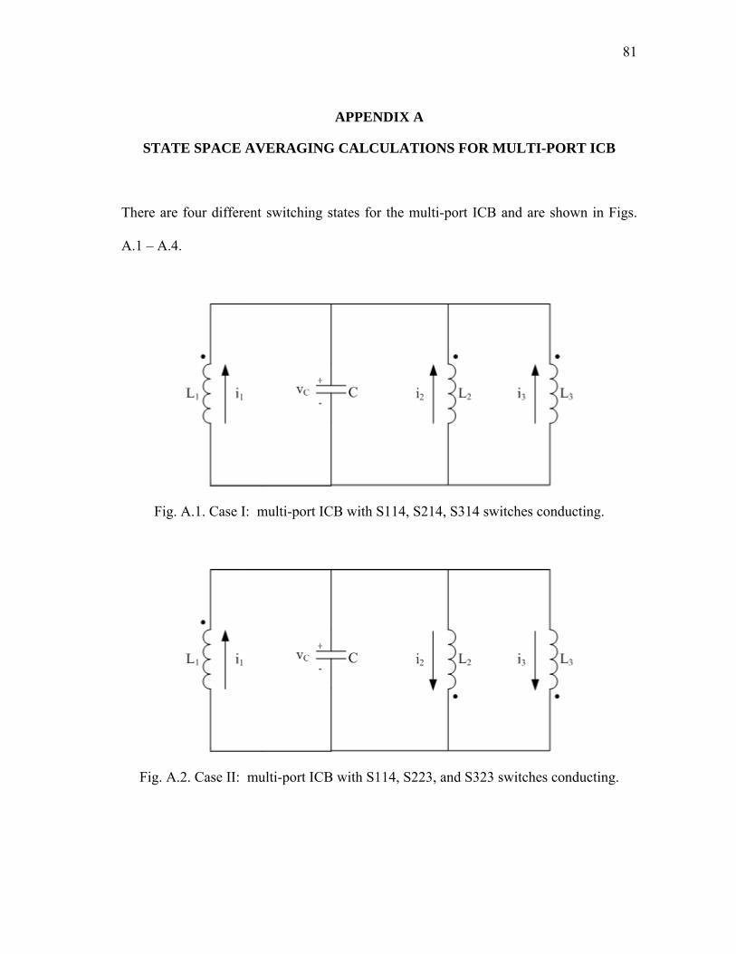
81
APPENDIX A
STATE SPACE AVERAGING CALCULATIONS FOR MULTI-PORT ICB
There are four different switching states for the multi-port ICB and are shown in Figs.
A.1 – A.4.
Fig. A.1. Case I: multi-port ICB with S114, S214, S314 switches conducting.
Fig. A.2. Case II: multi-port ICB with S114, S223, and S323 switches conducting.
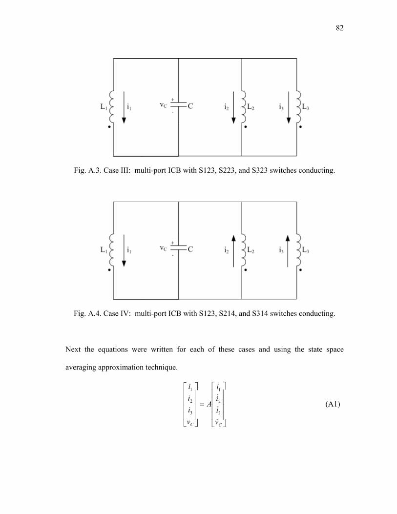
82
Fig. A.3. Case III: multi-port ICB with S123, S223, and S323 switches conducting.
Fig. A.4. Case IV: multi-port ICB with S123, S214, and S314 switches conducting.
Next the equations were written for each of these cases and using the state space
averaging approximation technique.
CC v
i
i
i
A
v
i
i
i
3
2
1
3
2
1
(A1)
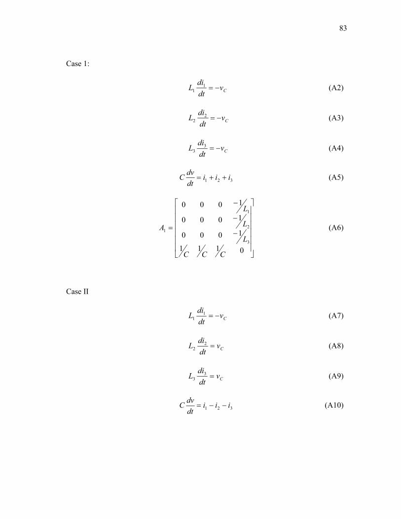
83
Case 1:
Cvdt
diL 1
1 (A2)
Cvdt
diL 2
2 (A3)
Cvdt
diL 3
3 (A4)
321 iiidt
dvC (A5)
0111
1000
1000
1000
3
2
1
1
CCC
L
L
L
A (A6)
Case II
Cvdt
diL 1
1 (A7)
Cvdt
diL 2
2 (A8)
Cvdt
diL 3
3 (A9)
321 iiidt
dvC (A10)
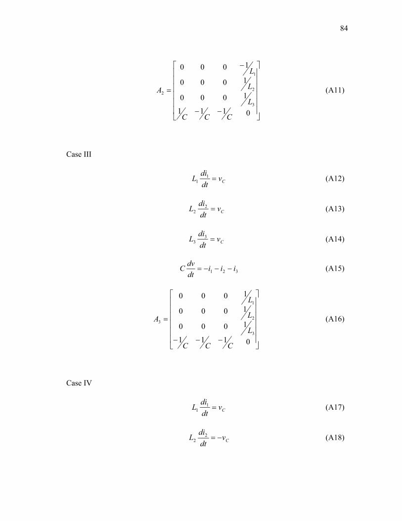
84
0111
1000
1000
1000
3
2
1
2
CCC
L
L
L
A (A11)
Case III
Cvdt
diL 1
1 (A12)
Cvdt
diL 2
2 (A13)
Cvdt
diL 3
3 (A14)
321 iiidt
dvC (A15)
0111
1000
1000
1000
3
2
1
3
CCC
L
L
L
A (A16)
Case IV
Cvdt
diL 1
1 (A17)
Cvdt
diL 2
2 (A18)

85
Cvdt
diL 3
3 (A19)
321 iiidt
dvC (A20)
0111
1000
1000
1000
3
2
1
4
CCC
L
L
L
A (A21)
Next using the following approximation to estimate the four different state matrices the
final equations can be written.
TddAAAAA 1221 (A22)
where,
2
d (A23)
T
2 (A24)
2
5.0 d (A25)
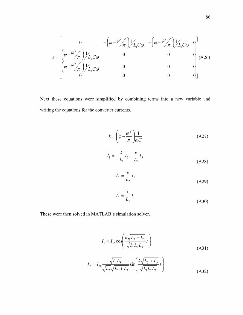
86
0000
0001
0001
0110
3
2
2
2
1
2
1
2
CL
CL
CLCL
A (A26)
Next these equations were simplified by combining terms into a new variable and
writing the equations for the converter currents.
C
k
12
(A27)
3
12
11 I
L
kI
L
kI
(A28)
1
22 I
L
kI
(A29)
1
33 I
L
kI
(A30)
These were then solved in MATLAB’s simulation solver.
t
LLL
LLkII O
321
321 cos
(A31)
t
LLL
LLk
LLL
LLII O
321
32
322
312 sin
(A32)

87
t
LLL
LLk
LLL
LLII O
321
32
323
213 sin
(A33)

88
APPENDIX B
SOURCE CODE FOR FEEDBACK CONTROL OF MULTI-SOURCE IDC
// Feedback Control of Multi-Source IDC // Written by: Billy Yancey // Defining variables static double phi13 = 45, phi13_o = 45, phi13_c = 45, phi23_o = 45, phi23_c = 45; static double pi = 3.1416, theta = 0, m = 0, a = 0, b = 0, V2o = 100, k = 0, n = 0, del_phi_o = 1, del_phi = 1, c = 0, d = 0, mc1 = 0, mc2 = 0, I2_o = 0; double Vo, Voref, Vrip, S114, S123, S214, S223, S314, S323, f, phi23, V2, I2, I2ref, phi223, phi13_r, E, h, g, gnew, grat, w; // Initializing switching frequency f = 5000; // Defining inputs Vo = x1; V2 = x2; I2 = x3; Voref = x4; I2ref = x5; // Defining variables Vrip = 15; //ripple voltage w = 2*pi*f; //angular frequency // Creating a repeating theta from 0 - 360 if (theta >= 360) theta = 0; m++; else theta = 2*180*f*t - 2*180*m; // Control of Converter 3 if (theta >= 0 && theta <= 180) S314 = 1;

89
S323 = 0; else S314 = 0; S323 = 1; // Voltage control algorithm if (t >= 0.025 && a == 0) if(((Vo > Voref+Vrip) || (Vo < Voref-Vrip)) && m >= mc1+25) phi13_r = phi13_o*pi/180; g = w*2e-6/(phi13_r-pow(phi13_r,2)/pi); grat = Voref/Vo; gnew = grat*g; E = sqrt(gnew*gnew*pi*pi-4*gnew*w*2e-6*pi); //phi_c = 1/2/gnew*(gnew*3.1416-E)*180/3.1416; phi13_c = 1/(2*gnew)*(gnew*pi-E)*(180/pi); phi23_c = phi13_c; //phi_c = grat*phi_r*180/pi; h = 0; mc1 = m; else phi13 = phi13_o; h = 1; else phi13 = phi13_c; h = 3; if (phi13_c == phi13_o) phi13_o = phi13; else if (theta <= 5)

90
a = 1;
else phi13_o = phi13; // Checking for change in input voltage if (t <= 0.025 && ((I2 > I2ref+0.5) || (I2 < I2ref+0.5))) //if ((((V2o+0.00001) >= V2 && (V2o-0.00001) <= V2)) || (t >= 0.01 && ((I2 > I2ref+0.5) || (I2 < I2ref+0.5)))) k = 0; else k = 1; // Current regulation for converter 2 algorithm if (k == 1 && b == 0) if ((I2 > I2ref+0.5) && c == 0) phi23_c = phi23_o + del_phi_o; phi23 = phi23_c; del_phi = del_phi_o; c = 1; d = 0; mc2 = m; I2_o = I2; else if ((I2 < I2ref-0.5) && d == 0) phi23_c = phi23_o - del_phi_o; phi23 = phi23_c; del_phi = del_phi_o; c = 0; d = 1;
91
mc2 = m; I2_o = I2; //del_phi_o = del_phi; else if ((I2 < I2ref-0.5) && (m > mc2+8)) c = 1; d = 0; phi23 = phi23_c; del_phi = del_phi_o; else if ((I2 > I2ref+0.5) && (m > mc2+8)) c = 0; d = 1; phi23 = phi23_c; del_phi = del_phi_o; else phi23 = phi23_c; del_phi = del_phi_o; del_phi_o = del_phi; else phi23 = phi23_c; del_phi_o = del_phi; // Checking for duty cycle change of Converter 2 if (phi23 == phi23_o) phi23_o = phi23; else if (theta <= 0.05)
92
b = 1; else // Firing angle control for Converter 1 if (a == 0) if (theta >= phi13_o && theta <= (180+phi13_o)) S114 = 1; S123 = 0; else if (theta >= (180+phi13_o) && theta <= 360) S114 = 0; S123 = 1; else S114 = 0; S123 = 1; // Phase shift control for Converter 1 else if (a == 1) if (theta >= (phi13_o+((phi13-phi13_o)/2)) && theta <= (180+(phi13_o+((phi13-phi13_o)/2)))) S114 = 1; S123 = 0; else if (theta >= (180+(phi13_o+((phi13-phi13_o)/2))) && theta <= 360) S114 = 0; S123 = 1; else

93
S114 = 0; S123 = 1; // Checking to end phase shifting technique if (theta >= 180) a = 0; phi13_o = phi13; else a = 1; // Firing angle control for Converter 2 if (b == 0) if (theta >= phi23_o && theta <= (180+phi23_o)) S214 = 1; S223 = 0; else if (theta >= (180+phi23_o) && theta <= 360) S214 = 0; S223 = 1; else S214 = 0; S223 = 1; // Phase shift control for Converter 2 else if (b == 1) if (theta >= (phi23_o+((phi23-phi23_o)/2)) && theta <= (180+(phi23_o+((phi23-phi23_o)/2)))) S214 = 1;

94
S223 = 0; else if (theta >= (180+(phi23_o+((phi23-phi23_o)/2))) && theta <= 360) S214 = 0; S223 = 1; else S214 = 0; S223 = 1; // Checking to end phase shifting technique if (theta >= 180) b = 0; phi23_o = phi23; else b = 1; // Defining outputs y1 = S114; y2 = S123; y3 = S214; y4 = S223; y5 = S314; y6 = S323; y7 = phi13; y8 = phi23;
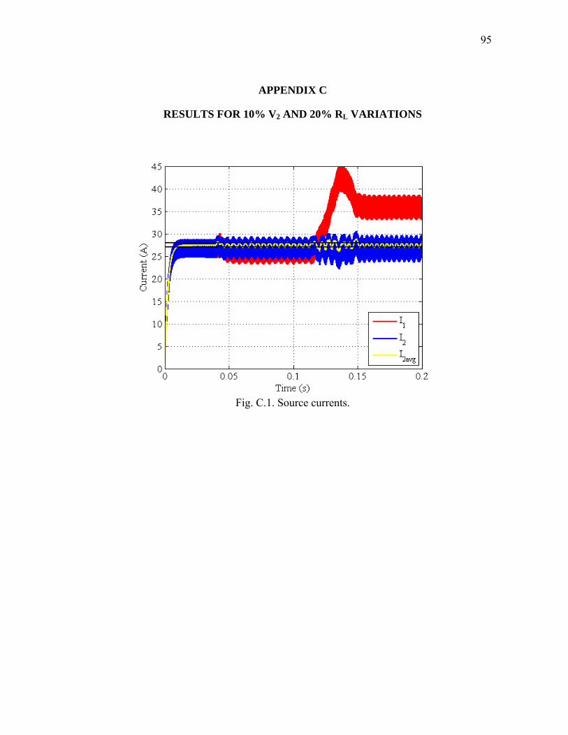
95
APPENDIX C
RESULTS FOR 10% V2 AND 20% RL VARIATIONS
Fig. C.1. Source currents.
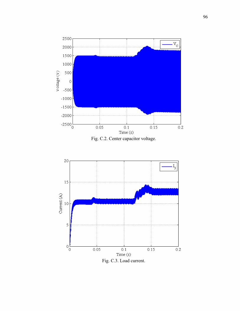
96
Fig. C.2. Center capacitor voltage.
Fig. C.3. Load current.

97
Fig. C.4. Load voltage.
Fig. C.5. Phase difference angles.
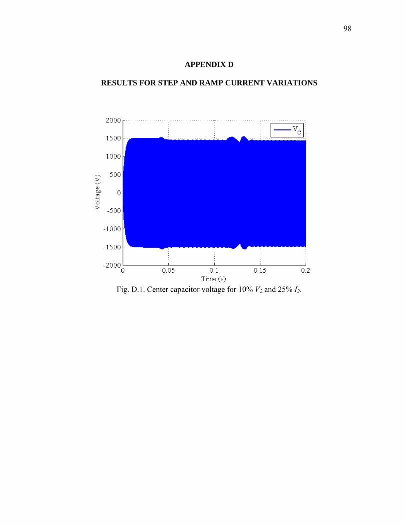
98
APPENDIX D
RESULTS FOR STEP AND RAMP CURRENT VARIATIONS
Fig. D.1. Center capacitor voltage for 10% V2 and 25% I2.
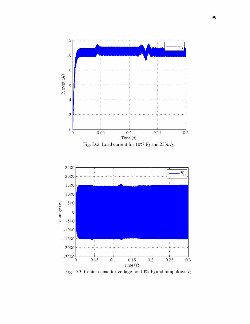
99
Fig. D.2. Load current for 10% V2 and 25% I2.
Fig. D.3. Center capacitor voltage for 10% V2 and ramp down I2.

100
Fig. D.4. Load current for 10% V2 and ramp down I2.
Fig. D.5. Center capacitor voltage for 10% V2 and ramp down/up I2.
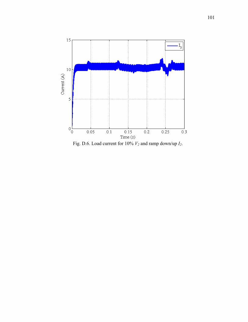
101
Fig. D.6. Load current for 10% V2 and ramp down/up I2.
102
VITA
Billy Ferrall Yancey III received his Bachelor of Science in engineering from
Arkansas State University in December of 2005. Upon graduation he entered into the
graduate program in the Department of Electrical Engineering at University of Missouri-
Rolla where he specialized in electromagnetics. After one semester he then transferred
to the graduate program in the Department of Computer and Electrical Engineering at
Texas A&M University where he specialized in power electronics and motor drives. He
received his Master of Science in electrical engineering in May of 2010. His research
interests include sustainable energy, power electronic converters for energy storage, and
design and control of electrical machines.
He can be reached at [email protected] or through his advisor Dr. M.
Ehsani, Professor, Department of Electrical and Computer Engineering, 3128 TAMU,
Texas A&M University, College Station, TX 77843.