Embed Size (px)
Citation preview

University of Central Florida University of Central Florida
STARS STARS
Electronic Theses and Dissertations, 2004-2019
2010
Modeling And Design Of Multi-port Dc/dc Converters Modeling And Design Of Multi-port Dc/dc Converters
Zhijun Qian University of Central Florida
Part of the Electrical and Electronics Commons
Find similar works at: https://stars.library.ucf.edu/etd
University of Central Florida Libraries http://library.ucf.edu
This Doctoral Dissertation (Open Access) is brought to you for free and open access by STARS. It has been accepted
for inclusion in Electronic Theses and Dissertations, 2004-2019 by an authorized administrator of STARS. For more
information, please contact [email protected].
STARS Citation STARS Citation Qian, Zhijun, "Modeling And Design Of Multi-port Dc/dc Converters" (2010). Electronic Theses and Dissertations, 2004-2019. 1543. https://stars.library.ucf.edu/etd/1543
MODELING AND DESIGN OF MULTI-PORT DC/DC CONVERTERS
by
ZHIJUN QIAN B.S. Zhejiang University, 2005 M.S. Zhejiang University, 2007
A dissertation submitted in partial fulfillment of the requirements for the degree of Doctor of Philosophy
in the Department of Electrical Engineering and Computer Science in the College of Engineering and Computer Science
at the University of Central Florida Orlando, Florida
Spring Term 2010
Major Professor: Issa Batarseh

ii
© 2010 ZHIJUN QIAN

iii
To my wife

iv
ABSTRACT
In this dissertation, a new satellite platform power architecture based on paralleled three-port
DC/DC converters is proposed to reduce the total satellite power system mass. Moreover, a four-
port DC/DC converter is proposed for renewable energy applications where several renewable
sources are employed. Compared to the traditional two-port converter, three-port or four-port
converters are classified as multi-port converters. Multi-port converters have less component
count and less conversion stage than the traditional power processing solution which adopts
several independent two-port converters. Due to their advantages multi-port converters recently
have attracted much attention in academia, resulting in many topologies for various applications.
But all proposed topologies have at least one of the following disadvantages: 1) no bidirectional
port; 2) lack of proper isolation; 3) too many active and passive components; 4) no soft-
switching. In addition, most existing research focuses on the topology investigation, but lacks
study on the multi-port converter’s control aspects, which are actually very challenging since it is
a multi-input multi-output control system and has so many cross-coupled control loops.
A three-port converter is proposed and used for space applications. The topology features
bidirectional capability, low component count and soft-switching for all active switches, and has
one output port to meet certain isolating requirements. For the system level control strategy, the
multi-functional central controller has to achieve maximal power harvesting for the solar panel,
the battery charge control for the battery, and output voltage regulation for the dc bus. In order to
design these various controllers, a good dynamic model of the control object should be obtained
first. Therefore, a modeling procedure based on a traditional state-space averaging method is

v
proposed to characterize the dynamic behavior of such a multi-port converter. The proposed
modeling method is clear and easy to follow, and can be extended for other multi-port converters.
In order to boost the power level of the multi-port converter system and allow redundancy, the
three-port converters are paralleled together. The current sharing control for the multi-port
converters has rarely been reported. A so called “dual loop” current sharing control structure is
identified to be suitable for the paralleled multi-port converters, since its current loop and the
voltage loop can be considered and designed independently, which simplifies the multi-port
converter’s loop analysis. The design criteria for that dual loop structure are also studied to
achieve good current sharing dynamics while guaranteeing the system stability.
The renewable energy applications are continuously demanding the low cost solution, so that the
renewable energy might have a more competitive dollar per kilowatt figure than the traditional
fossil fuel power generation. For this reason, the multi-port converter is a good candidate for
such applications due to the low component count and low cost. Especially when several
renewable sources are combined to increase the power delivering certainty, the multi-port
solution is more beneficial since it can replace more separate converters. A four-port converter is
proposed to interface two different renewable sources, such as the wind turbine and the solar
panel, one bidirectional battery device, and the galvanically isolated load. The four-port
converter is based on the traditional half-bridge topology making it easy for the practicing power
electronics engineer to follow the circuit design. Moreover, this topology can be extended into n
input ports which allow more input renewable sources.

vi
Finally, the work is summarized and concluded, and references are listed.

vii
ACKNOWLEDGMENTS
I would like to express my sincere appreciation to my advisor, Professor Issa Batarseh, for his
efforts to plant the seeds of this work, his constant assistance and support, and whose personality,
leadership experience and critical thinking provided an exemplary example for me to follow.
I would also like to thank Dr. Oasam Abdel-Rahman for his training and advising and the
members of the ApECOR team: John Elmes, Rene Kersten, Keith Mansfield and Michael Pepper,
for their support. In addition, I would like to express my appreciation to my colleagues at the
Power Electronics Laboratory.
Special thanks are also extended to my dissertation approval committee members, Professor Issa
Batarseh, Professor John Z. Shen, Professor Wasfy Mikhael, Professor Thomas X. Wu, Professor
Louis Chow and Dr. Hussam J. Al-Atrash. I am grateful to the University of Central Florida
faculty and staff for their cooperation and would like to thank Ms. Theresa Collins for her
invaluable editing work on my dissertation.
Finally, I would like to express my undying love and gratitude to my mother, Yu Liping, my
father, Qian Huixing, and last but not least, my lovely wife, Hu Ting, and her family, whose love,
encouragement and support have been the root of my success.
This work is supported partially by several agencies and companies including NASA, Advanced
Power Electronics Corporation, and the University of Central Florida.

viii
TABLE OF CONTENTS
LIST OF FIGURES ....................................................................................................................... xi
LIST OF TABLES ....................................................................................................................... xix
CHAPTER 1: INTRODUCTION ................................................................................................... 1
1.1. Background for Satellite Applications ........................................................................... 1
1.2. Background for Renewable Energy Applications .......................................................... 7
1.3. Outline of Dissertation ................................................................................................. 11
CHAPTER 2: LITERATURE REVIEW ...................................................................................... 15
2.1. Multi-input Converters ................................................................................................. 16
2.2. Multi-port Converters ................................................................................................... 20
2.3. Summary ...................................................................................................................... 24
CHAPTER 3: AN INTEGRATED THREE-PORT DC/DC CONVERTER: CIRCUIT
ANALYSIS, MODELING AND CONTROL ...................................................... 27
3.1. General Description ...................................................................................................... 27
3.2. Circuit and Topology ................................................................................................... 27
3.2.1. Circuit Operation Principles ............................................................................ 28
3.2.2. ZVS Analysis ................................................................................................... 36
3.2.3. DC Analysis ..................................................................................................... 37
3.3. Modeling and Control .................................................................................................. 38
3.3.1. Mode Definition ............................................................................................... 38
3.3.2. Control Structure ............................................................................................. 41

ix
3.3.3. Autonomous Mode Transitions ....................................................................... 43
3.3.4. Converter Modeling and Controller Design .................................................... 48
3.4. Experimental Results .................................................................................................... 62
CHAPTER 4: PARALLEL OPERATION OF MULTIPLE THREE-PORT
CONVERTERS .................................................................................................... 77
4.1. General Description ...................................................................................................... 77
4.2. Current Sharing for Two Paralleled Converters ........................................................... 77
4.2.1. Output Port Current Sharing for Two Paralleled Converters .......................... 78
4.2.2. Modeling of Dual-loop Current Sharing Structure .......................................... 81
4.2.3. Battery Port Current Sharing for Two Paralleled Converters .......................... 88
4.2.4. Input Port Current Sharing for Two Paralleled Converters ............................. 94
4.3. Experiments for Two Three-port Converters ............................................................... 97
4.4. Multi-channel Paralleled Three-port Converters ........................................................ 103
4.4.1. Output Port Hybrid Current Sharing Method ................................................ 107
4.4.2. Synchronization Among Different Channels ................................................. 112
4.5. Experiments for Multiple Three-port Converters ....................................................... 115
CHAPTER 5: AN INTEGRATED FOUR-PORT DC/DC CONVERTER ................................ 120
5.1. General Description .................................................................................................... 120
5.2. Topology .................................................................................................................... 121
5.2.1. Driving Scheme ............................................................................................. 123
5.2.2. Circuit Operation Principles .......................................................................... 125

x
5.2.3. Steady State Analysis .................................................................................... 134
5.2.4. ZVS Analysis ................................................................................................. 134
5.2.5. Circuit Design Considerations ....................................................................... 136
5.2.6. Semiconductor Stresses ................................................................................. 137
5.2.7. Transformer Turns Ratio ............................................................................... 138
5.3. Modeling and Control ................................................................................................ 139
5.3.1. Various Modes of Operation ......................................................................... 139
5.3.2. Control Structure ........................................................................................... 142
5.3.3. Converter Modeling ....................................................................................... 143
5.3.4. Decoupling Method ....................................................................................... 146
5.4. Experimental Results .................................................................................................. 147
5.5. Extension into Multi-port Converter .......................................................................... 155
CHAPTER 6: CONCLUSIONS AND FUTURE WORK .......................................................... 157
6.1. Major Contributions ................................................................................................... 157
6.2. Future Work ............................................................................................................... 159
REFERENCES ........................................................................................................................... 161

xi
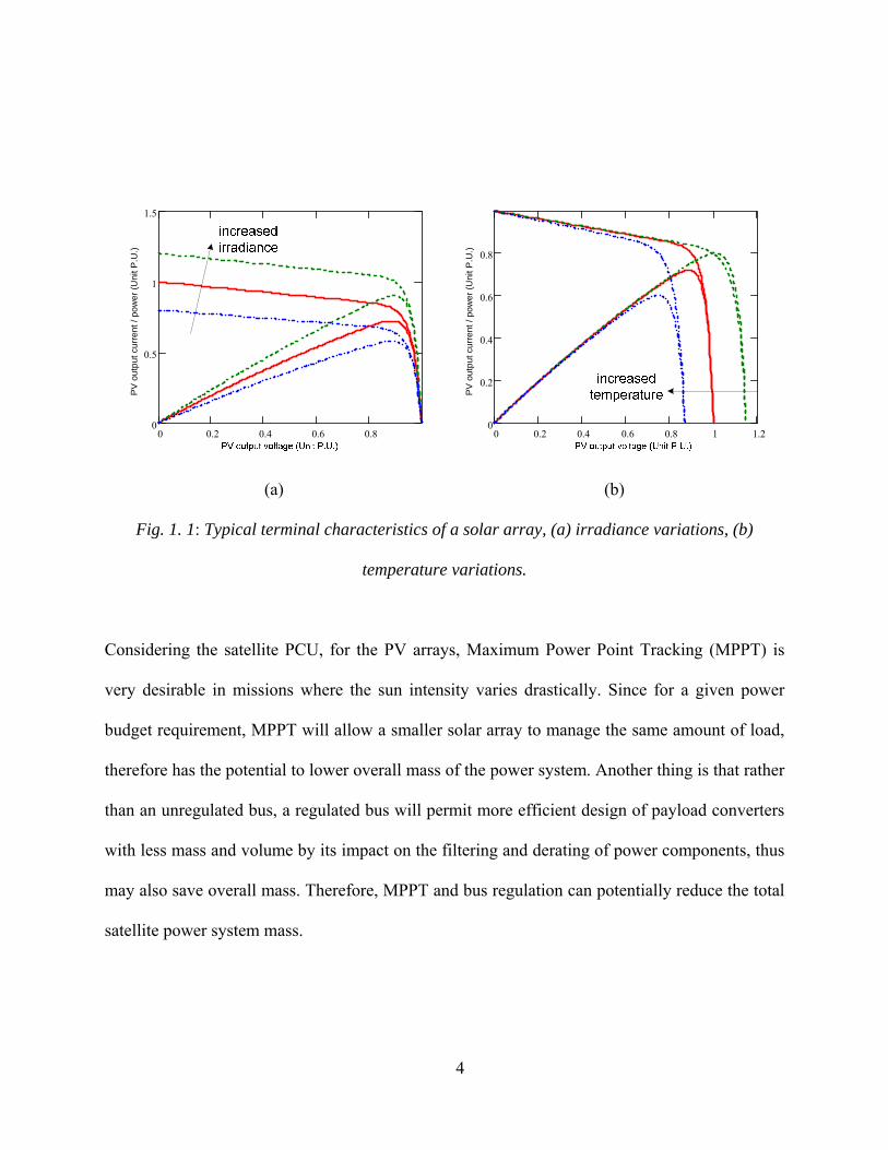
LIST OF FIGURES Fig. 1. 1: Typical terminal characteristics of a solar array, (a) irradiance variations, (b)
temperature variations. ................................................................................................... 4
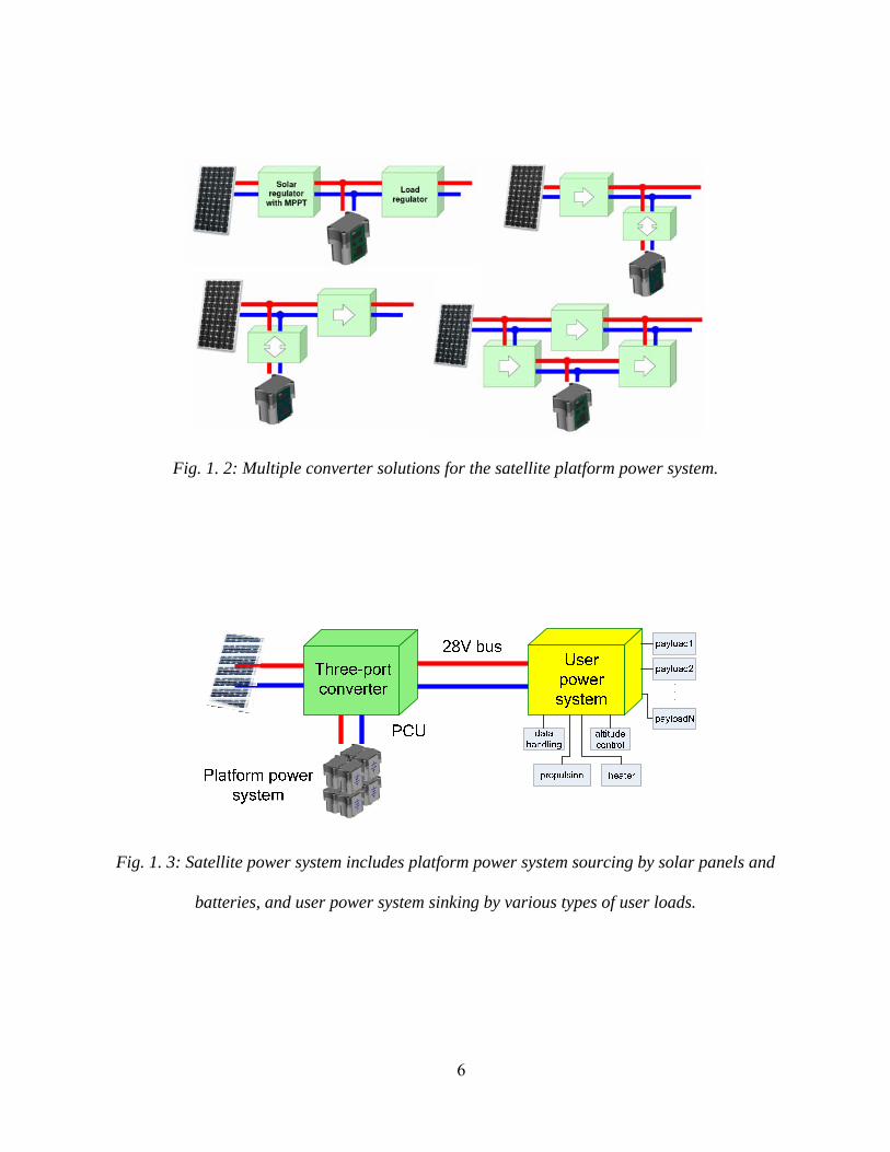
Fig. 1. 2: Multiple converter solutions for the satellite platform power system. ............................ 6
Fig. 1. 3: Satellite power system includes platform power system sourcing by solar panels
and batteries, and user power system sinking by various types of user loads. .............. 6
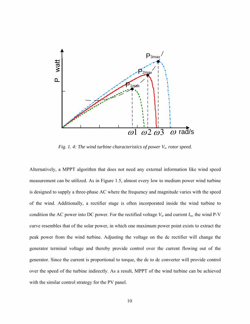
Fig. 1. 4: The wind turbine characteristics of power Vs. rotor speed. ........................................... 10
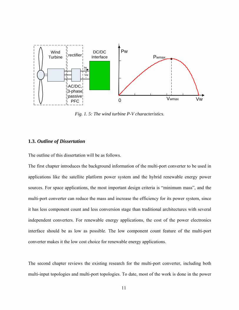
Fig. 1. 5: The wind turbine P-V characteristics. ........................................................................... 11
Fig. 2. 1: Multi-input buck-boost converter .................................................................................. 16
Fig. 2. 2: Multi-input flyback converter........................................................................................ 17
Fig. 2. 3: Multi-input flyback converter with a multi-winding transformer ................................. 18
Fig. 2. 4: Two-input current-fed full-bridge dc/dc converter ........................................................ 19
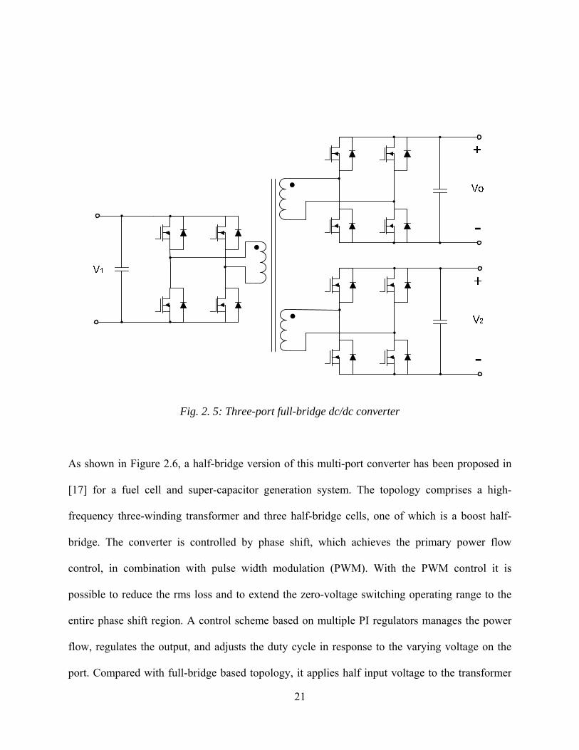
Fig. 2. 5: Three-port full-bridge dc/dc converter .......................................................................... 21
Fig. 2. 6: Three-port half-bridge dc/dc converter ......................................................................... 22
Fig. 2. 7: Triple-half-bridge bidirectional dc/dc converter ........................................................... 23
Fig. 2. 8: Reduced part, triple-half-bridge bidirectional dc/dc converter ..................................... 24
Fig 3. 1: Three-port modified half-bridge converter topology, which can achieve ZVS for
all three main switches (S1, S2, S3) and adopt synchronous rectification for the
secondary side to minimize conduction loss. ............................................................... 28
Fig 3. 2: Steady state waveforms of the three-port half-bridge converter .................................... 30

xii
Fig 3. 3: Operation stages of the three-port half-bridge converter ............................................... 35
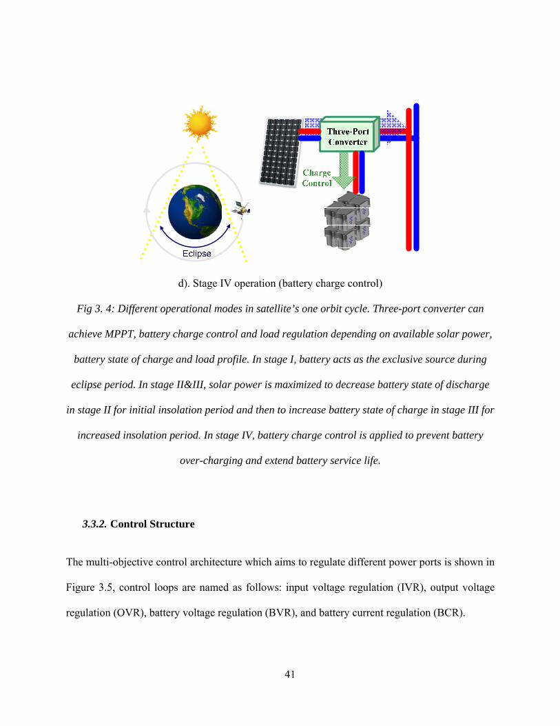
Fig 3. 4: Different operational modes in satellite’s one orbit cycle. Three-port converter
can achieve MPPT, battery charge control and load regulation depending on
available solar power, battery state of charge and load profile. In stage I,
battery acts as the exclusive source during eclipse period. In stage II&III, solar
power is maximized to decrease battery state of discharge in stage II for initial
insolation period and then to increase battery state of charge in stage III for
increased insolation period. In stage IV, battery charge control is applied to
prevent battery over-charging and extend battery service life. .................................... 41
Fig 3. 5: Three-port converter’s control architecture to achieve MPPT for solar port,
battery charge control for battery port and meanwhile always maintaining
voltage regulation for output port. OVR is to control d1, and the rest of control
loops (BVR, BCR and IVR) are competing the minimum value to control d2. ........... 42
Fig 3. 6: (a) Conventional mode transition algorithm flow chart which is inclined to
cause oscillation; (b) Oscillation between Mode 1 and Mode 2 because of
instant switching of duty cycle value ........................................................................... 45
Fig 3. 7: (a) the proposed minimum function competitive method to allow smooth
transition of modes; (b) Mode 1 to Mode 2 transition with no oscillation; (c)
Mode 2 to Mode 1 transition with no oscillation. ........................................................ 47
Fig 3. 8: Basic waveforms of the three-port converter. vpri and iLo represent transformer
primary side voltage and output inductor current, respectively. .................................. 49

xiii
Fig 3. 9: (a) Model comparison due to duty cycle step, (b) Averaged model and circuit
model comparison for Battery-regulation Mode. ......................................................... 54
Fig 3. 10: Small signal model of Battery-regulation Mode, control inputs and outputs are
decoupled to enable separate controller design. Voref and Vbref are the
references for output voltage and battery voltage, respectively. HOVR and HBVR
are the compensators need to be designed. .................................................................. 55
Fig 3. 11: Simulated bode plots for Battery-regulation Mode, (a) Vo(s)/ d1(s); (b) Vb(s)/
d2(s). Dashed line denotes open loop plant transfer function before applying
the compensator, solid line denotes close loop transfer function after applying
the compensator. BVR loop bandwidth is set to be one tenth of that of OVR. ........... 58
Fig 3. 12: Averaged model and circuit model comparison for Battery-balanced Mode ............... 60
Fig 3. 13: Small signal model of Battery-balanced Mode, control inputs and outputs are
decoupled to enable separate controller design. Voref and Vinref are the
references for output voltage and input voltage, respectively. HOVR and HIVR
are the compensators need to be designed. .................................................................. 60
Fig 3. 14: Simulated bode plots of Vin(s)/ d2(s). Dashed line denotes open loop plant
transfer function before applying the compensator, solid line denotes close
loop transfer function after applying the compensator. ............................................... 62
Fig 3. 15: Prototype photo of three-port converter which consists of one controller board
and one power board. ................................................................................................... 63
Fig 3. 16: Loading output port when the battery current is zero ................................................... 64
Fig 3. 17: Loading battery port when the output current is zero ................................................... 64

xiv
Fig 3. 18: ZVS for S1 .................................................................................................................... 65
Fig 3. 19: ZVS for S2 .................................................................................................................... 65
Fig 3. 20: ZVS for S3 .................................................................................................................... 66
Fig 3. 21: The efficiency when the power is transferred from solar port to output port ............... 67
Fig 3. 22: The efficiency when the power is transferred from solar port to battery port .............. 67
Fig 3. 23: The efficiency when the power is transferred from battery port to output port ........... 68
Fig 3. 24: Autonomous mode transition, (a) Mode 1 to Mode 2; (b) Mode 2 to Mode 1 ............. 70
Fig 3. 25: Simulated and measured bode plots, (a) Vo / d1, (b) Vb / d2, (c) Vin / d2 ...................... 72
Fig 3. 26: (a) Battery-regulation Mode load step response, (b) Battery-balanced Mode
load step response. ....................................................................................................... 74
Fig 3. 27: Different mode operations based on available solar power, battery state of
charge and load profile, left column shows four stages in satellite’s one orbit
cycle; for the right column, top one shows input solar panel voltage and
current, middle one represents battery voltage and current, bottom one shows
output port load level while its voltage is maintaining regulated all the time. ............ 76
Fig.4. 1: Paralleled three-port converter system interfacing solar panel, battery pack and
bus. ............................................................................................................................... 78
Fig.4. 2: Dual loop CS control structure ....................................................................................... 79
Fig.4. 3: Outer voltage loop and inner CS loop control structure ................................................. 80
Fig.4. 4: Inner voltage loop and outer CS loop control structure ................................................. 80

xv
Fig.4. 5: Loop analysis of output port with two paralleled converters, Gid and Gvd are
already obtained from section II (battery port control loop diagram is similar
with output port) ........................................................................................................... 84
Fig.4. 6: Calculated bode plots of output port control loops ........................................................ 85
Fig.4. 7: Bode plots of CS loop gain Tcs, stable and unstable ..................................................... 86
Fig.4. 8: Transient response to load steps from 40% to 100%, (a) stable CS loop gain Tcs;
(b) unstable CS loop gain Tcs’ ..................................................................................... 87
Fig.4. 9: Battery two stage charging profile ................................................................................. 89
Fig.4. 10: Solar array irradiance changes, then battery charging power changes
accordingly ................................................................................................................... 89
Fig.4. 11: Load level changes, then battery charging power changes accordingly ...................... 90
Fig.4. 12: Battery output model with droop resistances ............................................................... 91
Fig.4. 13: Effect of different droop rate on CS error (a) undesirable (b) acceptable (c)
good, zero error at 50% (d) good, zero error at 100% ................................................. 93
Fig.4. 14: Battery charging algorithm with CS ............................................................................. 94
Fig.4. 15: Input port current sharing diagram ............................................................................... 95
Fig.4. 16: Perturb&Observe MPPT algorithm with CS ................................................................ 96
Fig.4. 17: Prototype photo of two paralleled converters sharing with one DSP controller
board, each power stage is rated at 200W, input port and battery port has the
same ground while output port is isolated. .................................................................. 97
Fig.4. 18: Test setup with two paralleled three-port converters ................................................... 98
Fig.4. 19: Steady state waveforms for output inductor current and switching node voltage ........ 99

xvi
Fig.4. 20: Current sharing performance before and after CS function enabled ............................ 99
Fig.4. 21: Current sharing performance before and after CS function enabled .......................... 100
Fig.4. 22: Output port load sweep (0.5-14A) .............................................................................. 100
Fig.4. 23: Battery port load sweep (0.5-11A) ............................................................................. 101
Fig.4. 24: Battery load transient (1-5.5A) ................................................................................... 101
Fig.4. 25: Measured bode plots of output port (Tv and Tsys agree with each other) ................... 102
Fig.4. 26: Measured bode plots of battery port, droop CS does not affect BVR loop ................ 103
Fig.4. 27: Multi-channel converter structure .............................................................................. 104
Fig.4. 28: CS results with different approaches: (a) no current sharing, (b) active current
sharing, (c) droop current sharing. ............................................................................. 106
Fig.4. 29: Output port hybrid CS structure ................................................................................. 107
Fig.4. 30: Thevenin equivalent circuit ........................................................................................ 107
Fig.4. 31: Output impedance with (a) hybrid CS and (b) droop CS method. ............................. 110
Fig.4. 32: CS simulation results; (a) hybrid CS method, (b) droop CS method. ........................ 111
Fig.4. 33: Implementation of synchronization with no wires: (a) circuit block diagram; (b)
waveforms .................................................................................................................. 113
Fig.4. 34: Signal synchronization, (a) without synchronization; (b) with synchronization ........ 114
Fig.4. 35: Prototype photo of two converter channels ................................................................ 115
Fig.4. 36: Output port CS performance: (a) droop CS; (b) hybrid CS with better transients.
.................................................................................................................................... 116
Fig.4. 37: One channel fails while the other channel is not affected. ......................................... 117
Fig.4. 38: Input Port CS with MPPT .......................................................................................... 118

xvii
Fig.4. 39: Autonomous mode transitions: (a) both with MPPT; (b) transit from both with
MPPT to one with MPPT ; (c) transit from one with MPPT to both without
MPPT. ........................................................................................................................ 119
Fig. 5. 1: Four-port converter concept ........................................................................................ 121
Fig. 5. 2: The four-port half-bridge converter topology, which can achieve ZVS for all
four main switches (S1, S2, S3 and S4) and adopts synchronous rectification
for the secondary side to minimize conduction loss. ................................................. 122
Fig. 5. 3: The proposed modulation scheme: (a) PWM modulation circuits; (b) driving
signal key waveforms. ................................................................................................ 124
Fig. 5. 4: Steady state waveforms of the four-port half-bridge converter. .................................. 127
Fig. 5. 5: Operation stages of the four-port half-bridge converter .............................................. 133
Fig. 5. 6: A possible control structure to achieve MPPT for the PV panel and the wind
turbine, meanwhile maintaining output voltage regulation. OVR, SVR and
WVR loops are to control d1, d2 and d3, respectively. ............................................... 142
Fig. 5. 7: Small signal model diagram, control inputs and outputs are decoupled to enable
separate controller design. The far right signals are routed to the far left ones in
this diagram. Vsref, Vwref and Voref are the references for solar, wind and output
voltages, respectively. HSVR, HWVR and HOVR are the compensators need to be
designed. .................................................................................................................... 145
Fig. 5. 8: Steady state waveforms: (a) Loading the output port when the battery current is
zero; (b) Loading the battery port when the output current is zero. ........................... 149

xviii
Fig. 5. 9: Vgs and Vsw of the switch S1 ....................................................................................... 150
Fig. 5. 10: Vgs and Vsw of the switch S2 ..................................................................................... 150
Fig. 5. 11: Solar port, wind port, output port voltages under different load/source
conditions. .................................................................................................................. 152
Fig. 5. 12: Efficiency under different load/source conditions .................................................... 152
Fig. 5. 13: Transient response of solar, wind and output voltages when the load is
perturbed by a step change between 10% and 90% rated output current. .................. 154
Fig. 5. 14: OVR loop bode plots: (a) prediction; (b) experiment. .............................................. 154
Fig. 5. 15: SVR loop bode plots: (a) prediction; (b) experiment. ............................................... 155
Fig. 5. 16: WVR loop bode plots: (a) prediction; (b) experiment. .............................................. 155
Fig. 5. 17: Extension of the proposed multi-port DC/DC converter ........................................... 156

xix
LIST OF TABLES
Table 2.1 Comparison of Conventional Structure and Integrated Structure ................................. 15
Table 3.1 Values of Circuit Parameters ........................................................................................ 63
Table 5.1 Operational Stages of the Four-port Converter ........................................................... 140
Table 5.2 Different Load/Source Current Level Conditions ...................................................... 151

1
CHAPTER 1: INTRODUCTION
This chapter introduces the background information for the proposed multi-port converter to be
used in satellite applications and renewable energy applications.
1.1. Background for Satellite Applications
The ever-increasing cost of launching a spacecraft into space, approximately $100,000/kg, is a
major driving force behind the efforts to minimize the volume and weight of its power system.
Take the international space station as an example, the cost of the solar arrays per kilowatt is
over $3M/kW, assuming a mass of the solar array wing of 1000 kg and a beginning-of-life power
of 32 kW[3]. In other words, the cost is heavily determined by the mass. Moreover, it is
generally accepted that the satellite platform power system constitutes about 25% of its total dry
mass, and reaches a figure of 35% when the user power system is included[1]. Therefore, mass is
one of the most important design constraints for the space power system.
The satellite platform power system consists of solar arrays, batteries and an interface power
conditioning unit (PCU). The PCU then connects the solar arrays and batteries to a distribution
bus, normally 28V in low earth orbital (LEO) applications. The distribution bus then delivers the
power to the user power system which includes various user loads such as propulsion, altitude
control and data handling, etc.

2
The solar arrays generate the electrical power during periods of solar insolation throughout the
operational life of the satellite, and deliver the sufficient power to supply normal satellite bus,
which payloads the power demands. As mentioned above, the solar array is extremely heavy and
expensive; therefore, one major issue is to efficiently convert this solar energy into a type of
electrical energy that can be used by various loads.
Normally, there are two steps in the solar energy conversion.
The first step is to convert solar energy into an uncontrolled electrical power; its efficiency and
mass is strongly dependent on the solar array materials and the efficiency improvement is relying
on the development of material engineering, therefore it is beyond the scope of the power
electronics research.
The second step is to use a power electronics circuit or interface to convert the uncontrolled
power into a controlled and usable electrical power which can drive a distribution bus. The
second conversion step relies on power electronics engineers to come up with smart solutions to
achieve the power management control, with low mass and high efficiency.
The terminal voltage-current relationship of a PV cell can be described by the following
equation.
(exp[ / ( )] 1) /photo o series shuntI I I q A K T V I R V R= − ⋅ ⋅ ⋅ ⋅ + ⋅ − − Eq. 1.1
Where Iphoto: the photo current generated due to insolation
Io: the reverse saturation current of semiconductor material
Rseries: the series ohmic resistance of the cell

3
Rshunt: the leakage current
K: the boltzman’s constant
T: the absolute operating temperature
q: the charge of a single electron
A: the ideality factor of the p-n junction.
Figure 1.1 shows the typical nonlinear terminal characteristics of a solar array at different
operating conditions. For certain irradiance levels and temperatures, each PV curve has a point
that can deliver the maximal power. This point is defined as the maximum power point.
However, this point continuously moves following the variations in irradiance, temperature, and
other operating conditions. Therefore, a power electronics interface needs to be installed to
change the PV’s load characteristics and to force the PV panel to follow this point which can
maximize the solar power harvesting.
4
0 0.2 0.4 0.6 0.8 1 1.20
0.2
0.4
0.6
0.8
0 0.2 0.4 0.6 0.80
0.5
1
1.5
PV
out
put c
urre
nt /
pow
er (U
nit P
.U.)
PV
out
put c
urre
nt /
pow
er (U
nit P
.U.)
(a) (b)
Fig. 1. 1: Typical terminal characteristics of a solar array, (a) irradiance variations, (b)
temperature variations.
Considering the satellite PCU, for the PV arrays, Maximum Power Point Tracking (MPPT) is
very desirable in missions where the sun intensity varies drastically. Since for a given power
budget requirement, MPPT will allow a smaller solar array to manage the same amount of load,
therefore has the potential to lower overall mass of the power system. Another thing is that rather
than an unregulated bus, a regulated bus will permit more efficient design of payload converters
with less mass and volume by its impact on the filtering and derating of power components, thus
may also save overall mass. Therefore, MPPT and bus regulation can potentially reduce the total
satellite power system mass.

5
On the other hand, the battery will provide electrical energy to the satellite during pre-launch
operations, the launch phase, eclipse periods, and during periods of peak power demand that
exceeds solar array output capability. The battery needs to be protected from both over-charging
and over-discharging in order to extend its service lifespan. So battery protection is always
necessary for the satellite power system.
However, in the traditional satellite power system architectures as shown in Figure 1.2, normally
several independent converters are used to achieve MPPT for the solar panel, battery
charging/discharging control and bus regulation at the expense of increased conversion steps and
control complexity. The added complexity, together with increased losses, size, weight, and cost,
as well as decreased reliability, has impeded wide-spread adoption of such architectures for the
satellite PCU. The potentially profitable MPPT technology has often been difficult to justify
given the mass of MPPT regulator and control complexity overhead. Therefore, as in Figure 1.3,
a single conversion stage is proposed in this dissertation to efficiently achieve MPPT and battery
regulation while always maintaining a regulated distribution bus. The multi-functional utilization
of power processing components and integration of control tasks reduces the size, weight, cost,
and complexity, making the three-port converter a good candidate for the satellite platform
power system.
6
Fig. 1. 2: Multiple converter solutions for the satellite platform power system.
Fig. 1. 3: Satellite power system includes platform power system sourcing by solar panels and
batteries, and user power system sinking by various types of user loads.

7
1.2. Background for Renewable Energy Applications
Recently, renewable energy sources such as PV arrays, wind generators and fuel cells are gaining
more and more attention due to their advantage of being abundant in nature and causing zero-
emissions. For solar energy and wind energy, they are now the world’s fastest growing energy
resources. Today’s PV arrays and wind turbines are state-of-the-art of modern technology, with
modular design and quick installation. Since these renewable sources are intermittent in nature,
combining more than one renewable source can increase the certainty of continuous load
supplying compared with the individual source because of the renewable sources’
complementary feature.
In order to accommodate different types of renewable sources, a multi-port converter interface
will be desirable to achieve the power management control among different power sources and
loads, and a storage device is necessary when the ac mains is not available. Otherwise, using
several independent traditional converters will increase the total cost for the renewable system,
because of high component count and increased control complexity. Therefore, the multi-port
converter is a great fit for applications with hybrid renewable sources requiring low cost
solutions.
For example, PV and wind power are complementary since sunny days are usually calm, and
strong winds often occur on cloudy days or at night time. Moreover, the optimum combinations
of PV array size and wind turbine capacity can be selected based on the solar and wind profile of
the installation site to achieve the lowest cost per kilowatt of power. In order to keep supplying

8
power to the load in case no solar or wind power is available, a storage device has to be installed,
which necessitates at least one bidirectional port from a multi-port interface. For the system level
control strategy, in its normal operation, MPPT of both solar and wind will be desired while
maintaining a regulated output, since MPPT can ensure maximum power harvesting. In addition,
a battery will collect surplus power at light loading, and supply the deficit power at heavy
loading. Therefore, the solar and wind sources can be scaled to deliver the average load while the
battery supplies power during peak load period. As a result, PV array and wind turbine
requirement is low and the initial installing cost is reduced as well.
The PV array characteristics have been introduced in the above section; in this section we will
discuss the wind energy characteristics. A wind turbine can be defined as a machine that takes
kinetic energy from the wind and converts it to mechanical energy and transfers the motion to an
electric generator shaft. The fundamental equation governing the mechanical power capture of
the wind turbine rotor blades, which drives the electrical generator, is given by:
312 PP AC Vρ= Eq. 1.2
Where ρ : Air density (kg/m3)
A: Area swept by the rotor blades
V: Velocity of air (m/sec)
Cp.: Power coefficient of the wind turbine.

9
The theoretical maximum value of the power coefficient Cp is 0.59 and it is often expressed as
the function of the rotor tip-speed to wind-speed ratio TSR. TSR is defined as the linear speed of
the rotor to the wind speed.
RTSRVω
= Eq. 1.3
Where R andω are the turbine radius and the angular speed, respectively. In practical designs,
the maximum achievable wind turbine efficiency Cp ranges between 0.4 and 0.5 for modern high
speed turbines and between 0.2 and 0.4 for slow speed turbines.
The typical power Vs. rotor speed curve is plotted in Fig 1.4. As can be seen, there is a maximum
power point at a certain rotor speed. For the wind turbine, the maximum power for different wind
speeds is generated at different rotor speeds. Therefore, the turbine speed should be controlled to
follow an optimal operating point which is different for every wind speed. For some designs, this
is achieved by incorporating a speed control in the system design to run the rotor at high speed in
high wind and at low speed in low wind, resulting in maximum electrical energy generation.
Unfortunately, accurate wind speed measurement in the rotor of the turbine is difficult and
requires the use of a relatively expensive anemometer if it is to be used for system control.
10
ω rad/s1ω 2ω 3ω
P1max
P3max
P2max
Fig. 1. 4: The wind turbine characteristics of power Vs. rotor speed.
Alternatively, a MPPT algorithm that does not need any external information like wind speed
measurement can be utilized. As in Figure 1.5, almost every low to medium power wind turbine
is designed to supply a three-phase AC where the frequency and magnitude varies with the speed
of the wind. Additionally, a rectifier stage is often incorporated inside the wind turbine to
condition the AC power into DC power. For the rectified voltage Vw and current Iw, the wind P-V
curve resembles that of the solar power, in which one maximum power point exists to extract the
peak power from the wind turbine. Adjusting the voltage on the dc rectifier will change the
generator terminal voltage and thereby provide control over the current flowing out of the
generator. Since the current is proportional to torque, the dc to dc converter will provide control
over the speed of the turbine indirectly. As a result, MPPT of the wind turbine can be achieved
with the similar control strategy for the PV panel.
11
Wind Turbine
AC/DC, 3-phase passive
PFC
rectifier
Vw+
-
Iw
Vw
Pw
Vwmax
PwmaxDC/DC
Interface
0
Fig. 1. 5: The wind turbine P-V characteristics.
1.3. Outline of Dissertation
The outline of this dissertation will be as follows.
The first chapter introduces the background information of the multi-port converter to be used in
applications like the satellite platform power system and the hybrid renewable energy power
sources. For space applications, the most important design criteria is “minimum mass”, and the
multi-port converter can reduce the mass and increase the efficiency for its power system, since
it has less component count and less conversion stage than traditional architectures with several
independent converters. For renewable energy applications, the cost of the power electronics
interface should be as low as possible. The low component count feature of the multi-port
converter makes it the low cost choice for renewable energy applications.
The second chapter reviews the existing research for the multi-port converter, including both
multi-input topologies and multi-port topologies. To date, most of the work is done in the power

12
stage design and topology investigation, with only a few reports focusing on the control aspects
such as modeling and control strategies for the multi-port converter, which is actually very
challenging for such kinds of multi-input multi-output systems. This dissertation is going to
focus on not only the topology investigation, but also the control aspects.
The third chapter discusses the design of a three-port converter for space applications. First, the
circuit operation and power stage design considerations are introduced, including the various
circuit stages, ZVS analysis and DC analysis, etc. Then, the control aspects, such as various
modes of operation and the autonomous mode transitions are discussed. This chapter also
proposes a modeling procedure suitable for the multi-port converter based on the traditional
state-space averaging method advocated by Dr. Middlebrook and Dr. Cuk [4], [5]. The major
difference is that for the proposed method, different modes need to be identified first for the
multi-port converter, and then the corresponding state variables need to be chosen to reveal the
dynamic characteristics of the power ports that are of interest. Finally, the state-space equations
in each main circuit stages are averaged to derive the converter model which follows the
traditional state-space averaging method. Since control loops are coupled with each other due to
the power stage integration issue, the proper decoupling method is suggested to allow separate
controller design for each power port. The modeling procedure is general and is designed to be
suitable for other multi-port topologies.
The fourth chapter talks about the interesting topic of paralleled multi-port converters. The main
difficulty for designing current sharing controllers for multi-port converters is that there are so

13
many control loops involved, and the adding of the current sharing controller should not
adversely affect the system stability and needs to achieve good current sharing performance, both
in steady state and dynamics. Also, the added current sharing function should still preserve the
attractive features like MPPT and battery charging. First, the current sharing for two three-port
converters are introduced, and then followed by the current sharing for multiple three-port
converter channels. A dual loop current sharing control structure is identified to be suitable for
such a multi-input multi-output system, because the voltage loop and current loop can be
assumed to be decoupled to simplify the control loop design. A hybrid current sharing strategy
combining the active and passive control methods is proposed to achieve good current sharing
dynamic performance and avoid the current sharing bus that would be present for the active
current sharing method.
The fifth chapter proposes a novel four-port half-bridge converter for renewable energy
applications. The four-port topology is constructed by simply adding two switches and diodes to
the traditional half-bridge topology. Moreover, zero-voltage switching (ZVS) can be achieved
for all main switches to allow higher efficiency at higher switching frequency, which will lead to
more compact design of this multi-port converter. The circuit operation and topology is
introduced first, including the driving scheme, ZVS analysis, steady state analysis,
semiconductor stress consideration, etc. Three of the four ports can be tightly regulated by
adjusting their independent duty cycle values, while the forth port is left unregulated to maintain
the power balance for the system. The control structure targeting the hybrid solar wind
application is proposed to allow MPPT of both the PV panel and the wind turbine simultaneously

14
or individually and then its small-signal model is derived by the modeling procedure proposed in
the third chapter. Finally, a prototype is built to verify the proposed topology and confirm its
ability to achieve tight independent control over three power processing paths.
The sixth chapter gives the conclusion and the scope of future work.

15
CHAPTER 2: LITERATURE REVIEW
Advantages of the integrated multi-port converter instead of several independent converters such
as less component count and conversion stage can be obtained because resources of switching
devices and storage elements are shared in each switching period. As a result, the integrated
system will have a lower overall mass and more compact packaging. In addition, some other
advantages of integrated power converters are lower cost, improved reliability, and enhanced
dynamic performance due to power stage integration and centralized control. Additionally, it
requires no communication capabilities that would be necessary for multiple converters.
Therefore, the communication delay and error can be avoided with the centralized control
structure. Instead of one control input for traditional two-port converter, N-port converter has N-
1 control inputs, which makes the multi-port converter difficult to be modeled. Moreover, since
the multi-port converter has an integrated power stage and thus the Multi-Input Multi-Output
(MIMO) feature, it necessitates proper decoupling for various control loops design. Table 1 gives
a comparison of the two different system structures.
Table 2.1 Comparison of Conventional Structure and Integrated Structure
Conventional multi-converter structure Integrated multi-port structure Conversion stage more than one One Component count high Low Overall mass high Low Control design conventional and well-known complicated and little-reported Control structure separated (require communication) centralized (no communication)Control input one N-1 Control loop decoupling not required Necessary * N denotes the port numbers of N-port integrated converter.

16
Since most of the existing researches are conducted in the area of the topology investigation, the
following literature review will focus on the features of different topologies.
2.1. Multi-input Converters
As shown in Figure 2.1, a multi-input integrated buck-boost topology is proposed in [10] to
allow multiple input sources. The topology is capable of interfacing sources of different voltage-
current characteristics to a common load, while achieving a low component count. The open-
loop circuit operation has been investigated to prove that the output port can be regulated based
on the duty cycle value control of the active unidirectional switches. The operation modes of
both continuous conduction mode (CCM) and discontinuous conduction mode (DCM) have been
analyzed to obtain voltage gain relations. However, the output voltage is reversed with regard to
input, and it is a non-isolated topology, which can not meet the isolation requirement for certain
critical applications.
Fig. 2. 1: Multi-input buck-boost converter

17
Hence, an isolated version of the above-mentioned topology named as multi-input flyback
converter has been proposed in [11], which is illustrated in Figure 2.2. The output voltage
polarity is the same as input, and output isolation is achieved. It is shown mathematically that the
idealized converter can accommodate arbitrary power commands for each input source while
maintaining a prescribed output voltage. Power budgeting is demonstrated experimentally for a
real converter under various circumstances, including a two-input (solar and line-powered)
system. A closed-loop control example involving simultaneous tracking of output voltage and
set-point tracking of the solar array shows that an autonomous system is realizable.
V1
V2
VN
Vo+
Fig. 2. 2: Multi-input flyback converter
This simple winded transformer in [11] can be replaced by a multi-winding transformer in [20]
to allow more flexible input voltage range. This topology as shown in Figure 2.3 is used for a
zero-emission electric power generation system that has two input sources: one solar source and
one ac mains input. The steady state and dynamic characteristics of this converter has been
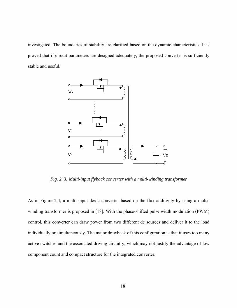
18
investigated. The boundaries of stability are clarified based on the dynamic characteristics. It is
proved that if circuit parameters are designed adequately, the proposed converter is sufficiently
stable and useful.
Fig. 2. 3: Multi-input flyback converter with a multi-winding transformer
As in Figure 2.4, a multi-input dc/dc converter based on the flux additivity by using a multi-
winding transformer is proposed in [18]. With the phase-shifted pulse width modulation (PWM)
control, this converter can draw power from two different dc sources and deliver it to the load
individually or simultaneously. The major drawback of this configuration is that it uses too many
active switches and the associated driving circuitry, which may not justify the advantage of low
component count and compact structure for the integrated converter.
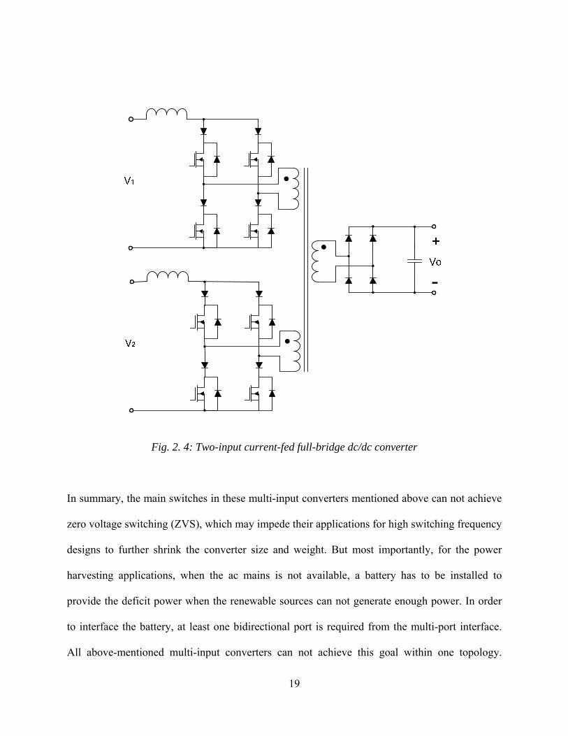
19
Fig. 2. 4: Two-input current-fed full-bridge dc/dc converter
In summary, the main switches in these multi-input converters mentioned above can not achieve
zero voltage switching (ZVS), which may impede their applications for high switching frequency
designs to further shrink the converter size and weight. But most importantly, for the power
harvesting applications, when the ac mains is not available, a battery has to be installed to
provide the deficit power when the renewable sources can not generate enough power. In order
to interface the battery, at least one bidirectional port is required from the multi-port interface.
All above-mentioned multi-input converters can not achieve this goal within one topology.

20
Therefore, multi-port converters having the bidirectional port are necessary to interface the
storage device.
2.2. Multi-port Converters
As shown in Figure 2.5, a three-port dc-dc converter has been proposed in [25] to have
bidirectional and also ZVS capabilities. It is based on full bridge cells that allow bidirectional
power flow in each port. Such a configuration facilitates the matching of different voltage levels
in the overall system by the multi-winding transformer. The transformer design was optimally
performed in order to incorporate the leakage inductances as required by the topology to affect
the phase shift control. Furthermore, for the three-port converter, a dual-PI-loop based control
strategy is proposed to achieve constant output voltage and power flow management. This
topology has been verified through a hybrid fuel cell and super-capacitor system to improve the
slow transient response of a fuel cell stack.
A similar work has been done in [24] taking the same topology to interface 14V and 42V bus to
the high voltage bus for hybrid electric vehicles (HEVs). Besides the phase shift control
managing the power flow between the ports, utilization of the duty cycle control for optimizing
the system behavior is discussed. The dynamic analysis and associated control design are
presented. A control-oriented converter model is developed and the bode plots of the control-
output transfer functions are given. A control strategy with the decoupled power flow
management is implemented to obtain fast dynamic response.
21
Fig. 2. 5: Three-port full-bridge dc/dc converter
As shown in Figure 2.6, a half-bridge version of this multi-port converter has been proposed in
[17] for a fuel cell and super-capacitor generation system. The topology comprises a high-
frequency three-winding transformer and three half-bridge cells, one of which is a boost half-
bridge. The converter is controlled by phase shift, which achieves the primary power flow
control, in combination with pulse width modulation (PWM). With the PWM control it is
possible to reduce the rms loss and to extend the zero-voltage switching operating range to the
entire phase shift region. A control scheme based on multiple PI regulators manages the power
flow, regulates the output, and adjusts the duty cycle in response to the varying voltage on the
port. Compared with full-bridge based topology, it applies half input voltage to the transformer
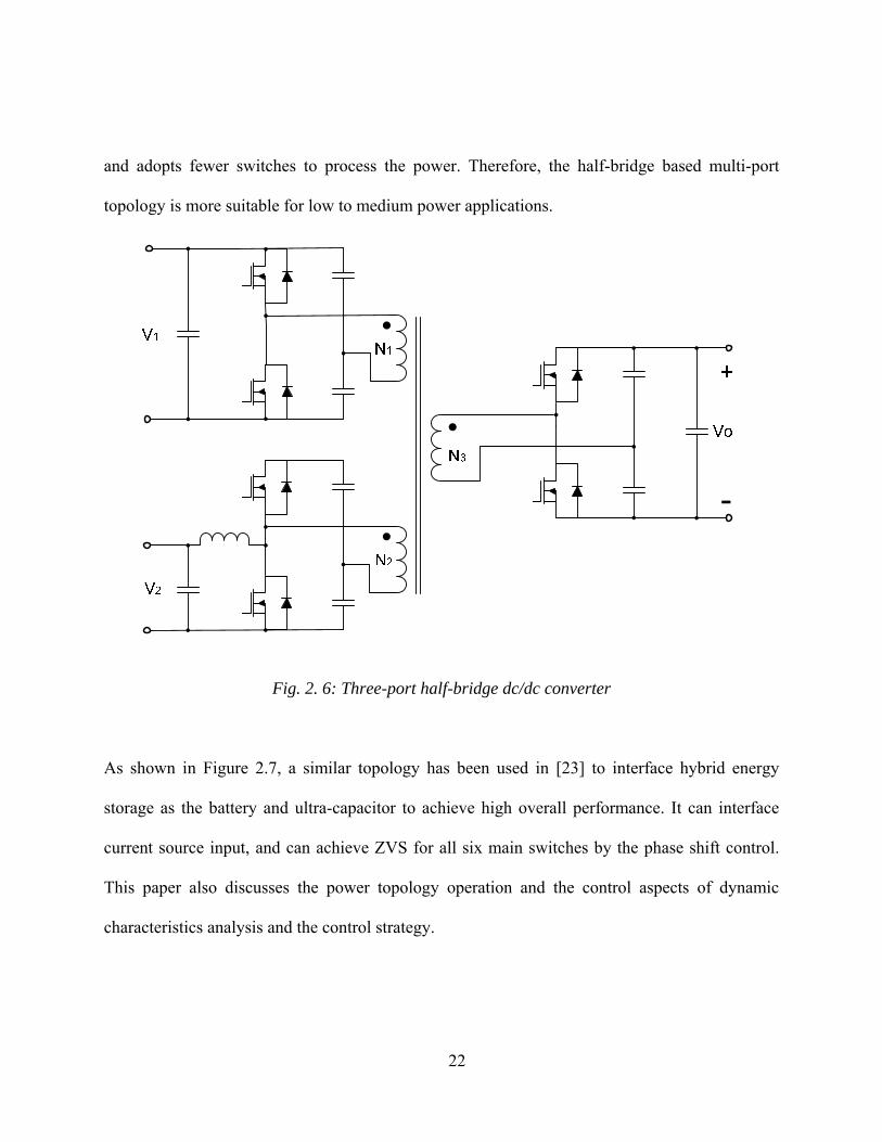
22
and adopts fewer switches to process the power. Therefore, the half-bridge based multi-port
topology is more suitable for low to medium power applications.
Fig. 2. 6: Three-port half-bridge dc/dc converter
As shown in Figure 2.7, a similar topology has been used in [23] to interface hybrid energy
storage as the battery and ultra-capacitor to achieve high overall performance. It can interface
current source input, and can achieve ZVS for all six main switches by the phase shift control.
This paper also discusses the power topology operation and the control aspects of dynamic
characteristics analysis and the control strategy.
23
V2
Vo
+
N2
N3
V1
N1
Fig. 2. 7: Triple-half-bridge bidirectional dc/dc converter
The above-mentioned topologies adopt a multi-winding transformer to couple different power
ports. Therefore, all ports are fully isolated with each other. However, some applications do not
require all ports to be fully isolated, and the share of some grounds may allow less component
and fewer transformer windings. As shown in Figure 2.8, a topology in [15] is intended for
future hybrid and fuel cell vehicles which may have three voltage nets: 14V, 42V and high
voltage (>200V) buses. A soft-switched dc-dc converter using four switches has been proposed
to interconnect these three nets. Its power flow management is based on a combined duty ratio
and phase shift control, but soft-switching range is limited when the phase shifts between two
very different voltage levels to have large current swing.

24
V1
Vo
V2
Fig. 2. 8: Reduced part, triple-half-bridge bidirectional dc/dc converter
To sum up, these multi-port topologies can be classified as two categories: non-isolated
topologies [6]-[14] and isolated topologies [15]-[28]. Non-isolated multi-port converters usually
take the form of buck, boost, buck-boost, etc, featuring compact design and high power density;
isolated multi-port converters using bridge topologies have the advantages of flexible voltage
levels and high efficiency since high frequency transformer and soft-switching techniques are
used. As well, isolation may be required for certain critical applications.
2.3. Summary
From the above literature review, all of the reported multi-port solutions suffer from at least one
of the following drawbacks:
1. Lack of bidirectional capability to interface the battery;
2. No isolation capability or having too many isolating power ports with a bulky multi-
winding transformer;

25
3. Using too many active switches and passive components which can not justify the multi-
port features like low component count and compact structure;
4. Lack of soft-switching capability to allow high frequency design to further shrink the
converter size;
5. The power among different power ports can not be transferred individually or
simultaneously.
For our applications, it requires at least one bidirectional port and only one isolated output port.
The topologies with all ports isolated are over-qualified and unnecessary for our application.
Therefore, the topologies with only one isolated port are sufficient. From this point of view, the
topology as shown in Figure 2.8 is a good candidate. But as mentioned above, it has four main
switches and its soft-switching range is limited when ports’ voltage change largely. Therefore the
main switches can still be reduced. Besides, our topology needs to have multiple input ports, but
all above-mentioned multi-input topologies do not have ZVS soft-switching capability to allow
high frequency designs. To sum up, the proposed topologies in this dissertation have the
following features:
1. Have bidirectional capability;
2. Have one isolation port;
3. Low component count: have N switches for the N-port converter, that is three switches for
a three-port converter;
4. ZVS for all main switches to allow high switching frequency designs;
5. The power among different power ports can be transferred individually or simultaneously.

26
For space applications in Chapter 3 and Chapter 4, the proposed three-port topology will have
only three main switches, and it can achieve soft-switching for all the main switches for a wide
input voltage range. Its main components are only three main switches, one clamping diode, one
transformer, two rectification diodes and one inductor. For renewable energy applications in
Chapter 5, based on the three-port converter, the proposed four-port topology adds one switch
and diode to incorporate one more input port while still achieving ZVS for all four main
switches. The power from both input ports can be transferred to the output port or battery port
individually or simultaneously. If only one input source is available, the four-port topology
reduces into the three-port operation which is almost the same as the topology proposed in
Chapter 3. In Chapter 5, the proposed topology is extended into interface N power ports while
still achieving ZVS for all main switches and still having very low component count. Therefore,
this topology is a valuable choice for both space applications requiring minimum mass and
renewable energy applications requiring minimum cost.

27
CHAPTER 3: AN INTEGRATED THREE-PORT DC/DC CONVERTER: CIRCUIT ANALYSIS, MODELING AND CONTROL
3.1. General Description
This chapter discusses the circuit operation, the modeling and the control of an integrated three-
port converter for space applications. From topology point of view, this new three-port topology
is derived by adding a diode and a switch across the transformer primary side, which provides
one more control freedom and ensures a clamping path for the leakage energy to create ZVS
condition for all the main switches. Since it is a new three-port converter, the small signal model
will be desired to achieve the close loop controller design. Especially for such kind of multi-
input multi-output (MIMO) control system, a precise model is critical to provide guidance
through the whole control design process. Moreover, since various control loops are cross
coupled with each other, a decoupling method suitable for such a MIMO system is proposed to
allow separate controller design for each power port’s feedback loop. The modeling procedure is
based on the traditional state-space averaging method, and is suitable to be applied for other
multi-port converters.
3.2. Circuit and Topology
This section introduces the three-port topology. As shown in Figure 3.1, it is a modified version
of PWM half bridge converter which includes three basic circuit stages within a constant-
frequency switching cycle to provide two independent control variables, namely duty-cycles d1
28
and d2 which are to control S1 and S2, respectively. This allows tight control over two of the
converter ports, while the third port provides the power balance in the system. The switching
sequence ensures a clamping path for the energy of the leakage inductance of the transformer at
all times. This energy is further utilized to achieve zero-voltage switching (ZVS) for all primary
switches for a wide range of source and load conditions. The circuit operation, the ZVS analysis
and the DC analysis will be discussed as follows.
Fig 3. 1: Three-port modified half-bridge converter topology, which can achieve ZVS for all
three main switches (S1, S2, S3) and adopt synchronous rectification for the secondary side to
minimize conduction loss.
3.2.1. Circuit Operation Principles
The steady-state waveforms of the three-port converter are shown in Figure 3.2, and the
operation stages in one switching cycle are shown in Figure 3.3.

29
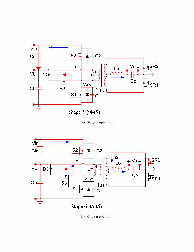
Stage 1 (t0-t1): Before this stage begins, the body diode of S1 is forced on to recycle the energy
in the transformer leakage inductor, and the output is freewheeling. At time t0, S1 is gated on
with ZVS, and then the leakage inductor is reset to zero and reverse-charged.
Stage 2 (t1-t2): At time t1, the transformer primary current increases to reflected current of io,
the body diode of SR2 is blocked, and the converter starts to deliver power to output.
Stage 3 (t2-t3): At time t2, S1 is gated off, causing the leakage current ip to charge C1 and
discharge C2.
Stage 4 (t3-t4): At time t3, the voltage across C2 is discharged to zero, and D2 conducts to carry
the current, which provides ZVS condition for S2. During this interval, the output is
freewheeling.
Stage 5 (t4-t5): At time t4, S2 is gated on with ZVS, and then the leakage inductor is reset to zero
and reverse-charged. Output inductor current drop between t2 and t5 is due to the leakage
inductor discharge/charge.
Stage 6 (t5-t6): At time t5, the transformer primary current increases to reflected current of i2,
the body diode of SR1 is blocked, and the converter starts to deliver power to output.
Stage 7 (t6-t7): At time t6, S2 is gated off, causing the leakage current ip to charge C2 and
discharge C1.
Stage 8 (t7-t8): At time t7, the voltage across D3 is discharged to zero, and D3 conducts. Since
S3 is gated on before this time, the leakage current freewheels through D3 and S3 so that the
leakage energy is trapped. On the secondary side, output inductor current freewheels through
SR1 and SR2.

30
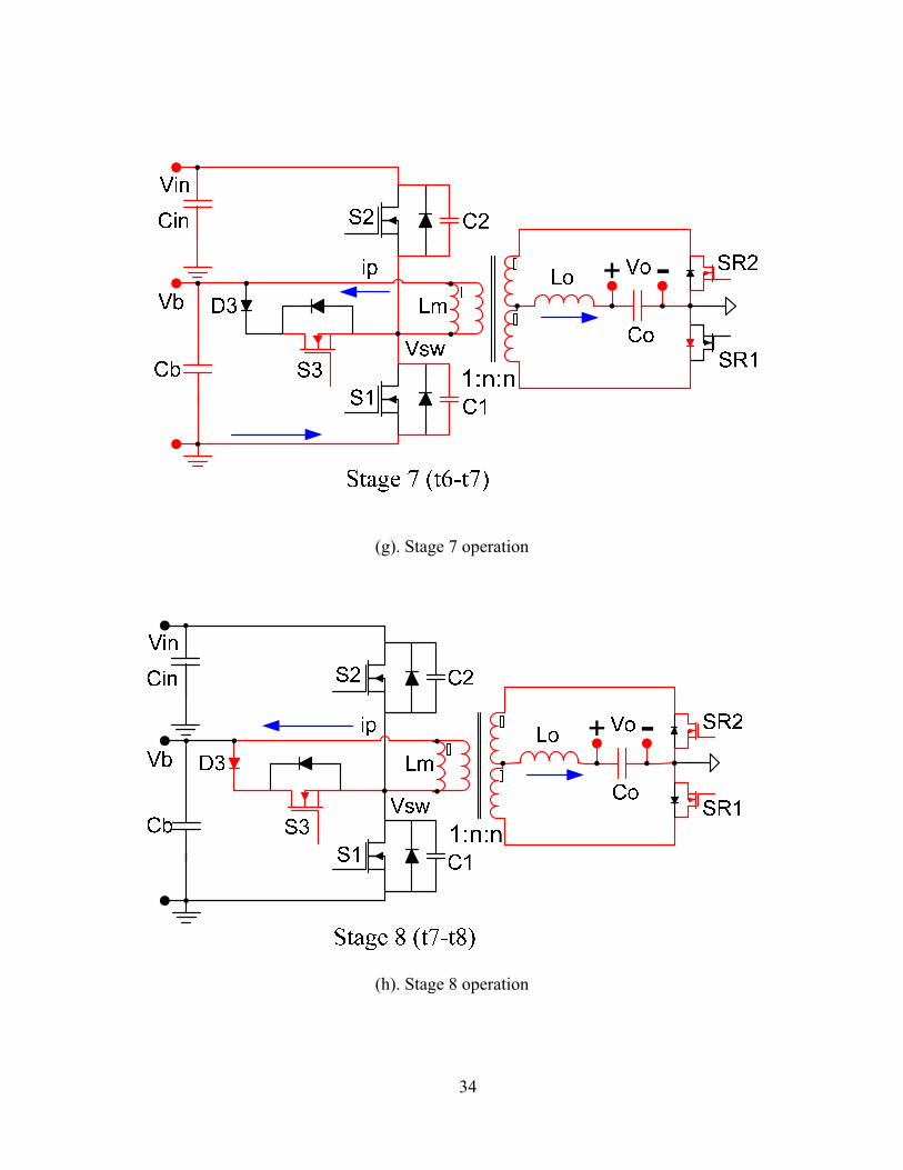
Stage 9 (t8-t9): At time t8, S3 is gated off, causing the trapped leakage energy to discharge C1
and charge C2.
Stage 10 (t9-t10): At time t9, the voltage across S1 is discharged to zero, and D1 conducts to
carry the current, which provides ZVS condition for S1. During this interval, the output is
freewheeling.
This is the end of the switching cycle.
Fig 3. 2: Steady state waveforms of the three-port half-bridge converter
31
S1S3
S2Cin
D3
1:n:n
Lo
Co
Vo
Vin
Vb
SR1
SR2
Lm�
�
�
C2
C1
Stage 1 (t0-t1)
ip
VswCb
(a). Stage 1 operation
S1S3
S2Cin
D3
1:n:n
Lo
Co
Vo
Vin
Vb
SR1
SR2
Lm�
�
�
C2
C1
Stage 2 (t1-t2)
Vsw
ip
i1Cb
(b). Stage 2 operation
32
(c). Stage 3 operation
(d). Stage 4 operation
33
(e). Stage 5 operation
(f). Stage 6 operation
34
(g). Stage 7 operation
(h). Stage 8 operation
35
S1S3
S2Cin
Cb
D3Lo
Co
Vo
Vin
Vb Lm�
�
�
SR2
SR11:n:n
C2
C1
Stage 9 (t8-t9)
Vsw
ip
(i). Stage 9 operation
(j). Stage 10 operation
Fig 3. 3: Operation stages of the three-port half-bridge converter

36
3.2.2. ZVS Analysis
When loading the output port, ZVS of the switches S1 and S2 can be realized through the energy
stored in the transformer leakage inductor, while ZVS of S3 is always maintained because D3
will be forced on when the switching node voltage Vsw is connected to the input voltage Vin.
After S3 is turned off, the leakage energy is released to discharge C1 and charge C2 and S3’s
parasitic capacitance C3. The following condition should be satisfied to achieve ZVS for S1:
2 2 21 1( ) ( ), 02 2k M o oss in bi M oL I n I C V V I n I⋅ ⋅ + ⋅ > ⋅ ⋅ + + ⋅ > Eq. 3.1
Where Lk is the transformer leakage inductance, Coss is the MOSFET parasitic capacitance of S1,
S2 and S3, Vin is the input voltage, Io is the output load current, IM is the transformer magnetizing
current which is determined by the following equation.
( )1 2
1 2
bi oM
I D D nII
D D+ −
=+
Eq. 3.2
After S1 is turned, the leakage energy may charge C1 and discharge C2 and S3’s parasitic
capacitance C3 to achieve ZVS for S2:
2 2 21 1( ) , 02 2k M o oss in oss bi M oL I n I C V C V I n I⋅ ⋅ − ⋅ > ⋅ + ⋅ ⋅ − ⋅ < Eq. 3.3
Where Ibi is the battery current. Therefore, when Io is small and IM is large, 0M oI n I− ⋅ < can not
be met, and ZVS of S2 is lost. Worst case scenario would be when loading the battery port and
leaving output port open, 0MI > , so ZVS of S2 can not be achieved.

37
3.2.3. DC Analysis
Assuming an ideal lossless converter, the steady-state voltage governing relations between
different port voltages can be determined by equating the voltage-second product across the
converter’s two main inductors to zero. First, using volt-second balance across the primary
transformer magnetizing inductance, when operating in continuous conduction mode (CCM), we
have:
1 2( )bi in biV D V V D⋅ = − ⋅ Eq. 3.4
With Vin = VC1 + VC2, and Vbi=VC1, the voltage at the bidirectional port, Vbi, may be given by:
2
1 2bi in
DV VD D
=+ Eq. 3.5
Where Vin is the voltage of the input port, D1 and D2 are the duty-cycles of S1 and S2,
respectively, and T is the duration of the switching cycle. Assuming CCM operation, the volt-
second balance across the load filter inductor yields:
( ) ( )1 2 1 2(1 ) 0bi o in bi o oDT nV V D T nV nV V D D TV− + − − − − − =
1 2
1 2
2o inD DV nV
D D=
+ Eq. 3.6
Where n is the turns ratio of the transformer, and Vo is the load-port voltage. Using Equation 3.5,
this can also be re-written as:
bio nVDV 12= Eq. 3.7
Assuming a lossless converter, steady-state port currents can be related by applying the power
conservation principle as follows:

38
oobibiinin IVIVIV += Eq. 3.8
Where Iin, Ibi, Io are the average input, bidirectional battery, and load currents, respectively.
3.3. Modeling and Control
This section introduces a modeling method specially tailored for deriving multi-port converter’s
small signal models under different modes of operation. A decoupling network is then introduced
to allow separate controller designs. Since there are various modes of operation, it is challenging
to define different modes and further to implement autonomous mode transition based on the
energy state of the three power ports. Various modes of operation are defined. And a competitive
method is used to realize smooth and seamless mode transition.
3.3.1. Mode Definition
Having different operational modes is one of the unique features for multi-port converters. As
illustrated in Figure 3.4, orbital satellite’s power platform experiences periods of insolation and
eclipse during each orbit cycle, with insolation period being longer. Since Maximum Power
Point Tracking (MPPT) can notably boost solar energy extraction of a photovoltaic (PV) system,
the longer insolation period means that MPPT is more often operated to allow a smaller solar
array while managing the same amount of load. Two assumptions are made to simplify analysis:
1) Load power is assumed to be constant; 2) Battery over-discharge is ignored because PV arrays

39
and batteries are typically over-sized in satellites to provide some safety margins. Four stages in
satellite’s one orbit cycle yield two basic operational modes as follows.
In Battery-balanced Mode (Mode 1), the load voltage is tightly regulated, and the solar panel
operates under MPPT control to provide maximum power. The battery preserves the power
balance for the system by storing unconsumed solar power, or providing the deficit during high
load intervals. Therefore, the solar array can be scaled to provide average load power while the
battery provides the deficit during peak power of load, which is attracting to reduce solar array
mass.
In Battery-regulation Mode (Mode 2), the load is regulated and sinks less power than is
available, while the battery charge rate is controlled to prevent overcharging. This mode stops to
start Mode 1 when the load increases beyond available solar power. That is, battery parameter
falls below either maximum voltage setting or maximum current setting.
(a). Stage I operation (eclipse period)
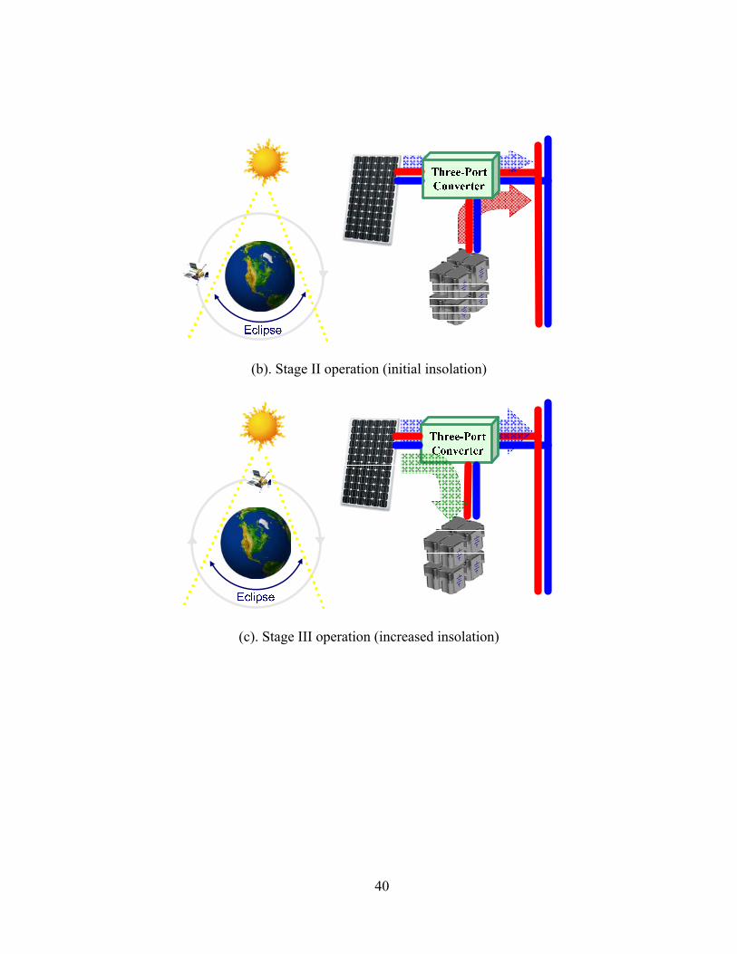
40
(b). Stage II operation (initial insolation)
(c). Stage III operation (increased insolation)
41
d). Stage IV operation (battery charge control)
Fig 3. 4: Different operational modes in satellite’s one orbit cycle. Three-port converter can
achieve MPPT, battery charge control and load regulation depending on available solar power,
battery state of charge and load profile. In stage I, battery acts as the exclusive source during
eclipse period. In stage II&III, solar power is maximized to decrease battery state of discharge
in stage II for initial insolation period and then to increase battery state of charge in stage III for
increased insolation period. In stage IV, battery charge control is applied to prevent battery
over-charging and extend battery service life.
3.3.2. Control Structure
The multi-objective control architecture which aims to regulate different power ports is shown in
Figure 3.5, control loops are named as follows: input voltage regulation (IVR), output voltage
regulation (OVR), battery voltage regulation (BVR), and battery current regulation (BCR).
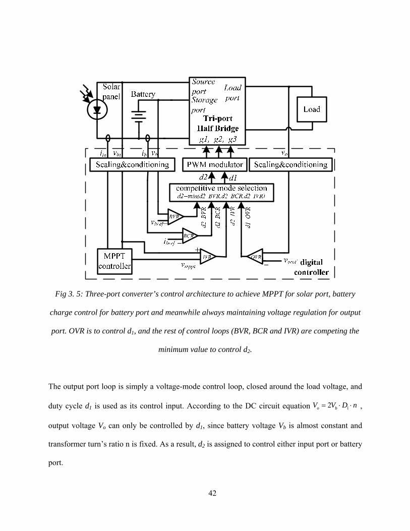
42
Fig 3. 5: Three-port converter’s control architecture to achieve MPPT for solar port, battery
charge control for battery port and meanwhile always maintaining voltage regulation for output
port. OVR is to control d1, and the rest of control loops (BVR, BCR and IVR) are competing the
minimum value to control d2.
The output port loop is simply a voltage-mode control loop, closed around the load voltage, and
duty cycle d1 is used as its control input. According to the DC circuit equation 12o bV V D n= ⋅ ⋅ ,
output voltage Vo can only be controlled by d1, since battery voltage Vb is almost constant and
transformer turn’s ratio n is fixed. As a result, d2 is assigned to control either input port or battery
port.

43
The IVR loop is used to regulate the solar panel voltage to its reference value. The reference is
provided by an MPPT controller [34] using perturb and observe algorithm, and represents an
estimate of the optimal operating voltage, duty cycle d2 is used as the control input when
realizing the IVR loop. Otherwise, d2 can be decided by battery control loop which has two
controllers, BVR and BCR. It should be mentioned that BCR is to prevent battery over-current,
so it can be considered a protection function. Under normal operation, only one of two loops
(IVR or BVR) will be active depending on the battery state of charge. Therefore, whether d2 is
commanded by IVR, BVR or BCR depends on which mode it is in.
3.3.3. Autonomous Mode Transitions
The mode of operation is determined according to the present operating conditions such as
available solar power, battery state of charge and load profile. Figure 3.6(a) gives the flow chart
for traditional mode transition algorithm. Mode 1 will be the default mode, where the converter
will spend most of the time. Mode 1 is desirable because it enables maximum solar power input.
When the converter is in Mode 1, the controller will continually check the battery parameter, and
then switch to Mode 2 if the maximum setting voltage or current is reached. Once the converter
is in Mode 2, it stays there until the load increases beyond available power. Although this
algorithm is straightforward, without careful design of mode transitions, system oscillation will
occur due to duty cycle’s instant change. In a simulation as shown in Figure 3.6(b), when battery
voltage reaches its maximum setting Vbmax, it switches to Mode 2 suddenly, that is, d2 is switched

44
from a nominal value to d2_BVR which is saturating at that moment, causing a battery voltage
spike. But when the spike of Vb reduces below Vbmax, it will force the converter to switch back to
Mode 1 and cause d2 another step change to introduce another voltage spike. And thus this
process continues for a long time. Besides, small battery voltage spike can cause huge current
spike which is usually large enough to break the circuit because of small battery internal
resistance.
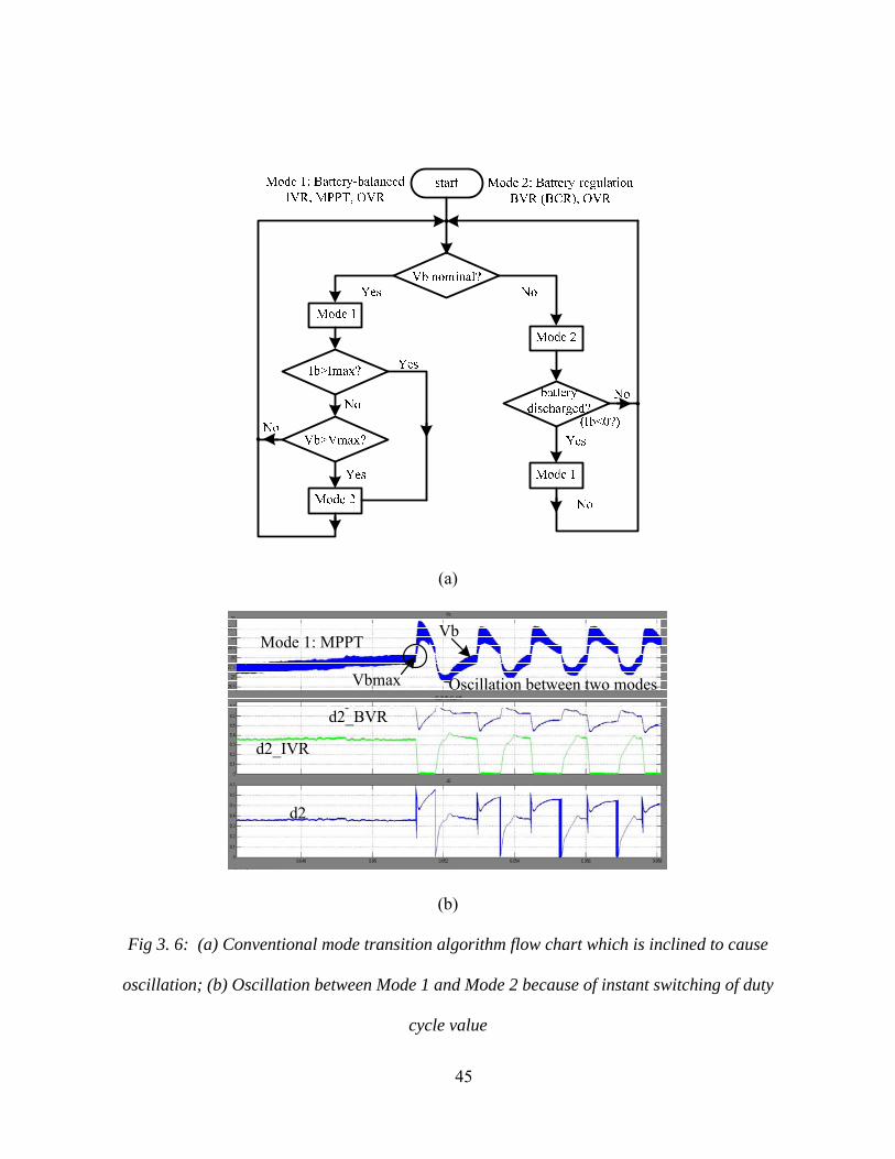
45
(a)
d2_IVR
d2_BVR
d2
Vbmax
Mode 1: MPPT
Oscillation between two modes
Vb
(b)
Fig 3. 6: (a) Conventional mode transition algorithm flow chart which is inclined to cause
oscillation; (b) Oscillation between Mode 1 and Mode 2 because of instant switching of duty
cycle value

46
In order to avoid the sudden transition between modes, the autonomous mode transition is
proposed in a competitive manor as shown in Figure 3.7(a). BVR, BCR and IVR are run in
parallel to compete for minimum value in order to win control over d2. Again, BCR will not be
active during normal operation. So battery control is mainly BVR loop operation. For example,
when converter is in Mode 1 with MPPT to maximize solar power, d2 will be determined by IVR
loop, while BVR output is saturated at its upper limit because battery voltage does not reach its
maximum setting. BVR will start to take control over d2 when battery maximum setting Vbmax is
reached and BVR output goes down to win the minimum function. It should be noted that if IVR
loop loses control, MPPT function needs to be disabled accordingly because of MPPT
algorithm’s inherent noise issue [33]. For example, in Figure 3.7(b), when converters are run in
MPPT to maximize solar power, d2 will be determined by IVR loop, while BVR output is
saturated at its upper limit because battery maximum voltage value is not reached. BVR will start
to take control when Vbmax is reached and BVR output goes down to win the minimum function.
Figure 3.7(c) shows Mode 2 to Mode 1 transition when the battery starts to discharge for sudden
increase of load demand or decrease of solar power. This method simplifies the algorithm.

47
(a)
(b)
(c)
Fig 3. 7: (a) the proposed minimum function competitive method to allow smooth transition of
modes; (b) Mode 1 to Mode 2 transition with no oscillation; (c) Mode 2 to Mode 1 transition
with no oscillation.

48
3.3.4. Converter Modeling and Controller Design
Small signal model is the basis for optimized controller design. Especially for such a
complicated MIMO system of three-port converter, an effective model will be helpful to realize
closed loop control and furthermore to optimize the converter dynamics. Since there are two
modes of operation for the three-port converter, small signal models in both modes need to be
obtained separately. Unlike conventional two-port converter, multi-port converter is high-order
system, and the symbolic derivation of these plant transfer functions is fairly tedious, so it is
difficult to obtain values of poles and zeros for analysis. Alternatively, the dynamics of the plant
can be described in a matrix form, therefore computer software is used to plot the bode graph of
different transfer functions. A common problem about MIMO system is the existence of various
interacting control loops which complicate compensator designs; therefore a decoupling network
is introduced to allow separate controller designs for each of the three power port.
3.3.4.1 Three-port Converter Modeling during Battery-Regulation Mode
Before deriving for small signal transfer functions of the converter, state equations for four
energy storage element during each circuit stage are developed. For Battery-regulation Mode,
these include the battery capacitor C1, the transformer magnetizing inductance Lm, the output
inductance Lo, and the output capacitance Co. There are three main circuit stages as illustrated in
Figure 3.8.

49
vpri
t
vb
vin-vb
iLo
t0 t1 t2 T+t0d1T d2T t
t
S2
S1 S1
t
vgs1
vgs2
S3vgs3
Fig 3. 8: Basic waveforms of the three-port converter. vpri and iLo represent transformer primary
side voltage and output inductor current, respectively.
Stage I (t0 - t1): In stage I, S1 is gated ON, applying a positive voltage to the transformer
primary side, while output inductor is charging. Synchronous Switch SR1 is gated ON to allow
current flow through output inductor Lo. Current of battery port filter capacitor is equal to the
sum of battery current, transformer magnetizing inductor current and reflected secondary side
current. The state equation in this stage is as follows.

50
11 1
1
1
/
//
/
CC Lm Lo
b
m Lm C
o Lo C o
oo o Lo
vC dv dt i n iR
L di dt vL di dt v n v
vC dv dt iR
−⎧ ⋅ = + − ⋅⎪⎪⎪ ⋅ = −⎨
⋅ = ⋅ −⎪⎪
⋅ = −⎪⎩ Eq. 3.9
Stage II (t1 - t2): In stage II, S2 is gated ON, a negative voltage is applied to the transformer
primary side, and output inductor is still charging. Synchronous Switch SR2 is gated ON to
allow a current flow path through Lo. The transformer primary voltage is input voltage subtracts
battery voltage, and thus output inductor charging rate changes accordingly. The state equation
in this stage is as follows.
11 1
2 1
2 1
/
// ( )
/
CC Lm Lo
b
m Lm C C
o Lo C C o
oo o Lo
vC dv dt i n iR
L di dt v vL di dt v v n v
vC dv dt iR
−⎧ ⋅ = + + ⋅⎪⎪⎪ ⋅ = −⎨
⋅ = − ⋅ −⎪⎪
⋅ = −⎪⎩
Eq. 3.10
Stage III (t2 - T+t0): In stage III, S3 is gated ON, zero voltage is applied to the transformer
primary side due to middle branch (S3 and D3 path)’s clamping, and output inductor is
discharging. This allows both the magnetizing and output inductor currents to free-wheel. Both
SR1 and SR2 are turned ON, therefore output inductor current distributes into both of rectifying
paths. The state equation in this stage is as follows.

51
11 1 /
/ 0/
/
CC
b
m Lm
o Lo o
oo o Lo
vC dv dtR
L di dtL di dt v
vC dv dt iR
−⎧ ⋅ =⎪⎪⎪ ⋅ =⎨
⋅ = −⎪⎪
⋅ = −⎪⎩ Eq. 3.11
Before we perform the averaging to three different state equations, we consider that the state
variables have a perturbation x̂ superimposed to the DC value X,
ˆx X x= + Eq. 3.12
And similarly, ˆd D d= + , ˆv V v= + .
To obtain the small-signal model, we assume that the perturbations are small, i.e., d̂ <<D, v̂ <<V,
etc. We also assume that the perturbations do not vary significantly during one switching period,
which means that the dynamic models that will be obtained are valid for frequencies much
smaller than the switching frequency. If we substitute Eq.3.12 in Eq.3.9, Eq.3.10, Eq.3.11, apply
the averaging to three state equations multiplied with corresponding duty cycle value, and then
neglect second order terms, we obtain small-signal equations which are demonstrated as follows.

52
( ) ( ) ( ) ( )
( )( )
( )
( )( )
( )
2 111 1 1 2 2 1 1 2
1 2 2
1 1 2 21 2
1 2 2
1 1 2 21 2
ˆ ˆˆ ˆ ˆˆˆ /
ˆ ˆˆˆ ˆ/
ˆ ˆˆˆ ˆ ˆ/
ˆˆˆ /
oCLoC Lm Lm
b
in
m Lm C in
in
o Lo C o in
oo o Lo
n V d dvC dv dt i D D n i D D I d dR R
d d D VL di dt v D D d V
D D
d d n D VL di dt v n D D v d n V
D DvC dv dt iR
⋅ ⋅ −−⋅ = + ⋅ + + ⋅ ⋅ − + ⋅ + +
+ ⋅ ⋅⋅ = − ⋅ + − + ⋅
+
− ⋅ ⋅ ⋅⋅ = ⋅ ⋅ − − + + ⋅ ⋅
+
⋅ = −
$⎧⎪⎪⎪⎪⎪⎪⎨⎪⎪⎪⎪⎪⎪⎩ Eq. 3.13
Therefore the system can be represented in a matrix form using a state-space model after
converting Eq.3.13 into frequency domain. The state-space model takes the following form.
/ ,dX dt A X B U Y I X= ⋅ + ⋅ = ⋅ Eq. 3.14
Where X is a matrix containing the state variables VC1, iLm, iLo and Vo, U is a matrix containing
the control inputs d1 and d2, Y is a matrix containing the system outputs, I is the identity matrix.
For this model the four state variables are also the system outputs. Filling in the A and B matrices
using the state equations gives the following result.
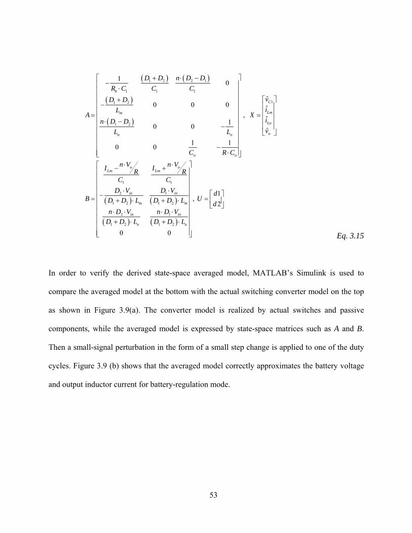
53
( ) ( )
( )
( )
( ) ( )
( )
1 2 2 1
1 1 1
11 2
1 2
1 1
2 1
1 2 1 2
2 1
1 2 1
1 0
ˆ0 0 0 ˆ
, ˆ10 0 ˆ
1 10 0
b
C
Lmm
Lo
oo o
o o
o oLm Lm
in in
m m
in in
o
D D n D DR C C C
vD DiL
A Xin D DvL L
C R C
n V n VI IR RC C
D V D VB D D L D D L
n D V n D VD D L D D
⎡ + ⋅ − ⎤−⎢ ⎥⋅⎢ ⎥
⎢ ⎥+ ⎡ ⎤−⎢ ⎥ ⎢ ⎥
⎢ ⎥ ⎢ ⎥= =⎢ ⎥ ⎢ ⎥⋅ −⎢ ⎥− ⎢ ⎥⎢ ⎥ ⎣ ⎦⎢ ⎥⎢ ⎥−⎢ ⎥⋅⎣ ⎦
⋅ ⋅− +
⋅ ⋅−= + ⋅ + ⋅
⋅ ⋅ ⋅ ⋅+ ⋅ +( )2
1,
2
0 0o
dU
d
L
⎡ ⎤⎢ ⎥⎢ ⎥⎢ ⎥⎢ ⎥ ⎡ ⎤
=⎢ ⎥ ⎢ ⎥⎣ ⎦⎢ ⎥
⎢ ⎥⎢ ⎥⋅⎢ ⎥⎢ ⎥⎣ ⎦ Eq. 3.15
In order to verify the derived state-space averaged model, MATLAB’s Simulink is used to
compare the averaged model at the bottom with the actual switching converter model on the top
as shown in Figure 3.9(a). The converter model is realized by actual switches and passive
components, while the averaged model is expressed by state-space matrices such as A and B.
Then a small-signal perturbation in the form of a small step change is applied to one of the duty
cycles. Figure 3.9 (b) shows that the averaged model correctly approximates the battery voltage
and output inductor current for battery-regulation mode.
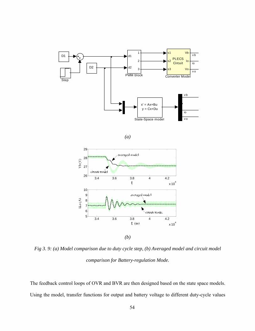
54
Step
x' = Ax+Bu y = Cx+Du
State-Space model
d1
d2
1
2
3
PWM block
s1
s2
s3
Vb
Io
Vo
PLECSCircuit
Converter Model
D2
D1
v b
v o
v b
v o
io
io
(a)
3.4 3.6 3.8 4 4.2
x 104
26
27
28
29
t
3.4 3.6 3.8 4 4.2
x 104
56789
10
t
(b)
Fig 3. 9: (a) Model comparison due to duty cycle step, (b) Averaged model and circuit model
comparison for Battery-regulation Mode.
The feedback control loops of OVR and BVR are then designed based on the state space models.
Using the model, transfer functions for output and battery voltage to different duty-cycle values
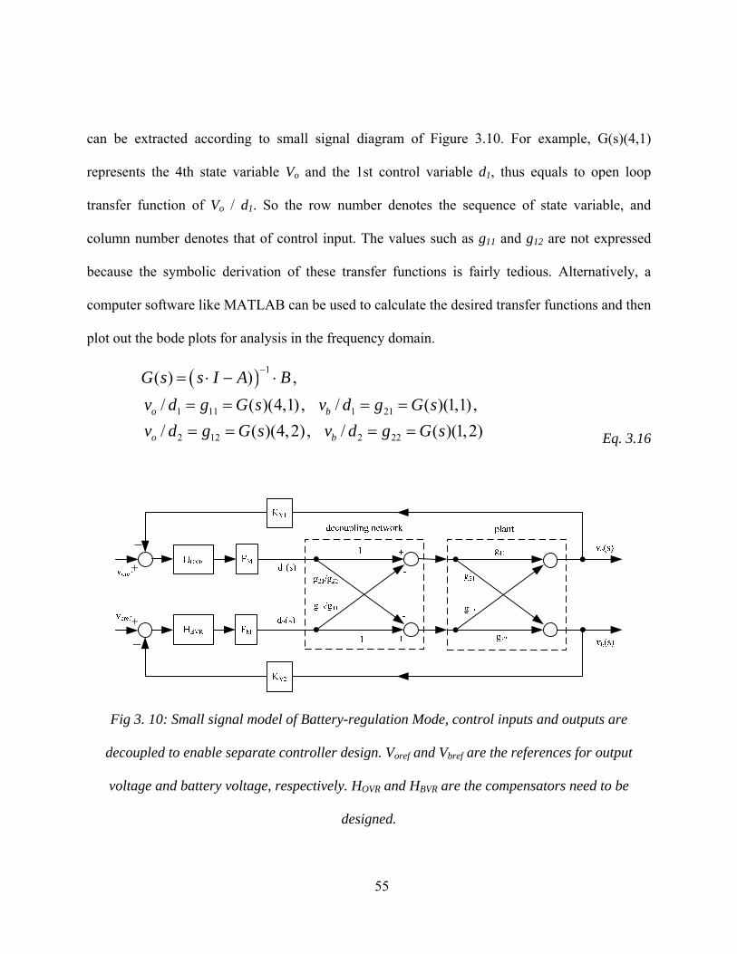
55
can be extracted according to small signal diagram of Figure 3.10. For example, G(s)(4,1)
represents the 4th state variable Vo and the 1st control variable d1, thus equals to open loop
transfer function of Vo / d1. So the row number denotes the sequence of state variable, and
column number denotes that of control input. The values such as g11 and g12 are not expressed
because the symbolic derivation of these transfer functions is fairly tedious. Alternatively, a
computer software like MATLAB can be used to calculate the desired transfer functions and then
plot out the bode plots for analysis in the frequency domain.
( ) 1
1 11 1 21
2 12 2 22
( ) ) ,/ ( )(4,1), / ( )(1,1),/ ( )(4,2), / ( )(1,2)
o b
o b
G s s I A Bv d g G s v d g G sv d g G s v d g G s
−= ⋅ − ⋅
= = = =
= = = = Eq. 3.16
−
−
+
+
Fig 3. 10: Small signal model of Battery-regulation Mode, control inputs and outputs are
decoupled to enable separate controller design. Voref and Vbref are the references for output
voltage and battery voltage, respectively. HOVR and HBVR are the compensators need to be
designed.

56
In Figure 3.10, PWM modulator gain FM is calculated using the following equation,
2 /MM s PWMclockF f f= ⋅ Eq. 3.17
Where PWMclock is the clock frequency of PWM counter, fs is the switching frequency, and M
is chosen to allow the logical value in the compare register of the PWM to be between 0 and 1.
The gains KV1 and KV2 actually take into account both sensing gain and Analog to Digital
conversion gain, the latter is dependent on the resolution of Analog to Digital converter.
As mentioned earlier, it is difficult to design close loop compensators for each control loop
without proper decoupling method. Therefore a decoupling network as in Figure 8 is introduced
so that the control loops can be designed independently with different bandwidth requirement.
Since output port voltage regulation requirement is the most stringent of the three and battery
characteristics are relatively slower, the BVR loop is designed to have a one decade lower
bandwidth than that of OVR. The derivation of decoupling network G∗ is described as follows.
The state vector matrix X can be written as X G U ∗= ⋅ , where U ∗ is the modified input vector
made up of duty cycles U, U G U∗ ∗= ⋅ . Therefore, X G G U∗= ⋅ ⋅ . According to modern control
theory, our goal is to make G G∗⋅ a diagonal matrix to allow one control input to determine one
output independently. So based on 1 1G X U G∗ − −= ⋅ ⋅ , G∗ can be derived and simplified as
12 11
21 22
1 // 1
g gG
g g∗ −⎡ ⎤= ⎢ ⎥−⎣ ⎦ Eq. 3.18
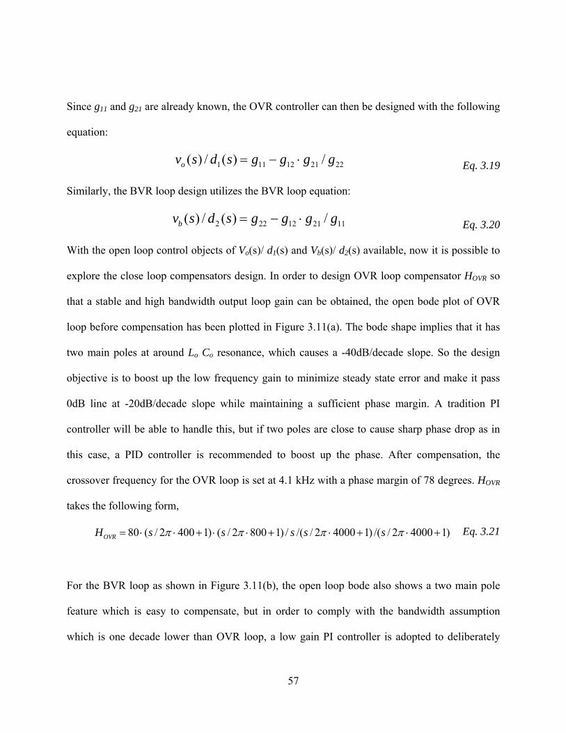
57
Since g11 and g21 are already known, the OVR controller can then be designed with the following
equation:
1 11 12 21 22( ) / ( ) /ov s d s g g g g= − ⋅ Eq. 3.19
Similarly, the BVR loop design utilizes the BVR loop equation:
2 22 12 21 11( ) / ( ) /bv s d s g g g g= − ⋅ Eq. 3.20
With the open loop control objects of Vo(s)/ d1(s) and Vb(s)/ d2(s) available, now it is possible to
explore the close loop compensators design. In order to design OVR loop compensator HOVR so
that a stable and high bandwidth output loop gain can be obtained, the open bode plot of OVR
loop before compensation has been plotted in Figure 3.11(a). The bode shape implies that it has
two main poles at around Lo Co resonance, which causes a -40dB/decade slope. So the design
objective is to boost up the low frequency gain to minimize steady state error and make it pass
0dB line at -20dB/decade slope while maintaining a sufficient phase margin. A tradition PI
controller will be able to handle this, but if two poles are close to cause sharp phase drop as in
this case, a PID controller is recommended to boost up the phase. After compensation, the
crossover frequency for the OVR loop is set at 4.1 kHz with a phase margin of 78 degrees. HOVR
takes the following form,
80 ( / 2 400 1) ( / 2 800 1) / /( / 2 4000 1) /( / 2 4000 1)OVRH s s s s sπ π π π= ⋅ ⋅ + ⋅ ⋅ + ⋅ + ⋅ + Eq. 3.21
For the BVR loop as shown in Figure 3.11(b), the open loop bode also shows a two main pole
feature which is easy to compensate, but in order to comply with the bandwidth assumption
which is one decade lower than OVR loop, a low gain PI controller is adopted to deliberately
58
shape it to cross 0dB line at the desired frequency range, and the pole will be placed in front of
zero to force a sharp drop of gain curve, but it should be noted that phase margin should be
sufficiently large to allow this kind of zero pole placement. If one set of zero and pole is not
enough, two sets of zero and pole (PID controller) may be utilized. The crossover frequency of
the BVR loop is set at 390 Hz, and phase margin of BVR is set at 88 degrees. The compensator
of HBVR used is as follows,
0.7 ( / 2 1000 1) ( / 2 1000 1) / /( / 2 200 1) /( / 2 300 1)BVRH s s s s sπ π π π= ⋅ ⋅ + ⋅ ⋅ + ⋅ + ⋅ + Eq. 3.22
102 103 104-20
0
20
40
frequency (Hz)
mag
nitu
de (d
B)
Vo to d1 bode plots (open/close loop)
102 103 104-200
-100
0
frequency (Hz)
phas
e (d
egre
e)
before compensationafter compensation
101 102 103-20
0
20
40
frequency (Hz)
mag
nitu
de (d
B)
Vb to d2 bode plots (open/close loop)
101 102 103-200
-100
0
frequency (Hz)
phas
e (d
egre
e)
before compensationafter compensation
(a) (b)
Fig 3. 11: Simulated bode plots for Battery-regulation Mode, (a) Vo(s)/ d1(s); (b) Vb(s)/ d2(s).
Dashed line denotes open loop plant transfer function before applying the compensator, solid
line denotes close loop transfer function after applying the compensator. BVR loop bandwidth is
set to be one tenth of that of OVR.

59
3.3.4.2 Three-port Converter Modeling during Battery-Balanced Mode
The same method is followed for battery-balanced mode. In this mode, the input port voltage VC2
is considered as a state variable instead of the battery port voltage VC1. Averaged model is
derived by state-space representation. The state matrix X contains the four state variables VC2, iLm,
iLo, and Vo, and the input matrix U remains the two control variables d1 and d2. The A and B
matrices take the following form:
2 2
2 2 2
22
2
2
1
2
1
2
1 0
ˆ0 0 0 ˆ
, ˆ10 0ˆ
1 10 0
10
1,
2
0 0
S
C
m Lm
Lo
o o o
o o
oLm
b b
m m
b b
o o
D n DR C C C
vDL i
A Xin D
L L v
C R C
n VI RCV D V
dL D LB U
dn V n D VL D L
⋅⎡ ⎤− − −⎢ ⎥⎢ ⎥
⎡ ⎤⎢ ⎥⎢ ⎥⎢ ⎥⎢ ⎥⎢ ⎥= =⎢ ⎥⎢ ⎥⋅
− ⎢ ⎥⎢ ⎥⎣ ⎦⎢ ⎥
⎢ ⎥−⎢ ⎥⋅⎣ ⎦
⎡ ⎤⋅⎛ ⎞− ⋅ +⎜ ⎟⎢ ⎥⎝ ⎠⎢ ⎥⋅⎢ ⎥− ⎡ ⎤⎢ ⎥⋅= = ⎢⎢ ⎥ ⎣⎢ ⎥⋅ ⋅ ⋅
⎢ ⎥⋅⎢ ⎥⎢ ⎥⎣ ⎦
⎥⎦ Eq. 3.23
Again, it can be seen from Figure 3.12 that the averaged model correctly approximates the input
voltage and output current according to the simulation. Since matrix A and B is derived, transfer
functions for output and input voltage to duty cycle values can be extracted from the small signal
model as shown in Figure 3.13.
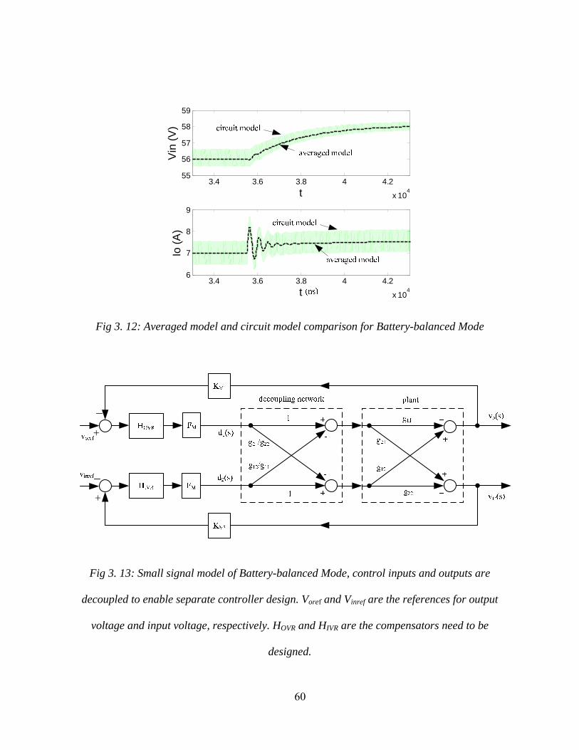
60
3.4 3.6 3.8 4 4.2
x 104
55
56
57
58
59
t
Vin
(V)
3.4 3.6 3.8 4 4.2
x 104
6
7
8
9
t
Io (A
)
Fig 3. 12: Averaged model and circuit model comparison for Battery-balanced Mode
−
−+
+
Fig 3. 13: Small signal model of Battery-balanced Mode, control inputs and outputs are
decoupled to enable separate controller design. Voref and Vinref are the references for output
voltage and input voltage, respectively. HOVR and HIVR are the compensators need to be
designed.

61
The same decoupling network is adopted here as the Battery-regulation Mode. In fact, the design
of OVR is exactly the same, because no matter in which mode, the transfer function of Vo / d1
should be the same even though different approaches are applied, therefore bode plot of Vo / d1
before and after compensation in this mode should be the same as the Battery-regulation Mode.
Then according to
2 22 12 21 11( ) / ( ) /inv s d s g g g g= − ⋅ Eq. 3.24
The Vin(s)/ d2(s) bode plot before compensation is plotted in Figure 3.14, which has high
bandwidth and 100 degrees of phase margin. IVR compensator HIVR is then designed to enforce
relatively low control loop bandwidth with some phase drop. Therefore a PI controller with
extremely low gain and one set of zero and pole is adopted to achieve this design goal. The
bandwidth of IVR loop is designed at 500 Hz, which is about one decade lower than OVR
bandwidth. The phase margin is set at 61 degrees in this case.
0.08 ( / 2 10 1) / /( / 2 200 1)IVRH s s sπ π= ⋅ ⋅ + ⋅ + Eq. 3.25
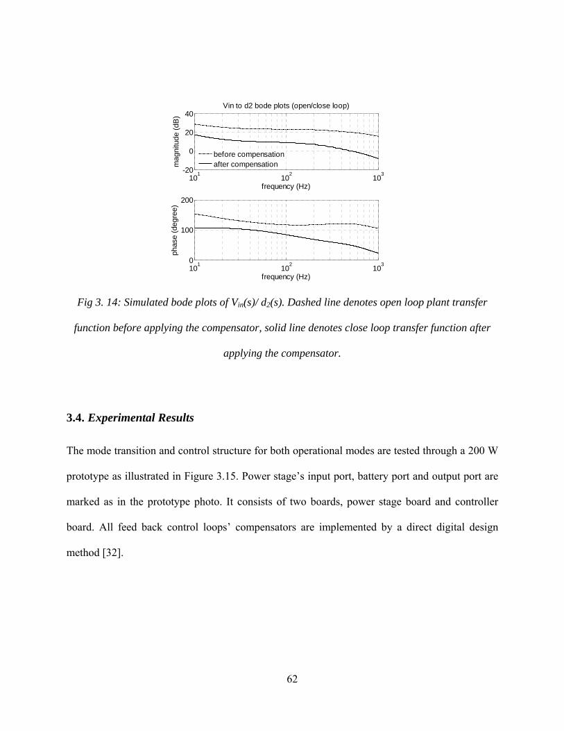
62
101 102 103-20
0
20
40
frequency (Hz)m
agni
tude
(dB
)
Vin to d2 bode plots (open/close loop)
101 102 1030
100
200
frequency (Hz)
phas
e (d
egre
e)
before compensationafter compensation
Fig 3. 14: Simulated bode plots of Vin(s)/ d2(s). Dashed line denotes open loop plant transfer
function before applying the compensator, solid line denotes close loop transfer function after
applying the compensator.
3.4. Experimental Results
The mode transition and control structure for both operational modes are tested through a 200 W
prototype as illustrated in Figure 3.15. Power stage’s input port, battery port and output port are
marked as in the prototype photo. It consists of two boards, power stage board and controller
board. All feed back control loops’ compensators are implemented by a direct digital design
method [32].
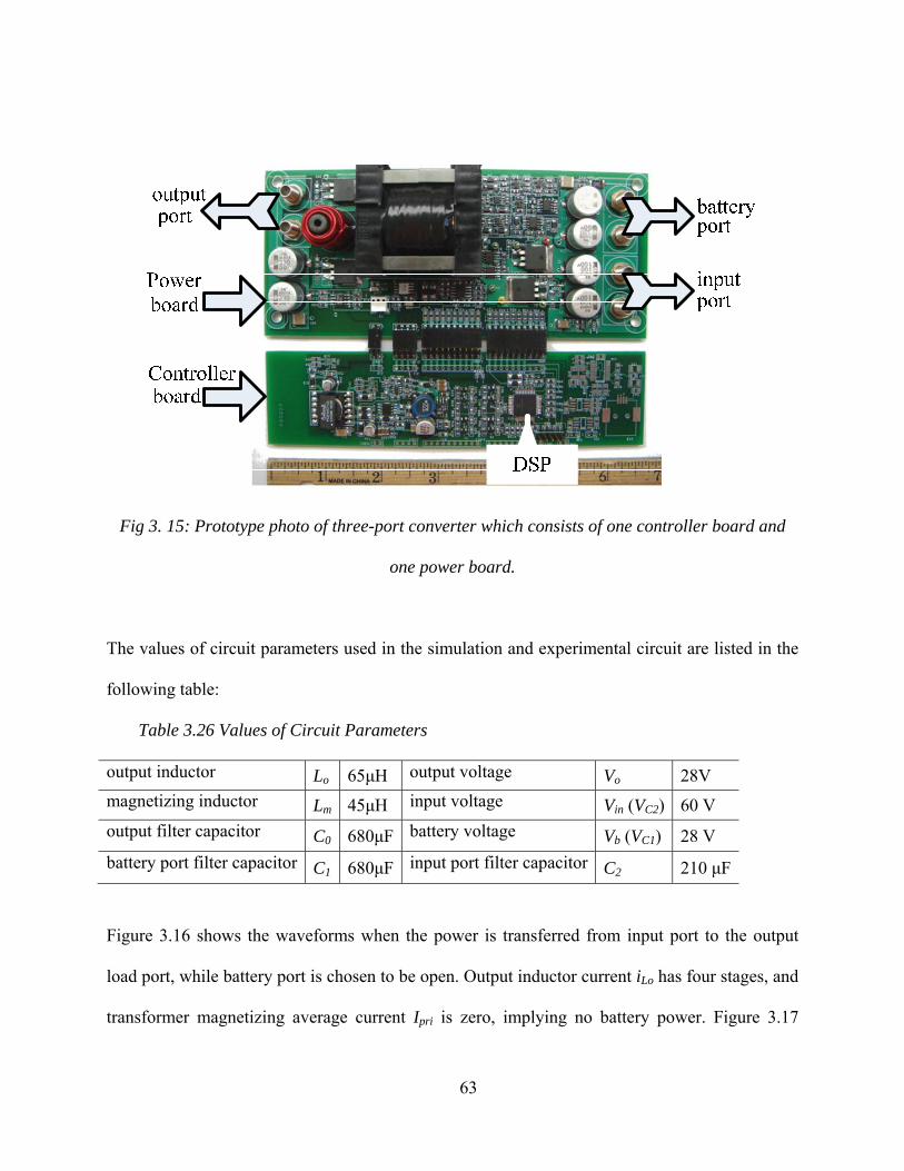
63
Fig 3. 15: Prototype photo of three-port converter which consists of one controller board and
one power board.
The values of circuit parameters used in the simulation and experimental circuit are listed in the
following table:
Table 3.26 Values of Circuit Parameters
output inductor Lo 65μH output voltage Vo 28V magnetizing inductor Lm 45μH input voltage Vin (VC2) 60 V output filter capacitor C0 680μF battery voltage Vb (VC1) 28 V battery port filter capacitor C1 680μF input port filter capacitor C2 210 μF
Figure 3.16 shows the waveforms when the power is transferred from input port to the output
load port, while battery port is chosen to be open. Output inductor current iLo has four stages, and
transformer magnetizing average current Ipri is zero, implying no battery power. Figure 3.17
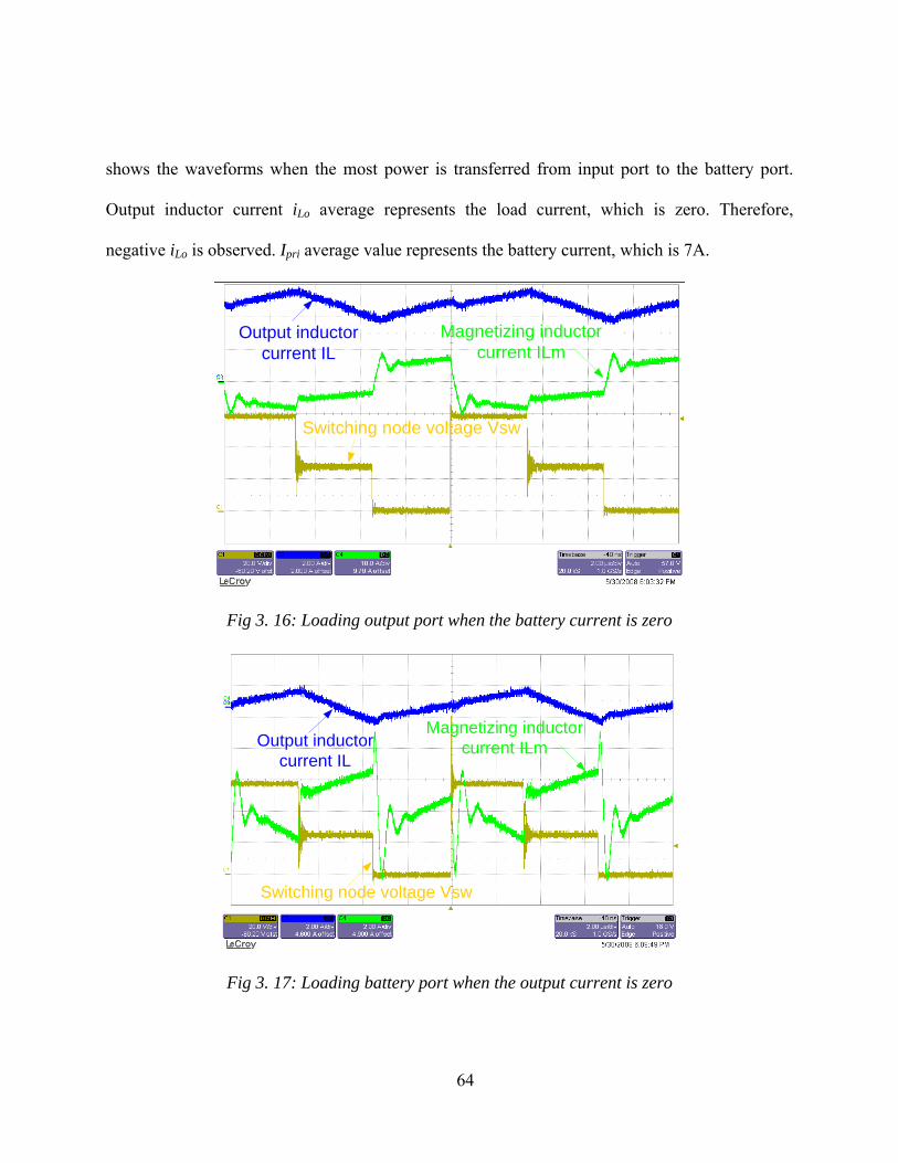
64
shows the waveforms when the most power is transferred from input port to the battery port.
Output inductor current iLo average represents the load current, which is zero. Therefore,
negative iLo is observed. Ipri average value represents the battery current, which is 7A.
Output inductor current IL
Magnetizing inductor current ILm
Switching node voltage Vsw
Fig 3. 16: Loading output port when the battery current is zero
Output inductor current IL
Magnetizing inductor current ILm
Switching node voltage Vsw
Fig 3. 17: Loading battery port when the output current is zero
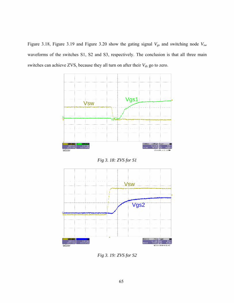
65
Figure 3.18, Figure 3.19 and Figure 3.20 show the gating signal Vgs and switching node Vsw
waveforms of the switches S1, S2 and S3, respectively. The conclusion is that all three main
switches can achieve ZVS, because they all turn on after their Vds go to zero.
Vgs1Vsw
Fig 3. 18: ZVS for S1
Vgs2
Vsw
Fig 3. 19: ZVS for S2
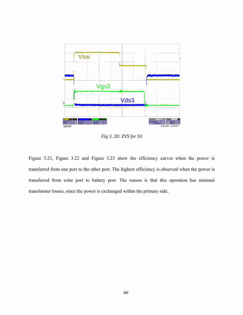
66
Vgs3
Vds3
Vsw
Fig 3. 20: ZVS for S3
Figure 3.21, Figure 3.22 and Figure 3.23 show the efficiency curves when the power is
transferred from one port to the other port. The highest efficiency is observed when the power is
transferred from solar port to battery port. The reason is that this operation has minimal
transformer losses, since the power is exchanged within the primary side.
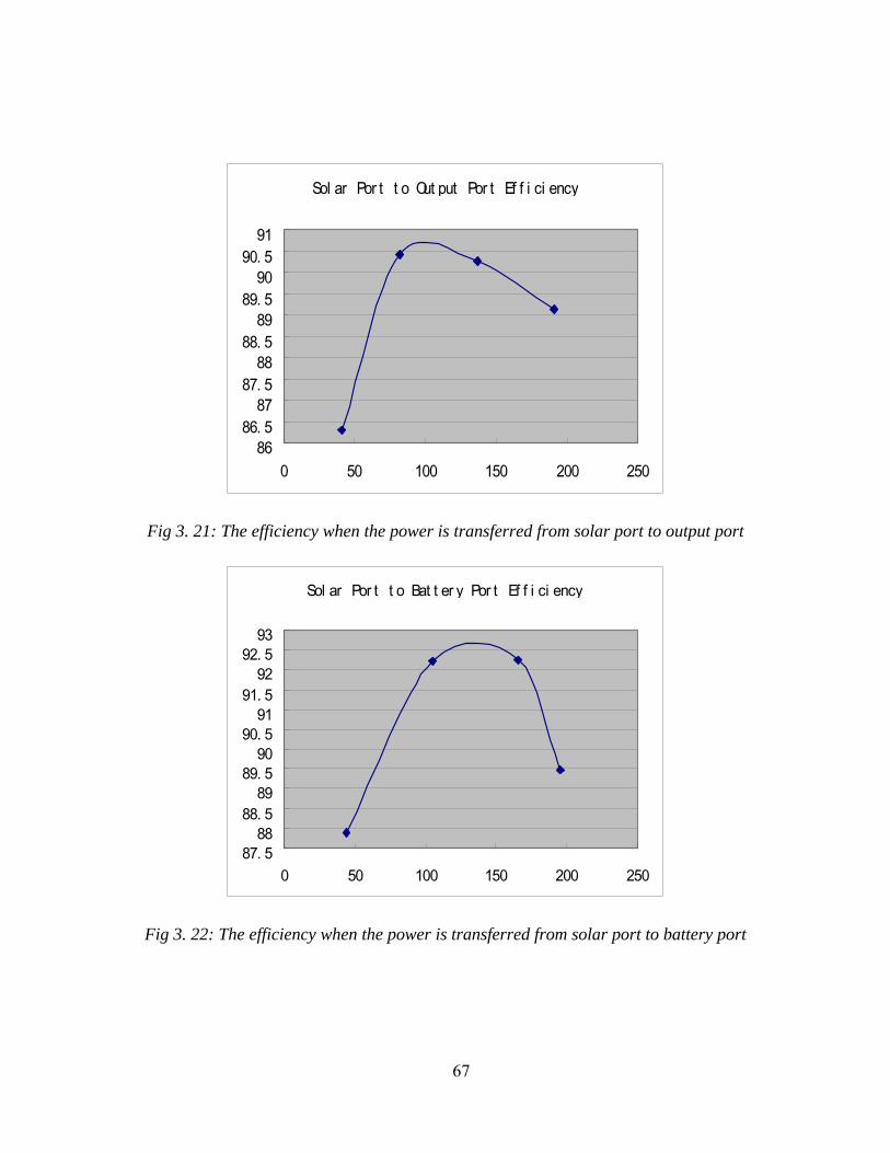
67
Sol ar Por t t o Out put Por t Ef f i ci ency
8686. 5
8787. 5
8888. 5
8989. 5
9090. 5
91
0 50 100 150 200 250
Fig 3. 21: The efficiency when the power is transferred from solar port to output port
Sol ar Por t t o Bat t er y Por t Ef f i ci ency
87. 588
88. 589
89. 590
90. 591
91. 592
92. 593
0 50 100 150 200 250
Fig 3. 22: The efficiency when the power is transferred from solar port to battery port
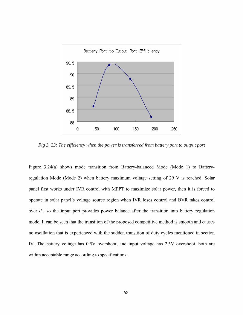
68
Bat t er y Por t t o Out put Por t Ef f i ci ency
88
88. 5
89
89. 5
90
90. 5
0 50 100 150 200 250
Fig 3. 23: The efficiency when the power is transferred from battery port to output port
Figure 3.24(a) shows mode transition from Battery-balanced Mode (Mode 1) to Battery-
regulation Mode (Mode 2) when battery maximum voltage setting of 29 V is reached. Solar
panel first works under IVR control with MPPT to maximize solar power, then it is forced to
operate in solar panel’s voltage source region when IVR loses control and BVR takes control
over d2, so the input port provides power balance after the transition into battery regulation
mode. It can be seen that the transition of the proposed competitive method is smooth and causes
no oscillation that is experienced with the sudden transition of duty cycles mentioned in section
IV. The battery voltage has 0.5V overshoot, and input voltage has 2.5V overshoot, both are
within acceptable range according to specifications.

69
Figure 3.24(b) gives Mode 2 to Mode 1 transition when load level suddenly increases to force
the battery to source instead of sink. Since battery voltage setting can not be met during
discharging, d1 will be controlled by IVR since BVR quickly loses control, and solar panel
quickly reacts to work under MPPT control so as to harvest maximum available solar power, and
battery becomes to provide the power balance in Mode 1.
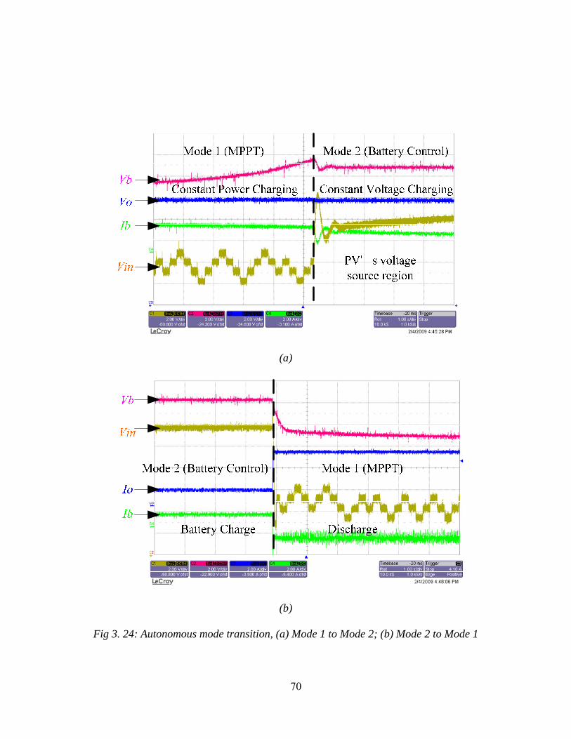
70
(a)
(b)
Fig 3. 24: Autonomous mode transition, (a) Mode 1 to Mode 2; (b) Mode 2 to Mode 1
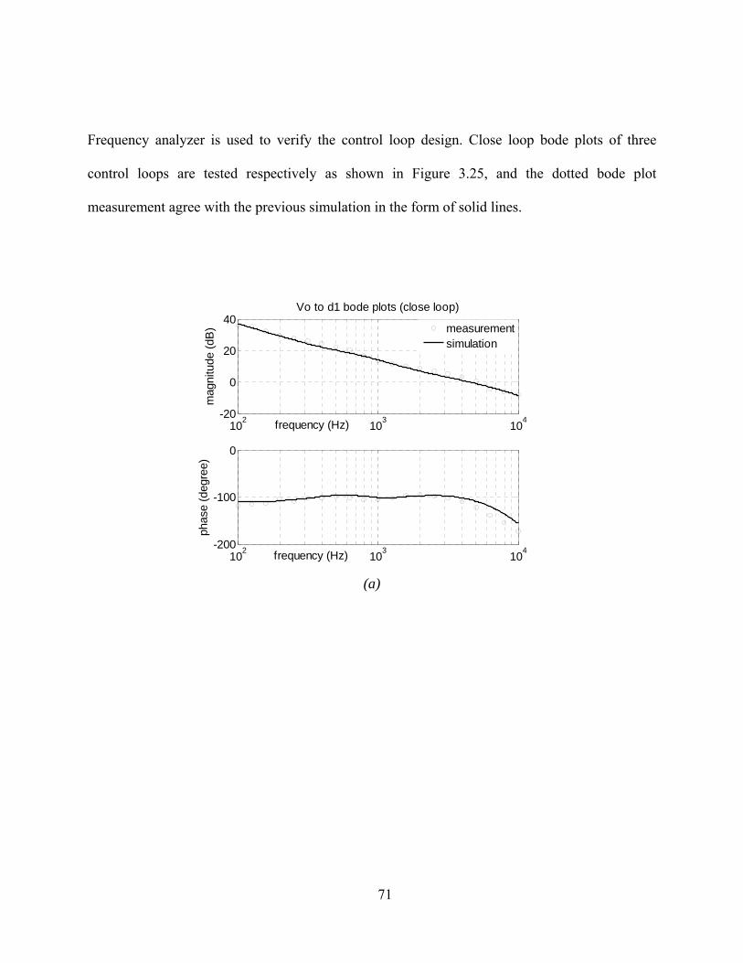
71
Frequency analyzer is used to verify the control loop design. Close loop bode plots of three
control loops are tested respectively as shown in Figure 3.25, and the dotted bode plot
measurement agree with the previous simulation in the form of solid lines.
102 103 104-20
0
20
40
frequency (Hz)
mag
nitu
de (d
B)
Vo to d1 bode plots (close loop)
102 103 104-200
-100
0
frequency (Hz)
phas
e (d
egre
e)
measurementsimulation
(a)
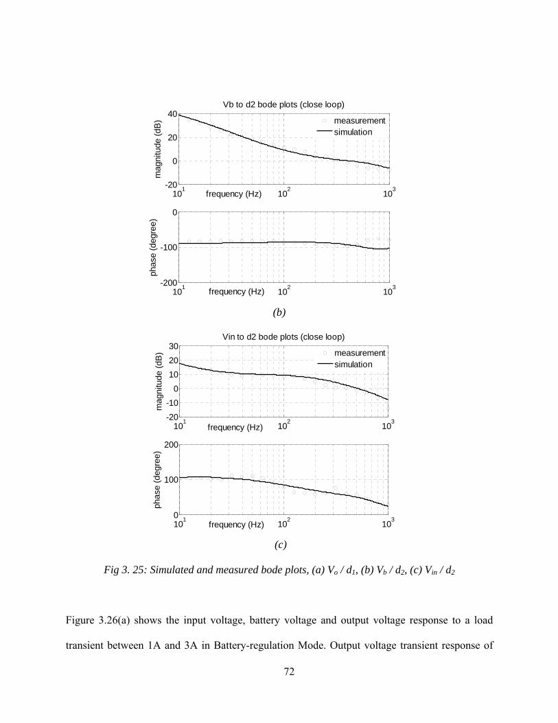
72
101 102 103-20
0
20
40
frequency (Hz)
mag
nitu
de (d
B)
Vb to d2 bode plots (close loop)
101 102 103-200
-100
0
frequency (Hz)
phas
e (d
egre
e)
measurementsimulation
(b)
101 102 103-20-10
0102030
frequency (Hz)
mag
nitu
de (d
B)
Vin to d2 bode plots (close loop)
101 102 1030
100
200
frequency (Hz)
phas
e (d
egre
e)
measurementsimulation
(c)
Fig 3. 25: Simulated and measured bode plots, (a) Vo / d1, (b) Vb / d2, (c) Vin / d2
Figure 3.26(a) shows the input voltage, battery voltage and output voltage response to a load
transient between 1A and 3A in Battery-regulation Mode. Output voltage transient response of

73
500us settling time is much faster than battery voltage settling time of 40ms because OVR
bandwidth is ten times larger than that of BVR. Input voltage changes according to load level
changes because input port provides power balance. Figure 3.26(b) demonstrates the system
transient response in Battery-balanced Mode when MPPT is active. The load step is from 1A to
5A. Input voltage response to load transient of 20ms settling time is much slower than output
voltage settling time of 500us because IVR crossover frequency is set at one tenth of that of
OVR. Input voltage remains uninterrupted at around MPP even during load changes, which is the
unique feature of three-port converters, because MPPT and load regulation can not be achieved
simultaneously by conventional two-port converter.
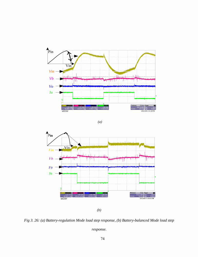
74
Vb
Vo
Vin
Io
Pin
Vin
(a)
(b)
Fig 3. 26: (a) Battery-regulation Mode load step response, (b) Battery-balanced Mode load step
response.

75
Figure 3.27 presents the typical experimental results of three different ports’ voltage and current
imitating for satellite’s one orbit cycle which includes four orbiting stages to verify the control
design for space applications. The output voltage is regulated all the time while output load level
is commanded to change from 3A to 0.5A deliberately to allow for mode transitions. As
mentioned in section II, in Stage I of satellite cycling, no solar power is available due to eclipse,
therefore input current Iin is zero and battery discharges to supply for full load. In Stage II of
initial insolation, solar panel operates in MPPT to maximize power input, but it is still not
enough to support full load, so the battery still discharges but with less discharging current, while
Iin is 1.3A. In Stage III, solar insolation level increases and solar power at this point not only
supplies for full load but also has extra to charge the battery, meanwhile battery current Ib
becomes positive. At the 30 minute point, load requirement is suddenly reduced from 3A to
0.5A. As a result, the power deficit goes to charge battery and triggers battery current regulation
to prevent over-current, so BCR takes control over d2 from previous IVR commanding, and
MPPT is disabled accordingly. During this period (30-34min), because input power and output
power is fixed, battery power is fixed as well, more specifically, battery current reduces due to
increase of battery voltage. So it eventually goes out of current protection and BCR loses control
when IVR takes control back over d2 again to operate in MPPT. Then battery voltage setting is
quickly reached, and BVR wins control over d2 and thus battery voltage is regulated, meanwhile
Ib drops gradually. When satellite enters into eclipse again, the system will go through another
same cycling period.
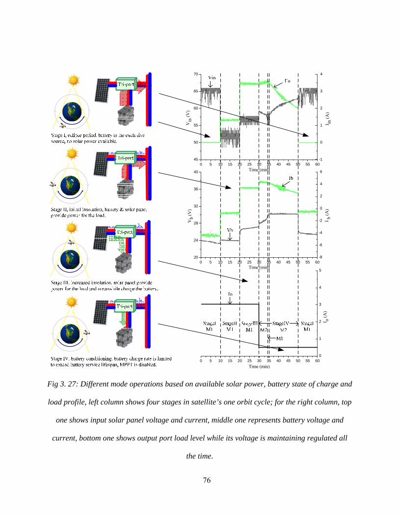
76
0 5 10 15 20 25 30 35 40 45 50 55 6045
50
55
60
65
70
-1
0
1
2
3
4
Vin
(V)
Time (min)
I in (A
)
0 5 10 15 20 25 30 35 40 45 50 55 600
1
2
3
4
5
I o (A)
Time (min)
20
24
28
32
36
40
0 5 10 15 20 25 30 35 40 45 50 55 60-8
-6
-4
-2
0
2
4
6
Vb
(V)
I b (A
)
Time (min)
Fig 3. 27: Different mode operations based on available solar power, battery state of charge and
load profile, left column shows four stages in satellite’s one orbit cycle; for the right column, top
one shows input solar panel voltage and current, middle one represents battery voltage and
current, bottom one shows output port load level while its voltage is maintaining regulated all
the time.

77
CHAPTER 4: PARALLEL OPERATION OF MULTIPLE THREE-PORT CONVERTERS
4.1. General Description
A desirable feature of a parallel system is that individual converters share the current equally and
stably. Specifically, for paralleled three-port converters, current sharing (CS) control for two of
three ports is required. In other words, traditional one port CS control is not enough for three-
port converters because unequal current distribution in the other two ports may occur due to
power stage non-identities. Moreover, how to maintain system stability while achieving good
transient CS response is a key issue since there are many interacting control loops due to power
train integration with three power ports. In this dissertation, a dual loop CS control structure is
identified to be very suitable for paralleled multi-port converters, due to the convenient
decoupling assumption between voltage loop and CS loop. A hybrid CS structure combining
both active and passive CS methods is proposed to achieve good transient CS performance
without requiring the CS bus among different converter channels.
4.2. Current Sharing for Two Paralleled Converters
A large body of work has been done in the past on the paralleled converters’ CS issue [50]-[59],
but most of the researches have focused on traditional two-port converters. Since the three-port
converter is a relatively new concept and has advantages such as multiple functionalities, low
mass and high efficiency, etc; its CS issue is also worth studying. Normally the multi-port

78
converter is a high order system with multiple interacting feedback control loops. Therefore it is
already complicated to design controllers for the integrated converter with abundance of control
loops, and the additional two CS control loops for the paralleled three-port converters will
further challenge the steady state and dynamic performance, therefore proper decoupling
between CS loop and voltage loop is necessary to prevent control loop interaction and the
dynamic analysis is desired to help judge overall system stability.
As shown in Figure 4.1, the integrated system contains two paralleled three-port converters, in
which two of three ports will be controlled simultaneously with CS control, and the two ports
being regulated simultaneously can be either the output port with the battery port, or the output
port with the input port.
bus loadTri-port
converter
controller
Fig.4. 1: Paralleled three-port converter system interfacing solar panel, battery pack and bus.
4.2.1. Output Port Current Sharing for Two Paralleled Converters
As in Figure 4.2, the proposed active CS method achieves uniform current distribution with tight
voltage regulation. More specifically, democratic (also referred to as autonomous) maximum
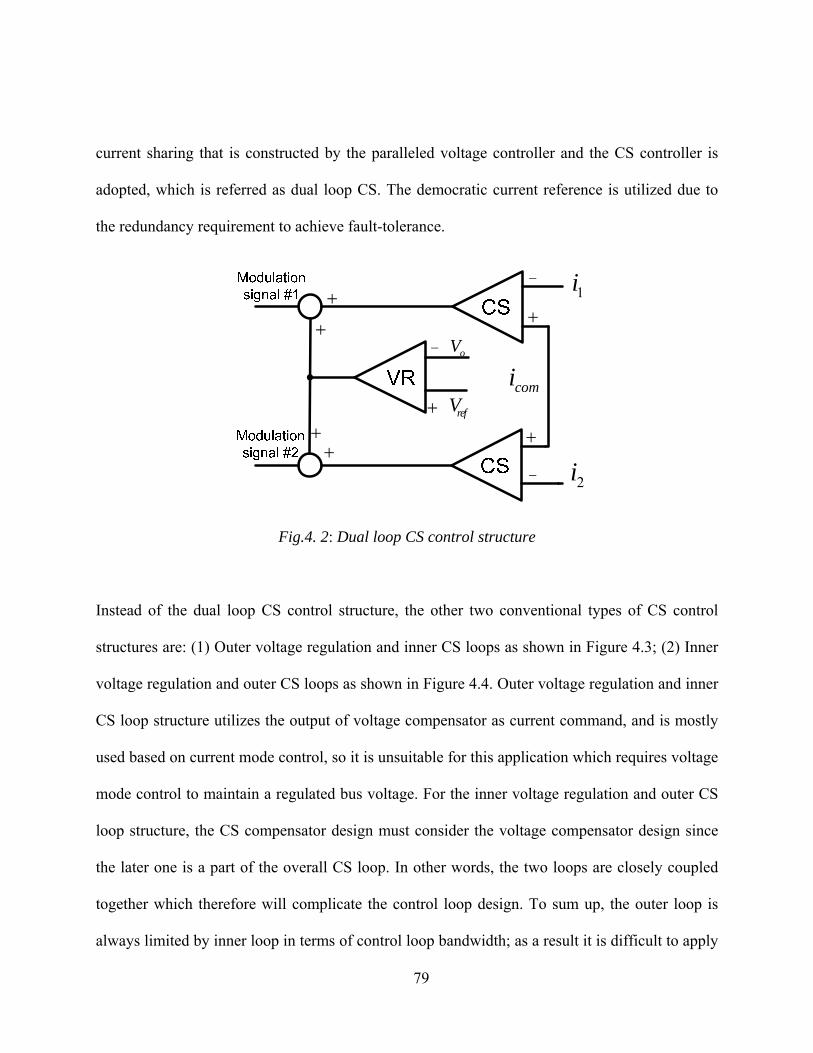
79
current sharing that is constructed by the paralleled voltage controller and the CS controller is
adopted, which is referred as dual loop CS. The democratic current reference is utilized due to
the redundancy requirement to achieve fault-tolerance.
2i
1i
comi+
+
++
+
+
−
−
refV
oV+
−
Fig.4. 2: Dual loop CS control structure
Instead of the dual loop CS control structure, the other two conventional types of CS control
structures are: (1) Outer voltage regulation and inner CS loops as shown in Figure 4.3; (2) Inner
voltage regulation and outer CS loops as shown in Figure 4.4. Outer voltage regulation and inner
CS loop structure utilizes the output of voltage compensator as current command, and is mostly
used based on current mode control, so it is unsuitable for this application which requires voltage
mode control to maintain a regulated bus voltage. For the inner voltage regulation and outer CS
loop structure, the CS compensator design must consider the voltage compensator design since
the later one is a part of the overall CS loop. In other words, the two loops are closely coupled
together which therefore will complicate the control loop design. To sum up, the outer loop is
always limited by inner loop in terms of control loop bandwidth; as a result it is difficult to apply
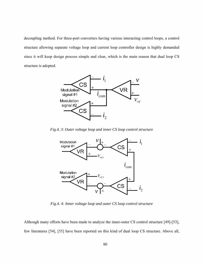
80
decoupling method. For three-port converters having various interacting control loops, a control
structure allowing separate voltage loop and current loop controller design is highly demanded
since it will keep design process simple and clear, which is the main reason that dual loop CS
structure is adopted.
++
+
−
−
−1i
2i
comirefV
v
Fig.4. 3: Outer voltage loop and inner CS loop control structure
2i
1i
comi
v
v
−
−
+
+
+
+
+
+
−
−
1refV
2refV
−
−
Fig.4. 4: Inner voltage loop and outer CS loop control structure
Although many efforts have been made to analyze the inner-outer CS control structure [49]-[53],
few literatures [54], [55] have been reported on this kind of dual loop CS structure. Above all,

81
special design considerations for three-port converters are required because of integrated power
train issue.
The advantage of paralleled CS structure is that a convenient decoupling assumption can be
made in the abundant control loops for designing such complicated systems. Small signal
analysis of the proposed paralleled CS structure shows that the CS loop and voltage loop are not
heavily coupled with each other even with large non-identities in power stages, which allows
convenient decoupling and further simplifies the compensator design.
4.2.2. Modeling of Dual-loop Current Sharing Structure
The output CS loop design of the paralleled converters with democratic maximum CS control is
composed of the following steps: 1) individual converter is designed stably with OVR closed
loop operation; 2) CS control loop is added and overall output control loop analysis is applied to
ensure overall output port stability. It should be mentioned that democratic CS and dedicated
master CS basically produce the same small signal model. Therefore without loss of generality,
module#1 is designated as master and thus module #2 is assigned as a slaver for simplicity.
Figure 4.5 gives the small signal block diagram for output control loops (VR and CS) together
with the decoupled converter model obtained in Chapter 3. HVR denotes voltage loop
compensator while HCS denotes CS loop compensator which needs to be designed.

82
When two paralleled modules are considered, voltage loop gain with CS control loops open
(outputs of both CS loops are zero) can be obtained as follows:
1 2/ ( )v y x VR vd vdT v v H G G= = ⋅ + Eq. 4.1
Obviously, for the master module, CS loop does not affect its duty cycle because CS loop output
is saturated at its lower limit, which is zero. On the other hand, CS loop output will affect duty
cycle of slaver module since it is not zero, and when considering voltage loop to be open, its CS
loop gain can be expressed as:
2i CS idT H G= ⋅ Eq. 4.2
Ti represents CS loop gain which determines CS dynamic performance and can help to derive the
overall output loop gain Tsys as follows:
1 2 2/ ( ) /(1 )sys y x v VR id id CS vd iT v v T H G G H G T= = + ⋅ − ⋅ ⋅ + Eq. 4.3
Equation (5) demonstrates when two modules are identical, that is to say, Gid1= Gid2, it only
needs to judge OVR loop itself and CS loop has no effect on overall output port stability. In
other words, the voltage loop and CS loop are 100% decoupled. However, in practice, there are
always some power stage non-identities such as component tolerances and temperature
variations and connection asymmetry among converters; otherwise, CS can be achieved naturally
since converters are exactly the same and are connected symmetrically. Since Gid1 will not be
exactly the same as Gid2, the question now becomes how Tsys will be different with Tv if some

83
values of power stage parameters are not the same. Since the converter model derived only
includes those passive component values (without considering active components like
MOSFETs), 30% deviation of output filter inductor L and output filter capacitor C values (both
including equivalent series resistances) are assumed. Therefore, to consider the worst case
scenario, module #2 is assumed to have 70% L and C values of those of module #1. Then bode
plots are calculated and plotted through computer software MATLAB to show the deviation
between voltage loop gain Tv and overall system loop gain Tsys. CS loop gain Ti is designed to
have high bandwidth (1kHz compared with 3kHz for voltage loop) with sufficient phase margins
to achieve good CS dynamic response during load transients.
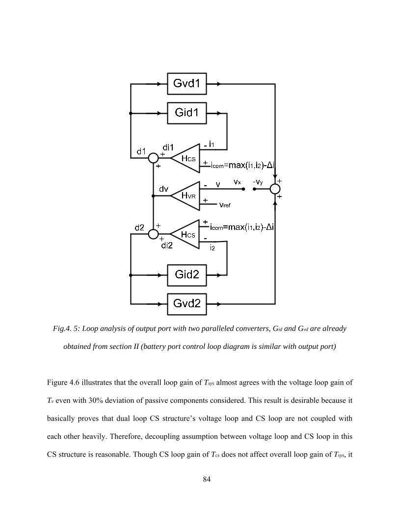
84
Fig.4. 5: Loop analysis of output port with two paralleled converters, Gid and Gvd are already
obtained from section II (battery port control loop diagram is similar with output port)
Figure 4.6 illustrates that the overall loop gain of Tsys almost agrees with the voltage loop gain of
Tv even with 30% deviation of passive components considered. This result is desirable because it
basically proves that dual loop CS structure’s voltage loop and CS loop are not coupled with
each other heavily. Therefore, decoupling assumption between voltage loop and CS loop in this
CS structure is reasonable. Though CS loop gain of Tcs does not affect overall loop gain of Tsys, it
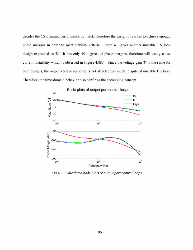
85
decides the CS dynamic performance by itself. Therefore the design of Tcs has to achieve enough
phase margins in order to meet stability criteria. Figure 4.7 gives another unstable CS loop
design expressed as Tcs’, it has only 10 degrees of phase margins, therefore will easily cause
current instability which is observed in Figure 4.8(b). Since the voltage gain Tv is the same for
both designs, the output voltage response is not affected too much in spite of unstable CS loop.
Therefore, the time-domain behavior also confirms the decoupling concept.
102
103
104
-40
-20
0
20
40
Mag
nitu
de (d
B)
Bode plots of output port control loops
102 103 104-200
-150
-100
-50
frequency (Hz)
Pha
se M
argi
n (d
eg)
TvTiTsys
Fig.4. 6: Calculated bode plots of output port control loops
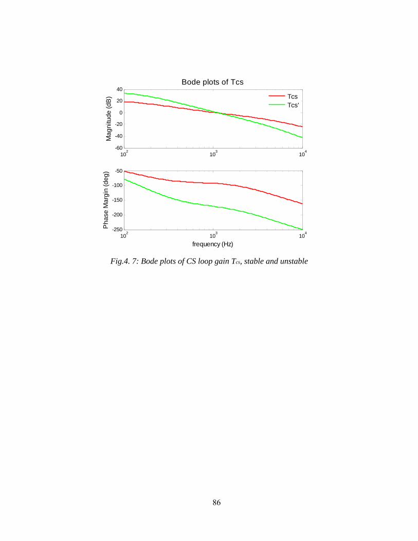
86
102
103
104
-60
-40
-20
0
20
40
Mag
nitu
de (d
B)
Bode plots of Tcs
102
103
104
-250
-200
-150
-100
-50
frequency (Hz)
Pha
se M
argi
n (d
eg)
TcsTcs'
Fig.4. 7: Bode plots of CS loop gain Tcs, stable and unstable
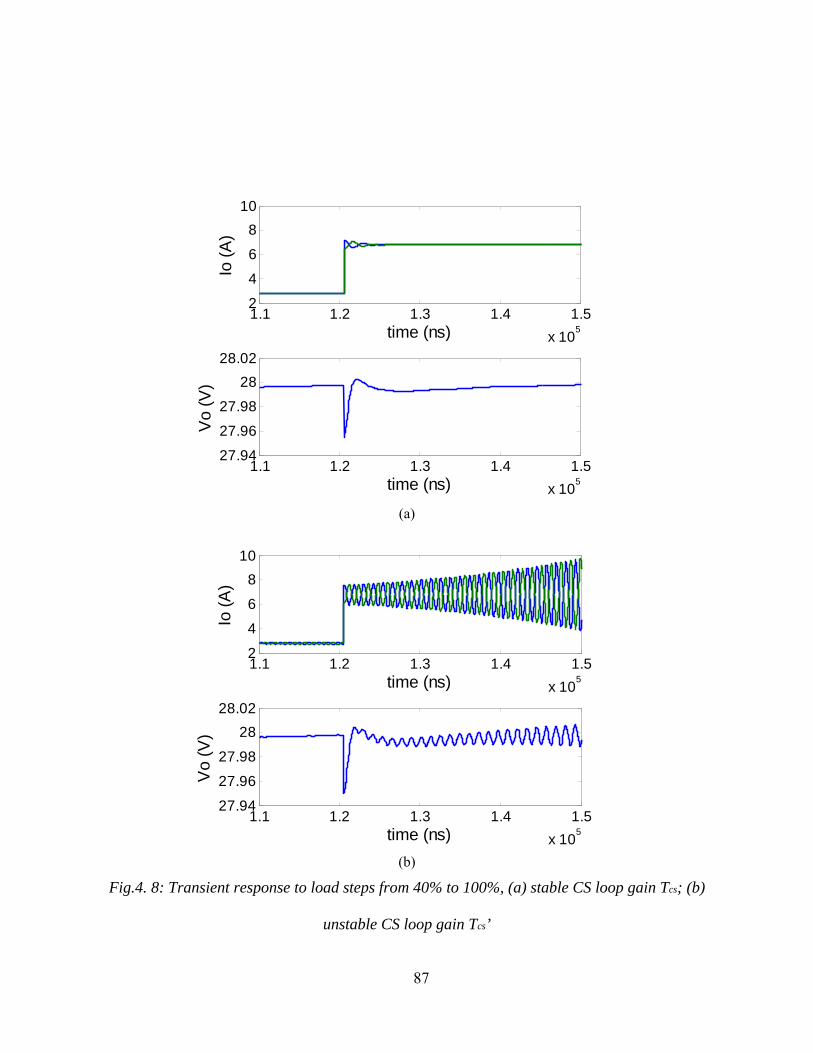
87
1.1 1.2 1.3 1.4 1.5x 10⁵
2
4
6
810
time (ns)
Io (A
)
1.1 1.2 1.3 1.4 1.5x 10⁵
27.94
27.96
27.98
2828.02
time (ns)
Vo
(V)
(a)
1.1 1.2 1.3 1.4 1.5x 10⁵
2
4
6
810
time (ns)
Io (A
)
1.1 1.2 1.3 1.4 1.5x 10⁵
27.94
27.96
27.98
2828.02
time (ns)
Vo
(V)
(b)
Fig.4. 8: Transient response to load steps from 40% to 100%, (a) stable CS loop gain Tcs; (b)
unstable CS loop gain Tcs’

88
4.2.3. Battery Port Current Sharing for Two Paralleled Converters
Two-Stage Charging delivers power to the battery in two steps as shown in Figure 4.9. In the
first step, the battery is charged by maximum available solar power which is the deficit of input
and output power, so it can be taken as a constant power charging period, in which battery
voltage rises gradually. When the battery upper voltage setting Vbmax is met, the converter will
switch to regulate its voltage to prevent over-charging, which is the second charging step. But
one thing that should be mentioned is that unlike regular constant current battery charging, the
battery cannot obtain a constant charging current because of solar power and load changes as
shown in Figure 4.10 and Figure 4.11. Figure 4.10 illustrates the MPP moves from A to C during
irradiance increase when load is constant, and the available battery energy is the difference of
input and output load power. B, C provide increased charging current for battery, while no
charging current will be available at A. Figure 4.11 shows the battery power during load changes.
A, B provide decreased charging current, while battery discharges at C.
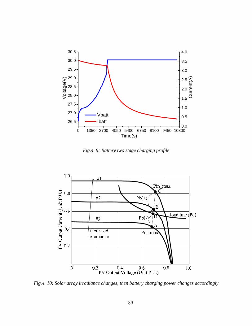
89
0 1350 2700 4050 5400 6750 8100 9450 10800
26.5
27.0
27.5
28.0
28.5
29.0
29.5
30.0
30.5
0.0
0.5
1.0
1.5
2.0
2.5
3.0
3.5
4.0
Vol
tage
(V)
Time(s)
Vbatt
Cur
rent
(A)
Ibatt
Fig.4. 9: Battery two stage charging profile
Fig.4. 10: Solar array irradiance changes, then battery charging power changes accordingly
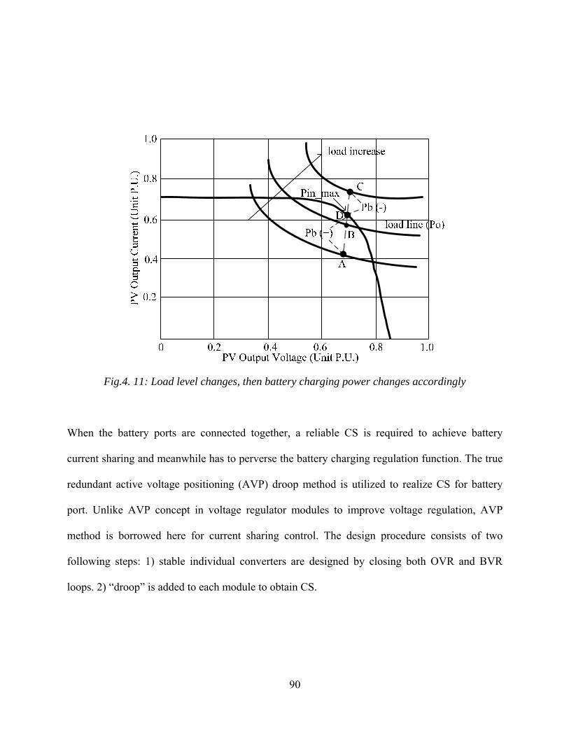
90
Fig.4. 11: Load level changes, then battery charging power changes accordingly
When the battery ports are connected together, a reliable CS is required to achieve battery
current sharing and meanwhile has to perverse the battery charging regulation function. The true
redundant active voltage positioning (AVP) droop method is utilized to realize CS for battery
port. Unlike AVP concept in voltage regulator modules to improve voltage regulation, AVP
method is borrowed here for current sharing control. The design procedure consists of two
following steps: 1) stable individual converters are designed by closing both OVR and BVR
loops. 2) “droop” is added to each module to obtain CS.
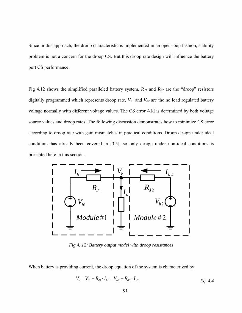
91
Since in this approach, the droop characteristic is implemented in an open-loop fashion, stability
problem is not a concern for the droop CS. But this droop rate design will influence the battery
port CS performance.
Fig 4.12 shows the simplified paralleled battery system. Rd1 and Rd2 are the “droop” resistors
digitally programmed which represents droop rate, Vb1 and Vb2 are the no load regulated battery
voltage normally with different voltage values. The CS error Δ I/I is determined by both voltage
source values and droop rates. The following discussion demonstrates how to minimize CS error
according to droop rate with gain mismatches in practical conditions. Droop design under ideal
conditions has already been covered in [3,5], so only design under non-ideal conditions is
presented here in this section.
1dR 2dR
1bV 2bV
bV
oI
#1Module # 2Module
1bI 2bI
Fig.4. 12: Battery output model with droop resistances
When battery is providing current, the droop equation of the system is characterized by:
1 1 1 2 2 2b b d b b d bV V R I V R I= − ⋅ = − ⋅ Eq. 4.4

92
The droop rate actually includes the information of CS network, ADC, and the programming
droop rate. So even though the programming droop rate is the same for both modules, different
CS error may occur due to different current sensing gain and ADC gain as shown by Figure 4.13.
Figure 4.13(a) is the undesirable condition which gives increased CS error as the load increases.
Figure 4.13(b) is acceptable since CS error remains the same value as the load increases. The
desirable droop rate setting is that we can achieve the result of Figure 4.13(c) or Figure 4.13(d).
The difference is that two modules share equal current at 50% load for (c) or 100% load for (d).
Therefore different programming droop rate is suggested to compensate different sensing gain
and ADC gain. The design rule is straightforward as indicated by Fig 9 that the one with higher
voltage reference should have a larger droop rate.
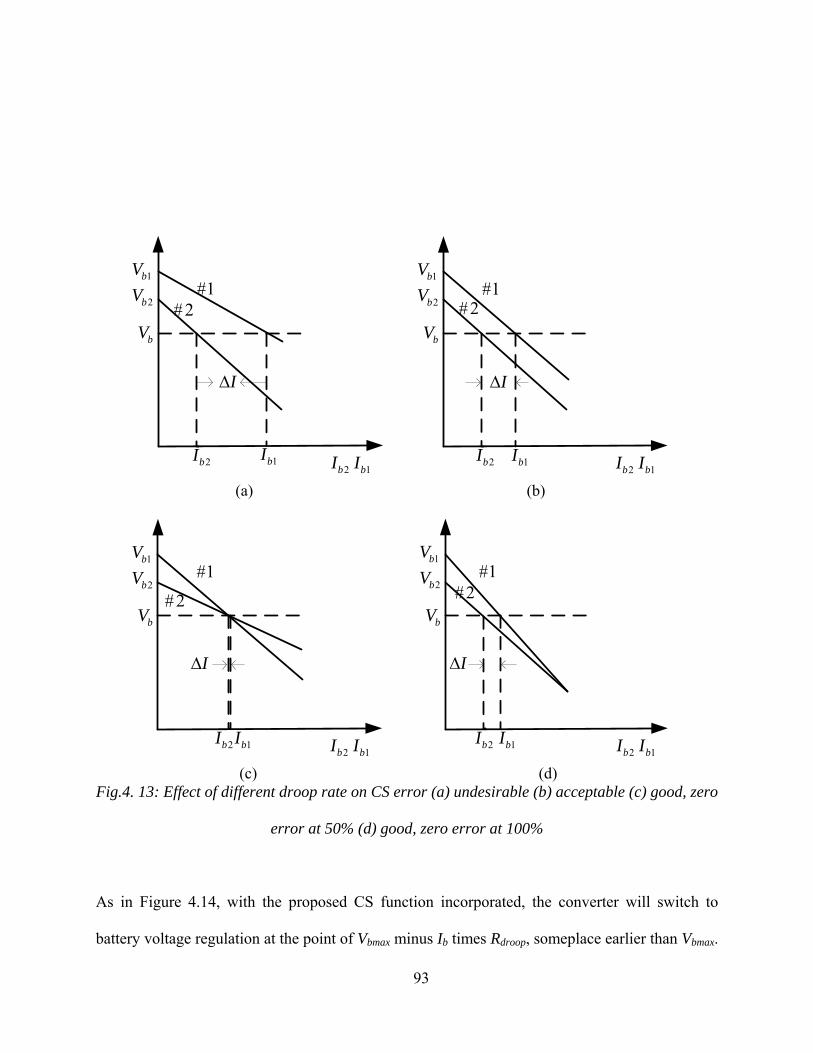
93
#1#2
1bV
2bV
bV
1bI2bI1bI2bI
IΔ
#1#2
1bV
2bV
bV
1bI2bI1bI2bI
IΔ
(a) (b)
#1
# 2
1bV
2bV
bV
1bI2bI1bI2bI
IΔ
#1#2
1bV
2bV
bV
1bI2bI1bI2bI
IΔ
(c) (d)
Fig.4. 13: Effect of different droop rate on CS error (a) undesirable (b) acceptable (c) good, zero
error at 50% (d) good, zero error at 100%
As in Figure 4.14, with the proposed CS function incorporated, the converter will switch to
battery voltage regulation at the point of Vbmax minus Ib times Rdroop, someplace earlier than Vbmax.
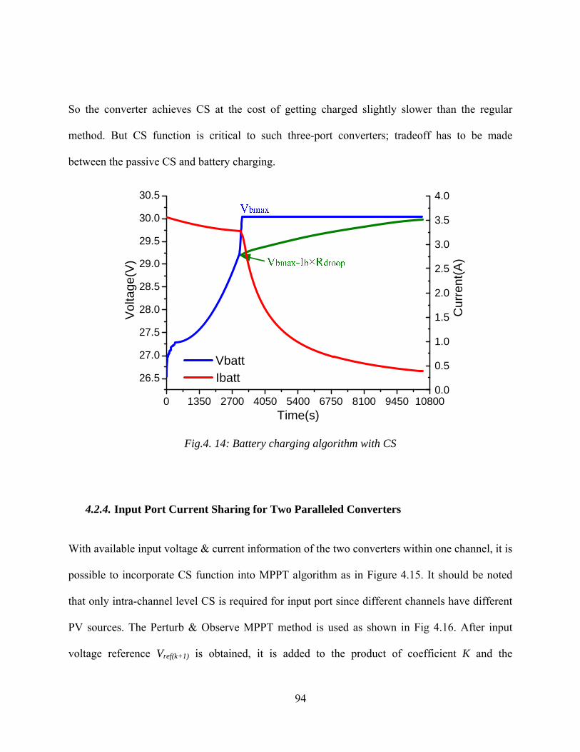
94
So the converter achieves CS at the cost of getting charged slightly slower than the regular
method. But CS function is critical to such three-port converters; tradeoff has to be made
between the passive CS and battery charging.
0 1350 2700 4050 5400 6750 8100 9450 10800
26.5
27.0
27.5
28.0
28.5
29.0
29.5
30.0
30.5
0.0
0.5
1.0
1.5
2.0
2.5
3.0
3.5
4.0
Vol
tage
(V)
Time(s)
Vbatt
Cur
rent
(A)
Ibatt
Fig.4. 14: Battery charging algorithm with CS
4.2.4. Input Port Current Sharing for Two Paralleled Converters
With available input voltage & current information of the two converters within one channel, it is
possible to incorporate CS function into MPPT algorithm as in Figure 4.15. It should be noted
that only intra-channel level CS is required for input port since different channels have different
PV sources. The Perturb & Observe MPPT method is used as shown in Fig 4.16. After input
voltage reference Vref(k+1) is obtained, it is added to the product of coefficient K and the
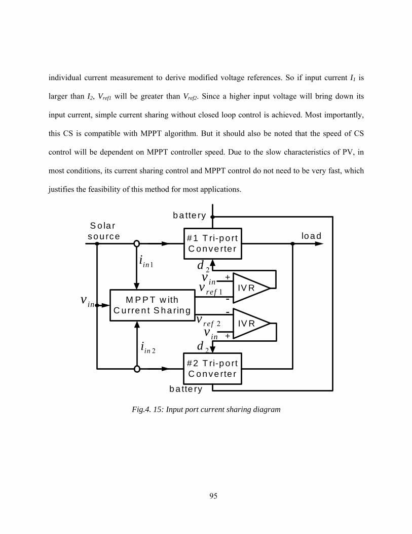
95
individual current measurement to derive modified voltage references. So if input current I1 is
larger than I2, Vref1 will be greater than Vref2. Since a higher input voltage will bring down its
input current, simple current sharing without closed loop control is achieved. Most importantly,
this CS is compatible with MPPT algorithm. But it should also be noted that the speed of CS
control will be dependent on MPPT controller speed. Due to the slow characteristics of PV, in
most conditions, its current sharing control and MPPT control do not need to be very fast, which
justifies the feasibility of this method for most applications.
# 1 T ri-po rt C on ve rte r
# 2 T ri-po rt C on ve rte r
IV R
2ini
1ini2d
loa d
ba tte ryS o la r
sou rce
2d
inv 1refv
2refvM P P T w ith
C u rren t S ha rin gIV R
inv
+
+
--
inv
ba tte ry
Fig.4. 15: Input port current sharing diagram
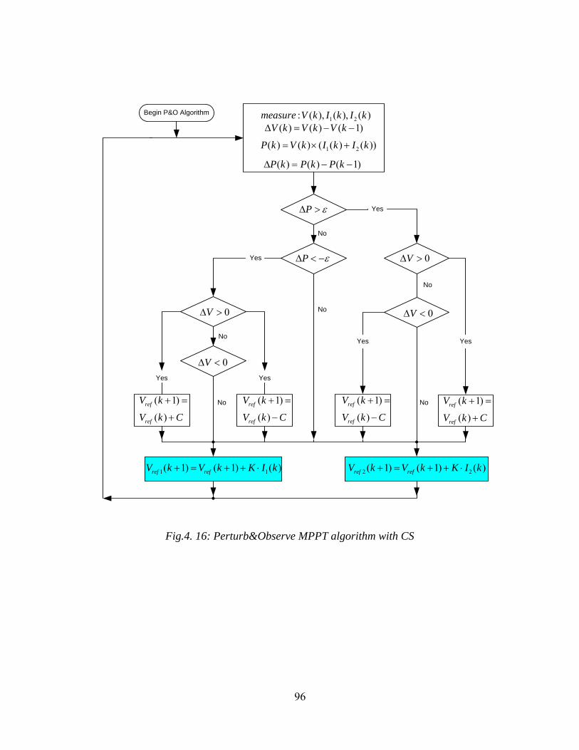
96
( ) ( ) ( 1)V k V k V kΔ = − −
1 2( ) ( ) ( ( ) ( ))P k V k I k I k= × +
( ) ( ) ( 1)P k P k P kΔ = − −
P εΔ >
P εΔ < − 0VΔ >
0VΔ <
( 1)
( )ref
ref
V k
V k C
+ =
+
( 1)
( )ref
ref
V k
V k C
+ =
−
( 1)
( )ref
ref
V k
V k C
+ =
−
( 1)
( )ref
ref
V k
V k C
+ =
+
0VΔ >
0VΔ <
1 1( 1) ( 1) ( )ref refV k V k K I k+ = + + ⋅ 2 2( 1) ( 1) ( )ref refV k V k K I k+ = + + ⋅
Yes
No
No
No
NoYes
Yes
No No
Yes
Yes
Yes
1 2: ( ), ( ), ( )measure V k I k I kBegin P&O Algorithm
Fig.4. 16: Perturb&Observe MPPT algorithm with CS
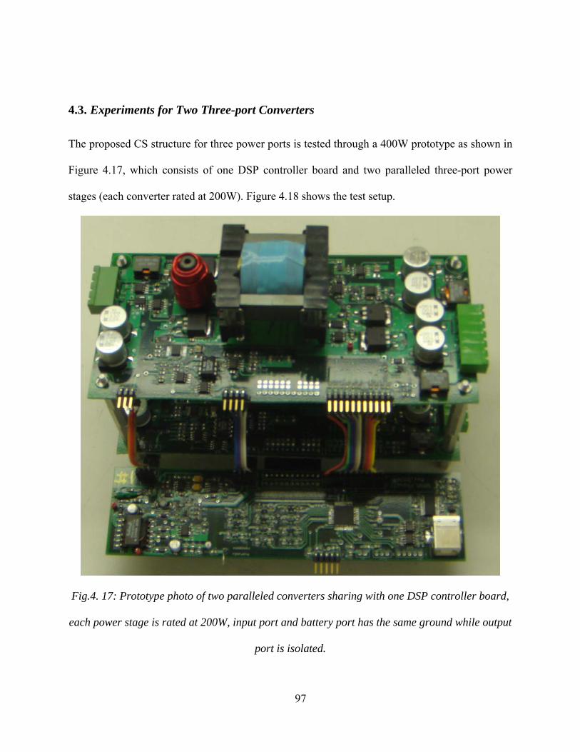
97
4.3. Experiments for Two Three-port Converters
The proposed CS structure for three power ports is tested through a 400W prototype as shown in
Figure 4.17, which consists of one DSP controller board and two paralleled three-port power
stages (each converter rated at 200W). Figure 4.18 shows the test setup.
Fig.4. 17: Prototype photo of two paralleled converters sharing with one DSP controller board,
each power stage is rated at 200W, input port and battery port has the same ground while output
port is isolated.
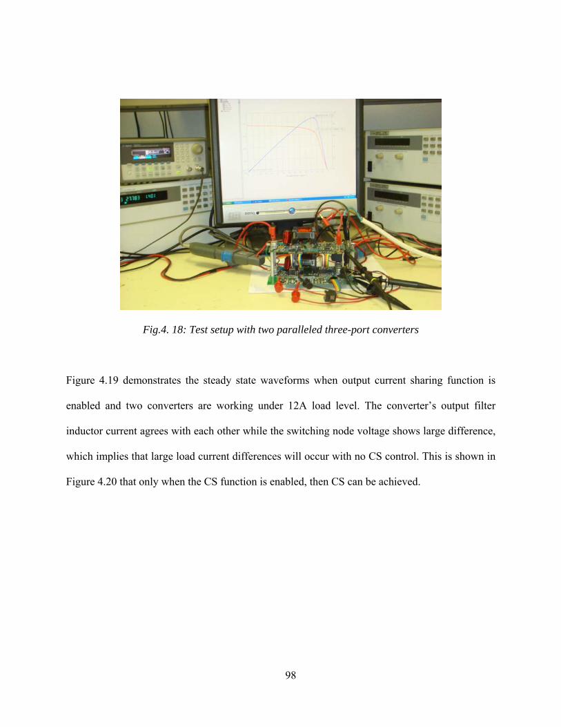
98
Fig.4. 18: Test setup with two paralleled three-port converters
Figure 4.19 demonstrates the steady state waveforms when output current sharing function is
enabled and two converters are working under 12A load level. The converter’s output filter
inductor current agrees with each other while the switching node voltage shows large difference,
which implies that large load current differences will occur with no CS control. This is shown in
Figure 4.20 that only when the CS function is enabled, then CS can be achieved.
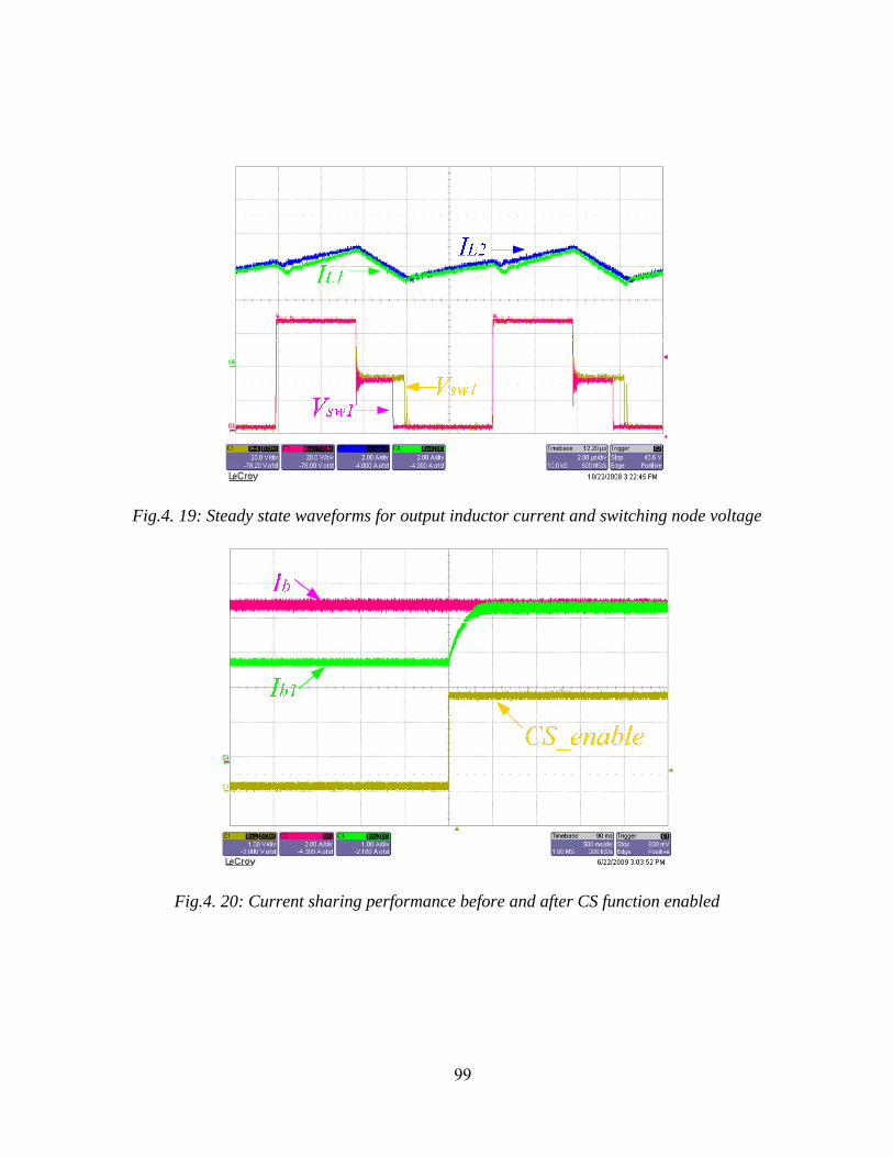
99
Fig.4. 19: Steady state waveforms for output inductor current and switching node voltage
Fig.4. 20: Current sharing performance before and after CS function enabled
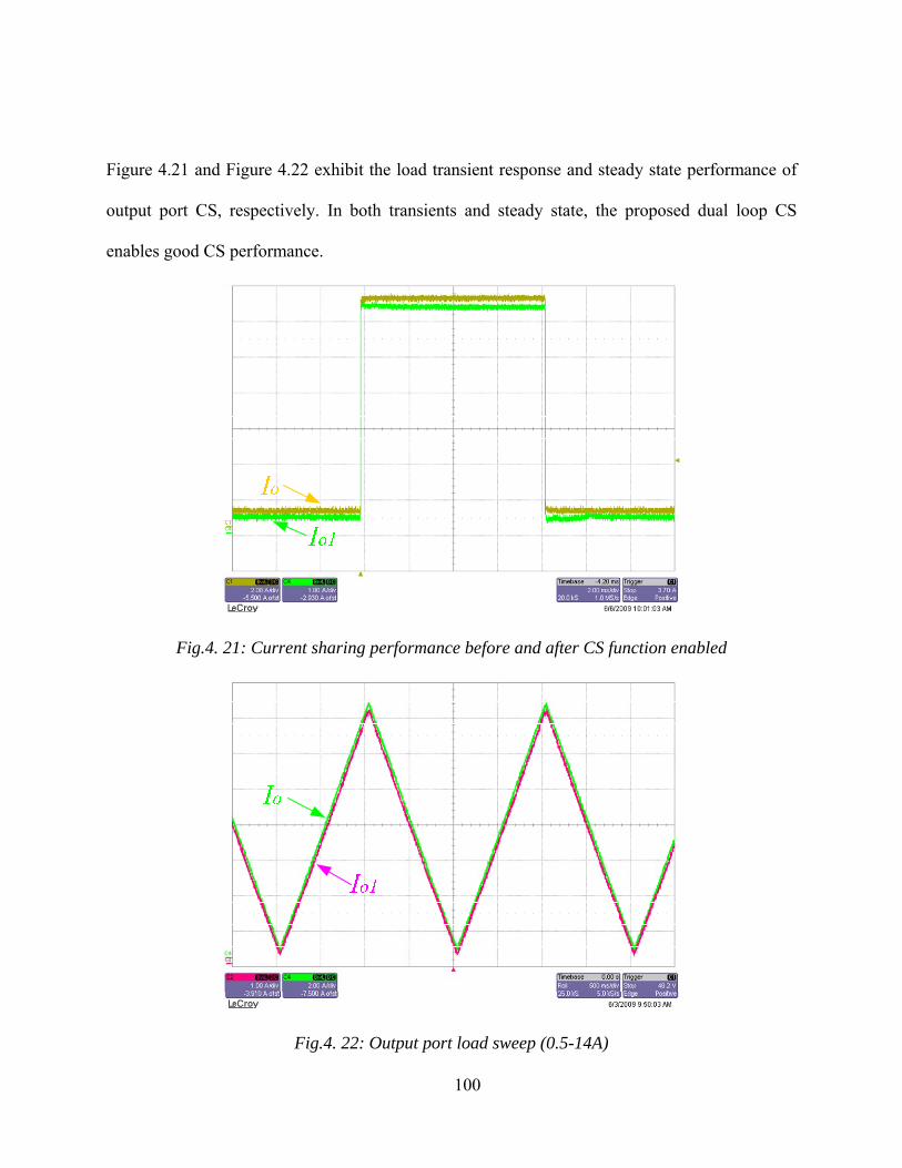
100
Figure 4.21 and Figure 4.22 exhibit the load transient response and steady state performance of
output port CS, respectively. In both transients and steady state, the proposed dual loop CS
enables good CS performance.
Fig.4. 21: Current sharing performance before and after CS function enabled
Fig.4. 22: Output port load sweep (0.5-14A)
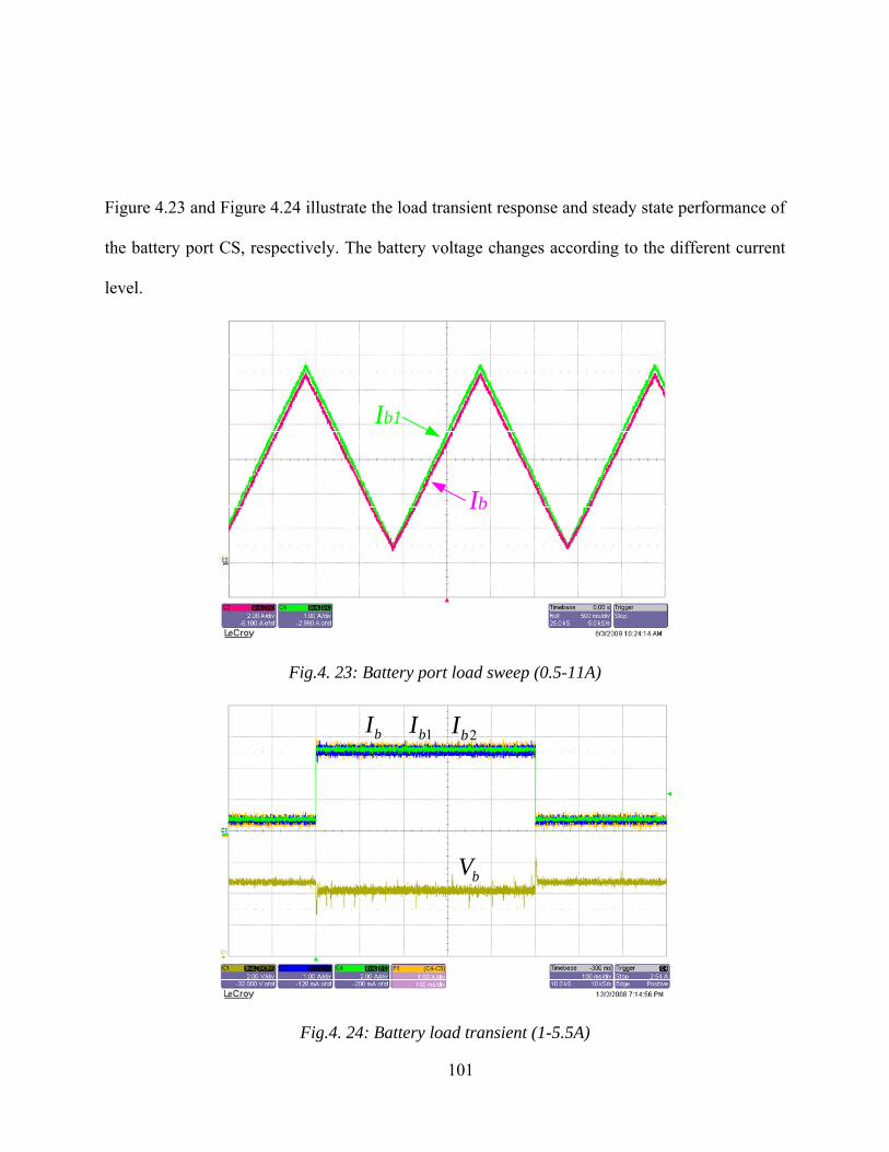
101
Figure 4.23 and Figure 4.24 illustrate the load transient response and steady state performance of
the battery port CS, respectively. The battery voltage changes according to the different current
level.
Ib1
Ib
Fig.4. 23: Battery port load sweep (0.5-11A)
bV
bI 1bI 2bI
Fig.4. 24: Battery load transient (1-5.5A)
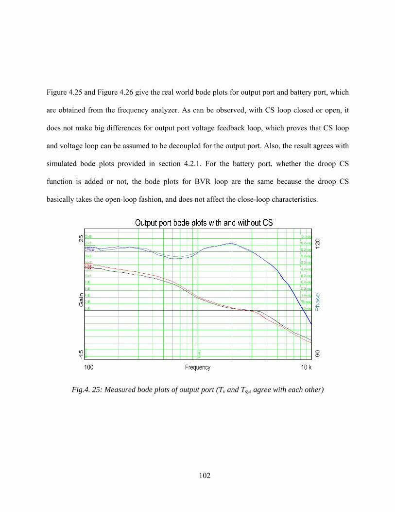
102
Figure 4.25 and Figure 4.26 give the real world bode plots for output port and battery port, which
are obtained from the frequency analyzer. As can be observed, with CS loop closed or open, it
does not make big differences for output port voltage feedback loop, which proves that CS loop
and voltage loop can be assumed to be decoupled for the output port. Also, the result agrees with
simulated bode plots provided in section 4.2.1. For the battery port, whether the droop CS
function is added or not, the bode plots for BVR loop are the same because the droop CS
basically takes the open-loop fashion, and does not affect the close-loop characteristics.
Fig.4. 25: Measured bode plots of output port (Tv and Tsys agree with each other)
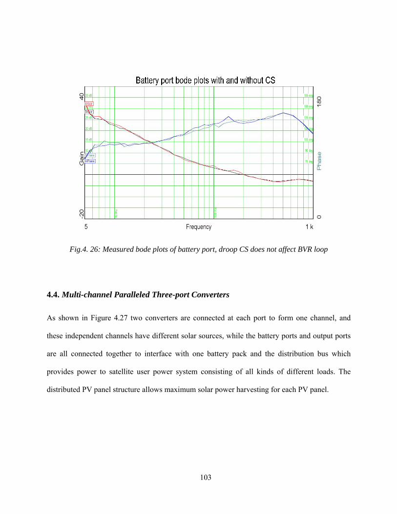
103
Fig.4. 26: Measured bode plots of battery port, droop CS does not affect BVR loop
4.4. Multi-channel Paralleled Three-port Converters
As shown in Figure 4.27 two converters are connected at each port to form one channel, and
these independent channels have different solar sources, while the battery ports and output ports
are all connected together to interface with one battery pack and the distribution bus which
provides power to satellite user power system consisting of all kinds of different loads. The
distributed PV panel structure allows maximum solar power harvesting for each PV panel.
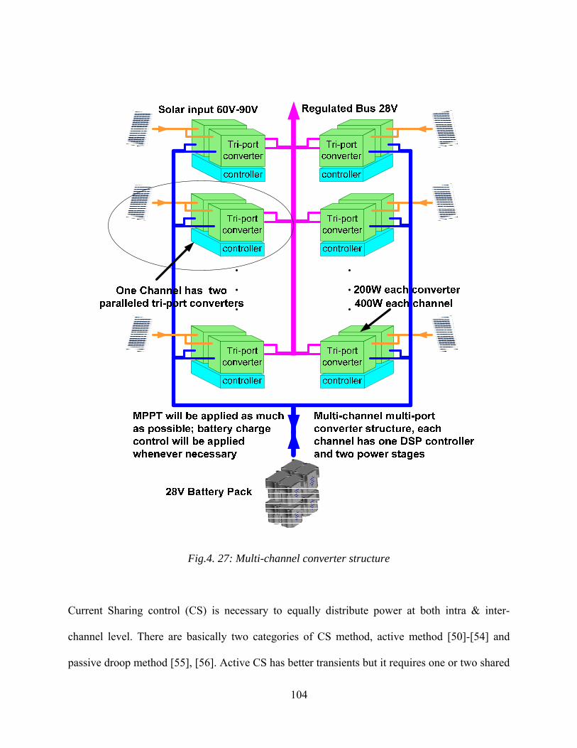
104
Fig.4. 27: Multi-channel converter structure
Current Sharing control (CS) is necessary to equally distribute power at both intra & inter-
channel level. There are basically two categories of CS method, active method [50]-[54] and
passive droop method [55], [56]. Active CS has better transients but it requires one or two shared
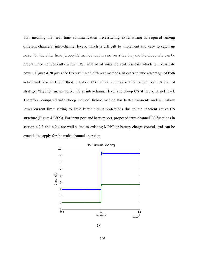
105
bus, meaning that real time communication necessitating extra wiring is required among
different channels (inter-channel level), which is difficult to implement and easy to catch up
noise. On the other hand, droop CS method requires no bus structure, and the droop rate can be
programmed conveniently within DSP instead of inserting real resistors which will dissipate
power. Figure 4.28 gives the CS result with different methods. In order to take advantage of both
active and passive CS method, a hybrid CS method is proposed for output port CS control
strategy. “Hybrid” means active CS at intra-channel level and droop CS at inter-channel level.
Therefore, compared with droop method, hybrid method has better transients and will allow
lower current limit setting to have better circuit protections due to the inherent active CS
structure (Figure 4.28(b)). For input port and battery port, proposed intra-channel CS functions in
section 4.2.3 and 4.2.4 are well suited to existing MPPT or battery charge control, and can be
extended to apply for the multi-channel operation.
0.5 1 1.5
x 104
1
2
3
4
5
6
7
8
9
10
time(us)
Cur
rent
(A)
No Current Sharing
(a)
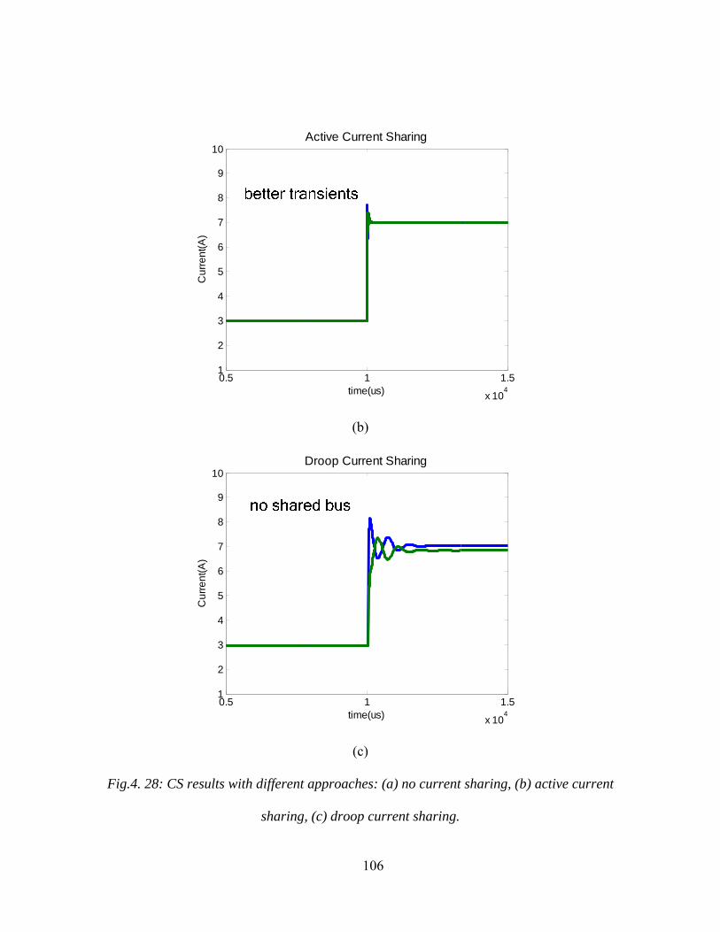
106
0.5 1 1.5
x 104
1
2
3
4
5
6
7
8
9
10
time(us)
Cur
rent
(A)
Active Current Sharing
(b)
0.5 1 1.5
x 104
1
2
3
4
5
6
7
8
9
10
time(us)
Cur
rent
(A)
Droop Current Sharing
(c)
Fig.4. 28: CS results with different approaches: (a) no current sharing, (b) active current
sharing, (c) droop current sharing.
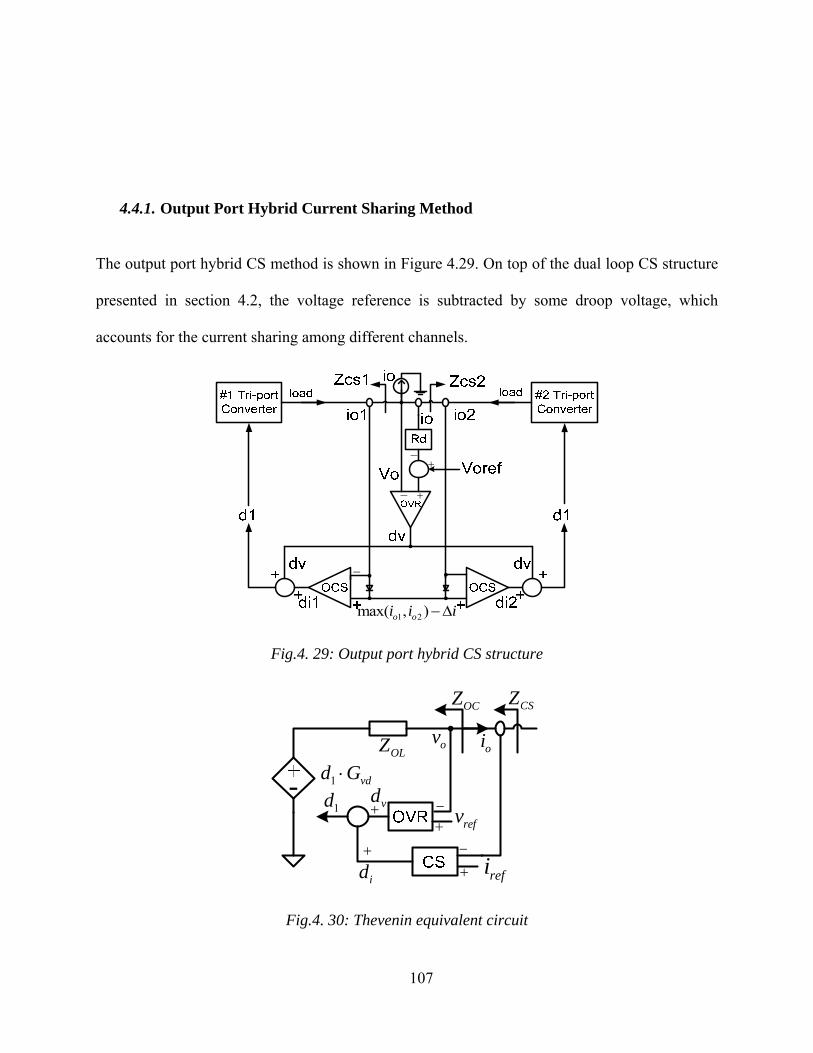
107
4.4.1. Output Port Hybrid Current Sharing Method
The output port hybrid CS method is shown in Figure 4.29. On top of the dual loop CS structure
presented in section 4.2, the voltage reference is subtracted by some droop voltage, which
accounts for the current sharing among different channels.
1 2max( , )o oi i i−Δ
−
− +
+−
Fig.4. 29: Output port hybrid CS structure
1 vdd G⋅OLZ oiov
refi+
+
+
−
−
id
vd1d
OCZ CSZ
refv+
Fig.4. 30: Thevenin equivalent circuit

108
This section introduces an effective method to judge CS performance through the thevenin
equivalent impedance, thus output impedance is to judge output CS performance. Its DC value
determines steady state CS error, and the dynamic CS performance during transients is
determined by its impedance value over the interested frequency range. To illustrate the
impedance analysis approach, the power stage is represented by a thevenin equivalent circuit in
series with an impedance as shown in Figure 4.30. We can understand ZOL, ZOC, ZCS as follows:
ZOL represents the open loop impedance without considering OVR and CS loop; ZOC represents
the close loop impedance with OVR closed but CS loop left open; ZCS represents the modified
impedance with both OVR and CS closed. In other words, we can simply treat the converter as a
black box only represented by this small signal impedance ZCS. And ZCS for each module can be
derived as follows:
11
1 1
1 2 1 22
2 1 1 2 2 1
1
(1 )
o OLCS
o OVR vd
o OL OL OL CS vdCS
o OL OVR vd CS vd OVR vd OL
v ZZi H G
v Z Z Z H GZi Z H G H G H G Z
⎧ = − =⎪ + ⋅⎪⎨ ⋅ + ⋅ ⋅⎪ = − =⎪ + + ⋅ ⋅ ⋅ + ⋅ ⋅⎩ Eq. 4.5
The expression for the admittance YCS2 which is the reciprocal of ZCS2 can be further simplified
as follows:
2 2 1( ) /(1 )CS OC OC CS CSY Y Y T T= + ⋅ ⋅ + Eq. 4.6
Where 2 2/CS CS vd OLT H G Z= ⋅ is defined as the CS loop gain.
Examination of this equation indicates that in the case of identical modules (YOC1= YOC2), the
term (1+TCS) will cancel out meaning that CS will be achieved naturally for such identical

109
modules. But unfortunately modules are not identical in reality due to their variations of
parameters. So the objective is to modify terminal impedance to make them equal to each other
in the desired frequency range. For instance, if the crossover frequency of CS loop gain TCS is
designed to be high, the impedance of different converter terminals will be altered to match each
other in that frequency range as shown in Figure 4.31. As a result, CS transients of hybrid CS
will be improved compared with conventional droop method as shown in Figure 4.32.
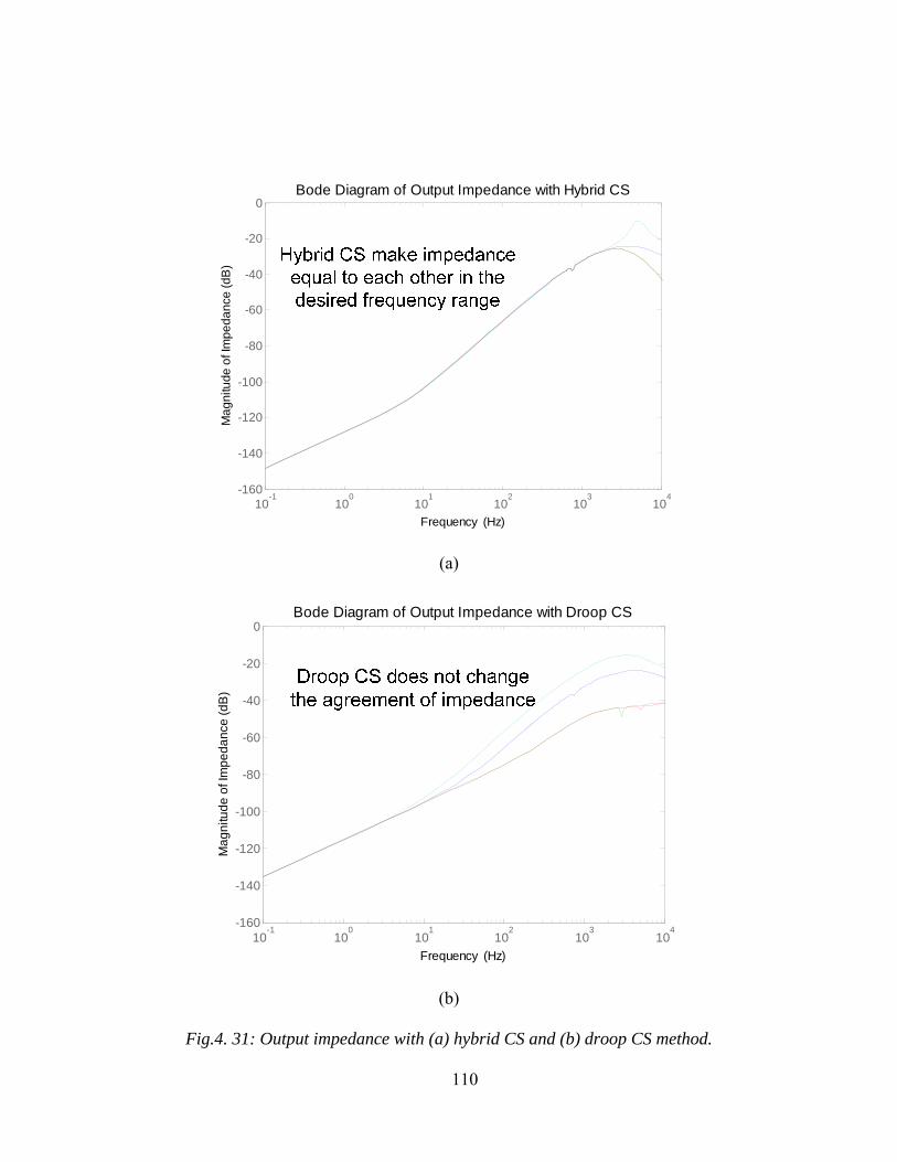
110
10-1
100
101
102
103
104
-160
-140
-120
-100
-80
-60
-40
-20
0
Mag
nitu
de o
f Im
peda
nce
(dB
)
Bode Diagram of Output Impedance with Hybrid CS
Frequency (Hz)
(a)
10-1
100
101
102
103
104
-160
-140
-120
-100
-80
-60
-40
-20
0
Mag
nitu
de o
f Im
peda
nce
(dB
)
Bode Diagram of Output Impedance with Droop CS
Frequency (Hz)
(b)
Fig.4. 31: Output impedance with (a) hybrid CS and (b) droop CS method.
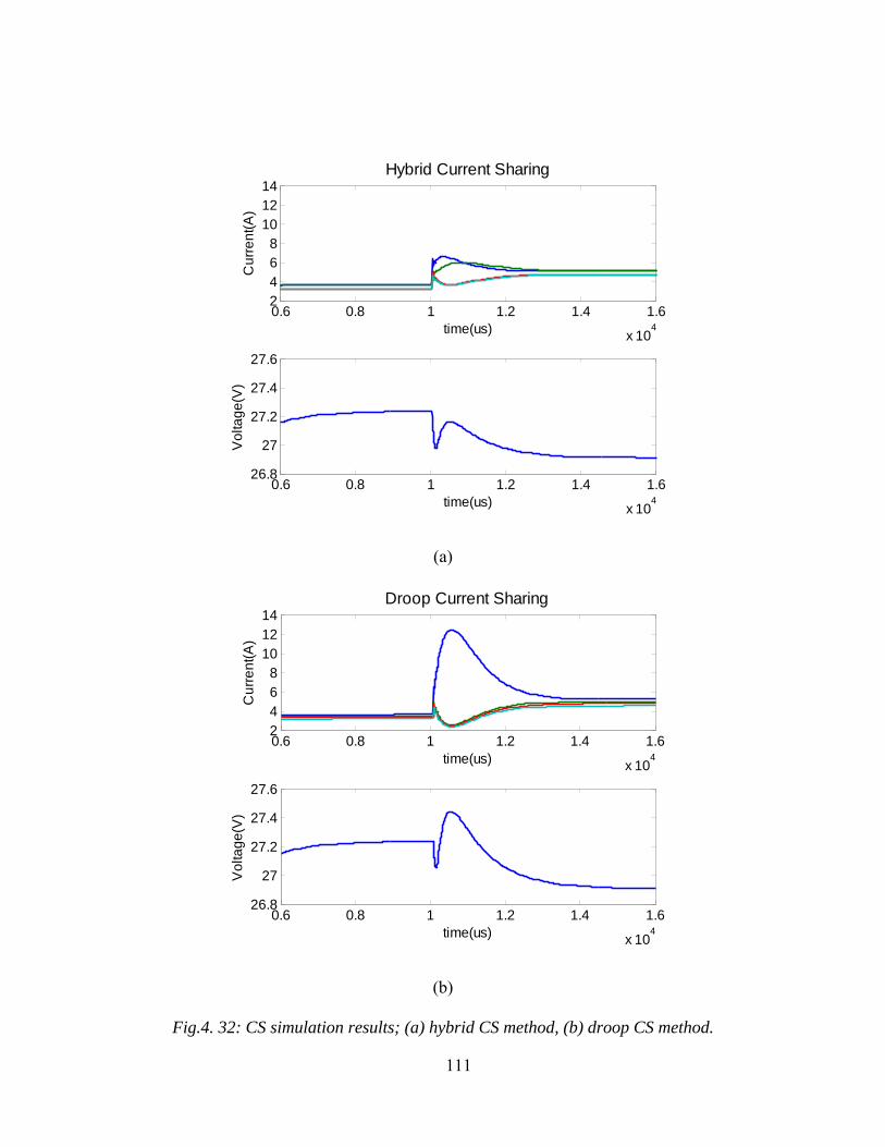
111
0.6 0.8 1 1.2 1.4 1.6
x 104
2468
101214
time(us)
Cur
rent
(A)
Hybrid Current Sharing
0.6 0.8 1 1.2 1.4 1.6
x 104
26.8
27
27.2
27.4
27.6
time(us)
Vol
tage
(V)
(a)
0.6 0.8 1 1.2 1.4 1.6
x 104
2468
101214
time(us)
Cur
rent
(A)
Droop Current Sharing
0.6 0.8 1 1.2 1.4 1.6
x 104
26.8
27
27.2
27.4
27.6
time(us)
Vol
tage
(V)
(b)
Fig.4. 32: CS simulation results; (a) hybrid CS method, (b) droop CS method.

112
4.4.2. Synchronization Among Different Channels
Since each channel has its own DSP controller and each DSP has its own timing circuitry, when
multiple channels are paralleled, timing circuitry drifting can be observed. Furthermore,
switching frequency at the level of 100 kHz is drifting. Due to small impedance among different
channels’ ports, even small voltage ripple can cause large current ripple, which is shown in
Figure 4.34. Therefore synchronization is necessary and the “wireless” solution would be
preferred due to the noise issue of wiring and the freedom to place the converter channels at
different locations closer to users. The block diagram implementation method is illustrated in
Figure 4.33(a). The output voltage has the ripple actually including the switching frequency and
exact switching point information. By processing this signal, DSP synchronization could be
achieved. The original output voltage signal V0 will be first filtered to obtain an average value of
V1, deducted by V0 and then amplified by coefficient K to be V2, finally comparing with some
preset value to generate a square waveform which feeds back into DSP to trigger the PWM
counter. By this way, every DSP can be synchronized by the same signal, which is output
voltage. In our design, the falling edge is used to trigger PWM counters.
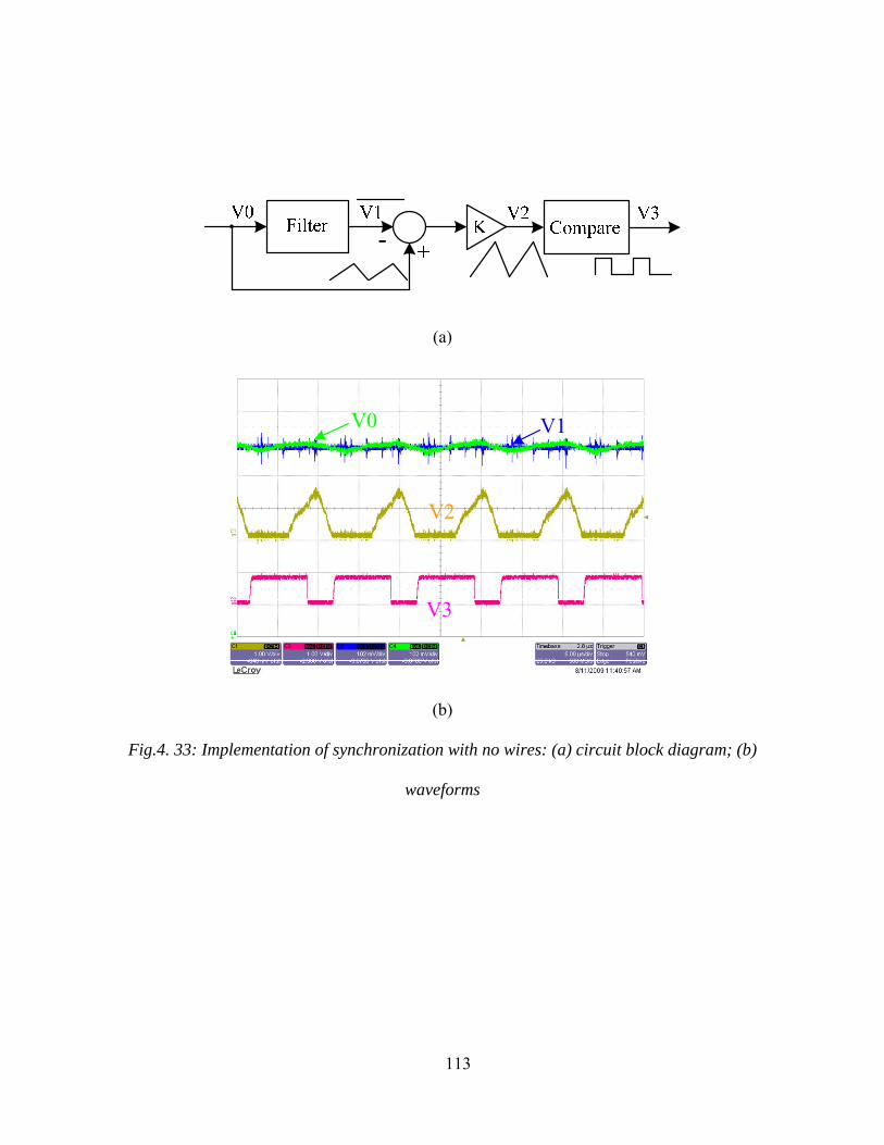
113
(a)
V0 V1
V2
V3
(b)
Fig.4. 33: Implementation of synchronization with no wires: (a) circuit block diagram; (b)
waveforms
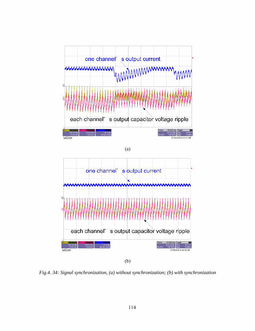
114
(a)
(b)
Fig.4. 34: Signal synchronization, (a) without synchronization; (b) with synchronization

115
4.5. Experiments for Multiple Three-port Converters
The three-port converter system is verified through a two-channel four-converter prototype rated
at 800W as shown in Figure 4.35. Figure 4.36 gives the output port CS performance. Hybrid CS
has better load transients than conventional droop method. It should be noted that the proposed
hybrid CS does not affect steady state CS performance as the droop rate is the same for both
methods. As in Figure 4.37, the output voltage has no spike when one channel fails, which
implies the fault-tolerant feature of the multi-channel converters.
Fig.4. 35: Prototype photo of two converter channels
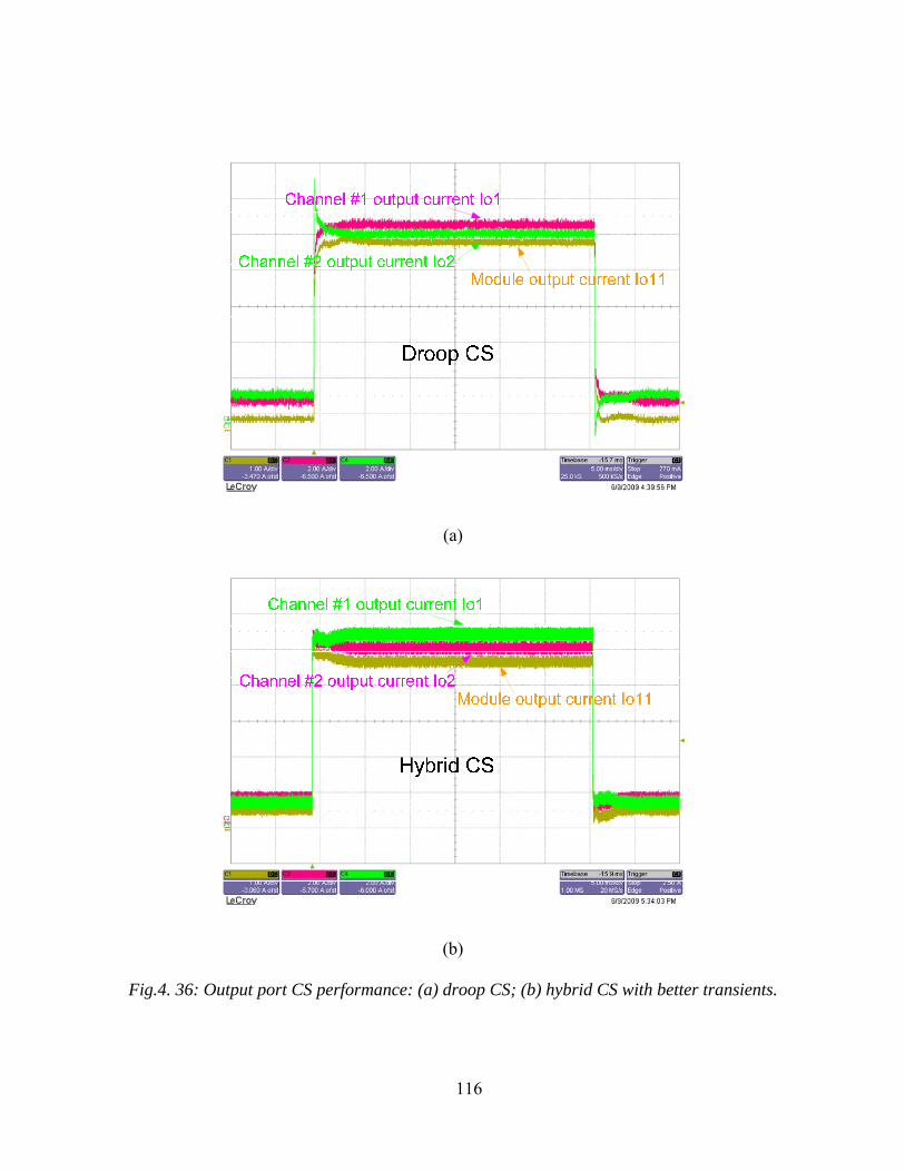
116
(a)
(b)
Fig.4. 36: Output port CS performance: (a) droop CS; (b) hybrid CS with better transients.

117
Fig.4. 37: One channel fails while the other channel is not affected.
Figure 4.38 shows that input CS compatible with MPPT algorithm, and even during solar
irradiance level changes, input currents agree with each other. Figure 4.39(a) shows that both
channels are working under MPPT to maximize solar power, while battery port provides the
power balance for the system when the load power changes, and two PV panel have very
different maximum power points. Figure 4.39(b) shows that one channel goes to regulate battery
port first because its upper voltage limit has been reached, and then followed by the other
channel when the other voltage limit is met. The reason is that although Vbmax and Rdroop are the
same, two channels have different Ib, as a result, their voltage settings are different. Therefore,
from Figure 4.39, the proposed autonomous mode transition allows smooth transition for
independent channels under different conditions.
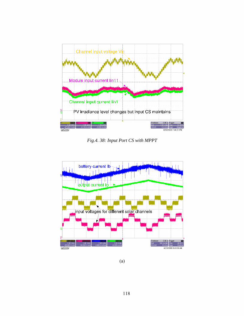
118
Fig.4. 38: Input Port CS with MPPT
(a)

119
output voltage Vo
battery voltage Vb
input voltages for different solar channelsthis channel goes into battery regulation first
(b)
(c)
Fig.4. 39: Autonomous mode transitions: (a) both with MPPT; (b) transit from both with MPPT
to one with MPPT ; (c) transit from one with MPPT to both without MPPT.

120
CHAPTER 5: AN INTEGRATED FOUR-PORT DC/DC CONVERTER
5.1. General Description
As interest in renewable energy systems with various sources becomes greater than before, there
is a supreme need for integrated power converters that are capable of interfacing and
concurrently controlling several power terminals with low cost and compact structure.
Meanwhile, due to the intermittent nature of renewable sources, a battery backup is normally
required when the ac mains is not available.
This Chapter proposes a new four-port integrated DC/DC topology, which is suitable for various
renewable energy harvesting applications. An application interfacing hybrid photovoltaic (PV)
and wind sources, one bi-directional battery port and an isolated output port is given as a design
example. It can achieve maximum power point tracking (MPPT) for both PV and wind power
simultaneously or individually, while maintaining a regulated output voltage.
The proposed four-port DC/DC converter interface has bidirectional capability and also one
isolated output. Its main components are only four main switches, two diodes, one transformer,
and one inductor. Moreover, zero-voltage switching (ZVS) can be achieved for all main switches
to allow higher efficiency at higher switching frequency, which will lead to more compact design
of this multi-port converter. The control design is also investigated based on the modeling of this
modified half-bridge topology. In addition, a decoupling network is introduced to allow the
separate controller design for each power port. Finally, a prototype has been built to verify the
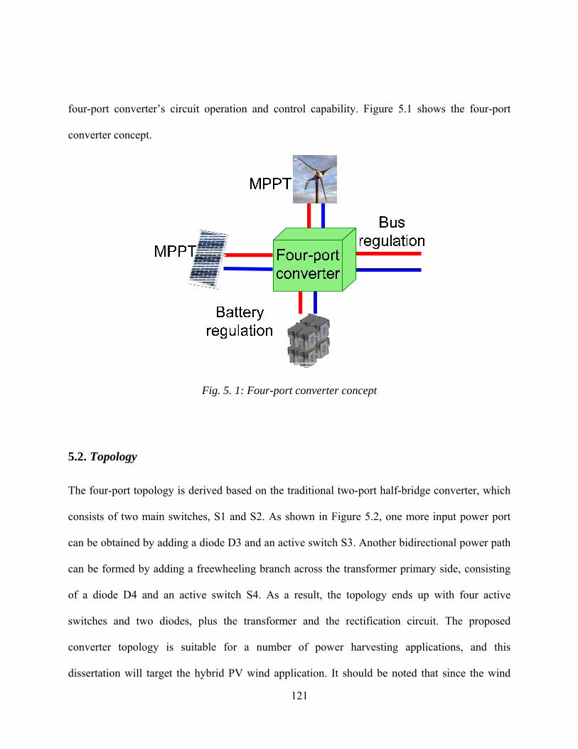
121
four-port converter’s circuit operation and control capability. Figure 5.1 shows the four-port
converter concept.
Fig. 5. 1: Four-port converter concept
5.2. Topology
The four-port topology is derived based on the traditional two-port half-bridge converter, which
consists of two main switches, S1 and S2. As shown in Figure 5.2, one more input power port
can be obtained by adding a diode D3 and an active switch S3. Another bidirectional power path
can be formed by adding a freewheeling branch across the transformer primary side, consisting
of a diode D4 and an active switch S4. As a result, the topology ends up with four active
switches and two diodes, plus the transformer and the rectification circuit. The proposed
converter topology is suitable for a number of power harvesting applications, and this
dissertation will target the hybrid PV wind application. It should be noted that since the wind

122
turbine normally generates a three-phase AC power, an AC/DC rectifier needs to be installed
before this four-port DC/DC interface and after the wind turbine output. The rectification stage
can utilize either active Power Factor Correction (PFC) or passive PFC. However, it should be
noted that the AC/DC solution is beyond the scope of this paper.
Fig. 5. 2: The four-port half-bridge converter topology, which can achieve ZVS for all four main
switches (S1, S2, S3 and S4) and adopts synchronous rectification for the secondary side to
minimize conduction loss.
As shown in Figure 5.2, the derived four-port modified half-bridge converter provides three
independent control variables, namely duty-cycles d1, d2 and d3 to control S1, S2 and S3,
respectively, while S4 will be controlled by 1-d1-d2-d3. This allows tight control over three of the
converter ports, while the fourth port provides the power balance in the system. The switching
sequence ensures a clamping path for the energy of the leakage inductance of the transformer.
This energy is further utilized to achieve zero-voltage switching (ZVS) for all primary switches
for a wide range of source and load conditions. The secondary side adopts a synchronous
rectifier to minimize the conduction loss. This also simplifies the feedback controller design,

123
because the transition from continuous conduction mode (CCM) to discontinuous conduction
mode (DCM) is avoided.
5.2.1. Driving Scheme
Figure 5.3 illustrates a possible modulation approach to realize the constant frequency pulse
width modulation (PWM) control. Where VSAW is the SAW carrier waveform for modulation,
VC1, VC2 and VC3 are control voltages derived from the voltage or current feedback controllers.
By modulating these control voltages, driving signals for S1, S2 and S3 can be generated,
respectively. Then by reversing S1 and S3 driving signals, S4 and two SR signals can be
obtained. It should be noted that S2, S3 and S4 do not need to be gated on at the same time;
instead, S3 is only required to turn on a little earlier before S2 turns off, and S4 is only required
to turn on a little earlier before S3 turns off. No dead time is necessary between S2 and S3, nor
between S3 and S4, because the existing of diodes can prevent shoot-through problems. But the
dead time between S1 and S2 and between S1 and S4 is necessary to prevent shoot-through, and
also to create ZVS conditions for S1 and S2.
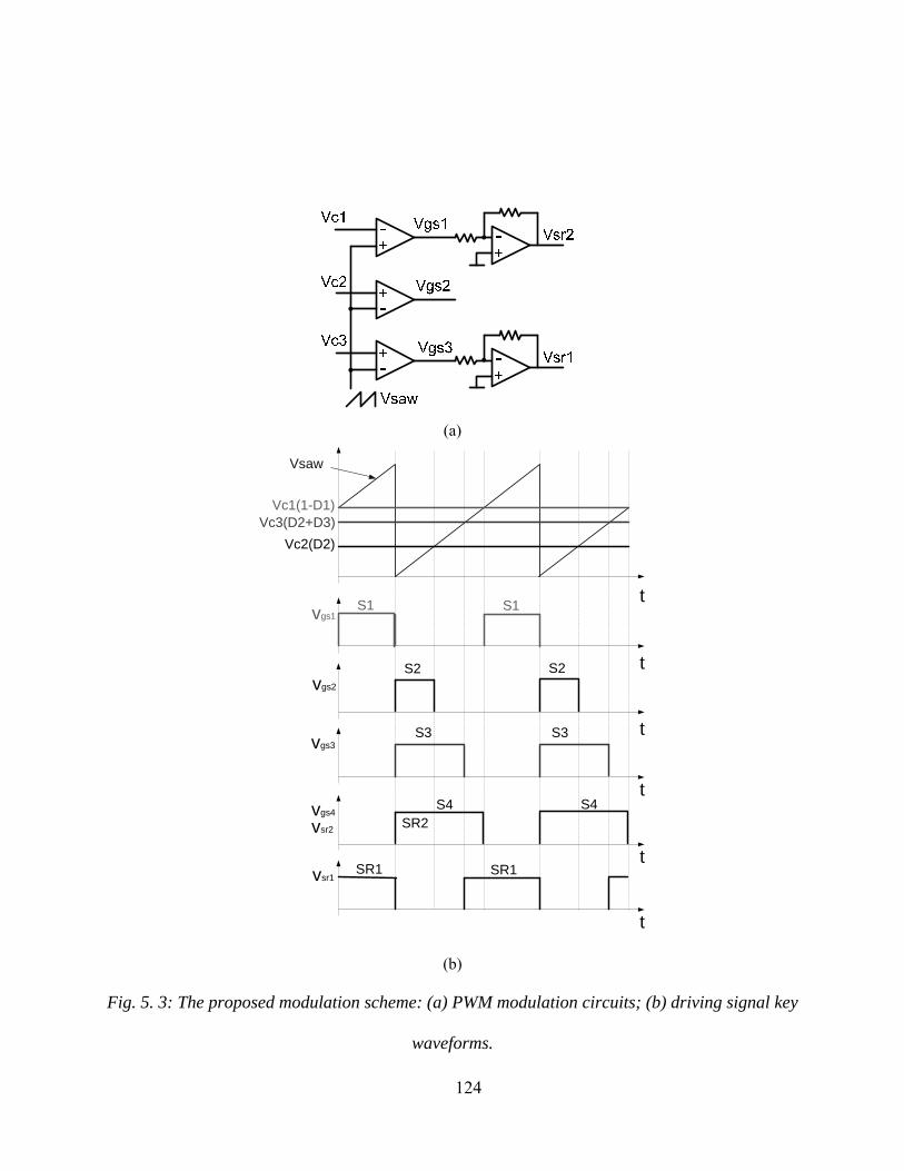
124
(a)
t
S2vgs2
S3vgs3
t
S4vgs4
t
S2
S3
S4
Vc1(1-D1)Vc3(D2+D3)
S1S1
t
SR1vsr1
vsr2
vgs1
SR2
Vsaw
t
t
Vc2(D2)
SR1
(b)
Fig. 5. 3: The proposed modulation scheme: (a) PWM modulation circuits; (b) driving signal key
waveforms.

125
5.2.2. Circuit Operation Principles
The steady-state waveforms of the four-port converter are shown in Figure 5.4, and the various
operation stages in one switching cycle are shown in Figure 5.5. To simplify the analysis of
operation, components are considered ideal except otherwise indicated. The main operation
stages are described as follows.
Stage 1 (t0-t1): Before this stage begins, the body diode of S1 is forced on to recycle the energy
stored in the transformer leakage inductor, and the output is freewheeling. At time t0, S1 is gated
on with ZVS, and then the leakage inductor is reset to zero and reverse-charged.
Stage 2 (t1-t2): At time t1, the transformer primary current increases to the reflected current of
iLo, the body diode of SR2 becomes blocked, and the converter starts to deliver power to the
output.
Stage 3 (t2-t3): At time t2, S1 is gated off, causing the leakage current ip to charge the S1
parasitic capacitor and discharge the S2, S3 and S4 parasitic capacitors.
Stage 4 (t3-t4): At time t3, the voltage across the S2 parasitic capacitor is discharged to zero, and
the S2 body diode conducts to carry the current, which provides the ZVS condition for S2.
During this interval, the output is freewheeling through SR1 and SR2 body diodes.
Stage 5 (t4-t5): At time t4, S2 is gated on with ZVS, and then the leakage inductor is reset to zero
and reverse-charged. The output inductor current drop from t2 to t5 is due to the leakage inductor
discharge/charge.

126
Stage 6 (t5-t6): At time t5, the transformer primary current increases to the reflected current of
iLo, the body diode of SR1 is blocked, and the converter starts to deliver power to the output.
Stage 7 (t6-t7): At time t6, S2 is gated off, causing the leakage current ip to charge the S2
parasitic capacitor and discharge the S1 and D3 parasitic capacitors.
Stage 8 (t7-t8): At time t7, the voltage across D3 is discharged to zero, and then D3 conducts. S3
is gated on before this time, so S3 has natural ZVS. Output inductor current freewheels through
SR2 during this period.
Stage 9 (t8-t9): At time t8, S3 is gated off, causing the leakage current ip to charge S2 and S3
parasitic capacitors and discharge S1 and D4 parasitic capacitors.
Stage 10 (t9-t10): At time t9, the voltage across D4 is discharged to zero, and D4 conducts. Since
S4 is gated on before this time, the leakage current freewheels through D4 and S4 so that the
leakage energy is trapped. On the secondary side, output inductor current freewheels through
SR1 and SR2.
Stage 11 (t10-t11): At time t10, S4 is gated off, causing the trapped leakage energy to discharge
the S1 parasitic capacitor and charge the S2, S3 and S4 parasitic capacitors.
Stage 12 (t11-t12): At time t11, the voltage across S1 is discharged to zero, and the S1 body
diode conducts to carry the current, which provides ZVS condition for S1. During this interval,
the output is freewheeling. This is the end of the switching cycle.
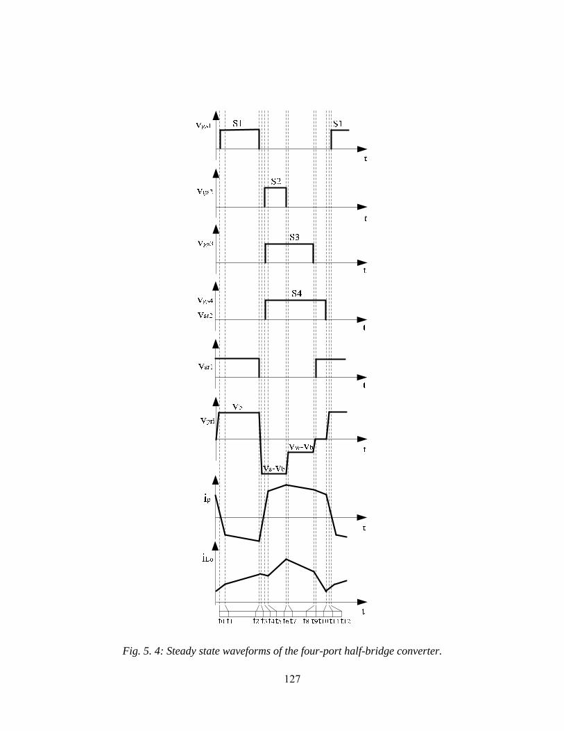
127
Fig. 5. 4: Steady state waveforms of the four-port half-bridge converter.
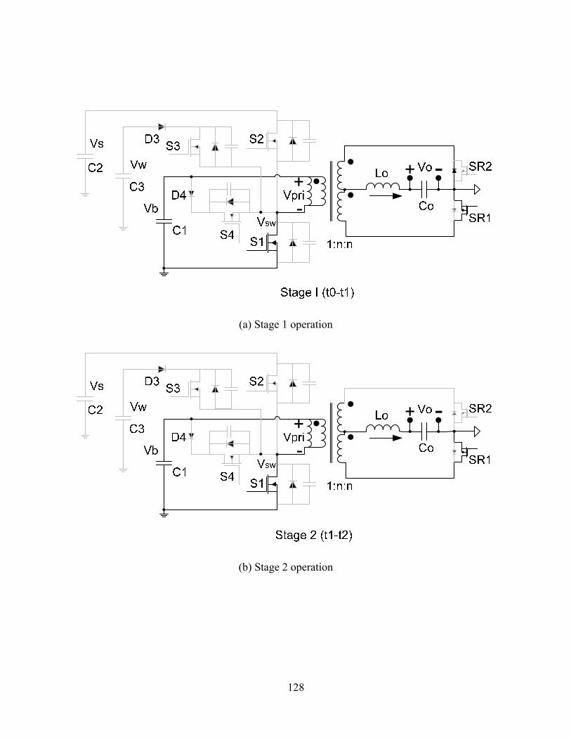
128
(a) Stage 1 operation
(b) Stage 2 operation
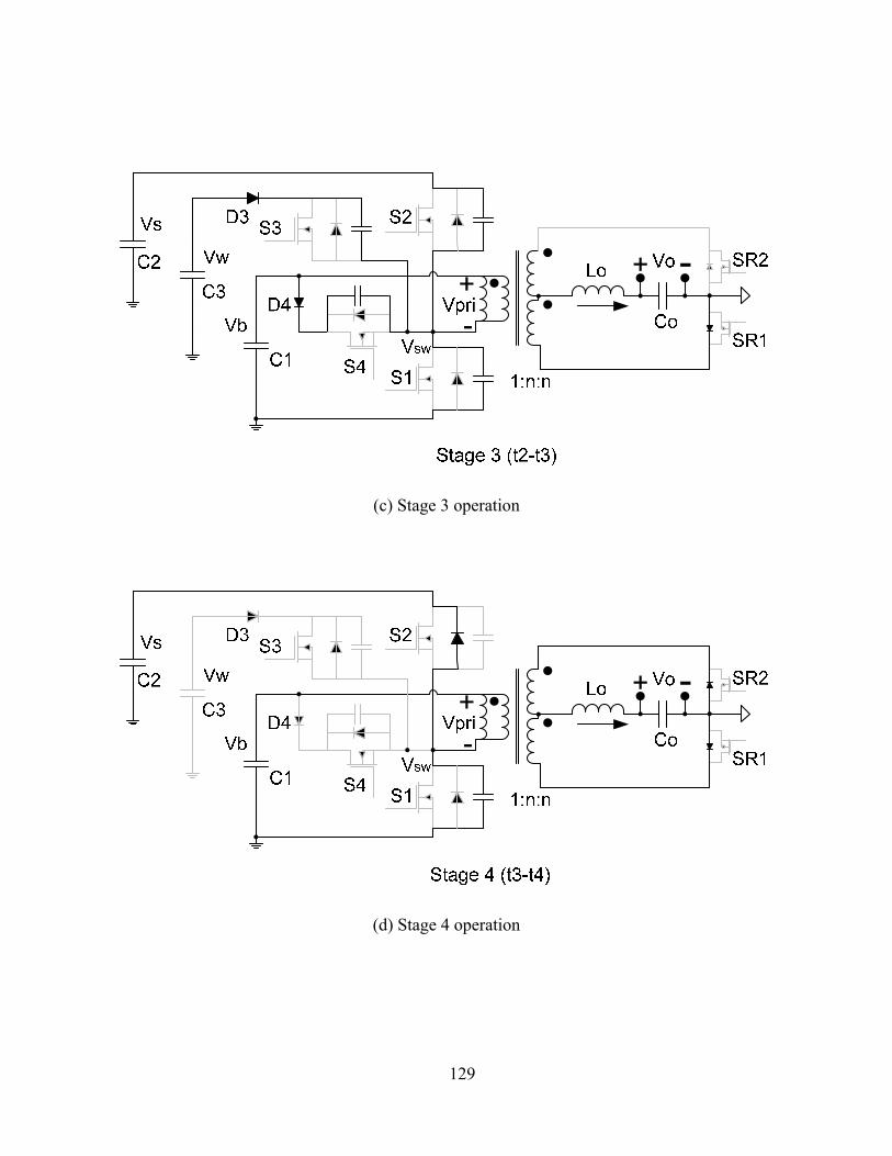
129
(c) Stage 3 operation
(d) Stage 4 operation
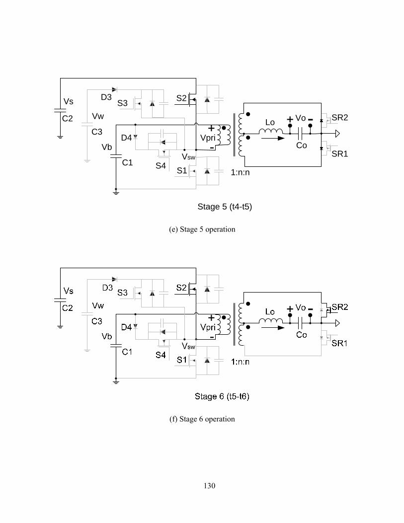
130
Stage 5 (t4-t5)
S1S4
S2
C2
C1
D4
1:n:n
Vs
VbVsw
C3
S3
Vpri
Lo
Co
Vo
SR1
SR2Vw
D3
(e) Stage 5 operation
(f) Stage 6 operation
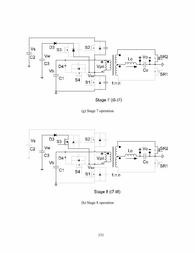
131
(g) Stage 7 operation
(h) Stage 8 operation
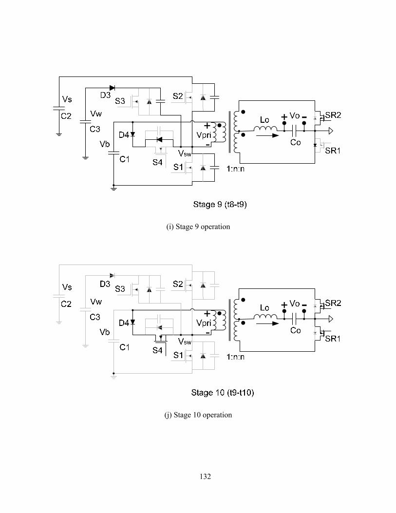
132
(i) Stage 9 operation
(j) Stage 10 operation
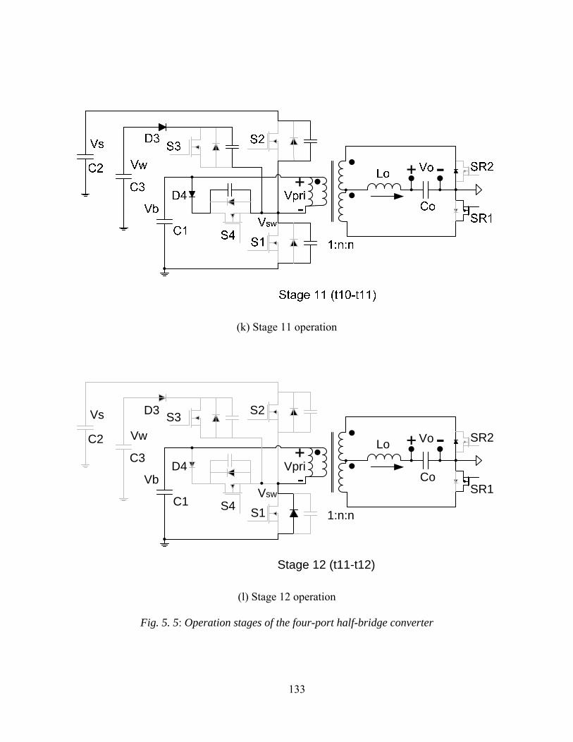
133
(k) Stage 11 operation
Stage 12 (t11-t12)
S1S4
S2
C2
C1
D4
1:n:n
Vs
VbVsw
C3
S3
Vpri
Lo
Co
Vo
SR1
SR2Vw
D3
(l) Stage 12 operation
Fig. 5. 5: Operation stages of the four-port half-bridge converter

134
5.2.3. Steady State Analysis
Assuming an ideal converter, the steady-state voltage governing relations between different port
voltages can be determined by equating the voltage-second product across the converter’s two
main inductors to zero. First, using volt-second balance across the primary transformer
magnetizing inductance LM, in CCM, we have:
1 2 3( ) ( )b s b w bV D V V D V V D⋅ = − ⋅ + − ⋅ Eq. 5.1
Assuming CCM operation, the voltage-second balance across the load filter inductor Lo then
yields:
1 2 3( ) ( ) /b s b w b oV D V V D V V D V n⋅ + − ⋅ + − ⋅ = Eq. 5.2
Where n is the turns ratio of the transformer, Vs, Vw, Vb, Vo are the solar input, wind input, battery
and output voltages, respectively.
The following equation is based on the power balance principle, by assuming a lossless
converter, steady-state port currents can be related as follows:
s s w w b b o oV I V I V I V I⋅ + ⋅ = ⋅ + ⋅ Eq. 5.3
Where Is, Iw, Ib, Io are the average solar input, wind input, battery bidirectional, and load currents,
respectively. The battery current Ib is positive during charging, and negative during discharging.
5.2.4. ZVS Analysis
ZVS of the switches S1 and S2 can be realized through the energy stored in the transformer
leakage inductor, while ZVS of S3 and S4 is always maintained, because the proposed driving

135
scheme ensures that paralleling diodes of S3 and S4 will be forced on before the two switches
turn on.
After S4 is turned off, the leakage energy is released to discharge the S1 parasitic capacitor and
charge S2, S3 and S4’s parasitic capacitors, to create the ZVS condition of S1. And the following
condition should be satisfied:
2 21 ( ) 2 , 02 k M o oss b oss s b oss w b M oL I n I C V C V V C V V I n I⋅ ⋅ + ⋅ > ⋅ ⋅ + ⋅ ⋅ + ⋅ ⋅ + ⋅ > Eq. 5.4
Where Lk is the transformer leakage inductance, MOSFET parasitic capacitances of S1, S2, S3
and S4 are assumed to be equal as Coss, and IM is the average transformer magnetizing current
which satisfies:
( ) ( ) ( )1 2 3b M o M o M oI D I n I D I n I D I n I= ⋅ − ⋅ + ⋅ + ⋅ + ⋅ + ⋅ Eq. 5.5
Rearranging (5), we can obtain IM as follows:
( )1 2 3
1 2 3
b oM
I D D D n II
D D D+ − − ⋅ ⋅
=+ +
Eq. 5.6
After S1 is turned off, the leakage energy will charge the S1 parasitic capacitor and discharge S2,
S3 and S4’s parasitic capacitors to achieve ZVS for S2:
2 2 2 21 1 1( ) , 02 2 2k M o oss s oss w oss b M oL I n I C V C V C V I n I⋅ ⋅ − ⋅ > ⋅ + ⋅ ⋅ + ⋅ ⋅ − ⋅ < Eq. 5.7
According to equation 5.7, when the load current Io is small and the transformer magnetizing
current IM is large, IM-n Io <0 can not be met. In other words, ZVS of S2 will be lost. However,
in most load/source conditions, ZVS of S2 is achievable.

136
It should be noted that ZVS of S3 and S4 can be naturally achieved if the voltage relation
b w sV V V< < is satisfied to ensure that the paralleling diodes will always be forced on before
these switches turn on. On one hand, w sV V< is not difficult to meet since the solar port and wind
port can be reversed if the wind port voltage Vw is larger than the solar port voltage Vs. Even if
Vw is not always lower than Vs in the whole voltage ranges, the converter itself still works, but
may lose some conduction period for the S2 branch depending on the driving overlap of S2 and
S3. The solution is to change the driving scheme to avoid the S2 and S3 overlap. On the other
hand, it is a step-down conversion from PV or wind port to battery port, therefore the battery
voltage Vb will be always lower than the PV voltage Vs and the wind source voltage Vw.
To sum up, ZVS of all main switches can be achieved to maintain higher efficiency when the
converter is operated at higher switching frequency, because of the potential savings in switching
losses.
5.2.5. Circuit Design Considerations
When considering the semiconductor stresses, this modified half-bridge topology shows striking
similarity to its traditional half-bridge counterpart. The major difference is that the transformer
design of this four-port converter needs to allow for a dc current flow and therefore becomes
similar to an inductor or a flyback transformer design. The dc biasing current rating is dictated
by equation 5.6, which determines the amount of the air gap to be inserted. Other than the
transformer, the circuit design and optimization technique used for the traditional half-bridge

137
topology can be used here for this four-port topology, which provides great convenience for the
practicing engineers to implement the power stage design.
5.2.6. Semiconductor Stresses
The ideal reverse voltages seen by the switches on the primary side are:
1 2S S sV V V= =
3S wV V=
4S biV V= Eq. 5.8
Because at the starting point the wind port and battery port may not be able to build the voltage if
the solar port is connected first, the voltage stresses seen by the diodes D3 and D4 are the same.
3D sV V=
4D sV V= Eq. 5.9
Assuming CCM operation, and neglecting inductor ripple currents, the rms current in the
primary switches are given by:
1 1rmsS o MI D nI I= ⋅ −
2 2rmsS o MI D nI I= ⋅ +
3 3rmsS o MI D nI I= ⋅ +
3 1 2 31rmsS o MI D D D nI I= − − − ⋅ + Eq. 5.10
The average current of carried by D3 and D4 are:

138
( )3 3avgD o MI D nI I= ⋅ +
( ) ( )4 1 2 31avgD o MI D D D nI I= − − − ⋅ + Eq. 5.11
Note that it is assumed that the primary leakage inductance carries the reflected load current.
The average currents through the secondary side rectifiers are:
1 2 3(1 )avgSR oI D D I= − − ⋅
( )2 11avgSR oI D I= − ⋅ Eq. 5.12
Assuming perfect snubbing (no ringing), the ideal voltage stresses seen by the rectifier diodes or
synchronous switches of a center-tapped rectifier are:
( )1 2SR s biV n V V= ⋅ −
2 2SR biV n V= ⋅ Eq. 5.13
5.2.7. Transformer Turns Ratio
Stress analysis clearly shows that the turns’ ratio of the transformer has a major effect on circuit
components stresses. A higher turns’ ratio increases the circulating currents on the primary side,
translating to higher switch currents and a higher dc magnetizing current. It also increases the
voltage at the secondary side, applying higher reverse voltages to the rectifier devices. A
minimum turns’ ratio, however, is necessary to maintain the ability to achieve the targeted output
voltage level with an acceptable head-room for regulation. The proper choice of turns’ ratio is
strongly dependent on the voltage specifications at the different ports.

139
5.3. Modeling and Control
This section introduces the modeling and control for the four-port converter. The modeling
follows the same procedure presented in Chapter 3. There are various modes of operation for the
four-port converter. Therefore, only the model under one operation mode is given in this section
to provide a design example. Experiments verify the controller design and further confirm its
ability to achieve tight independent control over three power processing paths.
5.3.1. Various Modes of Operation
According to whether energy sources (PV panels and Wind turbines) provide power for the load
or/and battery, whether the battery supplies or absorbs power and whether the battery connects to
the system, operation states of proposed four-directional converter can be classified into thirteen
possible stages which are listed in Table 5.1. For the PV panels and the wind turbine, supplying
power for the load or the power grid is denoted by the “1”, or by the “0”. For the battery, the “1”
indicates supplying power; whereas, the “-1” indicates absorbing power and the “0” expresses
disconnection. Moreover, for the load connection in the converter is expressed by the “1”, or by
the “0”. Power sources of the four-port converters are various for different operation stages. In
operation stage 2 and 6, power is transferred from the first input source, the second input source
to the output; while the battery sinks or sources according the source condition and load profile.
In the rest of stages, at least one port is left open. Therefore, the four-port converter can be
treated as a three-port or a traditional two-port converter. Since mode definition for the three-port

140
converter has been discussed in chapter three, in this chapter, only the four-port converter
operation including stage 2 and 6 will be focused.
Table 5.14 Operational Stages of the Four-port Converter
Operation Stages PV source Wind source battery load Stage 0 0 0 1 1 Stage 1 0 1 1 1 Stage 2 1 1 1 1 Stage 3 0 1 0 1 Stage 4 1 0 0 1 Stage 5 0 1 -1 1 Stage 6 1 1 -1 1 Stage 7 1 1 0 1 Stage 8 1 0 1 1 Stage 9 1 0 -1 1
Stage 10 1 0 -1 0 Stage 11 1 1 -1 0 Stage 12 0 1 -1 0
Generally speaking, stable system operation requires the maintenance of power balance in the
system. That is, in steady-state, the sum of average input power to the converter is required to
equal the sum of average output power plus any power losses. This implies that, for a four-port
system, the operating point of up to three ports can be tightly regulated, while the fourth port
should be kept “flexible” and would operate at any point that satisfies the power balance
constraints.
The choice of the flexible power port dictates the feedback control layout. It can be either of the
following: the solar port, the wind port, the battery port or the output port. But normally, the
output port connecting to the load is preferred to be regulated. So there are three modes to be
defined.

141
In Battery-balanced Mode, the load voltage is tightly regulated; both the PV panel and the wind
turbine operate under MPPT control to provide maximum power. The battery preserves the
power balance for the system by storing unconsumed solar power or by providing the deficit
during high load intervals. This mode is desirable since it can harvest the maximal power from
both PV array and the wind turbine.
In Excess-insolation Mode, the load is regulated and sinks less power than is available, while the
battery charge rate is limited. In this case, the battery current or voltage is regulated, while the
solar array is forced to operate in its voltage-source region where it provides less power than it
has available. The wind turbine is operating under MPPT to maximize the wind power
harvesting.
In Excess-wind Mode, the load is regulated and sinks less power than is available, while the
battery charge rate is limited. In this case, the battery current or voltage is regulated, while the
wind turbine output is forced to operate in its left side I-V curve to limit the power. The PV array
is operating under MPPT to maximize the solar power harvesting.
In the next section, the battery-balanced mode will be focused since it is the preferred mode of
operation.
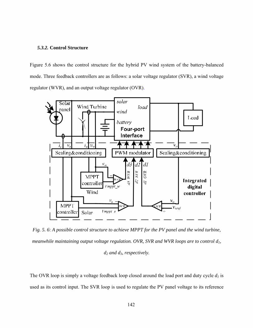
142
5.3.2. Control Structure
Figure 5.6 shows the control structure for the hybrid PV wind system of the battery-balanced
mode. Three feedback controllers are as follows: a solar voltage regulator (SVR), a wind voltage
regulator (WVR), and an output voltage regulator (OVR).
Fig. 5. 6: A possible control structure to achieve MPPT for the PV panel and the wind turbine,
meanwhile maintaining output voltage regulation. OVR, SVR and WVR loops are to control d1,
d2 and d3, respectively.
The OVR loop is simply a voltage feedback loop closed around the load port and duty cycle d1 is
used as its control input. The SVR loop is used to regulate the PV panel voltage to its reference
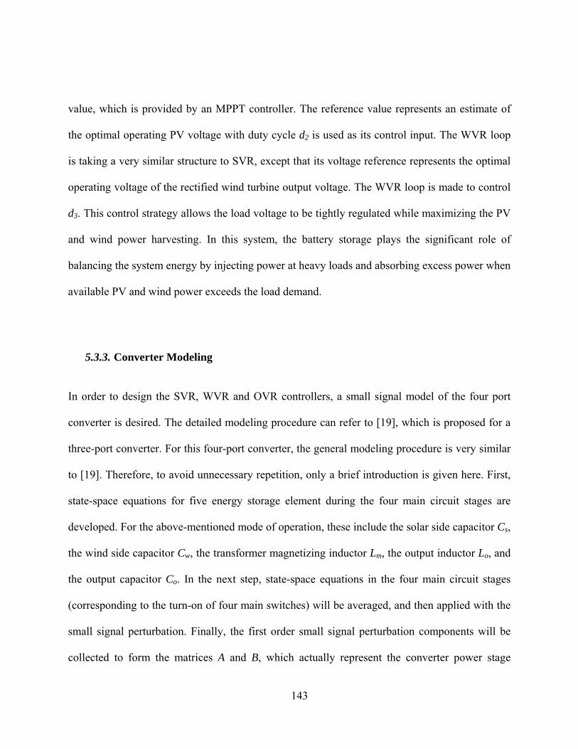
143
value, which is provided by an MPPT controller. The reference value represents an estimate of
the optimal operating PV voltage with duty cycle d2 is used as its control input. The WVR loop
is taking a very similar structure to SVR, except that its voltage reference represents the optimal
operating voltage of the rectified wind turbine output voltage. The WVR loop is made to control
d3. This control strategy allows the load voltage to be tightly regulated while maximizing the PV
and wind power harvesting. In this system, the battery storage plays the significant role of
balancing the system energy by injecting power at heavy loads and absorbing excess power when
available PV and wind power exceeds the load demand.
5.3.3. Converter Modeling
In order to design the SVR, WVR and OVR controllers, a small signal model of the four port
converter is desired. The detailed modeling procedure can refer to [19], which is proposed for a
three-port converter. For this four-port converter, the general modeling procedure is very similar
to [19]. Therefore, to avoid unnecessary repetition, only a brief introduction is given here. First,
state-space equations for five energy storage element during the four main circuit stages are
developed. For the above-mentioned mode of operation, these include the solar side capacitor Cs,
the wind side capacitor Cw, the transformer magnetizing inductor Lm, the output inductor Lo, and
the output capacitor Co. In the next step, state-space equations in the four main circuit stages
(corresponding to the turn-on of four main switches) will be averaged, and then applied with the
small signal perturbation. Finally, the first order small signal perturbation components will be
collected to form the matrices A and B, which actually represent the converter power stage

144
model. It should be noted that the symbolic derivation of these transfer functions is fairly
tedious. Alternatively, the dynamics of the plant can be calculated by computer software like
MATLAB®. The resultant state-space averaging model takes the following form:
/ ,dX dt A X B U Y I X= ⋅ + ⋅ = ⋅ Eq. 5.15
2 2
3 3
32
32
1 0 0
1 ˆ0 0ˆˆ0 0 0 , ˆ
10 0 ˆ
1 10 0 0
0 0
0 0
s s s s
sw w w w
w
LmM M
Lo
oo o o
o o
oLm
s
oLm
w
b s b w b
M M
D n DR C C C
D n D vR C C C
vDD
A X iL L
in Dn D
vL L L
C R C
n VI RC
n VI RC
BV V V V VL L
− − ⋅⎡ ⎤−⎢ ⎥⋅⎢ ⎥− − ⋅⎢ ⎥− ⎡ ⎤⎢ ⎥⋅ ⎢ ⎥⎢ ⎥
⎢ ⎥⎢ ⎥⎢ ⎥= =⎢ ⎥⎢ ⎥⎢ ⎥⎢ ⎥⎢ ⎥⋅⋅ − ⎢ ⎥⎢ ⎥ ⎣ ⎦
⎢ ⎥⎢ ⎥
−⎢ ⎥⋅⎣ ⎦⋅− −
⋅− −
=− −
−
1, 2
3
( ) ( )
0 0 0
M
b s b w b
o o o
dU d
dL
n V n V V n V VL L L
⎡ ⎤⎢ ⎥⎢ ⎥⎢ ⎥⎢ ⎥⎢ ⎥ ⎡ ⎤⎢ ⎥ ⎢ ⎥=⎢ ⎥ ⎢ ⎥⎢ ⎥ ⎢ ⎥⎣ ⎦⎢ ⎥⎢ ⎥
⋅ ⋅ − ⋅ −⎢ ⎥⎢ ⎥⎢ ⎥⎣ ⎦ Eq. 5.16
Where X is a matrix containing the state variables Vs, Vw, iLm, iLo, and Vo, U is a matrix containing
the control inputs d1, d2 and d3, Y is a matrix containing the system outputs, and I is the identity
matrix.
With matrices A and B, transfer functions for PV, wind and output voltages to different duty-
cycle values can be extracted according to equation 5.16. For example, G(s)(5,1) represents the
5th state variable Vo and the 1st control variable d1, thus equals to open loop transfer function of
145
Vo(s)/ d1(s). So the row number denotes the sequence of state variable, and the column number
denotes that of control input.
( ) 1
11 21 31
12 22 32
13 23 33
,( )(5,1) , ( )(1,1), ( )(2,1)( )(5,2) , ( )(1,2), ( )(2,2)( )(5,3) , ( )(1,3), ( )(2,3)
G s I A Bg G s g G s g G sg G s g G s g G sg G s g G s g G s
−= ⋅ − ⋅
= = =
= = =
= = = Eq. 5.17
Figure 5.7 illustrates the small signal model diagram when closing SVR, WVR and OVR loops,
which consists of the converter model and the feedback controllers. FM represents the PWM
modulator gain and different KV values represent different voltage signal sensing gains, which
can be treated as the fixed proportional values.
Fig. 5. 7: Small signal model diagram, control inputs and outputs are decoupled to enable
separate controller design. The far right signals are routed to the far left ones in this diagram.
Vsref, Vwref and Voref are the references for solar, wind and output voltages, respectively. HSVR,
HWVR and HOVR are the compensators need to be designed.

146
5.3.4. Decoupling Method
As can be seen from Figure 5.7, the three control loops are coupled with each other, which make
it difficult to design close loop compensators for each control loop. Therefore a decoupling
network as shadowed in Figure 5.7 is introduced so that the control loops can be designed
independently with different control loop bandwidth requirement. Since output port voltage
regulation requirement is the most stringent of the three and the PV panel and wind turbine
characteristics are relatively slower, the SVR loop is designed to have a one decade lower
bandwidth than that of OVR. Moreover, WVR bandwidth can be set to be lower than that of
SVR to further reduce SVR and WVR loop interactions, since the mechanical behavior of wind
blades is slower than the photovoltaic behavior of PV panels.
The derivation of decoupling network G∗ is described as follows: the state vector matrix X can
be written as X G U ∗= ⋅ , where U ∗ is the modified input vector made up of duty cycles U,
U G U∗ ∗= ⋅ . Therefore, X G G U∗= ⋅ ⋅ . According to modern control theory, our goal is to make
G G∗⋅ a diagonal matrix to allow one control input to determine one output independently. So
based on 1 1G G X U∗ − −= ⋅ ⋅ , the decoupling matrix G∗ can be derived and simplified as:
13 32 12 33 12 23 13 22
* * * 11 33 13 31 11 22 12 2111 12 13* * * 23 31 21 33 13 21 11 2321 22 23
22 33 23 32 11 22 12 21* * *31 32 33
21 32 22 31
22 33 23
1
1
g g g g g g g gg g g g g g g g
g g gg g g g g g g gG g g gg g g g g g g g
g g gg g g gg g g g
∗
⋅ − ⋅ ⋅ − ⋅⋅ − ⋅ ⋅ − ⋅
⎡ ⎤⋅ − ⋅ ⋅ − ⋅⎢ ⎥= =⎢ ⎥ ⋅ − ⋅ ⋅ − ⋅⎢ ⎥⎣ ⎦ ⋅ − ⋅⋅ − ⋅
12 31 11 32
32 11 33 13 31
1g g g gg g g g
⎡ ⎤⎢ ⎥⎢ ⎥⎢ ⎥⎢ ⎥⎢ ⎥⎢ ⎥⋅ − ⋅⎢ ⎥
⋅ − ⋅⎣ ⎦Eq. 5.18

147
Now the cross-coupled three-loop control system is decoupled into three independent single-loop
subsystems. The system can then be controlled using independent loop controllers and each
compensator can be designed separately as well. For example, the OVR controller can then be
designed based on the following plant transfer function:
23 31 21 33 21 32 22 311 11 12 13
22 33 23 32 22 33 23 32
( ) / ( )og g g g g g g gv s d s g g gg g g g g g g g
⋅ − ⋅ ⋅ − ⋅= + ⋅ + ⋅
⋅ − ⋅ ⋅ − ⋅ Eq. 5.19
Similarly, SVR and WVR controllers can also be designed once their decoupled plant transfer
functions are derived. The controller design follows the traditional control law, and is suggested
to meet the bandwidth limitation requirement mentioned above, while having enough phase
margins to prevent potential instability. The controller normally uses the PI or PID
compensation, the design methodology has been well known to practicing engineers, therefore is
beyond the scope of this dissertation.
5.4. Experimental Results
A four-port DC/DC converter prototype is built to verify the circuit operation. The circuit
parameters are: solar port, 30-40V/1.5A; wind port, 20-30V/1.5A; battery port, 12-18V/3A;
output port, 12V/3.3A. The switching frequency is 100 kHz, and it is implemented by the digital
control to achieve the close loop regulation.

148
Figure 5.8 gives the steady state waveforms when loading the output port (a) and loading the
battery port (b). The switch node voltage Vsw shows a four-stage wave shape, corresponding to
the turn-on of four main switches with four different voltage levels. In addition, there is no CCM
and DCM transition for the output inductor current iLo, which avoids the sharp change of plant
dynamic characteristics and simplifies the output voltage feedback controller design. The
transformer magnetizing current ip is determined by both the reflected output current and the
battery current.
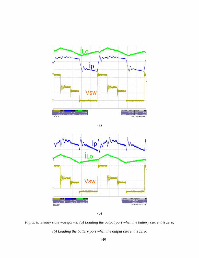
149
(a)
(b)
Fig. 5. 8: Steady state waveforms: (a) Loading the output port when the battery current is zero;
(b) Loading the battery port when the output current is zero.
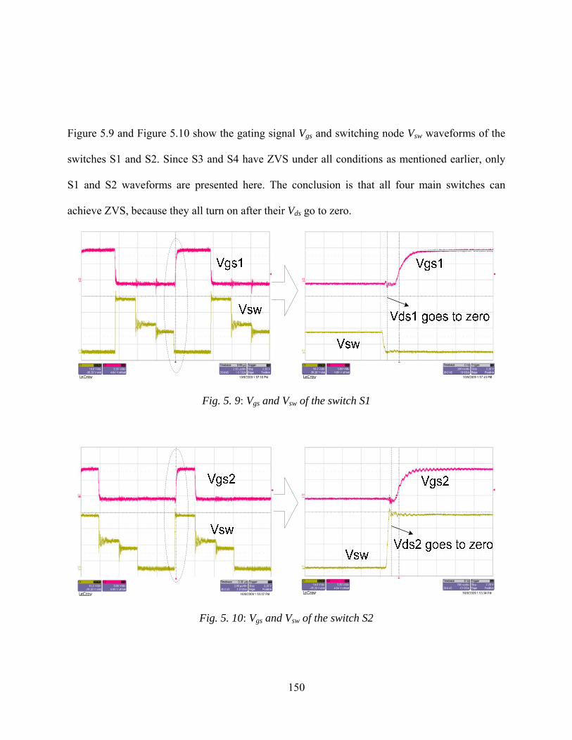
150
Figure 5.9 and Figure 5.10 show the gating signal Vgs and switching node Vsw waveforms of the
switches S1 and S2. Since S3 and S4 have ZVS under all conditions as mentioned earlier, only
S1 and S2 waveforms are presented here. The conclusion is that all four main switches can
achieve ZVS, because they all turn on after their Vds go to zero.
Fig. 5. 9: Vgs and Vsw of the switch S1
Fig. 5. 10: Vgs and Vsw of the switch S2

151
Table 5.2 shows eight different load and source combinations with each one of them to be either
10% or 90% load/source condition, while the battery port provides the power balance. The test
setup is realized by connecting the solar port and wind port of the converter to two independent
PV array simulators instead of the solar panel and the wind turbine. Then two different I-V
curves are assigned for the solar and wind port, and the DSP code is tuned so that the SVR and
WVR voltage references are at 10% or 90% rated current point. As a result, two sources will
have four different combinations. A battery is connected to sink the excess power or source the
deficit power, and the load is set to sink either 10% or 90% rated output current. So all together,
there are eight different conditions for one load and two sources as described in Table 5.2.
Table 5.20 Different Load/Source Current Level Conditions
Load/Source Current Level Conditions (%)
Vs=35.6V Vw=28.2V
Vo=12V
Case1 10 10 90
Case2 90 10 90
Case3 10 90 90
Case4 90 90 90
Case5 90 10 10
Case6 10 90 10
Case7 90 90 10
Case8 10 10 10
Figure 5.11 depicts all three port voltages under different load/source conditions. The cross
regulation of Vs, Vw and Vo are 0.5%, 0.6% and 1.1%, respectively. Figure 5.12 shows the
efficiency curve under different load/source conditions as in Table 5.2. The highest efficiency is
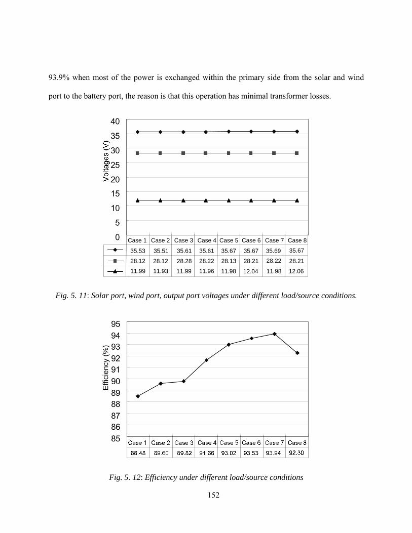
152
93.9% when most of the power is exchanged within the primary side from the solar and wind
port to the battery port, the reason is that this operation has minimal transformer losses.
Case 1 Case 2 Case 3 Case 4 Case 5 Case 6 Case 7 Case 8
35.5135.53 35.61 35.61 35.67 35.67 35.6735.69
28.12 28.12 28.28 28.22 28.13 28.21 28.22 28.21
11.99 11.93 11.99 11.96 11.98 12.04 11.98 12.06
05
10152025303540
Fig. 5. 11: Solar port, wind port, output port voltages under different load/source conditions.
8586878889909192939495
Effi
cien
cy (%
)
Fig. 5. 12: Efficiency under different load/source conditions

153
Figure 5.13 shows the transient response of the PV voltage, wind voltage and output voltage to a
load transient between 0.33A and 3A, when SVR, WVR and OVR loops are closed. In terms of
the settling time, the output voltage transient response is much faster than that of the solar or the
wind port, while the transient of the solar port is slightly faster than that of the wind port.
Because OVR bandwidth is ten times larger than that of SVR, and SVR bandwidth is four times
larger than that of WVR. As shown in Figure 5.14, Figure 5.15 and Figure 5.16, the bandwidth
designed for OVR, SVR and WVR are 2 kHz, 200 Hz and 50 Hz, respectively. The reason for
this bandwidth limitation is that the output dynamics is the most stringent of the three, while PV
panel and wind turbine dynamics are relatively slow. The above-mentioned control loop
bandwidth limitation is helpful to reduce the loop interactions.
Although the reference values of Vsref and Vwref are given as the fixed values rather than being
constantly updated by the MPPT controllers, these experiments provide a quick approximation
that MPPT of the PV panel and the wind turbine SVR can be achieved at the same time, while
maintaining a regulated output voltage.
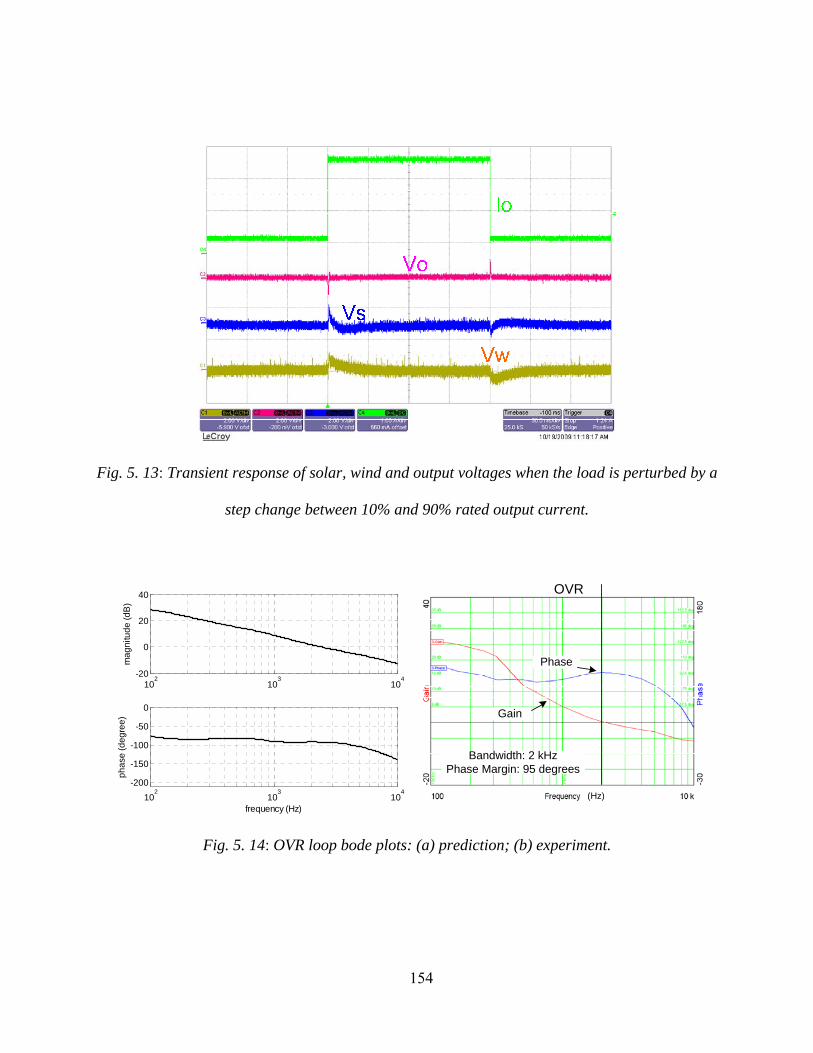
154
Fig. 5. 13: Transient response of solar, wind and output voltages when the load is perturbed by a
step change between 10% and 90% rated output current.
(Hz)
OVR
Gain
Phase
Bandwidth: 2 kHzPhase Margin: 95 degrees
102
103
104-20
0
20
40
mag
nitu
de (d
B)
102
103
104
-200
-150
-100
-50
0
frequency (Hz)
phas
e (d
egre
e)
Fig. 5. 14: OVR loop bode plots: (a) prediction; (b) experiment.
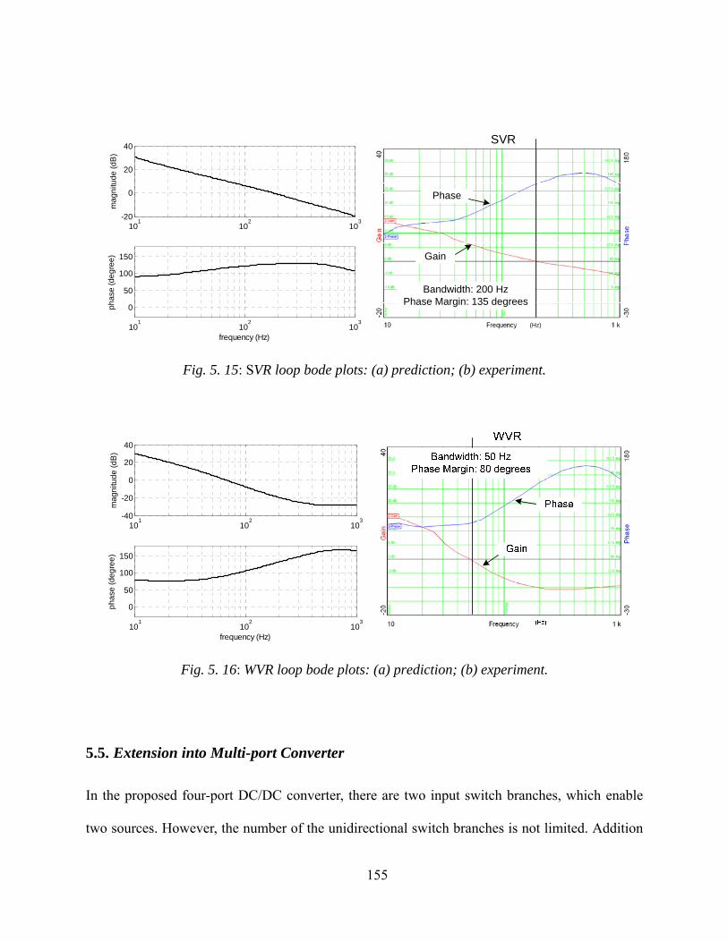
155
(Hz)
SVR
Bandwidth: 200 HzPhase Margin: 135 degrees
Gain
Phase
101
102
103
-20
0
20
40
mag
nitu
de (d
B)
101
102
103
0
50
100
150
frequency (Hz)
phas
e (d
egre
e)
Fig. 5. 15: SVR loop bode plots: (a) prediction; (b) experiment.
101
102
103-40
-20
0
20
40
mag
nitu
de (d
B)
101
102
103
0
50
100
150
frequency (Hz)
phas
e (d
egre
e)
Fig. 5. 16: WVR loop bode plots: (a) prediction; (b) experiment.
5.5. Extension into Multi-port Converter
In the proposed four-port DC/DC converter, there are two input switch branches, which enable
two sources. However, the number of the unidirectional switch branches is not limited. Addition
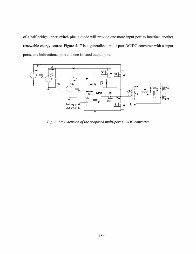
156
of a half-bridge upper switch plus a diode will provide one more input port to interface another
renewable energy source. Figure 5.17 is a generalized multi-port DC/DC converter with n input
ports, one bidirectional port and one isolated output port.
Fig. 5. 17: Extension of the proposed multi-port DC/DC converter

157
CHAPTER 6: CONCLUSIONS AND FUTURE WORK
This dissertation discusses the design and implementation of an integrated multi-port converter
solution for the satellite platform power system and the hybrid sources renewable system. A
general modeling procedure is proposed to derive the multi-port converter model. Various
control aspects like system control structure, MPPT, battery charging, etc, are discussed to
achieve the power management control. The interesting topic of current sharing for multi-port
converters is also introduced. Finally, a multi-port converter topology based on traditional half-
bridge converter is proposed to interface various renewable sources while maintaining a
regulated output voltage.
6.1. Major Contributions
The major contributions in this dissertation are summarized as follows.
1. A modeling procedure is proposed to derive the small signal model of the multi-port
converter. The modeling is based on state-space averaging method. Various modes of operation
have to be defined first, and then the state variables should be carefully chosen to reveal the
different ports’ dynamic characteristics. Control loops are cross coupled with each other due to
the power stage integration issue, therefore proper decoupling method is proposed to allow a
separate controller for each power port. Close loop controller design guidance is provided based
on the requirement of each power port’s characteristics.
2. The modular structure and the current sharing control strategy is proposed to achieve
operation of paralleled three-port converters, with MPPT for the solar port, battery charging

158
control for the battery port and bus regulation for the output port. A dual loop current sharing
control structure is identified to be suitable for multi-port converters, because of the convenient
decoupling feature of its current sharing loop and voltage regulation loop. Then, a hybrid current
sharing control structure which takes advantage of both active and passive current sharing
methods is proposed to avoid the drawback of current sharing bus in the active current sharing
method while achieving better dynamics than the passive method.
3. The system level control strategy is proposed to achieve the multi-objective power
management control goals. For this control strategy, the maximum power harvesting of the
renewable sources like solar array or wind turbine will be guaranteed under different conditions
of battery state of charge and load profiles. The control strategy is not only suitable for single
three-port converters, but also can be extended to be applying for multiple three-port channels,
with each channel one of the distributed units.
4. A four-port half-bridge topology is proposed for hybrid renewable sources with a battery
backup. The topology features low component count and ZVS for all main switches. One
isolation port is naturally available due to the half-bridge transformer. Modification based on the
traditional half-bridge topology makes it convenient for the practicing engineers to follow the
power stage design. The circuit operation of this converter and its control system is
experimentally verified. For the hybrid PV wind system, the proposed control structure is able to
achieve maximum power harvesting for PV and/or wind power sources, meanwhile maintaining
a regulated output voltage. Although the proposed four-port converter only has two input ports, it
can be extended to have n input ports.

159
6.2. Future Work
The promising results presented here warrant future investigation. Suggested future work is as
follows:
1. Derivation of more topologies for different applications. This half-bridge based
topology is suitable for low to medium power applications, while full-bridge based
multi-port converters will be more suitable for relatively high power applications.
2. For this half-bridge based multi-port converter, the soft switching range can still be
improved to allow higher frequency designs to further reduce the converter size. The
high side switch may lose ZVS when the battery is charging. Introducing some soft-
switching cells to the topology may solve this problem.
3. The modular design of the multi-port converter is an interesting topic. When multi-
port converters are paralleled together, it is very challenging to design the active
current sharing controllers since there are so many control loops coupled with each
other. It is very difficult to analyze and decouple the control loops, especially
considering the power stage non-identities. Therefore, a clear and easy to follow
design procedure is required to guide the design of paralleled multi-port converters.
4. The standard power interface or Power Electronics Building Blocks (PEBB) is a
promising concept, because a configurable “on-the-fly” converter can be told its
operating parameters and its function via software, can be useful in many applications
and offers the potential for a standardized interface. Based on PEBB concept, two
three-port converters can form a four-port or five-port converter depending on how
many ports of the three-port converter are connected together. Therefore, the

160
standardization and miniaturization of the multi-port converter is much desired. At
least for the proposed half-bridge converter prototype, a planar transformer can be
used to lower the board height since the transformer is the highest component. And
light load efficiency can be significantly improved by using some advanced
techniques like mode hopping and pulse skipping.
5. The control strategy still can be enhanced in many aspects. Proposed battery charging
algorithm includes two controllers, the constant current controller and the constant
voltage controller. Pre-charging and float-charging stages may also be included to
better condition the battery and extend its service lifespan. Additionally, an algorithm
suitable for various types of battery chemistries is desired. For the four-port converter,
only one mode of operation is discussed, while the other modes of operation still
needs specific consideration in various conditions like when only one of the
renewable sources is available or one MPPT function has to be disabled because of
limited load demanding.
161
REFERENCES
[1] A. Capel, “The power system of the multimedia constellation satellite for the Skybridge
Missions,” in Proc. IEEE Power Electronics Specialists Conf., 1998, pp. 1913-1930.
[2] H.W. Brandhorst, M.J. O'Neill, M. Eskenazi, “Photovoltaic options for increased satellite
power at lower cost,” in Proc. IEEE Photovoltaic Energy Conversion, 2003, pp. 849 -
852.
[3] S. Jang, J. Choi, “Energy balance analysis of small satellite in Low Earth Orbit (LEO),”
in Proc. IEEE Power and Energy Conference, 2008, pp. 967 - 971.
[4] R. D. Middlebrook and S. Cuk, “A General Unified Approach to Modeling Switching-
Converter Power Stages,” International Journal of Electronics, vol. 42, pp.521 - 550, June
1977.
[5] S. Cuk, “Modeling, Analysis, and Design of Switching Converters,” Ph.D. thesis,
California Institute of Technology, November 1976.
[6] A. Di Napoli, F. Crescimbini, L. Solero, F. Caricchi and F.G. Capponi, “Multiple-input
DC-DC Power Converter for Power-flow Management in Hybrid Vehicles,” in Proc.
IEEE Industry Application Conf., 2002, pp. 1578 - 1585.
[7] W. Jiang, B. Fahimi, “Multi-port Power Electric Interface for Renewable Energy
Sources,” in IEEE 2009 Applied Power Electronics Conference, 2009, pp.347-352.
[8] W. G. Imes, and F. D. Rodriguez, “A Two-Input Tri-State Converter for Spacecraft
Power Conditioning,” in Proc. AIAA International Energy Conversion Engineering
Conf., 1994, pp. 163 - 168.
162
[9] F. D. Rodriguez, and W. G. Imes, “Analysis and Modeling of A Two-Input DC/DC
Converter with Two Controlled Variables and Four Switched Networks,” in Proc. AIAA
International Energy Conversion Engineering Conf., 1994, pp. 322 - 327.
[10] B. G. Dobbs, and P. L. Chapman, “A Multiple-Input DC-DC Converter Topology, ” in
IEEE Power Electronics Letters, vol. 1, pp. 6-9, March 2003.
[11] N. D. Benavides, and P. L. Chapman, “Power Budgeting of a Multiple-Input Buck-Boost
Converter, ” IEEE Trans. Power Electronics, vol. 20, pp. 1303-1309, November 2005.
[12] H. Matsuo, W. Lin, F. Kurokawa, T. Shigemizu and N. Watanabe, “Characteristics of the
Multiple-Input DC–DC Converter, ” IEEE Trans. Industrial Applications, vol. 51, pp.
625 - 631, June 2004.
[13] L. Solero, F. Caricchi, F. Crescimbini, O. Honorati, and F. Mezzetti, “Performance of A
10 kW Power Electronic Interface for Combined Wind/PV Isolated Generating Systems,”
in Proc. IEEE Power Electronics Specialists Conf., 1996, pp. 1027-1032.
[14] L. Solero, A. Lidozzi, and J.A. Pomilio, “Design of Multiple-Input Power Converter for
Hybrid Vehicles,” in Proc. IEEE Applied Power Electronics Conf., 2004, pp. 1145 -
1151.
[15] Gui-jia Su, and F.Z. Peng, “A Low Cost, Triple-Voltage Bus DC-DC Converter for
Automotive Applications,” in Proc. IEEE Applied Power Electronics Conf., 2005,
pp.1015 - 1021.
[16] F. Z. Peng, H. Li, G. J. Su and J. S. Lawler, “A New ZVS Bidirectional dc-dc Converter
for Fuel Cell and Battery Applications, ” IEEE Trans. Power Electronics, vol. 19, pp. 54-
65, January 2004.
163
[17] H. Tao, A. Kotsopoulos, J.L. Duarte, M.A.M Hendrix, “Multi-Input Bidirectional DC-DC
Converter Combining DC-link and Magnetic-coupling for Fuel Cell Systems,” in Proc.
IEEE Industry Applications Conf., 2005, pp. 2021- 2028.
[18] Y. M. Chen, Y. C. Liu, and F. Y. Wu, “Multi-input DC/DC Converter Based On the
Multiwinding Transformer for Renewable Energy Applications, ” IEEE Trans. Industrial
Applications, vol. 38, pp. 1096 - 1104, August 2002.
[19] M. Michon, J.L. Duarte, M. Hendrix, and M.G. Simoes, “A Three-Port Bi-directional
Converter for Hybrid Fuel Cell Systems,” Proc. IEEE Power Electronics Specialists
Conf., 2004, pp. 4736 - 4742.
[20] H. Matsuo, W. Lin, F. Kurokawa, T. Shigemizu, and N. Watanabe, “Characteristic of the
Multiple-Input DC-DC Converter,” IEEE Trans. Industrial Electronics, 2004, vol. 51, pp.
625 - 631.
[21] H. Al-Atrash, F. Tian, I. Batarseh, “Tri-Modal Half-Bridge Converter Topology for
Three-Port Interface,” IEEE Trans. Power Electronics, vol. 22, pp. 341 - 345, January
2007.
[22] Z. Qian, O. Abdel-Rahman, J. Reese, H. Al-Atrash, I. Batarseh, “Dynamic Analysis of
Three-Port DC/DC Converter for Space Applications,” in Proc. IEEE Applied Power
Electronics Conf., 2009, pp.28 - 34.
[23] D. Liu, H. Li, “A ZVS Bi-Directional DC-DC Converter for Multiple Energy Storage
Elements,” IEEE Trans. Power Electronics, vol. 21, pp. 1513 - 1517, September 2006.
164
[24] C. Zhao, S.D. Round and J.W. Kolar, “An Isolated Three-Port Bidirectional DC-DC
Converter with Decoupled Power Flow Management,” IEEE Trans. Power Electronics,
vol. 21, pp. 2443 - 2453, September 2008.
[25] H. Tao, A. Kotsopoulos, J. L. Duarte and M. A. M. Hendrix, “Transformer-Coupled
Multiport ZVS Bidirectional DC–DC Converter With Wide Input Range, ” IEEE
Trans. Power Electronics, vol. 23, pp.771 - 781, March 2008.
[26] J. L. Duarte, M. Hendrix, and M. G. Simoes, “Three-Port Bidirectional Converter for
Hybrid Fuel Cell Systems, ” IEEE Trans. Power Electronics, vol. 22, pp.480 - 487,
March 2007.
[27] H. Al-Atrash, and I. Batarseh, “Boost-Integrated Phase-Shift Full-Bridge Converters for
Three-Port Interface,” in Proc. IEEE Power Electronics Specialists Conf., 2007, pp. 2313
- 2321.
[28] H. Al-Atrash, M. Pepper, and I. Batarseh, “A Zero-Voltage Switching Three-Port
Isolated Full-Bridge Converter,” in Proc. IEEE International Telecommunications Energy
Conf., 2006, pp. 411- 418.
[29] H. Tao; A. Kotsopoulos; J.L. Duarte; M.A.M., Hendrix, “Family of Multiport
Bidirectional DC-DC Converters,” in Proc. IEEE Power Electronics Specialists Conf.,
2008, pp. 796 - 801.
[30] J. A. Abu-qahouq; H. Mao; H. J. Al-atrash; I. Batarseh, “Maximum Efficiency Point
Tracking (MEPT) Method and Digital Dead Time Control Implementation,” IEEE
Trans. Power Electronics, vol. 21, pp. 1273 - 1281, September 2006.

165
[31] H. Li; D. Liu; F. Peng; G. Su, “Small Signal Analysis of A Dual Half Bridge Isolated
ZVS Bi-directional DC-DC converter for Electrical Vehicle Applications,” in Proc.
IEEE Power Electronics Specialists Conf., 2005, pp. 2777 - 2782.
[32] H. Al-Atrash; I. Batarseh, “Digital Controller Design for A Practicing Power Electronics
Engineer,” in Proc. IEEE Applied Power Electronics Conf., 2007, pp. 34 - 41.
[33] H. Mao; J. Abu-Qahouq; S. Luo; I. Batarseh, “Zero-Voltage-Switching Half-bridge DC-
DC Converter with Modified PWM Control Method,” IEEE Trans. Power Electronics,
vol. 19, pp.947 - 958, July 2004.
[34] D. P. Hohm; M. E. Ropp, “Comparative Study of Maximum Power Point Tracking
Algorithms Using An Experimental, Programmable, Maximum Power Point Tracking
Test Bed,” in Proc. IEEE Photovoltaic Specialists Conf., 2000, pp. 1699 - 1702.
[35] W. Wu, N. Pongratananukul, W. Qiu, K. Rustom, T. Kasparis, and I. Batarseh, “DSP-
based Multiple Peak Power Tracking for Expandable Power System,” in Proc. IEEE
Applied Power Electronics Conf., 2003, pp.525 - 530.
[36] R. W. Erickson and D. Maksimovic, Fundamentals of Power Electronics, 2nd edition.
Boston, MA: Kluwer, 2000, Chap. 7.
[37] D. C. Hamill, “Generalized Small-signal Dynamical Modeling of Multi-Port DC-DC
Converters,” in Proc. IEEE Power Electronics Specialists Conf., 1997, pp. 421 - 427.
[38] H. Al-Atrash, I. Batarseh, K. Rustom, “Statistical Modeling of DSP-based Hill-climbing
MPPT Algorithms in Noisy Environments,” in Proc. IEEE Applied Power Electronics
Conf., 2005, pp.1773 - 1777.
166
[39] Y. Liu, and Y. M. Chen, “A Systematic Approach to Synthesizing Multi-Input DC–DC
Converters,” IEEE Trans. Power Electronics, vol. 24, pp. 116 - 127, January 2009.
[40] A. Khaligh, J. Cao and Y. Lee, “A Multiple-Input DC–DC Converter Topology,” IEEE
Trans. Power Electronics, vol. 24, pp. 862 - 868, March 2009.
[41] A. Kwasinski, “Identification of Feasible Topologies for Multiple-Input DC-DC
Converters,” IEEE Trans. Power Electronics, vol. 24, pp. 856 - 861, March 2009.
[42] G. Su, and L. Tang, “A Reduced-Part, Triple-Voltage DC-DC Converter for EV/HEV
Power Management,” IEEE Trans. Power Electronics, vol. 24, pp. 2406 - 2410, October
2009.
[43] H. Tao, J.L. Duarte, M.A.M Hendrix, “Three-Port Triple-Half-Bridge Bidirectional
Converter With Zero-Voltage Switching,” IEEE Trans. Power Electronics, vol. 23, pp.
782 - 792, March 2008.
[44] Z. Qian, O. Abdel-Rahman, M. Pepper, I. Batarseh, “Analysis and Design for Paralleled
Three-port DC/DC Converters with Democratic Current Sharing Control,” in Proc. IEEE
Energy Conversion Congress and Exposition, 2009, pp. 1375-1382.
[45] R. W. Erickson and D. Maksimovic, Fundamentals of Power Electronics, 2nd edition.
Boston, MA: Kluwer, 2000, Chap. 7.
[46] H. Mao; J. Abu-Qahouq; S. Luo; I. Batarseh, “Zero-Voltage-Switching Half-bridge DC-
DC Converter with Modified PWM Control Method,” IEEE Trans. Power Electronics,
vol. 19, pp. 947 - 958, July 2004.
167
[47] Y. Panov, J. Rajagopalan and F.C. Lee, “Analysis and Design of N Parallel DC-DC
Converters with Master-Slave Current-Sharing Control,” in Proc. IEEE Applied Power
Electronics Conf., 1997, pp. 436-442.
[48] J. Sun, Y. Qiu, B. Lu, M. Xu, F.C. Lee, W.C. Tipton, “Dynamic Performance Analysis of
Outer-loop Current Sharing Control for Paralleled DC-DC Converters,” in Proc. IEEE
Applied Power Electronics Conf., 2005, pp. 1346 - 1352.
[49] W. Wu, N. Pongratananukul, W. Qiu, K. Rustom, T. Kasparis, I. Batarseh, “DSP-based
multiple peak power tracking for expandable power system,” in Proc. IEEE Applied
Power Electronics Conf., 2003, pp. 525-530.
[50] Y. Panov and M.M. Jovanovic, “Stability and Dynamic Performance of Current-Sharing
Control for Paralleled Voltage Regulator Modules,” IEEE Trans. Power Electronics, vol.
17, pp. 172-179, March 2002.
[51] Y. Zhang, R. Zane and D. Maksimovic, “System Modeling and Digital Control in
Modular Masterless Multi-phase DC-DC Converters,” in Proc. IEEE Power Electronics
Specialists Conf., 2006, pp.1-7.
[52] Y. Zhang, R. Zane, D. Maksimovic, “Current Sharing in Digitally Controlled Masterless
Multi-phase DC-DC Converters,” in Proc. IEEE Power Electronics Specialists Conf.,
2005, pp. 2722-2728.
[53] S. Luo, Z. Ye, R. Lin and F.C Lee, “A Classification and Evaluation of Paralleling
Methods for Power Supply Modules,” in Proc. IEEE Power Electronics Specialists Conf.,
1999, pp.901-908.
168
[54] K. Yao, M. Xu, Y. Meng, F.C. Lee, “Design Considerations for VRM Transient
Response Based on the Output Impedance,” IEEE Trans. Power Electronics, vol.18, pp.
1270-1277, November 2003.
[55] B.T. Irving and M.M. Jovanovic, “Analysis, Design, and Performance Evaluation of
Droop Current-Sharing Method,” in Proc. IEEE Applied Power Electronics Conf., 2000,
pp.235-241.
[56] I. Batarseh, K. Siri, H. Lee, “Investigation of the Output Droop Characteristics of
Parallel-connected DC-DC Converters,” in Proc. IEEE Power Electronics Specialists
Conf., 1994, pp. 1342-1351.
[57] R.B. Ridley, B.H. Cho, F.C. Lee, “Analysis and Interpretation of Loop Gains of
Multiloop-Controlled Switching Regulators,” IEEE Trans. Power Electronics, vol. 3, pp.
489-498, October 1988.
[58] Z. Qian, O. Abdel-Rahman, I. Batarseh, “An Integrated Four-Port DC/DC Converter for
Renewable Energy Applications,” accepted by IEEE Transactions on Power Electronics.
[59] Z. Qian, O. Abdel-Rahman, H. Al-Atrash, I. Batarseh, “Modeling and Control of Three-
Port DC/DC Converter Interface for Satellite Applications,” accepted by IEEE
Transactions on Power Electronics.
[60] Z. Qian, O. Abdel-Rahman, H. Hu, I. Batarseh, “Multi-channel Three-port DC/DC
Converters as Maximal Power Tracker, Battery Charger and Bus Regulator,” in Proc.
IEEE Applied Power Electronics Conference, 2010, pp. 2073-2079 .