Embed Size (px)
Citation preview
Abstract—Jitter happens when data rates increase in high-
speed input and output connections for data communications.
Characterizing of jitter and measurement is challenge, jitter
defined as the misalignment of edges in a sequence of data bits
from their ideal positions. Misalignments can result in data
errors, and raised bit error rate in digital communication.
Tracking these errors over an extended period determines the
system stability. Jitter can be due to deterministic and random
phenomena, also referred to as systematic and non-systematic
respectively. It is worth mentioning that the benefit of jitter is
limited to applications using random number generation.
There is hardly any other benefit from jitter. Phase noise and
jitter are a very important issue when design a phase-locked
and delay-locked loops. Different applications may have
different emphasis on the jitter specifications. “Cycle-to-cycle”
jitter refers to the time difference between two consecutive
Cycles of a period signal. A RMS (root mean square) or peak-
to-peak value is used to describe a random jitter. According to
the noise sources, it can be classified as internal jitters, caused
by the building blocks of PLLs and DLLs, and external jitters.
Jitters in an Oscillator have been examined for almost half a
century and still a hot topic.
Index Terms—Modelling and simulation, phase-locked loop,
PLL, frequency synthesizer, jitter noise, phase noise,
synchronization in digital transmission.
I. INTRODUCTION
ITTER happens when data rates increase in high-speed
input and output connections for data communications.
Characterizing jitter is a challenge, as is its measurement.
Jitter defined as the misalignment of edges in a sequence of
data bits from their ideal positions [1]. Misalignments can
result in data errors, and raised bit error rate in digital
communication. Tracking these errors over an extended
period determines the system stability. Jitter can be due to
deterministic and random phenomena [11], also referred to
as systematic and non-systematic respectively [2]. It is
worth mentioning that the benefit of jitter is limited to
applications using random number generation. There is
hardly any other benefit from jitter. Hence, the
disadvantages of jitter highly outweigh its benefits.
Timing jitter is of great concern in high frequency timing
circuits. Its presence can degrade the system performance in
many high-speed applications [3]. This paper describes the
relation between phase noise and jitter in high speed
communication as shown in fig .1 the real measurements of
Manuscript received March 11, 2017; revised April 1, 2017. This work
supported in part by the Research Center of Collage of Engineering, King
Saud University. Ahmed. A Telba is with King Saud University, Electrical
Engineering Department, P.O. Box 800, Riyadh 11421, Saudi Arabia, E-
mail: [email protected].
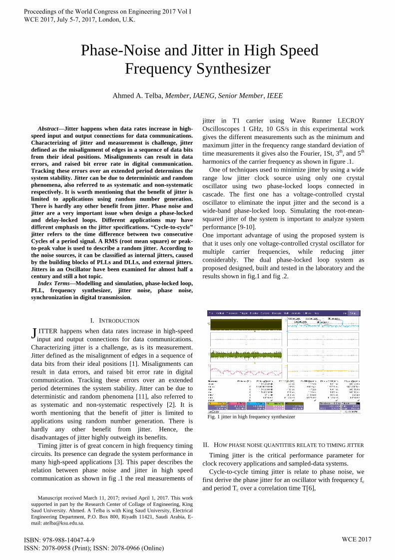
jitter in T1 carrier using Wave Runner LECROY
Oscilloscopes 1 GHz, 10 GS/s in this experimental work
gives the different measurements such as the minimum and
maximum jitter in the frequency range standard deviation of
time measurements it gives also the Fourier, 1St, 3th, and 5th
harmonics of the carrier frequency as shown in figure .1.
One of techniques used to minimize jitter by using a wide
range low jitter clock source using only one crystal
oscillator using two phase-locked loops connected in
cascade. The first one has a voltage-controlled crystal
oscillator to eliminate the input jitter and the second is a
wide-band phase-locked loop. Simulating the root-mean-
squared jitter of the system is important to analyze system
performance [9-10].
One important advantage of using the proposed system is
that it uses only one voltage-controlled crystal oscillator for
multiple carrier frequencies, while reducing jitter
considerably. The dual phase-locked loop system as
proposed designed, built and tested in the laboratory and the
results shown in fig.1 and fig .2.
II. HOW PHASE NOISE QUANTITIES RELATE TO TIMING JITTER
Timing jitter is the critical performance parameter for
clock recovery applications and sampled-data systems.
Cycle-to-cycle timing jitter is relate to phase noise, we
first derive the phase jitter for an oscillator with frequency fc
and period Tc over a correlation time T[6],
Phase-Noise and Jitter in High Speed
Frequency Synthesizer
Ahmed A. Telba, Member, IAENG, Senior Member, IEEE
J
Fig. 1 jitter in high frequency synthesizer
Proceedings of the World Congress on Engineering 2017 Vol I WCE 2017, July 5-7, 2017, London, U.K.
ISBN: 978-988-14047-4-9 ISSN: 2078-0958 (Print); ISSN: 2078-0966 (Online)
WCE 2017
dfT/sinfS4
dfe1fP2
TR0R2
tTtE
2
T/2j
22
(1)
From the integrand in (1), it is apparent that the close-in
phase noise near the carrier is significantly attenuated for
frequencies much smaller than T-1. We can gain further
insight by assuming a given shape for the phase spectral
density. Consider an oscillator with a constant phase noise
spectrum for frequencies f < f1 and zero everywhere else.
Then,
T2
Tf2sinfL4
dfT/sinL8
111
f
o
21
2 1
(2)
Where L1 is related to the value of in-band phase noise.
A free-running oscillator phase noise spectrum has a
region where L(f) (f)-2. Hence, we can model the noise
as white, frequency modulated (FM) noise as described in
[7],
2f
KfL
(3)
Where
K = L(f1) ((f1)2
(4)
Therefore,
fd
f
fTsin4
fdfTsinfL4
2
22
(5)
Using Parseval's relation, the integral can be evaluated as
Tf2fLTK42
1122
(6)
Relating the variance in phase to timing jitter,
T
f
ffL
f2
2
c
112
c
2
2T
(7)
The result has been derived in reference [8].
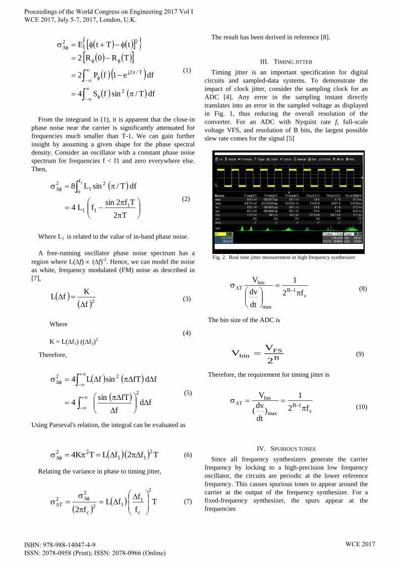
III. TIMING JITTER
Timing jitter is an important specification for digital
circuits and sampled-data systems. To demonstrate the
impact of clock jitter, consider the sampling clock for an
ADC [4]. Any error in the sampling instant directly
translates into an error in the sampled voltage as displayed
in Fig. 1, thus reducing the overall resolution of the
converter. For an ADC with Nyquist rate fs full-scale
voltage VFS, and resolution of B bits, the largest possible
slew rate comes for the signal [5]
c1B
max
binT
f2
1
dt
dv
V
(8)
The bin size of the ADC is
B
FSbin
2
VV (9)
Therefore, the requirement for timing jitter is
s1B
max
binT
f2
1
)dt
dv(
V
(10)
IV. SPURIOUS TONES
Since all frequency synthesizers generate the carrier
frequency by locking to a high-precision low frequency
oscillator, the circuits are periodic at the lower reference
frequency. This causes spurious tones to appear around the
carrier at the output of the frequency synthesizer. For a
fixed-frequency synthesizer, the spurs appear at the
frequencies
Fig. 2. Real time jitter measurement in high frequency synthesizer
Proceedings of the World Congress on Engineering 2017 Vol I WCE 2017, July 5-7, 2017, London, U.K.
ISBN: 978-988-14047-4-9 ISSN: 2078-0958 (Print); ISSN: 2078-0966 (Online)
WCE 2017
fspur = fc fref, fc 2 fref, fc 3 fref, ……, (11)
Spurs can present a problem because any interferer
located at a multiple of fref away from the desired signal will
fall directly in band after mixing. This is especially a
problem in cellular systems because the power of the
received signal from other users is often several orders of
magnitude larger than the desired signal. The location of the
other channels is precisely where the spurious tones from
the frequency synthesizer lie.
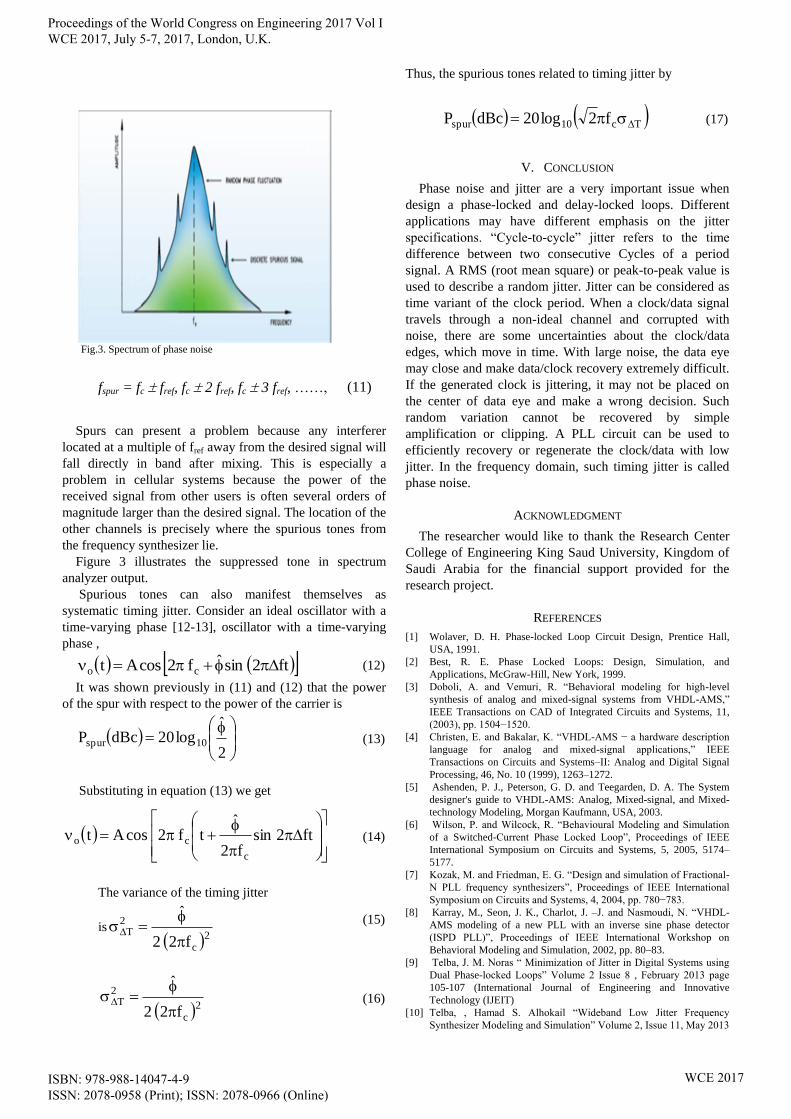
Figure 3 illustrates the suppressed tone in spectrum
analyzer output.
Spurious tones can also manifest themselves as
systematic timing jitter. Consider an ideal oscillator with a
time-varying phase [12-13], oscillator with a time-varying
phase ,
ft2sinˆf2cosAt co
(12)
It was shown previously in (11) and (12) that the power
of the spur with respect to the power of the carrier is
2
ˆlog20dBcP 10spur
(13)
Substituting in equation (13) we get
ft2sin
f2
ˆtf2cosAt
c
co (14)
The variance of the timing jitter
is
2c
2T
f22
ˆ
(15)
2c
2T
f22
ˆ
(16)
Thus, the spurious tones related to timing jitter by
Tc10spur f2log20dBcP (17)
V. CONCLUSION
Phase noise and jitter are a very important issue when
design a phase-locked and delay-locked loops. Different
applications may have different emphasis on the jitter
specifications. “Cycle-to-cycle” jitter refers to the time
difference between two consecutive Cycles of a period
signal. A RMS (root mean square) or peak-to-peak value is
used to describe a random jitter. Jitter can be considered as
time variant of the clock period. When a clock/data signal
travels through a non-ideal channel and corrupted with
noise, there are some uncertainties about the clock/data
edges, which move in time. With large noise, the data eye
may close and make data/clock recovery extremely difficult.
If the generated clock is jittering, it may not be placed on
the center of data eye and make a wrong decision. Such
random variation cannot be recovered by simple
amplification or clipping. A PLL circuit can be used to
efficiently recovery or regenerate the clock/data with low
jitter. In the frequency domain, such timing jitter is called
phase noise.
ACKNOWLEDGMENT
The researcher would like to thank the Research Center
College of Engineering King Saud University, Kingdom of
Saudi Arabia for the financial support provided for the
research project.
REFERENCES
[1] Wolaver, D. H. Phase-locked Loop Circuit Design, Prentice Hall,
USA, 1991.
[2] Best, R. E. Phase Locked Loops: Design, Simulation, and
Applications, McGraw-Hill, New York, 1999.
[3] Doboli, A. and Vemuri, R. “Behavioral modeling for high-level
synthesis of analog and mixed-signal systems from VHDL-AMS,”
IEEE Transactions on CAD of Integrated Circuits and Systems, 11,
(2003), pp. 1504−1520.
[4] Christen, E. and Bakalar, K. “VHDL-AMS − a hardware description
language for analog and mixed-signal applications,” IEEE
Transactions on Circuits and Systems–II: Analog and Digital Signal
Processing, 46, No. 10 (1999), 1263–1272.
[5] Ashenden, P. J., Peterson, G. D. and Teegarden, D. A. The System
designer's guide to VHDL-AMS: Analog, Mixed-signal, and Mixed-
technology Modeling, Morgan Kaufmann, USA, 2003.
[6] Wilson, P. and Wilcock, R. “Behavioural Modeling and Simulation
of a Switched-Current Phase Locked Loop”, Proceedings of IEEE
International Symposium on Circuits and Systems, 5, 2005, 5174–
5177.
[7] Kozak, M. and Friedman, E. G. “Design and simulation of Fractional-
N PLL frequency synthesizers”, Proceedings of IEEE International
Symposium on Circuits and Systems, 4, 2004, pp. 780−783.
[8] Karray, M., Seon, J. K., Charlot, J. –J. and Nasmoudi, N. “VHDL-
AMS modeling of a new PLL with an inverse sine phase detector
(ISPD PLL)”, Proceedings of IEEE International Workshop on
Behavioral Modeling and Simulation, 2002, pp. 80–83.
[9] Telba, J. M. Noras “ Minimization of Jitter in Digital Systems using
Dual Phase-locked Loops” Volume 2 Issue 8 , February 2013 page
105-107 (International Journal of Engineering and Innovative
Technology (IJEIT)
[10] Telba, , Hamad S. Alhokail “Wideband Low Jitter Frequency
Synthesizer Modeling and Simulation” Volume 2, Issue 11, May 2013
Fig.3. Spectrum of phase noise
Proceedings of the World Congress on Engineering 2017 Vol I WCE 2017, July 5-7, 2017, London, U.K.
ISBN: 978-988-14047-4-9 ISSN: 2078-0958 (Print); ISSN: 2078-0966 (Online)
WCE 2017

page153_155” (International Journal of Engineering and Innovative
Technology (IJEIT))
[11] T. H. Hee and A. Hajimiri, “Oscillator Phase Noise: A Tutoria
,”IEEE J. Solid-State Circuits , vol. 35, no. 3, pp. 326-336.
[12] The Designer’s Guide Community (www.desingers-guide.org),
Noise in Mixers, Oscillators, Samplers, and Logic by J. Philips
and K. Kundert
[13] K. Kouznetsov and R. Meyer, “Phase noise in LC oscillators,”
IEEE J. Solid-State Circuits, vol. 35, no. 8, pp. 1244-1248, Aug.
2000.
BIOGRAPHY
Dr. Ahmed Telba received his PhD from School of Engineering, Design
and Technology, University of Bradford UK Electronics and
Telecommunications. Currently he is a postdoctoral research associate in
Electronics and Communications, Electrical Engineering Department
collage of Engineering, King Saud University Saudi Arabia. Research
interests include analogue circuit design, phase locked loop, jitter in digital
telecommunication networks, pizo actuator, pizo generation and FPGA
Proceedings of the World Congress on Engineering 2017 Vol I WCE 2017, July 5-7, 2017, London, U.K.
ISBN: 978-988-14047-4-9 ISSN: 2078-0958 (Print); ISSN: 2078-0966 (Online)
WCE 2017