Embed Size (px)
Citation preview

Air Force Institute of TechnologyAFIT Scholar
Theses and Dissertations Student Graduate Works
3-21-2013
Photoacoustic Detection of Terahertz Radiation forChemical Sensing and Imaging ApplicationsStjepan Blazevic
Follow this and additional works at: https://scholar.afit.edu/etd
Part of the Electromagnetics and Photonics Commons
This Thesis is brought to you for free and open access by the Student Graduate Works at AFIT Scholar. It has been accepted for inclusion in Theses andDissertations by an authorized administrator of AFIT Scholar. For more information, please contact [email protected].
Recommended CitationBlazevic, Stjepan, "Photoacoustic Detection of Terahertz Radiation for Chemical Sensing and Imaging Applications" (2013). Thesesand Dissertations. 855.https://scholar.afit.edu/etd/855
PHOTOACOUSTIC DETECTION OF TERAHERTZ RADIATION FOR CHEMICAL SENSING AND IMAGING APPLICATIONS
THESIS
Stjepan Blazevic, FLTLT, RAAF
AFIT-ENG-13-M-08
DEPARTMENT OF THE AIR FORCE
AIR UNIVERSITY
AIR FORCE INSTITUTE OF TECHNOLOGY
Wright-Patterson Air Force Base, Ohio
DISTRIBUTION STATEMENT A. APPROVED FOR PUBLIC RELEASE; DISTRIBUTION UNLIMITED

The views expressed in this thesis are those of the author and do not reflect the official policy or position of the United States Air Force, Department of Defense, or the United States Government. This material is declared a work of the U.S Government and is not subject to copyright protection in the United States.
AFIT-ENG-13-M-08
PHOTOACOUSTIC DETECTION OF TERAHERTZ RADIATION FOR CHEMICAL SENSING AND IMAGING
THESIS
Presented to the Faculty
Department of Electrical and Computer Engineering
Graduate School of Engineering and Management
Air Force Institute of Technology
Air University
Air Education and Training Command
In Partial Fulfillment of the Requirements for the
Degree of Master of Science in Electrical Engineering
Stjepan Blazevic, B. E. E.
FLTLT, RAAF
March 2013
DISTRIBUTION STATEMENT A.
APPROVED FOR PUBLIC RELEASE; DISTRIBUTION UNLIMITED

AFIT-ENG-13-M-08
PHOTOACOUSTIC DETECTION OF TERAHERTZ RADIATION FOR CHEMICAL
SENSING AND IMAGING
Stjepan Blazevic, B. E. E.
FLTLT, RAAF
Approved:
___________________________________ _____Mar 2013____ Ronald A. Coutu, Jr. Ph.D. (Chairman) Date ___________________________________ _____ Mar 2013_____ LaVern A. Starman, Ph.D. (Member) Date ___________________________________ _____Mar 2013_____ Ivan R. Medvedev, Ph.D. (Member) Date

Abstract
The main research objective is the development of photoacoustic sensor capable
of detecting weak terahertz (THz) electromagnetic radiation. The feasibility of THz
remote sensing is seen in the utilization of Microelectromechanical systems (MEMS)
cantilever-based sensor. The overall sensing functionality of the detector in development
is based on the photoacoustic spectroscopy and direct piezoelectric effect phenomena, as
a result of which significant part of investigation has been conducted in the area of
terahertz electromagnetic radiation detection. The main focus of this research work was
the detector analytical and Finite Element Method (FEM) simulation modeling, involving
necessary material properties investigations and adequate selections which were, beside
the sensors’ geometry considerations, heavily engaged in the device modeling. Five
different MEMS detector configurations have been analyzed and modeled as potential
THz photoacoustic sensing options: Three configurations of rectangular shape, single
piezoelectric layer cantilever-based sensors, Circular membrane sensing configuration
and Square membrane sensing configuration. Some level of disagreement was discovered
between the analytical and FEM simulated results, which has been analyzed and possible
reasons were established. The obtained results indicated that the Square membrane has
demonstrated the ability to respond effectively to any radiation level from the entire THz
photoacoustic range exhibiting high sensitivity and thus was selected as the best terahertz
photoacoustic sensing solution.

Table of Contents
Page
Abstract .............................................................................................................................. iii
Table of Contents ............................................................................................................... iv
List of Figures .................................................................................................................... vi
List of Tables .......................................................................................................................x
I. Introduction .....................................................................................................................1
1.1. General Issue ....................................................................................................1 1.2 Problem Statement ............................................................................................1 1.3 Research Focus .................................................................................................2 1.4 Preview .............................................................................................................4
II. Background .....................................................................................................................5
2.1 Chapter Overview .............................................................................................5 2.2 Terahertz Detection ..........................................................................................5 2.3 Beam Theory ....................................................................................................9
2.3.1 Introduction ...................................................................................................... 9 2.3.2 Derivation ....................................................................................................... 10
2.4 Piezoelectric Sensing ......................................................................................13 2.5 Piezoresistive Sensing ....................................................................................18 2.6 Piezoelectric vs Piezoresistive ........................................................................23 2.7 Piezoelectric Cantilever Analytical Model .....................................................25 2.8 Gaussian Statistics ..........................................................................................29 2.9 Kinetic Theory of Gases .................................................................................31 2.10 Detector Functionality ....................................................................................32 2.11 Device Fabrication ..........................................................................................34 2.12 Summary .........................................................................................................39
III. Modeling ......................................................................................................................40
3.1 Chapter Overview ...........................................................................................40 3.2 Analytical Modeling .......................................................................................41 3.3 FEM Modeling................................................................................................42 3.4 Photoacoustic Spectroscopy ...........................................................................45 3.5 The Estimation of Terahertz Photoacoustic Pressure Range ..........................50 3.6 Cantilever-Based Piezoelectric Sensor ...........................................................55 3.7 Membrane-Based Piezoelectric Sensor ..........................................................59

3.8 Stochastic Cantilever Modeling ......................................................................63 3.9 Summary .........................................................................................................71
IV. Results and Analysis ....................................................................................................72
4.1 Chapter Overview ...........................................................................................72 4.2 Rectangular piezoelectric cantilever beam – Configuration I ........................72
4.2.1 Theoretical Analysis ...................................................................................... 76 4.2.2 FEM Analysis ................................................................................................. 87 4.2.3 Results Summary and Comparisons ............................................................. 105
4.3 Rectangular piezoelectric cantilever beam – Configuration II .....................113 4.4 Cross tethers sensing configuration ..............................................................118 4.5 Circular membrane sensing configuration ....................................................125 4.6 Square membrane sensing configuration ......................................................132 4.7 Summary .......................................................................................................140
V. Conclusions and Recommendations ..........................................................................141
5.1 Conclusions...................................................................................................142 5.2 Recommendations .........................................................................................143 5.3 Contributions ................................................................................................144
Appendix A ......................................................................................................................146
A-1 THz Photoacoustic Cantilever Fabrication Procedures ................................146 A-2 Configuration I CoventorWare® Process Editor Fabrication Process .........154 A-3 List of material properties used in the analytical and FEM modeling ..........159
Appendix B ......................................................................................................................160
B-1 Cross Tethers CoventorWare® Process Editor Fabrication Process ............160 B-2 Cross tethers configuration modal analysis results .......................................165
Appendix C ......................................................................................................................168
C-1 Circular Membrane CoventorWare® Process Editor Fabrication Process ...168 C-2 Circular Membrane FEM Modal and Mises Stress analysis results .............171
Appendix D ......................................................................................................................176
D-1 Square Membrane CoventorWare® Process Editor Fabrication Process .....176 D-2 Square Membrane FEM results for 0.52 µm x 0.52 µm PZT transducers ...180
Bibliography ....................................................................................................................183

List of Figures
Page Figure 1. Diagram of physical principles of Photoacoustic Microscopy (PAM) and
Photothermal Beam Deflection (PBD) [4] .................................................................. 8
Figure 2. Piezoelectricity [7]............................................................................................. 14
Figure 3. Piezoresistance [7] ............................................................................................. 20
Figure 4. Piezoelectric cantilever [13] .............................................................................. 25
Figure 5. Signal generation from the laser to the cantilever ............................................. 33
Figure 6. Cantilever L-Edit design layouts ....................................................................... 35
Figure 7. L-Edit 3D cantilever cross section .................................................................... 36
Figure 8. Fabrication process (A-E) and 3-D model view of released cantilever (F) [19] 38
Figure 9. Image of piezoelectric cantilever sensor before backsides etch and HF device
layer release [19] ........................................................................................................ 39
Figure 10. Chamber setup with piezoelectric cantilever detector [19] ............................. 46
Figure 11. Variation in the magnitude of the second-harmonic C2H2 photoacoustic signal
at constant analyte concentration (0.5 %) and 1000 mbar with modulation frequency
[5] ............................................................................................................................... 48
Figure 12. Photoacoustic signal response as a function of sample pressure for the
cantilever cell for acetylene (C2H2) [5] .................................................................... 49
Figure 13 Photoacoustic cell ............................................................................................. 50
Figure 14. Piezoelectric photoacoustic cantilever detector [19] ....................................... 55
Figure 15. Four cantilevers sensing configuration ............................................................ 57
Figure 16. 3D solid model of cross tethers sensing configuration .................................... 58

Figure 17. 3D solid model of circular membrane with diameter of 6 mm ....................... 60
Figure 18. L-Edit D square membrane design layout ....................................................... 61
Figure 19. CoventorWare 3D solid model of square membrane ...................................... 62
Figure 20. Pressure loaded beam ...................................................................................... 63
Figure 21. Voltage generation as function of applied pressure on top of PZT beam ....... 64
Figure 22. PDF for V=0 for Pc > α (Pm – Pc) .................................................................... 67
Figure 23. PDF for V=0 for Pc > α (Pm – Pc) .................................................................... 68
Figure 24. Voltage PDF for Variance =1, and mean Pm = 0 ............................................. 69
Figure 25. Voltage PDF for Variance = 0, and mean Pm = 1 ........................................... 70
Figure 26. Approximated (Dirac) pressure PDF ............................................................... 70
Figure 27. Cantilever L-Edit cross-section ....................................................................... 73
Figure 28. CoventorWare 3D solid model cantilever configuration ................................. 74
Figure 29. Cantilever PZT charge distribution ................................................................. 78
Figure 30. Open circuit voltage V across PZT .................................................................. 79
Figure 31. Calculated cantilever voltage generation as function of thickness ratio B ...... 82
Figure 32. Cantilever PZT charge distribution (Different PZT thickness) ....................... 83
Figure 33. Open circuit voltage V across PZT (Different PZT thickness) ........................ 84
Figure 34. Meshed cantilever model for tm =5 μm, tp=2.7 μm metal and SiO2 of 0.1 μm 89
Figure 35. Typical cantilever FEM simulation results...................................................... 91
Figure 36. Mises stress distribution of piezoelectric cantilever ........................................ 92
Figure 37. FEM voltage across 100 nm PZT layer ........................................................... 93
Figure 38. FEM voltage across 1μm PZT layer ................................................................ 94
Figure 39. FEM cantilever voltage generation as function of thickness ratio B ............... 97
Figure 40. Resulting vibrating pattern and resonant frequencies for a load of 10 mPa ... 99
Figure 41. Generalized Displacements plots .................................................................. 101
Figure 42. Frequency response involving Modal Damping Coefficient of 0.1 .............. 103
Figure 43. Frequency response involving Modal Damping Coefficient of 0.05 ............ 103
Figure 44. Frequency response involving Modal Damping Coefficient of 0.01 ............ 104
Figure 45. Analytical and FEM cantilever response observed for maximum voltage
sensitivity thickness ratios B. .................................................................................. 106
Figure 46. Rectangular cantilever L-Edit design layout (Configuration II) ................... 114
Figure 47. 3D solid model of cross tethers sensing configuration .................................. 119
Figure 48. Manhattan bricks mesh model with mesh optimal density of x = 200 μm, ... 120
Figure 49. Mode 1 vibrating pattern with resonant frequency of 2013.2 Hz.................. 124
Figure 50. Sensor Generalized Displacement for Mode 1 .............................................. 125
Figure 51. Membrane 3D FEM mesh model .................................................................. 126
Figure 52. FEM simulation result of circular membrane for a pressure load of ............. 129
Figure 53. Enlarged FEM simulation result of circular membrane for a pressure load of
10 Pa ........................................................................................................................ 130
Figure 54. FEM 3D meshed model of the square membrane ......................................... 133
Figure 55. Resulting vibrating pattern and resonant frequencies for a load of 10 mPa . 137
Figure 56. Square membrane generalized displacements plot ........................................ 138
Figure 57. Mises stress distribution of a square membrane configuration ..................... 140
Figure 58. Cross tethers resulting vibrating pattern and associated resonant frequencies
for a load of 10 mPa ................................................................................................ 166
Figure 59. Cross Tethers Generalized Displacements plots ........................................... 167

Figure 60. Circular membrane resulting vibrating pattern and resonant frequencies for a
load of 5 Pa .............................................................................................................. 172
Figure 61. Circular Membrane Generalized Displacements plots .................................. 173
Figure 62. FEM model result of the deflection of a clamped circular membrane for 5 Pa
photoacoustic load. .................................................................................................. 174
Figure 63. Circular Membrane FEM Mises stress distribution for 5 Pa photoacoustic
pressure load ............................................................................................................ 175
Figure 64. FEM 3D meshed model of the square membrane (Extruded bricks, element
order parabolic, element size in planar direction 200, element size in extrude
direction 5) ............................................................................................................... 180
Figure 65. Square membrane deflection for 10mPa uniformly distributed pressure load
................................................................................................................................. 181
Figure 66. Mises stress distribution of a square membrane configuration involving 0.52
µm x 0.52 µm PZT transducers ............................................................................... 182

List of Tables
Page Table 1. Pressure change inside photoacoustic cell for various ε and Ps of 1 mW ........... 54
Table 2. Voltage distribution for tp=100 nm ..................................................................... 79
Table 3. Voltage distribution for tp = 500nm .................................................................... 80
Table 4. Voltage distribution for tp=1μm .......................................................................... 80
Table 5. Generated voltage across PZT layers for p=1Pa ................................................ 81
Table 6. Voltage distribution across PZT for p=1 Pa and various tm, tp configuration
combinations .............................................................................................................. 86
Table 7. Cantilever response to uniformly distributed pressure load of 1Pa .................... 88
Table 8. CW FEM voltage distribution for tp = 100nm ................................................... 94
Table 9. CW FEM distribution for tp =1μm ...................................................................... 95
Table 10. CW FEM distribution for tp =2.5μm ................................................................ 95
Table 11. CW FEM voltage across PZT layers for p=1Pa .............................................. 96
Table 12. MemMech generalized harmonic display table .............................................. 100
Table 13. FEM and calculated cantilever response for the maximum voltage sensitivity
ratios B ..................................................................................................................... 107
Table 14. Calculated and simulated cantilever deflection and voltage generation for
different PZT layer thickness and applied pressure of 1Pa ..................................... 109
Table 15. FEM voltage generation for full and reduced layers structure ....................... 111
Table 16. Calculated voltage response for maximum voltage sensitivity configuration
(B=1.96) for tm=5 μm and tp=2.55 μm in case of Configuration I and Configuration
II modeling (comparison) ........................................................................................ 116

Table 17. FEM simulated voltage response for maximum voltage sensitivity
configuration (B = 1.85) for tm = 5 μm and tp = 2.7 μm in case of Configuration I
and Configuration II modeling (comparison) .......................................................... 116
Table 18. Generated voltages for the cross tethers beam based sensing configuration .. 121
Table 19. Generated voltages across PZT for three different sensing configurations .... 122
Table 20. Calculated resonant frequencies for cross tethers beam configuration ........... 123
Table 21. Membrane deflection response to uniformly distributed pressure loads ........ 127
Table 22. Membrane deflections for maximum voltage sensitivity configuration (B=1.85)
for tm=5 μm and tp=2.7 μm ...................................................................................... 128
Table 23. Membrane deflections and corresponding voltage response in a case of reduced
thickness configuration (B=1.85) with tm=1.5 μm and tp=0.8 μm ........................... 131
Table 24. Generated voltages for the square membrane sensing configuration ............. 134
Table 25. Generated voltages across PZT for three different sensing configurations .... 135
Table 26. Cross Tethers Configuration FEM resonant frequencies results .................... 165
Table 27. Cross Tethers generalized harmonic display results ....................................... 165
Table 28. Circular membrane FEM natural resonant frequencies results ....................... 171
Table 29. Circular membrane generalized harmonic display results .............................. 171
Table 30. Generated voltages for the square membrane sensing configuration involving
PZT transducers of 0.3 µm x 0.3 µm and 0.52 µm x 0.52 µm ................................ 181
1
PHOTOACOUSTIC DETECTION OF TERAHERTZ RADIATION FOR CHEMICAL SENSING AND IMAGING
I. Introduction
1.1. General Issue
This chapter provides the motivational reasons for researching in the field of
terahertz photoacoustic sensing in the context of an enormously increased number of
detection applications and provides a general overview of the nature of work investigated
in this thesis.
This work is mainly based on the previously developed theoretical assumptions
and experimental techniques that have been widely used in the past for spectral detection
in solids and gasses. This study uses analytical, as well as Finite Element Method (FEM)
modeling and analysis to design and develop a novel photoacoustic detector responsive to
sub-millimeter/terahertz radiation. Moreover, in addition to mentioned modeling methods
the utilization of a micro-cantilever transducer using MEMS manufacturing is also
explored.
1.2 Problem Statement
The basis of terahertz (THz) radiation which distinguishes its spectral region from
others is manly described through its interactions with low-pressure gasses, interactions
with gasses near atmospheric pressure, and interactions with liquids and solids [1].
Majority of the successful applications of this spectral region have been arisen from its
interactions with low-pressure gasses [1]. Based on this the feasibility of terahertz

2
sensing has been seen in the utilization of the extremely sensitive detectors embedded
within low-pressure environment such is photoacoustic cell filled by appropriate gas
sample. The possible solution is a proposed MEMS cantilever-based sensor. The idea of
using the microcantilever as a sensor in various sensing application is not new at all but
its unique design, geometry, material choice and fabrication process make it different and
unique from application to application. The choice of using a cantilever as a sensing
element is based on the proven cantilever benefits, such as their small size, fast response,
high sensitivity, as well as their relatively easy fabrication and integration with
electronics. Furthermore and most importantly the cantilever sensitivity can be easily
adjusted by changing materials or beam dimensions. Based on these factors, the proposed
research aimed to develop a novel photoacoustic terahertz radiation detector. The novelty
of this work is the miniature size of the acoustic cell with the use of the fabricated MEMS
cantilever transducer.
In this work the analytical and FEM simulated and results of a number of different
cantilever configurations have been collected, analyzed, validated and compared with
each other in respect to the best sensing performance. The full potential of this sensing
capability will be discussed in detail, along with its limitations, performance deviations
and implementation feasibility.
1.3 Research Focus
The purpose of this research project was to investigate and develop a novel
photoacoustic detector responsive to sub-millimeter/terahertz radiation. The proposed
research activity assumed the utilization of a micro-cantilever transducer using MEMS

3
manufacturing as well as the design of an acoustic cell. As briefly described in the
previous introduction section the intended transducer sensing functionality is based on
photoacoustic spectroscopy and direct piezoelectric effect phenomena. Before attempting
to fabricate any of the piezoelectric cantilevers a number of things needed to happen.
First, a comprehensive research in the field of piezoelectricity and terahertz radiation
needed to be conducted. This was accomplished and will be presented in Chapter II.
Second, during the initial stage of the detector development the main focus was on the
cantilever analytical modeling including appropriate material investigations and its
selection for cantilever fabrication. Based on the analytical predictions and material
selection, several versions of the complete MEMS cantilever designs, L-Edit surface
modeling, and related CoventorWare design and testing simulations were performed. The
CoventorWare Finite Element Method (FEM) simulation tool has been used extensively
in some advanced cantilever multi-layer structures investigations and were conducted to
get an idea of how the cantilevers/membranes should respond to an applied terahertz
acoustic wave and to get an estimate of the cantilever/membrane sensitivity. Based on L-
Edit sensor surface modeling designs and fully developed device fabrication process,
developed configurations of micro-cantilever transducers are ready for fabrication and
laboratory testing. Analytical and simulated results of a number of different sensor’s
configurations have been collected, analyzed and compared among each configuration as
well as in respect with design specifications. In each case the effect of variations in
models’ geometrical dimensions and impact of materials electromechanical properties on
sensing performance has been investigated and results will be presented and discussed to
define the best sensor design in terms of maximum voltage sensitivity.
4
1.4 Preview
This research is presented in five chapters. Chapter I introduces the problem,
reveals motivational reasons for researching in the field of terahertz photoacoustic
sensing and through the problem statement clearly identifies the main research objective.
The Research Focus section sets boundaries and specifies project execution order.
Chapter II presents the background theory in support of understanding the
research work presented in later chapters. In particular, special emphasis is given to the
basic terahertz photoacoustic sensing principles including a brief overview of the
importance of the THz frequency band for the future terahertz based applications.
Furthermore, the basics of beam theory, piezoelectric cantilever analytical model,
Gaussian statistics, and the basis of kinetic theory of gasses including detector fabrication
process description and its overall functionality as an integral terahertz detection device,
have been discussed and presented.
Chapter III discusses the key aspects involved in the modeling of piezoelectric
THz photoacoustic detectors with an accent on analytical and Finite Element Method
(FEM) modeling. In support, topics, such are Photoacoustic Spectroscopy and Kinetic
Theory of Gases as integral parts of the modeling process have been covered accordingly.
In addition, a theoretical illustration of stochastic cantilever modeling has been presented.
Chapter IV discusses, evaluates, and compares the sensing performance of each
proposed terahertz sensing configuration, modeled during this research work. In
particular after the description of the analytical and the simulated detectors conditions,
the results of the three cantilever-based and two so called membrane-based sensing

5
configurations have been analyzed in order to define the best sensor design in terms of
maximum voltage sensitivity.
Chapter V provides conclusion and suggestions for future work. The results in
Chapter IV and contributions stated in Chapter V reflect the overall research success.
II. Background
2.1 Chapter Overview
This chapter summarizes the foundations upon which this work was built. First,
the basis of terahertz electromagnetic radiation detection has been discussed and
presented accordingly. Secondly, the theoretical background on the topics, such are beam
theory, piezoelectric and piezoresistive sensing including comparison between two
sensing principles are introduced and key points highlighted. Furthermore, the
piezoelectric cantilever analytical model, the brief introduction of the basis of Gaussian
statistics and its role in the statistical analysis of physical phenomena has been presented,
too. Lastly, the basis of kinetic theory of gasses and the detector’s overall functionality as
a sensor and its fabrication process are described.
2.2 Terahertz Detection
In order to be able to monitor and control a vast number of physical processes,
mechanical motions, material testing or microscopic imaging including monitoring of air
pollutants there is an increased need to find and develop new methods and instruments
capable of providing accurate measurements of acoustic waves properties. In this thesis

6
section, the physical basis of photoacoustic detection as well as the nature of terahertz
radiation in general and its potential practical use in future applications have been
discussed. This section provides a brief background on the generation of terahertz
radiation, its detection with an accent on the photoacoustic sensing principles, as well as
the increased importance of this frequency band including current and future terahertz
based applications.
Terahertz radiation refers to the electromagnetic waves radiation in the frequency
range between 300GHz and 3000GHz, or between 0.3 THz and 3 THz with
corresponding wavelength ranging from 0.1mm (infrared) to 1 mm (microwave). Some
authors refer to the THz band simply as sub-millimeter radiation, or even as
tremendously high frequency. The terahertz frequency band is known as the least
explored portion of the electromagnetic spectrum, mainly due to the initial difficulties of
generating and detecting radiation at these frequencies [1]. However, according to D.
Mittleman “It is no longer problem in the THz radiation production and its sensing so,
researches are able to concentrate more on what to do with this radiation, and less on how
to produce it [2].” These days, market demands for commercial use of terahertz sensors
and sources have had a rapid increase and there is an indication that further progress in
some areas without development of terahertz technology (mainly instrumentations) is
practically impossible. It is obvious that recent availability of reliable sources in a variety
of THz ranges will have a wide impact on science and industry. New terahertz
applications such are imagining through materials, fog or dust; point and remote gas
detection; detection of prohibited and dangerous substances or pharmaceutical

7
applications [3] are some examples that will find their practical use in a number of
different areas.
Since the photoacoustic effect was investigated and discovered by A.G. Bell in
the late 1800s, it has not attracted particular attention until the development of lasers
and very sensitive detection techniques [4]. During that time this effect has been
mainly utilized in instrumentation development where relevant gas measurements have
been required. The photoacoustic effect is based on the conversion of light energy into
sound energy by a gas, liquid or solid. The energy conversion occurs when light is
absorbed by molecules causing their rotation at a higher energy level. An increase in
vibration will result in local heating (temperature increase) and a certain increase in
pressure. The modulated pressure will result in an acoustic wave, which can be
detected with an appropriate measuring device, such as a microphone or a cantilever
(photoacoustic membrane). The intensity of the acoustic wave greatly depends on the
geometry of the gas cell, the intensity of the incident electromagnetic wave and
absorption coefficient of the sample gas [5]. There are a number of theoretical models
for the generation and detection of photoacoustic signals; however, for the purpose of
this thesis a brief illustration of a model involving piezoelectric detection is shown in
Figure 1.

8
Figure 1. Diagram of physical principles of Photoacoustic Microscopy (PAM) and Photothermal Beam Deflection (PBD) [4] When an electromagnetic wave (probe beam) is absorbed by a solid (e.g.
semiconductor), certain amount of light energy is converted into local heat causing
thermal wave propagation through a solid sample [4]. As the thermal wave propagation
intensity increases it can be then detected by a piezoelectric transducer attached directly
to the sample. Besides the piezoelectric there are a number of other methods and
techniques that can be used for signal detection and its measurements. Most common, but
not limited to are Optical Beam Deflection (OBD), Photo Radiometry (PTR),
Microphone gas-cell detection, Photoacoustic Microscopy (PAM), Photothermal Beam
Deflection (PBD) [4], etc. However, majority if not all them emphasize the contribution
of the optical and thermal parameters to the acoustic signal generation. Thus, generation
of photoacoustic signal is basically a three step process consisting of optical energy
absorption, followed by generation and propagation of thermal energy, and detection of
modulated thermal radiation by a piezoelectric transducer or any other appropriate

9
pressure sensitive measuring device. Without going further into a comprehensive
explanation of the photoacoustic phenomena just a final remark that firm grasp of the
acoustic response is becoming essential for the future THz wave detection applications.
Due to the fact that terahertz radiation is capable of penetrating through a wide
variety of non-polar and non-conducting (non-metallic) materials [6] such as fabrics,
plastics, paper, wood or ceramics including even penetration through fog and clouds, the
development of wide range of THz sources and detectors capable of measuring both
broad-band and narrow-band signals are going to find their application in areas such as
communications, security, biomedical and scientific use of imaging, quality control and
process monitoring, etc. Also, the unique property of the acoustic waves which is a low
attenuation in the air due to its moisture will enable remote THz spectroscopy as well as
THz wave sensing using acoustic waves in remote operation.
2.3 Beam Theory
2.3.1 Introduction
Beam deflection is essentially a displacement caused by a loading condition.
When designing a beam, deflection is generally undesired. Critical factor in beams design
is its stiffness which is defined as the ability of the beam to resist deflection or simply
based on materials elastic properties is the ability of a material to resist deformation.
Deflection is described analytically by the Euler-Bernoulli equation [7] that serves as a
governing equation in solving MEMS related problems. The two key assumptions in the
Euler-Bernoulli beam theory are that the material is linear elastic (Hooke’s law) and that

10
cross sections of the beam remain planar and perpendicular to the neutral axis during
bending [7].
2.3.2 Derivation
The static Euler-Bernoulli beam equation is a result of a combined relationship
between the kinematic, constitutive, force resultant, and equilibrium equations. The
resulting outcome of this relationship is briefly summarized within this sub-section.
Kinematics, in accordance with linear beam theory basically describes the amount the
created strain in the beam as function of deflection taking into account the amount of
each beam’s cross-sectional point movement in the length direction [7]. For a small
deflection there is negligible strain in the y direction and consequently the neutral plane
does not change in length. The beam bends towards the neutral plane with arc of
curvature χ, rotation angle Ѳ, and beams’ displacement ԝ. The beams’ cross section
rotation is expressed as the negative slope of displacement w.
𝜒 = −Ѳ = − 𝑑𝑤𝑑𝑥
(1)
For approximately linear materials the relationship between stress σ and strain ε within
the beam is described by the constitutive equation employing Hooke’s law [7].
σx = 𝐸 ∙ εx (2)

11
Beam theory usually uses the 1- dimensional Hooke’s law (2), however, the stress
and strain are functions of entire beam cross-section and then they can vary with y as
indicated in the following equation (3)
𝜎(𝑥, 𝑦) = 𝐸 ∙ 𝜀(𝑥, 𝑦) (3)
where σ is the stress, ε is the strain, and E is the Young’s Modulus.
Furthermore, the force resultant equations in the mentioned combined relationship
are used to describe the direct and shear stress in a beam as a function of x and y. The
equations integrate the individual, small moments M and shear stresses V over entire
beams’ cross-sectional area.
𝑀(𝑥) = ∬ 𝑦 ∙ 𝜎 (𝑥, 𝑦) ∙ 𝑑𝑦 ∙ 𝑑𝑧 (4)
𝑉(𝑥) = ∬ 𝜎𝑥𝑦 (𝑥, 𝑦) ∙ 𝑑𝑦 ∙ 𝑑𝑧 (5)
Last equations involved in the relationship which form Euler-Bernoulli beam
equation are the equilibrium equations. These equations relate the beam’s external
pressure loads with its internal stresses. The equilibrium in this relation is established by
equating the change in shear force to pressure load p and change in moment to shear
force resultant for each small section of the beam.
𝑑𝑉𝑑𝑥
= 𝑝 (6)

12
𝑑𝑀𝑑𝑥
= −𝑉 (7)
Furthermore, substituting equation (6) into equation (7) will provide the
relationship between the bending moment M, the distributed load p and axial force N.
Then the substitution of the obtained relationship into following equation
𝐸𝐼 𝑑²𝑦𝑑𝑥²
= 𝑀 (8)
which relates the applied bending moment M and the curvature will give us equation
known as Euler-Bernoulli beam equation.
𝑑²𝑑𝑥²
�𝐸𝐼 𝑑2𝑤𝑑𝑥2 � = 𝑝(𝑥) (9)
where EI is the flexural rigidity or bending modulus [7].
Considering this fourth order differential equation, each successive equation’s
derivative of the deflection has a unique physical interpretation. The first derivative with
respect to the length represents the angle between the beam and neutral axis. The second
and third derivatives are the net moment and shear force on the beam respectively, while
the fourth derivative is a net load per unit length. Using boundary conditions and
balancing derivative terms in equation to desired static or dynamic forcing will determine
the beam operational model. Different set of boundary conditions will result in different
solutions of beams equation determining its operation model. For example solving

13
equation with the set of boundary conditions 𝑦 = 0, 𝑑𝑦𝑑𝑥
= 0 at length 𝑥 = 0 will define
one end fixed beam configuration (cantilever) [7].
2.4 Piezoelectric Sensing
This section provides a brief background on the piezoelectricity as a physical
phenomenon in general with an accent on the piezoelectric sensing principles. By
definition, piezoelectricity is an electric charge (or voltage) generated in a material under
applied mechanical pressure (stress) [8]. Alternately, the materials change their physical
shapes when an electric field is applied to them. Both effects, widely known as direct and
inverse effect of piezoelectricity are result of the same fundamental property of the
crystal [8]. A basic understanding of the electromechanical coupling, which virtually
describes ability of piezoelectric material to convert mechanical energy into electrical,
and vice versa [9], is briefly explained through the electromechanical coupling
coefficient, usually denoted by a small letter k. If we apply a mechanical pressure to one
side of a single piezoelectric element, a fraction of the applied pressure will be converted
to an electric charge on the opposite element’s side. When the pressure is removed from
the element, the generated electric charge will disappear. This simplified physical
phenomenon can be easily stated by the following formula:
𝑘2 = 𝑚𝑒𝑐ℎ𝑎𝑛𝑖𝑐𝑎𝑙 𝑒𝑛𝑒𝑟𝑔𝑦 𝑐𝑜𝑛𝑣𝑒𝑟𝑡𝑒𝑑 𝑡𝑜 𝑒𝑙𝑒𝑐𝑡𝑟𝑖𝑐𝑎𝑙 𝑒𝑛𝑒𝑟𝑔𝑦
𝑎𝑝𝑝𝑙𝑖𝑒𝑑 𝑚𝑒𝑐ℎ𝑎𝑛𝑖𝑐𝑎𝑙 𝑒𝑛𝑒𝑟𝑔𝑦 [8]
This same basic relationship holds true in the case of inverse effect of piezoelectricity,

14
where change in element’s shape occurs when an electric field is applied to it. It is
expressed as:
𝑘2 = 𝑒𝑙𝑒𝑐𝑡𝑟𝑖𝑐𝑎𝑙 𝑒𝑛𝑒𝑟𝑔𝑦 𝑐𝑜𝑛𝑣𝑒𝑟𝑡𝑒𝑑 𝑡𝑜 𝑚𝑒𝑐ℎ𝑎𝑛𝑖𝑐𝑎𝑙 𝑒𝑛𝑒𝑟𝑔𝑦
𝑎𝑝𝑝𝑙𝑖𝑒𝑑 𝑒𝑙𝑒𝑐𝑡𝑟𝑖𝑐𝑎𝑙 𝑒𝑛𝑒𝑟𝑔𝑦 [8]
All of what has been said above can be easily summarized through the use of the
configuration shown in Figure 2 which is generally used in MEMS devices to illustrate
the piezoelectric effects.
Figure 2. Piezoelectricity [7]
15
In Figure 2a the thin piezoelectric film of length l, thickness t and width w is
sandwiched between two metal electrodes. When an input voltage Vi is applied across the
film as depicted in Figure 2b, the shape of the film is deformed. In a case when a force or
stress is applied to the film in Figure 2c, due to its capacitors’ role the film first generates
an electrical charge Q and then provides open circuit voltage Vo= 𝑄𝐶
as result of direct
piezoelectric effect. As long as force or stress remains constant or their acting on
piezoelectric element is removed after certain amount of time the generated electrical
charge Q will disappear as a result of its leakage through film resistance itself or an
outside resistance resulting in zero output voltage V0. This property of piezoelectric
materials is used for sensing purposes when dealing with time-varying signals [6] while
for actuating purposes the film works under AC as well as under DC voltage, as electrical
charge Q is supplied from a voltage source Vi [7].
Furthermore, analytical expressions which describe the direct and inverse effects
of piezoelectricity relating the electrical and mechanical properties of materials involved
in sensors’ structure are as shown in equations (10) and (11) respectively [9].
𝐷 = 𝜀𝑇𝐸 + 𝑑𝑇 (10)
𝑆 = 𝑑𝐸 + 𝑠𝐸𝑇 (11)
where D is the dielectric displacement, E is the electric field, T is the mechanical stress, S
is the mechanical strain, d is the transverse piezoelectric coefficient, ε is the permittivity

16
and s is the mechanical compliance. The subscript T means the piezoelectric material is
under constant stress, i.e. a mechanically free condition, and the subscript E means that it
is under constant electric field, i.e. a short-circuit condition [9].
The above piezoelectric constitutive equations can be rewritten using matrix
notation to represent the stress and strain relationship in vector notation [9].
⎣⎢⎢⎢⎢⎡𝑆1𝑆2𝑆3𝑆4𝑆5𝑆6⎦
⎥⎥⎥⎥⎤
=
⎣⎢⎢⎢⎢⎡
𝜀11𝜀22𝜀33
2𝜀232𝜀312𝜀12⎦
⎥⎥⎥⎥⎤
=
⎣⎢⎢⎢⎢⎡𝜀1𝜀2𝜀3𝜀4𝜀5𝜀6⎦
⎥⎥⎥⎥⎤
and
⎣⎢⎢⎢⎢⎡𝜎11𝜎22𝜎33𝜎23𝜎31𝜎12⎦
⎥⎥⎥⎥⎤
⎣⎢⎢⎢⎢⎡𝜎1𝜎2𝜎3𝜎4𝜎5𝜎6⎦
⎥⎥⎥⎥⎤
=
⎣⎢⎢⎢⎢⎡𝑇1𝑇2𝑇3𝑇4𝑇5𝑇6⎦
⎥⎥⎥⎥⎤
(12)
The subscripts 1, 2 and 3 correspond to the x-axis, y-axis and z-axis in the
Cartesian coordinate system respectively. In double subscripts notation such as for
example d31 the first subscript corresponds to the electrical term while the second to the
mechanical term. So, using matrix notation from above the piezoelectric constitutive
equations can be written in the following forms [9];
𝐷𝑖 = 𝜀𝑖𝑗𝑇𝐸𝑗 + 𝑑𝑖𝑗𝑇𝑗 (13)
𝑆𝑖 = 𝑑𝑖𝑗𝐸𝑗 + 𝑠𝑖𝑗𝐸𝑇𝑗 (14)
From presented it appears that there are several parameters that are used to
specify the electromechanical properties of piezoelectric materials. Besides the

17
electromechanical coupling factor k that was introduced at the beginning of this section
among important are dielectric constant K (relative permittivity), the elastic compliance s
and piezoelectric coefficient d. The elastic compliance s is defined as the strain produced
per unit stress while the dielectric constant is the ratio of the permittivity of the material
to that of vacuum (K = ε /εo). Among mentioned the piezoelectric coefficient d is the
parameter that more or less describe the piezoelectric material ability to convert the
mechanical stress in the electrical charge and consequently open circuit voltage across
piezoelectric element. The piezoelectric coefficient is a measure of generated charge Q in
response to external mechanical excitations such are moment M, tip force F or uniformly
distributed photoacoustic pressure load p. The piezoelectric transducer (sensor) typically
transduces the longitudinal stress as a polarization charge proportional to its transverse
piezoelectric coefficient, d. In general the piezoelectric coefficient d is defined [9] as the
electric polarization P, generated in a material per unit of mechanical stress T, i.e.
P = dT (15)
More detailed analytical approach which relates the electrical charge Q generation
to external mechanical excitations is presented in Section 2.7 which summarizes
piezoelectric cantilever analytical modeling.
In addition to all what has been said so far, before concluding this section just a
few final remarks related to the piezoelectric effect and piezoelectric sensing in general.
It turns out that the most important properties of the piezoelectric materials and their
ability to sense are coming from their crystal structures which have impact on energy

18
band gaps height and consequently a change in semiconductor resistivity. Therefore,
piezoelectric materials such are ceramics or certain types of single crystals (e.g. GaAs or
Quartz SiO2) are widely used for sensing and actuation purposes. In their applications the
direct effect is normally used for sensing technology, while the inverse effect is used for
actuating technology. Piezoelectric sensors have been widely proven as reliable and
versatile measurement tools in many industrial sensing applications. They have been
successfully used in areas, such are aerospace, medicine, nuclear instrumentation, process
control or for research and development purposes. Beside their well-known classic
applications such are microphones, acoustic modems or acoustic imaging for underwater
or underground objects and many others, now they have found their application in
MEMS technology too, mainly as a pressure, inertia, tactile or flow sensors. The rise of
piezoelectric technology is mainly driven by the piezoelectric materials’ native
characteristics. Their high modulus of elasticity enables the development of piezoelectric
sensing elements with almost zero deflection. This, in nature mechanical property makes
piezoelectric sensors rugged, with extremely high natural frequency and linearity over a
wide amplitude range. Piezoelectric technology is practically insensitive to
electromagnetic fields and radiation. Also, there are some practical piezoelectric
materials, which exhibit high temperature stability. So, all of these enables this type of
sensors to perform measurements under harsh environmental conditions.
2.5 Piezoresistive Sensing
In contrast to the piezoelectric effect, the piezoresistive effect does not produce
electrical charge (voltage) at all. The piezoresistive effect only causes a change in

19
electrical resistance. An electrical resistor will simply change its resistance due to the
applied mechanical stress. This effect is commonly used in the MEMS field for a wide
range of sensing applications [10]. A quite simple physical explanation and
understanding of piezoresistive effect can be efficiently summarized through the use of
general expression for piezoresistivity (16) and graphical illustration of piezorezistance
shown in Figure 3. The rectangular beam of length l, width w, and thickness t is stretched
by tensile force F while a voltage V is applied across beams’ length. Taking into account
geometrical dimensions and material resistivity the resistance value of the beam can be
calculated using the following resistance equation derived from Ohm’s law:
𝑅 = 𝜌𝑟𝑙𝐴
= 𝜌𝑟𝑙
𝑤𝑡 [7] (16)
where 𝜌𝑟 is the material’s resistivity.

20
Figure 3. Piezoresistance [7]
Considering the equation from above it can be clearly seen that the overall
resistance value as result of applied strain can be changed in a two main ways. First, the
resistors’ length and cross section will change with strain. An increase in length will
likely cause a decrease in resistors’ cross section and consequently an increase in
resistance as carriers that make current have to travel longer distance, while an increase
in cross-sectional area will result in resistance decrease, as carriers in this case can flow
in parallel. Secondly, the change in strain besides having an impact on resistors’
dimensions will cause the change in resistivity of certain materials. The magnitude of
resistance change through the change in bulk resistivity is much greater than in case
related to the change in resistors’ dimensions. Based on this fact piezoresistors are strictly
defined as resistors whose resistivity changes with applied strain [10]. The change in

21
resistance, caused only by the physical deformation of resistor is a unique property of
metals. In case of semiconductor materials, the mechanical force will not only have an
impact on the resistor’s geometry, but it will also cause a change in the internal crystal
structure by changing the atomic spacing. This type of change will have an impact on
energy band gaps and consequently a change in semiconductor resistivity. Will resistivity
in this case increase or decrease depends on the material type and strain. Different
materials have different energy gaps (smaller or larger), and then it is just a matter of
applied mechanical force to increase or decrease electrons’ (carrier charges) travel
distance and mobility (affected by the number of collisions per travel distance) on their
way to conduction band. Some deformation will simply decrease travel distance and
increase mobility, and make it easier for electrons to be raised into the conduction band,
having for result decreased resistivity while in some cases it is going to be the opposite,
where increased travel distance and decreased mobility will simply result in increased
resistivity. The dependence of resistivity of a semiconductor’ material on the mobility of
charge carriers is expressed by the following mobility formula [10]:
µ = qt˟m̽
(17)
where q is the charge per unit charge carrier, t˟ is mean free time between carrier
collision events, and m̽ is the effective mass of a carrier in the crystal lattice. So, it is
obvious that piezoresistivity has a much greater impact on resistance than just a simple
change in geometry. As a result of this simplified and brief analysis it can be seen that

22
semiconductors in their nature are much more sensitive to applied mechanical force, as
well as to the environmental conditions (e.g., temperature, light) than metals. The
piezoresistive effect in some most popular semiconductor materials, such are silicon
(polycrystalline, amorphous) or germanium can be several orders of magnitudes more
pronounced than the geometrical effect in metals. All these are making semiconductors
more suitable for a variety of sensing applications. There is a wide range of products
using piezoresistive effect. Due to its processing, electrical and a number of other
qualities, silicon is a material of greatest interest for use in the development and
fabrication of piezoresistive devices (e.g., pressure or acceleration sensors).
Furthermore, the transduction (sensing) principle for both detectors types
(piezoelectric and piezoresistive) is that external mechanical excitations (force F,
pressure p) applied at the bending mode element such is cantilever beam will cause
mechanical deformations inducing bending stress in the cantilever. The resulting stress
can be transformed into a measurable output signals by either the piezoelectric or
piezoresistive effect. Piezoelectric sensor, as mentioned in previous section typically
transduces the longitudinal stress as polarization charge proportional to its transverse
piezoelectric coefficient d31 while piezoresistor typically transduces the longitudinal
stress as a change in resistivity proportional to its longitudinal piezoresistive
coefficient 𝜋𝑙, which is defined as
𝜋𝑙 = 𝛥𝜌𝑟/𝜌𝑟𝜎𝑥
[7] (18)
23
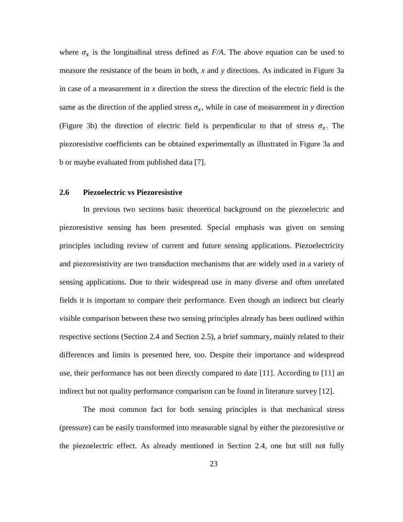
where 𝜎𝑥 is the longitudinal stress defined as F/A. The above equation can be used to
measure the resistance of the beam in both, x and y directions. As indicated in Figure 3a
in case of a measurement in x direction the stress the direction of the electric field is the
same as the direction of the applied stress 𝜎𝑥, while in case of measurement in y direction
(Figure 3b) the direction of electric field is perpendicular to that of stress 𝜎𝑥. The
piezoresistive coefficients can be obtained experimentally as illustrated in Figure 3a and
b or maybe evaluated from published data [7].
2.6 Piezoelectric vs Piezoresistive
In previous two sections basic theoretical background on the piezoelectric and
piezoresistive sensing has been presented. Special emphasis was given on sensing
principles including review of current and future sensing applications. Piezoelectricity
and piezoresistivity are two transduction mechanisms that are widely used in a variety of
sensing applications. Due to their widespread use in many diverse and often unrelated
fields it is important to compare their performance. Even though an indirect but clearly
visible comparison between these two sensing principles already has been outlined within
respective sections (Section 2.4 and Section 2.5), a brief summary, mainly related to their
differences and limits is presented here, too. Despite their importance and widespread
use, their performance has not been directly compared to date [11]. According to [11] an
indirect but not quality performance comparison can be found in literature survey [12].
The most common fact for both sensing principles is that mechanical stress
(pressure) can be easily transformed into measurable signal by either the piezoresistive or
the piezoelectric effect. As already mentioned in Section 2.4, one but still not fully

24
proven disadvantage of piezoelectric sensors is that they cannot be used for fully static
measurements. Based on the fact that pressure sensors use both piezoelectric and
piezoresistive operating principles, here is a brief advantage-disadvantage summary
between these two sensing principles. Piezoelectric pressure sensors have advantages
such as fast response, self-generating signal, and they are rugged, small in size and have a
wide temperature operating range, while their disadvantages are mainly related to low
sensitivity, they are greatly affected by environmental temperature changes, have high
output impedance, and they are vibration sensitive and responsive to AC signals only.
The main disadvantage of piezoresistive pressure sensors is their temperature sensitivity,
while they have several advantages such as DC response, high sensitivity, fast response
and small size. Also, as a general observation [11] in case of other sensing applications
such are piezoresistive and piezoelectric cantilevers, the piezoresistive cantilever has a
slight performance advantage, mainly due to its smaller low frequency noise. In power
constrained applications the performance of piezoresistive sensing greatly declines.
Based on the power dissipation observations, generally piezoresistive sensing
outperforms piezoelectric sensing in application where power dissipation is not an issue.
As a final remark to this comparison the piezoelectricity is in general preferred for
sensing within noisy ambient. This preference is based on the fact that piezoresistive
sensing has lower noise and lower sensitivity than piezoelectric sensing.
25
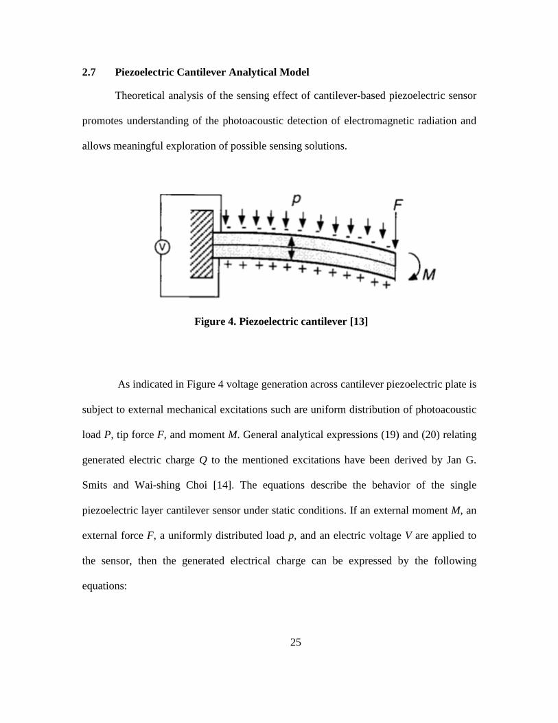
2.7 Piezoelectric Cantilever Analytical Model
Theoretical analysis of the sensing effect of cantilever-based piezoelectric sensor
promotes understanding of the photoacoustic detection of electromagnetic radiation and
allows meaningful exploration of possible sensing solutions.
Figure 4. Piezoelectric cantilever [13]
As indicated in Figure 4 voltage generation across cantilever piezoelectric plate is
subject to external mechanical excitations such are uniform distribution of photoacoustic
load P, tip force F, and moment M. General analytical expressions (19) and (20) relating
generated electric charge Q to the mentioned excitations have been derived by Jan G.
Smits and Wai-shing Choi [14]. The equations describe the behavior of the single
piezoelectric layer cantilever sensor under static conditions. If an external moment M, an
external force F, a uniformly distributed load p, and an electric voltage V are applied to
the sensor, then the generated electrical charge can be expressed by the following
equations:
26
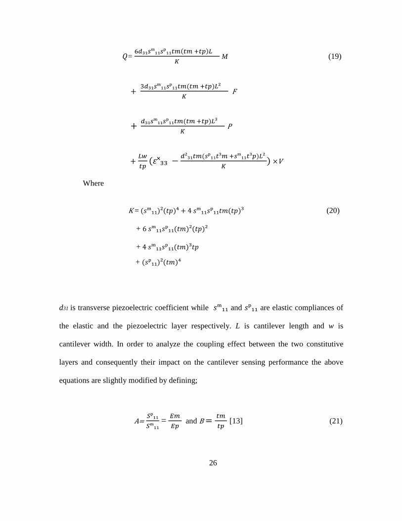
𝑄= 6𝑑₃₁𝑠ᵐ₁₁𝑠ᵖ₁₁𝑡𝑚(𝑡𝑚 +𝑡𝑝)𝐿 𝐾
M (19)
+ 3𝑑₃₁𝑠ᵐ₁₁𝑠ᵖ₁₁𝑡𝑚(𝑡𝑚 +𝑡𝑝)𝐿²
𝐾 F
+ 𝑑₃₁𝑠ᵐ₁₁𝑠ᵖ₁₁𝑡𝑚(𝑡𝑚 +𝑡𝑝)𝐿³ 𝐾
P
+ 𝐿𝑤𝑡𝑝
(𝜀˟₃₃ − 𝑑²₃₁𝑡𝑚(𝑠ᵖ₁₁𝑡³𝑚 +𝑠ᵐ₁₁𝑡³𝑝)𝐿² 𝐾
) ×V Where K = (𝑠ᵐ₁₁)²(𝑡𝑝)⁴ + 4 𝑠ᵐ₁₁𝑠ᵖ₁₁𝑡𝑚(𝑡𝑝)³ (20) + 6 𝑠ᵐ₁₁𝑠ᵖ₁₁(𝑡𝑚)²(𝑡𝑝)² + 4 𝑠ᵐ₁₁𝑠ᵖ₁₁(𝑡𝑚)³𝑡𝑝 + (𝑠ᵖ₁₁)²(𝑡𝑚)⁴
d31 is transverse piezoelectric coefficient while 𝑠ᵐ₁₁ and 𝑠ᵖ₁₁ are elastic compliances of
the elastic and the piezoelectric layer respectively. L is cantilever length and w is
cantilever width. In order to analyze the coupling effect between the two constitutive
layers and consequently their impact on the cantilever sensing performance the above
equations are slightly modified by defining;
A= 𝑆ᵖ₁₁𝑆ᵐ₁₁
= 𝐸𝑚 𝐸𝑝
and B = 𝑡𝑚 𝑡𝑝
[13] (21)

27
where Em and Ep are Young’s modulus of elastic and piezoelectric layers respectively.
Substituting (21) into (19) will give
𝑄 = 6𝑑₃₁𝐿 𝑡²𝑝
𝐴𝐵(𝐵 +1) 1+4𝐴𝐵+6𝐴𝐵²+4𝐴𝐵³+𝐴²𝐵⁴
×M (22)
+ 3𝑑₃₁𝐿² 𝑡²𝑝
𝐴𝐵(𝐵 +1) 1+4𝐴𝐵+6𝐴𝐵²+4𝐴𝐵³+𝐴²𝐵⁴
× 𝐹
+ 𝑑₃₁𝐿³𝑤 𝑡²𝑝
𝐴𝐵(𝐵 +1) 1+4𝐴𝐵+6𝐴𝐵²+4𝐴𝐵³+𝐴²𝐵⁴
× 𝑝
+ 𝐿𝑤𝜀˟₃₃ 𝑡𝑝
(1- 𝑘²₃₁ 𝐴𝐵(1+𝐴𝐵³) 1+4𝐴𝐵+6𝐴𝐵²+4𝐴𝐵³+𝐴²𝐵⁴
) ×V
The cantilever capacitance between bottom side of the top metal plate and top side of the
bottom metal plate is
C = 𝐿𝑤𝜀˟₃₃ 𝑡𝑝
× (1-k²31 𝐴𝐵�1+𝐴𝐵³�
1+4𝐴𝐵+6𝐴𝐵²+4𝐴𝐵³+𝐴²𝐵⁴) [15] (23)
where ε˟₃₃= ε0K˟₃ is the dielectric constant of the piezoelectric material under a free
condition and 𝑘²₃₁ is the transverse piezoelectric coupling coefficient. From the
modified constitutive equation (22) when only external load p (uniformly distributed

28
pressure, acoustic signal) is applied the total electric charge generated at piezoelectric
plate is
𝑄 = 𝑑₃₁𝐿³𝑤 𝑡²𝑝
𝐴𝐵(𝐵 +1) 1+4𝐴𝐵+6𝐴𝐵²+4𝐴𝐵³+𝐴²𝐵⁴
×p
+ 𝐿𝑤𝜀˟₃₃
𝑡𝑝 (1- 𝑘²₃₁ 𝐴𝐵(1+𝐴𝐵³)
1+4𝐴𝐵+6𝐴𝐵²+4𝐴𝐵³+𝐴²𝐵⁴ ) ×V (24)
As by definition voltage V = 𝑄
𝐶 , dividing equation (24) by equation (23) will give us
the total open circuit electric voltage generated across cantilever piezoelectric plate
(transducer), i.e.
V = 𝑑₃₁𝐿²𝜀˟₃₃𝑡𝑝
× 𝐴𝐵(𝐵+1)
1+4𝐴𝐵+6𝐴𝐵²+4𝐴𝐵³+𝐴2𝐵4−𝑘²₃₁ 𝐴𝐵(1+𝐴𝐵3)× 𝑝 (25)
Furthermore, above generated voltage can also be related to the tip displacement
by following equation
V = 3𝑑₃₁ 𝑡²𝑝
4𝜀˟₃₃ 𝑆𝐷₁₁𝐿² × 𝐴𝐵(𝐵+1)
𝑅−𝑘²₃₁ 𝐴𝐵(1+𝐴𝐵3) ×
𝑅𝐴𝐵+1
𝛿 [13] (26)

29
where 𝑆𝐷₁₁ = 1 𝐸𝑝
, δ is tip deflection and 𝑅 = 1 + 4𝐴𝐵 + 6𝐴𝐵² + 4𝐴𝐵³ + 𝐴2𝐵4. By
measuring the tip deflection the electric voltage generated on the piezoelectric cantilever
can be obtained from the above equation.
2.8 Gaussian Statistics
Gaussian statistics has an important role in the statistical analysis of physical
phenomena. This section provides only a brief review of Gaussian statistics in order to
support cantilever stochastic response analysis presented in Chapter III. The concept of
statistical problem modeling is based on definition and properties of Gaussian random
variables and Gaussian random process. A random variable U is called Gaussian (or
normal) if its characteristic function is given in the form
𝑀𝑈(𝜔) = 𝑒𝑥 𝑝 � 𝑗𝜔ū − 𝜔2𝜎2
2 � [11] (27)
Well-known Gaussian probability density functions (PDF) is defined as
𝑃𝑈(𝑢) = 1√2𝜋𝜎
𝑒𝑥 𝑝 � − (𝑢−ū)2𝜎2 � [11] (28)
The most important properties of random variable are its
mean value, ū = ∫ 𝑢 𝑃𝑈(𝑢) 𝑑𝑢∞−∞ , (29)

30
mean – square value, ū² = ∫ 𝑢² 𝑃𝑈(𝑢) 𝑑𝑢∞−∞ , (30)
variance, 𝜎² = ∫ (𝑢 − ū)² 𝑃𝑈(𝑢) 𝑑𝑢∞−∞ , (31)
and standard deviation 𝜎 = √𝜎2 (32)
The standard deviation describes dispersion of random variables around mean.
Random variables U₁, U₂, U₃, . . ., Un are called jointly Gaussian random variable if their
joint characteristic function is defined as
𝑀𝑈(ῳ) = 𝑒𝑥 𝑝 � 𝑗ū˟𝑡ῳ − 12
ῳ𝑡𝐶ῳ� (33)
where
ū˟= [ū₁; ū₂; ū₃, … , ū𝑛], ῳ = [ω₁; ω₂; ω₃, …,ωn]
and C is an n x n covariance matrix defined as the following expectation
𝜎²𝑖𝑘 = 𝐸[(𝑢𝑖 − ū𝑖)(𝑢𝑘 − ū𝑘)] (34)
Moreover, a random process U(t) is said to be a Gaussian random process if
random variables U(t₁), U(t₂), U(t₃),…,U( tk) are jointly Gaussian random variables for
given sets of times. Then for time instants t₁, t₂, t₃… tn the joint probability density
function is given in the form

31
𝑃𝑈(𝑢˟) = 1(2𝜋)𝑎𝑛/2𝐶1/2 𝑒𝑥 𝑝 � − 1
2 (𝑢˟ − ū˟)𝐶−1(𝑢˟ − ū˟) � (35)
where
u˟ = [u (t₁); u (t₂); u (t₃)…u (tn) and ū˟ = [ū (t₁); ū (t₂); u (t₃)… ū (tn)],
C is once again covariance matrix, with element 𝜎²𝑖𝑗 in the 𝑖𝑡ℎ row and 𝑗𝑡ℎ column
defined as
𝜎²𝑖𝑗 = 𝐸�𝑢(𝑡𝑖) − ū (𝑡𝑖) ] [𝑢�𝑡𝑗) − ū (𝑡𝑗� � (36)
As Gaussian random variables and random process are widely used in most
physics and engineering applications, there is enormously huge amount of literature
available elsewhere detailing their unique properties.
2.9 Kinetic Theory of Gases
Kinetic theory of gases will play an important role in the functionality of the
future terahertz photoacoustic detector. As an accurate model is essential to the function
of a sensor, before progressing with any model simulations the necessary estimation of
the THz photoacoustic pressure range needs to be determined first. In relation to that, this
section presents the Beer-Lambert and ideal gas laws that will be used in Chapter III to
estimate the pressure change inside the photoacoustic gas chamber as result of absorption
of energy from incoming terahertz radiation.
32
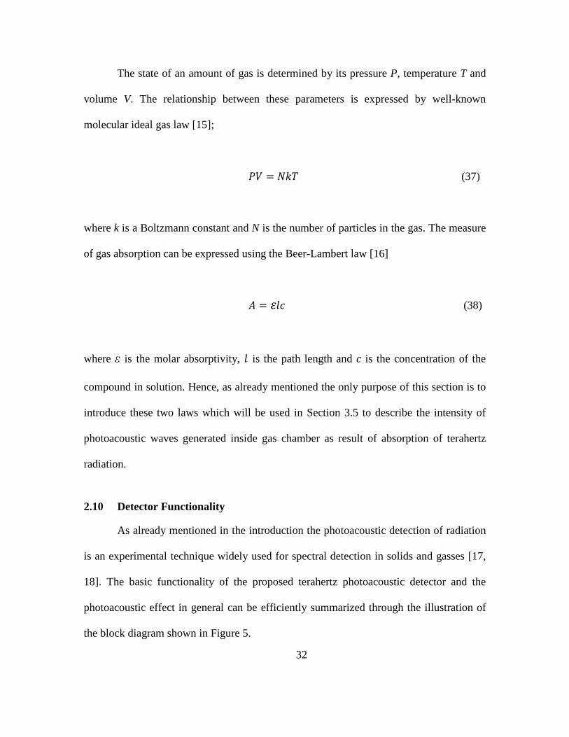
The state of an amount of gas is determined by its pressure P, temperature T and
volume V. The relationship between these parameters is expressed by well-known
molecular ideal gas law [15];
𝑃𝑉 = 𝑁𝑘𝑇 (37)
where k is a Boltzmann constant and N is the number of particles in the gas. The measure
of gas absorption can be expressed using the Beer-Lambert law [16]
𝐴 = 𝜀𝑙𝑐 (38)
where ε is the molar absorptivity, 𝑙 is the path length and c is the concentration of the
compound in solution. Hence, as already mentioned the only purpose of this section is to
introduce these two laws which will be used in Section 3.5 to describe the intensity of
photoacoustic waves generated inside gas chamber as result of absorption of terahertz
radiation.
2.10 Detector Functionality
As already mentioned in the introduction the photoacoustic detection of radiation
is an experimental technique widely used for spectral detection in solids and gasses [17,
18]. The basic functionality of the proposed terahertz photoacoustic detector and the
photoacoustic effect in general can be efficiently summarized through the illustration of
the block diagram shown in Figure 5.

33
Figure 5. Signal generation from the laser to the cantilever
As in the case of a number of different spectroscopy applications there is no
exception here, the generation of photoacoustic signal which is going to be detected by
cantilever will be initiated by a laser beam transmission towards target material (solids,
gasses, etc.). An optical source which is integral part of the detector emits terahertz
radiation. When the radiation beam is absorbed by the target sample due to molecular
collisions heat is generated in the material. The generated heat spreads inside material
increasing pressure in a space limited sample. Consequently as a result of the thermal
expansion, generated heat leaves material and in a region of the infrared or light beam
(thermal light) producing acoustic (pressure) wave. A photoacoustic sensor such as
cantilever is going to be used to detect this acoustic wave. The modulation of the
transmitted infrared beam with a desired THz modulation frequency will generate
acoustic signal with a frequency equal to that of the modulation. As the frequency
response of the micromachined cantilever depends on the amplitude of the pressure wave
generated by heating of the sample it is obvious that the choice of infrared modulation by
appropriate terahertz modulation frequency will determine the operation mode. The
cantilever can be simply described as a harmonic oscillator. So, choosing its resonant or
non-resonant frequency as a modulation frequency will determine the mode of operation.
The cantilever is usually used in non-resonant mode due to the better noise performance.

34
Furthermore, once terahertz photoacoustic signal has reached the top side of
piezoelectric cantilever will cause its bending and due to the direct piezoelectric effect
the electrical charge generation on the opposite cantilever side will occur. The resulting
cantilever deflection caused by the photoacoustic waves will be measured with optical
interferometers. It is important to keep the cantilever inside a well-sealed evacuated
photoacoustic chamber in order to avoid pressure broadening. Another equally important
reason to keep the photoacoustic cell internal pressure constant but below atmospheric
pressure (vacuum) is related to the photoacoustic spectroscopy detection requirements.
An increase in operating pressure inside the chamber will result in frequency broadened
photoacoustic signals. Conversely a decrease in the pressure will ensure a narrower
photoacoustic response and aid in the identification of signals within the frequency
spectrum for very closely spaced absorption lines.
2.11 Device Fabrication
The initial cantilever fabrication has been performed on a 100mm silicon-on-
insulator (SOI) wafer with <100> crystal orientation and overall thickness of 500µm. The
proposed beam geometry with optimal device and Lead Zirconate Titanate (PZT) layer
thickness ratio for maximum voltage sensitivity is intended to be used in the sensing
configuration shown in Figure 6. Fabrication process described in this section is related to
the mentioned cantilever configuration and as such due to the characteristic multi-layer
beam structure without major changes is applicable to all sensing configuration discussed
within this thesis document. Full step by step fabrication procedures can be also seen in
Appendix A. In general, established fabrication procedure consists of the following

35
fabrication steps; deposition of oxide layer, deposition of bottom contact metal,
deposition of PZT, deposition of top metal contact, backside etch, and removal of buried
oxide.
Figure 6. Cantilever L-Edit design layouts As depicted in Figure 7 the cantilever physical structure were comprised of three
thin films; a 1 μm thick PZT layer sandwiched between two metal contacts with
individual thickness of 0.1 μm. The thickness of a device layer is 5 μm while the
cantilever length and width are 5 mm and 2 mm respectively. To release the cantilever, a
hole was etched through the backside of the wafer and the buried oxide was removed
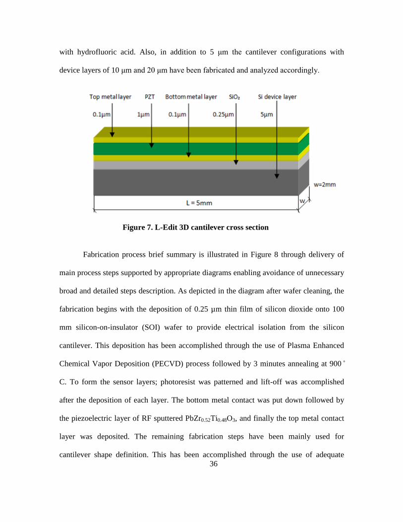
36
with hydrofluoric acid. Also, in addition to 5 μm the cantilever configurations with
device layers of 10 μm and 20 μm have been fabricated and analyzed accordingly.
Figure 7. L-Edit 3D cantilever cross section
Fabrication process brief summary is illustrated in Figure 8 through delivery of
main process steps supported by appropriate diagrams enabling avoidance of unnecessary
broad and detailed steps description. As depicted in the diagram after wafer cleaning, the
fabrication begins with the deposition of 0.25 µm thin film of silicon dioxide onto 100
mm silicon-on-insulator (SOI) wafer to provide electrical isolation from the silicon
cantilever. This deposition has been accomplished through the use of Plasma Enhanced
Chemical Vapor Deposition (PECVD) process followed by 3 minutes annealing at 900 ̊
C. To form the sensor layers; photoresist was patterned and lift-off was accomplished
after the deposition of each layer. The bottom metal contact was put down followed by
the piezoelectric layer of RF sputtered PbZr0.52Ti0.48O3, and finally the top metal contact
layer was deposited. The remaining fabrication steps have been mainly used for
cantilever shape definition. This has been accomplished through the use of adequate

37
etching solutions. As indicated in Figure 8 (diagram C) the buffered oxide etching (BOE)
has been used to etch patterned window in silicon dioxide layer followed by the Deep
reactive-ion etching (DRIE) of Si device layer. The precise etch stopping has been
provided by buried SiO2 layer. The final beam shaping has been accomplished through
the backside substrate etching using DRIE (diagram D) and cantilever release (diagram
E) by HF removal of buried oxide. After every single fabrication step the necessary
inspections, measurements and if required step repetition have been performed in order to
satisfy strict fabrication requirements. The 3D model of released cantilever and almost
fabricated cantilever device before its actual backside etch and HF device layer release is
shown in Figure 8 (F) and Figure 9, respectively. The laser interferometer has been used
to measure the cantilever deflection while the piezoelectric voltage signals are recorded
for identifying detector terahertz sensitivity.

38
Figure 8. Fabrication process (A-E) and 3-D model view of released cantilever (F) [19]

39
Figure 9. Image of piezoelectric cantilever sensor before backsides etch and HF device layer release [19]
2.12 Summary
This chapter outlined the foundation necessary to move forward in this area of
research. The required theoretical background and understanding of terahertz
electromagnetic radiation generation with an accent on its detection has been presented,
including piezoelectric cantilever analytical model, the basis of beam theory and the
importance of Euler-Bernoulli equation in solving MEMS related problems and the basis
of Gaussian statistics, which plays an important role in the statistical analysis of physical
phenomena. Moreover, the basis of kinetic theory of gasses with accent on Beer-Lambert
and ideal gas laws has been introduced, too. Furthermore, a basic background on the
piezoelectric and piezoresistive sensing has been presented with a special emphasis on
the comparison between these two sensing principles, including a brief performance
based analysis of some current sensing applications. Lastly, the overall functionality of

40
the proposed terahertz photoacoustic detector has been summarized and the detector
fabrication process is described step by step, and key points in its physical
implementation have been highlighted.
III. Modeling
3.1 Chapter Overview
This chapter presents a discussion of the key aspects involved in the modeling of
piezoelectric THz photoacoustic detectors. It covers topics, such as analytical and FEM
modeling method analysis of developed, single piezoelectric layer rectangular and
membrane shape sensor configurations. Furthermore, Photoacoustic Spectroscopy will be
presented as an intended method for detection of terahertz photoacoustic signals. Further
discussion will focus on Kinetic Theory of gasses with accent on Beer-Lambert and ideal
gas laws, which have been used in this research to describe the part of detectors’
functionality associated with photoacoustic cell, and to determine the expected
measurable terahertz photoacoustic pressure range inside the gas chamber. The final three
sections of this chapter will present the Cantilever-based Piezoelectric Sensor and the
Membrane-based Piezoelectric Sensor as main sensor configurations, developed in this
project including a theoretical illustration of stochastic piezoelectric cantilever modeling.

41
3.2 Analytical Modeling
Based on the analytical model for the single piezoelectric layer cantilever
presented in Section 2.7 and derived model equations [13] for the capacitance between
cantilevers’ top and bottom metal plates
C = 𝐿𝑤𝜀˟₃₃ 𝑡𝑝
× (1-k²31 𝐴𝐵�1+𝐴𝐵³�
1+4𝐴𝐵+6𝐴𝐵²+4𝐴𝐵³+𝐴²𝐵⁴), (23)
the generated electrical charge between top and bottom metal plates
𝑄 = 𝑑₃₁𝐿³𝑤 𝑡²𝑝
𝐴𝐵(𝐵 +1) 1+4𝐴𝐵+6𝐴𝐵²+4𝐴𝐵³+𝐴²𝐵⁴
×p
+ 𝐿𝑤𝜀˟₃₃
𝑡𝑝 (1- 𝑘²₃₁ 𝐴𝐵(1+𝐴𝐵³)
1+4𝐴𝐵+6𝐴𝐵²+4𝐴𝐵³+𝐴²𝐵⁴ ) ×V, (24)
and model equations relating generation of the open circuit voltage across cantilevers’
PZT element as functions of uniformly distributed photoacoustic load p
V = 𝑑₃₁𝐿²𝜀˟₃₃𝑡𝑝
× 𝐴𝐵(𝐵+1)
1+4𝐴𝐵+6𝐴𝐵²+4𝐴𝐵³+𝐴2𝐵4−𝑘²₃₁ 𝐴𝐵(1+𝐴𝐵3)× 𝑝 (25)
and cantilever deflection δ
42
V = 3𝑑₃₁ 𝑡²𝑝
4𝜀˟₃₃ 𝑆𝐷₁₁𝐿² × 𝐴𝐵(𝐵+1)
𝑅−𝑘²₃₁ 𝐴𝐵(1+𝐴𝐵3) ×
𝑅𝐴𝐵+1
𝛿 [13] (26)
comprehensive cantilever analysis for a wide range of thickness ratios B has been
conducted in order to determine the best beam configuration in terms of maximum
voltage sensitivity. During the modeling process, the device layer thickness 𝑡𝑚 has been
kept fixed while the thickness of the PZT layer 𝑡𝑝 has been continuously changed in
appropriate thickness increments until the thickness ratio B for maximum voltage
sensitivity has been observed. In respect to the cantilever configurations with variable 𝑡𝑝
and fixed device layer thickness of 𝑡𝑚 = 5μm and with 𝑡𝑝 ranging from 0.1μm up
to 𝑡𝑝=3.3μm with an increment rate of 100nm have been modeled and continuously
investigated for the entire terahertz photoacoustic pressure range. Moreover, besides
thickness ratios B, the configurations with different geometrical dimensions including
cantilevers’ length, width and PZT coverage area have been modeled and investigated
accordingly. Full investigation process and obtained results analysis of each cantilever
based developed sensing option is presented in relevant sections of Chapter IV.
Furthermore, analytical modeling of circular membrane configuration has not been
developed and its sensing performance analysis is based on performed FEM modeling.
3.3 FEM Modeling
In theory, finite element method (FEM) which is generally used in the MEMS
design field is known as a technique in which a given domain is represented as a
collection of simple domains, called finite elements. The FEM modeling does not lead to

43
or provide the exact solution of the problem; it offers approximation (simulation) of the
solution based on the series approximations of each problem functional element,
however, when required data is not available this technique provides highly accurate and
satisfactory results. With the current computing resources available to designers and fact
that FEM enables verification of all aspects of MEMS designs with simulations all new
devices are simulated before sending them to fabrication. The CoventorWare®
simulation software is known as the most comprehensive suite of MEMS design tools
and as such has been used extensively in these project investigations. The suite is filled
with MEMS-specific features for accurate and efficient simulation of all types of MEMS,
including inertial sensors, microphones, pressure sensors, resonators, and actuators. The
software field solvers provide comprehensive coverage of MEMS-specific solvers such
as piezoelectric, piezoresistive, electrostatics, electromechanics or damping effects. The
FEM modeling initially starts using software DESIGNER module to create device 2-D
layout in the Layout Editor, or more commonly it imports the actual two-dimensional
device design layout from third-party design tools such as L-Edit or any other software
package capable of providing compatible 2-D model formats. The software Solid
Modeler then uses the imported layout, in conjunction with the properties of the materials
involved in device structure and the written fabrication process information in the Process
Editor to automatically build a 3-D solid model. The properties of materials used during
FEM as well as analytical modeling are listed in Appendix A. During this research work
five different sensing configurations have been developed and full CoventorWare®
Process Editor Fabrication process for each investigated sensing option can be seen in
respective Appendix (A to D). Once a 3-D model has been generated, further work on a

44
3-D view is required to prepare the solid model for automatic mesh generation.
Generating a valid, high-quality mesh and performing mesh analysis is a pre-requisite for
using any of the field solvers in the software ANALYZER module. After a mesh has
been generated, the selections from the comprehensive suite of field solvers that simulate
the physical behavior of MEMS device enable the full device modeling. As already
mentioned above using ANALYZER 3-D solvers, it is possible to perform analyses that
incorporate or compute device physical behavior and effects such as deformation from
applied pressure or forces, residual stress (from the fabrication process), modal analysis
of the natural vibration frequencies of MEMS devices, piezoelectric or piezoresistive
effects and many other which are not listed mainly due to the long software capability list
and project relevance. Due to the nature and the purpose of this project’s assignment and
the specific cantilever multi-layer structure advanced CoventorWare® FEM simulations
and testing mainly utilizing the MemMech and piezoelectric domain solver (MEMPZE)
have been conducted, analyzed and presented in Chapter IV.
Although MEMS cantilever based sensors have been widely used in many sensing
and actuating applications, and there is a significant amount of research work detailing
their operational principles and applications, it is found, however, that there is no many
quality analysis of the sensing performance of these devices employing FEM modeling to
predict and demonstrate the accuracy of the numerical models or experimental studies
that were carried out in laboratory. A significant number of research papers have
presented employment of FEM simulations to predict the static and dynamic performance
of single or multi-layer cantilever models under different loading conditions. In all these
cases the FEM simulations have been carried out mainly to model the deformations of the

45
cantilever beams under different loading distributions. Furthermore, the FEM modeling
can be successfully employed to demonstrate that a change in cantilever geometry, such
as an increase or decrease in cantilever thickness, width or length under applied periodic
force at the top of the cantilever, will for each result have a change in cantilever natural
frequency [20]. An increase in cantilever thickness or width will result in resonant
frequency increase while an increase in lengths results in resonant frequency decrease.
So, it appears that FEM modeling can be used to perform a wide range of simulations on
any MEMS structure and can provide significantly accurate models, increasing
confidence in the design validity before actual device fabrication. Lastly, in addition to
all that has been said above, it has been found out that there is significant research work
that has been conducted employing FEM modeling in order to investigate MEMS based
detector sensing or actuating ability in a wide range of applications, but at the same time
it seems there is no recent or if any at all well documented work that has employed this
technique in the investigation and modeling the of terahertz photoacoustic radiation
detection. Beside the miniature size of the acoustic cell, combined with the use of the
fabricated piezoelectric MEMS cantilever transducer, this additional FEM modeling
approach distinguishes this work from others in the field giving this project an additional
novelty dimension.
3.4 Photoacoustic Spectroscopy
The intended method for detection of terahertz photoacoustic radiation is a
technique based on photoacustic spectroscopy (PAS) where MEMS cantilever pressure
sensor is a key component of PAS system and as such must be designed with care in

46
order to optimize sensing performance in terms of maximum voltage sensitivity. Besides
PAS techniques the absorption spectroscopy methods are most commonly used for
detection of trace gases. The choice of using the photoacoustic method over one of the
absorption techniques is usually based on its ability to detect and retrieve the desired
signal from the relatively noisy background, wide dynamic range of measurement and
most importantly small sample volume requirements which allows the chamber
dimensions to be greatly reduced.
Figure 10. Chamber setup with piezoelectric cantilever detector [19] The photoacoustic cell with cantilever as sensing element is shown in Figure 10
above. Cantilever is placed in a closed, low pressure cylindrical shape chamber. When
sample gas is illuminated with incoming terahertz radiation (light) modulated at desirable

47
frequency; absorption of radiation results in a periodic heat flow from the sample, which
generates sound (acoustic pressure) that is detected by embedded cantilever-based sensor.
This sensing technique is known as photoacoustic technique. The main source of the
acoustic wave is the repetitive heat flow from the absorbing gas sample to the
surrounding gas, followed by propagation of the acoustic wave. The detection of acoustic
signals by cantilever-based sensors is achieved by measuring the cantilever deflections or
the amount of generated electrical voltage across cantilever piezoelectric plate caused by
generated photoacoustic waves. The deflections are measured with laser optical
interferometers. Besides cantilever deflection the detection of generated photoacoustic
signal will be primarily detected piezoelectrically. Instead of being dissipated as heat, the
absorbed radiant energy transformed into acoustic wave will be detected by piezoelectric
detector/transducer and converted into piezoelectric voltage in a way previously
described in Section 2.7 and Section 2.10, respectively. To date, most investigations
using IR laser sources in conjunction with cantilever-based photoacoustic cells have been
primarily focused on single-species detection, although the detection of multiple species
is highly desirable in an increased number of applications such as atmospheric
monitoring, detection of airborne pollutants, combustion products and volatile
compounds and industrial process monitoring [5]. The detection of multiple species can
be effectively achieved using multiple IR laser sources with corresponding number of
detectors or through the use of a single detector. The simplest detection method involving
one detector is based on sequential gas detection achieved by time-division multiplexing
(TDM) modulation of propagated laser wave or detecting the signals simultaneously
through the implementation of modulation frequency division multiplexing (MFDM) to

48
modulate each laser beam at a different frequency [5]. Due to its implementation
simplicity the TDM method is usually preferred option for multispecies detection in
photoacoustic cells containing cantilever-based detectors [5].
In addition to all of what has been said above the cantilever photoacoustic
response besides its geometrical dimensions and the elastic and electromechanical
properties of structural layers is also greatly dependent on the cell sample pressure and
modulation frequency. The curve in Figure 11 depicts the effect of modulation frequency
on cantilever photoacoustic response.
Figure 11. Variation in the magnitude of the second-harmonic C2H2 photoacoustic signal at constant analyte concentration (0.5 %) and 1000 mbar with modulation frequency [5]
The generated plot shows that resonance frequency for a given sample gas
occurred at 300Hz and that cantilever response increase with modulation frequency
decrease. Furthermore, the resulting curve clearly indicates that optimal photoacoustic

49
signal generation occurs well below resonance frequency. So, in order to optimize
cantilever sensing performance in terms of maximum voltage sensitivity the modulation
frequency, which in fact determines the detector operation mode, should be chosen
carefully.
A curve which shows the variation in the cantilever response with sample
pressure effect for the same gas species is presented in Figure 12.
Figure 12. Photoacoustic signal response as a function of sample pressure for the cantilever cell for acetylene (C2H2) [5]
The curve shows that photoacoustic signal has been increased in the 0 – 100 mbar
range and then decreased as the pressure in the cell was increased. So, as in a case of
modulation frequency in order to maximize detector sensing performance the pressure
inside photoacoustic cell must be set at the optimum level. Further details regarding
photoacoustic spectroscopy and supporting theories are beyond the scope of this

50
document and there is a significant amount of literature and publications detailing this
spectroscopy type.
3.5 The Estimation of Terahertz Photoacoustic Pressure Range
In Section 2.2 and Section 3.4, the basis of photoacoustic spectroscopy was
presented in order to support the description and overall understanding of the
functionality of the proposed terahertz photoacoustic detector. In addition, this section
utilizing the basis of kinetic theory of gasses, primarily the Beer-Lambert and ideal gas
laws, is used to estimate the pressure change in the photoacoustic gas chamber as a result
of absorption of energy from incoming modulated infrared radiation. The accurate
estimate of resulting pressure change 𝛥𝑝 is very important for cantilever FEM modeling
and determination of its sensitivity level.
The simple diagram below (Figure 13) shows a beam of monochromatic terahertz
radiation of radiant source power Ps, directed at a cylindrical photoacoustic cell filled
with appropriate gas solution. Absorption takes place and beam of radiation leaving the
cell has radiant power Po.
Figure 13 Photoacoustic cell

51
The amount of radiation absorbed can be measured in terms of transmittance T or absorbance A, where
T = 𝑃𝑠𝑃𝑜
or %T=100T, [21] (39)
and
𝐴 = 2 − 𝑙𝑜𝑔₁₀%𝑇, [21] (40)
The Beer-Lambert law is simply a measure of absorption expressed by following
equation (Section 2.9, Equation 38);
𝐴 = 𝜀𝑙𝑐
where ε is the molar absorptivity, 𝑙 is the path length and c is the concentration of the
compound in solution. Molar absorptivity ε is a constant for a given gas substance. The
gas with a high molar absorptivity is often desirable for effective absorption and
detection of low intensity light such is weak terahertz radiation. Moreover, the state of an
amount of gas is determined by its pressure P, temperature T and volume V. The
relationship between these parameters is expressed by molecular ideal gas law (Section
2.9, Equation 37);
𝑃𝑉 = 𝑁𝑘𝑇, [15]

52
where P is the absolute pressure of the gas, V is the volume, N is the number of particles
in the gas, T is absolute temperature, and k is Boltzmann constant. The average
translation kinetic energy of the N molecules of gas is given as;
𝐸 = 32
𝑁𝑘𝑇, [15] (41)
For the given photoacoustic cell dimensions of r = 5 mm, 𝑙 = 2 inch (5.08 mm) and
terahertz source power of Ps = 1mW the expected pressure change 𝛥𝑝 inside the gas
chamber (Figure 10, Section 3.4), which is filled with a gas solution with molar
absorptivity ε, can be determined by combining equations (38) and (41). According to
Beer-Lambert law the amount of absorbed power in a small absorption limit can be
expressed as;
𝛥𝑝 = 𝑃0 − 𝑃𝑠 = 𝑃𝑠𝑙ε (42)
Per cycle of modulation 𝑓𝑚 the average kinetic energy is given in the form of
ΔE = 𝛥𝑃𝑓𝑚
= 𝑃𝑠𝜀𝑙𝑓𝑚
(43)
Rearranging equations (38) and (41) in terms of Δp and ΔT gives

53
Δp = 𝑁𝑉
𝑘𝛥𝑇 (44)
and
ΔE = 32
𝑁𝑘𝛥𝑇 (45)
From equation (45) we have N = 23
𝛥𝐸𝑘𝛥𝑇
. Substituting for N into equation (44) gives
Δp = 23
𝛥𝐸𝑉
(46)
Then substituting equation (43) and chamber volume 𝑉 = 𝑙𝜋𝑟2 into (46) gives estimated
pressure increase inside photoacoustic cell filled with particular gas having absorption
coefficient ε.
Δp = 23
𝑃𝑠𝜀𝑓𝑚𝜋𝑟2 (47)
Based on derived equation and actual photoacoustic cell dimensions the Table 1
bellow shows Δp calculations for some randomly selected gas absorption coefficients ε,
modulating frequencies of 1Hz and 500Hz and THz radiation of 1mW.

54
Table 1. Pressure change inside photoacoustic cell for various ε and Ps of 1 mW
Δp [Pa], 𝑓𝑚 = 1 𝐻𝑧 Δp [Pa], 𝑓𝑚 = 500 𝐻𝑧
1 848.82 1.6976
1e-1 84.882 0.1697
1e-2 8.4882 1.69e-2
1e-3 0.8488 1.69e-3
1e-6 8.48e-4 1.69e-6
1e-9 8.48e-7 1.69e-9
1e-12 8.48e-10 1.69e-12
Taking into account all that has been discussed above, the nature of terahertz radiation
and obtained results, it is realistic to expect that terahertz electromagnetic waves will
generate photoacoustic loads within μPa and mPa pressure range. It is important to have
in mind that the obtained results are just estimations that will slightly deviate from actual
results once we know the actual modulation frequencies and the absorption coefficients
of the gases to be used inside the photoacoustic cell. However, the estimated terahertz
photoacoustic pressure range is based on valid scientific assumptions, and as such it can
be considered correct and without any doubt can be used in sensor FEM modeling as
valid data.
Furthermore, in the presented photoacoustic pressure loads calculations
the portion of reflection of the incoming terahertz radiation has not been taken into
account, and the estimations have been based purely on the gas absorption properties.
Based on the fact that there is no gas with 100% absorption, there is always a portion of
incoming radiation that will not be absorbed. However, as already stated, the aim is to use
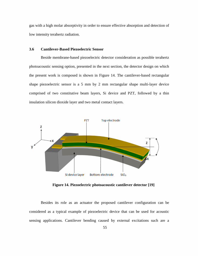
55
gas with a high molar absorptivity in order to ensure effective absorption and detection of
low intensity terahertz radiation.
3.6 Cantilever-Based Piezoelectric Sensor
Beside membrane-based piezoelectric detector consideration as possible terahertz
photoacoustic sensing option, presented in the next section, the detector design on which
the present work is composed is shown in Figure 14. The cantilever-based rectangular
shape piezoelectric sensor is a 5 mm by 2 mm rectangular shape multi-layer device
comprised of two constitutive beam layers, Si device and PZT, followed by a thin
insulation silicon dioxide layer and two metal contact layers.
Figure 14. Piezoelectric photoacoustic cantilever detector [19]
Besides its role as an actuator the proposed cantilever configuration can be
considered as a typical example of piezoelectric device that can be used for acoustic
sensing applications. Cantilever bending caused by external excitations such are a
56
uniformly distributed acoustic (pressure) loads p will result in non-uniform stress
distributions in cantilever constitutive layers. Tensile stresses are induced in the upper
cantilever plate (PZT) while compressive stresses are induced in the lower (Si device
layer) plate in the direction of the length of the beam. Consequently, due to this non-
uniformity in stress distribution with maximum values that occur at the top and bottom
PZT sides’ negative electrical charges are generated at the PZT top side while positive
charges at the bottom of PZT element.
Since at the top surface,
P₃ = d₃₁T₁, [15] (48)
where P₃ is polarization in the thickness direction in units of C/m², T₁ is stress in the
length direction in units of N/m², and d₃₁ is the transverse piezoelectric coefficient (C/N);
at the bottom surface,
P₃ = d₃₁ (-T₁), (49)
d₃₁ is a negative value for piezoelectric materials such as PbZr0.52Ti0.48O3. Therefore, due
to the direct piezoelectric effect an open circuit voltage is built up across PZT sensing
element. For sensing applications, high generated voltage is frequently desired. In respect
to that the effect of variations in models’ geometrical dimensions and impact of materials
electromechanical properties on sensing performance has been investigated. The initial

57
modeling and model performance investigations of presented configuration (Figure 16)
has been performed on device with the layer thickness of 5µm and the thickness of
remaining layers of 0.1 µm. As research progressed, based on this early work a number
of various geometry configurations have been designed and investigated using both;
analytical and FEM modeling methods. The device geometry has been constantly
changed and analyzed until configuration with the best sensing performance in terms of
maximum voltage sensitivity has been observed. Besides presented single beam
configuration another two beam-based sensing options have been designed and
investigated accordingly. One of mentioned configurations is solution involving four
single cantilever based sensors whose L-Edit design layout shown in Figure 15 below.
Figure 15. Four cantilevers sensing configuration
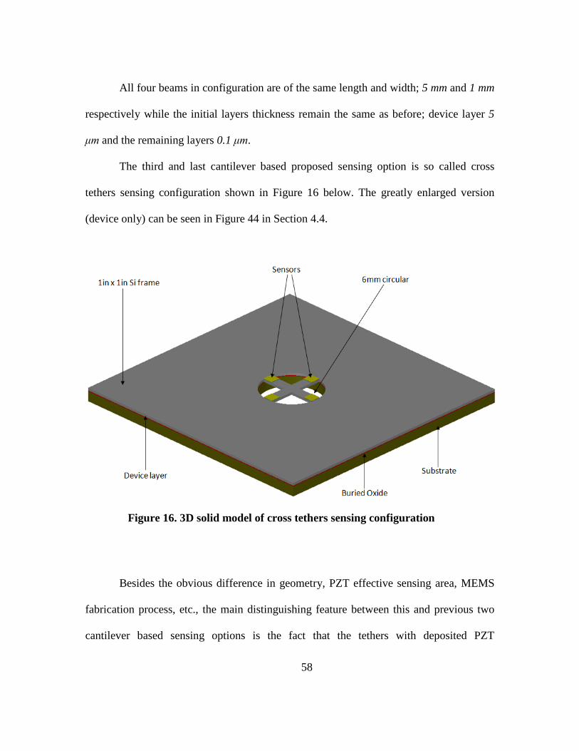
58
All four beams in configuration are of the same length and width; 5 mm and 1 mm
respectively while the initial layers thickness remain the same as before; device layer 5
μm and the remaining layers 0.1 μm.
The third and last cantilever based proposed sensing option is so called cross
tethers sensing configuration shown in Figure 16 below. The greatly enlarged version
(device only) can be seen in Figure 44 in Section 4.4.
Figure 16. 3D solid model of cross tethers sensing configuration
Besides the obvious difference in geometry, PZT effective sensing area, MEMS
fabrication process, etc., the main distinguishing feature between this and previous two
cantilever based sensing options is the fact that the tethers with deposited PZT

59
transducers on their top sides now acting as cantilever with both fixed ends. The expected
impact of this design change and many other design issues relating to this and the other
two configurations on the overall device sensing performance are analyzed and presented
in Chapter IV.
3.7 Membrane-Based Piezoelectric Sensor
This section serves to summarize modeling approach of the two, membrane-based
piezoelectric sensors’ configurations as simulated in CoventorWare®. In addition to
previously presented cantilever modeling the motivation of this work was to investigate
feasibility of different terahertz photoacoustic sensing options using different sensing
element geometry. In recent years acoustic devices such are a thin, flat multilayer silicon
membranes combined with a good quality of piezoelectric thin films have been developed
by MEMS technology resulting in a various novel micro-devices among which are
acoustic sensors, accelerometers, actuators or pressure sensors [21]. Based on some
research reports it has been found that the circular membranes fabrications often have
experienced some difficulties mainly due to its complex traditional bulk micromachining
fabrication process [22]. However, bulk micromachining through silicon substrates using
Deep Reactive Ion Etching (DRIE) is possible to achieve high aspect ratio deep etches.
Moreover, MEMS membrane is considered highly sensitive acoustic sensing device
which like piezoelectric cantilever under low pressure loadings produces an electrical
output (voltage). So, all these considerations and requirements for detecting very weak
terahertz photoacoustic radiation imply that the use of piezoelectric membrane as a sensor
sounds as reasonable design solution. One of the sensing options presented here is a thin
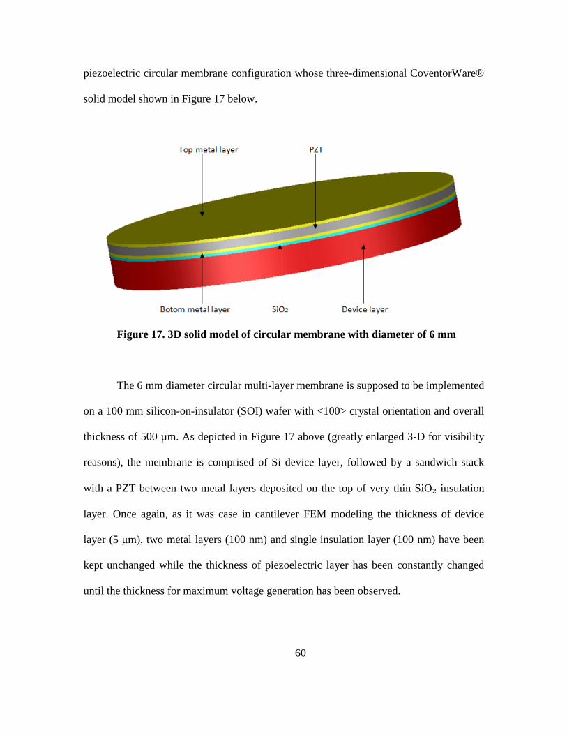
60
piezoelectric circular membrane configuration whose three-dimensional CoventorWare®
solid model shown in Figure 17 below.
Figure 17. 3D solid model of circular membrane with diameter of 6 mm
The 6 mm diameter circular multi-layer membrane is supposed to be implemented
on a 100 mm silicon-on-insulator (SOI) wafer with <100> crystal orientation and overall
thickness of 500 µm. As depicted in Figure 17 above (greatly enlarged 3-D for visibility
reasons), the membrane is comprised of Si device layer, followed by a sandwich stack
with a PZT between two metal layers deposited on the top of very thin SiO₂ insulation
layer. Once again, as it was case in cantilever FEM modeling the thickness of device
layer (5 μm), two metal layers (100 nm) and single insulation layer (100 nm) have been
kept unchanged while the thickness of piezoelectric layer has been constantly changed
until the thickness for maximum voltage generation has been observed.

61
The second membrane considered as potential sensing solution is the square
membrane configuration whose L-Edit design layout and 3-D FEM solid model shown in
Figure 18 and Figure 19 respectively.
Figure 18. L-Edit D square membrane design layout

62
Figure 19. CoventorWare 3D solid model of square membrane
The membrane has been implemented on the same silicon wafer, having the same
electromechanical properties as it was case in any of the previous sensing configurations
while the CoventorWare® fabrication process for each design option has been slightly
changed due to the different detectors’ geometry. As indicated in Figure 19 above, the
four piezoelectric transducers of the same size (300μm x 300μm) and shape have been
deposited on four symmetrically separated membranes’ locations. Besides the obvious
difference in the geometry the most significant and important characteristic which
distinguish this configuration from others is a very small PZT sensing area. After
importing the 2-D device design layouts from L-Edit©, the CoventorWare® 3-D solid
models generation, and conducted mesh analysis and adequate mesh generation both
configurations have been then simulated and analyzed using appropriate FEM domain
solver. The specific membranes’ multi-layer structures have been designed simulated and
tested mainly utilizing the mechanical and piezoelectric domain solvers. The Chapter IV

63
discuss, evaluate and compare the sensing performance of both proposed membrane-
based sensing configurations including the way in which analysis has been conducted.
3.8 Stochastic Cantilever Modeling
As mentioned in Section 2.8 statistics has an important role in the statistical
analysis of physical phenomena. In addition to Section 2.4 (Piezoelectric sensing) this
section presents stochastic response analysis of piezoelectric sensor such is piezoelectric
cantilever which has been used and analyzed as sensing element in a number of sensing
configurations presented in this research work. When an acoustic pressure load P is
applied to one side of a single piezoelectric element (beam) as shown in Figure 20, a
fraction of the applied pressure will be converted to an electric charge on the opposite
element’s side. For the purpose of this analysis the applied pressure P and amount of the
created electric charge (Voltage V) has been approximated by a Gaussian Probability
Density Function (PDF) and monotonic transfer function respectively.
Figure 20. Pressure loaded beam
The main purpose of this analysis was to investigate the conversion relationship
between pressure and electrical charge (voltage) which provides a deeper insight and

64
understanding in the area of electromagnetic terahertz radiation sensing. As depicted in
Figure 21 the two main regions where this conversion in fact occurs and on which this
analysis is based are;
Region 1: 0 < P < Pc → V = 0 and Region 2: Pc < P <∞ → V= αP where Pc is critical or
threshold pressure.
Figure 21. Voltage generation as function of applied pressure on top of PZT beam
The applied pressure P (acoustic load) on the top of piezoelectric beam
(transducer) is approximated by Gaussian PDF (Section 2.8, equation 28).
𝑃 = 𝑓𝑃(𝑃)1
√2𝜋 𝜎𝑝exp �−(𝑃−𝑃𝑚)2
2𝜎²𝑝�, where P is the pressure (random variable), and
Pm is mean.
The created amount of the charge (voltage V) on the bottom of piezoelectric beam
is assumed to be as

65
𝑉 = 𝛼𝑃 = 𝛼(𝑃 − 𝑃𝑐) (50)
Then the function that describes transformation of pressure P into electrical voltage V is
given by monotonic transfer function
𝑓𝑉(𝑣) = 𝑓𝑃(𝑃 = 𝑣𝛼
)| 𝑑𝑃𝑑𝑉
| [11] (51)
We need to know what is 𝑓𝑉(𝑣) and 𝑃(𝑉=0), where 𝑓𝑉(𝑣) is the voltage distribution
on the bottom sensors’ side and 𝑓𝑉(𝑣) is the probability mass function, i.e. probability
that 𝑉 = 0.
As 𝑓𝑉(𝑣) = 𝑓𝑃(𝑃 = 𝑣𝛼
)| 𝑑𝑃𝑑𝑉
|, and
𝑉 = 𝛼𝑃 = 𝛼(𝑃 − 𝑃𝑐 )
𝑉 = 𝛼𝑃 − 𝛼𝑃𝑐 → 𝛼𝑃 = 𝑉 + 𝛼𝑃𝑐 → 𝑃 = 𝑉𝛼
+ 𝑃𝑐, then
𝑓𝑉(𝑣) = 𝑓𝑃(𝑃 = 𝑣𝛼
+ 𝑃𝑐)| 𝑑𝑃𝑑𝑉
|, using Gaussian PDF and substitutes for
𝑃 = 𝑉𝛼
+ 𝑃𝑐, gives
𝑓𝑃(𝑝) = 1√2𝜋 𝜎𝑝
exp �−(𝑃−𝑃𝑚)2
2𝜎²𝑝� | 𝑑𝑃
𝑑𝑉|,
Once again substitute for 𝑑𝑝𝑑𝑉
= 1 𝛼
into above give us
𝑓𝑉(𝑣) = 𝑓𝑃(𝑃) = 1√2𝜋 𝜎𝑝
exp �−�𝑉
𝛼+𝑃𝑐−𝑃𝑚�2
2𝜎²𝑝� 1
𝛼

66
Rearranging exponential part in numerator for 𝛼 provide
𝑓𝑉(𝑣) = 1√2𝜋 𝜎𝑝
exp �−(𝑉+𝛼𝑃𝑐−𝛼𝑃𝑚)2
𝛼2
2𝜎²𝑝� 1
𝛼 , and further simplification gives
𝑓𝑉(𝑣) = 1𝛼 √2𝜋 𝜎𝑝
exp �−[𝑉−(𝛼𝑃𝑚−𝛼𝑃𝑐)]2
2𝜎²𝑝𝛼2 �
Thus, for V < 0 → 𝑓𝑉(𝑣) = 0,
while for V ≥ 0 → 𝑓𝑉(𝑣) = 1𝛼 √2𝜋 𝜎𝑝
exp �−[𝑉−(𝛼𝑃𝑚−𝛼𝑃𝑐)]2
2𝜎²𝑝𝛼2 �
Then we can say that voltage distribution on the bottom beams’ side is also random
variable with Gaussian PDF, i.e.
V ≈ N (𝛼𝑃𝑚 − 𝛼𝑃𝑐, 𝜎𝑃2 𝛼2),
where N is the Normal or Gaussian distribution.
Furthermore, probability that V = 0 i.e. P (V = 0) (Figure 22)

67
Figure 22. PDF for V=0 for Pc > α (Pm – Pc)
By definition 𝛼 > 0 and 𝜎𝑝 > 0 ,
𝑃(𝑉=0) = 𝑃(−∞ < 𝑃 < 𝑃𝑐)
𝑃(𝑉=0) = ∫ 1√2𝜋 𝜎𝑝
𝑃𝑐−∞ 𝑒− (𝑃−𝑃𝑚)2
2𝜎²𝑝 𝑑𝑝 for 𝑃𝑐 > 𝛼𝑃𝑚 − 𝛼𝑃𝑐
Considering integral ∫ 1𝜎√2𝜋
𝑒−�(𝑥−𝜇)2
2𝜎2 �𝑥0 𝑑𝑥 = − 1
2�erfc �−𝑥+𝜇
𝜎√2��,
where erfc is error function; erfc(x) = ∫ 𝑒−𝑡2𝑑𝑡 = 1 − erfc(x)𝑥0 , then
𝑃(𝑉=0) = ∫ 1√2𝜋 𝜎𝑝
𝑒−(𝑃−𝑃𝑚)2
2𝜎²𝑝𝑃𝑐−∞ 𝑑𝑃
𝑃(𝑉=0) = − 12
�𝑒𝑟𝑓𝑐(∞) − �− 12
erf �−𝑃𝑐+𝑃𝑚𝜎𝑃√2
���, as 𝑒𝑟𝑓𝑐(∞) = 1 then
𝑃(𝑉=0) = − 12
+ 12
erf �−𝑃𝑐+𝑃𝑚𝜎𝑃√2
� , for 𝑃𝑐 < 𝛼𝑃𝑚 − 𝛼𝑃𝑐
𝑥

68
So, as depicted in Figure 23 for result we have negative distribution.
Figure 23. PDF for V=0 for Pc > α (Pm – Pc)
Based on the presented statistical analysis, all what has been said so far in relation
to the voltage distribution (charge distribution) on the bottom side of PZT element can be
summarized through the following two cases;
a. If variance 𝜎𝑃2 = 1 and mean 𝑃𝑚 = 0, and substituting it into obtained
voltage PDF 𝑓𝑉(𝑣) = 1𝛼 √2𝜋 𝜎𝑝
exp �−[𝑉−(𝛼𝑃𝑚−𝛼𝑃𝑐)]2
2𝜎²𝑝𝛼2 �, the expected distribution
is as shown in Figure 24.

69
Figure 24. Voltage PDF for Variance =1, and mean Pm = 0
b. If 𝑃𝑚 = 1 and 𝜎𝑃2 = 0 then, as shown in Figure 25 there is no voltage
generation on the bottom of piezoelectric beam.

70
Figure 25. Voltage PDF for Variance = 0, and mean Pm = 1
Furthermore, pressure is always 𝑃𝑚, and its distribution can be approximated by
Dirac function (Figure 26).
Figure 26. Approximated (Dirac) pressure PDF
71
Then, as P {P = Pm} = 1 and P {P ≠ Pm} = 0 the voltage value is always given
as P {𝑉 = 𝛼(𝑃𝑚 − 𝑃𝑐)} = 1.
In summary, from a statistics point of view this analysis has shown that uniformly
distributed pressure P on the top of piezoelectric beam as a random variable (Gaussian
PDF) will result also in random Normal Gaussian voltage distribution variable
parameters 𝜎𝑝 and 𝑃𝑚 on the bottom of PZT beam.
3.9 Summary
The main focus of this chapter was on the modeling process of the proposed
terahertz photoacoustic detector configurations as potential sensing solutions,
firstly with an accent on a theoretical modeling of the sensing effects of
cantilever-based piezoelectric sensors. Next, the sensors’ FEM simulations
modeling approach was covered through the full description of each FEM
modeling stage based on the use of CoventorWare® simulation tools. Moreover,
the importance and the role of the photoacoustic spectroscopy in the terahertz
photoacoustic detection process have been outlined. Due to the high degree of gas
involvement in the photoacoustic sensing process, the kinetic theory of gasses was
used in order to develop firm understanding of the required sample gas pressure
change calculations inside the photoacoustic cell. To complete the whole
modeling process it was important to select the sensors that will be employed. The
ones selected are the cantilever and membrane based piezoelectric sensors. In the

72
last chapter section a theoretical approach of stochastic cantilever modeling is
presented.
IV. Results and Analysis
4.1 Chapter Overview
This chapter discusses and analyzes five different MEMS sensor configurations
that could be considered as potential sensing solutions for the intended THz photoacustic
detector design. The chapter provides analytical as well as FEM analysis for the three
different cantilever-based single piezoelectric layer rectangular shape sensor
configurations. In addition two sensing options involving multi-layer circular and square
membranes are introduced.
4.2 Rectangular piezoelectric cantilever beam – Configuration I
This section reflects on the analytical and FEM modeling of the single
piezoelectric layer rectangular shape cantilever, whose L-Edit cross section is shown in
Figure 27, and it presents results analysis and discussion of sensing Configuration I.

73
Figure 27. Cantilever L-Edit cross-section
As already mentioned in Section 2.11 the initial fabrication of the proposed
cantilever is performed on a 100 mm Silicon On Insulator (SOI) wafer with <100>
crystal orientation and overall thickness of 500µm. The thickness of the device layer is
5μm while the cantilever length and width are 5 mm and 2 mm respectively. Since the
cantilever will act as a piezoelectric photoacoustic transducer there is a requirement for
deposition of a thin PZT film on top of the 5 μm device layer. The additional layers as
shown in the figure above are deposited on top of each other, starting with SiO₂ as an
insulation layer followed by a sandwich stack with a PZT between two metal (platinum)
layers. The proposed beam geometry with optimal device and PZT layer thickness ratio B
for maximum voltage sensitivity is intended to be used in the following sensor
configuration (Figure 28).

74
Figure 28. CoventorWare 3D solid model cantilever configuration
In addition, the configurations with device layer thickness of 10μm and 20μm are
considered and analyzed as possible solution options. The expected functional
performance of the sensor in development mainly depends on the cantilever geometrical
dimensions and the elastic and electromechanical properties of the two beams’
constitutive layers, namely device (mechanical) and PZT layer. The thickness of the
remaining layers in this configuration is kept very small in order to minimize their effects
on detectors’ sensing performance. The cantilever electromechanical properties can be
more or less summarized by defining the Young’s modulus and the dielectric constants of
the piezoelectric and device layers, the transverse piezoelectric coefficient and transverse
piezoelectric coupling coefficient. In recent years PZT has been an attractive choice for

75
MEMS application mainly due to its high piezoelectric coefficient. Among others are
zinc-oxide (ZnO), Aluminum Nitride (AlN), polyimide or Polyvinylidene Fluoride
(PVDF), but their use has been restricted in MEMS to certain extent, mainly due to very
low piezoelectric coefficients [23]. Therefore, based on research work and published
results in the past years, Silicon (Si) and PZT are known as materials with the best
electromechanical coupling properties, and as such have been selected as preferred option
for the sensor in development. The selection of silicon as a cantilever mechanical layer
has been based on the requirement for a stiffer mechanical layer with clamping properties
capable to ensure desired PZT dielectric constant decrease.
Based on analytical and FEM modeling methods presented in Chapter III and on
all these considerations from above the rest of this section presents cantilever
performance analysis using both analytical and finite element approach. In both cases a
comprehensive investigation for a variety of beams configurations has been conducted. In
this case the different beams’ configurations refer to different thickness ratio 𝐵 = 𝑡𝑚𝑡𝑝
between the device and PZT layers, while the cantilever length L=5 mm and width w=2
mm remain the same. The thickness ratio 𝐵 for cantilever maximum voltage sensitivity
can be achieved in two different ways; keeping the piezoelectric layer thickness 𝑡𝑝 fixed,
while the elastic layer is etched by appropriate etching solution (wet or dry etching) to
desired thickness 𝑡𝑚, or a more common approach (assumed in this sensor modeling) is
to keep the elastic layer thickness 𝑡𝑚 fixed, while the piezoelectric layer of desired
thickness 𝑡𝑝 is deposited onto the elastic layer.
76
Using either of these two approaches it is obvious that the optimal thickness ratio
B must be somewhere between two limiting cases; between B→0 and B→∞. When B→0
the cantilever becomes almost pure monolithic piezoelectric structure as the thickness 𝑡𝑚
becomes negligibly small in comparison with 𝑡𝑝. Applying external load p to this
monolithic piezoelectric beam will not produce the expected voltage generation. Simply,
the cantilever will not act as transducer at all. Applied terahertz photoacoustic signal will
cause cantilever bending; however, due to polarization of the piezoelectric beam in the
beam’s thickness direction, the same electric charge will be generated on the top and the
bottom PZT surface. As voltage, by definition is a difference between potentials (open
circuit voltage) in this case the difference is zero and the overall voltage across PZT plate
is zero. In case B→∞ the cantilever becomes very monolithic Si structure. Applying
pressure on the top of this beam configuration will not cause electric charge generation
(no piezoelectric material involved in structure) and electric voltage will once again
approach zero. Therefore, as mentioned above a maximum generated voltage is expected
to be observed somewhere between the boundary conditions.
4.2.1 Theoretical Analysis
Based on the analytical modeling presented in Section 2.7 and Section 3.2 and the
derived model equations for generated cantilever capacitance C (equation 23), electrical
charge Q (equation24) and open circuit electric voltage V (equations 25 and 26),
comprehensive cantilever analysis for a wide range of thickness ratios B has been
conducted in order to determine the best beam configuration in terms of maximum
voltage sensitivity. The sensor in development is supposed to detect relatively weak
(1mW - 3mW) THz radiation signals, which after their conversion into photoacoustic

77
radiation are expected to produce very small pressure loads on the top of PZT plate. As
presented in Section 3.4 the expected THz photoacoustic pressure loads fall within μPa
and mPa pressure range. Which photoacoustic range will be employed mainly depends
on the absorption properties (ε) of the gas surrounding the cantilever inside the
photoacoustic cell, the power of the terahertz source and terahertz radiation modulation
frequency. Taking into account the expected sensitivity level the cantilever behavior
investigations have been conducted for the entire μPa and mPa pressure range. The
configurations which have not responded significantly (to measurable level) to the loads
within prescribed pressure range are not considered as possible sensing solution and have
not been subject for the further investigations. During the analysis, device layer
thickness 𝑡𝑚 has been kept fixed while the thickness of the PZT layer 𝑡𝑝 has been
continuously changed in appropriate thickness increments until the thickness ratio B for
maximum voltage sensitivity has been observed. In respect to that the cantilever
configurations with variable 𝑡𝑝 and fixed device layer thickness of 𝑡𝑚 = 5μm, 𝑡𝑚=
10μm, and 𝑡𝑚= 20μm with 𝑡𝑝 ranging from 0.1μm up to 𝑡𝑝=3.3μm with an increment
rate of 0.1μm have been continuously investigated for a pressure range defined in Section
3.4 (1 μPa up to 1 Pa).
Cantilever response to a range of uniformly distributed pressure loads p has been
observed in respect to each single beam configuration as well as in a case of gradual PZT
layer thickness increments. As expected, in a case of single beam configuration, i.e.
configuration with a unique 𝑡𝑚 and 𝑡𝑝 an increase in applied pressure load p will cause
more beams’ bending, more electric charge; Q is going to be generated and a linear

78
increase in the open circuit voltage V across PZT will be observed while the capacitance
C for analyzed 𝑡𝑚 and 𝑡𝑝 combination remains constant regardless of the pressure
increments. An illustration of the mentioned observation for a beam with L= 5mm, w=2
mm, 𝑡𝑚=5 μm and 𝑡𝑝=100 nm for entire mPa pressure range (1mPa to 1Pa) can be seen
in Figure 29 and Figure 30, respectively.
Figure 29. Cantilever PZT charge distribution
0 0.1 0.2 0.3 0.4 0.5 0.6 0.7 0.8 0.9 1-3.5
-3
-2.5
-2
-1.5
-1
-0.5
0x 10
-9 Charge Distribution
Pressure in [Pa]
Cre
ated
Cha
rge
[pC
]

79
Figure 30. Open circuit voltage V across PZT
In addition to presented MATLAB plots the same observations related to the same
beam length L, width w, and thickness 𝑡𝑚 and 𝑡𝑝 of 0.1 μm, 0.5 μm, and 1 μm for a
pressure range portions of 0.1 mPa, 0.5 mPa, 1 mPa, 0.5 Pa and 1 Pa can be seen in the
following tables: Table 2, Table 3 and Table 4.
Table 2. Voltage distribution for tp=100 nm
p 0.1 mPa 0.5 mPa 1 mPa 0.5 Pa 1 Pa
V [V] -1.39e-7 -6.98e-7 -1.39e-6 -0.69e-3 -1.39e-3
C [pF] 2.31e-6 2.31e-6 2.31e-6 2.31e-6 2.31e-6
0 0.1 0.2 0.3 0.4 0.5 0.6 0.7 0.8 0.9 1-1.4
-1.2
-1
-0.8
-0.6
-0.4
-0.2
0x 10
-3 Open Circuit Voltage
Pressure in [Pa]
Vol
tage
[V]

80
Table 3. Voltage distribution for tp = 500nm
P 0.1 mPa 0.5 mPa 1 mPa 0.5 Pa 1 Pa
V [V] -5.94e-7 -2.97e-6 -5.94e-6 -2.97e-3 -5.94e-3
C [pF] 4.74e-7 4.74e-7 4.74e-7 4.74e-7 4.74e-7
Table 4. Voltage distribution for tp=1μm
P 0.1 mPa 0.5 mPa 1 mPa 0.5 Pa 1 Pa
V [V] -9.74e-7 -4.87e-6 -9.74e-6 -4.87e-3 -9.74e-3
C [pF] 2.42e-7 2.42e-7 2.42e-7 2.42e-7 2.42e-7
Furthermore, keeping the device layer 𝑡𝑚 = 5 𝜇𝑚 fixed and increasing 𝑡𝑝 in
mentioned increments steps, it has been observed that in a case of any 𝑡𝑝 increment in
comparison with previous beam thickness ratio B even there is less beams’ bending (due
to the overall beam thickness increase) and less electric charge Q generation for the same
pressure loads; the open circuit voltage V across PZT element still increases linearly. This
is true and is going to happen for any 𝑡𝑝 increment until thickness ratio B for maximum
voltage sensitivity has been once reached. The reason for this gradual voltage increase is
mainly due to the change in configuration capacitance C. It is true that when
increasing 𝑡𝑝 and consequently increasing the overall cantilever thickness there is less
beam bending under the same pressure loads and the amount of generated electric charge

81
Q slightly decreases, and in accordance with the direct piezoelectric effect we should
expect an open circuit voltage V decrease, too. However, due to the fact that the
generated voltage V = 𝑄 𝐶
and that the total configuration capacitance C decreases much
more rapidly than the decrease in the generation of the electric charge Q is; then the
actual voltage V in fact increases. Therefore, based on the obtained calculation results, the
thickness ratio for the maximum voltage sensitivity occurred to be B=1.96 and it belongs
to the cantilever configuration with the device layer thickness of 𝑡𝑚 = 5 𝜇𝑚 and 𝑡𝑝 =
2.55 𝜇𝑚. The following table (Table 5) shows the generated electrical voltages V across
the PZT layers for indicated 𝑡𝑝 increments and applied pressure load p of 1Pa.
Table 5. Generated voltage across PZT layers for p=1Pa
PZT thickness 𝑡𝑝 [μm] Voltage V [mV] 2 -13.316
2.1 -13.481 2.2 -13.622 2.3 -13.719 2.4 -13.749 2.5 -13.765 2.55 -13.767 2.6 -13.766 2.9 -13.699 2.7 -13.754 2.8 -13.732 3 -13.657
It can be seen that the maximum open circuit voltage V of - 13.767 mV has
been generated across piezoelectric layer with corresponding thickness of 𝑡𝑝 = 2.55 μm.
So, the thickness ratio of B=1.96 is a configuration turning point at which the cantilever

82
as a photoacoustic sensor for any pressure load p will most likely be able to detect THz
photoacoustic radiation. Any increase or decrease in B, i.e. any deviation from 1.96 will
decrease the overall configuration sensitivity. It basically means (as highlighted in Table
5) that for a cantilever with fixed device layer thickness to 5μm any increase in 𝑡𝑝 above
2.55 μm or any decrease in 𝑡𝑝 below 2.55 μm will for result have a decrease in the
amount of generated voltage V across PZT layer. These observations are depicted in the
following MATLAB plot (Figure 31) which represents voltage generation across PZT
layer as function of thickness ratio B. It can be clearly seen that analyzed sensing
configuration for any photoacoustic load within predicted pressure range exhibits highest
sensitivity (maximum voltage generation) for B= 1.96.
Figure 31. Calculated cantilever voltage generation as function of thickness ratio B
0 2 4 6 8 10 12 14 16 180
0.002
0.004
0.006
0.008
0.01
0.012
0.014Calculated B for Maximum V Sensitivity, te=5microm
Thickness Ratio B
Vol
tage
V [
V ]
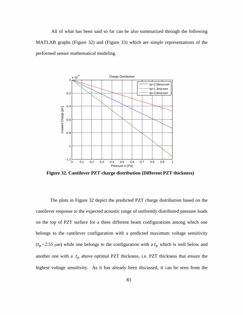
83
All of what has been said so far can be also summarized through the following
MATLAB graphs (Figure 32) and (Figure 33) which are simple representations of the
performed sensor mathematical modeling.
Figure 32. Cantilever PZT charge distribution (Different PZT thickness)
The plots in Figure 32 depict the predicted PZT charge distribution based on the
cantilever response to the expected acoustic range of uniformly distributed pressure loads
on the top of PZT surface for a three different beam configurations among which one
belongs to the cantilever configuration with a predicted maximum voltage sensitivity
(𝑡𝑝=2.55 μm) while one belongs to the configuration with a 𝑡𝑝 which is well below and
another one with a 𝑡𝑝 above optimal PZT thickness, i.e. PZT thickness that ensure the
highest voltage sensitivity. As it has already been discussed, it can be seen from the
0 0.1 0.2 0.3 0.4 0.5 0.6 0.7 0.8 0.9 1-1.2
-1
-0.8
-0.6
-0.4
-0.2
0x 10
-9 Charge Distribution
Pressure in [Pa]
Cre
ated
Cha
rge
[pC
]
tp=2.55micromtp=1.3micromtp=3.9microm

84
displayed plots that in a case of variable piezoelectric layer configurations it is not always
true that a configuration with the largest amount of generated charge Q will in fact
produce voltage with highest magnitude across PZT element. From Figure 32 it can be
seen that the highest amount of generated charge Q belongs to the configuration with 𝑡𝑝
of 1.3 μm (well below optimal PZT thickness) while from Figure 33 it can be seen that
the maximum voltage generation actually belongs to the configuration with 𝑡𝑝of 2.55 μm.
Figure 33. Open circuit voltage V across PZT (Different PZT thickness)
Moreover, in relation to Figure 33 it was intended to plot on the same graph the
voltage distributions across cantilever PZT layers for 𝑡𝑝 of 2.55 μm, 2.5 μm and 2.6 μm
(i.e. configurations with close PZT thickness) in order to match the Table 5 calculation
0 0.1 0.2 0.3 0.4 0.5 0.6 0.7 0.8 0.9 1-0.014
-0.012
-0.01
-0.008
-0.006
-0.004
-0.002
0Open Circuit Voltage
Pressure in [Pa]
Vol
tage
[V]
tp=2.55micromtp=1.3micromtp=3.9microm
85
results as close as possible and observe actual turning points in the open circuit voltage
increase/decrease, but due to the extremely small difference between the so called turning
points voltages, the actual plotting would produce graphs overlapping which could not be
used for effective visual model analysis. However, the selections of any 𝑡𝑝 below and
above 2.55 μm that will ensure minimum required plotting visibility do not have any
impact on the analysis validity.
Furthermore, the configurations with the device layer thickness of 10 μm and
20μm are considered and analyzed as possible solution options. The mentioned
configurations have been investigated in the same way and under the same analytical
assumptions as 5 μm device layer configuration. The brief results summary related to the
configurations’ voltage sensitivity levels and their comparisons among each other for the
randomly selected 𝑡𝑚 and 𝑡𝑝 combinations and pressure load of 1Pa is presented in
Table 6.

86
Table 6. Voltage distribution across PZT for p=1 Pa and various tm, tp configuration combinations
Elastic layer 𝑡𝑚 [μm]
PZT layer 𝑡𝑝 [μm]
V [mV]
5 0.1 -1.39 10 0.1 -0.37 20 0.1 -0.10 5 0.2 -3.35 10 0.2 -0.74 20 0.2 -0.19 5 0.3 -3.86 10 0.3 -1.08 20 0.3 -0.29 5 0.4 -4.95 10 0.4 -1.41 20 0.4 -0.38 5 0.5 -5.94 10 0.5 -1.73 20 0.5 -0.47 5 1 -9.74 10 1 -3.13 20 1 -0.89
The presented results show that any increase in the elastic layer thickness 𝑡𝑚 will
cause decrease in the cantilever voltage sensitivity. It is true that voltage sensitivity for
configurations with elastic layer thicknesses of 10 μm and 20 μm can be improved by
finding appropriate thickness ratio B (increasing 𝑡𝑝) but it requires further piezoelectric
layer thickness increase that will have for a result an undesirable (already thick) overall
beam thickness increase. Thus, the sensor becomes too thick and too difficult to bend. As
THz photoacoustic pressure loads are expected to be within μPa or mPa pressure range, it
is obvious that bending will not occur and configurations like these cannot be considered
as potential solutions.

87
4.2.2 FEM Analysis
The CoventorWare® FEM simulations were performed on the same cantilever
configurations used in the analytical modeling in order to investigate the effect of
variations in the thickness on the microcantilever voltage sensitivity. The simulations
have been conducted, analyzed and compared with the theoretical computations
presented in the previous sub-section (4.2.1). As pointed out in the FEM Modeling
section (Section 3.3) the CoventorWare® simulation software is known as the most
comprehensive suite of MEMS design tools and as such has been used extensively in
these project investigations. Due to the nature and the purpose of this research assignment
and the specific cantilever multi-layer structure, advanced CoventorWare® simulations
and testing, utilizing mechanical (MemMech) and the piezoelectric domain solver
(MEMPZE) have been conducted. MemMech is used to compute the mechanical
solutions for the cantilever, mainly to solve for mechanical stress and displacement as
well as modal analysis calculations in order to compute the natural resonant frequencies
of the sensor structure, while MEMPZE is used to investigate the cantilever piezoelectric
behavior in terms of electrical charge (voltage) generation.
In accordance with the FEM simulation modeling process presented in Chapter
III, based on the actual 2-D L-Edit© device layout designs, the cantilever 3-D solid
models for configurations with L=5 mm, w=2 mm and device layers thicknesses of 5 μm,
10 μm and 20 μm have been generated first. In each generated solid model configuration,
as it was case during the analytical cantilever modeling the thickness of the top and the
bottom metal layers including SiO2 layers were 0.1 μm, while the thickness of the PZT
layers was varied from 0.1 μm to 3.3 μm with increments of 100 nm.

88
An accurate model is essential to the function of a sensor; thus, before progressing
further with a full model simulation and the testing process, utilizing the
CoventorWare® domain solvers, the adequate mesh analysis and model meshing have
been conducted in order to obtain acceptable results accuracy in an acceptable amount of
computation time. In this cantilever modeling, due to its orthogonal geometry the
Manhattan bricks mesh model has been chosen as the most appropriate meshing option.
For this particular beam structure with cantilever length L=5 mm, width w=2 mm and the
overall beam thickness of 8 μm (the device and PZT layer thickness is 5 μm and 2.7 μm
respectively, plus two metal and one oxide layer each of individual thickness of 0.1 μm)
the same analysis has been run for the models with mesh densities shown in Table 7.
Table 7. Cantilever response to uniformly distributed pressure load of 1Pa
Mesh model number
Mesh size in x,y, z direction [μm] Deflection [μm]
1 1000x1000x1000 14.60506 2 500x500x500 14.60506 3 300x300x300 14.27953 4 200x200x200 14.20623 5 100x100x100 14.20623
From the obtained results, presented in Table 7, it can be seen that the analyzed
cantilever configuration deflection response converges to a unique numerical value as the
mesh density increase. As the two meshes (minimum requirement), mesh model number
4 and mesh model number 5 give essentially the same deflection results, the model can be
considered mathematically accurate. It is true that the mesh density could be increased

89
further but it will lead to negligible differences in results, but significant increase in
simulation time. Even the difference between mesh model number 3 and mesh model
number 5 is only 0.51%, and any further mesh refining will not have significant impact
on simulation accuracy. Once the model has been appropriately meshed reducing
cantilever geometry into smaller and simpler finite element bricks, the full FEM analysis
using CoventorWare® domain solvers has been conducted with confidence that the
model is producing mathematically accurate results. An illustration of meshed cantilever
configuration with optimal Manhattan bricks mesh density (x = 200 μm, y = 200 μm and
z = 200 μm) that has been used throughout sensor FEM analysis is shown in Figure 34.
Figure 34. Meshed cantilever model for tm =5 μm, tp=2.7 μm metal and SiO2 of 0.1 μm
The beam is 5 mm by 2 mm, so 250 bricks will be created for the beam layer in
the XY plane. The beam is only 8 μm in height, so the mesher will create a single layer of
bricks.

90
Once again as in the case of theoretical modeling the FEM simulation analysis has
been performed for a wide range of configurations, where the device layer thickness 𝑡𝑚
has been kept fixed while the thickness of the PZT layer 𝑡𝑝 has been continuously
changed in appropriate thickness increments until the thickness ratio B for maximum
voltage sensitivity has been observed. Specifically, the cantilever configurations with
variable 𝑡𝑝 and fixed device layer thickness of 𝑡𝑚 = 5 μm, 𝑡𝑚= 10 μm, and 𝑡𝑚= 20 μm
with 𝑡𝑝 ranging from 0.1 μm up to 𝑡𝑝=3.3 μm with an increment rate of 100 nm have
been simulated and analyzed for a pressure loads ranging from 1 μPa up to 1 Pa covering
entire μPa and mPa photoacoustic pressure range. As expected and already observed
during the theoretical modeling there is no exception here; different configurations have
responded differently, exhibiting different sensitivity levels under the same pressure
exposure. Before presenting and discussing the numerical collection of the obtained
results, an example of simulated cantilever configuration just as a visual illustration of
CoventorWare® FEM modeling can be seen in Figure 35. The resulting profile belongs
to the cantilever configuration with device and PZT layer thickness of 5 μm and 2.7 μm
respectively and optimal mesh density with Manhattan bricks element size of 200 μm x
200 μm x 200 μm. The individual thickness of metal and oxide layers is 0.1 μm. It can be
seen that the FEM simulation, in contrast to the analytical cantilever modeling, produces
a very smooth bended profile under the same uniformly distributed photoacoustic
pressure loads. The different resulting profiles produce different numerical descriptions
of cantilever piezoelectric sensing behavior in terms of electrical charge (voltage)

91
generation. The reasons and justification for these deviations between the two modeling
methods are presented and discussed later within the results comparison section.
Figure 35. Typical cantilever FEM simulation results
The CoventorWare® FEM simulations (Figure 35) were performed on a vast
number of beam configurations to investigate the effect of variations in thickness on the
cantilever voltage sensitivity. In order to determine the level of voltage response, in
addition to the geometry models the FEM analysis takes into account the cantilever
electromechanical properties, too. Hence, the FEM simulated voltage across cantilevers’
PZT layers is not just function of pure model geometry and mechanical properties of
materials involved in the structure; it is also a function of cantilever electrical (mainly
piezoelectric) and coupling properties. Furthermore, beside the numerical results, the
CoventorWare® FEM modeling offers a deeper meaningful insight into the device
behavior through its simulations, during the actual sensing process. It enables
visualization (see Figure 35 and Figure 36) of the expected amount of beam bending, the

92
stress distributions in cantilever thickness and length direction or expected charge
distributions across the cantilever surface.
Figure 36. Mises stress distribution of piezoelectric cantilever
4.2.2.1 Observations
The same investigation approach, previously used in theoretical cantilever
modeling, has been implemented, here but this time utilizing CoventorWare® FEM
modeling tools. Once again cantilever response to a wide range of uniformly distributed
pressure loads p has been investigated in both cases; single beam configurations and
configurations involving gradual PZT layer thickness increments. As pointed out
previously, the single beam configuration assumes observations related only to the beam

93
with unique elastic and piezoelectric layer thickness, i.e. observing the change in
cantilever response due to the change in applied acoustic load p only, but for the same
thickness ratio B. As expected, based on the performed observations and the obtained
simulation results, the way the cantilever responds is found to be the same as in the case
of mathematical modeling. In case of single beam configurations, any increase or
decrease in applied pressure load p will cause linear increase or decrease in open circuit
voltage generation. An illustration of the mentioned observation for investigated beam
configuration with L=5 mm, w=2 mm, 𝑡𝑚=5 μm and 𝑡𝑝 of 100 nm and 1 μm and pressure
load range of 1 mPa to 1 Pa can be seen in Figures 37 and Figure 38.
Figure 37. FEM voltage across 100 nm PZT layer
0 0.1 0.2 0.3 0.4 0.5 0.6 0.7 0.8 0.9 1-5
-4
-3
-2
-1
0
1x 10
-4 FEM Open Circuit Voltage for tm=5microm and tp=100nm
Pressure in [Pa]
Vol
tage
[V]

94
Figure 38. FEM voltage across 1μm PZT layer
In addition to the above plots the same observations for randomly selected
pressure loads p and piezoelectric layer thickness 𝑡𝑝 are presented in Table 8, Table 9 and
Table 10 respectively.
Table 8. CW FEM voltage distribution for tp = 100nm
p 0.1 mPa 0.5 mPa 1 mPa 0.5 Pa 1 Pa
V [V] -4.87e-8 -2.43-7e -4.87e-7 -2.49e-4 -4.87e-4
0 0.1 0.2 0.3 0.4 0.5 0.6 0.7 0.8 0.9 1-3.5
-3
-2.5
-2
-1.5
-1
-0.5
0x 10
-3 FEM Open Circuit Voltage for tm=5microm and tp=1microm
Pressure in [Pa]
Vol
tage
[V]

95
Table 9. CW FEM distribution for tp =1μm
p 0.1 mPa 0.5 mPa 1 mPa 0.5 Pa 1 Pa
V [V] -3.08e-7 -1.54e-6 -3.08e-6 -1.55e-3 -3.09e-3
Table 10. CW FEM distribution for tp =2.5μm
p 0.1 mPa 0.5 mPa 1 mPa 0.5 Pa 1 Pa
V [V] -4.09e-7 -2.05e-6 -4.09e-6 -2.05e-3 -4.09e-3
Furthermore, in order to determine the cantilever configuration with thickness
ratio B for a maximum voltage sensitivity, FEM modeling using the piezoelectric domain
solver, and MEMPZE have been conducted and analyzed for the wide range of beam
configurations, where the device layer thickness 𝑡𝑚 has been kept fixed (5μm), while the
PZT layer thickness 𝑡𝑝 has been continuously changed in appropriate thickness
increments until the thickness ratio B for a maximum voltage sensitivity has been
observed. In the same fashion as in the case of theoretical sensor modeling, the cantilever
configurations with variable 𝑡𝑝 and fixed device layer thickness to 𝑡𝑚 = 5 μm, 𝑡𝑚= 10
μm, and 𝑡𝑚= 20 μm with 𝑡𝑝 ranging from 0.1 μm up to 𝑡𝑝=3.3 μm and an increment rate
of 100nm have been continuously simulated and investigated for pressure loads ranging
from 1 μPa up to 1 Pa. The brief results summary for selected portion of simulated
results with highlighted open circuit voltage V that has been observed across piezoelectric

96
layer that belongs to configuration with maximum voltage sensitivity is shown in Table
11.
Table 11. CW FEM voltage across PZT layers for p=1Pa
PZT thickness 𝑡𝑝 [μm] Voltage V [mV] 0.1 -0.48733 1 -3.08735
2.5 -4.09210 2.65 -4.09832 2.7 -4.09836 2.8 -4.09569 2.9 -4.08995 3 -4.09836
On the strength of the FEM simulation results, the thickness ratio for the
maximum voltage sensitivity occurred to be B=1.85, and it belongs to the cantilever
configuration with the device layer thickness of 𝑡𝑚 = 5 𝜇𝑚 and 𝑡𝑝 = 2.7 𝜇𝑚. Once
again, as depicted in the MATLAB plot in Figure 39, it has been observed that any
change in thickness ratio B that deviates from 1.85 will cause the change (decrease) in
detector sensitivity.

97
Figure 39. FEM cantilever voltage generation as function of thickness ratio B
The more detailed analysis related to the cantilever behavior under uniform
distribution of pressure loads on the beam’s top surface is already discussed in the
theoretical analysis section (Section 4.2.1), and as such is fully applicable here. Due to
the same reasons, the analysis related to the configurations involving beams with device
layers of 10 μm and 20 μm and wide range of variable piezoelectric layers thickness are
intentionally omitted; however, will be discussed and analyzed within the results
comparisons section.
Finally, modal frequencies and shapes of a cantilever finite element model have
been calculated and visualized using CoventorWare® MemMech solver and 3D viewer.
The resonant frequencies and their associated mode shapes are of particular interest in
designing this, as well as the other sensor configurations presented in this research work
0 2 4 6 8 10 12 14 16 180
0.5
1
1.5
2
2.5
3
3.5
4
4.5x 10
-3 FEM B for Maximum V Sensitivity, te=5microm
Thickness Ratio B
Vol
tage
V [
V ]

98
because they indicate when the sensor will have its maximum response under uniformly
distributed photoacoustic pressure loads. The initial cantilever modal analysis has been
performed for the 100 Hz to 1600 Hz harmonic frequency range on the 10 mPa pressure-
loaded beam configuration with requested 10 frequencies display. The device is
examined for various mode shapes and its resonant frequencies are determined. The
resulting vibrating pattern of the investigated cantilever configuration for various modes
and the calculated natural resonant frequencies when the pressure load of 10 mPa is
applied on its top side is shown in Figure 40.

99
Mode 1 (508.223 Hz) Mode 2 (2533.68 Hz)
Mode 3 (3202.92 Hz) Mode 4 (8114.89 Hz)
Mode 5 (9043.71 Hz) Mode 6 (15183.9 Hz) Figure 40. Resulting vibrating pattern and resonant frequencies for a load of 10 mPa

100
Besides analyzing mode shapes (the deformation of the mechanical structure), the
understanding of the impact and the contribution of the individual mode shapes to the
harmonic cantilever response can be acquired by looking at the generated generalized
harmonic response results shown in Table 12 below.
Table 12. MemMech generalized harmonic display table
Frequency
[Hz] Mode 1 Mode 2 Mode 3 Mode 4 Mode 5 Mode 6
0 100 0.0331 7.574e-8 4.480e-4 1.810e-10 3.358e-5 6.220e-11
1 116.4 0.0336 7.578e-8 4.482e-4 1.810e-10 3.358e-5 6.220e-11
2 136.3 0.0343 7.584e-8 4.484e-4 1.810e-10 3.358e-5 6.220e-11
3 162.5 0.0354 7.593e-8 4.487e-4 1.810e-10 3.359e-5 6.220e-11
4 205.9 0.0379 7.612e-8 4.494e-4 1.811e-10 3.359e-5 6.220e-11
5 402.2 0.0785 7.754e-8 4.546e-4 1.814e-10 3.364e-5 6.224e-11
6 445.6 0.0109 7.799e-8 4.563e-4 1.815-10 3.366e-5 6.225e-11
7 471.9 0.0137 7.829e-8 4.573e-4 1.816e-10 3.367e-5 6.225e-11
8 491.8 0.0156 7.852e-8 4.582e-4 1.816e-10 3.368e-5 6.226e-11
9 508.2 0.0159 7.873e-8 4.589e-4 1.817e-10 3.368e-5 6.226e-11
The table lists the real components of the generalized displacements for each
requested frequency in the harmonic frequency range. The presented results clearly show
that all six modes contribute to the cantilever response. The corresponding generalized
Displacements plots (displacement as function of frequency) for each mode shape are
presented in Figure 41.

101
Mode 1 (508.223 Hz) Mode 2 (2533.68 Hz)
Mode 3 (3202.92 Hz) Mode 4 (8114.89 Hz)
Mode 5 (9043.71 Hz) Mode 6 (15183.9 Hz) Figure 41. Generalized Displacements plots

102
Among the various modes, the mode 1 shown in Figure 36 was found to be the
suitable one for the operation of rectangular piezoelectric cantilever beam because of its
first harmonic type oscillation wave patterns. As depicted in Figure 36, in comparison
with other modes, Mode 1 with corresponding resonant frequency of 508.22Hz will
provide maximum cantilever response (displacement) to a uniformly distributed pressure
loads.
Moreover, it is important to have in mind that during mode-based harmonic
analysis the harmonic response is also reconstructed from a modal damping factor. In a
case of vibration of an undamped structure the magnitude of the oscillation is constant. In
reality, the energy is dissipated by the structure’s motion and the magnitude of the
oscillation decreases until the oscillation stops. The energy dissipation is known as
damping. Most engineering problems involve some kind of damping, in general small.
During this and all other sensing configurations modal analysis, the direct modal
damping has been taken into account, i.e., the fraction of critical damping associated with
each mode has been defined through direct modal damping. This is achieved through the
use of CoventorWare® MemMech Settings typically involving values in the range of 1%
to 10% of critical damping. In a case of each developed sensing configuration the modal
analysis involving 10% of critical damping factor has been performed. An example that
illustrates the impact of changing the Modal Damping Coefficient on the device
photoacoustic response can be seen in the Figure 42, Figure 43, and Figure 44,
respectively.

103
Figure 42. Frequency response involving Modal Damping Coefficient of 0.1
Figure 43. Frequency response involving Modal Damping Coefficient of 0.05

104
Figure 44. Frequency response involving Modal Damping Coefficient of 0.01 The above plots belong to the 5 mm x 2 mm rectangular shape multi-layer
cantilever sensing configuration with device layer thickness of 5 µm, PZT of 2.65 µm
and the rest (SiO2 and two metal layers) of 100 nm. Figure 42 is a result of performed
harmonic analysis involving Modal Damping value of 10% of critical damping, while
Figure 43 and Figure 44 depict frequency response in case of 5% and 1% respectively.
These figures illustrate that a decrease in damping value will result in a cantilever
response (deflection) increase and generation of narrower THz photoacoustic pulse which
with a further decrease of damping coefficient becomes more like Delta function pulse.
105
4.2.3 Results Summary and Comparisons
This section discusses, evaluates and compares the sensing performance of
rectangular piezoelectric cantilever sensing configurations as well as the level of
agreement/disagreement between the analytical and the simulated results presented in
Section 4.2.1 and Section 4.2.2. The analysis has been performed using both
mathematical calculations and FEM simulations. In both cases a comprehensive analysis
for a variety of beam configurations has been conducted in order to determine the
cantilever voltage sensitivity range. As presented and discussed in Section 4.2.2.1, the
cantilever configurations with variable tp and fixed device layer thickness of tm = 5 μm,
tm=10 μm, and tm=20 μm with tm ranging from 0.1 μm up tm=3.3 μm with appropriately
chosen increment rates have been continuously investigated for a pressure loads ranging
from 1 μPa up to 1 Pa until the thickness ratio B for maximum voltage sensitivity has
been observed. Based on the obtained results it has been found out that in each analysis
the analyzed cantilever models under simulated THz radiation environment exhibit pretty
much the same sensing behavior. Saying that, it mainly means that both analyses have
predicted cantilever linear voltage response as it can be seen in Figure 45.

106
Figure 45. Analytical and FEM cantilever response observed for maximum voltage sensitivity thickness ratios B.
Furthermore, both analyses have clearly indicated and confirmed the same
reasons for the open circuit voltage changes. At the end both models have indicated
almost the same thickness ratio B for maximum voltage sensitivity. In the case of FEM
modeling the B is found to be 1.85, while the calculated value is 1.96. So, the difference
between the two predictions is just about 5.6% which can be considered as reasonably
good match and results agreement. The ratios B could be considered even much closer to
each other if we just observe one of the two tables (Table 5, Table 11) which are
indicating the turning points at which voltage changes its decrease direction from the
maximum value. In Table 11 it is clearly indicated that FEM maximum open circuit
voltage V of -4.098 mV has been observed for piezoelectric layer thickness of 2.7 μm.
0 0.1 0.2 0.3 0.4 0.5 0.6 0.7 0.8 0.9 1-0.014
-0.012
-0.01
-0.008
-0.006
-0.004
-0.002
0FEM and MATLAB open circ V for tm=5microm,tp=2.7microm and tp=2.55microm
Pressure in [Pa]
Vol
tage
[V]
MATLABCovW

107
However, if we look at the voltage of -4.092 mV which has been observed for
piezoelectric layer thickness of 2.5 μm, then what is the difference between these two
observed values? The difference is just in the third digit after decimal point or 0.1%.
Hence, based just on this fact and taking into account software error tolerance we could
easily say that maximum voltages have been observed across the same PZT thickness that
will give us a perfect thickness ratio B match. However, as we are dealing here with
numerical analytical analysis involving high accuracy, it is reasonable to avoid
approximations and stick with calculated and simulated results.
All having been said above looks promising, and in general there is a good
agreement between the two models. However, the major concern which could cause
certain level of doubt in the validity of the obtained results (in either way) is their
numerical difference. Table 13 below shows brief results summary and comparison
between randomly selected voltages that have been observed across piezoelectric layers
for cantilever configurations with maximum voltage sensitivity in the case of FEM
simulations and analytical calculations.
Table 13. FEM and calculated cantilever response for the maximum voltage sensitivity ratios B
Pressure p MATLAB V [V] for B=1.96 FEM V [V] for B=1.85
0.1mPa -1.37e-6 -4.09e-7 0.5mPa -6.88e-6 -2.05e-6 1mPa -1.37e-3 -4.09e-6 0.5Pa -6.88e-3 -2.05e-3 1Pa 13.76e-3 -4.09e-3

108
According to Table 13 data, it can be clearly seen that the two models predict
different detector sensitivity levels. In comparison with FEM, the theoretical predictions
are pointing to configuration with much higher sensitivity. It turns out that the FEM
based cantilever configuration (THz sensing solution) in comparison with the theoretical
solution is more than three times less sensitive (3.36). Now, it does not matter which
solution among the two is going to be chosen. Of course as THz radiation is very weak,
low pressure acoustic signals are expected; then we obviously prefer a detector with
higher sensitivity. A problem arises in deciding which of the two possible solutions the
correct solution is. The reason for running two different models is to confirm validity of
the obtained results through their agreement and disagreement, and based on the obtained
data to verify the design solution as acceptable (feasible) or not. Thus, the main problem
and question is why there is such a difference in the obtained results between the two
different models and is the difference as such acceptable?
The only reasonable explanation that can be used to approach and justify this
distinction is by analyzing the cantilever’s beam deflection in both models resulting from
application of pressure. The analytical model results in an almost straight line deflection
with curved bend at the fixed end, whereas the simulated model results in curved
deflection. However, both deflections have almost the same length at the loose end with
only 5.1% difference, which is negligible. The voltage difference can be assigned to the
curve at the fixed end of the stiffer beam deflection produced by the analytical model.
The stiffer beam deflection results in higher curve only at the fixed end which produces
higher voltage. The simulated model, on the other hand, results in flexible curving
deflection with less voltage production at the fixed end. In support of this explanation are

109
the equations (25) and (26) used in the analytical model to calculate the deflection, which
directly depends on the calculated voltage. The result of this calculation matches the
deflection results in the simulated model (see Table 14), indicating correctness in
generated voltage predictions and the above explanation as valid results disagreement
justification.
Table 14. Calculated and simulated cantilever deflection and voltage generation for different PZT layer thickness and applied pressure of 1Pa
PZT thickness Calculated
Deflection
Simulated
Deflection
Simulated
Voltage
Calculated
Voltage
2.7 μm -15.05 μm -14.27 μm -4.098 mV -14.75 mV
2.5 μm -16.87 μm -15.34 μm -4.092 mV -13.91 mV
1 μm -28.87 μm -27.37 μm -3.07 mV -9.747 mV
Difference 5.1% Simulated < Calculated~3.3 times
Furthermore, considering the obtained results from another perspective, some sort
of additional justification and certain acceptance level could be still considered. It is true
that the difference between the observed open circuit voltages across sensing element is
more than three times higher or lower in case of these two analytical models. Also, based
on the fact that the observed voltages for both analytical models and for any investigated
configuration always fall within the same expected sensitivity range (mV and μV) it
could be considered as not so bad results agreement, too.

110
In addition, as it is already pointed out several times throughout this thesis, the
cantilever sensitivity depends on the model geometry, i.e. on the variations in the
thickness, length and width, as well as on the electromechanical properties (Em, Ep,
d31, 𝑘₃₁, and ε˟₃₃) of the materials involved in the structure. During each configuration
analysis all these parameters have been kept the same for both models. Considering the
equations (24), (25) and (26), beside geometry, it is clear that charge and voltage
generation across PZT mainly depends on 𝑑₃₁ and ε˟₃₃, while it is partially dependent on
coupling coefficient 𝑘₃₁. In each modeling approach the way these parameters have been
used is more than obvious except of 𝑘₃₁ in a case of CoventorWare® FEM modeling. It
has been found out that coupling coefficient is not involved in FEM modeling at all, and
that there is no possibility for its inclusion. Hence, all that has been said here is that no
use of 𝑘₃₁ by FEM modeling is not one of the main reasons for the different voltage
generations but its involvement could further minimize the occurred difference by ~ 20%
(based on calculations involving 𝑘₃₁=0.344). The nominal piezoelectric coupling
coefficient value for the selected PZT is unknown and is going to be determined during
actual device lab testing. Based on research results, the 𝑘₃₁, for the majority of the PZT
materials usually takes values of 0.333, 0.334, 0.344, 0.35, or in some cases 6 or 8, but it
is most often a small value ranging below 1. In the case of all analytical modeling
presented in this report 𝑘₃₁ of 0.344 has been used.
Geometry can be attributed for additional effects on the cantilever sensitivity. The
analytical model is based on the governing equations (24), (25) and (26), considering two
layers (elastic and piezoelectric) involvement only, while in the case of FEM modeling,

111
as mentioned earlier, the full multi-layer device structure has been used. The full
configuration involves additional three layers (SiO2 and two metal electrodes) with total
increase in cantilever thickness of 0.3μm. It is obvious that in case of the thicker beam,
there is less bending and consequently less voltage generation for the same applied
pressure loads. Thus, if we simulate device structure involving only two constitute layers
as in the mathematical modeling then the difference in voltage generation between two
models is going to be further reduced. The following table (Table 15) shows FEM
simulation results for the full multi-layer structure and for the so called reduced device
structure, structure without SiO2 and two electrodes’ layers.
Table 15. FEM voltage generation for full and reduced layers structure
Pressure P
Full
𝑡𝑚=5μm,𝑡𝑝=2.5μm +0.3μm
V [Volts]
Reduced
𝑡𝑚=5μm, 𝑡𝑝=2.5μm only
V [Volts]
1mPa -4.09e-6 -4.54e-6
10mPa -4.09e-5 -4.54e-5
100mPa -4.09e-4 -4.54e-4
500mPa -2.04e-3 -2.22e-3
1Pa -4.09e-3 -4.54e-3

112
From the presented results it occurs that in the case of FEM model simulation
without SiO2 and electrodes layers an increase of 10% in voltage generation has been
observed (~0.5 mV in case of 1mPa pressure load). Therefore, taking into account this
fact and the previously discussed coupling coefficient impact (20%) on the voltage
generation in case of FEM modeling, it turns out that the expected simulated detector
sensitivity is in fact more than 30% higher than initially observed. Based on all these
considerations at the end the total difference in cantilever sensitivity predictions between
the analytical and the FEM modeling is further reduced. Taking into consideration an
increase of 30% in the FEM modeling predictions, the predicted analytical model
detector sensitivity is now about two times (2.352) higher than the detector sensitivity
predicted by the FEM modeling.
Before concluding this paragraph it is important to clarify that the expected
cantilever sensitivity in the case of FEM simulation modeling remains the same as
predicted by simulations based on the full model (including SiO2 and both electrodes
layers) analysis. The full model is the potential sensing solution that is going to be
implemented and integrated within the sensor configuration shown in Figures 6 and 28.
The reduced model analysis from above and associated 30% increase in sensitivity level
in case of FEM modeling is just a descriptive insight and justification why the difference
in predictions (results) between two models occurred. In other words results validation
and verification.
In addition to all that has been said above, just as a final remark to this
comparison overview, there is another important discussion issue that must be addressed.
Based on the actual cantilever design considerations and its physical implementation
113
feasibility, there are some indications related to the insulation layer (SiO2) thickness
increase requirement. This requirement is directly related to the bonding issue between
SiO2 and PZT layers. In all analyzed cantilever configurations so far the thickness of
SiO2 layer has be assumed to be negligibly small (100 nm) and its effect on the detector
sensing performance has been ignored. Now, due to the bonding effect between SiO2 and
PZT layers and the facts that PZT layer in that bond tends to curl-up while SiO2 layer
tends to curl-down, another requirement for the thickness balance between these two
layers has arisen. In order to achieve this balance and avoid cantilever curling there are
some indications that the SiO2 layer thickness is going to be increased from 100 nm up to
250nm or 500nm (or even more). If this is going to be the case then it is obvious that due
to the overall beam thickness increment for another 400 nm (in addition to initial 100 nm
thickness) the overall predicted detector sensitivity is going to fall down for
approximately 27%. Taking into account this sensitivity drop, according to the previous
sensor modeling analysis and the designs related to the cantilever configurations for
maximum voltage sensitivity (B=1.96 and B=1.85) there is a concern that the detector
will then lose the portion of its capability related to the detection of THz signals which
belong to lower μV measurable voltage range.
4.3 Rectangular piezoelectric cantilever beam – Configuration II
This section presents a brief investigation summary of the cantilever configuration
as another possible THz sensing solution intended to be used in the following sensor
configuration (Figure 46).

114
Figure 46. Rectangular cantilever L-Edit design layout (Configuration II)
As in case of previous model investigation, the full analytical and
CoventorWare® FEM modeling has been conducted once again. In comparison with the
previous modeling the new proposal is in fact a beam with the same geometry
(rectangular shape) but with different cantilevers’ length L and width w. The new sensing
configuration (Figure 43) consists of four identical, symmetrically arranged, one side
fixed beams inside a 6mm circle. The beams’ length and width are 2mm and 1mm
respectively. As already pointed out each single beam from the presented sensing option
is identical in geometry (shape) as the beam whose investigation results have been
presented and analyzed in previous section. Therefore, the descriptive mathematical and
physical behavior of the same beam, which has been just integrated as a sensing element

115
within a different sensing configuration has been already presented before and all that has
been said there without exception is applicable here, too. Of course, due to the change in
geometrical dimensions (L, w) different sensitivity levels (voltage response) under the
same photoacustic exposure range (1μPa-1Pa) are expected, observed and discussed
accordingly. With respect to that, based on the previously derived model equations (24),
(25) and (26) for generated electrical charge Q, open circuit electric voltage V and
observed thickness ratios B of 1.96 and 1.85, corresponding maximum voltage sensitivity
configurations have been analyzed and compared with Configuration I sensitivity levels.
The brief results summary related to the maximum voltage sensitivity beams’
configurations with L=2 mm, w=1 mm, and 𝑡𝑝 of 2.55 μm (analytical model) and 2.7 μm
(FEM model) for a pressure load range of 1 mPa to 1 Pa can be seen in the following
tables: Table 16 and Table 17, respectively. Both tables depict the open circuit electric
voltage sensitivity levels response for randomly selected uniformly distributed pressure
loads p from expected THz acoustic pressure range. The presented results for voltage
generation in each modeling case associated with Configuration II belong to individual
cantilever voltage generation. So, the total (cumulative) sensor voltage generation is four
times higher (four cantilevers in sensing configuration) than depicted in Table 16 and
Table 17.

116
Table 16. Calculated voltage response for maximum voltage sensitivity configuration (B=1.96) for tm=5 μm and tp=2.55 μm in case of Configuration I and Configuration II modeling (comparison)
Pressure p Voltage V, Configuration I L=5 mm, w=2 mm
Voltage V, Configuration II L=2 mm, w=1 mm
0.1mPa -1.37e-6 V -2.202e-7 V
0.5mPa -6.88e-6 V -1.101e-6 V
1mPa -1.37e-5 V 2.202e-6 V 0.5Pa -6.88e-5 V -1.101e-5 V 1Pa -13.76e-3 V -2.202e-3 V
Table 17. FEM simulated voltage response for maximum voltage sensitivity configuration (B = 1.85) for tm = 5 μm and tp = 2.7 μm in case of Configuration I and Configuration II modeling (comparison)
Pressure p Voltage V, Configuration I L=5 mm, w=2 mm
Voltage V, Configuration II L=2 mm, w=1 mm
0.1mPa -4.09e-7 V -7.24e-8 V 0.5mPa -2.05e-6 V -3.62e-7 V 1mPa -4.09e-6 V -7.24e-7 V 0.5Pa -2.05e-3 V -3.62e-4 V 1Pa -4.09e-3 V -7.24e-4 V
As expected and already observed before, different configuration has responded
differently, exhibiting different sensitivity levels under the same pressure exposures. Due
to the change in length and width for the same maximum voltage thickness ratios B=1.96
and B=1.85 the new beam configuration in comparison with the previous one has shown
tremendous sensitivity decrease. The 2.5 times shorter and twice less wide beam with the
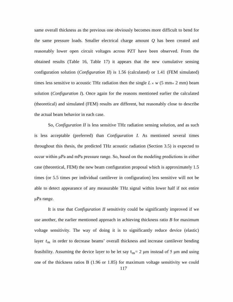
117
same overall thickness as the previous one obviously becomes more difficult to bend for
the same pressure loads. Smaller electrical charge amount Q has been created and
reasonably lower open circuit voltages across PZT have been observed. From the
obtained results (Table 16, Table 17) it appears that the new cumulative sensing
configuration solution (Configuration II) is 1.56 (calculated) or 1.41 (FEM simulated)
times less sensitive to acoustic THz radiation then the single L × w (5 mm× 2 mm) beam
solution (Configuration I). Once again for the reasons mentioned earlier the calculated
(theoretical) and simulated (FEM) results are different, but reasonably close to describe
the actual beam behavior in each case.
So, Configuration II is less sensitive THz radiation sensing solution, and as such
is less acceptable (preferred) than Configuration I. As mentioned several times
throughout this thesis, the predicted THz acoustic radiation (Section 3.5) is expected to
occur within μPa and mPa pressure range. So, based on the modeling predictions in either
case (theoretical, FEM) the new beam configuration proposal which is approximately 1.5
times (or 5.5 times per individual cantilever in configuration) less sensitive will not be
able to detect appearance of any measurable THz signal within lower half if not entire
μPa range.
It is true that Configuration II sensitivity could be significantly improved if we
use another, the earlier mentioned approach in achieving thickness ratio B for maximum
voltage sensitivity. The way of doing it is to significantly reduce device (elastic)
layer 𝑡𝑚 in order to decrease beams’ overall thickness and increase cantilever bending
feasibility. Assuming the device layer to be let say tm= 2 μm instead of 5 μm and using
one of the thickness ratios B (1.96 or 1.85) for maximum voltage sensitivity we could

118
have much more sensitive configuration with L=2 mm, w=1 mm, tm= 2 μm and tp= 1
μm (based on B). This configuration, let say for a pressure load p of 1Pa will give us an
open circuit voltage generation across PZT of V=-5.5 mV (calculated) which compared
with the initial tm=5 μm configuration generated voltage of V=-2.2 mV (Table 16) is
~2.5 times higher. It is obvious that this approach has increased cumulative configuration
sensitivity for ~2.5 times (-22.02 mV), and comparing it with Configuration I sensitivity
of V= -13.76 mV (Table 16) this configuration is ~1.6 times more sensitive and as such is
considered as preferred THz sensing solution. However, according to some overall sensor
design considerations, the cantilever physical implementation with device layer thickness
below 5μm is not currently considered as an acceptable option. Several attempts to
fabricate cantilever with device layer thickness of 5 μm failed. Thus, Configuration I still
remain preferred sensing option only based on sensor physical implementation feasibility
rather than on sensing performance.
4.4 Cross tethers sensing configuration
As stated in Section 3.6 the cross tethers sensing configuration is the last
cantilever based sensing option, the sensing performance of which has been analyzed and
investigation findings have been presented within this research work. The proposed
sensing configuration (greatly enlarged version of Figure 16 from Section 3.6) is as
shown in Figure 47 below. Besides configuration geometry the main difference between
this and previous two cantilever sensing configurations are greatly reduced PZT covering
area and tethers (beams’) movement freedom (no loose beams ends) when exposed to
pressure loads.

119
Figure 47. 3D solid model of cross tethers sensing configuration
The device design and FEM simulation modeling have been conducted in the
same fashion as it was case in previous two analyzed configurations. After initial 2-D L-
Edit© layout designs the CoventorWare® 3-D solid models have been generated, the
mesh analysis has been conducted and the adequate mesh models have been generated.
The 3-D mesh model that belong to the configuration with thickness ratio for maximum
voltage sensitivity (B=1.85) is shown in Figure 48.
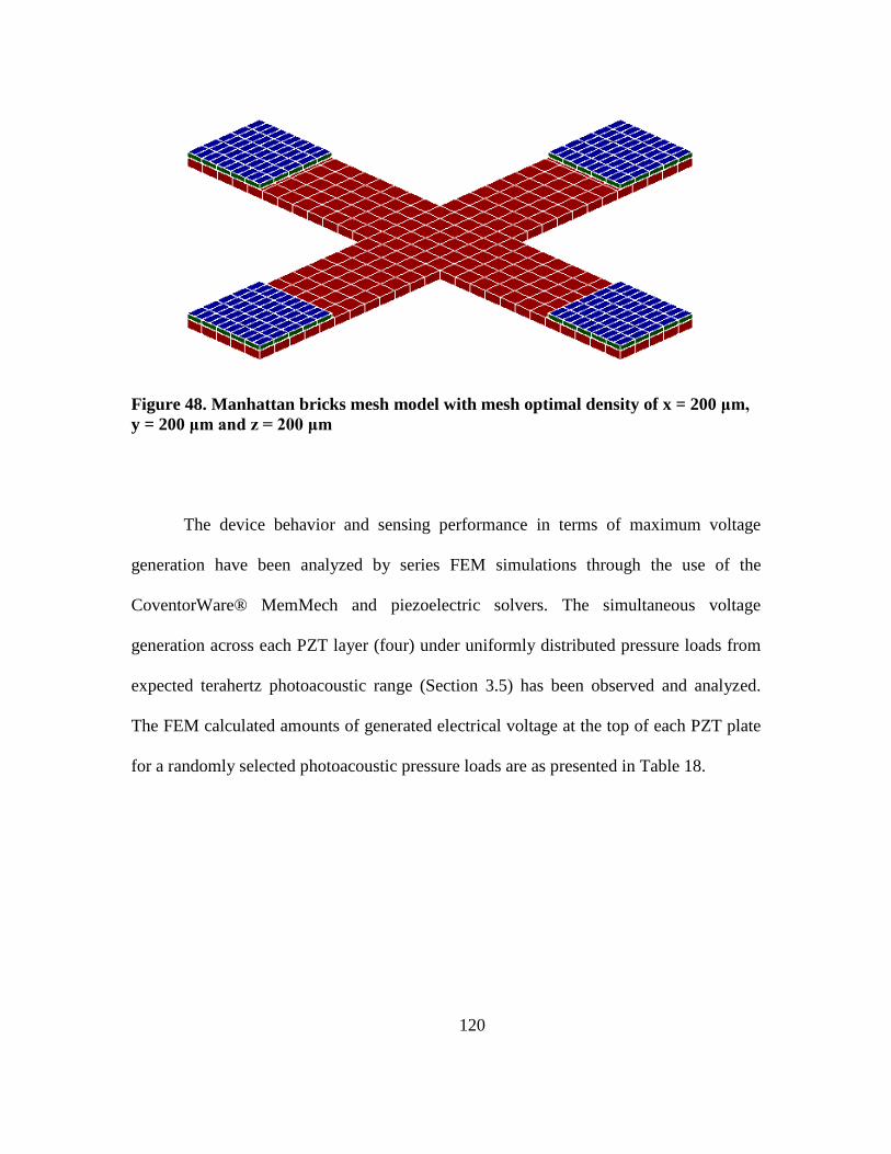
120
Figure 48. Manhattan bricks mesh model with mesh optimal density of x = 200 μm, y = 200 μm and z = 200 μm
The device behavior and sensing performance in terms of maximum voltage
generation have been analyzed by series FEM simulations through the use of the
CoventorWare® MemMech and piezoelectric solvers. The simultaneous voltage
generation across each PZT layer (four) under uniformly distributed pressure loads from
expected terahertz photoacoustic range (Section 3.5) has been observed and analyzed.
The FEM calculated amounts of generated electrical voltage at the top of each PZT plate
for a randomly selected photoacoustic pressure loads are as presented in Table 18.
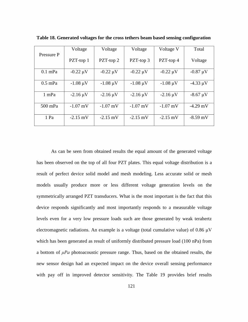
121
Table 18. Generated voltages for the cross tethers beam based sensing configuration
Pressure P Voltage
PZT-top 1
Voltage
PZT-top 2
Voltage
PZT-top 3
Voltage V
PZT-top 4
Total
Voltage
0.1 mPa -0.22 μV -0.22 μV -0.22 μV -0.22 μV -0.87 μV
0.5 mPa -1.08 μV -1.08 μV -1.08 μV -1.08 μV -4.33 μV
1 mPa -2.16 μV -2.16 μV -2.16 μV -2.16 μV -8.67 μV
500 mPa -1.07 mV -1.07 mV -1.07 mV -1.07 mV -4.29 mV
1 Pa -2.15 mV -2.15 mV -2.15 mV -2.15 mV -8.59 mV
As can be seen from obtained results the equal amount of the generated voltage
has been observed on the top of all four PZT plates. This equal voltage distribution is a
result of perfect device solid model and mesh modeling. Less accurate solid or mesh
models usually produce more or less different voltage generation levels on the
symmetrically arranged PZT transducers. What is the most important is the fact that this
device responds significantly and most importantly responds to a measurable voltage
levels even for a very low pressure loads such are those generated by weak terahertz
electromagnetic radiations. An example is a voltage (total cumulative value) of 0.86 μV
which has been generated as result of uniformly distributed pressure load (100 nPa) from
a bottom of μPa photoacoustic pressure range. Thus, based on the obtained results, the
new sensor design had an expected impact on the device overall sensing performance
with pay off in improved detector sensitivity. The Table 19 provides brief results

122
summary and comparison in sensitivity levels between this and the sensing options
analyzed in Section 4.2 and Section 4.3. The results in the last two table columns
represent the total (cumulative) voltage generation across all four symmetrically arranged
configurations’ transducers shown in Figure 43 (Section 4.3) and Figure 44 above.
Table 19. Generated voltages across PZT for three different sensing configurations
Pressure p Voltage
Configuration I
Total Voltage
Configuration II
Total voltage
Cross tethers beams
0.1 mPa -0.41 μV -0.29 μV -0.86 μV
0.5 mPa -2.05 μV -1.445 μV -4.33 μV
1 mPa -4.09 μV -2.89 μV -8.67 μV
500 mPa -1.45 mV -1.45 mV -4.29 mV
1 Pa -4.09 mV -2.89 mV -8.59 mV
The results indicate that the single rectangular shape cantilever sensor
(Configuration I) is approximately about 30% more sensitive than Configuration II but
52% less sensitive than cross tethers sensing option. So, the cross tethers (beams) based
configuration in terms of maximum voltage sensitivity performs much better than the
CoventorWare® MemMech other two previously analyzed options.
Furthermore, using solver the modal analysis of the structure has been performed.
The aim of this analysis was to investigate the device mechanical response (deformation
modes) under uniformly distributed photoacoustic pressure loads and to calculate the

123
natural resonant frequencies associated with each modal shape. The investigation results
have indicated which mode will ensure maximum device response based on its
displacements and consequently the maximum amount of electrical charge generation as
result of induced stress in device x, y, and z directions. The analysis has been performed
for the very low 100Hz to 1600Hz harmonic frequency range on the 10mPa pressure-
loaded tethers configuration with requested 10 frequencies display. The device is
examined for various mode shapes and its resonant frequencies have been determined
accordingly. The obtained results for each modal shape are shown in Table 20.
Table 20. Calculated resonant frequencies for cross tethers beam configuration
Modes Mode 1 Mode 2 Mode 3 Mode 4 Mode 5 Mode 6
Resonant
frequencies 2.01 kHz 4.32 kHz 4.33 kHz 6.23 kHz 7.89 kHz 10.12 kHz
Once again it has been found that Mode 1 impact on the device response is much
higher than are impacts of the other modal shapes. The resulting vibrating pattern (greatly
enlarged) of this mode and its generalized displacement response as a function of
frequency is presented in Figure 49 and Figure 50. The remaining mode shapes of
vibrating pattern with associated resonant frequencies and generalized displacements
response can be seen in Appendix B.
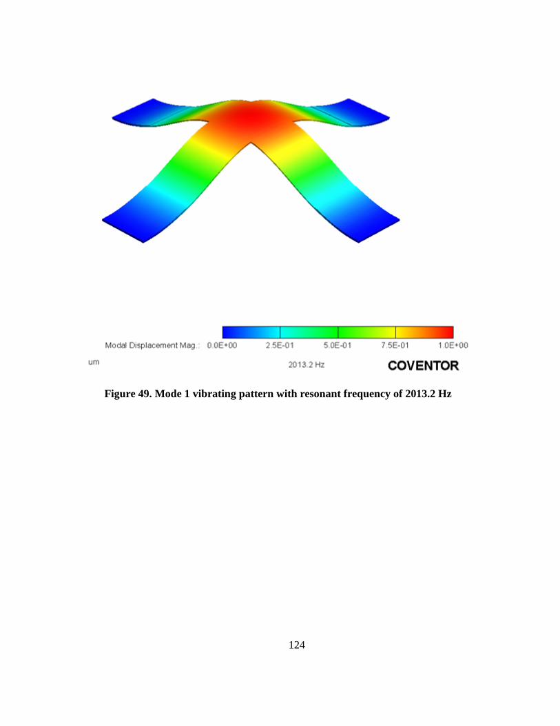
124
Figure 49. Mode 1 vibrating pattern with resonant frequency of 2013.2 Hz
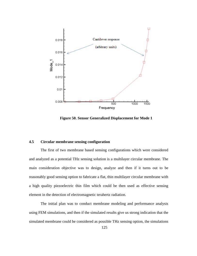
125
Figure 50. Sensor Generalized Displacement for Mode 1
4.5 Circular membrane sensing configuration
The first of two membrane based sensing configurations which were considered
and analyzed as a potential THz sensing solution is a multilayer circular membrane. The
main consideration objective was to design, analyze and then if it turns out to be
reasonably good sensing option to fabricate a flat, thin multilayer circular membrane with
a high quality piezoelectric thin film which could be then used as effective sensing
element in the detection of electromagnetic terahertz radiation.
The initial plan was to conduct membrane modeling and performance analysis
using FEM simulations, and then if the simulated results give us strong indication that the
simulated membrane could be considered as possible THz sensing option, the simulations
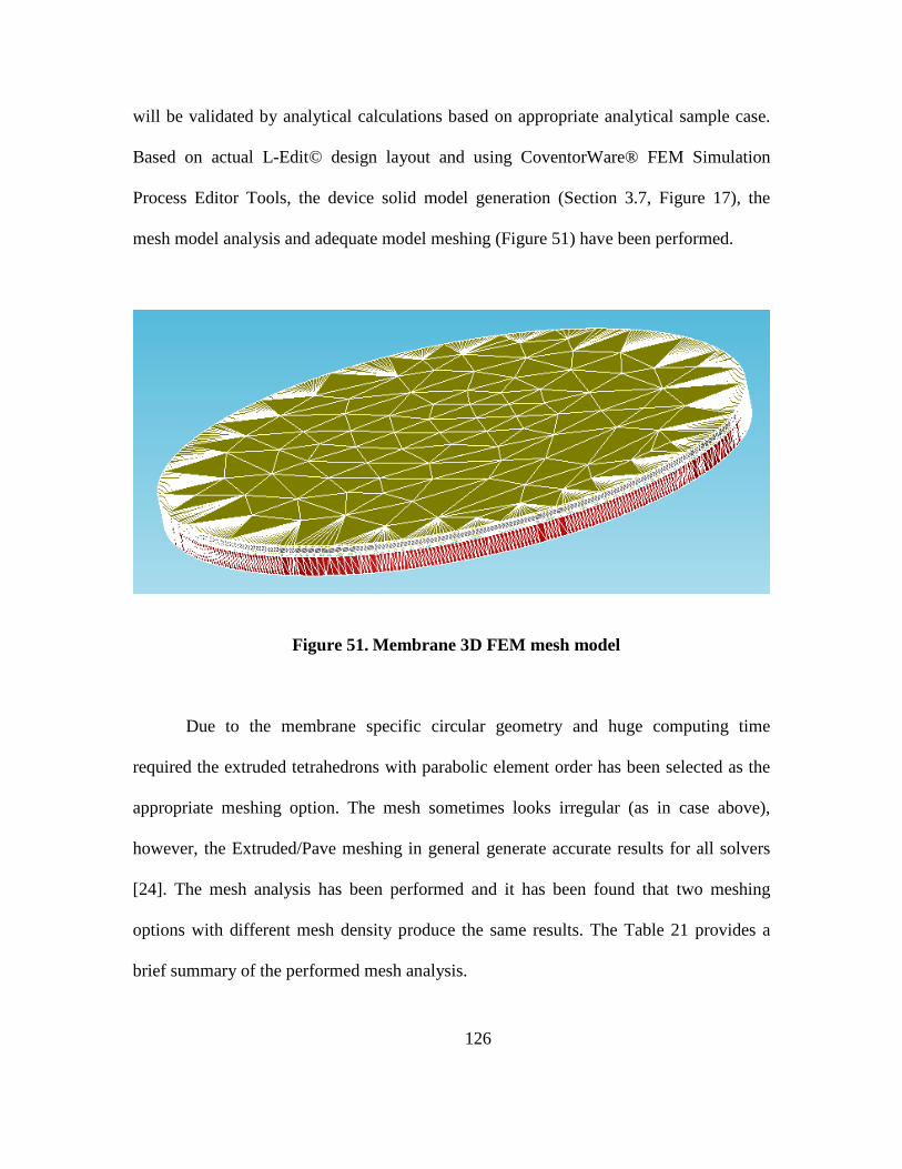
126
will be validated by analytical calculations based on appropriate analytical sample case.
Based on actual L-Edit© design layout and using CoventorWare® FEM Simulation
Process Editor Tools, the device solid model generation (Section 3.7, Figure 17), the
mesh model analysis and adequate model meshing (Figure 51) have been performed.
Figure 51. Membrane 3D FEM mesh model
Due to the membrane specific circular geometry and huge computing time
required the extruded tetrahedrons with parabolic element order has been selected as the
appropriate meshing option. The mesh sometimes looks irregular (as in case above),
however, the Extruded/Pave meshing in general generate accurate results for all solvers
[24]. The mesh analysis has been performed and it has been found that two meshing
options with different mesh density produce the same results. The Table 21 provides a
brief summary of the performed mesh analysis.

127
Table 21. Membrane deflection response to uniformly distributed pressure loads
Element size 1000 μm Element size 600 μm Element size 300 μm
Pressure p Deflection ‘z’ Deflection ‘z’ Deflection ‘z’
1μPa -2.7e-11 μm -5.3e-11 μm -5.3e-11 μm
1mPa -2.7e-8 μm -5.3e-8 μm -5.3e-8 μm
1Pa -2.7e-3 μm -5.3e-3 μm -5.3e-3 μm
From the obtained results it can be seen that the two meshes (minimum
requirement) with parabolic element order and element size in planar direction of 600 μm
and 300 μm and 5 μm in extruded direction, generate essentially the same deflection
results; therefore, the model can be considered mathematically accurate. Due to the
significant difference in computing time the mesh model with mesh density involving
element size of 600 μm in planar and 5 μm in extruded direction has been used
throughout entire model simulation and testing process.
The initial FEM simulations and analysis have been firstly performed on the
standard, then on the reduced in thickness membrane configurations. Standard manly
refers to the membrane model implemented on a 100 mm Silicon On Insulator (SOI)
wafer with device and piezoelectric layer thickness of 5 μm and 2.7 μm (B=1.87)
respectively. So, the model with an overall membrane thickness of 8 μm (including SiO2
and two metal layers) has been exposed to the expected THz photoacoustic pressure
range (1μPa - 1Pa). After the performed simulations it has been found out that the
membrane does not respond to the prescribed acoustic pressure levels at all. Due to the

128
relatively high overall thickness and the fact that the membrane has been entirely fixed all
around its circumference the applied loads have not been able to produce any significant
device deformation or any deformation at all. Just as an illustration of the membranes
insensitivity, here are a few deflection results (Table 22) related to the pressure loads of
10 Pa, 20 Pa and 40 Pa, respectively.
Table 22. Membrane deflections for maximum voltage sensitivity configuration (B=1.85) for tm=5 μm and tp=2.7 μm
Pressure p Deflection z
10 Pa - 0.53 nm
20 Pa -1.06 nm
40 Pa -2.2 nm
The typical 3D FEM simulation result of the piezoelectric membrane simulations
is presented in Figure 52.

129
Figure 52. FEM simulation result of circular membrane for a pressure load of 10 Pa
As can be noticed, due to negligible membrane deflection, even for a uniformly
distributed pressure load of 10 Pa, the visible sensing deformation could not be observed
without huge simulation enlargement, as shown in the following figure (Figure 53).

130
Figure 53. Enlarged FEM simulation result of circular membrane for a pressure load of 10 Pa
From the obtained results, even for simulations related to pressure loads that are
well outside the THz photoacoustic range, there is no indication of any electric charge
and voltage generation. Based on presented, the observed membrane configuration with
an overall thickness of 8μm, without a question, is not a sensing solution that we are
looking for. In respect to all these, it is obvious that if we want a membrane as integrated
open circuit sensing solution, in that case the membrane must a be really thin device with
a high quality PZT. Furthermore, as an attempt, and of course as a part of research work,
in order to get an estimation insight into thin membranes’ sensitivity levels, and how far
we can go in membranes’ thickness decrease, another so called reduced model membrane

131
(reduced in thickness) has been designed, simulated and investigated. Due to some
considerations associated with the sensor physical implementation feasibility it is still
unknown (testing required) how far below 5 μm we can go in device layer thickness
decrease. With respect to that, in order to analyze a reasonably feasible thin membrane
and to observe its sensitivity level the tm =1.5 μm has been randomly selected. So, based
on the FEM thickness ratio (1.85) for a maximum voltage sensitivity, the membrane
configuration with an overall thickness of 2.6μm (tm =1.5 μm, tp=0.8 μm, SiO2 and metal
layers 0.1 μm) has been investigated. The selected portion of obtained results for selected
pressure loads of 1 Pa, 5 Pa and 10 Pa are as presented in Table 23.
Table 23. Membrane deflections and corresponding voltage response in a case of reduced thickness configuration (B=1.85) with tm=1.5 μm and tp=0.8 μm
Pressure p Deflection z Generated V
1 Pa -0.1 nm -0.029 μV
5 Pa -0.51 nm -0.15 μV
10 Pa -1 nm -0.29 μV Once again the obtained results show that membrane even with a decrease in
overall thickness of almost three times in comparison with previous version is not
sensitive enough to be able to detect any measurable signal from THz radiation range.
The reason for membrane sensing inefficiency, as already pointed out, is due to the fact
that the membrane in contrast to cantilever (one or both sides fixed) is fully fixed around
entire circumference. As a result, as observed, much higher pressure levels are required to

132
produce the same deflections in “z” direction, and consequently to cause the same
piezoelectric deformation in the membrane edge areas, where the electrical charge in fact
is going to be generated. Thus, based on observed device insensitivity the membrane as
such should not be considered as potential terahertz sensing option.
In addition to all that has been said above in relation to the circular membrane
insensitivity, Appendix C contains FEM results related to membrane Modal and the
Mises Stress analysis which give a deeper insight into the behavior of the membrane
under uniformly distributed photoacoustic pressure loads.
4.6 Square membrane sensing configuration
This section presents a brief FEM investigation summary of the square membrane
sensing configuration. Its L-Edit© design layout and the generated 3-D solid model are
shown in Figure 18 and Figure 19 (Section 3.7) respectively. Due to the device specific
geometry the extruded bricks with parabolic element order has been selected as the
appropriate meshing model. The mesh analysis has been conducted and the adequate
mesh model has been generated, which can be seen in Figure 54.
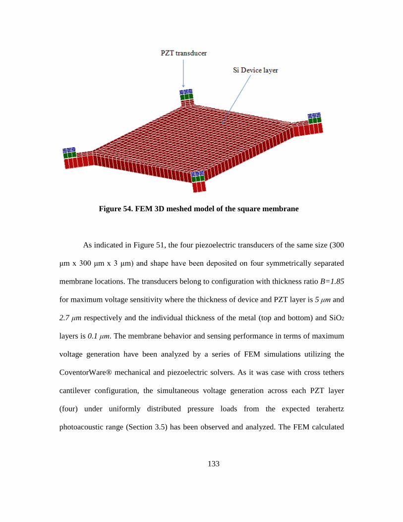
133
Figure 54. FEM 3D meshed model of the square membrane
As indicated in Figure 51, the four piezoelectric transducers of the same size (300
μm x 300 μm x 3 μm) and shape have been deposited on four symmetrically separated
membrane locations. The transducers belong to configuration with thickness ratio B=1.85
for maximum voltage sensitivity where the thickness of device and PZT layer is 5 μm and
2.7 μm respectively and the individual thickness of the metal (top and bottom) and SiO2
layers is 0.1 μm. The membrane behavior and sensing performance in terms of maximum
voltage generation have been analyzed by a series of FEM simulations utilizing the
CoventorWare® mechanical and piezoelectric solvers. As it was case with cross tethers
cantilever configuration, the simultaneous voltage generation across each PZT layer
(four) under uniformly distributed pressure loads from the expected terahertz
photoacoustic range (Section 3.5) has been observed and analyzed. The FEM calculated
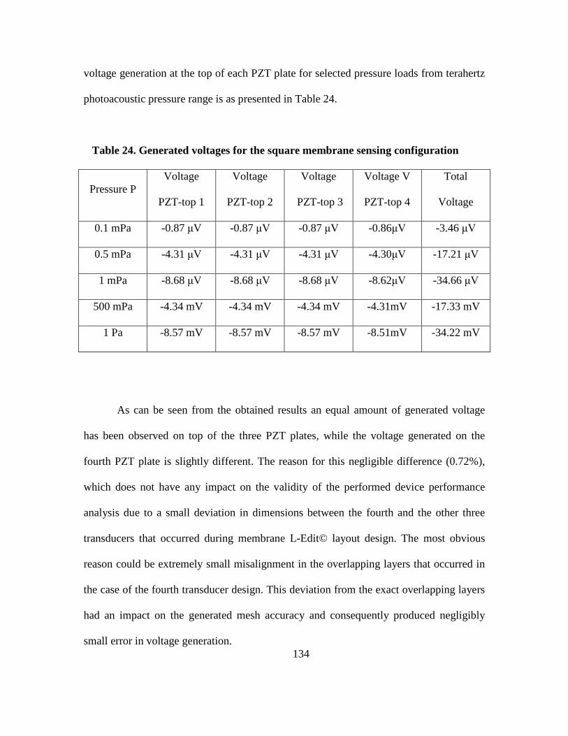
134
voltage generation at the top of each PZT plate for selected pressure loads from terahertz
photoacoustic pressure range is as presented in Table 24.
Table 24. Generated voltages for the square membrane sensing configuration
Pressure P Voltage
PZT-top 1
Voltage
PZT-top 2
Voltage
PZT-top 3
Voltage V
PZT-top 4
Total
Voltage
0.1 mPa -0.87 μV -0.87 μV -0.87 μV -0.86μV -3.46 μV
0.5 mPa -4.31 μV -4.31 μV -4.31 μV -4.30μV -17.21 μV
1 mPa -8.68 μV -8.68 μV -8.68 μV -8.62μV -34.66 μV
500 mPa -4.34 mV -4.34 mV -4.34 mV -4.31mV -17.33 mV
1 Pa -8.57 mV -8.57 mV -8.57 mV -8.51mV -34.22 mV
As can be seen from the obtained results an equal amount of generated voltage
has been observed on top of the three PZT plates, while the voltage generated on the
fourth PZT plate is slightly different. The reason for this negligible difference (0.72%),
which does not have any impact on the validity of the performed device performance
analysis due to a small deviation in dimensions between the fourth and the other three
transducers that occurred during membrane L-Edit© layout design. The most obvious
reason could be extremely small misalignment in the overlapping layers that occurred in
the case of the fourth transducer design. This deviation from the exact overlapping layers
had an impact on the generated mesh accuracy and consequently produced negligibly
small error in voltage generation.

135
However, the most important observation is that this device with a significant
change in configuration geometry exhibits tremendously high voltage sensitivity level
like no one of the sensing options whose sensing performance have been discussed in this
research work. Just as an illustration (Table 24) of its high sensitivity is a voltage
generation of even 3.46 μV (cumulative value) as a response to uniformly distributed
pressure load (100 nPa) from a very bottom of μPa photoacoustic pressure range. Having
in mind the estimated terahertz photoacoustic pressure loads, ranging between μPa and
mPa pressure levels (Section 3.5), this level of detector sensitivity is exactly what we are
looking for. Based on the obtained results there is no doubt that a square membrane
sensing configuration will be able to detect weak THz electromagnetic radiation.
The Table 25 provides brief results summary and comparison in sensitivity levels
between the square membrane and other two out of the four remaining analyzed sensing
configurations, which were among the options with achieved better sensitivity results.
Table 25. Generated voltages across PZT for three different sensing configurations
Pressure p Voltage V
Configuration I
Total voltage V
Cross tethers beams
Total voltage V
Square membrane
0.1 mPa -0.41 μV -0.86 μV -3.46 μV
0.5 mPa -2.05 μV -4.33 μV -17.22 μV
1 mPa -4.09 μV -8.67 μV -34.66 μV
500 mPa -1.45 mV -4.29 mV -17.33 mV
1 Pa -4.09 mV -8.59 mV -34.22 mV

136
The presented results clearly show that all three sensing configurations have
demonstrated the ability to respond effectively to any pressure load from entire terahertz
photoacoustic radiation range. These results indicate that the square membrane sensing
performance is by far superior compared to the other two solutions, exhibiting by
approximately about four times more sensitivity than the configuration involving cross
tethers beams, and more than eight times more sensitivity than Configuration I.
As it was case with any of the previous configuration investigations, FEM
simulations were also performed on square membrane in order to determine its resonance
frequency and mechanical vibration mode patterns. The resulting vibrating pattern for the
first six modes and associated resonant frequencies for a pressure load of 10 mPa and
harmonic frequency range from 100 Hz to 1600 HZ is shown in Figure 55.

137
Mode 1 (1246.03 Hz) Mode 2 (2805.52 Hz)
Mode 3 (2806.17 Hz) Mode 4 (3734.37 Hz)
Mode 5(5869.87 Hz) Mode 6 (7046.84 Hz)
Figure 55. Resulting vibrating pattern and resonant frequencies for a load of 10 mPa
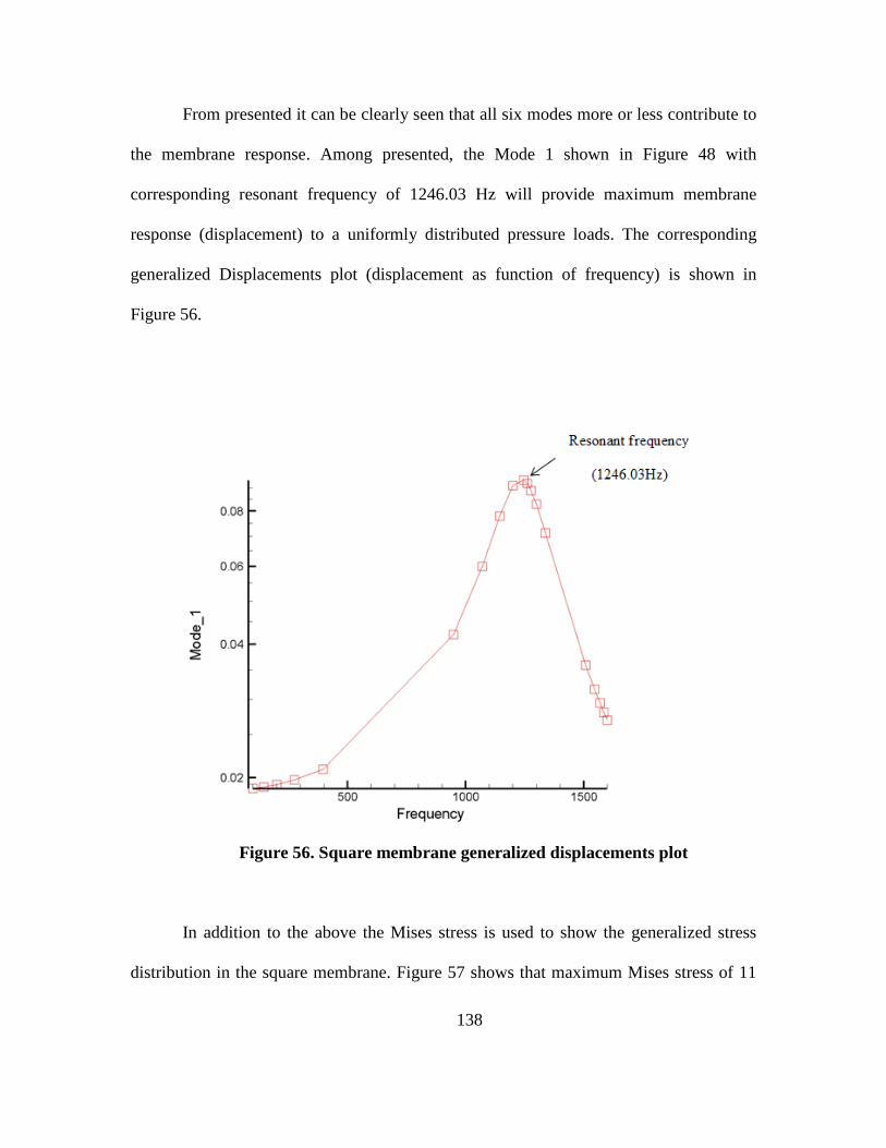
138
From presented it can be clearly seen that all six modes more or less contribute to
the membrane response. Among presented, the Mode 1 shown in Figure 48 with
corresponding resonant frequency of 1246.03 Hz will provide maximum membrane
response (displacement) to a uniformly distributed pressure loads. The corresponding
generalized Displacements plot (displacement as function of frequency) is shown in
Figure 56.
Figure 56. Square membrane generalized displacements plot In addition to the above the Mises stress is used to show the generalized stress
distribution in the square membrane. Figure 57 shows that maximum Mises stress of 11

139
kPa is concetrated outside the 0.3 µm x 0.3 µm PZT coverage ares. In order to maximize
configuration response (increase sensitivity) as part of FEM sensor optimization the PZT
sensing area has been increased from 0.3 µm x 0.3 µm to 0.52 µm x 0.52 µm in order to
cover membranes’ areas where Mises stress is most pronaunced. However, the expected
increase in voltage sensitivity has not been achived. The obtained results in Apendix D
shows that an increase in PZT area did not provide expected sensitivity increase so, the
previous sensing geometry with PZT area of 0.3 µm x 0.3 µm is still prefered sensing
option. The reason for this is that maximum Mises stress will always occur just below
PZT ares where silicon membrane is thiner while the effective bending in PZT covered
areas will happened close to the fixed membranes ends. The obtained results for voltage
generation of this optimization attempt for rendomly selected photoacoustic pressure
loads and their comparison with configuration results involving 0.3 µm x 0.3 µm PZT
transducers are presented in Appendix D.
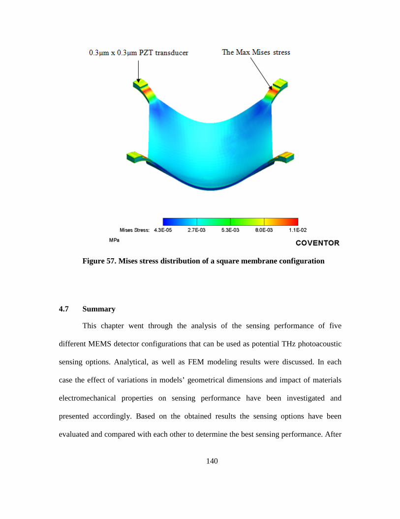
140
Figure 57. Mises stress distribution of a square membrane configuration
4.7 Summary
This chapter went through the analysis of the sensing performance of five
different MEMS detector configurations that can be used as potential THz photoacoustic
sensing options. Analytical, as well as FEM modeling results were discussed. In each
case the effect of variations in models’ geometrical dimensions and impact of materials
electromechanical properties on sensing performance have been investigated and
presented accordingly. Based on the obtained results the sensing options have been
evaluated and compared with each other to determine the best sensing performance. After

141
the conducted investigations, it has been discovered that there is some level of
disagreement between theoretical (calculated) and FEM simulated results. The possible
reasons and justification for the observed disagreement have been discussed within
relevant chapter sections. According to the obtained results, the square membrane is the
best terahertz photoacoustic sensing solution. Compared to the others, the square
membrane has demonstrated the ability to respond effectively to any radiation level from
the entire THz photoacoustic range, while exhibiting tremendously high sensitivity. In
addition to the square membrane, the cross tethers beam configuration has demonstrated
reasonable high sensing performance, being able to respond significantly well with a
significant measurable voltage response. The remaining configurations have
demonstrated much lower sensitivities and inability to effectively cover the entire THz
photoacoustic range or even to demonstrate almost any ability to respond to any
photoacoustic pressure input.
V. Conclusions and Recommendations
The objective of this research work was to design and develop a novel
photoacoustic detector responsive to sub-millimeter/terahertz radiation. Due to the nature
of the proposed research activity, many different terahertz sensing configurations were
designed and analyzed. Initially, when the research began, it was not clear what the
expected detector functionality was and which MEMS based sensing configuration would
respond effectively and which would not; however, at this stage it is possible to draw

142
some conclusion about the outcomes, whether positive or negative, and based on these
recommendations can be made.
5.1 Conclusions
The expected outcome of this research is a terahertz photoacoustic detection that
may lead to the development of the hand held THz chemical sensors and THz detector
arrays for imagining. Besides a number of other components that will be used to build a
photoacoustic system, there is a requirement for the development of highly sensitive
detector as the vital part of the intended terahertz photoacoustic sensor design. Based on
the fact that THz electromagnetic radiation is a very short and weak pulse emission, the
feasibility of its detection is seen in the utilization of MEMS cantilever-based sensors.
This research has gone through the whole process of detector development with the main
focus on sensor analytical and FEM modeling. Initially, based on L-Edit© detector
surface modeling designs and fully developed device fabrication process, several
cantilever sensing configurations have been intended to be fabricated and tested. The
observed sensing performance was to be compared with analytical and simulated results.
This research modeled five different detector configurations whose sensing performance
has been evaluated, assessed and compared among each other. In each case, the effect of
variations in the models’ geometrical dimensions and impact of materials’
electromechanical properties on sensing performance has been investigated. After
conducted investigations, it has been determined that the square membrane sensing
performance is by far superior compared to the other solutions and as such is
recommended as the preferred terahertz sensing option.
143
5.2 Recommendations
After completion of this investigation there are many recommendations that can
be made. Some of them are obvious and already have been more or less recognized and
stated within relevant thesis sections. First of all, during this research work several
sensing configurations have been developed whose sensing performance have been
assessed by analyzing the collections of analytical and simulated data results. Some of the
configurations have been identified as potential terahertz sensing solution while some are
not. Hence, to confirm assessment validity, verify and evaluate configurations that have
been identified as potential sensing option the fabrication and actual device sensitivity
measurements and comparison with simulated results would be required. Furthermore,
based on the requirement for the development of highly sensitive MEMS based detector,
responsive to a weak terahertz electromagnetic radiation in order to improve its
sensitivity the modeling and sensing performance analysis of cantilever based sensing
configurations involving double piezoelectric layer would be one possibility for
improvement. This research work has been focused on the sensing options with single
piezoelectric layer configurations, however based on some published research results [13]
the use of double layer configurations with the same geometrical dimensions could
significantly improve detectors sensitivity. Another recommendation could be to conduct
an investigation related to device layer thickness decrease. From the sensor physical
implementation point of view it is still unknown how far below 5μm device layer
thickness it is possible to go. As mentioned earlier, several attempts of fabricating
cantilever with 5μm device layer failed; hence, in order to determine the reason of failure
and thin device layer fabrication feasibility an investigation into material properties and

144
fabrication process would be required. A sensing configuration with defined thickness
ratio for maximum voltage sensitivity involving thinner device layer would increase
detector sensitivity significantly as discussed and presented in Chapter IV. Besides the
recommendations related to detector sensing performance improvement there is always
room for sensor optimization options which mainly involve investigation in new
configuration shape (geometry), optimal piezoelectric coverage area or possibility of
using materials with different electromechanical properties. The last mentioned
recommendation would be required especially in the case of MEMS membrane-based
sensing configurations development, where thickness, shape and membranes’ elasticity
are main factors that define detectors sensing performance.
5.3 Contributions
Some valuable contributions were made in the completion of this research work. These
contributions are listed below.
- The thickness ratio B for maximum voltage sensitivity has been observed and
as such can be used as a valid data in the future cantilever sensing
configurations designs involving Si and PZT materials as main device
structural layers.
- Two out of five developed sensing configurations, namely cross tethers and
square membrane sensing configurations are unique sensing options which
have demonstrated high sensitivity level and as such with a further

145
optimization can be thought as a possible THz radiation sensing solutions for
a detector in development.
- This research modeled five different sensing configurations with full L-Edit
design layouts and FEM simulation results for the voltage generation across
PZT sensing elements for the entire estimated terahertz photoacoustic pressure
range. Based on the obtained results future work may require only device
fabrication, its testing and obtained test results comparison with the already
provided simulated results.

146
Appendix A
A-1 THz Photoacoustic Cantilever Fabrication Procedures

147

148

149

150

151
152

153

154
A-2 Configuration I CoventorWare® Process Editor Fabrication Process
Step No: 0
Step No: 1
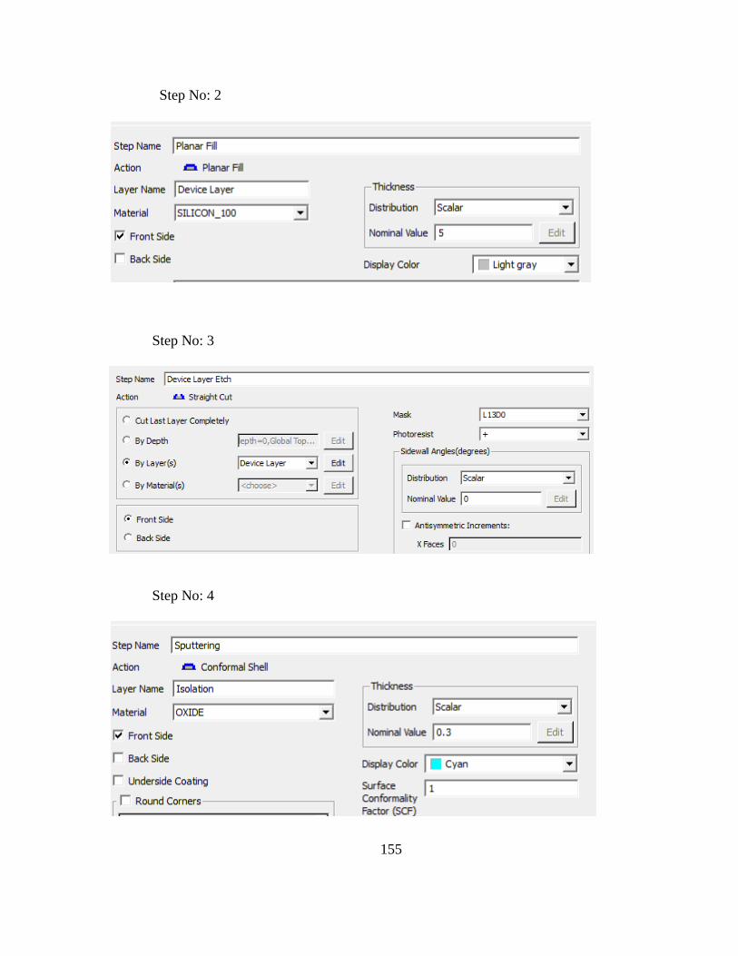
155
Step No: 2
Step No: 3
Step No: 4

156
Step No: 5
Step No: 6
Step No: 7
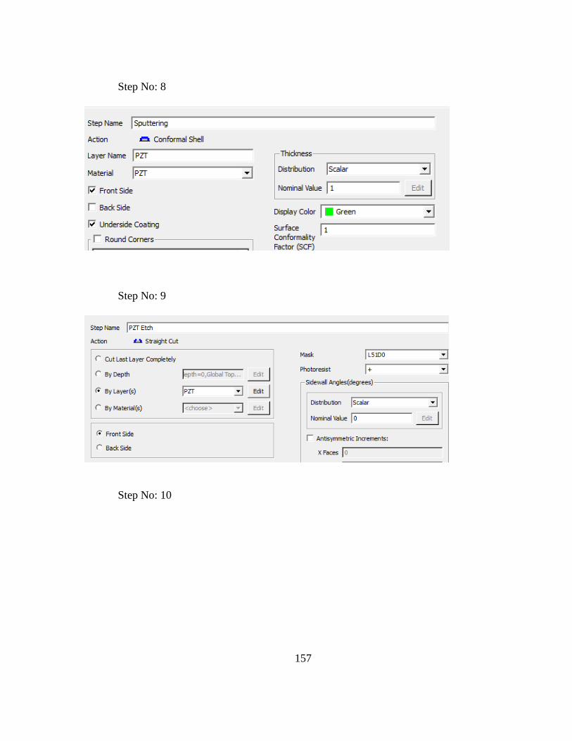
157
Step No: 8
Step No: 9
Step No: 10

158
Step No: 11
Step No: 12
Step No: 13

159
A-3 List of material properties used in the analytical and FEM modeling
- Si <100> Young’s modulus E = 130.18 GPa - PZT Young’s modulus E = 89 GPa - Gold Young’s modulus E = 57 GPa - Platinum Young’s modulus E = 145 GPa - Transverse piezoelectric coefficient d31 = 274e-12 m/V - Electromechanical coupling coefficient k31 = 0.344 - Dielectric constant of the piezoelectric material under free conditions; ε˟₃₃ = 1700 F/m

160
Appendix B
B-1 Cross Tethers CoventorWare® Process Editor Fabrication Process
Step No: 0
Step No: 1
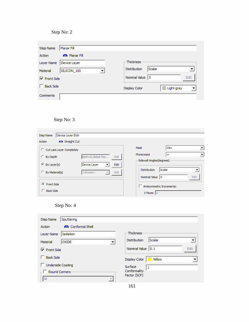
161
Step No: 2
Step No: 3
Step No: 4

162
Step No: 5
Step No: 6
Step No: 7
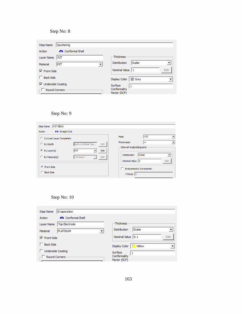
163
Step No: 8
Step No: 9
Step No: 10

164
Step No: 11
Step No: 12
Step No: 13
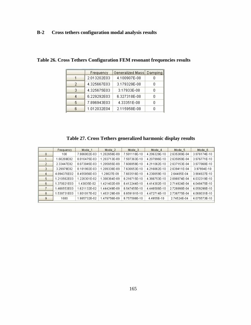
165
B-2 Cross tethers configuration modal analysis results
Table 26. Cross Tethers Configuration FEM resonant frequencies results
Table 27. Cross Tethers generalized harmonic display results
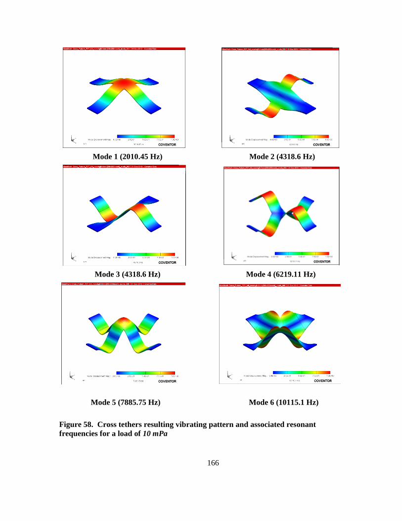
166
Mode 1 (2010.45 Hz) Mode 2 (4318.6 Hz)
Mode 3 (4318.6 Hz) Mode 4 (6219.11 Hz)
Mode 5 (7885.75 Hz) Mode 6 (10115.1 Hz) Figure 58. Cross tethers resulting vibrating pattern and associated resonant frequencies for a load of 10 mPa
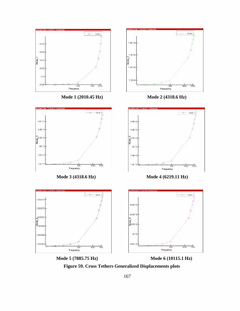
167
Mode 1 (2010.45 Hz) Mode 2 (4318.6 Hz)
Mode 3 (4318.6 Hz) Mode 4 (6219.11 Hz)
Mode 5 (7885.75 Hz) Mode 6 (10115.1 Hz) Figure 59. Cross Tethers Generalized Displacements plots

168
Appendix C
C-1 Circular Membrane CoventorWare® Process Editor Fabrication Process
Step No: 0
Step No: 1

169
Step No: 2
Step No: 3
Step No: 4

170
Step No: 5
Step No: 6
Step No: 7

171
C-2 Circular Membrane FEM Modal and Mises Stress analysis results
As mentioned in Section 4.5 the additional results presented in this appendix
section provide a deeper insight into circular membrane insensitivity. As can be seen in
Table 29 that depict modal analysis results, membrane (with overall thickness of 2. 6μm)
does not respond at all even for photoacoustic pressure load of 5 Pa. Responses
associated with Mode 3, Mode 4, and Mode 6 is clearly zero while response associated
with remaining modes are well below measurable levels. The same observations can be
seen from Figure 57 and Figure 58.
Table 28. Circular membrane FEM natural resonant frequencies results
Table 29. Circular membrane generalized harmonic display results
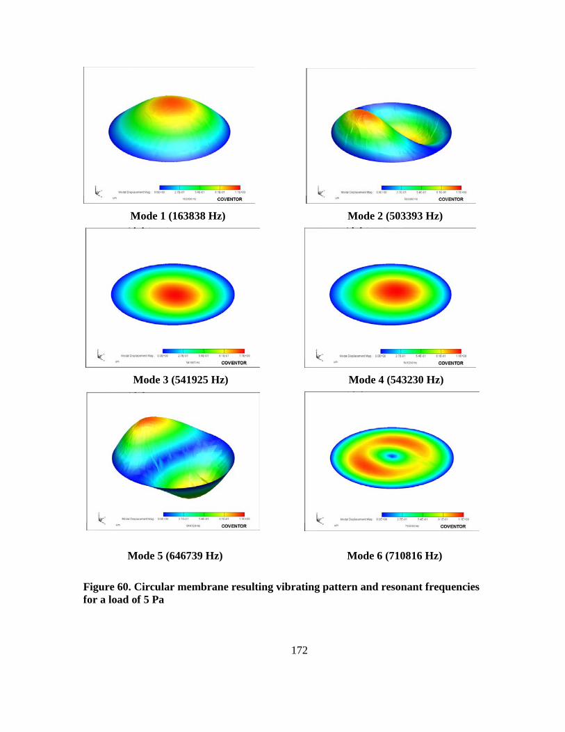
172
Mode 1 (163838 Hz) Mode 2 (503393 Hz)
Mode 3 (541925 Hz) Mode 4 (543230 Hz)
Mode 5 (646739 Hz) Mode 6 (710816 Hz) Figure 60. Circular membrane resulting vibrating pattern and resonant frequencies for a load of 5 Pa

173
Mode 1 (163838 Hz) Mode 2 (503393 Hz)
Mode 3 (541925 Hz) Mode 4 (543230 Hz)
Mode 5 (646739 Hz) Mode 6 (710816 Hz)
Figure 61. Circular Membrane Generalized Displacements plots

174
Figure 62. FEM model result of the deflection of a clamped circular membrane for 5 Pa photoacoustic load. As can be seen in Figure 62 the maximum deflection of 5.1μm occurs at the
center of membrane. The figure also shows that the deflection at fixed boundary (red
color) between the membrane and the surrounding silicon frame is only 0.83nm. This
deflection in critical stress area is so small that will not create any effective stress and
charge generation at all as explained in Section 4.5. Furthermore, Figure 63 below, which
is FEM Mises stress representation, clearly indicates that there is no radial and tangential
stress generation as result of uniformly distributed pressure load.

175
Figure 63. Circular Membrane FEM Mises stress distribution for 5 Pa photoacoustic pressure load

176
Appendix D
D-1 Square Membrane CoventorWare® Process Editor Fabrication Process
Step No: 0
Step No: 1

177
Step No: 2
Step No: 3
Step No: 4

178
Step No: 5
Step No: 6
Step No: 7

179
Step No: 8
Step No: 9
Step No: 10

180
D-2 Square Membrane FEM results for 0.52 µm x 0.52 µm PZT transducers
Figure 64. FEM 3D meshed model of the square membrane (Extruded bricks, element order parabolic, element size in planar direction 200, element size in extrude direction 5)

181
Table 30. Generated voltages for the square membrane sensing configuration involving PZT transducers of 0.3 µm x 0.3 µm and 0.52 µm x 0.52 µm
Figure 65. Square membrane deflection for 10mPa uniformly distributed pressure load

182
Figure 66. Mises stress distribution of a square membrane configuration involving 0.52 µm x 0.52 µm PZT transducers

183
Bibliography
[1] F. C. De Lucia, “Spectroscopy in the Terahertz Spectral Region, “in Sensing with Terahertz Radiation, D. Mittleman, Ed. Berlin: Springer, 2003 pp. 39-116.
[2] Daniel Mittleman, “Sensing with Terahertz Radiation,” Springer-Verlag, Berlin Hilderberg, 2003.
[3] Frank C. De Lucia, “Terahertz Spectroscopy and Applications, “in Proceedings IEEE International Symposium on Frequency Control, 1-8, 2006.
[4] Andreas Mandelis, “Photoacoustic and Thermal Wave Phenomena in Semiconductors,” Elsevier Science Publishing C. Inc., New York, 1987.
[5] Peter H. Sigel, “Terahertz Technology,” Invited Paper IEEE, 2003.
[6] John F Federici, Brian Schulkin, Feng Huang, Dale Gary, Robert Barat, Filipe Oliviera and David Zimdars, “THz imaging and sensing for security applications-explosives, weapons and drugs, “Semiconductor Science and Technology, 20 S266-S280, 2005.
[7] Ki Bang Lee, “Principles of Microelectromechanical Systems,” John Wiley and Sons, Inc., Indianapolis, Indiana, 1966.
[8] John Potter Shields, “Basic Piezoelectricity,” Howard W. Sams and Co.,, Inc., Hoboken, New Jersey, 2011.
[9] Larry L Altgilbers, Jason Baird, Bruce L Freeman, Christopher S Lynch, Sergey I Shkuratov, “Explosive Pulsed Power, “Imperial College Press 57 Shelton Street Covent Garden, London WC2H 9HE, 2011.
[10] Chang Liu, “Foundations of MEMS,” Pearson Prentice Hall, Upper Saddle River, New Jersey, USA, 2006.
[11] Joseph C Doll and Beth L Pruitt, “Design of piezoresistive versus piezoelectric contact mode scanning probes,” Journal of Micromechanics and Microengineering. 20 (2010) 095023 (15pp), 17 August 2010.
184
[12] Barlian A. A, Park W T, Mallon J R, Rastegar A J and Pruiitt B L, “ Semiconductor piezoresistance for microsystems,” IEEE 97 513, Volume 97,Issue 3, 2009.
[13] Qing-Ming Wang, Xiao-hong Du, Baomin Xu, and L. Eric Cross “Theoretical analysis of the sensor effect of cantilever piezoelectric benders,” Intercollege Materials Research Laboratory, Pennsylvania, 13 October 1998.
[14] Jan G. Smits and Wai-s Choihing“The Constituent Equations of Piezoelectric Heterogeneous Bimorphs,” College of Engineering, Boston University, IEEE Transactions on Ultrasonic, Ferroelectrics, and Frequency Control, Vol. 393, May 1991.
[15] Robert H. Swendsen, “An introduction to statistical mechanics and thermodynamics,” Oxford University Press, 2012.
[16] Frederic P. Miller, Agnes F. Vandome, John McBrewester, “Beer-Lambert law,” Alphascript Publishing, 11 April 2009.
[17] Tom Kuusela and Jyrki Kauppinen, “Photoacoustic Gas Analysis Using Interferometric Cantilever Microphone,” Taylor and Francis Group, LLC, ISSN 0570-492, 24 April 2007.
[18] G. West, J. Barrett, D. Siebert, “Photoacoustic spectroscopy, “Review of Scientific Instruments, 54 (1983) 797-817.
[19] Nathan Glauvitz, Stjepan Blazevic, Ronald A. Coutu Jr., Michael Kistler, Ivan R. Medvedev, Douglas T. Petkie, “MEMS photoacoustic detector of THz radiation for chemical sensing,” The 26th European Conference on Solid-State Transducers, Krakow, Poland, 10 September 2012.
[20] Bell D J, Lu T J, Fleck N A and Spearing S M, “MEMS actuators and sensors: observations and their performance and selection for purpose,” Journal of Micromechanics and Microengineering, 15 S153, 2005.
[21] Vahid Mohammadi, Mohammad Hossein Sheikhi,“Design, Modeling and Optimization of a Piezoelectric Pressure Sensor based on a Thin-Film PZT Membrane Containing Nanocrystalline Powders,” Sensors and Transducers Journal, Vol. 110,Issue 11, November 2009, pp. 56-70

185
[22] Woon Seob Lee, Seung S. Lee, “Piezoelectric microphone built on circular diaphragm, “Science Direct, Sensors and Actuators A 144 367-373, 14 February 2008.
[23] Joshi Abhay, “Design of Piezoelectric PZT Cantilever for Actuator Application,” Sensors and Transducers, 1 December 2010.
[24] CoventorWare® 2010, MEMS Design and Analysis Tutorials, Vol. 1, Vol.2.
[25] Lee.Y.-S., “Principles of Terahertz Science and Technology, Springer-Verlag US, 2009.
[26] Ikeda, I. “Fundamentals of piezoelectricity,” Oxford University Press, 1996.
[27] Elka, E., D. Elata, and H. Abramovich “The Electromechanical response of multilayered piezoelectric structures,” Journal of Microelectromechanical Systems, vol. 13: p.332-341, 2004.
[28] Richard C. Jaeger, “Introduction to Microelectronic Fabrication,” Prentice Hall, New Jersey, Second Edition 2002.
[29] Joseph W. Goodman, “Statistical Optics, “John Wiley and Sons, Inc., 2000.
[30] CoventorWare® 2010, MEMS Design and Analysis Tutorials, Vol. 1, Vol.2.
[31] CoventorWare® 2012, MEMS Design and Analysis in ANALYZER, Tutorials.
[32] E.D. McNaghten, K.A. Grant, A.M. Parkers, “Simultaneous detection of trace gases using multiplexed tunable diode lasers and a photoacoustic cell containing a cantilever microphone, “Applied Physics B, Lasers and Optics, 26 May 2012.
[33] PolyMUMPs Design Rule Handbook, Rev 11.0. MEMSCAP, Inc.
[34] Ronald. A. Coutu, Jr., “Transducers: Actuators and Sensors Lecture Slides,” EENG636, Winter 2012.
[35] Nicolas Lederman, Paul Murlat, Jacek Baborowski, Sandrine Gentil, Kapil Mukati, Marco Cantoni, Andreas Seifert, Nava Setter,”{100}-Textured, piezoelectric Pb(Zrx,Ti1-x)O3 thin films for MEMS: integration, deposition and properties, “Ceramics Laboratory, Faculty of Engineering, Materials Institute, Lausanne, Switzerland, 28 March 2003.

186
[36] Wei Zhou, Abdul Khaliq, Yanjun Tang, Haifeng Ji, Rastko R. Selmic, “Simulation and design of piezoelectric microcanrilever chemical sensors, “Department of Electrical Engineering, Louisiana tech University, Ruston LA 71272, USA, 1 September 2005.
[37] C. Ayela and L. Nicu, C. Bergaud, “Determination of the d31 piezoelectric coefficient of ObZrxTi1-xO3 thin films using multilayer buckled micromembranes,” Journal of Applied Physics 100, 054908 (2006), 12 September 2006.
[38] Amira Mahmoud Olayan, Amal Zaki, Hazem Hassan “Design and Implementation of Thin-filmed Piezoelectric Pressure Sensor, “International Journal of Scientific and Engineering Research, Volume 3, Issue 4, April 2012, ISSN 2229-5518
[39] Jingle Liu, Benjamin Clough, and X. C. Zhang, “Enhancement of photoacoustic emission through terahertz-field driven electron motions,” Center for Terahertz Research, Rensselaer Polytechnic Institute, Troy, New York, December 2010.
[40] Joseph F. Shepard, Jr, Fan Chu, Isaku Kanno, Susan Trolier-McKinstry, “Characterization and aging response of the d31 piezoelectric coefficient of lead zirconate titanate thin films, “Journal of Applied Physics, Volume 85, Number 9, 1 May 1999.
[41] Koskinen V, Fronsen J, Kauppinen J and Kauppinen I, “Extremely sensitive trace gas analysis with modern photoacoustic spectroscopy,”Vib. Spectrosc. 42 239-42, 2006.
[42] Lee S S and White R M, “Piezoelectric cantilever acoustic transducer, “Journal Micromech. Microeng. 8 230-8.
[43] Sang Choon Ko, Young Chul Kim, Seung S. LSeung Ho Choi, and Sang Ryong Kim, “Piezoelectric Membrane Acoustic Devices, “Electronics and Telecommunications Research Institute, South Korea, IEEE 2002.
[44] Shang-His Tsai and Heng Chuan Kan, “Mathematical analysis on a model for the rectangular cantilever beam, “National Center for High-Performance Computing No. 28, Nan-Ke 3rd Road, Hsin_Shi, Tainan County 74147, Taiwan, Republic of China, 21 September 2007.
[45] Tadigadapa S and Mateti K, “Piezoelectric MEMS sensors: state-of-the-art and perspectives,” Meas. Sci. Technol, 20 092001, 2009.
187
[46] Tressler, J.F., S. Alkoy, and R.E. Newnham “Piezoelectric sensors and sensor materials,” Journal of Electroceramics, vol. 2: p. 257-272, 2009.
[47] Jingle Liu, Benjamin Clough, and X. C. Zhang, “Enhancement of photoacoustic emission through terahertz-field driven electron motions,” Center for Terahertz Research, New York, December 2010.
[48] MEMS Layout Editor, L-Edit© v14.1
[49] L.C. Woods, “An introduction to the kinetic theory of gases and magnetoplasmas,”Oxford University Press, 1993.
[50] Obert, Edward Frederic, “Concept of thermodynamics,” New York, McGraw-Hill, 1960.
[51] Edited by Mohamed Gad-el-Hak, “The MEMS Handbook,” CRC Press LLC, 2002.
[52] Tressler, J.F., S. Alkoy, and R.E. Newnham, “High sensitivity in gas analysis with photoacoustic detection,” Microchemical Journal 76, p. 151-159, 2004.
[53] Qiming M. Zang and Jianzhong Zhao,“Electromechanical Properties of Lead Zirconate Titanate Piezoceramics Under the Influence of Mechanical Stresses,” IEEE Transactions on Ultrasonics, Feroelectrics, and Frequency Control, vol. 46, No. 6, November 1999.
[54] J Ajitsaria, S Y Choe, D Shen and D J Kim, “Modeling and analysis of a bimorph piezoelectric cantilever beam for voltage generation,”Smart Materials and Structures, 16 447-454, February 2007.
[55] J Cho, M Anderson, R Richards, D Bahr and C Richards, “Optimization of electromechanical coupling for a thin-film PZT membrane: II. Experiment, “Journal of Micromechanics and Microengineering, 15 1804-1809, August 2005.
[56] E.D. McNaghten, K.A. Grant, A.M. Parkes, P.A. Martin, “Simultaneous detection of traces gases using multiplexed tunable diode lasers and a photoacoustic cell containing a cantilever microphone, “Applied Physics B, 107:861-871, 26 May 2012.
[57] Marc S. Weinberg, “Working Equations for Piezoelectric Actuators and Sensors, “Journal of Microelectromechanical Systems, Volume 8, No 4, December 1999.
188
[58] Mandar Deshpande, Laxman Saggere, “An analytical model and working equations for static deflections of a circular multi-layered diaphragm-type piezoelectric actuator,” Science Direct, Sensors and Actuators A 136 673-689, 5 January 2007.
[59] Clinton Y. K. Chee, Liyong Tong and Grant P. Steven, “A Review on the Modeling of Piezoelectric Sensors and Actuators Incorporated in Intelligent Structures, “Journal of Intelligent Material Systems and Structures,Vol. 9, January 1998.
[60] Jayant Sirohi and Inderjit Chopra, “Fundamental Understanding of Piezoelectric Strain Sensors, “Journal of Intelligent Material Systems and Structures, Vol. 11, April 2000.
[61] Gregory T.A. Kovacs, “Micromachined Transducers Sourcebook, “WCB/McGraw-Hill Companies, 1998.

189
REPORT DOCUMENTATION PAGE Form Approved OMB No. 074-0188
The public reporting burden for this collection of information is estimated to average 1 hour per response, including the time for reviewing instructions, searching existing data sources, gathering and maintaining the data needed, and completing and reviewing the collection of information. Send comments regarding this burden estimate or any other aspect of the collection of information, including suggestions for reducing this burden to Department of Defense, Washington Headquarters Services, Directorate for Information Operations and Reports (0704-0188), 1215 Jefferson Davis Highway, Suite 1204, Arlington, VA 22202-4302. Respondents should be aware that notwithstanding any other provision of law, no person shall be subject to any penalty for failing to comply with a collection of information if it does not display a currently valid OMB control number. PLEASE DO NOT RETURN YOUR FORM TO THE ABOVE ADDRESS. 1. REPORT DATE (DD-MM-YYYY)
21-03-2013 2. REPORT TYPE Master’s Thesis
3. DATES COVERED (From – To) August 2011– March 2013
4. TITLE AND SUBTITLE
Photoacoustic Detection of Terahertz Radiation for Chemical Sensing and Imaging Applications
5a. CONTRACT NUMBER
5b. GRANT NUMBER 5c. PROGRAM ELEMENT NUMBER
6. AUTHOR(S)
FLTLT, RAAF
5d. PROJECT NUMBER N/A 5e. TASK NUMBER
5f. WORK UNIT NUMBER
7. PERFORMING ORGANIZATION NAMES(S) AND ADDRESS(S) Air Force Institute of Technology Graduate School of Engineering and Management (AFIT/EN) 2950 Hobson Way, Building 640 WPAFB OH 45433
8. PERFORMING ORGANIZATION REPORT NUMBER
AFIT-ENG-13-M-08
9. SPONSORING/MONITORING AGENCY NAME(S) AND ADDRESS(ES) Intentionally left blank
10. SPONSOR/MONITOR’S ACRONYM(S) 11. SPONSOR/MONITOR’S REPORT NUMBER(S)
12. DISTRIBUTION/AVAILABILITY STATEMENT DISTRIBUTION STATEMENT A. APPROVED FOR PUBLIC RELEASE; DISTRIBUTION UNLIMITED. 13. SUPPLEMENTARY NOTES This material is declared a work of the U.S. Government and is not subject to copyright protection in the United States.
14. ABSTRACT The main research objective is the development of photoacoustic sensor capable of detecting weak terahertz (THz) electromagnetic radiation. The feasibility of THz remote sensing is seen in the utilization of Microelectromechanical systems (MEMS) cantilever-based sensor. The overall sensing functionality of the detector in development is based on the photoacoustic spectroscopy and direct piezoelectric effect phenomena, as a result of which significant part of investigation has been conducted in the areas of terahertz electromagnetic radiation and its detection. The main focus of this research work was the detector analytical and Finite Element Method (FEM) simulation modeling, involving necessary material properties investigations and adequate selections which were, beside the sensors’ geometry considerations, heavily engaged in the device modeling. Five different MEMS detector configurations have been analyzed and modeled as potential THz photoacoustic sensing options: Three configurations of rectangular shape, single piezoelectric layer cantilever-based sensors, Circular membrane sensing configuration and Square membrane sensing configuration. Some level of disagreement was discovered between the analytical and FEM simulated results, which has been analyzed and possible reasons were established. The obtained results indicated that the Square membrane has demonstrated the ability to respond effectively to any radiation level from the entire THz photoacoustic range exhibiting high sensitivity and thus was selected as the best terahertz photoacoustic sensing solution.
15. SUBJECT TERMS
16. SECURITY CLASSIFICATION OF: 17. LIMITATION OF ABSTRACT
UU
18. NUMBER OF PAGES
202
19a. NAME OF RESPONSIBLE PERSON Ronald A. Coutu, Jr. PhD.
a. REPORT
U b. ABSTRACT
U c. THIS PAGE
U 19b. TELEPHONE NUMBER (Include area code) (937) 255-3636 ext. 7230, [email protected]
Standard Form 298 (Rev. 8-98) Prescribed by ANSI Std. Z39-18