Embed Size (px)
Citation preview

Chapter 33. Physical Optics and Electronics
33-1
Physical Optics and Electronics Academic and Research Staff Professor Rajeev J. Ram, Dr. Harry Lee Graduate Students Reja Amatya, Evelyn Kapusta, Kevin Lee, Jason Orcutt, Parthi Santhanam, Tauhid Zaman Technical and Support Staff Catherine Bourgeois Overview The research in the Physical Optics and Electronics Group is divided along three primary themes:
• Integrated Photonics • Biophotonics and Bioprocessors • Thermodynamics of Semiconductor Devices
In all three areas the goal of this research is to exploit physics to invent new devices that lead to better systems. Each researcher works to model and design a new device, implement the design, and then integrate this device into a system which defines the state-of-the-art. The major achievements of the laboratory during the last year were:
1. First demonstration of photonic devices in a scaled-CMOS process. 2. Demonstration of an actively stabilized microring resonator. 3. Development of a corrosion resistant polymer microfluidic platform. 4. Demonstration of micropipette compatible microfluidic platform. 5. Field demonstration of thermoelectric generator with microchannel cooling and
nanocomposite thermoelectric module.
Chapter 33. Physical Optics and Electronics
33-2 RLE Progress Report 150
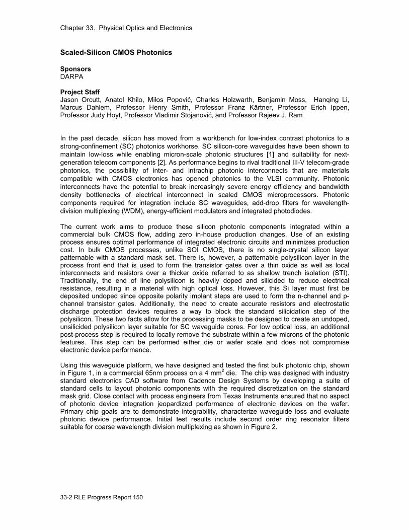
Scaled-Silicon CMOS Photonics Sponsors DARPA Project Staff Jason Orcutt, Anatol Khilo, Milos Popović, Charles Holzwarth, Benjamin Moss, Hanqing Li, Marcus Dahlem, Professor Henry Smith, Professor Franz Kärtner, Professor Erich Ippen, Professor Judy Hoyt, Professor Vladimir Stojanović, and Professor Rajeev J. Ram In the past decade, silicon has moved from a workbench for low-index contrast photonics to a strong-confinement (SC) photonics workhorse. SC silicon-core waveguides have been shown to maintain low-loss while enabling micron-scale photonic structures [1] and suitability for next-generation telecom components [2]. As performance begins to rival traditional III-V telecom-grade photonics, the possibility of inter- and intrachip photonic interconnects that are materials compatible with CMOS electronics has opened photonics to the VLSI community. Photonic interconnects have the potential to break increasingly severe energy efficiency and bandwidth density bottlenecks of electrical interconnect in scaled CMOS microprocessors. Photonic components required for integration include SC waveguides, add-drop filters for wavelength-division multiplexing (WDM), energy-efficient modulators and integrated photodiodes. The current work aims to produce these silicon photonic components integrated within a commercial bulk CMOS flow, adding zero in-house production changes. Use of an existing process ensures optimal performance of integrated electronic circuits and minimizes production cost. In bulk CMOS processes, unlike SOI CMOS, there is no single-crystal silicon layer patternable with a standard mask set. There is, however, a patternable polysilicon layer in the process front end that is used to form the transistor gates over a thin oxide as well as local interconnects and resistors over a thicker oxide referred to as shallow trench isolation (STI). Traditionally, the end of line polysilicon is heavily doped and silicided to reduce electrical resistance, resulting in a material with high optical loss. However, this Si layer must first be deposited undoped since opposite polarity implant steps are used to form the n-channel and p-channel transistor gates. Additionally, the need to create accurate resistors and electrostatic discharge protection devices requires a way to block the standard silicidation step of the polysilicon. These two facts allow for the processing masks to be designed to create an undoped, unsilicided polysilicon layer suitable for SC waveguide cores. For low optical loss, an additional post-process step is required to locally remove the substrate within a few microns of the photonic features. This step can be performed either die or wafer scale and does not compromise electronic device performance. Using this waveguide platform, we have designed and tested the first bulk photonic chip, shown in Figure 1, in a commercial 65nm process on a 4 mm2 die. The chip was designed with industry standard electronics CAD software from Cadence Design Systems by developing a suite of standard cells to layout photonic components with the required discretization on the standard mask grid. Close contact with process engineers from Texas Instruments ensured that no aspect of photonic device integration jeopardized performance of electronic devices on the wafer. Primary chip goals are to demonstrate integrability, characterize waveguide loss and evaluate photonic device performance. Initial test results include second order ring resonator filters suitable for coarse wavelength division multiplexing as shown in Figure 2.
Chapter 33. Physical Optics and Electronics
33-3
1260 1265 1270
-80
-70
-60
-50Through Port Transfer Function
Wavelength (nm)
Transmission (dB
)
1260 1265 1270
-90
-80
-70
-60
Drop Port Transfer Function
Wavelength (nm)
Transmission (dB
)
~30 dBextinction
~130 GHz3 dB width
(a)
(b)
Figure 1: Bulk 65 nm photonic test chip die photo. 2x2 mm2 die contains 116 devices and over 21 cm of waveguide.
Figure 2: Measured second order microring resonator filter through (a) and drop (b) port transmission functions. Waveguide coupling reflections result in the 1.5 nm period amplitude modulation.
[1] F. Xia, et al., “Ultracompact optical buffers of a silicon chip,” in Nat. Phot. 1, pp. 65-71,
(2007). [2] M.A. Popović, T. Barwicz, et al., “Strong-confinement microring resonator photonic circuits,”
in Proc. 20th An. Meet. IEEE Lasers and Electro-Optics Soc. (LEOS), Lake Buena Vista, Florida, Oct 2007, paper TuCC3.
Chapter 33. Physical Optics and Electronics
33-4 RLE Progress Report 150
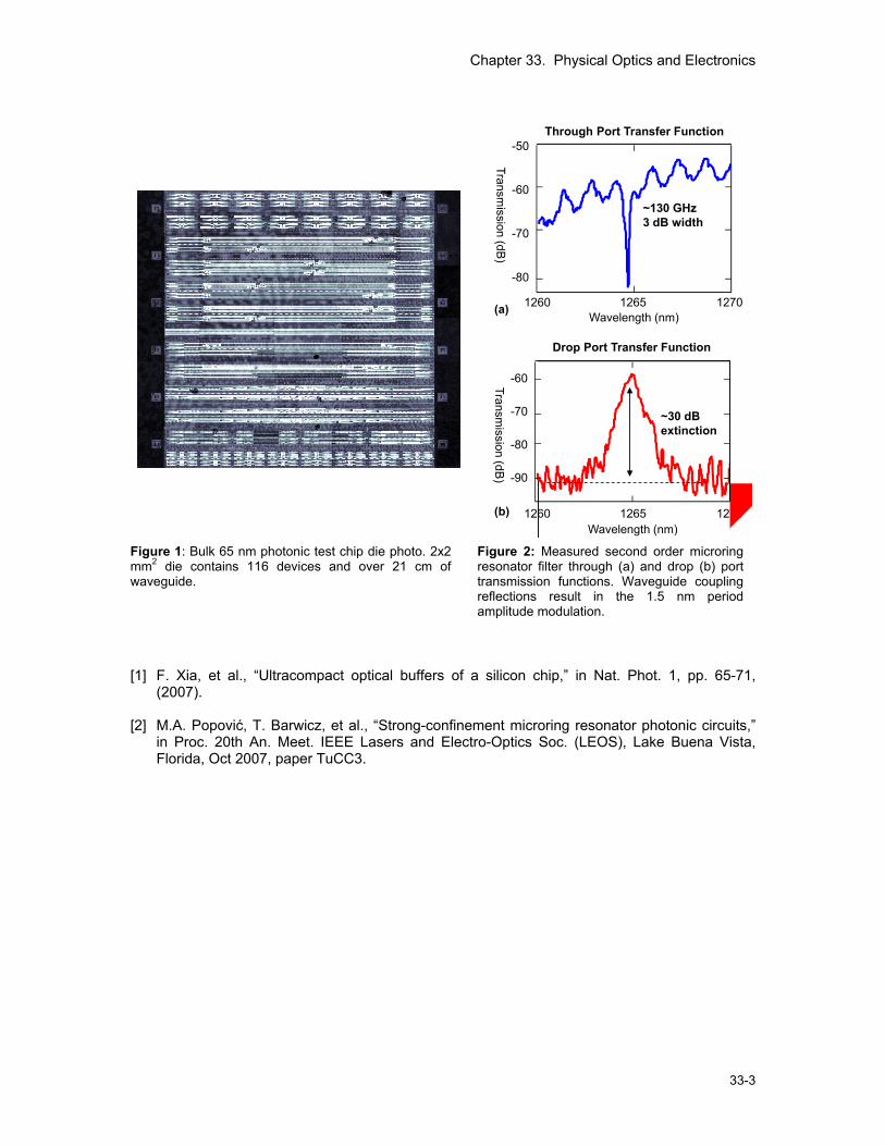
Actively Stabilized Microring Resonators Sponsors DARPA Project Staff Reja Amatya, Professor Rajeev J. Ram Charles Holzwarth, Professor Henry I Smith Microring resonators can be used as passband filters for wavelength-division demultiplexing in electronic-photonic integrated circuits for applications such as analog-to-digital converters. For high quality signal transmission, the resonant frequency of the filter has to be held at a certain value to allow minimum timing errors in the sampling of the signal. Thermal tuning is used to compensate for any fabrication errors or environmental temperature fluctuations that might lead to a shift in the resonant frequency. With an optimized heater design (Fig. 1) and a temperature controller feedback circuit, we demonstrate efficient thermal tuning with low power (80μW/GHz) for these ring resonators. Due to size constraints for microring resonators (radius ~ 10 μm), a single resistive element is used both as a heater and as a temperature sensor. The feedback circuit utilizing a proportional-integral-derivative (PID) controller maintains the overall balance between the voltages of the heater and the set resistor such that the error in the voltage difference measured by an instrumentation amplifier is minimized. To show the thermal stability of the system and the resolution of the temperature controller circuit, an experiment was conducted, where an external temperature perturbation is introduced by shining a white light source on the sample. When the light is on, a temperature variation of 1 K is introduced to the filter chip. With the closed-loop feedback, the temperature variation is reduced to an average fluctuation of 80 mK which is equivalent to the frequency variation of 280 MHz (Fig. 2). The speed of the feedback circuit to compensate for the temperature perturbation is in the order of a few tens of milliseconds.
Figure 2: Thermal control achieved within 80 mK
of the absolute value for the second-order ring resonator using feedback control loop.
Figure 1: SEM picture of the microring heater on top of the filter.
Chapter 33. Physical Optics and Electronics
33-5
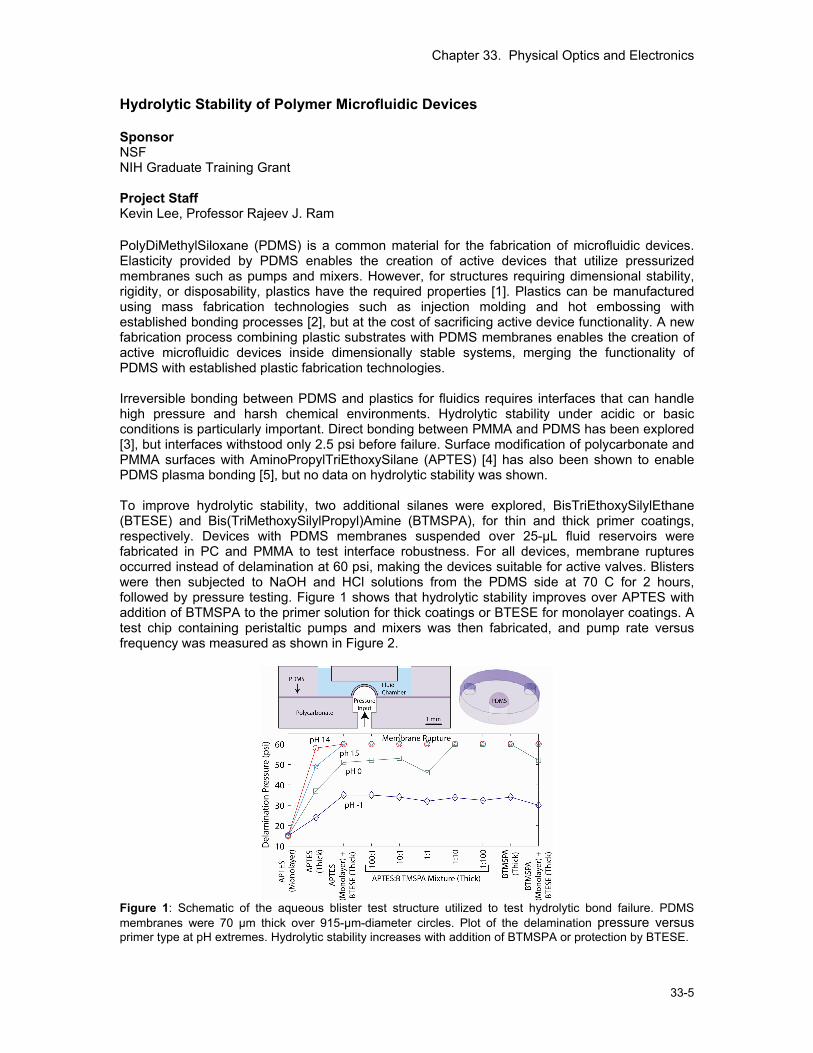
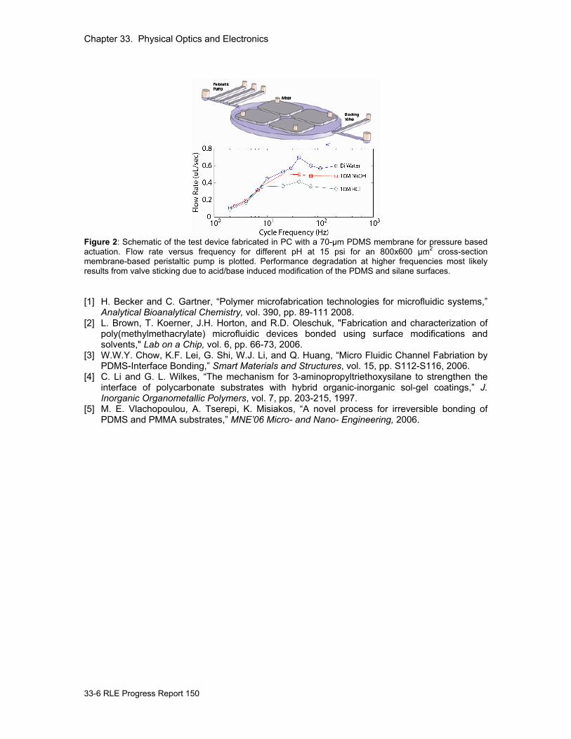
Hydrolytic Stability of Polymer Microfluidic Devices Sponsor NSF NIH Graduate Training Grant Project Staff Kevin Lee, Professor Rajeev J. Ram PolyDiMethylSiloxane (PDMS) is a common material for the fabrication of microfluidic devices. Elasticity provided by PDMS enables the creation of active devices that utilize pressurized membranes such as pumps and mixers. However, for structures requiring dimensional stability, rigidity, or disposability, plastics have the required properties [1]. Plastics can be manufactured using mass fabrication technologies such as injection molding and hot embossing with established bonding processes [2], but at the cost of sacrificing active device functionality. A new fabrication process combining plastic substrates with PDMS membranes enables the creation of active microfluidic devices inside dimensionally stable systems, merging the functionality of PDMS with established plastic fabrication technologies. Irreversible bonding between PDMS and plastics for fluidics requires interfaces that can handle high pressure and harsh chemical environments. Hydrolytic stability under acidic or basic conditions is particularly important. Direct bonding between PMMA and PDMS has been explored [3], but interfaces withstood only 2.5 psi before failure. Surface modification of polycarbonate and PMMA surfaces with AminoPropylTriEthoxySilane (APTES) [4] has also been shown to enable PDMS plasma bonding [5], but no data on hydrolytic stability was shown. To improve hydrolytic stability, two additional silanes were explored, BisTriEthoxySilylEthane (BTESE) and Bis(TriMethoxySilylPropyl)Amine (BTMSPA), for thin and thick primer coatings, respectively. Devices with PDMS membranes suspended over 25-µL fluid reservoirs were fabricated in PC and PMMA to test interface robustness. For all devices, membrane ruptures occurred instead of delamination at 60 psi, making the devices suitable for active valves. Blisters were then subjected to NaOH and HCl solutions from the PDMS side at 70 C for 2 hours, followed by pressure testing. Figure 1 shows that hydrolytic stability improves over APTES with addition of BTMSPA to the primer solution for thick coatings or BTESE for monolayer coatings. A test chip containing peristaltic pumps and mixers was then fabricated, and pump rate versus frequency was measured as shown in Figure 2.
Figure 1: Schematic of the aqueous blister test structure utilized to test hydrolytic bond failure. PDMS membranes were 70 µm thick over 915-µm-diameter circles. Plot of the delamination pressure versus primer type at pH extremes. Hydrolytic stability increases with addition of BTMSPA or protection by BTESE.
Chapter 33. Physical Optics and Electronics
33-6 RLE Progress Report 150
Figure 2: Schematic of the test device fabricated in PC with a 70-µm PDMS membrane for pressure based actuation. Flow rate versus frequency for different pH at 15 psi for an 800x600 µm2 cross-section membrane-based peristaltic pump is plotted. Performance degradation at higher frequencies most likely results from valve sticking due to acid/base induced modification of the PDMS and silane surfaces. [1] H. Becker and C. Gartner, “Polymer microfabrication technologies for microfluidic systems,”
Analytical Bioanalytical Chemistry, vol. 390, pp. 89-111 2008. [2] L. Brown, T. Koerner, J.H. Horton, and R.D. Oleschuk, "Fabrication and characterization of
poly(methylmethacrylate) microfluidic devices bonded using surface modifications and solvents," Lab on a Chip, vol. 6, pp. 66-73, 2006.
[3] W.W.Y. Chow, K.F. Lei, G. Shi, W.J. Li, and Q. Huang, “Micro Fluidic Channel Fabriation by PDMS-Interface Bonding,” Smart Materials and Structures, vol. 15, pp. S112-S116, 2006.
[4] C. Li and G. L. Wilkes, “The mechanism for 3-aminopropyltriethoxysilane to strengthen the interface of polycarbonate substrates with hybrid organic-inorganic sol-gel coatings,” J. Inorganic Organometallic Polymers, vol. 7, pp. 203-215, 1997.
[5] M. E. Vlachopoulou, A. Tserepi, K. Misiakos, “A novel process for irreversible bonding of PDMS and PMMA substrates,” MNE’06 Micro- and Nano- Engineering, 2006.
Chapter 33. Physical Optics and Electronics
33-7
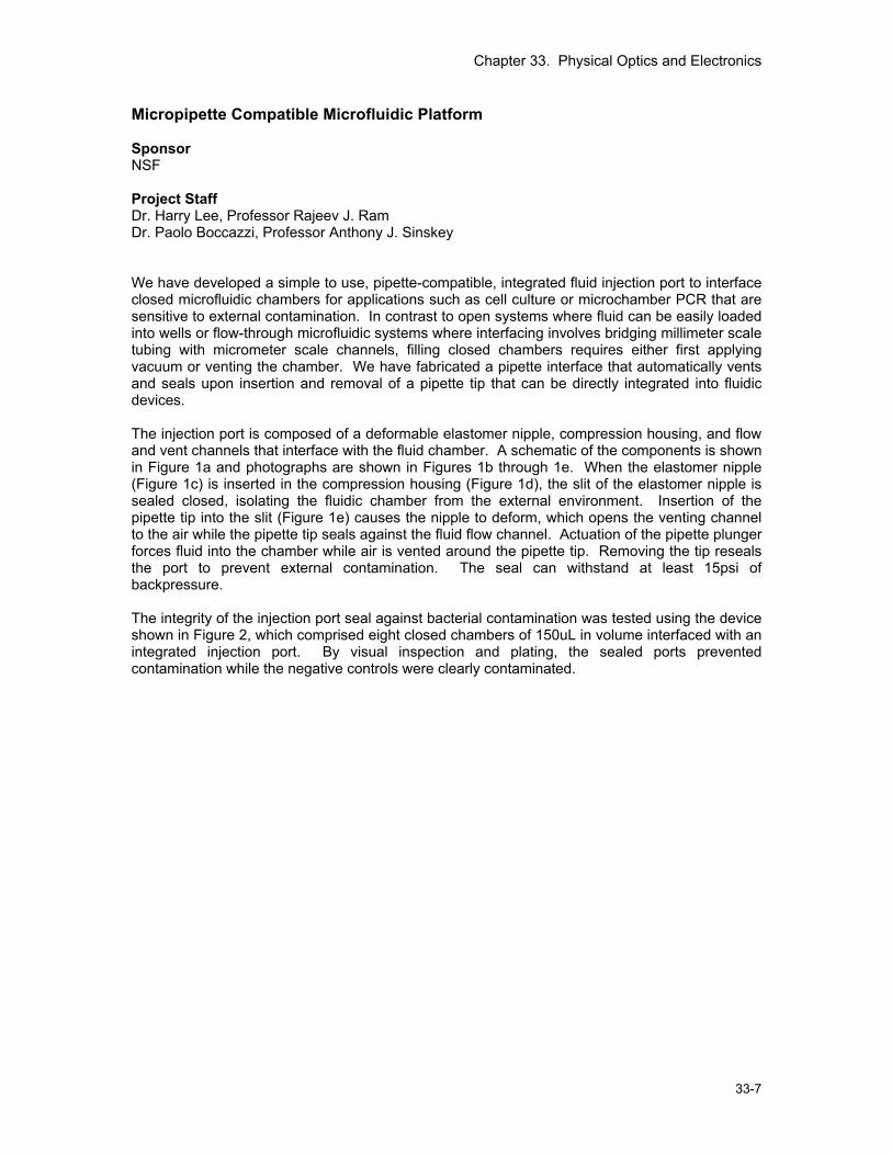
Micropipette Compatible Microfluidic Platform Sponsor NSF Project Staff Dr. Harry Lee, Professor Rajeev J. Ram Dr. Paolo Boccazzi, Professor Anthony J. Sinskey We have developed a simple to use, pipette-compatible, integrated fluid injection port to interface closed microfluidic chambers for applications such as cell culture or microchamber PCR that are sensitive to external contamination. In contrast to open systems where fluid can be easily loaded into wells or flow-through microfluidic systems where interfacing involves bridging millimeter scale tubing with micrometer scale channels, filling closed chambers requires either first applying vacuum or venting the chamber. We have fabricated a pipette interface that automatically vents and seals upon insertion and removal of a pipette tip that can be directly integrated into fluidic devices. The injection port is composed of a deformable elastomer nipple, compression housing, and flow and vent channels that interface with the fluid chamber. A schematic of the components is shown in Figure 1a and photographs are shown in Figures 1b through 1e. When the elastomer nipple (Figure 1c) is inserted in the compression housing (Figure 1d), the slit of the elastomer nipple is sealed closed, isolating the fluidic chamber from the external environment. Insertion of the pipette tip into the slit (Figure 1e) causes the nipple to deform, which opens the venting channel to the air while the pipette tip seals against the fluid flow channel. Actuation of the pipette plunger forces fluid into the chamber while air is vented around the pipette tip. Removing the tip reseals the port to prevent external contamination. The seal can withstand at least 15psi of backpressure. The integrity of the injection port seal against bacterial contamination was tested using the device shown in Figure 2, which comprised eight closed chambers of 150uL in volume interfaced with an integrated injection port. By visual inspection and plating, the sealed ports prevented contamination while the negative controls were clearly contaminated.
Chapter 33. Physical Optics and Electronics
33-8 RLE Progress Report 150
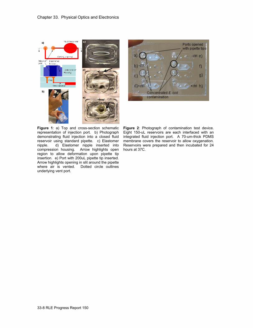
Figure 1: a) Top and cross-section schematic representation of injection port. b) Photograph demonstrating fluid injection into a closed fluid reservoir using standard pipette. c) Elastomer nipple. d) Elastomer nipple inserted into compression housing. Arrow highlights open region to allow deformation upon pipette tip insertion. e) Port with 200uL pipette tip inserted. Arrow highlights opening in slit around the pipette where air is vented. Dotted circle outlines underlying vent port.
Figure 2: Photograph of contamination test device. Eight 150-uL reservoirs are each interfaced with an integrated fluid injection port. A 70-um-thick PDMS membrane covers the reservoir to allow oxygenation. Reservoirs were prepared and then incubated for 24 hours at 37C.
Chapter 33. Physical Optics and Electronics
33-9
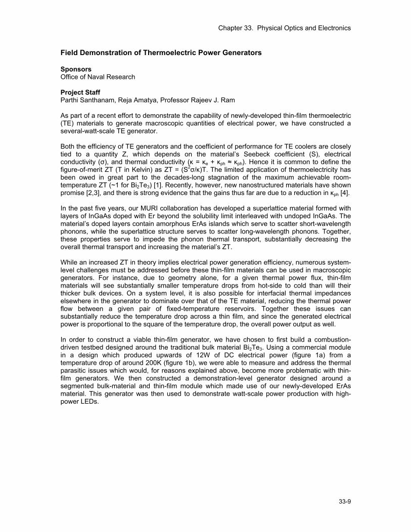
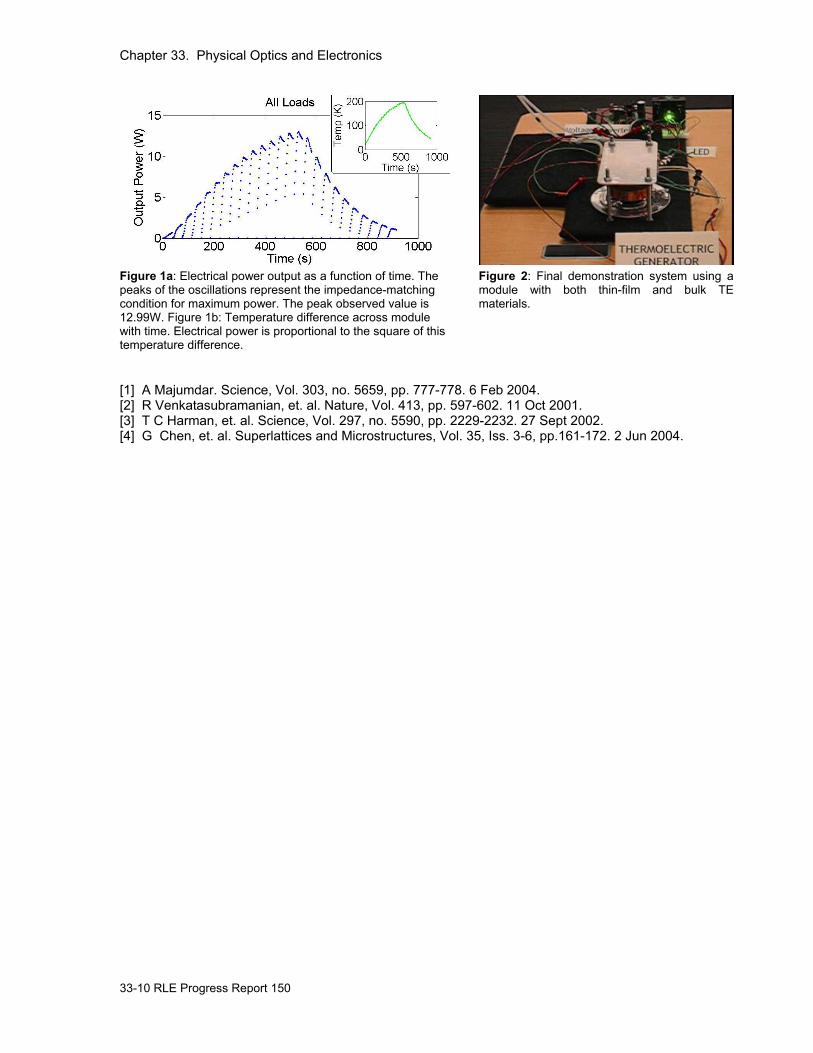
Field Demonstration of Thermoelectric Power Generators Sponsors Office of Naval Research Project Staff Parthi Santhanam, Reja Amatya, Professor Rajeev J. Ram As part of a recent effort to demonstrate the capability of newly-developed thin-film thermoelectric (TE) materials to generate macroscopic quantities of electrical power, we have constructed a several-watt-scale TE generator. Both the efficiency of TE generators and the coefficient of performance for TE coolers are closely tied to a quantity Z, which depends on the material’s Seebeck coefficient (S), electrical conductivity (σ), and thermal conductivity (κ = κe + κph ≈ κph). Hence it is common to define the figure-of-merit ZT (T in Kelvin) as ZT = (S2σ/κ)T. The limited application of thermoelectricity has been owed in great part to the decades-long stagnation of the maximum achievable room-temperature ZT (~1 for Bi2Te3) [1]. Recently, however, new nanostructured materials have shown promise [2,3], and there is strong evidence that the gains thus far are due to a reduction in κph [4]. In the past five years, our MURI collaboration has developed a superlattice material formed with layers of InGaAs doped with Er beyond the solubility limit interleaved with undoped InGaAs. The material’s doped layers contain amorphous ErAs islands which serve to scatter short-wavelength phonons, while the superlattice structure serves to scatter long-wavelength phonons. Together, these properties serve to impede the phonon thermal transport, substantially decreasing the overall thermal transport and increasing the material’s ZT. While an increased ZT in theory implies electrical power generation efficiency, numerous system-level challenges must be addressed before these thin-film materials can be used in macroscopic generators. For instance, due to geometry alone, for a given thermal power flux, thin-film materials will see substantially smaller temperature drops from hot-side to cold than will their thicker bulk devices. On a system level, it is also possible for interfacial thermal impedances elsewhere in the generator to dominate over that of the TE material, reducing the thermal power flow between a given pair of fixed-temperature reservoirs. Together these issues can substantially reduce the temperature drop across a thin film, and since the generated electrical power is proportional to the square of the temperature drop, the overall power output as well. In order to construct a viable thin-film generator, we have chosen to first build a combustion-driven testbed designed around the traditional bulk material Bi2Te3. Using a commercial module in a design which produced upwards of 12W of DC electrical power (figure 1a) from a temperature drop of around 200K (figure 1b), we were able to measure and address the thermal parasitic issues which would, for reasons explained above, become more problematic with thin-film generators. We then constructed a demonstration-level generator designed around a segmented bulk-material and thin-film module which made use of our newly-developed ErAs material. This generator was then used to demonstrate watt-scale power production with high-power LEDs.
Chapter 33. Physical Optics and Electronics
33-10 RLE Progress Report 150
Figure 1a: Electrical power output as a function of time. The peaks of the oscillations represent the impedance-matching condition for maximum power. The peak observed value is 12.99W. Figure 1b: Temperature difference across module with time. Electrical power is proportional to the square of this temperature difference.
Figure 2: Final demonstration system using a module with both thin-film and bulk TE materials.
[1] A Majumdar. Science, Vol. 303, no. 5659, pp. 777-778. 6 Feb 2004. [2] R Venkatasubramanian, et. al. Nature, Vol. 413, pp. 597-602. 11 Oct 2001. [3] T C Harman, et. al. Science, Vol. 297, no. 5590, pp. 2229-2232. 27 Sept 2002. [4] G Chen, et. al. Superlattices and Microstructures, Vol. 35, Iss. 3-6, pp.161-172. 2 Jun 2004.