Embed Size (px)
Citation preview

8OPTICAL PROPERTIES
8.1 OPTICAL DISPERSION RELATIONS
In! _xGaxAsyPi -y/lnP heterostructures become increasingly interesting aslight sources and detectors for optical fiber communication systems in the1.4-1.7-/xm wavelength region. Knowledge of optical properties is veryimportant in the design and analysis of such optoelectronic devices.
The complex dielectric function
e(co) = e,(co) + ie2((o) (8.1)
is known to describe the optical properties of the medium at all photonenergies E = hu. Real (e^ and imaginary (e2) parts of the dielectric func-tion are connected by the well-known Kramers-Kronig (KK) relations:1
(CO
t \ 2 f °° 6 l(^ f>€2(CJ) = -~ \ 7-7^
7T JO (CO ) —
The complex refractive index n*(co) = «(co) + ik(u>) is now given by
n* = n(co) + i*((o) = [e,(w) -f i€2(w)]1/2 (8.3)
135
Physical Properties of III-VSemiconductor Compounds. Sadao AdachiCopyright © 1992 by John Wiley & Sons, Inc. ISBN: 0-471-57329-9

136 OPTICAL PROPERTIES
where AZ(CO) is the real refractive index and k(u) is the extinction coefficient,also called the attenuation index. The constants n(co) and k(u) are real andpositive numbers and can be determined by optical measurements. FromEqs. (8.1) and (8.3), it follows that
€| = n2 - k2, e2 = 2nk (8.4)
and also that
„,„) = (8.5)
The absorption coefficient a(o;) depends not only on e2(co) but also onboth parts of the dielectric function
a(w) = ̂ *(«) (8.7)A
where X is the wavelength of light in the vacuum.The normal-incidence reflectivity R is
R =n* - 1
+ 1
2(n ~ I)2 + k2
(n + I)2 + k2 (8.8)
8.2 THE RESTSTRAHLEN REGION
The reststrahlen region is the region where the radiation field interacts withthe fundamental lattice vibrations. Two effects resulted: (1) absorption oremission of the electromagnetic wave due to the creation or annihilation oflattice vibrations and (2) scattering of the electromagnetic wave by the lat-tice vibrational modes. Optical absorption due to lattice vibrations appearsas absorption bands in the infrared region (with wavelength range of a fewtens of micrometers) attributed either to a first- or second-order electronicdipole moment or to anharmonic terms in the potential energy. In polarcrystals, as in InP, the first-order dipole moment gives rise to a very strongabsorption band associated with optical modes having an of essentially zerok vector (i.e., long-wavelength optical phonons). A useful description ofthe theoretical and practical aspects of this subject is given by Balkanski.2
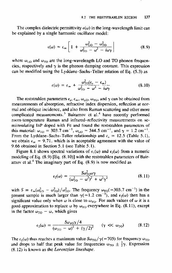
8.2 THE RESTSTRAHLEN REGION 137
The complex dielectric permittivity e(co) in the long-wavelength limit canbe explained by a single harmonic oscillator model:
6 ( a O ~ e l + (8.9)L COTO - coz - ivy]
where COLO and COTO are the long-wavelength LO and TO phonon frequen-cies, respectively and y is the phonon damping constant. This expressioncan be modified using the Lyddane-Sachs-Teller relation of Eq. (5.3) as
x 2 2 °°. (8.10)coTO — co — lory
The reststrahlen parameters es, e^,, COLO, COTO, and y can be obtained frommeasurements of absorption, refractive index dispersion, reflection at nor-mal and oblique incidence, and also from Raman scattering and other morecomplicated measurements.3 Bairamov et al.4 have recently performedroom-temperature Raman and infrared-reflectivity measurements on se-miinsulating InP doped with Fe and found the reststrahlen parameters ofthis material: COTO = 303.7 cm"1, COLO = 344.5 cm"1, and y = 1.2 cm"1.From the Lyddane-Sachs-Teller relationship and es = 12.5 (Table 5.1),we obtain e^ = 9.71, which is in acceptable agreement with the value of9.66 obtained in Section 5.1 (see Table 5.1).
Figure 8.1 shows spectral variations of e^co) and e2(to) from a numericmodeling of Eq. (8.9) [Eq. (8.10)] with the reststrahlen parameters of Bair-amov et al.4 The imaginary part of Eq. (8.9) is now modified as
&OTQCQ7 (8-n)
with S = €00(00^0 — ̂ TO)/^TO- The frequency coTO(=303.7 cm"1) in thepresent sample is much larger than 7(=1,2 cm"1), and e2(co) then has asignificant value only when co is close to COTO. For such values of co it is agood approximation to replace co by COTO everywhere in Eq. (8.11), exceptin the factor COTO - co, which gives
WTO)< < n*(COTO - co) 4- (7/2)
The e2(co) thus reaches a maximum value ScoTO/7( = 705) for frequency COTO
and drops to half that peak value for frequencies COTO ± ^7. Expression(8.12) is known as the Lorentzian lineshape.

138 OPTICAL PROPERTIES
800i
600
400
200
-200
-400260 280 300 320 340
FREQUENCY ( cm-1 )
Figure 8.1 Spectral variation of e(w) obtained from a numeric modeling of Eq. (8.9) [Eq.(8.10)] with the reststrahlen parameters of semiinsulating InP determined at room temper-ature by Bairamov et al.4
The corresponding variations of n(co) and fc(co) obtained from Eqs. (8.5)and (8.6) are shown in Fig. 8.2. The absorption coefficient a and normal-incidence reflectivity R as calculated from Eqs. (8.7) and (8.8) are alsoshown in Figs. 8.3 and 8.4, respectively. Both n and k(a) dispersion curvesshow a strong peak at the resonance frequency co = COTO. The reflectivityR at co close to COLO is nearly zero.
The optical properties at the reststrahlen region in semiinsulating crystalsare adequately well interpreted by the above-mentioned single harmonicoscillator model. If free carriers are present in the medium, we must takeinto account plasma contributions to the dielectric permittivity. When thefrequency of free-carrier plasma excitations (plasmons) is close to the fre-quency of the LO phonons (COLO), the two excitations interact via their mac-roscopic electric fields. The dielectric permittivity in such case is given by
e(co) = 1 +COTO — CO co(co + iT)
(8.13)

8.2 THE RESTSTRAHLEN REGION 139
25
20-
15
10
InP
220 260 300 340FREQUENCY ( cm'1 )
380
Figure 8.2 Numerically calculated spectral dependence of the real refractive index (n) andthe extinction coefficient (k) at the reststrahlen region of InP using the same set of rest-strahlen parameters as in Fig. 8.1.
where
ne 1/2
(8.14)
is the plasma frequency, F is the plasmon damping constant, and n and m*are, respectively, the concentration and effective mass of the free carriers.Expression (8.13) has been used as the basis for sorting out plasmon-phonon effects in a number of investigations (see review by Blakemore3).Kukharskii,5 however, showed that this expression oversimplifies the cou-pling of plasmons and phonons and can lead, principally, to errors in de-ducing the damping constants y and F. In Kukharskii's model, e(o>) is givenby
(co2 - co2_)(qj2 /F+co - co2+)(8.15)

140 OPTICAL PROPERTIES
10
InP
220 260 300 340 380
FREQUENCY ( cm'1 )
Figure 8.3 Numerically calculated spectral dependence of the absorption coefficient a atthe reststrahlen region of InP using the same set of reststrahlen parameters as in Fig. 8.1.
where
co2 = - 4<o24o]1/2} (8.16)
In his model two additional parameters are the damping constants F+ ofthe coupled plasmon-phonon modes. The plasmon and single-oscillatormodels are related to each other through the equation
cd_|_Gj_ == ojpCJjQ (8.17)
Bairamov et al.4 have also measured room-temperature infrared-reflec-tivity spectra of n-type InP doped with Sn and S in the concentration rangefrom 6.8 x 10¹⁷ to 1 x 1019 cm'1. We reproduce their results in Fig. 8.5.The reflectance minimum at about 300 cm"1 is due to the LO phonon. Theposition of the second minimum, called the plasma minimum, depends on

8.2 THE RESTSTRAHLEN REGION 141
1.0
0.8
0.6
0.4
0.2
InP
220 240 260 280 300 320 340 360 380
FREQUENCY ( cm"1 )
Figure 8.4 Numerically calculated spectral dependence of the normal-incidence reflectiv-ity R at the reststrahlen region of InP using the same set of reststrahlen parameters as inFig. 8.1.
R 1
100 300 500 700 900 1100 1300 1500
FREQUENCY (cm'1 )
Figure 8.5 Room-temperature infrared reflectivity data for n-type InP. The carrier con-centrations are 8.8 x 1018 cm""3 (#1), 7.1 X 1018 cm~3 (#2), 2.3 x 1018 cm~3 (#3), and4.9 x 1017 cm~3 (#4). The minimum at about 300 cm"1 is due to the LO phonons. Theposition of the second minimum, called the plasma minimum, depends on the electron con-centration. (From Bairamov et al.4)

142 OPTICAL PROPERTIES
the electron concentration. The plasma resonance minimum is very closeto the TO-phonon line in the spectrum of the relatively lightly doped sam-ple (#1 in Fig. 8.5). When the carrier concentration is larger (#2-#4), theplasma minimum is shifted toward higher photon energies as seen in Fig.8.5. The carrier concentrations are obtained from Eq. (8.14). Because InPhas a nonparabolic conduction band, the effective mass m*( = ml) in Eq.(8.14) depends on the carrier concentration (see Chapter 6). This non-parabolic-band correction is given by Eq. (6.10) and has been taken intoconsideration in the calculations.
Reflection spectra of bulk alloy samples usually consist of lattice bands,the number of which is equal to the number of different cells. For example,the reflectance spectra of In^/ja^As^F^ consist of four lattice bands(i.e., four-mode behavior; see Section 3.3). The dielectric permittivity insuch materials can be successfully explained by the following multioscil-lator model:
, . . V ,Q , 0 V
€(0)) = €00 + Zj — - 2 - : --- , , -Tiv (8-18)— co — tujj co(co + 1 1 )
where 57[ = e^co^o, - «TOy)/wTo/l *s the oscillator strength, coTq/ is the TOphonon frequency, and 7, the damping constant of they th lattice oscillator.
As mentioned in Section 3.3, many authors have performed optical stud-ies in the reststrahlen region of the In, _xGaxAsyPi _y quaternary using theRaman and/or far-infrared-reflectivity techniques. However, such workswere focused mainly on the phonon-mode determination (the four- or three-mode behavior). Straightforward information about the optical constants inthe reststrahlen region of this alloy is, thus, very scant.6'8
Pickering8 determined the four-mode lattice vibrational behavior inIn, _^cGaA.As>,PI _y lattice-matched to InP over most of the compositionrange using a far-infrared-reflectivity technique. Representative examplesof the spectra he obtained near the middle of the composition range (y =0.35 and 0.50) are shown in Fig. 8.6. The four lattice bands and the plasmaedge can be clearly recognized in the spectra. The solid lines are the resultsof fits to Eq. (8.18) with four oscillators (j = 1-4). The fits are seen to befairly good except in the higher-frequency region, where the penetrationdepth is high and effects of any nonabrupt junctions will be most notice-able. The composition dependence of the oscillator strengths (S, values)was also found to be proportional to the pair concentration [i.e., (1 - ;c)(1 - y) for the InP-mode oscillator, (1 - x)y for the InAs-mode one, xyfor the GaAs-mode one, and x(l — y) for the GaP-mode one] for a randomalloy.8

8.3 THE INTERBAND TRANSITION REGION 143
0.6
OA
0.2
OA
0.2
y=0.35
Rasma InAs GaAs InP GaP '
t t t t
1 T
100 200 300 400FREQUENCY (cm"1 )
Figure 8.6 Room-temperature infrared reflectivity data for In, .^Ga^As^Pi _>f quaternary(y - 0.35 and 0.50). The solid lines represent the results of fits to Eq. (8.18) with fouroscillators. (From Pickering.8)
8.3 THE INTERBAND TRANSITION REGION
8.3.1 Mode! Dielectric Function
Let us first present various approximations9 of the dielectric constants inthe interband transition region of semiconductors. Figures 8.7«-/show theapproximations used in the case of tetragonal semiconductors to describethe refractive-index dispersion below the fundamental absorption edge[rc(co) — €i(o))°'5]. The dashed curves are the spectral dependence e2(co)typical of the diamond- and zinc-blende-type structures. The continuouscurves represent the various model representations of e2(o>) used in Refs.10-15.
The nature of the spectrum of e2(co) in the fundamental absorption regionof direct-gap semiconductors is well characterized by a square-root depen-dence, €2(w) oc (#o> - £0)
05 (Fig. 8.7010'11). Wemple and DiDomenicohave proposed a semiempirical single-effective-oscillator model to analyzerefractive index dispersion in more than 100 widely different solids andliquids (Fig. 8.7b12). Their model requires two parameters, Ep and £d,where the imaginary part of the dielectric constant e2 of the material wasassumed to be a delta function at energy £p and the strength of the effective

144 OPTICAL PROPERTIES
(a) (b) (c)
u E, Eo Eo E,EPEO
(d) (e)
E_ E E'
i1:1:':!:':'̂SssSr'
( f)
E E E'ci p 0 Ei E'•hu ( eV )
Figure 8.7 Imaginary part of the dielectric constant e(co) (dashed lines) in the interbandtransition region and its model representations (solid lines) used in Refs. 10 and 11 (a), 12(b), 13 (c), 14 (d), and 15 (e, /) for semiconductors with diamond and zinc-blend struc-tures.
oscillator was defined to be 7r£'d/2. The KK transformation of this functiongives
(8.19)
where E = ftco. On the other hand, Stern considered a two-oscillator modelthat assumes effective oscillators at energies E} and E2 (Fig. 8.7c13). Mat-ters are, however, complicated by the lack of agreement of the data withthe Wemple-DiDomenico or Stern model at the direct-band edge, which isthe energy range of most interest for semiconductor optoelectronic devices.Afromowitz has therefore proposed a modified single-effective-oscillatormodel (Fig. 8.7rf14), which takes into account the lowest-direct-gap con-tribution, and applied it to ! .^As, i _y, and In! ter-naries. In the Afromowitz model the contribution of the lowest-direct gapEQ to e2(co) was assumed to have the form of e2(co) oc (//a))4. His assumede2(o>) agrees closely with the actual spectrum in the region below E{ (seeFig. 8.7d) but is fully empirically derived and therefore nonphysical. Pikh-

8.3 THE INTERS AND TRANSITION REGION 145
tin and coworkers' model representations of e2(co) also allow for the elec-tronic density of states, which is assumed to be uniformly distributed in theinterval between hu = EQ - E} (Fig. 8.7e15), hu = £0 "~ E\ and #co =£, - E2 (Fig. 8.7/15). It seems that all these approximations oversimplifythe actual e2(co) spectra.
Let us now present a new model of the dielectric functions e,(o)) ande2(co), which covers the optical response of semiconductors over a widerange of photon energies. 16~24 The model is based on the KK transformation[Eq. (8.2)] and is strongly connected with the electronic energy-band struc-ture of the medium (Chapter 6). This model predicts distinct structures atenergies of E0, ^o + A0, £",, /?, + A,, and EQ critical points (CP). Theindirect-band-gap transitions also play an important part in the spectral de-pendence of both e, and e2.
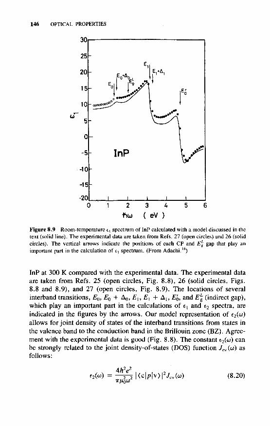
In Figs. 8.8 and 8.9 we show our calculated e2(w) and e,(o>) spectra of
100
10
b)
0.1
0.01
InP
2 3 4 5 6
( eV )
8 9
Figure 8.8 Room-temperature e2 spectrum of InP calculated with a model discussed in thetext (solid line). The experimental data are taken from Refs. 25 (open circles) and 26 (solidcircles). The vertical arrows indicate the positions of each CP (critical point) and Eg gapthat play an important part in the calculation of e2 spectrum. (From Adachi.16)
146 OPTICAL PROPERTIES
30
U)
Figure 8.9 Room-temperature e{ spectrum of InP calculated with a model discussed in thetext (solid line). The experimental data are taken from Refs. 27 (open circles) and 26 (solidcircles). The vertical arrows indicate the positions of each CP and EL
% gap that play animportant part in the calculation of e, spectrum. (From Adachi.16)
InP at 300 K compared with the experimental data. The experimental dataare taken from Refs. 25 (open circles, Fig. 8.8), 26 (solid circles, Figs.8.8 and 8.9), and 27 (open circles, Fig. 8.9). The locations of severalinterband transitions, EQ, E0 + A0, /?,, £, + A l 9 £Q, and Eg (indirect gap),which play an important part in the calculations of e{ and e2 spectra, areindicated in the figures by the arrows. Our model representation of £2(^)allows for joint density of states of the interband transitions from states inthe valence band to the conduction band in the Brillouin zone (BZ). Agree-ment with the experimental data is good (Fig. 8.8). The constant e2(co) canbe strongly related to the joint density-of-states (DOS) function Jcv (co) asfollows:
2 2
(8.20)

8.3 THE INTERS AND TRANSITION REGION 147
where ^0 is the combined DOS mass and <c|/?|v> is the momentum matrixelement for v (valence) -> c (conduction) transitions. Thus /cv(co) of par-amount importance for the explanation of optical spectra, and its analyticbehavior at various types of CP in the BZ can be calculated.28 In the fol-lowing we summarize the model dielectric functions for CP of each energygap (£"0, E0 + A0, E}9 E{ - H A , , EJ, and indirect-band gap), in HI-V, zinc-blende-type materials. Combining all these contributions, we can obtainthe spectral dependence of e(o>) of the materials in the entire range of pho-ton energies.16'24
(a) EQ and EQ + A0 Transitions The EQ and £"0 + AO transitions are ofthe three-dimensional (3D) Af0 CPs. Assuming that the bands are parabolicand using the KK relation, we obtain the contribution of these gaps to e(w):
/(xso)} (8.21)
with
A = \(\^'5P2 (8.22)
/(Xo) = Xo"2[2 - (1 + Xo)0'5 - (1 + Xo)a5] (8.23a)
/(Xso) = Xs"o2[2 - (1 + Xso)°5 - 0 + xso)°5] (8.23b)
hu + iTXo = — ~ - (8.24a)
X. -
where P2 is the squared momentum matrix element and F is the broadeningconstant of the EG/(E0 + A0) transitions. Here, for simplicity, the reducedmass JLCO for the three valence bands is assumed to be equal.
In Fig. 8.10 we show our calculated e(co) spectra of Eq. (8.21) [e2(co) =Im e(co); ^(oj) = Re e(o>)]. The numeric parameters used in the calculationscorrespond to those for InP and are as follows: /SQ = 1-35 eV, EQ 4- A0 =1 .47 eV, A = 5.4 eV1 5, and F = 0 (solid lines) and 15 meV (dashed lines).This expression gives the spectral dependence e2(o>) [i.e., Im e(w)] oc (ftco- E0)°
5 [oc (fa — E0 - A0)° 5], which is well known for the majority of
direct-gap semiconductors. The model is thus essentially the same as thatused in Refs. 10 and 11 (Fig. 8.7a).

148 OPTICAL PROPERTIES
-05
Figure 8.10 Lineshape of the E0/(EQ + A0) gap contribution to c(o>) for InP [Eq. (8.21)]with two different broadening parameters [T = 0 meV (solid line) and T = 15 meV (dashedline)].
(b) El and El + At Transitions The E} and £", -f A, transitions are ofthe 3D M! CPs. The contributions to e2 of this type are
e2(co) =-2
for the E\ transitions, and
f 7rxfs2[52 - B2t(E{ + A,
for the £, + A] transitions, where
Xi =
Xls =
flu
u > £,)(8.25a)
w < £, + A,)
w > £", + A,)
(8.25b)
(8.26a)
(8.26b)

8.3 THE INTERBAND TRANSITION REGION 149
The B values in Eq. (8.25) are the strength paramers of the E{ and £", +A! transitions.
Since the A/,-CP longitudinal effective mass mL is much larger than itstransverse counterparts, the wrs, one can treat these 3D M, CPs as two-dimensional (2D) minima M0. The contribution to e2 of this type of 2Dminima is given by
62(co) = 7r[filXr2#(x, - 1) + Bzxr.'fffcu1 - 1)1 (8.27)
where
(\ forz > 0H(z) = (8.28)
C O f o r z < 0
The KK transformation of Eq. (8.27) gives
e,(o>) = -B,xr2 In (1 - X2) - ^xf.2 In (1 - Xi s) (8.29)
Calculation of Eqs. (8.27) and (8.29) satisfactorily interprets experi-mental e spectra of various semiconductors in these transition regions.However, it is worth noting that these expressions do not account for anydamping effect, that is, for a lifetime broadening. We thus introduce inthese expressions such an effect in a phenomenologic manner by replacing#co by ftco -f iT. The contribution to e(ej) of the E{ and E} + A, transitionsis then written as
e(w) = -B,xrd2 ^ (1 - x?d) ~ *2Xi~sd In (1 - xL) (8.30)
where
hw -f iTXid = — g - (8.31a)
We show in Fig. 8.11 our calculated e(co) spectra of Eq. (8.30) [e2(co)= Im e(co); c^w) = Re c(co)]. The numeric values used in the calculationscorrespond to those for InP and are as follows: E{ = 3. 16 eV; E\ -f A! =3.30 eV, B, = 3.6, B2 = 0.9, and T = 0 (solid lines) and 0.12 eV (dashedlines). As seen in Fig. 8.11, Eq. (8.30) with T = 0 eV exhibits a diver-gence in €i at the E{ CP. The damping effect can successfully decrease the
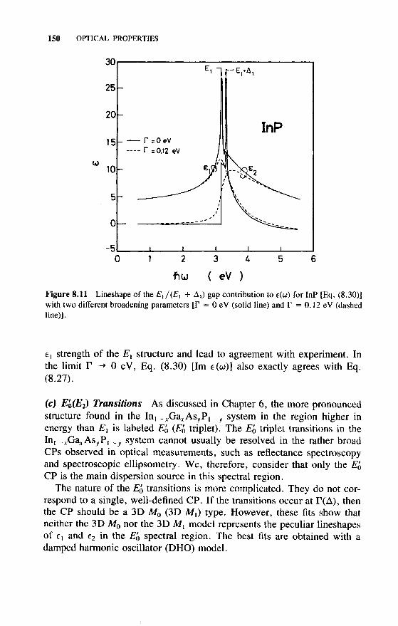
150 OPTICAL PROPERTIES
30
25
20
15
10
5
0
-5
E. n
r = 0 eVr =0.12 ev
InP
3 A 5 6
( eV )Figure 8.11 Lineshape of the £, /(£, + A,) gap contribution to e(o>) for InP [Eq. (8.30)]with two different broadening parameters [F = 0 eV (solid line) and F = 0.12 eV (dashedline)].
e, strength of the El structure and lead to agreement with experiment. Inthe limit r -> 0 eV, Eq. (8.30) [Im e(co)] also exactly agrees with Eq.(8.27).
(c) Ev(E2) Transitions As discussed in Chapter 6, the more pronouncedstructure found in the In^/ja^As^P, _y system in the region higher inenergy than £\ is labeled EQ (£Q triplet). The EQ triplet transitions in theInj./ja^ASyP, __y system cannot usually be resolved in the rather broadCPs observed in optical measurements, such as reflectance spectroscopyand spectroscopic ellipsometry. We, therefore, consider that only the EQCP is the main dispersion source in this spectral region.
The nature of the EQ transitions is more complicated. They do not cor-respond to a single, well-defined CP. If the transitions occur at T(A), thenthe CP should be a 3D M0 (3D M,) type. However, these fits show thatneither the 3D M0 nor the 3D Af, model represents the peculiar lineshapesof e, and e2 in the £Q spectral region. The best fits are obtained with adamped harmonic oscillator (DHO) model.

8.3 THE INTERBAND TRANSITION REGION 151
The DHO gives
(l - xl) -(8.32)
with
ftcoX2 = (8.33)
where C is the nondimensional strength parameter and 7 is the nondimen-sional broadening parameter. The calculated lineshapes of the DHO for InPare shown in Fig. 8.12. The numeric values are as follows: EQ = 4.72 eV,C = 1.30, and 7 = 0 (solid lines) and 0.093 (dashed lines). Note that in
20
15
10-
U)
-20
0
-5
-10|- Y = 0.093
-15
5 6( eV )
Figure 8.12 Lineshape of the EQ gap contribution to e(co) for InP [Eq. (8.32)] with twodifferent broadening parameters [7 = 0 (solid line) and y = 0.093 (dashed line)].

152 OPTICAL PROPERTIES
the limit 7 -* 0 the e} spectrum of the DHO is equivalent to the classicDrude-Lorentz formula: namely,
= ̂ \ ,2 (8-34)
(d) Indirect-Band-Gap Transitions It is well known that not only the di-rect transitions at the CPs but also the indirect transitions at the band gapinfluence the optical dispersion relations of semiconductors. The indirecttransitions in indirect-band-gap materials (e.g., GaP) take part at energiesbelow the onset of the direct transitions, and vice versa above the onset ofthe direct transitions in direct-band-gap materials (e.g., InP). Because in-direct transitions are higher order in the perturbation than direct ones, theirstrength is usually very weak, and one can expect to observe them only inspectra below the direct-threshold as a tail of the direct absorption edge inindirect-band-gap materials. However, previous work21 required a consid-erable strength of the indirect-band-gap contribution for analyses of e (co)spectra in both the indirect- and direct-band-gap materials.
The optical transition mechanism at the indirect band gap, £gD, is ex-pressed by a second-order process in the perturbation. This perturbationgives the contribution of the indirect transitions to e2(a>) as
- Xg) (8-35)
withEf ± h^
* = ̂ r^ (8-36)
where D is the strength parameter, huq is the energy of the phonons in-volved in the indirect transitions, and the H is a function defined by Eq.(8.28).
The parabolic bands extending to infinite energies implied by Eq. (8.35)should be nonphysical. One must, thus, modify the model by taking intoaccount a cutoff at energy Ec. This modification provides
~ Xc) (8.37)o))
withno)
Xc = TT (8.38)

8.3 THE INTERBAND TRANSITION REGION 153
Assuming that the strength parameter D is independent of the photonenergy, the KK transformation of Eq. (8.37) gives
2D ( (Eff (Ec \V1 - CM*ln (E?) + l + ln
(8.39)
Damping effects are not taken into account in both Eqs. (8.37) and(8.39). The e^co) spectrum of Eq. (8.39) therefore exhibits a divergence atEc (see Fig. 8.13). We thus introduce in these expressions a phenomeno-logic damping by replacing /ico by hu + iT. The contribution of the indirecttransitions to e(co) is finally given by21
2D ( (Ef)2 / E 1_
e(o>) = — - InTT (^ (hu + *T)2 "" \EfJ 2 V * ' ho) +
f^ , -T^ , r? 1 / /7lD \ 2HCO + II H- ,Cr I / ^g \
In _ + r I - T ^-^ In-f iT + Ef 2 \ hu + iTj hu + iT - Ef
(8.40)
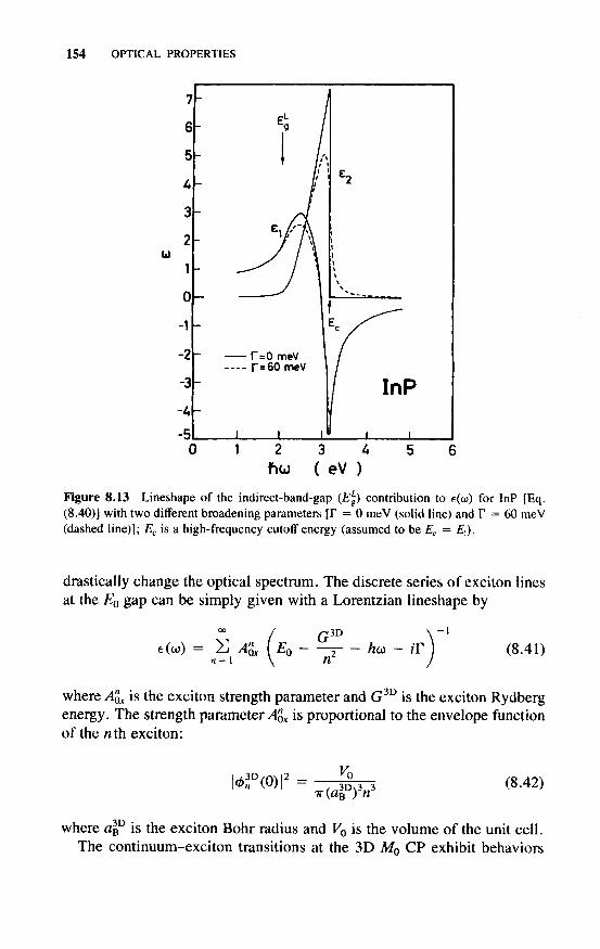
In Fig. 8.13 we show e(co) spectra calculated from Eq. (8.40) for InP.The numeric parameters used are EL
% — 2.05 eV, Ec = 3.16 eV (= E } ) , D= 60.4, and F = 0.06 eV. It is evident from the figure that the e} spectrumexhibits no clear structure at the indirect edge El®(Eg). It is also note-worthy that in the limit F -» 0 eV the calculated e2 spectrum agrees exactlywith that predicted by Eq. (8.37).
(e) Excitons and Exciton Parameters At low temperatures, optical spec-tra may not be explained within the framework of the one-electron approx-imation used in the above subsections [(a)-(d)], since the excitonic effectmay profoundly modify the CP singularity structure at low temperatures.Excitonic states should, in principle, exist at each type of CP, because aCoulomb-like interaction is always present between electrons and holes.There are many theoretical papers dealing with excitonic effects on opticalspectra of semiconductors.29'41
Let us present the contribution of exciton transitions to e (co) at the lowestdirect band edge. It is well known28'30 that the discrete lines and continuumexcitons in the neighborhood of the lowest direct band edge (3D M0 CP)
154 OPTICAL PROPERTIES
7
6-
U
3
2
1
0
-1 -
-2-
-3-
-5
InP
3( eV )
Figure 8.13 Lineshape of the indirect-band-gap (Eg) contribution to c(w) for InP [Eq.(8.40)] with two different broadening parameters [F = 0 meV (solid line) and F = 60 meV(dashed line)]; Ec is a high-frequency cutoff energy (assumed to be Ec = £",).
drastically change the optical spectrum. The discrete series of exciton linesat the £"0 gap can be simply given with a Lorentzian lineshape by
e(co) =n= 1
G3D
EQ 2" - /KO - IT (8.41)
where ̂ is the exciton strength parameter and G3D is the exciton Rydbergenergy. The strength parameter AQX is proportional to the envelope functionof the nth exciton:
(8.42)
where a™ is the exciton Bohr radius and V0 is the volume of the unit cell.The continuum-exciton transitions at the 3D M0 CP exhibit behaviors
8.3 THE INTERBAND TRANSITION REGION 155
like noninteracting electron-hole pair characteristics. The contribution ofthese transitions to e(o>) can, therefore, be expressed by an expression sim-ilar to Eq. (8.21).
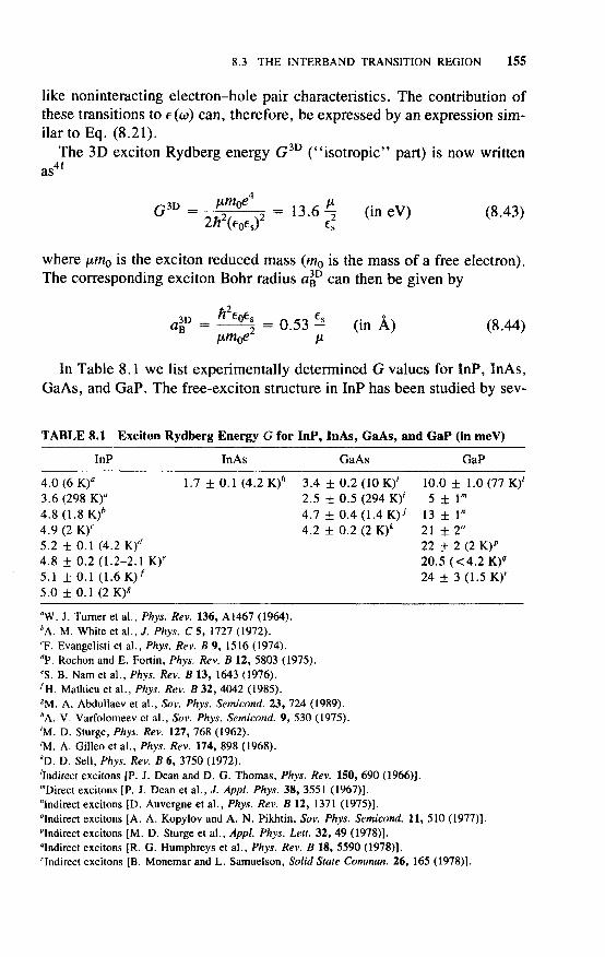
The 3D exciton Rydberg energy G3D ("isotropic" part) is now writtenas41
C3D = ~, = 13.6 (in eV) (8.43)es
where /iW0 is the exciton reduced mass (m0 is the mass of a free electron).The corresponding exciton Bohr radius a^ can then be given by
ft2" €= 0.53 - (in A) (8.44)
In Table 8.1 we list experimentally determined G values for InP, In As,GaAs, and GaP. The free-exciton structure in InP has been studied by sev-
TABLE 8.1 Exciton Rydberg Energy G for InP, InAs, GaAs, and GaP (in meV)
InP
4.0 (6 K)a
3.6 (298 K)a
4.8(1.8K) f e
4.9 (2 K)c
5.2 ± 0.1 (4.2 Kf4.8 + 0.2(1.2-2.1 K)e
5.1 + 0.1 (1.6 K)/
5.0 ± 0.1 (2K)*
InAs GaAs
1.7 ± 0.1 (4.2 K)* 3.4 ± 0.2 (10 K)'2.5 ± 0.5 (294 K)'4.7 ± 0.4(1. 4 KV4.2 ± 0.2 (2 K)*
GaP
10.0 ± 1.0(77K)'5 ± r
13 ± 1"21 ± 2°22 ± 2 (2 K)p
20.5(<4.2K)«24 ± 3(1.5K) r
"W. J. Turner et al., Phys. Rev. 136, A1467 (1964).bA. M. White et al., J. Phys. C 5, 1727 (1972).T. Evangelist! et al., Phys. Rev. B 9, 1516 (1974).dP. Rochon and E. Fortin, Phys. Rev. B 12, 5803 (1975).fS. B. Nam et al., Phys. Rev. B 13, 1643 (1976).f H . Mathieu et al., Phys. Rev. B 32, 4042 (1985).*M. A. Abdullaev et al., Sov. Phys. Semicond. 23, 724 (1989).*A. V. Varfolomeev et al., Sov. Phys. Semicond. 9, 530 (1975).'M. D. Sturge, Phys. Rev. 127, 768 (1962).JM. A. Gilleo et al., Phys. Rev. 174, 898 (1968).*D. D. Sell, Phys. Rev. B 6, 3750 (1972).'Indirect excitons [P. J. Dean and D. G. Thomas, Phys. Rev. 150, 690 (1966)]."Direct excitons [P. J. Dean et al., J. Appl. Phys. 38, 3551 (1967)]."Indirect excitons [D. Auvergne et al., Phys. Rev. B 12, 1371 (1975)].Indirect excitons [A. A. Kopylov and A. N. Pikhtin, Sov. Phys. Semicond. 11, 510 (1977)].indirect excitons [M. D. Sturge et al., Appl. Phys. Lett. 32, 49 (1978)]."Indirect excitons [R. G. Humphreys et al., Phys. Rev. B 18, 5590 (1978)].indirect excitons [B. Monemar and L. Samuelson, Solid State Commun. 26, 165 (1978)].

156 OPTICAL PROPERTIES
eral investigators.42"48 Turner et al.43 observed sharp peaks in intrinsic ab-sorption coefficient data for undpoded InP at 6 and 77 K. From these datathey determined that the exciton Rydberg energies are 4.0 ± 0.2 meV at6 K and 3.6 ± 0.4 meV at 298 K. White et al.,44 using photoluminescencemeasurements on high-quality epilayers, determined the Rydberg energy inInP to be 4.8 meV at 1.8 K. Reflectance spectra for pure InP have beenreported by Evangelisti et al.45 The G value they obtained is 4.9 meV.Photovoltaic spectra measured by Rochon and Fortin42 for w-type InP alsogive G = 5.2 ±0.1 meV. Nam et al.46 have determined the exciton Ryd-berg energy tobeG = 4 .8±0.2 meV and the reduced mass of the excitonto be JJL = 0.052. Mathieu et al.47 have recently investigated the reflectivityspectra of InP at normal incidence, at 1.6 K, and under [100] uniaxialstress. They found three transverse exciton energies associated with the Is(n = 1) ground state and the 2s (n = 2) and 3s (n = 3) excited states. Theydetermined the exciton Rydberg energy G = 5.1 ± 0.1 meV, exchangeenergy A = 0.04 ± 0.02 meV, and longitudinal-transverse splitting £LT
= 0.17 ± 0.02 meV by resolving the fine structure of the exciton states.The surface dead layer corresponding with the best experimental fit wasfound to be twice the exciton Bohr radius, as expected for an intrinsic ex-citon-free surface layer. More recently, Abdullaev et al.48 studied an ex-citon structure at the absorption edge of high-purity epitaxial InP films at2 K. They found the Rydberg energy G* = G + AG( = 5.0 ± 0.1 meV)where G(=4.82 meV) is the "isotropic" part given by Eq. (8.43) andAG(=0.17 meV) is the "anisotropic" correction found from perturbationtheory.41
Since es in Eq. (8.43) is a relatively strong function of the temperature71, the Rydberg energy G is also a function of T. As mentioned in Section5.1, the values of es for semiconductors usually decrease with decreasingT. For InP a value of es = 12.56 ± 0.2 was obtained at T = 300 K andan extrapolated value of 11.93 ± 0.2 was obtained at T = 77 K.49 Assum-ing fji~{ = (ml/Wo)'1 + (w^/mor1 and m^/m0 = 0.079 and mhh/m0 =0.46 for InP (see Section 6.2), we calculate G = 5.8 meV at T = 300 Kand 6.4 meV at T = 77 K. These values are considerably larger than thosedetermined experimentally (3.6 ± 0.2 meV at 298 K and 4.0 + 0.4 meVat 77 K43). If we assume n~l = (ml/m0)~
l + (mlh/m0)~l and w,h/ra0 =
0.120 for InP (also see Section 6.20), agreement is better (G = 4.1 meVat 300 K and 4.6 meV at 77 K).
In Fig. 8.14 we show the interpolated G as a function of y forIn, _^Ga^As^P, _ y lattice-matched to InP. The end-binary data used are 4.8meV for InP,44'46 1.7 meV for InAs,50 4.2 meV for GaAs,51 and 5 meVfor GaP.52 The calculated curve, as a function y, is given by the quadratic

8.3 THE INTERBAND TRANSITION REGION 157
10
8
! 6
SO
I i i
0.5y
1.0
Figure 8.14 Three-dimensional exciton Rydberg energy G3D as a function of y forIn| _ rGar AsvP, _ v lattice-matched to InP. The experimental data are taken from Table 8.1(InP), from Refs. 53 (solid circle), 54 (open circle), and 63 (open triangle). The solid lineshows the interpolated result of Eq. (2.3) using the end-binary data (InP,44'46 InAs,50 GaAs,51
and GaP52).
form (in millielectron volts):
= 4.8 - 2.9y + l.O/ (8.45)
Satzke et al.53 have studied optical absorption of anI^ ./ja^As^P, _y/InP double heterostructure (y — 0.65). Although nodiscrete exciton levels were observed even at low temperatue (10 K), anexciton Rydberg energy of 2.3 meV is obtained from the continuum statesby fitting the spectrum with a Lorentzian function. The steepness of theabsorption at the band edge provided a value of 4 meV for the continuum-exciton linewidth. This value is larger than the Rydberg energy and ex-plains why no discrete exciton levels are observed. The solid circle in Fig.8.14 is the plot of their determined G value. The corresponding excitonreduced mass n/m0 is 0.029. They also considered that this reduced massis in good agreement with the value of 0.030 derived from an electron massof 0.051 and a light-hole mass of 0.07 reported for material of similarcomposition.
Chen and Kim54 have observed a free exciton absorption peak in thetransmission spectra of In0 53Gao.47As and determined an exciton Rydbergenergy of 2 ± 1 meV at 5 K for this alloy. Their result is plotted in Fig.8.14 by the open circle. Adding the measured Rydberg energy to the ex-

158 OPTICAL PROPERTIES
citon absorption peak energy, they determined the E0 gap energy ofIno.saGao^As at 5 K to be 0.819 ± 0.0015 eV. At 77 K, the exciton peakwas still resolved in the absorption spectrum. From the position of theexciton absorption peaks a band-gap energy shift of 4 meV was determinedfor In0 53Gao.47As between 5 and 77 K.
Detailed absorption measurements on In0 53Ga0.47As have also been car-ried out in the temperature range between 5 and 340 K by Zielinski et al.55
They observed free exciton peaks in the range between 5 and 100 K. Theexciton parameters derived at 5 K are EQ = 0.8215 + 0.0002 eV, G = 2.5± 0.3 meV, F = 5.1 ±0.3 meV, and P2 = 20.7 ± 1 eV (squared mo-mentum matrix element). Their G value is also plotted in Fig. 8.14 by theopen triangle.
In Fig. 8.15 we show the spectral dependence of the absorption coeffi-cients a(co) in the neighborhood of the £0 edge of InP. The open circles arethe measured spectra taken from Ref. 43 (T = 6, 77, 298 K). The solidlines represent the calculated results taking into account the discrete excitonstates [i.e., Eq. (8.41)]. The numeric parameters used are E0 = 1.421 eV,G = 4.8 meV, T = 5.3 meV, and A^ = 3 x 10~3 eV (A^ = A^/n3) at6 K, and E0 = 1.414 eV, G = 4.6 meV, T = 5.4 meV, and A^ = 3 x10~3 eV at 77 K. The broadening parameters T determined here are foundto agree well with those presented in Fig. 6.13.
There may be only two analytic expressions that enable us to treat theexcitonic effects at the El/(El + A,) spectral region: (1) the effective-mass(EM) approximation32'33 and (2) the Koster-Slater (KS) method.34'36
2*x
^ 13-?§ 12»>
11
10
9-
87
,0° 298K
InPCalculated
1.34 1.36 1.38 1.40 1.42 1.44 1.46hu ( eV )
Figure 8.15 Spectral dependence of a(co) in the neighborhood of the E0 edge of InP asreported by Turner et al.43 The solid lines show the numerically calculated results takinginto account the discrete exciton series [i.e., Eq. (8.41)].

8.3 THE 1NTERBAND TRANSITION REGION 159
In the case of the 3D M\ CPs (i.e., the saddlepoint excitons or hyperbolicexcitons), the EM equation is much more difficult to solve. However, inthe limit mf ! ~ 0 the equation predicts a series of the 2D Wannier-typeexcitons32
(n - j)2
£2A = £| + A, -— (8.46b)(n - ±)2
where G2D(G2iD) is the 2D-exciton Rydberg energy. The contribution of
the 2D-exciton transitions to c(co) is written with a Lorentzian lineshape as
= Z \B[X(E% - *« - iry1 + B^E™ - too - iT)-1] (8.47)
where Bnlx(B^x) is the exciton strength parameter proportional to the enve-
lope function of the nth exciton. The envelope function can now be givenby
<8'48>- if
In Eq. (8.48) a2*0 is the 2D-exciton Bohr radius. The 2D EM approximationalso gives the continuum part of the excitonic states.32 One can, however,consider that the contribution of this part is similar to that of the one-elec-tron approximation [i.e., Eq. (8.30)].
In the KS method, the electron-hole interaction (Coulomb potential) isevaluated in the tight-binding approximation (TBA) and its attraction isapproximated by an on-site contact interaction. An approximate expressionof e(co) based on this model is written as34'36
(8'49)IT1 - g[e(co) - 1]
where e is the one-electron dielectric function and the parameter g is pro-portional to the depth of the assumed square- well potential. This expressionwas successfully used to show the presence of the excitonic effects in theEI structure of low-temperature electroreflectance data of Ge.34

160 OPTICAL PROPERTIES
As we can see in Refs. 56 and 57, optical spectra in the El/(E{ + A,)structure region of InP and GaAs become sharp when the temperature islowered. Such a spectral change cannot be explained within the frameworkof the one-electron approximation with lifetime broadening corrections.This fact clearly suggests evidence for the contribution of the excitoniceffects to the El/(El + A,) transitions. Not only the EM approximationbut also the KS method dramatically modifies and sharpens the £,/(£", +AI) CP structure. The degree of sharpness is, however, larger for the EMapproximation than for the KS method.57 We find better agreement withthe experiment using the EM approximation.
Multiparticle effects on CPs in the interband continuum of semiconduc-tors with their detailed electronic-energy band structures have beentreated.38'39 Results have shown that by introducing the excitonic interac-tion the absorption at £0(^2) CP is markedly reduced with no drastic changein its shape. Unfortunately, however, no analytic lineshape suitable forfitting the excitonic-effect-influenced £Q lineshape has been reported todate. In Refs. 56-59 the DHO model of Eq. (8.32) is found to be a goodrepresentation for the £"0(^2) CP both with and without the presence ofexcitonic interaction. The strength parameter C in this expression may, inprinciple, be independent of the temperature. Thus, a change in C valuescan account for the excitonic interaction strength at the £$(£2) CP in semi-conductors.56'59
8.3.2 Experimental el and e2 Spectra
Spectroscopic ellipsometry is known to be highly suitable for investigatingthe optical response of semiconductors over a wide range of photon ener-gies.60 This technique is very surface-sensitive, but the surface-contami-nation effects can, in principle, be mathematically removed in the analysis.Aspnes and Studna61 have measured room-temperature optical constants ofundoped InP at energies between 1.5 and 6.0 eV by spectroscopic ellip-sometry. They have presented numeric information on the optical con-stants, €[ , e2> n> k> R> and a, in tabular form. Their results illustrate theimportance of proper sample preparation and the capability of separatelydetermining both e{ and e2 in optical measurements.
Lautenschlager et al.62 have measured the temperature dependence ofthe dielectric function, c = €| -f- ic2, of compensated, high-resistivity InPin a temperature range between 30 and 750 K and a photon-energy rangebetween 1.3 and 5.5 eV by spectroscopic ellipsometry. The structures ob-served in the e spectra were attributed to interband CPs that can be analyzed

8.3 THE INTERBAND TRANSITION REGION 161
in terms of the following standard analytic lineshapes:
e(co) = C0 - AQe*(ha - ECP + iT)n (8.50)
They determined the CP parameter amplitude A0, energy threshold ECP,broadening T, and excitonic phase angle 0 for each CP [£"0, EO + A0, £,,£, + A,, and EQ/(£Q + A')] by fitting the numerically obtained second-derivative spectra d2e(ut)/du2 of the experimental e(co). Unfortunately,however, these expressions are not suitable for describing the dielectricbehavior e(co) over the entire range of photon energies.59
The dielectric functions of high-purity InP and In0.53Gao.47As layersgrown by metal-organic vapor-phase epitaxy have been measured by Er-man et al.63 in the 2.0-3.5-eV range using spectroscopic ellipsometry. Theydemonstrated that the ellipsometry technique can provide a useful, nonde-structive, and rapid assessment of the In0.53Gao.47As/InP heterostructurequalities. The analysis of the data using the multilayer modeling gave in-formation on the chemical nature and the thickness of the interface region.The sharpest interface as measured by this modeling was 30 A of InGaAsPat the interface of InP grown on In0 53Gao.47As and 9 A of InAs forIn0 53Gao 47As grown on InP.
Burkhard et al.64 have measured n and a of In, .^Ga^As^P, _y lattice-matched to InP (0 g y ^ 1.0) and of GaAs and GaP by ellipsometry inthe wavelength range between 0.365 and 1.1 /zm. High-quality layers weregrown by liquid-phase epitaxy (LPE). They also determined the thicknessdox of the temporal growth of the natural oxide layer on various InP andGaAs samples by the ellipsometry. The increase of dox for InP was foundto be 3.9 A for every factor of 10 increase in time when measured inminutes.
Kelso et al.26 have ellipsometrically measured high-precision pseudodi-electric function spectra from 1.5 to 6.0 eV of Ini .^Ga^As^P, _y lattice-matched to InP. A series of In, _JCGaJCAs>;P1 _ y samples that covered therange y — 0 to 1.0 were grown by LPE. Each layer had a thickness largerthan or equal to 1 /xm. The compositions were determined from X-ray mea-surements and room-temperature photoluminescence spectra and should beaccurate to ±0.02 for y. As mentioned in Section 6.1, they assigned thefeature previously attributed E2 in InP to £Q(£O + AQ).
Knowledge of the structure, on the atomic scale, of the interface re-gion between various layers is important for understanding the electronicproperties of heterostructures. High sensitivity makes spectroscopicellipsometry a useful tool for addressing heterostructure problems. Thishas been illustrated by an investigation of the structural nature of

162 OPTICAL PROPERTIES
Al/ja^^As/GaAs65 and In^Gao^As/InP heterojunctions.63 Similarwork on In! _^Ga^AsyPi -y/lnP heterojunctions has been made by Drev-illon et al.66 using polarization-modulation spectroscopic ellipsometry. Themeasured spectral range was 1.5-5.3 eV, and the optical-constant data ob-tained agreed with the results of Kelso et al.26 They compared the steepnessof the heterojunctions between two types of structures: those produced bythe growth of In! .^Ga^As^P, _y (or Ino.53Gao 47As) on InP and those ob-tained by the reverse growth sequence. The sharpest interface was achievedfor InP growth on quaternary where the interface region was estimated tobe 10 ± 10 A thick.
The data of Kelso et al.26 and Drevillon et al.66 are very useful for un-derstanding fundamental optical properties of the Ini __xGaxAsyPi _ y alloy.These data seem to have one disadvantage, however; they are not expressedas continuous analytic functions of photon energies.
The fits with the dielectric-function model proposed here to the experi-mental e2(co) and €i(o>) spectra of InP at 300 K are shown in Figs. 8.8 and8.9, respectively. The solid circles represent the spectroscopic-ellipsome-try data of Kelso et al.26 The solid lines were obtained from the sum of Eq.(8.21) (Fig. 8.10), Eq. (8.30) (Fig. 8.11), Eq. (8.32) (Fig. 8.12), Eq.(8.40) (Fig. 8.13), and Eq. (8.47). The 2D exciton strength and broadeningparameters determined by these fits are B\x — 1.00 eV, B\x = 0.25 eV,and r[E, /(£", + A!)] = 0.12 eV. Since the 2D ground-state exciton term(n = 1) in Eq. (8.47) contains 95% of the total oscillator strength, one canneglect the excited-state terms (n > 2) in the calculation. The 3D discrete-exciton states may also be present only in the limited region close to the£"0 edge, and their strength is considerably weaker than those of the ensur-ing £*!, E{ + A,, and EQ. The contribution of these states is thus not soimportant, and can be neglected in the analysis.
As seen in Fig. 8.8, the transitions at the M0 edges [EQ/(EQ + A0)] yielda continuous absorption obeying the well-known |-power law [i.e., oc (hu— £o)0'5]. The transitions at the Eg gap provide a gradually increasingabsorption spectrum characterized by a power law of (fio> - Eg)2. Becauseof the low probability for indirect transitions, one can realize them only inthe spectral region between Eg and E{. The E{ and E{ + A, gaps are ofthe 3D MI (2D M0) type. Hence, the lineshape of corresponding e2 spec-trum [Eq. (8.30)] should be characterized by a steep low-energy side anda less steep high-energy side, in good agreement with the experimentaldata. Introduction of the damping effect into Eq. (8.30) can successfullydecrease the strength of the E\ and E, + A, peaks (see Fig. 8.11) andproduces a result that agrees with experiment (F = 0.12 eV). The experi-mental €2 spectrum shows a relatively strong, symmetric peak in the EQ CPregion. This peak can be interpreted well by the DHO model of Eq. (8.32).

8.3 THE INTERBAND TRANSITION REGION 163
It is also evident that the strong negative peak of e, observed in the E'Qstructure region can be interpreted well by the DHO model (see Fig. 8.9).
We show in Figs. 8.16 and 8.17 our calculated e2(co) and e,(co) spectraof In0.53Gao.47As at 300 K compared with experimental data. The experi-mental data are taken from Refs. 25 (open circles, Fig. 8.16), from 26(solid circles, Figs. 8.16 and 8.17), and from 27 (open circles, Fig. 8.17).The solid lines are the results of the sum of Eqs. (8.21), (8.30), (8.32),(8.40), and (8.47). The numeric parameters used are as follows: EQ
= 0.75eV, £0 + A0 = 1.04 eV, A = 1.20 eVl 5, T[E0/(E0 + A0)] = 15 meV,£, =2.57eV,E, + A, =2.83eV,B1 = 3.84eV,B2 = 1.48eV, T[E0/(EQ
+ A0)] = 0.12 eV, B\x = 0.90 eV, B1^ - 0.35 eV, T(2D exciton) = 0.12eV, ££ = 4.41 eV, C = 2.90, y = 0.225, fi£ = 1.20 eV, D = 20.7, and
= 0.06 eV.
100
10
CMU)
0.1
0.012 3 4 5 6
tiu ( eV )8 9
Figure 8.16 The e2 spectrum of II\Q 53Gao.47As (300 K). The solid line shows the result ofthe sum of Eqs. (8.21), (8.30), (8.32), (8.40), and (8.47). The experimental data are takenfrom Refs. 25 (open circles) and 26 (solid circles). The vertical arrows indicate the positionsof each CP and Eg gap that play an important part in the calculation of the e2 spectrum.(From Adachi.16)

164 OPTICAL PROPERTIES
30
25
20
15
10
uT 5
0
-5
-10
-15
-20
In0.53GV7AS
2f)U)
3(eV )
Figure 8.17 The e, spectrum of Irio 53Gao.47As (300 K). The solid line represents the resultof the sum of Eqs. (8.21), (8.30), (8.32), (8.40), and (8.47). The experimental data aretaken from Refs. 27 (open circles) and 26 (solid circles). The vertical arrows indicate thepositions of each CP and Eg gap that play an important part in the calculation of the €|spectrum. (From Adachi.16)
It is clear that the 3D A/0 term [Eq. (8.21)] and the indirect-band-gapterm [Eq. (8.40)] interpret the 0.75-3.0-eV region of the e2 spectrum well.The calculated value of e2 at the E2 peak is 19.1, in good agreement withthe experimental value (19.3). As in the case of InP, we see a better fit ofour e j model to the experimental data over the entire range of photon ener-gies.
As mentioned in Section 8.3.1, the dielectric function is expressed bythe electronic energy-band parameters (band-gap energies) and the corre-sponding strength and broadening parameters. In Ref. 16 such parametersfor Inj .^GajASyPj _y lattice-matched to InP are specified in terms of yalone. Using these results, we can easily calculate the spectral dependenceof e{ and e2 for an optional composition of the In! _xGaxA^yP} _y quater-nary. The temperature dependence of e(o;) for InP was also analyzed by the

8.3 THE INTERBAND TRANSITION REGION 165
same method.56 The excitonic effects accounted for the discrepancies in thee2 strengths of the £, and £Q peaks in InP; thus, the inclusion of the exci-tonic effects in the one-electron band model changed the strength of thepeaks in the correct direction to agree with the experimental result (it ledto strengthening of the El peak and weakening of the EQ peak).
8.3.3 Dispersion of the Refractive-Index, Extinction, andAbsorption Coefficients
The analysis presented in Section 8.3.2 is based on a simplified model ofthe energy-band structure of the materials. The model covers the e(co) spec-tra of the materials in the entire range of photon energies. These resultsprompt us to apply the model to other important optical constants for prac-tical-device engineering that are related to the dielectric function [such asthe refractive index (n), extinction coefficient (&), absorption coefficient(a), and normal-incidence reflectivity (/j)].20'22>24<67>68
Figure 8.18 shows the experimentally determined n and k for InP at 300K. The data are taken from Refs. 69 (open-circles) and 61 (solid circles).
0
InP
3 A
( eV )
Figure 8.18 Numerically calculated spectral dependence of n and k for InP (300 K). Thesolid and open circles show the experimental data taken from Refs. 61 and 69, respectively.(From Adachi.68)

166 OPTICAL PROPERTIES
The solid lines show the numerically calculated spectral dependence of nand k for InP. They are obtained from Eq. (8.5) for n and from Eq. (8.6)for A:.
The strongest peak in n at —3.1 eV is related mainly to the E} transi-tions. The experimental value of this peak is about 4.4. The calculation ofEq. (8.5) gives n = 4.38, in good agreement with this value. In /:, thespectrum above ~ 1.4 eV is associated with the onset of the E0/(E0 + A0)transitions. The strongest peak in k occurs at -4.8 eV. This peak is relatedto the £"0(^2) transitions.
A comparison of the experimental data of a61 with our calculated valuesfor InP at 300 K is shown in Fig. 8.19. The solid line is calculated fromEq. (8.7). Since InP is a direct-band-gap semiconductor, the indirect tran-sitions (£g) take part above the onset of the direct transitions that occur at1.35 eV (£"o). If we do not take into account the EL
% gap contribution, thefit with the experiment becomes very poor in the 2-3-eV region. The the-
10'
10'
Iff
InP
2flU)
3 4
( eV )
Figure 8.19 Numerically calculated spectral dependence of a for InP (300 K). The ex-perimental data (solid circles) are taken from Ref. 61. (From Adachi.68)
8.3 THE INTERBAND TRANSITION REGION 167
oretical £\ contribution provides a plateau-like lineshape in a, in goodagreement with experimental results. The strongest peak in a occurs at-4.8 eV. This peak can be successfully interpreted by the £o-gap contri-bution.
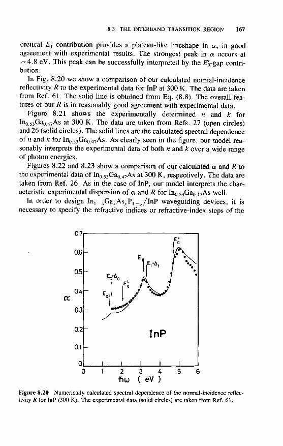
In Fig. 8.20 we show a comparison of our calculated normal-incidencereflectivity R to the experimental data for InP at 300 K. The data are takenfrom Ref. 61. The solid line is obtained from Eq. (8.8). The overall fea-tures of our R is in reasonably good agreement with experimental data.
Figure 8.21 shows the experimentally determined n and k forIn0.53Ga0 47As at 300 K. The data are taken from Refs. 27 (open circles)and 26 (solid circles). The solid lines are the calculated spectral dependenceof n and k for Ino 53Ga0 47As. As clearly seen in the figure, our model rea-sonably interprets the experimental data of both n and k over a wide rangeof photon energies.
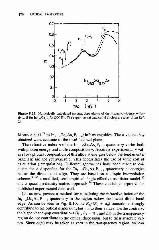
Figures 8.22 and 8.23 show a comparison of our calculated a and R tothe experimental data of In0 53Ga0 47As at 300 K, respectively. The data aretaken from Ref. 26. As in the case of InP, our model interprets the char-acteristic experimental dispersion of a and R for In0.53Gao.47As well.
In order to design In, _xGaxAsyP{ _^/InP waveguiding devices, it isnecessary to specify the refractive indices or refractive-index steps of the
0.7
0.6
0.5
QA
0.3
0.2
0.1
InP
I I3 A( eV )
Figure 8.20 Numerically calculated spectral dependence of the normal-incidence reflec-tivity R for InP (300 K). The experimental data (solid circles) are taken from Ref. 61.

168 OPTICAL PROPERTIES
7i
1 -
3 4 5 6( eV )
Figure 8,21 Numerically calculated spectral dependence of n and k for Ino 53Ga0.47As (300K). The solid and open circles are the experimental data taken from Refs. 26 and 27,respectively. (From Adachi.68)
heterojunction structures. In the energy region below the fundamental ab-sorption edge, where the material is nearly transparent, the n measurementswere carried out for InP by a prism method70'71 and by a near-Brewster-angle reflectivity method72'73 and for In^Ga^As ternary (x > 0.53) bysurface reflection.74
Chandra et al.75 have presented n data for In, ,xGaxAsyPl ,y layers withy between 0.276 and 1.0 taken as a function of the wavelength from 2.5pm to about 0.1 /mi below their respective absorption edges. Interferencefringes were the basis of the measurements. The layers were grown by HC1-transport vapor-phase epitaxy on (001) InP and were unintentionally doped.Broberg and Lindgren73 have also measured the n values ofIn, ̂ Ga,. As^P, _y layers on (001) InP using a Brewster-angle method. Thelayers used were all undoped. The compositions of the layers were in therange 0-0.742 and were determined by electron microprobe X-ray analysis.The measurements were made at the wavelengths X = 1.15, 1.30, and 1.55jun. These wavelengths are of particular interest for optical fiber commu-nication systems. They have also found that a lattice mismatch variation of10~3 corresponds to a change in n of approximately 0.02 for a y = 0.474layer at X = 1.3 /xm. The n dispersion in the near-band-gap region of

8.3 THE INTERBAND TRANSITION REGION 169
10
106
105
103
0( eV )
Figure 8.22 Numerically calculated spectral dependence of a for In0 53Ga0.47As (300 K).The experimental data (solid circles) are taken from Ref. 26. (From Adachi.68)
In, .^Ga^As^P, _ y quaternary has also been determined by Kowalsky etaj 25,76 from transmission and reflection measurements.
A new method of detecting optical waveguide modes of semiconductorepitaxial layers was developed by Henry et al.,77 who applied it toIn, ./ja^As^P, _y layers lattice-matched to InP. The modes were excitedby photoluminescence and coupled out of the semiconductor wafer by agrating etched on the surface of the guiding layer. The quaternary layersstudied were grown by two-phase LPE, and were of eight different com-positions. This method was used to measure the n dispersion in the trans-parent region and also the change in the mode index of a laser in goingfrom low current up to threshold.
A diffraction grating formed on an InP substrate has also been used byFronts et al.78 for measuring the refractive index of In, _^Ga^As^P, _y atthe wavelength for stimulated emission. It is possible to determine the re-fractive index of a guiding layer by measuring the cutoff wavelengths ofthe supported modes in a waveguide. This method has been applied by
170 OPTICAL PROPERTIES
0.7,
0.6
0.5
OA
0.3
0.2
0.1
3 4 5 6
( eV )
Figure 8.23 Numerically calculated spectral dependence of the normal-incidence reflec-tivity R for Ino 53Gao 47As (300 K). The experimental data (solid circles) are taken from Ref.26.
Morasca et al.79 to In, _^Ga^AsyP, _y/InP waveguides. The n values theyobtained were accurate to the third decimal plane.
The refractive index n of the In, _JCGaJCAsyP, _y quaternary varies bothwith photon energy and mole composition y. Accurate experimental n val-ues for optional composition of this alloy at energies below the fundamentalband gap are not yet available. This necessitates the use of some sort ofcalculation (interpolation). Different approaches have been made to cal-culate the n dispersion for the In, ^Ga^As^P, _y quaternary at energiesbelow the direct band edge. They are based on a simple interpolationscheme,80"82 a modified, semiempirical single-effective-oscillator model,83
and a quantum-density-matrix approach.84 These models interpreted thepublished experimental data well.
Let us now present a method for calculating the refractive index of theIn, _^Ga^cAs>;P, _ r quaternary in the region below the lowest direct bandedge. As can be seen in Fig. 8.10, the EQ/(E0 + A0) transitions stronglycontribute to the optical dispersion, but not to their values. On the contrary,the higher-band-gap contributions (£",,£", + A,, and £Q) in the transparencyregion do not contribute to the optical dispersion, but to their absolute val-ues. Since e2(w) may be taken as zero in the transparency region, we can

8.3 THE INTERBAND TRANSITION REGION 171
successfully assume that
n(w) - [e,(co)]°5 (8.51)
The n((j)) in the transparency region can then be simply expressed, usingEq. (8.21), as27'85'86
(8.52)
where A* is the renewed strength parameter of the EQ and (E0 + A0) tran-sitions and 5* corresponds to the nondispersive contribution (i.e., constant)arising from the higher-lying band gaps, such as £,, E} + A,, ££, £"2» ^2+ A2, £J, and EJ 4- AJ . As seen in Figs. 8.9 and 8.17, our calculatedvalues of el are usually somewhat smaller than the experimental values overthe entire range of photon energies. This is because we cannot take intoaccount other, higher-lying gaps, such as £2> E2 + A2, E\9 and E\ + A|,in the calculations.
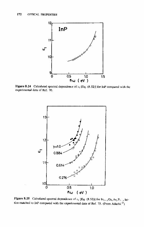
Chandra et al.75 have measured room-temperature n values for theIn! _xGaxAsyPl _y quaternary of target compositions y = 0-1.0 in incre-ments of 0.3 for wavelengths from 2.5 ^m to about 0.1 pm below theirrespective absorption edges. An attempt is made first to fit e(co)[=n(co)2]of Eq. (8.52) to the experimental data of Pettit and Turner70 and Chandraet al.75 Figures 8.24 and 8.25 show the calculated dispersion of e, [Eq.(8.52)] compared with the experimental data of Refs. 70 and 75, respec-tively. These comparisons show quite good agreement between calculationand experiment. The numeric values of A* and B*9 required to fit Eq. (8.52)with the experimental data, are shown as a function of y in Fig. 8.26. Theseresults provide
A*(y) = 8.40 - 3.40;y (8.53a)
B*(y) = 6.60 4- 3.40.y (8.53b)
The dielectric constant e^co), in other words fl(o>), of In! .^Ga^As^P, _ y
can then be specified in terms of y alone.Introducing Eq. (8.53) into Eq. (8.52) and using Eq. (8.51), we can
present the refractive indices for an optional composition of theIn^^Ga^As^?! __y quaternary. The calculated refractive-index dispersionof this system with j-composition increments of 0.1 is shown in Fig. 8.27.The impurities or, more generally, the lattice defects in semiconductors,reduce the lifetime of the excited electronic states, resulting in a change in
172 OPTICAL PROPERTIES
12
u
11
10
InP
0.5 1.0( eV )
1.5
Figure 8.24 Calculated spectral dependence of e, [Eq. (8.52)] for InP compared with theexperimental data of Ref. 70.
13
12
11 -
10
0.6U
0.276
0.5 1.0
flU) ( eV )
Figure 8.25 Calculated spectral dependence of e, [Eq. (8.52)] for In, ̂ Ga,AsyP, _y lat-tice-matched to InP compared with the experimental data of Ref. 75. (From Adachi.27)

8.3 THE INTERBAND TRANSITION REGION 173
Figure 8.26 Variation of A* and B*, re-quired to fit Eq. (8.52) with the experimen-tal data, versus y for In, .^ , _ v lat-tice-matched to InP. (From Adachi. )
3.7
3.6
3.5
3.4
3.3
3.2
3.1
3.0
y=1.0
I I I I I I
0.5 1.0
•hu ( eV )1.5
Figure 8.27 Calculated refractive indices of hi| .^Ga^As^ _,, as a function of the photonenergy with y-composition increments of 0.1. The solid and dashed lines represent, respec-tively, the results with T = 0 and T = 0.02E0.

174 OPTICAL PROPERTIES
optical properties. The refractive-index dispersion may be affected by thelifetime broadening (damping) F of the electronic states, especially in thephoton-energy region close to the band edge. The solid and dashed linesin the figure are, respectively, the results with F = 0 and F = 0.02£t
0- Itis obvious that the damping effect considerably reduces the n values at theE0 gap region. One must, therefore, pay attention to the analysis of therefractive-index dispersion in such a region.
8.4 FREE-CARRIER EFFECTS ON OPTICAL PROPERTIES
8.4.1 Optical Absorption
The optical absorption of interest here can be divided into three separateprocesses, which are shown in Fig. 8.28. The direct (indirect) transitionsfrom the valence band to the conduction band give rise to the absorptioncontribution avc (see Section 8.3). The normal free-carrier absorption aFC
depends on wavelengths approximately as
oc (8.54)
where m is dependent on various intraband scattering processes, that is, m= 2.5 limited by polar optical phonons (aop), m — 1.5 limited by acousticphonons (aac), and m = 3.5 limited by ionized-impurity scattering (aim).1
The final process of interest is the interconduction-band absorption acc. InFig. 8.29 we show schematic representation of these absorption coefficientsas a function of /ko near and below the intrinsic absorption edge.87 The o?Vcand acc takes part when hu > EQ(avc) and hu > A£'cc(acc). The apc
becomes significant at longer wavelengths.
Figure 8.28 Band-diagrammatic indication ofthe optical absorption in a semiconductor (avc>direct interband transition from the valence bandto the conduction band; acc, indirect intercon-duction-band transition; aFC, free-carrier intra-band transition).
vc

8.4 FREE-CARRIER EFFECTS ON OPTICAL PROPERTIES 175
AEcc Eo•ftto (log. scale) —-
Figure 8.29 Schematic representation of the absorption coefficient a in dependence onphoton energy #a> near and below the intrinsic absorption edge (avc» direct interband tran-sition from the valence band to the conduction band; o?cc, indirect interconduction-bandtransition; aop, free-carrier intraband transition involving optical phonons; c*ac, free-carrierintraband transition involving acoustic phonons; cxim, free-carrier intraband transition in-volving ionized impurities).
Near-band-gap absorption in InP-based semiconductors has been mea-sured by many authors (inp,43<48'88<89 In, _,GajcAs,P, _>,,25'53'76'90-94 andIn053Gao.47As54'55'95"98). Optical absorption in the free-carrier absorptionrange has also been measured for InP99"103 and In, _^Ga^ As.104 We will notattempt to review the considerable theoretical work on optical absorptionin the free-carrier absorption range,105 but will present the relevant exper-imental results.
As in the case of the refractive index (see Section 8.3.3), the absorptionspectrum in the vicinity of the fundamental edge is known to dependstrongly on crystalline quality. There may appear two prominent featuresin the fundamental-absorption-edge spectra of doped samples: (1) the wholeabsorption spectrum shifts to higher energies as the free-electron concen-tration increases (Moss-Burnstein shift) and (2) a pronounced absorptiontail appears (Urbach tail106) such that the Urbach parameter defined as f/0
= (d ln(a)/dE)~l increases with the doping concentration. Fornari andKumar107 have found that the absorption spectra in bulk Fe-doped InP differconsiderably from those recorded on undoped samples. Transition metals,

176 OPTICAL PROPERTIES
in particular Fe, are often used as dopants in order to obtain semiinsulatingproperties of InP108 and In0 53Gao.47As. 109 To understand whether the effectwas caused by the overall impurity concentration in the crystals rather thanby the nature of the impurity, they repeated the measurements on S- andSn-doped wafers. 107 We reproduce their results in Fig. 8.30. All three spec-tra are practically featureless at low energies (<7500 cm"1), but those forthe Fe-doped and undoped (or S-doped) samples differ considerably in thetail regions. The authors concluded that the tail in the Fe-doped samples isdue to absorption by Fe-related deep centers. They also determined thatthe absorption coefficient at 1 x 104 cm"1 can be taken as a sensitivemeasure of the Fe concentration and plotted the absorption coefficientagainst the Fe concentration (as determined independently with chemicalanalysis) to obtain a graph that is useful for routine characterization of Fe-doped InP crystals. Furthermore, the doping with Fe was found to give riseto considerable band-gap narrowing in this material.
The infrared absorption in InP has been studied as a function of free-carrier concentration in the spectral range from a few tens of micrometersto the fundamental absorption edge for both n-type99"102 and /?-type sam-ples.101'103 In Figure 8.31 shows a typical example for n-InP.102 The dataindicate that an absorption minimum exists at about 1.6 /xm, in agreementwith the results of Lorenz et al.99 and Dumke et al.100 At wavelengths X> 1 .6 jLtm free-carrier absorption dominates in the spectra. The dashed linein the figure gives a slope that is limited by ionized-impurity scattering
0.44
0.36
0.28
0.20
InP
10 9 8 7
PHOTON ENERGY (xlO3 cm1)
Figure 8.30 Absorption spectra of (a) undoped, (b) S-doped, and (c) Fe-doped InP. Theabsorption tail in the Fe-doped sample is due to absorption by Fe-related deep centers.(From Fornari and Kumar.10?)

8.4 FREE-CARRIER EFFECTS ON OPTICAL PROPERTIES 177
100
u 10
0.1 L
10
X (
Figure 8.31 Absorption coefficient a versus wavelength X for rc-type InP. The carrierconcentrations are 3,3 x 1Q16 cnT3 (#1), 4,0 X 1017 cm'3 (02), 8,8 X 1017 cm'3 (#3),and 5.0 x 1018 cm""3 (#4). The dashed line gives a slope that is limited by ionized-impurityscattering. (From Ballman et al.102)
[i.e., X oc (ftco)3'5]. The power index m taken with a heavily doped sample(#3) is about 3.5 (i.e., the dominance of ionized-impurity scattering). Ya-maguchi et al.101 also found that for rc-type InP m increases with increasingfree-electron concentration from about 2.0 (n — 1 x 1016 cm"3) to 3.5 (n— 1 x 1018 cm"3). For wavelengths near 1.3 jicm, the absorption coeffi-cients shown in Fig. 8.31 are still proportional to the free-electron concen-tration. This fact suggests the dominance of interconduction-band absorp-tion in this spectral region. Detailed studies of interconduction-bandabsorption in /i-InP has been carried out by Lorenz et al." and Dumke etal.100
The infrared absorption in p-type InP has been studied by several au-thors.101'103 Casey and Carter103 have measured the absorption spectra in/7-InP between wavelengths of 1.0 and 3.4 /xm for hole concentrations from

178 OPTICAL PROPERTIES
p = 3.1 X 10¹⁷ to 6.6 X 1018 cm 3 at 297 K. The spectra they obtainedare shown in Fig. 8.32. Ballman et al.102 have also measured infrared ab-sorption in lightly doped, /?-type InP (p = 6.0 x 1016 cm"3). Their resultis also shown in Fig. 8.32 by the dashed line. The figure clearly shows thatthe absorption coefficient increases as the hole concentration increase.Casey and Carter103 determined the concentration variation of the absorp-tion coefficient to be a = 14(p/1018 cm"3) cm"1 at a wavelength of 1.3pm and a = 20(/?/1018 cm"3) cm"1 at a wavelength of 1.5 /mi. Heatingto 100°C increased a by a measurable, although small, amount. Peaks thatappeared at about 0.4 eV (#1 and #2) are due to intervalence-band absorp-tion caused by transitions between the heavy-hole and the spin-orbit splitoffvalence bands [see Section 8.5 (Fig. 8.34)].
Aliev et al.104 have studied infrared absorption as a function of free-
400
100
10
0.1
»1
I I I 1 I
P-InPi i i i I I I
0.1 0.3 0.5 0.7 0.9 1.1 1.3 1.5
fiu ( eV )
Figure 8.32 Absorption coefficient a versus wavelength X forp-type InP. The solid anddashed lines represent the experimental data taken from Refs. 103 and 102, respectively.The carrier concentrations are 3.1 x 1017 cm'3 (#1), 8.6 x 1017 cm'3 (#2), 1.9 x 10¹⁸
cm'3 (#3), 5.3 x 10¹⁸ cirT3 (#4), 6.6 x 10¹⁸ cnT3 (#5), and 6.0 x 1016 cm~3 (dashedline).

8.4 FREE-CARRIER EFFECTS ON OPTICAL PROPERTIES 179
carrier concentration for n-type In, -xGax As (x < 0.1) at 92 and 300 K andfound that the absorption curves rise smoothly with wavelength and carrierconcentration. This is a typical characteristic of free-carrier absorption. Thepower indices obtained varied with alloy composition jc, carrier concentra-tion, and temperature (2.4 < m < 4.0). The experimental findings for thealloys were found to be in good agreement with the results obtained fromthe formula ex = <xdis + aInAs, where adis is an extra contribution of thealloy disorder to a as pointed out theoretically by Sieranski andSzatkowski110 and ainAs is the experimental value of the absorption coeffi-cient of the In As binary.
Rajalakshmi and Arora111 have analyzed the absorption spectra of Ge-doped In^^Ga^ASyPi _y lattice-matched to InP (y = 0.28) by includingan Urbach tail due to transitions from disorder-induced localized states atthe valence-band edge to the conduction band. Different types of disorderhave been taken into consideration in their analyses. The dependence ofthe absorption coefficients on electron concentration for a variety of com-positions in the Int _JCGa^As>,Pi -y/lnP system at a wavelength of 1.3 /xmhave been calculated by Fiedler and Schlachetzki,87 who used values forthe end-point binaries and took into account the Moss-Burstein band-gapshift. Brosson et al.112 have also shown that measurements of thresholdcurrent density and external quantum efficiency for a broad-area laser struc-ture lead to a determination of the carrier-induced optical loss and differ-ential loss. The differential loss they determined was da/dN = 1.1-2.3x 10" I 7cm2atX= 1.53 /mi in a \g = 1.30-^mn-Ini ./ja^As^P, _ r layer.
8.4.2 Carrier-Induced Change in Refractive Index
There has been an increasing interest in intensity and phase modulatorslately because of their importance in the development of integrated opto-electronics. Several authors have demonstrated light switches and modu-lators based on refractive-index changes in InGaAsP/InP heterojunctionp-n devices.113"115 The operation of these devices has been explained interms of the linear electrooptic effect and higher-order field effects115 or bythe effects of a free-carrier-induced change in the refractive index.113'114
The linear and nonlinear electrooptic effects change the refractive index inregions of the p-n device where high electric fields are present. Details ofthese effects will be presented in the next section. The free-carrier effectscan be classified into two categories: (1) a refractive index change that isbasically caused by free-carrier plasma dispersion (intraband free-carrierabsorption) and (2) a refractive-index change that originates from the changein the fundamental absorption gap (Moss-Burstein shift and/or band-gapshrinkage).

180 OPTICAL PROPERTIES
Intraband free-carrier absorption can be described, in the simplest way,in terms of the classic dispersion theory, which starts with an equation ofmotion for an electron of charge e and mass we( = w£ ; see Section 6.2.1)
we(;c + yx + coo*) = eEf exp(i'cof) (8.55)
with the damping constant 7, the restoring force meUQX, and the field of aelectromagnetic wave E = Ef exp(/cof). This leads to the following resultfor the dielectric constant1
/Ne2\ 1e(co) = 1 + - — - 2—— (8.56)
\mee0/ co0 - co + ryco
where N is the number of the electrons per unit volume. Here we can putc*>0 ~* 0, because there is no restoring force for free electrons. One can,then, obtain
c,(co) = 1 - —} —2 (8.57a)\mee0/ o>
/ ' Ne2\ v€2(«) = - - 1-3 (\me€0/ co3
If we replace co by cop and e, by e^ (i.e., the long-wavelength limit), Eq.(8.57a) provides a relation between the plasma frequency cop and the carrierconcentration given by Eq. (8.14). In the limit 7 -» 0 and using 2n An =Ac | [see Eq. (8.51)], we can obtain the change in the refractive index
8?r(8-58)
where c is the light velocity in the vacuum and X is the wavelength of light.Equation (8.58) suggests that the change An is directly proportional to X2,N, and (l/n). When both electrons and holes are present in a substance,as is usual for injection lasers, the change in n can be written, by modifyingEq. (8.58), as
<8.59)
where P is the number of holes per unit volume.

8.4 FREE-CARRIER EFFECTS ON OPTICAL PROPERTIES 181
A decrease in absorption for photon energies slightly above the funda-mental band gap can be observed for several semiconductors when they aredoped. This phenomenon, the so-called Moss-Burstein shift, is explainedby band filling and is partly compensated by band-gap shrinkage due tocarrier-carrier interactions at high concentrations. The relative contribu-tions of band filling, band-gap shrinkage, and free-carrier absorption to therefractive-index change An in InGaAsP/InP have been studied by Bottel-dooren and Baets116 and Bennett et al.117
In Fig. 8.33 we show a typical result for InP taken from Bennett et al.n?
Figure 8.330 illustrates the individual contributions to An of the band filling
0.15
0.8 1.0 1.2 U 1.6 1.8 2.0
10"
10
10'
10"
n-InP
fu*>=1.0-1.2eV
(b)
10 10 io19
ELECTRON CONCENTRATION (cm"3 )
Figure 8.33 Carrier-induced change in the refractive index: (a) predicted change in therefractive index An for InP (N = P = 3 X IO18 cm~3) from the band-filling (AnBF), band-gap shrinkage (AnBS), and free-carrier absorption (AnFA); (b) comparison of the calculatedand experimental An for n-type InP. The solid and dashed lines show the calculated results[A/r < 0 (solid lines) and An > 0 (dashed line)]. The solid circles show the experimentaldata. (From Bennett et al.117)

182 OPTICAL PROPERTIES
(A«BF), band-gap shrinkage (AnBS), and free-carrier absorption (AnFA) forInP with carrier concentrations A/r = /> = 3 x l O l 8 c m ~ 3 . The bold linerepresents the simple sum of these contributions. The curves for the AnBS
and ABS pass through zero at photon energies just above (AnBF) or below(AflBS) the direct band edge EQ undergoing a reversal in sign. The value of| A%A | increases gradually with decreasing photon energy because of itsX2 dependence [Eq. (8.59)]. Figure 8.33fo shows a comparison of the es-timated and available experimental An for n-InP at photon energies be-tween 1.0 and 1.2 eV. The prediction of Arc is seen to be in fairly goodagreement with the experimental data.
Whalen and Stone72 have measured the refractive index of /i-type InPsamples with carrier concentrations ranging from 1015 to 1019 cm~3 at thetwo wavelengths, X = 0.633 and 1.15 jum, using a near-Brewster-anglereflectivity technique. Their data reveal that the index n is relatively insen-sitive to changes in carrier concentration below 1018 cm~3, but for impuritylevels above 5 x 10l8 cm~3 there is an increase in the index change | An \with an increase in carrier concentration that can be explained in terms ofthe conduction-band filling.
8.5 INTERVALENCE-BAND ABSORPTION
As indicated in Fig. 8.31 (also see Fig. 8.29), the infrared absorption dueto free electrons in n-type InP usually exhibits absorption band on the low-energy side of the intrinsic absorption edge. This band is attributed to free-electron indirect transitions from states lying near the conduction-bandminimum to states in higher-lying minima (acc; see Fig. 8.28). The sameabsorption bands have been found in other semiconductors such asAi-GaAs118 and n-GaP,119 and consequently the evidence indicates that thebands are not due to the presence of unknown impurities or lattice defects.A similar structure was also found in/7-type semiconductors, such as Ge,120
InAs,121 GaAs,122 and InSb,123 and explained in terms of hole transitionsbetween various branches of the valence band in the semiconductors (i.e.,the intervalence-band transitions). The absorption bands peaking at hu =0.4 eV seen in Fig. 8.32 (p-InP) originate from these intervalence-bandtransitions. In Fig. 8.34 possible types of the intervalence-band transitionsin the zinc-blende cyrstals are illustrated schematically. We can expect fromthe figure three types of the hole transitions: (1) the heavy-hole (HH) band-> spin splitoff (SO) hole band, (2) the light-hole (LH) band -> SO holeband, and (3) the HH band -» LH band.
The zinc-blende-type crystal has a Td point-group symmetry. The HHand LH bands have T8 symmetry, while the SO band has T7 symmetry.

8.5 INTER VALENCE-BAND ABSORPTION 183
sol::
Figure 8.34 Schematic representation of the intervalence-band transitions in p-type, zinc-blend semiconductors (HH, LH, SO = (respectively), heavy-hole, light-hole, spin-orbitsplitoff valence bands).
The light polarization vector E j_ (jc, y, z) of the point group Td belongsto T5 symmetry. The selection rules of the optical transitions between thevalence bands can be given by the following direct products:124'125
HH -> so: r8 x r? = r3 + r4 + r5LH -* so: r8 x r7 = r3 + r4 + r5HH -> LH: F8 x T8 = T, + T2 + T3
(8.60a)
2F4 (8.60c)
These three products contain the representation of F5 symmetry. This meansthat all the transitions are possible.
The joint-density-of-states (DOS) function /a0(o>) measures the productdensity of full and empty states of equal energy difference. This quantitymainly determines the interband contribution to e2(o>), and thus to the op-tical constants of solids (see Section 8.3). According to different combi-nations of the sign of
1 1 1m
(i = x, y, z) (8.61)
one has to distinguish between four types of CPs, M0, M,, M2, and M3 (theVan Hove singularities). The states a. and /? mean empty and full bands,respectively. The effective mass in the a. band has the relation
ma (electrons) = -wa (holes) (8.62)

184 OPTICAL PROPERTIES
The type of singularities for In, .^Ga^As^P, _ y quaternary can be deter-mined by inserting numeric values of the effective hole masses (see Section6.2.2; assumed simple, parabolic, isotropic bands) into Eq. (8.61). Theresults suggest that /HH-so (HH -» SO), JLH-So (LH -* SO), /HH-LH (HH-» LH) are, respectively, represented by M0-, M3-, and M0-type CPs. TheMo-type (M3-type) CP is realized by having all /^ > 0 (ji j < 0). Theco-dependent states functions are, thus, written as124
!co - A0)°-5 (hu > A0)° (8.63a)
(fcco < A0)
(fa > A0)
°'5 (fa < A0) (
(8.63c)
The LH -* SO transition is not so important because of a low densityof states in the LH band and a very low hole occupancy of final states fortransitions at the band-gap energy. The larger density of states and holeoccupancy in the HH band may produce much greater absorption for theHH -* SO transition than for the LH -> SO transition.
Intervalence-band absorption has been observed in various /?-type semi-conductors (e.g., Ge, InP, In As, GaAs, InSb). Near room temperature, thethreshold current of Int -^Ga^ As^Pj _y/InP lasers usually increases as exp(r/TO), where T0 ~ 65 K, whereas theoretical descriptions of ideal lasersgive T0 ~ 200 K.126 Several loss mechanisms have been proposed to ex-plain this temperature sensitivity:127 (1) carrier leakage over the heterobar-rier into the confining layers, (2) nonradiative losses due to Auger recom-bination, (3) nonradiative recombination at defects and interface states, and(4) intervalence-band absorption causing optical losses. Yamanishi et al.128
have found spectral burning in spontaneous emission spectra fromIn! ̂ Ga^As^?! _y/InP lasers (Xg = 1.3 ptm). The results are successfullyunderstood on the basis of population-burning of holes associated with thesaturation of the intervalence-band absorption. Henry et al.126 have mademeasurements of the intervalence-band absorption spectra in p-type InP,GaAs, and In0 53Gao.47As. The measured spectra were broader and had asmaller temperature dependence. In Fig. 8.35 we show their measured re-sults for /?-In053Gao.47As. The solid line is the estimated fit based on anelemental k • p band model. Note that HH -» SO (LH -> SO) absorptionoccurs when ftco > A0 (/ico < A0) [see also Eq. (8.63)]. The authors dis-cussed the effects of intervalence-band absorption on the thermal behaviorof In, ./ja^ASyP! _y/InP lasers. They concluded that because of its low

8.5 INTERVALENCE-BAND ABSORPTION 185
800
'E 100<J
10
- \ H-LH
LH-SO
HH-SO
268 K373 K
2 3 A 5 6 7
PHOTON ENERGY (x103 cm"1 )
Figure 8.35 Measured intervalence-band absorption in p-type (1 x 10¹⁸
cm ~3) at 268 (open circles) and 373 K (solid circles). The solid lines are the theoreticalcurves predicted from an empirical k • p band model. (From Henry et al.126)
strength and weak temperature dependence, intervalence-band absorptionshould have only a minor effect on the temperature dependence of laserthreshold.
Childs et al.127 concentrated on intervalence-band absorption calculatingits magnitude using a pseudopotential band structure and matrix elementsevaluated using 21 fc-space directions through the Brillouin zone. They cal-culated that at 1.6 jitm the absorption coefficient for intervalence-band ab-sorption is a. = 39 cm for 1 X 10 cm 3 holes at room temperature.This is in very good agreement with the magnitude of a determined exper-imentally from laser characteristics129 that require an absorption coefficientin the active region of about 100 cm"1 at the threshold current density(Nth), which is typically Nth = 2 ~ 3 x 1018 cm"3. However, they con-cluded that the temperature sensitivity of intervalence-band absorption(l/a)(da/dT) = 0.45% K"1 at 300 K that they derived is insufficient toexplain the observed temperature sensitivity of lasers. Adams andcoworkers130 have recently reevaluated the results of Childs et al.127 andshowed that when the rate of change of Afth with temperature is taken intoaccount, the intervalence-band absorption can account almost entirely forthe temperature sensitivity of 1.6-jLtm devices. Haug131 has also discussedthe intervalence-band absorption as a phenomenon that affects the thresholdcurrent of semiconductor lasers. However, his calculated values of the ab-

186 OPTICAL PROPERTIES
sorption coefficient were too small to yield a substantial effect. But heshowed that the situation is changed if phonon-assisted intervalence-bandabsorption is taken into account. The absorption coefficient, in that case,was considerably greater, for instance by more than an order of magnitudein Int _xGaxAsyPl -y/lnP with a laser wavelength of 1.3 /xm.
In principle, emissions associated with recombinations in the interva-lence bands are also possible. Mozer et al.132 have observed emission inInj -xGax AsyP, -^/InP lasers (Xg = 1.3 /xm) with an emission energy closeto EQ + A0, which is attributed to recombination of holes in the SO band(generated by the intervalence-band absorption) and electrons in the con-duction band. Nonomura et al.133 have also observed 4-5-/*m emissionsfrom Inl_xGaxA.^yPl_y/lnP lasers (Xg = 1.3, 1.5 /mi) associated withrecombinations of holes in the SO band and electrons in the LH band.
8.6 NONLINEAR INDEX OF REFRACTION ANDABSORPTION
Nonlinear optical properties of InP-based semiconductors and quantum-well structures are of considerable interest for various optical device ap-plications. Much work has concentrated on the near-band-gap nonlinearindex of refraction and absorption in various semiconductor materials.Reintjes et al.134 have reported observation of dynamic saturation of opticalabsorption in In1 -xGax As and InAs^ _^ alloys at 300 K using mode-lockedpulses from a Nd: glass laser. Increase in the transmission coefficient ofepitaxial films by more than four orders of magnitude above the equilibriumvalue has been observed. Islam et al.135'136 also reported picosecond near-band-gap nonlinear absorption at X ~ 1.5 /im and degenerate four-wavemixing experiments in In! _^Ga^AsyP, _ y at 300 K using a mode-lockedcolor center laser. Nonlinear absorption cross sections aeh as large as —5.7x 10~15 cm2 were obtained from the pump-probe results, while an effec-tive nonlinear cross section aeff as large as 7.8 x 10"16 cm2 (correspondingto a steady |x(3)| ~ 3.8 x 10~3 esu for a 20-ns relaxation time) weremeasured in degenerate four-wave mixing experiments. Nonlinear opticalabsorption in an In, .^Ga^As^P, _^/InP heterostructure laser (y = 0.257)has also been observed by Jokerst and Garmire.137 They found a factor of2 change in absorption at peak power densities of 0.2 W/cm2.
Values of the nonlinear refractive index of a In0 53Gao.47As/InP multiplequantum-well structure obtained by transforming intensity-dependent ab-sorption data (the KK transformation) have recently been reported byFisher.138 He obtained the absorption data by a pump-probe technique. Theresults indicated that the variation of the refractive-index change with pump

REFERENCES 187
intensity shows a saturation that can be well described by a simple band-filling model. Two-photon absorption coefficients in InP has also been re-ported and discussed in Refs. 139 and 140.
At a high light intensity ( > 1 MW/cm2), the optical absorption due tointervalence-band transitions at wavelengths near 10 pm has been shownto saturate in p-type Ge, l4l~143 Si,141'143 and GaAs.141'144 This nonlinearabsorption property has used to control CO2 lasers to obtain large peakoutput powers.145 However, to our knowledge, there has been no report onInP-related compounds.
REFERENCES
1. See, for instance, G. Harbake, in Optical Properties of Solids, F. Abeles,ed., North-Holland, Amsterdam, 1972, p. 21.
2. M. Balkanski, in Ref. 1 (above), p. 529.3. J. S. Blakemore, J. Appl. Phys. 53, R123 (1982).4. B. H. Bairamov, I. P. Ipatova, V. A. Milorava, V. V. Toporov, K. Nauk-
karinen, T. Tuomi, G. Irmer, and J. Monecke, Phys. Rev. £38, 5722 (1988).5. A. A. Kukharskii, Sov. Phys. Solid State 14, 1501 (1972).6. G. M. Zinger, I. P. Ipatova, and A. I. Ryskin, Sov. Phys. Semicond. 18,
13 (1984).7. P. M. Amirtharaj, G. D. Holah, and S. Perkowitz, Phys. Rev. B 21, 5656
(1980).8. C. Pickering, J. Electron. Mater. 10, 901 (1981).9. A. N. Pikhtin and A. D. Yas'kov, Sov. Phys. Semicond. 22, 613 (1988).
10. L. I. Korovin, Sov. Phys. Solid State 1, 1202 (1960).11. M. Cardona, in Solid State Physics, Nuclear Physics and Particle Physics,
I. Saavedra, ed., Benjamin, New York, 1968, p. 737.12. S. H. Wemple and M. DiDomenico, Jr., Phys. Rev. B 3, 1338 (1971).13. F. Stern, Phys. Rev. 133, A1653 (1964).14. M. A. Afromowitz, Solid State Commun. 15, 59 (1974).15. A. N. Pikhtin and A. D. Yas'kov, Sov. Phys. Semicond. 12, 622 (1978).16. S. Adachi, Phys. Rev. B 39, 12612 (1989).17. S. Adachi, Phys. Rev. B 35, 7454 (1987).18. S. Adachi, Phys. Rev. £38, 12345 (1988).19. S. Adachi, Phys. Rev. B 38, 12966 (1988).20. S. Adachi, J. Appl. Phys. 66, 813 (1989).21. S. Adachi, Phys. Rev. B 41, 3504 (1990).22. S. Adachi, J. Appl. Phys. 67, 6427 (1990).23. S. Adachi, J. Appl. Phys. 68, 1192 (1990).

188 OPTICAL PROPERTIES
24. S. Adachi and T. Taguchi, Phys. Rev. B 43, 9569 (1991).25. W. Kowalsky, H.-H. Wehmann, F. Fiedler, and A. Schlachetzki, Phys. Sta-
tusSolidiA77,K15(m3).26. S. M. Kelso, D. E. Aspnes, M. A. Pollack, and R. E. Nahory, Phys. Rev.
526,6669(1982).27. S. Adachi, J. Appl. Phys. 53, 5863 (1982).28. G. Haibake, Ref. 1 (above), p. 21.29. D, C. Reynolds and T. C. Collins, Excitons: Their Properties and Uses,
Academic, New York, 1981.30. R. J. Elliott, Phys. Rev. 108, 1384 (1957).31. Y. Toyozawa, J. Phys. Chem. Solids 25, 59 (1964).32. B. Velicky and J. Sak, Phys. Status Solidi 16, 147 (1966).33. E. O. Kane, Phys. Rev. 180, 852 (1969).34. J. E. Rowe and D. E. Aspnes, Phys. Rev. Lett. 25, 162 (1970).35. Y. Petroff and M. Balkanski, Phys. Rev. B 3, 3299 (1971).36. R. M. Martin, J. A. Van Vechten, J. E. Rowe, and D. E. Aspnes, Phys.
Rev. 56,2500(1972).37. M. Welkowski and R. Braunstein, Phys. Rev. B 5, 497 (1972).38. W. Hanke and L. J. Sham, Phys. Rev. B 21, 4656 (1980).39. M. del Castillo-Mussot and L. J. Sham, Phys. Rev. B 31, 2092 (1985).40. A. D'Andrea and R. D. Sole, Phys. Rev. B 38, 1197 (1988).41. A. Baldereschi and N. O. Lipari, Phys. Rev. B 3, 439 (1971).42. P. Rochon and E. Fortin, Phys. Rev. B 12, 5803 (1975).43. W. J. Turner, W. E. Reese, and G. D. Pettit, Phys. Rev. 136, A1467 (1964).44. A. M. White, P. J. Dean, L. L. Taylor, R. C. Clarke, D. J. Ashen, and J.
B. Mullin, J. Phys. C5, 1727 (1972).45. F. Evangelisti, J. U. Fischbach, and A. Frova, Phys. Rev. B 9, 1516 (1974).46. S. B. Nam, D. C. Reynolds, C. W. Litton, T. C. Collins, P. J. Dean, and
R. C. Clarke, Phys. Rev. B 13, 1643 (1976).47. H. Mathieu, Y. Chen, J. Camassel, and J. Allegre, Phys. Rev. B 32, 4042
(1985).
48. M. A. Abdullaev, S. I. Kokhanovskii, Y. M. Makushenko, and R. P. Seis-yan, Sov. Phys. Semicond. 23, 724 (1989).
49. L. G. Meiners, J. Appl. Phys. 59, 1611 (1986).50. A. V. Varfolomeev, R. P. Seisyan, and R. N. Yakimova, Sov. Phys. Semi-
cond. 9, 530 (1975).51. D. D. Sell, Phys. Rev. B 6, 3750 (1972).52. P. J. Dean, G. Kaminsky, and R. B. Zetterstrom, J. Appl. Phys. 38, 3551
(1967).53. K. Satzke, G. Weiser, R. Hoger, and W. Thulke, J. Appl. Phys. 63, 5485
(1988).

REFERENCES 189
54. Y.-S. Chen and O. K. Kim, J. Appl. Phys. 52, 7392 (1981).55. E. Zielinski, H. Schweizer, K. Streubel, H. Eisele, and G. Weimann, /.
Appl. Phys. 59, 2196 (1986).56. S. Adachi, Jpn. J. Appl. Phys. 28, 1536 (1989).57. S. Adachi, Phys. Rev. B 41, 1003 (1990).58. T. Miyazaki and S. Adachi, Phys. Status Solidi B 163, 299 (1991).59. T. Aoki and S. Adachi, J. Appl. Phys. 69, 1574 (1991).60. D. E. Aspnes, in Optical Properties of Solids: New Developments, B. O.
Seraphin, ed., North-Holland, Amsterdam, 1976, p. 799.61. D. E. Aspnes and A. A. Studna, Phys. Rev. B 27, 985 (1983).62. P. Lautenschlager, M. Garriga, and M. Cardona, Phys. Rev. B 36, 4813
(1987).63. M. Erman, J. P. Andre, and J. LeBris, /. Appl. Phys. 59, 2019 (1986).64. H. Burkhard, H. W. Dinges, and E. Kuphal, J. Appl. Phys. 53, 655 (1982).65. M. Erman, J. B. Theeten, N. Vodjdani, and Y. Demay, J. Vacuum Sci.
Technol. B 1, 328 (1983).66. B. Drevillon, E. Bertran, P. Alnot, J. Olivier, and M. Razeghi, J. Appl.
Phys. 60,3512(1986).67. S. Adachi, J. Appl. Phys. 66, 3224 (1989).68. S. Adachi, J. Appl. Phys. 66, 6030 (1989).69. B. O. Seraphin and H. E. Bennett, in Semiconductors and Semimetals, Vol.
3, R. K. Willardson and A. C. Beer, eds., Academic, New York, 1967, p.499.
70. G. D. Pettit and W. J. Turner, J. Appl. Phys. 36, 2081 (1965).71. V. B. Bogdanov, V. T. Prokopenko, and A. D. Yaskov, Opt. Spectrosc.
(USSR) 62, 551 (1987).72. M. S. Whalen and J. Stone, J. Appl. Phys. 53, 4340 (1982).73. B. Broberg and S. Lindgren, J. Appl. Phys. 55, 3376 (1984).74. T. Takagi, Jpn. J. Appl. Phys. 17, 1813 (1978).75. P. Chandra, L. A. Coldren, and K. E. Strege, Electron. Lett. 17, 6 (1981).76. W. Kowalsky, A. Schlachetzki, and F. Fiedler, Phys. Status Solidi A 68,
153 (1981).
77. C. H. Henry, L. F. Johnson, R. A. Logan, and D. P. Clarke, IEEE J.Quantum Electron. QE-21, 1887 (1985).
78. K. Fronts, N. I. Maiorova, V. A. Mishurnyi, V. I. Kuchinskii, E. L. Port-noi, and V. B. Smirnitskii, Sov. Tech. Phys. Lett. 12, 342 (1986).
79. S. Morasca, B. Sordo, C. D. Bernardi, and M. Meliga, Appl. Phys. Lett.52, 1593 (1988).
80. G. H. Olsen, T. J. Zamerowski, R. T. Smith, and E. P. Berlin, J. Electron.Mater. 9, 977 (1980).
81. R. E. Nahory and M. A. Pollack, Electron. Lett. 14, 727 (1978).

190 OPTICAL PROPERTIES
82. H. Burkhard, /. Appl. Phys. 55, 503 (1984).83. J. Buus and M. J. Adams, IEE Solid-State Electron Dev. 3, 189 (1979).84. B. Jensen and A. Torabi, J. Appl. Phys. 54, 3623 (1983).85. S. Adachi, J. Appl. Phys. 58, Rl (1985).86. S. Adachi, J. Appl. Phys. 61, 4869 (1987).87. F. Fiedler and A. Schlachetzki, Solid-State Electron. 30, 73 (1987).88. R. Newman, Phys. Rev. Ill, 1518 (1958).89. H. Muller, R. Trommer, M. Cardona, and P. Vogl, Phys. Rev. B 21, 4879
(1980).90. H. H. Wieder, A. R. Clawson, and G. E. McWilliams, Appl. Phys. Lett.
31, 468 (1977).91. H. H. Gaspers and H. H. Wieder, Solid State Commun. 29, 403 (1979).92. G. D. Holah, E. L. Meeks, and F. L. Eisele, J. Vacuum Sci. Technol. B 1,
182 (1983).93. V. P. Evtikhiev, D. Z. Garbuzov, and A. T. Gorelenok, Sov. Phys. Semi-
cond. 17, 891 (1983).94. Y. K. Su, M. C. Wu, K. Y. Cheng, and C. Y. Chang, J. Cryst. Growth 67,
477 (1984).95. Y. Takeda, A. Sasaki, Y. Imamura, and T. Takagi, J. Appl. Phys. 47, 5405
(1976).96. J. Y. Marzin, J. L. Benchimol, B. Sermage, B. Etienne, M. Voos, and M.
Balkanski, Solid State Commun. 45, 79 (1983).97. D. A. Humphreys, R. J. King, D. Jenkins, and A. J. Moseley, Electron.
Lett. 21, 1187(1985).98. F. R. Bacher, J. S. Blakemore, J. T. Ebner, and J. R. Arthur, Phys. Rev. B
37, 2551 (1988).99. M. R. Lorenz, W. Reuter, W. P. Dumke, R. J. Chicotka, G. D. Pettit, and
J. M. Woodall, Appl. Phys. Lett. 13, 421 (1968).100. W. P. Dumke, M. R. Lorenz, and G. D. Pettit, Phys. Rev. B 1,4668 (1970).101. M. Yamaguchi, A. Yamamoto, S. Shinoyama, and H. Sugiura, /. Appl.
Phys. 53, 633 (1982).102. A. A. Ballman, A. M. Glass, R. E. Nahory, and H. Brown, J. Cryst. Growth
62, 198 (1983).103. H. C. Casey, Jr. and P. L. Carter, Appl. Phys. Lett. 44, 82 (1984).104. M. I. Aliev, K. A. Khalilov, and G. B. Ibragimov, Phys. Status Solidi B
140, K83 (1987).105. E. Haga and H. Kimura, J. Phys. Soc. Jpn. 19, 658 (1964); 19, 1596 (1964).106. F. Urbach, Phys. Rev. 92, 1324 (1953).107. R. Fornari and J. Kumar, Appl. Phys. Lett. 56, 638 (1990).108. F. Vidimari, M. Caldironi, A. Di Paola, R. Chen, and S. Pellegrino, Elec-
tron. Lett. 27, 817 (1991) and references cited therein.

REFERENCES 191
109. G. Guillot, G. Bremond, T. Benyattou, F. Ducroquet, B. Wirth, M. Col-ombet, A. Louati, and A. Bencherifa, Semicond. Sci. Technol. 5, 391 (1990)and references cited therein.
110. K. Sieranski and J. Szatkowski, Phys. Status Solidi B 104, 57 (1981).111. R. Rajalakshmi and B. M. Arora, J. Appl. Phys. 67, 3533 (1990).112. P. Brosson, C. Labourie, L. L. Gouezigou, J. L. Lievin, J. Jacquet, F.
Leblond, A. Olivier, and D. Leclerc, Electron. Lett. 25, 1623 (1989).113. K. Ishida, H. Nakamura, H. Matsumura, T. Kadoi, and H. Inoue, Appl.
Phys. Lett. 50, 141 (1987).114. O. Mikami and H. Nakagome, Opt. Quantum Electron. 17, 449 (1985).115. U. Keren, T. L. Koch, H. Presting, and B. I. Miller, Appl. Phys. Lett. 50,
368 (1987).116. D. Botteldooren and R. Baets, Appl. Phys. Lett. 54, 1989 (1989).117. B. R. Bennett, R. A. Soref, and J. A. del Alamo, IEEE J. Quantum Elec-
tron. 26, 113 (1990).118. W. G. Spitzer and J. M. Whelan, Phys. Rev. 114, 59 (1959).119. W. G. Spitzer, M. Gershenzon, C. J. Frosch, and D. F. Gibbs, J. Phys.
Chem. Solids 11, 339 (1959).120. H. B. Briggs and R. C. Fletcher, Phys. Rev. 91, 1342 (1953).121. F. Matossi and F. Stern, Phys. Rev. Ill, 472 (1958).122. R. Braunstein, J. Phys. Chem. Solids 8, 280 (1959).123. G. W. Gobeli and H. Y. Fan, Phys. Rev. 119, 613 (1960).124. S. Adachi, J. Appl. Phys. 53, 8775 (1982).125. The group-theoretical symbols used here are taken from G. F. Koster, J. O.
Dimmock, R. G. Wheeler, and H. Statz, Properties of the Thirty-Two PointGroups, MIT Press, Cambridge, MA, 1963.
126. C. H. Henry, R. A. Logan, F. R. Merritt, and J. P. Luongo, IEEE]. Quan-tum Electron. QE-19, 947 (1983).
127. G. N. Childs, S. Brand, and R. A. Abram, Semicond. Sci. Technol. 1, 116(1986) and references cited therein.
128. M. Yamanishi, I. Suemune, K. Nonomura, and N. Mikoshiba, Jpn. J. Appl.Phys. 22 (suppl. 22-1), 303 (1983).
129. A. R. Adams, D. Patel, P. D. Greene, and G. D. Henshall, Electron. Lett.18, 919 (1982).
130. A. R. Adams, K. C. Heasman, and J. Hilton, Semicond. Sci. Technol. 2,761 (1987).
131. A. Haug, Semicond. Sci. Technol. 5, 557 (1990).132. A. Mozer, K. M. Romanek, W. Schmid, M. H. Pilkuhn, and E. Schlosser,
Appl. Phys. Lett. 41, 964 (1982).
133. K. Nonomura, I. Suemune, M. Yamanishi, and N. Mikoshiba, Jpn. J. Appl.Phys. 22, L556 (1983).

192 OPTICAL PROPERTIES
134. J. F. Reintjes, J. C. McGroddy, and A. E. Blakeslee, J. Appl. Phys. 46,879 (1975).
135. M. N. Islam, E. P. Ippen, E. G. Burkhardt, and T. J. Bridges, Appl. Phys.Lett. 47, 1042 (1985).
136. M. N. Islam, E. P. Ippen, E. G. Burkhardt, and T. J. Bridges, J. ApplPhys. 59, 2619 (1986).
137. N. M. Jokerst and E. Garmire, Appl. Phys. Lett. 53, 897 (1988).138. M. A. Fisher, J. Appl. Phys. 67, 543 (1990).139. S. S. Mitra, L. M. Narducci, R. A. Shatas, Y. F. Tsay, and A. Vaidyana-
than, Appl. Opt. 14, 3038 (1975).140. A. Vaidyanathan, T. Walker, A. H. Guenther, S. S. Mitra, and L. M. Nar-
ducci, Phys. Rev. B 21, 743 (1980).141. A. F. Gibson, C. A. Rosito, C. A. Raffo, and M. F. Kimmitt, Appl. Phys.
Lett. 21, 356 (1972).142. M. Kawai and T. Miyakawa, Jpn. J. Appl. Phys. 20, 369 (1981).143. R. B. James, E. Schweig, D. L. Smith, and T. C. McGill, Appl. Phys. Lett.
40, 231 (1982).144. R. B. James, W. H. Christie, R. E. Eby, B. E. Mills, and L. S. Darken,
Jr., J. Appl. Phys. 59, 1323 (1986).145. R. B. James and Y.-C. Chang, Phys. Rev. B 38, 9778 (1988) and references
cited therein.