Embed Size (px)
Citation preview
PHYSICAL REVIEW MATERIALS 2, 103801 (2018)
Imaging of 180◦ ferroelectric domain walls in uniaxial ferroelectrics by confocal Ramanspectroscopy: Unraveling the contrast mechanism
M. Rüsing,1,2,* S. Neufeld,1 J. Brockmeier,1 C. Eigner,1 P. Mackwitz,1 K. Spychala,1 C. Silberhorn,1 W. G. Schmidt,1
G. Berth,1 A. Zrenner,1 and S. Sanna3
1Department Physik, Universität Paderborn, 33095 Paderborn, Germany2Department of Electrical and Computer Engineering, University of California, San Diego, 9500 Gilman Dr, La Jolla, California 92093, USA
3Institut für Theoretische Physik, Justus-Liebig-Universität Gießen, 35392 Gießen, Germany
(Received 26 May 2018; revised manuscript received 23 July 2018; published 12 October 2018)
In recent years, Raman spectroscopy has been used to visualize and analyze ferroelectric domain structures.The technique makes use of the fact that the intensity or frequency of certain phonons is strongly influencedby the presence of domain walls. Although the method is used frequently, the underlying mechanism responsiblefor the changes in the spectra is not fully understood. This inhibits deeper analysis of domain structures basedon this method. Two different models have been proposed. However, neither model completely explains allobservations. In this work, we have systematically investigated domain walls in different scattering geometrieswith Raman spectroscopy in the common ferroelectric materials used in integrated optics, i.e., KTiOPO4,LiNbO3, and LiTaO3. Based on the two models, we can demonstrate that the observed contrast for domainwalls is in fact based on two different effects. We can identify on the one hand microscopic changes at thedomain wall, e.g., strain and electric fields, and on the other hand a macroscopic change of selection rules at thedomain wall. While the macroscopic relaxation of selection rules can be explained by the directional dispersionof the phonons in agreement with previous propositions, the microscopic changes can be explained qualitativelyin terms of a simplified atomistic model.
DOI: 10.1103/PhysRevMaterials.2.103801
I. INTRODUCTION
In the last decade, Raman microscopy has been appliedto visualize and analyze ferroelectric domain structures innumerous materials [1–16]. A relation between the phononspectra and ferroelectric domain walls (DW) was first notedby Dierolf et al. in 2004 [1] performing luminescence mi-croscopy on periodically poled, Er-doped lithium niobate.Since then, this method has seen widespread use for theinvestigation of domain walls, in particular in lithium nio-bate (LiNbO3, LN) and lithium tantalate (LiTaO3, LT). Thismethod makes use of the fact that the intensity, and to a lesserextent the frequency or full width at half-maximum (FWHM),of certain Raman modes is heavily influenced by the presenceof domain walls (DWs). These intensity variations can thenbe mapped to create an image of the domain structure. Ramanspectroscopy is noninvasive and offers a three-dimensionalresolution in confocal application. The resolution of diffrac-tion limited microscopy (≈500 nm) is not sufficient to analyzethe scale of the ferroelectric DW transition itself, which issupposed to be a few unit cells (≈1 nm) [17–21]. However,Raman spectroscopy is sensitive to other effects as well, suchas crystallographic defects [7,16,22], stoichiometry [22,23],strains [24–26], or E fields [27]. The understanding of thoseeffects and their interaction with domain structures is par-ticular important in technological relevant systems, such asperiodically poled waveguide structures [2,8,74]. This makes
Raman spectroscopy a valuable tool to supplement traditionalhigh-resolution methods to study ferroelectric domain struc-tures, such as transition electron microscopy or piezoresponseforce microscopy (PFM). Despite the widespread usage ofRaman microscopy for imaging of ferroelectric domain walls,the mechanism leading to a changed phonon spectrum atthe DW is not entirely understood. An understanding of theunderlying contrast mechanism may allow for a better under-standing of the DW transition, similar to second harmonic(SH) microscopy, where an understanding of the contrastmechanism led to the observation of theoretically predictednon-Ising ferroelectric domain transition in LiTaO3 [56].
Two different models have been proposed to explain theorigin of the contrast. The first explanation for the contrastwas given by Fontana et al. [4] shortly after the first obser-vations of DWs with Raman microscopy were made. In theyears preceding the first Raman experiments on ferroelectricdomain walls, large strain fields in the vicinity of domainwalls in LiNbO3 and LiTaO3 have been observed [28,29],as well as predicted theoretically [30]. Furthermore, lumines-cence mapping experiment revealed large electric fields alongdomain walls [1,9]. Based on these observations, Fontanaet al. suggest that these strain fields and/or the local electricfields will lead to changed Raman scattering efficiency, whichthey refer to as elasto-optic and electro-optic coupling. In theclassical theory, the Raman intensity of a certain normal moden is associated with the polarizability change dα/dQn withrespect to the normal coordinates Qn of the vibration [31,32].Fontana et al. demonstrated that strain ds and local electricfield dE will lead to additional terms in the polarizability
2475-9953/2018/2(10)/103801(16) 103801-1 ©2018 American Physical Society
M. RÜSING et al. PHYSICAL REVIEW MATERIALS 2, 103801 (2018)
ki ks
qa
ki ks
αγqDW
qb
qcki ks
(a) (b)
(c)+P -P
Dom
ain
wal
l
xy-plane
xz o
r yz-
plan
eFIG. 1. Contrast mechanism as proposed by Stone and Dierolf
[6]. In their model, they understand the DW as a large planar defectassociated with a quasimomentum qDW. This leads to a change inmomentum conservation of the scattering at DWs giving rise tochanges in the Raman spectrum.
change. The total polarizability including strain and electricfields is then given by Fontana et al. as [4]
dαij
dQn= dαij
dQn+
(∂αij
∂slm
dslm + ∂αij
∂Ek
dEk
)1
dQn. (1)
This model presents a reasonable explanation to the contrastas well as the typical lengths scales of DW responses inRaman spectroscopy taking the aforementioned existence offields and strain into account [1,9,28,29].
A different explanation for the origin of the contrast inRaman spectroscopy was presented by Stone and Dierolf[6]. In their model they understand the domain wall as anextended, planar defect. Planar defects are associated with aquasimomentum qDW normal to the defect plane, as shownin Fig. 1. This will change the momentum conservationin certain scattering processes in the vicinity of DWs. Inparticular, oblique-propagating phonons, usually with mixedLO-TO character, can participate in the scattering process,which otherwise are forbidden in the usual backscatteringgeometry. If we analyze the momentum conservation withinthe bulk material for backscattering situation, as in a typicalRaman imaging experiment, we get the situation displayed inFig. 1(a). Here, the momenta of the incident ki and scatteredks and the phonon qa are all collinear. The situation changes,if scattering at a DW is concerned. Figure 1(b) shows thesituation for z-cut incident scattering at a 180◦ domain wall,which is a typical geometry for the investigation of periodi-cally poled LN. Here, the additional defect momentum qDW
will result in phonons with momentum qb to participate inthe scattering process, which are propagating at an obliqueangle α with respect to the crystals optical axis. As Yanget al. experimentally demonstrated [33] in their analysis ofthe directional dispersion of LiTaO3 and LiNbO3, Ramanspectra (intensity and peak positions) change heavily, whenmeasured at different angles. The effect is, in particular large,when changing from z incident, which allows for observationof strong A1-LO peaks, to x or y incident direction, whichallows for the observation of the respective lower frequency,
but high intensity A1-TO phonons. This observation directlypresents an explanation as to why A1-LO phonons decrease inintensity at domain walls. Stone and Dierolf related specificspectral ranges of DW spectra to changes observed by Yanget al. in angular-resolved spectra [33]. The apparent majoradvantage of this explanation for the contrast mechanism isthat the microscopic substructure of the domain wall is of noconcern for the model and predictions are possible based onmeasurements of directional dispersions.
In summary, both models provide an explanation for theorigin of the contrast observed at domain walls. Fontanaet al. relate the spectral changes to the microscopic structureof the DW, i.e., strain or electric fields, while Stone andDierolf consider the contrast at the DW as a macroscopiceffect relaxing the selection rules. The goal of this work isto provide a comprehensive analysis about Raman spectraof 180◦ ferroelectric domain walls. Hereby, we analyze andinterpret the obtained spectra with respect to both presentedmodels. We have performed systematic measurements ondomain walls for all scattering configurations on z- and y-cutsamples in the common nonlinear materials LiNbO3, LiTaO3,and potassium titanyl phosphate (KTiOPO4, KTP). Whilemost previous works have only studied domain grids in z-cutgeometries [1–15], we have specifically investigated domainson y-cut surfaces with Raman spectroscopy. This providesaccess to completely different phonon spectra. This enables usto develop a comprehensive view of the contrast mechanism.To evaluate the model of Stone and Dierolf, we have measuredangular-resolved spectra also for all three materials and allscattering geometries. To address the microscopic model ofFontana et al., we propose a simple atomistic model based ondensity functional theory (DFT) calculations, which enablesa qualitative explanation of spectral changes from first princi-ples.
This paper is structured in five main parts. Section IIreviews the experimental details of our investigations, theangular-resolved measurements, and gives examples on themethod of domain-wall imaging in LN, LT, and KTP. InSec. III we evaluate the model by Stone and Dierolf on z-cutLiNbO3, LiTaO3, and KTiOPO4 with respect to measuredangular-resolved spectra. In Sec. IV, we expand our analysisto ferroelectric domain walls on y cut and evaluated thevalidity of this model in this geometry. In Sec. V we discussa simple atomistic model for the DW contrast in y cut, whichcan not be explained based on the model of Stone and Dierolf.Before giving a conclusion in Sec. VIII, we will brieflydiscuss the limits of the presented models and point out openquestions in Sec. VII.
II. METHODOLOGY
A. Experimental setup
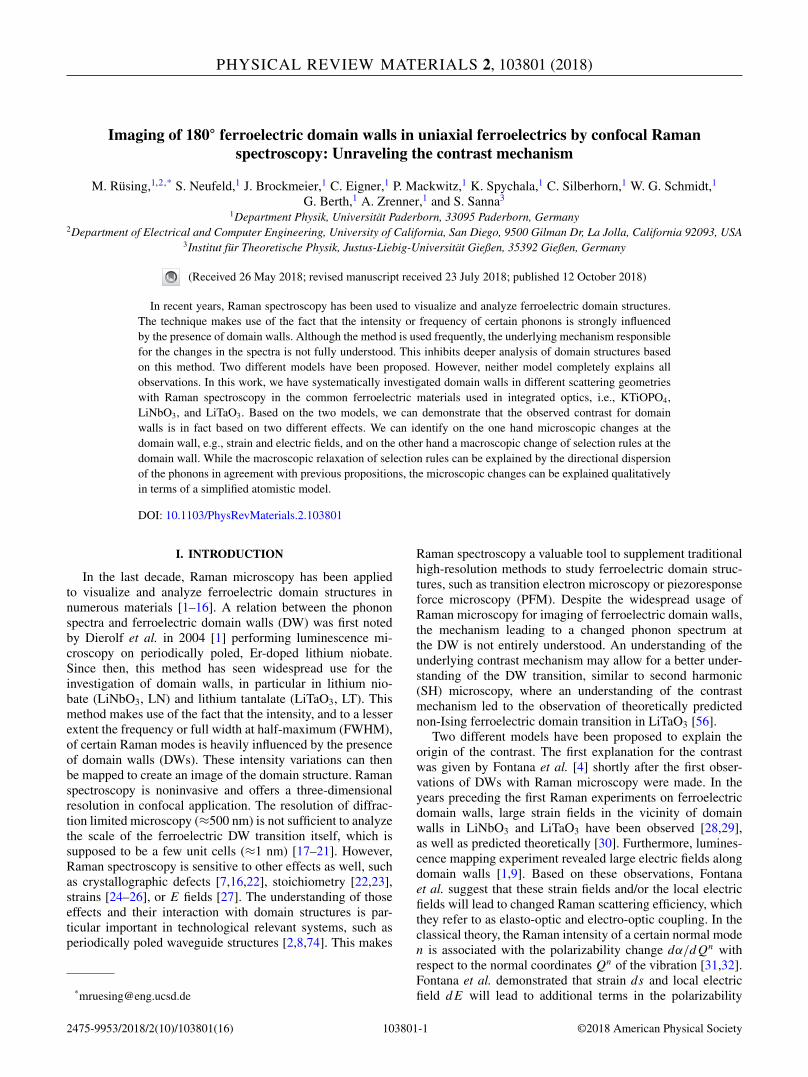
The measurements in this work are performed with acustom built confocal Raman setup shown in Fig. 2. For exci-tation we use a frequency-doubled Nd:YAG laser at 532 nm incontinuous wave operation with an output power up to 50 mW.The excitation beam is focused onto the sample via a infinitycorrected objective lens (Mitutoyo Plan Apo 100×; NA =0.7), which also collects the scattered light (backscattering
103801-2
IMAGING OF 180◦ FERROELECTRIC DOMAIN … PHYSICAL REVIEW MATERIALS 2, 103801 (2018)
100x / / 0.7
cw-Nd:YAG@532 nm
(b)
HWP
Analysator
Pinholemodule
Spektrograph
Telescope
Notchfilter
Line scan
100x / / 0.7
(a)
3D Pos
α
Goniometer
y x
z
FIG. 2. (a) Sketch of the sample geometry. Here, a typical linescan is highlighted. (b) Sketch of the Raman setup used for anal-ysis. For scanning, the samples are mounted to a piezodriven 3Dpositioner, which allows scanning with respect to a fixed focus. Tomeasure the directional dispersion the 3D positioner is exchangedfor a stepper motor with an attached sample mount.
operation). For depth discrimination, a confocal pinhole witha diameter of 10 μm is inserted in the detection path. Basedon the parameters of the pinhole and objective lens, this resultsin a spatial resolution of <500 nm in lateral and <2000 nmin axial direction in vacuum, which decreases, when focus-ing into a highly refracting material especially along theaxial direction [34]. However, this is of no concern for thisstudy as investigations will be performed parallel to the DWplanes. The spectral analysis is provided via a single-stagespectrometer with holographic grating and integrated notchfilter (KOSI Holospec f/1.8i) with an attached CCD camera(Andor Newton, BI). For Raman imaging, a scanning proce-dure is necessary. In our setup, scanning is performed withrespect to a fixed focus position. The samples are mountedon a piezostage (Piezosystem Jena Tritor), which offers a2-nm resolution. To measure angular-resolved spectra, thethree-dimensional (3D) positioner is substituted for a steppermotor with an attached sample mounting. The excitation anddetection polarizations can be controlled via a half-wave plate(HWP) and analyzer, respectively.
In this paper polarization-dependent Raman spectroscopywill be performed. To unambiguously identify the scatter-ing geometries the Porto notation [ki (ei, es )ks] will be used,where the vectors ki,s denote the direction of the incident andscattered light in crystal coordinates, while ei,s references thepolarization of the light with respect to the crystal axis system[8,23,35].
TABLE I. Observable phonon mode branches and Raman tensorelements for backscattering configurations. For more details on theselection rules in these materials, the respective specialized papersshould be referred [23,36–38].
LiTaO3 and LiNbO3 KTiOPO4
Scattering Tensor Phonon Tensor Phonongeometry elements branch elements branch
x(y, y )x a2 + c2 A1-TO + E-TO b2 A1-TOx(y, z)x d2 E-TO f 2 B2-TOx(z, z)x b2 A1-TO c2 A1-TOy(x, x )y a2 + c2 A1-TO + E-LO a2 A1-TOy(x, z)y d2 E-TO e2 B1-TOy(z, z)y b2 A1-TO c2 A1-TOz(x, x )z a2 + c2 A1-LO + E-TO a2 A1-LOz(x, y )z c2 E-TO d2 A2-TOz(y, y )z a2 + c2 A1-LO + E-TO b2 A1-LO
Taking the three main crystal axes into account, this meansthat nine different scattering geometries in backscattering,where ki = −ks , are possible. Depending on the scatteringconfiguration different symmetry species of phonon modesbelonging to different tensor elements will be detected. Forthe three analyzed materials, the resulting selection rules arelisted in Table I. For more details on the selection rules in thesematerials, the respective specialized papers should be referred[23,36–38].
B. Angular-resolved Raman spectroscopy
The contrast for domain walls in Raman microscopy isexplained by Stone and Dierolf by a relaxation of the selectionrules by treating the domain wall as a large, planar defect.Therefore, it is expected that phonons propagating at obliqueangles with respect to the wall will also participate in thescattering. In polar crystals, like LN, LT, or KTP, the phononspectrum will change as a function of the propagation angleof the phonons, which is called directional dispersion. Inthe theory of directional dispersion [33,39–43] two typesof phonons are distinguished. The first type are ordinaryphonons, which do not shift and vary in spectroscopy undervarious angles, and extraordinary phonons, which shift underangular observation. This is a prominent effect in polar ma-terials, such as ferroelectrics. This effect can be understoodas the coupling of phonons to long-range electric fields. Theterms “ordinary” and “extraordinary” are chosen in analogyto the ordinary and extraordinary optical axes. In particular,phonons propagating parallel to the extraordinary axis, theaxis of the internal field, are subject to changes. In contrast tothis, phonons in the ordinary plane are usually not subject tochange. It should be noted that KTP is a biaxial material withthree refractive indices. Hence, extraordinary phonons with apronounced directional dispersion are also expected in the xy
plane.To measure directional dispersions, the samples are
mounted on the goniometer stage and the sample was tiltedwith respect to the fixed focus axis. It should be noted thatthe outer tilt angle β does not represent the angle α at whichthe phonon is excited. Due to refraction the excitation angle is
103801-3
M. RÜSING et al. PHYSICAL REVIEW MATERIALS 2, 103801 (2018)
α
β
zx
y
β
( (
(c) (d)
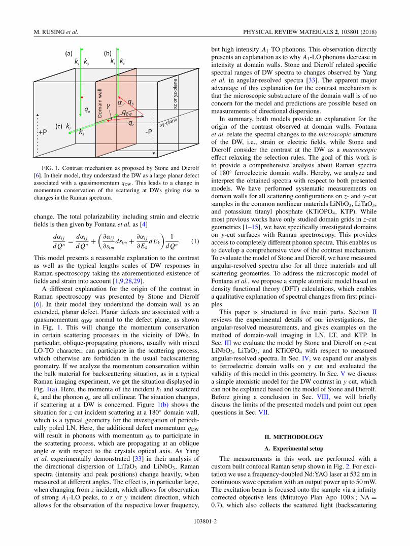
FIG. 3. (a), (b) Show the angular-dependent Raman spectra of KTP and LT. The crystal is tilted in steps of 5◦ along the y axis as shownin the inset. The light polarization is kept fixed according to the 0◦ scattering geometry z(x, x )z. Spectra of DWs for KTP and LN have beenmeasured [(c) and (d)]. Several modes, which show a pronounced angular-dependent behavior [(a) and (b)], also show a sensitivity for domainwalls [(c) and (d)].
changed according to the inset in Fig. 3. The angles have beencorrected by using Snell’s law
nair sin(β ) = nmaterial sin(α). (2)
Lithium niobate has an extraordinary refractive index at532 nm of approximately n = 2.23. This means that thesample needs to be tilted by 47◦ to record the spectrum atα = 20◦. Alike, the corrections have been performed for KTPand LT.
Figures 3(a) and 3(b) show a series of Raman spectra takenevery 5◦ of tilting. Due to internal reflection only spectra upto approximately 25◦ in LN and LT and 30◦ in KTP couldbe taken. The light polarization in the experimental setupwas kept fixed according to the starting scattering geometry,which in this case was z(x, x)z in Porto notation. The spectraare normalized to maximum after the dark counts has beensubtracted. For better visibility, they are separated by 0.5. Thisenables to compare the relative changes in the directional-dependent spectra with the features of the DW spectrum. Foran easier comparison, some spectral features have been high-lighted. The modes in LiNbO3 and LiTaO3 are labeled withrespect to the commonly accepted assignments [23,35,38,44].
For KTiOPO4, no generally accepted assignment is available,therefore, the approximate mode wave numbers are given.
C. Raman imaging and samples
Three samples have been analyzed. The periodically poledlithium niobate and lithium tantalate samples have been com-mercially obtained from Deltronic Crystals, Inc. The lithiumniobate crystal features a period length of � = 28.3 μm anda duty cycle of 60:40, while the lithium tantalate crystalis poled with a period length of � = 28.9 μm with a dutycycle of 50:50. Both samples are fabricated from congruentmaterial. To enable the optical analysis, both samples havebeen polished on one z face and one y face, respectively. Here,the polishing step also makes sure that any etching pattern isremoved.
The KTP sample was fabricated in the in-house technology[8,45] in Paderborn. At first, a commercial flux grown KTPwafer is cut into pieces with dimensions of about 10 (x) by6 (y) by 1 (z) mm3. The samples are immersed in a pureKNO3 melt to homogenize the potassium stoichiometry. Ina photolithographic patterning step, a periodic photo resiststructure is fabricated on the z face of the crystals. Both sides
103801-4
IMAGING OF 180◦ FERROELECTRIC DOMAIN … PHYSICAL REVIEW MATERIALS 2, 103801 (2018)
FIG. 4. Raman imaging is demonstrated for LiNbO3, LiTaO3, and KTiOPO4 samples. Each image is created using the integrated intensityin a specified spectral range of the Raman spectrum, which was chosen based on previous works [2,4,8,10,14]. The graph below each imagegives a cross section along the red dashed line. Here, domain-wall signatures down to 600 nm can be observed, which is limited by opticalresolution, while the domain transition may be much smaller. The Raman spectra were taken in z(x, x )z scattering geometry.
are electrically contacted and several high voltage pulses areapplied to the sample to periodically pole the crystal. Thepoling progress is monitored with an in situ optical monitoringbased on the electro-optic effect [46]. The domain structurefeatures a poling period of � = 7.6 μm and a duty cycleof approximately 50:50. Alike, the KTP sample has beenpolished on the z face and one y face for optical analysis. Allsamples have domain walls oriented parallel to the the y axisaccording to Fig. 2.
Figure 4 shows ferroelectric domain structures revealedby Raman imaging on all three samples. The images on theLiNbO3 and LiTaO3 samples show a 50 × 30 μm2 (x × y)surface with visible DWs, while the KTiOPO4 shows a smallerregion of 25 × 30 μm2 (x × y). For the scans, the focus wasplaced typically 5 to 10 μm below the sample surface, toensure that no surface phonon spectrum will interfere withthe measurements [47]. For each material spectral rangesare known, which show a systematic decrease or increasein intensity. A straightforward and convenient method togenerate images of domain wall is to integrate the intensityin such a spectral range [10]. This integrated intensity is thenplotted with respect to the spatial coordinates of the measuredspectrum to reveal the domain structure. For our images, wechose material-specific spectral ranges, which are known toprovide an increased signal at DWs. In detail, we chose therange from 570 to 610 cm−1 for LT [10], the region from 560–630 cm−1 in LN [2,4,14], and the region of 560–630 cm−1 forKTP [8].
The results are shown in Figs. 4(a)–4(c). Here, the periodlength differences as well as the different duty cycles canbe seen. Below each image a plot of the intensity profilesalong the red dashed line is given. In this experiment, wedetect DW signatures [full width at half-maxima (FWHM)]down to 600 nm. This is mainly moderated by the reso-lution limit of optical microscopy and not by the size ofthe domain wall, which is likely to be significantly smallerthan this. Here, other methods, e.g., PFM, reveal domaintransitions down to be 20–80 nm for LN or KTP [48] or
even less [17–19]. The observed signatures are well com-parable to typical Raman signatures of DWs [1–15] andtherefore are typical candidates for the analysis of the contrastmechanism.
III. DW SPECTRA IN z INCIDENT
Based on the imaging procedure discussed in the previoussection individual domain walls are located and Raman spec-tra are measured. In Figs. 3(c) and 3(d), two examples for aDW spectrum for KTiOPO4 and LiTaO3 are shown. Here, theDW spectrum is given in dashed green lines. For comparison,a bulk reference spectrum is also shown. Both spectra areshown as measured and are not normalized. The comparisonreveals shifts and intensity variations in several modes, but noadditional lines. This observation is consistent with literature[6,8]. To better highlight the differences, it is convenientto plot the difference spectrum. Here, the bulk spectrum issubtracted from the DW spectrum [I (DW) − I (bulk)] andplotted below in red. The macroscopic model by Stone andDierolf associates the spectra of oblique propagating phononswith the DW spectrum. Indeed, in a direct comparison manyfeatures of the domain-wall spectrum can be connected toangular-dependent changes [Figs. 3(a) and 3(b)].
For a systematic analysis, DW spectra and bulk spectrahave been taken in all three independent scattering config-urations [z(x, x)z, z(x, y)z, and z(y, y)z]. The differencespectra have been calculated and plotted in the top panelsin Figs. 5(a)–5(i). For reference the bulk spectrum in therespective geometry was added. The plots reveal DW relatedchanges in all scattering configurations. In LN and LT, thez(x, x)z and z(y, y)z DW spectra are similar changes. Thiscan be understood because both spectra will address the sameRaman tensor element [23,35], as well as due to geometricreasons similar angular-dependent changes are expected. ForKTP the situation is slightly different because the z(x, x)z andz(y, y)z spectra will show the same branch of A1 phonons,but related to a different tensor element (compare Table I).
103801-5
M. RÜSING et al. PHYSICAL REVIEW MATERIALS 2, 103801 (2018)
(e) z(x,y)z (h) z(x,y)z
(d) z(x,x)zLiNbO3
(i) z(y,y)z(f) z(y,y)z
LiTaO3 KTiOPO4(a) z(x,x)z
(b) z(x,y)z
(c) z(y,y)z
(g) z(x,x)z
FIG. 5. The figure shows the spectral signatures of domain walls on z incident for all three materials in the top panels. Here, in black abulk spectrum is given for reference, while the red line denotes the difference spectrum calculated from the measured DW spectrum [I (DW) −I (bulk)]. Below are the 0◦ and 25◦ angular-resolved spectra, where 0◦ is equal to the bulk spectrum in the top panel. To highlight differences,also a difference spectrum is given [I (25◦) − I (0◦)].
103801-6
IMAGING OF 180◦ FERROELECTRIC DOMAIN … PHYSICAL REVIEW MATERIALS 2, 103801 (2018)
Nevertheless, the DW spectrum for both geometries showssimilar changes, in particular, the red-shift and decrease of themost intense line at 765 cm−1.
The goal is now to systematically compare domain-wallspectra and angular-resolved spectra in z incident. Fig-ures 3(a) and 3(b) demonstrate that the spectral changeswith respects to angle are continuous, which is consistentwith literature [33]. Therefore, to identify the largest changescaused by angular dispersion it may be enough to comparetwo spectra, a 0◦ (bulk) spectrum and a 25◦ spectrum, whichis the largest angle, which can be measured for all samples.Due to increased reflection at higher angles and changingscattering efficiencies, the spectra have been normalized sim-ilar to Figs. 3(a) and 3(b). These 0◦ (black) and 25◦ (green)spectra are plotted in the bottom panels in Figs. 5(a)–5(i).For a convenient comparison, a difference spectrum (red)between the 0◦ (black) and 25◦ (green) has been calcu-lated similar to the method for the DW difference spectrum[I (25◦) − I (0◦)].
Although this difference spectrum is calculated from nor-malized spectra, the accordances between the DW differ-ence spectra and angular-resolved difference spectra are sur-prisingly large. Many of the observed features of the DWspectrum can be readily explained in this comparison. Forexample, in previous works it was observed that so-calledA1-LO [6,8,35] usually show a decrease in intensity at DWs.While other spectral ranges, where in x- or y-incident geome-tries extremely intense phonons are observed, e.g., A1-TO,an increase of intensity is seen in the DW spectrum as well.Both of these observations can be readily understood basedon the theory of directional dispersion. Pure A1-LO phononsin polar crystals can only be observed in scattering configura-tions along the axis of the spontaneous polarization, whichis the z direction. These phonons will gradually shift anddisappear by tilting to any other crystal direction [33,39–43].In contrast to this, pure so-called A1-TO phonons can onlybe observed in geometries orthogonal to the z axis, i.e.,the extraordinary plane. Therefore, these spectral rangeswill increase in intensity at the DW. This, for example,
explains the strong increase in LN at 620 cm−1 and at580 cm−1 in LT, which is consistent with previous suggestions[6,23].
For the z(x, y)z geometries in LN and LT the predictions[z(x, y)z] are less conclusive. This is, however, expected asthese geometries show so-called E-TO modes (see Table I).The E modes for LN and LT have no pronounced directionalshifts, as the E-TO modes are ordinary modes and appear atthe same frequencies after the respective full turn. Neverthe-less, some contrast for the DW can be seen. This may be, atleast partially, by the fact that the scattering efficiency willchange as a different Raman tensor element will be addressed[35,44]. However, as we will see below, other effects may bepresent.
So far, we have shown that the model by Stone andDierolf can sufficiently enough explain the changes observedat domain walls in z-incident geometry. Further, we havedemonstrated that the analysis of angular-resolved spectraallows to predict the contrast behavior. The next questionis if this model also provides reliable predictions for y-cutscattering configuration.
IV. DW SPECTRA IN y INCIDENT
To analyze DW spectra at y-incident geometry, locationsof domain walls need to be identified. Most Raman investiga-tions were performed in z incident though [1–16]. Therefore,domain-structure-sensitive phonons have to be identified first.To be able to also detect any subtle changes in the spectrum,we have fitted selected lines with a Lorentzian function of theform
I (ω) = A
2π
δ(ω2 − ω2
c
) + δ2/4, (3)
where the prefactor A gives the integrated intensity of the line,ωc is the resonance or peak frequency, and δ specifies theFWHM of the line. This allows to investigate the changes ofline shifts, intensities, and FWHMs. Figure 6 shows the resultof such an investigation of a line scan of 100 μm on LiNbO3.While the intensity A only shows a weak connection to the
FIG. 6. (a) Raman spectrum taken in y(z, z)y scattering geometry for LiNbO3. The A-TO4 line has been fitted with a Lorentzian function.The inset demonstrates the measurement geometry, in which y-cut domains have been investigated. (b) Fitting results of a line scan on theLiNbO3. The domain walls are associated with a clear shift of the peak frequency, while in the intensity only a light imprint can be seen.
103801-7
M. RÜSING et al. PHYSICAL REVIEW MATERIALS 2, 103801 (2018)
(c) y(x,x)y - A-TO4
(d) y(x,z)y - E-TO1
LiNbO3
(b) y(x,z)y - E-TO1
LiTaO3 KTiOPO4
(a) y(x,x)y - A-TO4 (e) y(x,x)y - 691 cm-1
(f) y(x,z)y - 783 cm-1
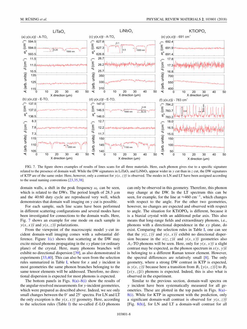
FIG. 7. The figure shows examples of results of lines scans for all three materials. Here, each phonon gives rise to a specific signaturerelated to the presence of domain wall. While the DW signatures in LiTaO3 and LiNbO3 appear wider in y cut than in z cut, the DW signaturesof KTP are of the same order. Here, however, only a contrast for y(x, z)y is observed. The modes in LN and LT have been assigned accordingto the usual naming conventions [23,35,38].
domain walls, a shift in the peak frequency ωc can be seen,which is related to the DWs. The period length of 28.3 μmand the 40:60 duty cycle are reproduced very well, whichdemonstrates that domain wall imaging on y cut is possible.
For each sample, such line scans have been performedin different scattering configurations and several modes havebeen investigated for connections to the domain walls. Here,Fig. 7 shows an example for one mode on each sample iny(x, x)y and y(x, z)y polarizations.
From the viewpoint of the macroscopic model y-cut in-cident domain-wall imaging comes with a substantial dif-ference. Figure 1(c) shows that scattering at the DW mayexcite mixed phonons propagating in the xy plane (or ordinaryplane) of the crystal. Here, many phonons branches willexhibit no directional dispersion [39], as also demonstrated inexperiments [33,40]. This can also be seen from the selectionrules summarized in Table I, where for x and y incident inmost geometries the same phonon branches belonging to thesame tensor elements will be addressed. Therefore, no direc-tional dispersion is expected for most phonons is expected.
The bottom panels in Figs. 8(a)–8(i) show the results ofthe angular-resolved measurements for y-incident geometries,which were prepared as described above. Indeed, we see onlysmall changes between the 0◦ and 25◦ spectra. For LN and LTthe only exception is the y(x, x)y geometry. Here, accordingto the selection rules (Table I) the so-called E-LO phonons
can only be observed in this geometry. Therefore, this phononmay change at the DW. In the LT spectrum this can beseen, for example, for the line at ≈460 cm−1, which changeswith respect to the angle. For the other two geometries,however, no changes are expected and observed with respectto angle. The situation for KTiOPO4 is different, because itis a biaxial crystal with an additional polar axis. This alsomeans that long-range fields and extraordinary phonons, i.e.,phonons with a directional dependence in the xy plane, doexist. Comparing the selection rules in Table I, one can seethat the y(z, z)y and y(x, x)y exhibit no directional disper-sion because in the x(z, z)x and y(x, x)y geometries alsoA1-TO phonons will be seen. Here, only for y(x, x)y a slightcontrast may be expected, as the phonon spectrum in x(y, y)xis belonging to a different Raman tensor element. However,the spectral differences are relatively small [8]. The onlygeometry, where a strong DW contrast in KTP is expected,is y(x, z)y because here a transition from B1 [y(x, z)y] to B2
[x(y, z]x) phonons is expected. Indeed, this is also what isobserved in the experiment.
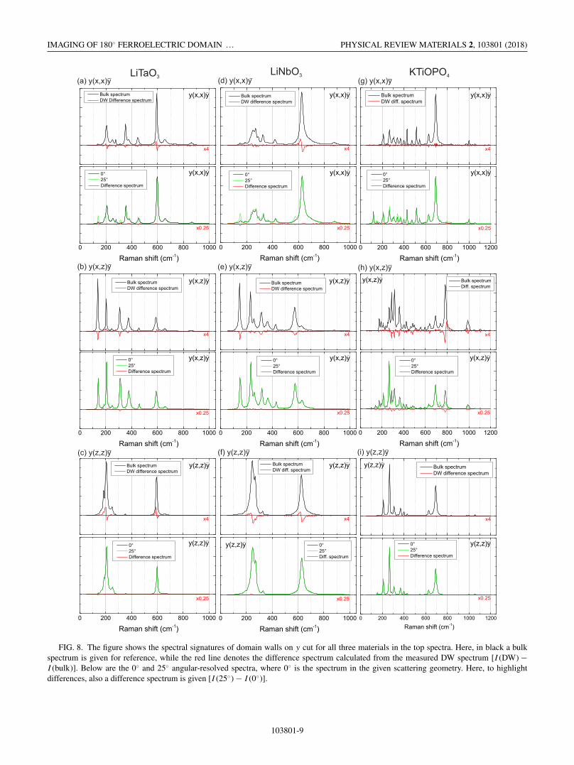
Similar to the previous section, domain-wall spectra ony incident have been systematically measured for all ge-ometries. These are plotted in the top panels in Figs. 8(a)–8(i). While for KTP in agreement with the prediction, onlya significant domain-wall contrast is observed for y(x, z)y[Fig. 8(h)], for LN and LT a domain-wall contrast for all
103801-8
IMAGING OF 180◦ FERROELECTRIC DOMAIN … PHYSICAL REVIEW MATERIALS 2, 103801 (2018)
(e) y(x,z)y (h) y(x,z)y
(i) y(z,z)y(f) y(z,z)y(c) y(z,z)y
(d) y(x,x)yLiNbO3LiTaO3 KTiOPO4
(a) y(x,x)y (g) y(x,x)y
(b) y(x,z)y
FIG. 8. The figure shows the spectral signatures of domain walls on y cut for all three materials in the top spectra. Here, in black a bulkspectrum is given for reference, while the red line denotes the difference spectrum calculated from the measured DW spectrum [I (DW) −I (bulk)]. Below are the 0◦ and 25◦ angular-resolved spectra, where 0◦ is the spectrum in the given scattering geometry. Here, to highlightdifferences, also a difference spectrum is given [I (25◦) − I (0◦)].
103801-9
M. RÜSING et al. PHYSICAL REVIEW MATERIALS 2, 103801 (2018)
geometries is seen. For example, the most dominant peak inthe y(x, z)y geometry for LT [Fig. 8(h)] at about 590 cm−1
shows a large shift towards lower frequencies. This is in strongcontrast to the observation from the directional dispersion.The predictions based on the directional dispersion reproducethe changes of the E-LO modes well, which is, for example,seen in the behavior of the ≈460 cm−1 line. Even morestriking are the differences for the y(z, z)y spectra for LT andLN, where no contrast at all was expected, and yet intensitychanges and shifts are observed [Figs. 8(c) and 8(f)], whichalso lead to high-contrast images as shown in Figs. 7 and 6.
It appears that the macroscopic model based on the di-rectional dispersions can only explain the DW contrast inKTP and the behavior of the E-LO in LN and LT [y(x, x)y],while the major changes in the LN and LT spectra remain notexplained. To explain this behavior, we take a look at the linescans of DWs presented in Fig. 7.
While the signatures of the domain walls for KTiOPO4
show a similar width of 600 nm in y cut as in z cut, we observefor LiNbO3 and LiTaO3 signatures with half-widths between1000 and 2000 nm in Figs. 8 and 6. This is significantly largerthan the results observed in z cut in the Sec. II (Fig. 4). Itshould be stressed again at this point that the results for z
cut and y cut both have been obtained on the same samplesand with the same experimental setup. The only difference isthe scattering geometry. This suggests that we have a differ-ent, physical mechanism (with longer influence range) beingresponsible for the spectral changes than the macroscopicrelaxation of selection rules. And this mechanism is, at leastin this experiment, only present in LiNbO3 and LiTaO3, butnot in KTiOPO4. The explanation may be the aforementionedstrain and/or electric fields in agreement with the suggestionof Fontana et al. [4].
Indeed, in particular in congruent LiNbO3 and LiTaO3 amultitude of effects have been observed in the vicinity ofdomain walls. Strain fields in the order of 10 μm have beenobserved by x-ray topography spanning around domain walls[28,29]. As LiNbO3 and LiTaO3 are piezoelectric, this strainwill likely be associated with an electric field. Indeed, electricfields are present in the region of domain walls in congru-ent lithium niobate, as demonstrated by Dierolf et al. withluminescence microscopy [7,49]. Here, they detected fieldsbetween 4 and 6 kV/mm in a 4 to 10 μm range around thedomain wall. These strains and electric fields are on the samelength scale as changes in birefringence and refractive index,which have been observed in scales from 3 to 20 μm arounddomain walls in LN and LT [7,50,51]. In this context, Gopalanet al. pointed out different response length scales for differentanalysis methods of domain walls, in agreement with ourobservation they detected DW signature width of 1.5 μm withRaman spectroscopy [7]. Why is no such behavior observedfor KTiOPO4 in our experiment? Here, the reason may lie inthe specific material properties of KTiOPO4, which is knownfor its very high ionic conductivity [52]. If any strains orelectric fields are present in KTiOPO4, they will be soonmasked by a charge rearrangement. This may also be thereason why domain-wall signatures are often reported to besmaller in KTP compared to LN or LT [48].
The presence of electric fields and their influence on theRaman spectrum in lithium niobate allows to understand an-
other observation in the y-scan domain walls. In the line scansof lithium niobate in Figs. 7(c), 7(d), and 6 one can see in thepeak frequencies of the respective modes, do not only showa contrast for the domain wall, but apparently also a differentlevel between domains of a different polarity. Here, for theA1-TO phonon a difference of �ωc = 0.1 cm−1 is seen, whilefor the E-TO1 phonon a shift of �ωc = 0.05 cm−1 is detected.This can be explained based on the result of Stone et al., whoanalyzed the z-cut Raman spectrum of stoichiometric and con-gruent lithium niobate under applied electric fields orientedparallel to the z axis before and after domain inversion [27].They detected for all of their analyzed phonons a linear shiftof the mode frequency with respect to the applied electricfield, as well as a frequency difference between domains ofdifferent orientations. Depending on the phonon they detecteddifferences �ωc between 0.24 and 0.64 cm−1 of the peakfrequencies of phonon between domains of different polarity.
According to Stone et al., the proportionality constantsbetween frequency shift and electric field βE have valuesbetween 0.01 to 0.03 cm−1mm/kV for most modes. Unfor-tunately, they did not provide data for A1-TO4 from y cutbecause they measured from z cut, which only shows A1-LOmodes. However, a βE between 0.01 to 0.03 cm−1mm/kVwill correspond to an internal field of 3–10 kV/mm basedon the A1-TO4 of �ωc = 0.1 cm−1, which is a reasonablemagnitude for the internal fields reported for congruent ma-terial [49,53–55]. Taking their proportionality constant forthe E-TO1 and assuming it can also be applied in y-cutspectra, we obtain an internal electric field of 2 kV/mm withβE = 0.024 cm−1mm/kV and �ωc = 0.05 cm−1. A differentabsolute field strength determined by different phonons mayalso suggest off-axis E-field or strain components, as theE-TO1 has a displacement pattern mainly in the xy planein contrast to the A1-TO4, which has has a total-symmetricdisplacement pattern conserving the symmetry along the z
axis [23].
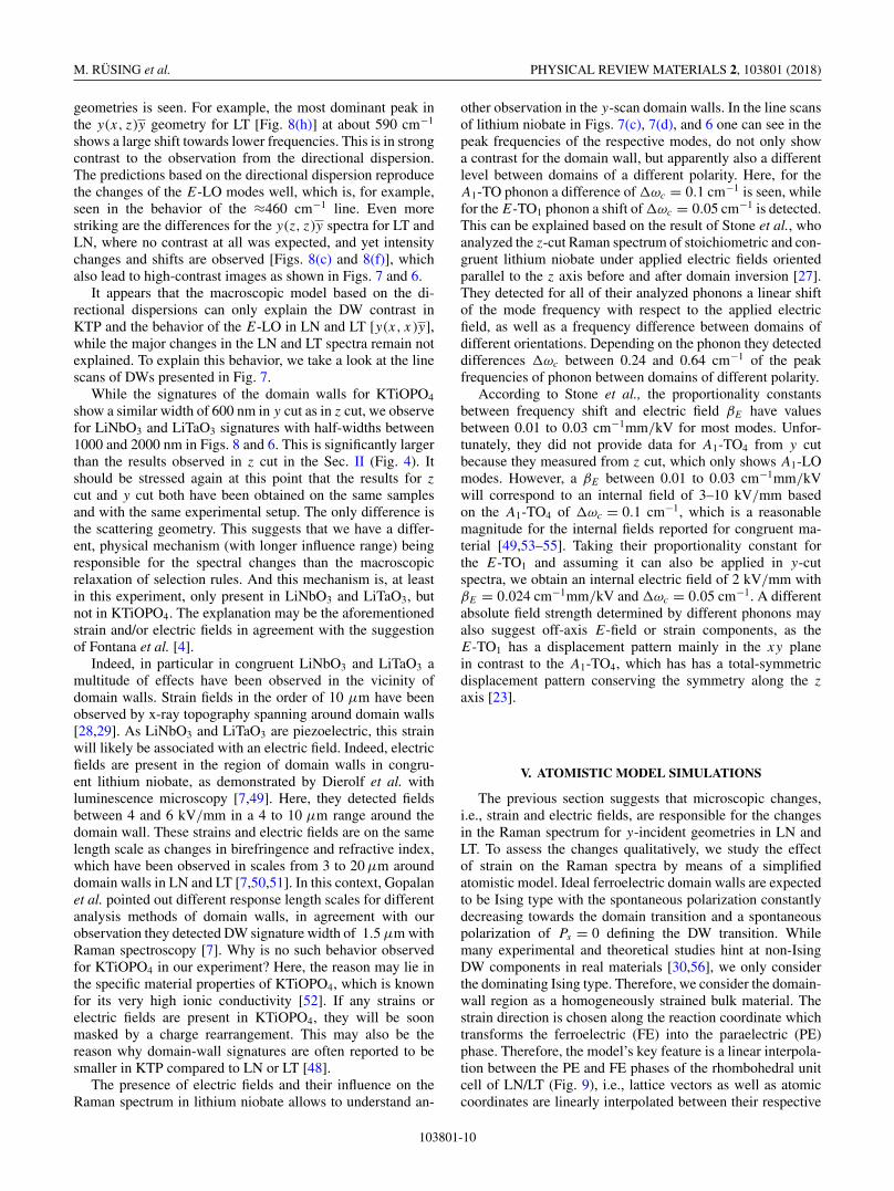
V. ATOMISTIC MODEL SIMULATIONS
The previous section suggests that microscopic changes,i.e., strain and electric fields, are responsible for the changesin the Raman spectrum for y-incident geometries in LN andLT. To assess the changes qualitatively, we study the effectof strain on the Raman spectra by means of a simplifiedatomistic model. Ideal ferroelectric domain walls are expectedto be Ising type with the spontaneous polarization constantlydecreasing towards the domain transition and a spontaneouspolarization of Ps = 0 defining the DW transition. Whilemany experimental and theoretical studies hint at non-IsingDW components in real materials [30,56], we only considerthe dominating Ising type. Therefore, we consider the domain-wall region as a homogeneously strained bulk material. Thestrain direction is chosen along the reaction coordinate whichtransforms the ferroelectric (FE) into the paraelectric (PE)phase. Therefore, the model’s key feature is a linear interpola-tion between the PE and FE phases of the rhombohedral unitcell of LN/LT (Fig. 9), i.e., lattice vectors as well as atomiccoordinates are linearly interpolated between their respective
103801-10
IMAGING OF 180◦ FERROELECTRIC DOMAIN … PHYSICAL REVIEW MATERIALS 2, 103801 (2018)
FIG. 9. Rhombohedral unit cell of LN/LT for different statesalong the reaction coordinate ξ between the ferroelectric (ξ = 1)and paraelectric phase (ξ = 0). O atoms are indicated in red, whilewhite and black circles represent Nb/Ta and Li, respectively. Note thedisplacement � zO between the oxygen octahedron and the centralniobium along the ferroelectric z axis as well as the displacement� zLi of the lithium sublattice. Rhombohedral lattice constants ϕ anda are indicated.
PE and FE values:
�a(ξ ) = ξ · �aFE + (1 − ξ ) · �aPE (4)
with 0 � ξ � 1. This interpolation accounts for the changeof internal polarization assuming an ideal Ising-type alongthe z axis, as well as strain effects along/perpendicular to z.The vicinity of the domain wall is therefore approximatelymodeled by domains with varying reaction coordinates ξ
along the paraelectric-ferroelectric reaction pathway, withthe domain-wall center being approximated to be in a pureparaelectric (ξ = 0) and the bulk material to be in a pure ferro-electric phase (ξ = 1). Density functional theory ground-statecalculations have then been performed within the generalizedgradient approximation (GGA) as parametrized by Perdew,Burke, and Ernzerhof (PBE) [57,58] and implemented in theVienna ab initio simulation package (VASP) [59,60]. The wavefunctions were expanded in plane waves up to a cutoff energyof 600 eV, while the integration over the Brillouin zone hasbeen carried out using a 5 × 5 × 5 k-point mesh. Atomic po-sitions and lattice vectors were relaxed until the total force act-ing on the system fell below a threshold value of 0.01 eV/Å.The resulting rhombohedral lattice constants of LN/LT withinthe ferroelectric and paraelectric phases are compiled inTable II. Phonon eigenvectors and differential Raman scat-tering efficiencies have been calculated via finite-differenceroutines. For numerical details we refer to Ref. [35]. Inthat work it has been shown that our DFT approach wellreproduces the measured bulk Raman data of LN and LT.Due to the neglect of long-range electric fields accompanyingLO phonon modes, our theoretical phonon spectra are limitedto TO phonons, which however is no strong limitation toreproduce effects in y-cut spectra, where only the weak E-LOmodes are present.
Since the changes of strain and internal polarization inthe vicinity of a domain wall are considered to be relatively
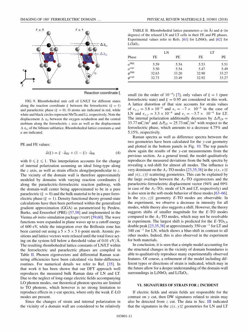
TABLE II. Rhombohedral lattice parameters a (in Å) and φ (indegrees) of the relaxed LN and LT cells in their FE and PE phases.Experimental values refer to Refs. [61] for LiNbO3 and [62] forLiTaO3.
LN LTPhase FE PE FE PE
aPBE 5.59 5.54 5.53 5.51aexpt 5.50 5.54 5.47 5.49φPBE 32.63 33.20 32.90 33.27φexpt 32.73 33.49 32.92 33.27
small (in the order of 10−4) [7], only values of ξ = 1 (pureferroelectric state) and ξ = 0.95 are considered in this work.A lattice distortion of that size accounts for strain valuesof εx,y = 3.8 × 10⁻⁴ and εz = −7 × 10⁻⁴ in the case ofLN and εx,y = 3.3 × 10⁻⁴ and εz = −3.7 × 10⁻⁴ for LT.The internal polarization additionally decreases by �PLN =33.77 mC/m2 and �PLT = 25.73 mC/m2 with respect to theferroelectric phase, which amounts to a decrease 4.75% and5.15%, respectively.
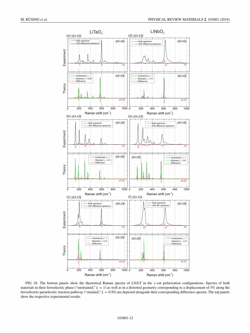
Raman spectra as well as difference spectra between thetwo geometries have been calculated for the y-cut geometryand plotted in the bottom panels in Fig. 10. The top panelsshow again the results of the y-cut measurements from theprevious section. As a general trend, the model qualitativelyreproduces the measured deviations from the bulk spectra byrevealing a red-shift for almost all modes. The influence isvery dominant on the A1-TO modes [23,35,38] in the y(x, x)yand y(z, z)y scattering geometries. This can be explained bythe large overlaps between the A1-TO eigenvectors and theparaelectric-ferroelectric displacement vector (94% and 69%in case of the A1-TO1 mode of LN and LT, respectively) andis also seen in the soft-mode behavior of these modes [63–66].In the y(x, z)y geometry E-TO modes are observable. Inthe experiment, we observe a decrease in intensity for allmodes, while theory also suggests a shift. However, the theorysuggests shifts of smaller magnitude for the E-TO modescompared to the A1-TO modes, which may not be resolvablein experiment. The largest shift is predicted for the E-TO5/6
double peak [23,35,38] at approximately 350 cm−1 for LT and340 cm−1 for LN, which shows a blue-shift in contrast to allother modes. Indeed, this is also observed in the experimentfor both materials.
In conclusion, it is seen that a simple model accounting forthe structural changes in the vicinity of domain boundaries isable to qualitatively reproduce many experimentally observedfeatures. Of course, a refinement of the model including dif-ferent types or directions of strain is indicated, which may inthe future allow for a deeper understanding of the domain-wallsurroundings in LiNbO3 and LiTaO3.
VI. SIGNATURES OF STRAIN FOR z INCIDENT
If electric fields and strain fields are responsible for thecontrast on y cut, then DW signatures related to strain mayalso be detected from z cut. The data in Sec. III indicatedthat the signatures in the z(x, y)z geometries for LN and LT
103801-11
M. RÜSING et al. PHYSICAL REVIEW MATERIALS 2, 103801 (2018)
LiTaO3
(e) y(x,z)y(b) y(x,z)y
(f) y(z,z)y(c) y(z,z)y
(d) y(x,x)yLiNbO3
(a) y(x,x)y
Theo
ryE
xper
imen
tTh
eory
Exp
erim
ent
Theo
ryE
xper
imen
t
FIG. 10. The bottom panels show the theoretical Raman spectra of LN/LT in the y-cut polarization configurations. Spectra of bothmaterials in their ferroelectric phase (“unstrained,” ξ = 1) as well as in a distorted geometry corresponding to a displacement of 5% along theferroelectric-paraelectric reaction pathway (“strained,” ξ = 0.95) are depicted alongside their corresponding difference spectra. The top panelsshow the respective experimental results.
103801-12
IMAGING OF 180◦ FERROELECTRIC DOMAIN … PHYSICAL REVIEW MATERIALS 2, 103801 (2018)
(d) LN z(x,y)z - E-TO1
(b) LN z(y,y)z - E-TO1(a) LN z(y,y)z - E-TO8
(c) LN z(x,y)z - E-TO8
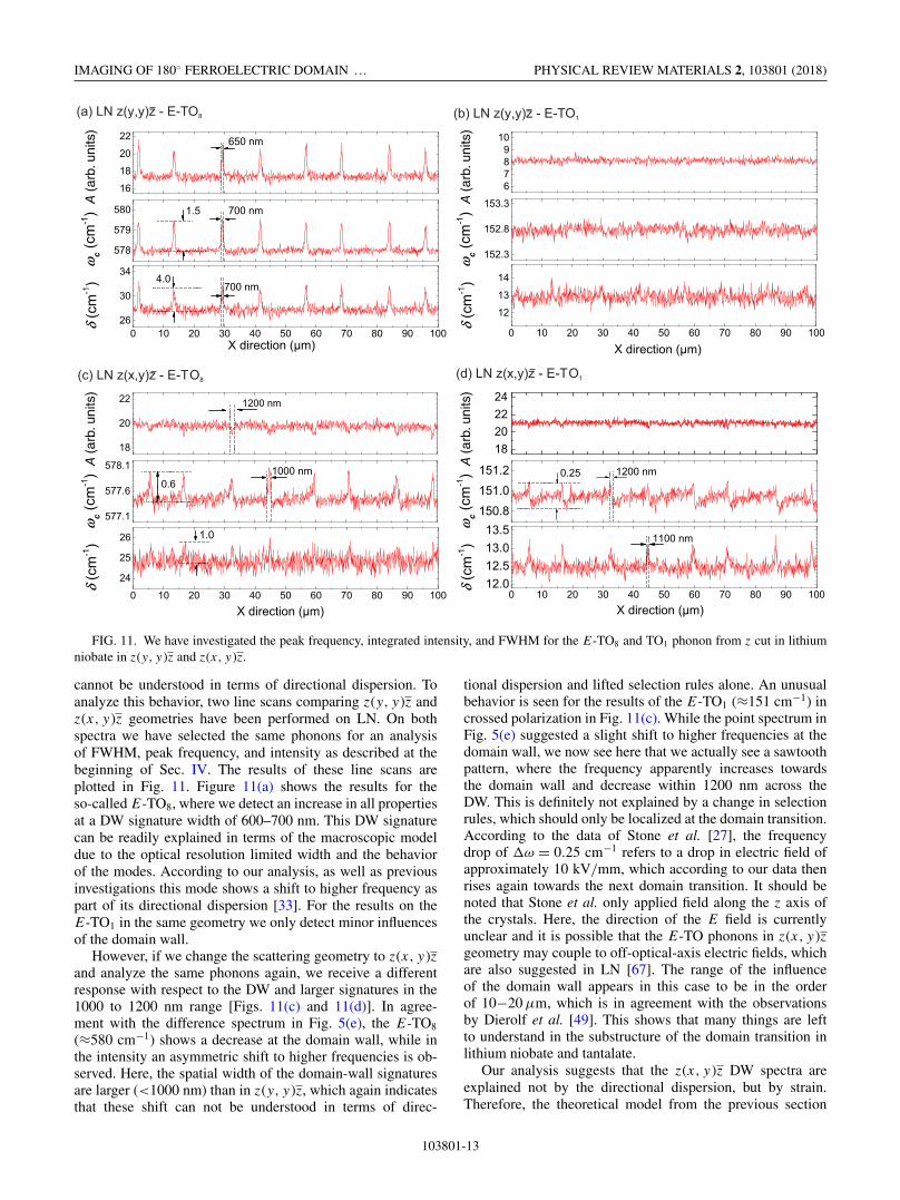
FIG. 11. We have investigated the peak frequency, integrated intensity, and FWHM for the E-TO8 and TO1 phonon from z cut in lithiumniobate in z(y, y )z and z(x, y )z.
cannot be understood in terms of directional dispersion. Toanalyze this behavior, two line scans comparing z(y, y)z andz(x, y)z geometries have been performed on LN. On bothspectra we have selected the same phonons for an analysisof FWHM, peak frequency, and intensity as described at thebeginning of Sec. IV. The results of these line scans areplotted in Fig. 11. Figure 11(a) shows the results for theso-called E-TO8, where we detect an increase in all propertiesat a DW signature width of 600–700 nm. This DW signaturecan be readily explained in terms of the macroscopic modeldue to the optical resolution limited width and the behaviorof the modes. According to our analysis, as well as previousinvestigations this mode shows a shift to higher frequency aspart of its directional dispersion [33]. For the results on theE-TO1 in the same geometry we only detect minor influencesof the domain wall.
However, if we change the scattering geometry to z(x, y)zand analyze the same phonons again, we receive a differentresponse with respect to the DW and larger signatures in the1000 to 1200 nm range [Figs. 11(c) and 11(d)]. In agree-ment with the difference spectrum in Fig. 5(e), the E-TO8
(≈580 cm−1) shows a decrease at the domain wall, while inthe intensity an asymmetric shift to higher frequencies is ob-served. Here, the spatial width of the domain-wall signaturesare larger (<1000 nm) than in z(y, y)z, which again indicatesthat these shift can not be understood in terms of direc-
tional dispersion and lifted selection rules alone. An unusualbehavior is seen for the results of the E-TO1 (≈151 cm−1) incrossed polarization in Fig. 11(c). While the point spectrum inFig. 5(e) suggested a slight shift to higher frequencies at thedomain wall, we now see here that we actually see a sawtoothpattern, where the frequency apparently increases towardsthe domain wall and decrease within 1200 nm across theDW. This is definitely not explained by a change in selectionrules, which should only be localized at the domain transition.According to the data of Stone et al. [27], the frequencydrop of �ω = 0.25 cm−1 refers to a drop in electric field ofapproximately 10 kV/mm, which according to our data thenrises again towards the next domain transition. It should benoted that Stone et al. only applied field along the z axis ofthe crystals. Here, the direction of the E field is currentlyunclear and it is possible that the E-TO phonons in z(x, y)zgeometry may couple to off-optical-axis electric fields, whichare also suggested in LN [67]. The range of the influenceof the domain wall appears in this case to be in the orderof 10−20 μm, which is in agreement with the observationsby Dierolf et al. [49]. This shows that many things are leftto understand in the substructure of the domain transition inlithium niobate and tantalate.
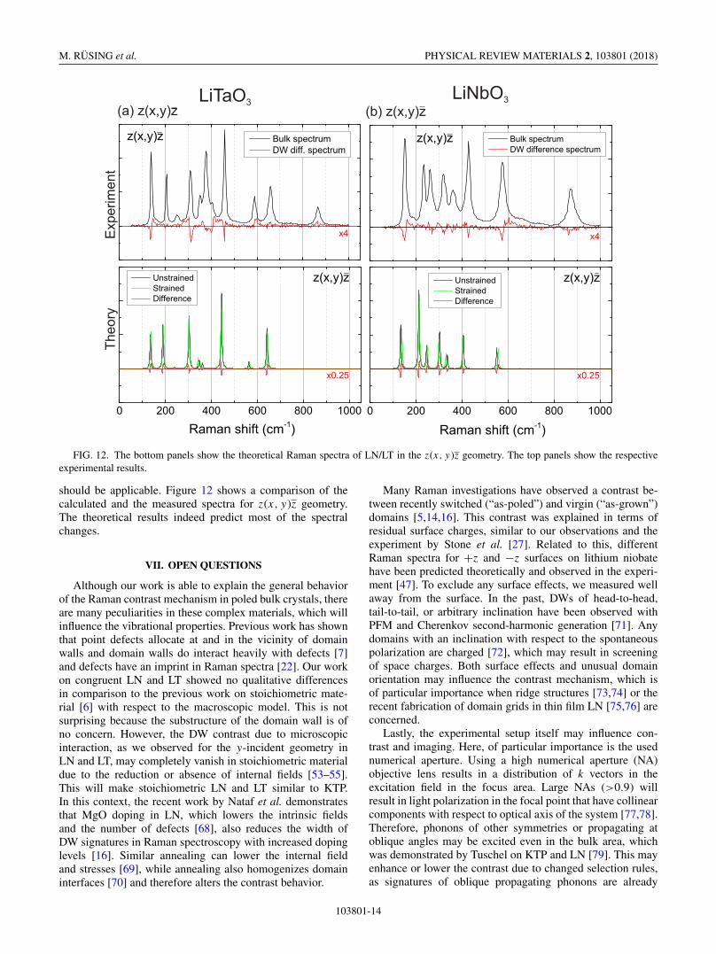
Our analysis suggests that the z(x, y)z DW spectra areexplained not by the directional dispersion, but by strain.Therefore, the theoretical model from the previous section
103801-13
M. RÜSING et al. PHYSICAL REVIEW MATERIALS 2, 103801 (2018)
LiNbO3(b) z(x,y)z
LiTaO3(a) z(x,y)z
Theo
ryE
xper
imen
t
FIG. 12. The bottom panels show the theoretical Raman spectra of LN/LT in the z(x, y )z geometry. The top panels show the respectiveexperimental results.
should be applicable. Figure 12 shows a comparison of thecalculated and the measured spectra for z(x, y)z geometry.The theoretical results indeed predict most of the spectralchanges.
VII. OPEN QUESTIONS
Although our work is able to explain the general behaviorof the Raman contrast mechanism in poled bulk crystals, thereare many peculiarities in these complex materials, which willinfluence the vibrational properties. Previous work has shownthat point defects allocate at and in the vicinity of domainwalls and domain walls do interact heavily with defects [7]and defects have an imprint in Raman spectra [22]. Our workon congruent LN and LT showed no qualitative differencesin comparison to the previous work on stoichiometric mate-rial [6] with respect to the macroscopic model. This is notsurprising because the substructure of the domain wall is ofno concern. However, the DW contrast due to microscopicinteraction, as we observed for the y-incident geometry inLN and LT, may completely vanish in stoichiometric materialdue to the reduction or absence of internal fields [53–55].This will make stoichiometric LN and LT similar to KTP.In this context, the recent work by Nataf et al. demonstratesthat MgO doping in LN, which lowers the intrinsic fieldsand the number of defects [68], also reduces the width ofDW signatures in Raman spectroscopy with increased dopinglevels [16]. Similar annealing can lower the internal fieldand stresses [69], while annealing also homogenizes domaininterfaces [70] and therefore alters the contrast behavior.
Many Raman investigations have observed a contrast be-tween recently switched (“as-poled”) and virgin (“as-grown”)domains [5,14,16]. This contrast was explained in terms ofresidual surface charges, similar to our observations and theexperiment by Stone et al. [27]. Related to this, differentRaman spectra for +z and −z surfaces on lithium niobatehave been predicted theoretically and observed in the experi-ment [47]. To exclude any surface effects, we measured wellaway from the surface. In the past, DWs of head-to-head,tail-to-tail, or arbitrary inclination have been observed withPFM and Cherenkov second-harmonic generation [71]. Anydomains with an inclination with respect to the spontaneouspolarization are charged [72], which may result in screeningof space charges. Both surface effects and unusual domainorientation may influence the contrast mechanism, which isof particular importance when ridge structures [73,74] or therecent fabrication of domain grids in thin film LN [75,76] areconcerned.
Lastly, the experimental setup itself may influence con-trast and imaging. Here, of particular importance is the usednumerical aperture. Using a high numerical aperture (NA)objective lens results in a distribution of k vectors in theexcitation field in the focus area. Large NAs (>0.9) willresult in light polarization in the focal point that have collinearcomponents with respect to optical axis of the system [77,78].Therefore, phonons of other symmetries or propagating atoblique angles may be excited even in the bulk area, whichwas demonstrated by Tuschel on KTP and LN [79]. This mayenhance or lower the contrast due to changed selection rules,as signatures of oblique propagating phonons are already
103801-14
IMAGING OF 180◦ FERROELECTRIC DOMAIN … PHYSICAL REVIEW MATERIALS 2, 103801 (2018)
present in the bulk spectra. Stone and Dierolf even used animmersion oil microscope providing a numerical aperture of1.32 for their system [6].
VIII. CONCLUSION
In this work, we have systematically performed Ramanspectroscopy on ferroelectric domain structures in LiNbO3,LiTaO3, and KTiOPO4 as well as atomistic calculations. Here,the goal was to obtain an extensive insight in the mechanism,which alters the Raman spectrum at domain walls and allowsfor visualization of domain structures. As seen in this work,we have been able to understand the contrast at domain wallsby a combination of a macroscopic model, which explains thecontrast in terms of relaxed selection rules, and a microscopicmodel, where local strain and electric fields modify the Ramanspectrum. Both effects appear not only to manifest in differentspectral responses, but also at different length scales. Theobservation of largely varying response lengths depending onthe method has been first pointed out by Gopalan et al. in2007 [7], where they noted that different analysis methodson domain walls in lithium niobate and tantalate yieldedlargely different width scales of domain walls. While theoryand direct observations of atomic displacements with electronmicroscopy methods showed the DW transition to be on theorder of a few unit cells [17–21], response length around
DWs up to the order of several 10 μm have been observedby Bragg topography (resolution a few microns) [28,29].Many other methods have demonstrated various responselength scales in-between, e.g., 1–80 nm with PFM (resolutiondown to nm; depending on tip radius) [48,80], 500–2000 nmwith luminescence, Raman and SHG microscopy (resolution<500 nm) [7,49,56,70,74] or refractive index analysis withnear-field scanning optical microscopy (NSOM) (resolution<100 nm) [50,51]. This work demonstrates this discrepancyto be present in one method, which can be explained in termsof two fundamentally different mechanisms. In the context ofthe microscopic model, we present a simple atomistic modelof strain and electric fields. While our simplified model is ableto reproduce the spectral modifications at the domain wall,it certainly does not fully capture the complexity of the realsystem. Nevertheless, this proposes a path to simulate andunderstand the domain-wall region on a microscopic scale inLN and LT and a way to close the gap between findings ofvarious response length around DWs [7].
ACKNOWLEDGMENTS
The authors acknowledge the Deutsche Forschungsge-meinschaft (DFG) for financial support by the SFB/TRR 142through Projects No. B04 and No. B05. The authors thank D.Kool for helpful discussions.
[1] V. Dierolf and C. Sandmann, Appl. Phys. B 78, 363 (2004).[2] G. Berth, W. Hahn, V. Wiedemeier, A. Zrenner, S. Sanna, and
W. G. Schmidt, Ferroelectrics 420, 44 (2011).[3] V. Y. Shur, P. S. Zelenovskiy, M. S. Nebogatikov, D. O. Alikin,
M. F. Sarmanova, A. V. Ievlev, E. A. Mingaliev, and D. K.Kuznetsov, J. Appl. Phys. 110 (2011).
[4] M. D. Fontana, R. Hammoum, P. Bourson, S. Margueron, andV. Y. Shur, Ferroelectrics 373, 26 (2008).
[5] P. Capek, G. Stone, V. Dierolf, C. Althouse, and V. Gopolan,Phys. Status Solidi C 4, 830 (2007).
[6] G. Stone and V. Dierolf, Opt. Lett. 37, 1032 (2012).[7] V. Gopalan, V. Dierolf, and D. A. Scrymgeour, Annu. Rev.
Mater. Res. 37, 449 (2007).[8] M. Rüsing, C. Eigner, P. Mackwitz, G. Berth, C. Silberhorn, and
A. Zrenner, J. Appl. Phys. 119, 044103 (2016).[9] Y. Zhang, L. Guilbert, and P. Bourson, Appl. Phys. B 78, 355
(2004).[10] V. Ya Shur and P. S. Zelenovskiy, J. Appl. Phys. 116, 066802
(2014).[11] V. Ya Shur, D. S. Chezganov, M. S. Nebogatikov, I. S. Baturin,
and M. M. Neradovskiy, J. Appl. Phys. 112, 104113 (2012).[12] P. S. Zelenovskiy, M. D. Fontana, V. Y. Shur, P. Bourson, and
D. K. Kuznetsov, Appl. Phys. A 99, 741 (2010).[13] R. Hammoum, M. D. Fontana, P. Bourson, and V. Y. Shur,
Ferroelectrics 352, 106 (2007).[14] R. Hammoum, M. Fontana, P. Bourson, and V. Shur, Appl.
Phys. A 91, 65 (2008).[15] Y. Kong, J. Xu, B. Li, S. Chen, Z. Huang, L. Zhang, S. Liu, W.
Yan, H. Liu, X. Xie, L. Shi, X. Li, and G. Zhang, Opt. Mater.27, 471 (2004).
[16] G. F. Nataf, M. Guennou, A. Haußmann, N. Barrett, and J.Kreisel, Phys. Status Solidi (RRL): Rapid Res. Lett. 10, 222(2016).
[17] C.-L. Jia, S.-B. Mi, K. Urban, I. Vrejoiu, M. Alexe, and D.Hesse, Nat. Mater. 7, 57 (2008).
[18] L. Bursill and P. J. Lin, Ultramicroscopy 18, 235 (1985).[19] Y. B. Chen, M. B. Katz, X. Q. Pan, R. R. Das, D. M. Kim, S. H.
Baek, and C. B. Eom, Appl. Phys. Lett. 90, 072907 (2007).[20] J. Padilla, W. Zhong, and D. Vanderbilt, Phys. Rev. B 53,
R5969(R) (1996).[21] B. Meyer and D. Vanderbilt, Phys. Rev. B 65, 104111 (2002).[22] M. D. Fontana and P. Bourson, Appl. Phys. Rev. 2, 040602
(2015).[23] M. Rüsing, S. Sanna, S. Neufeld, G. Berth, W. G. Schmidt,
A. Zrenner, H. Yu, Y. Wang, and H. Zhang, Phys. Rev. B 93,184305 (2016).
[24] M. R. Tejerina, D. Jaque, and G. A. Torchia, Opt. Mater. 36,936 (2014).
[25] M. R. Tejerina, K. Pereira da Silva, A. R. Goñi, and G. A.Torchia, Opt. Mater. 36, 581 (2013).
[26] M. R. Tejerina, D. Jaque, and G. A. Torchia, J. Appl. Phys. 112,123108 (2012).
[27] G. Stone, B. Knorr, V. Gopalan, and V. Dierolf, Phys. Rev. B84, 134303 (2011).
[28] T. Jach, S. Kim, V. Gopalan, S. Durbin, and D. Bright, Phys.Rev. B 69, 064113 (2004).
[29] K. Hassani, M. Sutton, M. Holt, Y. Zuo, and D. Plant, J. Appl.Phys. 104, 043515 (2008).
[30] D. A. Scrymgeour, V. Gopalan, A. Itagi, A. Saxena, and P. J.Swart, Phys. Rev. B 71, 184110 (2005).
103801-15
M. RÜSING et al. PHYSICAL REVIEW MATERIALS 2, 103801 (2018)
[31] W. Demtröder, New York (Springer, Berlin, 2007), Vol. 4, p. 726[32] H. Kuzmany, Solid-State Spectroscopy: An Introduction
(Springer, Berlin, 2009), pp. 1–554.[33] X. Yang, G. Lan, B. Li, and H. Wang, Phys. Status Solidi B 142,
287 (1987).[34] S. Hell, G. Reiner, C. Cremer, and E. H. K. Stelzer, J. Microsc.
169, 391 (1993).[35] S. Sanna, S. Neufeld, M. Rüsing, G. Berth, A. Zrenner, and
W. G. Schmidt, Phys. Rev. B 91, 224302 (2015).[36] M. Rüsing, T. Wecker, G. Berth, D. J. As, and A. Zrenner, Phys.
Status Solidi (b) 253, 778 (2016)[37] G. E. Kugel, F. Bréhat, B. Wyncket, M. D. Fontana, G. Marnier,
C. Carabatos-Nedelec, and J. Mangin, J. Phys. C: Solid StatePhys 21, 5565 (1988).
[38] S. Margueron, A. Bartasyte, A. M. Glazer, E. Simon, J. Hlinka,I. Gregora, and J. Gleize, J. Appl. Phys. 111, 104105 (2012).
[39] L. Merten, Phys. Status Solidi B 28, 111 (1968).[40] R. Claus, J. Brandmüller, G. Borstel, E. Wiesendanger, and L.
Steffan, Z. Naturforsch. A 27, 1187 (1972).[41] J. Onstott and G. Lucovsky, J. Phys. Chem. Solids 31, 2171
(1970).[42] N. Kuroda and Y. Nishina, Solid State Commun. 30, 95 (1979).[43] D. Olechna, J. Phys. Chem. Solids 31, 2755 (1970).[44] P. Hermet, M. Veithen, and P. Ghosez, J. Phys.: Condens. Matter
19, 456202 (2007).[45] V. Ansari, E. Roccia, M. Santandrea, M. Doostdar, C. Eigner,
L. Padberg, I. Gianani, M. Sbroscia, J. M. Donohue, L.Mancino, M. Barbieri, and C. Silberhorn, Opt. Express 26, 2764(2018).
[46] H. Karlsson and F. Laurell, Appl. Phys. Lett. 71, 3474 (1997).[47] S. Sanna, G. Berth, W. Hahn, A. Widhalm, A. Zrenner, and W.
G. Schmidt, Ferroelectrics 419, 1 (2011).[48] J. Wittborn, C. Canalias, K. V. Rao, R. Clemens, H. Karlsson,
and F. Laurell, Appl. Phys. Lett. 80, 1622 (2002).[49] V. Dierolf and C. Sandmann, J. Lumin. 125, 67 (2007).[50] S. Kim and V. Gopalan, Mater. Sci. Eng. B 120, 91 (2005).[51] T. J. Yang, V. Gopalan, P. J. Swart, and U. Mohideen, Phys. Rev.
Lett. 82, 4106 (1999).[52] N. I. Sorokina and V. I. Voronkova, Crystallogr. Rep. 52, 80
(2007).[53] Y.-L. Chen, J.-J. Xu, X.-Z. Zhang, Y.-F. Kong, X.-J. Chen, and
G.-Y. Zhang, Appl. Phys. A 74, 187 (2002).[54] A. Grisard, E. Lallier, K. Polgar, and A. Peter, Electron. Lett.
36, 1043 (2000).[55] K. Kitamura, Y. Furukawa, K. Niwa, V. Gopalan, and T. E.
Mitchell, Appl. Phys. Lett. 73, 3073 (1998).
[56] S. Cherifi-Hertel, H. Bulou, R. Hertel, G. Taupier, K. D. H.Dorkenoo, C. Andreas, J. Guyonnet, I. Gaponenko, K. Gallo,and P. Paruch, Nat. Commun. 8, 15768 (2017).
[57] J. P. Perdew, K. Burke, and M. Ernzerhof, Phys. Rev. Lett. 77,3865 (1996).
[58] M. Ernzerhof and G. E. Scuseria, J. Chem. Phys. 110, 5029(1999).
[59] G. Kresse and J. Furthmüller, Comput. Mater. Sci. 6, 15 (1996).[60] G. Kresse and J. Furthmüller, Phys. Rev. B 54, 11169 (1996).[61] H. Boysen and F. Altorfer, Acta Crystallogr., Sect. B 50, 405
(1994).[62] S. Abrahams, E. Buehler, W. Hamilton, and S. Laplaca, J. Phys.
Chem. Solids 34, 521 (1973).[63] J. Servoin and F. Gervais, Solid State Commun. 31, 387 (1979).[64] C. Raptis, Phys. Rev. B 38, 10007 (1988).[65] Y. Tezuka, S. Shin, and M. Ishigame, Phys. Rev. B 49, 9312
(1994).[66] H. R. Xia, S. Q. Sun, X. F. Cheng, S. M. Dong, H. Y. Xu, L.
Gao, and D. L. Cui, J. Appl. Phys. 98, 033513 (2005).[67] Y. Li, W. G. Schmidt, and S. Sanna, Phys. Rev. B 91, 174106
(2015).[68] K. Nakamura, J. Kurz, K. Parameswaran, and M. M. Fejer, J.
Appl. Phys. 91, 4528 (2002).[69] V. Gopalan and M. C. Gupta, Ferroelectrics 198, 49 (1997).[70] G. Berth, V. Quiring, W. Sohler, and A. Zrenner, Ferroelectrics
352, 78 (2007).[71] T. Kämpfe, P. Reichenbach, M. Schröder, A. Haußmann, L. M.
Eng, T. Woike, and E. Soergel, Phys. Rev. B 89, 035314 (2014).[72] M. Schröder, A. Haußmann, A. Thiessen, E. Soergel, T. Woike,
and L. M. Eng, Adv. Funct. Mater. 22, 3936 (2012).[73] L. Gui, H. Hu, M. Garcia-Granda, and W. Sohler, Opt. Express
17, 3923 (2009).[74] G. Berth, V. Wiedemeier, K.-P. Hüsch, L. Gui, H. Hu, W. Sohler,
and A. Zrenner, Ferroelectrics 389, 132 (2009).[75] P. Mackwitz, M. Rüsing, G. Berth, A. Widhalm, K. Müller, and
A. Zrenner, Appl. Phys. Lett. 108, 152902 (2016).[76] L. Chang, Y. Li, N. Volet, L. Wang, J. Peters, and J. E. Bowers,
Optica 3, 531 (2016).[77] Y. Saito, M. Kobayashi, D. Hiraga, K. Fujita, S. Kawano, N. I.
Smith, Y. Inouye, and S. Kawata, J. Raman Spectrosc. 39, 1643(2008); L. Vinet and A. Zhedanov, J. Phys. A: Math. Theor. 44,085201 (2011).
[78] Y. Saito and P. Verma, J. Phys. Chem. Lett. 3, 1295 (2012).[79] D. Tuschel, Spectroscopy 32, 14 (2017).[80] D. A. Scrymgeour and V. Gopalan, Phys. Rev. B 72, 024103
(2005).
103801-16