Embed Size (px)
Citation preview
PHYSICSLECTURE NOTES
PHYS 395ELECTRONICS
c©D.M. Gingrich
University of AlbertaDepartment of Physics
1999
Preface
Electronics is one of the fastest expanding fields in research, application development andcommercialization. Substantial growth in the field has occured due to World War II, theinvention of the transistor, the space program, and now, the computer industry. The researchgrants are high, jobs are available and there is much money to be made in areas related toelectronics. With the beginning of the “information superhighway” and computerized videocoming to your home, it is hard to imagine that electronics will not continue to expand inthe future. Electronics is everywhere in our lives.
It is difficult for the practicing engineer to stay informed of the most recent developmentsin electronics. What is taught in this course could well be out of date by the time you actuallygo to use it. However the physical concepts of circuit behavour will be largely applicable toany future development.
The approach to electronics taken in this course will be a mixture of physical conceptsand design principles. The course will thus appear more qualitative and wordy compared toother physics courses. Nevertheless, it is hoped that this course will become a useful tool foryour future physics laboratories and research.
We can not begin to scratch the surface of the field of electronics in a one term course.Rather than cover a few topics in detail you will be exposed to most of the concepts andareas of design. The knowledge you gain will hopefully allow you to communicate withdesign engineers and technicians to enable them to design and build the electronics yourequire. You should also be equipped to pursue any area of electronics that may interestyou in the future. This will include reading more detailed texts, the component data sheetsand manuals. As well as, understanding the popular literature, including manuals for yourstereo, computer, etc.. But above all I hope you find electronics interesting and enjoyable.
Contents
1 Direct Current Circuits 61.1 Basic Concepts . . . . . . . . . . . . . . . . . . . . . . . . . . . . . . . . . . 6
1.1.1 Current . . . . . . . . . . . . . . . . . . . . . . . . . . . . . . . . . . 61.1.2 Potential Difference . . . . . . . . . . . . . . . . . . . . . . . . . . . . 71.1.3 Resistance and Ohm’s Law . . . . . . . . . . . . . . . . . . . . . . . . 7
1.2 The Schematic Diagram . . . . . . . . . . . . . . . . . . . . . . . . . . . . . 71.2.1 Electromotive Force (EMF) . . . . . . . . . . . . . . . . . . . . . . . 81.2.2 Ground . . . . . . . . . . . . . . . . . . . . . . . . . . . . . . . . . . 8
1.3 Kirchoff’s Laws . . . . . . . . . . . . . . . . . . . . . . . . . . . . . . . . . . 91.3.1 Series and Parallel Combinations of Resistors . . . . . . . . . . . . . 101.3.2 Voltage Divider . . . . . . . . . . . . . . . . . . . . . . . . . . . . . . 101.3.3 Current Divider . . . . . . . . . . . . . . . . . . . . . . . . . . . . . . 111.3.4 Branch Current Method . . . . . . . . . . . . . . . . . . . . . . . . . 121.3.5 Loop Current Method . . . . . . . . . . . . . . . . . . . . . . . . . . 12
1.4 Equivalent Circuits . . . . . . . . . . . . . . . . . . . . . . . . . . . . . . . . 151.4.1 Thevenin’s and Norton’s Theorems . . . . . . . . . . . . . . . . . . . 151.4.2 Determination of Thevenin and Norton Circuit Elements . . . . . . . 15
1.5 Problems . . . . . . . . . . . . . . . . . . . . . . . . . . . . . . . . . . . . . . 19
2 Alternating Current Circuits 212.1 AC Circuit Elements . . . . . . . . . . . . . . . . . . . . . . . . . . . . . . . 21
2.1.1 Capacitance . . . . . . . . . . . . . . . . . . . . . . . . . . . . . . . . 212.1.2 Inductance . . . . . . . . . . . . . . . . . . . . . . . . . . . . . . . . . 22
2.2 Circuit Equations . . . . . . . . . . . . . . . . . . . . . . . . . . . . . . . . . 232.2.1 RC Circuit . . . . . . . . . . . . . . . . . . . . . . . . . . . . . . . . . 242.2.2 RL Circuit . . . . . . . . . . . . . . . . . . . . . . . . . . . . . . . . . 252.2.3 LC Circuit . . . . . . . . . . . . . . . . . . . . . . . . . . . . . . . . . 262.2.4 RCL Circuit . . . . . . . . . . . . . . . . . . . . . . . . . . . . . . . . 27
2.3 Sinusoidal Sources and Complex Impedance . . . . . . . . . . . . . . . . . . 282.3.1 Resistive Impedance . . . . . . . . . . . . . . . . . . . . . . . . . . . 292.3.2 Capacitive Impedance . . . . . . . . . . . . . . . . . . . . . . . . . . 292.3.3 Inductive Impedance . . . . . . . . . . . . . . . . . . . . . . . . . . . 302.3.4 Combined Impedances . . . . . . . . . . . . . . . . . . . . . . . . . . 30
2.4 Resonance and the Transfer Function . . . . . . . . . . . . . . . . . . . . . . 332.5 Four-Terminal Networks . . . . . . . . . . . . . . . . . . . . . . . . . . . . . 40
1
CONTENTS 2
2.6 Single-Term Approximations of H . . . . . . . . . . . . . . . . . . . . . . . . 402.7 Problems . . . . . . . . . . . . . . . . . . . . . . . . . . . . . . . . . . . . . . 43
3 Filter Circuits 443.1 Filters and Amplifiers . . . . . . . . . . . . . . . . . . . . . . . . . . . . . . . 443.2 Log-Log Plots and Decibels . . . . . . . . . . . . . . . . . . . . . . . . . . . 443.3 Passive RC Filters . . . . . . . . . . . . . . . . . . . . . . . . . . . . . . . . 46
3.3.1 Low-Pass Filter . . . . . . . . . . . . . . . . . . . . . . . . . . . . . . 463.3.2 Approximate Integrater . . . . . . . . . . . . . . . . . . . . . . . . . 473.3.3 High-Pass Filter . . . . . . . . . . . . . . . . . . . . . . . . . . . . . . 483.3.4 Approximate Differentiator . . . . . . . . . . . . . . . . . . . . . . . . 48
3.4 Complex Frequencies and the s-Plane . . . . . . . . . . . . . . . . . . . . . . 493.4.1 Poles and Zeros of H . . . . . . . . . . . . . . . . . . . . . . . . . . . 50
3.5 Sequential RC Filters . . . . . . . . . . . . . . . . . . . . . . . . . . . . . . . 523.6 Passive RCL Filters . . . . . . . . . . . . . . . . . . . . . . . . . . . . . . . . 54
3.6.1 Series RCL Circuit . . . . . . . . . . . . . . . . . . . . . . . . . . . . 543.7 Amplifier Model . . . . . . . . . . . . . . . . . . . . . . . . . . . . . . . . . . 58
3.7.1 One-, Two- and Three-Pole Amplifier Models . . . . . . . . . . . . . 583.7.2 Amplifier with Negative Feedback . . . . . . . . . . . . . . . . . . . . 59
3.8 Problems . . . . . . . . . . . . . . . . . . . . . . . . . . . . . . . . . . . . . . 61
4 Diode Circuits 644.1 Energy Levels . . . . . . . . . . . . . . . . . . . . . . . . . . . . . . . . . . . 644.2 The PN Junction and the Diode Effect . . . . . . . . . . . . . . . . . . . . . 65
4.2.1 Current in the Diode . . . . . . . . . . . . . . . . . . . . . . . . . . . 664.2.2 The PN Diode as a Circuit Element . . . . . . . . . . . . . . . . . . . 674.2.3 The Zener Diode . . . . . . . . . . . . . . . . . . . . . . . . . . . . . 684.2.4 Light-Emitting Diodes . . . . . . . . . . . . . . . . . . . . . . . . . . 684.2.5 Light-Sensitive Diodes . . . . . . . . . . . . . . . . . . . . . . . . . . 69
4.3 Circuit Applications of Ordinary Diodes . . . . . . . . . . . . . . . . . . . . 694.3.1 Power Supplies . . . . . . . . . . . . . . . . . . . . . . . . . . . . . . 694.3.2 Rectification . . . . . . . . . . . . . . . . . . . . . . . . . . . . . . . . 704.3.3 Power Supply Filtering . . . . . . . . . . . . . . . . . . . . . . . . . . 714.3.4 Split Power Supply . . . . . . . . . . . . . . . . . . . . . . . . . . . . 714.3.5 Voltage Multiplier . . . . . . . . . . . . . . . . . . . . . . . . . . . . . 724.3.6 Clamping . . . . . . . . . . . . . . . . . . . . . . . . . . . . . . . . . 724.3.7 Clipping . . . . . . . . . . . . . . . . . . . . . . . . . . . . . . . . . . 734.3.8 Diode Gate . . . . . . . . . . . . . . . . . . . . . . . . . . . . . . . . 734.3.9 Diode Protection . . . . . . . . . . . . . . . . . . . . . . . . . . . . . 73
4.4 Problems . . . . . . . . . . . . . . . . . . . . . . . . . . . . . . . . . . . . . . 79
5 Transistor Circuits 815.1 Bipolar Junction Transistors . . . . . . . . . . . . . . . . . . . . . . . . . . . 81
5.1.1 Transistor Operation (NPN) . . . . . . . . . . . . . . . . . . . . . . . 825.1.2 Basic Circuit Configurations . . . . . . . . . . . . . . . . . . . . . . . 83
CONTENTS 3
5.1.3 Small-Signal Models . . . . . . . . . . . . . . . . . . . . . . . . . . . 845.1.4 Ideal and Perfect Bipolar Transistor Models . . . . . . . . . . . . . . 875.1.5 Transconductance Model . . . . . . . . . . . . . . . . . . . . . . . . . 87
5.2 The Common Emitter Amplifier . . . . . . . . . . . . . . . . . . . . . . . . . 885.2.1 DC Biasing . . . . . . . . . . . . . . . . . . . . . . . . . . . . . . . . 885.2.2 Approximate AC Model . . . . . . . . . . . . . . . . . . . . . . . . . 895.2.3 The Basic CE Amplifier . . . . . . . . . . . . . . . . . . . . . . . . . 895.2.4 CE Amplifier with Emitter Resistor . . . . . . . . . . . . . . . . . . . 90
5.3 The Common Collector Amplifier . . . . . . . . . . . . . . . . . . . . . . . . 945.4 The Common Base Amplifier . . . . . . . . . . . . . . . . . . . . . . . . . . 945.5 The Junction Field Effect Transistor (JFET) . . . . . . . . . . . . . . . . . . 95
5.5.1 Principles of Operation . . . . . . . . . . . . . . . . . . . . . . . . . . 955.5.2 Small-Signal AC Model . . . . . . . . . . . . . . . . . . . . . . . . . . 96
5.6 JFET Common Source Amplifier . . . . . . . . . . . . . . . . . . . . . . . . 975.7 JFET Common Drain Amplifier . . . . . . . . . . . . . . . . . . . . . . . . . 995.8 The Insulated-Gate Field Effect Transistor . . . . . . . . . . . . . . . . . . . 1005.9 Power MOSFET Circuits . . . . . . . . . . . . . . . . . . . . . . . . . . . . . 1005.10 Multiple Transistor Circuits . . . . . . . . . . . . . . . . . . . . . . . . . . . 101
5.10.1 Coupling Between Single Transistor Stages . . . . . . . . . . . . . . . 1025.10.2 Darlington and Sziklai Connections . . . . . . . . . . . . . . . . . . . 102
5.11 Problems . . . . . . . . . . . . . . . . . . . . . . . . . . . . . . . . . . . . . . 104
6 Operational Amplifiers 1056.1 Open-Loop Amplifiers . . . . . . . . . . . . . . . . . . . . . . . . . . . . . . 1056.2 Ideal Amplifier Approximation . . . . . . . . . . . . . . . . . . . . . . . . . . 107
6.2.1 Non-inverting Amplifiers . . . . . . . . . . . . . . . . . . . . . . . . . 1076.2.2 Inverting Amplifiers . . . . . . . . . . . . . . . . . . . . . . . . . . . . 1086.2.3 Mathematical Operations . . . . . . . . . . . . . . . . . . . . . . . . 1106.2.4 Active Filters . . . . . . . . . . . . . . . . . . . . . . . . . . . . . . . 1136.2.5 General Feedback Elements . . . . . . . . . . . . . . . . . . . . . . . 1146.2.6 Differential Amplifiers . . . . . . . . . . . . . . . . . . . . . . . . . . 115
6.3 Analysis Using Finite Open-Loop Gain . . . . . . . . . . . . . . . . . . . . . 1226.3.1 Output Impedance . . . . . . . . . . . . . . . . . . . . . . . . . . . . 1236.3.2 Input Impedance . . . . . . . . . . . . . . . . . . . . . . . . . . . . . 1256.3.3 Voltage and Current Offsets . . . . . . . . . . . . . . . . . . . . . . . 1276.3.4 Current Limiting and Slew Rate . . . . . . . . . . . . . . . . . . . . . 127
6.4 Problems . . . . . . . . . . . . . . . . . . . . . . . . . . . . . . . . . . . . . . 129
7 Digital Circuits 1317.1 Number Systems . . . . . . . . . . . . . . . . . . . . . . . . . . . . . . . . . 131
7.1.1 Binary, Octal and Hexadecimal Numbers . . . . . . . . . . . . . . . . 1317.1.2 Number Representation . . . . . . . . . . . . . . . . . . . . . . . . . 133
7.2 Boolean Algebra . . . . . . . . . . . . . . . . . . . . . . . . . . . . . . . . . 1347.3 Logic Gates . . . . . . . . . . . . . . . . . . . . . . . . . . . . . . . . . . . . 1347.4 Combinational Logic . . . . . . . . . . . . . . . . . . . . . . . . . . . . . . . 137
CONTENTS 4
7.4.1 Combinational Logic Design Using Truth Tables . . . . . . . . . . . . 1377.4.2 The AND-OR Gate . . . . . . . . . . . . . . . . . . . . . . . . . . . . 1377.4.3 Exclusive-OR Gate . . . . . . . . . . . . . . . . . . . . . . . . . . . . 1387.4.4 Timing Diagrams . . . . . . . . . . . . . . . . . . . . . . . . . . . . . 1387.4.5 Signal Race . . . . . . . . . . . . . . . . . . . . . . . . . . . . . . . . 1397.4.6 Half and Full Adders . . . . . . . . . . . . . . . . . . . . . . . . . . . 139
7.5 Multiplexers and Decoders . . . . . . . . . . . . . . . . . . . . . . . . . . . . 1467.6 Schmitt Trigger . . . . . . . . . . . . . . . . . . . . . . . . . . . . . . . . . . 1477.7 The Data Bus . . . . . . . . . . . . . . . . . . . . . . . . . . . . . . . . . . . 1477.8 Two-State Storage Elements . . . . . . . . . . . . . . . . . . . . . . . . . . . 1487.9 Latches and Un-Clocked Flip-Flops . . . . . . . . . . . . . . . . . . . . . . . 148
7.9.1 Latches . . . . . . . . . . . . . . . . . . . . . . . . . . . . . . . . . . 1487.9.2 RS and RS Flip-Flops . . . . . . . . . . . . . . . . . . . . . . . . . . 148
7.10 Clocked Flip-Flops . . . . . . . . . . . . . . . . . . . . . . . . . . . . . . . . 1497.10.1 Clocked RS Flip-Flop . . . . . . . . . . . . . . . . . . . . . . . . . . . 1497.10.2 D Flip-Flop . . . . . . . . . . . . . . . . . . . . . . . . . . . . . . . . 1507.10.3 JK Flip-Flop . . . . . . . . . . . . . . . . . . . . . . . . . . . . . . . 150
7.11 Dynamically Clocked Flip-Flops . . . . . . . . . . . . . . . . . . . . . . . . . 1517.11.1 Master/Slave or Pulse Triggering . . . . . . . . . . . . . . . . . . . . 1517.11.2 Edge Triggering . . . . . . . . . . . . . . . . . . . . . . . . . . . . . . 151
7.12 One-Shots . . . . . . . . . . . . . . . . . . . . . . . . . . . . . . . . . . . . . 1527.13 Registers . . . . . . . . . . . . . . . . . . . . . . . . . . . . . . . . . . . . . . 153
7.13.1 Data Registers . . . . . . . . . . . . . . . . . . . . . . . . . . . . . . 1537.13.2 Shift Registers . . . . . . . . . . . . . . . . . . . . . . . . . . . . . . . 1537.13.3 Counters . . . . . . . . . . . . . . . . . . . . . . . . . . . . . . . . . . 1547.13.4 Divide-by-N Counters . . . . . . . . . . . . . . . . . . . . . . . . . . 155
7.14 Problems . . . . . . . . . . . . . . . . . . . . . . . . . . . . . . . . . . . . . . 156
8 Data Acquisition and Process Control 1578.1 Transducers . . . . . . . . . . . . . . . . . . . . . . . . . . . . . . . . . . . . 1578.2 Signal Conditioning Circuits . . . . . . . . . . . . . . . . . . . . . . . . . . . 158
8.2.1 De-bouncing the Mechanical Switch . . . . . . . . . . . . . . . . . . . 1588.2.2 Op Amps for Gain, Offset and Function Modification . . . . . . . . . 1588.2.3 Sample-and-Hold Amplifiers . . . . . . . . . . . . . . . . . . . . . . . 1598.2.4 Gated Charge-to-Voltage Amplifier . . . . . . . . . . . . . . . . . . . 1598.2.5 Comparator . . . . . . . . . . . . . . . . . . . . . . . . . . . . . . . . 159
8.3 Oscillators . . . . . . . . . . . . . . . . . . . . . . . . . . . . . . . . . . . . . 1598.3.1 Application to Interval Timers . . . . . . . . . . . . . . . . . . . . . . 159
8.4 Digital-to-Analog Conversion . . . . . . . . . . . . . . . . . . . . . . . . . . 1618.4.1 Current Summing and IC Devices . . . . . . . . . . . . . . . . . . . . 1618.4.2 DAC Limitations . . . . . . . . . . . . . . . . . . . . . . . . . . . . . 161
8.5 Analog-to-Digital Conversion . . . . . . . . . . . . . . . . . . . . . . . . . . 1618.5.1 Parallel-Encoding ADC (flash ADC) . . . . . . . . . . . . . . . . . . 1628.5.2 Successive-Approximation ADC . . . . . . . . . . . . . . . . . . . . . 1628.5.3 Dual-Slope ADC . . . . . . . . . . . . . . . . . . . . . . . . . . . . . 162
CONTENTS 5
8.6 Time-to-Digital Conversion . . . . . . . . . . . . . . . . . . . . . . . . . . . . 1638.7 Problems . . . . . . . . . . . . . . . . . . . . . . . . . . . . . . . . . . . . . . 167
9 Computers and Device Interconnection 1699.1 Elements of the Microcomputer . . . . . . . . . . . . . . . . . . . . . . . . . 169
9.1.1 Microprocessor and Microcomputer . . . . . . . . . . . . . . . . . . . 1699.1.2 Functional Elements of the Computer . . . . . . . . . . . . . . . . . . 1699.1.3 Mechanical Arrangement . . . . . . . . . . . . . . . . . . . . . . . . . 1709.1.4 Addressing Devices on the Bus . . . . . . . . . . . . . . . . . . . . . 1729.1.5 Control of the Bus . . . . . . . . . . . . . . . . . . . . . . . . . . . . 1729.1.6 Clock Lines . . . . . . . . . . . . . . . . . . . . . . . . . . . . . . . . 1729.1.7 Random Access Memory . . . . . . . . . . . . . . . . . . . . . . . . . 1729.1.8 Read-Only Memory . . . . . . . . . . . . . . . . . . . . . . . . . . . . 1739.1.9 I/O Ports . . . . . . . . . . . . . . . . . . . . . . . . . . . . . . . . . 1739.1.10 Interrupts . . . . . . . . . . . . . . . . . . . . . . . . . . . . . . . . . 173
9.2 8-, 16-, or 32-Bit Busses . . . . . . . . . . . . . . . . . . . . . . . . . . . . . 174
Chapter 1
Direct Current Circuits
These lectures follow the traditional review of direct current circuits, with emphasis on two-terminal networks and equivalent circuits. The idea is to bring you up to speed for what isto come. The course will get less quantitative as we go along. In fact, you will probably findthe course gets easier as we go.
1.1 Basic Concepts
Direct current (DC) circuit analysis deals with constant currents and voltages, while al-ternating current (AC) circuit analysis deals with time-varying voltage and current signalswhose time average values are zero. Circuits with time-average values of non-zero are alsoimportant and will be mentioned briefly in the section on filters. The DC circuit compo-nents considered in this course are the constant voltage source, constant current source, andresistor. Electronics also deals with charge Q, electric E and magnetic B fields, as well as,potential V . We will not be concerned with a detailed description of these quantities but willuse approximation methods when dealing with them. Hence electronics can be consideredas a more practical approach to these subjects. For the details look at your classical physicsand quantum mechanics courses.
1.1.1 Current
The fundamental quantity in electronics is charge and at its basic level is due to the chargeproperties of the fundamental particles of matter. For all intensive purposes it is the electron(or lack of electrons) that matter. The role of the proton charge is negligible.
The aggregate motion of charges is called current I
I =dq
dt, (1.1)
where dq is the amount of positive charge crossing a specified surface in a time dt. Be awarethat the charges in motion are actually negative electrons. Thus the electrons move in theopposite direction to the current flow.
The SI unit for current is the ampere (A). For most electronic circuits the ampere is arather large unit so the mA unit is more common.
6
CHAPTER 1. DIRECT CURRENT CIRCUITS 7
1.1.2 Potential Difference
It is often more convenient to consider the electrostatic potential V rather than electricfield E as the motivating influence for the flow of electric charge. The generalized vectorproperties of E are usually unimportant. The change in potential dV across a distance drin an electric field is
dV = −E · dr. (1.2)
A positive charge will move from a higher to a lower potential. The potential is alsoreferred to as the potential difference or, incorrectly, as just voltage:
V = V21 = V2 − V1 =∫ V2
V1
dV. (1.3)
Remember that current flowing in a conductor is due to a potential difference betweenits ends. Electrons move from a point of less positive potential to more positive potentialand the current flows in the opposite direction.
The SI unit of potential difference is the volt (V).
1.1.3 Resistance and Ohm’s Law
For most materials
V ∝ I; V = RI, (1.4)
where V = V2−V1 is the voltage across the object, I is the current through the object, andR is a proportionality constant called the resistance of the object. Resistance is a functionof the material and shape of the object, and has SI units of ohms (Ω). It is more commonto find units of kΩ and MΩ. The inverse of resistivity is conductivity.
Resistor tolerances can be as bad as ±20% for general-purpose resistors to ±0.1%for ultra-precision resistors. Only wire-wound resistors are capable of ultra-precision applications.
The concept of current through and potential across are key to the understanding of andsounding intelligent about electronics.
Now comes the most useful visual tool of this course.
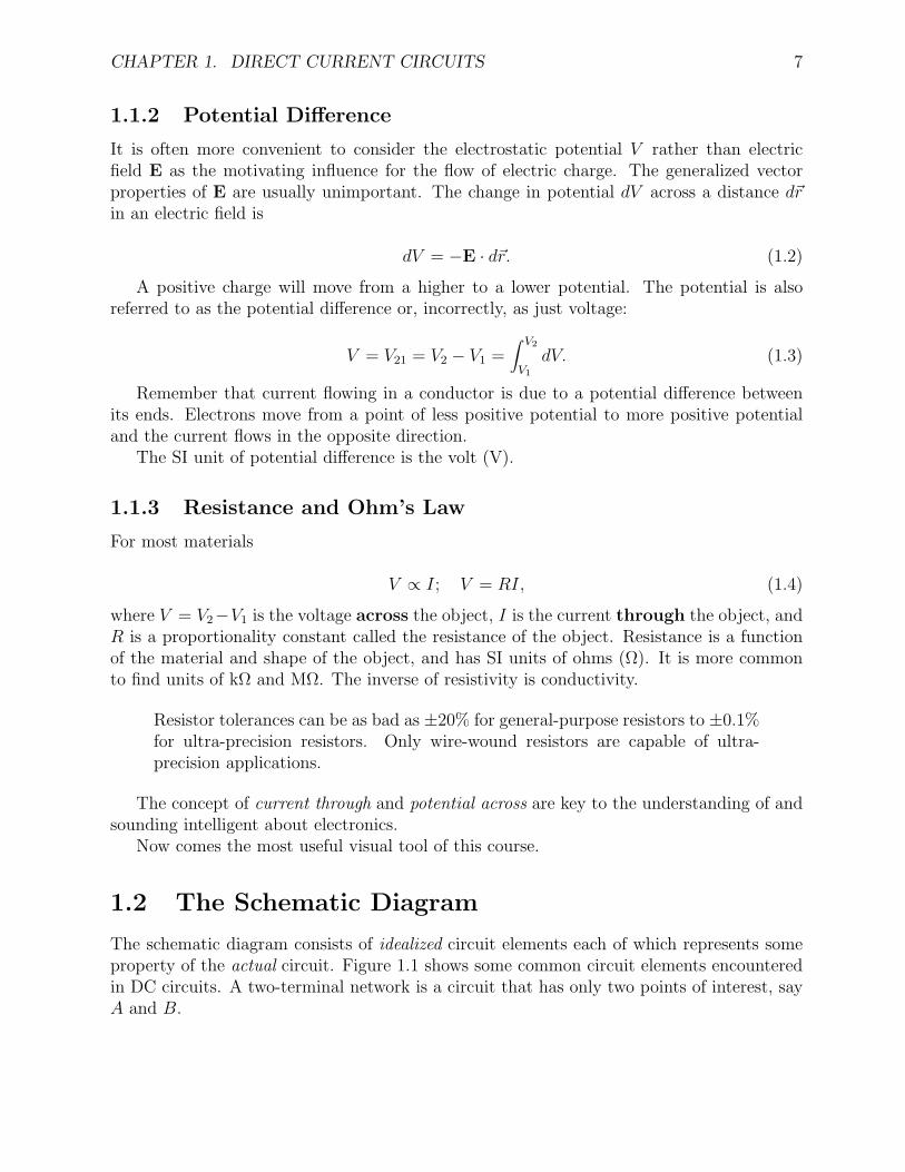
1.2 The Schematic Diagram
The schematic diagram consists of idealized circuit elements each of which represents someproperty of the actual circuit. Figure 1.1 shows some common circuit elements encounteredin DC circuits. A two-terminal network is a circuit that has only two points of interest, sayA and B.
CHAPTER 1. DIRECT CURRENT CIRCUITS 8
+V
(a)
I
(b)
R
(c)
Figure 1.1: Common circuit elements encountered in DC circuits: a) ideal voltage source,b) ideal current source and c) resistor.
1.2.1 Electromotive Force (EMF)
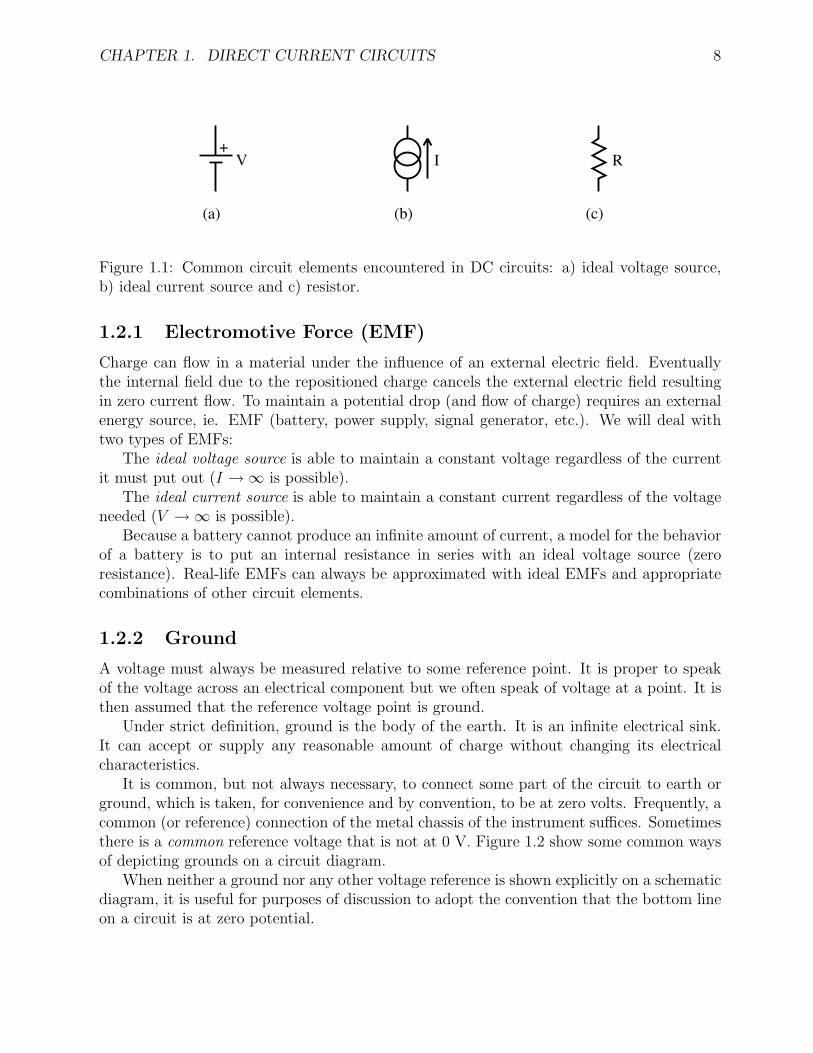
Charge can flow in a material under the influence of an external electric field. Eventuallythe internal field due to the repositioned charge cancels the external electric field resultingin zero current flow. To maintain a potential drop (and flow of charge) requires an externalenergy source, ie. EMF (battery, power supply, signal generator, etc.). We will deal withtwo types of EMFs:
The ideal voltage source is able to maintain a constant voltage regardless of the currentit must put out (I → ∞ is possible).
The ideal current source is able to maintain a constant current regardless of the voltageneeded (V → ∞ is possible).
Because a battery cannot produce an infinite amount of current, a model for the behaviorof a battery is to put an internal resistance in series with an ideal voltage source (zeroresistance). Real-life EMFs can always be approximated with ideal EMFs and appropriatecombinations of other circuit elements.
1.2.2 Ground
A voltage must always be measured relative to some reference point. It is proper to speakof the voltage across an electrical component but we often speak of voltage at a point. It isthen assumed that the reference voltage point is ground.
Under strict definition, ground is the body of the earth. It is an infinite electrical sink.It can accept or supply any reasonable amount of charge without changing its electricalcharacteristics.
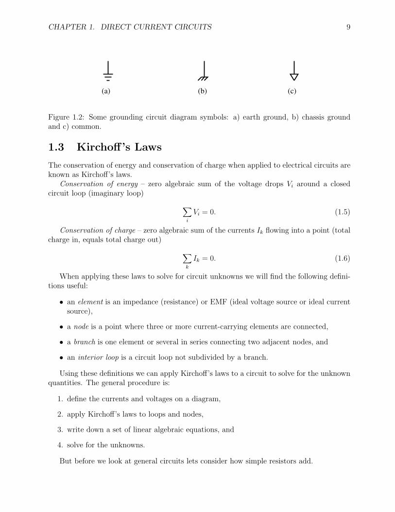
It is common, but not always necessary, to connect some part of the circuit to earth orground, which is taken, for convenience and by convention, to be at zero volts. Frequently, acommon (or reference) connection of the metal chassis of the instrument suffices. Sometimesthere is a common reference voltage that is not at 0 V. Figure 1.2 show some common waysof depicting grounds on a circuit diagram.
When neither a ground nor any other voltage reference is shown explicitly on a schematicdiagram, it is useful for purposes of discussion to adopt the convention that the bottom lineon a circuit is at zero potential.
CHAPTER 1. DIRECT CURRENT CIRCUITS 9
(a) (b) (c)
Figure 1.2: Some grounding circuit diagram symbols: a) earth ground, b) chassis groundand c) common.
1.3 Kirchoff’s Laws
The conservation of energy and conservation of charge when applied to electrical circuits areknown as Kirchoff’s laws.
Conservation of energy – zero algebraic sum of the voltage drops Vi around a closedcircuit loop (imaginary loop)
∑i
Vi = 0. (1.5)
Conservation of charge – zero algebraic sum of the currents Ik flowing into a point (totalcharge in, equals total charge out)
∑k
Ik = 0. (1.6)
When applying these laws to solve for circuit unknowns we will find the following defini-tions useful:
• an element is an impedance (resistance) or EMF (ideal voltage source or ideal currentsource),
• a node is a point where three or more current-carrying elements are connected,
• a branch is one element or several in series connecting two adjacent nodes, and
• an interior loop is a circuit loop not subdivided by a branch.
Using these definitions we can apply Kirchoff’s laws to a circuit to solve for the unknownquantities. The general procedure is:
1. define the currents and voltages on a diagram,
2. apply Kirchoff’s laws to loops and nodes,
3. write down a set of linear algebraic equations, and
4. solve for the unknowns.
But before we look at general circuits lets consider how simple resistors add.
CHAPTER 1. DIRECT CURRENT CIRCUITS 10
1.3.1 Series and Parallel Combinations of Resistors
Circuit elements are connected in series when a common current passes through each element.The equivalent resistance Req of a combination of resistors Ri connected in series is given bysumming the voltage drops across each resistor.
V =∑
i
Vi = I∑
i
Ri, (1.7)
Req =∑
i
Ri. (1.8)
If Rj Rk, where Rk are all the other resistors than Req ≈ Rj; the largest resistor wins.Circuit elements are connected in parallel when a common voltage is applied across each
element. The equivalent resistance Req of a combination of resistors Ri connected in parallelis given by summing the current through each resistor
I =∑
i
Ii =∑
i
V
Ri
, (1.9)
1
Req
=I
V=∑
i
1
Ri
, (1.10)
Req =
∏i Ri∑
i
∏j =i Rj
. (1.11)
If Rj Rk, where Rk are all the other resistors than Req ≈ Rj; the smallest resistor wins.The following “divider” circuits are useful combinations of resistors. Believe it or not,
they are a super useful concept that will often be used in one form or another; learn it.
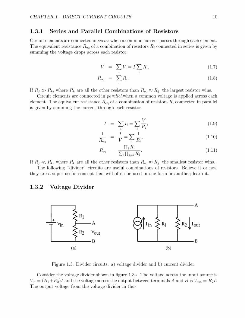
1.3.2 Voltage Divider
(a)
Vout
A
B
+Vin
R2
R1
(b)
A
B
I in R1 R2 Iout
Figure 1.3: Divider circuits: a) voltage divider and b) current divider.
Consider the voltage divider shown in figure 1.3a. The voltage across the input source isVin = (R1+R2)I and the voltage across the output between terminals A and B is Vout = R2I.The output voltage from the voltage divider in thus
CHAPTER 1. DIRECT CURRENT CIRCUITS 11
Vout =R2
R1 + R2
Vin. (1.12)
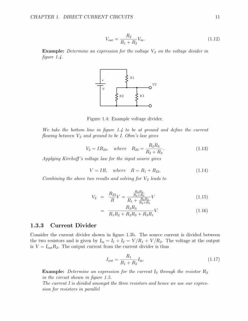
Example: Determine an expression for the voltage V2 on the voltage divider infigure 1.4.
V2V
+R1
R3R2
Figure 1.4: Example voltage divider.
We take the bottom line in figure 1.4 to be at ground and define the currentflowing between V2 and ground to be I. Ohm’s law gives
V2 = IR23, where R23 =R2R3
R2 + R3
. (1.13)
Applying Kirchoff’s voltage law for the input source gives
V = IR, where R = R1 + R23. (1.14)
Combining the above two results and solving for V2 leads to
V2 =R23
RV =
R2R3
R2+R3
R1 + R2R3
R2+R3
V (1.15)
=R2R3
R1R2 + R2R3 + R3R1
V. (1.16)
1.3.3 Current Divider
Consider the current divider shown in figure 1.3b. The source current is divided betweenthe two resistors and is given by Iin = I1 + I2 = V/R1 + V/R2 . The voltage at the outputis V = IoutR2 . The output current from the current divider is thus
Iout =R1
R1 + R2
Iin. (1.17)
Example: Determine an expression for the current I3 through the resistor R3
in the circuit shown in figure 1.5.The current I is divided amongst the three resistors and hence we use our expres-sion for resistors in parallel
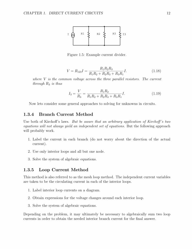
CHAPTER 1. DIRECT CURRENT CIRCUITS 12
I3I R3R2R1
Figure 1.5: Example current divider.
V = R123I =R1R2R3
R1R2 + R2R3 + R3R1
I. (1.18)
where V is the common voltage across the three parallel resistors. The currentthrough R3 is thus
I3 =V
R3
=R1R2
R1R2 + R2R3 + R3R1
I. (1.19)
Now lets consider some general approaches to solving for unknowns in circuits.
1.3.4 Branch Current Method
Use both of Kirchoff’s laws. But be aware that an arbitrary application of Kirchoff’s twoequations will not always yield an independent set of equations. But the following approachwill probably work.
1. Label the current in each branch (do not worry about the direction of the actualcurrent).
2. Use only interior loops and all but one node.
3. Solve the system of algebraic equations.
1.3.5 Loop Current Method
This method is also referred to as the mesh loop method. The independent current variablesare taken to be the circulating current in each of the interior loops.
1. Label interior loop currents on a diagram.
2. Obtain expressions for the voltage changes around each interior loop.
3. Solve the system of algebraic equations.
Depending on the problem, it may ultimately be necessary to algebraically sum two loopcurrents in order to obtain the needed interior branch current for the final answer.
CHAPTER 1. DIRECT CURRENT CIRCUITS 13
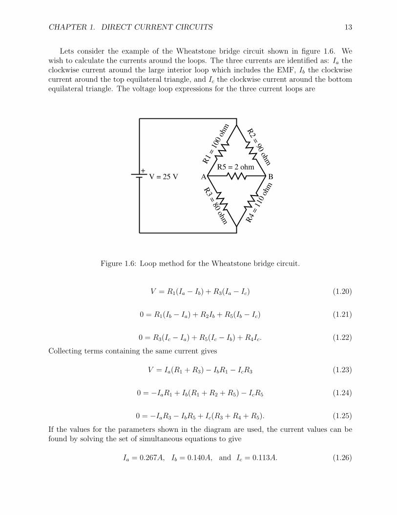
Lets consider the example of the Wheatstone bridge circuit shown in figure 1.6. Wewish to calculate the currents around the loops. The three currents are identified as: Ia theclockwise current around the large interior loop which includes the EMF, Ib the clockwisecurrent around the top equilateral triangle, and Ic the clockwise current around the bottomequilateral triangle. The voltage loop expressions for the three current loops are
+V = 25 V
R1
= 10
0 oh
m R2 = 90 ohm
R3 = 80 ohm R
4 =
110
ohm
R5 = 2 ohmA B
Figure 1.6: Loop method for the Wheatstone bridge circuit.
V = R1(Ia − Ib) + R3(Ia − Ic) (1.20)
0 = R1(Ib − Ia) + R2Ib + R5(Ib − Ic) (1.21)
0 = R3(Ic − Ia) + R5(Ic − Ib) + R4Ic. (1.22)
Collecting terms containing the same current gives
V = Ia(R1 + R3) − IbR1 − IcR3 (1.23)
0 = −IaR1 + Ib(R1 + R2 + R5) − IcR5 (1.24)
0 = −IaR3 − IbR5 + Ic(R3 + R4 + R5). (1.25)
If the values for the parameters shown in the diagram are used, the current values can befound by solving the set of simultaneous equations to give
Ia = 0.267A, Ib = 0.140A, and Ic = 0.113A. (1.26)
CHAPTER 1. DIRECT CURRENT CIRCUITS 14
Moreover, if we number the individual currents through each resistor using the same schemeas we have for each component (current through R1 is I1, R2 has I2, etc.) and identify I0 asthe current out of the battery, then
I0 = Ia = 0.267A (1.27)
I1 = Ia − Ib = 0.127A (1.28)
I2 = Ib = 0.140A (1.29)
I3 = Ia − Ic = 0.154A (1.30)
I4 = Ic = 0.113A (1.31)
I5 = Ib − Ic = 0.027A. (1.32)
These are the same currents that would be found using only Kirchoff’s equations; however,here we had to handle only three simultaneous equations instead of six.
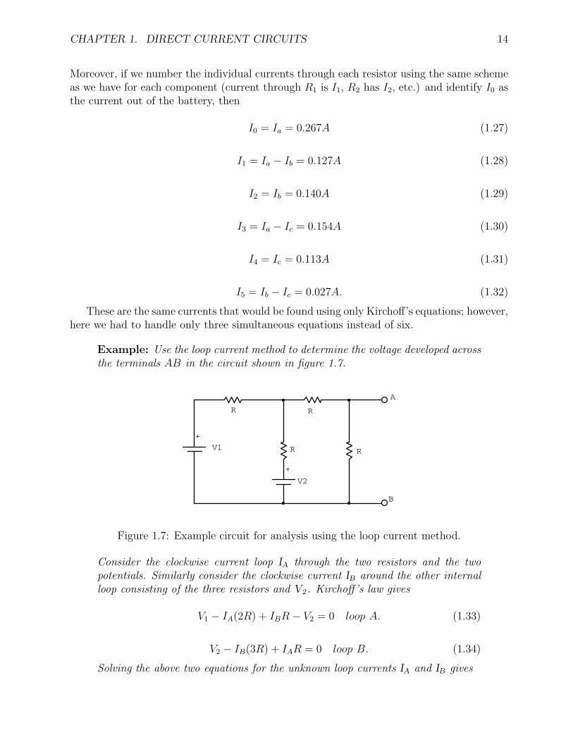
Example: Use the loop current method to determine the voltage developed acrossthe terminals AB in the circuit shown in figure 1.7.
+
+
V2
V1
B
A
RR
RR
Figure 1.7: Example circuit for analysis using the loop current method.
Consider the clockwise current loop IA through the two resistors and the twopotentials. Similarly consider the clockwise current IB around the other internalloop consisting of the three resistors and V2 . Kirchoff’s law gives
V1 − IA(2R) + IBR − V2 = 0 loop A. (1.33)
V2 − IB(3R) + IAR = 0 loop B. (1.34)
Solving the above two equations for the unknown loop currents IA and IB gives
CHAPTER 1. DIRECT CURRENT CIRCUITS 15
V1 − V2 = 2RIA − RIB (1.35)
V2 = −RIA + 3RIB, (1.36)
(V1 − V2
V2
)=
(2R −R−R 3R
)(IA
IB
)≡ R
(IA
IB
), (1.37)
R−1 =1
R
(3/5 1/51/5 2/5
), (1.38)
IA =1
R
[3
5(V1 − V2) +
1
5V2
]=
1
R
(3
5V1 − 2
5V2
)(1.39)
IB =1
R
[1
5(V1 − V2) +
2
5V2
]=
1
R
(1
5V1 +
1
5V2
). (1.40)
The voltage across AB is given simply by
VAB = IBR (1.41)
=1
5(V1 + V2). (1.42)
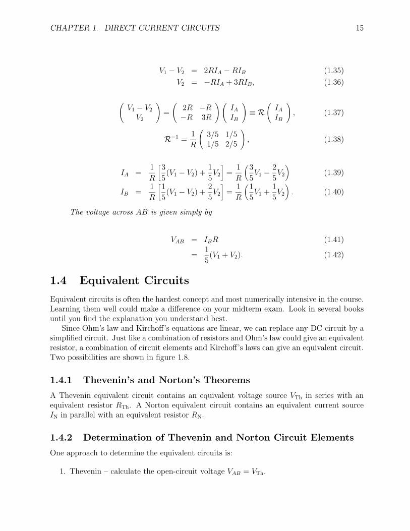
1.4 Equivalent Circuits
Equivalent circuits is often the hardest concept and most numerically intensive in the course.Learning them well could make a difference on your midterm exam. Look in several booksuntil you find the explanation you understand best.
Since Ohm’s law and Kirchoff’s equations are linear, we can replace any DC circuit by asimplified circuit. Just like a combination of resistors and Ohm’s law could give an equivalentresistor, a combination of circuit elements and Kirchoff’s laws can give an equivalent circuit.Two possibilities are shown in figure 1.8.
1.4.1 Thevenin’s and Norton’s Theorems
A Thevenin equivalent circuit contains an equivalent voltage source VTh in series with anequivalent resistor RTh. A Norton equivalent circuit contains an equivalent current sourceIN in parallel with an equivalent resistor RN.
1.4.2 Determination of Thevenin and Norton Circuit Elements
One approach to determine the equivalent circuits is:
1. Thevenin – calculate the open-circuit voltage VAB = VTh.
CHAPTER 1. DIRECT CURRENT CIRCUITS 16
(a)B
A
+VTh
RTh
(b)
A
B
I N RN
Figure 1.8: Thevenin and Norton equivalent circuits.
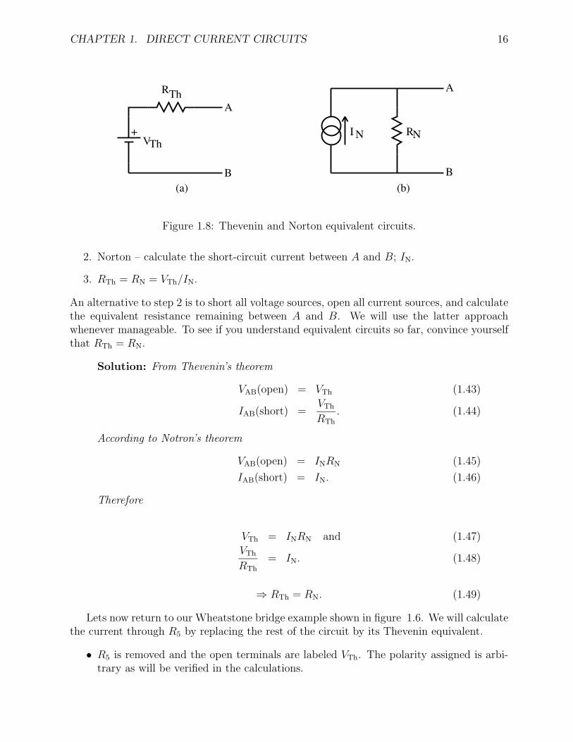
2. Norton – calculate the short-circuit current between A and B; IN.
3. RTh = RN = VTh/IN.
An alternative to step 2 is to short all voltage sources, open all current sources, and calculatethe equivalent resistance remaining between A and B. We will use the latter approachwhenever manageable. To see if you understand equivalent circuits so far, convince yourselfthat RTh = RN.
Solution: From Thevenin’s theorem
VAB(open) = VTh (1.43)
IAB(short) =VTh
RTh
. (1.44)
According to Notron’s theorem
VAB(open) = INRN (1.45)
IAB(short) = IN. (1.46)
Therefore
VTh = INRN and (1.47)
VTh
RTh
= IN. (1.48)
⇒ RTh = RN. (1.49)
Lets now return to our Wheatstone bridge example shown in figure 1.6. We will calculatethe current through R5 by replacing the rest of the circuit by its Thevenin equivalent.
• R5 is removed and the open terminals are labeled VTh. The polarity assigned is arbi-trary as will be verified in the calculations.
CHAPTER 1. DIRECT CURRENT CIRCUITS 17
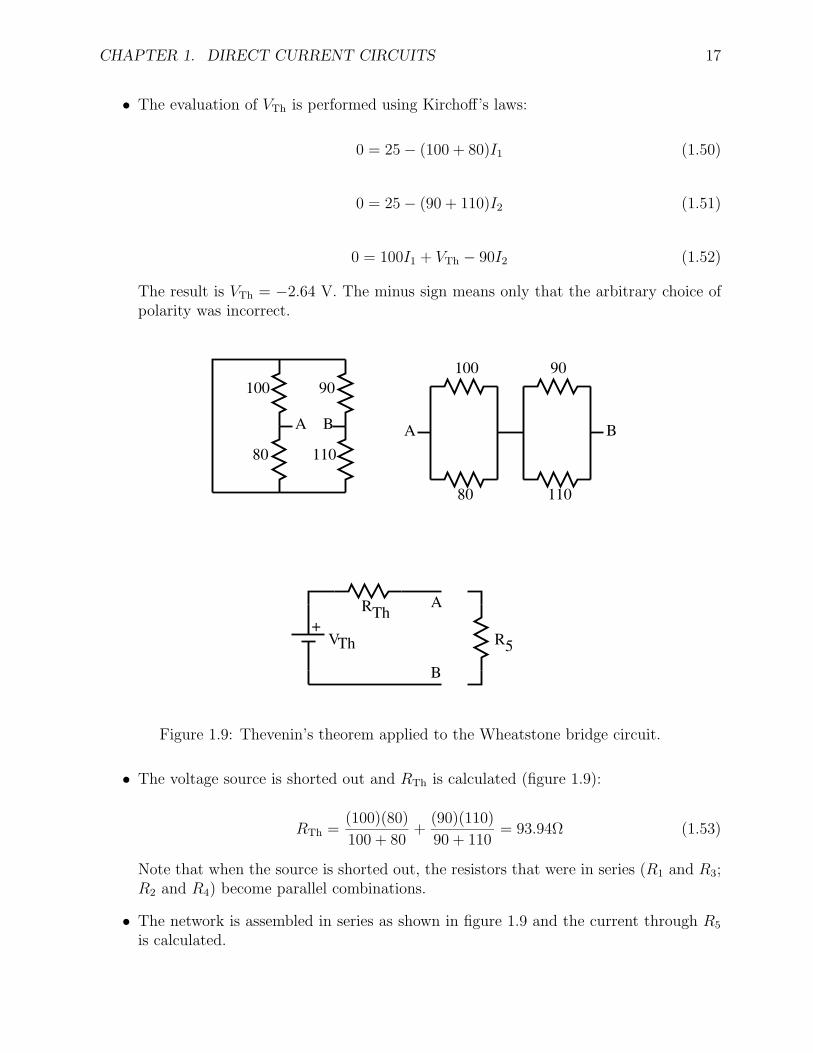
• The evaluation of VTh is performed using Kirchoff’s laws:
0 = 25 − (100 + 80)I1 (1.50)
0 = 25 − (90 + 110)I2 (1.51)
0 = 100I1 + VTh − 90I2 (1.52)
The result is VTh = −2.64 V. The minus sign means only that the arbitrary choice ofpolarity was incorrect.
A B
80
100
110
90
A B
80
100
110
90
B
A
+VTh
RTh
R5
Figure 1.9: Thevenin’s theorem applied to the Wheatstone bridge circuit.
• The voltage source is shorted out and RTh is calculated (figure 1.9):
RTh =(100)(80)
100 + 80+
(90)(110)
90 + 110= 93.94Ω (1.53)
Note that when the source is shorted out, the resistors that were in series (R1 and R3;R2 and R4) become parallel combinations.
• The network is assembled in series as shown in figure 1.9 and the current through R5
is calculated.
CHAPTER 1. DIRECT CURRENT CIRCUITS 18
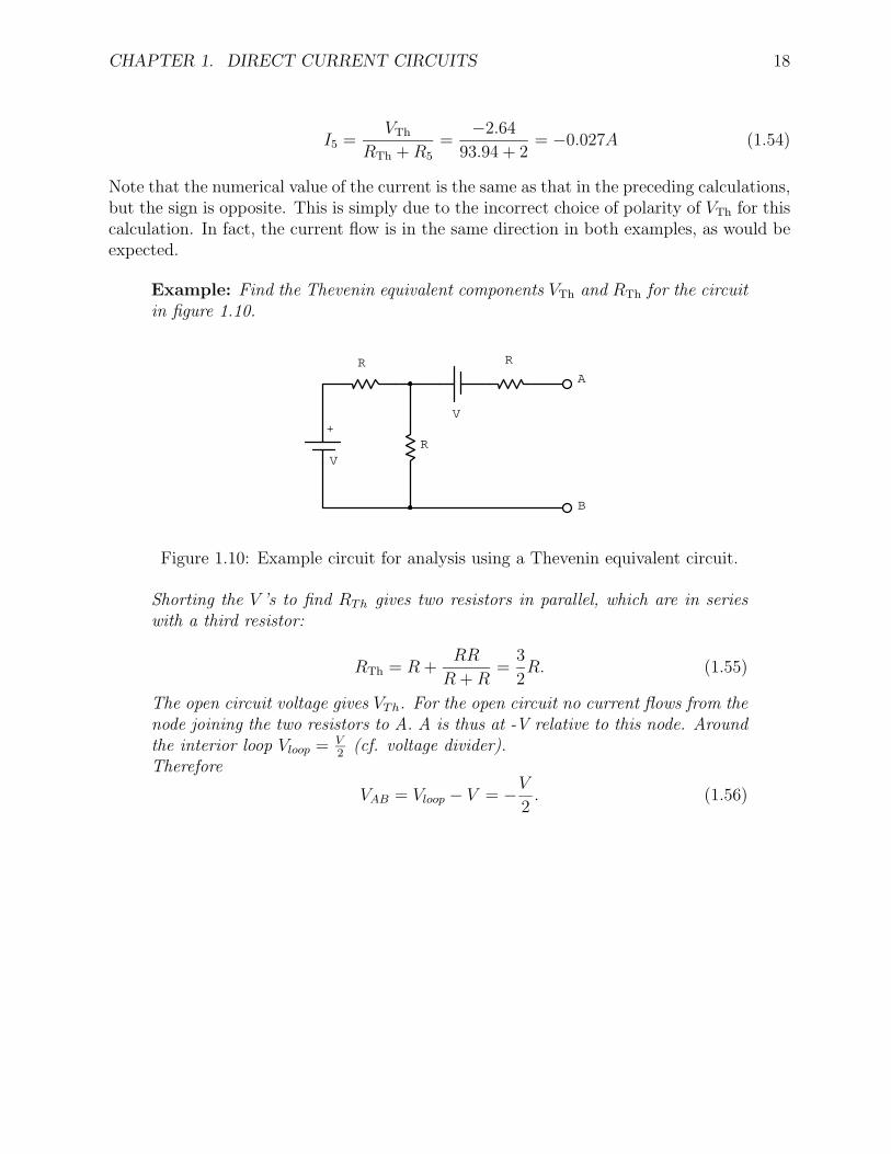
I5 =VTh
RTh + R5
=−2.64
93.94 + 2= −0.027A (1.54)
Note that the numerical value of the current is the same as that in the preceding calculations,but the sign is opposite. This is simply due to the incorrect choice of polarity of VTh for thiscalculation. In fact, the current flow is in the same direction in both examples, as would beexpected.
Example: Find the Thevenin equivalent components VTh and RTh for the circuitin figure 1.10.
+V
V
R
R
R
B
A
Figure 1.10: Example circuit for analysis using a Thevenin equivalent circuit.
Shorting the V ’s to find RTh gives two resistors in parallel, which are in serieswith a third resistor:
RTh = R +RR
R + R=
3
2R. (1.55)
The open circuit voltage gives VTh. For the open circuit no current flows from thenode joining the two resistors to A. A is thus at -V relative to this node. Aroundthe interior loop Vloop = V
2(cf. voltage divider).
Therefore
VAB = Vloop − V = −V
2. (1.56)
CHAPTER 1. DIRECT CURRENT CIRCUITS 19
1.5 Problems
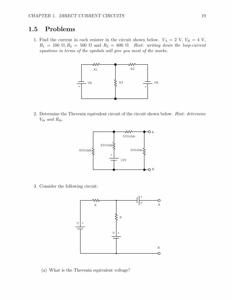
1. Find the current in each resister in the circuit shown below. VA = 2 V, VB = 4 V,R1 = 100 Ω, R2 = 500 Ω and R3 = 600 Ω. Hint: writing down the loop-currentequations in terms of the symbols will give you most of the marks.
++VA VBR3
R2R1
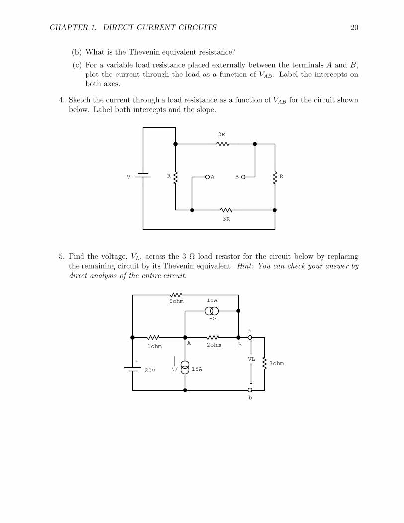
2. Determine the Thevenin equivalent circuit of the circuit shown below. Hint: determineVth and Rth.
B
A
+
10V
600ohm
600ohm
300ohm
300ohm
3. Consider the following circuit:
B
AR
R
+
+
+
V
V
V
(a) What is the Thevenin equivalent voltage?
CHAPTER 1. DIRECT CURRENT CIRCUITS 20
(b) What is the Thevenin equivalent resistance?
(c) For a variable load resistance placed externally between the terminals A and B,plot the current through the load as a function of VAB. Label the intercepts onboth axes.
4. Sketch the current through a load resistance as a function of VAB for the circuit shownbelow. Label both intercepts and the slope.
R
3R
2R
RBAV
5. Find the voltage, VL, across the 3 Ω load resistor for the circuit below by replacingthe remaining circuit by its Thevenin equivalent. Hint: You can check your answer bydirect analysis of the entire circuit.
||\/
VL
A
b
a
B
->
+
1ohm
20V 15A3ohm
2ohm
15A6ohm
Chapter 2
Alternating Current Circuits
We now consider circuits where the currents and voltages may vary with time (V = V (t),I = I(t) (also Q = Q(t))). These lectures will concentrate on the special case in which thesignals are periodic, with time average values of zero (〈v(t)〉 = 〈i(t)〉 = 0). Circuits withthese signals are referred to as alternating current (AC) circuits. In general signals will haveboth DC and AC properties (v(t) = VAC(t) + VDC). We will concentrate only on the ACcomponents and assume that the DC properties can be treated separately using the methodsof the previous lectures.
The algebraic equations representing Kirchoff’s laws for DC circuits will take the formof differential equations for AC circuits. So now is a good time to review your differentialequations and complex number theory because we will use it.
2.1 AC Circuit Elements
In physical terms, EMFs can be regarded as circuit elements which put energy into a circuitand a resistor R as an element which removes energy from a circuit. The energy is dissipatedin the resistor as heat. In AC circuits we have the additional circuit elements, capacitance Cand inductance L, which store energy in electric and magnetic fields respectively. C and Lare referred to as reactive elements while R is a resistive element. All three of these elementare considered passive elements. We will encounter active circuit elements in the lecturesto follow. For simplicity we will ignore radiation that might be emitted by high frequencycircuits.
2.1.1 Capacitance
The fundamental property of a capacitor is that it can store charge and hence electric fieldenergy. The capacitance C between two appropriate surfaces is defined by
V =Q
C, (2.1)
where V is the potential difference between the surfaces and Q is the magnitude of the chargedistributed on either surface.
21
CHAPTER 2. ALTERNATING CURRENT CIRCUITS 22
In terms of current, I = dQ/dt implies
dV
dt=
1
C
dQ
dt=
I
C. (2.2)
In electronics we take I = ID (displacement current). In other words, the current flow-ing from or to the capacitor is taken to be equal to the displacement current through thecapacitor. You should be able to show that capacitors add linearly when placed in parallel.
There are four principle functions of a capacitor in a circuit.
1. Since Q and E can be stored a capacitor can be used as a (non-ideal) source of I andV .
2. Since a capacitor passes AC current but not DC current it can be used to connectparts of a circuit that must operate at different DC voltage levels.
3. A capacitor and resistor in series will limit current and hence smooth sharp edges involtage signals.
4. Charging or discharging a capacitor with a constant current results in the capacitorhaving a voltage signal with a constant slope, ie. dV/dt = I/C = constant if I is aconstant.
Some capacitors (electrolytic) are asymmetric devices with a polarity that must behooked-up in a definite way. You will learn this in the lab. The SI unit for capacitanceis farad (F). The capacitance in a circuit is typically measured in µF or pF. Non-ideal cir-cuits will have stray capacitance, leakage currents and inductive coupling at high frequency.Although important in real circuit design we will slip over these nasties at this point.
Capacitors can be obtained in various tolerance ratings from ±20% to ±0.5%.Because of dimensional changes, capacitors have a high temperature dependenceof capacitance. A capacitor does not hold a charge indefinitely because the dielec-tric is never a perfect insulator. Capacitors are rated for leakage, the conductionthrough the dielectric, by the leakage resistance-capacitance product in MΩ ·µF.High temperature increases leakage.
2.1.2 Inductance
Faraday’s law applied to an inductor states that a changing current induces a back EMFthat opposes the change. Or
V = VA − VB = LdI
dt. (2.3)
Where V is the voltage across the inductor and L is the inductance measured in henry (H).The more common units encountered in circuits are µH and mH.
The inductance will tend to smooth sudden changes in current just as the capacitancesmoothes sudden changes in voltage. Of course, if the current is constant there will be no
CHAPTER 2. ALTERNATING CURRENT CIRCUITS 23
induced EMF. So unlike the capacitor which behaves like an open-circuit in DC circuits, aninductor behaves like a short-circuit in DC circuits.
Applications using inductors are less common than those using capacitors, but inductorsare very common in high frequency circuits. We will again skip over the unpleasantness –that non-ideal inductors have some resistance and some capacitance.
Inductors are never pure inductances because there is always some resistance inand some capacitance between the coil windings. When choosing an inductor(occasionally called a choke) for a specific application, it is necessary to considerthe value of the inductance, the DC resistance of the coil, the current-carryingcapacity of the coil windings, the breakdown voltage between the coil and theframe, and the frequency range in which the coil is designed to operate. Toobtain a very high inductance it is necessary to have a coil of many turns. Theinductance can be further increased by winding the coil on a closed-loop iron orferrite core. To obtain as pure an inductance as possible, the DC resistance ofthe windings should be reduced to a minimum. This can be done by increasingthe wire size, which of course, increases the size of the choke. The size of the wirealso determines the current-handling capacity of the choke since the work donein forcing a current through a resistance is converted to heat in the resistance.Magnetic losses in an iron core also account for some heating, and this heatingrestricts any choke to a certain safe operating current. The windings of the coilmust be insulated from the frame as well as from each other. Heavier insulation,which necessarily makes the choke more bulky, is used in applications wherethere will be a high voltage between the frame and the winding. The lossessustained in the iron core increases as the frequency increases. Large inductors,rated in henries, are used principally in power applications. The frequency inthese circuits is relatively low, generally 60 Hz or low multiples thereof. In high-frequency circuits, such as those found in FM radios and television sets, verysmall inductors (of the order of microhenries) are frequently used.
2.2 Circuit Equations
Recall that voltage V is related to current I, via the passive DC circuit element resistanceR, by Ohm’s law V = IR. Analogously, the change in voltage and change in current arerelated to the current and voltage, via the passive AC circuit elements C and L, by
dV
dt=
I
Cand V = L
dI
dt. (2.4)
Applying the above three equations, along with Kirchoff’s loop rule, to AC circuits resultsin a set of differential equations. These differential equations are linear with constant coeffi-cients and can easily be solved for Q(t), I(t), and V (t). In general the solutions will consistof a transient response and a steady-state response. The transient response describes thereturn to equilibrium after the EMFs change suddenly. The steady-state response describesthe long term behaviour when the circuit is driven by a sinusoidal source.
CHAPTER 2. ALTERNATING CURRENT CIRCUITS 24
We will first consider the transient response. This will be one of the few times we considernon-oscillating AC behaviour. Since Ohm’s law and Kirchoff’s laws are linear we can usecomplex exponential signals and take real or imaginary parts in the end. This is not truefor power, since it is non-linear (product of signals).
2.2.1 RC Circuit
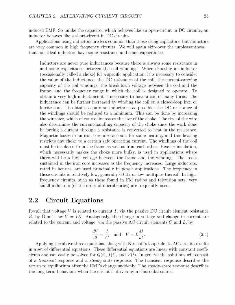
Consider the resistor R and capacitance C in the circuit loop in figure 2.1. Notice that thereis no source.
CR
Figure 2.1: RC circuit.
We start with a differential version of Kirchoff’s voltage law.
d
dt
∑i
Vi =∑
i
dVi
dt= 0. (2.5)
When applied to our circuit
dVC
dt+
dVR
dt= 0, (2.6)
where VC is the voltage drop across the capacitor and VR is the voltage drop across theresistor.
The change in the voltage drop across the capacitor is given by our previous expression,
dVC
dt=
I
C. (2.7)
The change in the voltage drop across the resistor can be obtained from Ohm’s law
VR = RI ⇒ dVR
dt= R
dI
dt. (2.8)
Substituting these changes in voltage into Kirchoff’s equation gives
I
C+ R
dI
dt= 0, (2.9)
where the current due to the flow of charge on or off the capacitor is the same as throughthe resistor.
Now we need some initial conditions. Notice that although the capacitor behaves as anopen circuit to DC, current must flow to charge or discharge the capacitor. Lets take the
CHAPTER 2. ALTERNATING CURRENT CIRCUITS 25
case where the capacitor is initially charged and then the circuit is closed and the chargeis allowed to drain off the capacitor (eg. closing a switch). The resulting current will flowthrough the resistor.
Solving for the current we obtain
I(t) = I0e−t/RC , (2.10)
where I(t = 0) = I0 is the initial current given by Ohm’s law
I0 =V0
R. (2.11)
Using a time dependent version of Ohm’s law we can solve for the voltage across theresistor
V (t) = RI(t) = RI0e−t/RC = V0e
−t/RC = V0e−t/τ , (2.12)
where V (t = 0) ≡ V0 is the initial voltage across the capacitor and τ ≡ RC is the commonlydefined time constant of the decay. You should also be able to solve for the voltage acrossthe capacitor and charge on the capacitor.
For the case of an applying voltage VB being suddenly placed into the circuit (insertinga battery) the capacitor is initially not charged and the voltage across the capacitor is
V (t) = VB(1 − e−t/τ ). (2.13)
In the first case, current and voltage exponentially decay away with time constant τ whenthe switch is closed. The charge flows off the capacitor and through the resistor. The energyinitially stored in the capacitor is dissipated in the resistor.
In the second case the capacitor charges to a voltage VB until no current flows and hencethe voltage drop across the resistor is zero. Energy from the battery is stored in the capacitor.
In both cases the characteristic RC time constant occurs. In general this is true of allresistor-capacitor combinations and will be important throughout the course.
2.2.2 RL Circuit
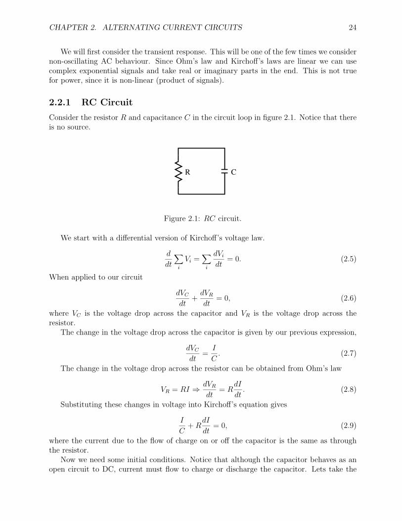
The response of the RL circuit, shown in figure 2.2, is similar to that of the RC circuit.There are however some significant differences.
R L
Figure 2.2: RL circuit.
CHAPTER 2. ALTERNATING CURRENT CIRCUITS 26
If a battery is inserted into the circuit the current raises quickly from zero to some finitevalue. The EMF generated in the inductor impedes the current flow until it is constant.
The expression for the current in the RL circuit is
i(t) =VB
R(1 − e−tR/L) (2.14)
where the time constant is now
τ =L
R. (2.15)
The voltage across the resistor is an increasing exponential unlike the RC circuit inwhich the voltage across the resistor decreased exponentially. Likewise, the voltage acrossthe inductor decreases with time while in the RC circuit the voltage across the capacitorincreased with time.
There are other initial conditions we could work with in this circuit but these can nowbe worked out by the student.
2.2.3 LC Circuit
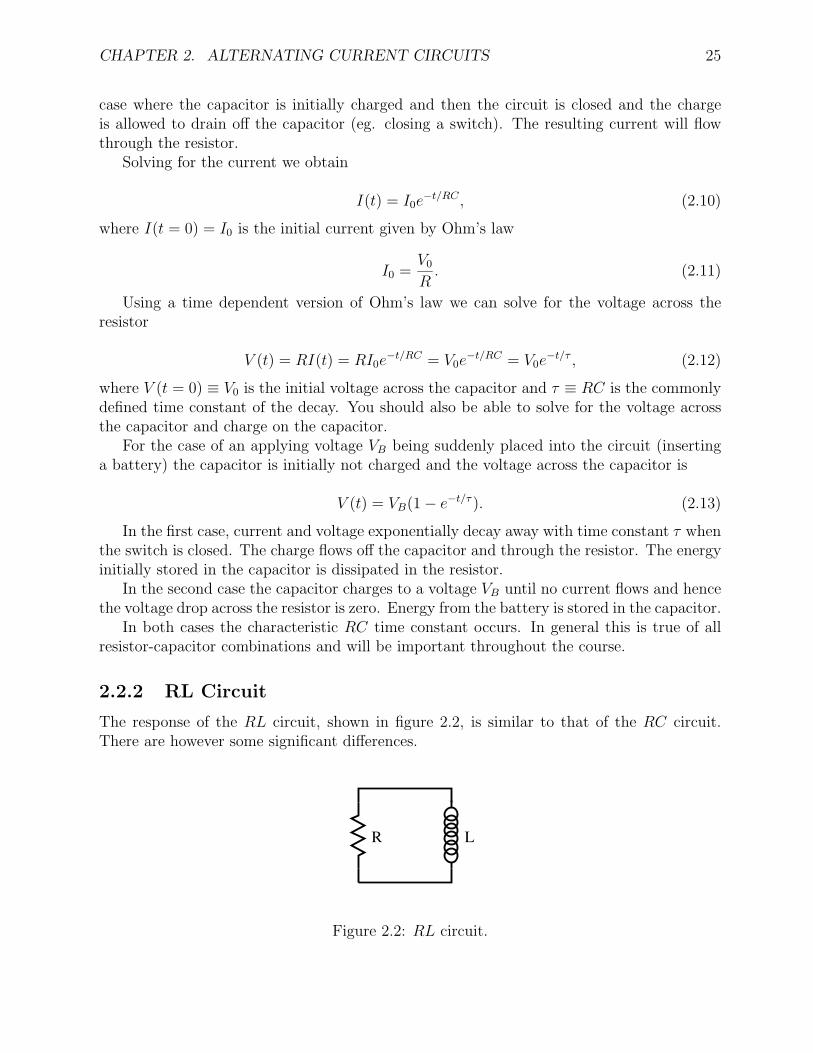
Lets now consider the LC circuit in figure 2.3 which has no resistive element.
CL
Figure 2.3: LC circuit.
Kirchoff’s voltage law applied to the loop is
VL + VC = 0. (2.16)
Substituting our previous expressions for VL and VC gives
LdI
dt+
Q
C= 0. (2.17)
Using I = dQ/dt gives
Ld2Q
dt2+
Q
C= 0. (2.18)
The circuit equation is second-order in Q and one possible solution is
Q(t) = Q0 cos(ωt + φ), (2.19)
CHAPTER 2. ALTERNATING CURRENT CIRCUITS 27
where Q(t = 0) = Q0 is the initial charge on the capacitor and φ is an arbitrary phaseconstant. Considering the cases of Q0 = Qmax, gives φ = 0. The angular frequency ω istotally determined by the other parameters of the circuit
ω2 = 1/(LC) (2.20)
and ωr ≡ 1/√
LC is the natural or resonance frequency of the circuit.We can also solve for the current and voltage across the capacitor
Q(t) = Q0 cos(ωrt), (2.21)
I(t) =dQ
dt= −Q0ωr sin(ωrt), (2.22)
= −I0 sin(ωrt) = I0 cos(ωrt + π/2), and (2.23)
V (t) =Q(t)
C=
Q0
Ccos(ωrt) = V0 cos(ωrt). (2.24)
Notice that unlike the transient current and voltage responses of the RC and RL circuits,the LC circuit oscillates. The energy in the circuit is shared back and forth between theinductor and capacitor.
2.2.4 RCL Circuit
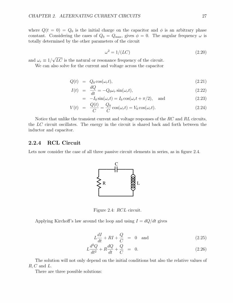
Lets now consider the case of all three passive circuit elements in series, as in figure 2.4.
R
C
L
Figure 2.4: RCL circuit.
Applying Kirchoff’s law around the loop and using I = dQ/dt gives
LdI
dt+ RI +
Q
C= 0 and (2.25)
Ld2Q
dt2+ R
dQ
dt+
Q
C= 0. (2.26)
The solution will not only depend on the initial conditions but also the relative values ofR,C and L.
There are three possible solutions:
CHAPTER 2. ALTERNATING CURRENT CIRCUITS 28
1. under damped (R2 < 4L/C): Ae−t/τ cos(ωt + φ),
2. over damped (R2 > 4L/C): A1e−t/τ1 + A2e
−t/τ2 , and
3. critically damped (R2 = 4L/C): (A1 + A2t)e−t/τ .
RCL circuits have a variety of properties, especially when driven by sinusoidal sources,which will not be investigated here. My aim is simply to expose you to the area and get onto more interesting topics. Driven oscillating systems also appear in other areas of physicsand hopefully you will encounter them there. The detailed considerations lead to discussionson resonance and quality-factor Q.
2.3 Sinusoidal Sources and Complex Impedance
We now consider current and voltage sources with time average values of zero. We will useperiodic signals but the observation time could well be less than one period. Periodic signalsare also useful in the sense that arbitrary signals can usually be expanded in terms of aFourier series of periodic signals. Lets start with
v(t) = V0 cos(ωt + φV ) and (2.27)
i(t) = I0 cos(ωt + φI). (2.28)
Notice that I have now switched to lowercase symbols. Lowercase is generally used for ACquantities while uppercase is reserved for DC values.
Now is the time to get into complex notation since it will make our discussion easier andis encountered often in electronics. The above voltage and current signals can be written
v(t) = V0ej(ωt+φV ) and (2.29)
i(t) = I0ej(ωt+φI). (2.30)
To be cleaver we will define one EMF in the circuit to have φ = 0. In other words, wewill pick t = 0 to be at the peak of one signal. The vector notation is used to remind usthat complex numbers can be considered as vectors in the complex plane. Although not socommon in physics, in electronics we refer to these vectors as phasors. Hence you shouldnow review complex notation.
The presence of sinusoidal v(t) ori(t) in circuits will result in an inhomogeneous differen-tial equation with a time-dependent source term. The solution will contain sinusoidal termswith the source frequency.
The extension of Ohm’s law to AC circuits can be written as
v(ω, t) = Z(ω)i(ω, t), (2.31)
where ω is the source frequency. Z is a generalized resistance referred to as the impedance.We can cancel out the common time dependent factors to obtain
CHAPTER 2. ALTERNATING CURRENT CIRCUITS 29
v(ω) = Z(ω)i(ω) (2.32)
and hence you see the power of the complex notation. For a physically quantity we take theamplitude of the real signal
|v(ω)| = |Z(ω)||i(ω)|. (2.33)
We will now examine each circuit element in turn with a voltage source to deduce itsimpedance.
2.3.1 Resistive Impedance
Kirchoff’s voltage law for a voltage source and resistor is
v(t) − Ri(t) = 0. (2.34)
Trying the solutions
i(t) =iejωt and v(t) = vejωt (2.35)
leads to
v = Ri ⇒ ZR = R. (2.36)
The impedance is equal to the resistance, as expected.
2.3.2 Capacitive Impedance
Kirchoff’s voltage law for a voltage source and capacitor is
v(t) − q(t)
C= 0. (2.37)
Or
dv(t)
dt−
i(t)
C= 0. (2.38)
Solving this equation gives
jωv =i
C⇒ ZC =
1
jωC(2.39)
For DC circuits ω = 0 and hence ZC → ∞. The capacitor acts like an open circuit(infinite resistance) in a DC circuit.
CHAPTER 2. ALTERNATING CURRENT CIRCUITS 30
2.3.3 Inductive Impedance
Kirchoff’s voltage law for a voltage source and inductor is
v(t) − Ldi(t)
dt= 0. (2.40)
Solving this equation gives
v = jωLi ⇒ ZL = jωL. (2.41)
For DC circuits ω = 0 and hence ZL = 0. There is no voltage drop across an inductor inDC (zero resistance).
2.3.4 Combined Impedances
We now know the impedance for each of our passive circuit elements:
ZR = R; ZL = jωL; ZC = −j/(ωC). (2.42)
The equivalent impedance of a circuit can be obtained by using the following rules forcombining impedances.In series
Zeq =∑
i
Zi. (2.43)
In parallel
Zeq =
∏i Zi∑
i
∏j =i Zj
. (2.44)
Appealing to the complex notation we can write
Zeq = R + jX(ω), (2.45)
where R is the resistance and X is called the reactance (always a function of ω).For a series combination of R, L and C
Zeq = R + jωL +1
jωC, (2.46)
= R + j(ωL − 1
ωC
). (2.47)
(ωL − 1/ωC) = 0 gives a special frequency, ω = 1/√
LC.
Example: An inductor and capacitor in parallel form the tank circuit shown infigure 2.5.
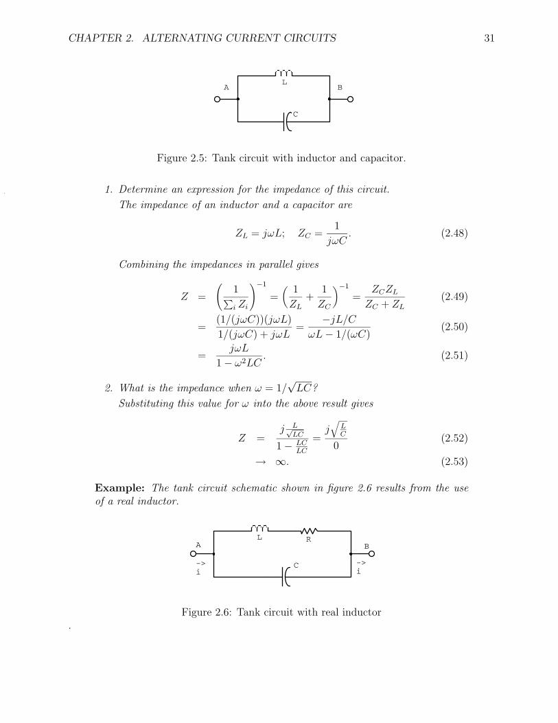
CHAPTER 2. ALTERNATING CURRENT CIRCUITS 31
BA
C
L
Figure 2.5: Tank circuit with inductor and capacitor.
1. Determine an expression for the impedance of this circuit.
The impedance of an inductor and a capacitor are
ZL = jωL; ZC =1
jωC. (2.48)
Combining the impedances in parallel gives
Z =
(1∑i Zi
)−1
=(
1
ZL
+1
ZC
)−1
=ZCZL
ZC + ZL
(2.49)
=(1/(jωC))(jωL)
1/(jωC) + jωL=
−jL/C
ωL − 1/(ωC)(2.50)
=jωL
1 − ω2LC. (2.51)
2. What is the impedance when ω = 1/√
LC?
Substituting this value for ω into the above result gives
Z =j L√
LC
1 − LCLC
=j√
LC
0(2.52)
→ ∞. (2.53)
Example: The tank circuit schematic shown in figure 2.6 results from the useof a real inductor.
->i
->i
BA
C
RL
Figure 2.6: Tank circuit with real inductor.
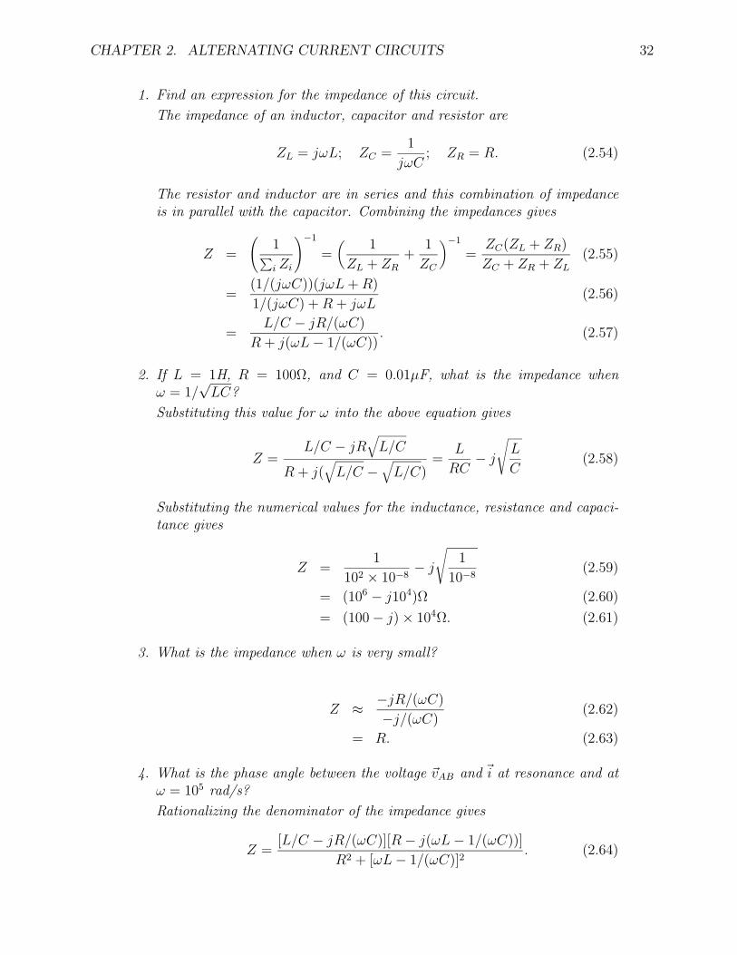
CHAPTER 2. ALTERNATING CURRENT CIRCUITS 32
1. Find an expression for the impedance of this circuit.
The impedance of an inductor, capacitor and resistor are
ZL = jωL; ZC =1
jωC; ZR = R. (2.54)
The resistor and inductor are in series and this combination of impedanceis in parallel with the capacitor. Combining the impedances gives
Z =
(1∑i Zi
)−1
=(
1
ZL + ZR
+1
ZC
)−1
=ZC(ZL + ZR)
ZC + ZR + ZL
(2.55)
=(1/(jωC))(jωL + R)
1/(jωC) + R + jωL(2.56)
=L/C − jR/(ωC)
R + j(ωL − 1/(ωC)). (2.57)
2. If L = 1H, R = 100Ω, and C = 0.01µF, what is the impedance whenω = 1/
√LC?
Substituting this value for ω into the above equation gives
Z =L/C − jR
√L/C
R + j(√
L/C −√
L/C)=
L
RC− j
√L
C(2.58)
Substituting the numerical values for the inductance, resistance and capaci-tance gives
Z =1
102 × 10−8− j
√1
10−8(2.59)
= (106 − j104)Ω (2.60)
= (100 − j) × 104Ω. (2.61)
3. What is the impedance when ω is very small?
Z ≈ −jR/(ωC)
−j/(ωC)(2.62)
= R. (2.63)
4. What is the phase angle between the voltage vAB and i at resonance and atω = 105 rad/s?
Rationalizing the denominator of the impedance gives
Z =[L/C − jR/(ωC)][R − j(ωL − 1/(ωC))]
R2 + [ωL − 1/(ωC)]2. (2.64)
CHAPTER 2. ALTERNATING CURRENT CIRCUITS 33
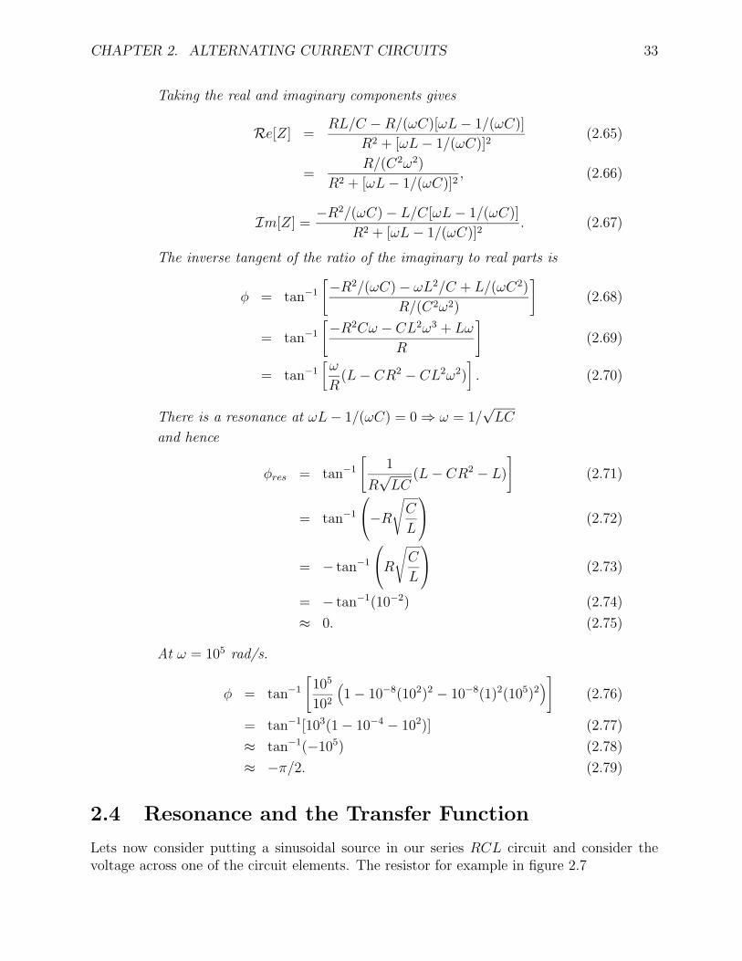
Taking the real and imaginary components gives
Re[Z] =RL/C − R/(ωC)[ωL − 1/(ωC)]
R2 + [ωL − 1/(ωC)]2(2.65)
=R/(C2ω2)
R2 + [ωL − 1/(ωC)]2, (2.66)
Im[Z] =−R2/(ωC) − L/C[ωL − 1/(ωC)]
R2 + [ωL − 1/(ωC)]2. (2.67)
The inverse tangent of the ratio of the imaginary to real parts is
φ = tan−1
[−R2/(ωC) − ωL2/C + L/(ωC2)
R/(C2ω2)
](2.68)
= tan−1
[−R2Cω − CL2ω3 + Lω
R
](2.69)
= tan−1[ω
R(L − CR2 − CL2ω2)
]. (2.70)
There is a resonance at ωL − 1/(ωC) = 0 ⇒ ω = 1/√
LC
and hence
φres = tan−1
[1
R√
LC(L − CR2 − L)
](2.71)
= tan−1
−R
√C
L
(2.72)
= − tan−1
R
√C
L
(2.73)
= − tan−1(10−2) (2.74)
≈ 0. (2.75)
At ω = 105 rad/s.
φ = tan−1
[105
102
(1 − 10−8(102)2 − 10−8(1)2(105)2
)](2.76)
= tan−1[103(1 − 10−4 − 102)] (2.77)
≈ tan−1(−105) (2.78)
≈ −π/2. (2.79)
2.4 Resonance and the Transfer Function
Lets now consider putting a sinusoidal source in our series RCL circuit and consider thevoltage across one of the circuit elements. The resistor for example in figure 2.7
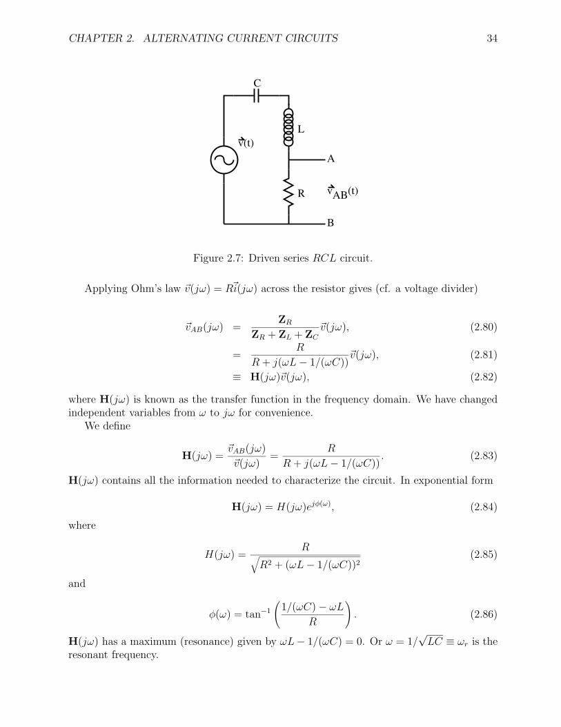
CHAPTER 2. ALTERNATING CURRENT CIRCUITS 34
v(t)
R
L
C
B
A
vAB(t)
Figure 2.7: Driven series RCL circuit.
Applying Ohm’s law v(jω) = Ri(jω) across the resistor gives (cf. a voltage divider)
vAB(jω) =ZR
ZR + ZL + ZC
v(jω), (2.80)
=R
R + j(ωL − 1/(ωC))v(jω), (2.81)
≡ H(jω)v(jω), (2.82)
where H(jω) is known as the transfer function in the frequency domain. We have changedindependent variables from ω to jω for convenience.
We define
H(jω) =vAB(jω)
v(jω)=
R
R + j(ωL − 1/(ωC)). (2.83)
H(jω) contains all the information needed to characterize the circuit. In exponential form
H(jω) = H(jω)ejφ(ω), (2.84)
where
H(jω) =R√
R2 + (ωL − 1/(ωC))2(2.85)
and
φ(ω) = tan−1
(1/(ωC) − ωL
R
). (2.86)
H(jω) has a maximum (resonance) given by ωL− 1/(ωC) = 0. Or ω = 1/√
LC ≡ ωr is theresonant frequency.
CHAPTER 2. ALTERNATING CURRENT CIRCUITS 35
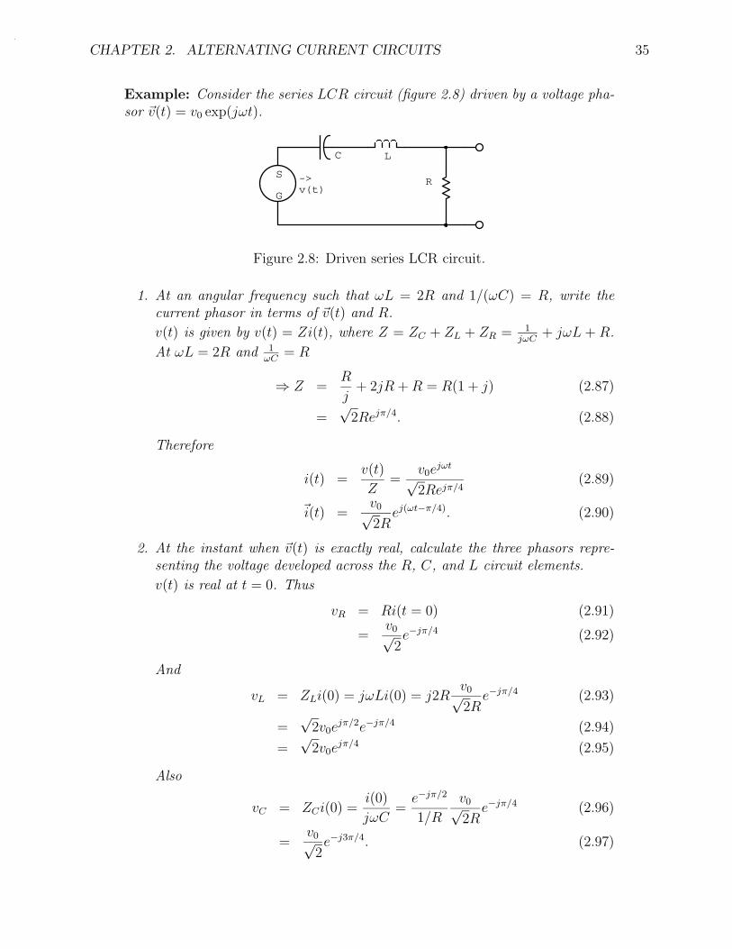
Example: Consider the series LCR circuit (figure 2.8) driven by a voltage pha-sor v(t) = v0 exp(jωt).
->v(t)
R
LC
S
G
Figure 2.8: Driven series LCR circuit.
1. At an angular frequency such that ωL = 2R and 1/(ωC) = R, write thecurrent phasor in terms of v(t) and R.
v(t) is given by v(t) = Zi(t), where Z = ZC + ZL + ZR = 1jωC
+ jωL + R.
At ωL = 2R and 1ωC
= R
⇒ Z =R
j+ 2jR + R = R(1 + j) (2.87)
=√
2Rejπ/4. (2.88)
Therefore
i(t) =v(t)
Z=
v0ejωt
√2Rejπ/4
(2.89)
i(t) =v0√2R
ej(ωt−π/4). (2.90)
2. At the instant when v(t) is exactly real, calculate the three phasors repre-senting the voltage developed across the R, C, and L circuit elements.
v(t) is real at t = 0. Thus
vR = Ri(t = 0) (2.91)
=v0√2e−jπ/4 (2.92)
And
vL = ZLi(0) = jωLi(0) = j2Rv0√2R
e−jπ/4 (2.93)
=√
2v0ejπ/2e−jπ/4 (2.94)
=√
2v0ejπ/4 (2.95)
Also
vC = ZCi(0) =i(0)
jωC=
e−jπ/2
1/R
v0√2R
e−jπ/4 (2.96)
=v0√2e−j3π/4. (2.97)
CHAPTER 2. ALTERNATING CURRENT CIRCUITS 36
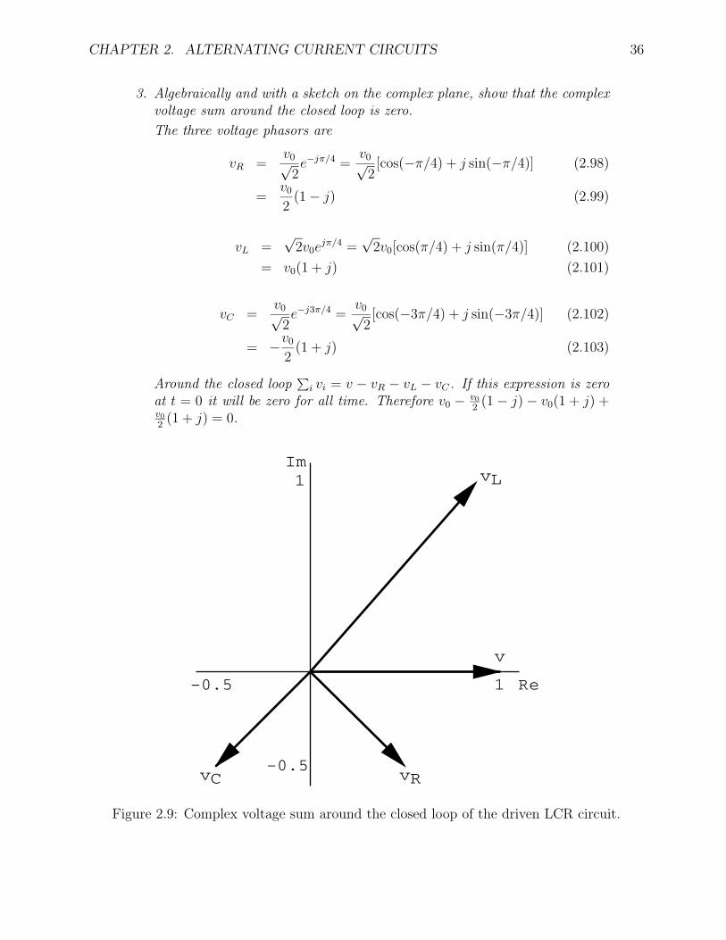
3. Algebraically and with a sketch on the complex plane, show that the complexvoltage sum around the closed loop is zero.
The three voltage phasors are
vR =v0√2e−jπ/4 =
v0√2[cos(−π/4) + j sin(−π/4)] (2.98)
=v0
2(1 − j) (2.99)
vL =√
2v0ejπ/4 =
√2v0[cos(π/4) + j sin(π/4)] (2.100)
= v0(1 + j) (2.101)
vC =v0√2e−j3π/4 =
v0√2[cos(−3π/4) + j sin(−3π/4)] (2.102)
= −v0
2(1 + j) (2.103)
Around the closed loop∑
i vi = v − vR − vL − vC. If this expression is zeroat t = 0 it will be zero for all time. Therefore v0 − v0
2(1 − j) − v0(1 + j) +
v0
2(1 + j) = 0.
vC vR
vL
v
Im
Re
1
1
−0.5
−0.5
Figure 2.9: Complex voltage sum around the closed loop of the driven LCR circuit.
CHAPTER 2. ALTERNATING CURRENT CIRCUITS 37
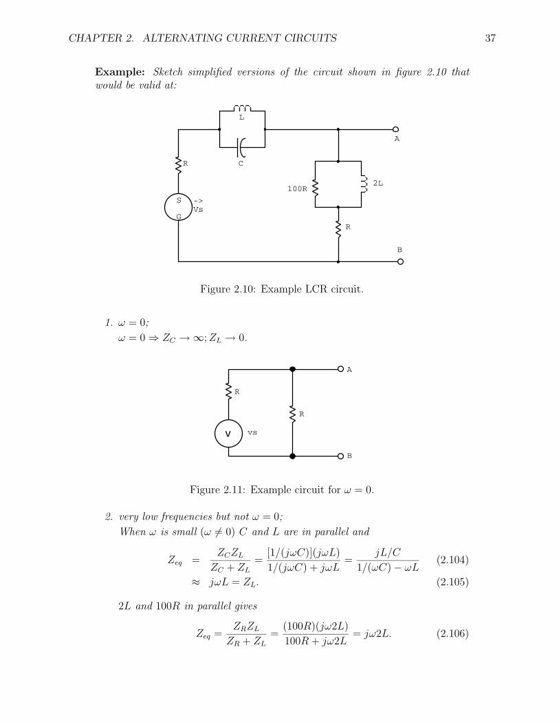
Example: Sketch simplified versions of the circuit shown in figure 2.10 thatwould be valid at:
B
A
->Vs
R
2L100R
C
L
R
S
G
Figure 2.10: Example LCR circuit.
1. ω = 0;
ω = 0 ⇒ ZC → ∞; ZL → 0.
vs
R
R
B
A
v
Figure 2.11: Example circuit for ω = 0.
2. very low frequencies but not ω = 0;
When ω is small (ω = 0) C and L are in parallel and
Zeq =ZCZL
ZC + ZL
=[1/(jωC)](jωL)
1/(jωC) + jωL=
jL/C
1/(ωC) − ωL(2.104)
≈ jωL = ZL. (2.105)
2L and 100R in parallel gives
Zeq =ZRZL
ZR + ZL
=(100R)(jω2L)
100R + jω2L= jω2L. (2.106)
CHAPTER 2. ALTERNATING CURRENT CIRCUITS 38
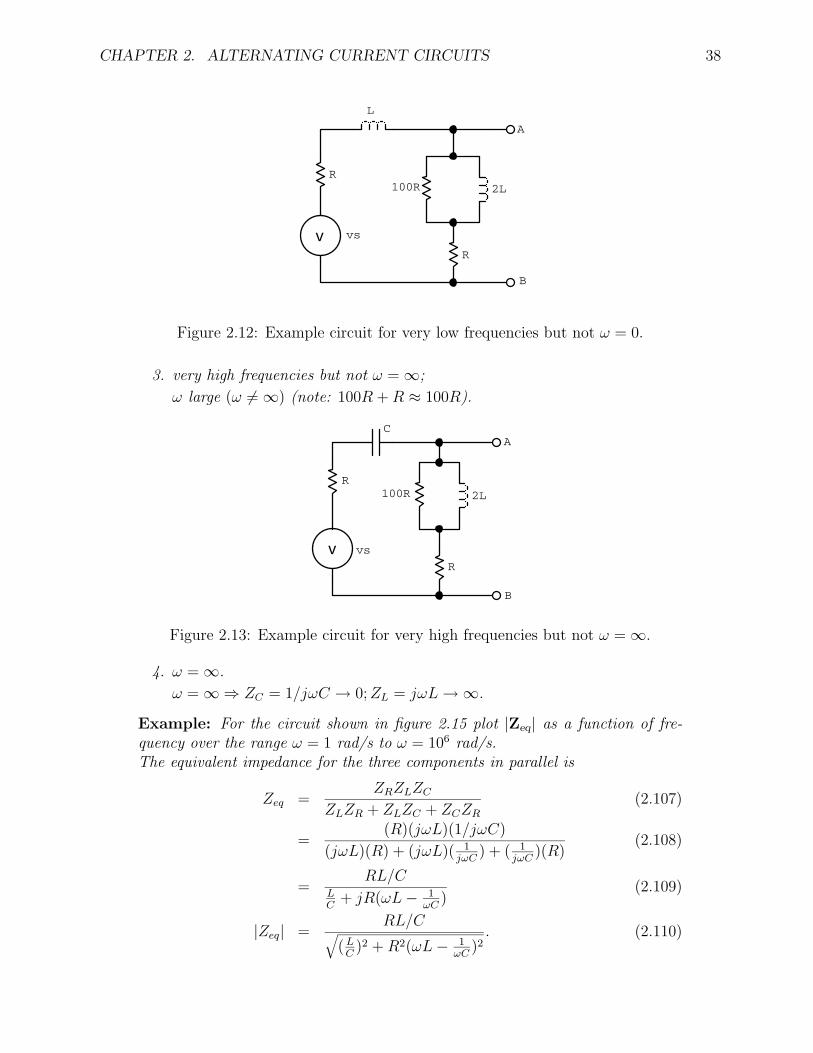
L
R2L100R
vs
R
B
A
v
Figure 2.12: Example circuit for very low frequencies but not ω = 0.
3. very high frequencies but not ω = ∞;
ω large (ω = ∞) (note: 100R + R ≈ 100R).
R
vs
R100R 2L
C
B
A
v
Figure 2.13: Example circuit for very high frequencies but not ω = ∞.
4. ω = ∞.
ω = ∞ ⇒ ZC = 1/jωC → 0; ZL = jωL → ∞.
Example: For the circuit shown in figure 2.15 plot |Zeq| as a function of fre-quency over the range ω = 1 rad/s to ω = 106 rad/s.The equivalent impedance for the three components in parallel is
Zeq =ZRZLZC
ZLZR + ZLZC + ZCZR
(2.107)
=(R)(jωL)(1/jωC)
(jωL)(R) + (jωL)( 1jωC
) + ( 1jωC
)(R)(2.108)
=RL/C
LC
+ jR(ωL − 1ωC
)(2.109)
|Zeq| =RL/C√
(LC
)2 + R2(ωL − 1ωC
)2. (2.110)
CHAPTER 2. ALTERNATING CURRENT CIRCUITS 39
vs R
R 100R
B
A
v
Figure 2.14: Example circuit for ω = ∞.
0.1microF10H1kohm
Figure 2.15: Example circuit with components in parallel.
Plugging in the numerical values gives
|Zeq| =103 × 10 × 107√
( 1010−7 )2 + 106(10ω − 107
ω)2
(2.111)
=1011√
1016 + 108(ω − 106
ω)2
(2.112)
=107√
108 + (ω − 106
ω)2
. (2.113)
A table of values and its plot follows.
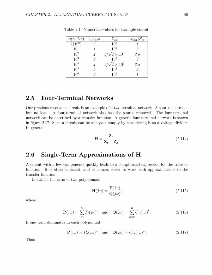
CHAPTER 2. ALTERNATING CURRENT CIRCUITS 40
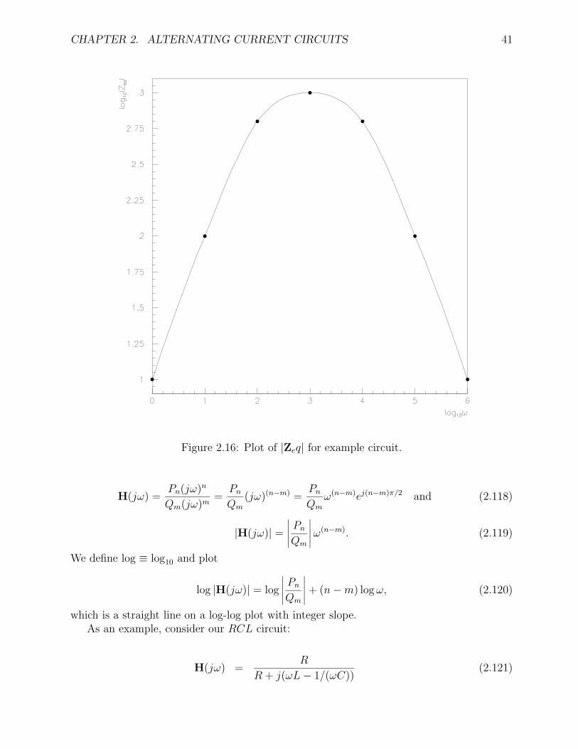
Table 2.1: Numerical values for example circuit.
ω(rad/s) log10 ω |Zeq| log10 |Zeq|1(100) 0 101 1101 1 102 2
102 2 1/√
2 × 10³ 2.8103 3 103 3
104 4 1/√
2 × 10³ 2.8105 5 102 2106 6 101 1
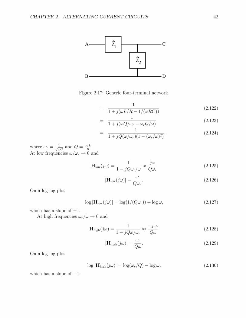
2.5 Four-Terminal Networks
Our previous resonance circuit is an example of a two-terminal network. A source is presentbut no load. A four-terminal network also has the source removed. The four-terminalnetwork can be described by a transfer function. A generic four-terminal network is shownin figure 2.17. Such a circuit can be analyzed simply by considering it as a voltage divider.In general
H =Z2
Z1 + Z2
. (2.114)
2.6 Single-Term Approximations of H
A circuit with a few components quickly leads to a complicated expression for the transferfunction. It is often sufficient, and of course, easier to work with approximations to thetransfer function.
Let H be the ratio of two polynomials
H(jω) =P(jω)
Q(jω), (2.115)
where
P(jω) =N∑
i=0
Pi(jω)i and Q(jω) =M∑
k=0
Qk(jω)k. (2.116)
If one term dominates in each polynomial
P(jω) ≈ Pn(jω)n and Q(jω) ≈ Qm(jω)m. (2.117)
Thus
CHAPTER 2. ALTERNATING CURRENT CIRCUITS 41
Figure 2.16: Plot of |Zeq| for example circuit.
H(jω) =Pn(jω)n
Qm(jω)m=
Pn
Qm
(jω)(n−m) =Pn
Qm
ω(n−m)ej(n−m)π/2 and (2.118)
|H(jω)| =
∣∣∣∣∣ Pn
Qm
∣∣∣∣∣ω(n−m). (2.119)
We define log ≡ log10 and plot
log |H(jω)| = log
∣∣∣∣∣ Pn
Qm
∣∣∣∣∣+ (n − m) log ω, (2.120)
which is a straight line on a log-log plot with integer slope.As an example, consider our RCL circuit:
H(jω) =R
R + j(ωL − 1/(ωC))(2.121)
CHAPTER 2. ALTERNATING CURRENT CIRCUITS 42
Z1
Z2
B
A
D
C
Figure 2.17: Generic four-terminal network.
=1
1 + j(ωL/R − 1/(ωRC))(2.122)
=1
1 + j(ωQ/ωr − ωrQ/ω)(2.123)
=1
1 + jQ(ω/ωr)(1 − (ωr/ω)2), (2.124)
where ωr = 1√LC
and Q = ωrLR
.
At low frequencies ω/ωr → 0 and
Hlow(jω) =1
1 − jQωr/ω≈ jω
Qωr
(2.125)
|Hlow(jω)| =ω
Qωr
. (2.126)
On a log-log plot
log |Hlow(jω)| = log(1/(Qωr)) + log ω, (2.127)
which has a slope of +1.At high frequencies ωr/ω → 0 and
Hhigh(jω) =1
1 + jQω/ωr
≈ −jωr
Qω(2.128)
|Hhigh(jω)| =ωr
Qω. (2.129)
On a log-log plot
log |Hhigh(jω)| = log(ωr/Q) − log ω, (2.130)
which has a slope of −1.
CHAPTER 2. ALTERNATING CURRENT CIRCUITS 43
2.7 Problems
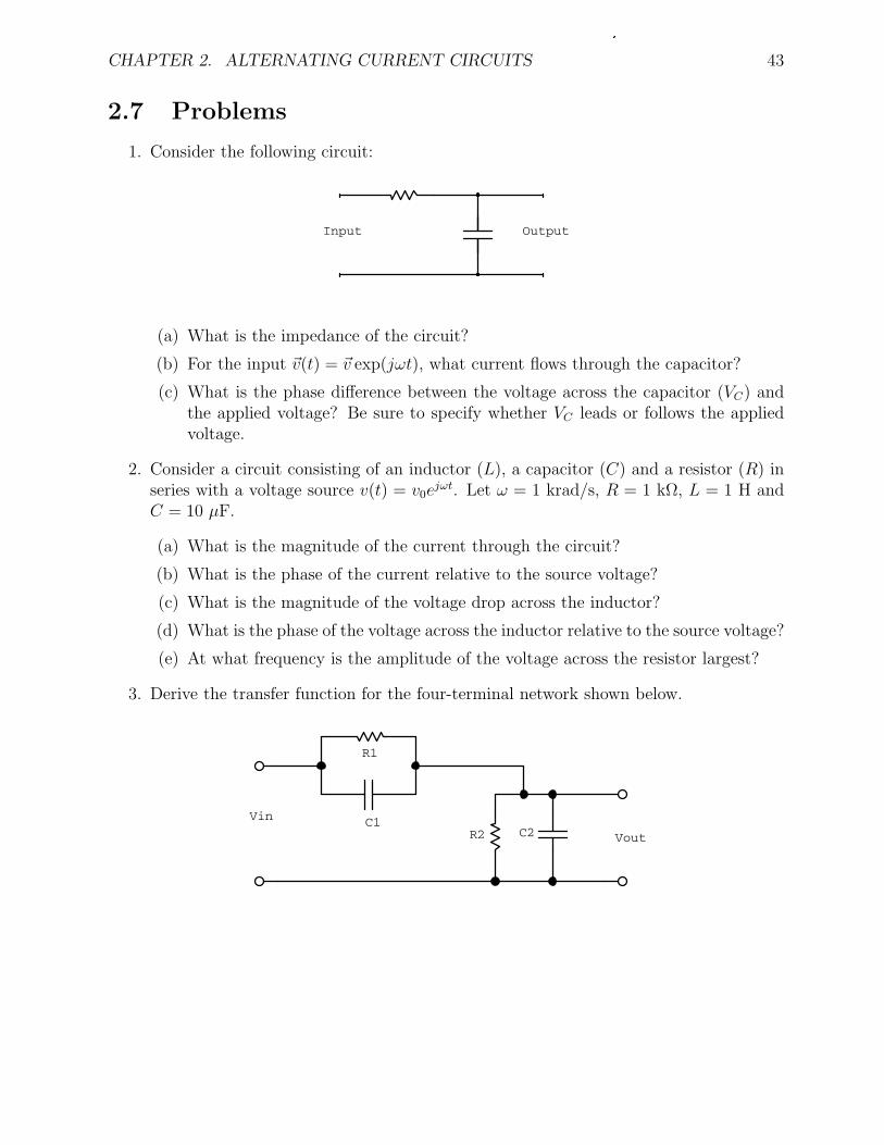
1. Consider the following circuit:
OutputInput
(a) What is the impedance of the circuit?
(b) For the input v(t) = v exp(jωt), what current flows through the capacitor?
(c) What is the phase difference between the voltage across the capacitor (VC) andthe applied voltage? Be sure to specify whether VC leads or follows the appliedvoltage.
2. Consider a circuit consisting of an inductor (L), a capacitor (C) and a resistor (R) inseries with a voltage source v(t) = v0e
jωt. Let ω = 1 krad/s, R = 1 kΩ, L = 1 H andC = 10 µF.
(a) What is the magnitude of the current through the circuit?
(b) What is the phase of the current relative to the source voltage?
(c) What is the magnitude of the voltage drop across the inductor?
(d) What is the phase of the voltage across the inductor relative to the source voltage?
(e) At what frequency is the amplitude of the voltage across the resistor largest?
3. Derive the transfer function for the four-terminal network shown below.
C2R2C1
R1
Vout
Vin
Chapter 3
Filter Circuits
Lets now apply our knowledge of AC circuits to some practical applications. We will firstlook at some simple passive filters (skipping active filters) and then an amplifier model.Again we will rely on complex variables.
3.1 Filters and Amplifiers
Simplistically, filters and amplifiers can be considered as four-terminal networks describedby a transfer function as follows:
vout(jω) = H(jω)vin(jω). (3.1)
Figure 3.1 shows some ideal transfer functions. If H(jω) = H ≡ A is a real constantthen we call the network an ideal amplifier. If H(jω) = Θ(j(ω − ω0)) is a heavyside stepfunction we refer to the circuit as an ideal low-pass filter, and if H(jω) = 1 − Θ(j(ω − ω0))an ideal high-pass filter.
3.2 Log-Log Plots and Decibels
A log-log plot of a circuit’s transfer function can be a useful qualitative tool to allow us tounderstand most of the important features of filter and amplifier circuits. The commonlyused decibel unit will be defined. Although unappealing to the physicist this unit is still inwide spread use in electronics. Lets start.
If P1 and P2 are two powers, we define the decibel as
dB ≡ 10 logP2
P1
= 10 logV 2
2
V 21
= 20 log∣∣∣∣V2
V1
∣∣∣∣ . (3.2)
where we have used P ∝ V 2.The decibel is a property of the network and not the signals. Hence we can make
use of any convenient signals in defining decibel. If two constant equal amplitude sources,|vin(jω1)| = |vin(jω2)|, are applied to a four-terminal network we may write
44
CHAPTER 3. FILTER CIRCUITS 45
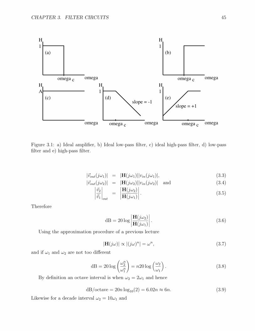
H1
omegaomega c
(a)
H1
omegaomega c
(b)
HA
omega
(c)
H1
omegaomega c
slope = -1(d)
H1
omegaomega c
slope = +1
(e)
Figure 3.1: a) Ideal amplifier, b) Ideal low-pass filter, c) ideal high-pass filter, d) low-passfilter and e) high-pass filter.
|vout(jω1)| = |H(jω1)||vin(jω1)|, (3.3)
|vout(jω2)| = |H(jω2)||vin(jω2)| and (3.4)∣∣∣∣∣v2
v1
∣∣∣∣∣out
=
∣∣∣∣∣H(jω2)
H(jω1)
∣∣∣∣∣ . (3.5)
Therefore
dB = 20 log
∣∣∣∣∣H(jω2)
H(jω1)
∣∣∣∣∣ . (3.6)
Using the approximation procedure of a previous lecture
|H(jω)| ∝ |(jω)n| = ωn, (3.7)
and if ω1 and ω2 are not too different
dB = 20 log
(ωn
2
ωn1
)= n20 log
(ω2
ω1
). (3.8)
By definition an octave interval is when ω2 = 2ω1 and hence
dB/octave = 20n log10(2) = 6.02n ≈ 6n. (3.9)
Likewise for a decade interval ω2 = 10ω1 and
CHAPTER 3. FILTER CIRCUITS 46
dB/decade = 20n log10(10) = 20n. (3.10)
3.3 Passive RC Filters
We will now use our passive circuit elements to design some filter circuits. Inductors are notvery good devices and hence we will concentrate on the use of resistors and capacitors.
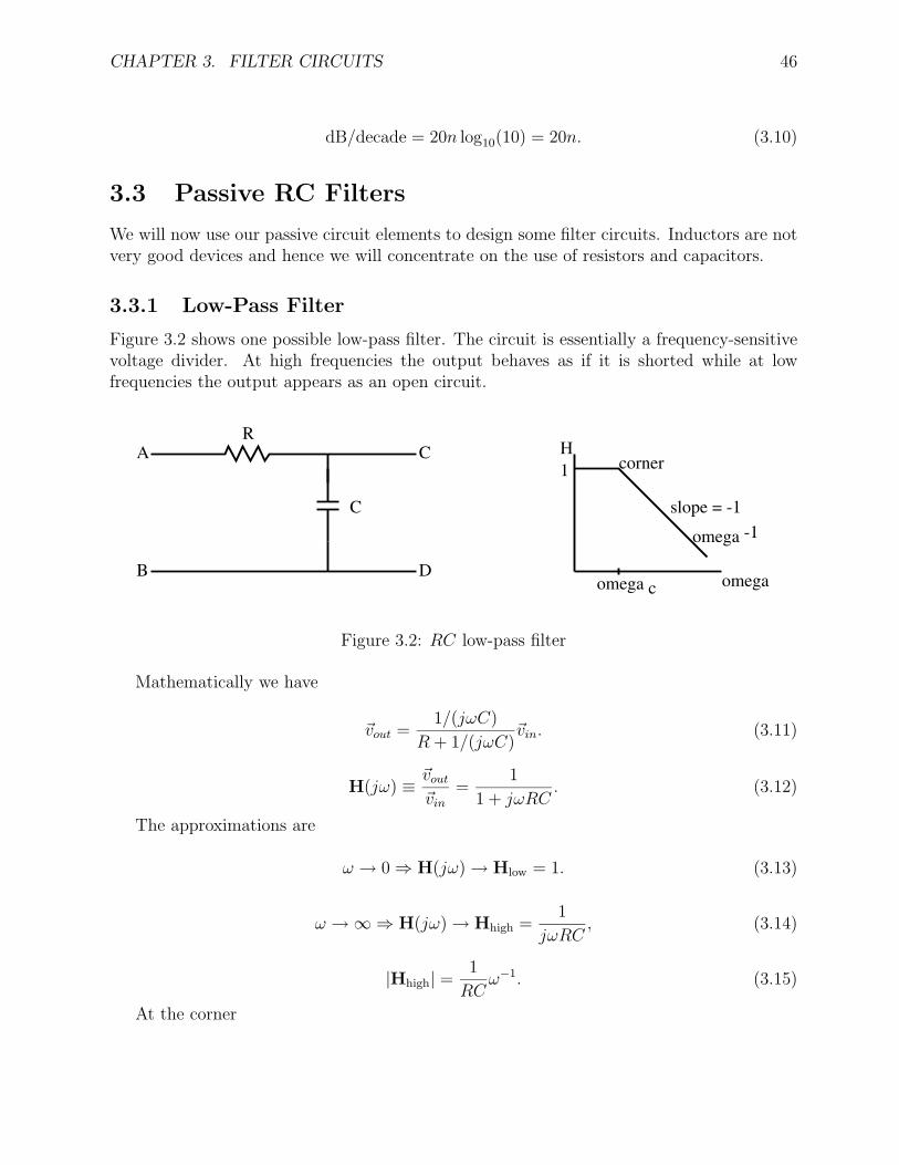
3.3.1 Low-Pass Filter
Figure 3.2 shows one possible low-pass filter. The circuit is essentially a frequency-sensitivevoltage divider. At high frequencies the output behaves as if it is shorted while at lowfrequencies the output appears as an open circuit.
R
C
B
A
D
C H1
omega c omega
omega -1
corner
slope = -1
Figure 3.2: RC low-pass filter
Mathematically we have
vout =1/(jωC)
R + 1/(jωC)vin. (3.11)
H(jω) ≡ vout
vin
=1
1 + jωRC. (3.12)
The approximations are
ω → 0 ⇒ H(jω) → Hlow = 1. (3.13)
ω → ∞ ⇒ H(jω) → Hhigh =1
jωRC, (3.14)
|Hhigh| =1
RCω−1. (3.15)
At the corner
CHAPTER 3. FILTER CIRCUITS 47
|Hhigh| = |Hlow| ⇒ 1
RCωc
= 1. (3.16)
Therefore
ωc =1
RC(3.17)
is the corner frequency of the filter. At the corner frequency
H(jωc) =1
1 + jωcRC=
1
1 + j=
1 − j
2, (3.18)
|H(jωc)| =1√2. (3.19)
We say that the output is down by 1/√
2 at the corner frequency.
3.3.2 Approximate Integrater
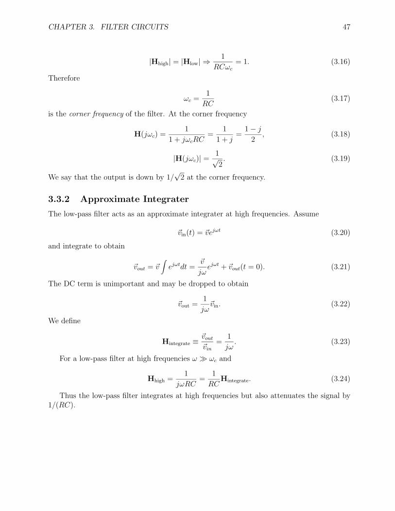
The low-pass filter acts as an approximate integrater at high frequencies. Assume
vin(t) = vejωt (3.20)
and integrate to obtain
vout = v∫
ejωtdt =v
jωejωt + vout(t = 0). (3.21)
The DC term is unimportant and may be dropped to obtain
vout =1
jωvin. (3.22)
We define
Hintegrate ≡ vout
vin
=1
jω. (3.23)
For a low-pass filter at high frequencies ω ωc and
Hhigh =1
jωRC=
1
RCHintegrate. (3.24)
Thus the low-pass filter integrates at high frequencies but also attenuates the signal by1/(RC).
CHAPTER 3. FILTER CIRCUITS 48
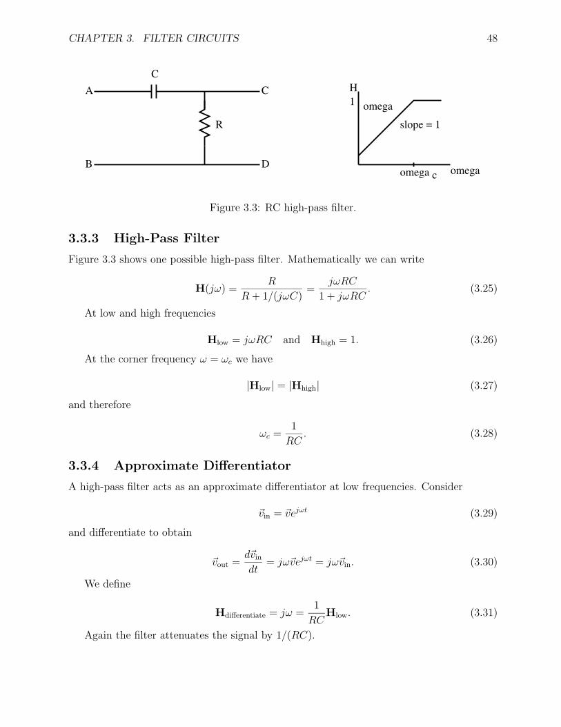
C
R
B
A
D
C H1
omega c omega
omega
slope = 1
Figure 3.3: RC high-pass filter.
3.3.3 High-Pass Filter
Figure 3.3 shows one possible high-pass filter. Mathematically we can write
H(jω) =R
R + 1/(jωC)=
jωRC
1 + jωRC. (3.25)
At low and high frequencies
Hlow = jωRC and Hhigh = 1. (3.26)
At the corner frequency ω = ωc we have
|Hlow| = |Hhigh| (3.27)
and therefore
ωc =1
RC. (3.28)
3.3.4 Approximate Differentiator
A high-pass filter acts as an approximate differentiator at low frequencies. Consider
vin = vejωt (3.29)
and differentiate to obtain
vout =dvin
dt= jωvejωt = jωvin. (3.30)
We define
Hdifferentiate = jω =1
RCHlow. (3.31)
Again the filter attenuates the signal by 1/(RC).
CHAPTER 3. FILTER CIRCUITS 49
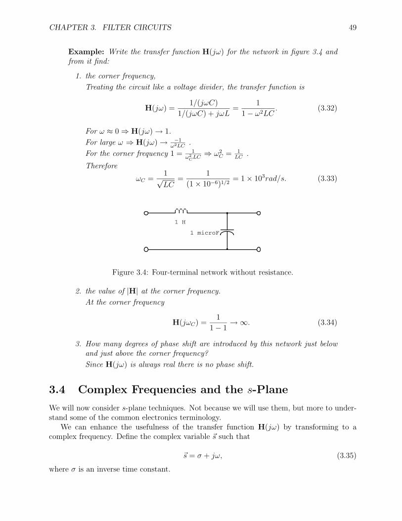
Example: Write the transfer function H(jω) for the network in figure 3.4 andfrom it find:
1. the corner frequency,
Treating the circuit like a voltage divider, the transfer function is
H(jω) =1/(jωC)
1/(jωC) + jωL=
1
1 − ω2LC. (3.32)
For ω ≈ 0 ⇒ H(jω) → 1.
For large ω ⇒ H(jω) → −1ω2LC
.
For the corner frequency 1 = 1ω2
CLC⇒ ω2
C = 1LC
.
Therefore
ωC =1√LC
=1
(1 × 10⁻⁶)1/2= 1 × 10³rad/s. (3.33)
1 microF
1 H
Figure 3.4: Four-terminal network without resistance.
2. the value of |H| at the corner frequency.
At the corner frequency
H(jωC) =1
1 − 1→ ∞. (3.34)
3. How many degrees of phase shift are introduced by this network just belowand just above the corner frequency?
Since H(jω) is always real there is no phase shift.
3.4 Complex Frequencies and the s-Plane
We will now consider s-plane techniques. Not because we will use them, but more to under-stand some of the common electronics terminology.
We can enhance the usefulness of the transfer function H(jω) by transforming to acomplex frequency. Define the complex variable s such that
s = σ + jω, (3.35)
where σ is an inverse time constant.
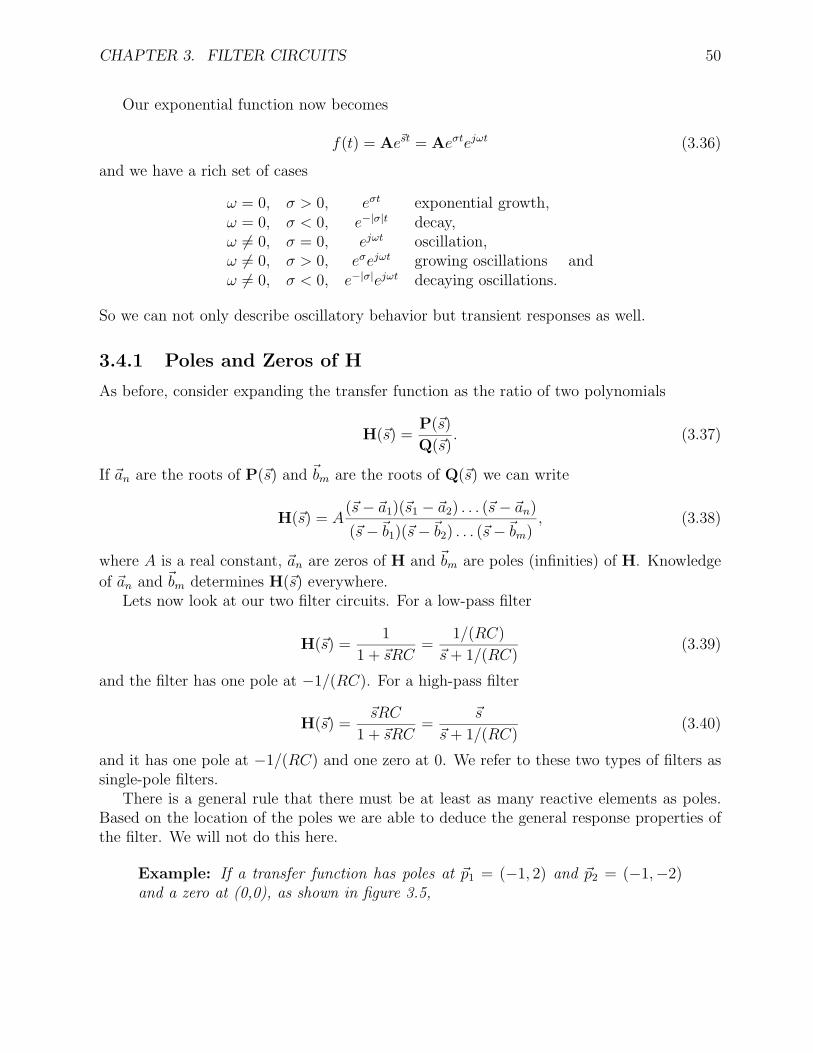
CHAPTER 3. FILTER CIRCUITS 50
Our exponential function now becomes
f(t) = Aest = Aeσtejωt (3.36)
and we have a rich set of cases
ω = 0, σ > 0, eσt exponential growth,ω = 0, σ < 0, e−|σ|t decay,ω = 0, σ = 0, ejωt oscillation,ω = 0, σ > 0, eσejωt growing oscillations andω = 0, σ < 0, e−|σ|ejωt decaying oscillations.
So we can not only describe oscillatory behavior but transient responses as well.
3.4.1 Poles and Zeros of H
As before, consider expanding the transfer function as the ratio of two polynomials
H(s) =P(s)
Q(s). (3.37)
If an are the roots of P(s) and bm are the roots of Q(s) we can write
H(s) = A(s − a1)(s1 − a2) . . . (s − an)
(s −b1)(s −b2) . . . (s −bm), (3.38)
where A is a real constant, an are zeros of H and bm are poles (infinities) of H. Knowledge
of an and bm determines H(s) everywhere.Lets now look at our two filter circuits. For a low-pass filter
H(s) =1
1 + sRC=
1/(RC)
s + 1/(RC)(3.39)
and the filter has one pole at −1/(RC). For a high-pass filter
H(s) =sRC
1 + sRC=
s
s + 1/(RC)(3.40)
and it has one pole at −1/(RC) and one zero at 0. We refer to these two types of filters assingle-pole filters.
There is a general rule that there must be at least as many reactive elements as poles.Based on the location of the poles we are able to deduce the general response properties ofthe filter. We will not do this here.
Example: If a transfer function has poles at p1 = (−1, 2) and p2 = (−1,−2)and a zero at (0,0), as shown in figure 3.5,
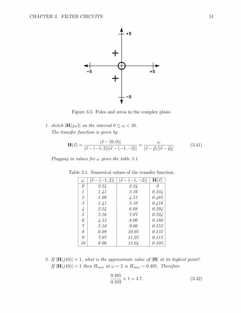
CHAPTER 3. FILTER CIRCUITS 51
+5
+5
−5
−5
Figure 3.5: Poles and zeros in the complex plane.
1. sketch |H(jω)| on the interval 0 ≤ ω < 10.
The transfer function is given by
H(s) =|s − (0, 0)|
|s − (−1, 2)||s − (−1,−2)| =ω
|s − p1||s − p2| (3.41)
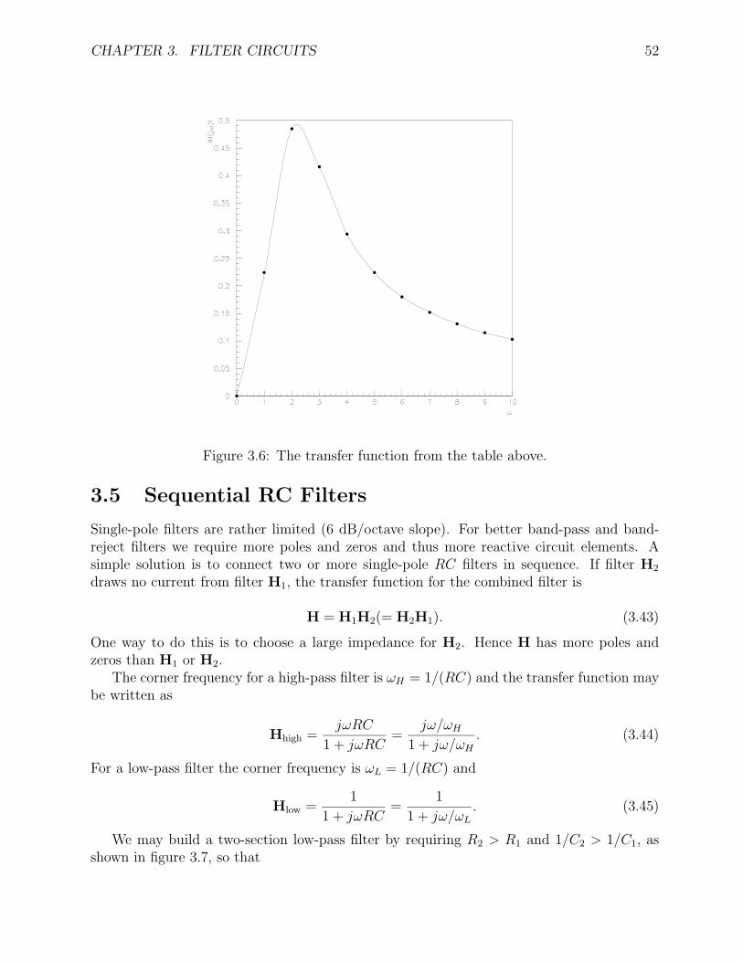
Plugging in values for ω gives the table 3.1.
Table 3.1: Numerical values of the transfer function.
ω |s − (−1, 2)| |s − (−1,−2)| H(s)0 2.24 2.24 01 1.41 3.16 0.2242 1.00 4.12 0.4853 1.41 5.10 0.4164 2.24 6.08 0.2945 3.16 7.07 0.2246 4.12 8.06 0.1807 5.10 9.06 0.1528 6.08 10.05 0.1319 7.07 11.05 0.11510 8.06 12.04 0.103
2. If |H(j10)| = 1, what is the approximate value of |H| at its highest point?
If |H(j10)| = 1 then Hmax at ω = 2 is Hmax = 0.485. Therefore
0.485
0.103× 1 = 4.7. (3.42)
CHAPTER 3. FILTER CIRCUITS 52
Figure 3.6: The transfer function from the table above.
3.5 Sequential RC Filters
Single-pole filters are rather limited (6 dB/octave slope). For better band-pass and band-reject filters we require more poles and zeros and thus more reactive circuit elements. Asimple solution is to connect two or more single-pole RC filters in sequence. If filter H2
draws no current from filter H1, the transfer function for the combined filter is
H = H1H2(= H2H1). (3.43)
One way to do this is to choose a large impedance for H2. Hence H has more poles andzeros than H1 or H2.
The corner frequency for a high-pass filter is ωH = 1/(RC) and the transfer function maybe written as
Hhigh =jωRC
1 + jωRC=
jω/ωH
1 + jω/ωH
. (3.44)
For a low-pass filter the corner frequency is ωL = 1/(RC) and
Hlow =1
1 + jωRC=
1
1 + jω/ωL
. (3.45)
We may build a two-section low-pass filter by requiring R2 > R1 and 1/C2 > 1/C1, asshown in figure 3.7, so that
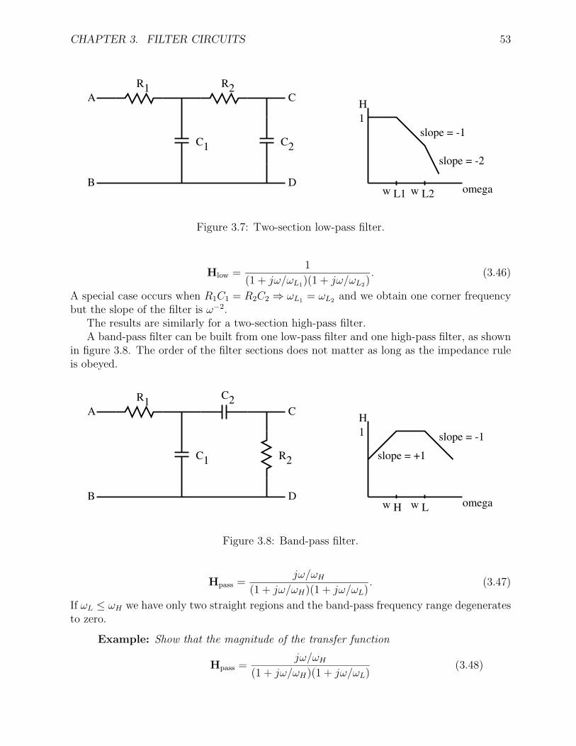
CHAPTER 3. FILTER CIRCUITS 53
C1 C2
R1 R2
B
A
D
CH1
w L1 w L2 omega
slope = -1
slope = -2
Figure 3.7: Two-section low-pass filter.
Hlow =1
(1 + jω/ωL1)(1 + jω/ωL2). (3.46)
A special case occurs when R1C1 = R2C2 ⇒ ωL1 = ωL2 and we obtain one corner frequencybut the slope of the filter is ω−2.
The results are similarly for a two-section high-pass filter.A band-pass filter can be built from one low-pass filter and one high-pass filter, as shown
in figure 3.8. The order of the filter sections does not matter as long as the impedance ruleis obeyed.
C1 R2
R1C2
B
A
D
CH1
w H w L omega
slope = +1
slope = -1
Figure 3.8: Band-pass filter.
Hpass =jω/ωH
(1 + jω/ωH)(1 + jω/ωL). (3.47)
If ωL ≤ ωH we have only two straight regions and the band-pass frequency range degeneratesto zero.
Example: Show that the magnitude of the transfer function
Hpass =jω/ωH
(1 + jω/ωH)(1 + jω/ωL)(3.48)
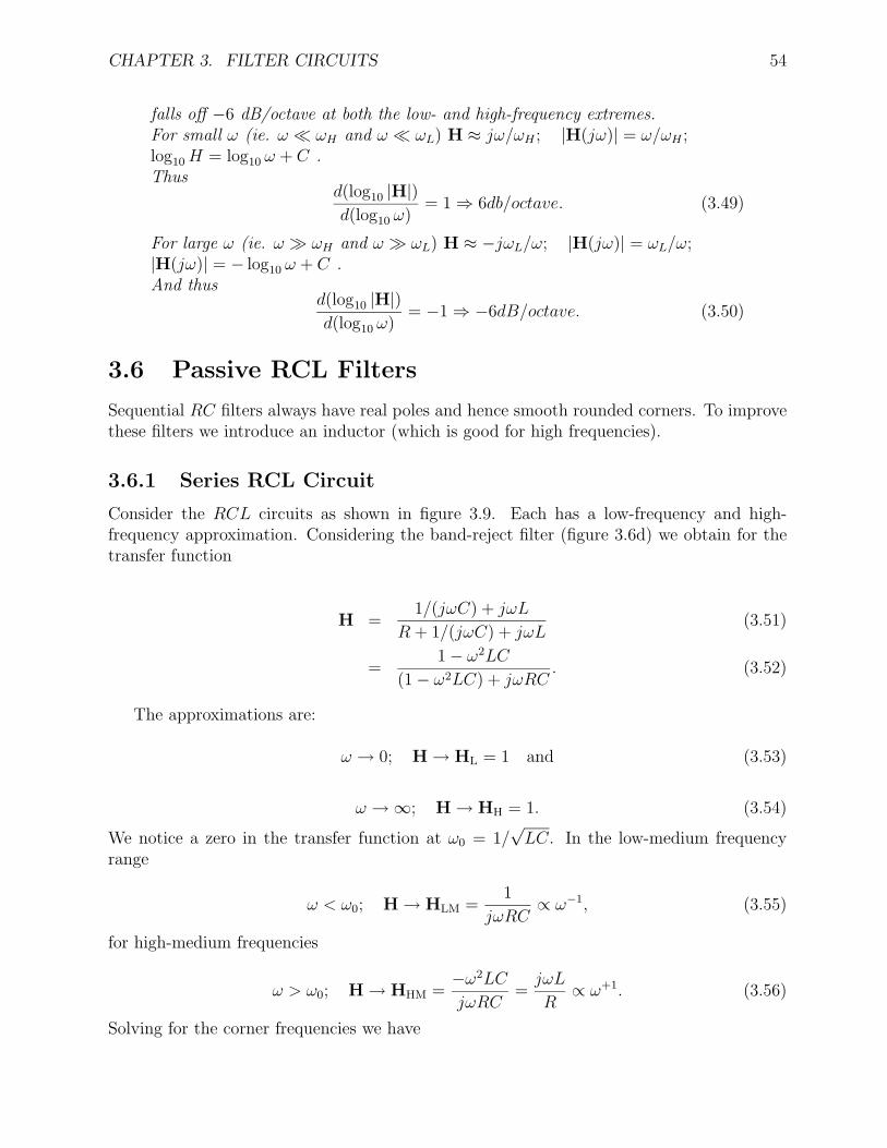
CHAPTER 3. FILTER CIRCUITS 54
falls off −6 dB/octave at both the low- and high-frequency extremes.For small ω (ie. ω ωH and ω ωL) H ≈ jω/ωH ; |H(jω)| = ω/ωH ;log10 H = log10 ω + C .Thus
d(log10 |H|)d(log10 ω)
= 1 ⇒ 6db/octave. (3.49)
For large ω (ie. ω ωH and ω ωL) H ≈ −jωL/ω; |H(jω)| = ωL/ω;|H(jω)| = − log10 ω + C .And thus
d(log10 |H|)d(log10 ω)
= −1 ⇒ −6dB/octave. (3.50)
3.6 Passive RCL Filters
Sequential RC filters always have real poles and hence smooth rounded corners. To improvethese filters we introduce an inductor (which is good for high frequencies).
3.6.1 Series RCL Circuit
Consider the RCL circuits as shown in figure 3.9. Each has a low-frequency and high-frequency approximation. Considering the band-reject filter (figure 3.6d) we obtain for thetransfer function
H =1/(jωC) + jωL
R + 1/(jωC) + jωL(3.51)
=1 − ω2LC
(1 − ω2LC) + jωRC. (3.52)
The approximations are:
ω → 0; H → HL = 1 and (3.53)
ω → ∞; H → HH = 1. (3.54)
We notice a zero in the transfer function at ω0 = 1/√
LC. In the low-medium frequencyrange
ω < ω0; H → HLM =1
jωRC∝ ω−1, (3.55)
for high-medium frequencies
ω > ω0; H → HHM =−ω2LC
jωRC=
jωL
R∝ ω+1. (3.56)
Solving for the corner frequencies we have
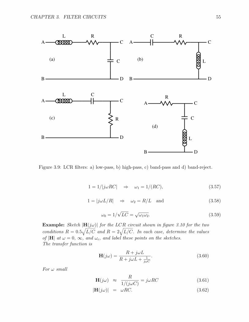
CHAPTER 3. FILTER CIRCUITS 55
(a)
L R
C
B
A
D
C
(b)
C R
L
B
A
D
C
(c)
L C
R
B
A
D
C
(d)
R
L
C
B
A
D
C
Figure 3.9: LCR filters: a) low-pass, b) high-pass, c) band-pass and d) band-reject.
1 = 1/|jωRC| ⇒ ω1 = 1/(RC), (3.57)
1 = |jωL/R| ⇒ ω2 = R/L and (3.58)
ω0 = 1/√
LC =√
ω1ω2. (3.59)
Example: Sketch |H(jω)| for the LCR circuit shown in figure 3.10 for the two
conditions R = 0.5√
L/C and R = 2√
L/C. In each case, determine the values
of |H| at ω = 0, ∞, and ωc, and label these points on the sketches.The transfer function is
H(jω) =R + jωL
R + jωL + 1jωC
. (3.60)
For ω small
H(jω) ≈ R
1/(jωC)= jωRC (3.61)
|H(jω)| = ωRC. (3.62)
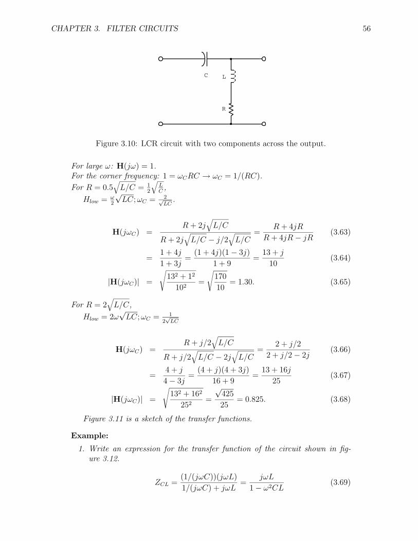
CHAPTER 3. FILTER CIRCUITS 56
R
LC
Figure 3.10: LCR circuit with two components across the output.
For large ω: H(jω) = 1.For the corner frequency: 1 = ωCRC → ωC = 1/(RC).
For R = 0.5√
L/C = 12
√LC,
Hlow = ω2
√LC; ωC = 2√
LC.
H(jωC) =R + 2j
√L/C
R + 2j√
L/C − j/2√
L/C=
R + 4jR
R + 4jR − jR(3.63)
=1 + 4j
1 + 3j=
(1 + 4j)(1 − 3j)
1 + 9=
13 + j
10(3.64)
|H(jωC)| =
√132 + 12
102=
√170
10= 1.30. (3.65)
For R = 2√
L/C,
Hlow = 2ω√
LC; ωC = 12√
LC
H(jωC) =R + j/2
√L/C
R + j/2√
L/C − 2j√
L/C=
2 + j/2
2 + j/2 − 2j(3.66)
=4 + j
4 − 3j=
(4 + j)(4 + 3j)
16 + 9=
13 + 16j
25(3.67)
|H(jωC)| =
√132 + 162
252=
√425
25= 0.825. (3.68)
Figure 3.11 is a sketch of the transfer functions.
Example:
1. Write an expression for the transfer function of the circuit shown in fig-ure 3.12.
ZCL =(1/(jωC))(jωL)
1/(jωC) + jωL=
jωL
1 − ω2CL(3.69)
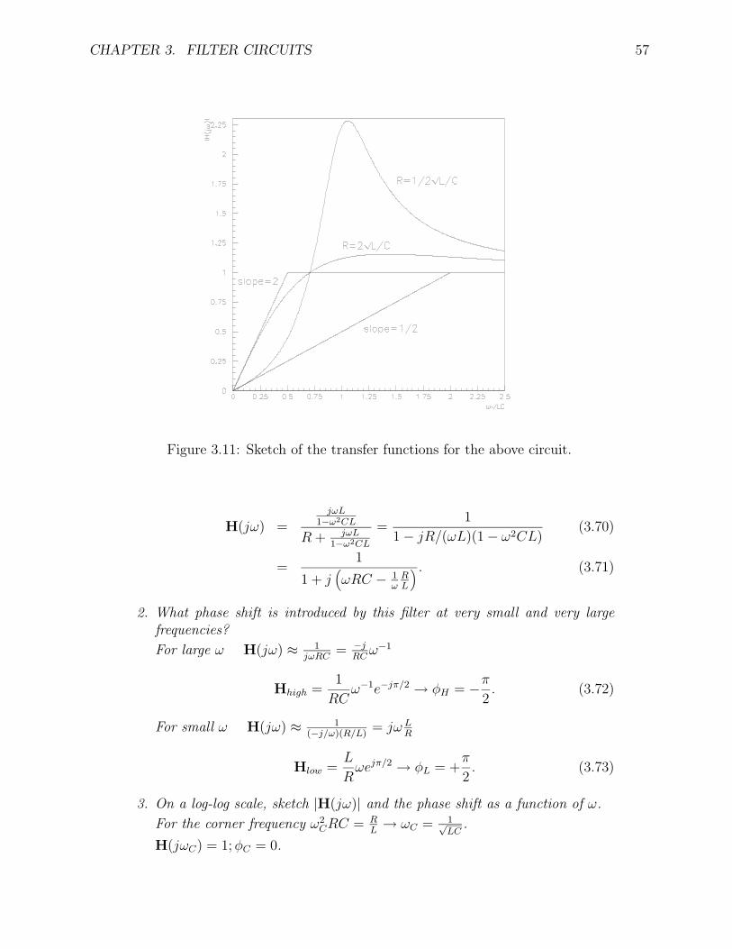
CHAPTER 3. FILTER CIRCUITS 57
Figure 3.11: Sketch of the transfer functions for the above circuit.
H(jω) =jωL
1−ω2CL
R + jωL1−ω2CL
=1
1 − jR/(ωL)(1 − ω2CL)(3.70)
=1
1 + j(ωRC − 1
ωRL
) . (3.71)
2. What phase shift is introduced by this filter at very small and very largefrequencies?
For large ω H(jω) ≈ 1jωRC
= −jRC
ω−1
Hhigh =1
RCω−1e−jπ/2 → φH = −π
2. (3.72)
For small ω H(jω) ≈ 1(−j/ω)(R/L)
= jω LR
Hlow =L
Rωejπ/2 → φL = +
π
2. (3.73)
3. On a log-log scale, sketch |H(jω)| and the phase shift as a function of ω.
For the corner frequency ω2CRC = R
L→ ωC = 1√
LC.
H(jωC) = 1; φC = 0.
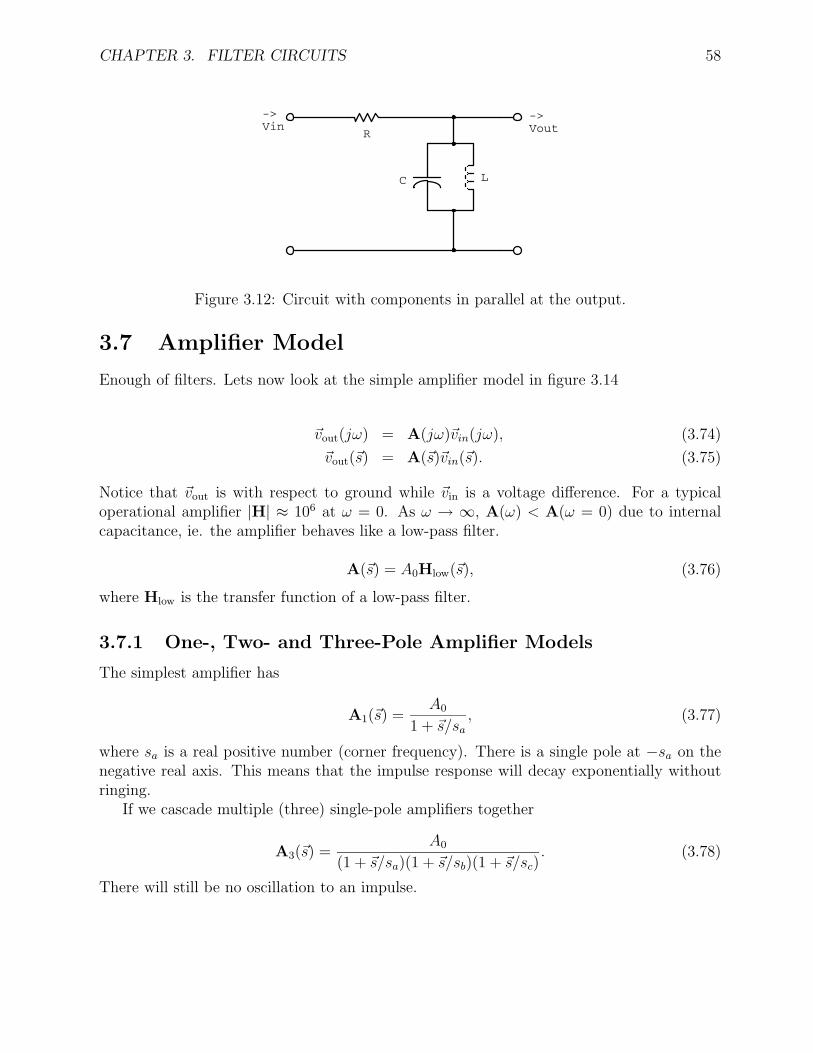
CHAPTER 3. FILTER CIRCUITS 58
->Vin
->VoutR
LC
Figure 3.12: Circuit with components in parallel at the output.
3.7 Amplifier Model
Enough of filters. Lets now look at the simple amplifier model in figure 3.14
vout(jω) = A(jω)vin(jω), (3.74)
vout(s) = A(s)vin(s). (3.75)
Notice that vout is with respect to ground while vin is a voltage difference. For a typicaloperational amplifier |H| ≈ 106 at ω = 0. As ω → ∞, A(ω) < A(ω = 0) due to internalcapacitance, ie. the amplifier behaves like a low-pass filter.
A(s) = A0Hlow(s), (3.76)
where Hlow is the transfer function of a low-pass filter.
3.7.1 One-, Two- and Three-Pole Amplifier Models
The simplest amplifier has
A1(s) =A0
1 + s/sa
, (3.77)
where sa is a real positive number (corner frequency). There is a single pole at −sa on thenegative real axis. This means that the impulse response will decay exponentially withoutringing.
If we cascade multiple (three) single-pole amplifiers together
A3(s) =A0
(1 + s/sa)(1 + s/sb)(1 + s/sc). (3.78)
There will still be no oscillation to an impulse.
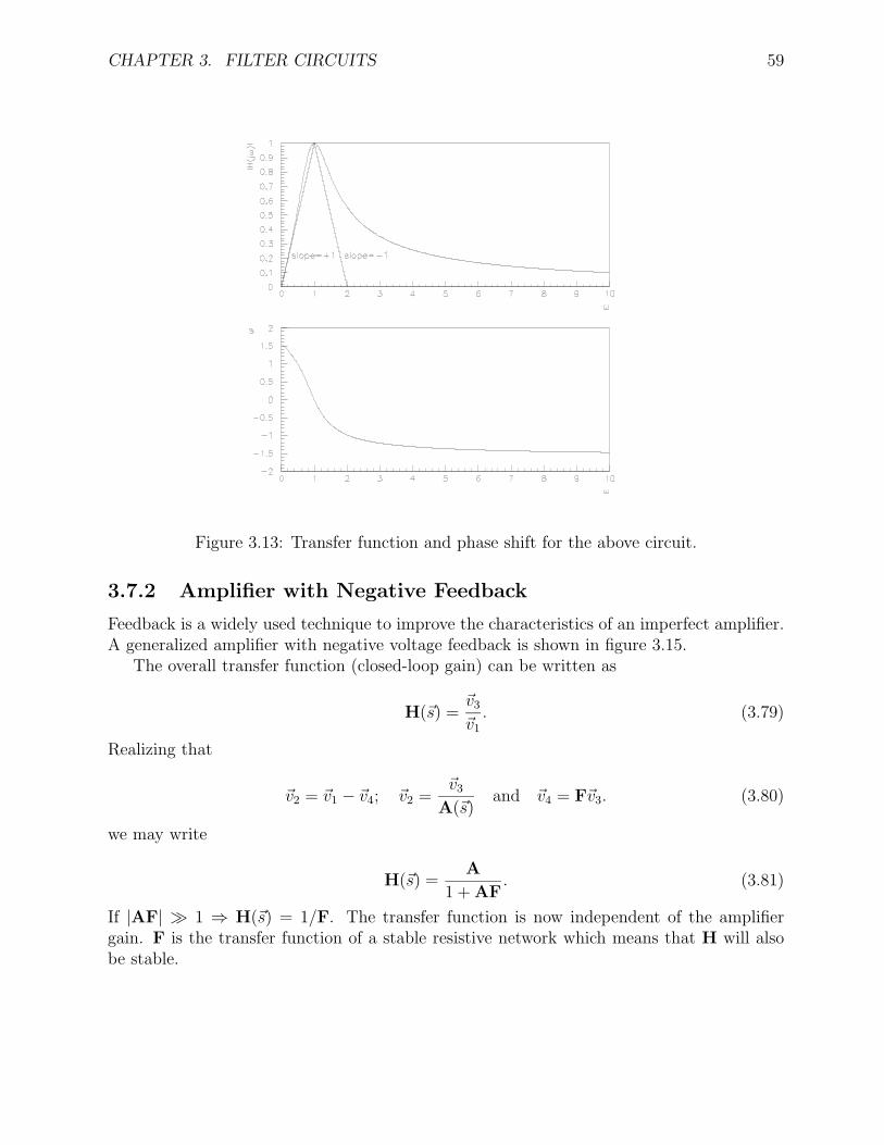
CHAPTER 3. FILTER CIRCUITS 59
Figure 3.13: Transfer function and phase shift for the above circuit.
3.7.2 Amplifier with Negative Feedback
Feedback is a widely used technique to improve the characteristics of an imperfect amplifier.A generalized amplifier with negative voltage feedback is shown in figure 3.15.
The overall transfer function (closed-loop gain) can be written as
H(s) =v3
v1
. (3.79)
Realizing that
v2 = v1 − v4; v2 =v3
A(s)and v4 = Fv3. (3.80)
we may write
H(s) =A
1 + AF. (3.81)
If |AF| 1 ⇒ H(s) = 1/F. The transfer function is now independent of the amplifiergain. F is the transfer function of a stable resistive network which means that H will alsobe stable.
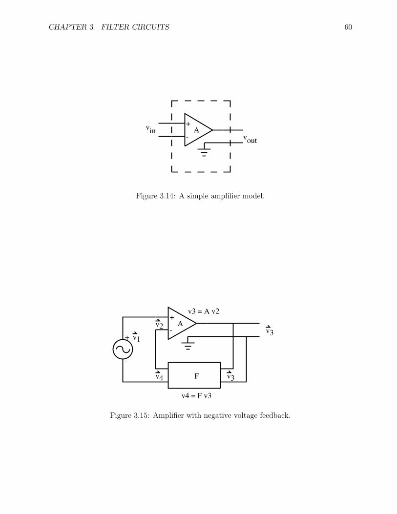
CHAPTER 3. FILTER CIRCUITS 60
A-
+vinvout
Figure 3.14: A simple amplifier model.
A-
+v2
v1+
-
v3
v4 v3F
v4 = F v3
v3 = A v2
Figure 3.15: Amplifier with negative voltage feedback.
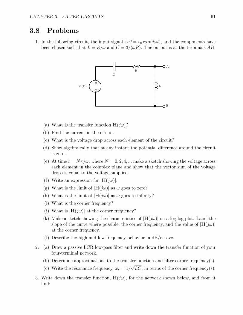
CHAPTER 3. FILTER CIRCUITS 61
3.8 Problems
1. In the following circuit, the input signal is v = v0 exp(jωt), and the components havebeen chosen such that L = R/ω and C = 3/(ωR). The output is at the terminals AB.
RC
Lv(t)
B
A
S
G
(a) What is the transfer function H(jω)?
(b) Find the current in the circuit.
(c) What is the voltage drop across each element of the circuit?
(d) Show algebraically that at any instant the potential difference around the circuitis zero.
(e) At time t = Nπ/ω, where N = 0, 2, 4, ... make a sketch showing the voltage acrosseach element in the complex plane and show that the vector sum of the voltagedrops is equal to the voltage supplied.
(f) Write an expression for |H(jω)|.(g) What is the limit of |H(jω)| as ω goes to zero?
(h) What is the limit of |H(jω)| as ω goes to infinity?
(i) What is the corner frequency?
(j) What is |H(jω)| at the corner frequency?
(k) Make a sketch showing the characteristics of |H(jω)| on a log-log plot. Label theslope of the curve where possible, the corner frequency, and the value of |H(jω)|at the corner frequency.
(l) Describe the high and low frequency behavior in dB/octave.
2. (a) Draw a passive LCR low-pass filter and write down the transfer function of yourfour-terminal network.
(b) Determine approximations to the transfer function and filter corner frequency(s).
(c) Write the resonance frequency, ωr = 1/√
LC, in terms of the corner frequency(s).
3. Write down the transfer function, H(jω), for the network shown below, and from itfind:
CHAPTER 3. FILTER CIRCUITS 62
(a) the corner frequency(s) and
(b) the value(s) of |H(jω)| at the corner frequency(s).
(c) Sketch |H(jω)| and the voltage phase-shift as a function of ω .
(d) What type of filter is this?
Vin VoutL
R
4. (a) What is the transfer function for the following circuit?
input outputCCC
RRR
(b) Describe the frequency response at low and high frequencies?
(c) Sketch the magnitude |H(jω)| on a log-log plot. (label slopes, the corner fre-quency(s), and |H(jωC)|)
(d) What is the signal attenuation for ω = 3(RC)−1.
5. (a) Show that the transfer function of a single-pole RC filter drops by 3 db at thecorner frequency. This is often refereed to as the 3 db down-point.
(b) Design a bandpass RC filter with the transfer function shown below. ω1 =103 rad/s and ω2 = 105 rad/s are the 3 db down-points of the RC filter sec-tions. Choose impedances so that the first section is not much affected by theloading of the second section.
(c) Are ω1 and ω2 the 3 db down-points of a bandpass filter?
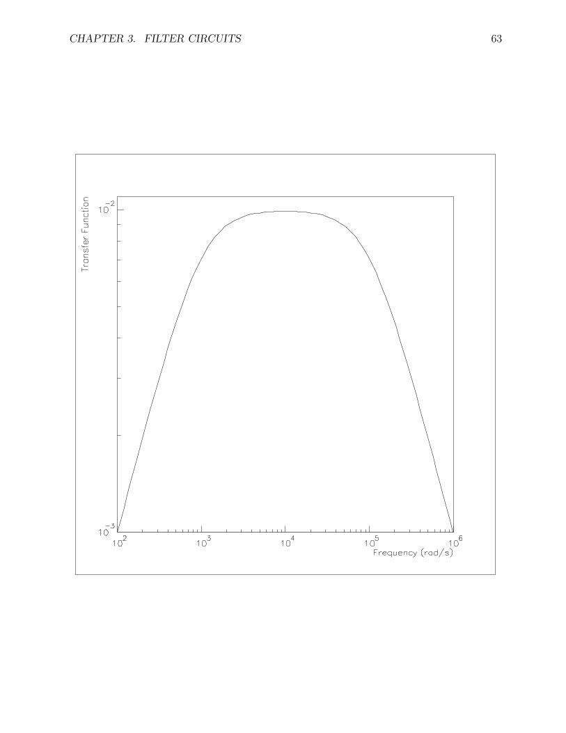
CHAPTER 3. FILTER CIRCUITS 63
Chapter 4
Diode Circuits
So far we have only considered passive circuit elements. Now we will consider our first reactivecircuit element, the diode. Hopefully things will start to get a little more interesting.
Along with the diode there is the transistor, which will be discussed in future lectures.These circuit elements are commonly made from a semiconductor basic material. Semicon-ductors along with the passive circuit elements are often integrated onto a single electronicschip. If a hundred or so transistors are on a chip it is referred to as an integrated circuit orIC. Large-scale integrated circuits, LSI, contain thousands of transistors. And today evenvery-large-scale integrated circuits, VLSI, exist, with hundreds of thousands of transistors.
Now lets talk physics.
4.1 Energy Levels
The physical principles of semiconductor devices can be understood by considering quantumenergy levels in the material. I will just give a sketchy view here and define some terminology.
Valance electrons are the electrons outside the closed shells of an atom. In silicon andgermanium there are four valence electrons, arsenic has five and gallium three. The largenumber of valance electrons favour these elements as semiconductors.
To sustain an electric current, a material must have charge carriers that are free to move.There is some probability that an atom may eject a valence electron which is then free tomove in the material. The conductivity of a material is thus a function of the number offree charge carriers per unit volume. Based on these probability densities it is common todivide materials into three categories: conductors, semiconductors and insulators.
In crystals atoms interact and bind by sharing valence electrons. The wave function isno longer associated with a single atom but extends over the entire crystal. One effect ofthe interaction between the atoms is that the otherwise degenerate energy levels split intoclosely spaced levels. Since the number of atoms is large, it is common to refer to this set oflevels as a continuous energy band.
In solid materials there usually exist a valance band which is an energy region wherethe states are filled or partially filled by valence electrons. The conduction band is definedto be the lowest unfilled energy band. So our three materials can be characterized bytheir band structure. An insulator has the valence and conduction band well separated. A
64
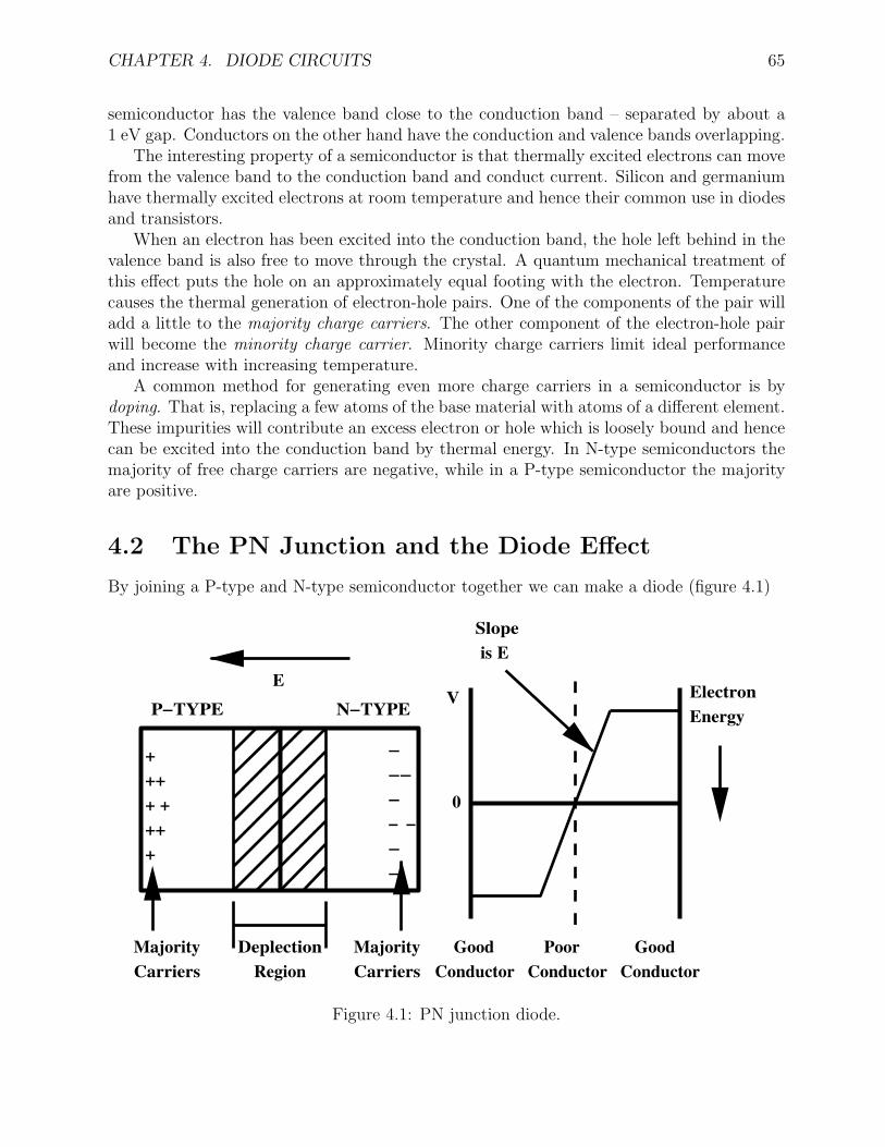
CHAPTER 4. DIODE CIRCUITS 65
semiconductor has the valence band close to the conduction band – separated by about a1 eV gap. Conductors on the other hand have the conduction and valence bands overlapping.
The interesting property of a semiconductor is that thermally excited electrons can movefrom the valence band to the conduction band and conduct current. Silicon and germaniumhave thermally excited electrons at room temperature and hence their common use in diodesand transistors.
When an electron has been excited into the conduction band, the hole left behind in thevalence band is also free to move through the crystal. A quantum mechanical treatment ofthis effect puts the hole on an approximately equal footing with the electron. Temperaturecauses the thermal generation of electron-hole pairs. One of the components of the pair willadd a little to the majority charge carriers. The other component of the electron-hole pairwill become the minority charge carrier. Minority charge carriers limit ideal performanceand increase with increasing temperature.
A common method for generating even more charge carriers in a semiconductor is bydoping. That is, replacing a few atoms of the base material with atoms of a different element.These impurities will contribute an excess electron or hole which is loosely bound and hencecan be excited into the conduction band by thermal energy. In N-type semiconductors themajority of free charge carriers are negative, while in a P-type semiconductor the majorityare positive.
4.2 The PN Junction and the Diode Effect
By joining a P-type and N-type semiconductor together we can make a diode (figure 4.1)
MajorityCarriers
MajorityCarriers
P−TYPE N−TYPE
E
DeplectionRegion
++++ ++++
−−−−− −−−
0
V
GoodConductor
GoodConductor
PoorConductor
Slopeis E
ElectronEnergy
Figure 4.1: PN junction diode.
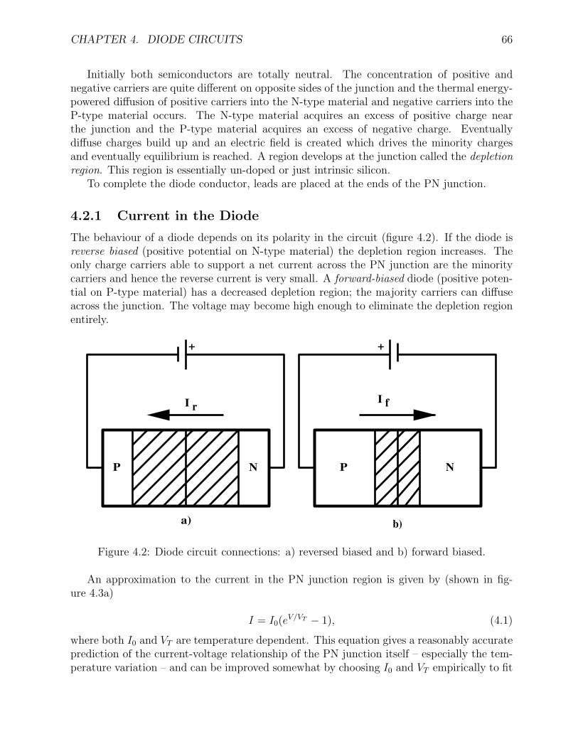
CHAPTER 4. DIODE CIRCUITS 66
Initially both semiconductors are totally neutral. The concentration of positive andnegative carriers are quite different on opposite sides of the junction and the thermal energy-powered diffusion of positive carriers into the N-type material and negative carriers into theP-type material occurs. The N-type material acquires an excess of positive charge nearthe junction and the P-type material acquires an excess of negative charge. Eventuallydiffuse charges build up and an electric field is created which drives the minority chargesand eventually equilibrium is reached. A region develops at the junction called the depletionregion. This region is essentially un-doped or just intrinsic silicon.
To complete the diode conductor, leads are placed at the ends of the PN junction.
4.2.1 Current in the Diode
The behaviour of a diode depends on its polarity in the circuit (figure 4.2). If the diode isreverse biased (positive potential on N-type material) the depletion region increases. Theonly charge carriers able to support a net current across the PN junction are the minoritycarriers and hence the reverse current is very small. A forward-biased diode (positive poten-tial on P-type material) has a decreased depletion region; the majority carriers can diffuseacross the junction. The voltage may become high enough to eliminate the depletion regionentirely.
P N
a)
+
I r
P N
b)
+
fI
Figure 4.2: Diode circuit connections: a) reversed biased and b) forward biased.
An approximation to the current in the PN junction region is given by (shown in fig-ure 4.3a)
I = I0(eV/VT − 1), (4.1)
where both I0 and VT are temperature dependent. This equation gives a reasonably accurateprediction of the current-voltage relationship of the PN junction itself – especially the tem-perature variation – and can be improved somewhat by choosing I0 and VT empirically to fit
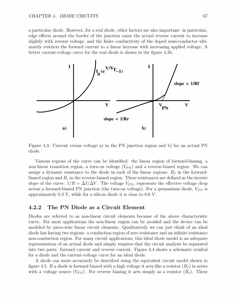
CHAPTER 4. DIODE CIRCUITS 67
a particular diode. However, for a real diode, other factors are also important: in particular,edge effects around the border of the junction cause the actual reverse current to increaseslightly with reverse voltage, and the finite conductivity of the doped semi-conductor ulti-mately restricts the forward current to a linear increase with increasing applied voltage. Abetter current-voltage curve for the real diode is shown in the figure 4.3b.
a)
I
V
I0(e
V/VT−1)
b)
I
V
slope = 1/Rr
slope = 1/Rf
VPN
Figure 4.3: Current versus voltage a) in the PN junction region and b) for an actual PNdiode.
Various regions of the curve can be identified: the linear region of forward-biasing, anon-linear transition region, a turn-on voltage (VPN) and a reverse-biased region. We canassign a dynamic resistance to the diode in each of the linear regions: Rf in the forward-biased region and Rr in the reverse-biased region. These resistances are defined as the inverseslope of the curve: 1/R = ∆I/∆V . The voltage VPN , represents the effective voltage dropacross a forward-biased PN junction (the turn-on voltage). For a germanium diode, VPN isapproximately 0.3 V, while for a silicon diode it is close to 0.6 V.
4.2.2 The PN Diode as a Circuit Element
Diodes are referred to as non-linear circuit elements because of the above characteristiccurve. For most applications the non-linear region can be avoided and the device can bemodeled by piece-wise linear circuit elements. Qualitatively we can just think of an idealdiode has having two regions: a conduction region of zero resistance and an infinite resistancenon-conduction region. For many circuit applications, this ideal diode model is an adequaterepresentation of an actual diode and simply requires that the circuit analysis be separatedinto two parts: forward current and reverse current. Figure 4.4 shows a schematic symbolfor a diode and the current-voltage curve for an ideal diode.
A diode can more accurately be described using the equivalent circuit model shown infigure 4.5. If a diode is forward biased with a high voltage it acts like a resistor (Rf ) in serieswith a voltage source (VPN). For reverse biasing it acts simply as a resistor (Rr). These
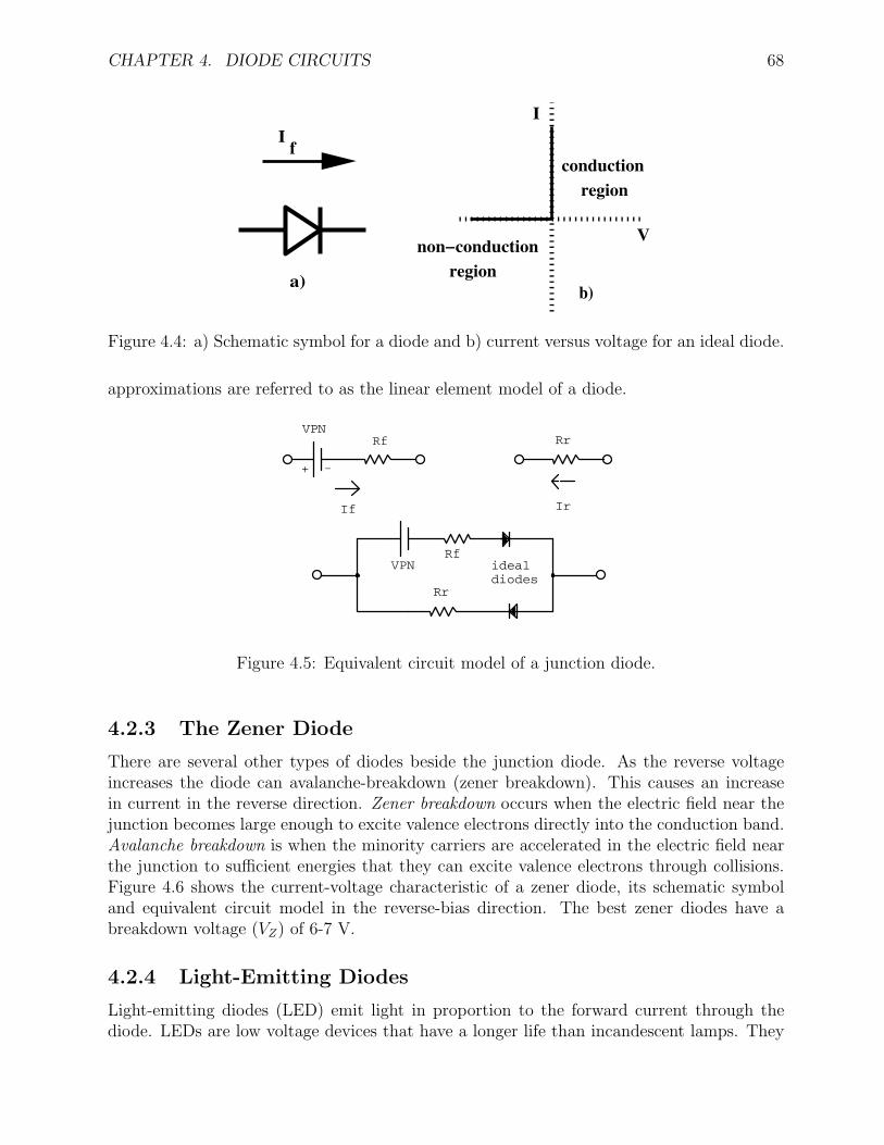
CHAPTER 4. DIODE CIRCUITS 68
b)
conductionregion
non−conductionregion
I
V
If
a)
Figure 4.4: a) Schematic symbol for a diode and b) current versus voltage for an ideal diode.
approximations are referred to as the linear element model of a diode.
idealdiodes
Ir
-+
If
VPNRrRf
Rr
RfVPN
Figure 4.5: Equivalent circuit model of a junction diode.
4.2.3 The Zener Diode
There are several other types of diodes beside the junction diode. As the reverse voltageincreases the diode can avalanche-breakdown (zener breakdown). This causes an increasein current in the reverse direction. Zener breakdown occurs when the electric field near thejunction becomes large enough to excite valence electrons directly into the conduction band.Avalanche breakdown is when the minority carriers are accelerated in the electric field nearthe junction to sufficient energies that they can excite valence electrons through collisions.Figure 4.6 shows the current-voltage characteristic of a zener diode, its schematic symboland equivalent circuit model in the reverse-bias direction. The best zener diodes have abreakdown voltage (VZ) of 6-7 V.
4.2.4 Light-Emitting Diodes
Light-emitting diodes (LED) emit light in proportion to the forward current through thediode. LEDs are low voltage devices that have a longer life than incandescent lamps. They
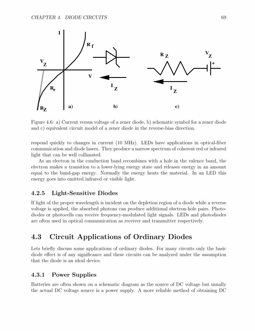
CHAPTER 4. DIODE CIRCUITS 69
I
V
a)
R f
Rr
RZ
VZ
b)
IZ
R ZV
Z+
IZ
c)
Figure 4.6: a) Current versus voltage of a zener diode, b) schematic symbol for a zener diodeand c) equivalent circuit model of a zener diode in the reverse-bias direction.
respond quickly to changes in current (10 MHz). LEDs have applications in optical-fibercommunication and diode lasers. They produce a narrow spectrum of coherent red or infraredlight that can be well collimated.
As an electron in the conduction band recombines with a hole in the valence band, theelectron makes a transition to a lower-lying energy state and releases energy in an amountequal to the band-gap energy. Normally the energy heats the material. In an LED thisenergy goes into emitted infrared or visible light.
4.2.5 Light-Sensitive Diodes
If light of the proper wavelength is incident on the depletion region of a diode while a reversevoltage is applied, the absorbed photons can produce additional electron-hole pairs. Photo-diodes or photocells can receive frequency-modulated light signals. LEDs and photodiodesare often used in optical communication as receiver and transmitter respectively.
4.3 Circuit Applications of Ordinary Diodes
Lets briefly discuss some applications of ordinary diodes. For many circuits only the basicdiode effect is of any significance and these circuits can be analyzed under the assumptionthat the diode is an ideal device.
4.3.1 Power Supplies
Batteries are often shown on a schematic diagram as the source of DC voltage but usuallythe actual DC voltage source is a power supply. A more reliable method of obtaining DC
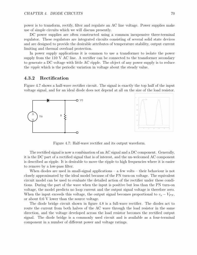
CHAPTER 4. DIODE CIRCUITS 70
power is to transform, rectify, filter and regulate an AC line voltage. Power supplies makeuse of simple circuits which we will discuss presently.
DC power supplies are often constructed using a common inexpensive three-terminalregulator. These regulators are integrated circuits consisting of several solid state devicesand are designed to provide the desirable attributes of temperature stability, output currentlimiting and thermal overload protection.
In power supply applications it is common to use a transformer to isolate the powersupply from the 110 V AC line. A rectifier can be connected to the transformer secondaryto generate a DC voltage with little AC ripple. The object of any power supply is to reducethe ripple which is the periodic variation in voltage about the steady value.
4.3.2 Rectification
Figure 4.7 shows a half-wave rectifier circuit. The signal is exactly the top half of the inputvoltage signal, and for an ideal diode does not depend at all on the size of the load resistor.
V0
Vs RS
G
Figure 4.7: Half-wave rectifier and its output waveform.
The rectified signal is now a combination of an AC signal and a DC component. Generally,it is the DC part of a rectified signal that is of interest, and the un-welcomed AC componentis described as ripple. It is desirable to move the ripple to high frequencies where it is easierto remove by a low-pass filter.
When diodes are used in small-signal applications – a few volts – their behaviour is notclosely approximated by the ideal model because of the PN turn-on voltage. The equivalentcircuit model can be used to evaluate the detailed action of the rectifier under these condi-tions. During the part of the wave when the input is positive but less than the PN turn-onvoltage, the model predicts no loop current and the output signal voltage is therefore zero.When the input exceeds this voltage, the output signal becomes proportional to vs − VPN ,or about 0.6 V lower than the source voltage.
The diode bridge circuit shown in figure 4.8 is a full-wave rectifier. The diodes act toroute the current from both halves of the AC wave through the load resistor in the samedirection, and the voltage developed across the load resistor becomes the rectified outputsignal. The diode bridge is a commonly used circuit and is available as a four-terminalcomponent in a number of different power and voltage ratings.
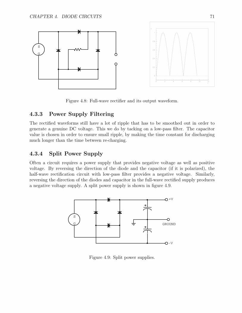
CHAPTER 4. DIODE CIRCUITS 71
S
G
Figure 4.8: Full-wave rectifier and its output waveform.
4.3.3 Power Supply Filtering
The rectified waveforms still have a lot of ripple that has to be smoothed out in order togenerate a genuine DC voltage. This we do by tacking on a low-pass filter. The capacitorvalue is chosen in order to ensure small ripple, by making the time constant for dischargingmuch longer than the time between re-charging.
4.3.4 Split Power Supply
Often a circuit requires a power supply that provides negative voltage as well as positivevoltage. By reversing the direction of the diode and the capacitor (if it is polarized), thehalf-wave rectification circuit with low-pass filter provides a negative voltage. Similarly,reversing the direction of the diodes and capacitor in the full-wave rectified supply producesa negative voltage supply. A split power supply is shown in figure 4.9.
GROUND
-V
+V
S
G
Figure 4.9: Split power supplies.
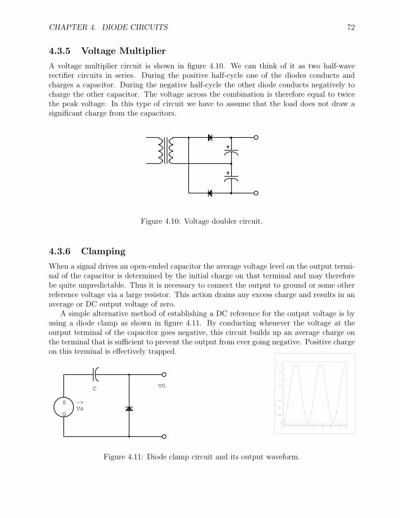
CHAPTER 4. DIODE CIRCUITS 72
4.3.5 Voltage Multiplier
A voltage multiplier circuit is shown in figure 4.10. We can think of it as two half-waverectifier circuits in series. During the positive half-cycle one of the diodes conducts andcharges a capacitor. During the negative half-cycle the other diode conducts negatively tocharge the other capacitor. The voltage across the combination is therefore equal to twicethe peak voltage. In this type of circuit we have to assume that the load does not draw asignificant charge from the capacitors.
Figure 4.10: Voltage doubler circuit.
4.3.6 Clamping
When a signal drives an open-ended capacitor the average voltage level on the output termi-nal of the capacitor is determined by the initial charge on that terminal and may thereforebe quite unpredictable. Thus it is necessary to connect the output to ground or some otherreference voltage via a large resistor. This action drains any excess charge and results in anaverage or DC output voltage of zero.
A simple alternative method of establishing a DC reference for the output voltage is byusing a diode clamp as shown in figure 4.11. By conducting whenever the voltage at theoutput terminal of the capacitor goes negative, this circuit builds up an average charge onthe terminal that is sufficient to prevent the output from ever going negative. Positive chargeon this terminal is effectively trapped.
V0C
->Vs
S
G
Figure 4.11: Diode clamp circuit and its output waveform.
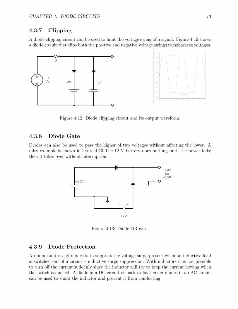
CHAPTER 4. DIODE CIRCUITS 73
4.3.7 Clipping
A diode clipping circuit can be used to limit the voltage swing of a signal. Figure 4.12 showsa diode circuit that clips both the positive and negative voltage swings to references voltages.
+
++V1 -V2
R
->Vs
S
G
Figure 4.12: Diode clipping circuit and its output waveform.
4.3.8 Diode Gate
Diodes can also be used to pass the higher of two voltages without affecting the lower. Anifty example is shown in figure 4.13 The 12 V battery does nothing until the power fails;then it takes over without interruption.
+12V to+15V
+15V
-
- +
12V
Figure 4.13: Diode OR gate.
4.3.9 Diode Protection
An important use of diodes is to suppress the voltage surge present when an inductive loadis switched out of a circuit – inductive surge suppression. With inductors it is not possibleto turn off the current suddenly since the inductor will try to keep the current flowing whenthe switch is opened. A diode in a DC circuit or back-to-back zener diodes in an AC circuitcan be used to shunt the inductor and prevent it from conducting.
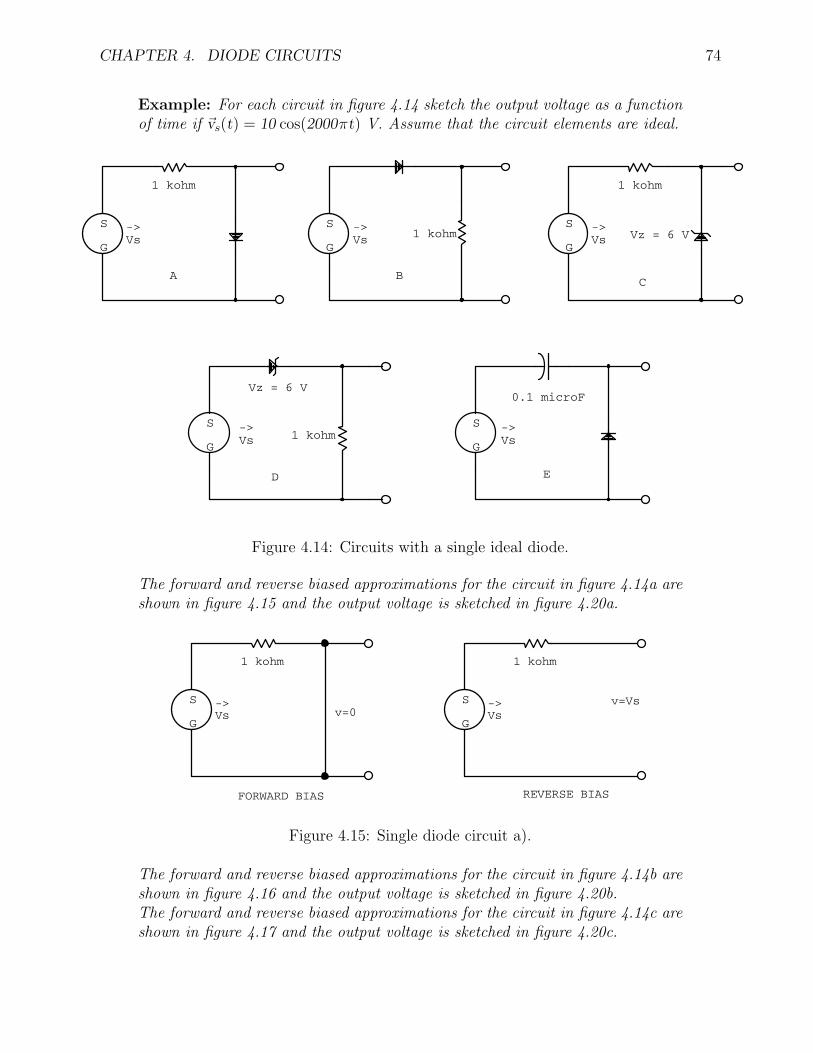
CHAPTER 4. DIODE CIRCUITS 74
Example: For each circuit in figure 4.14 sketch the output voltage as a functionof time if vs(t) = 10 cos(2000πt) V. Assume that the circuit elements are ideal.
ED
CBA
Vz = 6 V
Vz = 6 V0.1 microF
1 kohm
1 kohm
1 kohm
1 kohm
->Vs
->Vs
->Vs
->Vs
->Vs
S
G
S
G
S
G
S
G
S
G
Figure 4.14: Circuits with a single ideal diode.
The forward and reverse biased approximations for the circuit in figure 4.14a areshown in figure 4.15 and the output voltage is sketched in figure 4.20a.
v=Vs
REVERSE BIASFORWARD BIAS
v=0
1 kohm
->Vs
1 kohm
->Vs
S
G
S
G
Figure 4.15: Single diode circuit a).
The forward and reverse biased approximations for the circuit in figure 4.14b areshown in figure 4.16 and the output voltage is sketched in figure 4.20b.The forward and reverse biased approximations for the circuit in figure 4.14c areshown in figure 4.17 and the output voltage is sketched in figure 4.20c.
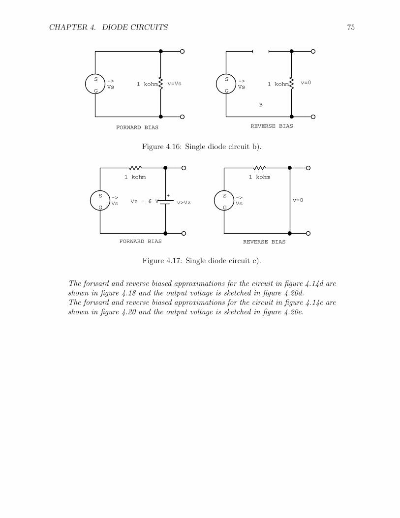
CHAPTER 4. DIODE CIRCUITS 75
v=0v=Vs
REVERSE BIASFORWARD BIAS
B
1 kohm->Vs1 kohm
->Vs
S
G
S
G
Figure 4.16: Single diode circuit b).
+v>Vz v=0
REVERSE BIASFORWARD BIAS
Vz = 6 V
1 kohm
->Vs
1 kohm
->Vs
S
G
S
G
Figure 4.17: Single diode circuit c).
The forward and reverse biased approximations for the circuit in figure 4.14d areshown in figure 4.18 and the output voltage is sketched in figure 4.20d.The forward and reverse biased approximations for the circuit in figure 4.14e areshown in figure 4.20 and the output voltage is sketched in figure 4.20e.
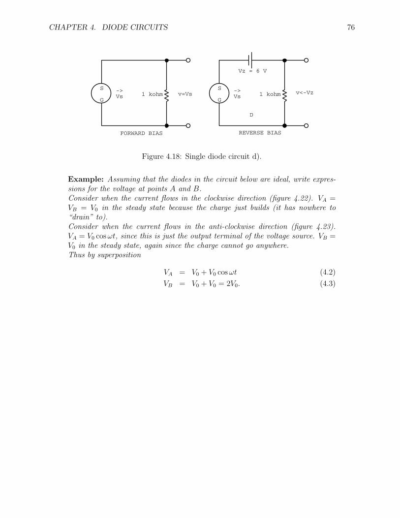
CHAPTER 4. DIODE CIRCUITS 76
v<-Vzv=Vs
REVERSE BIASFORWARD BIAS
D
Vz = 6 V
1 kohm->Vs1 kohm
->Vs
S
G
S
G
Figure 4.18: Single diode circuit d).
Example: Assuming that the diodes in the circuit below are ideal, write expres-sions for the voltage at points A and B.Consider when the current flows in the clockwise direction (figure 4.22). VA =VB = V0 in the steady state because the charge just builds (it has nowhere to“drain” to).Consider when the current flows in the anti-clockwise direction (figure 4.23).VA = V0 cos ωt, since this is just the output terminal of the voltage source. VB =V0 in the steady state, again since the charge cannot go anywhere.Thus by superposition
VA = V0 + V0 cos ωt (4.2)
VB = V0 + V0 = 2V0. (4.3)
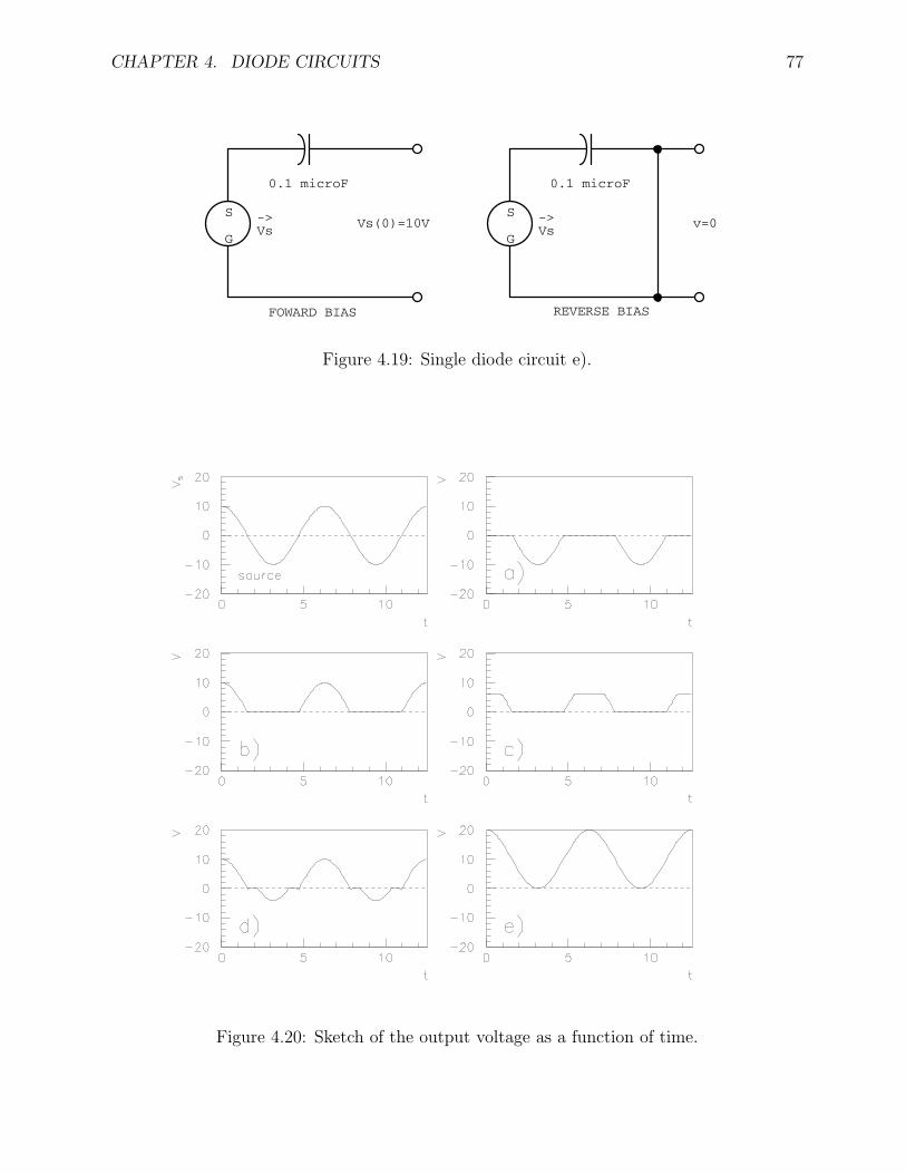
CHAPTER 4. DIODE CIRCUITS 77
Vs(0)=10V v=0
REVERSE BIASFOWARD BIAS
0.1 microF
->Vs
0.1 microF
->Vs
S
G
S
G
Figure 4.19: Single diode circuit e).
Figure 4.20: Sketch of the output voltage as a function of time.
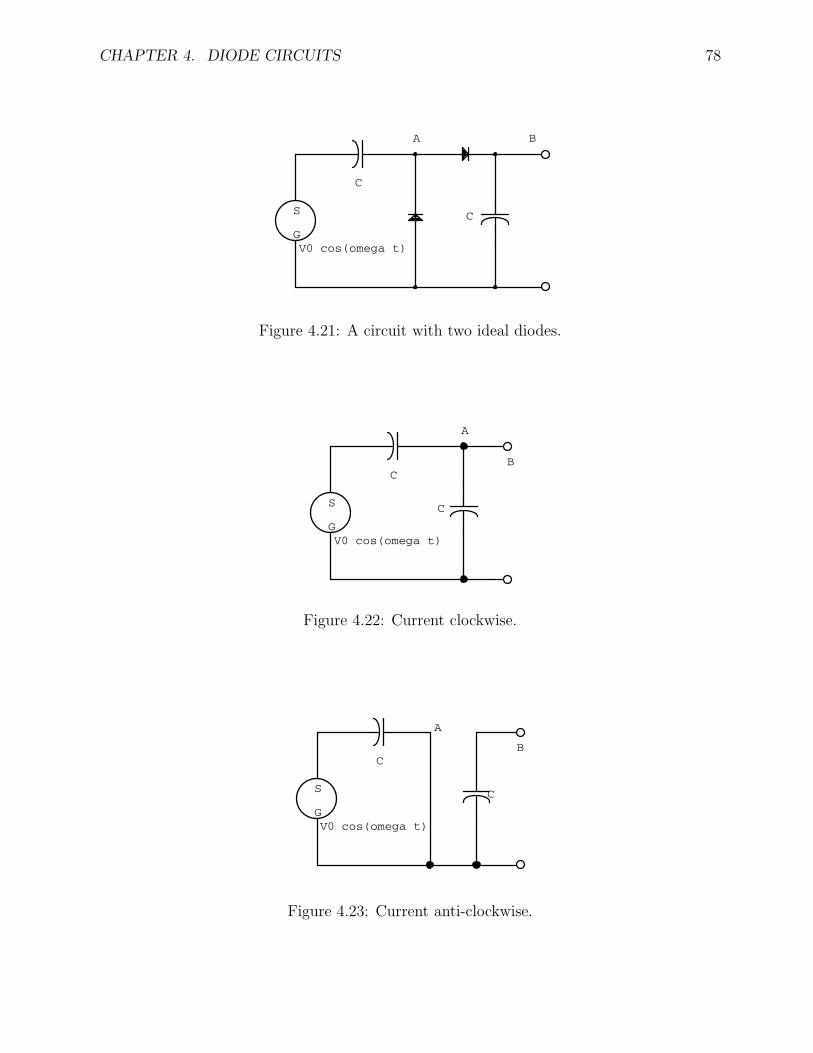
CHAPTER 4. DIODE CIRCUITS 78
V0 cos(omega t)
BA
C
C
S
G
Figure 4.21: A circuit with two ideal diodes.
V0 cos(omega t)
B
A
C
C
S
G
Figure 4.22: Current clockwise.
V0 cos(omega t)
B
A
C
C
S
G
Figure 4.23: Current anti-clockwise.
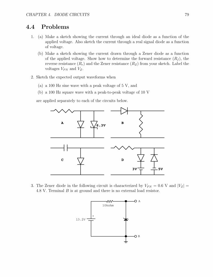
CHAPTER 4. DIODE CIRCUITS 79
4.4 Problems
1. (a) Make a sketch showing the current through an ideal diode as a function of theapplied voltage. Also sketch the current through a real signal diode as a functionof voltage.
(b) Make a sketch showing the current drawn through a Zener diode as a functionof the applied voltage. Show how to determine the forward resistance (Rf ), thereverse resistance (Rr) and the Zener resistance (RZ) from your sketch. Label thevoltages VPN and VZ .
2. Sketch the expected output waveforms when
(a) a 100 Hz sine wave with a peak voltage of 5 V, and
(b) a 100 Hz square wave with a peak-to-peak voltage of 10 V
are applied separately to each of the circuits below.
6.3V
5V3V
D
A
C
B
3. The Zener diode in the following circuit is characterized by VPN = 0.6 V and |VZ | =4.8 V. Terminal B is at ground and there is no external load resistor.
+13.2V
10kohm
B
A
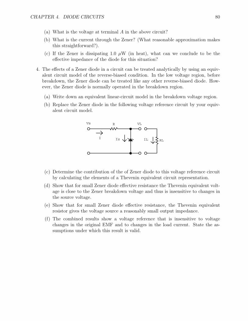
CHAPTER 4. DIODE CIRCUITS 80
(a) What is the voltage at terminal A in the above circuit?
(b) What is the current through the Zener? (What reasonable approximation makesthis straightforward?).
(c) If the Zener is dissipating 1.0 µW (in heat), what can we conclude to be theeffective impedance of the diode for this situation?
4. The effects of a Zener diode in a circuit can be treated analytically by using an equiv-alent circuit model of the reverse-biased condition. In the low voltage region, beforebreakdown, the Zener diode can be treated like any other reverse-biased diode. How-ever, the Zener diode is normally operated in the breakdown region.
(a) Write down an equivalent linear-circuit model in the breakdown voltage region.
(b) Replace the Zener diode in the following voltage reference circuit by your equiv-alent circuit model.
VL
RLILIz
Vs
I
R
(c) Determine the contribution of the of Zener diode to this voltage reference circuitby calculating the elements of a Thevenin equivalent circuit representation.
(d) Show that for small Zener diode effective resistance the Thevenin equivalent volt-age is close to the Zener breakdown voltage and thus is insensitive to changes inthe source voltage.
(e) Show that for small Zener diode effective resistance, the Thevenin equivalentresistor gives the voltage source a reasonably small output impedance.
(f) The combined results show a voltage reference that is insensitive to voltagechanges in the original EMF and to changes in the load current. State the as-sumptions under which this result is valid.
Chapter 5
Transistor Circuits
The circuits we have encountered so far are passive and dissipate power. Even a transformerthat is capable of giving a voltage gain to a circuit is not an active element. Active elementsin a circuit increase the power by controlling or modulating the flow of energy or power froman additional power supply into the circuit.
Transistors are active circuit elements and are typically made from silicon or germaniumand come in two types. The bipolar transistor controls the current by varying the numberof charge carriers. The field effect transistor (FET) varies the current by varying the shapeof the conducting volume.
Before starting we will define some notation. The voltages that are with respect toground are indicated by a single subscript. Voltages with repeated letters are power supplyvoltages. And voltages between two terminals are indicated by a double subscript.
5.1 Bipolar Junction Transistors
By placing two PN junctions together we can create a bipolar transistor. In a PNP transistorthe majority charge carriers are holes and germanium is favoured for these devices. Siliconis best for NPN transistors where the majority charge carriers are electrons.
The thin and lightly doped central region is known as the base (B) and has majoritycharge carriers of opposite polarity to those in the surrounding material. The two outerregions are known as the emitter (E) and the collector (C). Under the proper operatingconditions the emitter will emit or inject majority charge carriers into the base region, andbecause the base is very thin, most will ultimately reach the collector. The emitter is highlydoped to reduce resistance. The collector is lightly doped to reduce the junction capacitanceof the collector-base junction.
The schematic circuit symbols for bipolar transistors are shown in figure 5.1. The arrowson the schematic symbols indicate the direction of both IB and IC . The collector is usuallyat a higher voltage than the emitter. The emitter-base junction is forward biased while thecollector-base junction is reversed biased.
81
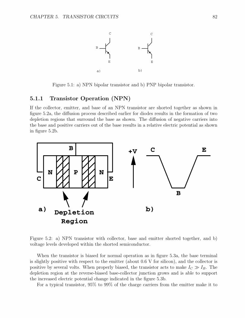
CHAPTER 5. TRANSISTOR CIRCUITS 82
b)a)
EE
CC
BB
Figure 5.1: a) NPN bipolar transistor and b) PNP bipolar transistor.
5.1.1 Transistor Operation (NPN)
If the collector, emitter, and base of an NPN transistor are shorted together as shown infigure 5.2a, the diffusion process described earlier for diodes results in the formation of twodepletion regions that surround the base as shown. The diffusion of negative carriers intothe base and positive carriers out of the base results in a relative electric potential as shownin figure 5.2b.
N P NC
B
E
a) DepletionRegion
+V C E
B
b)
Figure 5.2: a) NPN transistor with collector, base and emitter shorted together, and b)voltage levels developed within the shorted semiconductor.
When the transistor is biased for normal operation as in figure 5.3a, the base terminalis slightly positive with respect to the emitter (about 0.6 V for silicon), and the collector ispositive by several volts. When properly biased, the transistor acts to make IC IB. Thedepletion region at the reverse-biased base-collector junction grows and is able to supportthe increased electric potential change indicated in the figure 5.3b.
For a typical transistor, 95% to 99% of the charge carriers from the emitter make it to
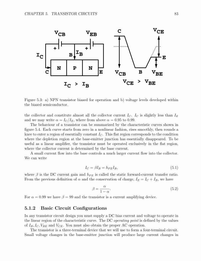
CHAPTER 5. TRANSISTOR CIRCUITS 83
N P N
VCB VEB
ICIB
IC > IB
C E
B++
C
B
E
VCE > VBE
VCB
VCE
VBE
Figure 5.3: a) NPN transistor biased for operation and b) voltage levels developed withinthe biased semiconductor.
the collector and constitute almost all the collector current IC . IC is slightly less than IE
and we may write α = IC/IE, where from above α = 0.95 to 0.99.The behaviour of a transistor can be summarized by the characteristic curves shown in
figure 5.4. Each curve starts from zero in a nonlinear fashion, rises smoothly, then rounds aknee to enter a region of essentially constant IC . This flat region corresponds to the conditionwhere the depletion region at the base-emitter junction has essentially disappeared. To beuseful as a linear amplifier, the transistor must be operated exclusively in the flat region,where the collector current is determined by the base current.
A small current flow into the base controls a much larger current flow into the collector.We can write
IC = βIB = hFEIB, (5.1)
where β is the DC current gain and hFE is called the static forward-current transfer ratio.From the previous definition of α and the conservation of charge, IE = IC + IB, we have
β =α
1 − α. (5.2)
For α = 0.99 we have β = 99 and the transistor is a current amplifying device.
5.1.2 Basic Circuit Configurations
In any transistor circuit design you must supply a DC bias current and voltage to operate inthe linear region of the characteristic curve. The DC operating point is defined by the valuesof IB, IC , VBE and VCE. You must also obtain the proper AC operation.
The transistor is a three-terminal device that we will use to form a four-terminal circuit.Small voltage changes in the base-emitter junction will produce large current changes in
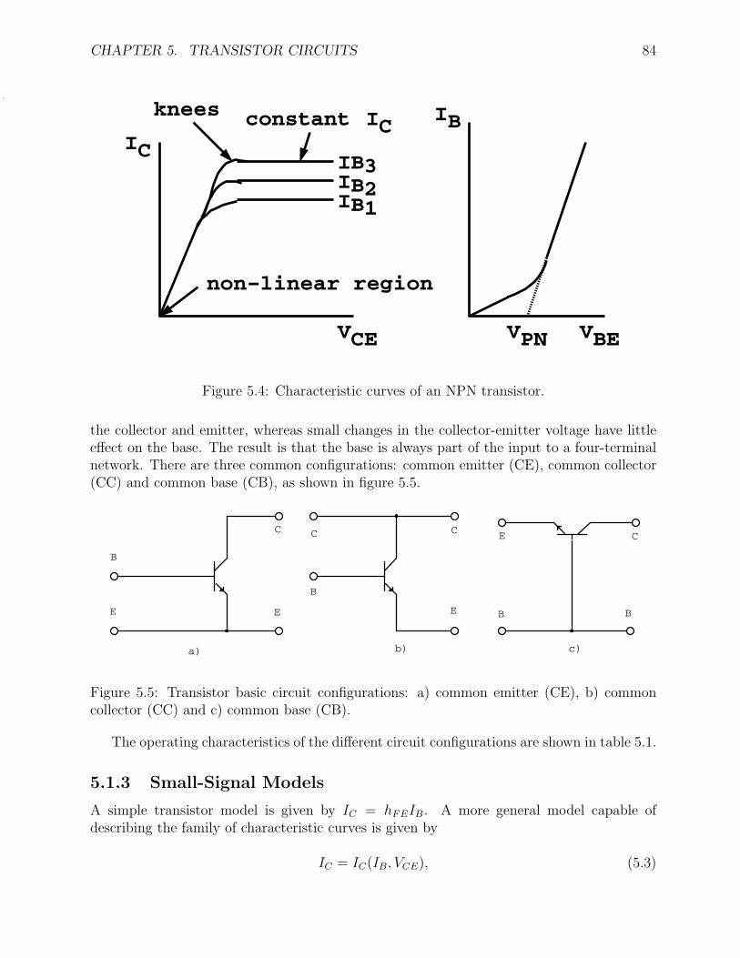
CHAPTER 5. TRANSISTOR CIRCUITS 84
IC
VCE
IB1IB2IB3
constant IC
non−linear region
knees IB
VBEVPN
Figure 5.4: Characteristic curves of an NPN transistor.
the collector and emitter, whereas small changes in the collector-emitter voltage have littleeffect on the base. The result is that the base is always part of the input to a four-terminalnetwork. There are three common configurations: common emitter (CE), common collector(CC) and common base (CB), as shown in figure 5.5.
E
c)b)a)
BB
CC
EE
B
E
CC
B
Figure 5.5: Transistor basic circuit configurations: a) common emitter (CE), b) commoncollector (CC) and c) common base (CB).
The operating characteristics of the different circuit configurations are shown in table 5.1.
5.1.3 Small-Signal Models
A simple transistor model is given by IC = hFEIB. A more general model capable ofdescribing the family of characteristic curves is given by
IC = IC(IB, VCE), (5.3)
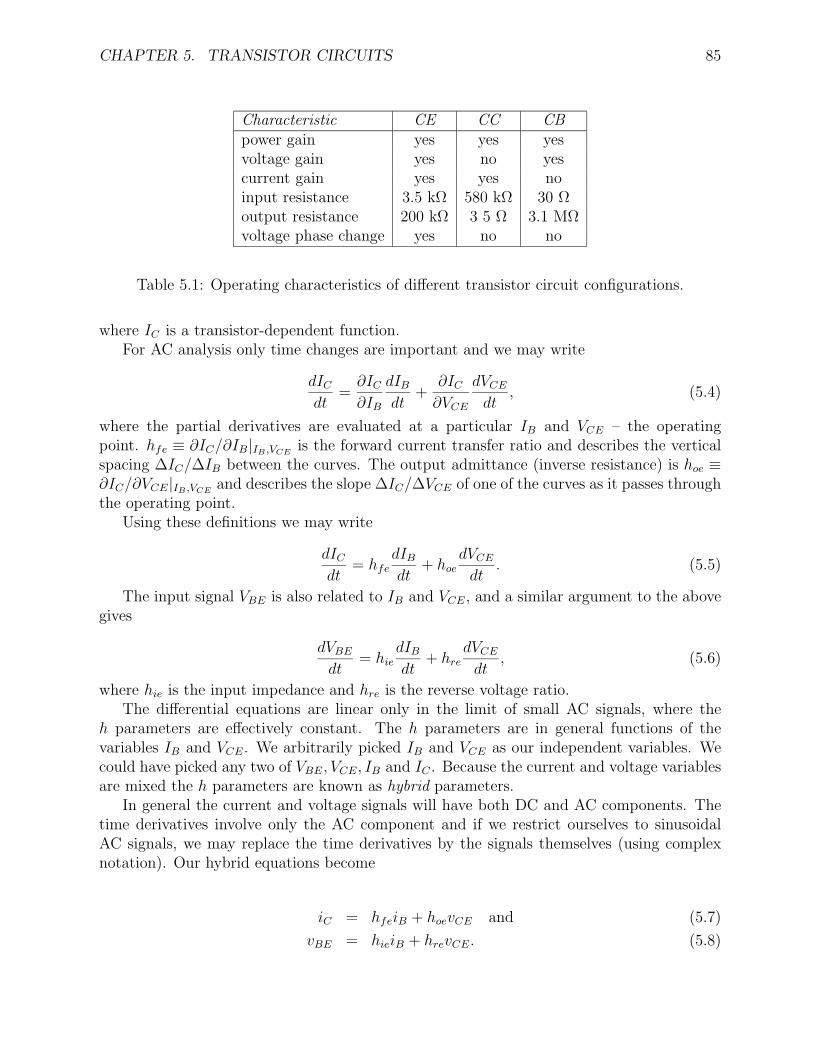
CHAPTER 5. TRANSISTOR CIRCUITS 85
Characteristic CE CC CBpower gain yes yes yesvoltage gain yes no yescurrent gain yes yes noinput resistance 3.5 kΩ 580 kΩ 30 Ωoutput resistance 200 kΩ 3 5 Ω 3.1 MΩvoltage phase change yes no no
Table 5.1: Operating characteristics of different transistor circuit configurations.
where IC is a transistor-dependent function.For AC analysis only time changes are important and we may write
dIC
dt=
∂IC
∂IB
dIB
dt+
∂IC
∂VCE
dVCE
dt, (5.4)
where the partial derivatives are evaluated at a particular IB and VCE – the operatingpoint. hfe ≡ ∂IC/∂IB|IB ,VCE
is the forward current transfer ratio and describes the verticalspacing ∆IC/∆IB between the curves. The output admittance (inverse resistance) is hoe ≡∂IC/∂VCE|IB ,VCE
and describes the slope ∆IC/∆VCE of one of the curves as it passes throughthe operating point.
Using these definitions we may write
dIC
dt= hfe
dIB
dt+ hoe
dVCE
dt. (5.5)
The input signal VBE is also related to IB and VCE, and a similar argument to the abovegives
dVBE
dt= hie
dIB
dt+ hre
dVCE
dt, (5.6)
where hie is the input impedance and hre is the reverse voltage ratio.The differential equations are linear only in the limit of small AC signals, where the
h parameters are effectively constant. The h parameters are in general functions of thevariables IB and VCE. We arbitrarily picked IB and VCE as our independent variables. Wecould have picked any two of VBE, VCE, IB and IC . Because the current and voltage variablesare mixed the h parameters are known as hybrid parameters.
In general the current and voltage signals will have both DC and AC components. Thetime derivatives involve only the AC component and if we restrict ourselves to sinusoidalAC signals, we may replace the time derivatives by the signals themselves (using complexnotation). Our hybrid equations become
iC = hfeiB + hoevCE and (5.7)
vBE = hieiB + hrevCE. (5.8)
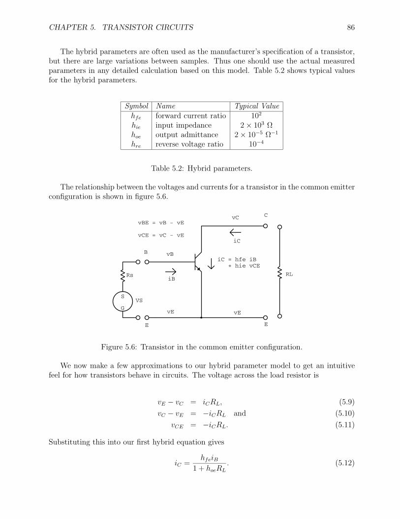
CHAPTER 5. TRANSISTOR CIRCUITS 86
The hybrid parameters are often used as the manufacturer’s specification of a transistor,but there are large variations between samples. Thus one should use the actual measuredparameters in any detailed calculation based on this model. Table 5.2 shows typical valuesfor the hybrid parameters.
Symbol Name Typical Valuehfe forward current ratio 102
hie input impedance 2 × 10³ Ωhoe output admittance 2 × 10⁻⁵ Ω−1
hre reverse voltage ratio 10−4
Table 5.2: Hybrid parameters.
The relationship between the voltages and currents for a transistor in the common emitterconfiguration is shown in figure 5.6.
iC = hfe iB + hie vCE
vBE = vB - vE
vCE = vC - vE
vB
vE vE
iB
iC
vC
RL
C
B
EE
Rs
VSS
G
Figure 5.6: Transistor in the common emitter configuration.
We now make a few approximations to our hybrid parameter model to get an intuitivefeel for how transistors behave in circuits. The voltage across the load resistor is
vE − vC = iCRL, (5.9)
vC − vE = −iCRL and (5.10)
vCE = −iCRL. (5.11)
Substituting this into our first hybrid equation gives
iC =hfeiB
1 + hoeRL
. (5.12)
CHAPTER 5. TRANSISTOR CIRCUITS 87
If hoeRL 1 (good to about 10%) we can write
iC = hfeiB, (5.13)
which is the AC equivalent of IC = βIB = hFEIB. Similarly, using the second hybridequation gives
vCE
vBE
= − RLhfe
hie − RLhfehie
. (5.14)
If RLhfehre 1 (good to about 10%) we have
vCE
vBE
= −hfe
hie
RL, (5.15)
which is the AC voltage gain.
5.1.4 Ideal and Perfect Bipolar Transistor Models
By ignoring hoe and hre we can define a simplified AC model for the transistor (perfecttransistor) that is independent of the circuit configuration:
iC = hfeiB and (5.16)
vBE = hieiB. (5.17)
There is no PN voltage drop in these equations since it is a DC effect.Since iC is typically 100 times larger than iB we can make the approximation iE ≈ iC .
An ideal transistor is defined such that hie = 0 and hence vB = vE. When the effects of hie
cannot be ignored, we can use the perfect transistor model as described by the two equationsabove. On a circuit diagram hie can be added directly to the ideal transistor symbol.
The ideal transistor model has the following two working rules:
1. The base and emitter are at the same AC voltage (vB = vE). They differ only by aconstant DC potential VPN .
2. The collector current is equal to the emitter current and proportional to the basecurrent (iE = iC , IE = IC , iC = hfeiB and IC = hFEiB).
5.1.5 Transconductance Model
The transconductance model provides an alternative description of transistor operation. Theforward transconductance, which has units of inverse resistance, is defined as gm = hfe/hie.Using the perfect transistor model we can write
iC = gm(vB − vE) = gmvBE. (5.18)
Since the transconductance is used to describe field effect transistors, it is sometimes conve-nient to apply the same parameter to bipolar transistors.
CHAPTER 5. TRANSISTOR CIRCUITS 88
We now turn to the description of some simple amplifiers that use a single bipolar tran-sistor. Our goal will be to estimate the voltage gains, current gains, input impedances,output impedances and corner frequencies of the amplifiers. The characteristics of a perfectamplifier are as follows:
• infinite input impedance (the amplifier draws no current),
• zero output impedance,
• infinite voltage and current gain, and
• stable, linear, etc.
5.2 The Common Emitter Amplifier
The common emitter configuration is the most versatile of the three. It has low inputimpedance, moderate output impedance, voltage gain and current gain. The input andoutput are often capacitively coupled. Before performing an AC analysis we will discuss DCbiasing.
5.2.1 DC Biasing
DC biasing is setting up a circuit to operate a transistor at a desired operating point on itscharacteristic curve. Three bias networks for the common emitter amplifier are shown infigure 5.7.
In figure 5.7a the only path for DC bias current into the base is through RB. VCC is apower supply voltage which is generally greater than 10 V such that VPN can be ignored. TheDC voltage at the collector should be large enough to provide at least a 2 V drop betweencollector and emitter and clearly must be less than VCC . In the absence of other circuitrequirements, a convenient algebraic choice for VC is VCC/2. DC circuit analysis results inthe following relative sizes of the two resistors:
RB = 2hFERC . (5.19)
Although the circuit works reasonably well, the fact that hFE is quite variable amongsamples leads to a bad design. A well-designed circuit should have an operating point thatis less dependent on this parameter.
Figure 5.7b shows a network with the base-biasing resistor connected to the collectorinstead of VCC . RF acts as a negative feedback resistor since it feeds the collector currentback into the base. Analysis gives
RF = hFERC . (5.20)
Therefore a change in hFE has only half the effect of the previous design.A more common bias stabilization technique employs a series resistor between the emitter
and ground. This circuit has about the same sensitivity to changes in hFE as the previouscircuit.
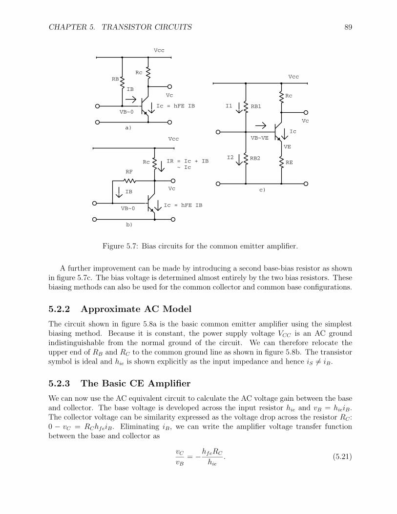
CHAPTER 5. TRANSISTOR CIRCUITS 89
c)
b)
a)Ic
Rc
VE
RE
Vc
Vcc
VB~VE
RB2
RB1
I2
I1
IR = Ic + IB ~ Ic
Ic = hFE IB
VcIB
VB~0
RcRB
Vcc
Ic = hFE IB
Vc
VB~0
Vcc
IB
Rc
RF
Figure 5.7: Bias circuits for the common emitter amplifier.
A further improvement can be made by introducing a second base-bias resistor as shownin figure 5.7c. The bias voltage is determined almost entirely by the two bias resistors. Thesebiasing methods can also be used for the common collector and common base configurations.
5.2.2 Approximate AC Model
The circuit shown in figure 5.8a is the basic common emitter amplifier using the simplestbiasing method. Because it is constant, the power supply voltage VCC is an AC groundindistinguishable from the normal ground of the circuit. We can therefore relocate theupper end of RB and RC to the common ground line as shown in figure 5.8b. The transistorsymbol is ideal and hie is shown explicitly as the input impedance and hence iS = iB.
5.2.3 The Basic CE Amplifier
We can now use the AC equivalent circuit to calculate the AC voltage gain between the baseand collector. The base voltage is developed across the input resistor hie and vB = hieiB.The collector voltage can be similarity expressed as the voltage drop across the resistor RC :0 − vC = RChfeiB. Eliminating iB, we can write the amplifier voltage transfer functionbetween the base and collector as
vC
vB
= −hfeRC
hie
. (5.21)
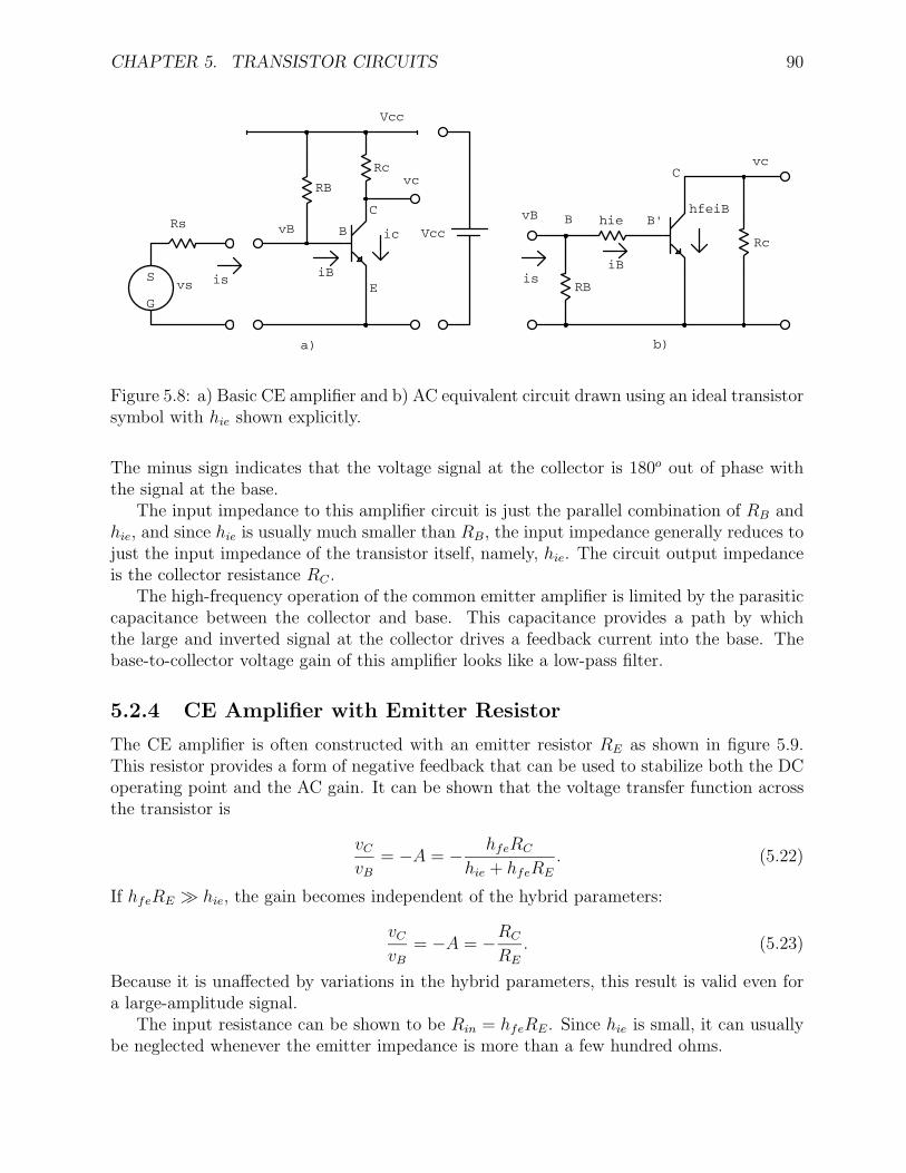
CHAPTER 5. TRANSISTOR CIRCUITS 90
b)
hfeiBhie
iB
RBis
vB B'B
Rc
vcC
a)
isvs
Rs vB
iB
B
RB
Rc
C
E
ic
vc
Vcc
Vcc
S
G
Figure 5.8: a) Basic CE amplifier and b) AC equivalent circuit drawn using an ideal transistorsymbol with hie shown explicitly.
The minus sign indicates that the voltage signal at the collector is 180o out of phase withthe signal at the base.
The input impedance to this amplifier circuit is just the parallel combination of RB andhie, and since hie is usually much smaller than RB, the input impedance generally reduces tojust the input impedance of the transistor itself, namely, hie. The circuit output impedanceis the collector resistance RC .
The high-frequency operation of the common emitter amplifier is limited by the parasiticcapacitance between the collector and base. This capacitance provides a path by whichthe large and inverted signal at the collector drives a feedback current into the base. Thebase-to-collector voltage gain of this amplifier looks like a low-pass filter.
5.2.4 CE Amplifier with Emitter Resistor
The CE amplifier is often constructed with an emitter resistor RE as shown in figure 5.9.This resistor provides a form of negative feedback that can be used to stabilize both the DCoperating point and the AC gain. It can be shown that the voltage transfer function acrossthe transistor is
vC
vB
= −A = − hfeRC
hie + hfeRE
. (5.22)
If hfeRE hie, the gain becomes independent of the hybrid parameters:
vC
vB
= −A = −RC
RE
. (5.23)
Because it is unaffected by variations in the hybrid parameters, this result is valid even fora large-amplitude signal.
The input resistance can be shown to be Rin = hfeRE. Since hie is small, it can usuallybe neglected whenever the emitter impedance is more than a few hundred ohms.
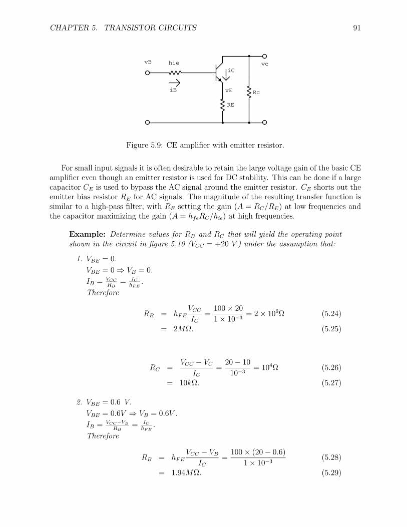
CHAPTER 5. TRANSISTOR CIRCUITS 91
vc
vE Rc
RE
iC
iB
hievB
Figure 5.9: CE amplifier with emitter resistor.
For small input signals it is often desirable to retain the large voltage gain of the basic CEamplifier even though an emitter resistor is used for DC stability. This can be done if a largecapacitor CE is used to bypass the AC signal around the emitter resistor. CE shorts out theemitter bias resistor RE for AC signals. The magnitude of the resulting transfer function issimilar to a high-pass filter, with RE setting the gain (A = RC/RE) at low frequencies andthe capacitor maximizing the gain (A = hfeRC/hie) at high frequencies.
Example: Determine values for RB and RC that will yield the operating pointshown in the circuit in figure 5.10 (VCC = +20 V ) under the assumption that:
1. VBE = 0.
VBE = 0 ⇒ VB = 0.
IB = VCC
RB= IC
hFE.
Therefore
RB = hFEVCC
IC
=100 × 20
1 × 10−3= 2 × 10⁶Ω (5.24)
= 2MΩ. (5.25)
RC =VCC − VC
IC
=20 − 10
10−3= 104Ω (5.26)
= 10kΩ. (5.27)
2. VBE = 0.6 V.
VBE = 0.6V ⇒ VB = 0.6V .
IB = VCC−VB
RB= IC
hFE.
Therefore
RB = hFEVCC − VB
IC
=100 × (20 − 0.6)
1 × 10⁻³(5.28)
= 1.94MΩ. (5.29)
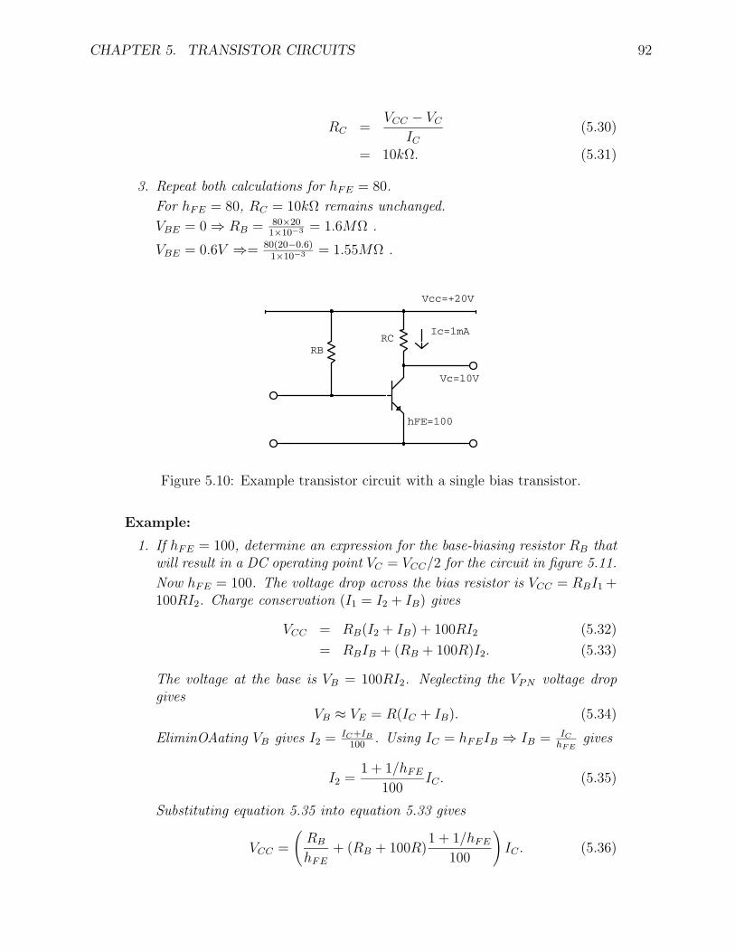
CHAPTER 5. TRANSISTOR CIRCUITS 92
RC =VCC − VC
IC
(5.30)
= 10kΩ. (5.31)
3. Repeat both calculations for hFE = 80.
For hFE = 80, RC = 10kΩ remains unchanged.
VBE = 0 ⇒ RB = 80×201×10−3 = 1.6MΩ .
VBE = 0.6V ⇒= 80(20−0.6)1×10−3 = 1.55MΩ .
Ic=1mA
hFE=100
Vc=10V
Vcc=+20V
RCRB
Figure 5.10: Example transistor circuit with a single bias transistor.
Example:
1. If hFE = 100, determine an expression for the base-biasing resistor RB thatwill result in a DC operating point VC = VCC/2 for the circuit in figure 5.11.
Now hFE = 100. The voltage drop across the bias resistor is VCC = RBI1 +100RI2. Charge conservation (I1 = I2 + IB) gives
VCC = RB(I2 + IB) + 100RI2 (5.32)
= RBIB + (RB + 100R)I2. (5.33)
The voltage at the base is VB = 100RI2. Neglecting the VPN voltage dropgives
VB ≈ VE = R(IC + IB). (5.34)
EliminOAating VB gives I2 = IC+IB
100. Using IC = hFEIB ⇒ IB = IC
hFEgives
I2 =1 + 1/hFE
100IC . (5.35)
Substituting equation 5.35 into equation 5.33 gives
VCC =
(RB
hFE
+ (RB + 100R)1 + 1/hFE
100
)IC . (5.36)
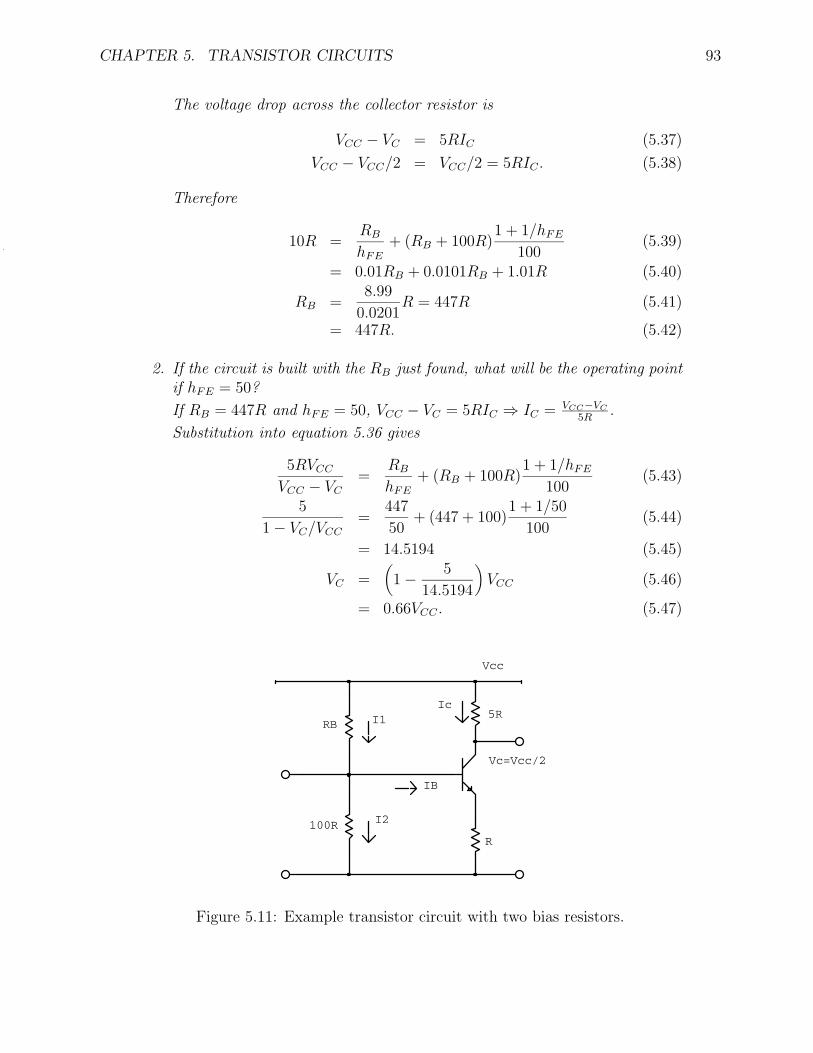
CHAPTER 5. TRANSISTOR CIRCUITS 93
The voltage drop across the collector resistor is
VCC − VC = 5RIC (5.37)
VCC − VCC/2 = VCC/2 = 5RIC . (5.38)
Therefore
10R =RB
hFE
+ (RB + 100R)1 + 1/hFE
100(5.39)
= 0.01RB + 0.0101RB + 1.01R (5.40)
RB =8.99
0.0201R = 447R (5.41)
= 447R. (5.42)
2. If the circuit is built with the RB just found, what will be the operating pointif hFE = 50?
If RB = 447R and hFE = 50, VCC − VC = 5RIC ⇒ IC = VCC−VC
5R.
Substitution into equation 5.36 gives
5RVCC
VCC − VC
=RB
hFE
+ (RB + 100R)1 + 1/hFE
100(5.43)
5
1 − VC/VCC
=447
50+ (447 + 100)
1 + 1/50
100(5.44)
= 14.5194 (5.45)
VC =(1 − 5
14.5194
)VCC (5.46)
= 0.66VCC . (5.47)
Ic
Vc=Vcc/2
Vcc
5R
R
IB
I2
I1
100R
RB
Figure 5.11: Example transistor circuit with two bias resistors.
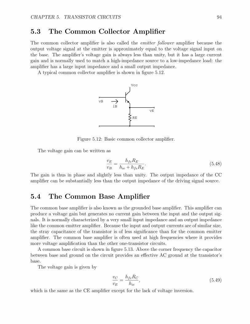
CHAPTER 5. TRANSISTOR CIRCUITS 94
5.3 The Common Collector Amplifier
The common collector amplifier is also called the emitter follower amplifier because theoutput voltage signal at the emitter is approximately equal to the voltage signal input onthe base. The amplifier’s voltage gain is always less than unity, but it has a large currentgain and is normally used to match a high-impedance source to a low-impedance load: theamplifier has a large input impedance and a small output impedance.
A typical common collector amplifier is shown in figure 5.12.
RE
vE
Vcc
iB
vB
Figure 5.12: Basic common collector amplifier.
The voltage gain can be written as
vE
vB
=hfeRE
hie + hfeRE
. (5.48)
The gain is thus in phase and slightly less than unity. The output impedance of the CCamplifier can be substantially less than the output impedance of the driving signal source.
5.4 The Common Base Amplifier
The common base amplifier is also known as the grounded base amplifier. This amplifier canproduce a voltage gain but generates no current gain between the input and the output sig-nals. It is normally characterized by a very small input impedance and an output impedancelike the common emitter amplifier. Because the input and output currents are of similar size,the stray capacitance of the transistor is of less significance than for the common emitteramplifier. The common base amplifier is often used at high frequencies where it providesmore voltage amplification than the other one-transistor circuits.
A common base circuit is shown in figure 5.13. Above the corner frequency the capacitorbetween base and ground on the circuit provides an effective AC ground at the transistor’sbase.
The voltage gain is given by
vC
vE
=hfeRC
hie
, (5.49)
which is the same as the CE amplifier except for the lack of voltage inversion.
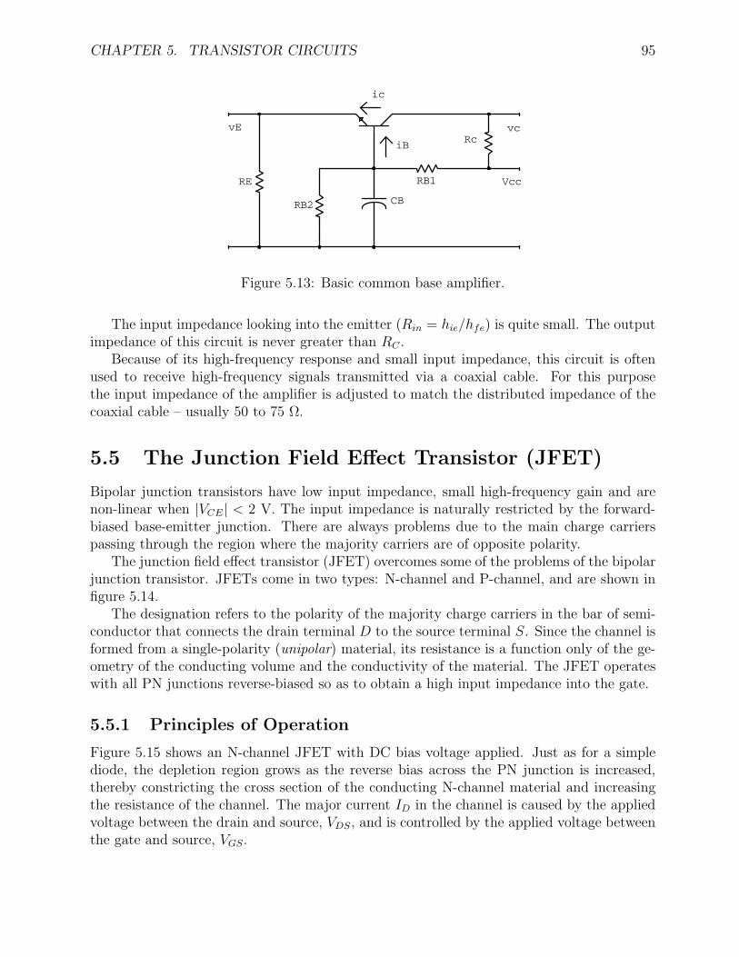
CHAPTER 5. TRANSISTOR CIRCUITS 95
Rc
ic
iB
RE
vE
RB1
RB2 CB
Vcc
vc
Figure 5.13: Basic common base amplifier.
The input impedance looking into the emitter (Rin = hie/hfe) is quite small. The outputimpedance of this circuit is never greater than RC .
Because of its high-frequency response and small input impedance, this circuit is oftenused to receive high-frequency signals transmitted via a coaxial cable. For this purposethe input impedance of the amplifier is adjusted to match the distributed impedance of thecoaxial cable – usually 50 to 75 Ω.
5.5 The Junction Field Effect Transistor (JFET)
Bipolar junction transistors have low input impedance, small high-frequency gain and arenon-linear when |VCE| < 2 V. The input impedance is naturally restricted by the forward-biased base-emitter junction. There are always problems due to the main charge carrierspassing through the region where the majority carriers are of opposite polarity.
The junction field effect transistor (JFET) overcomes some of the problems of the bipolarjunction transistor. JFETs come in two types: N-channel and P-channel, and are shown infigure 5.14.
The designation refers to the polarity of the majority charge carriers in the bar of semi-conductor that connects the drain terminal D to the source terminal S. Since the channel isformed from a single-polarity (unipolar) material, its resistance is a function only of the ge-ometry of the conducting volume and the conductivity of the material. The JFET operateswith all PN junctions reverse-biased so as to obtain a high input impedance into the gate.
5.5.1 Principles of Operation
Figure 5.15 shows an N-channel JFET with DC bias voltage applied. Just as for a simplediode, the depletion region grows as the reverse bias across the PN junction is increased,thereby constricting the cross section of the conducting N-channel material and increasingthe resistance of the channel. The major current ID in the channel is caused by the appliedvoltage between the drain and source, VDS, and is controlled by the applied voltage betweenthe gate and source, VGS.
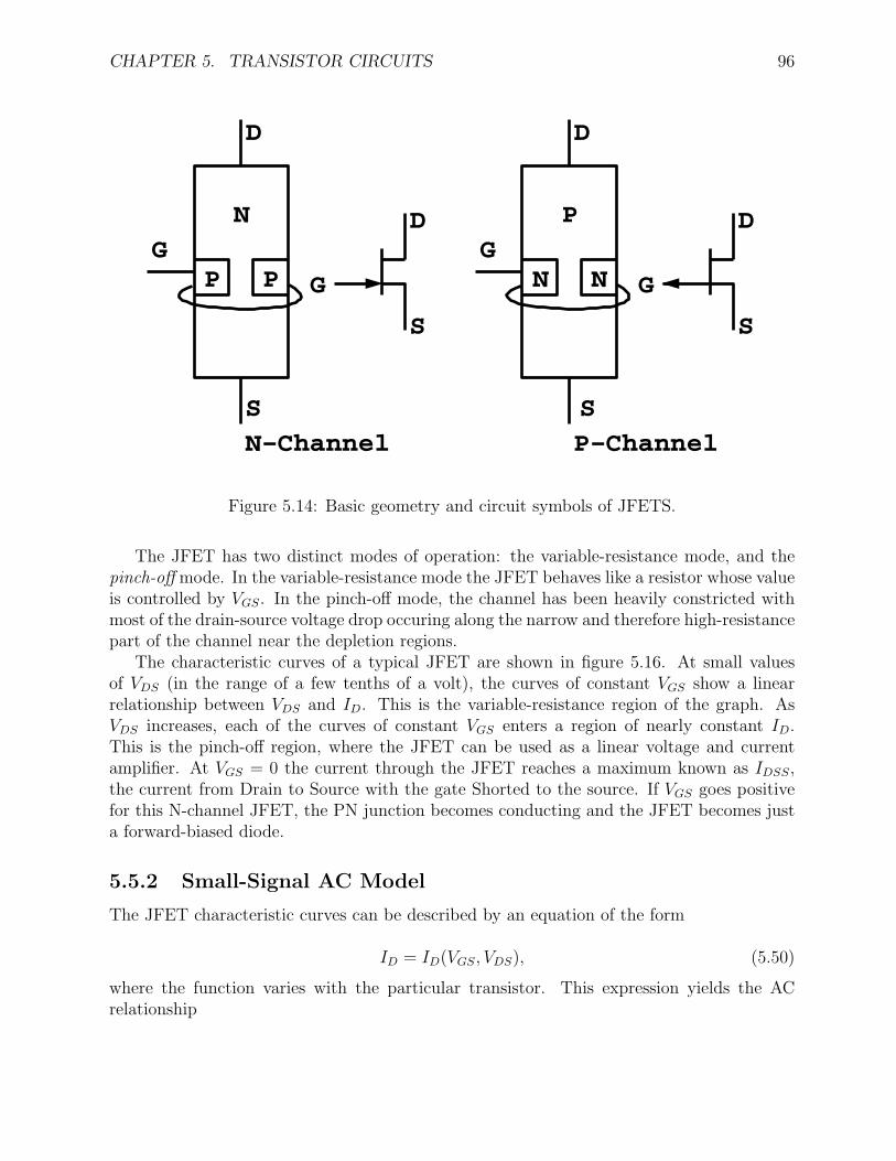
CHAPTER 5. TRANSISTOR CIRCUITS 96
D
S
GP P
N D
G
S
D
G
S
D
S
G
P
N N
N−Channel P−Channel
Figure 5.14: Basic geometry and circuit symbols of JFETS.
The JFET has two distinct modes of operation: the variable-resistance mode, and thepinch-off mode. In the variable-resistance mode the JFET behaves like a resistor whose valueis controlled by VGS. In the pinch-off mode, the channel has been heavily constricted withmost of the drain-source voltage drop occuring along the narrow and therefore high-resistancepart of the channel near the depletion regions.
The characteristic curves of a typical JFET are shown in figure 5.16. At small valuesof VDS (in the range of a few tenths of a volt), the curves of constant VGS show a linearrelationship between VDS and ID. This is the variable-resistance region of the graph. AsVDS increases, each of the curves of constant VGS enters a region of nearly constant ID.This is the pinch-off region, where the JFET can be used as a linear voltage and currentamplifier. At VGS = 0 the current through the JFET reaches a maximum known as IDSS,the current from Drain to Source with the gate Shorted to the source. If VGS goes positivefor this N-channel JFET, the PN junction becomes conducting and the JFET becomes justa forward-biased diode.
5.5.2 Small-Signal AC Model
The JFET characteristic curves can be described by an equation of the form
ID = ID(VGS, VDS), (5.50)
where the function varies with the particular transistor. This expression yields the ACrelationship
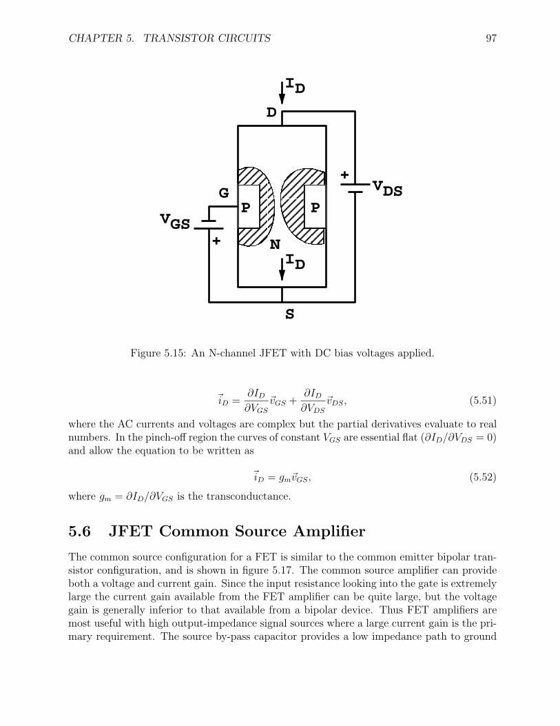
CHAPTER 5. TRANSISTOR CIRCUITS 97
D
N
PPG
S
VDS
VGS
ID
ID
+
+
Figure 5.15: An N-channel JFET with DC bias voltages applied.
iD =∂ID
∂VGS
vGS +∂ID
∂VDS
vDS, (5.51)
where the AC currents and voltages are complex but the partial derivatives evaluate to realnumbers. In the pinch-off region the curves of constant VGS are essential flat (∂ID/∂VDS = 0)and allow the equation to be written as
iD = gmvGS, (5.52)
where gm = ∂ID/∂VGS is the transconductance.
5.6 JFET Common Source Amplifier
The common source configuration for a FET is similar to the common emitter bipolar tran-sistor configuration, and is shown in figure 5.17. The common source amplifier can provideboth a voltage and current gain. Since the input resistance looking into the gate is extremelylarge the current gain available from the FET amplifier can be quite large, but the voltagegain is generally inferior to that available from a bipolar device. Thus FET amplifiers aremost useful with high output-impedance signal sources where a large current gain is the pri-mary requirement. The source by-pass capacitor provides a low impedance path to ground
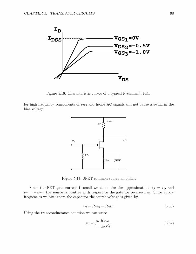
CHAPTER 5. TRANSISTOR CIRCUITS 98
IDSS
ID
VDS
VGS1=0V
VGS2=−0.5VVGS3=−1.0V
Figure 5.16: Characteristic curves of a typical N-channel JFET.
for high frequency components of vDS and hence AC signals will not cause a swing in thebias voltage.
RD
vG
RG
Rs
vD
VDD
Figure 5.17: JFET common source amplifier.
Since the FET gate current is small we can make the approximations iS = iD andvS = −vGS: the source is positive with respect to the gate for reverse-bias. Since at lowfrequencies we can ignore the capacitor the source voltage is given by
vS = RSiS = RSiD. (5.53)
Using the transconductance equation we can write
vS =gmRSvG
1 + gmRS
. (5.54)
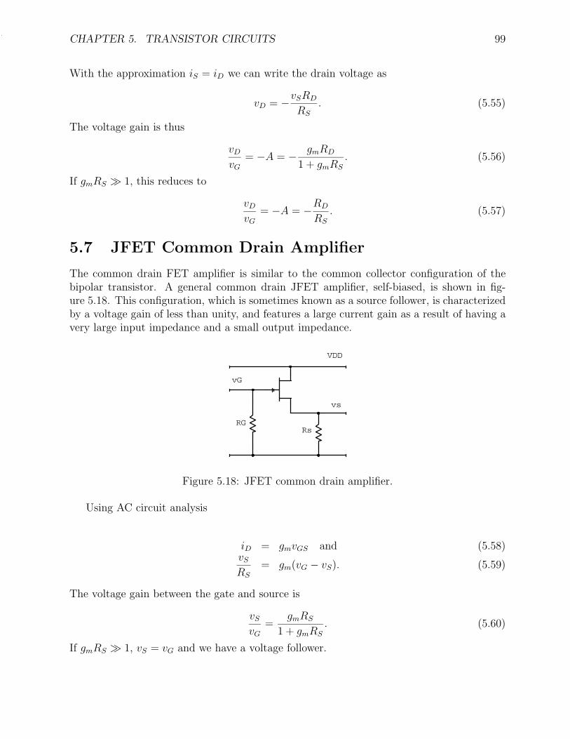
CHAPTER 5. TRANSISTOR CIRCUITS 99
With the approximation iS = iD we can write the drain voltage as
vD = −vSRD
RS
. (5.55)
The voltage gain is thus
vD
vG
= −A = − gmRD
1 + gmRS
. (5.56)
If gmRS 1, this reduces to
vD
vG
= −A = −RD
RS
. (5.57)
5.7 JFET Common Drain Amplifier
The common drain FET amplifier is similar to the common collector configuration of thebipolar transistor. A general common drain JFET amplifier, self-biased, is shown in fig-ure 5.18. This configuration, which is sometimes known as a source follower, is characterizedby a voltage gain of less than unity, and features a large current gain as a result of having avery large input impedance and a small output impedance.
RsRG
vG
vs
VDD
Figure 5.18: JFET common drain amplifier.
Using AC circuit analysis
iD = gmvGS and (5.58)vS
RS
= gm(vG − vS). (5.59)
The voltage gain between the gate and source is
vS
vG
=gmRS
1 + gmRS
. (5.60)
If gmRS 1, vS = vG and we have a voltage follower.
CHAPTER 5. TRANSISTOR CIRCUITS 100
5.8 The Insulated-Gate Field Effect Transistor
The insulated-gate FET, also known as a metal oxide semiconductor field effect transistor(MOSFET), is similar to the JFET but exhibits an even larger resistive input impedance dueto the thin layer of silicon dioxide that is used to insulate the gate from the semiconductorchannel. This insulating layer forms a capacitive coupling between the gate and the bodyof the transistor. The consequent lack of an internal DC connection to the gate makes thedevice more versatile than the JFET, but it also means that the insulating material of thecapacitor can be easily damaged by the internal discharge of static charge developed duringnormal handling.
The MOSFET is widely used in large-scale digital integrated circuits where its high inputimpedance can result in very low power consumption per component. Many of these circuitsfeature bipolar transistor connections to the external terminals, thereby making the devicesless susceptible to damage.
The MOSFET comes in four basic types, N-channel, P-channel, depletion and enhance-ment. The configuration of an N-channel, depletion MOSFET is shown in figure 5.19a. Itsoperation is similar to the N-channel JFET discussed previously: a negative voltage placedon the gate generates a charge depleted region in the N-type material next to the gate,thereby reducing the area of the conduction channel between the drain and source. How-ever, the mechanism by which the depletion region is formed is different from the JFET. Asthe gate is made negative with respect to the source, more positive carriers from the P-typematerial are drawn into the N-channel, where they combine with and eliminate the freenegative charges. This action enlarges the depletion region towards the gate, reducing thearea of the N-channel and thereby lowering the conductivity between the drain and source.For negative applied gate-source voltages the observed effect is much like a JFET, and gm
is also about the same size.However, since the MOSFET gate is insulated from the channel, positive gate-source
voltages may also be applied without losing the FET effect. Depending on the constructiondetails, the application of a positive gate-source voltage to a depletion-type MOSFET canrepel the minority positive carriers in the depleted portion of the N-channel back into the P-type material as discussed below, thereby enlarging the channel and reducing the resistance.If the device exhibits this behaviour, it is known as an enhancement-depletion MOSFET.
A strictly enhancement MOSFET results from the configuration shown in figure 5.19b.Below some threshold of positive gate-source voltage, the connecting channel of N-type ma-terial between the drain and source is completely blocked by the depletion region generatedby the PN junction. As the gate-source voltage is made more positive, the minority positivecarriers are repelled back into the P-type material, leaving free negative charges behind. Theeffect is to shrink the depletion region and increase the conductivity between the drain andsource.
5.9 Power MOSFET Circuits
Traditionally, MOSFET devices have had the drain-to-source current confined to a thin pla-nar volume of silicon lying parallel to the gate. The limited cross-sectional area of material
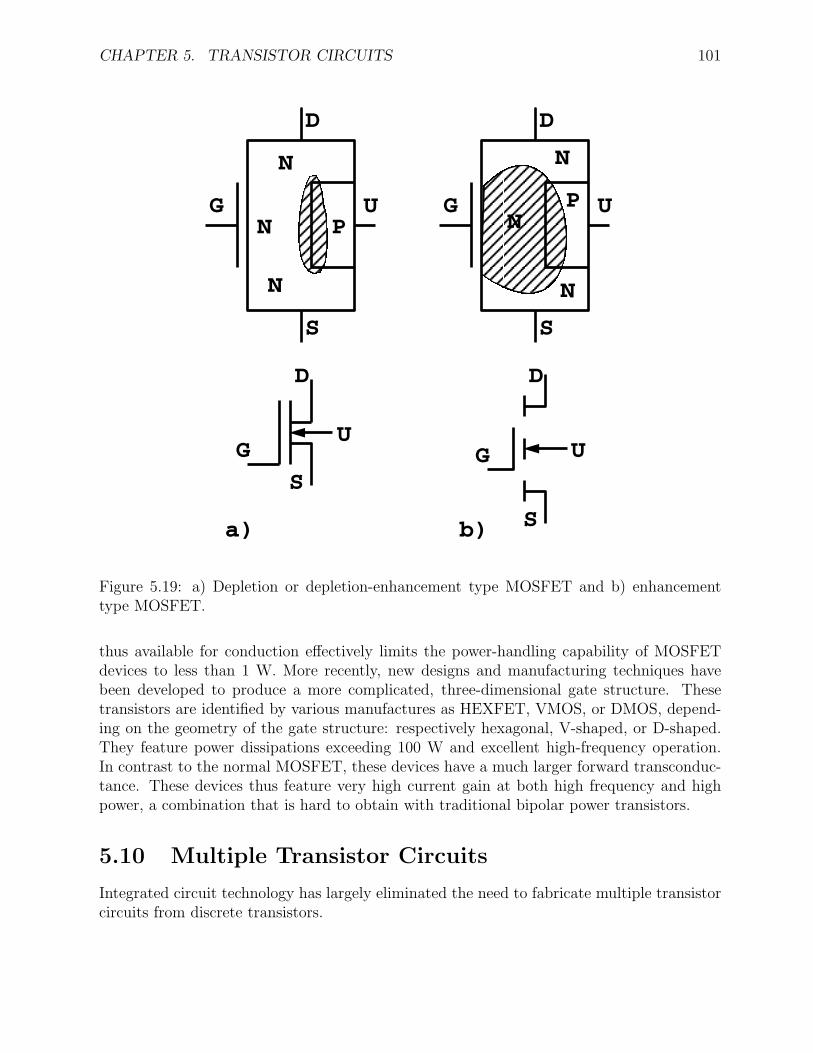
CHAPTER 5. TRANSISTOR CIRCUITS 101
G
D
S
N
N
N
PU G
D
S
U
N
N
NP
G
D
U
S
D
U
SG
a) b)
Figure 5.19: a) Depletion or depletion-enhancement type MOSFET and b) enhancementtype MOSFET.
thus available for conduction effectively limits the power-handling capability of MOSFETdevices to less than 1 W. More recently, new designs and manufacturing techniques havebeen developed to produce a more complicated, three-dimensional gate structure. Thesetransistors are identified by various manufactures as HEXFET, VMOS, or DMOS, depend-ing on the geometry of the gate structure: respectively hexagonal, V-shaped, or D-shaped.They feature power dissipations exceeding 100 W and excellent high-frequency operation.In contrast to the normal MOSFET, these devices have a much larger forward transconduc-tance. These devices thus feature very high current gain at both high frequency and highpower, a combination that is hard to obtain with traditional bipolar power transistors.
5.10 Multiple Transistor Circuits
Integrated circuit technology has largely eliminated the need to fabricate multiple transistorcircuits from discrete transistors.
CHAPTER 5. TRANSISTOR CIRCUITS 102
5.10.1 Coupling Between Single Transistor Stages
Quite often the single-transistor amplifier discussed in the previous lectures does not provideenough gain for an application, or more often, it does not combine gain with the desired inputand output impedance characteristics. Perhaps the most obvious solution (but generally notthe best) is to connect several single-transistor amplifiers, or stages, in tandem one afterthe other. Because of DC biasing considerations, it is usually not practical to connect theoutput of one stage directly to the input of another; some kind of coupling device must beused that permits a change in the DC level between two stages.
A possible circuit features capacitor coupling between single-transistor stages. The inter-stage coupling capacitor allows the following transistor to be DC biased without concern forthe DC component of the driving signal. Thus the DC analysis of the two transistor stagesis separated into two distinct problems.
5.10.2 Darlington and Sziklai Connections
Two bipolar transistors in either the Darlington or Sziklai connection can be used as a single,high gain, transistor. These circuits have AC current gains on the order of h2
fe, providinghigh amplification in a single stage.
The arrangement of two NPN transistors shown in figure 5.20a is known as the Darlingtonconnection. The three unconnected terminals, the base of Q1 and the collector and emitterof Q2, behave like a single transistor with current gain hfe1hfe2 and an overall base to emitterDC voltage drop of 2VPN . Two transistors in the Darlington connection can be purchasedin a single three-terminal package.
A similar circuit result can be obtained with the Sziklai connection of figure 5.20b.Because it uses one transistor of each polarity (NPN and PNP), this connection is alsoknown as the complementary Darlington. The combination again results in a three-terminaldevice that behaves like a single high-current-gain transistor. The overall circuit behaveslike a transistor of the same polarity as Q1.
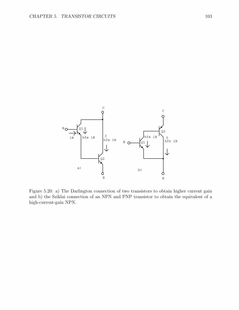
CHAPTER 5. TRANSISTOR CIRCUITS 103
22
b)
hfe iBhfe iB
Q2
Q1
C
E
B
a)
iBhfe iB
hfe iB
Q2
Q1B
E
C
Figure 5.20: a) The Darlington connection of two transistors to obtain higher current gainand b) the Sziklai connection of an NPN and PNP transistor to obtain the equivalent of ahigh-current-gain NPN.
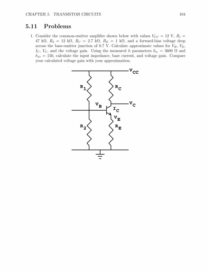
CHAPTER 5. TRANSISTOR CIRCUITS 104
5.11 Problems
1. Consider the common-emitter amplifier shown below with values VCC = 12 V, R1 =47 kΩ, R2 = 12 kΩ, RC = 2.7 kΩ, RE = 1 kΩ, and a forward-bias voltage dropacross the base-emitter junction of 0.7 V. Calculate approximate values for VB, VE,IC , VC , and the voltage gain. Using the measured h parameters hie = 3600 Ω andhfe = 150, calculate the input impedance, base current, and voltage gain. Compareyour calculated voltage gain with your approximation.
IC
EV
VCC
BV CV
CR
ER2R
1R
Chapter 6
Operational Amplifiers
The operational amplifier (op-amp) was designed to perform mathematical operations. Al-though now superseded by the digital computer, op-amps are a common feature of modernanalog electronics.
The op-amp is constructed from several transistor stages, which commonly include adifferential-input stage, an intermediate-gain stage and a push-pull output stage. The dif-ferential amplifier consists of a matched pair of bipolar transistors or FETs. The push-pullamplifier transmits a large current to the load and hence has a small output impedance.
The op-amp is a linear amplifier with Vout ∝ Vin. The DC open-loop voltage gain of atypical op-amp is 103 to 106. The gain is so large that most often feedback is used to obtaina specific transfer function and control the stability.
Cheap IC versions of operational amplifiers are readily available, making their use popularin any analog circuit. The cheap models operate from DC to about 20 kHz, while the high-performance models operate up to 50 MHz. A popular device is the 741 op-amp which dropsoff 6 dB/octave above 5 Hz. Op-amps are usually available as an IC in an 8-pin dual, in-linepackage (DIP). Some op-amp ICs have more than one op-amp on the same chip.
Before proceeding we define a few terms:
linear amplifier – the output is directly proportional to the amplitude of input signal.
open-loop gain, A – the voltage gain without feedback (≈ 105).
closed-loop gain, G – the voltage gain with negative feedback (approximation to H(jω)).
negative feedback – the output is connected to the inverting input forming a feedbackloop (usually through a feedback resistor RF ).
6.1 Open-Loop Amplifiers
Figure 6.1a shows a complete diagram of an operational amplifier. A more common version ofthe diagram is shown in figure 6.1b, where missing parts are assumed to exist. The invertinginput means that the output signal will be 1800 out of phase with the input applied to thisterminal. On the diagram V++ ≡ +VCC = +15 V (DC) and V−− ≡ −VCC = −15 V (DC).
105
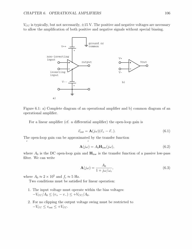
CHAPTER 6. OPERATIONAL AMPLIFIERS 106
VCC is typically, but not necessarily, ±15 V. The positive and negative voltages are necessaryto allow the amplification of both positive and negative signals without special biasing.
V--
+b)
a)
invertinginput
non-invertinginput
+
V++ground orcommon
output Vout
V-
V+
Figure 6.1: a) Complete diagram of an operational amplifier and b) common diagram of anoperational amplifier.
For a linear amplifier (cf. a differential amplifier) the open-loop gain is
vout = A(jω)(v+ − v−). (6.1)
The open-loop gain can be approximated by the transfer function
A(jω) = A0Hlow(jω), (6.2)
where A0 is the DC open-loop gain and Hlow is the transfer function of a passive low-passfilter. We can write
A(jω) =A0
1 + jω/ωc
, (6.3)
where A0 ≈ 2 × 10⁵ and fc ≈ 5 Hz.Two conditions must be satisfied for linear operation:
1. The input voltage must operate within the bias voltages:−VCC/A0 ≤ (v+ − v−) ≤ +VCC/A0.
2. For no clipping the output voltage swing must be restricted to−VCC ≤ vout ≤ +VCC .
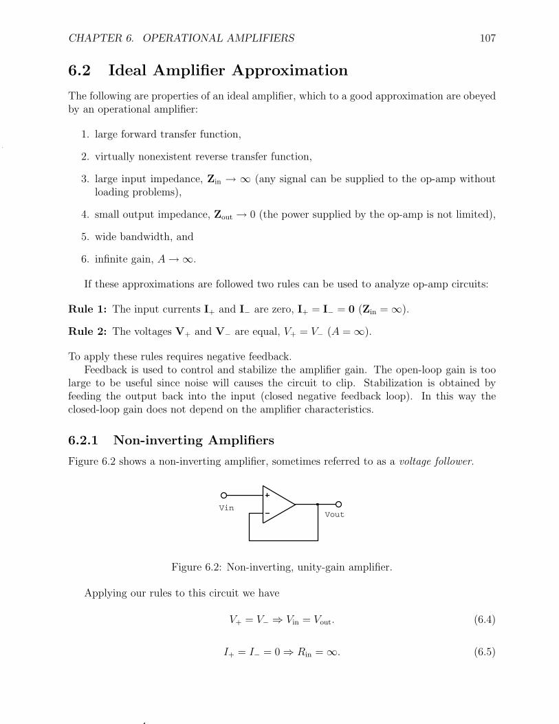
CHAPTER 6. OPERATIONAL AMPLIFIERS 107
6.2 Ideal Amplifier Approximation
The following are properties of an ideal amplifier, which to a good approximation are obeyedby an operational amplifier:
1. large forward transfer function,
2. virtually nonexistent reverse transfer function,
3. large input impedance, Zin → ∞ (any signal can be supplied to the op-amp withoutloading problems),
4. small output impedance, Zout → 0 (the power supplied by the op-amp is not limited),
5. wide bandwidth, and
6. infinite gain, A → ∞.
If these approximations are followed two rules can be used to analyze op-amp circuits:
Rule 1: The input currents I+ and I− are zero, I+ = I− = 0 (Zin = ∞).
Rule 2: The voltages V+ and V− are equal, V+ = V− (A = ∞).
To apply these rules requires negative feedback.Feedback is used to control and stabilize the amplifier gain. The open-loop gain is too
large to be useful since noise will causes the circuit to clip. Stabilization is obtained byfeeding the output back into the input (closed negative feedback loop). In this way theclosed-loop gain does not depend on the amplifier characteristics.
6.2.1 Non-inverting Amplifiers
Figure 6.2 shows a non-inverting amplifier, sometimes referred to as a voltage follower.
VinVout
Figure 6.2: Non-inverting, unity-gain amplifier.
Applying our rules to this circuit we have
V+ = V− ⇒ Vin = Vout. (6.4)
I+ = I− = 0 ⇒ Rin = ∞. (6.5)
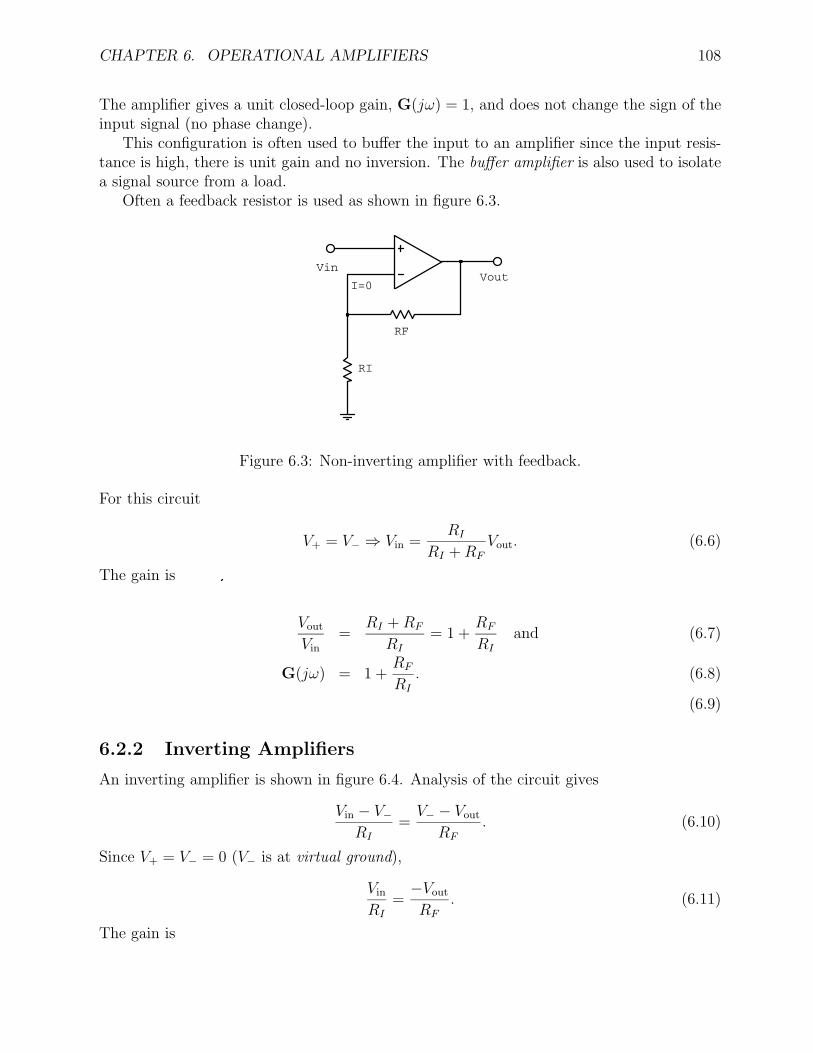
CHAPTER 6. OPERATIONAL AMPLIFIERS 108
The amplifier gives a unit closed-loop gain, G(jω) = 1, and does not change the sign of theinput signal (no phase change).
This configuration is often used to buffer the input to an amplifier since the input resis-tance is high, there is unit gain and no inversion. The buffer amplifier is also used to isolatea signal source from a load.
Often a feedback resistor is used as shown in figure 6.3.
VoutI=0
Vin
RF
RI
Figure 6.3: Non-inverting amplifier with feedback.
For this circuit
V+ = V− ⇒ Vin =RI
RI + RF
Vout. (6.6)
The gain is
Vout
Vin
=RI + RF
RI
= 1 +RF
RI
and (6.7)
G(jω) = 1 +RF
RI
. (6.8)
(6.9)
6.2.2 Inverting Amplifiers
An inverting amplifier is shown in figure 6.4. Analysis of the circuit gives
Vin − V−RI
=V− − Vout
RF
. (6.10)
Since V+ = V− = 0 (V− is at virtual ground),
Vin
RI
=−Vout
RF
. (6.11)
The gain is
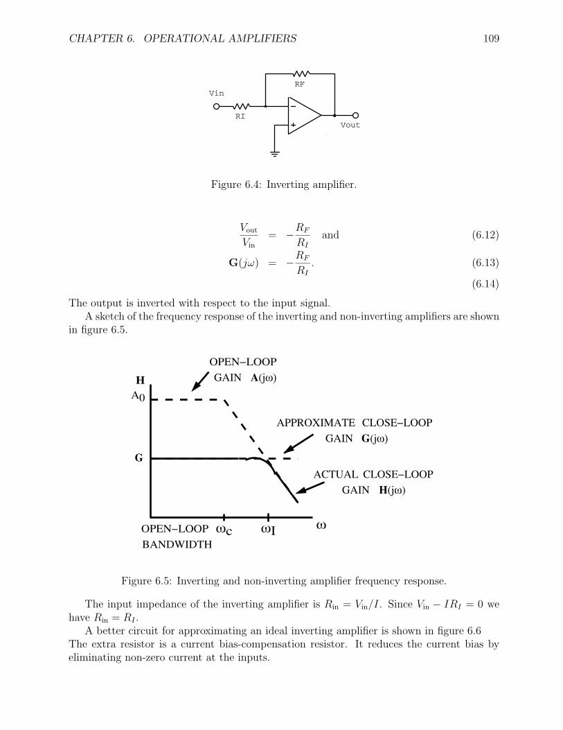
CHAPTER 6. OPERATIONAL AMPLIFIERS 109
RF
RIVout
Vin
Figure 6.4: Inverting amplifier.
Vout
Vin
= −RF
RI
and (6.12)
G(jω) = −RF
RI
. (6.13)
(6.14)
The output is inverted with respect to the input signal.A sketch of the frequency response of the inverting and non-inverting amplifiers are shown
in figure 6.5.
OPEN−LOOP
GAIN A(jω)
APPROXIMATE CLOSE−LOOP
GAIN G(jω)
ACTUAL CLOSE−LOOP
GAIN H(jω)
OPEN−LOOP
BANDWIDTH
H
G
A0
ωc ωωΙ
Figure 6.5: Inverting and non-inverting amplifier frequency response.
The input impedance of the inverting amplifier is Rin = Vin/I. Since Vin − IRI = 0 wehave Rin = RI .
A better circuit for approximating an ideal inverting amplifier is shown in figure 6.6The extra resistor is a current bias-compensation resistor. It reduces the current bias byeliminating non-zero current at the inputs.
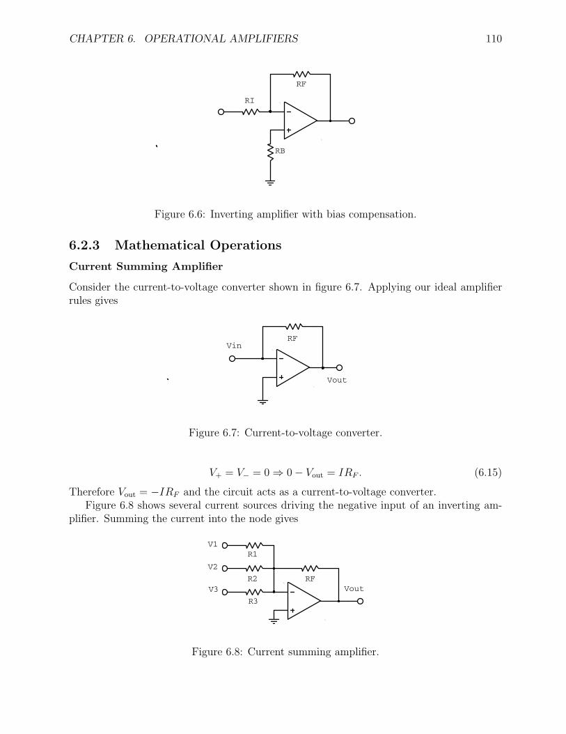
CHAPTER 6. OPERATIONAL AMPLIFIERS 110
RB
RF
RI
Figure 6.6: Inverting amplifier with bias compensation.
6.2.3 Mathematical Operations
Current Summing Amplifier
Consider the current-to-voltage converter shown in figure 6.7. Applying our ideal amplifierrules gives
RF
Vout
Vin
Figure 6.7: Current-to-voltage converter.
V+ = V− = 0 ⇒ 0 − Vout = IRF . (6.15)
Therefore Vout = −IRF and the circuit acts as a current-to-voltage converter.Figure 6.8 shows several current sources driving the negative input of an inverting am-
plifier. Summing the current into the node gives
RF
R3
R2
R1
V3
V2
V1
Vout
Figure 6.8: Current summing amplifier.
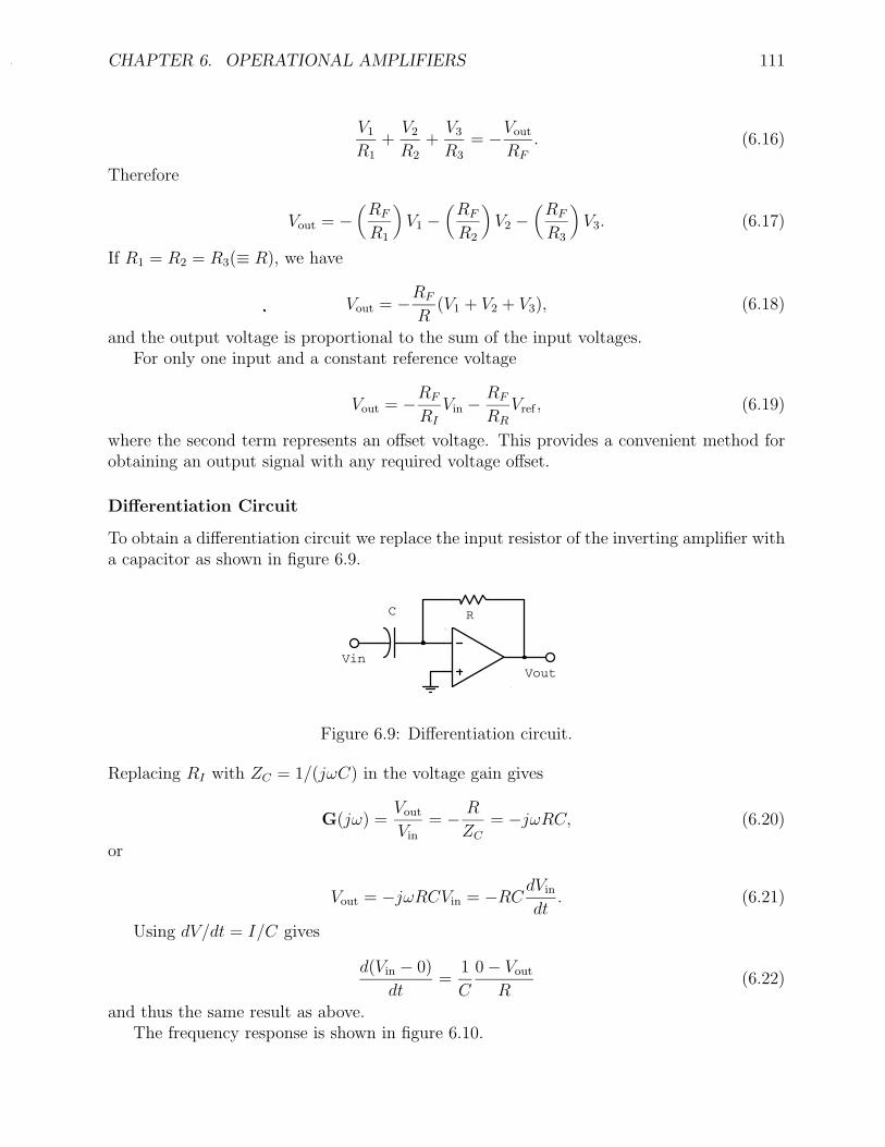
CHAPTER 6. OPERATIONAL AMPLIFIERS 111
V1
R1
+V2
R2
+V3
R3
= −Vout
RF
. (6.16)
Therefore
Vout = −(
RF
R1
)V1 −
(RF
R2
)V2 −
(RF
R3
)V3. (6.17)
If R1 = R2 = R3(≡ R), we have
Vout = −RF
R(V1 + V2 + V3), (6.18)
and the output voltage is proportional to the sum of the input voltages.For only one input and a constant reference voltage
Vout = −RF
RI
Vin − RF
RR
Vref , (6.19)
where the second term represents an offset voltage. This provides a convenient method forobtaining an output signal with any required voltage offset.
Differentiation Circuit
To obtain a differentiation circuit we replace the input resistor of the inverting amplifier witha capacitor as shown in figure 6.9.
C
VinVout
R
Figure 6.9: Differentiation circuit.
Replacing RI with ZC = 1/(jωC) in the voltage gain gives
G(jω) =Vout
Vin
= − R
ZC
= −jωRC, (6.20)
or
Vout = −jωRCVin = −RCdVin
dt. (6.21)
Using dV/dt = I/C gives
d(Vin − 0)
dt=
1
C
0 − Vout
R(6.22)
and thus the same result as above.The frequency response is shown in figure 6.10.
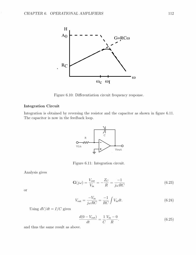
CHAPTER 6. OPERATIONAL AMPLIFIERS 112
H
A0
RC
ωωc ωI
G=RCω
Figure 6.10: Differentiation circuit frequency response.
Integration Circuit
Integration is obtained by reversing the resistor and the capacitor as shown in figure 6.11.The capacitor is now in the feedback loop.
CR
VinVout
Figure 6.11: Integration circuit.
Analysis gives
G(jω) =Vout
Vin
= −ZC
R=
−1
jωRC(6.23)
or
Vout =−Vin
jωRC=
−1
RC
∫Vindt. (6.24)
Using dV/dt = I/C gives
d(0 − Vout)
dt=
1
C
Vin − 0
R. (6.25)
and thus the same result as above.
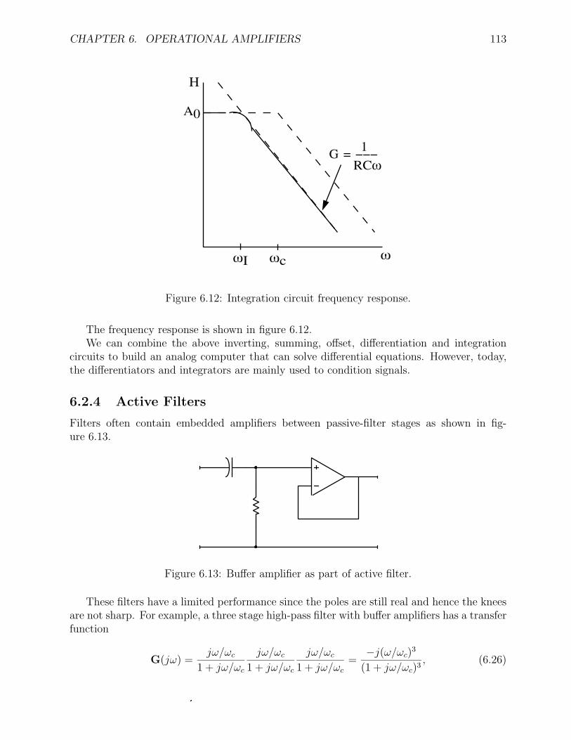
CHAPTER 6. OPERATIONAL AMPLIFIERS 113
Η
A0
G = −−−1
RCω
ωωcωI
Figure 6.12: Integration circuit frequency response.
The frequency response is shown in figure 6.12.We can combine the above inverting, summing, offset, differentiation and integration
circuits to build an analog computer that can solve differential equations. However, today,the differentiators and integrators are mainly used to condition signals.
6.2.4 Active Filters
Filters often contain embedded amplifiers between passive-filter stages as shown in fig-ure 6.13.
Figure 6.13: Buffer amplifier as part of active filter.
These filters have a limited performance since the poles are still real and hence the kneesare not sharp. For example, a three stage high-pass filter with buffer amplifiers has a transferfunction
G(jω) =jω/ωc
1 + jω/ωc
jω/ωc
1 + jω/ωc
jω/ωc
1 + jω/ωc
=−j(ω/ωc)
3
(1 + jω/ωc)3, (6.26)
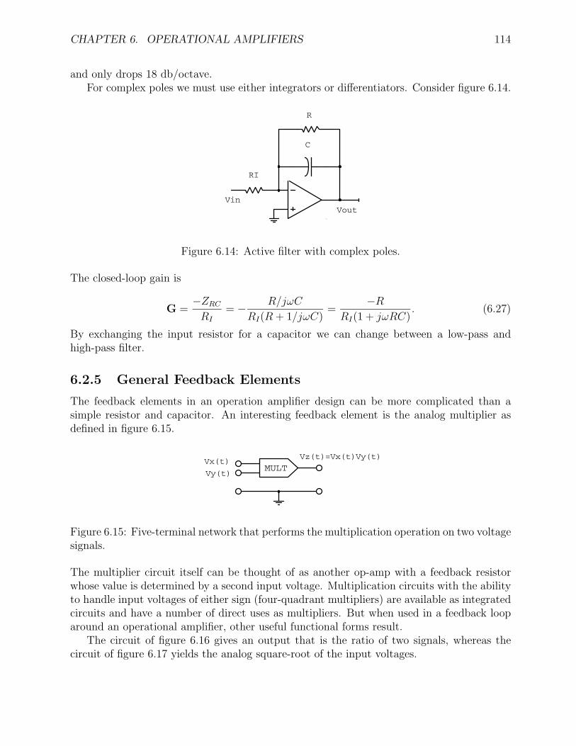
CHAPTER 6. OPERATIONAL AMPLIFIERS 114
and only drops 18 db/octave.For complex poles we must use either integrators or differentiators. Consider figure 6.14.
C
R
RI
VinVout
Figure 6.14: Active filter with complex poles.
The closed-loop gain is
G =−ZRC
RI
= − R/jωC
RI(R + 1/jωC)=
−R
RI(1 + jωRC). (6.27)
By exchanging the input resistor for a capacitor we can change between a low-pass andhigh-pass filter.
6.2.5 General Feedback Elements
The feedback elements in an operation amplifier design can be more complicated than asimple resistor and capacitor. An interesting feedback element is the analog multiplier asdefined in figure 6.15.
Vy(t)
Vx(t)Vz(t)=Vx(t)Vy(t)
MULT
Figure 6.15: Five-terminal network that performs the multiplication operation on two voltagesignals.
The multiplier circuit itself can be thought of as another op-amp with a feedback resistorwhose value is determined by a second input voltage. Multiplication circuits with the abilityto handle input voltages of either sign (four-quadrant multipliers) are available as integratedcircuits and have a number of direct uses as multipliers. But when used in a feedback looparound an operational amplifier, other useful functional forms result.
The circuit of figure 6.16 gives an output that is the ratio of two signals, whereas thecircuit of figure 6.17 yields the analog square-root of the input voltages.
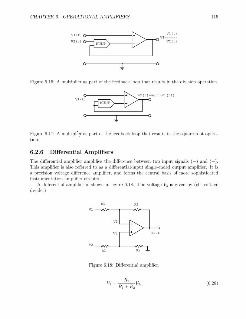
CHAPTER 6. OPERATIONAL AMPLIFIERS 115
V1(t)V3=----- V2(t)V2(t)
V1(t)
MULT
Figure 6.16: A multiplier as part of the feedback loop that results in the division operation.
v2(t)=sqrt(v1(t))V1(t)
MULT
Figure 6.17: A multiplier as part of the feedback loop that results in the square-root opera-tion.
6.2.6 Differential Amplifiers
The differential amplifier amplifies the difference between two input signals (−) and (+).This amplifier is also referred to as a differential-input single-ended output amplifier. It isa precision voltage difference amplifier, and forms the central basis of more sophisticatedinstrumentation amplifier circuits.
A differential amplifier is shown in figure 6.18. The voltage V3 is given by (cf. voltagedivider)
V3
V3
R2R1
R2R1
Vout
V2
V1
Figure 6.18: Differential amplifier.
V3 =R2
R1 + R2
V2, (6.28)
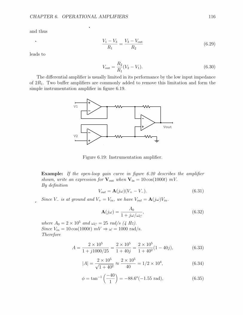
CHAPTER 6. OPERATIONAL AMPLIFIERS 116
and thus
V1 − V3
R1
=V3 − Vout
R2
(6.29)
leads to
Vout =R2
R1
(V2 − V1). (6.30)
The differential amplifier is usually limited in its performance by the low input impedanceof 2R1. Two buffer amplifiers are commonly added to remove this limitation and form thesimple instrumentation amplifier in figure 6.19.
Vout
V2
V1
Figure 6.19: Instrumentation amplifier.
Example: If the open-loop gain curve in figure 6.20 describes the amplifiershown, write an expression for Vout when Vin = 10 cos(1000t) mV.By definition
Vout = A(jω)(V+ − V−). (6.31)
Since V− is at ground and V+ = Vin, we have Vout = A(jω)Vin.
A(jω) =A0
1 + jω/ωC
, (6.32)
where A0 = 2 × 10⁵ and ωC = 25 rad/s (4 Hz).Since Vin = 10 cos(1000t) mV ⇒ ω = 1000 rad/s.Therefore
A =2 × 10⁵
1 + j1000/25=
2 × 10⁵
1 + 40j=
2 × 10⁵
1 + 402(1 − 40j), (6.33)
|A| =2 × 10⁵
√1 + 402
≈ 2 × 10⁵
40= 1/2 × 104, (6.34)
φ = tan−1(−40
1
)= −88.6o(−1.55 rad), (6.35)
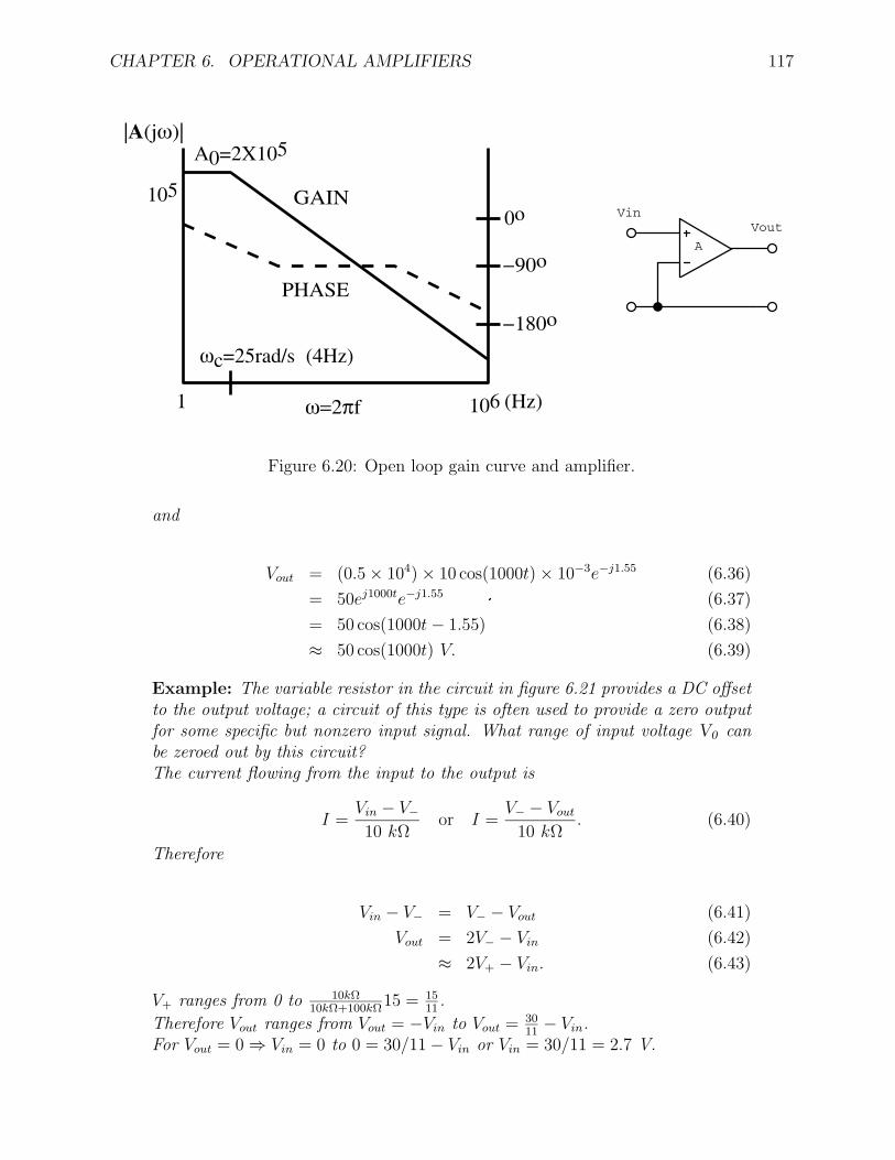
CHAPTER 6. OPERATIONAL AMPLIFIERS 117
1 106 (Hz)
105
|A(jω)|A0=2X10⁵
ωc=25rad/s (4Hz)
ω=2πf
GAIN
PHASE
0o
−90o
−180o
VoutVin
A
Figure 6.20: Open loop gain curve and amplifier.
and
Vout = (0.5 × 104) × 10 cos(1000t) × 10−3e−j1.55 (6.36)
= 50ej1000te−j1.55 (6.37)
= 50 cos(1000t − 1.55) (6.38)
≈ 50 cos(1000t) V. (6.39)
Example: The variable resistor in the circuit in figure 6.21 provides a DC offsetto the output voltage; a circuit of this type is often used to provide a zero outputfor some specific but nonzero input signal. What range of input voltage V0 canbe zeroed out by this circuit?The current flowing from the input to the output is
I =Vin − V−10 kΩ
or I =V− − Vout
10 kΩ. (6.40)
Therefore
Vin − V− = V− − Vout (6.41)
Vout = 2V− − Vin (6.42)
≈ 2V+ − Vin. (6.43)
V+ ranges from 0 to 10kΩ10kΩ+100kΩ
15 = 1511
.
Therefore Vout ranges from Vout = −Vin to Vout = 3011
− Vin.For Vout = 0 ⇒ Vin = 0 to 0 = 30/11 − Vin or Vin = 30/11 = 2.7 V.
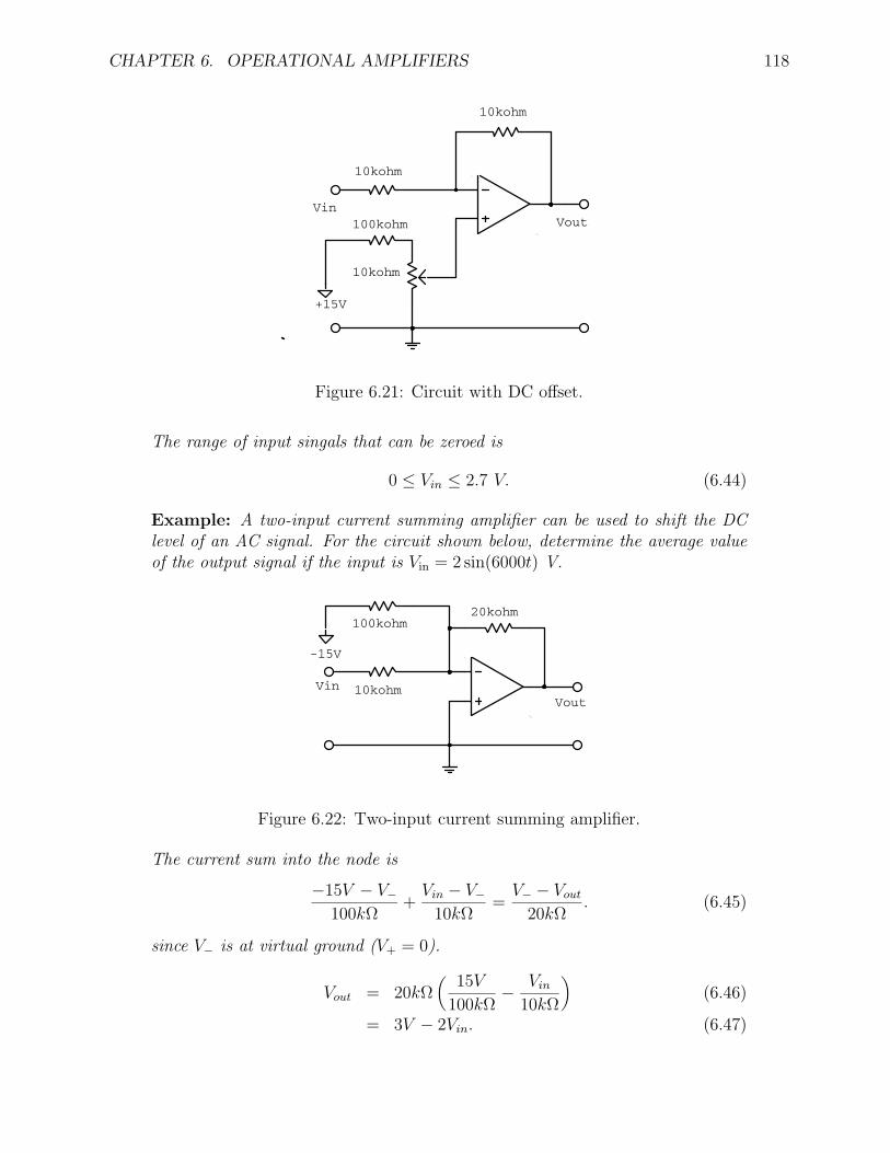
CHAPTER 6. OPERATIONAL AMPLIFIERS 118
10kohm
100kohm
10kohm
VinVout
10kohm
+15V
Figure 6.21: Circuit with DC offset.
The range of input singals that can be zeroed is
0 ≤ Vin ≤ 2.7 V. (6.44)
Example: A two-input current summing amplifier can be used to shift the DClevel of an AC signal. For the circuit shown below, determine the average valueof the output signal if the input is Vin = 2 sin(6000t) V.
20kohm
10kohm
100kohm
VinVout
-15V
Figure 6.22: Two-input current summing amplifier.
The current sum into the node is
−15V − V−100kΩ
+Vin − V−
10kΩ=
V− − Vout
20kΩ. (6.45)
since V− is at virtual ground (V+ = 0).
Vout = 20kΩ(
15V
100kΩ− Vin
10kΩ
)(6.46)
= 3V − 2Vin. (6.47)
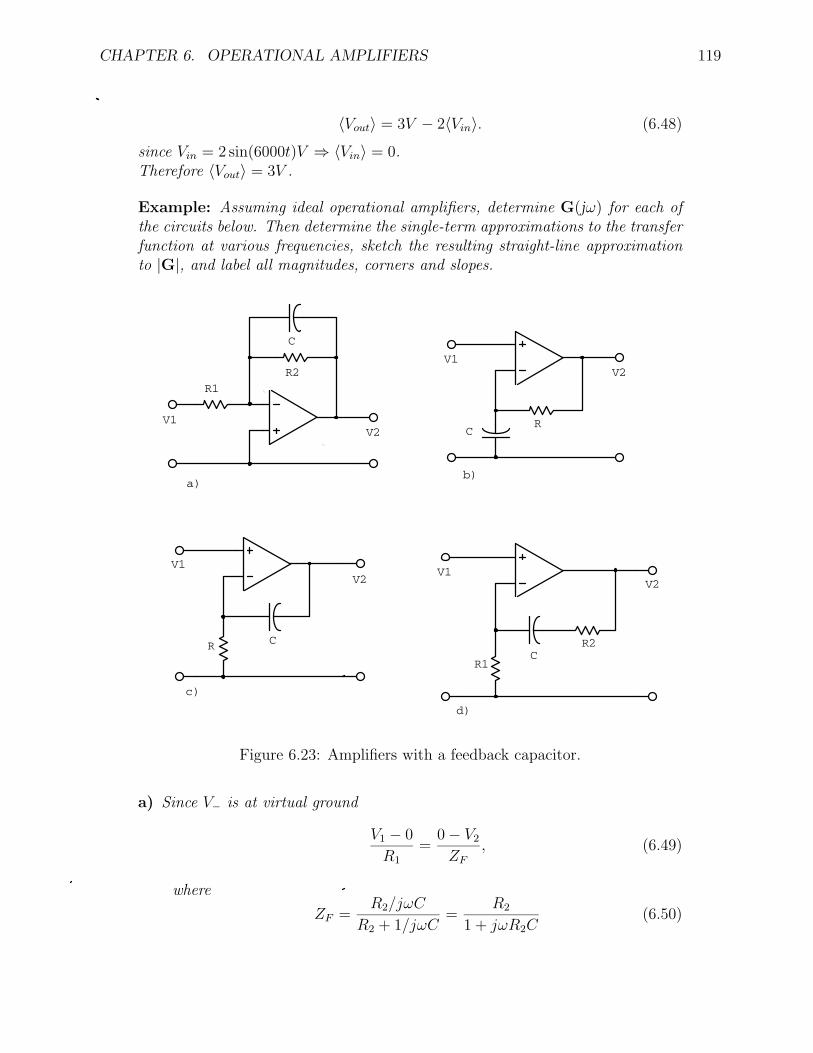
CHAPTER 6. OPERATIONAL AMPLIFIERS 119
〈Vout〉 = 3V − 2〈Vin〉. (6.48)
since Vin = 2 sin(6000t)V ⇒ 〈Vin〉 = 0.Therefore 〈Vout〉 = 3V .
Example: Assuming ideal operational amplifiers, determine G(jω) for each ofthe circuits below. Then determine the single-term approximations to the transferfunction at various frequencies, sketch the resulting straight-line approximationto |G|, and label all magnitudes, corners and slopes.
C
d)
c)
b)a)
CRC
R2
R1
R
C
R2
R1
V2V1
V2V1
V2V1
V2V1
Figure 6.23: Amplifiers with a feedback capacitor.
a) Since V− is at virtual ground
V1 − 0
R1
=0 − V2
ZF
, (6.49)
where
ZF =R2/jωC
R2 + 1/jωC=
R2
1 + jωR2C(6.50)
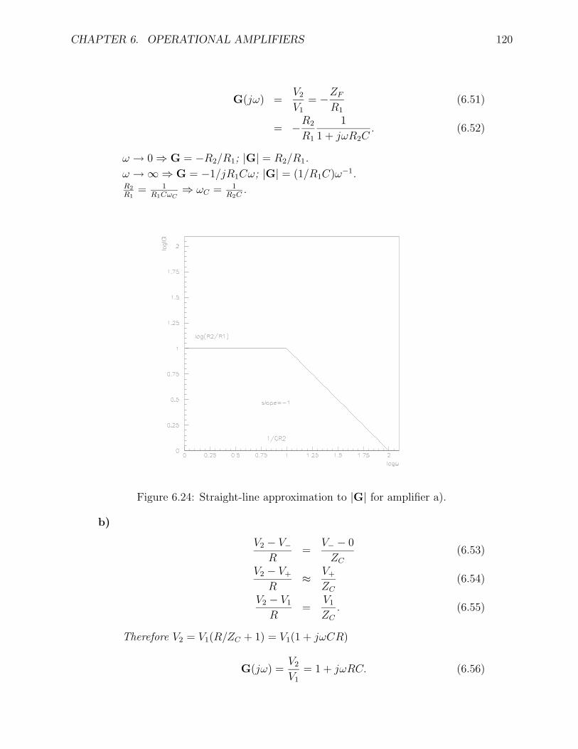
CHAPTER 6. OPERATIONAL AMPLIFIERS 120
G(jω) =V2
V1
= −ZF
R1
(6.51)
= −R2
R1
1
1 + jωR2C. (6.52)
ω → 0 ⇒ G = −R2/R1; |G| = R2/R1.
ω → ∞ ⇒ G = −1/jR1Cω; |G| = (1/R1C)ω−1.R2
R1= 1
R1CωC⇒ ωC = 1
R2C.
Figure 6.24: Straight-line approximation to |G| for amplifier a).
b)
V2 − V−R
=V− − 0
ZC
(6.53)
V2 − V+
R≈ V+
ZC
(6.54)
V2 − V1
R=
V1
ZC
. (6.55)
Therefore V2 = V1(R/ZC + 1) = V1(1 + jωCR)
G(jω) =V2
V1
= 1 + jωRC. (6.56)
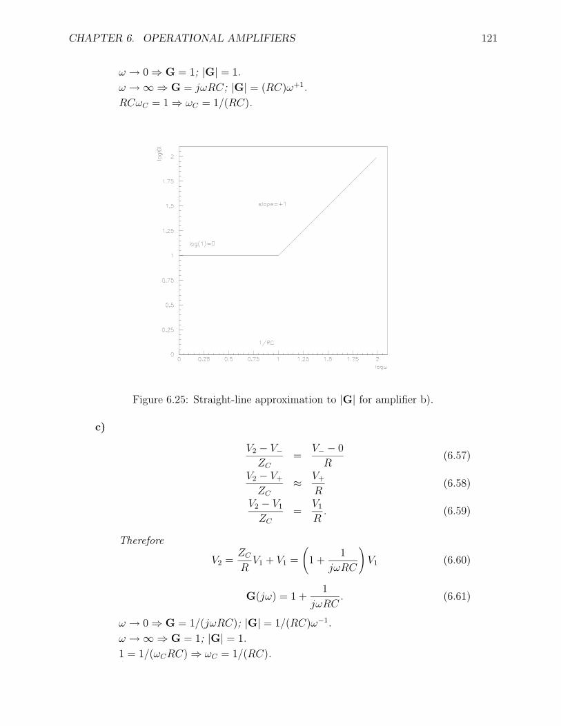
CHAPTER 6. OPERATIONAL AMPLIFIERS 121
ω → 0 ⇒ G = 1; |G| = 1.
ω → ∞ ⇒ G = jωRC; |G| = (RC)ω+1.
RCωC = 1 ⇒ ωC = 1/(RC).
Figure 6.25: Straight-line approximation to |G| for amplifier b).
c)
V2 − V−ZC
=V− − 0
R(6.57)
V2 − V+
ZC
≈ V+
R(6.58)
V2 − V1
ZC
=V1
R. (6.59)
Therefore
V2 =ZC
RV1 + V1 =
(1 +
1
jωRC
)V1 (6.60)
G(jω) = 1 +1
jωRC. (6.61)
ω → 0 ⇒ G = 1/(jωRC); |G| = 1/(RC)ω−1.
ω → ∞ ⇒ G = 1; |G| = 1.
1 = 1/(ωCRC) ⇒ ωC = 1/(RC).
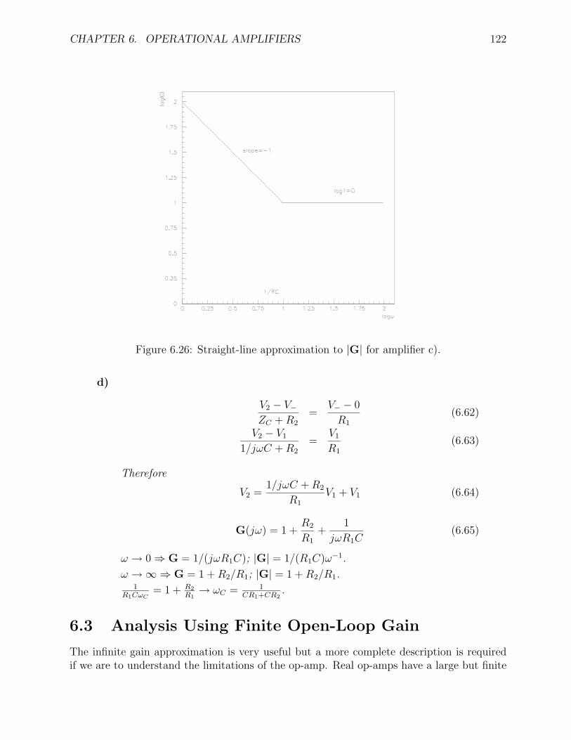
CHAPTER 6. OPERATIONAL AMPLIFIERS 122
Figure 6.26: Straight-line approximation to |G| for amplifier c).
d)
V2 − V−ZC + R2
=V− − 0
R1
(6.62)
V2 − V1
1/jωC + R2
=V1
R1
(6.63)
Therefore
V2 =1/jωC + R2
R1
V1 + V1 (6.64)
G(jω) = 1 +R2
R1
+1
jωR1C(6.65)
ω → 0 ⇒ G = 1/(jωR1C); |G| = 1/(R1C)ω−1.
ω → ∞ ⇒ G = 1 + R2/R1; |G| = 1 + R2/R1.1
R1CωC= 1 + R2
R1→ ωC = 1
CR1+CR2.
6.3 Analysis Using Finite Open-Loop Gain
The infinite gain approximation is very useful but a more complete description is requiredif we are to understand the limitations of the op-amp. Real op-amps have a large but finite
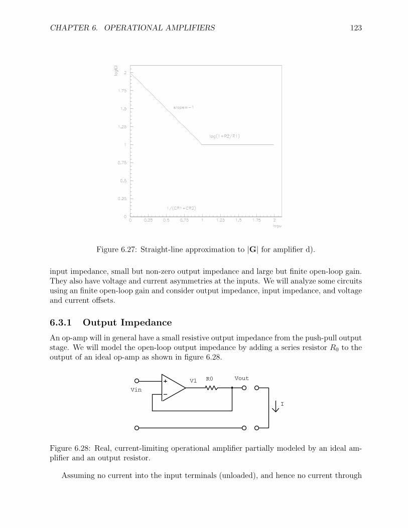
CHAPTER 6. OPERATIONAL AMPLIFIERS 123
Figure 6.27: Straight-line approximation to |G| for amplifier d).
input impedance, small but non-zero output impedance and large but finite open-loop gain.They also have voltage and current asymmetries at the inputs. We will analyze some circuitsusing an finite open-loop gain and consider output impedance, input impedance, and voltageand current offsets.
6.3.1 Output Impedance
An op-amp will in general have a small resistive output impedance from the push-pull outputstage. We will model the open-loop output impedance by adding a series resistor R0 to theoutput of an ideal op-amp as shown in figure 6.28.
I
VoutR0V1
Vin
Figure 6.28: Real, current-limiting operational amplifier partially modeled by an ideal am-plifier and an output resistor.
Assuming no current into the input terminals (unloaded), and hence no current through
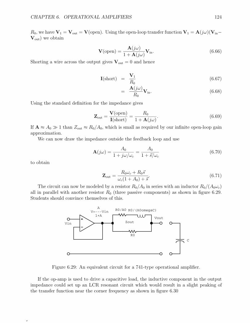
CHAPTER 6. OPERATIONAL AMPLIFIERS 124
R0, we have V1 = Vout = V(open). Using the open-loop transfer function V1 = A(jω)(Vin−Vout) we obtain
V(open) =A(jω)
1 + A(jω)Vin. (6.66)
Shorting a wire across the output gives Vout = 0 and hence
I(short) =V1
R0
(6.67)
=A(jω)
R0
Vin. (6.68)
Using the standard definition for the impedance gives
Zout =V(open)
I(short)=
R0
1 + A(jω). (6.69)
If A ≈ A0 1 than Zout ≈ R0/A0, which is small as required by our infinite open-loop gainapproximation.
We can now draw the impedance outside the feedback loop and use
A(jω) =A0
1 + jω/ωc
=A0
1 + s/ωc
(6.70)
to obtain
Zout =R0ωc + R0s
ωc(1 + A0) + s. (6.71)
The circuit can now be modeled by a resistor R0/A0 in series with an inductor R0/(A0ωc)all in parallel with another resistor R0 (three passive components) as shown in figure 6.29.Students should convince themselves of this.
R0/(A0omegaC) AV=---Vin 1+A
Zout
R0/A0
R0
Vout
Vin
C
Figure 6.29: An equivalent circuit for a 741-type operational amplifier.
If the op-amp is used to drive a capacitive load, the inductive component in the outputimpedance could set up an LCR resonant circuit which would result in a slight peaking ofthe transfer function near the corner frequency as shown in figure 6.30
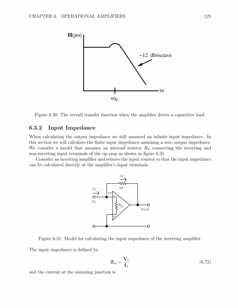
CHAPTER 6. OPERATIONAL AMPLIFIERS 125
H(jω)
ωc
ω
−12 db/octave
Figure 6.30: The overall transfer function when the amplifier drives a capacitive load.
6.3.2 Input Impedance
When calculating the output impedance we still assumed an infinite input impedance. Inthis section we will calculate the finite input impedance assuming a zero output impedance.We consider a model that assumes an internal resistor RT connecting the inverting andnon-inverting input terminals of the op-amp as shown in figure 6.31
Consider an inverting amplifier and remove the input resistor so that the input impedancecan be calculated directly at the amplifier’s input terminals.
V1
ITI1
I2
RF
VoutRT
+
-
Figure 6.31: Model for calculating the input impedance of the inverting amplifier.
The input impedance is defined by
Zin =V1
I1
(6.72)
and the current at the summing junction is
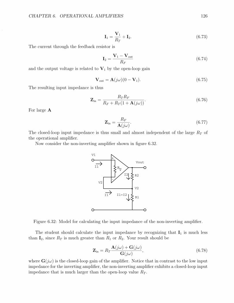
CHAPTER 6. OPERATIONAL AMPLIFIERS 126
I1 =V1
RT
+ I2. (6.73)
The current through the feedback resistor is
I2 =V1 − Vout
RF
(6.74)
and the output voltage is related to V1 by the open-loop gain
Vout = A(jω)(0 − V1). (6.75)
The resulting input impedance is thus
Zin =RT RF
RF + RT (1 + A(jω)). (6.76)
For large A
Zin =RF
A(jω). (6.77)
The closed-loop input impedance is thus small and almost independent of the large RT ofthe operational amplifier.
Now consider the non-inverting amplifier shown in figure 6.32.
I1+I2
V2
R1
R2I2
I1
V2
I1
V1
Vout
RT
+
-
Figure 6.32: Model for calculating the input impedance of the non-inverting amplifier.
The student should calculate the input impedance by recognizing that I1 is much lessthan I2, since RT is much greater than R1 or R2. Your result should be
Zin = RTA(jω) + G(jω)
G(jω), (6.78)
where G(jω) is the closed-loop gain of the amplifier. Notice that in contrast to the low inputimpedance for the inverting amplifier, the non-inverting amplifier exhibits a closed-loop inputimpedance that is much larger than the open-loop value RT .
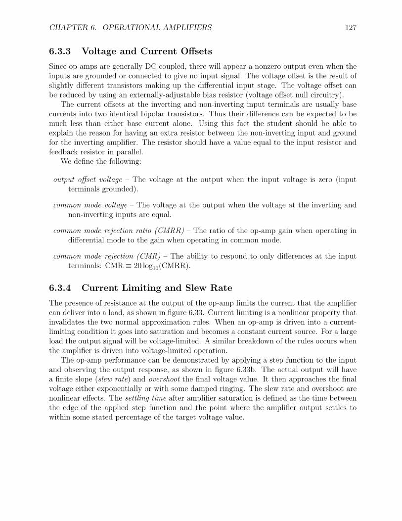
CHAPTER 6. OPERATIONAL AMPLIFIERS 127
6.3.3 Voltage and Current Offsets
Since op-amps are generally DC coupled, there will appear a nonzero output even when theinputs are grounded or connected to give no input signal. The voltage offset is the result ofslightly different transistors making up the differential input stage. The voltage offset canbe reduced by using an externally-adjustable bias resistor (voltage offset null circuitry).
The current offsets at the inverting and non-inverting input terminals are usually basecurrents into two identical bipolar transistors. Thus their difference can be expected to bemuch less than either base current alone. Using this fact the student should be able toexplain the reason for having an extra resistor between the non-inverting input and groundfor the inverting amplifier. The resistor should have a value equal to the input resistor andfeedback resistor in parallel.
We define the following:
output offset voltage – The voltage at the output when the input voltage is zero (inputterminals grounded).
common mode voltage – The voltage at the output when the voltage at the inverting andnon-inverting inputs are equal.
common mode rejection ratio (CMRR) – The ratio of the op-amp gain when operating indifferential mode to the gain when operating in common mode.
common mode rejection (CMR) – The ability to respond to only differences at the inputterminals: CMR ≡ 20 log10(CMRR).
6.3.4 Current Limiting and Slew Rate
The presence of resistance at the output of the op-amp limits the current that the amplifiercan deliver into a load, as shown in figure 6.33. Current limiting is a nonlinear property thatinvalidates the two normal approximation rules. When an op-amp is driven into a current-limiting condition it goes into saturation and becomes a constant current source. For a largeload the output signal will be voltage-limited. A similar breakdown of the rules occurs whenthe amplifier is driven into voltage-limited operation.
The op-amp performance can be demonstrated by applying a step function to the inputand observing the output response, as shown in figure 6.33b. The actual output will havea finite slope (slew rate) and overshoot the final voltage value. It then approaches the finalvoltage either exponentially or with some damped ringing. The slew rate and overshoot arenonlinear effects. The settling time after amplifier saturation is defined as the time betweenthe edge of the applied step function and the point where the amplifier output settles towithin some stated percentage of the target voltage value.
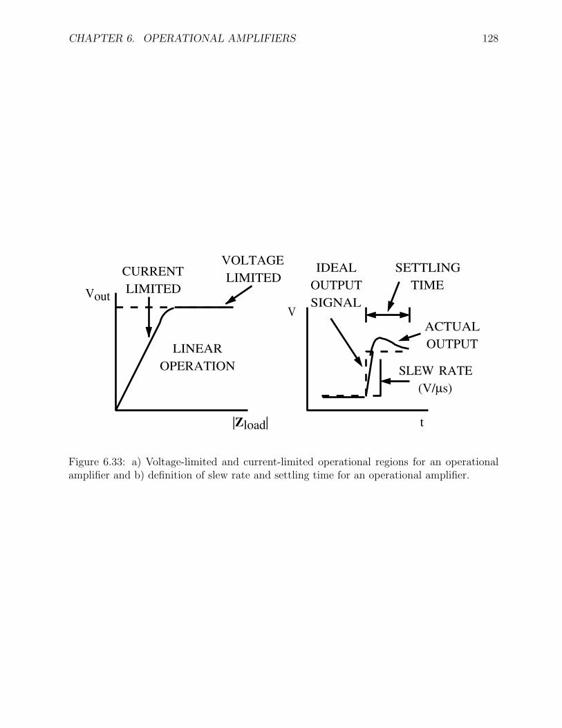
CHAPTER 6. OPERATIONAL AMPLIFIERS 128
Vout
|Zload|
CURRENTLIMITED
VOLTAGELIMITED
LINEAROPERATION
V
t
ACTUALOUTPUT
IDEALOUTPUTSIGNAL
SETTLINGTIME
SLEW RATE(V/µs)
Figure 6.33: a) Voltage-limited and current-limited operational regions for an operationalamplifier and b) definition of slew rate and settling time for an operational amplifier.
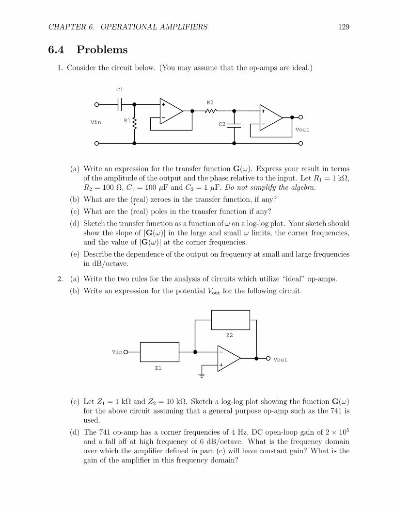
CHAPTER 6. OPERATIONAL AMPLIFIERS 129
6.4 Problems
1. Consider the circuit below. (You may assume that the op-amps are ideal.)
VoutVin
R2
R1C2
C1
(a) Write an expression for the transfer function G(ω). Express your result in termsof the amplitude of the output and the phase relative to the input. Let R1 = 1 kΩ,R2 = 100 Ω, C1 = 100 µF and C2 = 1 µF. Do not simplify the algebra.
(b) What are the (real) zeroes in the transfer function, if any?
(c) What are the (real) poles in the transfer function if any?
(d) Sketch the transfer function as a function of ω on a log-log plot. Your sketch shouldshow the slope of |G(ω)| in the large and small ω limits, the corner frequencies,and the value of |G(ω)| at the corner frequencies.
(e) Describe the dependence of the output on frequency at small and large frequenciesin dB/octave.
2. (a) Write the two rules for the analysis of circuits which utilize “ideal” op-amps.
(b) Write an expression for the potential Vout for the following circuit.
Z1
Z2
Vin
Vout
Z2
Z1
(c) Let Z1 = 1 kΩ and Z2 = 10 kΩ. Sketch a log-log plot showing the function G(ω)for the above circuit assuming that a general purpose op-amp such as the 741 isused.
(d) The 741 op-amp has a corner frequencies of 4 Hz, DC open-loop gain of 2 × 10⁵
and a fall off at high frequency of 6 dB/octave. What is the frequency domainover which the amplifier defined in part (c) will have constant gain? What is thegain of the amplifier in this frequency domain?
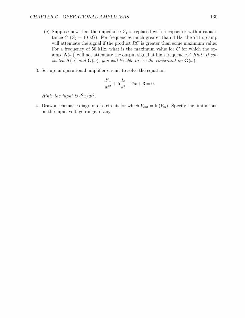
CHAPTER 6. OPERATIONAL AMPLIFIERS 130
(e) Suppose now that the impedance Z1 is replaced with a capacitor with a capaci-tance C (Z2 = 10 kΩ). For frequencies much greater than 4 Hz, the 741 op-ampwill attenuate the signal if the product RC is greater than some maximum value.For a frequency of 50 kHz, what is the maximum value for C for which the op-amp [A(ω)] will not attenuate the output signal at high frequencies? Hint: If yousketch A(ω) and G(ω), you will be able to see the constraint on G(ω).
3. Set up an operational amplifier circuit to solve the equation
d2x
dt2+ 5
dx
dt+ 7x + 3 = 0.
Hint: the input is d2x/dt2.
4. Draw a schematic diagram of a circuit for which Vout = ln(Vin). Specify the limitationson the input voltage range, if any.
Chapter 7
Digital Circuits
Analog signals have a continuous range of values within some specified limits and can beassociated with continuous physical phenomena.
Digital signals typically assume only two discrete values (states) and are appropriate forany phenomena involving counting or integer numbers.
While we were mostly interested in voltages and currents at specific points in analogcircuits, we will be interested in the information flow in digital circuits.
The active elements in digital circuits are either bipolar transistors or FETs. Thesetransistors are permitted to operate in only two states, which normally correspond to twooutput voltages. Hence the transistors act as switches.
Before starting we will first review number systems and Boolean algebra.
7.1 Number Systems
The two digital states can be given various names: ON/OFF, true/false, high/low, 1/0, etc..The 1 and 0 notation naturally leads to the use of binary (base 2) numbers. Octal (base 8)and hexadecimal (base 16) numbers are also used since they provide a condensed numbernotation. Decimal (base 10) numbers are not of much use in digital electronics.
7.1.1 Binary, Octal and Hexadecimal Numbers
Consider a decimal number with digits a b c. We can write abc as
abc10 = a × 102 + b × 101 + c × 100. (7.1)
Similarly, in the binary system a number with digits a b c can be written as
abc2 = a × 22 + b × 21 + c × 20. (7.2)
Each digit is known as a bit and can take on only two values: 0 or 1. The left most bit isthe highest-order bit and represents the most significant bit (MSB), while the lowest-orderbit is the least significant bit (LSB).
131
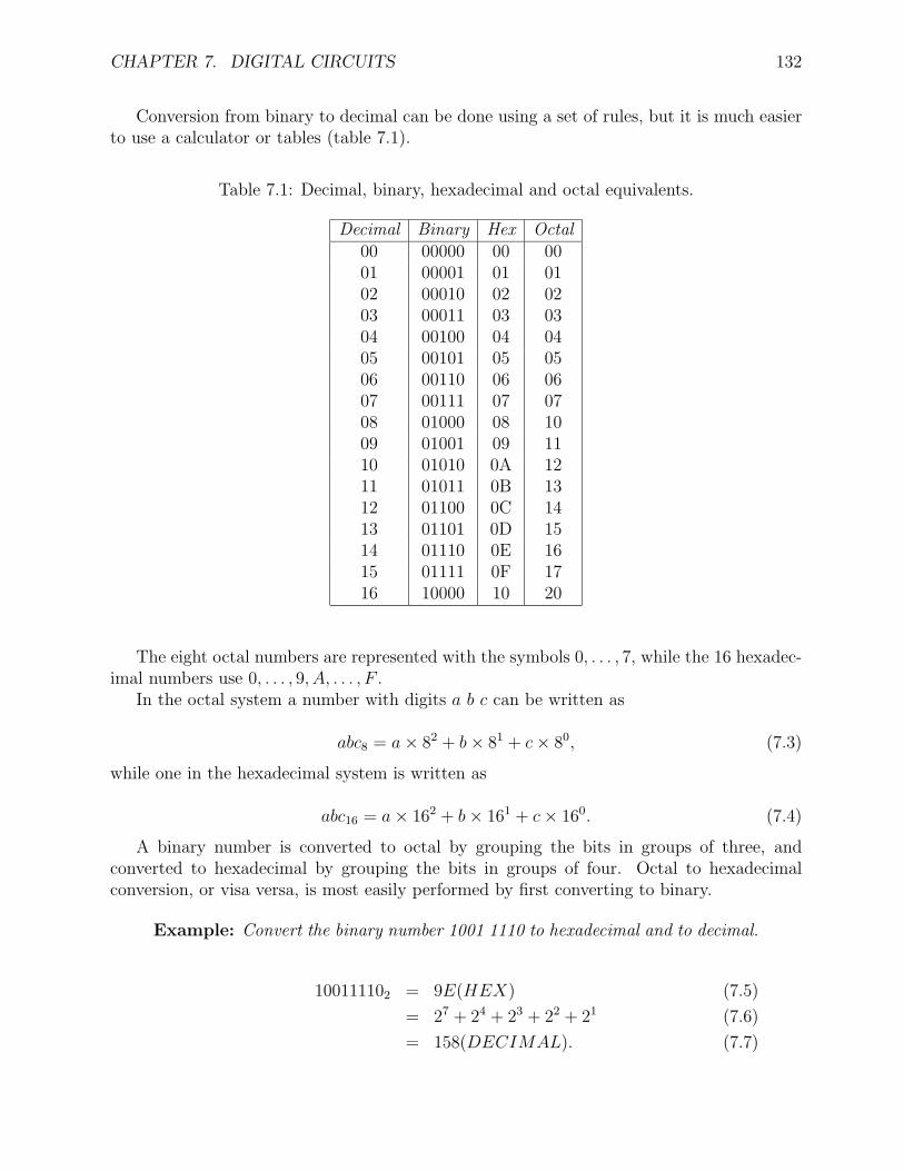
CHAPTER 7. DIGITAL CIRCUITS 132
Conversion from binary to decimal can be done using a set of rules, but it is much easierto use a calculator or tables (table 7.1).
Table 7.1: Decimal, binary, hexadecimal and octal equivalents.
Decimal Binary Hex Octal00 00000 00 0001 00001 01 0102 00010 02 0203 00011 03 0304 00100 04 0405 00101 05 0506 00110 06 0607 00111 07 0708 01000 08 1009 01001 09 1110 01010 0A 1211 01011 0B 1312 01100 0C 1413 01101 0D 1514 01110 0E 1615 01111 0F 1716 10000 10 20
The eight octal numbers are represented with the symbols 0, . . . , 7, while the 16 hexadec-imal numbers use 0, . . . , 9, A, . . . , F .
In the octal system a number with digits a b c can be written as
abc8 = a × 82 + b × 81 + c × 80, (7.3)
while one in the hexadecimal system is written as
abc16 = a × 162 + b × 161 + c × 160. (7.4)
A binary number is converted to octal by grouping the bits in groups of three, andconverted to hexadecimal by grouping the bits in groups of four. Octal to hexadecimalconversion, or visa versa, is most easily performed by first converting to binary.
Example: Convert the binary number 1001 1110 to hexadecimal and to decimal.
100111102 = 9E(HEX) (7.5)
= 27 + 24 + 23 + 22 + 21 (7.6)
= 158(DECIMAL). (7.7)
CHAPTER 7. DIGITAL CIRCUITS 133
Example: Convert the octal number 1758 to hexadecimal.
1758 = 0011111012 (7.8)
= 07D(HEX). (7.9)
Example: Convert the number 146 to binary by repeated subtraction of thelargest power of 2 contained in the remaining number.
14610 = 128 + 16 + 2 (7.10)
= 27 + 24 + 21 (7.11)
= 100100102. (7.12)
Example: Devise a method similar to that used in the previous problem andconvert 785 to hexadecimal by subtracting powers of 16.
78510 = 3 × 162 + 16 + 1 (7.13)
= 311(HEX). (7.14)
7.1.2 Number Representation
We define the following
word: a binary number consisting of an arbitrary number of bits.
nibble: a 4-bit word (one hexadecimal digit).
byte: an 8-bit word.
We often use the expressions 16-bit word (short word) or 32-bit word (long word) dependingon the type of computer being used. Most fast computers today actually employ a 64-bitword at the hardware level.
If a word has n bits it can represent 2n different numbers in the range 0 to 2n−1. Negativenumbers are usually represented by the so called 2’s complement notation. To obtain the2’s compliment of a number first take the complement (invert each bit) and then add 1. Allthe negative numbers will have a 1 in the MSB position, and the numbers will now rangefrom −2n−1 to 2n−1 − 1. The electronic advantages of the 2’s complement notation becomesevident when addition is performed. Convince yourself of this advantage.
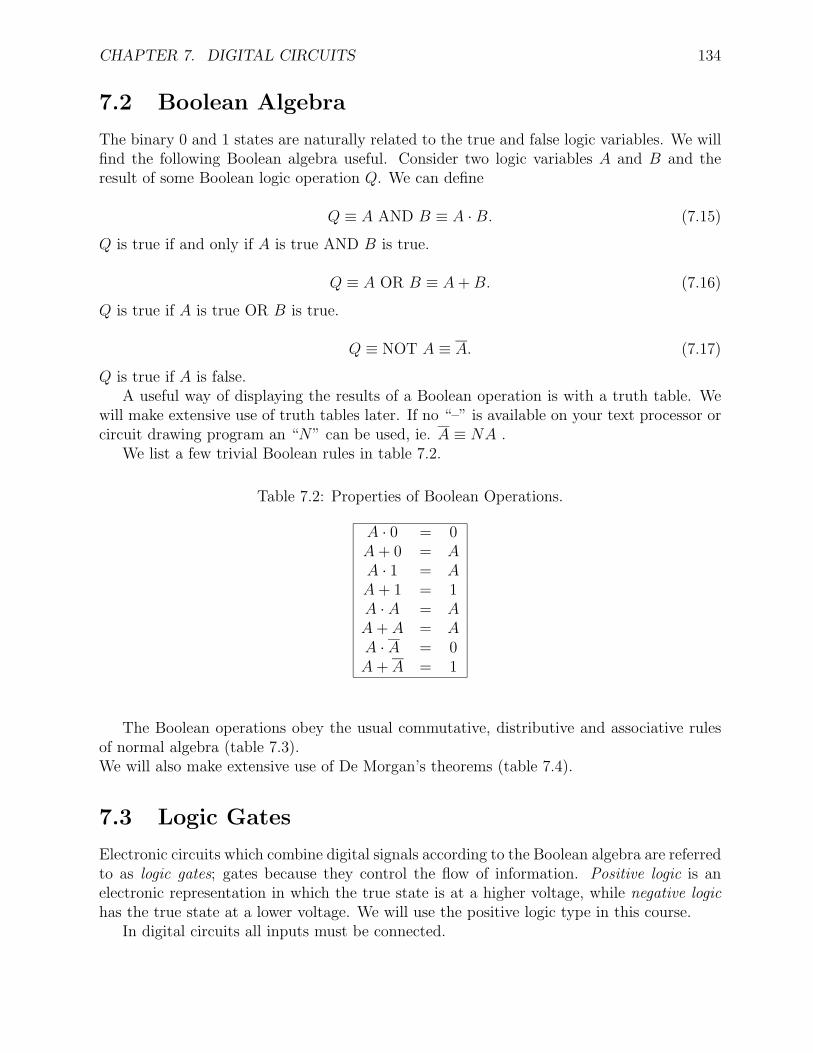
CHAPTER 7. DIGITAL CIRCUITS 134
7.2 Boolean Algebra
The binary 0 and 1 states are naturally related to the true and false logic variables. We willfind the following Boolean algebra useful. Consider two logic variables A and B and theresult of some Boolean logic operation Q. We can define
Q ≡ A AND B ≡ A · B. (7.15)
Q is true if and only if A is true AND B is true.
Q ≡ A OR B ≡ A + B. (7.16)
Q is true if A is true OR B is true.
Q ≡ NOT A ≡ A. (7.17)
Q is true if A is false.A useful way of displaying the results of a Boolean operation is with a truth table. We
will make extensive use of truth tables later. If no “–” is available on your text processor orcircuit drawing program an “N” can be used, ie. A ≡ NA .
We list a few trivial Boolean rules in table 7.2.
Table 7.2: Properties of Boolean Operations.
A · 0 = 0A + 0 = AA · 1 = AA + 1 = 1A · A = AA + A = AA · A = 0A + A = 1
The Boolean operations obey the usual commutative, distributive and associative rulesof normal algebra (table 7.3).We will also make extensive use of De Morgan’s theorems (table 7.4).
7.3 Logic Gates
Electronic circuits which combine digital signals according to the Boolean algebra are referredto as logic gates; gates because they control the flow of information. Positive logic is anelectronic representation in which the true state is at a higher voltage, while negative logichas the true state at a lower voltage. We will use the positive logic type in this course.
In digital circuits all inputs must be connected.
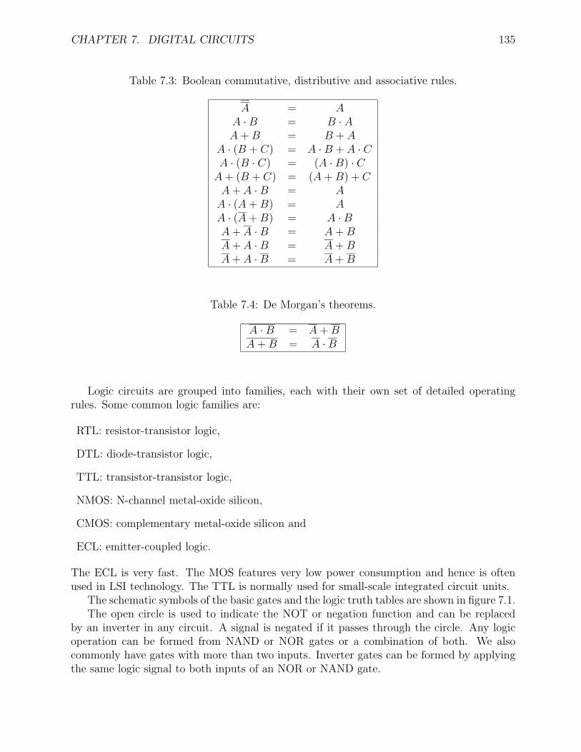
CHAPTER 7. DIGITAL CIRCUITS 135
Table 7.3: Boolean commutative, distributive and associative rules.
A = AA · B = B · AA + B = B + A
A · (B + C) = A · B + A · CA · (B · C) = (A · B) · C
A + (B + C) = (A + B) + CA + A · B = A
A · (A + B) = AA · (A + B) = A · BA + A · B = A + BA + A · B = A + BA + A · B = A + B
Table 7.4: De Morgan’s theorems.
A · B = A + BA + B = A · B
Logic circuits are grouped into families, each with their own set of detailed operatingrules. Some common logic families are:
RTL: resistor-transistor logic,
DTL: diode-transistor logic,
TTL: transistor-transistor logic,
NMOS: N-channel metal-oxide silicon,
CMOS: complementary metal-oxide silicon and
ECL: emitter-coupled logic.
The ECL is very fast. The MOS features very low power consumption and hence is oftenused in LSI technology. The TTL is normally used for small-scale integrated circuit units.
The schematic symbols of the basic gates and the logic truth tables are shown in figure 7.1.The open circle is used to indicate the NOT or negation function and can be replaced
by an inverter in any circuit. A signal is negated if it passes through the circle. Any logicoperation can be formed from NAND or NOR gates or a combination of both. We alsocommonly have gates with more than two inputs. Inverter gates can be formed by applyingthe same logic signal to both inputs of an NOR or NAND gate.
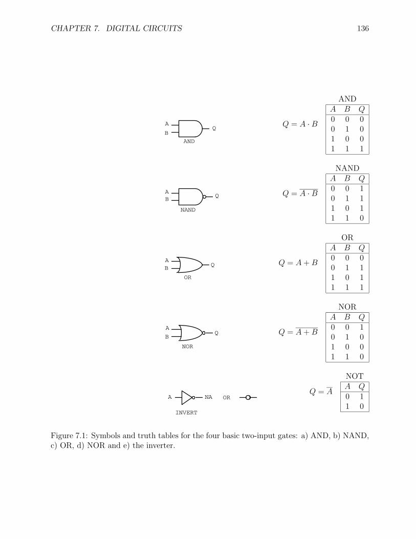
CHAPTER 7. DIGITAL CIRCUITS 136
Q = A · B
ANDA B Q0 0 00 1 01 0 01 1 1
Q = A · B
NANDA B Q0 0 10 1 11 0 11 1 0
Q = A + B
ORA B Q0 0 00 1 11 0 11 1 1
Q = A + B
NORA B Q0 0 10 1 01 0 01 1 0
Q = A
NOTA Q0 11 0
OR
INVERT
NOR
NAND
AND
OR
NA
Q
Q
Q
Q
A
B
A
BA
BA
B
A
Figure 7.1: Symbols and truth tables for the four basic two-input gates: a) AND, b) NAND,c) OR, d) NOR and e) the inverter.
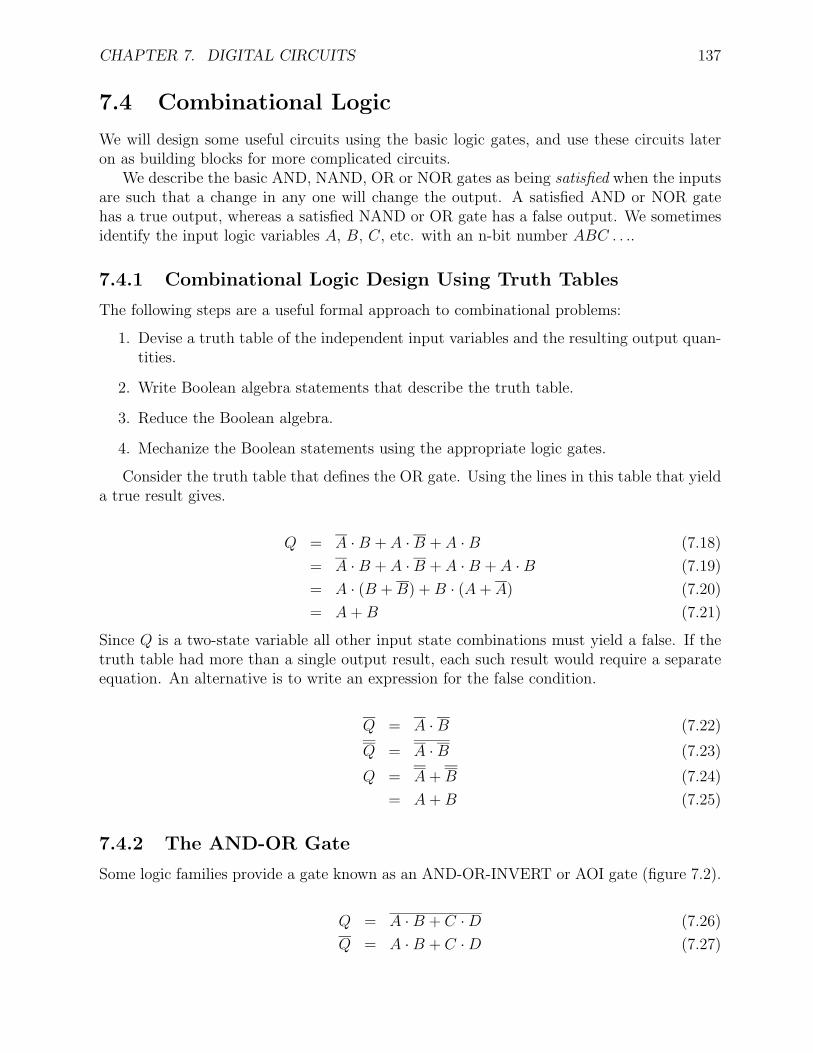
CHAPTER 7. DIGITAL CIRCUITS 137
7.4 Combinational Logic
We will design some useful circuits using the basic logic gates, and use these circuits lateron as building blocks for more complicated circuits.
We describe the basic AND, NAND, OR or NOR gates as being satisfied when the inputsare such that a change in any one will change the output. A satisfied AND or NOR gatehas a true output, whereas a satisfied NAND or OR gate has a false output. We sometimesidentify the input logic variables A, B, C, etc. with an n-bit number ABC . . ..
7.4.1 Combinational Logic Design Using Truth Tables
The following steps are a useful formal approach to combinational problems:
1. Devise a truth table of the independent input variables and the resulting output quan-tities.
2. Write Boolean algebra statements that describe the truth table.
3. Reduce the Boolean algebra.
4. Mechanize the Boolean statements using the appropriate logic gates.
Consider the truth table that defines the OR gate. Using the lines in this table that yielda true result gives.
Q = A · B + A · B + A · B (7.18)
= A · B + A · B + A · B + A · B (7.19)
= A · (B + B) + B · (A + A) (7.20)
= A + B (7.21)
Since Q is a two-state variable all other input state combinations must yield a false. If thetruth table had more than a single output result, each such result would require a separateequation. An alternative is to write an expression for the false condition.
Q = A · B (7.22)
Q = A · B (7.23)
Q = A + B (7.24)
= A + B (7.25)
7.4.2 The AND-OR Gate
Some logic families provide a gate known as an AND-OR-INVERT or AOI gate (figure 7.2).
Q = A · B + C · D (7.26)
Q = A · B + C · D (7.27)
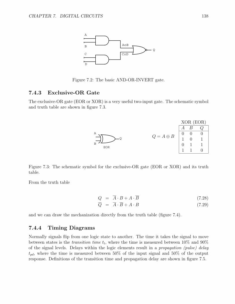
CHAPTER 7. DIGITAL CIRCUITS 138
CoD
AoB
Q
D
C
B
A
Figure 7.2: The basic AND-OR-INVERT gate.
7.4.3 Exclusive-OR Gate
The exclusive-OR gate (EOR or XOR) is a very useful two-input gate. The schematic symboland truth table are shown in figure 7.3.
Q = A ⊕ B
XOR (EOR)A B Q0 0 01 0 10 1 11 1 0
EOR
Q
B
A
Figure 7.3: The schematic symbol for the exclusive-OR gate (EOR or XOR) and its truthtable.
From the truth table
Q = A · B + A · B (7.28)
Q = A · B + A · B (7.29)
and we can draw the mechanization directly from the truth table (figure 7.4).
7.4.4 Timing Diagrams
Normally signals flip from one logic state to another. The time it takes the signal to movebetween states is the transition time tt, where the time is measured between 10% and 90%of the signal levels. Delays within the logic elements result in a propagation (pulse) delaytpd, where the time is measured between 50% of the input signal and 50% of the outputresponse. Definitions of the transition time and propagation delay are shown in figure 7.5.
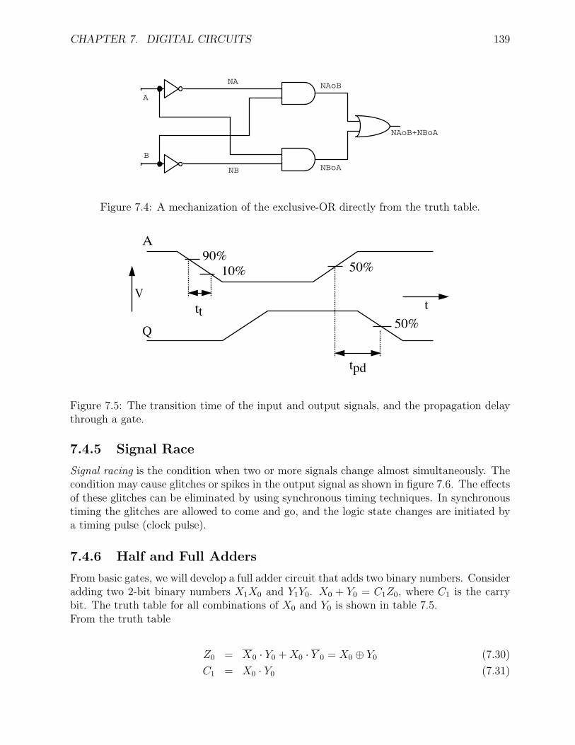
CHAPTER 7. DIGITAL CIRCUITS 139
NAoB+NBoA
NBoA
NAoB
NB
NA
B
A
Figure 7.4: A mechanization of the exclusive-OR directly from the truth table.
90%10%
50%
50%
tt
tpd
tV
A
Q
Figure 7.5: The transition time of the input and output signals, and the propagation delaythrough a gate.
7.4.5 Signal Race
Signal racing is the condition when two or more signals change almost simultaneously. Thecondition may cause glitches or spikes in the output signal as shown in figure 7.6. The effectsof these glitches can be eliminated by using synchronous timing techniques. In synchronoustiming the glitches are allowed to come and go, and the logic state changes are initiated bya timing pulse (clock pulse).
7.4.6 Half and Full Adders
From basic gates, we will develop a full adder circuit that adds two binary numbers. Consideradding two 2-bit binary numbers X1X0 and Y1Y0. X0 + Y0 = C1Z0, where C1 is the carrybit. The truth table for all combinations of X0 and Y0 is shown in table 7.5.From the truth table
Z0 = X0 · Y0 + X0 · Y 0 = X0 ⊕ Y0 (7.30)
C1 = X0 · Y0 (7.31)
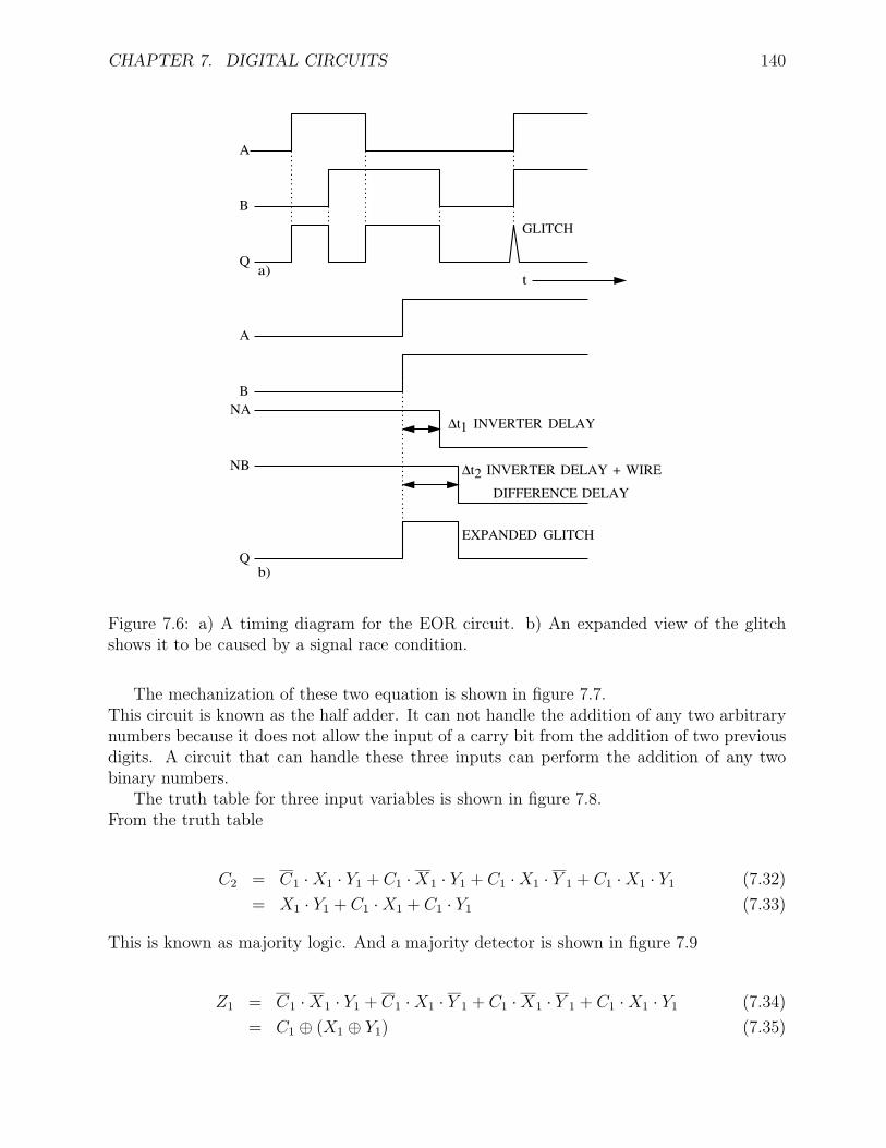
CHAPTER 7. DIGITAL CIRCUITS 140
A
B
Q
A
BNA
NB
Q
GLITCH
∆t1 INVERTER DELAY
∆t2 INVERTER DELAY + WIRE
DIFFERENCE DELAY
EXPANDED GLITCH
t
b)
a)
Figure 7.6: a) A timing diagram for the EOR circuit. b) An expanded view of the glitchshows it to be caused by a signal race condition.
The mechanization of these two equation is shown in figure 7.7.This circuit is known as the half adder. It can not handle the addition of any two arbitrarynumbers because it does not allow the input of a carry bit from the addition of two previousdigits. A circuit that can handle these three inputs can perform the addition of any twobinary numbers.
The truth table for three input variables is shown in figure 7.8.From the truth table
C2 = C1 · X1 · Y1 + C1 · X1 · Y1 + C1 · X1 · Y 1 + C1 · X1 · Y1 (7.32)
= X1 · Y1 + C1 · X1 + C1 · Y1 (7.33)
This is known as majority logic. And a majority detector is shown in figure 7.9
Z1 = C1 · X1 · Y1 + C1 · X1 · Y 1 + C1 · X1 · Y 1 + C1 · X1 · Y1 (7.34)
= C1 ⊕ (X1 ⊕ Y1) (7.35)
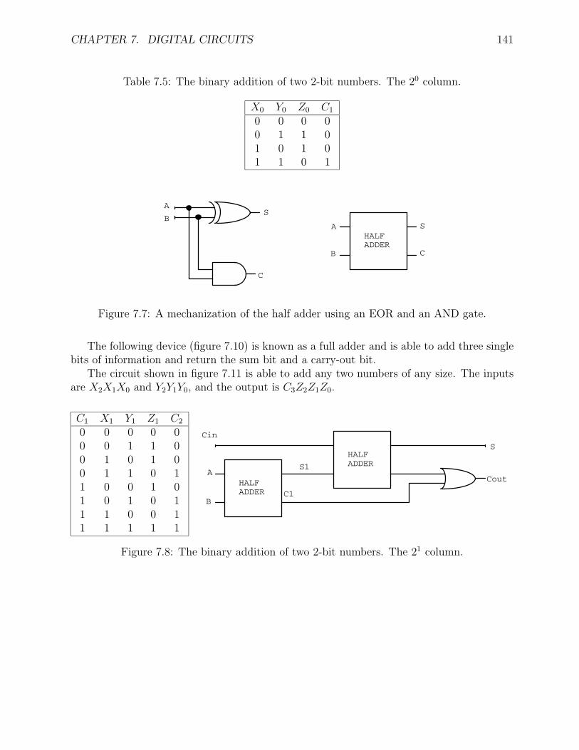
CHAPTER 7. DIGITAL CIRCUITS 141
Table 7.5: The binary addition of two 2-bit numbers. The 20 column.
X0 Y0 Z0 C1
0 0 0 00 1 1 01 0 1 01 1 0 1
S
CB
A
C
SB
A
HALFADDER
Figure 7.7: A mechanization of the half adder using an EOR and an AND gate.
The following device (figure 7.10) is known as a full adder and is able to add three singlebits of information and return the sum bit and a carry-out bit.
The circuit shown in figure 7.11 is able to add any two numbers of any size. The inputsare X2X1X0 and Y2Y1Y0, and the output is C3Z2Z1Z0.
C1 X1 Y1 Z1 C2
0 0 0 0 00 0 1 1 00 1 0 1 00 1 1 0 11 0 0 1 01 0 1 0 11 1 0 0 11 1 1 1 1
S
Cout
C1
S1
Cin
B
AHALFADDER
HALFADDER
Figure 7.8: The binary addition of two 2-bit numbers. The 21 column.
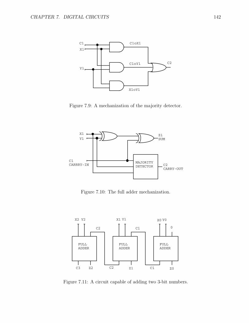
CHAPTER 7. DIGITAL CIRCUITS 142
C2C1oY1
X1oY1
C1oX1
Y1
X1
C1
Figure 7.9: A mechanization of the majority detector.
C1CARRRY-IN C2
CARRY-OUT
Z1SUMY1
X1
MAJORITYDETECTOR
Figure 7.10: The full adder mechanization.
C3 Z2 C2 Z1 C1 Z0
0
Y0X0
C1
Y1X1
C2
Y2X2
FULLADDER
FULLADDER
FULLADDER
Figure 7.11: A circuit capable of adding two 3-bit numbers.
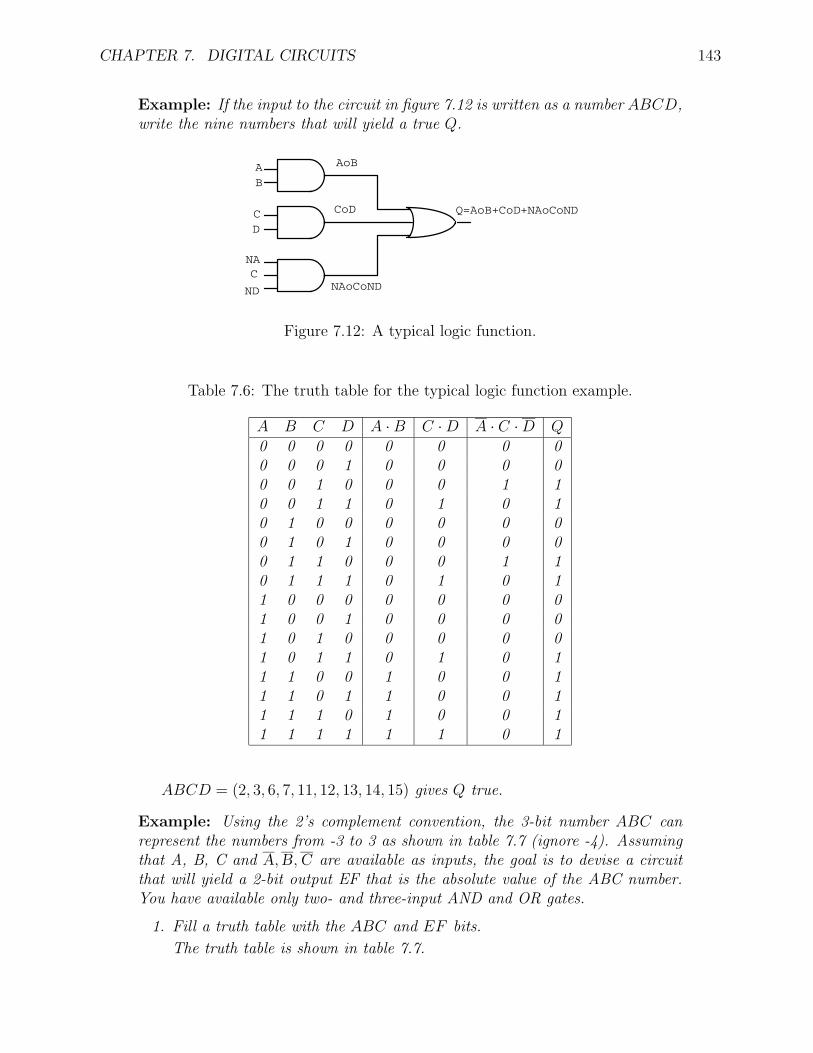
CHAPTER 7. DIGITAL CIRCUITS 143
Example: If the input to the circuit in figure 7.12 is written as a number ABCD,write the nine numbers that will yield a true Q.
NAoCoNDND
Q=AoB+CoD+NAoCoNDCoD
AoB
CNA
DC
BA
Figure 7.12: A typical logic function.
Table 7.6: The truth table for the typical logic function example.
A B C D A · B C · D A · C · D Q0 0 0 0 0 0 0 00 0 0 1 0 0 0 00 0 1 0 0 0 1 10 0 1 1 0 1 0 10 1 0 0 0 0 0 00 1 0 1 0 0 0 00 1 1 0 0 0 1 10 1 1 1 0 1 0 11 0 0 0 0 0 0 01 0 0 1 0 0 0 01 0 1 0 0 0 0 01 0 1 1 0 1 0 11 1 0 0 1 0 0 11 1 0 1 1 0 0 11 1 1 0 1 0 0 11 1 1 1 1 1 0 1
ABCD = (2, 3, 6, 7, 11, 12, 13, 14, 15) gives Q true.
Example: Using the 2’s complement convention, the 3-bit number ABC canrepresent the numbers from -3 to 3 as shown in table 7.7 (ignore -4). Assumingthat A, B, C and A, B, C are available as inputs, the goal is to devise a circuitthat will yield a 2-bit output EF that is the absolute value of the ABC number.You have available only two- and three-input AND and OR gates.
1. Fill a truth table with the ABC and EF bits.
The truth table is shown in table 7.7.
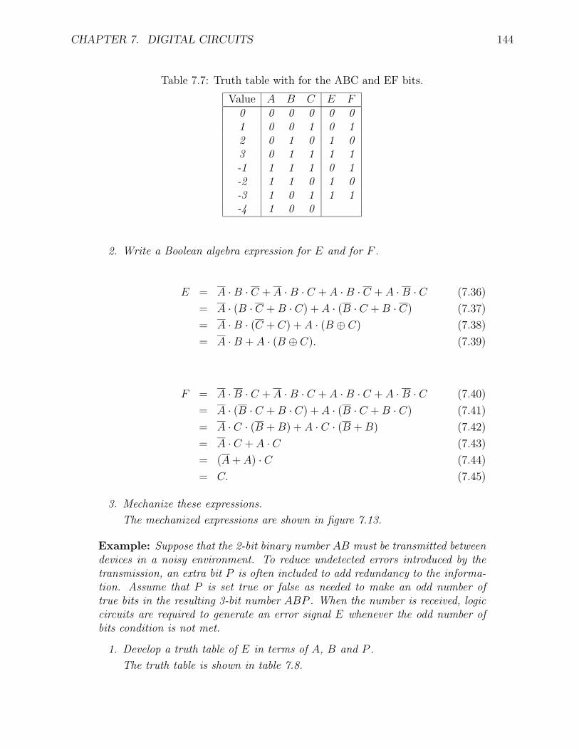
CHAPTER 7. DIGITAL CIRCUITS 144
Table 7.7: Truth table with for the ABC and EF bits.
Value A B C E F0 0 0 0 0 01 0 0 1 0 12 0 1 0 1 03 0 1 1 1 1-1 1 1 1 0 1-2 1 1 0 1 0-3 1 0 1 1 1-4 1 0 0
2. Write a Boolean algebra expression for E and for F .
E = A · B · C + A · B · C + A · B · C + A · B · C (7.36)
= A · (B · C + B · C) + A · (B · C + B · C) (7.37)
= A · B · (C + C) + A · (B ⊕ C) (7.38)
= A · B + A · (B ⊕ C). (7.39)
F = A · B · C + A · B · C + A · B · C + A · B · C (7.40)
= A · (B · C + B · C) + A · (B · C + B · C) (7.41)
= A · C · (B + B) + A · C · (B + B) (7.42)
= A · C + A · C (7.43)
= (A + A) · C (7.44)
= C. (7.45)
3. Mechanize these expressions.
The mechanized expressions are shown in figure 7.13.
Example: Suppose that the 2-bit binary number AB must be transmitted betweendevices in a noisy environment. To reduce undetected errors introduced by thetransmission, an extra bit P is often included to add redundancy to the informa-tion. Assume that P is set true or false as needed to make an odd number oftrue bits in the resulting 3-bit number ABP . When the number is received, logiccircuits are required to generate an error signal E whenever the odd number ofbits condition is not met.
1. Develop a truth table of E in terms of A, B and P .
The truth table is shown in table 7.8.
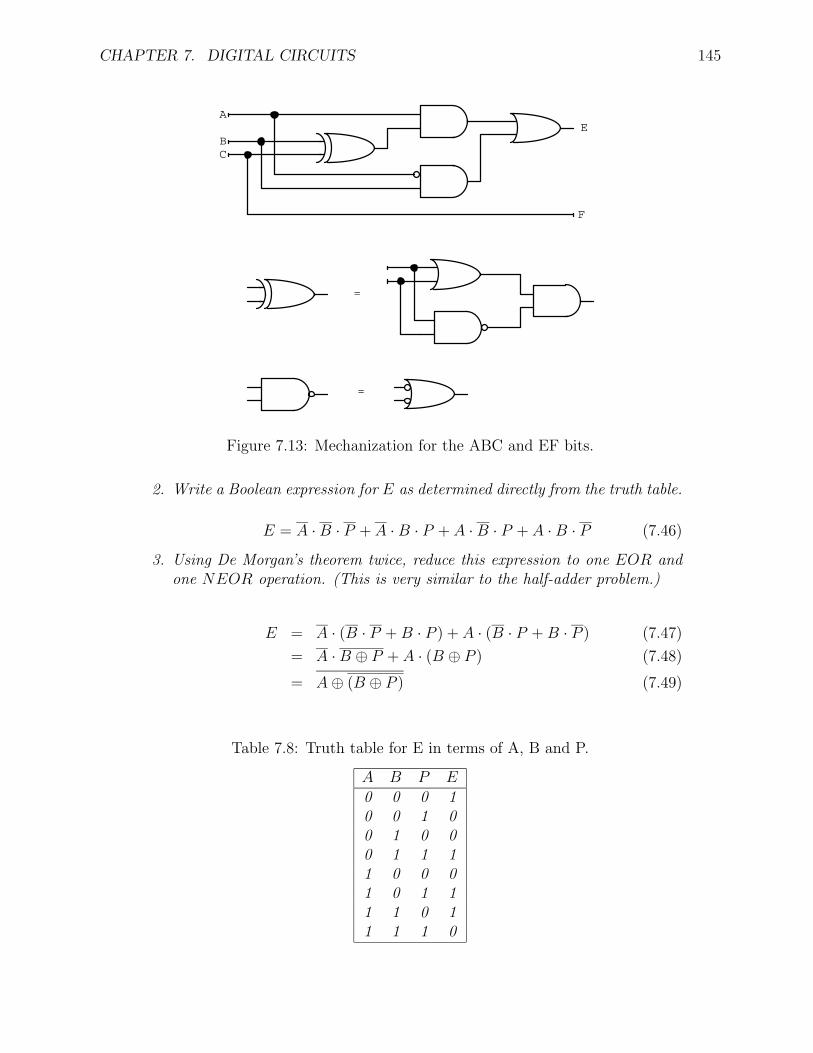
CHAPTER 7. DIGITAL CIRCUITS 145
F
=
=
AE
BC
Figure 7.13: Mechanization for the ABC and EF bits.
2. Write a Boolean expression for E as determined directly from the truth table.
E = A · B · P + A · B · P + A · B · P + A · B · P (7.46)
3. Using De Morgan’s theorem twice, reduce this expression to one EOR andone NEOR operation. (This is very similar to the half-adder problem.)
E = A · (B · P + B · P ) + A · (B · P + B · P ) (7.47)
= A · B ⊕ P + A · (B ⊕ P ) (7.48)
= A ⊕ (B ⊕ P ) (7.49)
Table 7.8: Truth table for E in terms of A, B and P.
A B P E0 0 0 10 0 1 00 1 0 00 1 1 11 0 0 01 0 1 11 1 0 11 1 1 0
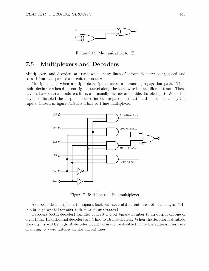
CHAPTER 7. DIGITAL CIRCUITS 146
BP
AE
Figure 7.14: Mechanization for E.
7.5 Multiplexers and Decoders
Multiplexers and decoders are used when many lines of information are being gated andpassed from one part of a circuit to another.
Multiplexing is when multiple data signals share a common propagation path. Timemultiplexing is when different signals travel along the same wire but at different times. Thesedevices have data and address lines, and usually include an enable/disable input. When thedevice is disabled the output is locked into some particular state and is not effected by theinputs. Shown in figure 7.15 is a 4-line to 1-line multiplexer.
A0oA1oS3
NA0oA1oS2
A0oNA1oS1
NA0oNA1oS0
A1
A0
S3
S2
S1
S0
Figure 7.15: 4-line to 1-line multiplexer.
A decoder de-multiplexes the signals back onto several different lines. Shown in figure 7.16is a binary-to-octal decoder (3-line to 8-line decoder).
Decoders (octal decoder) can also convert a 3-bit binary number to an output on one ofeight lines. Hexadecimal decoders are 4-line to 16-line devices. When the decoder is disabledthe outputs will be high. A decoder would normally be disabled while the address lines werechanging to avoid glitches on the output lines.
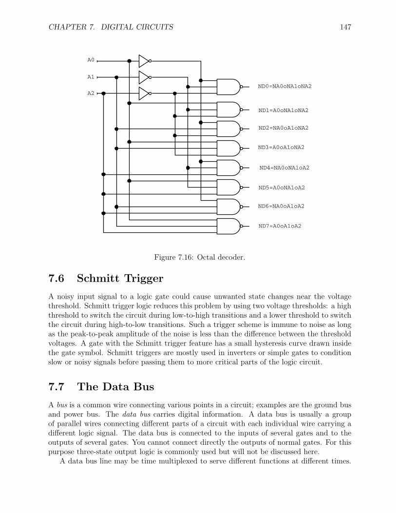
CHAPTER 7. DIGITAL CIRCUITS 147
ND7=A0oA1oA2
ND6=NA0oA1oA2
ND5=A0oNA1oA2
ND4=NA0oNA1oA2
ND3=A0oA1oNA2
ND2=NA0oA1oNA2
ND1=A0oNA1oNA2
ND0=NA0oNA1oNA2A2
A1
A0
Figure 7.16: Octal decoder.
7.6 Schmitt Trigger
A noisy input signal to a logic gate could cause unwanted state changes near the voltagethreshold. Schmitt trigger logic reduces this problem by using two voltage thresholds: a highthreshold to switch the circuit during low-to-high transitions and a lower threshold to switchthe circuit during high-to-low transitions. Such a trigger scheme is immune to noise as longas the peak-to-peak amplitude of the noise is less than the difference between the thresholdvoltages. A gate with the Schmitt trigger feature has a small hysteresis curve drawn insidethe gate symbol. Schmitt triggers are mostly used in inverters or simple gates to conditionslow or noisy signals before passing them to more critical parts of the logic circuit.
7.7 The Data Bus
A bus is a common wire connecting various points in a circuit; examples are the ground busand power bus. The data bus carries digital information. A data bus is usually a groupof parallel wires connecting different parts of a circuit with each individual wire carrying adifferent logic signal. The data bus is connected to the inputs of several gates and to theoutputs of several gates. You cannot connect directly the outputs of normal gates. For thispurpose three-state output logic is commonly used but will not be discussed here.
A data bus line may be time multiplexed to serve different functions at different times.
CHAPTER 7. DIGITAL CIRCUITS 148
At any time only one gate may drive information onto the bus line but several gates mayreceive it. In general, information may flow on the bus wires in both directions. This typeof bus is referred to as a bidirectional data bus.
7.8 Two-State Storage Elements
Analog voltage storage times are limited since the charge on a capacitor will eventually leakaway. The problem of discrete storage reduces to the need to store a large number of two-state variables. The four commonly used methods are: 1) magnetic domain orientation, 2)presence or absence of charge (not amount of charge) on a capacitor, 3) presence or absenceof an electrical connection and 4) the DC current path through the latches and flip-flops ofa digital circuit. We will discuss only the latter.
7.9 Latches and Un-Clocked Flip-Flops
It is possible using basic logic gates to build a circuit that remembers its present condition.It is also possible to build counting circuits. The basic counting unit is the flip-flop (FF).
7.9.1 Latches
All latches have two inputs: data and enable/disable. And typically Q and Q outputs. Aones-catching latch can be built as shown in figure 7.17.When the control input C is false, the output Q follows the input D, but when the con-trol input goes true, the output latches true as soon as D goes true and then stays thereindependent of further changes in D.
One of the most useful latches is known as the transparent latch or D-type latch. Thetransparent latch is like the ones-catching latch but the input D is frozen when the latch isdisabled. The operation of this latch is the same as that of the statically triggered D flip-flopdiscussed below.
7.9.2 RS and RS Flip-Flops
The RS flip-flop (RSFF) is the result of cross-connecting two NOR gates as shown in fig-ure 7.18. The RS inputs are referred to as active ones.The ideal flip-flop has only two rest states, set and reset, defined by QQ = 10 and QQ = 01,respectively.
A very similar flip-flop can be constructed using two NAND gates as shown in figure 7.19.The RS inputs are now active zeros.
These FFs are often referred to as the set/reset type and are un-clocked.
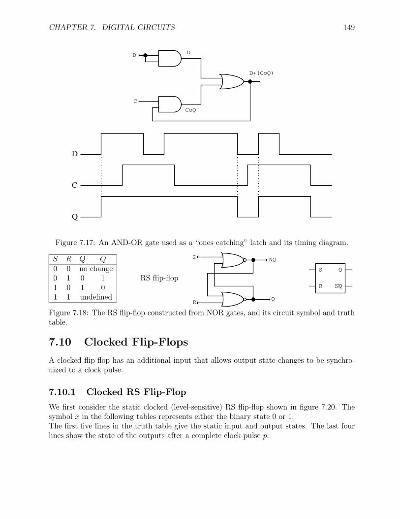
CHAPTER 7. DIGITAL CIRCUITS 149
D+(CoQ)
CoQ
D
C
D
D
C
Q
Figure 7.17: An AND-OR gate used as a “ones catching” latch and its timing diagram.
S R Q Q0 0 no change0 1 0 11 0 1 01 1 undefined
RS flip-flop
Q
NQ
R
S
S
R
Q
NQ
Figure 7.18: The RS flip-flop constructed from NOR gates, and its circuit symbol and truthtable.
7.10 Clocked Flip-Flops
A clocked flip-flop has an additional input that allows output state changes to be synchro-nized to a clock pulse.
7.10.1 Clocked RS Flip-Flop
We first consider the static clocked (level-sensitive) RS flip-flop shown in figure 7.20. Thesymbol x in the following tables represents either the binary state 0 or 1.The first five lines in the truth table give the static input and output states. The last fourlines show the state of the outputs after a complete clock pulse p.
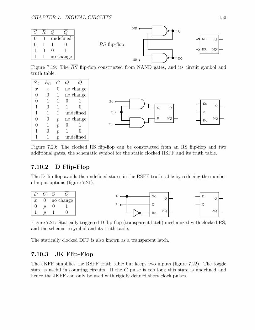
CHAPTER 7. DIGITAL CIRCUITS 150
S R Q Q0 0 undefined0 1 1 01 0 0 11 1 no change
RS flip-flop
NQ
Q
NR
NS
NS
NR
Q
NQ
Figure 7.19: The RS flip-flop constructed from NAND gates, and its circuit symbol andtruth table.
SC RC C Q Qx x 0 no change0 0 1 no change0 1 1 0 11 0 1 1 01 1 1 undefined0 0 p no change0 1 p 0 11 0 p 1 01 1 p undefined
Rc
C
Sc
S
R
Q
NQ
Sc
Rc
C
Q
NQ
Figure 7.20: The clocked RS flip-flop can be constructed from an RS flip-flop and twoadditional gates, the schematic symbol for the static clocked RSFF and its truth table.
7.10.2 D Flip-Flop
The D flip-flop avoids the undefined states in the RSFF truth table by reducing the numberof input options (figure 7.21).
D C Q Qx 0 no change0 p 0 11 p 1 0
C
D Sc
Rc
C
Q
NQ
D
C
Q
NQ
Figure 7.21: Statically triggered D flip-flop (transparent latch) mechanized with clocked RS,and the schematic symbol and its truth table.
The statically clocked DFF is also known as a transparent latch.
7.10.3 JK Flip-Flop
The JKFF simplifies the RSFF truth table but keeps two inputs (figure 7.22). The togglestate is useful in counting circuits. If the C pulse is too long this state is undefined andhence the JKFF can only be used with rigidly defined short clock pulses.
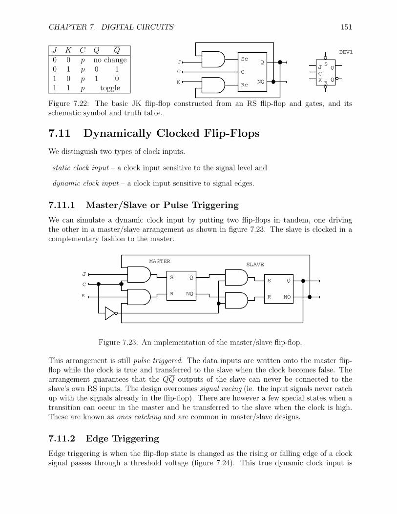
CHAPTER 7. DIGITAL CIRCUITS 151
J K C Q Q0 0 p no change0 1 p 0 11 0 p 1 01 1 p toggle
K
C
J Sc
Rc
C
Q
NQ
JCK
S
R
Q
Q
DEV1
Figure 7.22: The basic JK flip-flop constructed from an RS flip-flop and gates, and itsschematic symbol and truth table.
7.11 Dynamically Clocked Flip-Flops
We distinguish two types of clock inputs.
static clock input – a clock input sensitive to the signal level and
dynamic clock input – a clock input sensitive to signal edges.
7.11.1 Master/Slave or Pulse Triggering
We can simulate a dynamic clock input by putting two flip-flops in tandem, one drivingthe other in a master/slave arrangement as shown in figure 7.23. The slave is clocked in acomplementary fashion to the master.
SLAVEMASTER
K
C
JS
R
Q
NQ
S
R
Q
NQ
Figure 7.23: An implementation of the master/slave flip-flop.
This arrangement is still pulse triggered. The data inputs are written onto the master flip-flop while the clock is true and transferred to the slave when the clock becomes false. Thearrangement guarantees that the QQ outputs of the slave can never be connected to theslave’s own RS inputs. The design overcomes signal racing (ie. the input signals never catchup with the signals already in the flip-flop). There are however a few special states when atransition can occur in the master and be transferred to the slave when the clock is high.These are known as ones catching and are common in master/slave designs.
7.11.2 Edge Triggering
Edge triggering is when the flip-flop state is changed as the rising or falling edge of a clocksignal passes through a threshold voltage (figure 7.24). This true dynamic clock input is
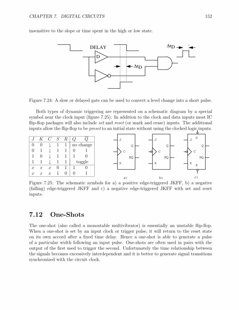
CHAPTER 7. DIGITAL CIRCUITS 152
insensitive to the slope or time spent in the high or low state.
DELAY
D
∆tD
∆tD
Figure 7.24: A slow or delayed gate can be used to convert a level change into a short pulse.
Both types of dynamic triggering are represented on a schematic diagram by a specialsymbol near the clock input (figure 7.25). In addition to the clock and data inputs most ICflip-flop packages will also include set and reset (or mark and erase) inputs. The additionalinputs allow the flip-flop to be preset to an initial state without using the clocked logic inputs.
J K C S R Q Q0 0 ↓ 1 1 no change0 1 ↓ 1 1 0 11 0 ↓ 1 1 1 01 1 ↓ 1 1 togglex x x 0 1 1 0x x x 1 0 0 1
c)b)a)
J J J
K K K
Q Q Q
NQ NQ NQ
C C C
S
R
Figure 7.25: The schematic symbols for a) a positive edge-triggered JKFF, b) a negative(falling) edge-triggered JKFF and c) a negative edge-triggered JKFF with set and resetinputs.
7.12 One-Shots
The one-shot (also called a monostable multivibrator) is essentially an unstable flip-flop.When a one-shot is set by an input clock or trigger pulse, it will return to the reset stateon its own accord after a fixed time delay. Hence a one-shot is able to generate a pulseof a particular width following an input pulse. One-shots are often used in pairs with theoutput of the first used to trigger the second. Unfortunately the time relationship betweenthe signals becomes excessively interdependent and it is better to generate signal transitionssynchronized with the circuit clock.
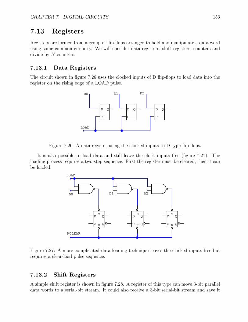
CHAPTER 7. DIGITAL CIRCUITS 153
7.13 Registers
Registers are formed from a group of flip-flops arranged to hold and manipulate a data wordusing some common circuitry. We will consider data registers, shift registers, counters anddivide-by-N counters.
7.13.1 Data Registers
The circuit shown in figure 7.26 uses the clocked inputs of D flip-flops to load data into theregister on the rising edge of a LOAD pulse.
D2D1D0
LOAD
D
C
Q D
C
Q D
C
Q
Figure 7.26: A data register using the clocked inputs to D-type flip-flops.
It is also possible to load data and still leave the clock inputs free (figure 7.27). Theloading process requires a two-step sequence. First the register must be cleared, then it canbe loaded.
NCLEAR
D2D1D0
LOAD
D
C
S
R
Q
Q
D
C
S
R
Q
Q
D
C
S
R
Q
Q
Figure 7.27: A more complicated data-loading technique leaves the clocked inputs free butrequires a clear-load pulse sequence.
7.13.2 Shift Registers
A simple shift register is shown in figure 7.28. A register of this type can move 3-bit paralleldata words to a serial-bit stream. It could also receive a 3-bit serial-bit stream and save it
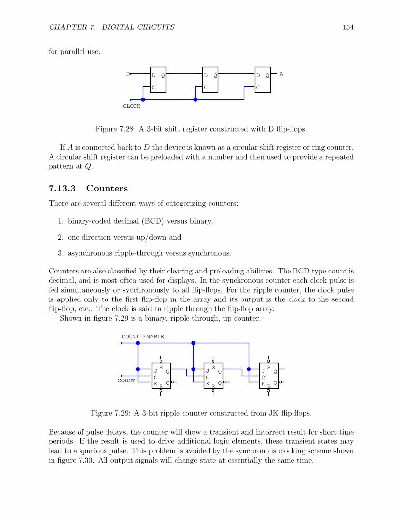
CHAPTER 7. DIGITAL CIRCUITS 154
for parallel use.
AD
CLOCK
D
C
Q D
C
Q D
C
Q
Figure 7.28: A 3-bit shift register constructed with D flip-flops.
If A is connected back to D the device is known as a circular shift register or ring counter.A circular shift register can be preloaded with a number and then used to provide a repeatedpattern at Q.
7.13.3 Counters
There are several different ways of categorizing counters:
1. binary-coded decimal (BCD) versus binary,
2. one direction versus up/down and
3. asynchronous ripple-through versus synchronous.
Counters are also classified by their clearing and preloading abilities. The BCD type count isdecimal, and is most often used for displays. In the synchronous counter each clock pulse isfed simultaneously or synchronously to all flip-flops. For the ripple counter, the clock pulseis applied only to the first flip-flop in the array and its output is the clock to the secondflip-flop, etc.. The clock is said to ripple through the flip-flop array.
Shown in figure 7.29 is a binary, ripple-through, up counter.
COUNT
COUNT ENABLE
JCK
S
R
Q
Q
JCK
S
R
Q
Q
JCK
S
R
Q
Q
Figure 7.29: A 3-bit ripple counter constructed from JK flip-flops.
Because of pulse delays, the counter will show a transient and incorrect result for short timeperiods. If the result is used to drive additional logic elements, these transient states maylead to a spurious pulse. This problem is avoided by the synchronous clocking scheme shownin figure 7.30. All output signals will change state at essentially the same time.
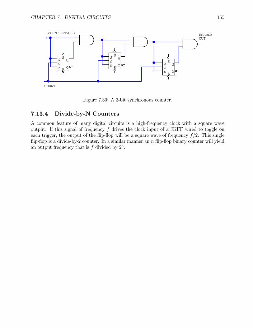
CHAPTER 7. DIGITAL CIRCUITS 155
ENABLEOUT
COUNT
COUNT ENABLE
JCK
S
R
Q
Q
JCK
S
R
Q
Q JCK
S
R
Q
Q
Figure 7.30: A 3-bit synchronous counter.
7.13.4 Divide-by-N Counters
A common feature of many digital circuits is a high-frequency clock with a square waveoutput. If this signal of frequency f drives the clock input of a JKFF wired to toggle oneach trigger, the output of the flip-flop will be a square wave of frequency f/2. This singleflip-flop is a divide-by-2 counter. In a similar manner an n flip-flop binary counter will yieldan output frequency that is f divided by 2n.
CHAPTER 7. DIGITAL CIRCUITS 156
7.14 Problems
1. Using only two-input NOR gates, show how AND, OR and NAND gates can be made.
2. The binary addition of two 2-bit numbers (with carry bits) looks like the following:
C2 C1
X1 X0
+ Y1 Y0
Z2 Z1 Z0
(a) Write a truth table expressing the outputs C2 and Z1 as a function of C1, X1 andY1.
(b) Write an algebraic statement in Boolean algebra describing this truth table.
(c) Implement this statement using standard (AND, OR, EX-OR and inverter gates).
3. If the 3-bit binary number ABC represents the digits 0 to 7:
(a) Make a truth table for A, B, C and Q, where Q is true only when an odd numberof bits are true in the number.
(b) Write a statement in Boolean algebra for Q.
(c) Convert this equation to one that can be mechanized using only two XOR gates.Draw the resulting circuit.
4. You need to provide a logic signal to control an experiment. The experiment is con-trolled by the four signals A,B,C and D, which make up the data word ABCD. Thecontrol line Q should be set high only if this data word takes on the values 1, 3, 5, 7,11 or 13.
(a) Write a truth table for this function.
(b) Using boolean algebra, write an expression indicating when Q is true. Yourstatement should include one logical statement for each of the six true conditions,each separated by the OR function. Therefore this statement should utilize anumber of AND/NAND functions, and five OR statements.
(c) Simplify this statement so that it can be implemented using two two-input ANDgates, one OR gate, one exclusive OR gate and one logical inverter. The expressionhas the form Q = ( ) · ( ) + ( ) · [( ) ⊕ ( )], where ( ) stands for any of the fourinput signals or their logical inverses.
(d) Implement this simplified function using logic gates.
Chapter 8
Data Acquisition and Process Control
The purpose of most electronic systems is to measure or control some physical quantity.The system will need to acquire data from the environment, process this data and record it.Acting as a control system it will also have to interact with the environment.
The flow of information in a typical data acquisition system (DAQ) can be described asfollows.
1. The input transducers measure some property of the environment.
2. The output from the transducers is conditioned (amplified, filtered, etc.).
3. The conditioned analog signal is digitized using an analog-to-digital converter (ADC).
4. The digital information is acquired, processed and recorded by the computer.
5. The computer may then modify the environment by outputting control signals.
6. The digital control signals are converted to analog signals using a digital-to-analogconverter (DAC).
7. The analog signals are conditioned (eg. amplified and filtered) appropriately for anoutput transducer.
8. The output transducer interacts with the environment.
8.1 Transducers
Electrical systems are only able to respond to voltage and current signals in the electricaldomain: amplitude, frequency, phase and time constant. An input transducer is necessaryto convert a signal from its domain of origin (non-electrical) into the electrical domain.
A transducer may generate an electrical signal by varying one of the following: voltage,current, resistance, capacitance, self-inductance, mutual-inductance, VPN , VZ , hfe or gm Themost fundamental transducers respond to temperature, electromagnetic radiation intensity,force, displacement or chemical concentration. If coupled to the time domain these devicescan be used to measure any physical or chemical quantity. Examples of input transducers
157
CHAPTER 8. DATA ACQUISITION AND PROCESS CONTROL 158
are: a radio antenna, a photo-diode, a phototube, a piezoelectric crystal, a thermocouple, aHall effect device, a mechanical switch, a strain gauge, an ionization chamber, etc..
The output transducer transfers signals out of the electrical domain and into the do-main that can be perceived by one of the five human senses. A substantial amount ofpower is usually required to transfer information out of the electrical domain. Examplesof output transducers are the motor, cathode-ray tube, loudspeaker, light-emitting diode,radio-frequency transmitter, etc.
8.2 Signal Conditioning Circuits
Signal conditioning occurs in the interface between the transducers and the electrical circuit.A low-level signal amplifier and a low-pass filter are common signal conditioners after theinput transducer. The output signal is usually conditioned by a low-pass filter and sometype of power amplifier.
8.2.1 De-bouncing the Mechanical Switch
The pushbutton or toggle switch is a simple form of data entry into a digital system. However,a problem occurs since the normal human reaction time is about 10−1 s and digital electronicsresponds to times of the order of 10−8 s. Thus any unnoticed mechanical contact bounce ofa few milliseconds will be seen as several distinct switch closures by a digital system. Wemay de-bounce the mechanical switch by using an RC circuit and Schmitt trigger logic ora flip-flop latch. The latter design requires a break-before-make action, which means thatduring the throw there is a time when the common is connected to neither terminal.
8.2.2 Op Amps for Gain, Offset and Function Modification
An operational amplifier can be used to provide the following signal conditioning:
1. increase the amplitude of the signal,
2. filter the signal,
3. decrease the signal output impedance or
4. provide a variable gain and offset control.
The latter is most useful for calibrating a transducer’s output signal.The dynamic range of a signal from an input transducer may be too large to process
through the DAQ system (eg. the ADC is often the limiting factor). One can use a linearamplifier and choose to overflow or reduce the overall gain. The latter approach will causea loss in precision. Another approach is to use a nonlinear amplifier, such as one with alogarithmic gain, Vout = log(Vin).
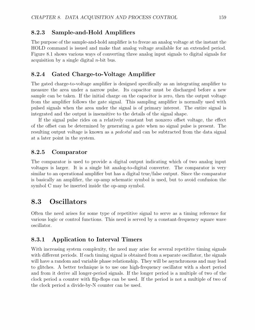
CHAPTER 8. DATA ACQUISITION AND PROCESS CONTROL 159
8.2.3 Sample-and-Hold Amplifiers
The purpose of the sample-and-hold amplifier is to freeze an analog voltage at the instant theHOLD command is issued and make that analog voltage available for an extended period.Figure 8.1 shows various ways of converting three analog input signals to digital signals foracquisition by a single digital n-bit bus.
8.2.4 Gated Charge-to-Voltage Amplifier
The gated charge-to-voltage amplifier is designed specifically as an integrating amplifier tomeasure the area under a narrow pulse. Its capacitor must be discharged before a newsample can be taken. If the initial charge on the capacitor is zero, then the output voltagefrom the amplifier follows the gate signal. This sampling amplifier is normally used withpulsed signals when the area under the signal is of primary interest. The entire signal isintegrated and the output is insensitive to the details of the signal shape.
If the signal pulse rides on a relatively constant but nonzero offset voltage, the effectof the offset can be determined by generating a gate when no signal pulse is present. Theresulting output voltage is known as a pedestal and can be subtracted from the data signalat a later point in the system.
8.2.5 Comparator
The comparator is used to provide a digital output indicating which of two analog inputvoltages is larger. It is a single bit analog-to-digital converter. The comparator is verysimilar to an operational amplifier but has a digital true/false output. Since the comparatoris basically an amplifier, the op-amp schematic symbol is used, but to avoid confusion thesymbol C may be inserted inside the op-amp symbol.
8.3 Oscillators
Often the need arises for some type of repetitive signal to serve as a timing reference forvarious logic or control functions. This need is served by a constant-frequency square waveoscillator.
8.3.1 Application to Interval Timers
With increasing system complexity, the need may arise for several repetitive timing signalswith different periods. If each timing signal is obtained from a separate oscillator, the signalswill have a random and variable phase relationship. They will be asynchronous and may leadto glitches. A better technique is to use one high-frequency oscillator with a short periodand from it derive all longer-period signals. If the longer period is a multiple of two of theclock period a counter with flip-flops can be used. If the period is not a multiple of two ofthe clock period a divide-by-N counter can be used.
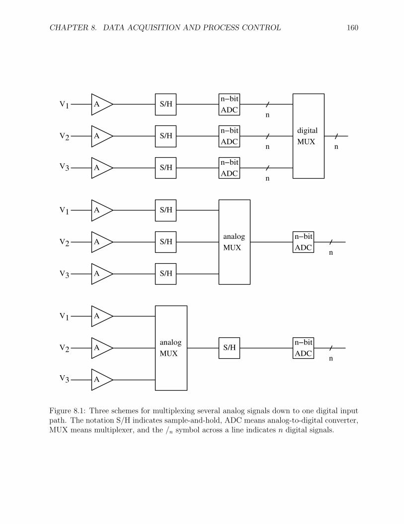
CHAPTER 8. DATA ACQUISITION AND PROCESS CONTROL 160
A
A
A
A
A
A
A
A
A
S/H
S/H
S/H
S/H
S/H
S/H
S/Hn−bit
ADC
n−bit
ADC
n−bit
ADC
n−bit
ADC
n−bit
ADC
analog
MUX
analog
MUX
digital
MUX
n
n
n
n
n
n
V1
V1
V1
V2
V2
V2
V3
V3
V3
Figure 8.1: Three schemes for multiplexing several analog signals down to one digital inputpath. The notation S/H indicates sample-and-hold, ADC means analog-to-digital converter,MUX means multiplexer, and the /n symbol across a line indicates n digital signals.
CHAPTER 8. DATA ACQUISITION AND PROCESS CONTROL 161
8.4 Digital-to-Analog Conversion
The process of converting a number held in a digital register to an analog voltage or currentis accomplished with a digital-to-analog converter (DAC). The DAC is a useful interfacebetween a computer and an output transducer.
8.4.1 Current Summing and IC Devices
DACs are normally switched current devices designed to drive the current-summing junctionof an operational amplifier. Figure 8.2 shows a simple 4-bit DAC.
VrefIm = ---- 2R
Im/8Im/4Im/2Im
16R8R4R2R
MSB DCBA
I
R
Iref
Vref
Vout
Figure 8.2: The current DAC uses the summing input to an op-amp to yield a voltage output.LSB and MSB refer to the least and most significant bits of a binary number.
Each current is proportional to the value of a bit position in a binary number.The design requires a number of different precisely defined resistor values. We can im-
prove the circuit by replacing it with a circuit that requires fewer distinct resistor values.
8.4.2 DAC Limitations
The output of a DAC can only assume discrete values. The relationship between the inputbinary number and the analog output of a perfect DAC is shown in figure 8.3.Common DAC limitations are an anomalous step size between adjacent binary numbers,non-monotonic behaviour, or a zero output.
8.5 Analog-to-Digital Conversion
The analog-to-digital converter (ADC) is used to convert an analog voltage to a digitalnumber (figure 8.4).
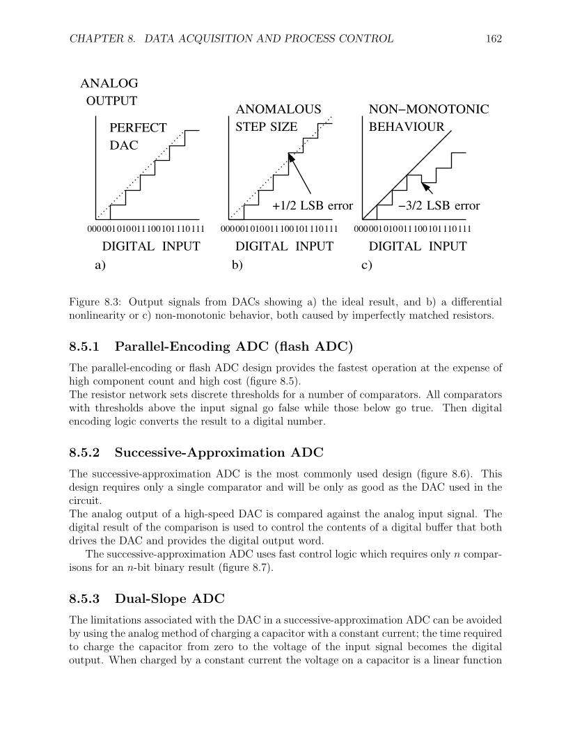
CHAPTER 8. DATA ACQUISITION AND PROCESS CONTROL 162
000001010011100101110111 000001010011100101110111 000001010011100101110111
DIGITAL INPUT DIGITAL INPUT DIGITAL INPUT
a) b) c)
ANALOGOUTPUT
PERFECTDAC
ANOMALOUSSTEP SIZE
NON−MONOTONICBEHAVIOUR
+1/2 LSB error −3/2 LSB error
Figure 8.3: Output signals from DACs showing a) the ideal result, and b) a differentialnonlinearity or c) non-monotonic behavior, both caused by imperfectly matched resistors.
8.5.1 Parallel-Encoding ADC (flash ADC)
The parallel-encoding or flash ADC design provides the fastest operation at the expense ofhigh component count and high cost (figure 8.5).The resistor network sets discrete thresholds for a number of comparators. All comparatorswith thresholds above the input signal go false while those below go true. Then digitalencoding logic converts the result to a digital number.
8.5.2 Successive-Approximation ADC
The successive-approximation ADC is the most commonly used design (figure 8.6). Thisdesign requires only a single comparator and will be only as good as the DAC used in thecircuit.The analog output of a high-speed DAC is compared against the analog input signal. Thedigital result of the comparison is used to control the contents of a digital buffer that bothdrives the DAC and provides the digital output word.
The successive-approximation ADC uses fast control logic which requires only n compar-isons for an n-bit binary result (figure 8.7).
8.5.3 Dual-Slope ADC
The limitations associated with the DAC in a successive-approximation ADC can be avoidedby using the analog method of charging a capacitor with a constant current; the time requiredto charge the capacitor from zero to the voltage of the input signal becomes the digitaloutput. When charged by a constant current the voltage on a capacitor is a linear function
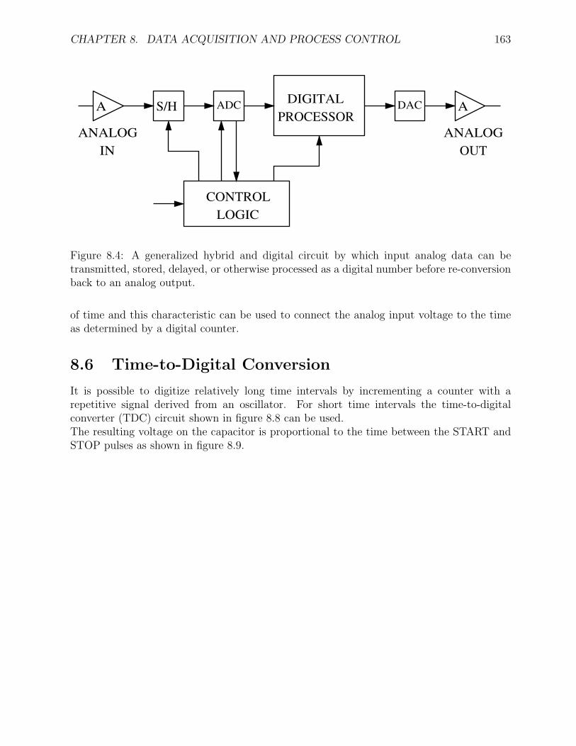
CHAPTER 8. DATA ACQUISITION AND PROCESS CONTROL 163
A S/H DAC AADC DIGITALPROCESSOR
CONTROLLOGIC
ANALOGIN
ANALOGOUT
Figure 8.4: A generalized hybrid and digital circuit by which input analog data can betransmitted, stored, delayed, or otherwise processed as a digital number before re-conversionback to an analog output.
of time and this characteristic can be used to connect the analog input voltage to the timeas determined by a digital counter.
8.6 Time-to-Digital Conversion
It is possible to digitize relatively long time intervals by incrementing a counter with arepetitive signal derived from an oscillator. For short time intervals the time-to-digitalconverter (TDC) circuit shown in figure 8.8 can be used.The resulting voltage on the capacitor is proportional to the time between the START andSTOP pulses as shown in figure 8.9.
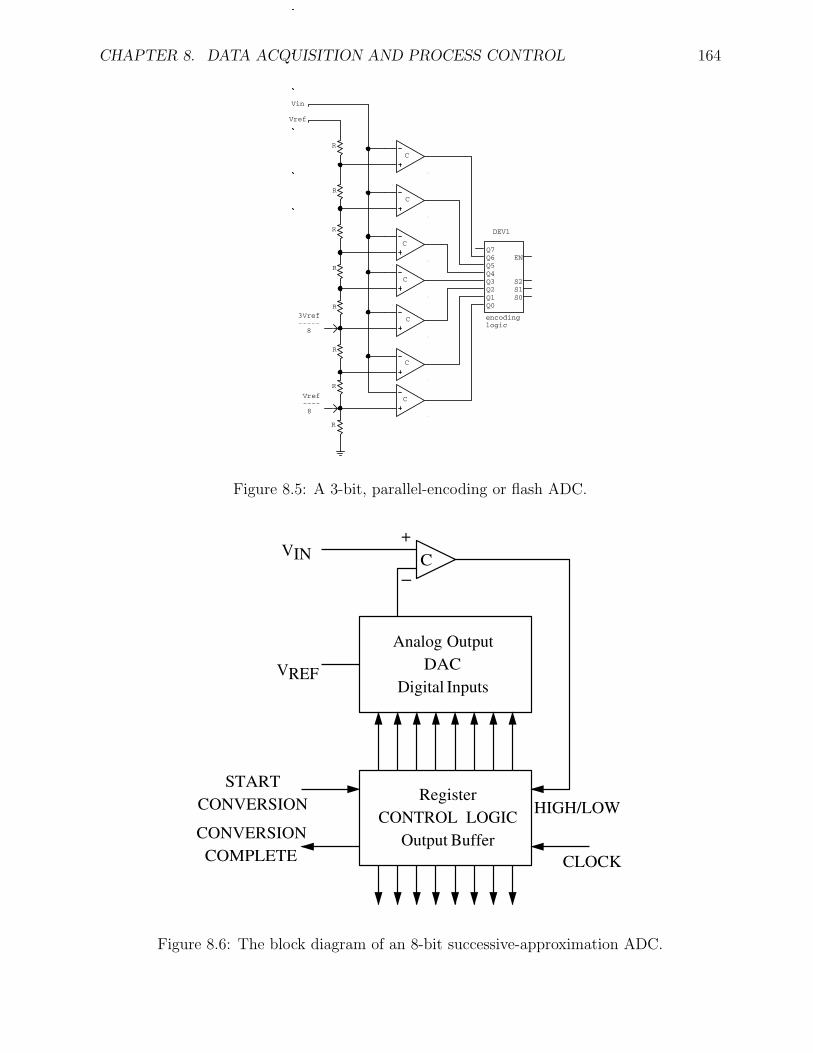
CHAPTER 8. DATA ACQUISITION AND PROCESS CONTROL 164
Vref---- 8
3Vref----- 8
C
C
C
C
C
C
C
encodinglogic
R
R
R
R
R
R
R
R
Vref
Vin
Q7Q6Q5Q4Q3Q2Q1Q0
S0S1S2
EN
DEV1
Figure 8.5: A 3-bit, parallel-encoding or flash ADC.
Analog OutputDAC
Digital Inputs
RegisterCONTROL LOGIC
Output Buffer
CVIN
VREF
+
−
HIGH/LOW
CLOCK
STARTCONVERSION
CONVERSIONCOMPLETE
Figure 8.6: The block diagram of an 8-bit successive-approximation ADC.
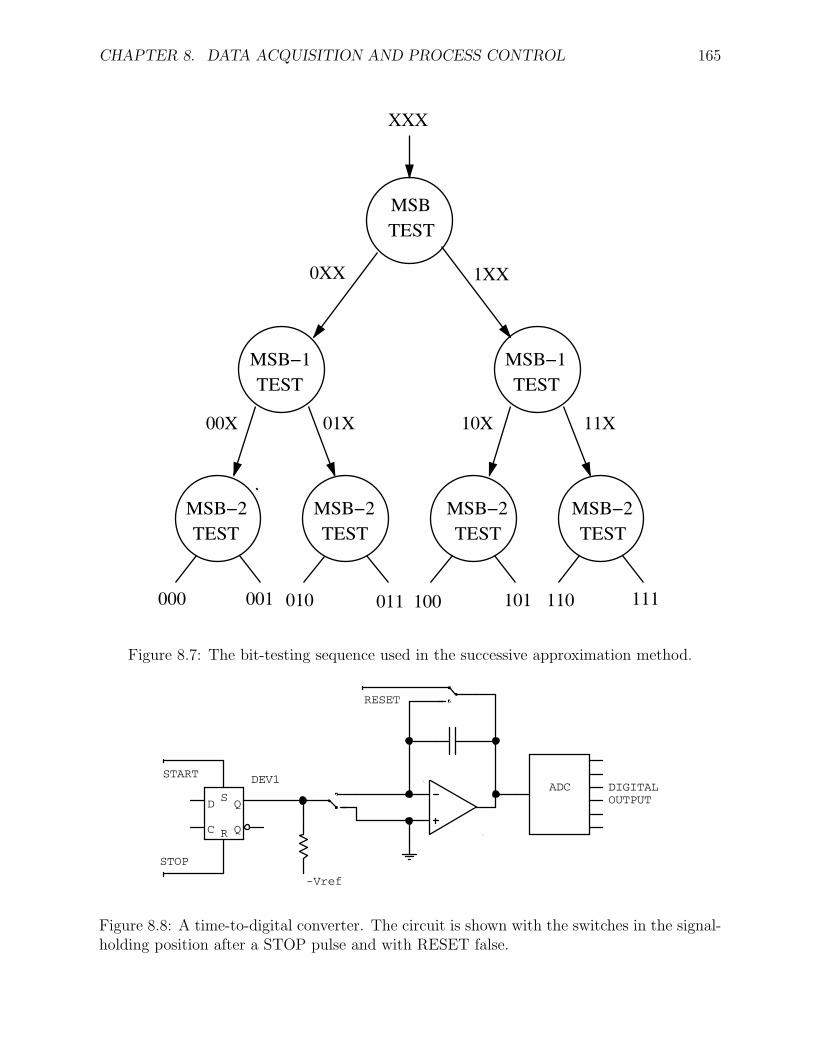
CHAPTER 8. DATA ACQUISITION AND PROCESS CONTROL 165
MSBTEST
MSB−1TEST
MSB−1TEST
MSB−2TEST
MSB−2TEST
MSB−2TEST
MSB−2TEST
XXX
0XX 1XX
00X 01X 10X 11X
000 001 010 011 100 101 110 111
Figure 8.7: The bit-testing sequence used in the successive approximation method.
-Vref
DIGITALOUTPUT
STOP
START
RESET
D
C
S
R
Q
Q
DEV1ADC
Figure 8.8: A time-to-digital converter. The circuit is shown with the switches in the signal-holding position after a STOP pulse and with RESET false.
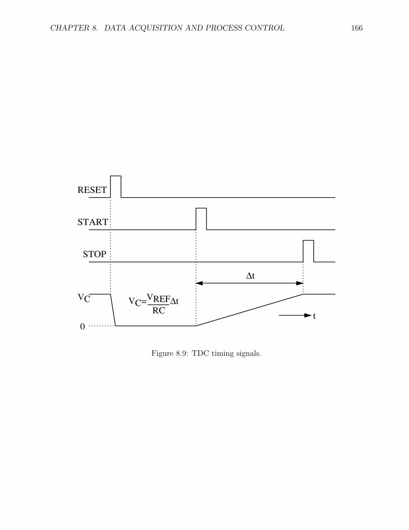
CHAPTER 8. DATA ACQUISITION AND PROCESS CONTROL 166
RESET
START
STOP
VC
0t
∆t
VC=VREF∆tRC
Figure 8.9: TDC timing signals.
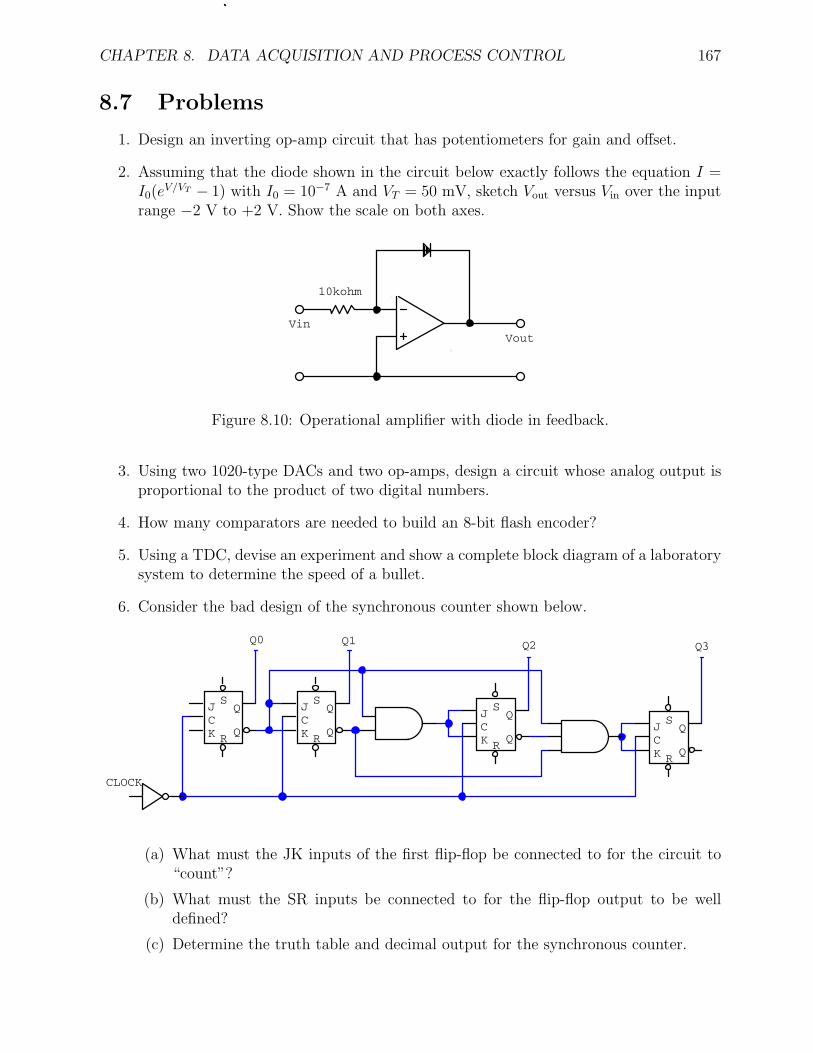
CHAPTER 8. DATA ACQUISITION AND PROCESS CONTROL 167
8.7 Problems
1. Design an inverting op-amp circuit that has potentiometers for gain and offset.
2. Assuming that the diode shown in the circuit below exactly follows the equation I =I0(e
V/VT − 1) with I0 = 10−7 A and VT = 50 mV, sketch Vout versus Vin over the inputrange −2 V to +2 V. Show the scale on both axes.
Vout
10kohm
Vin
Figure 8.10: Operational amplifier with diode in feedback.
3. Using two 1020-type DACs and two op-amps, design a circuit whose analog output isproportional to the product of two digital numbers.
4. How many comparators are needed to build an 8-bit flash encoder?
5. Using a TDC, devise an experiment and show a complete block diagram of a laboratorysystem to determine the speed of a bullet.
6. Consider the bad design of the synchronous counter shown below.
CLOCK
Q0Q3Q2Q1
JCK
S
R
Q
Q
JCK
S
R
Q
Q
JCK
S
R
Q
QJCK
S
R
Q
Q
(a) What must the JK inputs of the first flip-flop be connected to for the circuit to“count”?
(b) What must the SR inputs be connected to for the flip-flop output to be welldefined?
(c) Determine the truth table and decimal output for the synchronous counter.
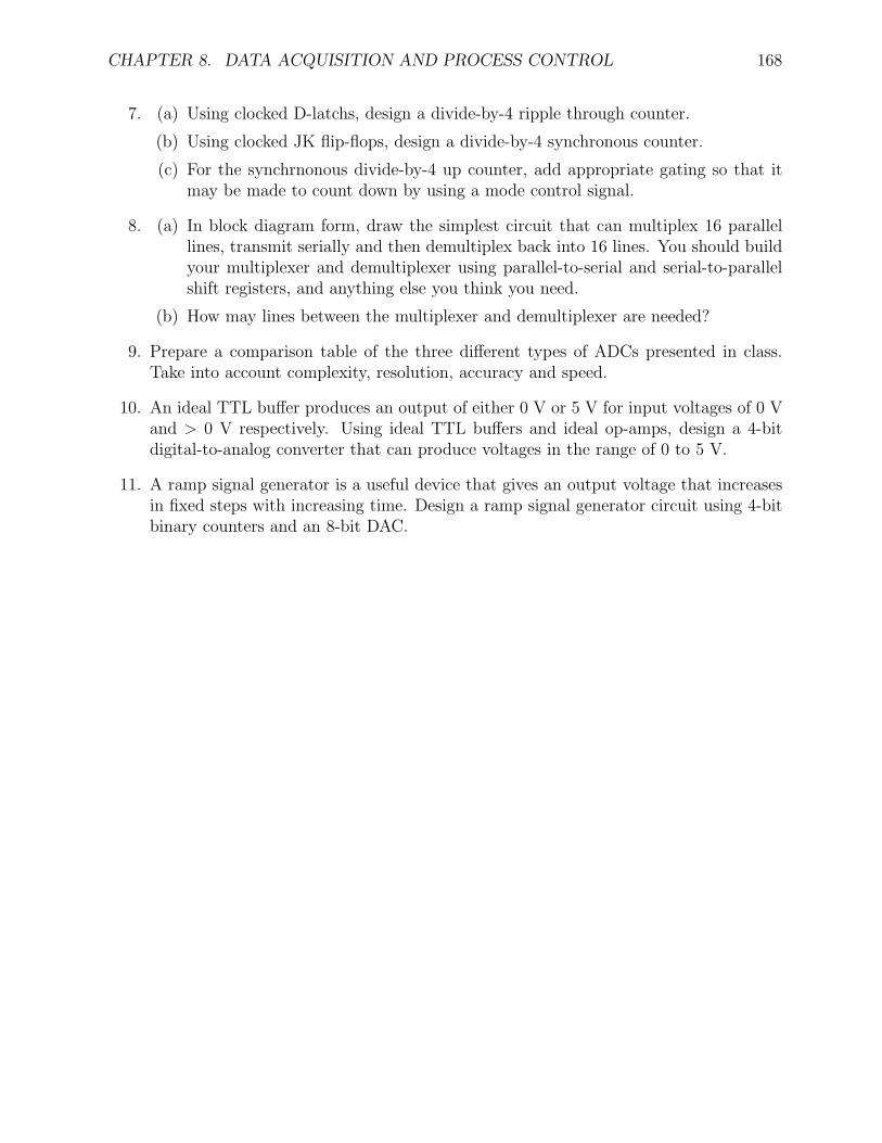
CHAPTER 8. DATA ACQUISITION AND PROCESS CONTROL 168
7. (a) Using clocked D-latchs, design a divide-by-4 ripple through counter.
(b) Using clocked JK flip-flops, design a divide-by-4 synchronous counter.
(c) For the synchrnonous divide-by-4 up counter, add appropriate gating so that itmay be made to count down by using a mode control signal.
8. (a) In block diagram form, draw the simplest circuit that can multiplex 16 parallellines, transmit serially and then demultiplex back into 16 lines. You should buildyour multiplexer and demultiplexer using parallel-to-serial and serial-to-parallelshift registers, and anything else you think you need.
(b) How may lines between the multiplexer and demultiplexer are needed?
9. Prepare a comparison table of the three different types of ADCs presented in class.Take into account complexity, resolution, accuracy and speed.
10. An ideal TTL buffer produces an output of either 0 V or 5 V for input voltages of 0 Vand > 0 V respectively. Using ideal TTL buffers and ideal op-amps, design a 4-bitdigital-to-analog converter that can produce voltages in the range of 0 to 5 V.
11. A ramp signal generator is a useful device that gives an output voltage that increasesin fixed steps with increasing time. Design a ramp signal generator circuit using 4-bitbinary counters and an 8-bit DAC.
Chapter 9
Computers and DeviceInterconnection
These lectures will deal with the interface between computer software and electronic instru-mentation.
9.1 Elements of the Microcomputer
We will treat the microprocessor as just another IC chip on a circuit board. Our stripped-down version will result in a computer suitable to specialized, single-process or single-circuitapplications.
In a typical research laboratory arrangement, the computer would be used to controlequipment, acquire data from the measurement apparatus, perform mathematical operationson the data and make these available on a display device for operator review.
9.1.1 Microprocessor and Microcomputer
The key element of a microcomputer is the LSI microprocessor chip, whose circuitry canacquire, interpret, and execute a sequence of logical and arithmetic instructions. Althoughmost computer programming is done in a high level language, the processor itself deals onlywith binary numbers that represent operation codes (move data, add, subtract, compare,jump, etc.) and addresses (routing information for the data flow) of registers, memorylocations or input/output data ports.
Beside the microprocessor, a complete computer requires a power supply, memory, in-terface circuits to provide ports to external devices, and input/output devices such as akeyboard, display, DACs and ADCs, and magnetic or other (optical) data storage.
9.1.2 Functional Elements of the Computer
The functional elements of a computer are the
• central processing unit (CPU),
169
CHAPTER 9. COMPUTERS AND DEVICE INTERCONNECTION 170
• random access storage (memory), and
• input/output to external devices (I/O).
The sub-units of the CPU are
• instruction decode and CPU control,
• control of addressing for memory and I/O ports,
• data transfer control,
• data and address registers and
• arithmetic logic unit.
To keep track of the CPU steps, the processor maintains a special register, known asthe program counter. The program counter points to (contains the address of) the nextinstruction to be executed. The instruction itself specifies
• the operation to be performed,
• the processor registers to be used and
• possibly data (or a pointer to data in memory).
The CPU will typically perform the following execution cycle:
1. use the program counter to fetch the next instruction.
2. decode the instruction and fetch data from memory into internal registers as required,
3. perform the instruction and put the result in another internal register and
4. set status bits in the status register as required.
The various functional units of the computer are connected by one or more multi-wiredigital buses which pass data, addresses, and control information between the units as shownin figure 9.1.
9.1.3 Mechanical Arrangement
Machines with the lowest cost and highest reliability are generally those with the fewestmechanical connectors and socketed components, while those with more connectors andsockets are more easily expanded and maintained. One design is to have all circuits onmechanically equivalent boards that plug into a common bus, this is the most modulararrangement and is easily maintained. An alternative design is the single-board computerwhich places the CPU and a substantial portion of the memory and I/O interface circuitsonto a single circuit board. This design is more compact and less expensive.
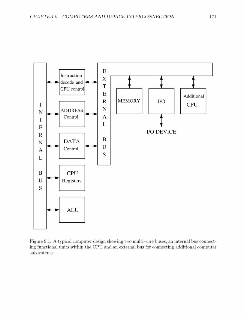
CHAPTER 9. COMPUTERS AND DEVICE INTERCONNECTION 171
I/O
I/O DEVICE
CPUMEMORY
EXTERNAL
BUS
Additional
ALU
DATA
CPU
ADDRESS
Registers
Control
Control
Instruction
decode and
CPU control
INTERNAL
BUS
Figure 9.1: A typical computer design showing two multi-wire buses, an internal bus connect-ing functional units within the CPU and an external bus for connecting additional computersubsystems.
CHAPTER 9. COMPUTERS AND DEVICE INTERCONNECTION 172
9.1.4 Addressing Devices on the Bus
The address determines the destination or source of information. Since the wires of a bus arecommon to all functional units, each unit will see all the data placed on the bus lines. Theaddress lines are used within a receiving unit to determine if available information shouldbe processed or ignored. Each data repository on a common bus will have a unique address.
When the CPU needs to transfer data between itself and a particular location, it imple-ments a sequence of signals as specified by the read or write operation protocol for the bus.The range of numbers that can be represented by the available address lines (wires) on a busis known as the address space. A range of numbers is used mostly to access information frommemory and is thus known as the memory address space. Some processors assign a few ofthese memory addresses to other input/output devices. A feature known as memory-mappedI/O.
9.1.5 Control of the Bus
The information flow on the computer bus is time-multiplexed to allow different functionalunits to use the same bus lines at different times. We will assume that only one device triesto write (drive) a given bus line at any time. A special unit, known as a bus master, hasthe responsibility for controlling the other units, which are correspondingly known as thebus slaves. If several units are capable of becoming bus masters these units must arbitrateamongst themselves to determine which is to have control of the bus for a given interval oftime. Often a direct memory access (DMA) unit is allowed to communicate with a slavememory without going through the CPU bus master. This allows memory access at a higherspeed than having to go through the intermediate CPU bus master.
9.1.6 Clock Lines
The changes of state of all bused signals are synchronized to one or more clock signals, whichare distributed to all functional units on the bus.
Read and write operations between the CPU and memory units are the most common.One approach is for the CPU to set the address lines and data lines and then blindly issuethe control pulses, assuming that the slave unit will respond as needed within the allowedtime. A more elegant but slightly slower technique uses a handshake which requires anacknowledgment response from the slave before proceeding.
9.1.7 Random Access Memory
The random-access memory (RAM) supports both read and write operations. Integratedcircuit RAM comes in two main types:
static RAM in which a single bit of memory is simply a digital flip-flop and requires onlycontinuous power to maintain its state.
CHAPTER 9. COMPUTERS AND DEVICE INTERCONNECTION 173
dynamic RAM in which a bit of memory is a storage capacitor in either the charged ordischarged condition. The term dynamic refers to the need to periodically renew orrefresh the slowly discharging capacitor.
Compared to dynamic memory, static memory has the following advantages. It is simplerto use, about ten times faster and more reliable. On the other hand, it is more expensive,consumes more power and requires more physical space. Because of power consumption inan IC the largest static RAM is 16K bits. The largest dynamic RAM is 260K and hence isused for normal applications while the static RAM is used for special fast applications withinthe same computer. Both types of RAM are volatile, meaning that stored information islost when power is removed from the chip. Some computer designs provide a limited amountof non-volatile read/write RAM storage by using special low-power (and slower) dynamicmemories powered by re-chargeable batteries.
9.1.8 Read-Only Memory
Another form of non-volatile random access storage is the read-only memory (ROM). Herea single memory bit is nothing more than a connection that is either open or closed. Themost common ROM types are known as field-programmable (as opposed to factory pro-grammable). This programming process consists of stepping through all the bits and settingthe necessary ones by burning open the fuse-like material associated with that bit.
There are many varieties of field-programmable ROM units:
PROM – programmable read-only memory,
EPROM – erasable PROM (using ultraviolet light), and
EEPROM (E2PROM) – electrically erasable PROMs.
The most common uses of ROM memory in a computer are to provide initialization suchas memory tests and disk bootstrapping.
9.1.9 I/O Ports
Input and output ports are the pathways by which the CPU communicates with the worldoutside the computer. The pathway may be either
• 1-bit wide (bit-serial),
• 8-bit wide (byte-serial), or
• 16- to 32-bit wide (word-serial).
9.1.10 Interrupts
Real-time applications require the computer to respond immediately to an external stimulus.The hardware interrupt can be used to suspend the current sequence of instructions, performa specific and usually short I/O task, then return to the original sequence of instructions.
CHAPTER 9. COMPUTERS AND DEVICE INTERCONNECTION 174
9.2 8-, 16-, or 32-Bit Busses
A microprocessor can be characterized by the width of its internal and external buses. Thewidth of the internal bus determines the largest number that can be transferred or processedin a single clock cycle. The width of the external bus determines the number of memoryaddresses accessible by the processor. A wider bus is faster and more convenient for theprogrammer. A narrower bus is cheaper and requires simpler external hardware with fewerwires and connections.


![Contenido - Inicio · 14. Transmisión de calor porconvección 395]4.1. Introducción 395 14.2. Coeficientes de transmisión de calor 395 14.2.]. Coeficientes individuales 395](https://img.pdfslide.net/doc/110x75/5ba1c3cd09d3f2666b8d03ce/contenido-14-transmision-de-calor-porconveccion-39541-introduccion.jpg)