Embed Size (px)
Citation preview

PIC32MXPIC32MX Flash Programming Specification
1.0 DEVICE OVERVIEWThis document defines the programming specificationfor the PIC32MX family of 32-bit microcontrollerdevices. This programming specification is designed toguide External Programmer Tools developers. Endcustomers developing applications for PIC32MXdevices should use development tools that alreadyprovide support for device programming.
This document includes programming specificationsfor the PIC32MX family of devices.
2.0 PROGRAMMING OVERVIEWAll PIC32MX devices can be programmed via two pri-mary methods – Self-programming and external toolprogramming. The self-programming method requiresthat the target device already contain executable codewith necessary logic to complete the programmingsequence. The external tool programming method, onthe other hand, does not require any code in the targetdevice – it can program all target devices with or with-out any executable code. This document describes theexternal tool programming method only. Refer to thePIC32MX Family Reference Manual and product datasheet to learn more about the self-programmingmethod.
An external tool programming setup consists of anexternal programmer tool and a target PIC32MXdevice. Figure 2-1 shows the block diagram view of thetypical programming setup. The programmer tool isresponsible for executing necessary programmingsteps and completing the programming operation.
FIGURE 2-1: A PROGRAMMING SYSTEM SETUP
All PIC32MX devices provide two physical interfaces tothe external programmer tool:
• 2-wire In-Circuit Serial Programming™ (ICSP™)• 4-wire JTAG
See Section 4.0 “Connecting to the device” for moreinformation.
Each of these methods may or may not use a down-loadable Program Executive (PE). The PE executesfrom the target device RAM and hides device program-ming details from the programmer. It also removesoverhead associated with data transfer and improvesoverall data throughput. Microchip has developed a PEthat is available for use with any external programmer.See Section 16.0 “The Programming Executive” formore information.
Section 3.0 “Programming Steps” describes highlevel programming steps, followed by detaileddiscussion of each step.
See Appendices for more specific details on EJTAG,programming commands and DC specs.
2.1 AssumptionsBoth 2 and 4-wire interfaces use the EJTAG protocol toexchange data with the programmer. While this docu-ment provides a working description of this protocol asneeded, advanced users are advised to refer to theEJTAG Specification by MIPS Technology, “MD00047”.
Target PIC32MX Device
External CPU
On-Chip Memory
Programmer
© 2008 Microchip Technology Inc. DS61145B-page 1

PIC32MX
3.0 PROGRAMMING STEPSAll programmers must perform a common set of stepsregardless of the actual method they are using.Figure 3-1 shows the steps required to programPIC32MX devices.
FIGURE 3-1: PROGRAMMING FLOW
The following sequence lists each step and provides abrief explanation. Detailed discussion of each step isprovided in following sections.
1. Connect to the target device.
To ensure successful programming, all requiredpins must be connected to appropriate signals.See Section 4.0 “Connecting to the device”for more information.
2. Place the target device in Programming mode.
This step is not required if 4-wire programmingmethod is used. For 2-wire programming meth-ods, the target device must be placed in a spe-cial Programming mode before executingfurther steps. See Section 7.0 “Entering Pro-gramming Mode” for more information.
3. Check the status of the device.
This step checks the status of the device toensure it is ready to receive information from theprogrammer. See Section 8.0 “Check DeviceStatus” for more information.
4. Erase the target device.
If the target memory block in the device is notblank, or the device is code-protected, an erasestep must be performed before programmingany new data. See Section 9.0 “Erasing thedevice” for more information.
5. Enter Programming mode.
This step verifies that the device is not code-pro-tected and boots the TAP controller in order tostart sending and receiving data to the PIC32MXCPU. See 10.0 “Entering Serial executionmode” for more information.
6. Download the Programming Executive (PE).
This step is not required if a method that doesnot require PE is used. The PE is a small blockof executable code that is first downloaded intothe RAM of the target device, which in turnreceives and programs the actual data. See 11.0“Downloading the Programming Executive(PE)” for more information.
7. Download the block of data to program.
All methods with or without PE must downloadthe desired programming data into a block ofmemory in RAM. See 12.0 “Downloading aData Block” for more information.
8. Initiate Flash Write.
After downloading each block of data into RAM,the programming sequence must be started toprogram it into the target device’s Flash mem-ory. See 13.0 “Initiating a Flash ROW Write”for more information.
9. Repeat steps 7 and 8 until all data blocks aredownloaded and programmed.
Done
Exit Programming Mode
Verify Device
Done
Initiate Flash Write
Download a Data Block
Download PE(*Optional)
Enter Serial Exec Mode
Erase Device
Check Device Status
Start
Enter Enhanced ICSP™(*Only required for 2-wire)
No
Yes
DS61145B-page 2 © 2008 Microchip Technology Inc.

PIC32MX
10. Verify the program memory.After all programming data and Configurationbits are programmed, the target device memoryshould be read back and verified for the match-ing content. See 14.0 “Verify Device Memory”for more information.
11. Exit the Programming mode.
The newly programmed data is not effective untileither power is removed and reapplied to the tar-get device or an exit programming sequence isperformed. See 15.0 “Exiting ProgrammingMode” for more information.
4.0 CONNECTING TO THE DEVICEThe PIC32MX family provides two possible physicalinterfaces for connecting to and programming thememory contents (Figure 4-1). For all programminginterfaces, the target device must be properly poweredand all required signals must be connected.
FIGURE 4-1: PROGRAMMING INTERFACES
4.1 4-Wire InterfaceOne possible interface is the 4-wire JTAG (IEEE1149.1) port. Table 4-1 lists the required pin connec-tions. This interface uses the following 4 communica-tion lines to transfer data to and from the PIC32MXdevice being programmed:
• TCK – Test Clock Input• TMS – Test Mode Select Input• TDI – Test Data input• TDO – Test Data output
These signals are described in detail below. Refer tothe data sheet of the particular device for theconnection of the signals to chip pins.
4.1.1 TEST CLOCK INPUT (TCK)TCK is the clock that controls the updating of the TAPcontroller and the shifting of data through the instruc-tion or selected data register(s). TCK is independent ofthe processor clock with respect to both frequency andphase.
4.1.2 TEST MODE SELECT INPUT (TMS)TMS is the control signal for the TAP controller. Thissignal is sampled on the rising edge of TCK.
4.1.3 TEST DATA INPUT (TDI)TDI is the test data input to the instruction or selecteddata register(s). This signal is sampled on the risingedge of TCK for some TAP controller states.
4.1.4 TEST DATA OUTPUT (TDO)TDO is the test data output from the instruction or dataregister(s). This signal changes on the falling edge ofTCK. TDO is only driven when data is shifted out,otherwise the TDO is tri-stated.
TABLE 4-1: 4-WIRE INTERFACE PINS
Programmer
2-WireICSP™
OR
4-WireJTAG
+ MCLR, VDD, VSS
PIC32
Pin NamePin Name Pin Type Pin Description
MCLR MCLR P Programming EnableENVREG ENVREG I Enable for On-Chip Voltage RegulatorVDD and AVDD(1) VDD P Power SupplyVSS and AVSS(1) VSS P GroundVDDCORE VDDCORE P Regulated Power Supply for CoreTDI TDI I Test Data InTDO TDO O Test Data OutTCK TCK I Test ClockTMS TMS I Test Mode StateLegend: I = Input, O = Output, P = PowerNote 1: All power supply and ground pins must be connected, including analog supplies (AVDD) and ground
(AVSS).
© 2008 Microchip Technology Inc. DS61145B-page 3

PIC32MX
4.2 2-Wire InterfaceAnother possible interface is the 2-wire ICSP port.Table 4-2 lists the required pin connections. This inter-face uses the following 2 communication lines to trans-fer data to and from the PIC32MX device beingprogrammed:• PGCx – Serial Program Clock.• PGDx – Serial Program Data.
These signals are described in detail below. Refer tothe data sheet of the particular device for the connec-tion of the signals to chip pins.
4.2.1 SERIAL PROGRAM CLOCK (PGCX)PGCx is the clock that controls the updating of the TAPcontroller and the shifting of data through the instruc-tion or selected data register(s). PGCx is independentof the processor clock, with respect to both frequencyand phase.
4.2.2 SERIAL PROGRAM DATA (PGDX)PGDx is the data input/output to the instruction orselected data register(s), it is also the control signal forthe TAP controller. This signal is sampled on the fallingedge of PGC for some TAP controller states.
TABLE 4-2: 2-WIRE INTERFACE PINS
Pin NamePin Name Pin Type Pin Description
MCLR MCLR P Programming EnableENVREG ENVREG I Enable for On-Chip Voltage RegulatorVDD and AVDD(1) VDD P Power SupplyVSS and AVSS(1) VSS P GroundVDDCORE VDDCORE P Regulated Power Supply for CorePGC1 PGC I Primary Programming Pin Pair: Serial Clock PGD1 PGD I/O Primary Programming Pin Pair: Serial Data PGC2 PGC I Secondary Programming Pin Pair: Serial Clock PGD2 PGD I/O Secondary Programming Pin Pair: Serial Data Legend: I = Input, O = Output, P = PowerNote 1: All power supply and ground pins must be connected, including analog supplies (AVDD) and ground
(AVSS).
DS61145B-page 4 © 2008 Microchip Technology Inc.

PIC32MX
4.3 Power RequirementsAll devices in the PIC32MX family are dual voltagesupply designs: one supply for the core and peripheralsand another for the I/O pins. Some devices contain anon-chip regulator to alleviate the need for two externalvoltage supplies.All of the PIC32MX devices power their core digitallogic at a nominal 1.8V. This may create an issue fordesigns that are required to operate at a higher typicalvoltage, such as 3.3V. To simplify system design, alldevices in the PIC32MX family incorporate an on-chipregulator that allows the device to run its core logic fromVDD.
The regulator provides power to the core from the otherVDD pins. A low ESR capacitor (such as tantalum) mustbe connected to the VDDCORE pin (Figure 4-2). Thishelps to maintain the stability of the regulator. Thespecifications for core voltage and capacitance arelisted in Section 20.0 “Appendix C: AC/DC Charac-teristics and Timing Requirements”.
FIGURE 4-2: CONNECTIONS FOR THE ON-CHIP REGULATOR
VDD
ENVREG
VDDCORE/VCAP
VSS
PIC32MX3.3V(1)1.8V(1)
VDD
ENVREG
VDDCORE/VCAP
VSS
PIC32MX
CEFC
3.3V
Regulator Enabled (ENVREG tied to VDD):
Regulator Disabled (ENVREG tied to ground):
(10 μF typ)
Note 1: These are typical operating voltages. Refer to Section 20.0 “Appendix C: AC/DC Char-acteristics and Timing Requirements” for the full operating ranges of VDD and VDDCORE.
© 2008 Microchip Technology Inc. DS61145B-page 5

PIC32MX
5.0 EJTAG vs. ICSPProgramming is accomplished via the EJTAG modulein the CPU core. EJTAG is connected to either the fullset of JTAG pins, or a reduced 2-wire to 4-wire EJTAGinterface. In both modes, programming of the PIC32MXFlash memory is accomplished through the ETAPcontroller. The TAP Controller uses the TMS pin todetermine if instruction or data registers should beaccessed in the shift path between TDI and TDO (seeFigure 5-1).
FIGURE 5-1: TAP CONTROLLER
The basic concept of EJTAG that is used for program-ming is the use of a special memory area calledDMSEG (FF200000h-FF2FFFFFh) which is only avail-able when the processor is running in DEBUG mode.All instructions are serially shifted into an internalbuffer, then loaded into the instruction register and exe-cuted by the CPU. Instructions are fed through theETAP State machine 32 bits at a time.
FIGURE 5-2: BASIC PIC32MX PROGRAMMING BLOCK
2-Wire to 4-Wire:Converts 2-wire ICSP interface to 4-wire JTAG.
• ETAP- Serially feeds instructions and data into CPU.
• MTAP- In addition to the EJTAG TAP (ETAP) control-
ler, the PIC32MX device uses a second proprietary TAP controller for additional oper-ations. The Microchip TAP (MTAP) controller supports two instructions relevant to pro-gramming. These are the MTAP_COMMAND and MTAP_SWTAP instructions, see Table 19-1 for complete list of commands. The MTAP_COMMAND instruction provides a mechanism for a JTAG probe to send com-mands to the device via its data register.
- The programmer sends commands by shift-ing in the MTAP_COMMAND instruction via the SendCommand pseudo op, and then sending MTAP_COMMAND DR Commands via XferData psuedo op (see Table 19-2 for specific com-mands). The probe does not need to issue an MTAP_COMMAND instruction for every com-mand shifted into the data register.
• CPU- The CPU executes instructions at 8 MHz via
the internal oscillator.• Flash Controller
- The Flash Controller controls erasing and programming of the Flash memory on the device.
• Flash Memory- The PIC32MX device Flash memory is
divided into two logical Flash partitions con-sisting of the Boot Flash Memory (BFM) and Program Flash Memory (PFM). The Boot Flash Memory (BFM) map extends from 1FC00000h to 1FC02FFFh, and the Program Flash Memory (PFM) map extends from 1D000000h to 1D07FFFFh. Code storage begins with the BFM and supports up to 12K bytes, then continues with the PFM which supports up to 512K bytes. Table 5-1 shows the program memory size of each device variant. Each erase block, or page, contains 1K instructions (4 KBytes), and each program block, or row, contains 128 instructions (512 Bytes).
- The last four implemented program memory locations in BFM are reserved for the Device Configuration registers.
TMS
TCK
TDOTDI
Tap Controller
Instruction, Data and ControlRegisters
CommonVDD
VSS
MCLR
TMS
TCK
TDI
TDO
OR
PGC
PGD
ETAP CPU
MTAP
2-W
Flash
Flashto
4-W
Controller
Memory
DS61145B-page 6 © 2008 Microchip Technology Inc.

PIC32MX
TABLE 5-1: CODE MEMORY SIZE5.1 4-Wire JTAG DetailsThe 4-wire interface uses standard JTAG (IEEE1149.1) interface signals.
• TCK: Test Clock drives data in/out• TMS: Test Mode Select – Selects operational
mode• TDI: Test Data In – Data into the device• TDO: Test Data Out – Data out of the device
Since only one data line is available, the protocol isnecessarily serial, like SPI. The clock input is at theTCK pin. Configuration is performed by manipulating astate machine one bit at a time through TMS pin. Onebit of data is transferred in and out per TCK clock pulseat the TDI and TDO pins, respectively. Different instruc-tion modes can be loaded to read the chip ID or manip-ulate chip functions.
Data presented to TDI must be valid for a chip specificsetup time before, and hold time after the rising edge ofTCK. TDO data is valid for a chip specific time after thefalling edge of TCK. Refer to Figure 5-3.
FIGURE 5-3: 4-WIRE JTAG INTERFACE
5.2 2-wire ICSP DetailsWhen in this mode the 2-wire ICSP signals are timemultiplexed into the 2-wire to 4-wire block. The 2-wireto 4-wire block then converts the signals to look like a4-wire JTAG port to the TAP controller.
There are two possible modes of operation:
• 4-Phase ICSP• 2-Phase ICSP
5.2.1 4-PHASE ICSPIn 4-Phase ICSP, TDI, TDO, and TMS are multiplexedonto PGD in 4 clocks (see Figure 5-4). The Least Sig-nificant bit (LSb) is shifted first, and TDI and TMS aresampled on the falling edge of PGC while TDO isdriven on the falling edge of PGC. 4-Phase mode isused for both read and write data transfers.
PIC32MX Device Boot Flash Memory Address (Bytes) Program Flash Memory Address(Bytes)
PIC32MX300F032H 1FC00000h-1FC02FFFh (12KB) 1D000000h-1D007FFFh (32KB)PIC32MX320F064H 1FC00000h-1FC02FFFh (12KB) 1D000000h-1D00FFFFh (64KB)PIC32MX320F128H 1FC00000h-1FC02FFFh (12KB) 1D000000h-1D01FFFFh (128KB)PIC32MX340F256H 1FC00000h-1FC02FFFh (12KB) 1D000000h-1D03FFFFh (256KB)PIC32MX320F128L 1FC00000h-1FC02FFFh (12KB) 1D000000h-1D01FFFFh (128KB)PIC32MX360F256L 1FC00000h-1FC02FFFh(12KB) 1D000000h-1D03FFFFh(256KB)PIC32MX360F512L 1FC00000h-1FC02FFFh(12KB) 1D000000h-1D07FFFFh(512KB)
TMS
TDI
TDO
iMSbiLSb
‘1’
TCK
oLSb oMSb
‘1’ ‘1’ ‘1’‘0’ ‘0’ ‘0’
© 2008 Microchip Technology Inc. DS61145B-page 7

PIC32MX
FIGURE 5-4: 2-WIRE, 4-PHASE5.2.2 2-PHASE ICSPIn 2-Phase ICS, TMS and TDI are multiplexed intoPGD in 2 clocks (see Figure 5-5). The LSb is shiftedfirst, and TDI and TMS are sampled on the falling edgeof PGC. There is no TDO output provided in this mode.This mode was designed to accelerate 2-Wire,write-only transactions.
TMS
TDI
TDO
IR4IR0
‘1’
TCK
‘1’ ‘1’ ‘1’‘0’ ‘0’ ‘0’
X1
PGC
PGD pTDO = 1 TDI = IR0 TMS = 0 nTDO = 0
Note: The packet is NOT actually executed untilthe first clock of the next packet.
DS61145B-page 8 © 2008 Microchip Technology Inc.

PIC32MX
FIGURE 5-5: 2-WIRE, 2-PHASETMS
TDI
TDO
IR4IR0
‘1’
TCK
‘1’ ‘1’ ‘1’‘0’ ‘0’ ‘0’
X1
PGC
PGD TDI = IR0 TMS = 0
© 2008 Microchip Technology Inc. DS61145B-page 9

PIC32MX
6.0 PSEUDO OPERATIONSTo simplify the description of programming details, alloperations will be described using pseudo operations.There are several functions used in the pseudocodedescriptions. These are used either to make thepseudocode more readable, to abstract implementa-tion-specific behavior, or both. When passing parame-ters with pseudo operation, the following syntax will beused: 5’h0x03 (i.e.,send 5 bit hex value 0x03). Thesefunctions are defined in this section, and include thefollowing:
• SetMode (mode)• SendCommand (command)• oData = XferData (iData)• oData = XferFastData (iData)• oData = XferInstruction (instruction)
6.1 SetMode Pseudo OperationFormat: SetMode (mode)Purpose:To set the EJTAG state machine to a specific state.
Description:The value of mode is clocked into the device on signalTMS. TDI is set to a ‘0’ and TDO is ignored.
Restrictions:None.
Example:
SetMode(6’b011111)
FIGURE 6-1: SetMode 4-WIRE
FIGURE 6-2: SetMode 2-WIRE
TMS
TDI
TDO
‘1’
TCK
‘1’ ‘1’‘1’ ‘1’ ‘0’
Mode = 6’b011111
PGD
PGC
TDI = 0 TDO = 1TMS = 1 TDI = 0 TMS = 0 TDO = X
Mode = 6’b011111
DS61145B-page 10 © 2008 Microchip Technology Inc.

PIC32MX
6.2 SendCommand Pseudo OperationFormat: SendCommand (command)Purpose:To send a command to select a specific TAP register.Description:First the TMS Header is clocked into the device toselect the Shift IR state. The Command is then clockedinto the device on TDI while holding signal TMS low.The last Most Significant bit (MSb) of the command isthen clocked in while setting TMS ‘high’. Finally, theTMS Footer is clocked in on TMS to return the TAPcontroller to the Run/Test Idle state.
Restrictions:None.
Example:
SendCommand (5’h07)
FIGURE 6-3: SendCommand 4-WIRE
FIGURE 6-4: SendCommand 2-WIRE
TMS
TDI
TDO
iMSb
‘1’
TCK
‘1’ ‘1’ ‘1’‘0’ ‘0’ ‘0’
X1
iLSb
TMS Header = 1100 Command = 5’h07Command (MSb)
+ TMS = 1 TMS Footer = 10
PGD
PGC
TDI = 0 TMS = 1 TMS = 1TDI = 0TDO = X TDO = XTDI=iMSbTDO = XTMS = 0TDI=iLSbTDO = XTMS = 1
TMS Header = 1100 Command (5’h07) + TMS = 0 Command (MSb) + TMS = 1 TMS Footer = 10
© 2008 Microchip Technology Inc. DS61145B-page 11

PIC32MX
6.3 XferData Pseudo OperationFormat: oData = XferData (iData)Purpose:To clock data to and from the register selected by thecommand.Description:First the TMS Header is clocked into the device toselect the Shift DR state. The Data is then clockedin/out of the device on TDI/TDO while holding signalTMS low. The last MSb of the data is then clockedin/out while setting TMS ‘high’. Finally, the TMS Footeris clocked in on TMS to return the TAP controller to theRun/Test Idle state.
Restrictions:None.
Example:
oData = XferData (32’h12)
FIGURE 6-5: XferData 4-WIRE
FIGURE 6-6: XferData 2-WIRE (4-PHASE)
TMS
TDI
TDO
iMSb
‘1’
TCK
‘1’ ‘1’‘0’ ‘0’ ‘0’
iLSb
TMS Header = 100 Data (32’h12)Data (MSb)
+ TMS = 1 TMS Footer = 10
oMSboLSb
TDI = 0 TMS = 0 TDO = oLSbTDI = 0TDO = XTMS = 0TDI = 0TDO = XTMS = 1
PGC
PGD
TMS Header = 100
TDI = 0 TMS = 0 TDO = XTDI = 0TDO = XTMS = 1
TMS = 1 TDO = XTMS = 0TDI = iLSb TDO = oLSb+1 TDI = iMSb
Data (31’h12) + TMS = 0 Data (MSb) + TMS Footer = 1
TMS Footer = 10
...
DS61145B-page 12 © 2008 Microchip Technology Inc.

PIC32MX
6.4 XferFastData Pseudo OperationFormat: oData = XferFastData (iData)Purpose:To send 32 bits of data in/out of the device fast.Description:First the TMS Header is clocked into the device toselect the Shift DR state. For 2-wire (4-phase), notethat on the last clock, oPrAcc bit is shifted out on TDOwhile clocking in the TMS Header. If the value ofoPrAcc is not ‘1’, then the whole operation must berepeated. Next, the input value of PrAcc bit, which is ‘0’,is clocked in. For 2-wire (4-phase), the TDO during thisoperation will be the LSbit of out output. The rest of the31-bits of the input data is clocked in and the 31-bits ofoutput data is clocked out. For the last bit of the inputdata, the TMS Footer = 1 is set. Finally, TMS Footer =10 is clocked in to return the TAP controller to theRun/Test Idle state.
Restrictions:The SendCommand (ETAP_FASTDATA) must be sentfirst to select the Fastdata register. See Table 19-4 forcomplete description of commands.
The 2-Phase XferData is only used when talking to thePE. See Section 16.0 “The Programming Execu-tive” for more details.
Example:
FIGURE 6-7: XferFastdata 4-WIRE
FIGURE 6-8: XferFastdata 2-WIRE (2-PHASE)
// Select the Fast Data Register
SendCommand(ETAP_FASTDATA)
// Send/Receive 32-bit Data
oData = XferFastData(32’h12)
TMS
TDI
TDO
iMSbiLSb
‘1’
TCK
oLSb oMSb
‘1’ ‘1’‘0’ ‘0’ ‘0’
‘0’
‘1’
TMS Header = 100 PrAcc Data (32’h12)Data (MSb) +
TMS = 1 TMS Footer = 10
TDI = X TMS = 1TDI = XTDI =TMS = 0TDO =TMS = 0TDI = 0TMS = 1
TMS Header = 100 Data (32’h12) TMS Footer = 10
iLSbPGD
PGC
PrAcc
TMS = 1 MSb
Data (MSb) TMS = 1
© 2008 Microchip Technology Inc. DS61145B-page 13

PIC32MX
FIGURE 6-9: XferFastData 2-WIRE (4-PHASE)TDI = 0 TMS = 0 TDO = 1TDI = 0TDO = XTMS = 0TDI = 0TDO = XTMS = 1
PGC
PGD
TMS Header = 100
TDI = 0 TMS = 0 TDO = XTDI = 0TDO = XTMS = 1
TMS = 1 TDO = oMSbTMS = 0TDI = iLSb TDO = oLSb+1 TDI = iMSb
Data (31’h12) + TMS = 0 Data (MSb) + TMS Footer = 1
TMS Footer = 10
...TMS = 0TDI = 0 TDO = oLSb
PrAcc
...
DS61145B-page 14 © 2008 Microchip Technology Inc.

PIC32MX
6.5 XferInstruction Pseudo OperationFormat: XferInstruction (instruction)Purpose:To send 32 bits of data for the device to execute.Description:The instruction is clocked into the device and thenexecuted by CPU.
Restrictions:The device must be in Debug mode.
EXAMPLE 6-1: XferInstruction EXAMPLE XferInstruction (instruction)
{
// Select Control Register
SendCommand(ETAP_CONTROL);
// Wait until CPU is ready
// Check if Processor Access bit (bit 18) is set
do {
controlVal = XferData(32’h0x0004C000);
} while( PrAcc(contorlVal<18>) is not ‘1’ );
// Select Data Register
SendCommand(ETAP_DATA);
// Send the instruction
XferData(instruction);
// Tell CPU to execute instruction
SendCommand(ETAP_CONTROL);
XferData(32’h0x0000C000);
}
© 2008 Microchip Technology Inc. DS61145B-page 15

PIC32MX
7.0 ENTERING PROGRAMMING MODE
This step is not required if a 4-wire programmingmethod is used. For 2-wire programming methods, thetarget device must be placed in a special Programmingmode before executing further steps.
The following steps are required to enter Programmingmode:
1. The MCLR pin is briefly driven high, then low.2. A 32-bit key sequence is clocked into PGDx.3. Finally, MCLR is then driven high within a spec-
ified period of time and held.
Please refer to 20.0 “Appendix C: AC/DC Character-istics and Timing Requirements” for timingrequirements.
The programming voltage applied to MCLR is VIH,which is essentially VDD in the case of PIC32MXdevices. There is no minimum time requirement for
holding at VIH. After VIH is removed, an interval of atleast P16 must elapse before presenting the keysequence on PGDx.
The key sequence is a specific 32-bit pattern:‘0100 1101 0100 0011 0100 1000 0101 0000’(more easily remembered as ascii ‘MCHP’). The devicewill enter Program/Verify mode only if the keysequence is valid. The Most Significant bit (MSb) of theMost Significant nibble must be shifted in first.
Once the key sequence is complete, VIH must beapplied to MCLR and held at that level for as long asProgramming mode is to be maintained. An interval ofat least time P17 and P7 must elapse before presentingdata on PGDx. Signals appearing on PGDx before P7has elapsed will not be interpreted as valid.
Upon successful entry, the program memory can beaccessed and programmed in serial fashion. While inthe Programming mode, all unused I/Os are placed inthe high-impedance state.
FIGURE 7-1: ENTERING ENHANCED ICSP™ MODE
MCLR
PGDx
PGCx
VDD
P6P14
b31 b30 b29 b28 b27 b2 b1 b0b3...
Program/Verify Entry Code = 4D434850h
P2BP2A
P16
P17
0 1 0 0 1 0 0 0 0
P7VIH VIH
DS61145B-page 16 © 2008 Microchip Technology Inc.

PIC32MX
8.0 CHECK DEVICE STATUSBefore a device can be programmed, the programmermust check the status of the device to ensure it is readyto receive information.
FIGURE 8-1: CHECK DEVICE STATUS
8.1 4-Wire InterfaceFour wire JTAG programming is a Mission mode oper-ation and therefore the setup sequence to begin pro-graming should be done while asserting MCLR.Holding the device in Reset prevents the processorfrom executing instructions or driving ports.
The following steps are required to check the devicestatus using the 4-wire interface:
1. Set MCLR pin low.2. SetMode (6’b011111) to force the Chip TAP
controller into RUN TEST/IDLE state.3. SendCommand (MTAP_SW_MTAP)4. SendCommand (MTAP_COMMAND)5. statusVal = XferData (MCHP_STATUS).6. If CFGRDY (statusVal<3>) is not ‘1’ and
FCBUSY (statusVal<2>) is not ‘0’ GOTO step 5.
8.2 2-Wire InterfaceThe following steps are required to check the devicestatus using the 2-wire interface:
1. SetMode (6’b011111) to force the Chip TAPcontroller into RUN TEST/IDLE state.
2. SendCommand (MTAP_SW_MTAP)3. SendCommand (MTAP_COMMAND)4. statusVal = XferData (MCHP_STATUS).5. If CFGRDY (statusVal<3>) is not ‘1’ and
FCBUSY (statusVal<2>) is not ‘0’ GOTO step 4.
4-WireSet MCLR low
SetMode (6’b011111)
SendCommand (MTAP_SW_MTAP)
SendCommand (MTAP_COMMAND)
statusVal = XferData (MCHP_STATUS)
FCBUSY = 0CFGRDY = 1
No
Note: If CFGRDY and FCBUSY do not come tothe proper state within 10 ms, thesequence may have been executed wrongor the device is damaged.
© 2008 Microchip Technology Inc. DS61145B-page 17

PIC32MX
9.0 ERASING THE DEVICEBefore a device can be programmed, it must beerased. The erase operation writes all ‘1’s to the flashmemory and prepares it to program a new set of data.Once a device is erased, it can be verified by perform-ing a “Blank Check” operation. See Section 9.1“Blank Check” for more information.
The procedure for erasing program memory (Program,Boot, and Configuration memory) consists of selectingthe MTAP and sending the MCHP_ERASE command.The programmer then must wait for the erase operationto complete by reading and verifying bits in theMCHP_STATUS value. Figure 9-1 shows the process forperforming a Chip Erase.
FIGURE 9-1: ERASE DEVICE
The following steps are required to erase a targetdevice:
1. SendCommand (MTAP_SW_MTAP).2. SendCommand (MTAP_COMMAND).3. XferData (MCHP_ERASE).4. statusVal = XferData (MCHP_STATUS). 5. If CFGRDY (statusVal<3>) is not ‘1’ and
FCBUSY (statusVal<4>) is not ‘0’ GOTO to step 4.
.
9.1 Blank CheckThe term “Blank Check” implies verifying that thedevice has been successfully erased and has noprogrammed memory locations. A blank or erasedmemory location is always read as ‘1’.
The device Configuration registers are ignored by theBlank Check. Additionally, all unimplemented memoryspace should be ignored from the Blank Check.
Note: The Device ID memory locations areread-only and can not be erased. Thus,Chip Erase has no effect on these memorylocations.
SendCommand (MTAP_COMMAND)
statusVal = XferData (MCHP_STATUS)
FCBUSY = 0CFGRDY = 1
NO
SendCommand (MTAP_SW_MTAP)
Select MTAP
Put MTAP in Command Mode
XferData (MCHP_ERASE)
Issue Chip Erase Command
Read Erase Status
Note: The Chip Erase operation is a self-timedoperation. If the FCBUSY and CFGRDYbits do not become properly set within thespecified Chip Erase time, the sequencemay have been executed wrong or thedevice is damaged.
DS61145B-page 18 © 2008 Microchip Technology Inc.

PIC32MX
10.0 ENTERING SERIAL EXECUTION MODE
Before a device can be programmed, it must be placedin Serial Execution mode.
The procedure for entering Serial Execution mode con-sists of verifying the device in not code-protected, if thedevice is code-protected a Chip Erase must be per-formed see Section 9.0 “Erasing the device” fordetails.
FIGURE 10-1: ENTERING SERIAL EXECUTION MODE
10.1 4-Wire InterfaceThe following steps are required to enter SerialExecution mode:
1. SendCommand (MTAP_SW_MTAP).2. SendCommand (MTAP_COMMAND).3. statusVal = XferData (MCHP_STATUS). 4. If CPS (statusVal<7>) is not ‘1’ the device must
be erased first.5. SendCommand (MTAP_SW_ETAP).6. SendCommand (ETAP_EJTAGBOOT).7. Set MCLR ‘High’.
10.2 2-wire InterfaceThe following steps are required to enter SerialExecution mode:
1. SendCommand (MTAP_SW_MTAP).2. SendCommand (MTAP_COMMAND).3. statusVal = XferData (MCHP_STATUS). 4. If CPS (statusVal<7>) is not ‘1’ the device must
be erased first.5. XferData (MCHP_ASSERT_RST).6. SendCommand (MTAP_SW_ETAP).7. SendCommand (ETAP_EJTAGBOOT).8. SendCommand (MTAP_SW_MTAP).9. SendCommand (MTAP_COMMAND).10. XferData (MCHP_DE_ASSERT_RST).11. XferData (MCHP_EN_FLASH).
Select MTAPSendCommand (MTAP_SW_MTAP)
Put MTAP in Command ModeSendCommand (MTAP_COMMAND)
Read Code-Protect StatusstatusVal-XferData (MCHP_STATUS)
CPS = 1Cannot Enter
Must Erase First
Assert Reset2-WireXferData (MCHP_ASSERT_RST)
Select ETAPSendCommand (MTAP_SW_ETAP)
Put CPU in Serial Exec ModeSendCommand (ETAP_EJTAGBOOT)
Set MCLR High
4-Wire
Select MTAPSendCommand (MTAP_SW_MTAP)
Put MTAP in Command ModeSendCommand (MTAP_COMMAND)
No
Release ResetXferData (MCHP_DE_ASSERT_RST)
Enable FlashXferData (MCHP_EN_FLASH)
2-Wire
© 2008 Microchip Technology Inc. DS61145B-page 19

PIC32MX
/
0. is
c-ws:
the the
-0 ign c-
f
s
11.0 DOWNLOADING THE PROGRAMMING EXECUTIVE (PE)
The programming executive resides in RAM memoryand is executed by CPU to program the device. Theprogramming executive provides the mechanism forthe programmer to program and verify PIC32MXdevices using a simple command set and communica-tion protocol. There are several basic functionsprovided by the programming executive:
• Read Memory• Erase Memory• Program Memory• Blank Check• Read Executive Firmware Revision• Get CRC of Flash Memory Locations
The programming executive performs the low-leveltasks required for programming and verifying a device.This allows the programmer to program the device byissuing the appropriate commands and data. A detaileddescription for each command is provided inSection 16.2 “Programming Executive CommandSet”.
The programming executive uses the device’s dataRAM for variable storage and program execution. Afterthe programming executive has run, no assumptionsshould be made about the contents of data RAM.
After the programming executive is loaded into the dataRAM, the PIC32MX family can be programmed usingthe command set shown in Table 16-1.
FIGURE 11-1: DOWNLOAD PE
Loading the programming executive in the memory is atwo step process:
1. Load the PE loader in the data RAM. (The PEloader loads the programming executive binaryfile in the proper location of the data RAM, andwhen done, jumps to the programming exec andstarts executing it.)
2. Feed the programming executive binary to thePE loader.
The following steps are required to download theprogramming executive:
Write PE Loader to RAM
Load PE
TABLE 11-1: DOWNLOAD PROGRAM EXEC
Operation OperandStep 1: Initialize BMXCON to 0x1f0040. The instruction sequence executed by the PIC32MX core is as follows: lui a0,0xbf88ori a0,a0,0x2000 /* address of BMXCON */lui a1,0x1fori a1,a1,0x40 /* $a1 has 0x1f0040 */sw a1,0(a0) /* BMXCON initialized *
XferInstruction 0x3c04bf88XferInstruction 0x34842000XferInstruction 0x3c05001fXferInstruction 0x34a50040XferInstruction 0xac850000
Step 2: Initialize BMXDKPBA to 0x800. The instruction sequence executed by the PIC32MX core is as follows:li a1,0x800sw a1,16(a0)
XferInstruction 0x34050800XferInstruction 0xac850010Step 3: Initialize BMXDUDBA and BMXDUPBA to 0x800The instruction sequence executed by the PIC32MX coreas follows:li a1,0x8000sw a1,32(a0)sw a1,48(a0)
XferInstruction 0x34058000XferInstruction 0xac850020XferInstruction 0xac850030Step 4: Setup PIC32MX RAM address for PE. The instrution sequence executed by the PIC32MX core is as follolui a0,0xa000ori a0,a0,0x800
XferInstruction 0x3c04a000XferInstruction 0x34840800Step 5: Load PE_Loader. Repeat this step (step 5) until entire PE_Loader is loaded in the PIC32MX memory. In operands field, “<PE_loader hi++>” represents the MSbs31-to-16 of the PE loader opcodes shown in Table 11.2. Likewise, “<PE_loader lo++>” represents the LSbs 15-toof the PE loader opcodes shown in Table 11.2. The “++” sindicates that when these operations are performed in sucession, the new word is to be transferred from the list oopcodes of the LPE Loader shown in Table 11.2. The instruction sequence executed by the PIC32MX core is afollows:lui a2, <PE_loader hi++>ori a0,a0, <PE_loader lo++>sw a2,0(a0)addiu a0,a0,4
DS61145B-page 20 © 2008 Microchip Technology Inc.

PIC32MX
XferInstruction (0x3c06 <PE_loader hi++> )XferInstruction (0x34c6 <PE_loader lo++> )XferInstruction 0xac860000XferInstruction 0x24840004Step 6: Jump to PE_Loader. The instruction sequence executed by the PIC32MX core is as follows:lui t9,0xa000ori t9,t9,0x800jr t9nop
XferInstruction 0x3c19a000XferInstruction 0x37390800XferInstruction 0x03200008XferInstruction 0x00000000Step 7: Load PE using the PE_Loader. Repeat this step (step 7) until the entire PE is loaded in the PIC32MX mem-ory. In this step, you are given a Intel(R) Hex format file of Program Executive that you will parse and transfer number of 32-bit words at a time to the PIC32MX memory. The instruction sequence executed by the PIC32MX is shown in the “Instruction” column of Table 11.2, PE Loader Opcodes.SendCommand ETAP_FASTDATAXferFastData PE_ADDRESS (Address of PE
program block from PE Hex file)XferFastData PE_SIZE (Number of 32-bit words
of the program block from PE Hex file)
XferFastData PE software opcode from PE Hex file (PE Instructions)
Step 8: Jump to PE. Magic number (0xDEAD0000) instructs the PE_Loader that PE is completely loaded in the memory. When the PE_Loader sees the magic number, it jumps to PE.XferFastData 0x00000000XferFastData 0xDEAD0000
TABLE 11-1: DOWNLOAD PROGRAM EXEC (CONTINUED)
© 2008 Microchip Technology Inc. DS61145B-page 21

PIC32MX
TABLE 11-2: PE LOADER OPCODESOpcode Instruction
0x3c07dead lui a3, 0xdead
0x3c06ff20 lui a2, 0xff20
0x3c05ff20 lui al, 0xff20
herel:
0x8cc40000 lw a0, 0 (a2)
0x8cc30000 lw v1, 0 (a2)
0x1067000b beq v1, a3, <here3>
0x00000000 nop
0x1060fffb beqz v1, <here1>
0x00000000 nop
here2:
0x8ca20000 lw v0, 0 (a1)
0x2463ffff addiu v1, v1, -1
0xac820000 sw v0, 0 (a0)
0x2484004 addiu a0, a0, 4
0x1460fffb bnez v1, <here2>
0x00000000 nop
0x1000fff3 b <here1>
0x00000000 nop
here3:
0x3c02a000 lui v0, 0xa000
0x34420900 ori v0, v0, 0x900
0x00400008 jr v0
0x00000000 nop
DS61145B-page 22 © 2008 Microchip Technology Inc.

PIC32MX
12.0 DOWNLOADING A DATA BLOCK
To program a block of data to the PIC32MX device, itmust first be loaded into SRAM.
12.1 Without PETo program a block of memory without the use of thePE, the block of data must first be written to RAM. Thismethod requires the programmer to transfer the actualmachine instructions with embedded data for writingthe block of data to the devices internal RAM memory.
FIGURE 12-1: DOWNLOADING DATA WITHOUT PE
The following steps are required to download a blockdata:
1. XferInstruction (opcode).2. Repeat step 1 until last instruction is transferred
to CPU.
TABLE 12-1: DOWNLOAD DATA OPCODES
12.2 With PEWhen using the PE, the code memory is programmedwith the Program command (see Table 16-3). The pro-gram can program up to one row of code memory start-ing from the memory address specified in thecommand. The number of Program commandsrequired to program a device depends on the numberof write blocks that must be programmed in the device.
FIGURE 12-2: DOWNLOADING DATA WITH PE
The following steps are required to download a block ofdata using the PE:
1. XferFastData (PROGRAM|DATA_SIZE).2. XferFastData (ADDRESS).3. response = XferFastData (32’h0x00)
Opcode InstructionStep 1: Initialize SRAM Base Address to 0xA000_0000 3c10a000 lui $s0, 0xA000;
Step 2: Write the entire row of data to be programmed into system SRAM.3c08<DATA> 3508<DATA> ae08<OFFSET>
lui $t0, <DATA(31:16)>;ori $t0, <DATA(15:0)>;sw $t0, <OFFSET>($s0); // OFFSET increments by 4
Step3: Repeat Step 2 until 1 row of data has been loaded.
bufAddr = RAM Buffer Address
Write 32-bit Data to bufAddr
Increment bufAddr
Done
No
Issue Download Data Command
Receive Response
© 2008 Microchip Technology Inc. DS61145B-page 23

PIC32MX
13.0 INITIATING A FLASH ROW WRITE
Once a row of data has been downloaded into thedevices SRAM, the programming sequence must beinitiated to write the block of data to Flash memory.
13.1 Without PEFlash memory write operations are controlled by theNVMCON register. Programming is performed by set-ting NVMCON to select the type of write operation andinitiating the programming sequence by setting theNVMWR control bit NVMCON<15>.
FIGURE 13-1: INITIATING FLASH WRITE WITHOUT PE
The following steps are required to initiate a Flashwrite:
1. XferInstruction (opcode).2. Repeat step 1 until the last instruction is
transferred to CPU.
TABLE 13-1: INITIATE FLASH ROW WRITE OPCODES
Done
Start Operation
Unlock Flash Controller
Load Addresses in NVM Registers
Select Write Operation
Unprotect Control Registers
Opcode InstructionStep 1: Initialize some constants. 3c04bf803484f4003405400334068000340740003c11aa99341166553c125566341299aa3c13ff203c10a000
lui a0,0xbf80ori a0,a0,0xf400ori a1,$0,0x4003ori a2,$0,0x8000ori a3,$0,0x4000lui s1,0xaa99ori s1,$0,0x6655lui s2,0x5566ori s2,$0,0x99aalui s3,0xff20lui s0,0xa000
Step 2: Set NVMADDR with the address of the Flash row to be programmed.3c08<ADDR>3408<ADDR>ac880020
lui t0, <FLASH_ROW_ADDR(31:16)>ori t0, $0, <FLASH_ROW_ADDR(15:0)>sw t0,32(a0)
Step 3: Set NVMSRCADDR with the physical source SRAM address.ac900040 sw s0,64(a0)
Step 4: Write the operation in NVMCON. Run the unlock sequence using Row Program command.ac850000ac910010ac910010ac860008
sw a1,0(a0) sw s1,16(a0) sw s1,16(a0) sw a2,8(a0)
Step 5: Repeatedly read the NVMCON register and poll for NVMWR bit to get cleared.8c880000010640241500fffd00000000
here1:lw t0,0(a0)and t0,t0,a2bne t0,$0,<here1>nop
Step 6: Delay needed to address B3 ES SI Errata. Wait at least 500 nS after seeing a ‘0’ in NVMCON<15> before writing to any NVM registers. This requires inserting NOP is the execution.Example: The following example assumes that the core is executing at 8 MHz, hence 4 NOP instructions equate to 500 nS.00000000000000000000000000000000
nopnopnopnop
Step 7: Clear NVMCON.NVMWREN bit.ac870004 sw a3,4(a0)
Step 8: Check the NVMCON.NVMERR bit to ensure that the program sequence completed successfully. If error, jump to error-processing routine.
DS61145B-page 24 © 2008 Microchip Technology Inc.

PIC32MX
13.2 With PEWhen using PE the data is immediately written to theFlash memory from the SRAM. No further action isrequired.
8c880000300820001500<ERR_PROC>00000000
lw t0,0(a0)andi t0,zero,0x2000bne t0, $0, <err_proc_offset>nop
© 2008 Microchip Technology Inc. DS61145B-page 25

PIC32MX
14.0 VERIFY DEVICE MEMORYThe verify step involves reading back the code memoryspace and comparing it against the copy held in theprogrammer’s buffer. The Configuration registers areverified with the rest of the code.
14.1 Without PEReading from Flash memory is performed by executinga series of read accesses from the Fast Data register.Table 19-4 shows the EJTAG programming details,including the address and opcode data for performingprocessor access operations.
FIGURE 14-1: VERIFYING MEMORY WITHOUT PE
The following steps are required to verify memory:
1. XferInstruction (opcode).2. Repeat step 1 until last instruction is transferred
to CPU.3. Verify valRead matches copy held in program-
mers buffer.4. Repeat steps 1-3 for each memory location.
TABLE 14-1: VERIFY DEVICE OPCODES
14.2 With PEMemory verify is performed using the GET_CRC (seeTable 16-3) command as shown below.
FIGURE 14-2: VERIFYING MEMORY WITH PE
The following steps are required to verify memory usingthe PE:
1. XferFastData (GET_CRC)2. XferFastData (start_Address)3. XferFastData (length)4. valCkSum = XferFastData (32’h0x0)5. Verify valCkSum matches the checksum of the
copy held in the programmers buffer.
Note: Because the Configuration registersinclude the device code protection bit,code memory should be verified immedi-ately after writing if code protection isenabled. This is because the device willnot be readable or verifiable if a deviceReset occurs after the code-protect bithas been cleared.
Read Memory Location
Verify Location
Done
No
Opcode InstructionStep 1: Initialize some constants.3c04bf80 lui $s3, 0xFF20
Step 2: Read memory Location.3c08<ADDR>3508<ADDR>
lui $t0, <FALASH_WORD_ADDR(31:16)> ori $t0, <FLASH_WORD_ADDR(15:0)>
Step 3: Write to FastData location.8d090000 ae690000
lw $t1, 0($t0) sw $t1, 0($s3)
Step 4: Read Data from FastData Register 0xFF200000Step 5: Repeat Steps 2-4 until all configuration locations are read.
Issue Verify Command
Receive Response
DS61145B-page 26 © 2008 Microchip Technology Inc.

PIC32MX
15.0 EXITING PROGRAMMING MODE
Once a device has been properly programmed, thedevice must be taken out of Programming mode inorder to start proper execution of it’s new programmemory contents.
15.1 4-Wire InterfaceExiting Test mode is done by removing VIH from MCLR,as shown in Figure 15-1. The only requirement for exitis that an interval, P9B, should elapse between the lastclock and program signals on PGCx and PGDx beforeremoving VIH.
FIGURE 15-1: 4-WIRE EXIT TEST MODE
The following steps are required to exit Test mode:
1. SetMode (5’b11111).2. Assert MCLR3. Remove Power (* if powering device)
15.2 2-Wire InterfaceExiting Test mode is done by removing VIH from MCLR,as shown in Figure 15-2. The only requirement for exitis that an interval, P9B, should elapse between the lastclock and program signals on PGCx and PGDx beforeremoving VIH.
FIGURE 15-2: 2-WIRE EXIT TEST MODE
The following list provides the actual steps required toexit test mode:
1. SetMode (5’b11111)2. Assert MCLR3. Issue a clock pulse on PGCx4. Remove Power (* if powering device)
MCLR
VDD
TCK
TMS
TDI
TDO
‘1’ ‘1’ ‘0’
MCLR
VDD
PGDx
PGCx
P9B P15
VIH
VIH
PGD = Input
© 2008 Microchip Technology Inc. DS61145B-page 27

PIC32MX
16.0 THE PROGRAMMING EXECUTIVE
16.1 Programming Executive Communication
The programmer and programming executive have amaster-slave relationship, where the programmer isthe master programming device and the programmingexecutive is the slave.
All communication is initiated by the programmer in theform of a command. Only one command at a time canbe sent to the programming executive. In turn, theprogramming executive only sends one response tothe programmer after receiving and processing acommand.
16.1.1 2-WIRE ICSP EJTAG RATEIn Enhanced ICSP mode, the PIC32MX family devicesoperate from the internal Fast RC oscillator, which hasa nominal frequency of 8 MHz. To ensure that the pro-grammer does not clock too fast, it is recommendedthat a 1 MHz clock be provided by the programmer.
16.1.2 COMMUNICATION OVERVIEWThe programmer and the programming executive com-municate using the EJTAG address, data and fastdataregisters. In particular, the programmer transfers thecommand and data to the programming executiveusing the fastdata register. The programmer receivesresponse from the programming executive using theaddress and data register. The pseudo operation ofreceiving response is shown in GetPEResponsepseudo operation below:
Format: response = GetPEResponse()
Purpose: Programmer receives 32-bit response valuefrom programming executive.
EXAMPLE 16-1: GET PE RESPONSE
The Table 16-1 shows the typical communicationsequence between the programmer and the program-ming executive. In step 1, the programmer sends thecommand and optional additional data to the program-ming executive. Next, the programming executive car-ries out the command. Once the programmingexecutive finishes execution of command, in step 2, itsends the response back to the programmer. Theresponse may contain more than one response, forexample, if the programmer sent Read command, theresponse will contain the data read.
TABLE 16-1: COMMUNICATION SEQUENCE FOR PE
Operation OperandStep 1: Send command and optional data from programmer to programming executive.XferFastData (Command | data len)
XferFastData.. optional data..
Step 2: Programmer reads response from programming executive.GetPEResponse response
GetPEResponse.. response..
WORD GetPEResponse()
{
WORD response;
// Wait until CPU is ready
SendCommand(ETAP_CONTROL);
// Check if Processor Access bit(bit 18) is set
do {
controlVal=Xfer-Data(32’h0x0004C000 );
} while( PrAcc(contorlVal<18>) isnot ‘1’ );
// Select Data Register
SendCommand(ETAP_DATA);
// Receive Response
response = XferData(0);
// Tell CPU to execute instruction
SendCommand(ETAP_CONTROL);
XferData(32’h0x0000C000);
// return 32-bit response
return response;
}
DS61145B-page 28 © 2008 Microchip Technology Inc.

PIC32MX
16.2 Programming ExecutiveCommand SetThe programming executive command set is shown inTable 16-3. This table contains the opcode, mnemonic,length, time-out and short description for each com-mand. Functional details on each command areprovided in Section 16.2.3 “ROW_PROGRAM”through Section 16.2.14 “CHANGE_CFG”.
The programming executive sends a response to theprogrammer for each command that it receives. Theresponse indicates if the command was processedcorrectly. It includes any required response data orerror data.
16.2.1 COMMAND FORMATAll programming executive commands have a generalformat consisting of a 32-bit header and any requireddata for the command (see Figure 16-1). The 32-bitheader consists of a 16-bit opcode field, which is usedto identify the command, a 16-bit command length field.The length field indicates the number of bytes to betransferred, if any.
The command Opcode must match one of those in thecommand set. Any command that is received whichdoes not match the list in Table 16-3 will return a“NACK” response (see Section 16.2.2 “ResponseFormat”The programming executive uses the commandLength field to determine the number of bytes to readfrom or write. If the value of this field is incorrect, thecommand will not be properly received by the program-ming executive.
16.2.2 RESPONSE FORMATThe programming executive response set is shown inTable 16-4. All programming executive responses havea general format consisting of a 32-bit header and anyrequired data for the response (see Figure 16-2).
16.2.2.1 Last_Cmd FieldThe Last_Cmd is a 16-bit field in the first word of theresponse and indicates the command that theprogramming executive processed. It can be used toverify that the programming executive correctlyreceived the command that the programmer transmit-ted.
16.2.2.2 Response CodeThe response code indicates whether the lastcommand succedded, failed, or if the command is anun-recognized value. The response code values areshown in Table 16-2.
16.2.2.3 Optional DataThe response header may be followed by optional datain case of certain commands such as read. The num-ber of 32-bit words of optional data varies dependingon the last command operation and its parameters.
Note: Some commands have no Length infor-mation, however, the Length field must besent and the program executive will ignorethe data.
FIGURE 16-1: COMMAND FORMAT
31 16Opcode
15 0Length (optional)
31 16Command Data High (if required)
15 0Command Data Low ( if required)
FIGURE 16-2: RESPONSE FORMAT
31 16Last_Cmd
15 0Response_Code
31 16Data_High_1
15 0Data_Low_1
31 16Data_High_N
15 0Data_Low_N
TABLE 16-2: RESPONSE VALUES
Opcode Mnemonic Description
0h PASS Command successfully processed.
2h FAIL Command unsuccessfully processed.
3h NACK Command not known.
© 2008 Microchip Technology Inc. DS61145B-page 29

PIC32MX
TABLE 16-3: PROGRAMMING EXECUTIVE COMMAND SETOpcode MnemonicLength*(32-bit words)
Description
0h ROW_PROGRAM 2 Program one row of Flash memory at the specified address.1h READ 2 Read N 32-bit words of memory starting from the specified address.
( N < 65536)2h PROGRAM 130 Program Flash memory starting at the specified address.3h WORD_PROGRAM 3 Program one word of Flash memory at the specified address.4h CHIP_ERASE 1 Chip Erase of entire chip.5h PAGE_ERASE 2 Erase pages of code memory from the specified address.6h BLANK_CHECK 1 Blank check code.7h EXEC_VERSION 1 Read the programming executive software version.8h GET_CRC 2 Get CRC of Flash memory.Legend: *Length does not indicate the length of data to be transferred. The Length indicates the size of the
command itself, including 32-bit header.
Note: One row of code memory consists of (128) 32-bit words. Refer to Table 16-1 for device-specificinformation.
DS61145B-page 30 © 2008 Microchip Technology Inc.

PIC32MX
16.2.3 ROW_PROGRAMThe ROW_PROGRAM command instructs theprogramming executive to program a row of data at aspecified address.
The data to program to memory, located in commandwords Data_1 through Data_128, must be arrangedusing the packed instruction word format shown inTable 16-4.
Expected Response (1 word):
FIGURE 16-4: ROW_PROGRAM RESPONSE
16.2.4 READ
The Read command instructs the programming execu-tive to read Length 32-bit words of Flash memory,including Configuration Words, starting from the 32-bitaddress specified by Addr_Low and Addr_High. Thiscommand can only be used to read 32-bit data. All datareturned in response to this command uses the packeddata format as shown in Table 16-5.
Expected Response:
FIGURE 16-6: READ RESPONSE
FIGURE 16-3: ROW_PROGRAM COMMAND
31 16Opcode
15 0Length
31 16Addr_High
15 0Addr_Low
31 16Data_High_1
15 0Data_Low_1
31 16Data_High_N
15 0Data_Low_N
TABLE 16-4: ROW_PROGRAM FORMAT
Field Description
Opcode 0hLength 128Addr_High High 16-bits of 32-bit destination
addressAddr_Low Low 16-bits of 32-bit destination
addressData_High_1 High 16-bits data word 1Data_Low_1 Low 16-bits data word 1Data_High_N High 16-bits data word 2 through 128Data_Low_N Low 16-bits data word 2 through 128
31 16Last Command
15 0Return Code
FIGURE 16-5: READ COMMAND
31 16Opcode
15 0Length
31 16Addr_High
15 0Addr_Low
TABLE 16-5: READ FORMAT
Field Description
Opcode 1hLength Number of 32-bit words to read
(max. of 65535)Addr_Low Low 16-bits of 32-bit source addressAddr_High High 16-bits of 32-bit source address
31 16Last Command
15 0Return Code
31 16Data High
15 0Data Low
Note: Reading unimplemented memory willcause the programming executive toreset. Please ensure that only memorylocations present on a particular deviceare accessed.
© 2008 Microchip Technology Inc. DS61145B-page 31

PIC32MX
16.2.5 PROGRAMThe Program command instructs the programmingexecutive to Program Flash memory, including Config-uration Words, starting from the 32-bit address speci-fied by Addr_Low and Addr_High. The address mustbe aligned to 512 byte boundary (aligned to flash rowsize). Also, the length must be multiple of 512 bytes(multiple of Flash row size).
The response for this command is little different thanthe other commands. The 16 MSbs of the responsecontains the 16 LSbs of the destination address wherethe last block is programmed. This helps the probe andPE maintain proper synchronization of data andresponses.
There are three programming scenarios:
1. The data to be programmed is 512 byte long.2. The data to be programmed is 1024 bytes.3. The data to be programmed is larger than 1024
bytes.
When the data length is equal to 512 bytes, the PE willsend the response of this command immediately afterreceiving the 512 bytes.
When the length is 1024 bytes, the PE will receive thefirst two blocks of 512 byte data continuously. Next, thePE responds with the status of the write operation ofthe first 512 byte block, followed immediately by thestatus of the write operation of the second 512 byteblock.
If the data to be programmed is larger than 1024 bytes,the first two 512 byte blocks are sent consecutively fol-lowed by the response for block 1. Next, the 3rd 512byte block is sent, followed by the response for block 2is received. The successive blocks and responses areexchanged in similar fashion. After sending the last 512byte block, the probe shall receive the response for thesecond to last block, followed by the response for thelast block.
If the PE encounters an error in programming any ofthe blocks, it sends a failure status to the probe. Uponreceiving the failure status, the probe must stop send-ing any further data. The PE will not receive any furtherdata for this command from the probe.
The Figure 16-8 shows the programming concept.
FIGURE 16-7: PROGRAM COMMAND
31 16Opcode
15 0Not Used
31 16Addr_High
15 0Addr_Low
31 16Length_High
15 0Length_Low
31 16Data_High_N
15 0Data_Low_N
TABLE 16-6: PROGRAM FORMAT
Field Description
Opcode 2hAddr_Low Low 16-bits of 32-bit destination
addressAddr_High High 16-bits of 32-bit destination
addressLength_Low Low 16-bits of LengthLength_High High 16-bits LengthData_Low_N Low 16-bits data word 2 through NData_High_N High 16-bits data word 2 through N
Note: If the Program command fails, theprogrammer should read the failing rowusing the Read command from the Flashmemory. Next, the programmer shouldcompare the row received from Flashmemory to its local copy word-by-word todetermine the address where Flashprogramming fails.
DS61145B-page 32 © 2008 Microchip Technology Inc.

PIC32MX
FIGURE 16-8: PROGRAM ALGORITHMExpected Response (1 word):
FIGURE 16-9: PROGRAM RESPONSE
16.2.6 WORD_PROGRAM
The WORD_PROGRAM command instructs the program-ming executive to program a 32-bit word of data at thespecified address.
Expected Response (1 word):
FIGURE 16-11: WORD_PROGRAM RESPONSE
16.2.7 CHIP_ERASE
31 16LSB 16 bits of the destination address
of last block
15 0Return Code
END
Receive statusfor Block N
Receive statusfor Block N-1
Block NSend 512bytes (oneROW_SIZE)
Receive statusfor Block 2
Block 3Send 512bytes (oneROW_SIZE)Receive status
for Block 2
Receive statusfor Block 1Receive status
for Block 1
Block 2Send 512bytes (oneROW_SIZE)
Block 2Send 512bytes (oneROW_SIZE)
Receive status(LSB 16 bits of
Dest AddrStatus Value)
Block 1Send 512bytes (oneROW_SIZE)
Block 1Send 512bytes (oneROW_SIZE)
Send 512bytes (oneROW_SIZE)
Is data to besent largerthan 1024
bytes?
Is data to besent largerthan 1024
bytes?
Is data to besent larger
bytes?than 512
START FIGURE 16-10: WORD_PROGRAM COMMAND
31 16Opcode
15 0Length
31 16Addr_High
15 0Addr_Low
31 16Data_High
15 0Data_Low
TABLE 16-7: WORD-PROGRAM FORMAT
Field Description
Opcode 3hLength 2Addr_High High 16-bits of 32-bit destination
addressAddr_Low Low 16-bits of 32-bit destination
addressData_High High 16-bits data wordData_Low Low 16-bits data word
31 16Last Command
15 0Return Code
FIGURE 16-12: CHIP_ERASE COMMAND
31 16Opcode
15 0Length
© 2008 Microchip Technology Inc. DS61145B-page 33

PIC32MX
The CHIP_ERASE command erases the entire chipincluding the configuration block.
After the erase is performed, the entire Flash memorycontains 0xFFFF_FFFF.
Expected Response (1 word):
FIGURE 16-13: CHIP_ERASE RESPONSE
16.2.8 PAGE_ERASE
The PAGE_ERASE command erases the specifiednumber of pages of code memory from the specifiedbase address. The specified base address must be amultiple of 0x400.
After the erase is performed, all targeted words of codememory contain 0xFFFF_FFFF.
Expected Response (1 word):
FIGURE 16-15: PAGE_ERASE RESPONSE
TABLE 16-8: CHIP_ERASE FORMAT
Field Description
Opcode 4hLength IgnoredAddr_Low Low 16-bits of 32-bit destination
addressAddr_High High 16-bits of 32-bit destination
address
31 16Last Command
15 0Return Code
FIGURE 16-14: PAGE_ERASE COMMAND
31 16Opcode
15 0Length
31 16Addr_High
15 0Addr_Low
TABLE 16-9: PAGE_ERASE FORMAT
Field Description
Opcode 5hLength Number of pages to eraseAddr_Low Low 16-bits of 32-bit destination
addressAddr_High High 16-bits of 32-bit destination
address
31 16Last Command
15 0Return Code
DS61145B-page 34 © 2008 Microchip Technology Inc.

PIC32MX
16.2.9 BLANK_CHECKFIGURE 16-16: BLANK_CHECK COMMAND
The BLANK_CHECK command queries the program-ming executive to determine if the contents of codememory and code-protect Configuration bits (GCP andGWRP) are blank (contains all ‘1’s).
Expected Response (1 word for blank device):
FIGURE 16-17: BLANK_CHECK RESPONSE
16.2.10 EXEC_VERSION
The EXEC_VERSION command queries the version ofthe programming executive software stored in RAM.
The version value of the current ProgrammingExecutive is 0x0105.
Expected Response (1 word):
FIGURE 16-19: EXEC_VERSION RESPONSE
16.2.11 GET_CRC
FIGURE 16-20: GET_CRC COMMAND
31 16Opcode
15 0Not Used
31 16Addr_High
15 0Addr_Low
31 16Length_High
15 0Length_Low
TABLE 16-10: BLANK_CHECK FORMAT
Field Description
Opcode 6hLength Number of program memory loca-
tions to check in terms of bytesAddress Address where to start the Blank
Check.
31 16Last Command
15 0Return Code
FIGURE 16-18: EXEC_VERSION COMMAND
31 16Opcode
15 0Length
TABLE 16-11: EXEC_VERSION FORMAT
Field Description
Opcode 7hLength Ignored
31 16Last Command
15 0Version Number
31 16Opcode
15 0Not Used
31 16Addr_High
15 0Addr_Low
31 16Length_High
15 0Length_Low
© 2008 Microchip Technology Inc. DS61145B-page 35

PIC32MX
The GET_CRC command calculates the CRC of thebuffer from the specified address to the specifiedlength.
The CRC details are as follows:
CRC-CCITT, 16-bit
polynomial: X^16+X^12+X^5+1, hex= 0x00011021
seed: 0xFFFF
MSB shifted in first.
Note that in the response, only the CRC LSB 16-bit arevalid.
Expected Response (2 words):
FIGURE 16-21: GET_CRC RESPONSE
16.2.12 PROGRAM_CLUSTER
FIGURE 16-22: PROGRAM_CLUSTER COMMAND
The PROGRAM_CLUSTER command programs thespecified number of bytes to the specified address. Theaddress must be 32-bit aligned, and the number ofbytes must be integral multiple of 32-bit word.
Expected Response (1 word):
FIGURE 16-23: PROGRAM_CLUSTER RESPONSE
TABLE 16-12: GET_CRC FORMAT
Field Description
Opcode 8h
Address Address where to start calculating CRC
Length Length of buffer on which to calculate CRC in number of bytes
31 16Last Command
15 0Return Code
31 16CRC_High
15 0CRC_Low
31 16Opcode
15 0Not Used
31 16Addr_High
15 0Addr_Low
31 16Length_High
15 0Length_Low
TABLE 16-13: PROGRAM_CLUSTER FORMAT
Field Description
Opcode 9h
Address Address where to start calculating CRC
Length Length of buffer on which to calculate CRC in number of bytes
Note: If Program command fails, the program-mer should read the failing row using theRead command from the Flash memory.Next, the programmer should compare therow received from Flash memory to itslocal copy word-by-word to determine theaddress where Flash programming fails.
31 16Last Command
15 0Return Code
DS61145B-page 36 © 2008 Microchip Technology Inc.

PIC32MX
16.2.13 GET_DEVICEIDFIGURE 16-24: GET_DEVICEID COMMAND
The GET_DEVICEID command returns the hardwareID of the device.
Expected Response (1 word):
FIGURE 16-25: GET_DEVICEID RESPONSE
16.2.14 CHANGE_CFG
FIGURE 16-26: CHANGE_CFG COMMAND
The CHANGE_CFG command is used by the probe toset various configuration settings for the PE. Currently,the only configuration setting available is whether PEshould use the hardware or software CRC calculationmethod.
Expected Response (1 word):
FIGURE 16-27: CHANGE_CFG RESPONSE
31 16Opcode
15 0Not Used
TABLE 1: GET_DEVICEID FORMAT
Field Description
Opcode Ah
31 16Last Command
15 0Device ID
31 16Opcode
15 0Not Used
31 16CRCFlag_High
15 0CRCFlag_Low
TABLE 16-14: CHANGE_CFG FORMAT
Field Description
Opcode Bh
CRCFlag If the value is ‘0’, the PE uses the software CRC calculation method. If the value is ‘1’, the PE uses the hardware CRC unit to calculate CRC.
31 16Last Command
15 0Return Code
© 2008 Microchip Technology Inc. DS61145B-page 37
PIC32MX
17.0 CHECKSUM
17.1 TheoryThe checksum is calculated as the 32-bit summation ofall bytes (8-bit quantities) in Program Flash, Boot Flash(except device Configuration Words), the Device IDregister with applicable mask, and the device Configu-ration Words with applicable masks. Next, the 2'scomplement of the summation is calculated. This final32-bit number is presented as the checksum.
17.2 Mask ValuesThe mask value of a device Configuration and DeviceID register is calculated by setting all the un-imple-mented bits to ‘0’ and all the implemented bits to ‘1’. Forexample, Figure 17-1 shows the DEVCFG0 register ofPIC32MX360F512L device. The mask value for thisregister is:
mask_value_devcfg0 = 0x110FF00B
FIGURE 17-1: DEVCFG0 REGISTER OF PIC32MX360F512L
Table 17-1 shows the mask values of the four deviceConfiguration registers to be used in the checksumcalculations.
For quick reference, Table 17-2 shows the addressesof DEVCFG and DEVID registers for currentlysupported devices.
17.3 AlgorithmFigure 17-2 shows high level algorithm of checksumcalculation for PIC32 devices. This is only an exampleof how the actual calculations can be carried out. There
Name Bit31/23/15/7
Bit30/22/14/6
Bit29/21/13/5
Bit28/20/12/4
Bit27/19/11/3
Bit26/18/10/2
r-0 r-1 r-1 R/P-1 r-1 r-1 r-1 R/P-1— — — CP — — — BWP
bit 31 bit 24
r-1 r-1 r-1 r-1 R/P-1 R/P-1 R/P-1 R/P-1— — — — PWP7 PWP6 PWP5 PWP4
bit 23 bit 16
R/P-1 R/P-1 R/P-1 R/P-1 r-1 r-1 r-1 r-1PWP3 PWP2 PWP1 PWP0 — — — —
bit 15 bit 8
r-1 r-1 r-1 r-1 R/P-1 r-1 R/P-1 R/P-1— — — — ICESEL — DEBUG1 DEBUG0
bit 7 bit 0
TABLE 17-1: DEVICE CONFIGURATION REGISTER MASK VALUES OF CURRENTLY SUPPORTED PIC32 DEVICES
Device DEVCFG0 DEVCFG1 DEVCFG2 DEVCFG3 DEVID
All PIC32MX3XX devices
0x110FF00B 0x009FF7A7 0x00070077 0x0000FFFF 0x000FF000
TABLE 17-2: DEVICE CONFIGURATION AND DEVICE ID REGISTER ADDRESSES
Register Address
DEVCFG0 0xBFC02FF0DEVCFG1 0xBFC02FF4DEVCFG2 0xBFC02FF8DEVCFG3 0xBFC02FFC
DEVID 0xBF80F220
TABLE 17-2: DEVICE CONFIGURATION AND DEVICE ID REGISTER ADDRESSES
Register Address
DS61145B-page 38 © 2008 Microchip Technology Inc.

PIC32MX
may be more efficient implementation methods toperform the same task and is left up to the individualsoftware implementer to decide.FIGURE 17-2: HIGH-LEVEL ALGORITHM FOR CHECKSUM CALCULATION
As stated earlier, the PIC32 checksum is calculated asthe 32-bit summation of all bytes (8-bit quantities) inProgram Flash, Boot Flash (except device Configura-tion Words), the Device ID Register with applicablemask, and the device Configuration Words with appli-
cable masks. Next, the 2's complement of the summa-tion is calculated. This final 32-bit number is presentedas the checksum.
pic32_checksum
Read Program Flash, Boot Flash (including DEVCFG registers) and DEVID register in tempBuffer
Apply DEVCFG and DEVID Masks to appropriate locations in tempBuffer
tmpChecksum (32-bit quantity) = 0
Finish processing all bytes (8-bit quantities) in
tempBuffer?tmpChecksum = tempChecksum + Current
Byte Value (8-bit quantity) in tmpBuffer
Checksum (32-bit quantity) = 2’s complement of tmpChecksum
End
© 2008 Microchip Technology Inc. DS61145B-page 39

PIC32MX
The mask values of the device Configuration andDevice ID registers are derived as described inSection 17.2 “Mask Values”. Another noteworthypoint is that the last four 32-bit quantities in Boot Flashare the device Configuration registers. An arithmeticAND operation of these device Configuration registervalues is performed with the appropriate mask valuebefore adding their bytes to the checksum. Similarly,arithmetic AND operation of Device ID register is per-formed with appropriate mask value before addition itsbytes to the checksum.DS61145B-page 40 © 2008 Microchip Technology Inc.

PIC32MX
The formula for the PIC32 checksum can be shown asWhere,
PF = 32-bit summation of all bytes in Program Flash
BF = 32-bit summation of all bytes in Boot Flash exceptdevice Configuration registers
Where, MASKdevcfgX is mask value fromTable 17-1
Where, MASKdevid is mask value from Table 17-1
17.4 ExampleThe following example shows checksum calculation forPIC32MX360F512L. The following assumptions aremade for the example:
• The program Flash and Boot Flash are in erased state (all bytes are 0xFF)
• The device Configuration is in part’s default state (no configuration changes are made)
We will use the formula for checksum as shown in theSection 17.3 “Algorithm”. We will individually calcu-late each item on the right-hand side of the equationbefore deriving the final value of the checksum.
17.4.1 CALCULATE PFThe size of program Flash is 512KB, which equals524288 bytes. Since the program Flash is assumed tobe in erased state, we calculate the value of PF asunder:
PF = 0xFF + 0xFF + … 524288 times
PF = 0x7F80000 (note it is 32-bit number)
17.4.2 CALCULATE BFThe size of the boot Flash is 12KB, which equals 12288bytes. However, the last 16 bytes are device Configu-ration registers, which are treated separately. Hence,the number of bytes in boot Flash that we consider inthis step is 12272. Since the boot Flash is assumed tobe in erased state, we calculate the value of BF asunder:
BF = 0xFF + 0xFF + … 12272 times
BF = 0x002FC010 (note it is 32-bit number)
17.4.3 CALCULATE DCRSince the device Configuration registers are left in theirdefault state, the values of the DEVCFG registers asread by PIC32 core, their respective mask values, theresult of applying the mask and the 32-bit summation ofbytes is as shown in Table 17-3.
Checksum = 2’s complement (PF + BF + DCR + DIR)
DCR = ∑ 32-bit summation of bytes (MASKdevcfgX & DEVCFG_X) 3
X = 0
DIR = 32-bit summation of bytes (MASKdevid and DEVID)
© 2008 Microchip Technology Inc. DS61145B-page 41
PIC32MX
From Table 17-3, the value of DCR is:
DCR = 0x000005D4 (note it is 32-bit number)17.4.4 CALCULATE DIRThe value of device ID register, its mask, the result ofapplying the mask and the 32-bit summation of bytes isshown in Table 17-4.
From Table 17-4, the value of DIR is:
DIR = 0x00000083 (note it is 32-bit number)
17.4.5 CALCULATE CHECKSUMThe values derived in previous sections, allows us tocalculate the checksum value. First, perform the 32-bitsummation of the PF, BF, DCR and DIR as derived inprevious sections and store it in a variable, called temp.
temp = PF + BF + DCR + DIR
temp = 0x7F80000 + 0x002FC010 + 0x000005D4 +0x00000083
temp = 0x0827C667
Next, the 1’s complement of temp, called temp1, is:
temp1 = 1’s complement (temp)
temp1 = 0xF7D83998
Finally, the 2’s complement of temp is the checksum:
Checksum = 2’s complement (temp)
Checksum = temp1 + 1
17.5 Checksum for PIC32 Devices
17.5.1 CHECKSUM VALUES FOR ERASED DEVICES
This section lists the checksums of the currently sup-ported devices. The checksums are provided when theProgram Flash and Boot Flash are both in erased state.Also, the device Configuration Words are assumed tobe in Power-on Reset default values.
TABLE 17-5: CHECKSUMS FOR PIC32 DEVICES
17.5.2 CHECKSUM VALUES WHILE DEVICE IS CODE-PROTECTED
Since the device Configuration Words are not readablewhile the PIC32 devices are in code-protect state, thechecksum values are zeroes for all devices.
TABLE 17-3: DCR CALCULATION EXAMPLE
Register POR Default Value Mask (POR Default Value) and Mask
32-Bit Summation of Bytes
DEVCFG0 0x7FFFFFFF 0x110FF00B 0x110FF00B 0x0000011BDEVCFG1 0xFFFFFFFF 0x009FF7A7 0x009FF7A7 0x0000023DDEVCFG2 0xFFFFFFFF 0x00070077 0x00070077 0x0000007EDEVCFG3 0xFFFFFFFF 0x0000FFFF 0x0000FFFF 0x000001FE
Total of the 32-bit Summation of Bytes = 0x000005D4
TABLE 17-4: DIR CALCULATION EXAMPLE
Register POR Default Value Mask (POR Default Value and Mask
32-Bit Summation of Bytes
DEVID 0x00938053 0x000FF000 0x00038000 0x00000083
Checksum = 0xF7D83999
Device Checksum
PIC32MX300F032H 0xFF50BA1CPIC32MX320F064H 0xFED139BCPIC32MX320F128H 0xFDD2397CPIC32MX340F256H 0xFBD439FBPIC32MX320F128L 0xFDD2397APIC32MX360F256L 0xFBD439D9PIC32MX360F512L 0xF7D83999
DS61145B-page 42 © 2008 Microchip Technology Inc.

PIC32MX
18.0 APPENDIX A: CONFIGURATION MEMORY AND DEVICE IDPIC32MX devices include several features intended tomaximize application flexibility and reliability, and mini-mize cost through elimination of external components.These are:• Flexible Device Configuration• Code Protection• Internal Voltage Regulator
TABLE 18-1: DEVCFG – DEVICE CONFIGURATION WORD SUMMARY
Virtual Address Name Bit
31/23/15/7Bit
30/22/14/6Bit
29/21/13/5Bit
28/20/12/4Bit
27/19/11/3Bit
26/18/10/2Bit
25/17/9/1Bit
24/16/8/0
BFC0_2FF0 DEVCFG3 31:24 — — — — — — — —23:16 — — — — — — — —15:8 USERID15 USERID14 USERID13 USERID12 USERID11 USERID10 USERID9 USERID87:0 USERID7 USERID6 USERID5 USERID4 USERID3 USERID2 USERID1 USERID0
BFC0_2FF4 DEVCFG2 31:24 — — — — — — — —23:16 — — — — — FPLLODIV<2:0>15:8 — — — — — — — —7:0 — FPLLMULT<2:0> — FPLLIDIV<2:0>
BFC0_2FF8 DEVCFG1 31:24 — — — — — — — —23:16 FWDTEN — — WDTPS<4:0>15:8 FCKSM<1:0> — — — OSCIOFNC POSCMD<1:0>7:0 IESO — FSOSCEN — — FNOSC<2:0>
BFC0_2FFC DEVCFG0 31:24 — — — CP — — — BWP23:16 — — — — PWP19 PWP18 PWP17 PWP1615:8 PWP15 PWP14 PWP13 PWP12 — — — —7:0 — — — — ICESEL — DEBUG<1:0>
TABLE 18-2: DEVID SUMMARY
Virtual Address Name Bit
31/23/15/7Bit
30/22/14/6Bit
29/21/13/5Bit
28/20/12/4Bit
27/19/11/3Bit
26/18/10/2Bit
25/17/9/1Bit
24/16/8/0
BF80_F220 DEVID 31:24 VER3 VER2 VER1 VER0 — — — —23:16 — — — — DEVID7 DEVID6 DEVID5 DEVID415:8 DEVID3 DEVID2 DEVID1 DEVID0 MANID11 MANID10 MANID9 MANID87:0 MANID7 MANID6 MANID5 MANID4 MANID3 MANID2 MANID1 1
© 2008 Microchip Technology Inc. DS61145B-page 43

PIC32MX
REGISTER 18-1: DEVCFG0: DEVICE CONFIGURATION WORD 0r-0 r-1 r-1 R/P-1 r-1 r-1 r-1 R/P-1— — — CP — — — BWP
bit 31 bit 24
r-1 r-1 r-1 r-1 R/P-1 R/P-1 R/P-1 R/P-1— — — — PWP19 PWP18 PWP17 PWP16
bit 23 bit 16
R/P-1 R/P-1 R/P-1 R/P-1 r-1 r-1 r-1 r-1PWP15 PWP14 PWP13 PWP12 — — — —
bit 15 bit 8
r-1 r-1 r-1 r-1 R/P-1 r-1 R/P-1 R/P-1— — — — ICESEL — DEBUG1 DEBUG0
bit 7 bit 0
Legend:R = readable bit W = writable bit P = programmable bit r = reserved bitU = unimplemented bit, read as ‘0’ -n = bit value at POR: (‘0’, ‘1’, x = unknown)
bit 31 Reserved: Maintain as ‘0’.bit 30-29 Reserved: Maintain as ‘1’bit 28 CP: Code Protect bit
Prevents Boot and Program Flash memory from being read or modified by an external programmingdevice.1 = Protection Disabled0 = Protection Enabled
bit 27-25 Reserved: Maintain as ‘1’bit 24 BWP: Boot Flash Write Protect bit
Prevents Boot Flash memory from being modified during code execution.1 = Boot Flash is writable0 = Boot Flash is not writable
bit 23-20 Reserved: Maintain as ‘1’
DS61145B-page 44 © 2008 Microchip Technology Inc.

PIC32MX
bit 19-12 PWP<19:12>: Program Flash Write Protect bitsPrevents selected Program Flash memory pages from being modified during code execution.The PWP bits represent the one’s compliment of the number of write protected Program Flash memorypages. 11111111 = Disabled11111110 = 0xBD00_0FFF11111101 = 0xBD00_1FFF11111100 = 0xBD00_2FFF11111011 = 0xBD00_3FFF11111010 = 0xBD00_4FFF11111001 = 0xBD00_5FFF11111000 = 0xBD00_6FFF11110111 = 0xBD00_7FFF11110110 = 0xBD00_8FFF11110101 = 0xBD00_9FFF11110100 = 0xBD00_AFFF11110011 = 0xBD00_BFFF11110010 = 0xBD00_CFFF11110001 = 0xBD00_DFFF11110000 = 0xBD00_EFFF11101111 = 0xBD00_FFFF...01111111 = 0xBD07_FFFF
bit 11-4 Reserved: Maintain as ‘1’bit 3 ICESEL: ICE/ICD Comm Channel Select bit
1 = ICE uses PGC2/PGD2 pins0 = ICE uses PGC1/PGD1 pins
bit 2 Reserved: Maintain as ‘1’bit 1-0 DEBUG<1:0>: Background Debugger Enable bits
11 = Debugger Disabled (forced if device is code protected)10 = ICE Debugger Enabled01 = Reserved00 = Reserved
© 2008 Microchip Technology Inc. DS61145B-page 45

PIC32MX
REGISTER 18-2: DEVCFG1: DEVICE CONFIGURATION WORD 1r-1 r-1 r-1 r-1 r-1 r-1 r-1 r-1— — — — — — — —
bit 31 bit 24
R/P-1 r-1 r-1 R/P-1 R/P-1 R/P-1 R/P-1 R/P-1FWDTEN — — WDTPS<4:0>
bit 23 bit 16
R/P-1 R/P-1 r-1 r-1 r-1 R/P-1 R/P-1 R/P-1FCKSM<1:0> — — — OSCIOFNC POSCMD<1:0>
bit 15 bit 8
R/P-1 r-1 R/P-1 r-1 r-1 R/P-1 R/P-1 R/P-1IESO — FSOSCEN — — FNOSC<2:0>
bit 7 bit 0
Legend:R = readable bit W = writable bit P = programmable bit r = reserved bitU = unimplemented bit, read as ‘0’ -n = bit value at POR: (‘0’, ‘1’, x = unknown)
bit 31-24 Reserved: Maintain as ‘1’bit 23 FWDTEN: Watchdog Timer Enable bit
1 = The WDT is enabled an cannot be disabled by software0 = The WDT is not enabled. It can be enabled in software
bit 22 WINDIS: Windowed Watchdog Timer Disable bit1 = Standard WDT selected; windowed WDT disabled0 = Windowed WDT enabled
bit 21 Reserved: Maintain as ‘1’bit 20-16 WDTPS<4:0>: Watchdog Timer Postscale Select bits
10100 = 1:104857610011 = 1:52428810010 = 1:26214410001 = 1:13107210000 = 1:6553601111 = 1:3276801110 = 1:1638401101 = 1:819201100 = 1:409601011 = 1:204801010 = 1:102401001 = 1:51201000 = 1:25600111 = 1:12800110 = 1:6400101 = 1:3200100 = 1:1600011 = 1:800010 = 1:400001 = 1:200000 = 1:1
All other combinations not shown result in operation = 10100
DS61145B-page 46 © 2008 Microchip Technology Inc.

PIC32MX
bit 15-14 FCKSM<1:0>: Clock Switching and Monitor Selection Configuration bits1x = Clock switching is disabled, fail-safe clock monitor is disabled01 = Clock switching is enabled, fail-safe clock monitor is disabled00 = Clock switching is enabled, fail-safe clock monitor is enabled
bit 13-12 FPBDIV<1:0>: Peripheral Bus Clock Divisor Default Value bits11 = PBCLK is SYSCLK divided by 810 = PBCLK is SYSCLK divided by 401 = PBCLK is SYSCLK divided by 200 = PBCLK is SYSCLK divided by 1
bit 11 Reserved: Maintain as ‘1’bit 10 OSCIOFNC: CLKO Enable Configuration bit
1 = CLKO output signal active on the OSCO pin; primary oscillator must be disabled or configured forthe External Clock mode (EC) for the CLKO to be active (POSCMD<1:0> = 11 OR 00)
0 = CLKO output disabledbit 9-8 POSCMD<1:0>: Primary Oscillator Configuration bits
11 = Primary oscillator disabled10 = HS oscillator mode selected01 = XT oscillator mode selected00 = External clock mode selected
bit 7 IESO: Internal External Switch Over bit1 = Internal External Switch Over mode enabled (Two-Speed Start-up enabled)0 = Internal External Switch Over mode disabled (Two-Speed Start-up disabled)
bit 6 Reserved: Maintain as ‘1’bit 5 FSOSCEN: Secondary Oscillator Enable bit
1 = Enable Secondary Oscillator0 = Disable Secondary Oscillator
bit 4-3 Reserved: Maintain as ‘1’bit 2-0 FNOSC<2:0>: Oscillator Selection bits
000 = Fast RC Oscillator (FRC)001 = Fast RC Oscillator with divide-by-N with PLL Module (FRCDIV+PLL)010 = Primary Oscillator (XT, HS, EC)011 = Primary Oscillator with PLL Module (XT+PLL, HS+PLL, EC+PLL) 100 = Secondary Oscillator (SOSC)101 = Low-Power RC Oscillator (LPRC)110 = Reserved; do not use111 = Fast RC Oscillator with divide-by-N (FRCDIV)
© 2008 Microchip Technology Inc. DS61145B-page 47

PIC32MX
REGISTER 18-3: DEVCFG2: DEVICE CONFIGURATION WORD 2r-1 r-1 r-1 r-1 r-1 r-1 r-1 r-1— — — — — — — —
bit 31 bit 24
r-1 r-1 r-1 r-1 r-1 R/P-1 R/P-1 R/P-1— — — — — FPLLODIV<2:0>
bit 23 bit 16
r-1 r-1 r-1 r-1 r-1 r-1 r-1 r-1— — — — — — — —
bit 15 bit 8
r-1 R/P-1 R/P-1 R/P-1 r-1 R/P-1 R/P-1 R/P-1— FPLLMULT<2:0> — FPLLIDIV<2:0>
bit 7 bit 0
Legend:R = readable bit W = writable bit P = programmable bit r = reserved bitU = unimplemented bit, read as ‘0’ -n = bit value at POR: (‘0’, ‘1’, x = unknown)
bit 31-19 Reserved: Maintain as ‘1’bit 18-16 FPLLODIV<2:0>: Default Postscaler for PLL bits
111 = PLL output divided by 256110 = PLL output divided by 64101 = PLL output divided by 32100 = PLL output divided by 16011 = PLL output divided by 8010 = PLL output divided by 4001 = PLL output divided by 2000 = PLL output divided by 1
bit 15-7 Reserved: Maintain as ‘1’bit 6-4 FPLLMULT<2:0>: PLL Multiplier bits
111 = 24x multiplier110 = 21x multiplier101 = 20x multiplier100 = 19x multiplier011 = 18x multiplier010 = 17x multiplier001 = 16x multiplier000 = 15x multiplier
bit 3 Reserved: Maintain as ‘1’bit 2-0 FPLLIDIV<2:0>: PLL Input Divider bits
111 = 12x divider110 = 10x divider101 = 6x divider100 = 5x divider011 = 4x divider010 = 3x divider001 = 2x divider000 = 1x divider
DS61145B-page 48 © 2008 Microchip Technology Inc.

PIC32MX
REGISTER 18-4: DEVCFG3: DEVICE CONFIGURATION WORD 3r-1 r-1 r-1 r-1 r-1 r-1 r-1 r-1— — — — — — — —
bit 31 bit 24
r-1 r-1 r-1 r-1 r-1 r-1 r-1 r-1— — — — — — — —
bit 23 bit 16
R/P-x R/P-x R/P-x R/P-x R/P-x R/P-x R/P-x R/P-xUSERID15 USERID14 USERID13 USERID12 USERID11 USERID10 USERID9 USERID8
bit 15 bit 8
R/P-x R/P-x R/P-x R/P-x R/P-x R/P-x R/P-x R/P-xUSERID7 USERID6 USERID5 USERID4 USERID3 USERID2 USERID1 USERID0
bit 7 bit 0
Legend:R = readable bit W = writable bit P = programmable bit r = reserved bitU = unimplemented bit, read as ‘0’ -n = bit value at POR: (‘0’, ‘1’, x = unknown)
bit 31-16 Reserved: Maintain as ‘1’bit 15-0 USERID: This is a 16-bit value that is user defined and is readable via ICSP™ and JTAG.
© 2008 Microchip Technology Inc. DS61145B-page 49
PIC32MX
REGISTER 18-5: DEVID: DEVICE ID REGISTERR R R R r r r rVER3 VER2 VER1 VER0 — — — —
bit 31 bit 24
r r r r R R R R— — — — DEVID7 DEVID6 DEVID5 DEVID4
bit 23 bit 16
R R R R r r r rDEVID3 DEVID2 DEVID1 DEVID0 — — — —
bit 15 bit 8
r r r r r r r R-1— — — — — — — 1
bit 7 bit 0
Legend:R = readable bit W = writable bit P = programmable bit r = reserved bitU = unimplemented bit, read as ‘0’ -n = bit value at POR: (‘0’, ‘1’, x = unknown)
bit 31-28 VER<3:0>: Revision Identifier bitsbit 27-20 Reserved: For Factory use onlybit 19-12 DEVID<7:0>: Device ID
38h = PIC32MX360F512L34h = PIC32MX360F256L2Ah = PIC32MX320F128L 12h = PIC32MX340F256H0Ah = PIC32MX320F128H 06h = PIC32MX320F064H02h = PIC32MX320F032H52h = PIC32MX440F256H6Dh = PIC32MX440F128L74h = PIC32MX460F256L78h = PIC32MX460F512L
bit 11-1 Reserved: For Factory use onlybit 0 Fixed Value: Read as ‘1’
DS61145B-page 50 © 2008 Microchip Technology Inc.

PIC32MX
18.1 Device ConfigurationIn PIC32MX devices, the Configuration Words selectvarious device configurations. These ConfigurationWords are implemented as volatile memory registersand must be loaded from the nonvolatile programmedConfiguration data mapped in the last four words(32-bit x 4 words) of Boot Flash memory, DEVCFG0 -DEVCFG3. These are the four locations an externalprogramming device programs with the appropriateconfiguration data. See Table 18-3On Power-on Reset (POR) or any Reset, the Configu-ration Words are copied from Boot Flash memory totheir corresponding Configuration registers. A Configu-ration bit can only be programmed = 0 (un-pro-grammed state = 1). During programming, aConfiguration Word can be programmed a maximum oftwo times before a page erase must be performed.
After programming the Configuration Words, the usershould reset the device to ensure the Configurationregisters are reloaded with the new programmed data.
18.1.1 CONFIGURATION REGISTER PROTECTION
To prevent inadvertent Configuration bit changes dur-ing code execution, all programmable Configurationbits are write-once. After a bit is initially programmedduring a power cycle, it cannot be written to again.Changing a device Configuration requires changes tothe configuration data in the Boot Flash memory andpower to the device be cycled.
To ensure the 128-bit data integrity, a comparison iscontinuously made between each Configuration bit andits stored complement. If a mismatch is detected, aConfiguration Mismatch Reset is generated causing adevice Reset.
18.2 Device Code Protection The PIC32MX features a single device code protectionbit, CP that when programmed = 0, protects Boot Flashand Program Flash from being read or modified by anexternal programming device. When code protection isenabled, only the Device ID and User ID registers areavailable to be read by an external programmer. BootFlash and Program Flash memory are not protectedfrom self-programming during program execution whencode protection is enabled. See Section 18.3 “Pro-gram Write Protection (PWP)”
18.3 Program Write Protection (PWP) In addition to a device code protection bit, thePIC32MX also features write protection bits to preventBoot Flash and Program Flash memory regions frombeing written during code execution.
Boot Flash memory is write-protected with a singleConfiguration bit, BWP (DEVCFG0<24>), when pro-grammed = 0.
Program Flash memory can be write-protected entirelyor in selectable page sizes using Configuration bitsPWP<7:0> (BCFG0<19:12>). A page of Program Flashmemory is 4096 bytes (1024 words). The PWP bits rep-resent the one’s complement of the number of pro-tected pages. For example, programming PWP bits =0xFF selects 0 pages to be write-protected, effectivelydisabling the Program Flash write protection. Program-ming PWP bits = 0xFE selects the first page to bewrite-protected. When enabled, the write-protectedmemory range is inclusive from the beginning of Pro-gram Flash memory (0xBD00_0000) up through theselected page. Refer to Table 18-4.
The amount of Program Flash memory available forwrite protection depends on the family device variant.
TABLE 18-3: DEVCFG LOCATIONSConfiguration Word Address
DEVCFG0 0xBFC0_2FFCDEVCFG1 0xBFC0_2FF8DEVCFG2 0xBFC0_2FF4DEVCFG3 0xBFC0_2FF0
Note: The PWP bits represent the one’s comple-ment of the number of protected pages.
TABLE 18-4: FLASH PROGRAM MEMORY WRITE PROTECT RANGES
PWP BitValue
Range Size(K-bytes)
Write Protected Memory Ranges(1)
0xFF 0 disabled0xFE 4 0xBD00_0FFF0xFD 8 0xBD00_1FFF0xFC 12 0xBD00_2FFF0xFB 16 0xBD00_3FFF0xFA 20 0xBD00_4FFF0xF9 24 0xBD00_5FFF0xF8 28 0xBD00_6FFF0xF7 32 0xBD00_7FFF0xF6 36 0xBD00_8FFF0xF5 40 0xBD00_9FFF0xF4 44 0xBD00_AFFF0xF3 48 0xBD00_BFFF0xF2 52 0xBD00_CFFF0xF1 56 0xBD00_DFFF0xF0 60 0xBD00_EFFF0xEF 64 0xBD00_FFFF
...0x7F 512 0xBD07_FFFF
Note 1: Write-protected memory range is inclusivefrom 0xBD00_0000.
© 2008 Microchip Technology Inc. DS61145B-page 51
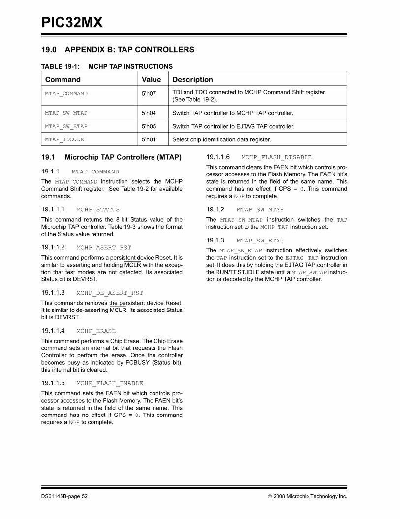
PIC32MX
19.0 APPENDIX B: TAP CONTROLLERS
TABLE 19-1: MCHP TAP INSTRUCTIONS
19.1 Microchip TAP Controllers (MTAP)
19.1.1 MTAP_COMMAND
The MTAP_COMMAND instruction selects the MCHPCommand Shift register. See Table 19-2 for availablecommands.
19.1.1.1 MCHP_STATUS
This command returns the 8-bit Status value of theMicrochip TAP controller. Table 19-3 shows the formatof the Status value returned.
19.1.1.2 MCHP_ASERT_RST This command performs a persistent device Reset. It issimilar to asserting and holding MCLR with the excep-tion that test modes are not detected. Its associatedStatus bit is DEVRST.
19.1.1.3 MCHP_DE_ASERT_RST
This commands removes the persistent device Reset.It is similar to de-asserting MCLR. Its associated Statusbit is DEVRST.
19.1.1.4 MCHP_ERASE
This command performs a Chip Erase. The Chip Erasecommand sets an internal bit that requests the FlashController to perform the erase. Once the controllerbecomes busy as indicated by FCBUSY (Status bit),this internal bit is cleared.
19.1.1.5 MCHP_FLASH_ENABLE
This command sets the FAEN bit which controls pro-cessor accesses to the Flash Memory. The FAEN bit’sstate is returned in the field of the same name. Thiscommand has no effect if CPS = 0. This commandrequires a NOP to complete.
19.1.1.6 MCHP_FLASH_DISABLE
This command clears the FAEN bit which controls pro-cessor accesses to the Flash Memory. The FAEN bit’sstate is returned in the field of the same name. Thiscommand has no effect if CPS = 0. This commandrequires a NOP to complete.
19.1.2 MTAP_SW_MTAP
The MTAP_SW_MTAP instruction switches the TAPinstruction set to the MCHP TAP instruction set.
19.1.3 MTAP_SW_ETAP The MTAP_SW_ETAP instruction effectively switchesthe TAP instruction set to the EJTAG TAP instructionset. It does this by holding the EJTAG TAP controller inthe RUN/TEST/IDLE state until a MTAP_SWTAP instruc-tion is decoded by the MCHP TAP controller.
Command Value Description
MTAP_COMMAND 5’h07 TDI and TDO connected to MCHP Command Shift register (See Table 19-2).
MTAP_SW_MTAP 5’h04 Switch TAP controller to MCHP TAP controller.
MTAP_SW_ETAP 5’h05 Switch TAP controller to EJTAG TAP controller.
MTAP_IDCODE 5’h01 Select chip identification data register.
DS61145B-page 52 © 2008 Microchip Technology Inc.

PIC32MX
TABLE 19-2: MTAP_COMMAND DR COMMANDSTABLE 19-3: MCHP STATUS VALUE.
TABLE 19-4: EJTAG TAP INSTRUCTIONS
Command Value Description
MCHP_STATUS 8’h00 NOP and return Status
MCHP_ASERT_RST 8’hD1 Requests the reset controller to assert device Reset
MCHP_DE_ASERT_RST 8’hD0 Removes the request for device Reset which causes the reset controller to de-assert device Reset if there is no other source requesting Reset (i.e. MCLR)
MCHP_ERASE 8’hFC Cause the Flash controller to perform a Chip Erase
MCHP_FLASH_ENABLE 8’hFE Enables fetches and loads to the Flash (from the processor)
MCHP_FLASH_DISABLE 8’hFD Disables fetches and loads to the Flash (from the processor)
CPS 0 0 0 CFGRDY FCBUSY FAEN DEVRSTbit 7 bit 0
bit 7 CPS: Code-Protect State bit0 = Device is code-protected1 = Device is NOT code-protected
bit 6 Unimplemented: Read as ‘0’bit 5-4 Unimplemented: Read as ‘0’bit 3 CFGRDY: Code-Protect State bit
0 = Configuration has not been read1 = Configuration has been read and CP is valid
bit 2 FCBUSY: Flash Controller Busy bit0 = Flash Controller is Not Busy (Either erase has not started or it has finished)1 = Flash Controller is Busy (Erase is in progress)
bit 1 FAEN: Flash Access Enable bitThis bit reflects the state of CFGCON.FAEN.0 = Flash access is disabled (i.e., processor accesses are blocked)1 = Flash access is enabled
bit 0 DEVRST: Device Reset State bit0 = Device Reset is NOT active1 = Device Reset is active
Command Value Description
ETAP_ADDRESS 5’h08 Select Address register
ETAP_DATA 5’h09 Select Data register
ETAP_CONTROL 5’h0A Select EJTAG Control register
ETAP_EJTAGBOOT 5’h0C Set EjtagBrk, ProbEn and ProbTrap to 1 as Reset value
ETAP_FASTDATA 5’h0E Selects the Data and Fastdata registers
© 2008 Microchip Technology Inc. DS61145B-page 53

PIC32MX
19.2 EJTAG TAP Controller19.2.1 ETAP_ADDRESS
This command selects the address register. Theread-only address register provides the address for aprocessor access. The value read in the register isvalid if a processor access is pending, otherwise thevalue is undefined.
The two or three LSBs of the register are used with thePsz field from the EJTAG Control register to indicatethe size and data position of the pending processoraccess transfer. These bits are not taken directly fromthe address referenced by the load/store.
19.2.2 ETAP_DATA
This command selects the data register. The read/writedata register is used for opcode and data transfers dur-ing processor accesses. The value read in the dataregister is valid only if a processor access for a write ispending, in which case the data register holds the storevalue. The value written to the data register is only usedif a processor access for a pending read is finishedafterwards, in which case the data value written is thevalue for the fetch or load. This behavior implies thatthe data register is not a memory location where apreviously written value can be read afterwards.
19.2.3 ETAP_CONTROL
This command selects the control register. The EJTAGControl Register (ECR) handles processor Reset andsoft Reset indication, Debug mode indication, accessstart, finish, and size and read/write indication. TheECR also:
• controls debug vector location and indication of serviced processor accesses,
• allows a debug interrupt request,• indicates processor Low-Power mode, and• allows implementation-dependent processor and
peripheral Resets.
The EJTAG Control register is not updated/written inthe Update-DR state unless the Reset occurred; that isRocc (bit 31) is either already ‘0’ or is written to ‘0’ atthe same time. This condition ensures proper handlingof processor accesses after a Reset.
Reset of the processor can be indicated through theRocc bit in the TCK domain a number of TCK cyclesafter it is removed in the processor clock domain inorder to allow for proper synchronization between thetwo clock domains.
Bits that are R/W in the register return their writtenvalue on a subsequent read, unless other behavior isdefined.
Internal synchronization ensures that a written value isupdated for reading immediately afterwards, evenwhen the TAP controller takes the shortest path fromthe Update-DR to Capture-DR state.
19.2.4 ETAP_EJTAGBOOT
The Reset value of the EjtagBrk, ProbTrap, andProbEn bits follows the setting of the internal EJTAG-BOOT indication.
If the EJTAGBOOT instruction has been given, and theinternal EJTAGBOOT indication is active, then theReset value of the three bits is set (1), otherwise theReset value is clear (0).
The results of setting these bits are:
• Setting the EjtagBrk causes a Debug interrupt exception to be requested right after the proces-sor Reset from the EJTAGBOOT instruction
• The debug handler is executed from the EJTAG memory because ProbTrap is set to indicate debug vector in EJTAG memory at 0x FF20 0200
• Service of the processor access is indicated because ProbEn is set
Thus it is possible to execute the debug handler rightafter a processor Reset from the EJTAGBOOT instruc-tion, without executing any instructions from the normalReset handler.
19.2.5 ETAP_FASTDATA
The width of the Fastdata register is 1 bit. During aFastdata access, the Fastdata register is written andread (i.e., a bit is shifted in and a bit is shifted out). Dur-ing a Fastdata access, the Fastdata register valueshifted in specifies whether the Fastdata access shouldbe completed or not. The value shifted out is a flag thatindicates whether the Fastdata access was successfulor not (if completion was requested). The FASTDATAaccess is used for efficient block transfers between theDMSEG segment (on the probe) and target memory(on the processor). An “upload” is defined as asequence of processor loads from target memory andstores to the DMSEG segment. A “download” is asequence of processor loads from the DMSEG seg-ment and stores to target memory. The “Fastdata area”specifies the legal range of DMSEG segmentaddresses (0xFF20.0000-0xFF20.000F) that can beused for uploads and downloads. The Data and Fast-data registers (selected with the FASTDATA instruction)allow efficient completion of pending Fastdata areaaccesses.
During Fastdata uploads and downloads, the proces-sor will stall on accesses to the Fastdata area. ThePrAcc (processor access pending bit) will be 1 indicat-ing the probe is required to complete the access. Bothupload and download accesses are attempted by shift-ing in a zero SPrAcc value (to request access comple-tion) and shifting out SPrAcc to see if the attempt will besuccessful (i.e., there was an access pending and alegal Fastdata area address was used).
DS61145B-page 54 © 2008 Microchip Technology Inc.

PIC32MX
Downloads will also shift in the data to be used to sat-isfy the load from the DMSEG segment Fastdata area,while uploads will shift out the data being stored to theDMSEG segment Fastdata area.As noted above, two conditions must be true for theFastdata access to succeed. These are:
• PrAcc must be 1 (i.e., there must be a pending processor access).
• The Fastdata operation must use a valid Fastdata area address in the DMSEG segment (0xFF20.0000 to 0xFF20.000F).
© 2008 Microchip Technology Inc. DS61145B-page 55

PIC32MX
20.0 APPENDIX C: AC/DC CHARACTERISTICS AND TIMING REQUIREMENTSTABLE 20-1: AC/DC CHARACTERISTICS AND TIMING REQUIREMENTS
Standard Operating ConditionsOperating Temperature: 0°C to +70°C. Programming at +25°C is recommended.
Param No. Symbol Characteristic Min. Max. Units Conditions
D111 VDD Supply Voltage During Programming 3.0V 3.60 V Normal programming(1,2)
D112 IPP Programming Current on MCLR — 5 μAD113 IDDP Supply Current During Programming — 40 mAD031 VIL Input Low Voltage VSS 0.2 VDD VD041 VIH Input High Voltage 0.8 VDD VDD VD080 VOL Output Low Voltage — 0.4 V IOL = 8.5 mA @ 3.6VD090 VOH Output High Voltage 1.4 — V IOH = -3.0 mA @ 3.6VD012 CIO Capacitive Loading on I/O pin (PGDx) — 50 pF To meet AC specificationsD013 CF Filter Capacitor Value on VCAP 1 10 μF Required for controller coreP1 TPGC Serial Clock (PGCx) Period 100 — nsP1A TPGCL Serial Clock (PGCx) Low Time 40 — nsP1B TPGCH Serial Clock (PGCx) High Time 40 — nsP2 TSET1 Input Data Setup Time to Serial Clock ↓ 15 — nsP3 THLD1 Input Data Hold Time from PGCx ↓ 15 — nsP4 TDLY1 Delay between 4-bit Command and
Command Operand40 — ns
P4A TDLY1A Delay between 4-bit Command Operand and Next 4-bit Command
40 — ns
P5 TDLY2 Delay between Last PGCx ↓ of Command Byte to First PGCx ↑ of Read of Data Word
20 — ns
P6 TSET2 VDD ↑ Setup Time to MCLR ↑ 100 — ns
P7 THLD2 Input Data Hold Time from MCLR ↑ 500 — nsP8 TDLY3 Delay between Last PGCx ↓ of Command
Byte to PGDx ↑ by Programming Executive20 — μs
P9A TDLY4 Programming Executive Command Processing Time
40 — μs
P9B TDLY5 Delay between PGDx ↓ by Programming Executive to PGDx Released by Programming Executive
15 — μs
P10 TDLY6 PGCx Low Time After Programming 400 — nsP11 TDLY7 Chip Erase Time 400 — msP12 TDLY8 Page Erase Time 40 — msP13 TDLY9 Row Programming Time 2 — ms
P14 TR MCLR Rise Time to Enter ICSP™ mode — 1.0 μsP15 TVALID Data Out Valid from PGCx ↑ 10 — ns
P16 TDLY8 Delay between Last PGCx ↓ and MCLR ↓ 0 — s
P17 THLD3 MCLR ↓ to VDD ↓ — 100 ns
P18 TKEY1 Delay from First MCLR ↓ to First PGCx ↑ for Key Sequence on PGDx
40 — ns
Note 1: VDDCORE must be supplied to the VDDCORE/VCAP pin if the on-chip voltage regulator is disabled. See Section 4.3 “Power Requirements” for more information.
2: VDD must also be supplied to the AVDD pins during programming. AVDD and AVSS should always be within ±0.3V of VDD and VSS, respectively.
DS61145B-page 56 © 2008 Microchip Technology Inc.

PIC32MX
P19 TKEY2 Delay from Last PGCx ↓ for Key Sequence on PGDx to Second MCLR ↑
40 — ns
TABLE 20-1: AC/DC CHARACTERISTICS AND TIMING REQUIREMENTS (CONTINUED)
Standard Operating ConditionsOperating Temperature: 0°C to +70°C. Programming at +25°C is recommended.
Param No. Symbol Characteristic Min. Max. Units Conditions
Note 1: VDDCORE must be supplied to the VDDCORE/VCAP pin if the on-chip voltage regulator is disabled. See Section 4.3 “Power Requirements” for more information.
2: VDD must also be supplied to the AVDD pins during programming. AVDD and AVSS should always be within ±0.3V of VDD and VSS, respectively.
© 2008 Microchip Technology Inc. DS61145B-page 57

PIC32MX
21.0 APPENDIX D: PIC32MX FLASH MEMORY MAP
FIGURE 21-1: FLASH MEMORY MAP
Boot Page 0
Boot Page 1
Boot Page 2Debug Page
Configuration Words(4 x 32 bits)
1FO00000h
1FO01FFFh
1FO02FF0h
1FO02FFFh
1DO00000h
Program Flash Memory
1DO07FFFh
PFM
BFM
DS61145B-page 58 © 2008 Microchip Technology Inc.

Note the following details of the code protection feature on Microchip devices:• Microchip products meet the specification contained in their particular Microchip Data Sheet.
• Microchip believes that its family of products is one of the most secure families of its kind on the market today, when used in the intended manner and under normal conditions.
• There are dishonest and possibly illegal methods used to breach the code protection feature. All of these methods, to our knowledge, require using the Microchip products in a manner outside the operating specifications contained in Microchip’s Data Sheets. Most likely, the person doing so is engaged in theft of intellectual property.
• Microchip is willing to work with the customer who is concerned about the integrity of their code.
• Neither Microchip nor any other semiconductor manufacturer can guarantee the security of their code. Code protection does not mean that we are guaranteeing the product as “unbreakable.”
Code protection is constantly evolving. We at Microchip are committed to continuously improving the code protection features of ourproducts. Attempts to break Microchip’s code protection feature may be a violation of the Digital Millennium Copyright Act. If such actsallow unauthorized access to your software or other copyrighted work, you may have a right to sue for relief under that Act.
Information contained in this publication regarding deviceapplications and the like is provided only for your convenienceand may be superseded by updates. It is your responsibility toensure that your application meets with your specifications.MICROCHIP MAKES NO REPRESENTATIONS ORWARRANTIES OF ANY KIND WHETHER EXPRESS ORIMPLIED, WRITTEN OR ORAL, STATUTORY OROTHERWISE, RELATED TO THE INFORMATION,INCLUDING BUT NOT LIMITED TO ITS CONDITION,QUALITY, PERFORMANCE, MERCHANTABILITY ORFITNESS FOR PURPOSE. Microchip disclaims all liabilityarising from this information and its use. Use of Microchipdevices in life support and/or safety applications is entirely atthe buyer’s risk, and the buyer agrees to defend, indemnify andhold harmless Microchip from any and all damages, claims,suits, or expenses resulting from such use. No licenses areconveyed, implicitly or otherwise, under any Microchipintellectual property rights.
© 2008 Microchip Technology Inc.
Trademarks
The Microchip name and logo, the Microchip logo, Accuron, dsPIC, KEELOQ, KEELOQ logo, MPLAB, PIC, PICmicro, PICSTART, PRO MATE, rfPIC and SmartShunt are registered trademarks of Microchip Technology Incorporated in the U.S.A. and other countries.
FilterLab, Linear Active Thermistor, MXDEV, MXLAB, SEEVAL, SmartSensor and The Embedded Control Solutions Company are registered trademarks of Microchip Technology Incorporated in the U.S.A.
Analog-for-the-Digital Age, Application Maestro, CodeGuard, dsPICDEM, dsPICDEM.net, dsPICworks, dsSPEAK, ECAN, ECONOMONITOR, FanSense, In-Circuit Serial Programming, ICSP, ICEPIC, Mindi, MiWi, MPASM, MPLAB Certified logo, MPLIB, MPLINK, mTouch, PICkit, PICDEM, PICDEM.net, PICtail, PIC32 logo, PowerCal, PowerInfo, PowerMate, PowerTool, REAL ICE, rfLAB, Select Mode, Total Endurance, UNI/O, WiperLock and ZENA are trademarks of Microchip Technology Incorporated in the U.S.A. and other countries.
SQTP is a service mark of Microchip Technology Incorporated in the U.S.A.
All other trademarks mentioned herein are property of their respective companies.
© 2008, Microchip Technology Incorporated, Printed in the U.S.A., All Rights Reserved.
Printed on recycled paper.
DS61145B-page 55
Microchip received ISO/TS-16949:2002 certification for its worldwide headquarters, design and wafer fabrication facilities in Chandler and Tempe, Arizona; Gresham, Oregon and design centers in California and India. The Company’s quality system processes and procedures are for its PIC® MCUs and dsPIC® DSCs, KEELOQ® code hopping devices, Serial EEPROMs, microperipherals, nonvolatile memory and analog products. In addition, Microchip’s quality system for the design and manufacture of development systems is ISO 9001:2000 certified.

DS61145B-page 56 © 2008 Microchip Technology Inc.
AMERICASCorporate Office2355 West Chandler Blvd.Chandler, AZ 85224-6199Tel: 480-792-7200 Fax: 480-792-7277Technical Support: http://support.microchip.comWeb Address: www.microchip.comAtlantaDuluth, GA Tel: 678-957-9614 Fax: 678-957-1455BostonWestborough, MA Tel: 774-760-0087 Fax: 774-760-0088ChicagoItasca, IL Tel: 630-285-0071 Fax: 630-285-0075DallasAddison, TX Tel: 972-818-7423 Fax: 972-818-2924DetroitFarmington Hills, MI Tel: 248-538-2250Fax: 248-538-2260KokomoKokomo, IN Tel: 765-864-8360Fax: 765-864-8387Los AngelesMission Viejo, CA Tel: 949-462-9523 Fax: 949-462-9608Santa ClaraSanta Clara, CA Tel: 408-961-6444Fax: 408-961-6445TorontoMississauga, Ontario, CanadaTel: 905-673-0699 Fax: 905-673-6509
ASIA/PACIFICAsia Pacific OfficeSuites 3707-14, 37th FloorTower 6, The GatewayHarbour City, KowloonHong KongTel: 852-2401-1200Fax: 852-2401-3431Australia - SydneyTel: 61-2-9868-6733Fax: 61-2-9868-6755China - BeijingTel: 86-10-8528-2100 Fax: 86-10-8528-2104China - ChengduTel: 86-28-8665-5511Fax: 86-28-8665-7889China - Hong Kong SARTel: 852-2401-1200 Fax: 852-2401-3431China - NanjingTel: 86-25-8473-2460Fax: 86-25-8473-2470China - QingdaoTel: 86-532-8502-7355Fax: 86-532-8502-7205China - ShanghaiTel: 86-21-5407-5533 Fax: 86-21-5407-5066China - ShenyangTel: 86-24-2334-2829Fax: 86-24-2334-2393China - ShenzhenTel: 86-755-8203-2660 Fax: 86-755-8203-1760China - WuhanTel: 86-27-5980-5300Fax: 86-27-5980-5118China - XiamenTel: 86-592-2388138 Fax: 86-592-2388130China - XianTel: 86-29-8833-7252Fax: 86-29-8833-7256China - ZhuhaiTel: 86-756-3210040 Fax: 86-756-3210049
ASIA/PACIFICIndia - BangaloreTel: 91-80-4182-8400 Fax: 91-80-4182-8422India - New DelhiTel: 91-11-4160-8631Fax: 91-11-4160-8632India - PuneTel: 91-20-2566-1512Fax: 91-20-2566-1513Japan - YokohamaTel: 81-45-471- 6166 Fax: 81-45-471-6122Korea - DaeguTel: 82-53-744-4301Fax: 82-53-744-4302Korea - SeoulTel: 82-2-554-7200Fax: 82-2-558-5932 or 82-2-558-5934Malaysia - Kuala LumpurTel: 60-3-6201-9857Fax: 60-3-6201-9859Malaysia - PenangTel: 60-4-227-8870Fax: 60-4-227-4068Philippines - ManilaTel: 63-2-634-9065Fax: 63-2-634-9069SingaporeTel: 65-6334-8870Fax: 65-6334-8850Taiwan - Hsin ChuTel: 886-3-572-9526Fax: 886-3-572-6459Taiwan - KaohsiungTel: 886-7-536-4818Fax: 886-7-536-4803Taiwan - TaipeiTel: 886-2-2500-6610 Fax: 886-2-2508-0102Thailand - BangkokTel: 66-2-694-1351Fax: 66-2-694-1350
EUROPEAustria - WelsTel: 43-7242-2244-39Fax: 43-7242-2244-393Denmark - CopenhagenTel: 45-4450-2828 Fax: 45-4485-2829France - ParisTel: 33-1-69-53-63-20 Fax: 33-1-69-30-90-79Germany - MunichTel: 49-89-627-144-0 Fax: 49-89-627-144-44Italy - Milan Tel: 39-0331-742611 Fax: 39-0331-466781Netherlands - DrunenTel: 31-416-690399 Fax: 31-416-690340Spain - MadridTel: 34-91-708-08-90Fax: 34-91-708-08-91UK - WokinghamTel: 44-118-921-5869Fax: 44-118-921-5820
WORLDWIDE SALES AND SERVICE
01/02/08