Embed Size (px)
Citation preview
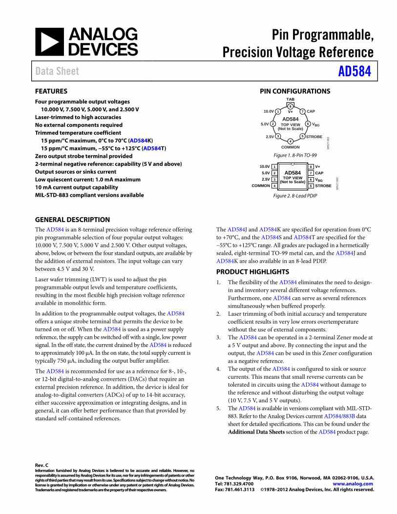
Pin Programmable, Precision Voltage Reference
Data Sheet AD584
Rev. C Information furnished by Analog Devices is believed to be accurate and reliable. However, no responsibility is assumed by Analog Devices for its use, nor for any infringements of patents or other rights of third parties that may result from its use. Specifications subject to change without notice. No license is granted by implication or otherwise under any patent or patent rights of Analog Devices. Trademarks and registered trademarks are the property of their respective owners.
One Technology Way, P.O. Box 9106, Norwood, MA 02062-9106, U.S.A. Tel: 781.329.4700 www.analog.com Fax: 781.461.3113 ©1978–2012 Analog Devices, Inc. All rights reserved.
FEATURES Four programmable output voltages
10.000 V, 7.500 V, 5.000 V, and 2.500 V Laser-trimmed to high accuracies No external components required Trimmed temperature coefficient
15 ppm/°C maximum, 0°C to 70°C (AD584K) 15 ppm/°C maximum, −55°C to +125°C (AD584T)
Zero output strobe terminal provided 2-terminal negative reference: capability (5 V and above) Output sources or sinks current Low quiescent current: 1.0 mA maximum 10 mA current output capability MIL-STD-883 compliant versions available
PIN CONFIGURATIONS
Figure 1. 8-Pin TO-99
Figure 2. 8-Lead PDIP
GENERAL DESCRIPTION The AD584 is an 8-terminal precision voltage reference offering pin programmable selection of four popular output voltages: 10.000 V, 7.500 V, 5.000 V and 2.500 V. Other output voltages, above, below, or between the four standard outputs, are available by the addition of external resistors. The input voltage can vary between 4.5 V and 30 V.
Laser wafer trimming (LWT) is used to adjust the pin programmable output levels and temperature coefficients, resulting in the most flexible high precision voltage reference available in monolithic form.
In addition to the programmable output voltages, the AD584 offers a unique strobe terminal that permits the device to be turned on or off. When the AD584 is used as a power supply reference, the supply can be switched off with a single, low power signal. In the off state, the current drained by the AD584 is reduced to approximately 100 µA. In the on state, the total supply current is typically 750 µA, including the output buffer amplifier.
The AD584 is recommended for use as a reference for 8-, 10-, or 12-bit digital-to-analog converters (DACs) that require an external precision reference. In addition, the device is ideal for analog-to-digital converters (ADCs) of up to 14-bit accuracy, either successive approximation or integrating designs, and in general, it can offer better performance than that provided by standard self-contained references.
The AD584J and AD584K are specified for operation from 0°C to +70°C, and the AD584S and AD584T are specified for the −55°C to +125°C range. All grades are packaged in a hermetically sealed, eight-terminal TO-99 metal can, and the AD584J and AD584K are also available in an 8-lead PDIP.
PRODUCT HIGHLIGHTS 1. The flexibility of the AD584 eliminates the need to design-
in and inventory several different voltage references. Furthermore, one AD584 can serve as several references simultaneously when buffered properly.
2. Laser trimming of both initial accuracy and temperature coefficient results in very low errors overtemperature without the use of external components.
3. The AD584 can be operated in a 2-terminal Zener mode at a 5 V output and above. By connecting the input and the output, the AD584 can be used in this Zener configuration as a negative reference.
4. The output of the AD584 is configured to sink or source currents. This means that small reverse currents can be tolerated in circuits using the AD584 without damage to the reference and without disturbing the output voltage (10 V, 7.5 V, and 5 V outputs).
5. The AD584 is available in versions compliant with MIL-STD-883. Refer to the Analog Devices current AD584/883B data sheet for detailed specifications. This can be found under the Additional Data Sheets section of the AD584 product page.
1
2 6
7
3 5
8V+
TAB
4
AD584TOP VIEW
(Not to Scale)
COMMON
STROBE
VBG
CAP
2.5V
5.0V
10.0V
0052
7-00
1
10.0V 1
5.0V 2
2.5V 3
COMMON 4
V+8
CAP7
VBG6
STROBE5
AD584TOP VIEW
(Not to Scale)
0052
7-00
2
AD584 Data Sheet
Rev. C | Page 2 of 12
TABLE OF CONTENTS Features .............................................................................................. 1 Pin Configurations ........................................................................... 1 General Description ......................................................................... 1 Product Highlights ........................................................................... 1 Revision History ............................................................................... 2 Specifications ..................................................................................... 3 Absolute Maximum Ratings ............................................................ 5
ESD Caution .................................................................................. 5 Theory of Operation ........................................................................ 6
Applying the AD584 .................................................................... 6 Performance over Temperature .................................................. 7
Output Current Characteristics ...................................................7 Dynamic Performance ..................................................................7 Noise Filtering ...............................................................................8 Using the Strobe Terminal ...........................................................8 Percision High Current Supply....................................................8 The AD584 as a Current Limiter.................................................9 Negative Reference Voltages from an AD584 ...............................9 10 V Reference with Multiplying CMOS DACs or ADCs .......9 Precision DAC Reference .......................................................... 10
Outline Dimensions ....................................................................... 11 Ordering Guide .......................................................................... 12
REVISION HISTORY 5/12—Rev. B to Rev. C Deleted AD584L ................................................................. Universal Changes to Features Section, General Description Section and Product Highlights Section ............................................................. 1 Deleted Metalization Photograph .................................................. 4 Changes to 10 V Reference with Multiplying CMOS DACs or ADCs Section .................................................................................... 9 Changes to Precision DAC Reference Section and Figure 19... 10 Updated Outline Dimensions ....................................................... 11 Changes to Ordering Guide .......................................................... 12 7/01—Rev. A to Rev. B

Data Sheet AD584
Rev. C | Page 3 of 12
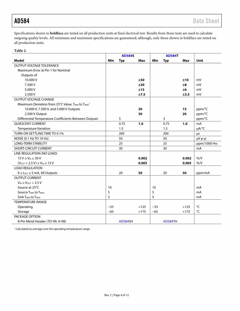
SPECIFICATIONS VIN = 15 V and 25°C, unless otherwise noted.
Specifications shown in boldface are tested on all production units at final electrical test. Results from those tests are used to calculate outgoing quality levels. All minimum and maximum specifications are guaranteed; although, only those shown in boldface are tested on all production units.
Table 1. AD584J AD584K Model Min Typ Max Min Typ Max Unit OUTPUT VOLTAGE TOLERANCE
Maximum Error at Pin 1 for Nominal Outputs of
10.000 V ±30 ±10 mV 7.500 V ±20 ±8 mV 5.000 V ±15 ±6 mV 2.500 V ±7.5 ±3.5 mV
OUTPUT VOLTAGE CHANGE Maximum Deviation from 25°C Value, TMIN to TMAX
1 10.000 V, 7.500 V, and 5.000 V Outputs 30 15 ppm/°C 2.500 V Output 30 15 ppm/°C
Differential Temperature Coefficients Between Outputs 5 3 ppm/°C QUIESCENT CURRENT 0.75 1.0 0.75 1.0 mA
Temperature Variation 1.5 1.5 µA/°C TURN-ON SETTLING TIME TO 0.1% 200 200 µs NOISE (0.1 Hz TO 10 Hz) 50 50 µV p-p LONG-TERM STABILITY 25 25 ppm/1000 Hrs SHORT-CIRCUIT CURRENT 30 30 mA LINE REGULATION (NO LOAD)
15 V ≤ VIN ≤ 30 V 0.002 0.002 %/V (VOUT + 2.5 V) ≤ VIN ≤ 15 V 0.005 0.005 %/V
LOAD REGULATION 0 ≤ IOUT ≤ 5 mA, All Outputs 20 50 20 50 ppm/mA
OUTPUT CURRENT VIN ≥ VOUT + 2.5 V
Source at 25°C 10 10 mA Source TMIN to TMAX 5 5 mA Sink TMIN to TMAX 5 5 mA
TEMPERATURE RANGE Operating 0 70 0 70 °C Storage −65 +175 −65 +175 °C
PACKAGE OPTION 8-Pin Metal Header (TO-99, H-08) AD584JH AD584KH 8-Lead Plastic Dual In-Line Package (PDIP, N-8) AD584JN AD584KN
1 Calculated as average over the operating temperature range.
AD584 Data Sheet
Rev. C | Page 4 of 12
Specifications shown in boldface are tested on all production units at final electrical test. Results from those tests are used to calculate outgoing quality levels. All minimum and maximum specifications are guaranteed; although, only those shown in boldface are tested on all production units.
Table 2. AD584S AD584T Model Min Typ Max Min Typ Max Unit OUTPUT VOLTAGE TOLERANCE
Maximum Error at Pin 1 for Nominal Outputs of
10.000 V ±30 ±10 mV 7.500 V ±20 ±8 mV 5.000 V ±15 ±6 mV 2.500 V ±7.5 ±3.5 mV
OUTPUT VOLTAGE CHANGE Maximum Deviation from 25°C Value, TMIN to TMAX
1 10.000 V, 7.500 V, and 5.000 V Outputs 30 15 ppm/°C 2.500 V Output 30 20 ppm/°C
Differential Temperature Coefficients Between Outputs 5 3 ppm/°C QUIESCENT CURRENT 0.75 1.0 0.75 1.0 mA
Temperature Variation 1.5 1.5 µA/°C TURN-ON SETTLING TIME TO 0.1% 200 200 µs NOISE (0.1 Hz TO 10 Hz) 50 50 µV p-p LONG-TERM STABILITY 25 25 ppm/1000 Hrs SHORT-CIRCUIT CURRENT 30 30 mA LINE REGULATION (NO LOAD)
15 V ≤ VIN ≤ 30 V 0.002 0.002 %/V (VOUT + 2.5 V) ≤ VIN ≤ 15 V 0.005 0.005 %/V
LOAD REGULATION 0 ≤ IOUT ≤ 5 mA, All Outputs 20 50 20 50 ppm/mA
OUTPUT CURRENT VIN ≥ VOUT + 2.5 V Source at 25°C 10 10 mA Source TMIN to TMAX 5 5 mA Sink TMIN to TMAX 5 5 mA
TEMPERATURE RANGE Operating −55 +125 −55 +125 °C Storage −65 +175 −65 +175 °C
PACKAGE OPTION 8-Pin Metal Header (TO-99, H-08) AD584SH AD584TH
1 Calculated as average over the operating temperature range.
Data Sheet AD584
Rev. C | Page 5 of 12
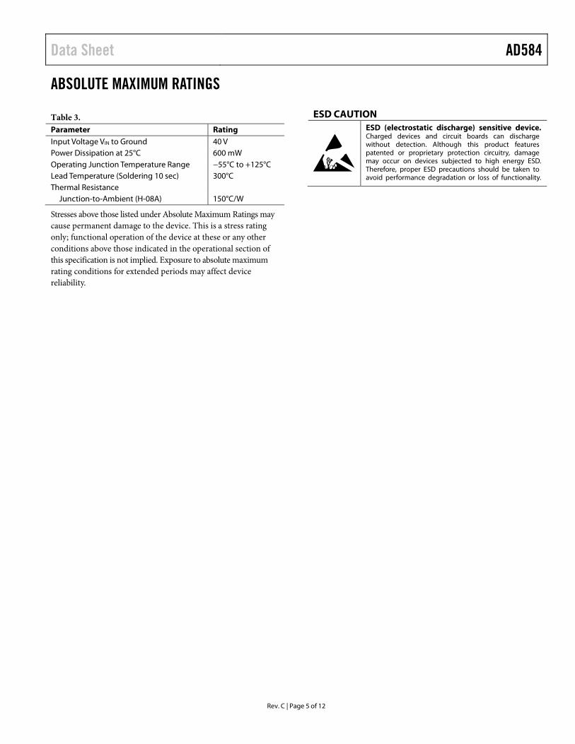
ABSOLUTE MAXIMUM RATINGS
Table 3. Parameter Rating Input Voltage VIN to Ground 40 V Power Dissipation at 25°C 600 mW Operating Junction Temperature Range −55°C to +125°C Lead Temperature (Soldering 10 sec) 300°C Thermal Resistance
Junction-to-Ambient (H-08A) 150°C/W
Stresses above those listed under Absolute Maximum Ratings may cause permanent damage to the device. This is a stress rating only; functional operation of the device at these or any other conditions above those indicated in the operational section of this specification is not implied. Exposure to absolute maximum rating conditions for extended periods may affect device reliability.
ESD CAUTION
AD584 Data Sheet
Rev. C | Page 6 of 12
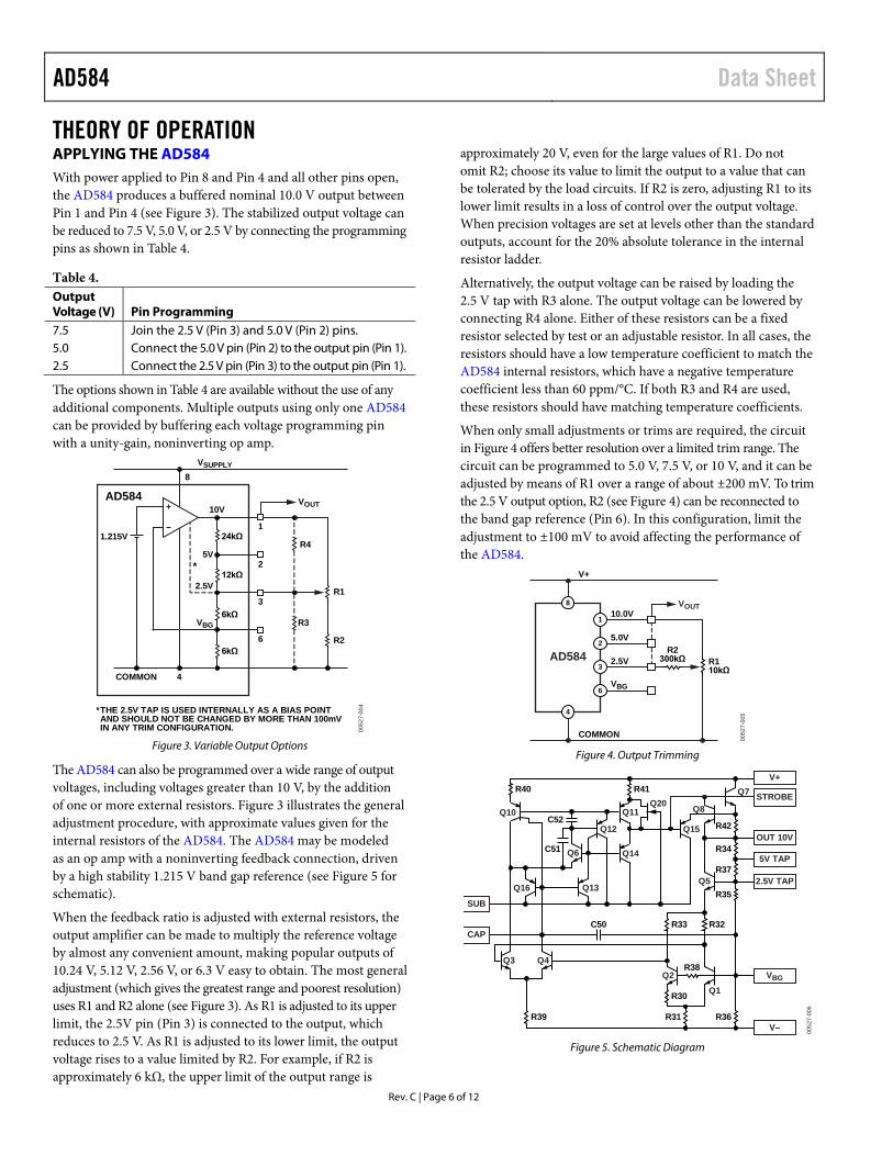
THEORY OF OPERATION APPLYING THE AD584 With power applied to Pin 8 and Pin 4 and all other pins open, the AD584 produces a buffered nominal 10.0 V output between Pin 1 and Pin 4 (see Figure 3). The stabilized output voltage can be reduced to 7.5 V, 5.0 V, or 2.5 V by connecting the programming pins as shown in Table 4.
Table 4. Output Voltage (V) Pin Programming 7.5 Join the 2.5 V (Pin 3) and 5.0 V (Pin 2) pins. 5.0 Connect the 5.0 V pin (Pin 2) to the output pin (Pin 1). 2.5 Connect the 2.5 V pin (Pin 3) to the output pin (Pin 1).
The options shown in Table 4 are available without the use of any additional components. Multiple outputs using only one AD584 can be provided by buffering each voltage programming pin with a unity-gain, noninverting op amp.
Figure 3. Variable Output Options
The AD584 can also be programmed over a wide range of output voltages, including voltages greater than 10 V, by the addition of one or more external resistors. Figure 3 illustrates the general adjustment procedure, with approximate values given for the internal resistors of the AD584. The AD584 may be modeled as an op amp with a noninverting feedback connection, driven by a high stability 1.215 V band gap reference (see Figure 5 for schematic).
When the feedback ratio is adjusted with external resistors, the output amplifier can be made to multiply the reference voltage by almost any convenient amount, making popular outputs of 10.24 V, 5.12 V, 2.56 V, or 6.3 V easy to obtain. The most general adjustment (which gives the greatest range and poorest resolution) uses R1 and R2 alone (see Figure 3). As R1 is adjusted to its upper limit, the 2.5V pin (Pin 3) is connected to the output, which reduces to 2.5 V. As R1 is adjusted to its lower limit, the output voltage rises to a value limited by R2. For example, if R2 is approximately 6 kΩ, the upper limit of the output range is
approximately 20 V, even for the large values of R1. Do not omit R2; choose its value to limit the output to a value that can be tolerated by the load circuits. If R2 is zero, adjusting R1 to its lower limit results in a loss of control over the output voltage. When precision voltages are set at levels other than the standard outputs, account for the 20% absolute tolerance in the internal resistor ladder.
Alternatively, the output voltage can be raised by loading the 2.5 V tap with R3 alone. The output voltage can be lowered by connecting R4 alone. Either of these resistors can be a fixed resistor selected by test or an adjustable resistor. In all cases, the resistors should have a low temperature coefficient to match the AD584 internal resistors, which have a negative temperature coefficient less than 60 ppm/°C. If both R3 and R4 are used, these resistors should have matching temperature coefficients.
When only small adjustments or trims are required, the circuit in Figure 4 offers better resolution over a limited trim range. The circuit can be programmed to 5.0 V, 7.5 V, or 10 V, and it can be adjusted by means of R1 over a range of about ±200 mV. To trim the 2.5 V output option, R2 (see Figure 4) can be reconnected to the band gap reference (Pin 6). In this configuration, limit the adjustment to ±100 mV to avoid affecting the performance of the AD584.
Figure 4. Output Trimming
Figure 5. Schematic Diagram
AD584
VSUPPLY
VOUT
8
1
2
3
6
1.215V
10V
5V*
2.5V12kΩ
6kΩVBG
R4
4COMMON
R1
R2
R3
6kΩ
24kΩ
*THE 2.5V TAP IS USED INTERNALLY AS A BIAS POINTAND SHOULD NOT BE CHANGED BY MORE THAN 100mVIN ANY TRIM CONFIGURATION. 00
527-
004
AD584
VOUT
110.0V
8
V+
4
COMMON
25.0V
32.5V
6VBG
R110kΩ
R2300kΩ
0052
7-00
5
R38
R40
Q10
Q16 Q13
Q11
Q14
Q12 Q15
SUB
CAP
R41
R42
R34
R37
R35
R30
R31 R36
Q6
Q8
Q5
C51
C52
C50
Q20Q7 STROBE
V+
OUT 10V
5V TAP
2.5V TAP
VBG
V–
R32R33
Q3 Q4Q2
Q1
R39
0052
7-00
6
Data Sheet AD584
Rev. C | Page 7 of 12
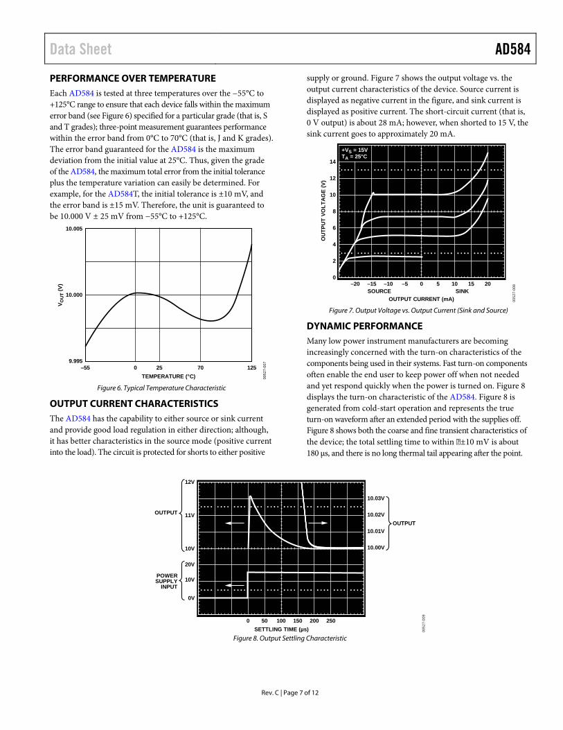
PERFORMANCE OVER TEMPERATURE Each AD584 is tested at three temperatures over the −55°C to +125°C range to ensure that each device falls within the maximum error band (see Figure 6) specified for a particular grade (that is, S and T grades); three-point measurement guarantees performance within the error band from 0°C to 70°C (that is, J and K grades). The error band guaranteed for the AD584 is the maximum deviation from the initial value at 25°C. Thus, given the grade of the AD584, the maximum total error from the initial tolerance plus the temperature variation can easily be determined. For example, for the AD584T, the initial tolerance is ±10 mV, and the error band is ±15 mV. Therefore, the unit is guaranteed to be 10.000 V ± 25 mV from −55°C to +125°C.
Figure 6. Typical Temperature Characteristic
OUTPUT CURRENT CHARACTERISTICS The AD584 has the capability to either source or sink current and provide good load regulation in either direction; although, it has better characteristics in the source mode (positive current into the load). The circuit is protected for shorts to either positive
supply or ground. Figure 7 shows the output voltage vs. the output current characteristics of the device. Source current is displayed as negative current in the figure, and sink current is displayed as positive current. The short-circuit current (that is, 0 V output) is about 28 mA; however, when shorted to 15 V, the sink current goes to approximately 20 mA.
Figure 7. Output Voltage vs. Output Current (Sink and Source)
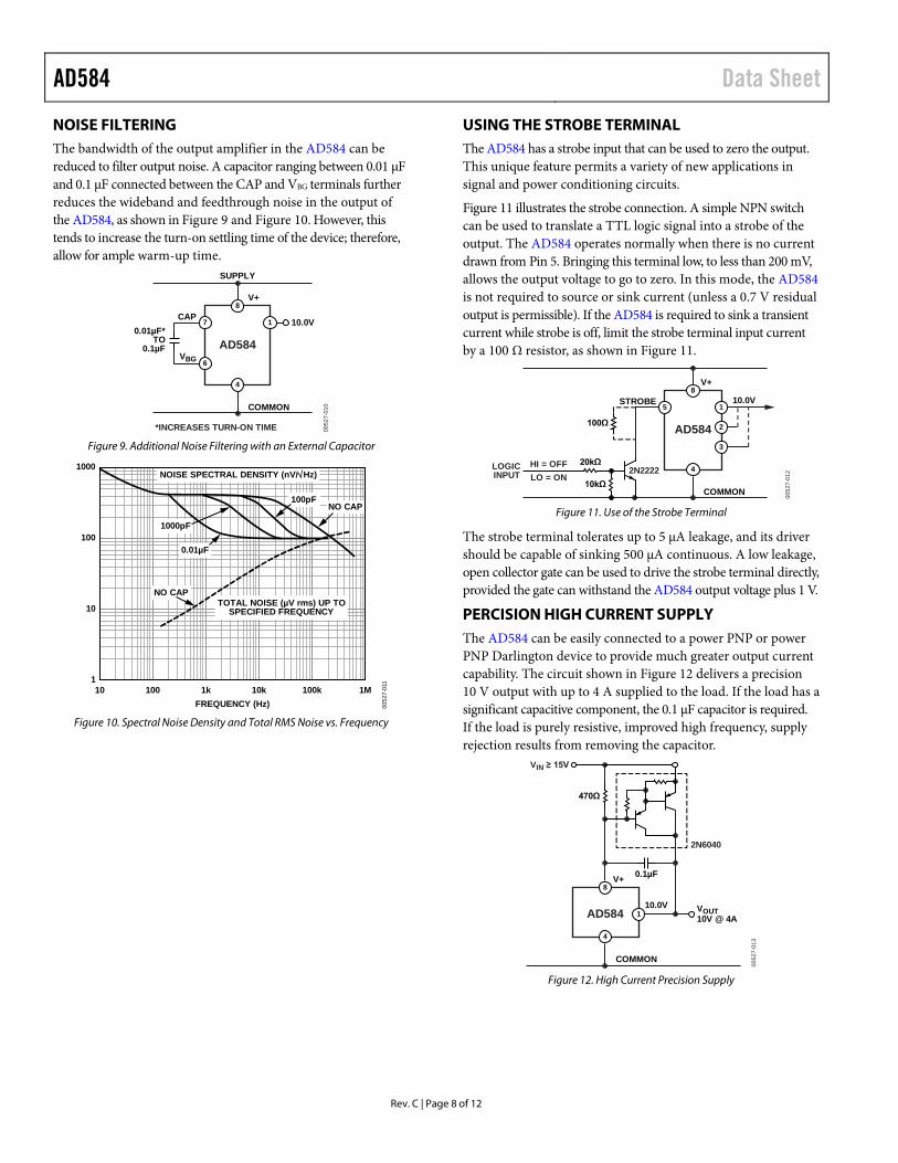
DYNAMIC PERFORMANCE Many low power instrument manufacturers are becoming increasingly concerned with the turn-on characteristics of the components being used in their systems. Fast turn-on components often enable the end user to keep power off when not needed and yet respond quickly when the power is turned on. Figure 8 displays the turn-on characteristic of the AD584. Figure 8 is generated from cold-start operation and represents the true turn-on waveform after an extended period with the supplies off. Figure 8 shows both the coarse and fine transient characteristics of the device; the total settling time to within ±10 mV is about 180 µs, and there is no long thermal tail appearing after the point.
Figure 8. Output Settling Characteristic
10.005
10.000
9.995–55 0 25 70 125
V OU
T (V
)
TEMPERATURE (°C) 0052
7-00
7
OUTPUT CURRENT (mA)
OU
TPU
T VO
LTA
GE
(V)
0 5 10 15 20–5–10–15SINKSOURCE
–20
14
12
10
8
6
4
2
0
+VS = 15VTA = 25°C
0052
7-00
8
SETTLING TIME (µs)100 150 200 250500
10.03V
10.02V
12V
11V
10V
20V
10V
0V
10.01V
10.00V
OUTPUT
OUTPUT
POWERSUPPLY
INPUT
0052
7-00
9
AD584 Data Sheet
Rev. C | Page 8 of 12
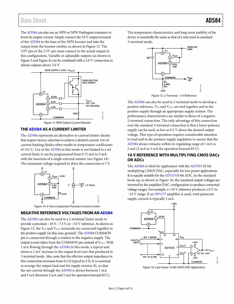
NOISE FILTERING The bandwidth of the output amplifier in the AD584 can be reduced to filter output noise. A capacitor ranging between 0.01 µF and 0.1 µF connected between the CAP and VBG terminals further reduces the wideband and feedthrough noise in the output of the AD584, as shown in Figure 9 and Figure 10. However, this tends to increase the turn-on settling time of the device; therefore, allow for ample warm-up time.
Figure 9. Additional Noise Filtering with an External Capacitor
Figure 10. Spectral Noise Density and Total RMS Noise vs. Frequency
USING THE STROBE TERMINAL The AD584 has a strobe input that can be used to zero the output. This unique feature permits a variety of new applications in signal and power conditioning circuits.
Figure 11 illustrates the strobe connection. A simple NPN switch can be used to translate a TTL logic signal into a strobe of the output. The AD584 operates normally when there is no current drawn from Pin 5. Bringing this terminal low, to less than 200 mV, allows the output voltage to go to zero. In this mode, the AD584 is not required to source or sink current (unless a 0.7 V residual output is permissible). If the AD584 is required to sink a transient current while strobe is off, limit the strobe terminal input current by a 100 Ω resistor, as shown in Figure 11.
Figure 11. Use of the Strobe Terminal
The strobe terminal tolerates up to 5 µA leakage, and its driver should be capable of sinking 500 µA continuous. A low leakage, open collector gate can be used to drive the strobe terminal directly, provided the gate can withstand the AD584 output voltage plus 1 V.
PERCISION HIGH CURRENT SUPPLY The AD584 can be easily connected to a power PNP or power PNP Darlington device to provide much greater output current capability. The circuit shown in Figure 12 delivers a precision 10 V output with up to 4 A supplied to the load. If the load has a significant capacitive component, the 0.1 µF capacitor is required. If the load is purely resistive, improved high frequency, supply rejection results from removing the capacitor.
Figure 12. High Current Precision Supply
AD584
1 10.0V
8
SUPPLY
V+
4
COMMON
7CAP
6VBG
0.01µF*TO
0.1µF
*INCREASES TURN-ON TIME 0052
7-01
0
1000
100
1
10
10 100 1k 10k 100k 1MFREQUENCY (Hz)
NOISE SPECTRAL DENSITY (nV/ Hz)
TOTAL NOISE (µV rms) UP TOSPECIFIED FREQUENCY
NO CAP
NO CAP100pF
1000pF
0.01µF
0052
7-01
1
AD584
110.0V
2
3
8V+
4
COMMON
5STROBE
10kΩ
20kΩ2N2222
100Ω
LOGICINPUT
HI = OFFLO = ON
0052
7-01
2
AD584 110.0V VOUT
10V @ 4A
8V+
4
COMMON
470Ω
0.1µF
VIN ≥ 15V
2N6040
0052
7-01
3
Data Sheet AD584
Rev. C | Page 9 of 12
The AD584 can also use an NPN or NPN Darlington transistor to boost its output current. Simply connect the 10 V output terminal of the AD584 to the base of the NPN booster and take the output from the booster emitter, as shown in Figure 13. The 5.0V pin or the 2.5V pin must connect to the actual output in this configuration. Variable or adjustable outputs (as shown in Figure 3 and Figure 4) can be combined with a 5.0 V connection to obtain outputs above 5.0 V.
Figure 13. NPN Output Current Booster
THE AD584 AS A CURRENT LIMITER The AD584 represents an alternative to current limiter diodes that require factory selection to achieve a desired current. Use of current limiting diodes often results in temperature coefficients of 1%/°C. Use of the AD584 in this mode is not limited to a set current limit; it can be programmed from 0.75 mA to 5 mA with the insertion of a single external resistor (see Figure 14). The minimum voltage required to drive the connection is 5 V.
Figure 14. A Two-Component Precision Current Limiter
NEGATIVE REFERENCE VOLTAGES FROM AN AD584 The AD584 can also be used in a 2-terminal Zener mode to provide a precision −10 V, −7.5 V, or −5.0 V reference. As shown in Figure 15, the VIN and VOUT terminals are connected together to the positive supply (in this case, ground). The AD584 COMMON pin is connected through a resistor to the negative supply. The output is now taken from the COMMON pin instead of VOUT. With 1 mA flowing through the AD584 in this mode, a typical unit shows a 2 mV increase in the output level over that produced in 3-terminal mode. Also, note that the effective output impedance in this connection increases from 0.2 Ω typical to 2 Ω. It is essential to arrange the output load and the supply resistor, RS, so that the net current through the AD584 is always between 1 mA and 5 mA (between 2 mA and 5 mA for operation beyond 85°C).
The temperature characteristics and long-term stability of the device is essentially the same as that of a unit used in standard 3-terminal mode.
Figure 15. 2-Terminal, −5 V Reference
The AD584 can also be used in 2-terminal mode to develop a positive reference. VIN and VOUT are tied together and to the positive supply through an appropriate supply resistor. The performance characteristics are similar to those of a negative 2-terminal connection. The only advantage of this connection over the standard 3-terminal connection is that a lower primary supply can be used, as low as 0.5 V above the desired output voltage. This type of operation requires considerable attention to load and to the primary supply regulation to ensure that the AD584 always remains within its regulating range of 1 mA to 5 mA (2 mA to 5 mA for operation beyond 85°C).
10 V REFERENCE WITH MULTIPLYING CMOS DACs OR ADCs The AD584 is ideal for application with the AD7533 10-bit multiplying CMOS DAC, especially for low power applications. It is equally suitable for the AD7574 8-bit ADC. In the standard hook-up, as shown in Figure 16, the standard output voltages are inverted by the amplifier/DAC configuration to produce converted voltage ranges. For example, a +10 V reference produces a 0 V to −10 V range. If an OP1177 amplifier is used, total quiescent supply current is typically 2 mA.
Figure 16. Low Power 10-Bit CMOS DAC Application
AD584
110.0V
5.0V
2.5V2
3
8V+
4COMMON
DARLINGTONNPN 2N6057
VOUT(5V, 12AAS SHOWN)
1kΩ
RAW SUPPLY (≈5V > VOUT)
0052
7-01
4
AD584
1VOUT = 2.5V
2.5VTAP
3
8V+
4COMMON
= i + 0.75mA2.5VR
RLOAD
0052
7-01
5
AD584
1VOUT
VREF–5V
5.0VTAP
2
8V+
4
COMMON
–15V
RS2.4kΩ5%
ANALOGGND
1µF
0052
7-01
6
AD58410.0V
V+
1
8
4
COMMON
+15V
AD7533
4BIT 1 (MSB)
5DIGITAL
INPUT
13
16
1
2BIT 10 (LSB)
15
3
14VREF
+15V
–15V
VOUT0V TO –10V
RFB
IOUT1
IOUT2
COMMON
0052
7-01
7
AD584 Data Sheet
Rev. C | Page 10 of 12
The AD584 is normally used in the −10 V mode with the AD7574 to give a 0 V to +10 V ADC range. This is shown in Figure 17. Bipolar output applications and other operating details can be found in the data sheets for the CMOS products.
Figure 17. AD584 as −10 V Reference for CMOS ADC
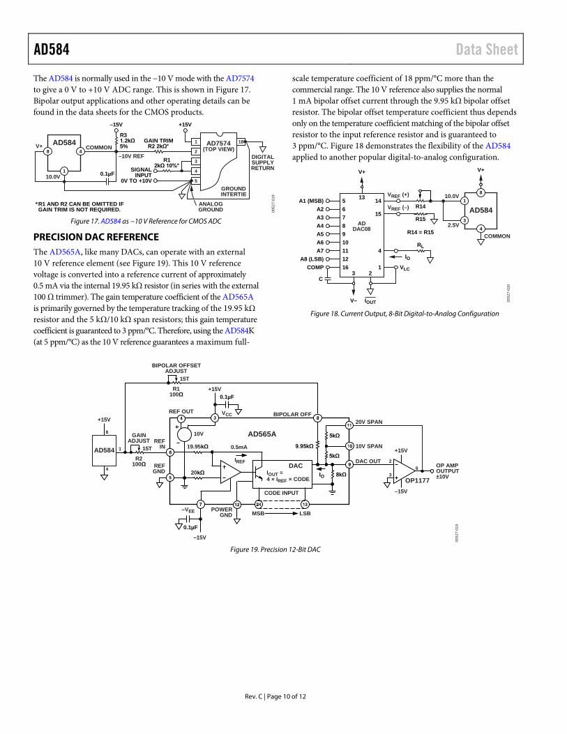
PRECISION DAC REFERENCE The AD565A, like many DACs, can operate with an external 10 V reference element (see Figure 19). This 10 V reference voltage is converted into a reference current of approximately 0.5 mA via the internal 19.95 kΩ resistor (in series with the external 100 Ω trimmer). The gain temperature coefficient of the AD565A is primarily governed by the temperature tracking of the 19.95 kΩ resistor and the 5 kΩ/10 kΩ span resistors; this gain temperature coefficient is guaranteed to 3 ppm/°C. Therefore, using the AD584K (at 5 ppm/°C) as the 10 V reference guarantees a maximum full-
scale temperature coefficient of 18 ppm/°C more than the commercial range. The 10 V reference also supplies the normal 1 mA bipolar offset current through the 9.95 kΩ bipolar offset resistor. The bipolar offset temperature coefficient thus depends only on the temperature coefficient matching of the bipolar offset resistor to the input reference resistor and is guaranteed to 3 ppm/°C. Figure 18 demonstrates the flexibility of the AD584 applied to another popular digital-to-analog configuration.
Figure 18. Current Output, 8-Bit Digital-to-Analog Configuration
Figure 19. Precision 12-Bit DAC
–10V REF
AD5844
1
8
–15V
V+
10.0V
COMMON
R31.2kΩ5%
0.1µF
+15V
1 18
2
3
4
5
AD7574(TOP VIEW)
SIGNALINPUT
0V TO +10V
ANALOGGROUND
GROUNDINTERTIE
DIGITALSUPPLYRETURN
R12kΩ 10%*
*R1 AND R2 CAN BE OMITTED IFGAIN TRIM IS NOT REQUIRED.
GAIN TRIMR2 2kΩ*
0052
7-01
9
C
A1 (MSB) 5 14A2 6
15A3 7A4 8A5 9A6 10A7 11 4
IOA8 (LSB) 12COMP 16 1 VLC
RL
R15
R14 = R15
V+
13
V–
3 2
ADDAC08
VREF (+)
VREF (–) AD584
4
8
1
3
COMMON
V+
2.5V
10.0V
R14
0052
7-02
0
IOUT
0052
7-01
8
0.5mA
IREFDAC
AD565A 5kΩ
20V SPAN
10V SPAN
DAC OUT
–VEE
REFGND
BIPOLAR OFF
5kΩ
8kΩIO
CODE INPUT
LSBMSB
10V
VCCREF OUT
REFIN
POWERGND
19.95kΩ
20kΩ
9.95kΩ
IOUT =4 × IREF × CODE
0.1µF
0.1µF
OP1177
+15V
–15V
2
36 OP AMP
OUTPUT±10V
+15V
+15V
1
4
8
AD584R2
100Ω
15T
GAINADJUST
R1100Ω
15T
BIPOLAR OFFSETADJUST
–15V
Data Sheet AD584
Rev. C | Page 11 of 12
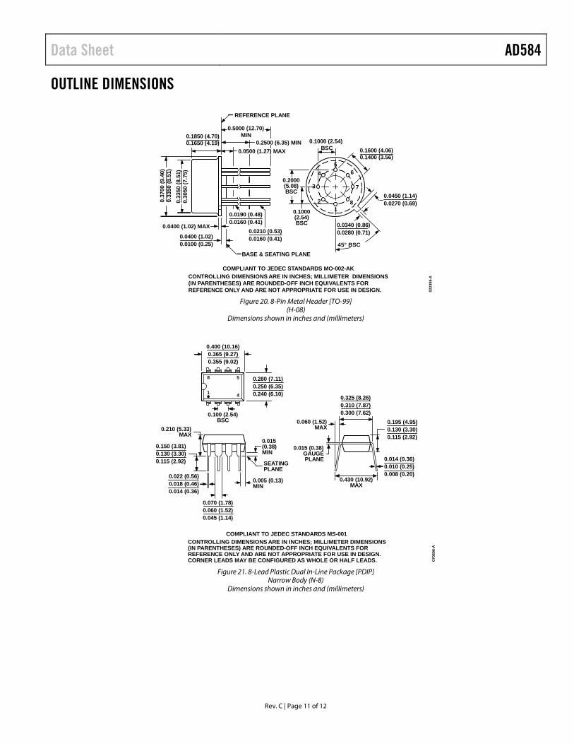
OUTLINE DIMENSIONS
Figure 20. 8-Pin Metal Header [TO-99]
(H-08) Dimensions shown in inches and (millimeters)
Figure 21. 8-Lead Plastic Dual In-Line Package [PDIP]
Narrow Body (N-8) Dimensions shown in inches and (millimeters)
CONTROLLING DIMENSIONS ARE IN INCHES; MILLIMETER DIMENSIONS(IN PARENTHESES) ARE ROUNDED-OFF INCH EQUIVALENTS FORREFERENCE ONLY AND ARE NOT APPROPRIATE FOR USE IN DESIGN.
COMPLIANT TO JEDEC STANDARDS MO-002-AK
0.2500 (6.35) MIN
0.5000 (12.70)MIN0.1850 (4.70)
0.1650 (4.19)
REFERENCE PLANE
0.0500 (1.27) MAX
0.0190 (0.48)0.0160 (0.41)
0.0210 (0.53)0.0160 (0.41)0.0400 (1.02)
0.0100 (0.25)
0.0400 (1.02) MAX 0.0340 (0.86)0.0280 (0.71)
0.0450 (1.14)0.0270 (0.69)
0.1600 (4.06)0.1400 (3.56)
0.1000 (2.54)BSC
6
2 8
7
54
3
1
0.2000(5.08)BSC
0.1000(2.54)BSC
0.37
00 (9
.40)
0.33
50 (8
.51)
0.33
50 (8
.51)
0.30
50 (7
.75)
45° BSCBASE & SEATING PLANE
0223
06-A
COMPLIANT TO JEDEC STANDARDS MS-001CONTROLLING DIMENSIONS ARE IN INCHES; MILLIMETER DIMENSIONS(IN PARENTHESES) ARE ROUNDED-OFF INCH EQUIVALENTS FORREFERENCE ONLY AND ARE NOT APPROPRIATE FOR USE IN DESIGN.CORNER LEADS MAY BE CONFIGURED AS WHOLE OR HALF LEADS. 07
0606
-A
0.022 (0.56)0.018 (0.46)0.014 (0.36)
SEATINGPLANE
0.015(0.38)MIN
0.210 (5.33)MAX
0.150 (3.81)0.130 (3.30)0.115 (2.92)
0.070 (1.78)0.060 (1.52)0.045 (1.14)
8
1 4
5 0.280 (7.11)0.250 (6.35)0.240 (6.10)
0.100 (2.54)BSC
0.400 (10.16)0.365 (9.27)0.355 (9.02)
0.060 (1.52)MAX
0.430 (10.92)MAX
0.014 (0.36)0.010 (0.25)0.008 (0.20)
0.325 (8.26)0.310 (7.87)0.300 (7.62)
0.195 (4.95)0.130 (3.30)0.115 (2.92)
0.015 (0.38)GAUGEPLANE
0.005 (0.13)MIN
AD584 Data Sheet
Rev. C | Page 12 of 12
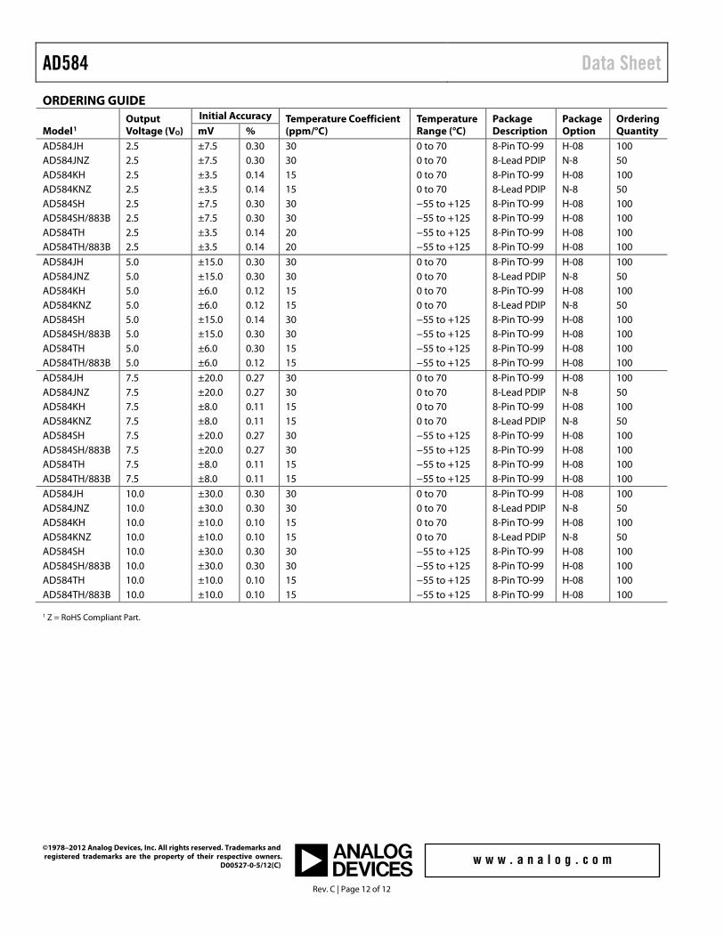
ORDERING GUIDE
Model1 Output Voltage (VO)
Initial Accuracy Temperature Coefficient (ppm/°C)
Temperature Range (°C)
Package Description
Package Option
Ordering Quantity mV %
AD584JH 2.5 ±7.5 0.30 30 0 to 70 8-Pin TO-99 H-08 100 AD584JNZ 2.5 ±7.5 0.30 30 0 to 70 8-Lead PDIP N-8 50 AD584KH 2.5 ±3.5 0.14 15 0 to 70 8-Pin TO-99 H-08 100 AD584KNZ 2.5 ±3.5 0.14 15 0 to 70 8-Lead PDIP N-8 50 AD584SH 2.5 ±7.5 0.30 30 −55 to +125 8-Pin TO-99 H-08 100 AD584SH/883B 2.5 ±7.5 0.30 30 −55 to +125 8-Pin TO-99 H-08 100 AD584TH 2.5 ±3.5 0.14 20 −55 to +125 8-Pin TO-99 H-08 100 AD584TH/883B 2.5 ±3.5 0.14 20 −55 to +125 8-Pin TO-99 H-08 100 AD584JH 5.0 ±15.0 0.30 30 0 to 70 8-Pin TO-99 H-08 100 AD584JNZ 5.0 ±15.0 0.30 30 0 to 70 8-Lead PDIP N-8 50 AD584KH 5.0 ±6.0 0.12 15 0 to 70 8-Pin TO-99 H-08 100 AD584KNZ 5.0 ±6.0 0.12 15 0 to 70 8-Lead PDIP N-8 50 AD584SH 5.0 ±15.0 0.14 30 −55 to +125 8-Pin TO-99 H-08 100 AD584SH/883B 5.0 ±15.0 0.30 30 −55 to +125 8-Pin TO-99 H-08 100 AD584TH 5.0 ±6.0 0.30 15 −55 to +125 8-Pin TO-99 H-08 100 AD584TH/883B 5.0 ±6.0 0.12 15 −55 to +125 8-Pin TO-99 H-08 100 AD584JH 7.5 ±20.0 0.27 30 0 to 70 8-Pin TO-99 H-08 100 AD584JNZ 7.5 ±20.0 0.27 30 0 to 70 8-Lead PDIP N-8 50 AD584KH 7.5 ±8.0 0.11 15 0 to 70 8-Pin TO-99 H-08 100 AD584KNZ 7.5 ±8.0 0.11 15 0 to 70 8-Lead PDIP N-8 50 AD584SH 7.5 ±20.0 0.27 30 −55 to +125 8-Pin TO-99 H-08 100 AD584SH/883B 7.5 ±20.0 0.27 30 −55 to +125 8-Pin TO-99 H-08 100 AD584TH 7.5 ±8.0 0.11 15 −55 to +125 8-Pin TO-99 H-08 100 AD584TH/883B 7.5 ±8.0 0.11 15 −55 to +125 8-Pin TO-99 H-08 100 AD584JH 10.0 ±30.0 0.30 30 0 to 70 8-Pin TO-99 H-08 100 AD584JNZ 10.0 ±30.0 0.30 30 0 to 70 8-Lead PDIP N-8 50 AD584KH 10.0 ±10.0 0.10 15 0 to 70 8-Pin TO-99 H-08 100 AD584KNZ 10.0 ±10.0 0.10 15 0 to 70 8-Lead PDIP N-8 50 AD584SH 10.0 ±30.0 0.30 30 −55 to +125 8-Pin TO-99 H-08 100 AD584SH/883B 10.0 ±30.0 0.30 30 −55 to +125 8-Pin TO-99 H-08 100 AD584TH 10.0 ±10.0 0.10 15 −55 to +125 8-Pin TO-99 H-08 100 AD584TH/883B 10.0 ±10.0 0.10 15 −55 to +125 8-Pin TO-99 H-08 100 1 Z = RoHS Compliant Part.
©1978–2012 Analog Devices, Inc. All rights reserved. Trademarks and registered trademarks are the property of their respective owners. D00527-0-5/12(C)