Embed Size (px)
Citation preview
VR4181™64-/32-bit Microprocessor
NEC Corporation 2000 MIPS Technologies, Inc. 1998Printed in Japan
Document No. U14272EJ1V0UMJ1 (1st edition)Date Published September 2000 NS CP(K)
User’s Manual
µµµµPD30181

User’s Manual U14272EJ1V0UM002
[MEMO]
User’s Manual U14272EJ1V0UM00 3
NOTES FOR CMOS DEVICES
1 PRECAUTION AGAINST ESD FOR SEMICONDUCTORS
Note:
Strong electric field, when exposed to a MOS device, can cause destruction of the gate oxide and
ultimately degrade the device operation. Steps must be taken to stop generation of static electricity
as much as possible, and quickly dissipate it once, when it has occurred. Environmental control
must be adequate. When it is dry, humidifier should be used. It is recommended to avoid using
insulators that easily build static electricity. Semiconductor devices must be stored and transported
in an anti-static container, static shielding bag or conductive material. All test and measurement
tools including work bench and floor should be grounded. The operator should be grounded using
wrist strap. Semiconductor devices must not be touched with bare hands. Similar precautions need
to be taken for PW boards with semiconductor devices on it.
2 HANDLING OF UNUSED INPUT PINS FOR CMOS
Note:
No connection for CMOS device inputs can be cause of malfunction. If no connection is provided
to the input pins, it is possible that an internal input level may be generated due to noise, etc., hence
causing malfunction. CMOS devices behave differently than Bipolar or NMOS devices. Input levels
of CMOS devices must be fixed high or low by using a pull-up or pull-down circuitry. Each unused
pin should be connected to VDD or GND with a resistor, if it is considered to have a possibility of
being an output pin. All handling related to the unused pins must be judged device by device and
related specifications governing the devices.
3 STATUS BEFORE INITIALIZATION OF MOS DEVICES
Note:
Power-on does not necessarily define initial status of MOS device. Production process of MOS
does not define the initial operation status of the device. Immediately after the power source is
turned ON, the devices with reset function have not yet been initialized. Hence, power-on does
not guarantee out-pin levels, I/O settings or contents of registers. Device is not initialized until the
reset signal is received. Reset operation must be executed immediately after power-on for devices
having reset function.
VR4000, VR4000 Series, V R4100, VR4100 Series, V R4102, VR4110, VR4111, VR4181, VR4300, VR4305,VR4310, VR4400, and VR Series are trademarks of NEC Corporation.MIPS is a registered trademark of MIPS Technologies, Inc. in the United States.UNIX is a registered trademark in the United States and other countries, licensed exclusively throughX/Open Company, Ltd.StrataFlash is a trademark of Intel Corp.
User’s Manual U14272EJ1V0UM004
Exporting this product or equipment that includes this product may require a governmental license from the U.S.A. for somecountries because this product utilizes technologies limited by the export control regulations of the U.S.A.
M8E 00. 4
The information in this document is current as of June, 2000. The information is subject to change without notice. For actual design-in, refer to the latest publications of NEC's data sheets or data books, etc., for the most up-to-date specifications of NEC semiconductor products. Not all products and/or types are available in every country. Please check with an NEC sales representative for availability and additional information.No part of this document may be copied or reproduced in any form or by any means without prior written consent of NEC. NEC assumes no responsibility for any errors that may appear in this document.NEC does not assume any liability for infringement of patents, copyrights or other intellectual property rights of third parties by or arising from the use of NEC semiconductor products listed in this document or any other liability arising from the use of such products. No license, express, implied or otherwise, is granted under any patents, copyrights or other intellectual property rights of NEC or others.Descriptions of circuits, software and other related information in this document are provided for illustrative purposes in semiconductor product operation and application examples. The incorporation of these circuits, software and information in the design of customer's equipment shall be done under the full responsibility of customer. NEC assumes no responsibility for any losses incurred by customers or third parties arising from the use of these circuits, software and information.While NEC endeavours to enhance the quality, reliability and safety of NEC semiconductor products, customers agree and acknowledge that the possibility of defects thereof cannot be eliminated entirely. To minimize risks of damage to property or injury (including death) to persons arising from defects in NEC semiconductor products, customers must incorporate sufficient safety measures in their design, such as redundancy, fire-containment, and anti-failure features.NEC semiconductor products are classified into the following three quality grades:"Standard", "Special" and "Specific". The "Specific" quality grade applies only to semiconductor products developed based on a customer-designated "quality assurance program" for a specific application. The recommended applications of a semiconductor product depend on its quality grade, as indicated below. Customers must check the quality grade of each semiconductor product before using it in a particular application. "Standard": Computers, office equipment, communications equipment, test and measurement equipment, audio
and visual equipment, home electronic appliances, machine tools, personal electronic equipmentand industrial robots
"Special": Transportation equipment (automobiles, trains, ships, etc.), traffic control systems, anti-disastersystems, anti-crime systems, safety equipment and medical equipment (not specifically designedfor life support)
"Specific": Aircraft, aerospace equipment, submersible repeaters, nuclear reactor control systems, lifesupport systems and medical equipment for life support, etc.
The quality grade of NEC semiconductor products is "Standard" unless otherwise expressly specified in NEC's data sheets or data books, etc. If customers wish to use NEC semiconductor products in applications not intended by NEC, they must contact an NEC sales representative in advance to determine NEC's willingness to support a given application.(Note)(1) "NEC" as used in this statement means NEC Corporation and also includes its majority-owned subsidiaries.(2) "NEC semiconductor products" means any semiconductor product developed or manufactured by or for
NEC (as defined above).
•
•
•
•
•
•
User’s Manual U14272EJ1V0UM00 5
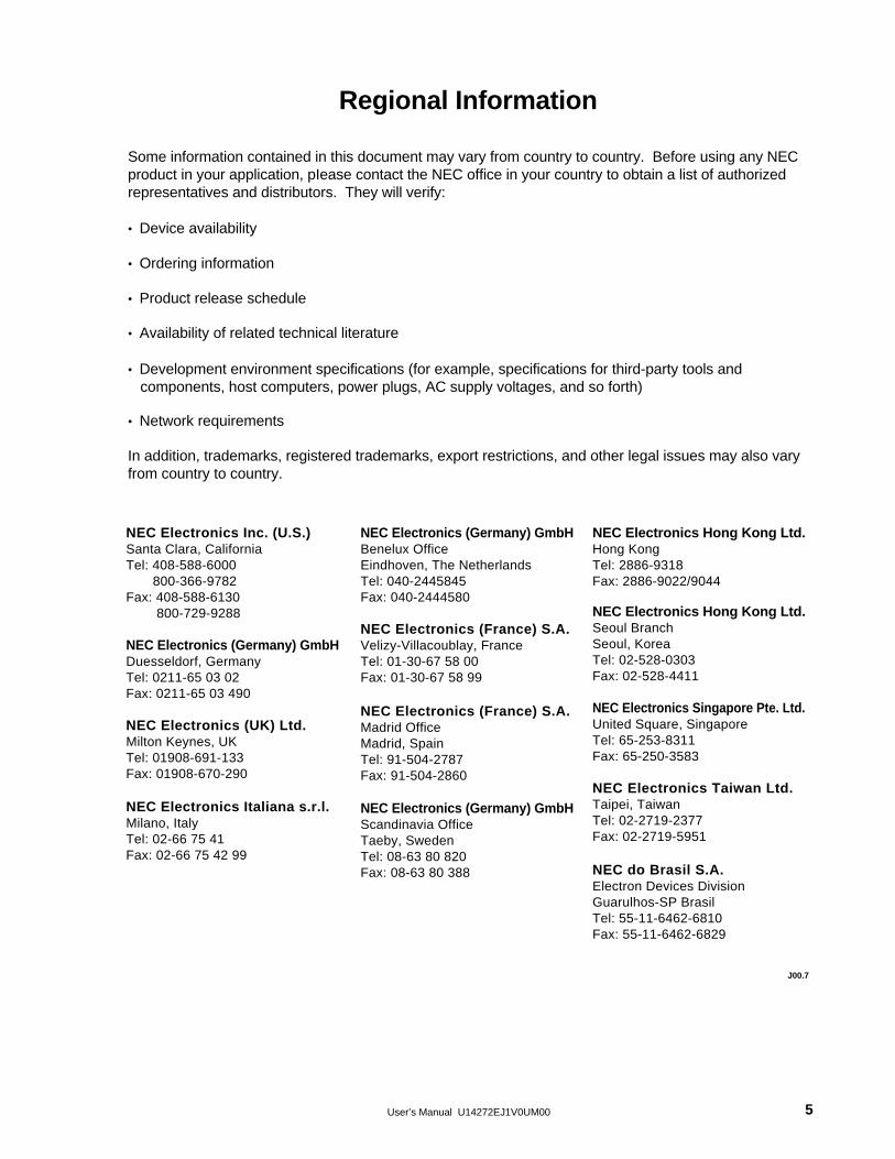
Regional Information
Some information contained in this document may vary from country to country. Before using any NECproduct in your application, pIease contact the NEC office in your country to obtain a list of authorizedrepresentatives and distributors. They will verify:
• Device availability
• Ordering information
• Product release schedule
• Availability of related technical literature
• Development environment specifications (for example, specifications for third-party tools and components, host computers, power plugs, AC supply voltages, and so forth)
• Network requirements
In addition, trademarks, registered trademarks, export restrictions, and other legal issues may also varyfrom country to country.
NEC Electronics Inc. (U.S.)Santa Clara, CaliforniaTel: 408-588-6000 800-366-9782Fax: 408-588-6130 800-729-9288
NEC Electronics (Germany) GmbHDuesseldorf, GermanyTel: 0211-65 03 02Fax: 0211-65 03 490
NEC Electronics (UK) Ltd.Milton Keynes, UKTel: 01908-691-133Fax: 01908-670-290
NEC Electronics Italiana s.r.l.Milano, ItalyTel: 02-66 75 41Fax: 02-66 75 42 99
NEC Electronics (Germany) GmbHBenelux OfficeEindhoven, The NetherlandsTel: 040-2445845Fax: 040-2444580
NEC Electronics (France) S.A.Velizy-Villacoublay, FranceTel: 01-30-67 58 00Fax: 01-30-67 58 99
NEC Electronics (France) S.A.Madrid OfficeMadrid, SpainTel: 91-504-2787Fax: 91-504-2860
NEC Electronics (Germany) GmbHScandinavia OfficeTaeby, SwedenTel: 08-63 80 820Fax: 08-63 80 388
NEC Electronics Hong Kong Ltd.Hong KongTel: 2886-9318Fax: 2886-9022/9044
NEC Electronics Hong Kong Ltd. Seoul BranchSeoul, KoreaTel: 02-528-0303Fax: 02-528-4411
NEC Electronics Singapore Pte. Ltd.United Square, SingaporeTel: 65-253-8311Fax: 65-250-3583
NEC Electronics Taiwan Ltd.Taipei, TaiwanTel: 02-2719-2377Fax: 02-2719-5951
NEC do Brasil S.A.Electron Devices DivisionGuarulhos-SP BrasilTel: 55-11-6462-6810Fax: 55-11-6462-6829
J00.7

User’s Manual U14272EJ1V0UM006
[MEMO]
User’s Manual U14272EJ1V0UM00 7
PREFACE
Readers This manual targets users who intend to understand the functions of the VR4181 andto design application systems using this microprocessor.
Purpose This manual introduces the architecture and hardware functions of the VR4181 tousers, following the organization described below.
Organization This manual consists of the following contents:
• Introduction• Pipeline operation• Cache organization and memory management system• Exception processing• Initialization interface• Interrupts• Peripheral units• Instruction set details
How to read this manual It is assumed that the reader of this manual has general knowledge in the fields ofelectric engineering, logic circuits, and microcomputers.
The VR4000TM in this manual includes the VR4400TM.
To learn in detail about the function of a specific instruction,→ Read CHAPTER 3 MIPSTM III INSTRUCTION SET SUMMARY, CHAPTER 4
MIPS16 INSTRUCTION SET, CHAPTER 27 MIPS III INSTRUCTION SETDETAILS , and CHAPTER 28 MIPS16 INSTRUCTION SET FORMAT .
To learn about the overall functions of the VR4181,→ Read this manual in sequential order.
To learn about electrical specifications,→ Refer to Data Sheet which is separately available.
Conventions Data significance: Higher on left and lower on rightActive low: XXX# (trailing # after pin and signal names)Note : Description of item marked with Note in the textCaution : Information requiring particular attentionRemark : Supplementary informationNumeric representation: binary/decimal ... XXXX
hexadecimal ... 0xXXXXPrefixes representing an exponent of 2 (for address space or memory capacity):
K (kilo) 210 = 1024M (mega) 220 = 10242
G (giga) 230 = 10243
T (tera) 240 = 10244
P (peta) 250 = 10245
E (exa) 260 = 10246
User’s Manual U14272EJ1V0UM008
Related Documents The related documents indicated here may include preliminary version. However,preliminary versions are not marked as such.
• User’s manualVR4181 User’s Manual This manual
• Data sheetµPD30181 (VR4181) Data Sheet U14273E
User’s Manual U14272EJ1V0UM00 9
CONTENTS
CHAPTER 1 INTRODUCTION ..................................................................................................... ........ 31
1.1 Features ................................................................................................................. .................. 311.2 Ordering Information ..................................................................................................... ......... 321.3 VR4181 Key Features ............................................................................................................. .. 32
1.3.1 CPU core ..................................................................................................................................... 33
1.3.2 Bus interface ............................................................................................................................... 33
1.3.3 Memory interface ........................................................................................................................ 34
1.3.4 DMA controller (DCU) ................................................................................................................. 34
1.3.5 Interrupt controller (ICU) ............................................................................................................. 34
1.3.6 Real-time clock ............................................................................................................................ 34
1.3.7 Audio output (D/A converter) ....................................................................................................... 34
1.3.8 Touch panel interface and audio input (A/D converter) ............................................................... 34
1.3.9 CompactFlash interface (ECU) ................................................................................................... 34
1.3.10 Primary serial interface (SIU1) .................................................................................................. 34
1.3.11 Secondary serial interface (SIU2) ............................................................................................. 34
1.3.12 Clocked serial interface (CSI) ................................................................................................... 35
1.3.13 Keyboard interface (KIU) ........................................................................................................... 35
1.3.14 General-purpose I/O ................................................................................................................. 35
1.3.15 Programmable chip selects ....................................................................................................... 36
1.3.16 LCD interface ............................................................................................................................ 36
1.3.17 Wake-up events ........................................................................................................................ 37
1.4 VR4110 CPU Core ................................................................................................................. ... 371.4.1 CPU registers .............................................................................................................................. 39
1.4.2 Coprocessors .............................................................................................................................. 40
1.4.3 Floating-point unit (FPU) ............................................................................................................. 42
1.4.4 CPU core memory management unit .......................................................................................... 42
1.4.5 Translation lookaside buffer (TLB) .............................................................................................. 42
1.4.6 Operating mode .......................................................................................................................... 42
1.4.7 Cache .......................................................................................................................................... 43
1.5 Instruction Pipeline ..................................................................................................... ............ 431.6 Clock Interface .......................................................................................................... ............... 43
CHAPTER 2 PIN FUNCTIONS ................................................................................................... ......... 45
2.1 Pin Configuration ........................................................................................................ ............ 452.2 Pin Function Description ................................................................................................. ....... 47
2.2.1 System bus interface signals ...................................................................................................... 47
2.2.2 LCD interface signals .................................................................................................................. 49
2.2.3 Initialization interface signals ...................................................................................................... 50
2.2.4 Battery monitor interface signals ................................................................................................. 50
2.2.5 Clock interface signals ................................................................................................................ 50
2.2.6 Touch panel interface and audio interface signals ...................................................................... 51
2.2.7 LED interface signals .................................................................................................................. 51
2.2.8 CompactFlash interface and keyboard interface signals ............................................................ 51
User’s Manual U14272EJ1V0UM0010
2.2.9 Serial interface 1 signals ............................................................................................................. 52
2.2.10 IrDA interface signals ................................................................................................................ 52
2.2.11 General-purpose I/O signals ..................................................................................................... 53
2.2.12 Dedicated VDD/GND signals ...................................................................................................... 54
2.3 Pin Status in Specific Status ............................................................................................ ...... 55
CHAPTER 3 MIPS III INSTRUCTION SET SUMMARY .................................................................... 59
3.1 CPU Instruction Formats .................................................................................................. ...... 593.2 Instruction Classes ...................................................................................................... ........... 60
3.2.1 Load and store instructions ......................................................................................................... 60
3.2.2 Computational instructions .......................................................................................................... 64
3.2.3 Jump and branch instructions ..................................................................................................... 70
3.2.4 Special instructions ..................................................................................................................... 74
3.2.5 System control coprocessor (CP0) instructions .......................................................................... 75
CHAPTER 4 MIPS16 INSTRUCTION SET ........................................................................................ 77
4.1 Outline .................................................................................................................. .................... 774.2 Features ................................................................................................................. ................... 774.3 Register Set ............................................................................................................. ................. 784.4 ISA Mode ................................................................................................................. ................. 79
4.4.1 Changing ISA mode bit by software ............................................................................................ 79
4.4.2 Changing ISA mode bit by exception .......................................................................................... 79
4.4.3 Enabling change ISA mode bit .................................................................................................... 80
4.5 Types of Instructions .................................................................................................... .......... 804.6 Instruction Format ....................................................................................................... ............ 824.7 MIPS16 Operation Code Bit Encoding .................................................................................. 874.8 Outline of Instructions .................................................................................................. .......... 90
4.8.1 PC-relative instructions ............................................................................................................... 90
4.8.2 Extend instruction ........................................................................................................................ 91
4.8.3 Delay slots ................................................................................................................................... 93
4.8.4 Instruction details ........................................................................................................................ 94
CHAPTER 5 VR4181 PIPELINE .......................................................................................................... 107
5.1 Pipeline Stages .......................................................................................................... .............. 1075.1.1 Pipeline activities ......................................................................................................................... 108
5.2 Branch Delay ............................................................................................................. ............... 1105.3 Load Delay ............................................................................................................... ................ 1105.4 Pipeline Operation ....................................................................................................... ............ 1105.5 Interlock and Exception Handling ......................................................................................... 117
5.5.1 Exception conditions ................................................................................................................... 120
5.5.2 Stall conditions ............................................................................................................................ 121
5.5.3 Slip conditions ............................................................................................................................. 122
5.5.4 Bypassing .................................................................................................................................... 124
5.6 Code Compatibility ....................................................................................................... ........... 124
User’s Manual U14272EJ1V0UM00 11
CHAPTER 6 MEMORY MANAGEMENT SYSTEM ........................................................................... 125
6.1 Translation Lookaside Buffer (TLB) ...................................................................................... 1 256.2 Virtual Address Space .................................................................................................... ........ 125
6.2.1 Virtual-to-physical address translation ........................................................................................ 126
6.2.2 32-bit mode address translation .................................................................................................. 127
6.2.3 64-bit mode address translation .................................................................................................. 128
6.2.4 Operating modes ......................................................................................................................... 129
6.2.5 User mode virtual addressing ..................................................................................................... 129
6.2.6 Supervisor mode virtual addressing ............................................................................................ 131
6.2.7 Kernel mode virtual addressing ................................................................................................... 134
6.3 Physical Address Space .................................................................................................. ...... 1426.3.1 ROM space ................................................................................................................................. 143
6.3.2 External system bus space ......................................................................................................... 143
6.3.3 Internal I/O space ........................................................................................................................ 144
6.3.4 DRAM space ............................................................................................................................... 145
6.4 System Control Coprocessor ............................................................................................... . 1466.4.1 Format of a TLB entry ................................................................................................................. 147
6.5 CP0 Registers ............................................................................................................ .............. 1486.5.1 Index register (0) ......................................................................................................................... 148
6.5.2 Random register (1) .................................................................................................................... 148
6.5.3 EntryLo0 (2) and EntryLo1 (3) registers ...................................................................................... 149
6.5.4 PageMask register (5) ................................................................................................................. 150
6.5.5 Wired register (6) ........................................................................................................................ 151
6.5.6 EntryHi register (10) .................................................................................................................... 152
6.5.7 Processor revision identifier (PRId) register (15) ........................................................................ 153
6.5.8 Config register (16) ..................................................................................................................... 154
6.5.9 Load linked address (LLAddr) register (17) ................................................................................. 155
6.5.10 Cache tag registers (TagLo (28) and TagHi (29)) ..................................................................... 156
6.5.11 Virtual-to-physical address translation ...................................................................................... 157
6.5.12 TLB misses ............................................................................................................................... 159
6.5.13 TLB instructions ........................................................................................................................ 159
CHAPTER 7 EXCEPTION PROCESSING .......................................................................................... 161
7.1 Exception Processing Operation ........................................................................................... 1617.2 Precision of Exceptions .................................................................................................. ........ 1627.3 Exception Processing Registers ........................................................................................... 163
7.3.1 Context register (4) ..................................................................................................................... 164
7.3.2 BadVAddr register (8) ................................................................................................................. 165
7.3.3 Count register (9) ........................................................................................................................ 165
7.3.4 Compare register (11) ................................................................................................................. 166
7.3.5 Status register (12) ...................................................................................................................... 166
7.3.6 Cause register (13) ..................................................................................................................... 169
7.3.7 Exception program counter (EPC) register (14) .......................................................................... 171
7.3.8 WatchLo (18) and WatchHi (19) registers ................................................................................... 172
7.3.9 XContext register (20) ................................................................................................................. 173
7.3.10 Parity Error register (26) ............................................................................................................ 174
User’s Manual U14272EJ1V0UM0012
7.3.11 Cache Error register (27) ........................................................................................................... 174
7.3.12 ErrorEPC register (30) ............................................................................................................... 175
7.4 Details of Exceptions .................................................................................................... .......... 1777.4.1 Exception types ........................................................................................................................... 177
7.4.2 Exception vector locations ........................................................................................................... 177
7.4.3 Priority of exceptions ................................................................................................................... 179
7.4.4 Cold Reset exception .................................................................................................................. 180
7.4.5 Soft Reset exception ................................................................................................................... 181
7.4.6 NMI exception ............................................................................................................................. 182
7.4.7 Address Error exception .............................................................................................................. 183
7.4.8 TLB exceptions ............................................................................................................................ 184
7.4.9 Bus Error exception ..................................................................................................................... 187
7.4.10 System Call exception ............................................................................................................... 188
7.4.11 Breakpoint exception ................................................................................................................. 189
7.4.12 Coprocessor Unusable exception ............................................................................................. 190
7.4.13 Reserved Instruction exception ................................................................................................. 191
7.4.14 Trap exception ........................................................................................................................... 192
7.4.15 Integer Overflow exception ........................................................................................................ 192
7.4.16 Watch exception ........................................................................................................................ 193
7.4.17 Interrupt exception ..................................................................................................................... 194
7.5 Exception Processing and Servicing Flowcharts ................................................................ 195
CHAPTER 8 INITIALIZATION INTERFACE ....................................................................................... 2 03
8.1 Overview ................................................................................................................. .................. 2038.2 Reset Function ........................................................................................................... .............. 203
8.2.1 RTC reset .................................................................................................................................... 204
8.2.2 RSTSW ....................................................................................................................................... 205
8.2.3 Deadman’s Switch ....................................................................................................................... 206
8.2.4 Software shutdown ...................................................................................................................... 207
8.2.5 HALTimer shutdown .................................................................................................................... 208
8.3 Power On Sequence ........................................................................................................ ........ 2098.4 Reset of CPU Core ........................................................................................................ ........... 211
8.4.1 Cold Reset ................................................................................................................................... 211
8.4.2 Soft Reset .................................................................................................................................... 212
8.5 VR4181 Processor Modes ....................................................................................................... 2138.5.1 Power modes .............................................................................................................................. 213
8.5.2 Privilege mode ............................................................................................................................. 214
8.5.3 Reverse endian ........................................................................................................................... 214
8.5.4 Bootstrap exception vector (BEV) ............................................................................................... 214
8.5.5 Cache error check ....................................................................................................................... 215
8.5.6 Parity error prohibit ...................................................................................................................... 215
8.5.7 Interrupt enable (IE) .................................................................................................................... 215
User’s Manual U14272EJ1V0UM00 13
CHAPTER 9 CACHE MEMORY .................................................................................................... ...... 217
9.1 Memory Organization ...................................................................................................... ....... 2179.2 Cache Organization ....................................................................................................... ......... 218
9.2.1 Organization of the instruction cache (I-cache) ........................................................................... 218
9.2.2 Organization of the data cache (D-cache) .................................................................................. 219
9.2.3 Accessing the caches ................................................................................................................. 220
9.3 Cache Operations ......................................................................................................... ........... 2219.3.1 Cache write policy ....................................................................................................................... 221
9.4 Cache States ............................................................................................................. ............... 2229.5 Cache State Transition Diagrams .......................................................................................... 223
9.5.1 Data cache state transition .......................................................................................................... 223
9.5.2 Instruction cache state transition ..................................................................................... ........... 223
9.6 Cache Data Integrity ..................................................................................................... ........... 2249.7 Manipulation of the Caches by an External Agent ............................................................... 232
CHAPTER 10 CPU CORE INTERRUPTS .......................................................................................... 233
10.1 Non-maskable Interrupt (NMI) ............................................................................................ .. 23310.2 Ordinary Interrupts ..................................................................................................... ........... 23310.3 Software Interrupts Generated in CPU Core ...................................................................... 23410.4 Timer Interrupt ......................................................................................................... .............. 23410.5 Asserting Interrupts .................................................................................................... .......... 234
10.5.1 Detecting hardware interrupts ................................................................................................... 234
10.5.2 Masking interrupt signals .......................................................................................................... 236
CHAPTER 11 BUS CONTROL .................................................................................................... ....... 237
11.1 MBA Host Bridge ......................................................................................................... .......... 23711.1.1 MBA Host Bridge ROM and register address space ................................................................. 238
11.1.2 MBA modules address space ................................................................................................... 238
11.2 Bus Control Registers ................................................................................................... ....... 23911.2.1 BCUCNTREG 1 (0x0A00 0000) ................................................................................................ 240
11.2.2 CMUCLKMSK (0x0A00 0004) ................................................................................................... 241
11.2.3 BCUSPEEDREG (0x0A00 000C) .............................................................................................. 242
11.2.4 BCURFCNTREG (0x0A00 0010) .............................................................................................. 244
11.2.5 REVIDREG (0x0A00 0014) ....................................................................................................... 245
11.2.6 CLKSPEEDREG (0x0A00 0018) ............................................................................................... 246
11.3 ROM Interface ........................................................................................................... ............. 24711.3.1 External ROM devices memory mapping .................................................................................. 247
11.3.2 Connection to external ROM (x 16) devices ............................................................................. 248
11.3.3 Example of ROM connection .................................................................................................... 249
11.3.4 External ROM cycles ................................................................................................................. 254
11.4 DRAM Interface .......................................................................................................... ............ 25711.4.1 EDO DRAM configuration ......................................................................................................... 257
11.4.2 Mix memory mode (EDO DRAM only) ....................................................................................... 258
11.4.3 EDO DRAM timing parameters ................................................................................................. 258
11.4.4 SDRAM configuration ................................................................................................................ 259
User’s Manual U14272EJ1V0UM0014
11.5 Memory Controller Register Set .......................................................................................... . 26011.5.1 EDOMCYTREG (0x0A00 0300) ................................................................................................ 260
11.5.2 MEMCFG_REG (0x0A00 0304) ................................................................................................ 262
11.5.3 MODE_REG (0x0A00 0308) ..................................................................................................... 264
11.5.4 SDTIMINGREG (0x0A00 030C) ................................................................................................ 265
11.6 ISA Bridge .............................................................................................................. ................ 26611.7 ISA Bridge Register Set ................................................................................................. ....... 266
11.7.1 ISABRGCTL (0x0B00 02C0) ..................................................................................................... 266
11.7.2 ISABRGSTS (0x0B00 02C2) ..................................................................................................... 267
11.7.3 XISACTL (0x0B00 02C4) .......................................................................................................... 268
CHAPTER 12 DMA CONTROL UNIT (DCU) .................................................................................... 271
12.1 General ................................................................................................................. .................. 27112.2 DCU Registers .......................................................................................................... ............ 273
12.2.1 Microphone destination 1 address registers .............................................................................. 274
12.2.2 Microphone destination 2 address registers .............................................................................. 275
12.2.3 Speaker source 1 address registers .......................................................................................... 276
12.2.4 Speaker source 2 address registers .......................................................................................... 277
12.2.5 DMARSTREG (0x0A00 0040) ................................................................................................... 278
12.2.6 AIUDMAMSKREG (0x0A00 0046) ............................................................................................. 278
12.2.7 MICRCLENREG (0x0A00 0658) ............................................................................................... 279
12.2.8 SPKRCLENREG (0x0A00 065A) .............................................................................................. 279
12.2.9 MICDMACFGREG (0x0A00 065E) ............................................................................................ 280
12.2.10 SPKDMACFGREG (0x0A00 0660) .......................................................................................... 281
12.2.11 DMAITRQREG (0x0A00 0662) ................................................................................................ 282
12.2.12 DMACLTREG (0x0A00 0664) ................................................................................................. 283
12.2.13 DMAITMKREG (0x0A00 0666) ................................................................................................ 284
CHAPTER 13 CLOCKED SERIAL INTERFACE UNIT (CSI) .......................................................... 285
13.1 Overview ................................................................................................................ ................. 28513.2 Operation of CSI ........................................................................................................ ............ 285
13.2.1 Transmit / receive operations .................................................................................................... 285
13.2.2 SCK phase and CSI transfer timing ........................................................................................... 286
13.2.3 CSI Transfer Types ................................................................................................................... 287
13.2.4 Transmit and receive FIFOs ...................................................................................................... 288
13.3 CSI Registers ........................................................................................................... .............. 28813.3.1 CSIMODE (0x0B00 0900) ......................................................................................................... 289
13.3.2 CSIRXDATA (0x0B00 0902) ..................................................................................................... 291
13.3.3 CSITXDATA (0x0B00 0904) ...................................................................................................... 291
13.3.4 CSILSTAT (0x0B00 0906) ......................................................................................................... 292
13.3.5 CSIINTMSK (0x0B00 0908) ...................................................................................................... 294
13.3.6 CSIINTSTAT (0x0B00 090A) ..................................................................................................... 295
13.3.7 CSITXBLEN (0x0B00 090C) ..................................................................................................... 297
13.3.8 CSIRXBLEN (0x0B00 090E) ..................................................................................................... 298
User’s Manual U14272EJ1V0UM00 15
CHAPTER 14 INTERRUPT CONTROL UNIT (ICU) ......................................................................... 299
14.1 Overview ................................................................................................................ ................ 29914.2 Register Set ............................................................................................................ ............... 301
14.2.1 SYSINT1REG (0x0A00 0080) ................................................................................................... 302
14.2.2 MSYSINT1REG (0x0A00 008C) ............................................................................................... 304
14.2.3 NMIREG (0x0A00 0098) ........................................................................................................... 306
14.2.4 SOFTINTREG (0x0A00 009A) .................................................................................................. 307
14.2.5 SYSINT2REG (0x0A00 0200) ................................................................................................... 308
14.2.6 MSYSINTREG2 (0x0A00 0206) ................................................................................................ 309
14.2.7 PIUINTREG (0x0B00 0082) ...................................................................................................... 310
14.2.8 AIUINTREG (0x0B00 0084) ...................................................................................................... 311
14.2.9 MPIUINTREG (0x0B00 008E) ................................................................................................... 312
14.2.10 MAIUINTREG (0x0B00 0090) ................................................................................................. 313
14.2.11 MKIUINTREG (0x0B00 0092) ................................................................................................. 314
14.2.12 KIUINTREG (0x0B00 0198) .................................................................................................... 315
CHAPTER 15 POWER MANAGEMENT UNIT (PMU) ...................................................................... 317
15.1 General ................................................................................................................. .................. 31715.2 Reset Control ........................................................................................................... .............. 317
15.2.1 RTC reset .................................................................................................................................. 318
15.2.2 RSTSW reset ............................................................................................................................ 318
15.2.3 Preserving DRAM data on RSTSW reset .................................................................................. 318
15.3 Shutdown Control ........................................................................................................ ......... 31915.3.1 HALTimer shutdown .................................................................................................................. 319
15.3.2 Deadman’s SW shutdown ......................................................................................................... 319
15.3.3 Software shutdown .................................................................................................................... 319
15.3.4 BATTINH shutdown .................................................................................................................. 319
15.4 Power-on Control ........................................................................................................ .......... 32015.4.1 Activation via Power Switch interrupt request ........................................................................... 321
15.4.2 Activation via CompactFlash interrupt request ......................................................................... . 322
15.4.3 Activation via GPIO Activation interrupt request ....................................................................... 323
15.4.4 Activation via DCD Interrupt ...................................................................................................... 324
15.4.5 Activation via Elapsed Timer interrupt (alarm interrupt) ............................................................ 326
15.5 DRAM Interface Control .................................................................................................. ...... 32715.5.1 System request to enter Hibernate mode (EDO DRAM) ........................................................... 327
15.5.2 System request to enter Hibernate mode (SDRAM) ................................................................. 328
15.5.3 Wake-up from Hibernate mode (EDO DRAM) ........................................................................... 328
15.5.4 Wake-up from Hibernate mode (SDRAM) ................................................................................. 329
15.5.5 Suspend mode .......................................................................................................................... 329
15.6 Register Set ............................................................................................................ ............... 33015.6.1 PMUINTREG (0x0B00 00A0) .................................................................................................... 331
15.6.2 PMUCNTREG (0x0B00 00A2) .................................................................................................. 333
15.6.3 PMUWAITREG (0x0B00 00A8) ................................................................................................. 335
15.6.4 PMUDIVREG (0x0B00 00AC) ................................................................................................... 336
15.6.5 DRAMHIBCTL (0x0B00 00B2) .................................................................................................. 337
User’s Manual U14272EJ1V0UM0016
15.7 VR4181 Power Mode .............................................................................................................. 3 3815.7.1 Power mode and state transition ............................................................................................... 338
CHAPTER 16 REALTIME CLOCK UNIT (RTC) ............................................................................... 341
16.1 General ................................................................................................................. .................. 34116.2 Register Set ............................................................................................................ ................ 342
16.2.1 Elapsed Time registers .............................................................................................................. 343
16.2.2 Elapsed Time compare registers ............................................................................................... 345
16.2.3 RTC Long 1 registers ................................................................................................................ 347
16.2.4 RTC Long 1 Count registers ...................................................................................................... 349
16.2.5 RTC Long 2 registers ................................................................................................................ 351
16.2.6 RTC Long 2 Count registers ...................................................................................................... 353
16.2.7 RTC interrupt register ................................................................................................................ 355
CHAPTER 17 DEADMAN’S SWITCH UNIT (DSU) .......................................................................... 357
17.1 General ................................................................................................................. .................. 35717.2 Register Set ............................................................................................................ ................ 357
17.2.1 DSUCNTREG (0x0B00 00E0) ................................................................................................... 358
17.2.2 DSUSETREG (0x0B00 00E2) ................................................................................................... 359
17.2.3 DSUCLRREG (0x0B00 00E4) ................................................................................................... 360
17.2.4 DSUTIMREG (0x0B00 00E6) .................................................................................................... 361
17.3 Register Setting Flow ................................................................................................... ......... 362
CHAPTER 18 GENERAL PURPOSE I/O UNIT (GIU) ...................................................................... 363
18.1 Overview ................................................................................................................ ................. 36318.1.1 GPIO pins and alternate functions ............................................................................................ 363
18.1.2 Pin direction control ................................................................................................................... 365
18.1.3 Non-volatile registers ................................................................................................................. 365
18.2 Alternate Functions Overview ............................................................................................ .. 36618.2.1 Clocked serial interface (CSI) .................................................................................................... 366
18.2.2 Primary and secondary serial (RS-232-C) interface .................................................................. 366
18.2.3 LCD interface ............................................................................................................................ 368
18.2.4 Programmable chip selects ....................................................................................................... 369
18.2.5 16-bit cycle support ................................................................................................................... 369
18.2.6 General purpose input/output .................................................................................................... 370
18.2.7 Interrupt requests and wake-up events ..................................................................................... 370
18.3 Register Set ............................................................................................................ ................ 37118.3.1 GPMD0REG (0x0B00 0300) ..................................................................................................... 373
18.3.2 GPMD1REG (0x0B00 0302) ..................................................................................................... 375
18.3.3 GPMD2REG (0x0B00 0304) ..................................................................................................... 377
18.3.4 GPMD3REG (0x0B00 0306) ..................................................................................................... 379
18.3.5 GPDATHREG (0x0B00 0308) ................................................................................................... 381
18.3.6 GPDATLREG (0x0B00 030A) ................................................................................................... 382
User’s Manual U14272EJ1V0UM00 17
18.3.7 GPINTEN (0x0B00 030C) ......................................................................................................... 383
18.3.8 GPINTMSK (0x0B00 030E) ....................................................................................................... 384
18.3.9 GPINTTYPH (0x0B00 0310) ..................................................................................................... 385
18.3.10 GPINTTYPL (0x0B00 0312) .................................................................................................... 387
18.3.11 GPINTSTAT (0x0B00 0314) .................................................................................................... 389
18.3.12 GPHIBSTH (0x0B00 0316) ..................................................................................................... 390
18.3.13 GPHIBSTL (0x0B00 0318) ...................................................................................................... 391
18.3.14 GPSICTL (0x0B00 031A) ........................................................................................................ 392
18.3.15 KEYEN (0x0B00 031C) ........................................................................................................... 394
18.3.16 PCS0STRA (0x0B00 0320) ..................................................................................................... 395
18.3.17 PCS0STPA (0x0B00 0322) ..................................................................................................... 395
18.3.18 PCS0HIA (0x0B00 0324) ........................................................................................................ 396
18.3.19 PCS1STRA (0x0B00 0326) ..................................................................................................... 397
18.3.20 PCS1STPA (0x0B00 0328) ..................................................................................................... 397
18.3.21 PCS1HIA (0x0B00 032A) ........................................................................................................ 398
18.3.22 PCSMODE (0x0B00 032C) ..................................................................................................... 399
18.3.23 LCDGPMODE (0x0B00 032E) ................................................................................................ 400
18.3.24 MISCREGn (0x0B00 0330 to 0x0B00 034E) .......................................................................... 401
CHAPTER 19 TOUCH PANEL INTERFACE UNIT (PIU) ................................................................ 403
19.1 General ................................................................................................................. .................. 40319.1.1 Block diagrams .......................................................................................................................... 404
19.2 Scan Sequencer State Transition ........................................................................................ 4 0619.3 Register Set ............................................................................................................ ............... 408
19.3.1 PIUCNTREG (0x0B00 0122) ..................................................................................................... 409
19.3.2 PIUINTREG (0x0B00 0124) ...................................................................................................... 412
19.3.3 PIUSIVLREG (0x0B00 0126) .................................................................................................... 413
19.3.4 PIUSTBLREG (0x0B00 0128) ................................................................................................... 414
19.3.5 PIUCMDREG (0x0B00 012A) ................................................................................................... 415
19.3.6 PIUASCNREG (0x0B00 0130) .................................................................................................. 417
19.3.7 PIUAMSKREG (0x0B00 0132) .................................................................................................. 419
19.3.8 PIUCIVLREG (0x0B00 013E) .................................................................................................... 420
19.3.9 PIUPBnmREG (0x0B00 02A0 to 0x0B00 02AE, 0x0B00 02BC to 0x0B00 02BE) .................... 421
19.3.10 PIUABnREG (0x0B00 02B0 to 0x0B00 02B6) ........................................................................ 422
19.4 Register Setting Flow ................................................................................................... ........ 42319.5 Relationships among TPX, TPY, ADIN, and AUDIOIN Pins and States ........................... 42519.6 Timing .................................................................................................................. ................... 426
19.6.1 Touch/release detection timing ................................................................................................. 426
19.6.2 A/D port scan timing .................................................................................................................. 426
19.7 Data Loss Interrupt Conditions .......................................................................................... . 427
CHAPTER 20 AUDIO INTERFACE UNIT (AIU) ............................................................................... 429
20.1 General ................................................................................................................. .................. 42920.2 Register Set ............................................................................................................ ............... 429
20.2.1 MDMADATREG (0x0B00 0160) ................................................................................................ 430
20.2.2 SDMADATREG (0x0B00 0162) ................................................................................................ 431
User’s Manual U14272EJ1V0UM0018
20.2.3 DAVREF_SETUP (0x0B00 0164) ............................................................................................. 432
20.2.4 SODATREG (0x0B00 0166) ...................................................................................................... 433
20.2.5 SCNTREG (0x0B00 0168) ........................................................................................................ 434
20.2.6 SCNVC_END (0x0B00 016E) ................................................................................................... 435
20.2.7 MIDATREG (0x0B00 0170) ....................................................................................................... 436
20.2.8 MCNTREG (0x0B00 0172) ........................................................................................................ 437
20.2.9 DVALIDREG (0x0B00 0178) ..................................................................................................... 438
20.2.10 SEQREG (0x0B00 017A) ........................................................................................................ 439
20.2.11 INTREG (0x0B00 017C) .......................................................................................................... 440
20.2.12 MCNVC_END (0x0B00 017E) ................................................................................................. 441
20.3 Operation Sequence ..................................................................................................... ........ 44220.3.1 Output (speaker) ....................................................................................................................... 442
20.3.2 Input (microphone) ................................................................................................................... 443
CHAPTER 21 KEYBOARD INTERFACE UNIT (KIU) ....................................................................... 445
21.1 General ................................................................................................................. .................. 44521.2 Functional Description .................................................................................................. ........ 445
21.2.1 Automatic keyboard scan mode ................................................................................................ 445
21.2.2 Manual keyboard scan mode .................................................................................................... 446
21.2.3 Key press detection ................................................................................................................... 446
21.2.4 Scan operation .......................................................................................................................... 447
21.2.5 Reading return data ................................................................................................................... 447
21.2.6 Interrupts and status reporting .................................................................................................. 448
21.3 Register Set ............................................................................................................ ................ 44921.3.1 KIUDATn (0x0B00 0180 to 0x0B00 018E) ................................................................................ 450
21.3.2 KIUSCANREP (0x0B00 0190) ................................................................................................... 451
21.3.3 KIUSCANS (0x0B00 0192) ........................................................................................................ 452
21.3.4 KIUWKS (0x0B00 0194) ............................................................................................................ 453
21.3.5 KIUWKI (0x0B00 0196) ............................................................................................................. 454
21.3.6 KIUINT (0x0B00 0198) .............................................................................................................. 455
CHAPTER 22 COMPACTFLASH CONTROLLER (ECU) ................................................................. 457
22.1 General ................................................................................................................. .................. 45722.2 Register Set Summary .................................................................................................... ...... 45722.3 ECU Control Registers ................................................................................................... ....... 460
22.3.1 INTSTATREG (0x0B00 08F8) ................................................................................................... 460
22.3.2 INTMSKREG (0x0B00 08FA) .................................................................................................... 461
22.3.3 CFG_REG_1 (0x0B00 08FE) .................................................................................................... 462
22.4 ECU Registers ........................................................................................................... ............. 46322.4.1 ID_REV_REG (Index: 0x00) ...................................................................................................... 463
22.4.2 IF_STAT_REG (Index: 0x01) .................................................................................................... 464
22.4.3 PWRRSETDRV (Index: 0x02) ................................................................................................... 465
22.4.4 ITGENCTREG (Index: 0x03) ..................................................................................................... 466
22.4.5 CDSTCHGREG (Index: 0x04) ................................................................................................... 467
22.4.6 CRDSTATREG (Index: 0x05) .................................................................................................... 468
22.4.7 ADWINENREG (Index: 0x06) .................................................................................................... 469
User’s Manual U14272EJ1V0UM00 19
22.4.8 IOCTRL_REG (Index: 0x07) ..................................................................................................... 470
22.4.9 IOADSLBnREG (Index: 0x08, 0x0C) ......................................................................................... 471
22.4.10 IOADSHBnREG (Index: 0x09, 0x0D) ...................................................................................... 471
22.4.11 IOSLBnREG (Index: 0x0A, 0x0E) ........................................................................................... 472
22.4.12 IOSHBnREG (Index: 0x0B, 0x0F) ........................................................................................... 472
22.4.13 SYSMEMSLnREG (Index: 0x10, 0x18, 0x20, 0x28, 0x30) ..................................................... 473
22.4.14 MEMWIDn_REG (Index: 0x11, 0x19, 0x21, 0x29, 0x31) ........................................................ 473
22.4.15 SYSMEMELnREG (Index: 0x12, 0x1A, 0x22, 0x2A, 0x32) ..................................................... 474
22.4.16 MEMSELn_REG (Index: 0x13, 0x1B, 0x23, 0x2B, 0x33) ....................................................... 474
22.4.17 MEMOFFLnREG (Index: 0x14, 0x1C, 0x24, 0x2C, 0x34) ....................................................... 475
22.4.18 MEMOFFHnREG (Index: 0x15, 0x1D, 0x25, 0x2D, 0x35) ...................................................... 475
22.4.19 DTGENCLREG (Index: 0x16) ................................................................................................. 476
22.4.20 GLOCTRLREG (Index: 0x1E) ................................................................................................. 477
22.4.21 VOLTSENREG (Index: 0x1F) .................................................................................................. 477
22.4.22 VOLTSELREG (Index: 0x2F) .................................................................................................. 477
CHAPTER 23 LED CONTROL UNIT (LED) ..................................................................................... 47 9
23.1 General ................................................................................................................. .................. 47923.2 Register Set ............................................................................................................ ............... 479
23.2.1 LEDHTSREG (0x0B00 0240) .................................................................................................... 480
23.2.2 LEDLTSREG (0x0B00 0242) .................................................................................................... 481
23.2.3 LEDCNTREG (0x0B00 0248) .................................................................................................... 482
23.2.4 LEDASTCREG (0x0B00 024A) ................................................................................................. 483
23.2.5 LEDINTREG (0x0B00 024C) ..................................................................................................... 484
23.3 Operation Flow .......................................................................................................... ............ 485
CHAPTER 24 SERIAL INTERFACE UNIT 1 (SIU1) ........................................................................ 487
24.1 General ................................................................................................................. .................. 48724.2 Clock Control Logic ..................................................................................................... ......... 48724.3 Register Set ............................................................................................................ ............... 488
24.3.1 SIURB_1 (0x0C00 0010: LCR7 = 0, Read) ............................................................................... 489
24.3.2 SIUTH_1 (0x0C00 0010: LCR7 = 0, Write) ............................................................................... 489
24.3.3 SIUDLL_1 (0x0C00 0010: LCR7 = 1) ........................................................................................ 489
24.3.4 SIUIE_1 (0x0C00 0011: LCR7 = 0) ........................................................................................... 490
24.3.5 SIUDLM_1 (0x0C00 0011: LCR7 = 1) ....................................................................................... 491
24.3.6 SIUIID_1 (0x0C00 0012: Read) ................................................................................................ 493
24.3.7 SIUFC_1 (0x0C00 0012: Write) ................................................................................................ 495
24.3.8 SIULC_1 (0x0C00 0013) ........................................................................................................... 498
24.3.9 SIUMC_1 (0x0C00 0014) .......................................................................................................... 499
24.3.10 SIULS_1 (0x0C00 0015) ......................................................................................................... 500
24.3.11 SIUMS_1 (0x0C00 0016) ........................................................................................................ 502
24.3.12 SIUSC_1 (0x0C00 0017) ........................................................................................................ 503
24.3.13 SIURESET_1 (0x0C00 0019) .................................................................................................. 503
24.3.14 SIUACTMSK_1 (0x0C00 001C) .............................................................................................. 504
24.3.15 SIUACTTMR_1 (0x0C00 001E) .............................................................................................. 505
User’s Manual U14272EJ1V0UM0020
CHAPTER 25 SERIAL INTERFACE UNIT 2 (SIU2) ........................................................................ 507
25.1 General ................................................................................................................. .................. 50725.2 Clock Control Logic ..................................................................................................... ......... 50725.3 Register Set ............................................................................................................ ................ 508
25.3.1 SIURB_2 (0x0C00 0000: LCR7 = 0, Read) ............................................................................... 509
25.3.2 SIUTH_2 (0x0C00 0000: LCR7 = 0, Write) ............................................................................... 509
25.3.3 SIUDLL_2 (0x0C00 0000: LCR7 = 1) ........................................................................................ 509
25.3.4 SIUIE_2 (0x0C00 0001: LCR7 = 0) ........................................................................................... 510
25.3.5 SIUDLM_2 (0x0C00 0001: LCR7 = 1) ....................................................................................... 511
25.3.6 SIUIID_2 (0x0C00 0002: Read) ................................................................................................. 513
25.3.7 SIUFC_2 (0x0C00 0002: Write) ................................................................................................. 515
25.3.8 SIULC_2 (0x0C00 0003) ........................................................................................................... 518
25.3.9 SIUMC_2 (0x0C00 0004) .......................................................................................................... 519
25.3.10 SIULS_2 (0x0C00 0005) ......................................................................................................... 520
25.3.11 SIUMS_2 (0x0C00 0006) ........................................................................................................ 522
25.3.12 SIUSC_2 (0x0C00 0007) ......................................................................................................... 523
25.3.13 SIUIRSEL_2 (0x0C00 0008) ................................................................................................... 523
25.3.14 SIURESET_2 (0x0C00 0009) .................................................................................................. 524
25.3.15 SIUCSEL_2 (0x0C00 000A) .................................................................................................... 524
25.3.16 SIUACTMSK_2 (0x0C00 000C) .............................................................................................. 525
25.3.17 SIUACTTMR_2 (0x0C00 000E) .............................................................................................. 526
CHAPTER 26 LCD CONTROLLER ................................................................................................. ... 527
26.1 Overview ................................................................................................................ ................. 52726.1.1 LCD interface ............................................................................................................................ 527
26.2 Summary of LCD Module Features ...................................................................................... 52826.3 LCD Controller Specification ............................................................................................ .... 530
26.3.1 Panel configuration and interface .............................................................................................. 530
26.3.2 Controller clocks ........................................................................................................................ 533
26.3.3 Palette ....................................................................................................................................... 534
26.3.4 Frame buffer memory and FIFO ................................................................................................ 534
26.3.5 Panel power ON/OFF sequence ............................................................................................... 535
26.3.6 Controller operation diagrams ................................................................................................... 536
26.4 Register Set ............................................................................................................ ................ 54126.4.1 HRTOTALREG (0x0A00 0400) ................................................................................................. 542
26.4.2 HRVISIBREG (0x0A00 0402) .................................................................................................... 542
26.4.3 LDCLKSTREG (0x0A00 0404) .................................................................................................. 543
26.4.4 LDCLKNDREG (0x0A00 0406) ................................................................................................. 543
26.4.5 VRTOTALREG (0x0A00 0408) .................................................................................................. 544
26.4.6 VRVISIBREG (0x0A00 040A) .................................................................................................... 544
26.4.7 FVSTARTREG (0x0A00 040C) ................................................................................................. 545
26.4.8 FVENDREG (0x0A00 040E) ...................................................................................................... 545
26.4.9 LCDCTRLREG (0x0A00 0410) .................................................................................................. 546
26.4.10 LCDINRQREG (0x0A00 0412) ................................................................................................ 547
26.4.11 LCDCFGREG0 (0x0A00 0414) ............................................................................................... 548
26.4.12 LCDCFGREG1 (0x0A00 0416) ............................................................................................... 549
User’s Manual U14272EJ1V0UM00 21
26.4.13 FBSTAD1REG (0x0A00 0418) ................................................................................................ 550
26.4.14 FBSTAD2REG (0x0A00 041A) ............................................................................................... 550
26.4.15 FBENDADREG1 (0x0A00 0420) ............................................................................................. 551
26.4.16 FBENDADREG2 (0x0A00 0422) ............................................................................................. 551
26.4.17 FHSTARTREG (0x0A00 0424) ............................................................................................... 552
26.4.18 FHNSEDGREG (0x0A00 0426) .............................................................................................. 552
26.4.19 PWRCONREG1 (0x0A00 0430) .............................................................................................. 553
26.4.20 PWRCONREG2 (0x0A00 0432) .............................................................................................. 554
26.4.21 LCDIMSKREG (0x0A00 0434) ................................................................................................ 555
26.4.22 CPINDCTREG (0x0A00 047E) ................................................................................................ 556
26.4.23 CPALDATREG (0x0A0 0480) ................................................................................................. 557
CHAPTER 27 MIPS III INSTRUCTION SET DETAILS .................................................................... 559
27.1 Instruction Notation Conventions ....................................................................................... 5 5927.2 Load and Store Instructions ............................................................................................. ... 56127.3 Jump and Branch Instructions ............................................................................................ 56227.4 System Control Coprocessor (CP0) Instructions .............................................................. 56327.5 CPU Instruction ......................................................................................................... ............ 56327.6 CPU Instruction Opcode Bit Encoding ............................................................................... 709
CHAPTER 28 MIPS16 INSTRUCTION SET FORMAT ..................................................................... 711
CHAPTER 29 VR4181 COPROCESSOR 0 HAZARDS .................................................................... 751
CHAPTER 30 PLL PASSIVE COMPONENTS .................................................................................. 757
User’s Manual U14272EJ1V0UM0022
LIST OF FIGURES (1/4)
Fig. No. Title Page
1-1. Internal Block Diagram .......................................................................................................................... 32
1-2. VR4110 CPU Core Internal Block Diagram ........................................................................................... 37
1-3. CPU Registers ...................................................................................................................................... 39
1-4. CP0 Registers ....................................................................................................................................... 40
3-1. MIPS III ISA CPU Instruction Formats .................................................................................................. 59
3-2. Byte Specification Related to Load and Store Instructions ................................................................. .. 61
5-1. Pipeline Stages ..................................................................................................................................... 107
5-2. Instruction Execution in the Pipeline ..................................................................................................... 108
5-3. Pipeline Activities .................................................................................................................................. 108
5-4. Branch Delay ........................................................................................................................................ 110
5-5. Add Instruction Pipeline Activities ......................................................................................................... 111
5-6. JALR Instruction Pipeline Activities ...................................................................................................... 112
5-7. BEQ Instruction Pipeline Activities ........................................................................................................ 113
5-8. TLT Instruction Pipeline Activities ......................................................................................................... 114
5-9. LW Instruction Pipeline Activities .......................................................................................................... 115
5-10. SW Instruction Pipeline Activities ......................................................................................................... 116
5-11. Interlocks, Exceptions, and Faults ....................................................................................... ................. 117
5-12. Exception Detection .............................................................................................................................. 120
5-13. Data Cache Miss Stall ........................................................................................................................... 121
5-14. CACHE Instruction Stall ........................................................................................................................ 121
5-15. Load Data Interlock ............................................................................................................................... 122
5-16. MD Busy Interlock ................................................................................................................................. 123
6-1. Virtual-to-Physical Address Translation ................................................................................................ 126
6-2. 32-bit Mode Virtual Address Translation ............................................................................................... 127
6-3. 64-bit Mode Virtual Address Translation ............................................................................................... 128
6-4. User Mode Address Space ................................................................................................................... 130
6-5. Supervisor Mode Address Space ......................................................................................................... 132
6-6. Kernel Mode Address Space ................................................................................................................ 135
6-7. xkphys Area Address Space ................................................................................................................. 136
6-8. VR4181 Physical Address Space .......................................................................................................... 142
6-9. CP0 Registers and the TLB .................................................................................................................. 146
6-10. Format of a TLB Entry ........................................................................................................................... 147
6-11. Index Register ....................................................................................................................................... 148
6-12. Random Register .................................................................................................................................. 148
6-13. EntryLo0 and EntryLo1 Registers ......................................................................................................... 149
6-14. Page Mask Register .............................................................................................................................. 150
6-15. Positions Indicated by the Wired Register ............................................................................................ 151
6-16. Wired Register ...................................................................................................................................... 151
6-17. EntryHi Register .................................................................................................................................... 152
6-18. PRId Register ........................................................................................................................................ 153
6-19. Config Register Format ......................................................................................................................... 154
User’s Manual U14272EJ1V0UM00 23
LIST OF FIGURES (2/4)
Fig. No. Title Page
6-20. LLAddr Register ..................................................................................................................................... 155
6-21. TagLo Register ...................................................................................................................................... 156
6-22. TagHi Register ....................................................................................................................................... 156
6-23. TLB Address Translation ....................................................................................................................... 158
7-1. Context Register Format ........................................................................................................................ 164
7-2. BadVAddr Register Format .................................................................................................................... 165
7-3. Count Register Format .......................................................................................................................... 165
7-4. Compare Register Format ..................................................................................................................... 166
7-5. Status Register Format .......................................................................................................................... 166
7-6. Status Register Diagnostic Status Field ................................................................................................ 167
7-7. Cause Register Format .......................................................................................................................... 169
7-8. EPC Register Format (When MIPS16 ISA Is Disabled) ......................................................................... 171
7-9. EPC Register Format (When MIPS16 ISA Is Enabled) ......................................................................... 172
7-10. WatchLo Register Format ...................................................................................................................... 172
7-11. WatchHi Register Format ...................................................................................................................... 173
7-12. XContext Register Format ..................................................................................................................... 173
7-13. Parity Error Register Format .................................................................................................................. 174
7-14. Cache Error Register Format ................................................................................................................. 174
7-15. ErrorEPC Register Format (When MIPS16 ISA Is Disabled) ................................................................. 176
7-16. ErrorEPC Register Format (When MIPS16 ISA Is Enabled) ................................................................. 176
7-17. Common Exception Handling ................................................................................................................ 196
7-18. TLB/XTLB Refill Exception Handling ..................................................................................................... 198
7-19. Cold Reset Exception Handling ............................................................................................................. 200
7-20. Soft Reset and NMI Exception Handling ............................................................................................... 201
8-1. RTC Reset ............................................................................................................................................. 204
8-2. RSTSW .................................................................................................................................................. 205
8-3. Deadman's Switch ................................................................................................................................. 206
8-4. Software Shutdown ................................................................................................................................ 207
8-5. HALTimer shutdown .............................................................................................................................. 208
8-6. VR4181 Activation Sequence (when activation is OK) ........................................................................... 209
8-7. VR4181 Activation Sequence (when activation is NG) ........................................................................... 210
8-8. Cold Reset ............................................................................................................................................. 211
8-9. Soft Reset .............................................................................................................................................. 212
9-1. Logical Hierarchy of Memory ................................................................................................................. 217
9-2. Cache Support ....................................................................................................................................... 218
9-3. Instruction Cache Line Format ............................................................................................................... 219
9-4. Data Cache Line Format ........................................................................................................................ 219
9-5. Cache Data and Tag Organization ........................................................................................................ 220
9-6. Data Cache State Diagram .................................................................................................................... 223
9-7. Instruction Cache State Diagram ........................................................................................................... 223
9-8. Data Check Flow on Instruction Fetch ................................................................................................... 224
User’s Manual U14272EJ1V0UM0024
LIST OF FIGURES (3/4)
Fig. No. Title Page
9-9. Data Check Flow on Load Operations .................................................................................................. 224
9-10. Data Check Flow on Store Operations ................................................................................................. 225
9-11. Data Check Flow on Index_Invalidate Operations ................................................................................ 225
9-12. Data Check Flow on Index_Writeback_Invalidate Operations .............................................................. 226
9-13. Data Check Flow on Index_Load_Tag Operations ............................................................................... 226
9-14. Data Check Flow on Index_Store_Tag Operations .............................................................................. 227
9-15. Data Check Flow on Create_Dirty Operations ...................................................................................... 227
9-16. Data Check Flow on Hit_Invalidate Operations .................................................................................... 228
9-17. Data Check Flow on Hit_Writeback_Invalidate Operations .................................................................. 228
9-18. Data Check Flow on Fill Operations ..................................................................................................... 229
9-19. Data Check Flow on Hit_Writeback Operations .................................................................................... 229
9-20. Writeback Flow ..................................................................................................................................... 230
9-21. Refill Flow ............................................................................................................................................. 230
9-22. Writeback & Refill Flow ......................................................................................................................... 231
10-1. Non-maskable Interrupt Signal ............................................................................................................. 233
10-2. Hardware Interrupt Signals ................................................................................................................... 235
10-3. Masking of the Interrupt Request Signals ............................................................................................. 236
11-1. VR4181 Internal Bus Structure .............................................................................................................. 237
11-2. ROM Read Cycle .................................................................................................................................. 243
11-3. Ordinary ROM Read Cycle (WROMA(3:0) = 0100) .............................................................................. 254
11-4. PageROM Read Cycle (WROMA(3:0) = 0011, WPROM(2:0) = 001) ................................................... 255
11-5. Flash Memory Read Cycle (WROMA(3:0) = 0111) ............................................................................... 256
11-6. Flash Memory Write Cycle (WROMA(3:0) = 0111) ............................................................................... 256
11-7. External EDO DRAM Configuration ...................................................................................................... 257
11-8. SDRAM Configuration ........................................................................................................................... 259
13-1. SCK and SI/SO Relationship ................................................................................................................ 286
14-1. Peripheral Logic Block Assignment for Interrupt Registers ................................................................ ... 300
15-1. EDO DRAM Signals on RSTSW Reset (SDRAM bit = 0) ..................................................................... 318
15-2. Activation via Power Switch Interrupt Request (BATTINH = H) ............................................................ 321
15-3. Activation via Power Switch Interrupt Request (BATTINH = L) ............................................................ 321
15-4. Activation via CompactFlash Interrupt Request (BATTINH = H) .......................................................... 322
15-5. Activation via CompactFlash Interrupt Request (BATTINH = L) ........................................................... 322
15-6. Activation via GPIO Activation Interrupt (BATTINH = H) ...................................................................... 323
15-7. Activation via GPIO Activation Interrupt (BATTINH = L) ....................................................................... 323
15-8. Activation via DCD Interrupt (BATTINH = H) ........................................................................................ 325
15-9. Activation via DCD Interrupt (BATTINH = L) ......................................................................................... 325
15-10. Activation via Alarm Interrupt (BATTINH = H) ....................................................................................... 326
15-11. Activation via Alarm Interrupt (BATTINH = L) ....................................................................................... 326
15-12. Transition of VR4181 Operating Mode (Power Mode) ........................................................................... 339
User’s Manual U14272EJ1V0UM00 25
LIST OF FIGURES (4/4)
Fig. No. Title Page
18-1. GPIO(15:0) Interrupt Request Detecting Logic ...................................................................................... 370
19-1. PIU Peripheral Block Diagram ............................................................................................................... 404
19-2. Coordinate Detection Equivalent Circuits .............................................................................................. 405
19-3. Internal Block Diagram of PIU ............................................................................................................... 405
19-4. Scan Sequencer State Transition Diagram ........................................................................................... 406
19-5. Interval Times and States ...................................................................................................................... 414
19-6. Touch/Release Detection Timing ........................................................................................................... 426
19-7. A/D Port Scan Timing ............................................................................................................................ 426
20-1. Speaker Output and AUDIOOUT Pin ..................................................................................................... 442
20-2. AUDIOIN Pin and Microphone Operation .............................................................................................. 443
22-1. CompactFlash Interrupt Logic ................................................................................................................ 462
24-1. SIU1 Block Diagram .............................................................................................................................. 487
25-1. SIU2 Block Diagram .............................................................................................................................. 507
26-1. LCD Controller Block Diagram ............................................................................................................... 529
26-2. View Rectangle and Horizontal/Vertical Blank ....................................................................................... 530
26-3. Position of Load Clock, LOCLK ............................................................................................................. 531
26-4. Position of Frame Edge, FLM ................................................................................................................ 532
26-5. Monochrome Panel ................................................................................................................................ 536
26-6. Color Panel in 8-bit Data Bus ................................................................................................................ 537
26-7. Load Clock (LOCLK) .............................................................................................................................. 538
26-8. Frame Clock (FLM) ................................................................................................................................ 538
26-9. LCD Timing Parameters ........................................................................................................................ 539
26-10. FLM Period ............................................................................................................................................ 539
27-1. VR4181 Opcode Bit Encoding ................................................................................................................ 709
30-1. Example of Connection of PLL Passive Components .......................................................................... . 757
User’s Manual U14272EJ1V0UM0026
LIST OF TABLES (1/4)
Table No. Title Page
1-1. Supported PClock and TClock Frequencies ......................................................................................... 33
1-2. Devices Supported by System Bus ....................................................................................................... 33
1-3. GPIO(31:0) Pin Functions ..................................................................................................................... 35
1-4. LCD Panel Resolutions (in Pixels, TYP.) .............................................................................................. 36
1-5. Functions of LCD Interface Pins when LCD Controller Is Disabled ...................................................... 36
1-6. System Control Coprocessor (CP0) Register Definitions ..................................................................... 41
3-1. Number of Delay Slot Cycles Necessary for Load and Store Instructions ............................................ 60
3-2. Load/Store Instruction ........................................................................................................................... 62
3-3. Load/Store Instruction (Extended ISA) ................................................................................................. 63
3-4. ALU Immediate Instruction .................................................................................................................... 64
3-5. ALU Immediate Instruction (Extended ISA) .......................................................................................... 65
3-6. Three-Operand Type Instruction ........................................................................................................... 65
3-7. Three-Operand Type Instruction (Extended ISA) ................................................................................. 66
3-8. Shift Instruction ..................................................................................................................................... 66
3-9. Shift Instruction (Extended ISA) ............................................................................................................ 67
3-10. Multiply/Divide Instructions ................................................................................................................... 68
3-11. Multiply/Divide Instructions (Extended ISA) .......................................................................................... 68
3-12. Number of Stall Cycles in Multiply and Divide Instructions ................................................................... 69
3-13. Number of Delay Slot Cycles in Jump and Branch Instructions ............................................................ 70
3-14. Jump Instruction .................................................................................................................................... 71
3-15. Branch Instructions ............................................................................................................................... 72
3-16. Branch Instructions (Extended ISA) ...................................................................................................... 73
3-17. Special Instructions ............................................................................................................................... 74
3-18. Special Instructions (Extended ISA) ..................................................................................................... 74
3-19. System Control Coprocessor (CP0) Instructions .................................................................................. 75
4-1. General-Purpose Registers .................................................................................................................. 78
4-2. Special Registers .................................................................................................................................. 79
4-3. MIPS16 Instruction Set Outline ............................................................................................................. 81
4-4. Field Definition ...................................................................................................................................... 82
4-5. Bit Encoding of Major Operation Code (op) .......................................................................................... 87
4-6. RR Minor Operation Code (RR-Type Instruction) ................................................................................. 87
4-7. RRR Minor Operation Code (RRR-Type Instruction) ............................................................................ 88
4-8. RRRI-A Minor Operation Code (RRI-Type ADD Instruction) ................................................................ 88
4-9. SHIFT Minor Operation Code (SHIFT-Type Instruction) ....................................................................... 88
4-10. I8 Minor Operation Code (I8-Type Instruction) ..................................................................................... 88
4-11. I64 Minor Operation Code (64-bit Only, I64-Type Instruction) ............................................................. . 89
4-12. Base PC Address Setting ..................................................................................................................... 90
4-13. Extendable MIPS16 Instructions ........................................................................................................... 92
4-14. Load and Store Instructions .................................................................................................................. 94
4-15. ALU Immediate Instructions .................................................................................................................. 97
4-16. Two-/Three-Operand Register Type ..................................................................................................... 99
4-17. Shift Instructions ................................................................................................................................... 101
4-18. Multiply/Divide Instructions ................................................................................................................... 103
User’s Manual U14272EJ1V0UM00 27
LIST OF TABLES (2/4)
Table No. Title Page
4-19. Jump and Branch Instructions ............................................................................................................... 105
4-20. Special Instructions ............................................................................................................................... 106
5-1. Description of Pipeline Activities during Each Stage ...................................................................... ....... 109
5-2. Correspondence of Pipeline Stage to Interlock and Exception Conditions ........................................... 118
5-3. Pipeline Interlock ................................................................................................................................... 119
5-4. Description of Pipeline Exception .......................................................................................................... 119
6-1. Comparison of useg and xuseg ............................................................................................................. 130
6-2. 32-bit and 64-bit Supervisor Mode Segments ....................................................................................... 133
6-3. 32-bit Kernel Mode Segments ............................................................................................................... 137
6-4. 64-bit Kernel Mode Segments ............................................................................................................... 139
6-5. Cacheability and the xkphys Address Space ................................................................................. ....... 140
6-6. VR4181 Physical Address Space ........................................................................................................... 143
6-7. ROM Address Map ................................................................................................................................ 143
6-8. Internal I/O Space 1 ............................................................................................................................... 144
6-9. Internal I/O Space 2 ............................................................................................................................... 144
6-10. MBA Bus I/O Space ............................................................................................................................... 145
6-11. DRAM Address Map .............................................................................................................................. 145
6-12. Cache Algorithm .................................................................................................................................... 150
6-13. Mask Values and Page Sizes ................................................................................................................ 150
7-1. CP0 Exception Processing Registers .................................................................................................... 163
7-2. Cause Register Exception Code Field ................................................................................................... 170
7-3. 64-Bit Mode Exception Vector Base Addresses .................................................................................... 178
7-4. 32-Bit Mode Exception Vector Base Addresses .................................................................................... 178
7-5. Exception Priority Order ......................................................................................................................... 179
11-1. Bus Control Registers ............................................................................................................................ 239
11-2. VR4181 EDO DRAM Capacity ............................................................................................................... 258
11-3. Memory Controller Registers ................................................................................................................. 260
11-4. ISA Bridge Registers ............................................................................................................................. 266
12-1. DCU Registers ....................................................................................................................................... 273
13-1. CSI Registers ......................................................................................................................................... 288
14-1. ICU Registers ........................................................................................................................................ 301
15-1. Operations during Reset ........................................................................................................................ 317
15-2. Operations during Shutdown ................................................................................................................. 319
15-3. PMU Registers ....................................................................................................................................... 330
15-4. Overview of Power Mode ....................................................................................................................... 340
User’s Manual U14272EJ1V0UM0028
LIST OF TABLES (3/4)
Table No. Title Page
16-1. RTC Registers ...................................................................................................................................... 342
17-1. DSU Registers ...................................................................................................................................... 357
18-1. Signal Assignment of GPIO(15:0) Pins ................................................................................................. 363
18-2. Signal Assignment of GPIO(31:16) Pins ............................................................................................... 364
18-3. CSI Interface Signals ............................................................................................................................ 366
18-4. Primary Serial Interface Signals ............................................................................................................ 366
18-5. Primary Serial Interface Loopback Control ........................................................................................... 367
18-6. Secondary Serial Interface Signals Using GPIO Pins ....................................................................... .... 367
18-7. Secondary Serial Interface Loopback Control ...................................................................................... 368
18-8. STN Color LCD Interface Signals ......................................................................................................... 368
18-9. External LCDC Interface Signals .......................................................................................................... 368
18-10. Programmable Chip Select Signals ...................................................................................................... 369
18-11. GIU Registers ....................................................................................................................................... 371
19-1. PIU Registers ........................................................................................................................................ 408
19-2. PIU Interrupt Registers ......................................................................................................................... 408
19-3. PIUCNTREG Bit Manipulation and States ............................................................................................ 411
19-4. PIUASCNREG Bit Manipulation and States .......................................................................................... 418
19-5. Detected Coordinates and Page Buffers .............................................................................................. 421
19-6. A/D Ports and Data Buffers ................................................................................................................... 422
19-7. Mask Clear During Scan Sequence Operation ..................................................................................... 423
20-1. AIU Registers ........................................................................................................................................ 429
20-2. AIU Interrupt Registers ......................................................................................................................... 429
21-1. KIU Registers ........................................................................................................................................ 449
21-2. KIU Interrupt Registers ......................................................................................................................... 449
22-1. ECU Control Registers .......................................................................................................................... 457
22-2. ECU Registers ...................................................................................................................................... 458
23-1. LED Registers ....................................................................................................................................... 479
24-1. SIU1 Registers ...................................................................................................................................... 488
24-2. Correspondence between Baud Rates and Divisors ............................................................................ 492
24-3. Interrupt Function .................................................................................................................................. 494
25-1. SIU2 Registers ...................................................................................................................................... 508
25-2. Correspondence between Baud Rates and Divisors ............................................................................ 512
25-3. Interrupt Function .................................................................................................................................. 514
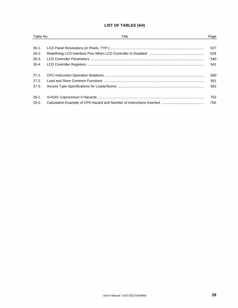
User’s Manual U14272EJ1V0UM00 29
LIST OF TABLES (4/4)
Table No. Title Page
26-1. LCD Panel Resolutions (in Pixels, TYP.) ............................................................................................... 527
26-2. Redefining LCD Interface Pins When LCD Controller Is Disabled ........................................................ 528
26-3. LCD Controller Parameters ................................................................................................................... 540
26-4. LCD Controller Registers ....................................................................................................................... 541
27-1. CPU Instruction Operation Notations ..................................................................................................... 560
27-2. Load and Store Common Functions ...................................................................................................... 561
27-3. Access Type Specifications for Loads/Stores .............................................................................. ......... 562
29-1. VR4181 Coprocessor 0 Hazards ............................................................................................................ 752
29-2. Calculation Example of CP0 Hazard and Number of Instructions Inserted ........................................... 755

User’s Manual U14272EJ1V0UM0030
[MEMO]
User’s Manual U14272EJ1V0UM00 31
CHAPTER 1 INTRODUCTION
This chapter describes the outline of the VR4181 (µ PD30181), which is a 64-bit microprocessor.
1.1 Features
The VR4181, which is a high-performance 64-bit microprocessor employing the RISC (reduced instruction set
computer) architecture developed by MIPSTM, is one of the VR-Series microprocessor products manufactured by
NEC.
The VR4181 contains the VR4110TM CPU core of ultra-low-power consumption with cache memory, high-speed
product-sum operation unit, and memory management unit. It also has interface units for peripheral circuits such as
LCD controller, CompactFlash controller, DMA controller, keyboard interface, serial interface, IrDA interface, touch
panel interface, real-time clock, A/D converter and D/A converter required for the battery-driven portable information
equipment. The features of the VR4181 are described below.
• Employs 0.25 µ m process
• 64-bit RISC VR4110 CPU core with pipeline clock up to 66 MHz (operation in 32-bit mode is available)
• Optimized 5-stage pipeline
• On-chip instruction and data caches with 4 KB each in size
• Write-back cache for reducing store operation that use the system bus
• 32-bit physical address space and 40-bit virtual address space, and 32 double-entry TLB
• Instruction set: MIPS III (with the FPU, LL and SC instructions left out) and MIPS16
• Supports MADD16 and DMADD16 instructions for executing a multiply-and-accumulate operation of 16-bit data
x 16-bit data + 64-bit data within one clock cycle
• Effective power management features, which include four operating modes, Fullspeed, Standby, Suspend and
Hibernate mode
• On-chip PLL and clock generator
• DRAM interface supporting 16-bit width SDRAM and EDO DRAM
• Ordinary ROM/PageROM/flash memory interface
• UMA based LCD controller
• 4-channel DMA controller
• RTC unit including 3-channel timers and counters
• Two UART-compatible serial interfaces and one clocked serial interface
• IrDA(SIR) interface
• Keyboard scan interface supporting 8 x 8 key matrix
• X-Y auto-scan touch panel interface
• CompactFlash interface compatible with ExCA
• A/D and D/A converters
• Includes ISA-subset bus
• Supply voltage: 2.5 V for CPU core, 3.3 V for I/O
• Package: 160-pin LQFP
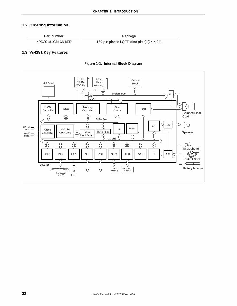
CHAPTER 1 INTRODUCTION
User’s Manual U14272EJ1V0UM0032
1.2 Ordering Information
Part number Package
µ PD30181GM-66-8ED 160-pin plastic LQFP (fine pitch) (24 × 24)
1.3 VR4181 Key Features
Figure 1-1. Internal Block Diagram
LCD Panel
32.768kHz
18.432MHz
EDO DRAM/SDRAM
ModemBlock
ROM/Flash
memory
LCDController
ClockGenerator
VR4110CPU Core MBA
Host BridgeISA Bridge
PMU
PIUSIU1SIU2
IRModule
RS-232-CDriver
GIULED
LED
VR4181
ICU
RTC
Speaker
Microphone
Touch Panel
Battery Monitor
CompactFlashCard
BusControl
MemoryController ECUDCU
BufBuf
AIU D/A
CSIKIU A/DDSU
Keyboard(8 x 8)
ISA Bus
MBA Bus
System Bus
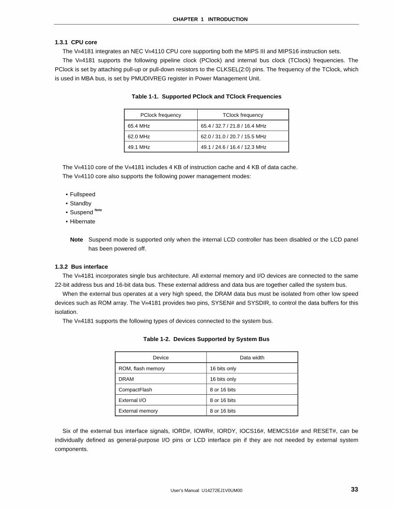
CHAPTER 1 INTRODUCTION
User’s Manual U14272EJ1V0UM00 33
1.3.1 CPU core
The VR4181 integrates an NEC VR4110 CPU core supporting both the MIPS III and MIPS16 instruction sets.
The VR4181 supports the following pipeline clock (PClock) and internal bus clock (TClock) frequencies. The
PClock is set by attaching pull-up or pull-down resistors to the CLKSEL(2:0) pins. The frequency of the TClock, which
is used in MBA bus, is set by PMUDIVREG register in Power Management Unit.
Table 1-1. Supported PClock and TClock Frequencies
PClock frequency TClock frequency
65.4 MHz 65.4 / 32.7 / 21.8 / 16.4 MHz
62.0 MHz 62.0 / 31.0 / 20.7 / 15.5 MHz
49.1 MHz 49.1 / 24.6 / 16.4 / 12.3 MHz
The VR4110 core of the VR4181 includes 4 KB of instruction cache and 4 KB of data cache.
The VR4110 core also supports the following power management modes:
• Fullspeed
• Standby
• Suspend Note
• Hibernate
Note Suspend mode is supported only when the internal LCD controller has been disabled or the LCD panel
has been powered off.
1.3.2 Bus interface
The VR4181 incorporates single bus architecture. All external memory and I/O devices are connected to the same
22-bit address bus and 16-bit data bus. These external address and data bus are together called the system bus.
When the external bus operates at a very high speed, the DRAM data bus must be isolated from other low speed
devices such as ROM array. The VR4181 provides two pins, SYSEN# and SYSDIR, to control the data buffers for this
isolation.
The VR4181 supports the following types of devices connected to the system bus.
Table 1-2. Devices Supported by System Bus
Device Data width
ROM, flash memory 16 bits only
DRAM 16 bits only
CompactFlash 8 or 16 bits
External I/O 8 or 16 bits
External memory 8 or 16 bits
Six of the external bus interface signals, IORD#, IOWR#, IORDY, IOCS16#, MEMCS16# and RESET#, can be
individually defined as general-purpose I/O pins or LCD interface pin if they are not needed by external system
components.
CHAPTER 1 INTRODUCTION
User’s Manual U14272EJ1V0UM0034
1.3.3 Memory interface
The VR4181 provides control for both ROM/flash memory and DRAM. Up to four 16-bit ROM/flash memory banks
may be supported utilizing either 32-Mbit or 64-Mbit single cycle or page mode devices. Bank mixing is not supported
for ROM/flash memory. When a system implements less than the maximum 4 banks of ROM/flash memory, unused
ROM chip select pins can be defined as general-purpose I/O pins.
The VR4181 also supports up to 2 banks of 1M x 16 or 4M x 16 EDO-type DRAM at bus frequencies of up to 66
MHz. When both banks are EDO-type DRAM, bank mixing is supported.
1.3.4 DMA controller (DCU)
The VR4181 provides a 4-channel DMA controller to support internal DMA transfers. The 4 channels are allocated
as follows:
• Channel 1 - Audio input
• Channel 2 - Audio output
• Channel 3, 4 - Reserved
1.3.5 Interrupt controller (ICU)
The VR4181 provides an interrupt controller which combines all interrupt request sources into one of the VR4110
core interrupt inputs - NMI and Int(3:0). The interrupt controller also provides interrupt request status reporting.
1.3.6 Real-time clock
The VR4181 includes a real-time clock (RTC), which allows time keeping based on the 32.768 kHz clock as a
source. The RTC operates as long as the VR4181 remains powered.
1.3.7 Audio output (D/A converter)
The VR4181 provides a 1-channel 10-bit D/A converter for generating audio output.
1.3.8 Touch panel interface and audio input (A/D converter)
The VR4181 provides an 8-channel 10-bit A/D converter for interfacing to a touch panel, an external microphone,
and other types of analog input.
1.3.9 CompactFlash interface (ECU)
The VR4181 provides an ExCA-compatible bus controller supporting a single CompactFlash slot. This interface is
shared with the keyboard interface logic and must be disabled when an 8 x 8 key matrix is connected to the VR4181.
1.3.10 Primary serial interface (SIU1)
The VR4181 provides a 16550 UART for implementing an RS-232-C type serial interface. When the serial
interface is not needed, each of the 7 serial interface pins can be individually redefined as general-purpose I/O pins.
1.3.11 Secondary serial interface (SIU2)
The secondary serial interface is also based on a 16550 UART but only reserves 2 pins for the interface. The
secondary serial interface can be configured in one of the following modes:
• Simple 2-wire serial interface using TxD2 and RxD2
• SIR-type IrDA interface using IRDIN and IRDOUT
• Full RS-232-C compatible interface using TxD2, RxD2 and 5 GPIO pins
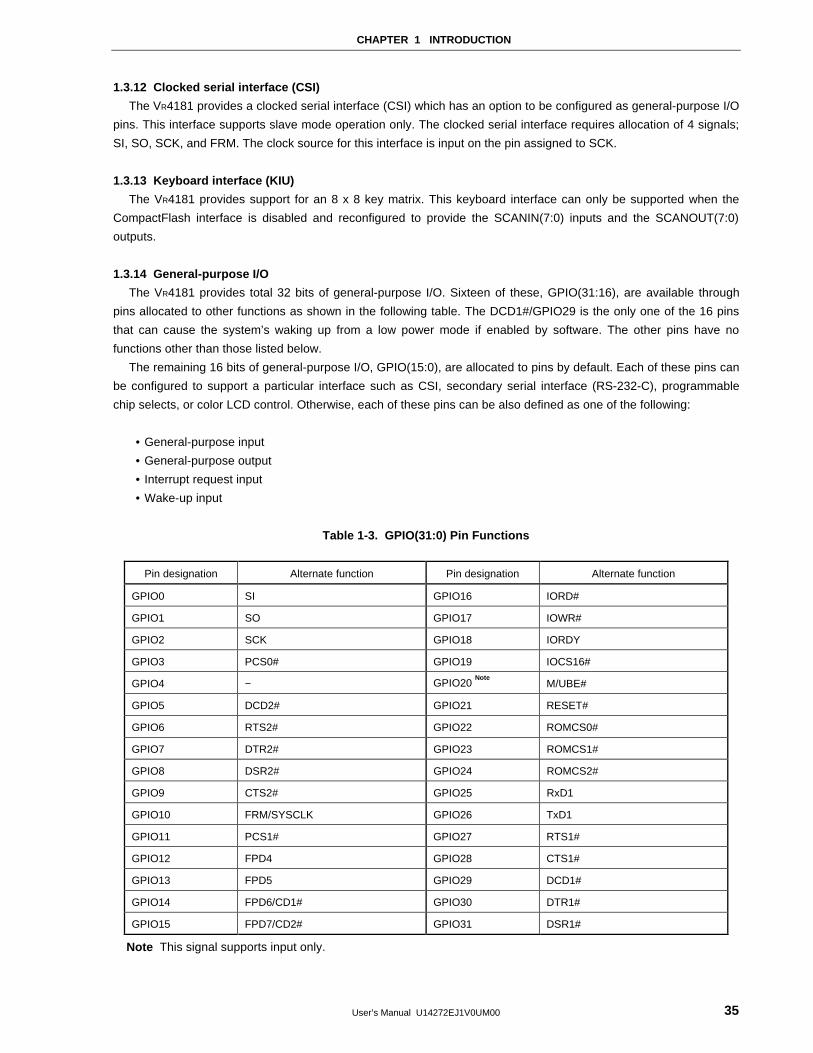
CHAPTER 1 INTRODUCTION
User’s Manual U14272EJ1V0UM00 35
1.3.12 Clocked serial interface (CSI)
The VR4181 provides a clocked serial interface (CSI) which has an option to be configured as general-purpose I/O
pins. This interface supports slave mode operation only. The clocked serial interface requires allocation of 4 signals;
SI, SO, SCK, and FRM. The clock source for this interface is input on the pin assigned to SCK.
1.3.13 Keyboard interface (KIU)
The VR4181 provides support for an 8 x 8 key matrix. This keyboard interface can only be supported when the
CompactFlash interface is disabled and reconfigured to provide the SCANIN(7:0) inputs and the SCANOUT(7:0)
outputs.
1.3.14 General-purpose I/O
The VR4181 provides total 32 bits of general-purpose I/O. Sixteen of these, GPIO(31:16), are available through
pins allocated to other functions as shown in the following table. The DCD1#/GPIO29 is the only one of the 16 pins
that can cause the system’s waking up from a low power mode if enabled by software. The other pins have no
functions other than those listed below.
The remaining 16 bits of general-purpose I/O, GPIO(15:0), are allocated to pins by default. Each of these pins can
be configured to support a particular interface such as CSI, secondary serial interface (RS-232-C), programmable
chip selects, or color LCD control. Otherwise, each of these pins can be also defined as one of the following:
• General-purpose input
• General-purpose output
• Interrupt request input
• Wake-up input
Table 1-3. GPIO(31:0) Pin Functions
Pin designation Alternate function Pin designation Alternate function
GPIO0 SI GPIO16 IORD#
GPIO1 SO GPIO17 IOWR#
GPIO2 SCK GPIO18 IORDY
GPIO3 PCS0# GPIO19 IOCS16#
GPIO4 − GPIO20 Note
M/UBE#
GPIO5 DCD2# GPIO21 RESET#
GPIO6 RTS2# GPIO22 ROMCS0#
GPIO7 DTR2# GPIO23 ROMCS1#
GPIO8 DSR2# GPIO24 ROMCS2#
GPIO9 CTS2# GPIO25 RxD1
GPIO10 FRM/SYSCLK GPIO26 TxD1
GPIO11 PCS1# GPIO27 RTS1#
GPIO12 FPD4 GPIO28 CTS1#
GPIO13 FPD5 GPIO29 DCD1#
GPIO14 FPD6/CD1# GPIO30 DTR1#
GPIO15 FPD7/CD2# GPIO31 DSR1#
Note This signal supports input only.
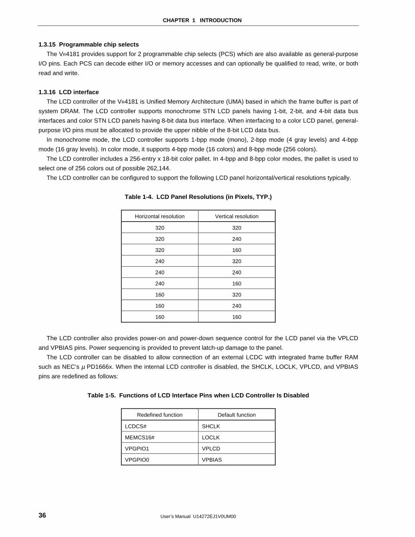
CHAPTER 1 INTRODUCTION
User’s Manual U14272EJ1V0UM0036
1.3.15 Programmable chip selects
The VR4181 provides support for 2 programmable chip selects (PCS) which are also available as general-purpose
I/O pins. Each PCS can decode either I/O or memory accesses and can optionally be qualified to read, write, or both
read and write.
1.3.16 LCD interface
The LCD controller of the VR4181 is Unified Memory Architecture (UMA) based in which the frame buffer is part of
system DRAM. The LCD controller supports monochrome STN LCD panels having 1-bit, 2-bit, and 4-bit data bus
interfaces and color STN LCD panels having 8-bit data bus interface. When interfacing to a color LCD panel, general-
purpose I/O pins must be allocated to provide the upper nibble of the 8-bit LCD data bus.
In monochrome mode, the LCD controller supports 1-bpp mode (mono), 2-bpp mode (4 gray levels) and 4-bpp
mode (16 gray levels). In color mode, it supports 4-bpp mode (16 colors) and 8-bpp mode (256 colors).
The LCD controller includes a 256-entry x 18-bit color pallet. In 4-bpp and 8-bpp color modes, the pallet is used to
select one of 256 colors out of possible 262,144.
The LCD controller can be configured to support the following LCD panel horizontal/vertical resolutions typically.
Table 1-4. LCD Panel Resolutions (in Pixels, TYP.)
Horizontal resolution Vertical resolution
320 320
320 240
320 160
240 320
240 240
240 160
160 320
160 240
160 160
The LCD controller also provides power-on and power-down sequence control for the LCD panel via the VPLCD
and VPBIAS pins. Power sequencing is provided to prevent latch-up damage to the panel.
The LCD controller can be disabled to allow connection of an external LCDC with integrated frame buffer RAM
such as NEC’s µ PD1666x. When the internal LCD controller is disabled, the SHCLK, LOCLK, VPLCD, and VPBIAS
pins are redefined as follows:
Table 1-5. Functions of LCD Interface Pins when LCD Controller Is Disabled
Redefined function Default function
LCDCS# SHCLK
MEMCS16# LOCLK
VPGPIO1 VPLCD
VPGPIO0 VPBIAS
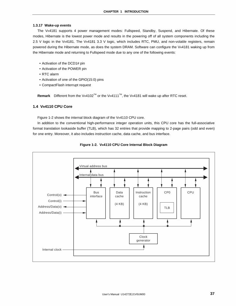
CHAPTER 1 INTRODUCTION
User’s Manual U14272EJ1V0UM00 37
1.3.17 Wake-up events
The VR4181 supports 4 power management modes: Fullspeed, Standby, Suspend, and Hibernate. Of these
modes, Hibernate is the lowest power mode and results in the powering off of all system components including the
2.5 V logic in the VR4181. The VR4181 3.3 V logic, which includes RTC, PMU, and non-volatile registers, remain
powered during the Hibernate mode, as does the system DRAM. Software can configure the VR4181 waking up from
the Hibernate mode and returning to Fullspeed mode due to any one of the following events:
• Activation of the DCD1# pin
• Activation of the POWER pin
• RTC alarm
• Activation of one of the GPIO(15:0) pins
• CompactFlash interrupt request
Remark Different from the VR4102TM or the VR4111TM, the VR4181 will wake up after RTC reset.
1.4 VR4110 CPU Core
Figure 1-2 shows the internal block diagram of the VR4110 CPU core.
In addition to the conventional high-performance integer operation units, this CPU core has the full-associative
format translation lookaside buffer (TLB), which has 32 entries that provide mapping to 2-page pairs (odd and even)
for one entry. Moreover, it also includes instruction cache, data cache, and bus interface.
Figure 1-2. V R4110 CPU Core Internal Block Diagram
TLB
Virtual address bus
Internal data bus
Businterface
Datacache
(4 KB)
Instructioncache
(4 KB)
Clockgenerator
CP0 CPUControl(o)
Control(i)
Address/Data(o)
Address/Data(i)
Internal clock
CHAPTER 1 INTRODUCTION
User’s Manual U14272EJ1V0UM0038
(1) CPU
The CPU has hardware resources to process an integer instruction. They are the 64-bit register file, 64-bit
integer data path, and multiply-and-accumulate operation unit.
(2) Coprocessor 0 (CP0)
The CP0 incorporates a memory management unit (MMU) and exception handling function. MMU checks
whether there is an access between different memory segments (user, supervisor, and kernel) by executing
address conversion. The translation lookaside buffer (TLB) converts virtual addresses to physical addresses.
(3) Instruction cache
The instruction cache employs direct mapping, virtual index, and physical tag. Its capacity is 4 KB.
(4) Data cache
The data cache employs direct mapping, virtual index, physical tag, and write back. Its capacity is 4 KB.
(5) CPU bus interface
The CPU bus interface controls data transmission/reception between the VR4110 core and the MBA Host Bridge.
This interface consists of two 32-bit multiplexed address/data buses (one is for input, and another is for output),
clock signal, and control signals such as interrupt requests.
(6) Clock generator
The following clock inputs are oscillated and supplied to internal units.
• 32.768 kHz clock for RTC unit
Crystal resonator input oscillated via an internal oscillator and supplied to the RTC unit.
• 18.432 MHz clock for serial interface and the VR4181’s reference operating clock
Crystal resonator input oscillated via an internal oscillator, and then multiplied by phase-locked loop (PLL) to
generate a pipeline clock (PClock). The internal bus clock (TClock) is generated from PClock and supplied to
peripheral units.
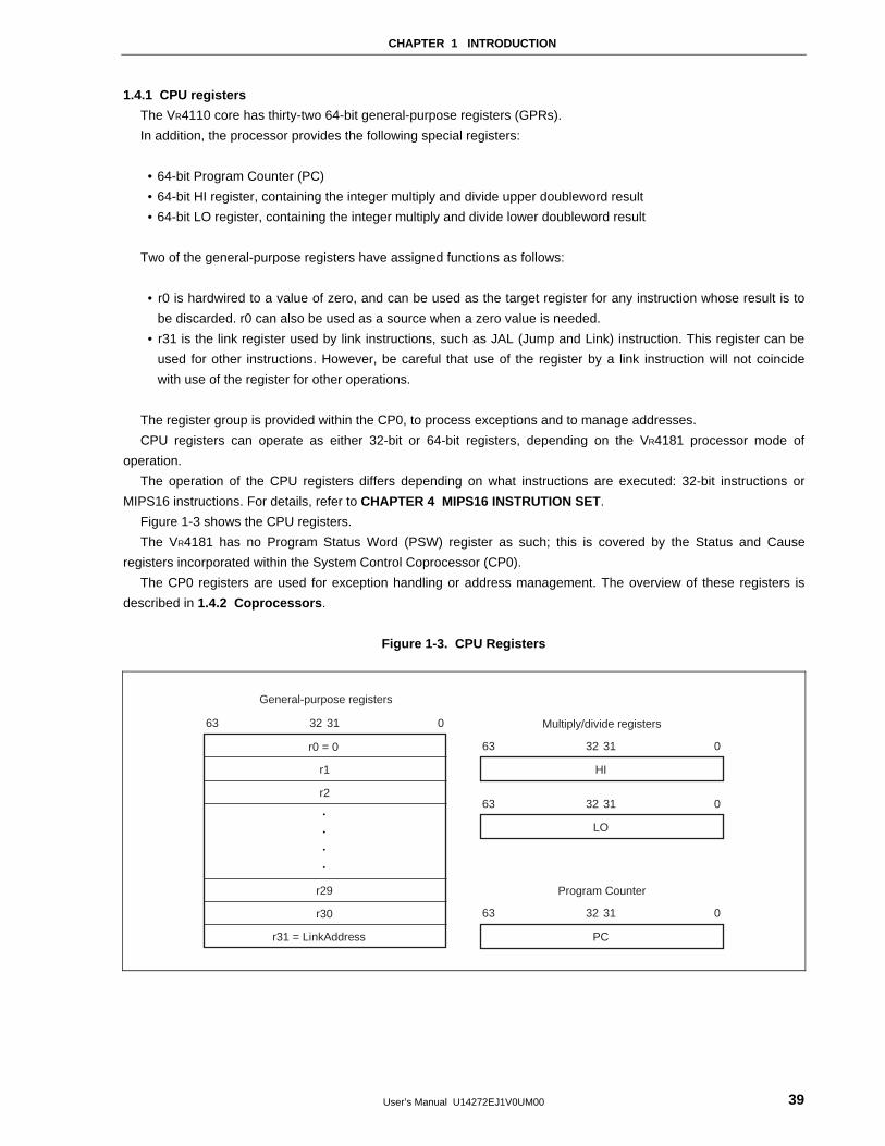
CHAPTER 1 INTRODUCTION
User’s Manual U14272EJ1V0UM00 39
1.4.1 CPU registers
The VR4110 core has thirty-two 64-bit general-purpose registers (GPRs).
In addition, the processor provides the following special registers:
• 64-bit Program Counter (PC)
• 64-bit HI register, containing the integer multiply and divide upper doubleword result
• 64-bit LO register, containing the integer multiply and divide lower doubleword result
Two of the general-purpose registers have assigned functions as follows:
• r0 is hardwired to a value of zero, and can be used as the target register for any instruction whose result is to
be discarded. r0 can also be used as a source when a zero value is needed.
• r31 is the link register used by link instructions, such as JAL (Jump and Link) instruction. This register can be
used for other instructions. However, be careful that use of the register by a link instruction will not coincide
with use of the register for other operations.
The register group is provided within the CP0, to process exceptions and to manage addresses.
CPU registers can operate as either 32-bit or 64-bit registers, depending on the VR4181 processor mode of
operation.
The operation of the CPU registers differs depending on what instructions are executed: 32-bit instructions or
MIPS16 instructions. For details, refer to CHAPTER 4 MIPS16 INSTRUTION SET.
Figure 1-3 shows the CPU registers.
The VR4181 has no Program Status Word (PSW) register as such; this is covered by the Status and Cause
registers incorporated within the System Control Coprocessor (CP0).
The CP0 registers are used for exception handling or address management. The overview of these registers is
described in 1.4.2 Coprocessors .
Figure 1-3. CPU Registers
0313263
HI
0313263
LO
0
PC
31
General-purpose registers
Multiply/divide registers
Program Counter
0
32
31
63
3263
r2
r1
r0 = 0
r31 = LinkAddress
r30
r29
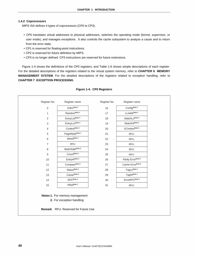
CHAPTER 1 INTRODUCTION
User’s Manual U14272EJ1V0UM0040
1.4.2 Coprocessors
MIPS ISA defines 4 types of coprocessors (CP0 to CP3).
• CP0 translates virtual addresses to physical addresses, switches the operating mode (kernel, supervisor, or
user mode), and manages exceptions. It also controls the cache subsystem to analyze a cause and to return
from the error state.
• CP1 is reserved for floating-point instructions.
• CP2 is reserved for future definition by MIPS.
• CP3 is no longer defined. CP3 instructions are reserved for future extensions.
Figure 1-4 shows the definitions of the CP0 registers, and Table 1-6 shows simple descriptions of each register.
For the detailed descriptions of the registers related to the virtual system memory, refer to CHAPTER 6 MEMORY
MANAGEMENT SYSTEM . For the detailed descriptions of the registers related to exception handling, refer to
CHAPTER 7 EXCEPTION PROCESSING.
Figure 1-4. CP0 Registers
0
1
2
3
4
5
6
7
Register name
RandomNote 1
IndexNote 1
EntryLo0Note 1
EntryLo1Note 1
ContextNote 2
PageMaskNote 1
WiredNote 1
RFU
BadVAddrNote 2
CountNote 2
EntryHiNote 1
CompareNote 2
StatusNote 2
CauseNote 2
EPCNote 2
LLAddrNote 1
ConfigNote 1
WatchLoNote 2
WatchHiNote 2
XContextNote 2
Parity ErrorNote 2
Cache ErrorNote 2
TagLoNote 1
TagHiNote 1
ErrorEPCNote 2
PRIdNote 1
Register No. Register nameRegister No.
8
9
10
11
12
13
14
15
16
17
18
19
20
21 RFU
22 RFU
23 RFU
24 RFU
25 RFU
26
27
28
29
30
31 RFU
Notes 1. For memory management
2. For exception handling
Remark RFU: Reserved for Future Use
CHAPTER 1 INTRODUCTION
User’s Manual U14272EJ1V0UM00 41
Table 1-6. System Control Coprocessor (CP0) Register Definitions
Number Register Description
0 Index Programmable pointer to TLB array
1 Random Pseudo-random pointer to TLB array (read only)
2 EntryLo0 Lower half of TLB entry for even VPN
3 EntryLo1 Lower half of TLB entry for odd VPN
4 Context Pointer to kernel virtual PTE in 32-bit mode
5 PageMask TLB page mask
6 Wired Number of wired TLB entries
7 − Reserved for future use
8 BadVAddr Virtual address where the most recent error occurred
9 Count Timer count
10 EntryHi Higher half of TLB entry (including ASID)
11 Compare Timer compare
12 Status Status indication
13 Cause Cause of last exception
14 EPC Exception Program Counter
15 PRId Processor revision identifier
16 Config Configuration (memory mode system) specification
17 LLAddr Reserved for future use
18 WatchLo Memory reference trap address low bits
19 WatchHi Memory reference trap address high bits
20 XContext Pointer to kernel virtual PTE in 64-bit mode
21 to 25 − Reserved for future use
26 Parity Error Note
Cache parity bits
27 Cache Error Note
Index and status of cache error
28 TagLo Lower half of cache tag
29 TagHi Higher half of cache tag
30 ErrorEPC Error Exception Program Counter
31 − Reserved for future use
Note This register is defined to maintain compatibility with the VR4100TM. This register is not
used in the VR4181 hardware.
CHAPTER 1 INTRODUCTION
User’s Manual U14272EJ1V0UM0042
1.4.3 Floating-point unit (FPU)
The VR4181 does not support the floating-point unit (FPU). Coprocessor Unusable exception will occur if any FPU
instructions are executed. If necessary, FPU instructions should be emulated by software in an exception handler.
1.4.4 CPU core memory management unit
The VR4181 has a 32-bit physical addressing range of 4 GB. However, since it is rare for systems to implement a
physical memory space as large as that memory space, the CPU provides a logical expansion of memory space by
translating addresses composed in the large virtual address space into available physical memory addresses. The
VR4181 supports the following two addressing modes:
• 32-bit mode, in which the virtual address space is divided into 2 GB for user process and 2 GB for the kernel.
• 64-bit mode, in which the virtual address is expanded to 1 tera byte (240 bytes) of user virtual address space.
A detailed description of these address spaces is given in Chapter 6.
1.4.5 Translation lookaside buffer (TLB)
Virtual memory mapping is performed using the translation lookaside buffer (TLB). The TLB converts virtual
addresses to physical addresses. It runs by a full-associative method. It has 32 entries, each mapping a pair of pages
having a variable size (1 KB to 256 KB).
(1) Joint TLB (JTLB)
JTLB holds both an instruction address and data address.
For fast virtual-to-physical address decoding, the VR4181 uses a large, fully associative TLB (joint TLB) that
translates 64 virtual pages to their corresponding physical addresses. The TLB is organized as 32 pairs of even-
odd entries, and maps a virtual address and address space identifier (ASID) into the 4-GB physical address
space.
The page size can be configured, on a per-entry basis, to map a page size of 1 KB to 256 KB. A CP0 register
stores the size of the page to be mapped, and that size is entered into the TLB when a new entry is written.
Thus, operating systems can provide special purpose maps; for example, a typical frame buffer can be memory-
mapped using only one TLB entry.
Translating a virtual address to a physical address begins by comparing the virtual address from the processor
with the physical addresses in the TLB; there is a match when the virtual page number (VPN) of the address is
the same as the VPN field of the entry, and either the Global (G) bit of the TLB entry is set, or the ASID field of
the virtual address is the same as the ASID field of the TLB entry.
This match is referred to as a TLB hit. If there is no match, a TLB Miss exception is taken by the processor and
software is allowed to refill the TLB from a page table of virtual/physical addresses in memory.
1.4.6 Operating mode
The VR4181 has three operating modes:
• User mode
• Supervisor mode
• Kernel mode
The manner in which memory addresses are translated or mapped depends on these operating modes. Refer to
CHAPTER 6 MEMORY MANAGEMENT SYSTEM for details.
CHAPTER 1 INTRODUCTION
User’s Manual U14272EJ1V0UM00 43
1.4.7 Cache
The VR4181 chip incorporates instruction and data caches, which are independent of each other. This
configuration enables high-performance pipeline operations. Both caches have a 64-bit data bus, enabling a one-
clock access. These buses can be accessed in parallel. The instruction cache of the VR4181 has a storage capacity
of 4 KB, while the data cache has a capacity of 4 KB.
A detailed description of caches is given in CHAPETE 9 CACHE MEMORY .
1.5 Instruction Pipeline
The VR4181 has a 5-stage instruction pipeline. Under normal circumstances, one instruction is issued each cycle.
A detailed description of pipeline is provided in CHAPTER 5 VR4181 PIPELINE.
1.6 Clock Interface
The VR4181 has the following seven clocks.
• CLKX1, CLKX2 (input)
These are oscillation inputs of 18.432 MHz, and used to generate operation clocks for the CPU core, serial
interface, and other peripheral units.
• RTCX1, RTCX2 (input)
These are oscillation inputs of 32.768 kHz, and used for PMU, RTC, and so on.
• PClock (internal)
This clock is used to control the pipeline in the VR4110 core, and for units relating to the pipeline. This clock is
generated from the clock input of CLKX1 and CLKX2 pins via the PLL. Its frequency is determined by
CLKSEL(2:0) pins.
• MasterOut (internal)
This is a bus clock of the VR4110 core, and used for interrupt control. The contents of the CP0’s Count register
are incremented synchronously with this clock.
• TClock (internal)
This is an operation clock for internal MBA bus and is supplied to the internal MBA modules (memory controller,
LCD controller, and DMA controller). This clock is generated from PClock and its frequency is 1/1,1/2,1/3 or 1/4
of the PClock frequency (It is determined by internal register setting).
• PCLK (internal)
This clock is supplied to the internal ISA peripherals. This clock is generated from TClock (MBA clock) and its
frequency is determined by internal register setting.
• SYSCLK (internal, output)
This clock is used as the external ISA bus clock. It is also supplied to the internal CompactFlash controller. This
clock is generated from PCLK and its frequency is determined by internal register setting.

User’s Manual U14272EJ1V0UM0044
[MEMO]
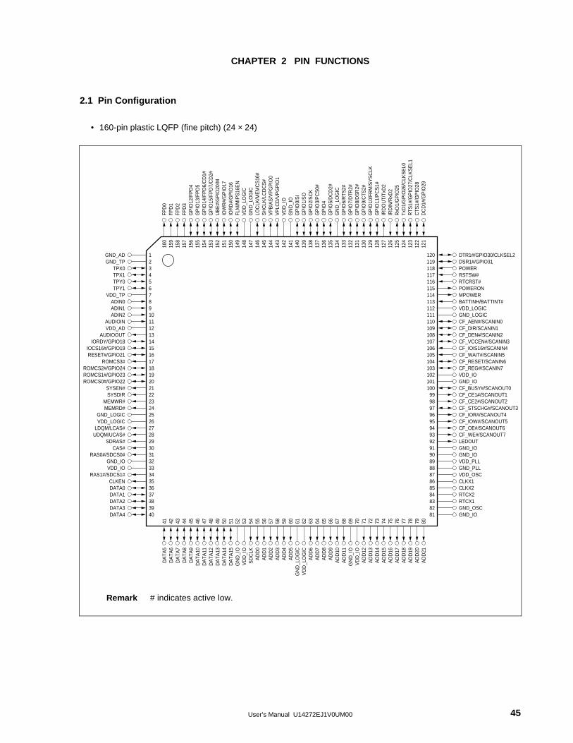
User’s Manual U14272EJ1V0UM00 45
CHAPTER 2 PIN FUNCTIONS
2.1 Pin Configuration
• 160-pin plastic LQFP (fine pitch) (24 × 24)
FPD
0FP
D1
FPD
2FP
D3
GP
IO12
/FP
D4
GP
IO13
/FP
D5
GP
IO14
/FP
D6/
CD
1#G
PIO
15/F
PD
7/C
D2#
UB
E#/
GP
IO20
/MIO
WR
#/G
PIO
17IO
RD
#/G
PIO
16FL
M/M
IPS
16E
NV
DD
_LO
GIC
GN
D_L
OG
ICLO
CLK
/ME
MC
S16
#S
HC
LK/L
CD
CS
#V
PB
IAS
/VP
GP
IO0
VP
LCD
/VP
GP
IO1
VD
D_I
OG
ND
_IO
GP
IO0/
SI
GP
IO1/
SO
GP
IO2/
SC
KG
PIO
3/P
CS
0#G
PIO
4G
PIO
5/D
CD
2#G
ND
_LO
GIC
GP
IO6/
RTS
2#G
PIO
7/D
TR2#
GP
IO8/
DS
R2#
GP
IO9/
CTS
2#G
PIO
10/F
RM
/SY
SC
LKG
PIO
11/P
CS
1#IR
DO
UT/
TxD
2IR
DIN
/RxD
2R
xD1/
GP
IO25
TxD
1/G
PIO
26/C
LKS
EL0
RTS
1#/G
PIO
27/C
LKS
EL1
CTS
1#/G
PIO
28D
CD
1#/G
PIO
29
41 42 43 44 45 46 47 48 49 50 51 52 53 54 55 56 57 58 59 60 61 62 63 64 65 66 67 68 69 70 71 72 73 74 75 76 77 78 79 80
160
159
158
157
156
155
154
153
152
151
150
149
148
147
146
145
144
143
142
141
140
139
138
137
136
135
134
133
132
131
130
129
128
127
126
125
124
123
122
121
DA
TA5
DA
TA6
DA
TA7
DA
TA8
DA
TA9
DA
TA10
DA
TA11
DA
TA12
DA
TA13
DA
TA14
DA
TA15
GN
D_I
OV
DD
_IO
SD
CLK
AD
D0
AD
D1
AD
D2
AD
D3
AD
D4
AD
D5
GN
D_L
OG
ICV
DD
_LO
GIC
AD
D6
AD
D7
AD
D8
AD
D9
AD
D10
AD
D11
GN
D_I
OV
DD
_IO
AD
D12
AD
D13
AD
D14
AD
D15
AD
D16
AD
D17
AD
D18
AD
D19
AD
D20
AD
D21
12345678910111213141516171819202122232425262728293031323334353637383940
DTR1#/GPIO30/CLKSEL2DSR1#/GPIO31POWERRSTSW#RTCRST#POWERONMPOWERBATTINH/BATTINT#VDD_LOGICGND_LOGICCF_AEN#/SCANIN0CF_DIR/SCANIN1CF_DEN#/SCANIN2CF_VCCEN#/SCANIN3CF_IOIS16#/SCANIN4CF_WAIT#/SCANIN5CF_RESET/SCANIN6CF_REG#/SCANIN7VDD_IOGND_IOCF_BUSY#/SCANOUT0CF_CE1#/SCANOUT1CF_CE2#/SCANOUT2CF_STSCHG#/SCANOUT3CF_IOR#/SCANOUT4CF_IOW#/SCANOUT5CF_OE#/SCANOUT6CF_WE#/SCANOUT7LEDOUTGND_IOGND_IOVDD_PLLGND_PLLVDD_OSCCLKX1CLKX2RTCX2RTCX1GND_OSCGND_IO
GND_ADGND_TP
TPX0TPX1TPY0TPY1
VDD_TPADIN0ADIN1ADIN2
AUDIOINVDD_AD
AUDIOOUTIORDY/GPIO18
IOCS16#/GPIO19RESET#/GPIO21
ROMCS3#ROMCS2#/GPIO24ROMCS1#/GPIO23ROMCS0#/GPIO22
SYSEN#SYSDIR
MEMWR#MEMRD#
GND_LOGICVDD_LOGIC
LDQM/LCAS#UDQM/UCAS#
SDRAS#CAS#
RAS0#/SDCS0#GND_IOVDD_IO
RAS1#/SDCS1#CLKENDATA0DATA1DATA2DATA3DATA4
120119118117116115114113112111110109108107106105104103102101100
99989796959493929190898887868584838281
Remark # indicates active low.
CHAPTER 2 PIN FUNCTIONS
User’s Manual U14272EJ1V0UM0046
Pin Identification
ADD(21:0) : Address Bus
ADIN(2:0) : Analog Data Input
AUDIOIN : Audio Input
AUDIOOUT : Audio Output
BATTINH : Battery Inhibit
BATTINT# : Battery Interrupt
CAS# : Column Address Strobe
CD1#, CD2# : Card Detect for CompactFlash
CF_AEN# : Address Enable for CompactFlash Buffer
CF_BUSY# : Ready/Busy/Interrupt Request for CompactFlash
CF_CE(2:1)# : Card Enable for CompactFlash
CF_DEN# : Data Enable for CompactFlash Buffer
CF_DIR : Data Direction for CompactFlash Buffer
CF_IOIS16# : I/O is 16 bits for CompactFlash
CF_IOR# : I/O Read Strobe for CompactFlash
CF_LOW# : I/O Write Strobe for CompactFlash
CF_OE# : Output Enable for CompactFlash
CF_REG# : Register Memory Access for CompactFlash
CF_RESET : Reset for CompactFlash
CF_STSCHG# : Status Change of CompactFlash
CF_VCCEN# : VCC Enable for CompactFlash
CF_WAIT# : Wait Input for CompactFlash
CF_WE# : Write Enable for CompactFlash
CLKEN : Clock Enable for SDRAM
CLKSEL(2:0) : Clock Select
CLKX1, CLKX2 : Clock Input
CTS1#, CTS2# : Clear to Send
DATA(15:0) : Data Bus
DCD1#, DCD2# : Data Carrier Detect
DSR1#, DSR2# : Data Set Ready
DTR1#, DTR2# : Data Terminal Ready
FLM : First Line Clock for LCD
FPD(7:0) : Screen Data of LCD
FRM : Clocked Serial Frame
GND_AD : Ground for A/D and D/A Converter
GND_IO : Ground for I/O
GND_LOGIC : Ground for Logic
GND_OSC : Ground for Oscillator
GND_PLL : Ground for PLL
GND_TP : Ground for Touch Panel
GPIO(31:0) : General Purpose I/O
IOCS16# : I/O 16-bit Bus Sizing
IORD# : I/O Read
IORDY : I/O Ready
IOWR# : I/O Write
IRDIN : IrDA Data Input
IRDOUT : IrDA Data Output
LCAS# : Lower Column Address Strobe
LCDCS# : Chip Select for LCD
LDQM : Lower Byte Enable for SDRAM
LEDOUT : LED Output
LOCLK : Load Clock for LCD
M : LCD Modulation Clock
MEMCS16# : Memory 16-bit Bus Sizing
MEMRD# : Memory Read
MEMWR# : Memory Write
MIPS16EN : MIPS16 Enable
MPOWER : Main Power
PCS(1:0)# : Programmable Chip Select
POWER : Power Switch
POWERON : Power On State
RAS(1:0)# : Row Address Strobe for DRAM
RESET# : Reset Output
ROMCS(3:0)# : Chip Select for ROM
RSTSW# : Reset Switch
RTCRST# : Real-time Clock Reset
RTCX1, RTCX2 : Real-time Clock Input
RTS1#, RTS2# : Request to Send
RxD1,RxD2 : Receive Data
SCANIN(7:0) : Scan Data Input
SCANOUT(7:0) : Scan Data Output
SCK : CSI (Clocked Serial Interface) Clock
SDCLK : Operation Clock for SDRAM
SDCS(1:0)# : Chip Select for SDRAM
SDRAS# : Row Address Strobe for SDRAM
SHCLK : Shift Clock for LCD
SI : Clocked Serial Data Input
SO : Clocked Serial Data Output
SYSCLK : System Clock for System Bus
SYSDIR : System Data Direction
SYSEN# : System Data Enable
TPX(1:0) : Touch Panel Data of X
TPY(1:0) : Touch Panel Data of Y
TxD1, TxD2 : Transmit Data
UBE# : Upper Byte Enable for System Bus
UCAS# : Upper Column Address Strobe for DRAM
UDQM : Upper Byte Enable for SDRAM
VDD_AD : Power Supply for A/D and D/A Converter
VDD_IO : Power Supply for I/O
VDD_LOGIC : Power Supply for Logic
VDD_OSC : Power Supply for Oscillator
VDD_PLL : Power Supply for PLL
VDD_TP : Power Supply for Touch Panel
VPBIAS : Bias Power Control for LCD
VPGPIO(1:0) : General Purpose Output for LCD Panel Power
Control
VPLCD : Logic Power Control for LCD
Remark # indicates active low.
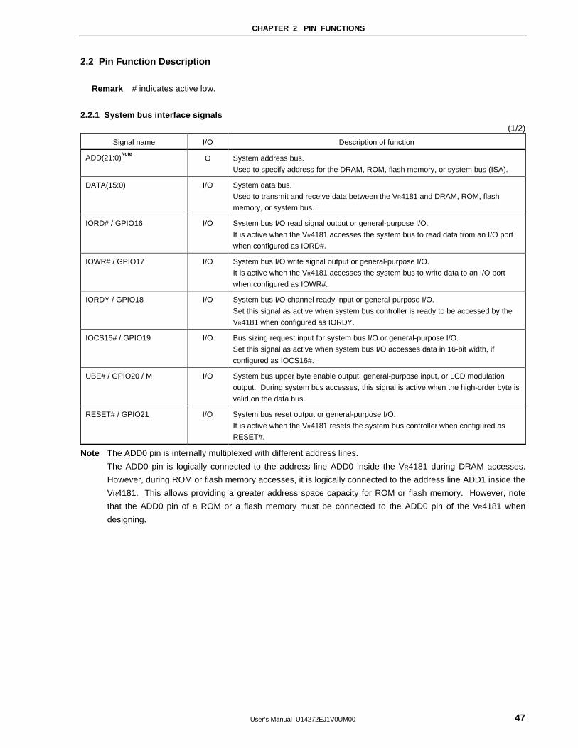
CHAPTER 2 PIN FUNCTIONS
User’s Manual U14272EJ1V0UM00 47
2.2 Pin Function Description
Remark # indicates active low.
2.2.1 System bus interface signals
(1/2)
Signal name I/O Description of function
ADD(21:0)Note
O System address bus.
Used to specify address for the DRAM, ROM, flash memory, or system bus (ISA).
DATA(15:0) I/O System data bus.
Used to transmit and receive data between the VR4181 and DRAM, ROM, flash
memory, or system bus.
IORD# / GPIO16 I/O System bus I/O read signal output or general-purpose I/O.
It is active when the VR4181 accesses the system bus to read data from an I/O port
when configured as IORD#.
IOWR# / GPIO17 I/O System bus I/O write signal output or general-purpose I/O.
It is active when the VR4181 accesses the system bus to write data to an I/O port
when configured as IOWR#.
IORDY / GPIO18 I/O System bus I/O channel ready input or general-purpose I/O.
Set this signal as active when system bus controller is ready to be accessed by the
VR4181 when configured as IORDY.
IOCS16# / GPIO19 I/O Bus sizing request input for system bus I/O or general-purpose I/O.
Set this signal as active when system bus I/O accesses data in 16-bit width, if
configured as IOCS16#.
UBE# / GPIO20 / M I/O System bus upper byte enable output, general-purpose input, or LCD modulation
output. During system bus accesses, this signal is active when the high-order byte is
valid on the data bus.
RESET# / GPIO21 I/O System bus reset output or general-purpose I/O.
It is active when the VR4181 resets the system bus controller when configured as
RESET#.
Note The ADD0 pin is internally multiplexed with different address lines.
The ADD0 pin is logically connected to the address line ADD0 inside the VR4181 during DRAM accesses.
However, during ROM or flash memory accesses, it is logically connected to the address line ADD1 inside the
VR4181. This allows providing a greater address space capacity for ROM or flash memory. However, note
that the ADD0 pin of a ROM or a flash memory must be connected to the ADD0 pin of the VR4181 when
designing.
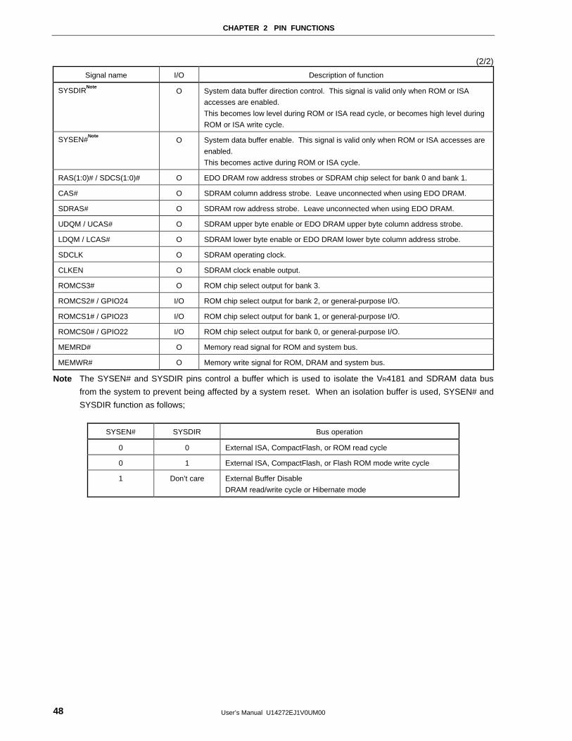
CHAPTER 2 PIN FUNCTIONS
User’s Manual U14272EJ1V0UM0048
(2/2)
Signal name I/O Description of function
SYSDIRNote
O System data buffer direction control. This signal is valid only when ROM or ISA
accesses are enabled.
This becomes low level during ROM or ISA read cycle, or becomes high level during
ROM or ISA write cycle.
SYSEN#Note
O System data buffer enable. This signal is valid only when ROM or ISA accesses are
enabled.
This becomes active during ROM or ISA cycle.
RAS(1:0)# / SDCS(1:0)# O EDO DRAM row address strobes or SDRAM chip select for bank 0 and bank 1.
CAS# O SDRAM column address strobe. Leave unconnected when using EDO DRAM.
SDRAS# O SDRAM row address strobe. Leave unconnected when using EDO DRAM.
UDQM / UCAS# O SDRAM upper byte enable or EDO DRAM upper byte column address strobe.
LDQM / LCAS# O SDRAM lower byte enable or EDO DRAM lower byte column address strobe.
SDCLK O SDRAM operating clock.
CLKEN O SDRAM clock enable output.
ROMCS3# O ROM chip select output for bank 3.
ROMCS2# / GPIO24 I/O ROM chip select output for bank 2, or general-purpose I/O.
ROMCS1# / GPIO23 I/O ROM chip select output for bank 1, or general-purpose I/O.
ROMCS0# / GPIO22 I/O ROM chip select output for bank 0, or general-purpose I/O.
MEMRD# O Memory read signal for ROM and system bus.
MEMWR# O Memory write signal for ROM, DRAM and system bus.
Note The SYSEN# and SYSDIR pins control a buffer which is used to isolate the VR4181 and SDRAM data bus
from the system to prevent being affected by a system reset. When an isolation buffer is used, SYSEN# and
SYSDIR function as follows;
SYSEN# SYSDIR Bus operation
0 0 External ISA, CompactFlash, or ROM read cycle
0 1 External ISA, CompactFlash, or Flash ROM mode write cycle
1 Don’t care External Buffer Disable
DRAM read/write cycle or Hibernate mode
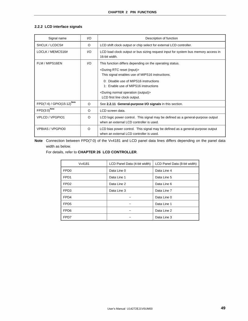
CHAPTER 2 PIN FUNCTIONS
User’s Manual U14272EJ1V0UM00 49
2.2.2 LCD interface signals
Signal name I/O Description of function
SHCLK / LCDCS# O LCD shift clock output or chip select for external LCD controller.
LOCLK / MEMCS16# I/O LCD load clock output or bus sizing request input for system bus memory access in
16-bit width.
FLM / MIPS16EN I/O This function differs depending on the operating status.
<During RTC reset (input)>
This signal enables use of MIPS16 instructions.
0: Disable use of MIPS16 instructions
1: Enable use of MIPS16 instructions
<During normal operation (output)>
LCD first line clock output.
FPD(7:4) / GPIO(15:12)Note
O See 2.2.11 General-purpose I/O signals in this section.
FPD(3:0)Note
O LCD screen data.
VPLCD / VPGPIO1 O LCD logic power control. This signal may be defined as a general-purpose output
when an external LCD controller is used.
VPBIAS / VPGPIO0 O LCD bias power control. This signal may be defined as a general-purpose output
when an external LCD controller is used.
Note Connection between FPD(7:0) of the VR4181 and LCD panel data lines differs depending on the panel data
width as below.
For details, refer to CHAPTER 26 LCD CONTROLLER .
VR4181 LCD Panel Data (4-bit width) LCD Panel Data (8-bit width)
FPD0 Data Line 0 Data Line 4
FPD1 Data Line 1 Data Line 5
FPD2 Data Line 2 Data Line 6
FPD3 Data Line 3 Data Line 7
FPD4 − Data Line 0
FPD5 − Data Line 1
FPD6 − Data Line 2
FPD7 − Data Line 3
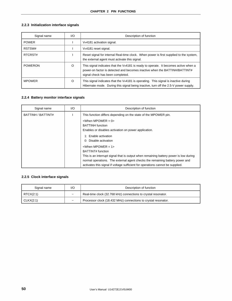
CHAPTER 2 PIN FUNCTIONS
User’s Manual U14272EJ1V0UM0050
2.2.3 Initialization interface signals
Signal name I/O Description of function
POWER I VR4181 activation signal.
RSTSW# I VR4181 reset signal.
RTCRST# I Reset signal for internal Real-time clock. When power is first supplied to the system,
the external agent must activate this signal.
POWERON O This signal indicates that the VR4181 is ready to operate. It becomes active when a
power-on factor is detected and becomes inactive when the BATTINH/BATTINT#
signal check has been completed.
MPOWER O This signal indicates that the VR4181 is operating. This signal is inactive during
Hibernate mode. During this signal being inactive, turn off the 2.5-V power supply.
2.2.4 Battery monitor interface signals
Signal name I/O Description of function
BATTINH / BATTINT# I This function differs depending on the state of the MPOWER pin.
<When MPOWER = 0>
BATTINH function
Enables or disables activation on power application.
1: Enable activation
0: Disable activation
<When MPOWER = 1>
BATTINT# function
This is an interrupt signal that is output when remaining battery power is low during
normal operations. The external agent checks the remaining battery power and
activates this signal if voltage sufficient for operations cannot be supplied.
2.2.5 Clock interface signals
Signal name I/O Description of function
RTCX(2:1) − Real-time clock (32.768 kHz) connections to crystal resonator.
CLKX(2:1) − Processor clock (18.432 MHz) connections to crystal resonator.
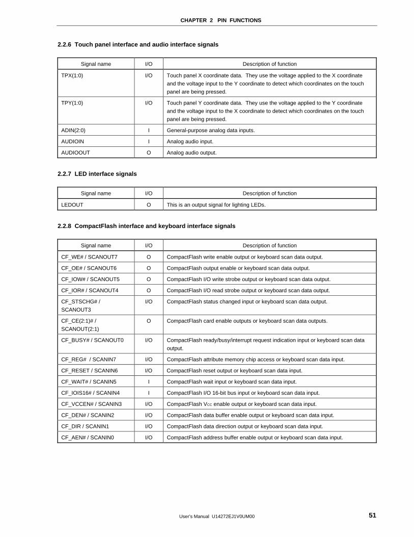
CHAPTER 2 PIN FUNCTIONS
User’s Manual U14272EJ1V0UM00 51
2.2.6 Touch panel interface and audio interface signals
Signal name I/O Description of function
TPX(1:0) I/O Touch panel X coordinate data. They use the voltage applied to the X coordinate
and the voltage input to the Y coordinate to detect which coordinates on the touch
panel are being pressed.
TPY(1:0) I/O Touch panel Y coordinate data. They use the voltage applied to the Y coordinate
and the voltage input to the X coordinate to detect which coordinates on the touch
panel are being pressed.
ADIN(2:0) I General-purpose analog data inputs.
AUDIOIN I Analog audio input.
AUDIOOUT O Analog audio output.
2.2.7 LED interface signals
Signal name I/O Description of function
LEDOUT O This is an output signal for lighting LEDs.
2.2.8 CompactFlash interface and keyboard interface signals
Signal name I/O Description of function
CF_WE# / SCANOUT7 O CompactFlash write enable output or keyboard scan data output.
CF_OE# / SCANOUT6 O CompactFlash output enable or keyboard scan data output.
CF_IOW# / SCANOUT5 O CompactFlash I/O write strobe output or keyboard scan data output.
CF_IOR# / SCANOUT4 O CompactFlash I/O read strobe output or keyboard scan data output.
CF_STSCHG# /
SCANOUT3
I/O CompactFlash status changed input or keyboard scan data output.
CF_CE(2:1)# /
SCANOUT(2:1)
O CompactFlash card enable outputs or keyboard scan data outputs.
CF_BUSY# / SCANOUT0 I/O CompactFlash ready/busy/interrupt request indication input or keyboard scan data
output.
CF_REG# / SCANIN7 I/O CompactFlash attribute memory chip access or keyboard scan data input.
CF_RESET / SCANIN6 I/O CompactFlash reset output or keyboard scan data input.
CF_WAIT# / SCANIN5 I CompactFlash wait input or keyboard scan data input.
CF_IOIS16# / SCANIN4 I CompactFlash I/O 16-bit bus input or keyboard scan data input.
CF_VCCEN# / SCANIN3 I/O CompactFlash VCC enable output or keyboard scan data input.
CF_DEN# / SCANIN2 I/O CompactFlash data buffer enable output or keyboard scan data input.
CF_DIR / SCANIN1 I/O CompactFlash data direction output or keyboard scan data input.
CF_AEN# / SCANIN0 I/O CompactFlash address buffer enable output or keyboard scan data input.
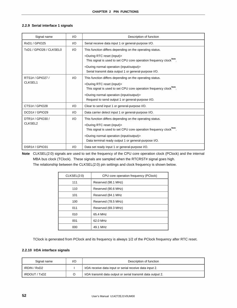
CHAPTER 2 PIN FUNCTIONS
User’s Manual U14272EJ1V0UM0052
2.2.9 Serial interface 1 signals
Signal name I/O Description of function
RxD1 / GPIO25 I/O Serial receive data input 1 or general-purpose I/O.
TxD1 / GPIO26 / CLKSEL0 I/O This function differs depending on the operating status.
<During RTC reset (input)> This signal is used to set CPU core operation frequency clock
Note.
<During normal operation (input/output)>
Serial transmit data output 1 or general-purpose I/O.
RTS1# / GPIO27 /
CLKSEL1
I/O This function differs depending on the operating status.
<During RTC reset (input)> This signal is used to set CPU core operation frequency clock
Note.
<During normal operation (input/output)>
Request to send output 1 or general-purpose I/O.
CTS1# / GPIO28 I/O Clear to send input 1 or general-purpose I/O.
DCD1# / GPIO29 I/O Data carrier detect input 1 or general-purpose I/O.
DTR1# / GPIO30 /
CLKSEL2
I/O This function differs depending on the operating status.
<During RTC reset (input)> This signal is used to set CPU core operation frequency clock
Note.
<During normal operation (input/output)>
Data terminal ready output 1 or general-purpose I/O.
DSR1# / GPIO31 I/O Data set ready input 1 or general-purpose I/O.
Note CLKSEL(2:0) signals are used to set the frequency of the CPU core operation clock (PClock) and the internal
MBA bus clock (TClock). These signals are sampled when the RTCRST# signal goes high.
The relationship between the CLKSEL(2:0) pin settings and clock frequency is shown below.
CLKSEL(2:0) CPU core operation frequency (PClock)
111 Reserved (98.1 MHz)
110 Reserved (90.6 MHz)
101 Reserved (84.1 MHz
100 Reserved (78.5 MHz)
011 Reserved (69.3 MHz)
010 65.4 MHz
001 62.0 MHz
000 49.1 MHz
TClock is generated from PClock and its frequency is always 1/2 of the PClock frequency after RTC reset.
2.2.10 IrDA interface signals
Signal name I/O Description of function
IRDIN / RxD2 I IrDA receive data input or serial receive data input 2.
IRDOUT / TxD2 O IrDA transmit data output or serial transmit data output 2.
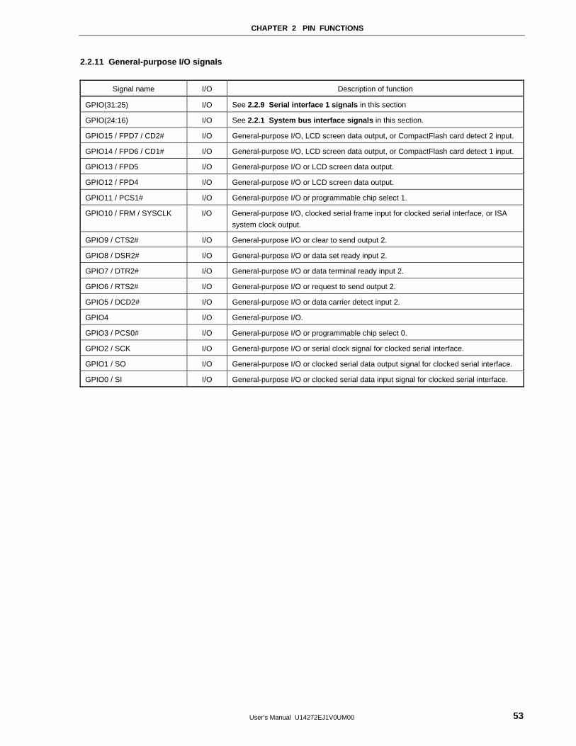
CHAPTER 2 PIN FUNCTIONS
User’s Manual U14272EJ1V0UM00 53
2.2.11 General-purpose I/O signals
Signal name I/O Description of function
GPIO(31:25) I/O See 2.2.9 Serial interface 1 signals in this section
GPIO(24:16) I/O See 2.2.1 System bus interface signals in this section.
GPIO15 / FPD7 / CD2# I/O General-purpose I/O, LCD screen data output, or CompactFlash card detect 2 input.
GPIO14 / FPD6 / CD1# I/O General-purpose I/O, LCD screen data output, or CompactFlash card detect 1 input.
GPIO13 / FPD5 I/O General-purpose I/O or LCD screen data output.
GPIO12 / FPD4 I/O General-purpose I/O or LCD screen data output.
GPIO11 / PCS1# I/O General-purpose I/O or programmable chip select 1.
GPIO10 / FRM / SYSCLK I/O General-purpose I/O, clocked serial frame input for clocked serial interface, or ISA
system clock output.
GPIO9 / CTS2# I/O General-purpose I/O or clear to send output 2.
GPIO8 / DSR2# I/O General-purpose I/O or data set ready input 2.
GPIO7 / DTR2# I/O General-purpose I/O or data terminal ready input 2.
GPIO6 / RTS2# I/O General-purpose I/O or request to send output 2.
GPIO5 / DCD2# I/O General-purpose I/O or data carrier detect input 2.
GPIO4 I/O General-purpose I/O.
GPIO3 / PCS0# I/O General-purpose I/O or programmable chip select 0.
GPIO2 / SCK I/O General-purpose I/O or serial clock signal for clocked serial interface.
GPIO1 / SO I/O General-purpose I/O or clocked serial data output signal for clocked serial interface.
GPIO0 / SI I/O General-purpose I/O or clocked serial data input signal for clocked serial interface.
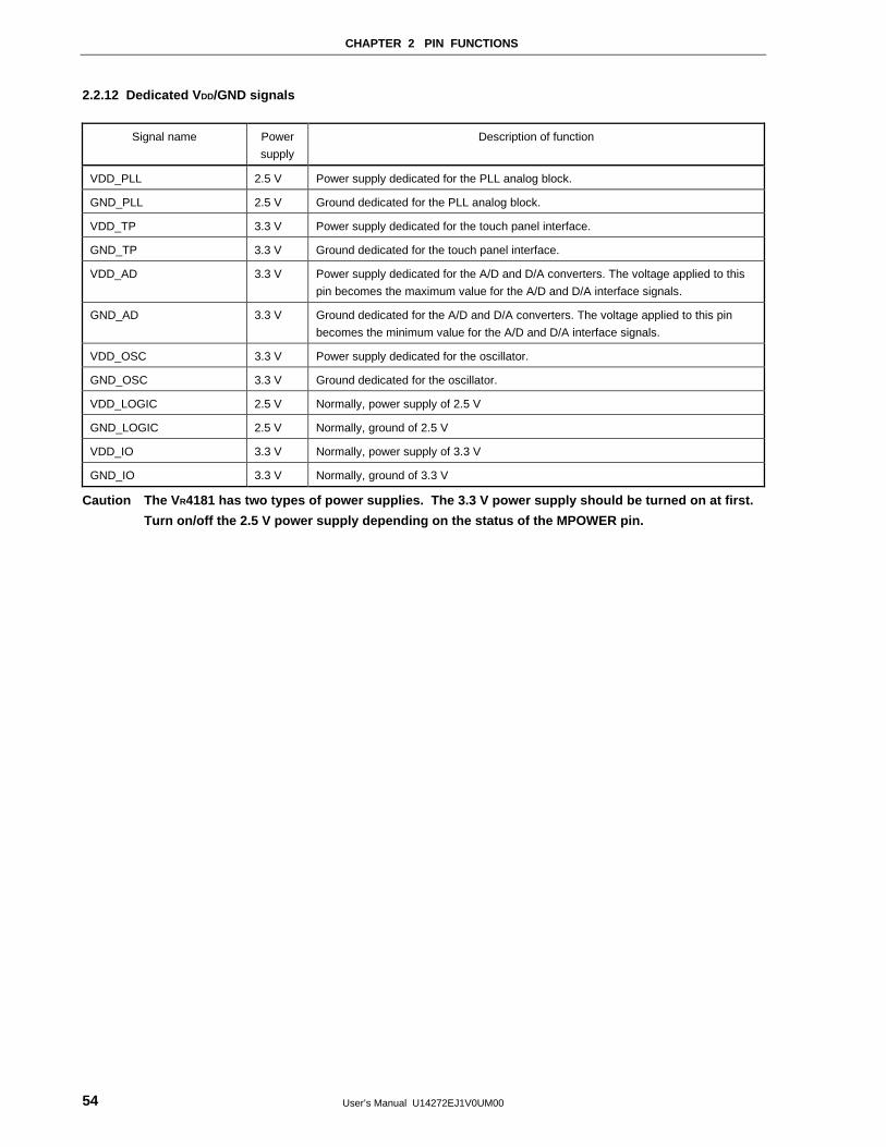
CHAPTER 2 PIN FUNCTIONS
User’s Manual U14272EJ1V0UM0054
2.2.12 Dedicated V DD/GND signals
Signal name Power
supply
Description of function
VDD_PLL 2.5 V Power supply dedicated for the PLL analog block.
GND_PLL 2.5 V Ground dedicated for the PLL analog block.
VDD_TP 3.3 V Power supply dedicated for the touch panel interface.
GND_TP 3.3 V Ground dedicated for the touch panel interface.
VDD_AD 3.3 V Power supply dedicated for the A/D and D/A converters. The voltage applied to this
pin becomes the maximum value for the A/D and D/A interface signals.
GND_AD 3.3 V Ground dedicated for the A/D and D/A converters. The voltage applied to this pin
becomes the minimum value for the A/D and D/A interface signals.
VDD_OSC 3.3 V Power supply dedicated for the oscillator.
GND_OSC 3.3 V Ground dedicated for the oscillator.
VDD_LOGIC 2.5 V Normally, power supply of 2.5 V
GND_LOGIC 2.5 V Normally, ground of 2.5 V
VDD_IO 3.3 V Normally, power supply of 3.3 V
GND_IO 3.3 V Normally, ground of 3.3 V
Caution The V R4181 has two types of power supplies. The 3.3 V power supply should be turned on at first.
Turn on/off the 2.5 V power supply depending on the status of the MPOWER pin.
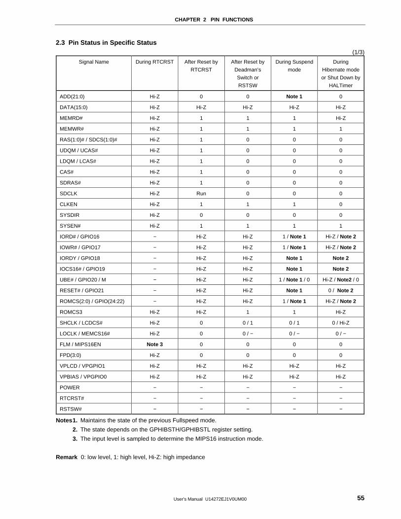
CHAPTER 2 PIN FUNCTIONS
User’s Manual U14272EJ1V0UM00 55
2.3 Pin Status in Specific Status(1/3)
Signal Name During RTCRST After Reset by
RTCRST
After Reset by
Deadman’s
Switch or
RSTSW
During Suspend
mode
During
Hibernate mode
or Shut Down by
HALTimer
ADD(21:0) Hi-Z 0 0 Note 1 0
DATA(15:0) Hi-Z Hi-Z Hi-Z Hi-Z Hi-Z
MEMRD# Hi-Z 1 1 1 Hi-Z
MEMWR# Hi-Z 1 1 1 1
RAS(1:0)# / SDCS(1:0)# Hi-Z 1 0 0 0
UDQM / UCAS# Hi-Z 1 0 0 0
LDQM / LCAS# Hi-Z 1 0 0 0
CAS# Hi-Z 1 0 0 0
SDRAS# Hi-Z 1 0 0 0
SDCLK Hi-Z Run 0 0 0
CLKEN Hi-Z 1 1 1 0
SYSDIR Hi-Z 0 0 0 0
SYSEN# Hi-Z 1 1 1 1
IORD# / GPIO16 − Hi-Z Hi-Z 1 / Note 1 Hi-Z / Note 2
IOWR# / GPIO17 − Hi-Z Hi-Z 1 / Note 1 Hi-Z / Note 2
IORDY / GPIO18 − Hi-Z Hi-Z Note 1 Note 2
IOCS16# / GPIO19 − Hi-Z Hi-Z Note 1 Note 2
UBE# / GPIO20 / M − Hi-Z Hi-Z 1 / Note 1 / 0 Hi-Z / Note2 / 0
RESET# / GPIO21 − Hi-Z Hi-Z Note 1 0 / Note 2
ROMCS(2:0) / GPIO(24:22) − Hi-Z Hi-Z 1 / Note 1 Hi-Z / Note 2
ROMCS3 Hi-Z Hi-Z 1 1 Hi-Z
SHCLK / LCDCS# Hi-Z 0 0 / 1 0 / 1 0 / Hi-Z
LOCLK / MEMCS16# Hi-Z 0 0 / − 0 / − 0 / −
FLM / MIPS16EN Note 3 0 0 0 0
FPD(3:0) Hi-Z 0 0 0 0
VPLCD / VPGPIO1 Hi-Z Hi-Z Hi-Z Hi-Z Hi-Z
VPBIAS / VPGPIO0 Hi-Z Hi-Z Hi-Z Hi-Z Hi-Z
POWER − − − − −
RTCRST# − − − − −
RSTSW# − − − − −
Notes1. Maintains the state of the previous Fullspeed mode.
2. The state depends on the GPHIBSTH/GPHIBSTL register setting.
3. The input level is sampled to determine the MIPS16 instruction mode.
Remark 0: low level, 1: high level, Hi-Z: high impedance
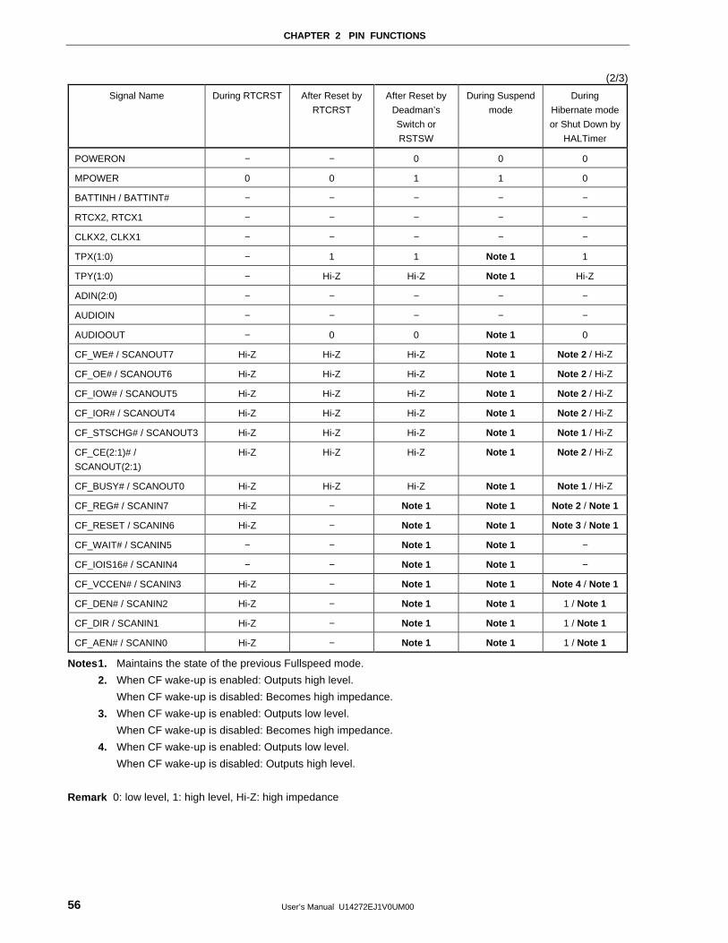
CHAPTER 2 PIN FUNCTIONS
User’s Manual U14272EJ1V0UM0056
(2/3)
Signal Name During RTCRST After Reset by
RTCRST
After Reset by
Deadman’s
Switch or
RSTSW
During Suspend
mode
During
Hibernate mode
or Shut Down by
HALTimer
POWERON − − 0 0 0
MPOWER 0 0 1 1 0
BATTINH / BATTINT# − − − − −
RTCX2, RTCX1 − − − − −
CLKX2, CLKX1 − − − − −
TPX(1:0) − 1 1 Note 1 1
TPY(1:0) − Hi-Z Hi-Z Note 1 Hi-Z
ADIN(2:0) − − − − −
AUDIOIN − − − − −
AUDIOOUT − 0 0 Note 1 0
CF_WE# / SCANOUT7 Hi-Z Hi-Z Hi-Z Note 1 Note 2 / Hi-Z
CF_OE# / SCANOUT6 Hi-Z Hi-Z Hi-Z Note 1 Note 2 / Hi-Z
CF_IOW# / SCANOUT5 Hi-Z Hi-Z Hi-Z Note 1 Note 2 / Hi-Z
CF_IOR# / SCANOUT4 Hi-Z Hi-Z Hi-Z Note 1 Note 2 / Hi-Z
CF_STSCHG# / SCANOUT3 Hi-Z Hi-Z Hi-Z Note 1 Note 1 / Hi-Z
CF_CE(2:1)# /
SCANOUT(2:1)
Hi-Z Hi-Z Hi-Z Note 1 Note 2 / Hi-Z
CF_BUSY# / SCANOUT0 Hi-Z Hi-Z Hi-Z Note 1 Note 1 / Hi-Z
CF_REG# / SCANIN7 Hi-Z − Note 1 Note 1 Note 2 / Note 1
CF_RESET / SCANIN6 Hi-Z − Note 1 Note 1 Note 3 / Note 1
CF_WAIT# / SCANIN5 − − Note 1 Note 1 −
CF_IOIS16# / SCANIN4 − − Note 1 Note 1 −
CF_VCCEN# / SCANIN3 Hi-Z − Note 1 Note 1 Note 4 / Note 1
CF_DEN# / SCANIN2 Hi-Z − Note 1 Note 1 1 / Note 1
CF_DIR / SCANIN1 Hi-Z − Note 1 Note 1 1 / Note 1
CF_AEN# / SCANIN0 Hi-Z − Note 1 Note 1 1 / Note 1
Notes1. Maintains the state of the previous Fullspeed mode.
2. When CF wake-up is enabled: Outputs high level.
When CF wake-up is disabled: Becomes high impedance.
3. When CF wake-up is enabled: Outputs low level.
When CF wake-up is disabled: Becomes high impedance.
4. When CF wake-up is enabled: Outputs low level.
When CF wake-up is disabled: Outputs high level.
Remark 0: low level, 1: high level, Hi-Z: high impedance
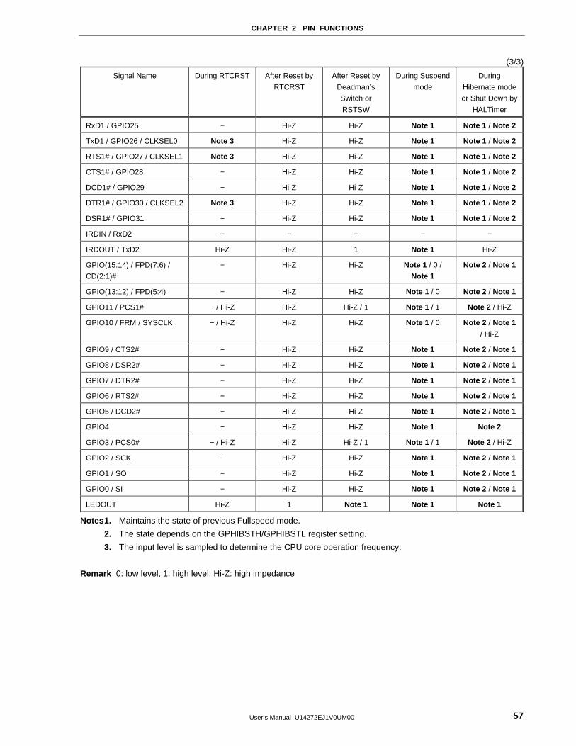
CHAPTER 2 PIN FUNCTIONS
User’s Manual U14272EJ1V0UM00 57
(3/3)
Signal Name During RTCRST After Reset by
RTCRST
After Reset by
Deadman’s
Switch or
RSTSW
During Suspend
mode
During
Hibernate mode
or Shut Down by
HALTimer
RxD1 / GPIO25 − Hi-Z Hi-Z Note 1 Note 1 / Note 2
TxD1 / GPIO26 / CLKSEL0 Note 3 Hi-Z Hi-Z Note 1 Note 1 / Note 2
RTS1# / GPIO27 / CLKSEL1 Note 3 Hi-Z Hi-Z Note 1 Note 1 / Note 2
CTS1# / GPIO28 − Hi-Z Hi-Z Note 1 Note 1 / Note 2
DCD1# / GPIO29 − Hi-Z Hi-Z Note 1 Note 1 / Note 2
DTR1# / GPIO30 / CLKSEL2 Note 3 Hi-Z Hi-Z Note 1 Note 1 / Note 2
DSR1# / GPIO31 − Hi-Z Hi-Z Note 1 Note 1 / Note 2
IRDIN / RxD2 − − − − −
IRDOUT / TxD2 Hi-Z Hi-Z 1 Note 1 Hi-Z
GPIO(15:14) / FPD(7:6) /
CD(2:1)#
− Hi-Z Hi-Z Note 1 / 0 /
Note 1
Note 2 / Note 1
GPIO(13:12) / FPD(5:4) − Hi-Z Hi-Z Note 1 / 0 Note 2 / Note 1
GPIO11 / PCS1# − / Hi-Z Hi-Z Hi-Z / 1 Note 1 / 1 Note 2 / Hi-Z
GPIO10 / FRM / SYSCLK − / Hi-Z Hi-Z Hi-Z Note 1 / 0 Note 2 / Note 1
/ Hi-Z
GPIO9 / CTS2# − Hi-Z Hi-Z Note 1 Note 2 / Note 1
GPIO8 / DSR2# − Hi-Z Hi-Z Note 1 Note 2 / Note 1
GPIO7 / DTR2# − Hi-Z Hi-Z Note 1 Note 2 / Note 1
GPIO6 / RTS2# − Hi-Z Hi-Z Note 1 Note 2 / Note 1
GPIO5 / DCD2# − Hi-Z Hi-Z Note 1 Note 2 / Note 1
GPIO4 − Hi-Z Hi-Z Note 1 Note 2
GPIO3 / PCS0# − / Hi-Z Hi-Z Hi-Z / 1 Note 1 / 1 Note 2 / Hi-Z
GPIO2 / SCK − Hi-Z Hi-Z Note 1 Note 2 / Note 1
GPIO1 / SO − Hi-Z Hi-Z Note 1 Note 2 / Note 1
GPIO0 / SI − Hi-Z Hi-Z Note 1 Note 2 / Note 1
LEDOUT Hi-Z 1 Note 1 Note 1 Note 1
Notes1. Maintains the state of previous Fullspeed mode.
2. The state depends on the GPHIBSTH/GPHIBSTL register setting.
3. The input level is sampled to determine the CPU core operation frequency.
Remark 0: low level, 1: high level, Hi-Z: high impedance

User’s Manual U14272EJ1V0UM0058
[MEMO]
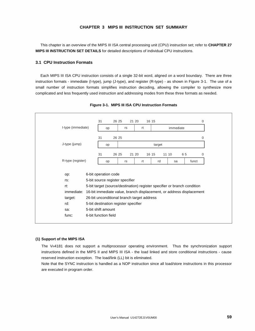
User’s Manual U14272EJ1V0UM00 59
CHAPTER 3 MIPS III INSTRUCTION SET SUMMARY
This chapter is an overview of the MIPS III ISA central processing unit (CPU) instruction set; refer to CHAPTER 27
MIPS III INSTRUCTION SET DETAILS for detailed descriptions of individual CPU instructions.
3.1 CPU Instruction Formats
Each MIPS III ISA CPU instruction consists of a single 32-bit word, aligned on a word boundary. There are three
instruction formats - immediate (I-type), jump (J-type), and register (R-type) - as shown in Figure 3-1. The use of a
small number of instruction formats simplifies instruction decoding, allowing the compiler to synthesize more
complicated and less frequently used instruction and addressing modes from these three formats as needed.
Figure 3-1. MIPS III ISA CPU Instruction Formats
op immediate
015162021252631
op target
0252631
rtrs
op
I-type (immediate)
J-type (jump)
R-type (register)
015162021252631
sard
561011
rtrs funct
op: 6-bit operation code
rs: 5-bit source register specifier
rt: 5-bit target (source/destination) register specifier or branch condition
immediate: 16-bit immediate value, branch displacement, or address displacement
target: 26-bit unconditional branch target address
rd: 5-bit destination register specifier
sa: 5-bit shift amount
func: 6-bit function field
(1) Support of the MIPS ISA
The VR4181 does not support a multiprocessor operating environment. Thus the synchronization support
instructions defined in the MIPS II and MIPS III ISA - the load linked and store conditional instructions - cause
reserved instruction exception. The load/link (LL) bit is eliminated.
Note that the SYNC instruction is handled as a NOP instruction since all load/store instructions in this processor
are executed in program order.
CHAPTER 3 MISP III INSTRUCTION SET SUMMARY
User’s Manual U14272EJ1V0UM0060
3.2 Instruction Classes
The CPU instructions are classified into five classes.
3.2.1 Load and store instructions
Load and store are immediate (I-type) instructions that move data between memory and the general-purpose
registers. The only addressing mode that load and store instructions directly support is base register plus 16-bit
signed immediate offset.
(1) Scheduling a load delay slot
A load instruction that does not allow its result to be used by the instruction immediately following is called a
delayed load instruction. The instruction slot immediately following this delayed load instruction is referred to as
the load delay slot.
In the VR4000 SeriesTM, a load instruction can be followed directly by an instruction that accesses a register that is
loaded by the load instruction. In this case, however, an interlock occurs for a necessary number of cycles. Any
instruction can follow a load instruction, but the load delay slot should be scheduled appropriately for both
performance and compatibility with the VR Series microprocessors. For detail, see CHAPTER 5 VR4181
PIPELINE.
(2) Store delay slot
When a store instruction is writing data to a cache, the data cache is kept busy at the DC and WB stages. If an
instruction (such as load) that follows directly the store instruction accesses the data cache in the DC stage, a
hardware-driven interlock occurs. To overcome this problem, the store delay slot should be scheduled.
Table 3-1. Number of Delay Slot Cycles Necessary for Load and Store Instructions
Instruction Necessary number of PCycles
Load 1
Store 1
(3) Defining access types
Access type indicates the size of a VR4181 processor data item to be loaded or stored, set by the load or store
instruction opcode. Access types and accessed byte are shown in Table 3-2.
Regardless of access type or byte ordering (endianness), the address given specifies the low-order byte in the
addressed field. For a little-endian configuration, the low-order byte is the least-significant byte.
The access type, together with the three low-order bits of the address, define the bytes accessed within the
addressed doubleword (shown in Table 3-2). Only the combinations shown in Table 3-2 are permissible; other
combinations cause address error exceptions.
Tables 3-2 and 3-3 list the ISA-defined load/store instructions and extended-ISA instructions, respectively.
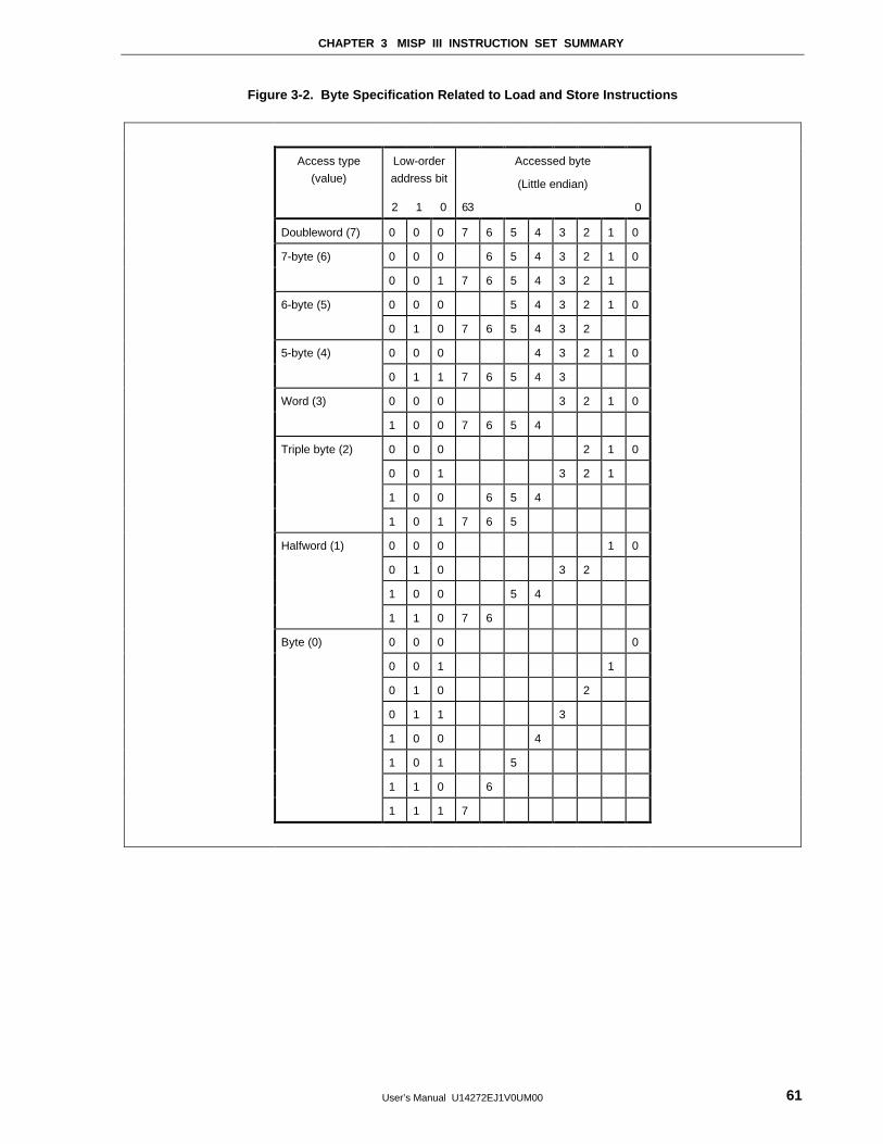
CHAPTER 3 MISP III INSTRUCTION SET SUMMARY
User’s Manual U14272EJ1V0UM00 61
Figure 3-2. Byte Specification Related to Load and Store Instructions
Low-order
address bit
Accessed byte
(Little endian)
Access type
(value)
2 1 0 63 0
Doubleword (7) 0 0 0 7 6 5 4 3 2 1 0
7-byte (6) 0 0 0 6 5 4 3 2 1 0
0 0 1 7 6 5 4 3 2 1
6-byte (5) 0 0 0 5 4 3 2 1 0
0 1 0 7 6 5 4 3 2
5-byte (4) 0 0 0 4 3 2 1 0
0 1 1 7 6 5 4 3
Word (3) 0 0 0 3 2 1 0
1 0 0 7 6 5 4
Triple byte (2) 0 0 0 2 1 0
0 0 1 3 2 1
1 0 0 6 5 4
1 0 1 7 6 5
Halfword (1) 0 0 0 1 0
0 1 0 3 2
1 0 0 5 4
1 1 0 7 6
Byte (0) 0 0 0 0
0 0 1 1
0 1 0 2
0 1 1 3
1 0 0 4
1 0 1 5
1 1 0 6
1 1 1 7
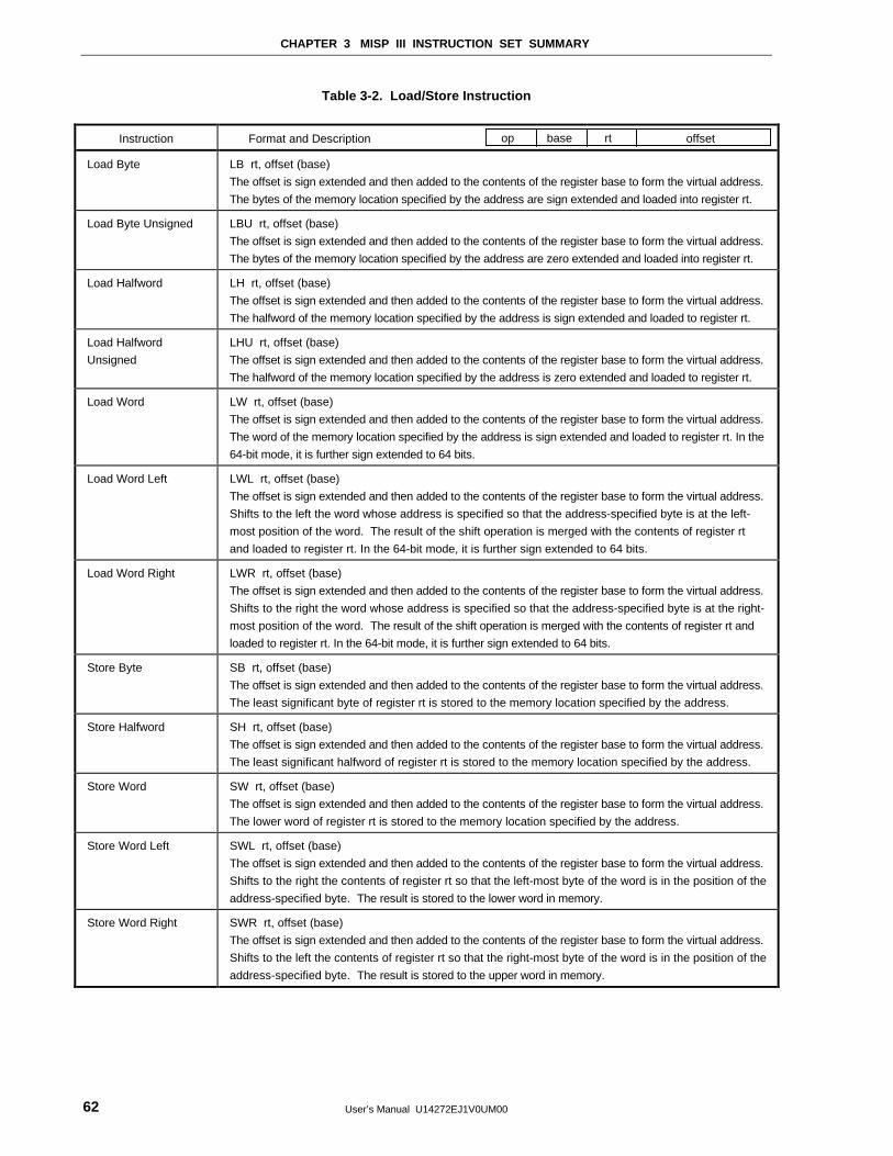
CHAPTER 3 MISP III INSTRUCTION SET SUMMARY
User’s Manual U14272EJ1V0UM0062
Table 3-2. Load/Store Instruction
Instruction Format and Description
Load Byte LB rt, offset (base)
The offset is sign extended and then added to the contents of the register base to form the virtual address.
The bytes of the memory location specified by the address are sign extended and loaded into register rt.
Load Byte Unsigned LBU rt, offset (base)
The offset is sign extended and then added to the contents of the register base to form the virtual address.
The bytes of the memory location specified by the address are zero extended and loaded into register rt.
Load Halfword LH rt, offset (base)
The offset is sign extended and then added to the contents of the register base to form the virtual address.
The halfword of the memory location specified by the address is sign extended and loaded to register rt.
Load Halfword
Unsigned
LHU rt, offset (base)
The offset is sign extended and then added to the contents of the register base to form the virtual address.
The halfword of the memory location specified by the address is zero extended and loaded to register rt.
Load Word LW rt, offset (base)
The offset is sign extended and then added to the contents of the register base to form the virtual address.
The word of the memory location specified by the address is sign extended and loaded to register rt. In the
64-bit mode, it is further sign extended to 64 bits.
Load Word Left LWL rt, offset (base)
The offset is sign extended and then added to the contents of the register base to form the virtual address.
Shifts to the left the word whose address is specified so that the address-specified byte is at the left-
most position of the word. The result of the shift operation is merged with the contents of register rt
and loaded to register rt. In the 64-bit mode, it is further sign extended to 64 bits.
Load Word Right LWR rt, offset (base)
The offset is sign extended and then added to the contents of the register base to form the virtual address.
Shifts to the right the word whose address is specified so that the address-specified byte is at the right-
most position of the word. The result of the shift operation is merged with the contents of register rt and
loaded to register rt. In the 64-bit mode, it is further sign extended to 64 bits.
Store Byte SB rt, offset (base)
The offset is sign extended and then added to the contents of the register base to form the virtual address.
The least significant byte of register rt is stored to the memory location specified by the address.
Store Halfword SH rt, offset (base)
The offset is sign extended and then added to the contents of the register base to form the virtual address.
The least significant halfword of register rt is stored to the memory location specified by the address.
Store Word SW rt, offset (base)
The offset is sign extended and then added to the contents of the register base to form the virtual address.
The lower word of register rt is stored to the memory location specified by the address.
Store Word Left SWL rt, offset (base)
The offset is sign extended and then added to the contents of the register base to form the virtual address.
Shifts to the right the contents of register rt so that the left-most byte of the word is in the position of the
address-specified byte. The result is stored to the lower word in memory.
Store Word Right SWR rt, offset (base)
The offset is sign extended and then added to the contents of the register base to form the virtual address.
Shifts to the left the contents of register rt so that the right-most byte of the word is in the position of the
address-specified byte. The result is stored to the upper word in memory.
op base rt offset
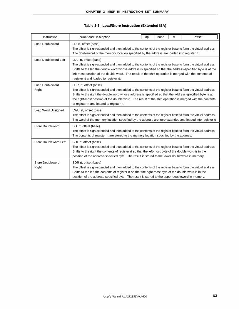
CHAPTER 3 MISP III INSTRUCTION SET SUMMARY
User’s Manual U14272EJ1V0UM00 63
Table 3-3. Load/Store Instruction (Extended ISA)
Instruction Format and Description
Load Doubleword LD rt, offset (base)
The offset is sign extended and then added to the contents of the register base to form the virtual address.
The doubleword of the memory location specified by the address are loaded into register rt.
Load Doubleword Left LDL rt, offset (base)
The offset is sign extended and then added to the contents of the register base to form the virtual address.
Shifts to the left the double word whose address is specified so that the address-specified byte is at the
left-most position of the double word. The result of the shift operation is merged with the contents of
register rt and loaded to register rt.
Load Doubleword
Right
LDR rt, offset (base)
The offset is sign extended and then added to the contents of the register base to form the virtual address.
Shifts to the right the double word whose address is specified so that the address-specified byte is at
the right-most position of the double word. The result of the shift operation is merged with the contents
of register rt and loaded to register rt.
Load Word Unsigned LWU rt, offset (base)
The offset is sign extended and then added to the contents of the register base to form the virtual address.
The word of the memory location specified by the address are zero extended and loaded into register rt
Store Doubleword SD rt, offset (base)
The offset is sign extended and then added to the contents of the register base to form the virtual address.
The contents of register rt are stored to the memory location specified by the address.
Store Doubleword Left SDL rt, offset (base)
The offset is sign extended and then added to the contents of the register base to form the virtual address.
Shifts to the right the contents of register rt so that the left-most byte of the double word is in the
position of the address-specified byte. The result is stored to the lower doubleword in memory.
Store Doubleword
Right
SDR rt, offset (base)
The offset is sign extended and then added to the contents of the register base to form the virtual address.
Shifts to the left the contents of register rt so that the right-most byte of the double word is in the
position of the address-specified byte. The result is stored to the upper doubleword in memory.
op base rt offset
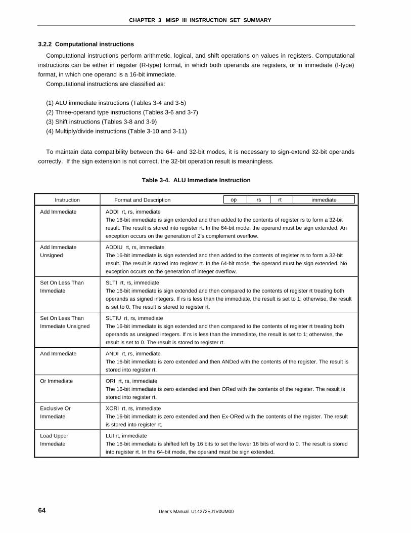
CHAPTER 3 MISP III INSTRUCTION SET SUMMARY
User’s Manual U14272EJ1V0UM0064
3.2.2 Computational instructions
Computational instructions perform arithmetic, logical, and shift operations on values in registers. Computational
instructions can be either in register (R-type) format, in which both operands are registers, or in immediate (I-type)
format, in which one operand is a 16-bit immediate.
Computational instructions are classified as:
(1) ALU immediate instructions (Tables 3-4 and 3-5)
(2) Three-operand type instructions (Tables 3-6 and 3-7)
(3) Shift instructions (Tables 3-8 and 3-9)
(4) Multiply/divide instructions (Table 3-10 and 3-11)
To maintain data compatibility between the 64- and 32-bit modes, it is necessary to sign-extend 32-bit operands
correctly. If the sign extension is not correct, the 32-bit operation result is meaningless.
Table 3-4. ALU Immediate Instruction
Instruction Format and Description
Add Immediate ADDI rt, rs, immediate
The 16-bit immediate is sign extended and then added to the contents of register rs to form a 32-bit
result. The result is stored into register rt. In the 64-bit mode, the operand must be sign extended. An
exception occurs on the generation of 2’s complement overflow.
Add Immediate
Unsigned
ADDIU rt, rs, immediate
The 16-bit immediate is sign extended and then added to the contents of register rs to form a 32-bit
result. The result is stored into register rt. In the 64-bit mode, the operand must be sign extended. No
exception occurs on the generation of integer overflow.
Set On Less Than
Immediate
SLTI rt, rs, immediate
The 16-bit immediate is sign extended and then compared to the contents of register rt treating both
operands as signed integers. If rs is less than the immediate, the result is set to 1; otherwise, the result
is set to 0. The result is stored to register rt.
Set On Less Than
Immediate Unsigned
SLTIU rt, rs, immediate
The 16-bit immediate is sign extended and then compared to the contents of register rt treating both
operands as unsigned integers. If rs is less than the immediate, the result is set to 1; otherwise, the
result is set to 0. The result is stored to register rt.
And Immediate ANDI rt, rs, immediate
The 16-bit immediate is zero extended and then ANDed with the contents of the register. The result is
stored into register rt.
Or Immediate ORI rt, rs, immediate
The 16-bit immediate is zero extended and then ORed with the contents of the register. The result is
stored into register rt.
Exclusive Or
Immediate
XORI rt, rs, immediate
The 16-bit immediate is zero extended and then Ex-ORed with the contents of the register. The result
is stored into register rt.
Load Upper
Immediate
LUI rt, immediate
The 16-bit immediate is shifted left by 16 bits to set the lower 16 bits of word to 0. The result is stored
into register rt. In the 64-bit mode, the operand must be sign extended.
op rs rt immediate
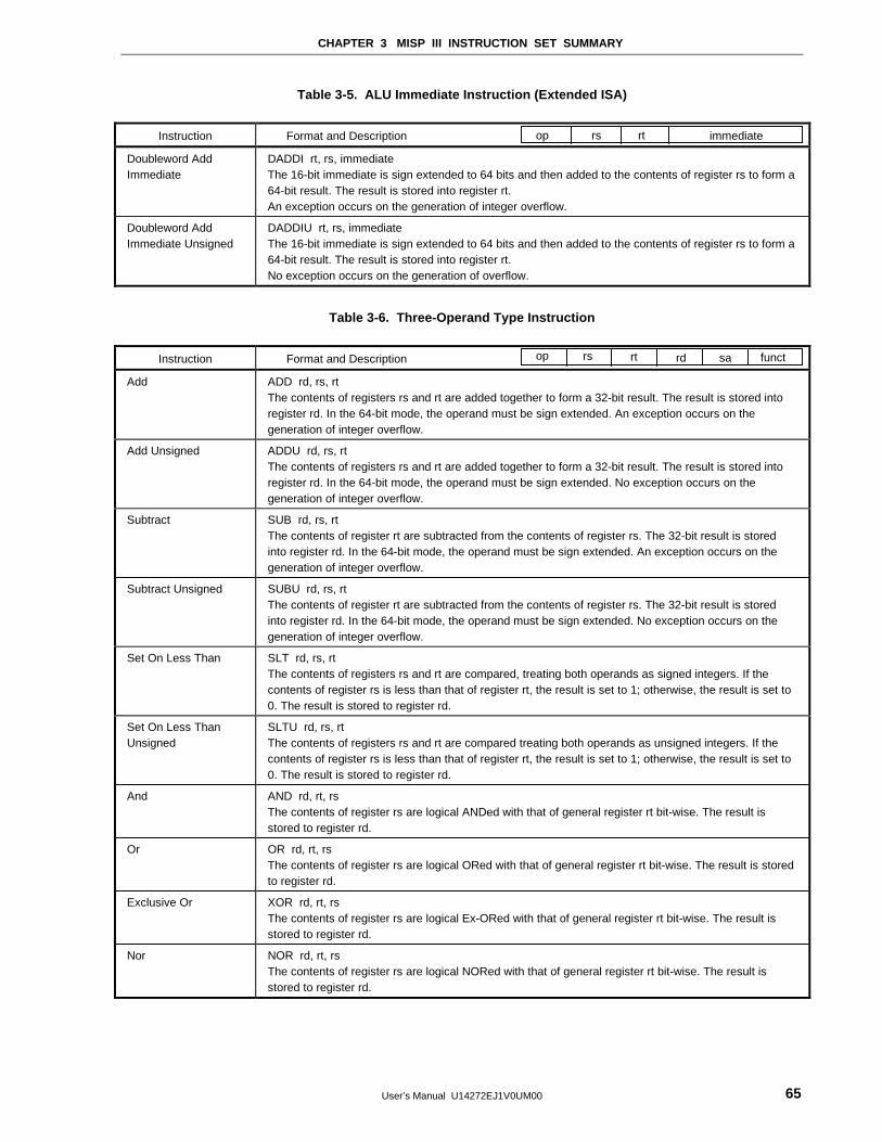
CHAPTER 3 MISP III INSTRUCTION SET SUMMARY
User’s Manual U14272EJ1V0UM00 65
Table 3-5. ALU Immediate Instruction (Extended ISA)
Instruction Format and Description
Doubleword AddImmediate
DADDI rt, rs, immediateThe 16-bit immediate is sign extended to 64 bits and then added to the contents of register rs to form a64-bit result. The result is stored into register rt.An exception occurs on the generation of integer overflow.
Doubleword AddImmediate Unsigned
DADDIU rt, rs, immediateThe 16-bit immediate is sign extended to 64 bits and then added to the contents of register rs to form a64-bit result. The result is stored into register rt.No exception occurs on the generation of overflow.
Table 3-6. Three-Operand Type Instruction
Instruction Format and Description
Add ADD rd, rs, rtThe contents of registers rs and rt are added together to form a 32-bit result. The result is stored intoregister rd. In the 64-bit mode, the operand must be sign extended. An exception occurs on thegeneration of integer overflow.
Add Unsigned ADDU rd, rs, rtThe contents of registers rs and rt are added together to form a 32-bit result. The result is stored intoregister rd. In the 64-bit mode, the operand must be sign extended. No exception occurs on thegeneration of integer overflow.
Subtract SUB rd, rs, rtThe contents of register rt are subtracted from the contents of register rs. The 32-bit result is storedinto register rd. In the 64-bit mode, the operand must be sign extended. An exception occurs on thegeneration of integer overflow.
Subtract Unsigned SUBU rd, rs, rtThe contents of register rt are subtracted from the contents of register rs. The 32-bit result is storedinto register rd. In the 64-bit mode, the operand must be sign extended. No exception occurs on thegeneration of integer overflow.
Set On Less Than SLT rd, rs, rtThe contents of registers rs and rt are compared, treating both operands as signed integers. If thecontents of register rs is less than that of register rt, the result is set to 1; otherwise, the result is set to0. The result is stored to register rd.
Set On Less ThanUnsigned
SLTU rd, rs, rtThe contents of registers rs and rt are compared treating both operands as unsigned integers. If thecontents of register rs is less than that of register rt, the result is set to 1; otherwise, the result is set to0. The result is stored to register rd.
And AND rd, rt, rsThe contents of register rs are logical ANDed with that of general register rt bit-wise. The result isstored to register rd.
Or OR rd, rt, rsThe contents of register rs are logical ORed with that of general register rt bit-wise. The result is storedto register rd.
Exclusive Or XOR rd, rt, rsThe contents of register rs are logical Ex-ORed with that of general register rt bit-wise. The result isstored to register rd.
Nor NOR rd, rt, rsThe contents of register rs are logical NORed with that of general register rt bit-wise. The result isstored to register rd.
op rs rt immediate
op rs rt functrd sa
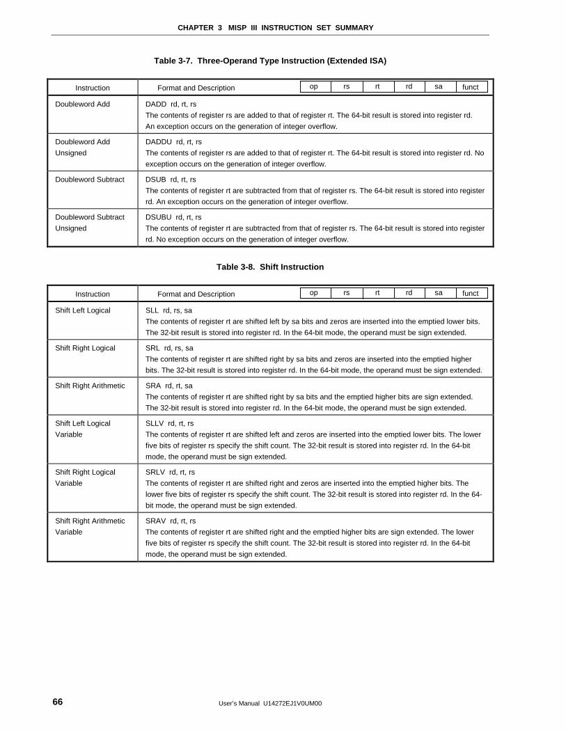
CHAPTER 3 MISP III INSTRUCTION SET SUMMARY
User’s Manual U14272EJ1V0UM0066
Table 3-7. Three-Operand Type Instruction (Extended ISA)
Instruction Format and Description
Doubleword Add DADD rd, rt, rs
The contents of register rs are added to that of register rt. The 64-bit result is stored into register rd.
An exception occurs on the generation of integer overflow.
Doubleword Add
Unsigned
DADDU rd, rt, rs
The contents of register rs are added to that of register rt. The 64-bit result is stored into register rd. No
exception occurs on the generation of integer overflow.
Doubleword Subtract DSUB rd, rt, rs
The contents of register rt are subtracted from that of register rs. The 64-bit result is stored into register
rd. An exception occurs on the generation of integer overflow.
Doubleword Subtract
Unsigned
DSUBU rd, rt, rs
The contents of register rt are subtracted from that of register rs. The 64-bit result is stored into register
rd. No exception occurs on the generation of integer overflow.
Table 3-8. Shift Instruction
Instruction Format and Description
Shift Left Logical SLL rd, rs, sa
The contents of register rt are shifted left by sa bits and zeros are inserted into the emptied lower bits.
The 32-bit result is stored into register rd. In the 64-bit mode, the operand must be sign extended.
Shift Right Logical SRL rd, rs, sa
The contents of register rt are shifted right by sa bits and zeros are inserted into the emptied higher
bits. The 32-bit result is stored into register rd. In the 64-bit mode, the operand must be sign extended.
Shift Right Arithmetic SRA rd, rt, sa
The contents of register rt are shifted right by sa bits and the emptied higher bits are sign extended.
The 32-bit result is stored into register rd. In the 64-bit mode, the operand must be sign extended.
Shift Left Logical
Variable
SLLV rd, rt, rs
The contents of register rt are shifted left and zeros are inserted into the emptied lower bits. The lower
five bits of register rs specify the shift count. The 32-bit result is stored into register rd. In the 64-bit
mode, the operand must be sign extended.
Shift Right Logical
Variable
SRLV rd, rt, rs
The contents of register rt are shifted right and zeros are inserted into the emptied higher bits. The
lower five bits of register rs specify the shift count. The 32-bit result is stored into register rd. In the 64-
bit mode, the operand must be sign extended.
Shift Right Arithmetic
Variable
SRAV rd, rt, rs
The contents of register rt are shifted right and the emptied higher bits are sign extended. The lower
five bits of register rs specify the shift count. The 32-bit result is stored into register rd. In the 64-bit
mode, the operand must be sign extended.
op rs rt functrd sa
op rs rt functrd sa
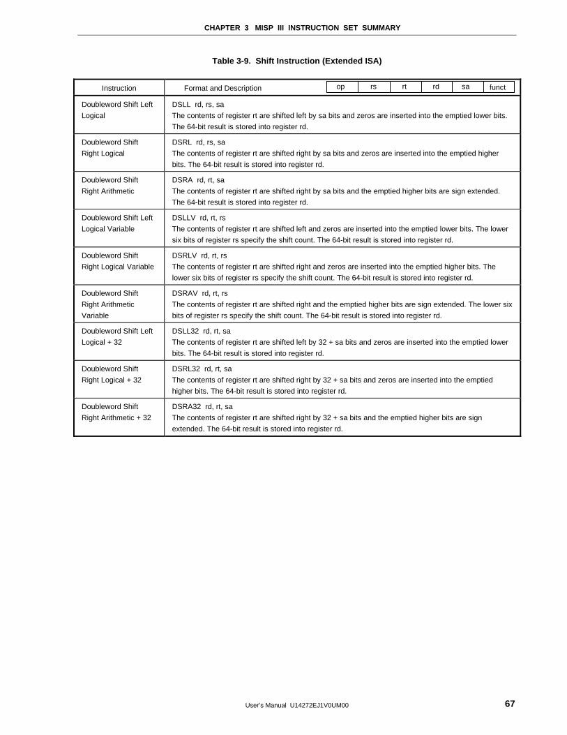
CHAPTER 3 MISP III INSTRUCTION SET SUMMARY
User’s Manual U14272EJ1V0UM00 67
Table 3-9. Shift Instruction (Extended ISA)
Instruction Format and Description
Doubleword Shift Left
Logical
DSLL rd, rs, sa
The contents of register rt are shifted left by sa bits and zeros are inserted into the emptied lower bits.
The 64-bit result is stored into register rd.
Doubleword Shift
Right Logical
DSRL rd, rs, sa
The contents of register rt are shifted right by sa bits and zeros are inserted into the emptied higher
bits. The 64-bit result is stored into register rd.
Doubleword Shift
Right Arithmetic
DSRA rd, rt, sa
The contents of register rt are shifted right by sa bits and the emptied higher bits are sign extended.
The 64-bit result is stored into register rd.
Doubleword Shift Left
Logical Variable
DSLLV rd, rt, rs
The contents of register rt are shifted left and zeros are inserted into the emptied lower bits. The lower
six bits of register rs specify the shift count. The 64-bit result is stored into register rd.
Doubleword Shift
Right Logical Variable
DSRLV rd, rt, rs
The contents of register rt are shifted right and zeros are inserted into the emptied higher bits. The
lower six bits of register rs specify the shift count. The 64-bit result is stored into register rd.
Doubleword Shift
Right Arithmetic
Variable
DSRAV rd, rt, rs
The contents of register rt are shifted right and the emptied higher bits are sign extended. The lower six
bits of register rs specify the shift count. The 64-bit result is stored into register rd.
Doubleword Shift Left
Logical + 32
DSLL32 rd, rt, sa
The contents of register rt are shifted left by 32 + sa bits and zeros are inserted into the emptied lower
bits. The 64-bit result is stored into register rd.
Doubleword Shift
Right Logical + 32
DSRL32 rd, rt, sa
The contents of register rt are shifted right by 32 + sa bits and zeros are inserted into the emptied
higher bits. The 64-bit result is stored into register rd.
Doubleword Shift
Right Arithmetic + 32
DSRA32 rd, rt, sa
The contents of register rt are shifted right by 32 + sa bits and the emptied higher bits are sign
extended. The 64-bit result is stored into register rd.
op rs rt functrd sa
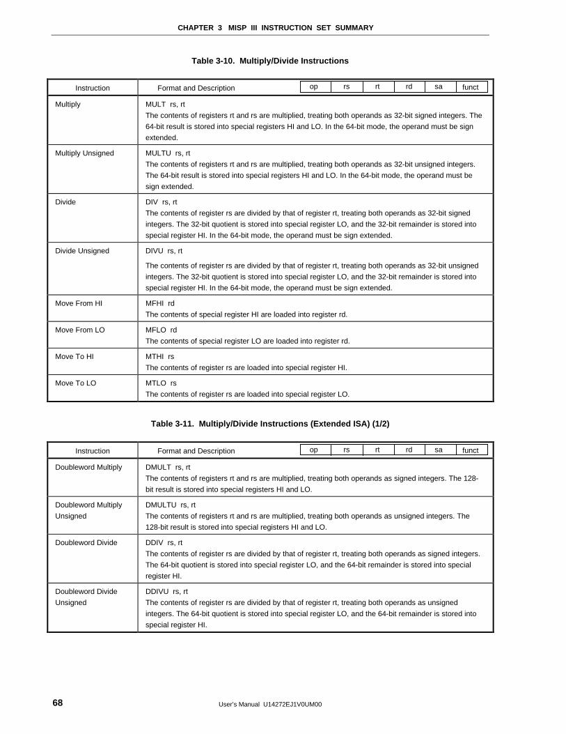
CHAPTER 3 MISP III INSTRUCTION SET SUMMARY
User’s Manual U14272EJ1V0UM0068
Table 3-10. Multiply/Divide Instructions
Instruction Format and Description
Multiply MULT rs, rt
The contents of registers rt and rs are multiplied, treating both operands as 32-bit signed integers. The
64-bit result is stored into special registers HI and LO. In the 64-bit mode, the operand must be sign
extended.
Multiply Unsigned MULTU rs, rt
The contents of registers rt and rs are multiplied, treating both operands as 32-bit unsigned integers.
The 64-bit result is stored into special registers HI and LO. In the 64-bit mode, the operand must be
sign extended.
Divide DIV rs, rt
The contents of register rs are divided by that of register rt, treating both operands as 32-bit signed
integers. The 32-bit quotient is stored into special register LO, and the 32-bit remainder is stored into
special register HI. In the 64-bit mode, the operand must be sign extended.
Divide Unsigned DIVU rs, rt
The contents of register rs are divided by that of register rt, treating both operands as 32-bit unsigned
integers. The 32-bit quotient is stored into special register LO, and the 32-bit remainder is stored into
special register HI. In the 64-bit mode, the operand must be sign extended.
Move From HI MFHI rd
The contents of special register HI are loaded into register rd.
Move From LO MFLO rd
The contents of special register LO are loaded into register rd.
Move To HI MTHI rs
The contents of register rs are loaded into special register HI.
Move To LO MTLO rs
The contents of register rs are loaded into special register LO.
Table 3-11. Multiply/Divide Instructions (Extended ISA) (1/2)
Instruction Format and Description
Doubleword Multiply DMULT rs, rt
The contents of registers rt and rs are multiplied, treating both operands as signed integers. The 128-
bit result is stored into special registers HI and LO.
Doubleword Multiply
Unsigned
DMULTU rs, rt
The contents of registers rt and rs are multiplied, treating both operands as unsigned integers. The
128-bit result is stored into special registers HI and LO.
Doubleword Divide DDIV rs, rt
The contents of register rs are divided by that of register rt, treating both operands as signed integers.
The 64-bit quotient is stored into special register LO, and the 64-bit remainder is stored into special
register HI.
Doubleword Divide
Unsigned
DDIVU rs, rt
The contents of register rs are divided by that of register rt, treating both operands as unsigned
integers. The 64-bit quotient is stored into special register LO, and the 64-bit remainder is stored into
special register HI.
op rs rt functrd sa
op rs rt functrd sa
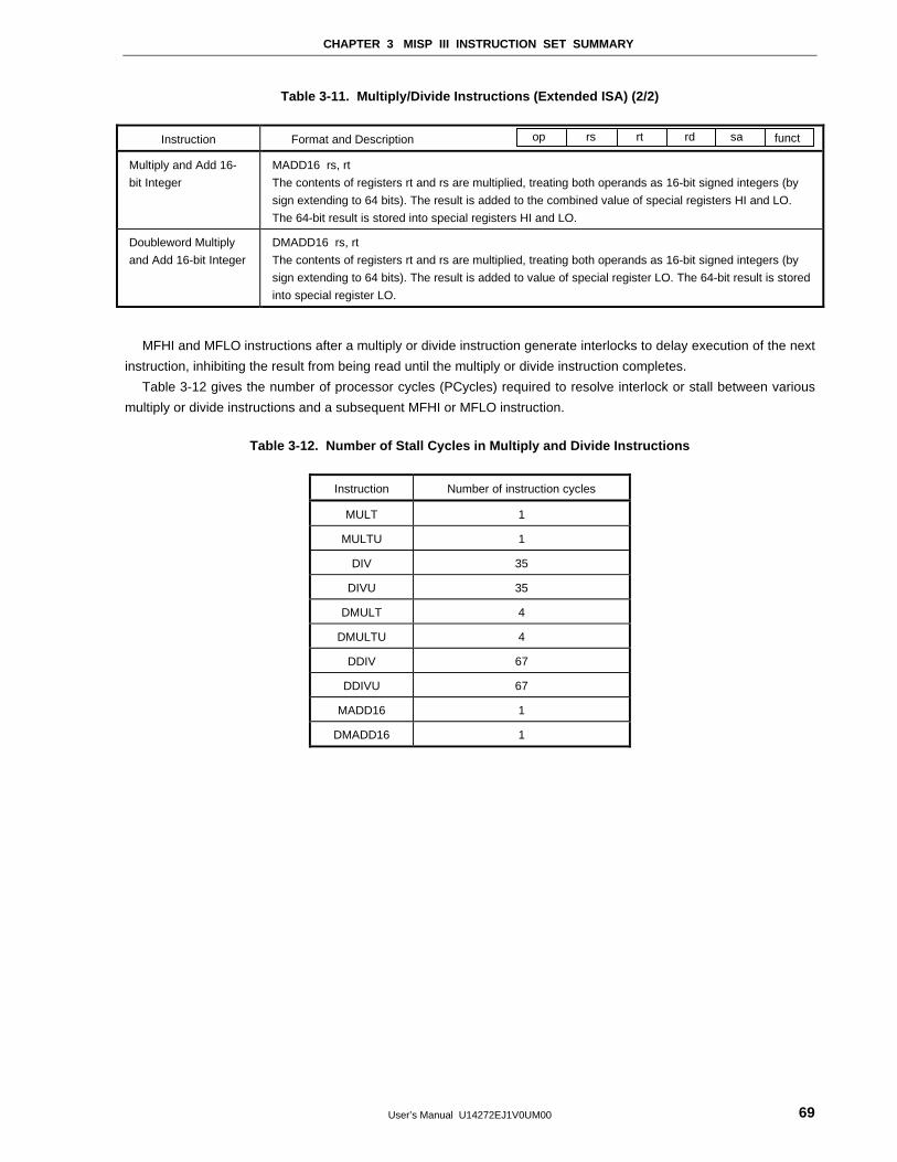
CHAPTER 3 MISP III INSTRUCTION SET SUMMARY
User’s Manual U14272EJ1V0UM00 69
Table 3-11. Multiply/Divide Instructions (Extended ISA) (2/2)
Instruction Format and Description
Multiply and Add 16-
bit Integer
MADD16 rs, rt
The contents of registers rt and rs are multiplied, treating both operands as 16-bit signed integers (by
sign extending to 64 bits). The result is added to the combined value of special registers HI and LO.
The 64-bit result is stored into special registers HI and LO.
Doubleword Multiply
and Add 16-bit Integer
DMADD16 rs, rt
The contents of registers rt and rs are multiplied, treating both operands as 16-bit signed integers (by
sign extending to 64 bits). The result is added to value of special register LO. The 64-bit result is stored
into special register LO.
MFHI and MFLO instructions after a multiply or divide instruction generate interlocks to delay execution of the next
instruction, inhibiting the result from being read until the multiply or divide instruction completes.
Table 3-12 gives the number of processor cycles (PCycles) required to resolve interlock or stall between various
multiply or divide instructions and a subsequent MFHI or MFLO instruction.
Table 3-12. Number of Stall Cycles in Multiply and Divide Instructions
Instruction Number of instruction cycles
MULT 1
MULTU 1
DIV 35
DIVU 35
DMULT 4
DMULTU 4
DDIV 67
DDIVU 67
MADD16 1
DMADD16 1
op rs rt functrd sa
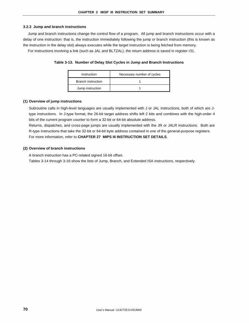
CHAPTER 3 MISP III INSTRUCTION SET SUMMARY
User’s Manual U14272EJ1V0UM0070
3.2.3 Jump and branch instructions
Jump and branch instructions change the control flow of a program. All jump and branch instructions occur with a
delay of one instruction: that is, the instruction immediately following the jump or branch instruction (this is known as
the instruction in the delay slot) always executes while the target instruction is being fetched from memory.
For instructions involving a link (such as JAL and BLTZAL), the return address is saved in register r31.
Table 3-13. Number of Delay Slot Cycles in Jump and Branch Instructions
Instruction Necessary number of cycles
Branch instruction 1
Jump instruction 1
(1) Overview of jump instructions
Subroutine calls in high-level languages are usually implemented with J or JAL instructions, both of which are J-
type instructions. In J-type format, the 26-bit target address shifts left 2 bits and combines with the high-order 4
bits of the current program counter to form a 32-bit or 64-bit absolute address.
Returns, dispatches, and cross-page jumps are usually implemented with the JR or JALR instructions. Both are
R-type instructions that take the 32-bit or 64-bit byte address contained in one of the general-purpose registers.
For more information, refer to CHAPTER 27 MIPS III INSTRUCTION SET DETAILS .
(2) Overview of branch instructions
A branch instruction has a PC-related signed 16-bit offset.
Tables 3-14 through 3-16 show the lists of Jump, Branch, and Extended ISA instructions, respectively.
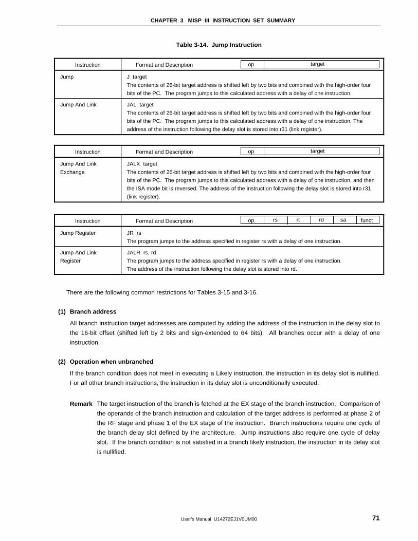
CHAPTER 3 MISP III INSTRUCTION SET SUMMARY
User’s Manual U14272EJ1V0UM00 71
Table 3-14. Jump Instruction
Instruction Format and Description
Jump J target
The contents of 26-bit target address is shifted left by two bits and combined with the high-order four
bits of the PC. The program jumps to this calculated address with a delay of one instruction.
Jump And Link JAL target
The contents of 26-bit target address is shifted left by two bits and combined with the high-order four
bits of the PC. The program jumps to this calculated address with a delay of one instruction. The
address of the instruction following the delay slot is stored into r31 (link register).
Instruction Format and Description
Jump And Link
Exchange
JALX target
The contents of 26-bit target address is shifted left by two bits and combined with the high-order four
bits of the PC. The program jumps to this calculated address with a delay of one instruction, and then
the ISA mode bit is reversed. The address of the instruction following the delay slot is stored into r31
(link register).
Instruction Format and Description
Jump Register JR rs
The program jumps to the address specified in register rs with a delay of one instruction.
Jump And Link
Register
JALR rs, rd
The program jumps to the address specified in register rs with a delay of one instruction.
The address of the instruction following the delay slot is stored into rd.
There are the following common restrictions for Tables 3-15 and 3-16.
(1) Branch address
All branch instruction target addresses are computed by adding the address of the instruction in the delay slot to
the 16-bit offset (shifted left by 2 bits and sign-extended to 64 bits). All branches occur with a delay of one
instruction.
(2) Operation when unbranched
If the branch condition does not meet in executing a Likely instruction, the instruction in its delay slot is nullified.
For all other branch instructions, the instruction in its delay slot is unconditionally executed.
Remark The target instruction of the branch is fetched at the EX stage of the branch instruction. Comparison of
the operands of the branch instruction and calculation of the target address is performed at phase 2 of
the RF stage and phase 1 of the EX stage of the instruction. Branch instructions require one cycle of
the branch delay slot defined by the architecture. Jump instructions also require one cycle of delay
slot. If the branch condition is not satisfied in a branch likely instruction, the instruction in its delay slot
is nullified.
op rs rt functrd sa
op target
op target
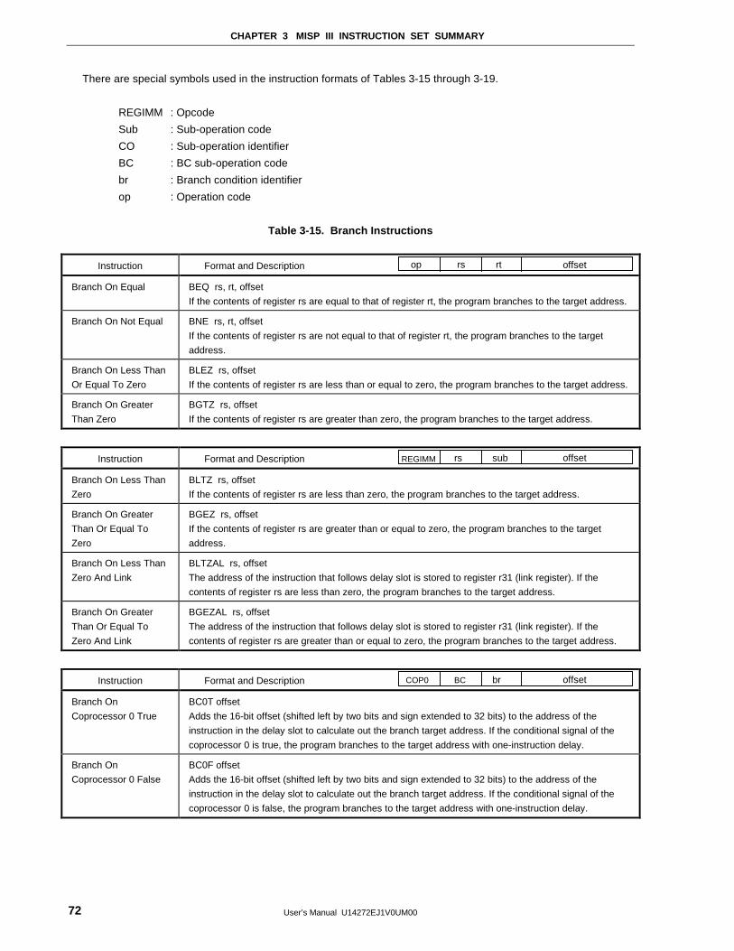
CHAPTER 3 MISP III INSTRUCTION SET SUMMARY
User’s Manual U14272EJ1V0UM0072
There are special symbols used in the instruction formats of Tables 3-15 through 3-19.
REGIMM : Opcode
Sub : Sub-operation code
CO : Sub-operation identifier
BC : BC sub-operation code
br : Branch condition identifier
op : Operation code
Table 3-15. Branch Instructions
Instruction Format and Description
Branch On Equal BEQ rs, rt, offset
If the contents of register rs are equal to that of register rt, the program branches to the target address.
Branch On Not Equal BNE rs, rt, offset
If the contents of register rs are not equal to that of register rt, the program branches to the target
address.
Branch On Less Than
Or Equal To Zero
BLEZ rs, offset
If the contents of register rs are less than or equal to zero, the program branches to the target address.
Branch On Greater
Than Zero
BGTZ rs, offset
If the contents of register rs are greater than zero, the program branches to the target address.
Instruction Format and Description
Branch On Less Than
Zero
BLTZ rs, offset
If the contents of register rs are less than zero, the program branches to the target address.
Branch On Greater
Than Or Equal To
Zero
BGEZ rs, offset
If the contents of register rs are greater than or equal to zero, the program branches to the target
address.
Branch On Less Than
Zero And Link
BLTZAL rs, offset
The address of the instruction that follows delay slot is stored to register r31 (link register). If the
contents of register rs are less than zero, the program branches to the target address.
Branch On Greater
Than Or Equal To
Zero And Link
BGEZAL rs, offset
The address of the instruction that follows delay slot is stored to register r31 (link register). If the
contents of register rs are greater than or equal to zero, the program branches to the target address.
Instruction Format and Description
Branch On
Coprocessor 0 True
BC0T offset
Adds the 16-bit offset (shifted left by two bits and sign extended to 32 bits) to the address of the
instruction in the delay slot to calculate out the branch target address. If the conditional signal of the
coprocessor 0 is true, the program branches to the target address with one-instruction delay.
Branch On
Coprocessor 0 False
BC0F offset
Adds the 16-bit offset (shifted left by two bits and sign extended to 32 bits) to the address of the
instruction in the delay slot to calculate out the branch target address. If the conditional signal of the
coprocessor 0 is false, the program branches to the target address with one-instruction delay.
op rs rt offset
REGIMM offsetrs sub
COP0 offsetBC br
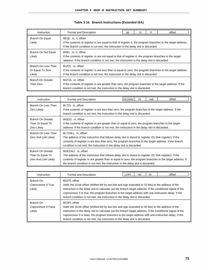
CHAPTER 3 MISP III INSTRUCTION SET SUMMARY
User’s Manual U14272EJ1V0UM00 73
Table 3-16. Branch Instructions (Extended ISA)
Instruction Format and Description
Branch On Equal
Likely
BEQL rs, rt, offset
If the contents of register rs are equal to that of register rt, the program branches to the target address.
If the branch condition is not met, the instruction in the delay slot is discarded.
Branch On Not Equal
Likely
BNEL rs, rt, offset
If the contents of register rs are not equal to that of register rt, the program branches to the target
address. If the branch condition is not met, the instruction in the delay slot is discarded.
Branch On Less Than
Or Equal To Zero
Likely
BLEZL rs, offset
If the contents of register rs are less than or equal to zero, the program branches to the target address.
If the branch condition is not met, the instruction in the delay slot is discarded.
Branch On Greater
Than Zero
BGTZL rs, offset
If the contents of register rs are greater than zero, the program branches to the target address. If the
branch condition is not met, the instruction in the delay slot is discarded.
Instruction Format and Description
Branch On Less Than
Zero Likely
BLTZL rs, offset
If the contents of register rs are less than zero, the program branches to the target address. If the
branch condition is not met, the instruction in the delay slot is discarded.
Branch On Greater
Than Or Equal To
Zero Likely
BGEZL rs, offset
If the contents of register rs are greater than or equal to zero, the program branches to the target
address. If the branch condition is not met, the instruction in the delay slot is discarded.
Branch On Less Than
Zero And Link Likely
BLTZALL rs, offset
The address of the instruction that follows delay slot is stored to register r31 (link register). If the
contents of register rs are less than zero, the program branches to the target address. If the branch
condition is not met, the instruction in the delay slot is discarded.
Branch On Greater
Than Or Equal To
Zero And Link Likely
BGEZALL rs, offset
The address of the instruction that follows delay slot is stored to register r31 (link register). If the
contents of register rs are greater than or equal to zero, the program branches to the target address. If
the branch condition is not met, the instruction in the delay slot is discarded.
Instruction Format and Description
Branch On
Coprocessor 0 True
Likely
BC0TL offset
Adds the 16-bit offset (shifted left by two bits and sign extended to 32 bits) to the address of the
instruction in the delay slot to calculate out the branch target address. If the conditional signal of the
coprocessor 0 is true, the program branches to the target address with one-instruction delay. If the
branch condition is not met, the instruction in the delay slot is discarded.
Branch On
Coprocessor 0 False
Likely
BC0FL offset
Adds the 16-bit offset (shifted left by two bits and sign extended to 32 bits) to the address of the
instruction in the delay slot to calculate out the branch target address. If the conditional signal of the
coprocessor 0 is false, the program branches to the target address with one-instruction delay. If the
branch condition is not met, the instruction in the delay slot is discarded.
op rs rt offset
REGIMM offsetrs sub
COP0 offsetBC br
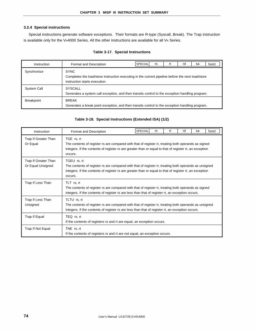
CHAPTER 3 MISP III INSTRUCTION SET SUMMARY
User’s Manual U14272EJ1V0UM0074
3.2.4 Special instructions
Special instructions generate software exceptions. Their formats are R-type (Syscall, Break). The Trap instruction
is available only for the VR4000 Series. All the other instructions are available for all VR Series.
Table 3-17. Special Instructions
Instruction Format and Description
Synchronize SYNC
Completes the load/store instruction executing in the current pipeline before the next load/store
instruction starts execution.
System Call SYSCALL
Generates a system call exception, and then transits control to the exception handling program.
Breakpoint BREAK
Generates a break point exception, and then transits control to the exception handling program.
Table 3-18. Special Instructions (Extended ISA) (1/2)
Instruction Format and Description
Trap If Greater Than
Or Equal
TGE rs, rt
The contents of register rs are compared with that of register rt, treating both operands as signed
integers. If the contents of register rs are greater than or equal to that of register rt, an exception
occurs.
Trap If Greater Than
Or Equal Unsigned
TGEU rs, rt
The contents of register rs are compared with that of register rt, treating both operands as unsigned
integers. If the contents of register rs are greater than or equal to that of register rt, an exception
occurs.
Trap If Less Than TLT rs, rt
The contents of register rs are compared with that of register rt, treating both operands as signed
integers. If the contents of register rs are less than that of register rt, an exception occurs.
Trap If Less Than
Unsigned
TLTU rs, rt
The contents of register rs are compared with that of register rt, treating both operands as unsigned
integers. If the contents of register rs are less than that of register rt, an exception occurs.
Trap If Equal TEQ rs, rt
If the contents of registers rs and rt are equal, an exception occurs.
Trap If Not Equal TNE rs, rt
If the contents of registers rs and rt are not equal, an exception occurs.
SPECIAL rs rt functrd sa
SPECIAL rs rt functrd sa
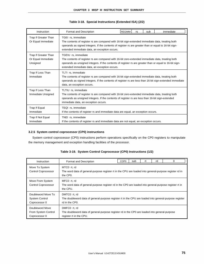
CHAPTER 3 MISP III INSTRUCTION SET SUMMARY
User’s Manual U14272EJ1V0UM00 75
Table 3-18. Special Instructions (Extended ISA) (2/2)
Instruction Format and Description
Trap If Greater Than
Or Equal Immediate
TGEI rs, immediate
The contents of register rs are compared with 16-bit sign-extended immediate data, treating both
operands as signed integers. If the contents of register rs are greater than or equal to 16-bit sign-
extended immediate data, an exception occurs.
Trap If Greater Than
Or Equal Immediate
Unsigned
TGEIU rs, immediate
The contents of register rs are compared with 16-bit zero-extended immediate data, treating both
operands as unsigned integers. If the contents of register rs are greater than or equal to 16-bit sign-
extended immediate data, an exception occurs.
Trap If Less Than
Immediate
TLTI rs, immediate
The contents of register rs are compared with 16-bit sign-extended immediate data, treating both
operands as signed integers. If the contents of register rs are less than 16-bit sign-extended immediate
data, an exception occurs.
Trap If Less Than
Immediate Unsigned
TLTIU rs, immediate
The contents of register rs are compared with 16-bit zero-extended immediate data, treating both
operands as unsigned integers. If the contents of register rs are less than 16-bit sign-extended
immediate data, an exception occurs.
Trap If Equal
Immediate
TEQI rs, immediate
If the contents of register rs and immediate data are equal, an exception occurs.
Trap If Not Equal
Immediate
TNEI rs, immediate
If the contents of register rs and immediate data are not equal, an exception occurs.
3.2.5 System control coprocessor (CP0) instructions
System control coprocessor (CP0) instructions perform operations specifically on the CP0 registers to manipulate
the memory management and exception handling facilities of the processor.
Table 3-19. System Control Coprocessor (CP0) Instructions (1/2)
Instruction Format and Description
Move To System
Control Coprocessor
MTC0 rt, rd
The word data of general-purpose register rt in the CPU are loaded into general-purpose register rd in
the CP0.
Move From System
Control Coprocessor
MFC0 rt, rd
The word data of general-purpose register rd in the CP0 are loaded into general-purpose register rt in
the CPU.
Doubleword Move To
System Control
Coprocessor 0
DMTC0 rt, rd
The doubleword data of general-purpose register rt in the CPU are loaded into general-purpose register
rd in the CP0.
Doubleword Move
From System Control
Coprocessor 0
DMFC0 rt, rd
The doubleword data of general-purpose register rd in the CP0 are loaded into general-purpose
register rt in the CPU.
REGIMM immediaters sub
COP0 sub rt 0rd
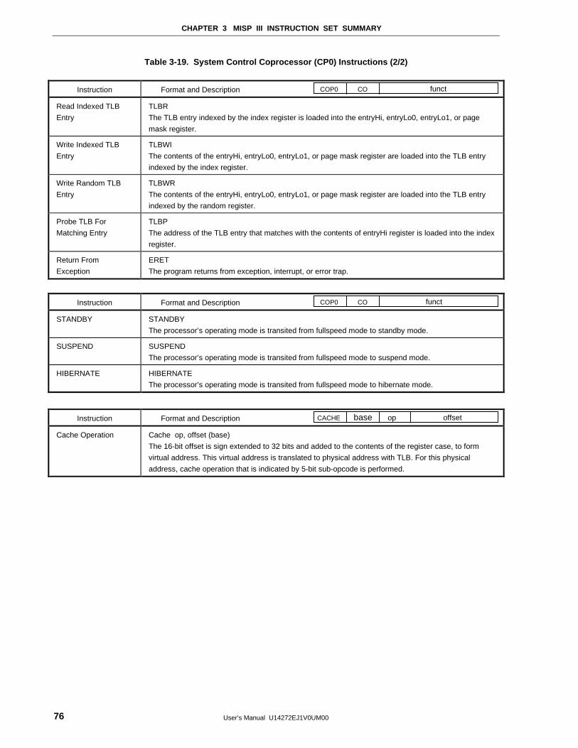
CHAPTER 3 MISP III INSTRUCTION SET SUMMARY
User’s Manual U14272EJ1V0UM0076
Table 3-19. System Control Coprocessor (CP0) Instructions (2/2)
Instruction Format and Description
Read Indexed TLB
Entry
TLBR
The TLB entry indexed by the index register is loaded into the entryHi, entryLo0, entryLo1, or page
mask register.
Write Indexed TLB
Entry
TLBWI
The contents of the entryHi, entryLo0, entryLo1, or page mask register are loaded into the TLB entry
indexed by the index register.
Write Random TLB
Entry
TLBWR
The contents of the entryHi, entryLo0, entryLo1, or page mask register are loaded into the TLB entry
indexed by the random register.
Probe TLB For
Matching Entry
TLBP
The address of the TLB entry that matches with the contents of entryHi register is loaded into the index
register.
Return From
Exception
ERET
The program returns from exception, interrupt, or error trap.
Instruction Format and Description
STANDBY STANDBY
The processor’s operating mode is transited from fullspeed mode to standby mode.
SUSPEND SUSPEND
The processor’s operating mode is transited from fullspeed mode to suspend mode.
HIBERNATE HIBERNATE
The processor’s operating mode is transited from fullspeed mode to hibernate mode.
Instruction Format and Description
Cache Operation Cache op, offset (base)
The 16-bit offset is sign extended to 32 bits and added to the contents of the register case, to form
virtual address. This virtual address is translated to physical address with TLB. For this physical
address, cache operation that is indicated by 5-bit sub-opcode is performed.
COP0 functCO
CACHE offsetbase op
COP0 functCO
User’s Manual U14272EJ1V0UM00 77
CHAPTER 4 MIPS16 INSTRUCTION SET
4.1 Outline
If the MIPS16 ASE (Application-Specific Extension), which is an expanded function for MIPS ISA (Instruction Set
Architecture), is used, system costs can be considerably reduced by lowering the memory capacity requirement of
embedded hardware. MIPS16 is an instruction set that uses the 16-bit instruction length, and is compatible with MIPS
I, II, III, IV, and VNote instruction sets in any combination. Moreover, 32-bit instruction length binary data can be
executed with the VR4181.
Note The VR4100 SeriesTM currently supports the MIPS I, II, and III instruction sets.
4.2 Features
• 16-bit length instruction format
• Reduces memory capacity requirements to lower overall system cost
• MIPS16 instructions can be used with MIPS instruction binary
• Compatibility with MIPS I, II, III, IV, and V instruction sets
• Used with switching between MIPS16 instruction length mode and 32-bit MIPS instruction length mode.
• Supports 8-bit, 16-bit, 32-bit, and 64-bit data formats
• Provides 8 general-purpose registers and special registers
• Improved code generation efficiency using special 16-bit dedicated instructions
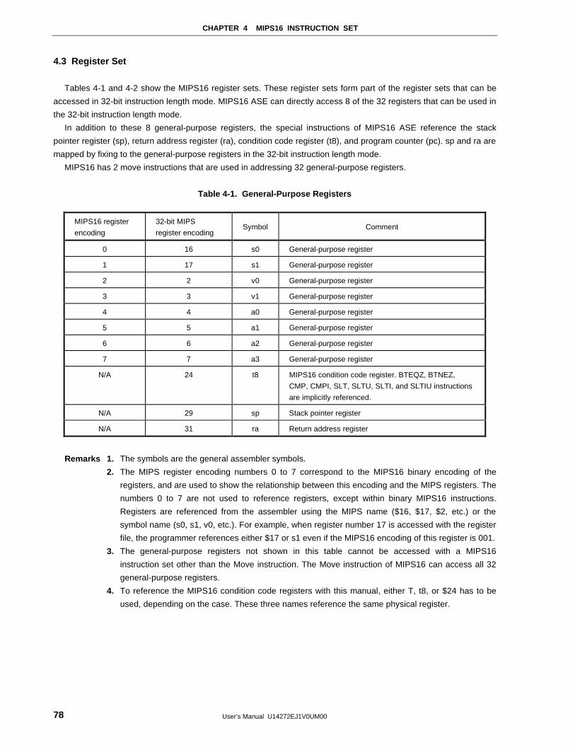
CHAPTER 4 MIPS16 INSTRUCTION SET
User’s Manual U14272EJ1V0UM0078
4.3 Register Set
Tables 4-1 and 4-2 show the MIPS16 register sets. These register sets form part of the register sets that can be
accessed in 32-bit instruction length mode. MIPS16 ASE can directly access 8 of the 32 registers that can be used in
the 32-bit instruction length mode.
In addition to these 8 general-purpose registers, the special instructions of MIPS16 ASE reference the stack
pointer register (sp), return address register (ra), condition code register (t8), and program counter (pc). sp and ra are
mapped by fixing to the general-purpose registers in the 32-bit instruction length mode.
MIPS16 has 2 move instructions that are used in addressing 32 general-purpose registers.
Table 4-1. General-Purpose Registers
MIPS16 register
encoding
32-bit MIPS
register encodingSymbol Comment
0 16 s0 General-purpose register
1 17 s1 General-purpose register
2 2 v0 General-purpose register
3 3 v1 General-purpose register
4 4 a0 General-purpose register
5 5 a1 General-purpose register
6 6 a2 General-purpose register
7 7 a3 General-purpose register
N/A 24 t8 MIPS16 condition code register. BTEQZ, BTNEZ,
CMP, CMPI, SLT, SLTU, SLTI, and SLTIU instructions
are implicitly referenced.
N/A 29 sp Stack pointer register
N/A 31 ra Return address register
Remarks 1. The symbols are the general assembler symbols.
2. The MIPS register encoding numbers 0 to 7 correspond to the MIPS16 binary encoding of the
registers, and are used to show the relationship between this encoding and the MIPS registers. The
numbers 0 to 7 are not used to reference registers, except within binary MIPS16 instructions.
Registers are referenced from the assembler using the MIPS name ($16, $17, $2, etc.) or the
symbol name (s0, s1, v0, etc.). For example, when register number 17 is accessed with the register
file, the programmer references either $17 or s1 even if the MIPS16 encoding of this register is 001.
3. The general-purpose registers not shown in this table cannot be accessed with a MIPS16
instruction set other than the Move instruction. The Move instruction of MIPS16 can access all 32
general-purpose registers.
4. To reference the MIPS16 condition code registers with this manual, either T, t8, or $24 has to be
used, depending on the case. These three names reference the same physical register.
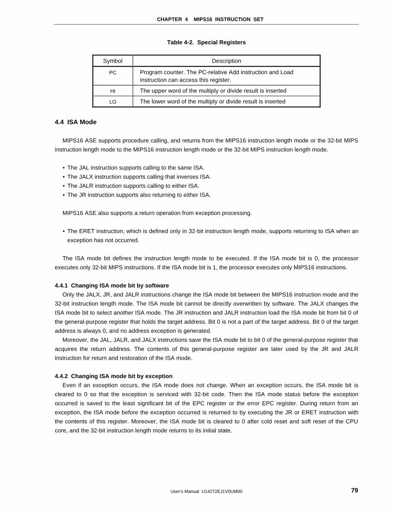
CHAPTER 4 MIPS16 INSTRUCTION SET
User’s Manual U14272EJ1V0UM00 79
Table 4-2. Special Registers
Symbol Description
PC Program counter. The PC-relative Add instruction and Loadinstruction can access this register.
HI The upper word of the multiply or divide result is inserted
LO The lower word of the multiply or divide result is inserted
4.4 ISA Mode
MIPS16 ASE supports procedure calling, and returns from the MIPS16 instruction length mode or the 32-bit MIPS
instruction length mode to the MIPS16 instruction length mode or the 32-bit MIPS instruction length mode.
• The JAL instruction supports calling to the same ISA.
• The JALX instruction supports calling that inverses ISA.
• The JALR instruction supports calling to either ISA.
• The JR instruction supports also returning to either ISA.
MIPS16 ASE also supports a return operation from exception processing.
• The ERET instruction, which is defined only in 32-bit instruction length mode, supports returning to ISA when an
exception has not occurred.
The ISA mode bit defines the instruction length mode to be executed. If the ISA mode bit is 0, the processor
executes only 32-bit MIPS instructions. If the ISA mode bit is 1, the processor executes only MIPS16 instructions.
4.4.1 Changing ISA mode bit by software
Only the JALX, JR, and JALR instructions change the ISA mode bit between the MIPS16 instruction mode and the
32-bit instruction length mode. The ISA mode bit cannot be directly overwritten by software. The JALX changes the
ISA mode bit to select another ISA mode. The JR instruction and JALR instruction load the ISA mode bit from bit 0 of
the general-purpose register that holds the target address. Bit 0 is not a part of the target address. Bit 0 of the target
address is always 0, and no address exception is generated.
Moreover, the JAL, JALR, and JALX instructions save the ISA mode bit to bit 0 of the general-purpose register that
acquires the return address. The contents of this general-purpose register are later used by the JR and JALR
instruction for return and restoration of the ISA mode.
4.4.2 Changing ISA mode bit by exception
Even if an exception occurs, the ISA mode does not change. When an exception occurs, the ISA mode bit is
cleared to 0 so that the exception is serviced with 32-bit code. Then the ISA mode status before the exception
occurred is saved to the least significant bit of the EPC register or the error EPC register. During return from an
exception, the ISA mode before the exception occurred is returned to by executing the JR or ERET instruction with
the contents of this register. Moreover, the ISA mode bit is cleared to 0 after cold reset and soft reset of the CPU
core, and the 32-bit instruction length mode returns to its initial state.
CHAPTER 4 MIPS16 INSTRUCTION SET
User’s Manual U14272EJ1V0UM0080
4.4.3 Enabling change ISA mode bit
Changing the ISA mode bit is valid only MIPS16EN is set to active when the RTCRST is selected, and the MIPS16
instruction mode is enabled. The operation of the JALX, JALR, JR, and ERET instructions in the 32-bit instruction
mode, differs depending on whether the MIPS16 instruction mode is enabled or prohibited. If the MIPS16 instruction
mode is prohibited, the JALX instruction generates a reserved instruction exception. The JR and JALR instructions
generate an address exception when bit 0 of the source register is 1. The ERET instruction generates an address
exception when bit 0 of the EPC or error EPC register is 1. If the MIPS16 instruction mode is enabled, the JALX
instruction executes JAL, and the ISA mode bit is inverted. The JR and JALR instructions load the ISA mode from bit
0 of the source register. The ERET instruction loads the ISA mode from bit 0 of the EPC or error EPC register. Bit 0
of the target address is always 0, and no address exception is generated even when bit 0 of the source register is 1.
4.5 Types of Instructions
This section describes the different types of instructions, and indicates the MIPS16 instructions included in each
group.
Instructions are divided into the following types.
Load and Store instructions : Move data between memory and the general-purpose registers.
Computational instructions : Perform arithmetic operations, logical operations, and shift operations on values
in registers.
Jump and Branch instructions: Change the control flow of a program.
Special instructions : Break instructions and Extend instructions. Break transfers control to an
exception handler. Extend enlarges the immediate field of the next instruction.
Instructions that can be extended with Extend are indicated as Note 1 in Table
4-3 MIPS16 Instruction Set Outline .
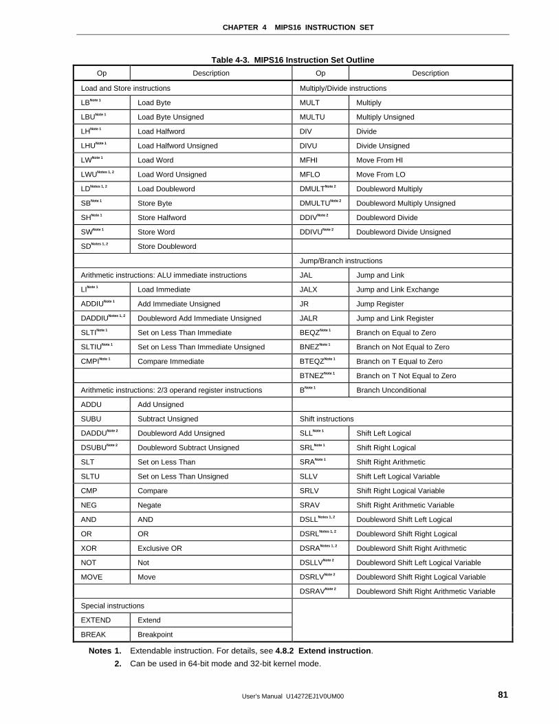
CHAPTER 4 MIPS16 INSTRUCTION SET
User’s Manual U14272EJ1V0UM00 81
Table 4-3. MIPS16 Instruction Set Outline
Op Description Op Description
Load and Store instructions Multiply/Divide instructions
LBNote 1 Load Byte MULT Multiply
LBUNote 1 Load Byte Unsigned MULTU Multiply Unsigned
LHNote 1 Load Halfword DIV Divide
LHUNote 1 Load Halfword Unsigned DIVU Divide Unsigned
LWNote 1 Load Word MFHI Move From HI
LWUNotes 1, 2 Load Word Unsigned MFLO Move From LO
LDNotes 1, 2 Load Doubleword DMULTNote 2 Doubleword Multiply
SBNote 1 Store Byte DMULTUNote 2 Doubleword Multiply Unsigned
SHNote 1 Store Halfword DDIVNote 2 Doubleword Divide
SWNote 1 Store Word DDIVUNote 2 Doubleword Divide Unsigned
SDNotes 1, 2 Store Doubleword
Jump/Branch instructions
Arithmetic instructions: ALU immediate instructions JAL Jump and Link
LINote 1 Load Immediate JALX Jump and Link Exchange
ADDIUNote 1 Add Immediate Unsigned JR Jump Register
DADDIUNotes 1, 2 Doubleword Add Immediate Unsigned JALR Jump and Link Register
SLTINote 1 Set on Less Than Immediate BEQZNote 1 Branch on Equal to Zero
SLTIUNote 1 Set on Less Than Immediate Unsigned BNEZNote 1 Branch on Not Equal to Zero
CMPINote 1 Compare Immediate BTEQZNote 1 Branch on T Equal to Zero
BTNEZNote 1 Branch on T Not Equal to Zero
Arithmetic instructions: 2/3 operand register instructions BNote 1 Branch Unconditional
ADDU Add Unsigned
SUBU Subtract Unsigned Shift instructions
DADDUNote 2 Doubleword Add Unsigned SLLNote 1 Shift Left Logical
DSUBUNote 2 Doubleword Subtract Unsigned SRLNote 1 Shift Right Logical
SLT Set on Less Than SRANote 1 Shift Right Arithmetic
SLTU Set on Less Than Unsigned SLLV Shift Left Logical Variable
CMP Compare SRLV Shift Right Logical Variable
NEG Negate SRAV Shift Right Arithmetic Variable
AND AND DSLLNotes 1, 2 Doubleword Shift Left Logical
OR OR DSRLNotes 1, 2 Doubleword Shift Right Logical
XOR Exclusive OR DSRANotes 1, 2 Doubleword Shift Right Arithmetic
NOT Not DSLLVNote 2 Doubleword Shift Left Logical Variable
MOVE Move DSRLVNote 2 Doubleword Shift Right Logical Variable
DSRAVNote 2 Doubleword Shift Right Arithmetic Variable
Special instructions
EXTEND Extend
BREAK Breakpoint
Notes 1. Extendable instruction. For details, see 4.8.2 Extend instruction .
2. Can be used in 64-bit mode and 32-bit kernel mode.
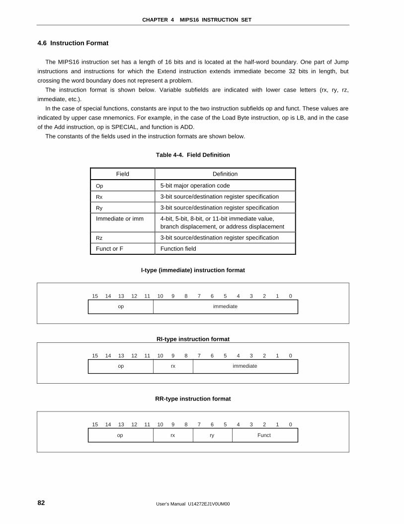
CHAPTER 4 MIPS16 INSTRUCTION SET
User’s Manual U14272EJ1V0UM0082
4.6 Instruction Format
The MIPS16 instruction set has a length of 16 bits and is located at the half-word boundary. One part of Jump
instructions and instructions for which the Extend instruction extends immediate become 32 bits in length, but
crossing the word boundary does not represent a problem.
The instruction format is shown below. Variable subfields are indicated with lower case letters (rx, ry, rz,
immediate, etc.).
In the case of special functions, constants are input to the two instruction subfields op and funct. These values are
indicated by upper case mnemonics. For example, in the case of the Load Byte instruction, op is LB, and in the case
of the Add instruction, op is SPECIAL, and function is ADD.
The constants of the fields used in the instruction formats are shown below.
Table 4-4. Field Definition
Field Definition
Op 5-bit major operation code
Rx 3-bit source/destination register specification
Ry 3-bit source/destination register specification
Immediate or imm 4-bit, 5-bit, 8-bit, or 11-bit immediate value,branch displacement, or address displacement
Rz 3-bit source/destination register specification
Funct or F Function field
I-type (immediate) instruction format
15 14 13 12 11 10 9 8 7 6 5 4 3 2 1 0
op immediate
RI-type instruction format
15 14 13 12 11 10 9 8 7 6 5 4 3 2 1 0
op rx immediate
RR-type instruction format
15 14 13 12 11 10 9 8 7 6 5 4 3 2 1 0
op rx ry Funct
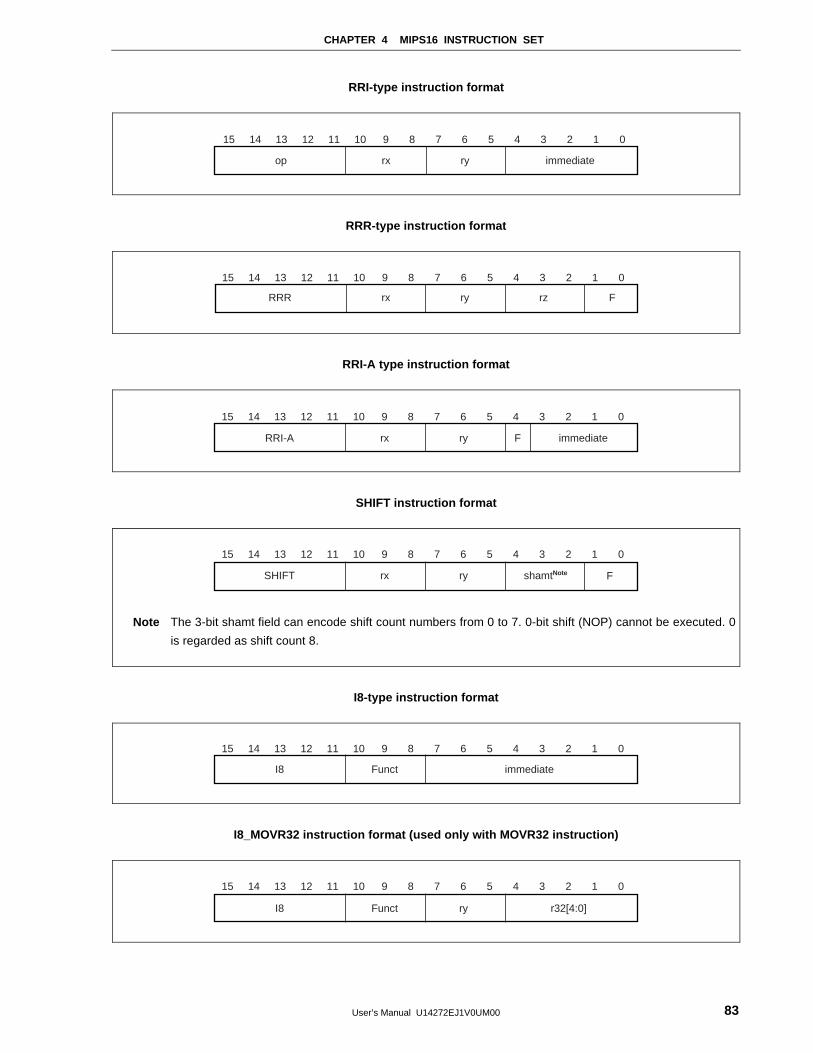
CHAPTER 4 MIPS16 INSTRUCTION SET
User’s Manual U14272EJ1V0UM00 83
RRI-type instruction format
15 14 13 12 11 10 9 8 7 6 5 4 3 2 1 0
op rx ry immediate
RRR-type instruction format
15 14 13 12 11 10 9 8 7 6 5 4 3 2 1 0
RRR rx ry rz F
RRI-A type instruction format
15 14 13 12 11 10 9 8 7 6 5 4 3 2 1 0
RRI-A rx ry F immediate
SHIFT instruction format
15 14 13 12 11 10 9 8 7 6 5 4 3 2 1 0
SHIFT rx ry shamtNote F
Note The 3-bit shamt field can encode shift count numbers from 0 to 7. 0-bit shift (NOP) cannot be executed. 0
is regarded as shift count 8.
I8-type instruction format
15 14 13 12 11 10 9 8 7 6 5 4 3 2 1 0
I8 Funct immediate
I8_MOVR32 instruction format (used only with MOVR32 instruction)
15 14 13 12 11 10 9 8 7 6 5 4 3 2 1 0
I8 Funct ry r32[4:0]
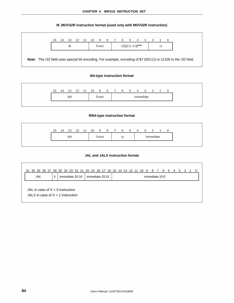
CHAPTER 4 MIPS16 INSTRUCTION SET
User’s Manual U14272EJ1V0UM0084
I8_MOV32R instruction format (used only with MOV32R instruction)
15 14 13 12 11 10 9 8 7 6 5 4 3 2 1 0
I8 Funct r32[2:0, 4:3]Note rz
Note The r32 field uses special bit encoding. For example, encoding of $7 (00111) is 11100 in the r32 field.
I64-type instruction format
15 14 13 12 11 10 9 8 7 6 5 4 3 2 1 0
I64 Funct immediate
RI64-type instruction format
15 14 13 12 11 10 9 8 7 6 5 4 3 2 1 0
I64 Funct ry immediate
JAL and JALX instruction format
31 30 29 28 27 26 25 24 23 22 21 20 19 18 17 16 15 14 13 12 11 10 9 8 7 6 5 4 3 2 1 0
JAL X immediate 20:16 immediate 25:21 immediate 15:0
JAL in case of X = 0 instruction
JALX in case of X = 1 instruction
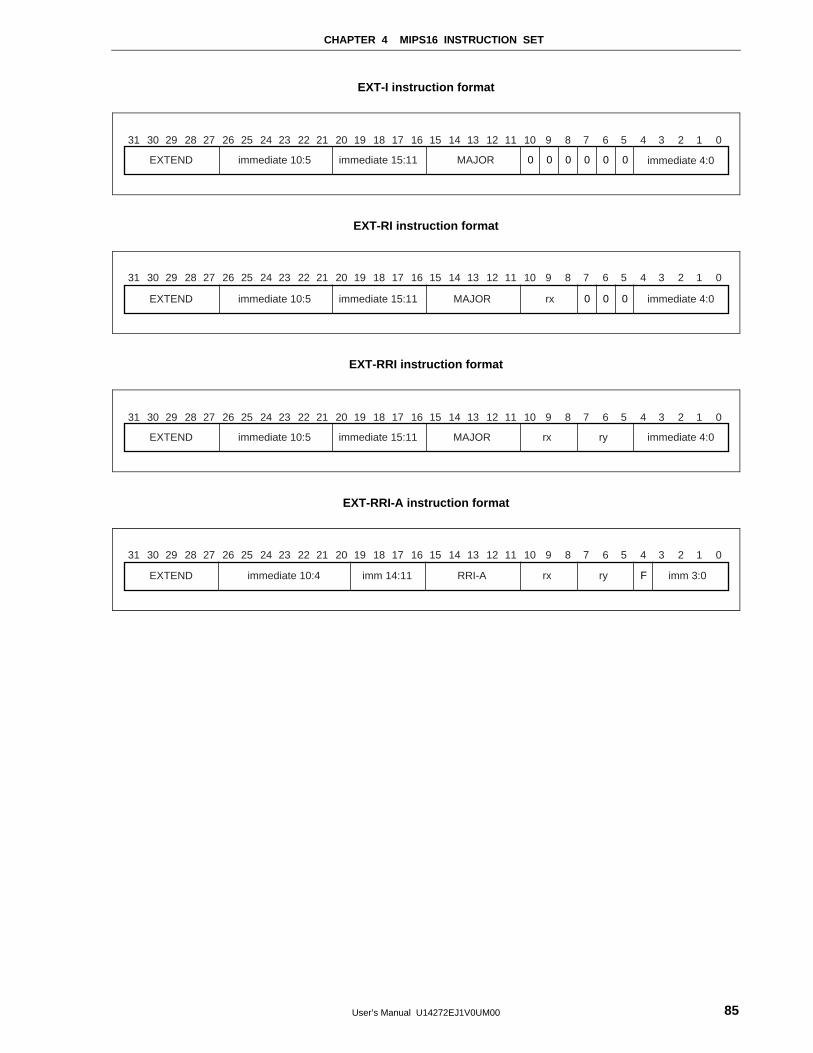
CHAPTER 4 MIPS16 INSTRUCTION SET
User’s Manual U14272EJ1V0UM00 85
EXT-I instruction format
31 30 29 28 27 26 25 24 23 22 21 20 19 18 17 16 15 14 13 12 11 10 9 8 7 6 5 4 3 2 1 0
EXTEND immediate 10:5 immediate 15:11 MAJOR 0 0 0 0 0 0 immediate 4:0
EXT-RI instruction format
31 30 29 28 27 26 25 24 23 22 21 20 19 18 17 16 15 14 13 12 11 10 9 8 7 6 5 4 3 2 1 0
EXTEND immediate 10:5 immediate 15:11 MAJOR rx 0 0 0 immediate 4:0
EXT-RRI instruction format
31 30 29 28 27 26 25 24 23 22 21 20 19 18 17 16 15 14 13 12 11 10 9 8 7 6 5 4 3 2 1 0
EXTEND immediate 10:5 immediate 15:11 MAJOR rx ry immediate 4:0
EXT-RRI-A instruction format
31 30 29 28 27 26 25 24 23 22 21 20 19 18 17 16 15 14 13 12 11 10 9 8 7 6 5 4 3 2 1 0
EXTEND immediate 10:4 imm 14:11 RRI-A rx ry imm 3:0F
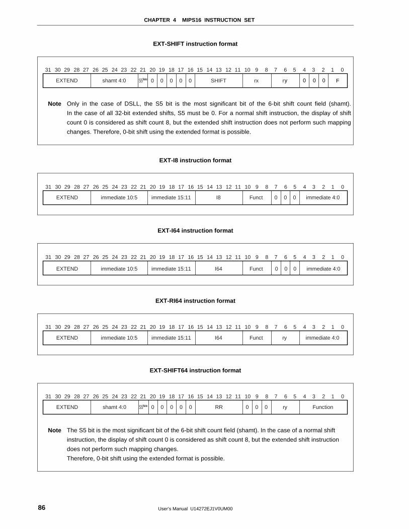
CHAPTER 4 MIPS16 INSTRUCTION SET
User’s Manual U14272EJ1V0UM0086
EXT-SHIFT instruction format
31 30 29 28 27 26 25 24 23 22 21 20 19 18 17 16 15 14 13 12 11 10 9 8 7 6 5 4 3 2 1 0
EXTEND shamt 4:0 S5Note 0 0 0 0 0 SHIFT rx r 0 0 F0y
Note Only in the case of DSLL, the S5 bit is the most significant bit of the 6-bit shift count field (shamt).
In the case of all 32-bit extended shifts, S5 must be 0. For a normal shift instruction, the display of shift
count 0 is considered as shift count 8, but the extended shift instruction does not perform such mapping
changes. Therefore, 0-bit shift using the extended format is possible.
EXT-I8 instruction format
31 30 29 28 27 26 25 24 23 22 21 20 19 18 17 16 15 14 13 12 11 10 9 8 7 6 5 4 3 2 1 0
EXTEND immediate 10:5 immediate 15:11 I8 Funct 0 0 0 immediate 4:0
EXT-I64 instruction format
31 30 29 28 27 26 25 24 23 22 21 20 19 18 17 16 15 14 13 12 11 10 9 8 7 6 5 4 3 2 1 0
EXTEND immediate 10:5 immediate 15:11 I64 Funct 0 0 0 immediate 4:0
EXT-RI64 instruction format
31 30 29 28 27 26 25 24 23 22 21 20 19 18 17 16 15 14 13 12 11 10 9 8 7 6 5 4 3 2 1 0
EXTEND immediate 10:5 immediate 15:11 I64 Funct ry immediate 4:0
EXT-SHIFT64 instruction format
31 30 29 28 27 26 25 24 23 22 21 20 19 18 17 16 15 14 13 12 11 10 9 8 7 6 5 4 3 2 1 0
EXTEND shamt 4:0 S5Note 0 0 0 0 0 RR 0 0 0 ry Function
Note The S5 bit is the most significant bit of the 6-bit shift count field (shamt). In the case of a normal shift
instruction, the display of shift count 0 is considered as shift count 8, but the extended shift instruction
does not perform such mapping changes.
Therefore, 0-bit shift using the extended format is possible.
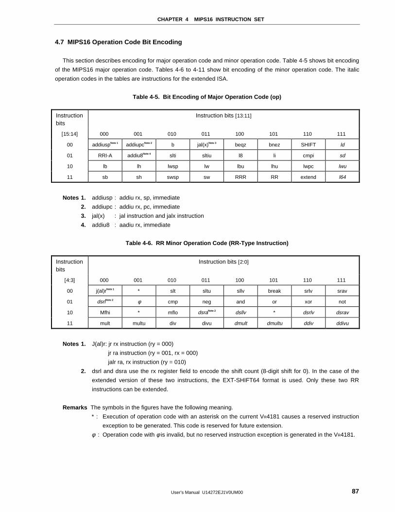
CHAPTER 4 MIPS16 INSTRUCTION SET
User’s Manual U14272EJ1V0UM00 87
4.7 MIPS16 Operation Code Bit Encoding
This section describes encoding for major operation code and minor operation code. Table 4-5 shows bit encoding
of the MIPS16 major operation code. Tables 4-6 to 4-11 show bit encoding of the minor operation code. The italic
operation codes in the tables are instructions for the extended ISA.
Table 4-5. Bit Encoding of Major Operation Code (op)
Instructionbits
Instruction bits [13:11]
[15:14] 000 001 010 011 100 101 110 111
00 addiuspNote 1 addiupcNote 2 b jal(x)Note 3 beqz bnez SHIFT ld
01 RRI-A addiu8Note 4 slti sltiu l8 li cmpi sd
10 lb lh lwsp lw lbu lhu lwpc lwu
11 sb sh swsp sw RRR RR extend l64
Notes 1. addiusp : addiu rx, sp, immediate
2. addiupc : addiu rx, pc, immediate
3. jal(x) : jal instruction and jalx instruction
4. addiu8 : aadiu rx, immediate
Table 4-6. RR Minor Operation Code (RR-Type Instruction)
Instructionbits
Instruction bits [2:0]
[4:3] 000 001 010 011 100 101 110 111
00 j(al)rNote 1 ∗ slt sltu sllv break srlv srav
01 dsrlNote 2 φ cmp neg and or xor not
10 Mfhi ∗ mflo dsraNote 2 dsllv ∗ dsrlv dsrav
11 mult multu div divu dmult dmultu ddiv ddivu
Notes 1. J(al)r: jr rx instruction (ry = 000)
jr ra instruction (ry = 001, rx = 000)
jalr ra, rx instruction (ry = 010)
2. dsrl and dsra use the rx register field to encode the shift count (8-digit shift for 0). In the case of the
extended version of these two instructions, the EXT-SHIFT64 format is used. Only these two RR
instructions can be extended.
Remarks The symbols in the figures have the following meaning.
∗ : Execution of operation code with an asterisk on the current VR4181 causes a reserved instruction
exception to be generated. This code is reserved for future extension.
φ : Operation code with φ is invalid, but no reserved instruction exception is generated in the VR4181.
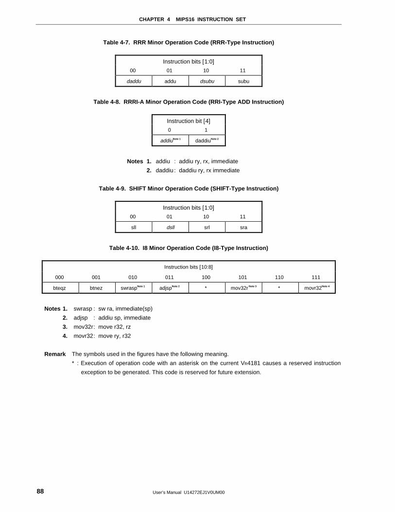
CHAPTER 4 MIPS16 INSTRUCTION SET
User’s Manual U14272EJ1V0UM0088
Table 4-7. RRR Minor Operation Code (RRR-Type Instruction)
Instruction bits [1:0]00 01 10 11
daddu addu dsubu subu
Table 4-8. RRRI-A Minor Operation Code (RRI-Type ADD Instruction)
Instruction bit [4]0 1
addiuNote 1 daddiuNote 2
Notes 1. addiu : addiu ry, rx, immediate
2. daddiu : daddiu ry, rx immediate
Table 4-9. SHIFT Minor Operation Code (SHIFT-Type Instruction)
Instruction bits [1:0]00 01 10 11
sll dsll srl sra
Table 4-10. I8 Minor Operation Code (I8-Type Instruction)
Instruction bits [10:8]
000 001 010 011 100 101 110 111
bteqz btnez swraspNote 1 adjspNote 2 ∗ mov32r Note 3 ∗ movr32Note 4
Notes 1. swrasp : sw ra, immediate(sp)
2. adjsp : addiu sp, immediate
3. mov32r: move r32, rz
4. movr32: move ry, r32
Remark The symbols used in the figures have the following meaning.
∗ : Execution of operation code with an asterisk on the current VR4181 causes a reserved instruction
exception to be generated. This code is reserved for future extension.
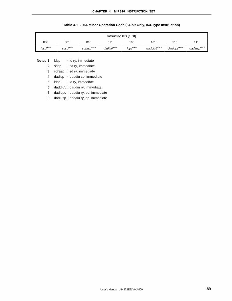
CHAPTER 4 MIPS16 INSTRUCTION SET
User’s Manual U14272EJ1V0UM00 89
Table 4-11. I64 Minor Operation Code (64-bit Only, I64-Type Instruction)
Instruction bits [10:8]
000 001 010 011 100 101 110 111
ldspNote 1 sdspNote 2 sdraspNote 3 dadjspNote 4 ldpcNote 5 daddiu5Note 6 dadiupcNote 7 dadiuspNote 8
Notes 1. ldsp : ld ry, immediate
2. sdsp : sd ry, immediate
3. sdrasp : sd ra, immediate
4. dadjsp : daddiu sp, immediate
5. ldpc : ld ry, immediate
6. daddiu5 : daddiu ry, immediate
7. dadiupc : daddiu ry, pc, immediate
8. dadiusp : daddiu ry, sp, immediate
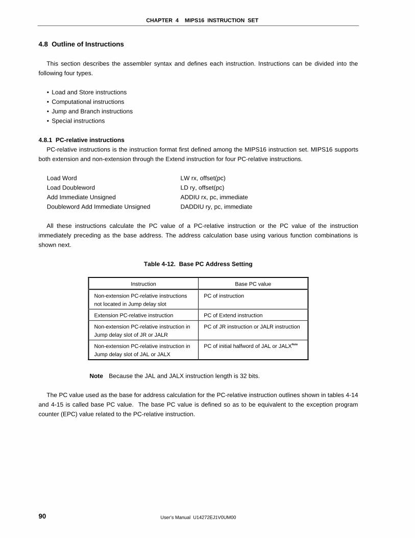
CHAPTER 4 MIPS16 INSTRUCTION SET
User’s Manual U14272EJ1V0UM0090
4.8 Outline of Instructions
This section describes the assembler syntax and defines each instruction. Instructions can be divided into the
following four types.
• Load and Store instructions
• Computational instructions
• Jump and Branch instructions
• Special instructions
4.8.1 PC-relative instructions
PC-relative instructions is the instruction format first defined among the MIPS16 instruction set. MIPS16 supports
both extension and non-extension through the Extend instruction for four PC-relative instructions.
Load Word LW rx, offset(pc)
Load Doubleword LD ry, offset(pc)
Add Immediate Unsigned ADDIU rx, pc, immediate
Doubleword Add Immediate Unsigned DADDIU ry, pc, immediate
All these instructions calculate the PC value of a PC-relative instruction or the PC value of the instruction
immediately preceding as the base address. The address calculation base using various function combinations is
shown next.
Table 4-12. Base PC Address Setting
Instruction Base PC value
Non-extension PC-relative instructions
not located in Jump delay slot
PC of instruction
Extension PC-relative instruction PC of Extend instruction
Non-extension PC-relative instruction in
Jump delay slot of JR or JALR
PC of JR instruction or JALR instruction
Non-extension PC-relative instruction in
Jump delay slot of JAL or JALX
PC of initial halfword of JAL or JALXNote
Note Because the JAL and JALX instruction length is 32 bits.
The PC value used as the base for address calculation for the PC-relative instruction outlines shown in tables 4-14
and 4-15 is called base PC value. The base PC value is defined so as to be equivalent to the exception program
counter (EPC) value related to the PC-relative instruction.
CHAPTER 4 MIPS16 INSTRUCTION SET
User’s Manual U14272EJ1V0UM00 91
4.8.2 Extend instruction
The Extend instruction can extend the immediate fields of MIPS16 instructions, which have fewer immediate fields
than equivalent 32-bit MIPS instructions. The Extend instruction must always precede (by one instruction) the
instruction whose immediate field you want to extend. Every extended instruction consumes four bytes in program
memory instead of two bytes (two bytes for Extend and two bytes for the instruction being extended), and it can cross
a word boundary.
For example, the MIPS16 instruction
lw ry, offset (rx)
contains a five-bit immediate. The immediate expands to 16 bits (000000000offset00) before execution in the
pipeline. This allows 32 different offset values of 0, 4, 8, and up through 124. Once extended, this instruction can hold
any of the normal 65,536 values in the range –32768 through 32767.
Shift instructions are extended to 5-bit unsigned immediate values. All other immediate instructions expand to
either signed or unsigned 16-bit immediate values. The only exceptions are
addiu ry, rx, immediate
daddiu ry, rx, immediate
which can be extended only to a 15-bit signed immediate.
There is only one restriction. Extended instructions should not be placed in jump delay slots. Otherwise, the
results are unpredictable because the pipeline would attempt to execute one half the instruction.
Table 4-13 lists the MIPS16 extendable instructions, the size of their immediate, and how much each immediate
can be extended when preceded with the Extend instruction.
For the instruction format of the Extend instruction, see 4.6 Instruction Format .
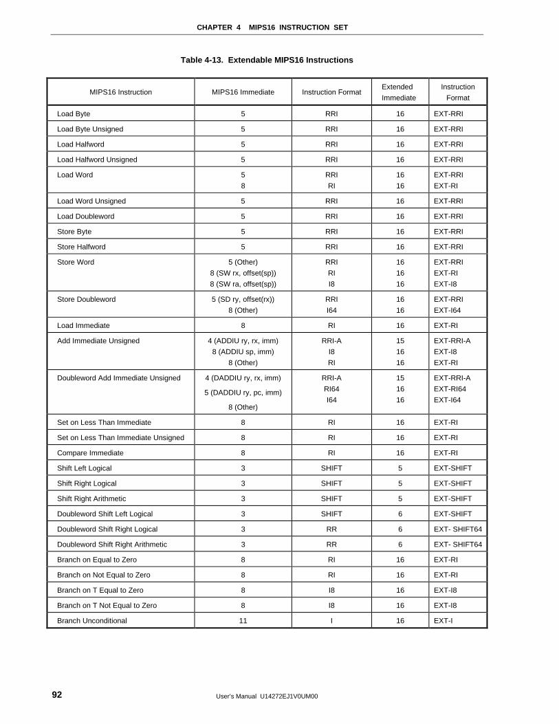
CHAPTER 4 MIPS16 INSTRUCTION SET
User’s Manual U14272EJ1V0UM0092
Table 4-13. Extendable MIPS16 Instructions
MIPS16 Instruction MIPS16 Immediate Instruction FormatExtended
Immediate
Instruction
Format
Load Byte 5 RRI 16 EXT-RRI
Load Byte Unsigned 5 RRI 16 EXT-RRI
Load Halfword 5 RRI 16 EXT-RRI
Load Halfword Unsigned 5 RRI 16 EXT-RRI
Load Word 5
8
RRI
RI
16
16
EXT-RRI
EXT-RI
Load Word Unsigned 5 RRI 16 EXT-RRI
Load Doubleword 5 RRI 16 EXT-RRI
Store Byte 5 RRI 16 EXT-RRI
Store Halfword 5 RRI 16 EXT-RRI
Store Word 5 (Other)
8 (SW rx, offset(sp))
8 (SW ra, offset(sp))
RRI
RI
I8
16
16
16
EXT-RRI
EXT-RI
EXT-I8
Store Doubleword 5 (SD ry, offset(rx))
8 (Other)
RRI
I64
16
16
EXT-RRI
EXT-I64
Load Immediate 8 RI 16 EXT-RI
Add Immediate Unsigned 4 (ADDIU ry, rx, imm)
8 (ADDIU sp, imm)
8 (Other)
RRI-A
I8
RI
15
16
16
EXT-RRI-A
EXT-I8
EXT-RI
Doubleword Add Immediate Unsigned 4 (DADDIU ry, rx, imm)
5 (DADDIU ry, pc, imm)
8 (Other)
RRI-A
RI64
I64
15
16
16
EXT-RRI-A
EXT-RI64
EXT-I64
Set on Less Than Immediate 8 RI 16 EXT-RI
Set on Less Than Immediate Unsigned 8 RI 16 EXT-RI
Compare Immediate 8 RI 16 EXT-RI
Shift Left Logical 3 SHIFT 5 EXT-SHIFT
Shift Right Logical 3 SHIFT 5 EXT-SHIFT
Shift Right Arithmetic 3 SHIFT 5 EXT-SHIFT
Doubleword Shift Left Logical 3 SHIFT 6 EXT-SHIFT
Doubleword Shift Right Logical 3 RR 6 EXT- SHIFT64
Doubleword Shift Right Arithmetic 3 RR 6 EXT- SHIFT64
Branch on Equal to Zero 8 RI 16 EXT-RI
Branch on Not Equal to Zero 8 RI 16 EXT-RI
Branch on T Equal to Zero 8 I8 16 EXT-I8
Branch on T Not Equal to Zero 8 I8 16 EXT-I8
Branch Unconditional 11 I 16 EXT-I
CHAPTER 4 MIPS16 INSTRUCTION SET
User’s Manual U14272EJ1V0UM00 93
4.8.3 Delay slots
MIPS16 instructions normally execute in one cycle. However, some instructions have special requirements that
must be met to assure optimum instruction flow. The instructions include All Load, Branch, and Multiply/Divide
instructions.
(1) Load delay slots
MIPS16 operates with delayed loads. This is similar to the method used by 32-bit MIPS instruction sets. If
another instruction references the load destination register before the load operation is completed, one cycle
occurs automatically. To assure the best performance, the compiler should always schedule load delay slots as
early as possible.
(2) Branch delay slots not supported
Unlike for 32-bit MIPS instructions, there are no branch delay slots for branch instructions in MIPS16. If a branch
is taken, the instruction that immediately follows the branch (instruction corresponding to 32-bit MIPS delay slot)
is cancelled. There are no restrictions on the instruction that follows a branch instruction, and such instruction is
executed only when a branch is not taken. Branches, jumps, and extended instructions are permitted in the
instruction slot after a branch.
(3) Jump delay slots
With MIPS16, there is a delay of one cycle after each jump instruction. The processor executes any instruction in
the jump delay slot before it executes the jump target instruction. Two restrictions apply to any instruction placed
in the jump delay slot:
1. Do not specify a branch or jump in the delay slot.
2. Do not specify an extended instruction (32-bits) in the delay slot. Doing so will make the results
unpredictable.
(4) Multiply and divide scheduling
Multiply and divide latency depends on the hardware implementation. If an MFLO or MFHI instruction references
the Multiply or Divide result registers before the result is ready, the pipeline stalls until the operation is complete
and the result is available. However, to assure the best performance, the compiler should always schedule
Multiply and Divide instructions as early as possible.
MIPS16 requires that all MFHI and MFLO instructions be followed by two instructions that do not write to the HI
or LO registers. Otherwise, the data read by MFLO or MFHI will be undefined. The Extend instruction is counted
singly as one instruction.
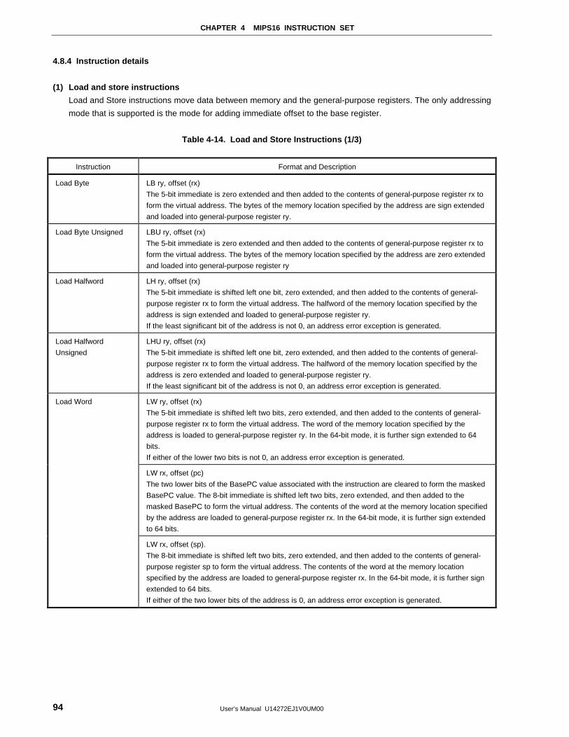
CHAPTER 4 MIPS16 INSTRUCTION SET
User’s Manual U14272EJ1V0UM0094
4.8.4 Instruction details
(1) Load and store instructions
Load and Store instructions move data between memory and the general-purpose registers. The only addressing
mode that is supported is the mode for adding immediate offset to the base register.
Table 4-14. Load and Store Instructions (1/3)
Instruction Format and Description
Load Byte LB ry, offset (rx)
The 5-bit immediate is zero extended and then added to the contents of general-purpose register rx to
form the virtual address. The bytes of the memory location specified by the address are sign extended
and loaded into general-purpose register ry.
Load Byte Unsigned LBU ry, offset (rx)
The 5-bit immediate is zero extended and then added to the contents of general-purpose register rx to
form the virtual address. The bytes of the memory location specified by the address are zero extended
and loaded into general-purpose register ry
Load Halfword LH ry, offset (rx)
The 5-bit immediate is shifted left one bit, zero extended, and then added to the contents of general-
purpose register rx to form the virtual address. The halfword of the memory location specified by the
address is sign extended and loaded to general-purpose register ry.
If the least significant bit of the address is not 0, an address error exception is generated.
Load Halfword
Unsigned
LHU ry, offset (rx)
The 5-bit immediate is shifted left one bit, zero extended, and then added to the contents of general-
purpose register rx to form the virtual address. The halfword of the memory location specified by the
address is zero extended and loaded to general-purpose register ry.
If the least significant bit of the address is not 0, an address error exception is generated.
LW ry, offset (rx)
The 5-bit immediate is shifted left two bits, zero extended, and then added to the contents of general-
purpose register rx to form the virtual address. The word of the memory location specified by the
address is loaded to general-purpose register ry. In the 64-bit mode, it is further sign extended to 64
bits.
If either of the lower two bits is not 0, an address error exception is generated.
LW rx, offset (pc)
The two lower bits of the BasePC value associated with the instruction are cleared to form the masked
BasePC value. The 8-bit immediate is shifted left two bits, zero extended, and then added to the
masked BasePC to form the virtual address. The contents of the word at the memory location specified
by the address are loaded to general-purpose register rx. In the 64-bit mode, it is further sign extended
to 64 bits.
Load Word
LW rx, offset (sp).
The 8-bit immediate is shifted left two bits, zero extended, and then added to the contents of general-
purpose register sp to form the virtual address. The contents of the word at the memory location
specified by the address are loaded to general-purpose register rx. In the 64-bit mode, it is further sign
extended to 64 bits.
If either of the two lower bits of the address is 0, an address error exception is generated.
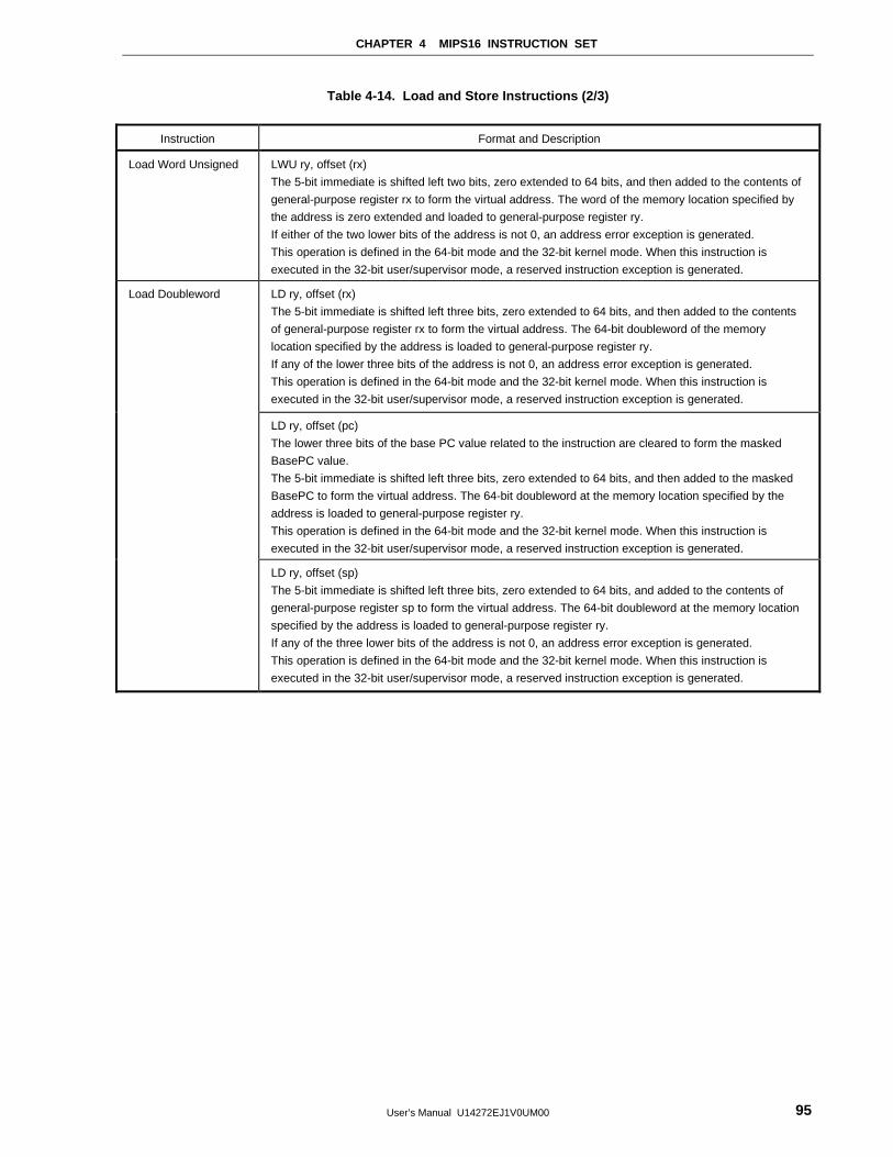
CHAPTER 4 MIPS16 INSTRUCTION SET
User’s Manual U14272EJ1V0UM00 95
Table 4-14. Load and Store Instructions (2/3)
Instruction Format and Description
Load Word Unsigned LWU ry, offset (rx)
The 5-bit immediate is shifted left two bits, zero extended to 64 bits, and then added to the contents of
general-purpose register rx to form the virtual address. The word of the memory location specified by
the address is zero extended and loaded to general-purpose register ry.
If either of the two lower bits of the address is not 0, an address error exception is generated.
This operation is defined in the 64-bit mode and the 32-bit kernel mode. When this instruction is
executed in the 32-bit user/supervisor mode, a reserved instruction exception is generated.
LD ry, offset (rx)
The 5-bit immediate is shifted left three bits, zero extended to 64 bits, and then added to the contents
of general-purpose register rx to form the virtual address. The 64-bit doubleword of the memory
location specified by the address is loaded to general-purpose register ry.
If any of the lower three bits of the address is not 0, an address error exception is generated.
This operation is defined in the 64-bit mode and the 32-bit kernel mode. When this instruction is
executed in the 32-bit user/supervisor mode, a reserved instruction exception is generated.
LD ry, offset (pc)
The lower three bits of the base PC value related to the instruction are cleared to form the masked
BasePC value.
The 5-bit immediate is shifted left three bits, zero extended to 64 bits, and then added to the masked
BasePC to form the virtual address. The 64-bit doubleword at the memory location specified by the
address is loaded to general-purpose register ry.
This operation is defined in the 64-bit mode and the 32-bit kernel mode. When this instruction is
executed in the 32-bit user/supervisor mode, a reserved instruction exception is generated.
Load Doubleword
LD ry, offset (sp)
The 5-bit immediate is shifted left three bits, zero extended to 64 bits, and added to the contents of
general-purpose register sp to form the virtual address. The 64-bit doubleword at the memory location
specified by the address is loaded to general-purpose register ry.
If any of the three lower bits of the address is not 0, an address error exception is generated.
This operation is defined in the 64-bit mode and the 32-bit kernel mode. When this instruction is
executed in the 32-bit user/supervisor mode, a reserved instruction exception is generated.
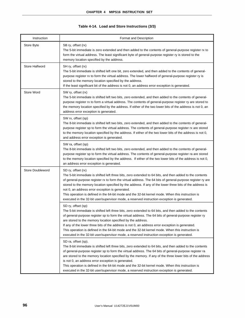
CHAPTER 4 MIPS16 INSTRUCTION SET
User’s Manual U14272EJ1V0UM0096
Table 4-14. Load and Store Instructions (3/3)
Instruction Format and Description
Store Byte SB ry, offset (rx)
The 5-bit immediate is zero extended and then added to the contents of general-purpose register rx to
form the virtual address. The least significant byte of general-purpose register ry is stored to the
memory location specified by the address.
Store Halfword SH ry, offset (rx)
The 5-bit immediate is shifted left one bit, zero extended, and then added to the contents of general-
purpose register rx to form the virtual address. The lower halfword of general-purpose register ry is
stored to the memory location specified by the address.
If the least significant bit of the address is not 0, an address error exception is generated.
SW ry, offset (rx)
The 5-bit immediate is shifted left two bits, zero extended, and then added to the contents of general-
purpose register rx to form a virtual address. The contents of general-purpose register ry are stored to
the memory location specified by the address. If either of the two lower bits of the address is not 0, an
address error exception is generated.
SW rx, offset (sp)
The 8-bit immediate is shifted left two bits, zero extended, and then added to the contents of general-
purpose register sp to form the virtual address. The contents of general-purpose register rx are stored
to the memory location specified by the address. If either of the two lower bits of the address is not 0,
and address error exception is generated.
Store Word
SW ra, offset (sp)
The 8-bit immediate is shifted left two bits, zero extended, and then added to the contents of general-
purpose register sp to form the virtual address. The contents of general-purpose register ra are stored
to the memory location specified by the address. If either of the two lower bits of the address is not 0,
an address error exception is generated.
SD ry, offset (rx)
The 5-bit immediate is shifted left three bits, zero extended to 64 bits, and then added to the contents
of general-purpose register rx to form the virtual address. The 64 bits of general-purpose register ry are
stored to the memory location specified by the address. If any of the lower three bits of the address is
not 0, an address error exception is generated.
This operation is defined in the 64-bit mode and the 32-bit kernel mode. When this instruction is
executed in the 32-bit user/supervisor mode, a reserved instruction exception is generated.
SD ry, offset (sp)
The 5-bit immediate is shifted left three bits, zero extended to 64 bits, and then added to the contents
of general-purpose register sp to form the virtual address. The 64 bits of general-purpose register ry
are stored to the memory location specified by the address.
If any of the lower three bits of the address is not 0, an address error exception is generated.
This operation is defined in the 64-bit mode and the 32-bit kernel mode. When this instruction is
executed in the 32-bit user/supervisor mode, a reserved instruction exception is generated.
Store Doubleword
SD ra, offset (sp).
The 8-bit immediate is shifted left three bits, zero extended to 64 bits, and then added to the contents
of general-purpose register sp to form the virtual address. The 64 bits of general-purpose register ra
are stored to the memory location specified by the memory. If any of the three lower bits of the address
is not 0, an address error exception is generated.
This operation is defined in the 64-bit mode and the 32-bit kernel mode. When this instruction is
executed in the 32-bit user/supervisor mode, a reserved instruction exception is generated.
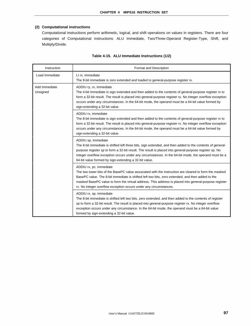
CHAPTER 4 MIPS16 INSTRUCTION SET
User’s Manual U14272EJ1V0UM00 97
(2) Computational instructions
Computational instructions perform arithmetic, logical, and shift operations on values in registers. There are four
categories of Computational instructions: ALU Immediate, Two/Three-Operand Register-Type, Shift, and
Multiply/Divide.
Table 4-15. ALU Immediate Instructions (1/2)
Instruction Format and Description
Load Immediate LI rx, immediate
The 8-bit immediate is zero extended and loaded to general-purpose register rx.
ADDIU ry, rx, immediate
The 4-bit immediate is sign extended and then added to the contents of general-purpose register rx to
form a 32-bit result. The result is placed into general-purpose register ry. No integer overflow exception
occurs under any circumstances. In the 64-bit mode, the operand must be a 64-bit value formed by
sign-extending a 32-bit value.
ADDIU rx, immediate
The 8-bit immediate is sign extended and then added to the contents of general-purpose register rx to
form a 32-bit result. The result is placed into general-purpose register rx. No integer overflow exception
occurs under any circumstances. In the 64-bit mode, the operand must be a 64-bit value formed by
sign-extending a 32-bit value.
ADDIU sp, immediate
The 8-bit immediate is shifted left three bits, sign extended, and then added to the contents of general-
purpose register sp to form a 32-bit result. The result is placed into general-purpose register sp. No
integer overflow exception occurs under any circumstances. In the 64-bit mode, the operand must be a
64-bit value formed by sign-extending a 32-bit value.
ADDIU rx, pc, immediate
The two lower bits of the BasePC value associated with the instruction are cleared to form the masked
BasePC value. The 8-bit immediate is shifted left two bits, zero extended, and then added to the
masked BasePC value to form the virtual address. This address is placed into general-purpose register
rx. No integer overflow exception occurs under any circumstances.
Add Immediate
Unsigned
ADDIU rx, sp, immediate
The 8-bit immediate is shifted left two bits, zero extended, and then added to the contents of register
sp to form a 32-bit result. The result is placed into general-purpose register rx. No integer overflow
exception occurs under any circumstance. In the 64-bit mode, the operand must be a 64-bit value
formed by sign-extending a 32-bit value.
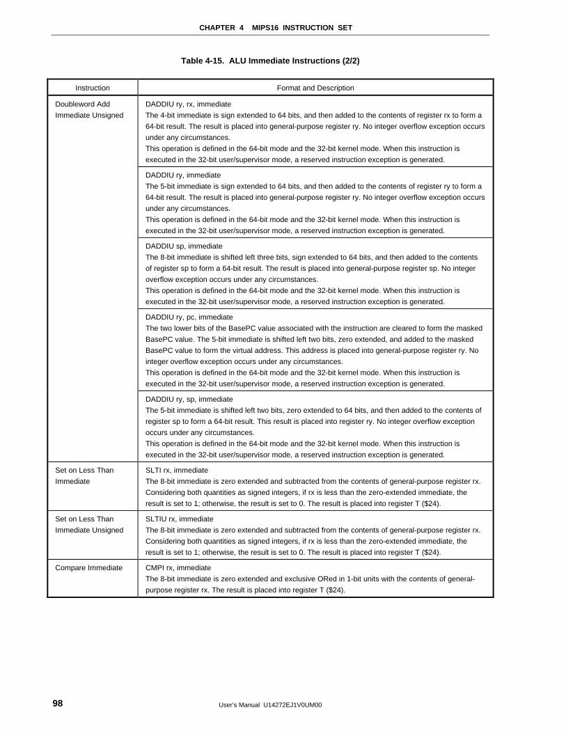
CHAPTER 4 MIPS16 INSTRUCTION SET
User’s Manual U14272EJ1V0UM0098
Table 4-15. ALU Immediate Instructions (2/2)
Instruction Format and Description
DADDIU ry, rx, immediate
The 4-bit immediate is sign extended to 64 bits, and then added to the contents of register rx to form a
64-bit result. The result is placed into general-purpose register ry. No integer overflow exception occurs
under any circumstances.
This operation is defined in the 64-bit mode and the 32-bit kernel mode. When this instruction is
executed in the 32-bit user/supervisor mode, a reserved instruction exception is generated.
DADDIU ry, immediate
The 5-bit immediate is sign extended to 64 bits, and then added to the contents of register ry to form a
64-bit result. The result is placed into general-purpose register ry. No integer overflow exception occurs
under any circumstances.
This operation is defined in the 64-bit mode and the 32-bit kernel mode. When this instruction is
executed in the 32-bit user/supervisor mode, a reserved instruction exception is generated.
DADDIU sp, immediate
The 8-bit immediate is shifted left three bits, sign extended to 64 bits, and then added to the contents
of register sp to form a 64-bit result. The result is placed into general-purpose register sp. No integer
overflow exception occurs under any circumstances.
This operation is defined in the 64-bit mode and the 32-bit kernel mode. When this instruction is
executed in the 32-bit user/supervisor mode, a reserved instruction exception is generated.
DADDIU ry, pc, immediate
The two lower bits of the BasePC value associated with the instruction are cleared to form the masked
BasePC value. The 5-bit immediate is shifted left two bits, zero extended, and added to the masked
BasePC value to form the virtual address. This address is placed into general-purpose register ry. No
integer overflow exception occurs under any circumstances.
This operation is defined in the 64-bit mode and the 32-bit kernel mode. When this instruction is
executed in the 32-bit user/supervisor mode, a reserved instruction exception is generated.
Doubleword Add
Immediate Unsigned
DADDIU ry, sp, immediate
The 5-bit immediate is shifted left two bits, zero extended to 64 bits, and then added to the contents of
register sp to form a 64-bit result. This result is placed into register ry. No integer overflow exception
occurs under any circumstances.
This operation is defined in the 64-bit mode and the 32-bit kernel mode. When this instruction is
executed in the 32-bit user/supervisor mode, a reserved instruction exception is generated.
Set on Less Than
Immediate
SLTI rx, immediate
The 8-bit immediate is zero extended and subtracted from the contents of general-purpose register rx.
Considering both quantities as signed integers, if rx is less than the zero-extended immediate, the
result is set to 1; otherwise, the result is set to 0. The result is placed into register T ($24).
Set on Less Than
Immediate Unsigned
SLTIU rx, immediate
The 8-bit immediate is zero extended and subtracted from the contents of general-purpose register rx.
Considering both quantities as signed integers, if rx is less than the zero-extended immediate, the
result is set to 1; otherwise, the result is set to 0. The result is placed into register T ($24).
Compare Immediate CMPI rx, immediate
The 8-bit immediate is zero extended and exclusive ORed in 1-bit units with the contents of general-
purpose register rx. The result is placed into register T ($24).
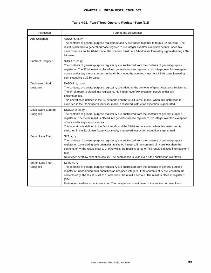
CHAPTER 4 MIPS16 INSTRUCTION SET
User’s Manual U14272EJ1V0UM00 99
Table 4-16. Two-/Three-Operand Register Type (1/2)
Instruction Format and Description
Add Unsigned ADDU rz, rx, ry
The contents of general-purpose registers rx and ry are added together to form a 32-bit result. The
result is placed into general-purpose register rz. No integer overflow exception occurs under any
circumstances. In the 64-bit mode, the operand must be a 64-bit value formed by sign-extending a 32-
bit value.
Subtract Unsigned SUBU rz, rx, ry
The contents of general-purpose register ry are subtracted from the contents of general-purpose
register rx. The 32-bit result is placed into general-purpose register rz. No integer overflow exception
occurs under any circumstances. In the 64-bit mode, the operand must be a 64-bit value formed by
sign-extending a 32-bit value.
Doubleword Add
Unsigned
DADDU rz, rx, ry
The contents of general-purpose register ry are added to the contents of general-purpose register rx.
The 64-bit result is placed into register rz. No integer overflow exception occurs under any
circumstances.
This operation is defined in the 64-bit mode and the 32-bit kernel mode. When this instruction is
executed in the 32-bit user/supervisor mode, a reserved instruction exception is generated.
Doubleword Subtract
Unsigned
DSUBU rz, rx, ry
The contents of general-purpose register ry are subtracted from the contents of general-purpose
register rx. The 64-bit result is placed into general-purpose register rz. No integer overflow exception
occurs under any circumstances.
This operation is defined in the 64-bit mode and the 32-bit kernel mode. When this instruction is
executed in the 32-bit user/supervisor mode, a reserved instruction exception is generated.
Set on Less Than SLT rx, ry
The contents of general-purpose register ry are subtracted from the contents of general-purpose
register rx. Considering both quantities as signed integers, if the contents of rx are less than the
contents of ry, the result is set to 1; otherwise, the result is set to 0. The result is placed into register T
($24).
No integer overflow exception occurs. The comparison is valid even if the subtraction overflows.
Set on Less Than
Unsigned
SLTU rx, ry
The contents of general-purpose register ry are subtracted from the contents of general-purpose
register rx. Considering both quantities as unsigned integers, if the contents of rx are less than the
contents of ry, the result is set to 1; otherwise, the result it set to 0. The result is place in register T
($24).
No integer overflow exception occurs. The comparison is valid even if the subtraction overflows.
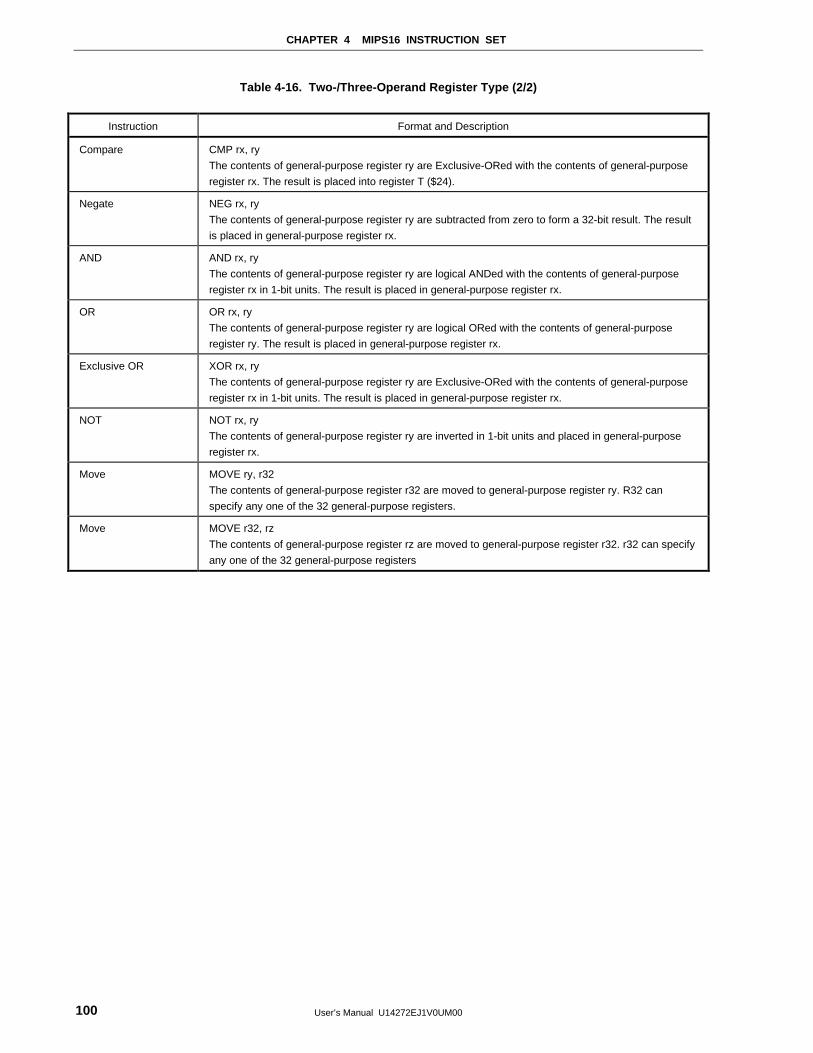
CHAPTER 4 MIPS16 INSTRUCTION SET
User’s Manual U14272EJ1V0UM00100
Table 4-16. Two-/Three-Operand Register Type (2/2)
Instruction Format and Description
Compare CMP rx, ry
The contents of general-purpose register ry are Exclusive-ORed with the contents of general-purpose
register rx. The result is placed into register T ($24).
Negate NEG rx, ry
The contents of general-purpose register ry are subtracted from zero to form a 32-bit result. The result
is placed in general-purpose register rx.
AND AND rx, ry
The contents of general-purpose register ry are logical ANDed with the contents of general-purpose
register rx in 1-bit units. The result is placed in general-purpose register rx.
OR OR rx, ry
The contents of general-purpose register ry are logical ORed with the contents of general-purpose
register ry. The result is placed in general-purpose register rx.
Exclusive OR XOR rx, ry
The contents of general-purpose register ry are Exclusive-ORed with the contents of general-purpose
register rx in 1-bit units. The result is placed in general-purpose register rx.
NOT NOT rx, ry
The contents of general-purpose register ry are inverted in 1-bit units and placed in general-purpose
register rx.
Move MOVE ry, r32
The contents of general-purpose register r32 are moved to general-purpose register ry. R32 can
specify any one of the 32 general-purpose registers.
Move MOVE r32, rz
The contents of general-purpose register rz are moved to general-purpose register r32. r32 can specify
any one of the 32 general-purpose registers
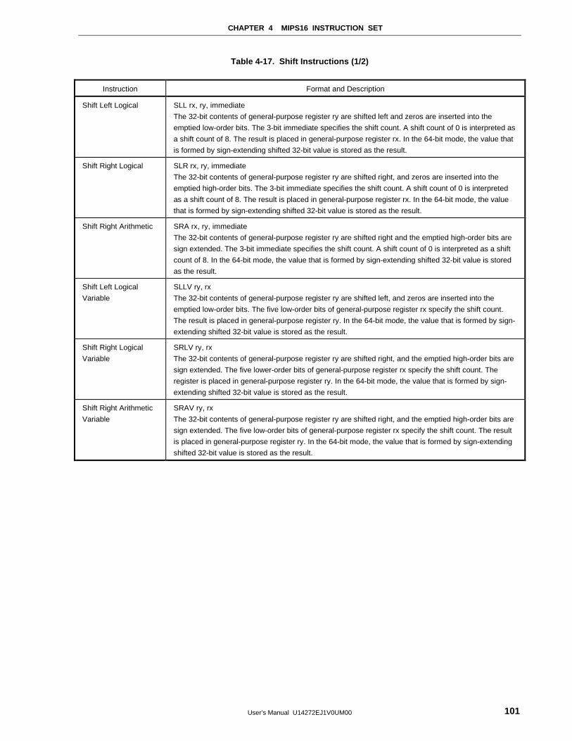
CHAPTER 4 MIPS16 INSTRUCTION SET
User’s Manual U14272EJ1V0UM00 101
Table 4-17. Shift Instructions (1/2)
Instruction Format and Description
Shift Left Logical SLL rx, ry, immediate
The 32-bit contents of general-purpose register ry are shifted left and zeros are inserted into the
emptied low-order bits. The 3-bit immediate specifies the shift count. A shift count of 0 is interpreted as
a shift count of 8. The result is placed in general-purpose register rx. In the 64-bit mode, the value that
is formed by sign-extending shifted 32-bit value is stored as the result.
Shift Right Logical SLR rx, ry, immediate
The 32-bit contents of general-purpose register ry are shifted right, and zeros are inserted into the
emptied high-order bits. The 3-bit immediate specifies the shift count. A shift count of 0 is interpreted
as a shift count of 8. The result is placed in general-purpose register rx. In the 64-bit mode, the value
that is formed by sign-extending shifted 32-bit value is stored as the result.
Shift Right Arithmetic SRA rx, ry, immediate
The 32-bit contents of general-purpose register ry are shifted right and the emptied high-order bits are
sign extended. The 3-bit immediate specifies the shift count. A shift count of 0 is interpreted as a shift
count of 8. In the 64-bit mode, the value that is formed by sign-extending shifted 32-bit value is stored
as the result.
Shift Left Logical
Variable
SLLV ry, rx
The 32-bit contents of general-purpose register ry are shifted left, and zeros are inserted into the
emptied low-order bits. The five low-order bits of general-purpose register rx specify the shift count.
The result is placed in general-purpose register ry. In the 64-bit mode, the value that is formed by sign-
extending shifted 32-bit value is stored as the result.
Shift Right Logical
Variable
SRLV ry, rx
The 32-bit contents of general-purpose register ry are shifted right, and the emptied high-order bits are
sign extended. The five lower-order bits of general-purpose register rx specify the shift count. The
register is placed in general-purpose register ry. In the 64-bit mode, the value that is formed by sign-
extending shifted 32-bit value is stored as the result.
Shift Right Arithmetic
Variable
SRAV ry, rx
The 32-bit contents of general-purpose register ry are shifted right, and the emptied high-order bits are
sign extended. The five low-order bits of general-purpose register rx specify the shift count. The result
is placed in general-purpose register ry. In the 64-bit mode, the value that is formed by sign-extending
shifted 32-bit value is stored as the result.
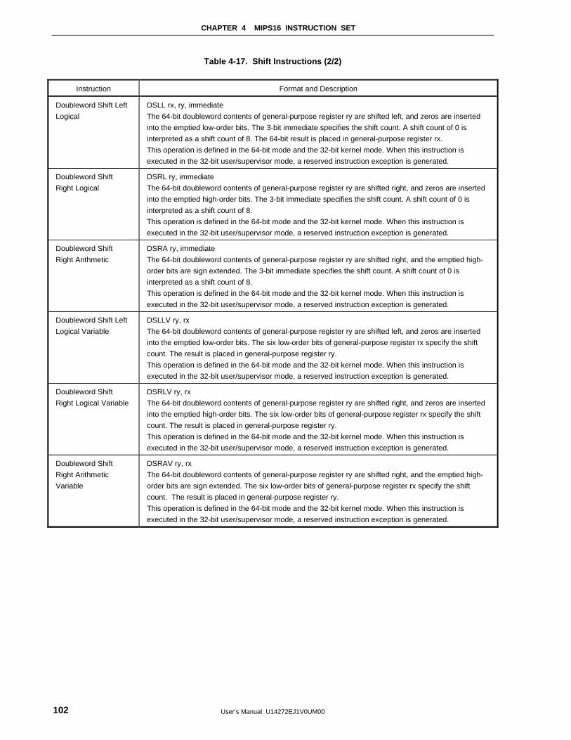
CHAPTER 4 MIPS16 INSTRUCTION SET
User’s Manual U14272EJ1V0UM00102
Table 4-17. Shift Instructions (2/2)
Instruction Format and Description
Doubleword Shift Left
Logical
DSLL rx, ry, immediate
The 64-bit doubleword contents of general-purpose register ry are shifted left, and zeros are inserted
into the emptied low-order bits. The 3-bit immediate specifies the shift count. A shift count of 0 is
interpreted as a shift count of 8. The 64-bit result is placed in general-purpose register rx.
This operation is defined in the 64-bit mode and the 32-bit kernel mode. When this instruction is
executed in the 32-bit user/supervisor mode, a reserved instruction exception is generated.
Doubleword Shift
Right Logical
DSRL ry, immediate
The 64-bit doubleword contents of general-purpose register ry are shifted right, and zeros are inserted
into the emptied high-order bits. The 3-bit immediate specifies the shift count. A shift count of 0 is
interpreted as a shift count of 8.
This operation is defined in the 64-bit mode and the 32-bit kernel mode. When this instruction is
executed in the 32-bit user/supervisor mode, a reserved instruction exception is generated.
Doubleword Shift
Right Arithmetic
DSRA ry, immediate
The 64-bit doubleword contents of general-purpose register ry are shifted right, and the emptied high-
order bits are sign extended. The 3-bit immediate specifies the shift count. A shift count of 0 is
interpreted as a shift count of 8.
This operation is defined in the 64-bit mode and the 32-bit kernel mode. When this instruction is
executed in the 32-bit user/supervisor mode, a reserved instruction exception is generated.
Doubleword Shift Left
Logical Variable
DSLLV ry, rx
The 64-bit doubleword contents of general-purpose register ry are shifted left, and zeros are inserted
into the emptied low-order bits. The six low-order bits of general-purpose register rx specify the shift
count. The result is placed in general-purpose register ry.
This operation is defined in the 64-bit mode and the 32-bit kernel mode. When this instruction is
executed in the 32-bit user/supervisor mode, a reserved instruction exception is generated.
Doubleword Shift
Right Logical Variable
DSRLV ry, rx
The 64-bit doubleword contents of general-purpose register ry are shifted right, and zeros are inserted
into the emptied high-order bits. The six low-order bits of general-purpose register rx specify the shift
count. The result is placed in general-purpose register ry.
This operation is defined in the 64-bit mode and the 32-bit kernel mode. When this instruction is
executed in the 32-bit user/supervisor mode, a reserved instruction exception is generated.
Doubleword Shift
Right Arithmetic
Variable
DSRAV ry, rx
The 64-bit doubleword contents of general-purpose register ry are shifted right, and the emptied high-
order bits are sign extended. The six low-order bits of general-purpose register rx specify the shift
count. The result is placed in general-purpose register ry.
This operation is defined in the 64-bit mode and the 32-bit kernel mode. When this instruction is
executed in the 32-bit user/supervisor mode, a reserved instruction exception is generated.
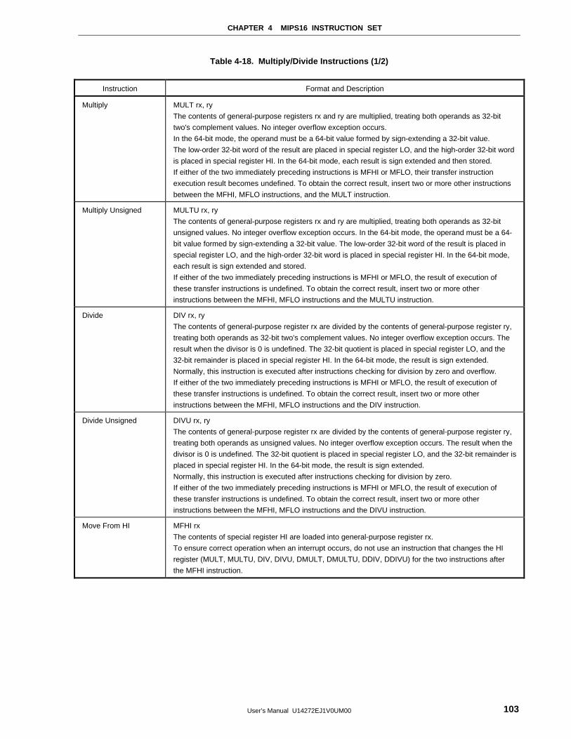
CHAPTER 4 MIPS16 INSTRUCTION SET
User’s Manual U14272EJ1V0UM00 103
Table 4-18. Multiply/Divide Instructions (1/2)
Instruction Format and Description
Multiply MULT rx, ry
The contents of general-purpose registers rx and ry are multiplied, treating both operands as 32-bit
two's complement values. No integer overflow exception occurs.
In the 64-bit mode, the operand must be a 64-bit value formed by sign-extending a 32-bit value.
The low-order 32-bit word of the result are placed in special register LO, and the high-order 32-bit word
is placed in special register HI. In the 64-bit mode, each result is sign extended and then stored.
If either of the two immediately preceding instructions is MFHI or MFLO, their transfer instruction
execution result becomes undefined. To obtain the correct result, insert two or more other instructions
between the MFHI, MFLO instructions, and the MULT instruction.
Multiply Unsigned MULTU rx, ry
The contents of general-purpose registers rx and ry are multiplied, treating both operands as 32-bit
unsigned values. No integer overflow exception occurs. In the 64-bit mode, the operand must be a 64-
bit value formed by sign-extending a 32-bit value. The low-order 32-bit word of the result is placed in
special register LO, and the high-order 32-bit word is placed in special register HI. In the 64-bit mode,
each result is sign extended and stored.
If either of the two immediately preceding instructions is MFHI or MFLO, the result of execution of
these transfer instructions is undefined. To obtain the correct result, insert two or more other
instructions between the MFHI, MFLO instructions and the MULTU instruction.
Divide DIV rx, ry
The contents of general-purpose register rx are divided by the contents of general-purpose register ry,
treating both operands as 32-bit two's complement values. No integer overflow exception occurs. The
result when the divisor is 0 is undefined. The 32-bit quotient is placed in special register LO, and the
32-bit remainder is placed in special register HI. In the 64-bit mode, the result is sign extended.
Normally, this instruction is executed after instructions checking for division by zero and overflow.
If either of the two immediately preceding instructions is MFHI or MFLO, the result of execution of
these transfer instructions is undefined. To obtain the correct result, insert two or more other
instructions between the MFHI, MFLO instructions and the DIV instruction.
Divide Unsigned DIVU rx, ry
The contents of general-purpose register rx are divided by the contents of general-purpose register ry,
treating both operands as unsigned values. No integer overflow exception occurs. The result when the
divisor is 0 is undefined. The 32-bit quotient is placed in special register LO, and the 32-bit remainder is
placed in special register HI. In the 64-bit mode, the result is sign extended.
Normally, this instruction is executed after instructions checking for division by zero.
If either of the two immediately preceding instructions is MFHI or MFLO, the result of execution of
these transfer instructions is undefined. To obtain the correct result, insert two or more other
instructions between the MFHI, MFLO instructions and the DIVU instruction.
Move From HI MFHI rx
The contents of special register HI are loaded into general-purpose register rx.
To ensure correct operation when an interrupt occurs, do not use an instruction that changes the HI
register (MULT, MULTU, DIV, DIVU, DMULT, DMULTU, DDIV, DDIVU) for the two instructions after
the MFHI instruction.
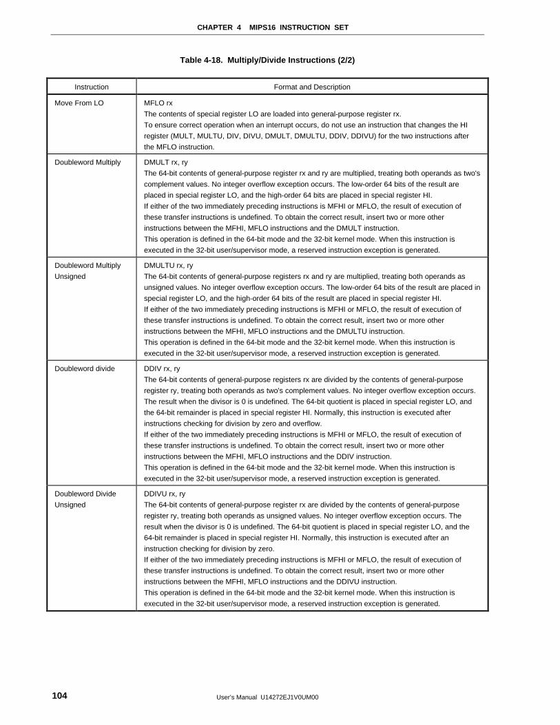
CHAPTER 4 MIPS16 INSTRUCTION SET
User’s Manual U14272EJ1V0UM00104
Table 4-18. Multiply/Divide Instructions (2/2)
Instruction Format and Description
Move From LO MFLO rx
The contents of special register LO are loaded into general-purpose register rx.
To ensure correct operation when an interrupt occurs, do not use an instruction that changes the HI
register (MULT, MULTU, DIV, DIVU, DMULT, DMULTU, DDIV, DDIVU) for the two instructions after
the MFLO instruction.
Doubleword Multiply DMULT rx, ry
The 64-bit contents of general-purpose register rx and ry are multiplied, treating both operands as two's
complement values. No integer overflow exception occurs. The low-order 64 bits of the result are
placed in special register LO, and the high-order 64 bits are placed in special register HI.
If either of the two immediately preceding instructions is MFHI or MFLO, the result of execution of
these transfer instructions is undefined. To obtain the correct result, insert two or more other
instructions between the MFHI, MFLO instructions and the DMULT instruction.
This operation is defined in the 64-bit mode and the 32-bit kernel mode. When this instruction is
executed in the 32-bit user/supervisor mode, a reserved instruction exception is generated.
Doubleword Multiply
Unsigned
DMULTU rx, ry
The 64-bit contents of general-purpose registers rx and ry are multiplied, treating both operands as
unsigned values. No integer overflow exception occurs. The low-order 64 bits of the result are placed in
special register LO, and the high-order 64 bits of the result are placed in special register HI.
If either of the two immediately preceding instructions is MFHI or MFLO, the result of execution of
these transfer instructions is undefined. To obtain the correct result, insert two or more other
instructions between the MFHI, MFLO instructions and the DMULTU instruction.
This operation is defined in the 64-bit mode and the 32-bit kernel mode. When this instruction is
executed in the 32-bit user/supervisor mode, a reserved instruction exception is generated.
Doubleword divide DDIV rx, ry
The 64-bit contents of general-purpose registers rx are divided by the contents of general-purpose
register ry, treating both operands as two's complement values. No integer overflow exception occurs.
The result when the divisor is 0 is undefined. The 64-bit quotient is placed in special register LO, and
the 64-bit remainder is placed in special register HI. Normally, this instruction is executed after
instructions checking for division by zero and overflow.
If either of the two immediately preceding instructions is MFHI or MFLO, the result of execution of
these transfer instructions is undefined. To obtain the correct result, insert two or more other
instructions between the MFHI, MFLO instructions and the DDIV instruction.
This operation is defined in the 64-bit mode and the 32-bit kernel mode. When this instruction is
executed in the 32-bit user/supervisor mode, a reserved instruction exception is generated.
Doubleword Divide
Unsigned
DDIVU rx, ry
The 64-bit contents of general-purpose register rx are divided by the contents of general-purpose
register ry, treating both operands as unsigned values. No integer overflow exception occurs. The
result when the divisor is 0 is undefined. The 64-bit quotient is placed in special register LO, and the
64-bit remainder is placed in special register HI. Normally, this instruction is executed after an
instruction checking for division by zero.
If either of the two immediately preceding instructions is MFHI or MFLO, the result of execution of
these transfer instructions is undefined. To obtain the correct result, insert two or more other
instructions between the MFHI, MFLO instructions and the DDIVU instruction.
This operation is defined in the 64-bit mode and the 32-bit kernel mode. When this instruction is
executed in the 32-bit user/supervisor mode, a reserved instruction exception is generated.
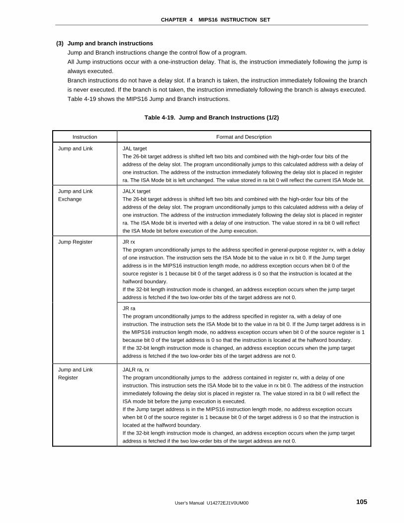
CHAPTER 4 MIPS16 INSTRUCTION SET
User’s Manual U14272EJ1V0UM00 105
(3) Jump and branch instructions
Jump and Branch instructions change the control flow of a program.
All Jump instructions occur with a one-instruction delay. That is, the instruction immediately following the jump is
always executed.
Branch instructions do not have a delay slot. If a branch is taken, the instruction immediately following the branch
is never executed. If the branch is not taken, the instruction immediately following the branch is always executed.
Table 4-19 shows the MIPS16 Jump and Branch instructions.
Table 4-19. Jump and Branch Instructions (1/2)
Instruction Format and Description
Jump and Link JAL target
The 26-bit target address is shifted left two bits and combined with the high-order four bits of the
address of the delay slot. The program unconditionally jumps to this calculated address with a delay of
one instruction. The address of the instruction immediately following the delay slot is placed in register
ra. The ISA Mode bit is left unchanged. The value stored in ra bit 0 will reflect the current ISA Mode bit.
Jump and Link
Exchange
JALX target
The 26-bit target address is shifted left two bits and combined with the high-order four bits of the
address of the delay slot. The program unconditionally jumps to this calculated address with a delay of
one instruction. The address of the instruction immediately following the delay slot is placed in register
ra. The ISA Mode bit is inverted with a delay of one instruction. The value stored in ra bit 0 will reflect
the ISA Mode bit before execution of the Jump execution.
JR rx
The program unconditionally jumps to the address specified in general-purpose register rx, with a delay
of one instruction. The instruction sets the ISA Mode bit to the value in rx bit 0. If the Jump target
address is in the MIPS16 instruction length mode, no address exception occurs when bit 0 of the
source register is 1 because bit 0 of the target address is 0 so that the instruction is located at the
halfword boundary.
If the 32-bit length instruction mode is changed, an address exception occurs when the jump target
address is fetched if the two low-order bits of the target address are not 0.
Jump Register
JR ra
The program unconditionally jumps to the address specified in register ra, with a delay of one
instruction. The instruction sets the ISA Mode bit to the value in ra bit 0. If the Jump target address is in
the MIPS16 instruction length mode, no address exception occurs when bit 0 of the source register is 1
because bit 0 of the target address is 0 so that the instruction is located at the halfword boundary.
If the 32-bit length instruction mode is changed, an address exception occurs when the jump target
address is fetched if the two low-order bits of the target address are not 0.
Jump and Link
Register
JALR ra, rx
The program unconditionally jumps to the address contained in register rx, with a delay of one
instruction. This instruction sets the ISA Mode bit to the value in rx bit 0. The address of the instruction
immediately following the delay slot is placed in register ra. The value stored in ra bit 0 will reflect the
ISA mode bit before the jump execution is executed.
If the Jump target address is in the MIPS16 instruction length mode, no address exception occurs
when bit 0 of the source register is 1 because bit 0 of the target address is 0 so that the instruction is
located at the halfword boundary.
If the 32-bit length instruction mode is changed, an address exception occurs when the jump target
address is fetched if the two low-order bits of the target address are not 0.
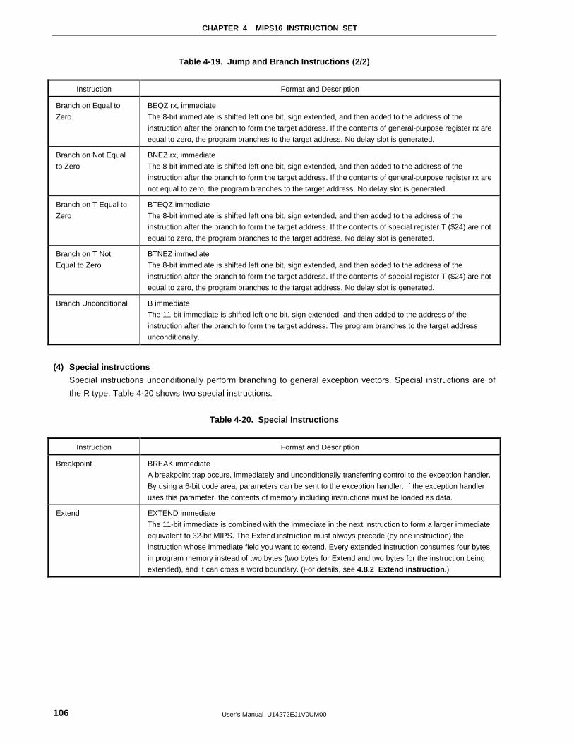
CHAPTER 4 MIPS16 INSTRUCTION SET
User’s Manual U14272EJ1V0UM00106
Table 4-19. Jump and Branch Instructions (2/2)
Instruction Format and Description
Branch on Equal to
Zero
BEQZ rx, immediate
The 8-bit immediate is shifted left one bit, sign extended, and then added to the address of the
instruction after the branch to form the target address. If the contents of general-purpose register rx are
equal to zero, the program branches to the target address. No delay slot is generated.
Branch on Not Equal
to Zero
BNEZ rx, immediate
The 8-bit immediate is shifted left one bit, sign extended, and then added to the address of the
instruction after the branch to form the target address. If the contents of general-purpose register rx are
not equal to zero, the program branches to the target address. No delay slot is generated.
Branch on T Equal to
Zero
BTEQZ immediate
The 8-bit immediate is shifted left one bit, sign extended, and then added to the address of the
instruction after the branch to form the target address. If the contents of special register T ($24) are not
equal to zero, the program branches to the target address. No delay slot is generated.
Branch on T Not
Equal to Zero
BTNEZ immediate
The 8-bit immediate is shifted left one bit, sign extended, and then added to the address of the
instruction after the branch to form the target address. If the contents of special register T ($24) are not
equal to zero, the program branches to the target address. No delay slot is generated.
Branch Unconditional B immediate
The 11-bit immediate is shifted left one bit, sign extended, and then added to the address of the
instruction after the branch to form the target address. The program branches to the target address
unconditionally.
(4) Special instructions
Special instructions unconditionally perform branching to general exception vectors. Special instructions are of
the R type. Table 4-20 shows two special instructions.
Table 4-20. Special Instructions
Instruction Format and Description
Breakpoint BREAK immediate
A breakpoint trap occurs, immediately and unconditionally transferring control to the exception handler.
By using a 6-bit code area, parameters can be sent to the exception handler. If the exception handler
uses this parameter, the contents of memory including instructions must be loaded as data.
Extend EXTEND immediate
The 11-bit immediate is combined with the immediate in the next instruction to form a larger immediate
equivalent to 32-bit MIPS. The Extend instruction must always precede (by one instruction) the
instruction whose immediate field you want to extend. Every extended instruction consumes four bytes
in program memory instead of two bytes (two bytes for Extend and two bytes for the instruction being
extended), and it can cross a word boundary. (For details, see 4.8.2 Extend instruction. )
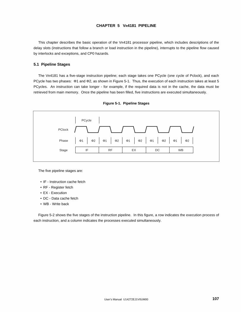
User’s Manual U14272EJ1V0UM00 107
CHAPTER 5 VR4181 PIPELINE
This chapter describes the basic operation of the VR4181 processor pipeline, which includes descriptions of the
delay slots (instructions that follow a branch or load instruction in the pipeline), interrupts to the pipeline flow caused
by interlocks and exceptions, and CP0 hazards.
5.1 Pipeline Stages
The VR4181 has a five-stage instruction pipeline; each stage takes one PCycle (one cycle of Pclock), and each
PCycle has two phases: Φ1 and Φ2, as shown in Figure 5-1. Thus, the execution of each instruction takes at least 5
PCycles. An instruction can take longer - for example, if the required data is not in the cache, the data must be
retrieved from main memory. Once the pipeline has been filled, five instructions are executed simultaneously.
Figure 5-1. Pipeline Stages
Φ1
PCycle
PClock
Stage
Phase
IF RF EX DC WB
Φ2 Φ1 Φ2 Φ1 Φ2 Φ1 Φ2 Φ1 Φ2
The five pipeline stages are:
• IF - Instruction cache fetch
• RF - Register fetch
• EX - Execution
• DC - Data cache fetch
• WB - Write back
Figure 5-2 shows the five stages of the instruction pipeline. In this figure, a row indicates the execution process of
each instruction, and a column indicates the processes executed simultaneously.
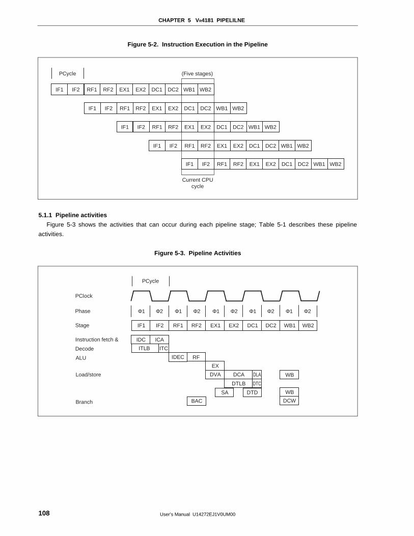
CHAPTER 5 VR4181 PIPELILNE
User’s Manual U14272EJ1V0UM00108
Figure 5-2. Instruction Execution in the Pipeline
(Five stages)
Current CPUcycle
PCycle
RF1 EX1 DC1 WB1IF1 RF2 EX2 DC2 WB2IF2
RF1 EX1 DC1 WB1IF1 RF2 EX2 DC2 WB2IF2
RF1 EX1 DC1 WB1IF1 RF2 EX2 DC2 WB2IF2
RF1 EX1 DC1 WB1IF1 RF2 EX2 DC2 WB2IF2
RF1 EX1 DC1 WB1IF1 RF2 EX2 DC2 WB2IF2
5.1.1 Pipeline activities
Figure 5-3 shows the activities that can occur during each pipeline stage; Table 5-1 describes these pipeline
activities.
Figure 5-3. Pipeline Activities
ALU
Load/store
Branch
IF1
PCycle
PClock
Stage
Instruction fetch &
Decode ITC
ICAIDC
IDEC
WB
EX
RF
ITLB
DCADVA
DTLB
DLA
DTC
WBSA DTD
DCWBAC
RF1 EX1 DC1 WB1IF2 RF2 EX2 DC2 WB2
Φ1Phase Φ2 Φ1 Φ2 Φ1 Φ2 Φ1 Φ2 Φ1 Φ2
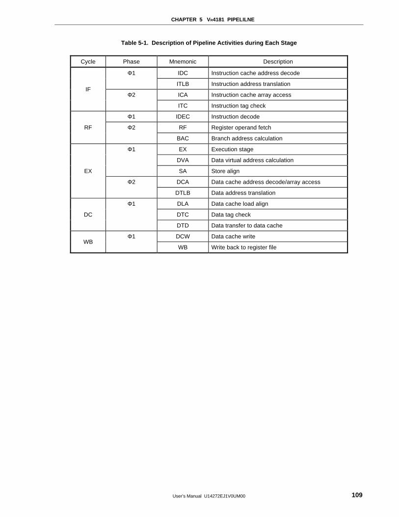
CHAPTER 5 VR4181 PIPELILNE
User’s Manual U14272EJ1V0UM00 109
Table 5-1. Description of Pipeline Activities during Each Stage
Cycle Phase Mnemonic Description
IDC Instruction cache address decodeΦ1
ITLB Instruction address translation
ICA Instruction cache array accessIF
Φ2
ITC Instruction tag check
Φ1 IDEC Instruction decode
RF Register operand fetchRF Φ2
BAC Branch address calculation
EX Execution stage
DVA Data virtual address calculation
Φ1
SA Store align
DCA Data cache address decode/array access
EX
Φ2
DTLB Data address translation
DLA Data cache load align
DTC Data tag checkDC
Φ1
DTD Data transfer to data cache
DCW Data cache writeWB
Φ1
WB Write back to register file
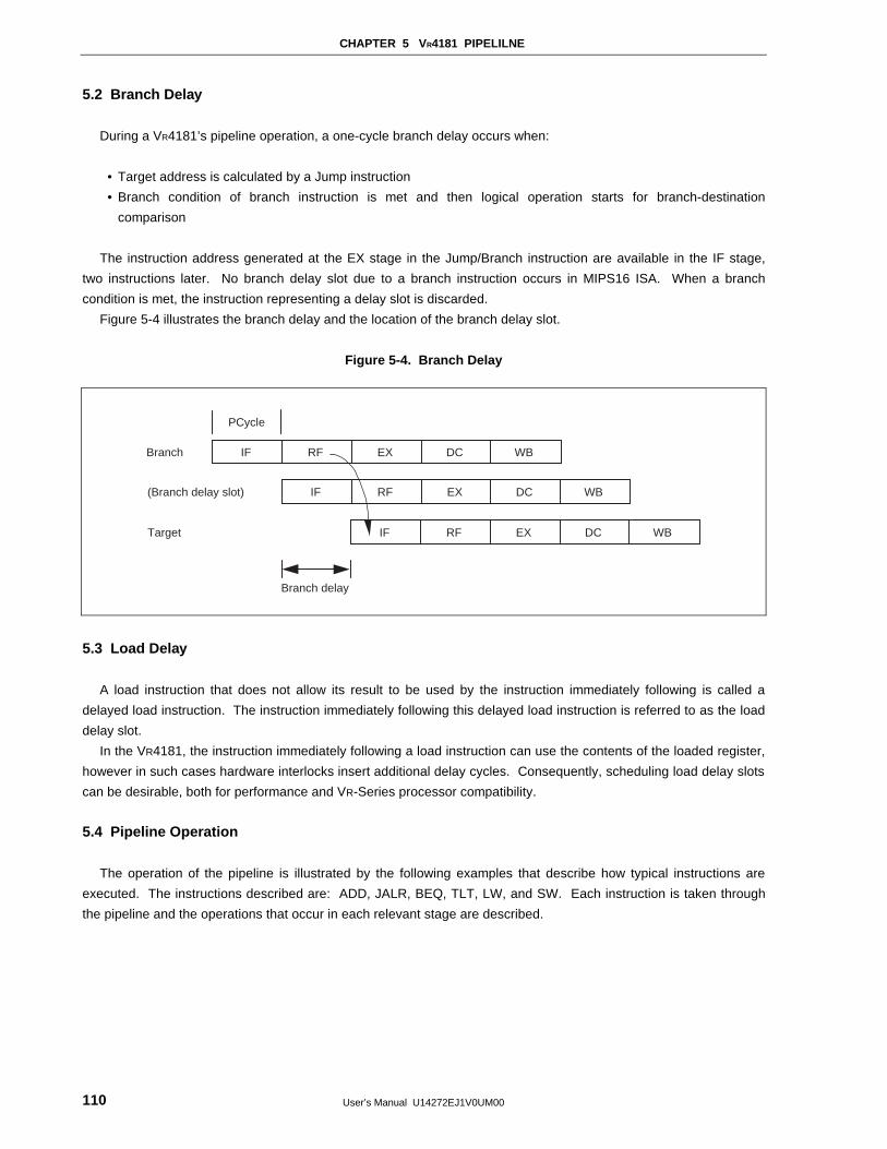
CHAPTER 5 VR4181 PIPELILNE
User’s Manual U14272EJ1V0UM00110
5.2 Branch Delay
During a VR4181’s pipeline operation, a one-cycle branch delay occurs when:
• Target address is calculated by a Jump instruction
• Branch condition of branch instruction is met and then logical operation starts for branch-destination
comparison
The instruction address generated at the EX stage in the Jump/Branch instruction are available in the IF stage,
two instructions later. No branch delay slot due to a branch instruction occurs in MIPS16 ISA. When a branch
condition is met, the instruction representing a delay slot is discarded.
Figure 5-4 illustrates the branch delay and the location of the branch delay slot.
Figure 5-4. Branch Delay
PCycle
IF RF EX DC WB
IFTarget RF EX DC WB
IF
Branch
Branch delay
(Branch delay slot) RF EX DC WB
5.3 Load Delay
A load instruction that does not allow its result to be used by the instruction immediately following is called a
delayed load instruction. The instruction immediately following this delayed load instruction is referred to as the load
delay slot.
In the VR4181, the instruction immediately following a load instruction can use the contents of the loaded register,
however in such cases hardware interlocks insert additional delay cycles. Consequently, scheduling load delay slots
can be desirable, both for performance and VR-Series processor compatibility.
5.4 Pipeline Operation
The operation of the pipeline is illustrated by the following examples that describe how typical instructions are
executed. The instructions described are: ADD, JALR, BEQ, TLT, LW, and SW. Each instruction is taken through
the pipeline and the operations that occur in each relevant stage are described.
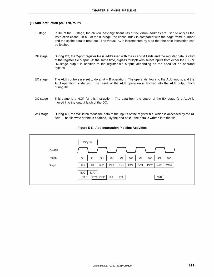
CHAPTER 5 VR4181 PIPELILNE
User’s Manual U14272EJ1V0UM00 111
(1) Add instruction (ADD rd, rs, rt)
IF stage In Φ1 of the IF stage, the eleven least-significant bits of the virtual address are used to access theinstruction cache. In Φ2 of the IF stage, the cache index is compared with the page frame numberand the cache data is read out. The virtual PC is incremented by 4 so that the next instruction canbe fetched.
RF stage During Φ2, the 2-port register file is addressed with the rs and rt fields and the register data is validat the register file output. At the same time, bypass multiplexers select inputs from either the EX- orDC-stage output in addition to the register file output, depending on the need for an operandbypass.
EX stage The ALU controls are set to do an A + B operation. The operands flow into the ALU inputs, and theALU operation is started. The result of the ALU operation is latched into the ALU output latchduring Φ1.
DC stage This stage is a NOP for this instruction. The data from the output of the EX stage (the ALU) ismoved into the output latch of the DC.
WB stage During Φ1, the WB latch feeds the data to the inputs of the register file, which is accessed by the rdfield. The file write strobe is enabled. By the end of Φ1, the data is written into the file.
Figure 5-5. Add Instruction Pipeline Activities
IF1
PCycle
PClock
Stage
ITC
ICAIDC
IDEC WBEXRFITLB
RF1 EX1 DC1 WB1IF2 RF2 EX2 DC2 WB2
Φ1Phase Φ2 Φ1 Φ2 Φ1 Φ2 Φ1 Φ2 Φ1 Φ2
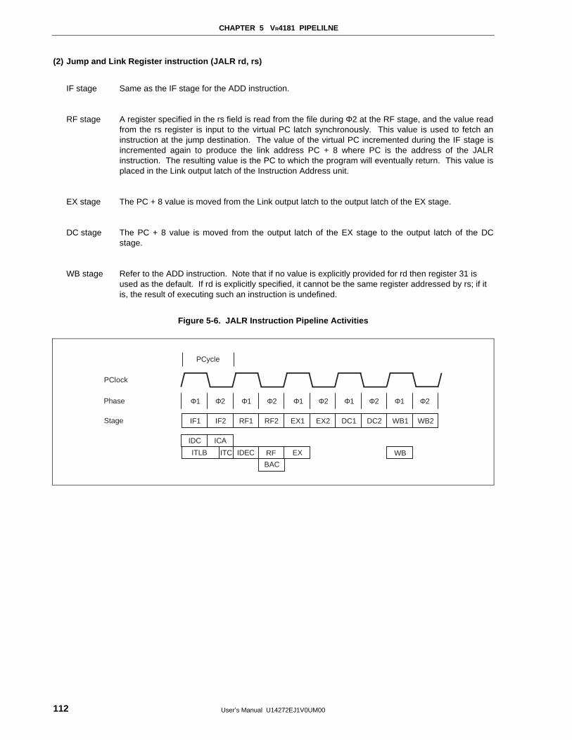
CHAPTER 5 VR4181 PIPELILNE
User’s Manual U14272EJ1V0UM00112
(2) Jump and Link Register instruction (JALR rd, rs)
IF stage Same as the IF stage for the ADD instruction.
RF stage A register specified in the rs field is read from the file during Φ2 at the RF stage, and the value readfrom the rs register is input to the virtual PC latch synchronously. This value is used to fetch aninstruction at the jump destination. The value of the virtual PC incremented during the IF stage isincremented again to produce the link address PC + 8 where PC is the address of the JALRinstruction. The resulting value is the PC to which the program will eventually return. This value isplaced in the Link output latch of the Instruction Address unit.
EX stage The PC + 8 value is moved from the Link output latch to the output latch of the EX stage.
DC stage The PC + 8 value is moved from the output latch of the EX stage to the output latch of the DCstage.
WB stage Refer to the ADD instruction. Note that if no value is explicitly provided for rd then register 31 isused as the default. If rd is explicitly specified, it cannot be the same register addressed by rs; if itis, the result of executing such an instruction is undefined.
Figure 5-6. JALR Instruction Pipeline Activities
IF1
PCycle
PClock
Stage
ITC
ICAIDC
IDEC WBEXRFITLB
BAC
RF1 EX1 DC1 WB1IF2 RF2 EX2 DC2 WB2
Φ1Phase Φ2 Φ1 Φ2 Φ1 Φ2 Φ1 Φ2 Φ1 Φ2
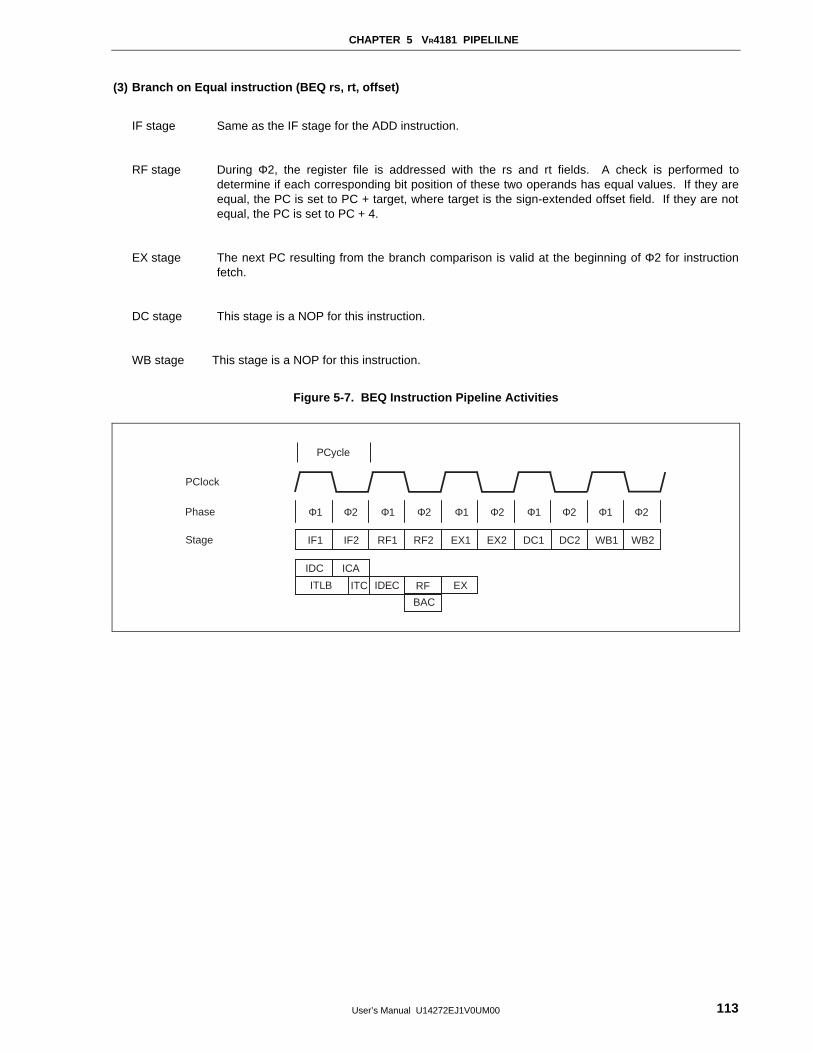
CHAPTER 5 VR4181 PIPELILNE
User’s Manual U14272EJ1V0UM00 113
(3) Branch on Equal instruction (BEQ rs, rt, offset)
IF stage Same as the IF stage for the ADD instruction.
RF stage During Φ2, the register file is addressed with the rs and rt fields. A check is performed todetermine if each corresponding bit position of these two operands has equal values. If they areequal, the PC is set to PC + target, where target is the sign-extended offset field. If they are notequal, the PC is set to PC + 4.
EX stage The next PC resulting from the branch comparison is valid at the beginning of Φ2 for instructionfetch.
DC stage This stage is a NOP for this instruction.
WB stage This stage is a NOP for this instruction.
Figure 5-7. BEQ Instruction Pipeline Activities
IF1
PCycle
PClock
Stage
ITC
ICAIDC
IDEC EXRFITLB
BAC
RF1 EX1 DC1 WB1IF2 RF2 EX2 DC2 WB2
Φ1Phase Φ2 Φ1 Φ2 Φ1 Φ2 Φ1 Φ2 Φ1 Φ2
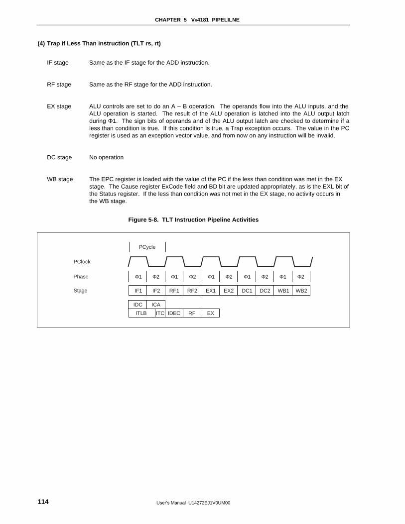
CHAPTER 5 VR4181 PIPELILNE
User’s Manual U14272EJ1V0UM00114
(4) Trap if Less Than instruction (TLT rs, rt)
IF stage Same as the IF stage for the ADD instruction.
RF stage Same as the RF stage for the ADD instruction.
EX stage ALU controls are set to do an A – B operation. The operands flow into the ALU inputs, and theALU operation is started. The result of the ALU operation is latched into the ALU output latchduring Φ1. The sign bits of operands and of the ALU output latch are checked to determine if aless than condition is true. If this condition is true, a Trap exception occurs. The value in the PCregister is used as an exception vector value, and from now on any instruction will be invalid.
DC stage No operation
WB stage The EPC register is loaded with the value of the PC if the less than condition was met in the EXstage. The Cause register ExCode field and BD bit are updated appropriately, as is the EXL bit ofthe Status register. If the less than condition was not met in the EX stage, no activity occurs inthe WB stage.
Figure 5-8. TLT Instruction Pipeline Activities
IF1
PCycle
PClock
Stage
ITC
ICAIDC
IDEC EXRFITLB
RF1 EX1 DC1 WB1IF2 RF2 EX2 DC2 WB2
Φ1Phase Φ2 Φ1 Φ2 Φ1 Φ2 Φ1 Φ2 Φ1 Φ2
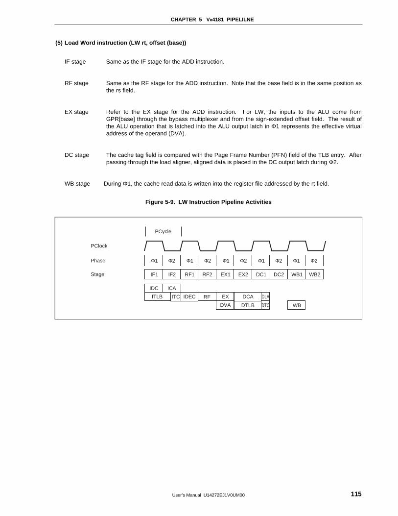
CHAPTER 5 VR4181 PIPELILNE
User’s Manual U14272EJ1V0UM00 115
(5) Load Word instruction (LW rt, offset (base))
IF stage Same as the IF stage for the ADD instruction.
RF stage Same as the RF stage for the ADD instruction. Note that the base field is in the same position asthe rs field.
EX stage Refer to the EX stage for the ADD instruction. For LW, the inputs to the ALU come fromGPR[base] through the bypass multiplexer and from the sign-extended offset field. The result ofthe ALU operation that is latched into the ALU output latch in Φ1 represents the effective virtualaddress of the operand (DVA).
DC stage The cache tag field is compared with the Page Frame Number (PFN) field of the TLB entry. Afterpassing through the load aligner, aligned data is placed in the DC output latch during Φ2.
WB stage During Φ1, the cache read data is written into the register file addressed by the rt field.
Figure 5-9. LW Instruction Pipeline Activities
IF1
PCycle
PClock
Stage
ITC
ICAIDC
IDEC
WB
EXRFITLB DCA
DVA DTLB
DLA
DTC
RF1 EX1 DC1 WB1IF2 RF2 EX2 DC2 WB2
Φ1Phase Φ2 Φ1 Φ2 Φ1 Φ2 Φ1 Φ2 Φ1 Φ2
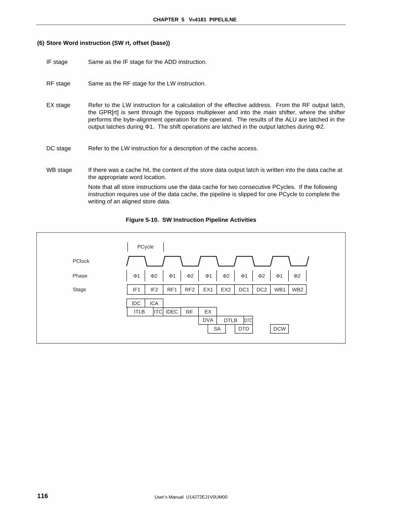
CHAPTER 5 VR4181 PIPELILNE
User’s Manual U14272EJ1V0UM00116
(6) Store Word instruction (SW rt, offset (base))
IF stage Same as the IF stage for the ADD instruction.
RF stage Same as the RF stage for the LW instruction.
EX stage Refer to the LW instruction for a calculation of the effective address. From the RF output latch,the GPR[rt] is sent through the bypass multiplexer and into the main shifter, where the shifterperforms the byte-alignment operation for the operand. The results of the ALU are latched in theoutput latches during Φ1. The shift operations are latched in the output latches during Φ2.
DC stage Refer to the LW instruction for a description of the cache access.
WB stage If there was a cache hit, the content of the store data output latch is written into the data cache atthe appropriate word location.
Note that all store instructions use the data cache for two consecutive PCycles. If the followinginstruction requires use of the data cache, the pipeline is slipped for one PCycle to complete thewriting of an aligned store data.
Figure 5-10. SW Instruction Pipeline Activities
IF1
PCycle
PClock
Stage
ITC
ICAIDC
IDEC EXRFITLB
DVA DTLB DTC
SA DTD DCW
RF1 EX1 DC1 WB1IF2 RF2 EX2 DC2 WB2
Φ1Phase Φ2 Φ1 Φ2 Φ1 Φ2 Φ1 Φ2 Φ1 Φ2
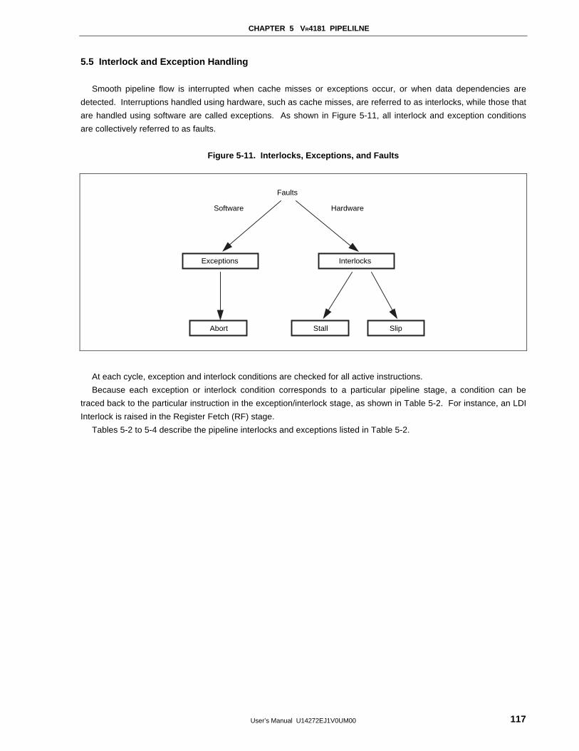
CHAPTER 5 VR4181 PIPELILNE
User’s Manual U14272EJ1V0UM00 117
5.5 Interlock and Exception Handling
Smooth pipeline flow is interrupted when cache misses or exceptions occur, or when data dependencies are
detected. Interruptions handled using hardware, such as cache misses, are referred to as interlocks, while those that
are handled using software are called exceptions. As shown in Figure 5-11, all interlock and exception conditions
are collectively referred to as faults.
Figure 5-11. Interlocks, Exceptions, and Faults
Software Hardware
Faults
Exceptions
Abort Stall Slip
Interlocks
At each cycle, exception and interlock conditions are checked for all active instructions.
Because each exception or interlock condition corresponds to a particular pipeline stage, a condition can be
traced back to the particular instruction in the exception/interlock stage, as shown in Table 5-2. For instance, an LDI
Interlock is raised in the Register Fetch (RF) stage.
Tables 5-2 to 5-4 describe the pipeline interlocks and exceptions listed in Table 5-2.
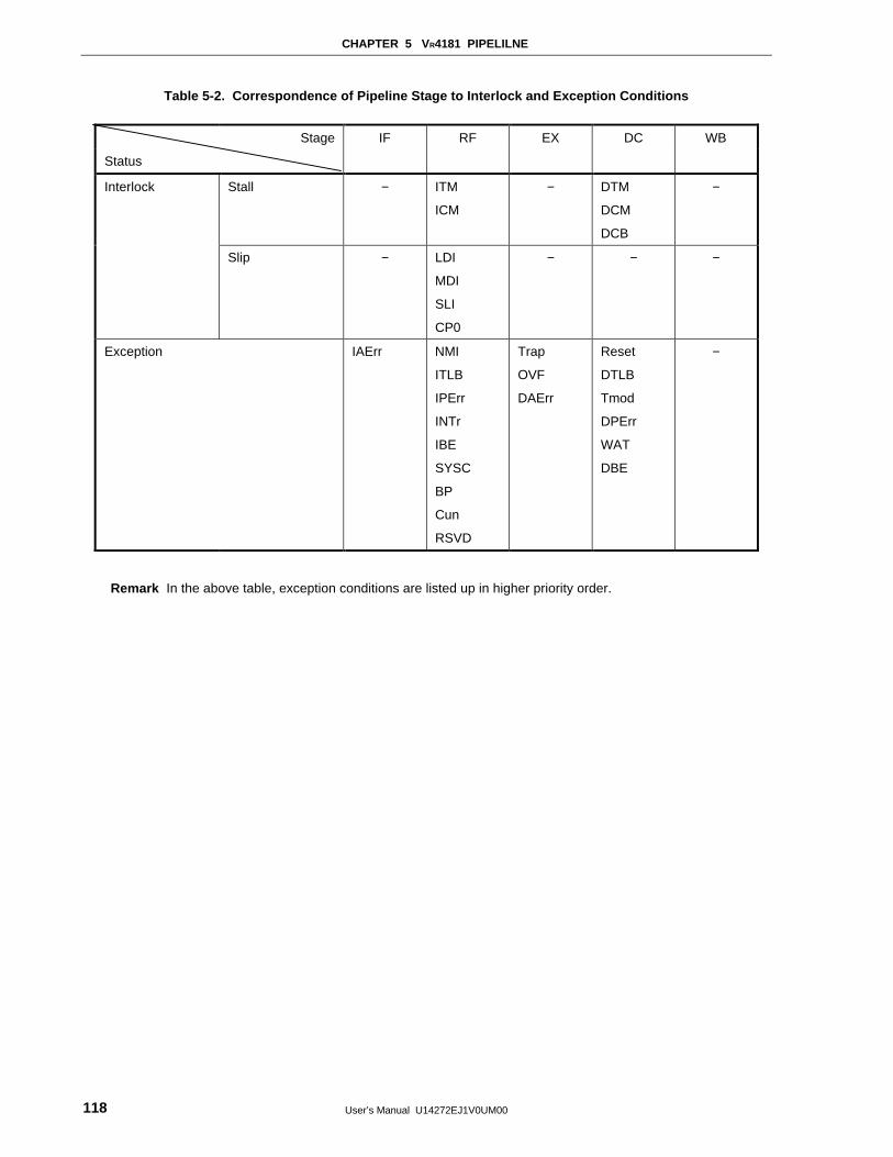
CHAPTER 5 VR4181 PIPELILNE
User’s Manual U14272EJ1V0UM00118
Table 5-2. Correspondence of Pipeline Stage to Interlock and Exception Conditions
Stage IF RF EX DC WB
Status
Interlock Stall − ITM
ICM
− DTM
DCM
DCB
−
Slip − LDI
MDI
SLI
CP0
− − −
Exception IAErr NMI
ITLB
IPErr
INTr
IBE
SYSC
BP
Cun
RSVD
Trap
OVF
DAErr
Reset
DTLB
Tmod
DPErr
WAT
DBE
−
Remark In the above table, exception conditions are listed up in higher priority order.
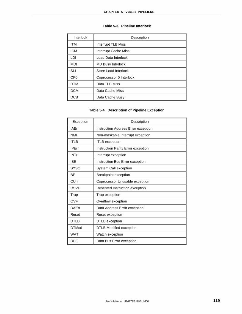
CHAPTER 5 VR4181 PIPELILNE
User’s Manual U14272EJ1V0UM00 119
Table 5-3. Pipeline Interlock
Interlock Description
ITM Interrupt TLB Miss
ICM Interrupt Cache Miss
LDI Load Data Interlock
MDI MD Busy Interlock
SLI Store-Load Interlock
CP0 Coprocessor 0 Interlock
DTM Data TLB Miss
DCM Data Cache Miss
DCB Data Cache Busy
Table 5-4. Description of Pipeline Exception
Exception Description
IAErr Instruction Address Error exception
NMI Non-maskable Interrupt exception
ITLB ITLB exception
IPErr Instruction Parity Error exception
INTr Interrupt exception
IBE Instruction Bus Error exception
SYSC System Call exception
BP Breakpoint exception
CUn Coprocessor Unusable exception
RSVD Reserved Instruction exception
Trap Trap exception
OVF Overflow exception
DAErr Data Address Error exception
Reset Reset exception
DTLB DTLB exception
DTMod DTLB Modified exception
WAT Watch exception
DBE Data Bus Error exception
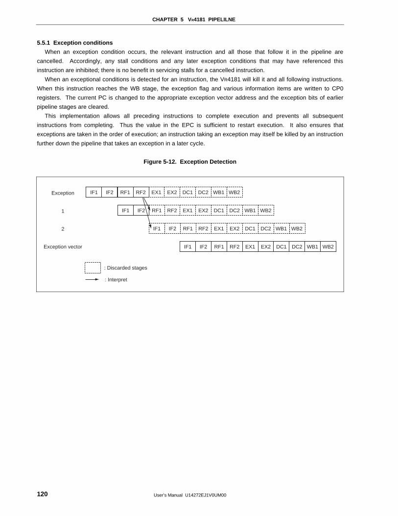
CHAPTER 5 VR4181 PIPELILNE
User’s Manual U14272EJ1V0UM00120
5.5.1 Exception conditions
When an exception condition occurs, the relevant instruction and all those that follow it in the pipeline are
cancelled. Accordingly, any stall conditions and any later exception conditions that may have referenced this
instruction are inhibited; there is no benefit in servicing stalls for a cancelled instruction.
When an exceptional conditions is detected for an instruction, the VR4181 will kill it and all following instructions.
When this instruction reaches the WB stage, the exception flag and various information items are written to CP0
registers. The current PC is changed to the appropriate exception vector address and the exception bits of earlier
pipeline stages are cleared.
This implementation allows all preceding instructions to complete execution and prevents all subsequent
instructions from completing. Thus the value in the EPC is sufficient to restart execution. It also ensures that
exceptions are taken in the order of execution; an instruction taking an exception may itself be killed by an instruction
further down the pipeline that takes an exception in a later cycle.
Figure 5-12. Exception Detection
: Discarded stages
: Interpret
Exception
1
2
Exception vector
RF1 EX1 DC1 WB1IF1 EX2 DC2 WB2IF2
RF1 EX1 DC1 WB1IF1 RF2 EX2 DC2 WB2IF2
RF1 EX1 DC1 WB1IF1 RF2 EX2 DC2 WB2IF2
RF1 EX1 DC1 WB1IF1 RF2 EX2 DC2 WB2IF2
RF2
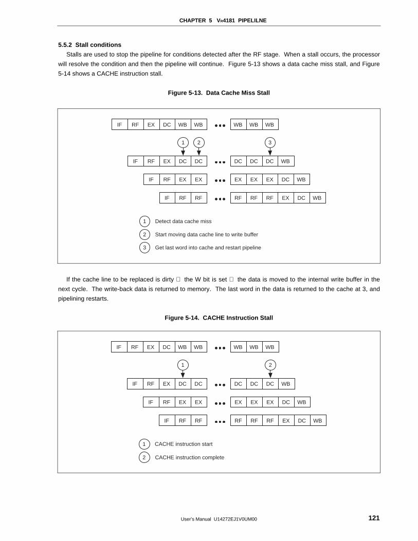
CHAPTER 5 VR4181 PIPELILNE
User’s Manual U14272EJ1V0UM00 121
5.5.2 Stall conditions
Stalls are used to stop the pipeline for conditions detected after the RF stage. When a stall occurs, the processor
will resolve the condition and then the pipeline will continue. Figure 5-13 shows a data cache miss stall, and Figure
5-14 shows a CACHE instruction stall.
Figure 5-13. Data Cache Miss Stall
1
IF RF EX DC WB WB WB WB WB
IF RF EX DC DC DC DC DC WB
IF RF EX EX EX EX EX DC WB
IF RF RF RF RF RF EX DC WB
2 3
1
2
3
Detect data cache miss
Start moving data cache line to write buffer
Get last word into cache and restart pipeline
If the cache line to be replaced is dirty the W bit is set the data is moved to the internal write buffer in the
next cycle. The write-back data is returned to memory. The last word in the data is returned to the cache at 3, and
pipelining restarts.
Figure 5-14. CACHE Instruction Stall
1
IF RF EX DC WB WB WB WB WB
IF RF EX DC DC DC DC DC WB
IF RF EX EX EX EX EX DC WB
IF RF RF RF RF RF EX DC WB
2
1
2 CACHE instruction complete
CACHE instruction start
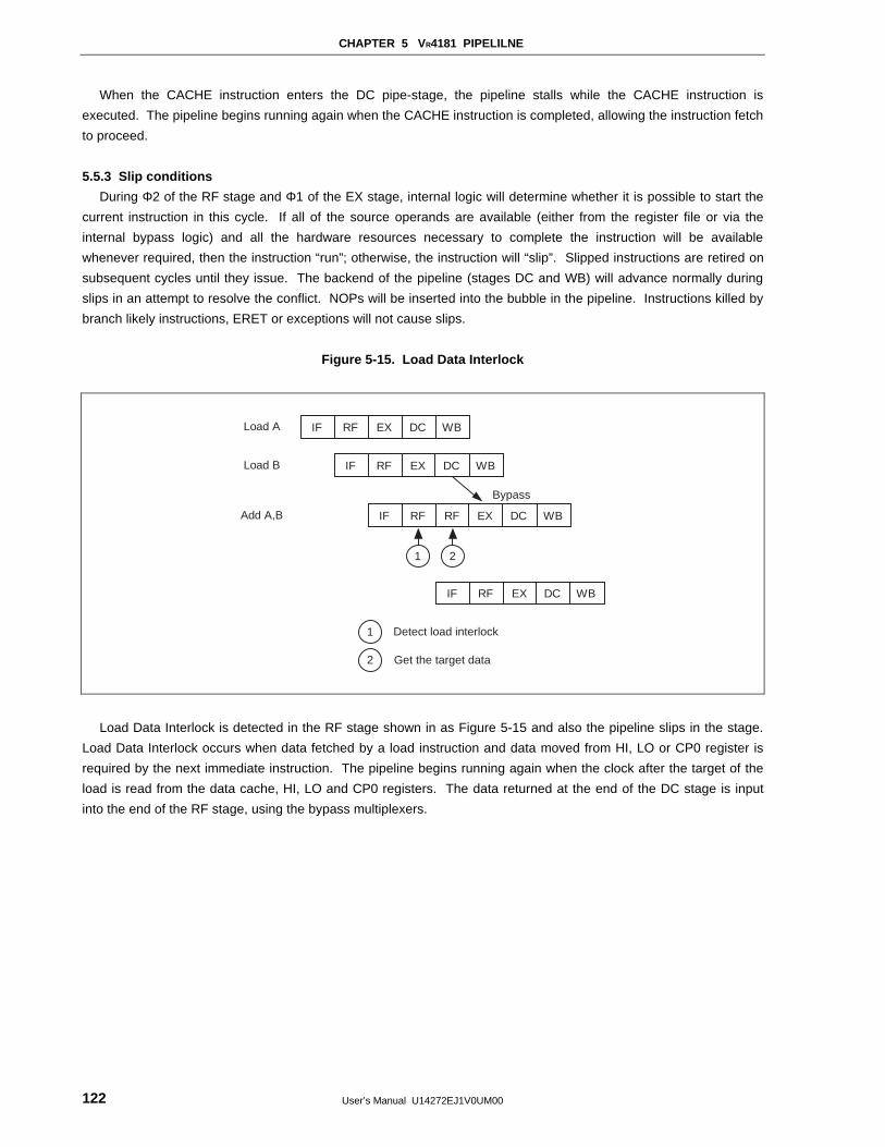
CHAPTER 5 VR4181 PIPELILNE
User’s Manual U14272EJ1V0UM00122
When the CACHE instruction enters the DC pipe-stage, the pipeline stalls while the CACHE instruction is
executed. The pipeline begins running again when the CACHE instruction is completed, allowing the instruction fetch
to proceed.
5.5.3 Slip conditions
During Φ2 of the RF stage and Φ1 of the EX stage, internal logic will determine whether it is possible to start the
current instruction in this cycle. If all of the source operands are available (either from the register file or via the
internal bypass logic) and all the hardware resources necessary to complete the instruction will be available
whenever required, then the instruction “run”; otherwise, the instruction will “slip”. Slipped instructions are retired on
subsequent cycles until they issue. The backend of the pipeline (stages DC and WB) will advance normally during
slips in an attempt to resolve the conflict. NOPs will be inserted into the bubble in the pipeline. Instructions killed by
branch likely instructions, ERET or exceptions will not cause slips.
Figure 5-15. Load Data Interlock
1
Add A,B
Load B
Load A IF RF EX DC
IF RF EX DC
IF RF RF EX DC
RF EX DC WB
1
2
2
WB
WB
IF
WB
Get the target data
Detect load interlock
Bypass
Load Data Interlock is detected in the RF stage shown in as Figure 5-15 and also the pipeline slips in the stage.
Load Data Interlock occurs when data fetched by a load instruction and data moved from HI, LO or CP0 register is
required by the next immediate instruction. The pipeline begins running again when the clock after the target of the
load is read from the data cache, HI, LO and CP0 registers. The data returned at the end of the DC stage is input
into the end of the RF stage, using the bypass multiplexers.
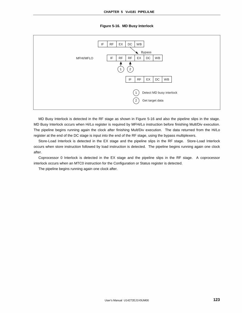
CHAPTER 5 VR4181 PIPELILNE
User’s Manual U14272EJ1V0UM00 123
Figure 5-16. MD Busy Interlock
MFHI/MFLO
IF RF EX DC WB
EX DC WB
1
2
RFIF
Get target data
Detect MD busy interlock
1
IF RF RF EX DC
2
WB
Bypass
MD Busy Interlock is detected in the RF stage as shown in Figure 5-16 and also the pipeline slips in the stage.
MD Busy Interlock occurs when Hi/Lo register is required by MFHi/Lo instruction before finishing Mult/Div execution.
The pipeline begins running again the clock after finishing Mult/Div execution. The data returned from the Hi/Lo
register at the end of the DC stage is input into the end of the RF stage, using the bypass multiplexers.
Store-Load Interlock is detected in the EX stage and the pipeline slips in the RF stage. Store-Load Interlock
occurs when store instruction followed by load instruction is detected. The pipeline begins running again one clock
after.
Coprocessor 0 Interlock is detected in the EX stage and the pipeline slips in the RF stage. A coprocessor
interlock occurs when an MTC0 instruction for the Configuration or Status register is detected.
The pipeline begins running again one clock after.
CHAPTER 5 VR4181 PIPELILNE
User’s Manual U14272EJ1V0UM00124
5.5.4 Bypassing
In some cases, data and conditions produced in the EX, DC and WB stages of the pipeline are made available to
the EX stage (only) through the bypass data path.
Operand bypass allows an instruction in the EX stage to continue without having to wait for data or conditions to
be written to the register file at the end of the WB stage. Instead, the Bypass Control Unit is responsible for ensuring
data and conditions from later pipeline stages are available at the appropriate time for instructions earlier in the
pipeline.
The Bypass Control Unit is also responsible for controlling the source and destination register addresses supplied
to the register file.
5.6 Code Compatibility
The VR4110 CPU core can execute all programs that can be executed in other VR-Series processors. But the
reverse is not necessarily true. Programs complied using a standard MIPS compiler can be executed in both types of
processors. When using manual assembly, however, write programs carefully so that compatibility with other VR-
series processors can be maintained. Matters which should be paid attention to when porting programs between the
VR4110 CPU core and other VR-Series processors are listed below.
• The VR4110 CPU core does not support floating-point instructions since it has no Floating-Point Unit (FPU).
• Multiply-add instructions (DMADD16, MADD16) are added in the VR4110 CPU core.
• Instructions for power modes (HIBERNATE, STANDBY, SUSPEND) are added in the VR4110 CPU core to
support power modes.
• The VR4110 CPU core does not have the LL bit to perform synchronization of multiprocessing. Therefore, the
CPU core does not support instructions which manipulate the LL bit (LL, LLD, SC, SCD).
• A 16-bit length MIPS16 instruction set is added in the VR4110 CPU core.
• The CP0 hazards of the VR4110 CPU core are equally or less stringent than those of other processors (see
Chapter 29 for details).
For more information, refer to Chapters 3, 4, 27, and 28, VR4100 User’s Manual , or VR4300TM, VR4305TM,
VR4310TM User’s Manual .
User’s Manual U14272EJ1V0UM00 125
CHAPTER 6 MEMORY MANAGEMENT SYSTEM
The VR4181 provides a memory management unit (MMU) which uses a translation lookaside buffer (TLB) to
translate virtual addresses into physical addresses. This chapter describes the virtual and physical address spaces,
the virtual-to-physical address translation, the operation of the TLB in making these translations, and the CP0
registers that provide the software interface to the TLB.
6.1 Translation Lookaside Buffer (TLB)
Virtual addresses are translated into physical addresses using an on-chip TLB. The on-chip TLB is a fully-
associative memory that holds 32 entries, which provide mapping to 32 odd/even page pairs for one entry. The
pages can have five different sizes, 1 K, 4 K, 16 K, 64 K, and 256 K, and can be specified in each entry. If it is
supplied with a virtual address, each of the 32 TLB entries is checked simultaneously to see whether they match the
virtual addresses that are provided with the ASID field and saved in the EntryHi register.
If there is a virtual address match, or “hit,” in the TLB, the physical page number is extracted from the TLB and
concatenated with the offset to form the physical address.
If no match occurs (TLB “miss”), an exception is taken and software refills the TLB from the page table resident in
memory. The software writes to an entry selected using the Index register or a random entry indicated in the
Random register.
If more than one entry in the TLB matches the virtual address being translated, the operation is undefined and the
TLB may be disabled. In this case, the TLB-Shutdown (TS) bit of the Status register is set to 1, and the TLB
becomes unusable (an attempt to access the TLB results in a TLB Mismatch exception regardless of whether there is
an entry that hits). The TS bit can be cleared only by a reset.
Note that virtual addresses may be converted to physical addresses without using a TLB, depending on the
address space that is being subjected to address translation. For example, address translation for the kseg0 or
kseg1 address space does not use mapping. The physical addresses of these address spaces are determined by
subtracting the base address of the address space from the virtual addresses.
6.2 Virtual Address Space
The address space of the CPU is extended in memory management system, by converting (translating) huge
virtual memory addresses into physical addresses.
The physical address space of the VR4181 is 4 Gbytes and 32-bit width addresses are used.
For the virtual address space, up to 2 Gbytes (231) are provided as a user’s area and 32-bit width addresses are
used in the 32-bit mode. In the 64-bit mode, up to 1 Tbyte (240) is provided as a user’s area and 64-bit width
addresses are used. For the format of the TLB entry in each mode, refer to 6.4.1.
As shown in Figures 6-2 and 6-3, the virtual address is extended with an address space identifier (ASID), which
reduces the frequency of TLB flushing when switching contexts. This 8-bit ASID is in the CP0 EntryHi register, and
the Global (G) bit is in the EntryLo0 and EntryLo1 registers, described later in this chapter.
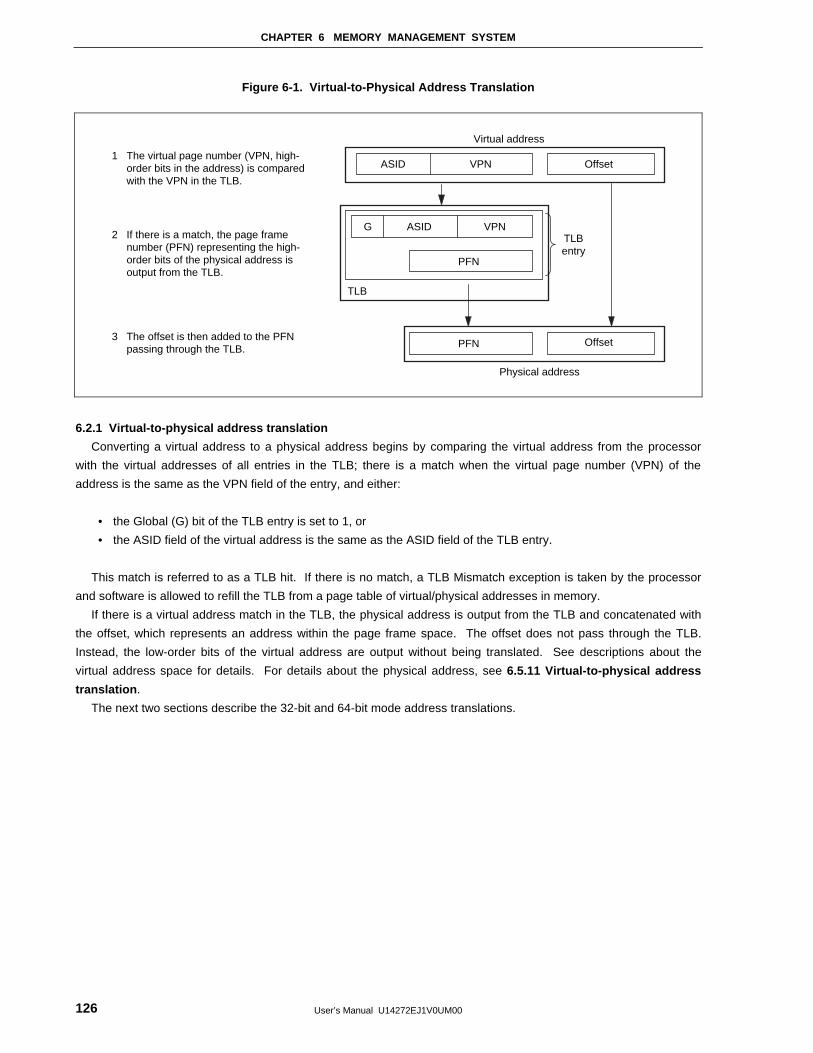
CHAPTER 6 MEMORY MANAGEMENT SYSTEM
User’s Manual U14272EJ1V0UM00126
Figure 6-1. Virtual-to-Physical Address Translation
ASID VPN
G
1 The virtual page number (VPN, high- order bits in the address) is compared with the VPN in the TLB.
2 If there is a match, the page frame number (PFN) representing the high- order bits of the physical address is output from the TLB.
3 The offset is then added to the PFN passing through the TLB.
ASID
PFN
PFN
Physical address
TLB
VPNTLBentry
Virtual address
Offset
Offset
6.2.1 Virtual-to-physical address translation
Converting a virtual address to a physical address begins by comparing the virtual address from the processor
with the virtual addresses of all entries in the TLB; there is a match when the virtual page number (VPN) of the
address is the same as the VPN field of the entry, and either:
• the Global (G) bit of the TLB entry is set to 1, or
• the ASID field of the virtual address is the same as the ASID field of the TLB entry.
This match is referred to as a TLB hit. If there is no match, a TLB Mismatch exception is taken by the processor
and software is allowed to refill the TLB from a page table of virtual/physical addresses in memory.
If there is a virtual address match in the TLB, the physical address is output from the TLB and concatenated with
the offset, which represents an address within the page frame space. The offset does not pass through the TLB.
Instead, the low-order bits of the virtual address are output without being translated. See descriptions about the
virtual address space for details. For details about the physical address, see 6.5.11 Virtual-to-physical address
translation .
The next two sections describe the 32-bit and 64-bit mode address translations.
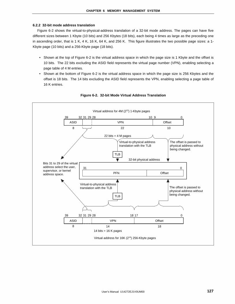
CHAPTER 6 MEMORY MANAGEMENT SYSTEM
User’s Manual U14272EJ1V0UM00 127
6.2.2 32-bit mode address translation
Figure 6-2 shows the virtual-to-physical-address translation of a 32-bit mode address. The pages can have five
different sizes between 1 Kbyte (10 bits) and 256 Kbytes (18 bits), each being 4 times as large as the preceding one
in ascending order, that is 1 K, 4 K, 16 K, 64 K, and 256 K. This figure illustrates the two possible page sizes: a 1-
Kbyte page (10 bits) and a 256-Kbyte page (18 bits).
• Shown at the top of Figure 6-2 is the virtual address space in which the page size is 1 Kbyte and the offset is
10 bits. The 22 bits excluding the ASID field represents the virtual page number (VPN), enabling selecting a
page table of 4 M entries.
• Shown at the bottom of Figure 6-2 is the virtual address space in which the page size is 256 Kbytes and the
offset is 18 bits. The 14 bits excluding the ASID field represents the VPN, enabling selecting a page table of
16 K entries.
Figure 6-2. 32-bit Mode Virtual Address Translation
39
8 22
TLB
TLB
22 bits = 4 M pages
Virtual-to-physical addresstranslation with the TLB
Bits 31 to 29 of the virtualaddress select the user,supervisor, or kerneladdress space.
The offset is passed tophysical address withoutbeing changed.
The offset is passed tophysical address withoutbeing changed.
Virtual address for 4M (222) 1-Kbyte pages
32-bit physical address
14 bits = 16 K pages
PFN Offset
10
ASID VPN Offset
32 31
31 0
29 28 10 9 0
39
8 14 18
ASID VPN Offset
32 31 29 28 18 17 0
Virtual-to-physical addresstranslation with the TLB
Virtual address for 16K (214) 256-Kbyte pages
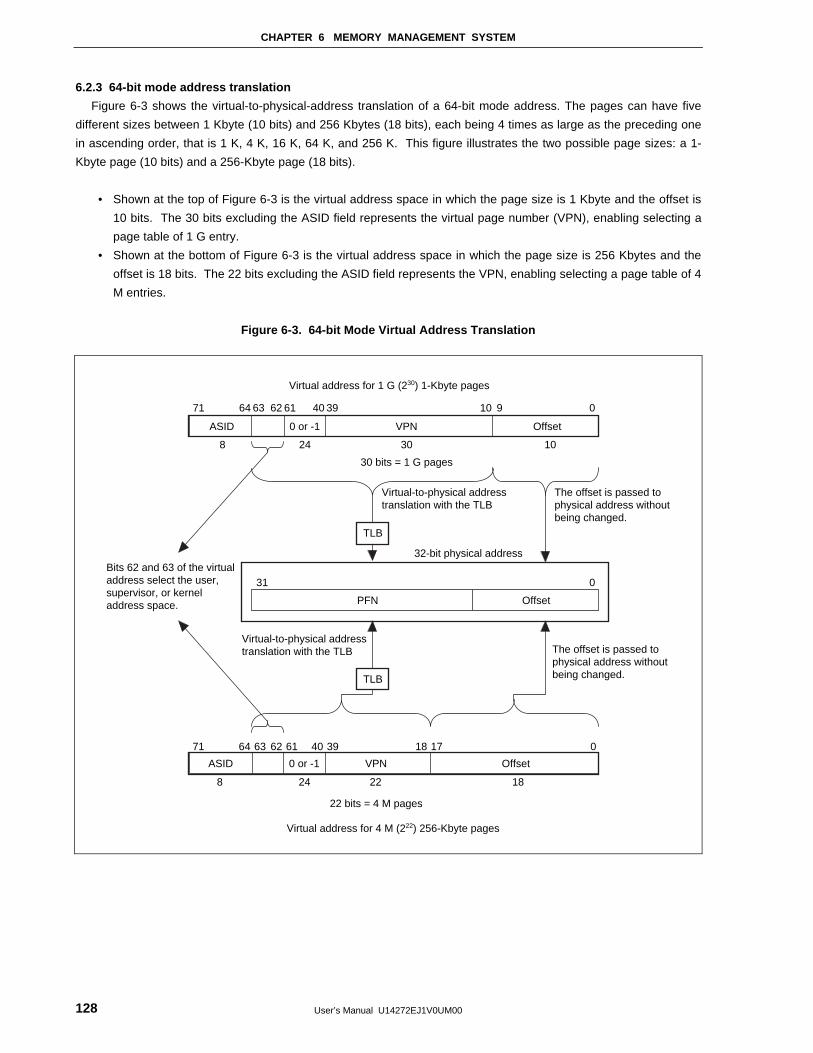
CHAPTER 6 MEMORY MANAGEMENT SYSTEM
User’s Manual U14272EJ1V0UM00128
6.2.3 64-bit mode address translation
Figure 6-3 shows the virtual-to-physical-address translation of a 64-bit mode address. The pages can have five
different sizes between 1 Kbyte (10 bits) and 256 Kbytes (18 bits), each being 4 times as large as the preceding one
in ascending order, that is 1 K, 4 K, 16 K, 64 K, and 256 K. This figure illustrates the two possible page sizes: a 1-
Kbyte page (10 bits) and a 256-Kbyte page (18 bits).
• Shown at the top of Figure 6-3 is the virtual address space in which the page size is 1 Kbyte and the offset is
10 bits. The 30 bits excluding the ASID field represents the virtual page number (VPN), enabling selecting a
page table of 1 G entry.
• Shown at the bottom of Figure 6-3 is the virtual address space in which the page size is 256 Kbytes and the
offset is 18 bits. The 22 bits excluding the ASID field represents the VPN, enabling selecting a page table of 4
M entries.
Figure 6-3. 64-bit Mode Virtual Address Translation
71 64 63 62 61 40 39 10 9 0
8 24 30 10
TLB
TLB
PFN Offset
ASID 0 or -1 VPN Offset
31 0
71
8 2224 18
ASID 0 or -1 VPN Offset
64 63 62 61 18 1740 39 0
30 bits = 1 G pages
Virtual-to-physical addresstranslation with the TLB
Bits 62 and 63 of the virtualaddress select the user,supervisor, or kerneladdress space.
The offset is passed tophysical address withoutbeing changed.
The offset is passed tophysical address withoutbeing changed.
Virtual address for 1 G (230) 1-Kbyte pages
32-bit physical address
22 bits = 4 M pages
Virtual-to-physical addresstranslation with the TLB
Virtual address for 4 M (222) 256-Kbyte pages
CHAPTER 6 MEMORY MANAGEMENT SYSTEM
User’s Manual U14272EJ1V0UM00 129
6.2.4 Operating modes
The processor has three operating modes that function in both 32- and 64-bit operations:
• User mode
• Supervisor mode
• Kernel mode
User and Kernel modes are common to all VR-Series processors. Generally, Kernel mode is used to executing the
operating system, while User mode is used to run application programs. The VR4000 series processors have a third
mode, which is called Supervisor mode and categorized in between User and Kernel modes. This mode is used to
configure a high-security system.
When an exception occurs, the CPU enters Kernel mode, and remains in this mode until an exception return
instruction (ERET) is executed. The ERET instruction brings back the processor to the mode in which it was just
before the exception occurs.
These modes are described in the next three sections.
6.2.5 User mode virtual addressing
During User mode, a 2-Gbyte (231 bytes) virtual address space (useg) can be used in the 32-bit mode. In the 64-bit
mode, a 1-Tbyte (240 bytes) virtual address space (xuseg) can be used.
As shown in Tables 6-2 and 6-3, each virtual address is extended independently as another virtual address by
setting an 8-bit address space ID area (ASID), to support user processes of up to 256. The contents of TLB can be
retained after context switching by allocating each process by ASID. useg and xuseg can be referenced via TLB.
Whether a cache is used or not is determined for each page by the TLB entry (depending on the C bit setting in the
TLB entry).
The User segment starts at address 0 and the current active user process resides in either useg (in 32-bit mode)
or xuseg (in 64-bit mode). The TLB identically maps all references to useg/xuseg from all modes, and controls cache
accessibility.
The processor operates in User mode when the Status register contains the following bit-values:
• KSU = 10
• EXL = 0
• ERL = 0
In conjunction with these bits, the UX bit in the Status register selects 32- or 64-bit User mode addressing as
follows:
• When UX = 0, 32-bit useg space is selected.
• When UX = 1, 64-bit xuseg space is selected.
Table 6-1 lists the characteristics of each user segment (useg and xuseg).
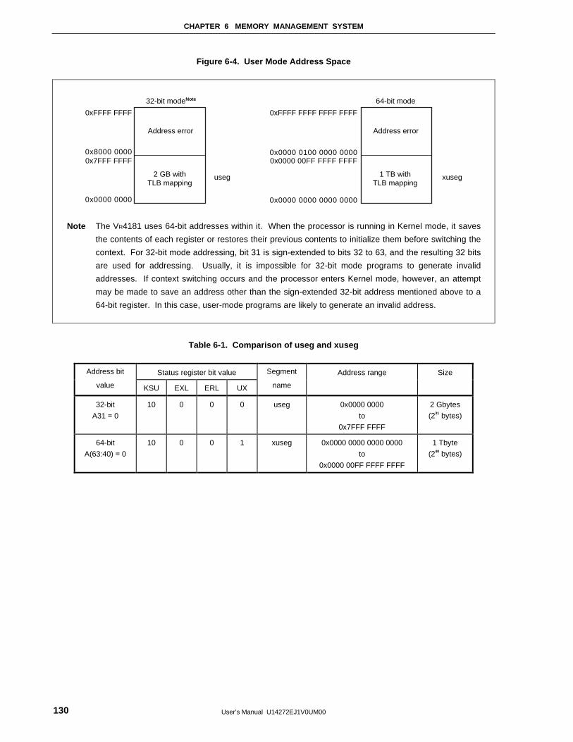
CHAPTER 6 MEMORY MANAGEMENT SYSTEM
User’s Manual U14272EJ1V0UM00130
Figure 6-4. User Mode Address Space
0xFFFF FFFF
0x8000 00000x7FFF FFFF
0x0000 0000
0xFFFF FFFF FFFF FFFF
0x0000 0100 0000 00000x0000 00FF FFFF FFFF
0x0000 0000 0000 0000
useg xuseg
64-bit mode32-bit modeNote
Address error
2 GB withTLB mapping
Address error
1 TB withTLB mapping
Note The VR4181 uses 64-bit addresses within it. When the processor is running in Kernel mode, it saves
the contents of each register or restores their previous contents to initialize them before switching the
context. For 32-bit mode addressing, bit 31 is sign-extended to bits 32 to 63, and the resulting 32 bits
are used for addressing. Usually, it is impossible for 32-bit mode programs to generate invalid
addresses. If context switching occurs and the processor enters Kernel mode, however, an attempt
may be made to save an address other than the sign-extended 32-bit address mentioned above to a
64-bit register. In this case, user-mode programs are likely to generate an invalid address.
Table 6-1. Comparison of useg and xuseg
Address bit Status register bit value Segment Address range Size
value KSU EXL ERL UX name
32-bit
A31 = 0
10 0 0 0 useg 0x0000 0000
to
0x7FFF FFFF
2 Gbytes
(231 bytes)
64-bit
A(63:40) = 0
10 0 0 1 xuseg 0x0000 0000 0000 0000
to
0x0000 00FF FFFF FFFF
1 Tbyte
(240 bytes)
CHAPTER 6 MEMORY MANAGEMENT SYSTEM
User’s Manual U14272EJ1V0UM00 131
(1) useg (32-bit mode)
In User mode, when UX = 0 in the Status register and the most significant bit of the virtual address is 0, this
virtual address space is labeled useg.
Any attempt to reference an address with the most-significant bit set while in User mode causes an Address
Error exception (see CHAPTER 7 EXCEPTION PROCESSING).
The TLB Refill exception vector is used for TLB misses.
(2) xuseg (64-bit mode)
In User mode, when UX = 1 in the Status register and bits 63 to 40 of the virtual address are all 0, this virtual
address space is labeled xuseg.
Any attempt to reference an address with bits 63:40 equal to 1 causes an Address Error exception (see
CHAPTER 7 EXCEPTION PROCESSING).
The XTLB Refill exception vector is used for TLB misses.
6.2.6 Supervisor mode virtual addressing
Supervisor mode shown in Figure 6-5 is designed for layered operating systems in which a true kernel runs in
Kernel mode, and the rest of the operating system runs in Supervisor mode.
All of the suseg, sseg, xsuseg, xsseg, and csseg spaces are referenced via TLB. Whether cache can be used or
not is determined by bit C of each page’s TLB entry.
The processor operates in Supervisor mode when the Status register contains the following bit-values:
• KSU = 01
• EXL = 0
• ERL = 0
In conjunction with these bits, the SX bit in the Status register selects 32- or 64-bit Supervisor mode addressing:
• When SX = 0, 32-bit supervisor space is selected.
• When SX = 1, 64-bit supervisor space is selected.
Figure 6-5 shows the supervisor mode address space, and Table 6-2 lists the characteristics of the Supervisor
mode segments.
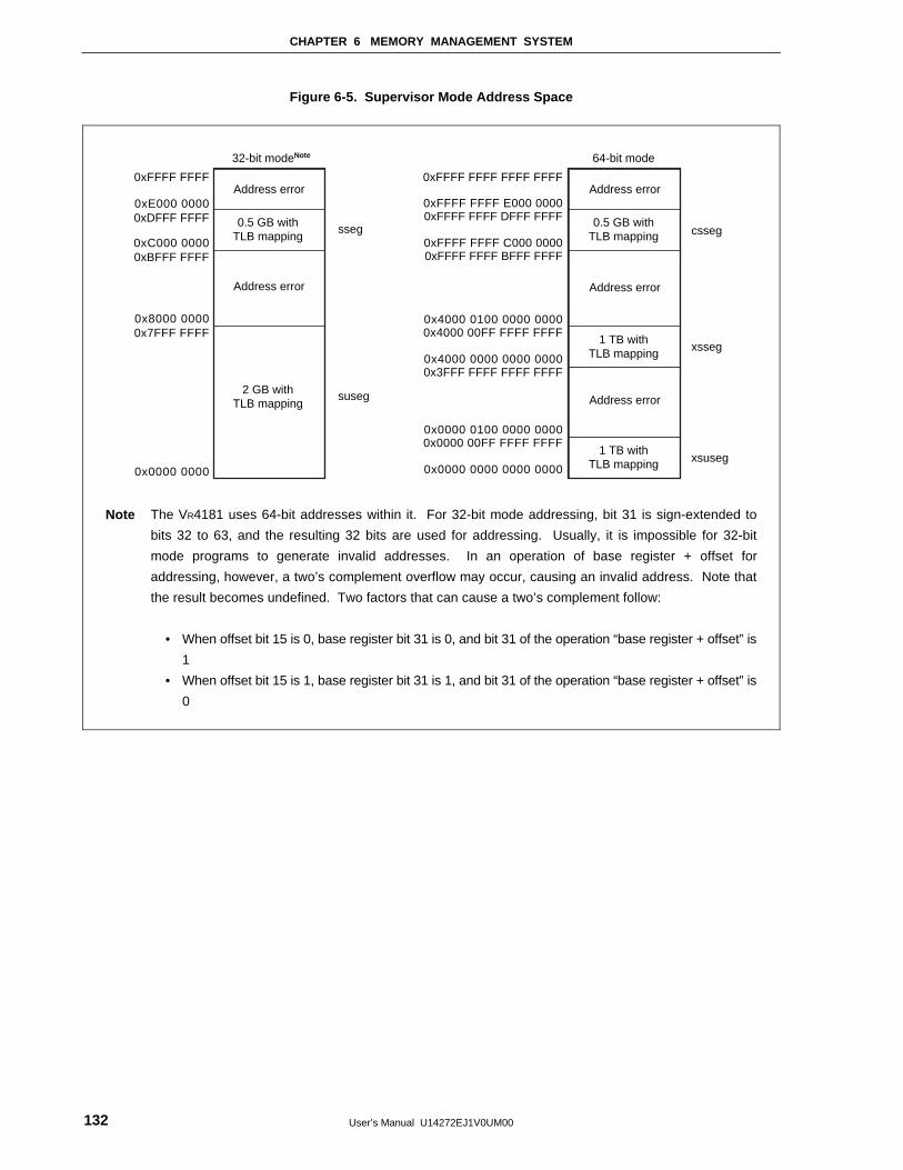
CHAPTER 6 MEMORY MANAGEMENT SYSTEM
User’s Manual U14272EJ1V0UM00132
Figure 6-5. Supervisor Mode Address Space
0xFFFF FFFF
0xC000 00000xBFFF FFFF
0x8000 00000x7FFF FFFF
0x0000 0000
0xE000 00000xDFFF FFFF
0xFFFF FFFF FFFF FFFF
0xFFFF FFFF C000 00000xFFFF FFFF BFFF FFFF
0xFFFF FFFF E000 00000xFFFF FFFF DFFF FFFF
0x4000 0000 0000 00000x3FFF FFFF FFFF FFFF
0x4000 0100 0000 00000x4000 00FF FFFF FFFF
0x0000 0000 0000 0000
0x0000 0100 0000 00000x0000 00FF FFFF FFFF
suseg
sseg csseg
xsseg
xsuseg
64-bit mode32-bit modeNote
Address error
Address error
0.5 GB withTLB mapping
2 GB withTLB mapping
Address error
Address error
Address error
0.5 GB withTLB mapping
1 TB withTLB mapping
1 TB withTLB mapping
Note The VR4181 uses 64-bit addresses within it. For 32-bit mode addressing, bit 31 is sign-extended to
bits 32 to 63, and the resulting 32 bits are used for addressing. Usually, it is impossible for 32-bit
mode programs to generate invalid addresses. In an operation of base register + offset for
addressing, however, a two’s complement overflow may occur, causing an invalid address. Note that
the result becomes undefined. Two factors that can cause a two’s complement follow:
• When offset bit 15 is 0, base register bit 31 is 0, and bit 31 of the operation “base register + offset” is
1
• When offset bit 15 is 1, base register bit 31 is 1, and bit 31 of the operation “base register + offset” is
0
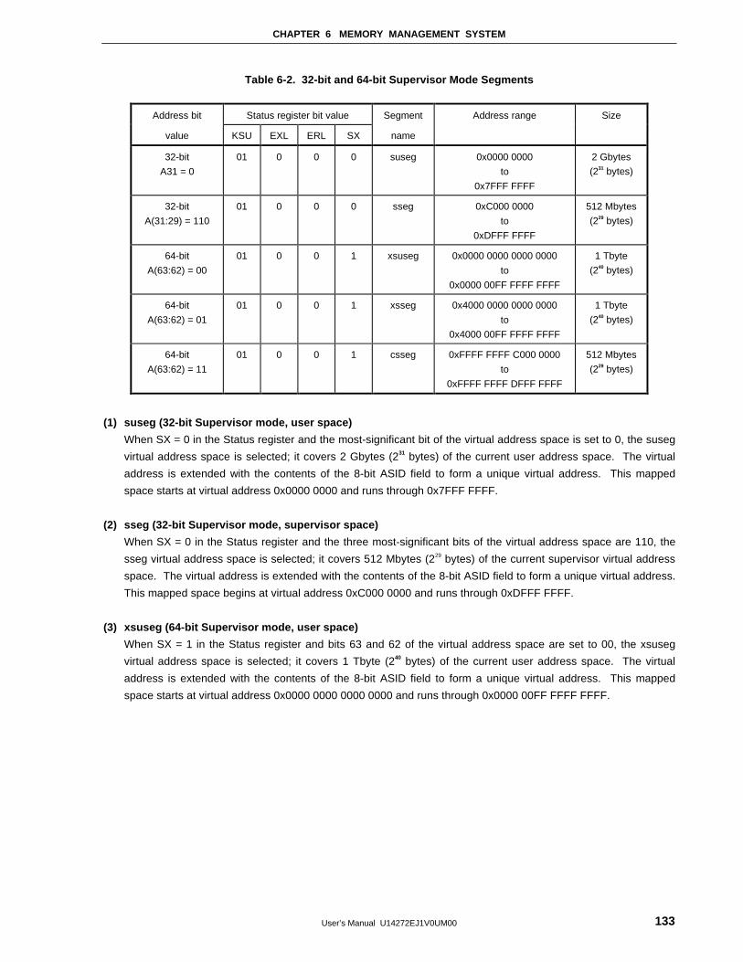
CHAPTER 6 MEMORY MANAGEMENT SYSTEM
User’s Manual U14272EJ1V0UM00 133
Table 6-2. 32-bit and 64-bit Supervisor Mode Segments
Address bit Status register bit value Segment Address range Size
value KSU EXL ERL SX name
32-bit
A31 = 0
01 0 0 0 suseg 0x0000 0000
to
0x7FFF FFFF
2 Gbytes
(231 bytes)
32-bit
A(31:29) = 110
01 0 0 0 sseg 0xC000 0000
to
0xDFFF FFFF
512 Mbytes
(229 bytes)
64-bit
A(63:62) = 00
01 0 0 1 xsuseg 0x0000 0000 0000 0000
to
0x0000 00FF FFFF FFFF
1 Tbyte
(240 bytes)
64-bit
A(63:62) = 01
01 0 0 1 xsseg 0x4000 0000 0000 0000
to
0x4000 00FF FFFF FFFF
1 Tbyte
(240 bytes)
64-bit
A(63:62) = 11
01 0 0 1 csseg 0xFFFF FFFF C000 0000
to
0xFFFF FFFF DFFF FFFF
512 Mbytes
(229 bytes)
(1) suseg (32-bit Supervisor mode, user space)
When SX = 0 in the Status register and the most-significant bit of the virtual address space is set to 0, the suseg
virtual address space is selected; it covers 2 Gbytes (231 bytes) of the current user address space. The virtual
address is extended with the contents of the 8-bit ASID field to form a unique virtual address. This mapped
space starts at virtual address 0x0000 0000 and runs through 0x7FFF FFFF.
(2) sseg (32-bit Supervisor mode, supervisor space)
When SX = 0 in the Status register and the three most-significant bits of the virtual address space are 110, the
sseg virtual address space is selected; it covers 512 Mbytes (229 bytes) of the current supervisor virtual address
space. The virtual address is extended with the contents of the 8-bit ASID field to form a unique virtual address.
This mapped space begins at virtual address 0xC000 0000 and runs through 0xDFFF FFFF.
(3) xsuseg (64-bit Supervisor mode, user space)
When SX = 1 in the Status register and bits 63 and 62 of the virtual address space are set to 00, the xsuseg
virtual address space is selected; it covers 1 Tbyte (240 bytes) of the current user address space. The virtual
address is extended with the contents of the 8-bit ASID field to form a unique virtual address. This mapped
space starts at virtual address 0x0000 0000 0000 0000 and runs through 0x0000 00FF FFFF FFFF.
CHAPTER 6 MEMORY MANAGEMENT SYSTEM
User’s Manual U14272EJ1V0UM00134
(4) xsseg (64-bit Supervisor mode, current supervisor space)
When SX = 1 in the Status register and bits 63 and 62 of the virtual address space are set to 01, the xsseg
virtual address space is selected; it covers 1 Tbyte (240 bytes) of the current supervisor virtual address space.
The virtual address is extended with the contents of the 8-bit ASID field to form a unique virtual address. This
mapped space begins at virtual address 0x4000 0000 0000 0000 and runs through 0x4000 00FF FFFF FFFF.
(5) csseg (64-bit Supervisor mode, separate supervisor space)
When SX = 1 in the Status register and bits 63 and 62 of the virtual address space are set to 11, the csseg
virtual address space is selected; it covers 512 Mbytes (229 bytes) of the separate supervisor virtual address
space. The virtual address is extended with the contents of the 8-bit ASID field to form a unique virtual address.
This mapped space begins at virtual address 0xFFFF FFFF C000 0000 and runs through 0xFFFF FFFF DFFF
FFFF.
6.2.7 Kernel mode virtual addressing
If the Status register satisfies any of the following conditions, the processor runs in Kernel mode.
• KSU = 00
• EXL = 1
• ERL = 1
The addressing width in Kernel mode varies according to the state of the KX bit of the Status register, as follows:
• When KX = 0, 32-bit kernel space is selected.
• When KX = 1, 64-bit kernel space is selected.
The processor enters Kernel mode whenever an exception is detected and it remains in Kernel mode until an
exception return (ERET) instruction is executed and results in ERL and/or EXL = 0. The ERET instruction restores
the processor to the mode existing prior to the exception.
Kernel mode virtual address space is divided into regions differentiated by the high-order bits of the virtual
address, as shown in Figure 6-6. Table 6-3 lists the characteristics of the 32-bit Kernel mode segments, and Table
6-4 lists the characteristics of the 64-bit Kernel mode segments.
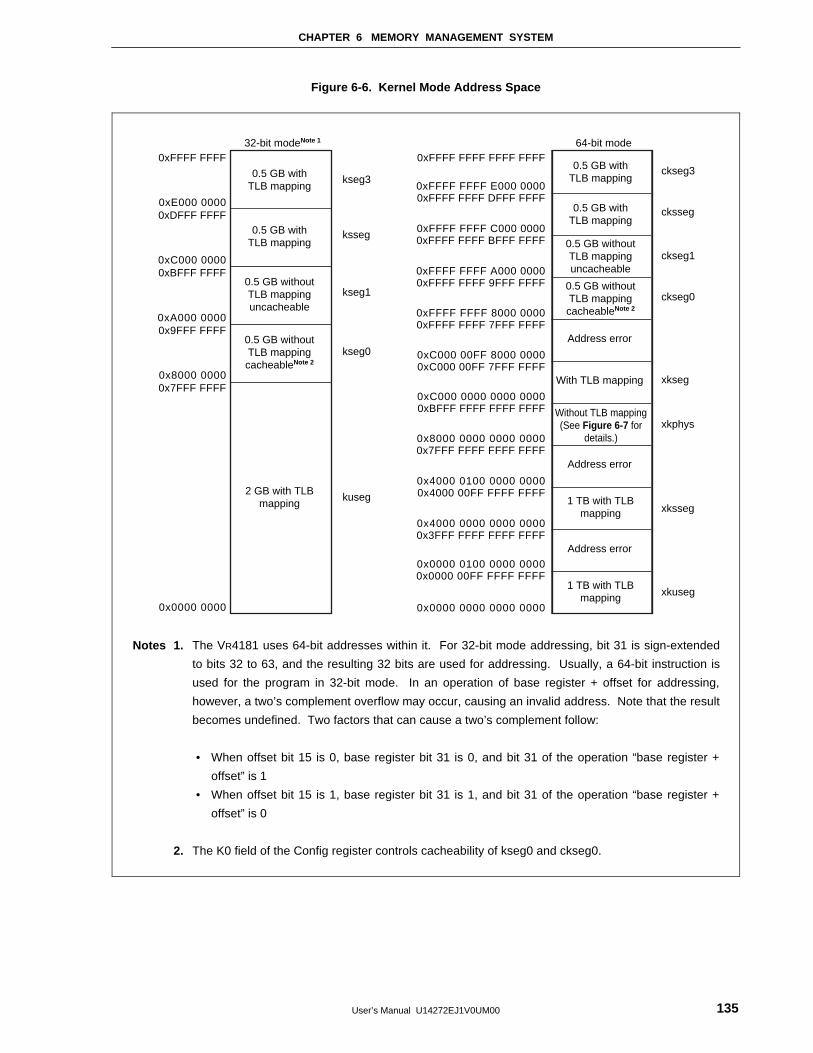
CHAPTER 6 MEMORY MANAGEMENT SYSTEM
User’s Manual U14272EJ1V0UM00 135
Figure 6-6. Kernel Mode Address Space
0xFFFF FFFF
0xC000 00000xBFFF FFFF
0xA000 00000x9FFF FFFF
0x8000 00000x7FFF FFFF
0x0000 0000
0xE000 00000xDFFF FFFF
0xFFFF FFFF FFFF FFFF
0xFFFF FFFF A000 00000xFFFF FFFF 9FFF FFFF
0xFFFF FFFF E000 00000xFFFF FFFF DFFF FFFF
0xFFFF FFFF C000 00000xFFFF FFFF BFFF FFFF
0xC000 00FF 8000 00000xC000 00FF 7FFF FFFF
0xFFFF FFFF 8000 00000xFFFF FFFF 7FFF FFFF
0x0000 0000 0000 0000
0xC000 0000 0000 00000xBFFF FFFF FFFF FFFF
0x8000 0000 0000 00000x7FFF FFFF FFFF FFFF
0x4000 0100 0000 00000x4000 00FF FFFF FFFF
0x4000 0000 0000 00000x3FFF FFFF FFFF FFFF
0x0000 0100 0000 00000x0000 00FF FFFF FFFF
kuseg
kseg3
ksseg
kseg1
kseg0
ckseg3
cksseg
ckseg1
ckseg0
xkseg
xkphys
xksseg
xkuseg
32-bit modeNote 1
Address error
Address error
Address error
With TLB mapping
Without TLB mapping(See Figure 6-7 for
details.)
0.5 GB withTLB mapping
0.5 GB withTLB mapping
0.5 GB withoutTLB mappinguncacheable
0.5 GB withoutTLB mappingcacheableNote 2
2 GB with TLBmapping
64-bit mode
0.5 GB withTLB mapping
0.5 GB withTLB mapping
0.5 GB withoutTLB mappinguncacheable
0.5 GB withoutTLB mappingcacheableNote 2
1 TB with TLBmapping
1 TB with TLBmapping
Notes 1. The VR4181 uses 64-bit addresses within it. For 32-bit mode addressing, bit 31 is sign-extended
to bits 32 to 63, and the resulting 32 bits are used for addressing. Usually, a 64-bit instruction is
used for the program in 32-bit mode. In an operation of base register + offset for addressing,
however, a two’s complement overflow may occur, causing an invalid address. Note that the result
becomes undefined. Two factors that can cause a two’s complement follow:
• When offset bit 15 is 0, base register bit 31 is 0, and bit 31 of the operation “base register +
offset” is 1
• When offset bit 15 is 1, base register bit 31 is 1, and bit 31 of the operation “base register +
offset” is 0
2. The K0 field of the Config register controls cacheability of kseg0 and ckseg0.
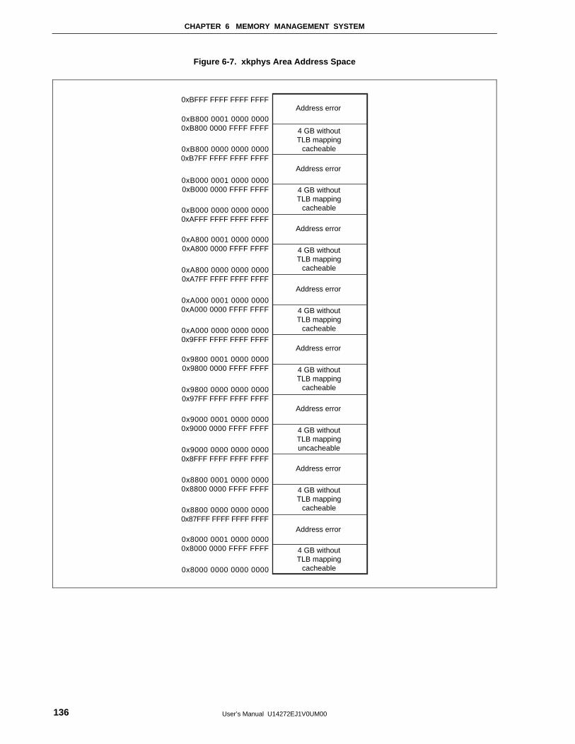
CHAPTER 6 MEMORY MANAGEMENT SYSTEM
User’s Manual U14272EJ1V0UM00136
Figure 6-7. xkphys Area Address Space
0xBFFF FFFF FFFF FFFF
0xB800 0000 0000 00000xB7FF FFFF FFFF FFFF
0xB000 0001 0000 00000xB000 0000 FFFF FFFF
0xB000 0000 0000 00000xAFFF FFFF FFFF FFFF
0xA800 0001 0000 00000xA800 0000 FFFF FFFF
0xA800 0000 0000 00000xA7FF FFFF FFFF FFFF
0xA000 0001 0000 00000xA000 0000 FFFF FFFF
0xA000 0000 0000 00000x9FFF FFFF FFFF FFFF
0x9800 0001 0000 00000x9800 0000 FFFF FFFF
0x9800 0000 0000 00000x97FF FFFF FFFF FFFF
0x9000 0001 0000 00000x9000 0000 FFFF FFFF
0x9000 0000 0000 00000x8FFF FFFF FFFF FFFF
0x8800 0001 0000 00000x8800 0000 FFFF FFFF
0x8800 0000 0000 00000x87FFF FFFF FFFF FFFF
0x8000 0001 0000 00000x8000 0000 FFFF FFFF
0x8000 0000 0000 0000
0xB800 0001 0000 00000xB800 0000 FFFF FFFF
Address error
4 GB withoutTLB mapping
cacheable
Address error
4 GB withoutTLB mapping
cacheable
Address error
4 GB withoutTLB mapping
cacheable
Address error
4 GB withoutTLB mapping
cacheable
Address error
4 GB withoutTLB mapping
cacheable
Address error
4 GB withoutTLB mappinguncacheable
Address error
4 GB withoutTLB mapping
cacheable
Address error
4 GB withoutTLB mapping
cacheable
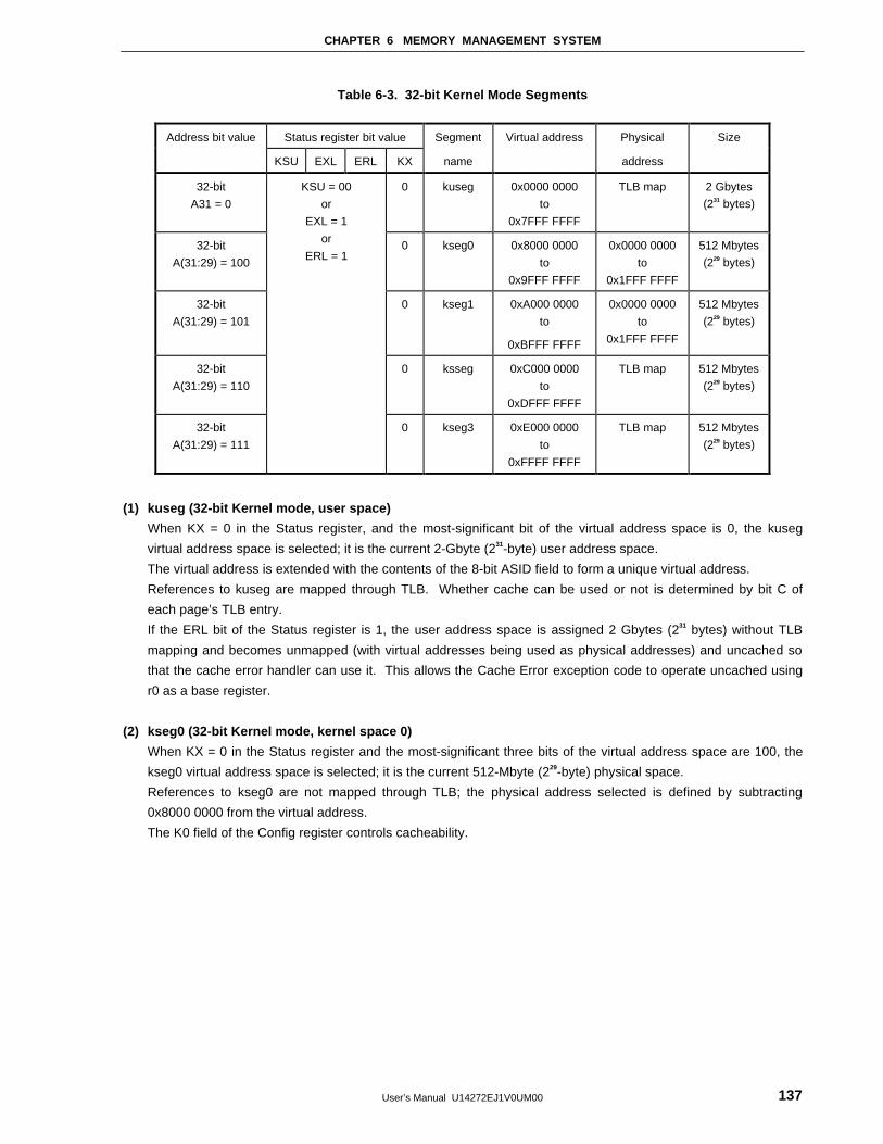
CHAPTER 6 MEMORY MANAGEMENT SYSTEM
User’s Manual U14272EJ1V0UM00 137
Table 6-3. 32-bit Kernel Mode Segments
Address bit value Status register bit value Segment Virtual address Physical Size
KSU EXL ERL KX name address
32-bit
A31 = 0
0 kuseg 0x0000 0000
to
0x7FFF FFFF
TLB map 2 Gbytes
(231 bytes)
32-bit
A(31:29) = 100
0 kseg0 0x8000 0000
to
0x9FFF FFFF
0x0000 0000
to
0x1FFF FFFF
512 Mbytes
(229 bytes)
32-bit
A(31:29) = 101
0 kseg1 0xA000 0000
to
0xBFFF FFFF
0x0000 0000
to
0x1FFF FFFF
512 Mbytes
(229 bytes)
32-bit
A(31:29) = 110
0 ksseg 0xC000 0000
to
0xDFFF FFFF
TLB map 512 Mbytes
(229 bytes)
32-bit
A(31:29) = 111
KSU = 00
or
EXL = 1
or
ERL = 1
0 kseg3 0xE000 0000
to
0xFFFF FFFF
TLB map 512 Mbytes
(229 bytes)
(1) kuseg (32-bit Kernel mode, user space)
When KX = 0 in the Status register, and the most-significant bit of the virtual address space is 0, the kuseg
virtual address space is selected; it is the current 2-Gbyte (231-byte) user address space.
The virtual address is extended with the contents of the 8-bit ASID field to form a unique virtual address.
References to kuseg are mapped through TLB. Whether cache can be used or not is determined by bit C of
each page’s TLB entry.
If the ERL bit of the Status register is 1, the user address space is assigned 2 Gbytes (231 bytes) without TLB
mapping and becomes unmapped (with virtual addresses being used as physical addresses) and uncached so
that the cache error handler can use it. This allows the Cache Error exception code to operate uncached using
r0 as a base register.
(2) kseg0 (32-bit Kernel mode, kernel space 0)
When KX = 0 in the Status register and the most-significant three bits of the virtual address space are 100, the
kseg0 virtual address space is selected; it is the current 512-Mbyte (229-byte) physical space.
References to kseg0 are not mapped through TLB; the physical address selected is defined by subtracting
0x8000 0000 from the virtual address.
The K0 field of the Config register controls cacheability.
CHAPTER 6 MEMORY MANAGEMENT SYSTEM
User’s Manual U14272EJ1V0UM00138
(3) kseg1 (32-bit Kernel mode, kernel space 1)
When KX = 0 in the Status register and the most-significant three bits of the virtual address space are 101, the
kseg1 virtual address space is selected; it is the current 512-Mbyte (229-byte) physical space.
References to kseg1 are not mapped through TLB; the physical address selected is defined by subtracting
0xA000 0000 from the virtual address.
Caches are disabled for accesses to these addresses, and main memory (or memory-mapped I/O device
registers) is accessed directly.
(4) ksseg (32-bit Kernel mode, supervisor space)
When KX = 0 in the Status register and the most-significant three bits of the virtual address space are 110, the
ksseg virtual address space is selected; it is the current 512-Mbyte (229-byte) virtual address space. The virtual
address is extended with the contents of the 8-bit ASID field to form a unique virtual address.
References to ksseg are mapped through TLB. Whether cache can be used or not is determined by bit C of
each page’s TLB entry.
(5) kseg3 (32-bit Kernel mode, kernel space 3)
When KX = 0 in the Status register and the most-significant three bits of the virtual address space are 111, the
kseg3 virtual address space is selected; it is the current 512-Mbyte (229-byte) kernel virtual space. The virtual
address is extended with the contents of the 8-bit ASID field to form a unique virtual address.
References to kseg3 are mapped through TLB. Whether cache can be used or not is determined by bit C of
each page’s TLB entry.
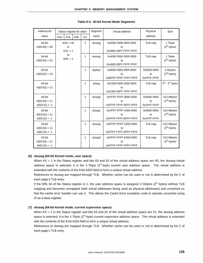
CHAPTER 6 MEMORY MANAGEMENT SYSTEM
User’s Manual U14272EJ1V0UM00 139
Table 6-4. 64-bit Kernel Mode Segments
Address bit Status register bit value Segment Virtual address Physical Size
value KSU EXL ERL KX name address
64-bit
A(63:62) = 00
1 xkuseg 0x0000 0000 0000 0000
to
0x0000 00FF FFFF FFFF
TLB map 1 Tbyte
(240 bytes)
64-bit
A(63:62) = 01
1 xksseg 0x4000 0000 0000 0000
to
0x4000 00FF FFFF FFFF
TLB map 1 Tbyte
(240 bytes)
64-bit
A(63:62) = 10
1 xkphys 0x8000 0000 0000 0000
to
0xBFFF FFFF FFFF FFFF
0x0000 0000
to
0xFFFF FFFF
4 Gbytes
(232 bytes)
64-bit
A(63:62) = 11
1 xkseg 0xC000 0000 0000 0000
to
0xC000 00FF 7FFF FFFF
TLB map 240 - 231 bytes
64-bit
A(63:62) = 11
A(63:31) = -1
1 ckseg0 0xFFFF FFFF 8000 0000
to
0xFFFF FFFF 9FFF FFFF
0x0000 0000
to
0x1FFF FFFF
512 Mbytes
(229 bytes)
64-bit
A(63:62) = 11
A(63:31) = -1
1 ckseg1 0xFFFF FFFF A000 0000
to
0xFFFF FFFF BFFF FFFF
0x0000 0000
to
0x1FFF FFFF
512 Mbytes
(229 bytes)
64-bit
A(63:62) = 11
A(63:31) = -1
1 cksseg 0xFFFF FFFF C000 0000
to
0xFFFF FFFF DFFF FFFF
TLB map 512 Mbytes
(229 bytes)
64-bit
A(63:62) = 11
A(63:31) = -1
KSU = 00
or
EXL = 1
or
ERL = 1
1 ckseg3 0xFFFF FFFF E000 0000
to
0xFFFF FFFF FFFF FFFF
TLB map 512 Mbytes
(229 bytes)
(6) xkuseg (64-bit Kernel mode, user space)
When KX = 1 in the Status register and bits 63 and 62 of the virtual address space are 00, the xkuseg virtual
address space is selected; it is the 1-Tbyte (240-byte) current user address space. The virtual address is
extended with the contents of the 8-bit ASID field to form a unique virtual address.
References to xkuseg are mapped through TLB. Whether cache can be used or not is determined by bit C of
each page’s TLB entry.
If the ERL bit of the Status register is 1, the user address space is assigned 2 Gbytes (231 bytes) without TLB
mapping and becomes unmapped (with virtual addresses being used as physical addresses) and uncached so
that the cache error handler can use it. This allows the Cache Error exception code to operate uncached using
r0 as a base register.
(7) xksseg (64-bit Kernel mode, current supervisor space)
When KX = 1 in the Status register and bits 63 and 62 of the virtual address space are 01, the xksseg address
space is selected; it is the 1-Tbyte (240-byte) current supervisor address space. The virtual address is extended
with the contents of the 8-bit ASID field to form a unique virtual address.
References to xksseg are mapped through TLB. Whether cache can be used or not is determined by bit C of
each page’s TLB entry.
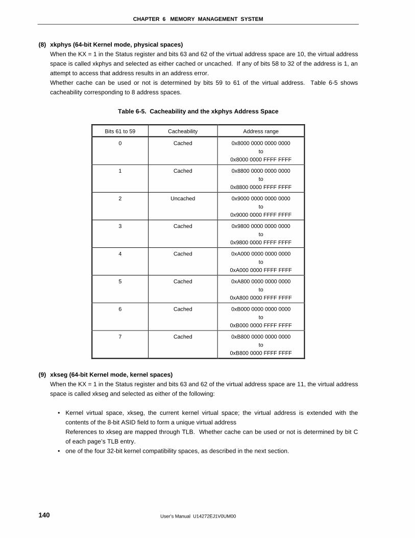
CHAPTER 6 MEMORY MANAGEMENT SYSTEM
User’s Manual U14272EJ1V0UM00140
(8) xkphys (64-bit Kernel mode, physical spaces)
When the KX = 1 in the Status register and bits 63 and 62 of the virtual address space are 10, the virtual address
space is called xkphys and selected as either cached or uncached. If any of bits 58 to 32 of the address is 1, an
attempt to access that address results in an address error.
Whether cache can be used or not is determined by bits 59 to 61 of the virtual address. Table 6-5 shows
cacheability corresponding to 8 address spaces.
Table 6-5. Cacheability and the xkphys Address Space
Bits 61 to 59 Cacheability Address range
0 Cached 0x8000 0000 0000 0000
to
0x8000 0000 FFFF FFFF
1 Cached 0x8800 0000 0000 0000
to
0x8800 0000 FFFF FFFF
2 Uncached 0x9000 0000 0000 0000
to
0x9000 0000 FFFF FFFF
3 Cached 0x9800 0000 0000 0000
to
0x9800 0000 FFFF FFFF
4 Cached 0xA000 0000 0000 0000
to
0xA000 0000 FFFF FFFF
5 Cached 0xA800 0000 0000 0000
to
0xA800 0000 FFFF FFFF
6 Cached 0xB000 0000 0000 0000
to
0xB000 0000 FFFF FFFF
7 Cached 0xB800 0000 0000 0000
to
0xB800 0000 FFFF FFFF
(9) xkseg (64-bit Kernel mode, kernel spaces)
When the KX = 1 in the Status register and bits 63 and 62 of the virtual address space are 11, the virtual address
space is called xkseg and selected as either of the following:
• Kernel virtual space, xkseg, the current kernel virtual space; the virtual address is extended with the
contents of the 8-bit ASID field to form a unique virtual address
References to xkseg are mapped through TLB. Whether cache can be used or not is determined by bit C
of each page’s TLB entry.
• one of the four 32-bit kernel compatibility spaces, as described in the next section.
CHAPTER 6 MEMORY MANAGEMENT SYSTEM
User’s Manual U14272EJ1V0UM00 141
(10)64-bit Kernel mode compatible spaces (ckseg0, ckseg1, cksseg, and ckseg3)
If the conditions listed below are satisfied in Kernel mode, ckseg0, ckseg1, cksseg, or ckseg3 (each having 512
Mbytes) is selected as a compatible space according to the state of the bits 30 and 29 (two low-order bits) of the
address.
• The KX bit of the Status register is 1.
• Bits 63 and 62 of the 64-bit virtual address are 11.
• Bits 61 to 31 of the virtual address are all 1.
(a) ckseg0
This space is an unmapped region, compatible with the 32-bit mode kseg0 space. The K0 field of the Config
register controls cacheability and coherency.
(b) ckseg1
This space is an unmapped and uncached region, compatible with the 32-bit mode kseg1 space.
(c) cksseg
This space is the current supervisor virtual space, compatible with the 32-bit mode ksseg space.
References to cksseg are mapped through TLB. Whether cache can be used or not is determined by bit C of
each page’s TLB entry.
(d) ckseg3
This space is the current supervisor virtual space, compatible with the 32-bit mode kseg3 space.
References to ckseg3 are mapped through TLB. Whether cache can be used or not is determined by bit C of
each page’s TLB entry.
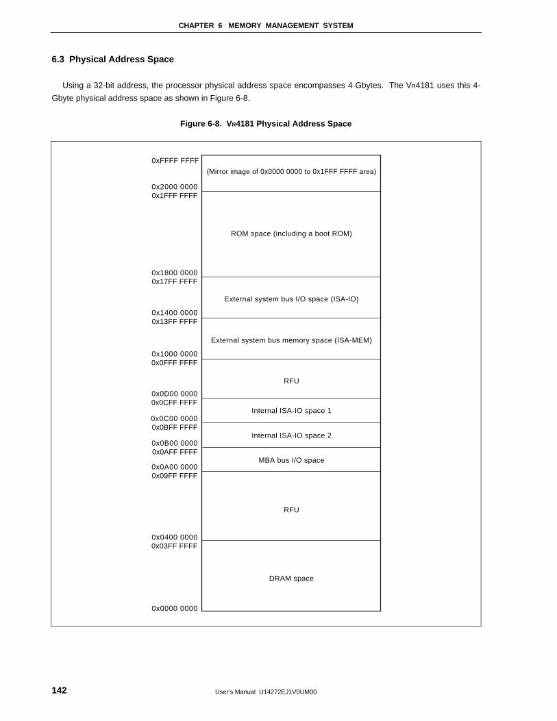
CHAPTER 6 MEMORY MANAGEMENT SYSTEM
User’s Manual U14272EJ1V0UM00142
6.3 Physical Address Space
Using a 32-bit address, the processor physical address space encompasses 4 Gbytes. The VR4181 uses this 4-
Gbyte physical address space as shown in Figure 6-8.
Figure 6-8. V R4181 Physical Address Space
0xFFFF FFFF
(Mirror image of 0x0000 0000 to 0x1FFF FFFF area)
ROM space (including a boot ROM)
External system bus memory space (ISA-MEM)
Internal ISA-IO space 1
Internal ISA-IO space 2
RFU
DRAM space
MBA bus I/O space
RFU
0x1800 00000x17FF FFFF
0x0C00 00000x0BFF FFFF
0x0B00 00000x0AFF FFFF
0x0D00 00000x0CFF FFFF
0x0A00 00000x09FF FFFF
0x0400 00000x03FF FFFF
0x0000 0000
0x1000 00000x0FFF FFFF
0x2000 00000x1FFF FFFF
External system bus I/O space (ISA-IO)
0x1400 00000x13FF FFFF
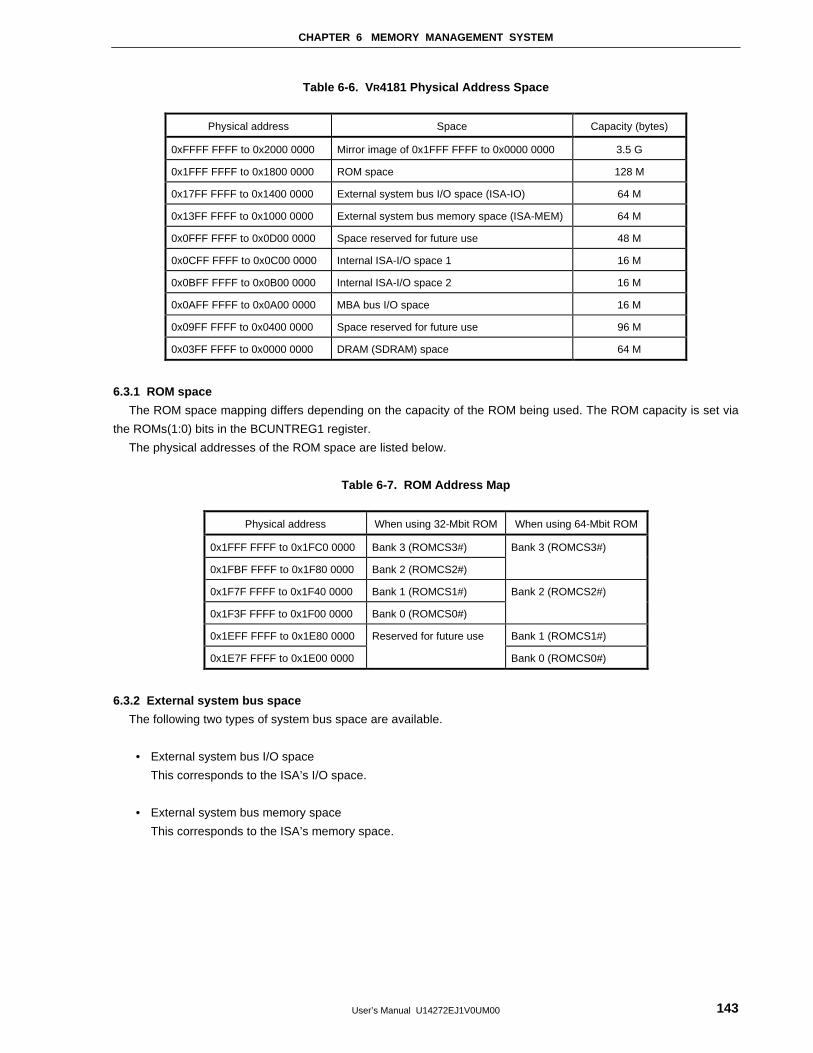
CHAPTER 6 MEMORY MANAGEMENT SYSTEM
User’s Manual U14272EJ1V0UM00 143
Table 6-6. VR4181 Physical Address Space
Physical address Space Capacity (bytes)
0xFFFF FFFF to 0x2000 0000 Mirror image of 0x1FFF FFFF to 0x0000 0000 3.5 G
0x1FFF FFFF to 0x1800 0000 ROM space 128 M
0x17FF FFFF to 0x1400 0000 External system bus I/O space (ISA-IO) 64 M
0x13FF FFFF to 0x1000 0000 External system bus memory space (ISA-MEM) 64 M
0x0FFF FFFF to 0x0D00 0000 Space reserved for future use 48 M
0x0CFF FFFF to 0x0C00 0000 Internal ISA-I/O space 1 16 M
0x0BFF FFFF to 0x0B00 0000 Internal ISA-I/O space 2 16 M
0x0AFF FFFF to 0x0A00 0000 MBA bus I/O space 16 M
0x09FF FFFF to 0x0400 0000 Space reserved for future use 96 M
0x03FF FFFF to 0x0000 0000 DRAM (SDRAM) space 64 M
6.3.1 ROM space
The ROM space mapping differs depending on the capacity of the ROM being used. The ROM capacity is set via
the ROMs(1:0) bits in the BCUNTREG1 register.
The physical addresses of the ROM space are listed below.
Table 6-7. ROM Address Map
Physical address When using 32-Mbit ROM When using 64-Mbit ROM
0x1FFF FFFF to 0x1FC0 0000 Bank 3 (ROMCS3#) Bank 3 (ROMCS3#)
0x1FBF FFFF to 0x1F80 0000 Bank 2 (ROMCS2#)
0x1F7F FFFF to 0x1F40 0000 Bank 1 (ROMCS1#) Bank 2 (ROMCS2#)
0x1F3F FFFF to 0x1F00 0000 Bank 0 (ROMCS0#)
0x1EFF FFFF to 0x1E80 0000 Reserved for future use Bank 1 (ROMCS1#)
0x1E7F FFFF to 0x1E00 0000 Bank 0 (ROMCS0#)
6.3.2 External system bus space
The following two types of system bus space are available.
• External system bus I/O space
This corresponds to the ISA’s I/O space.
• External system bus memory space
This corresponds to the ISA’s memory space.
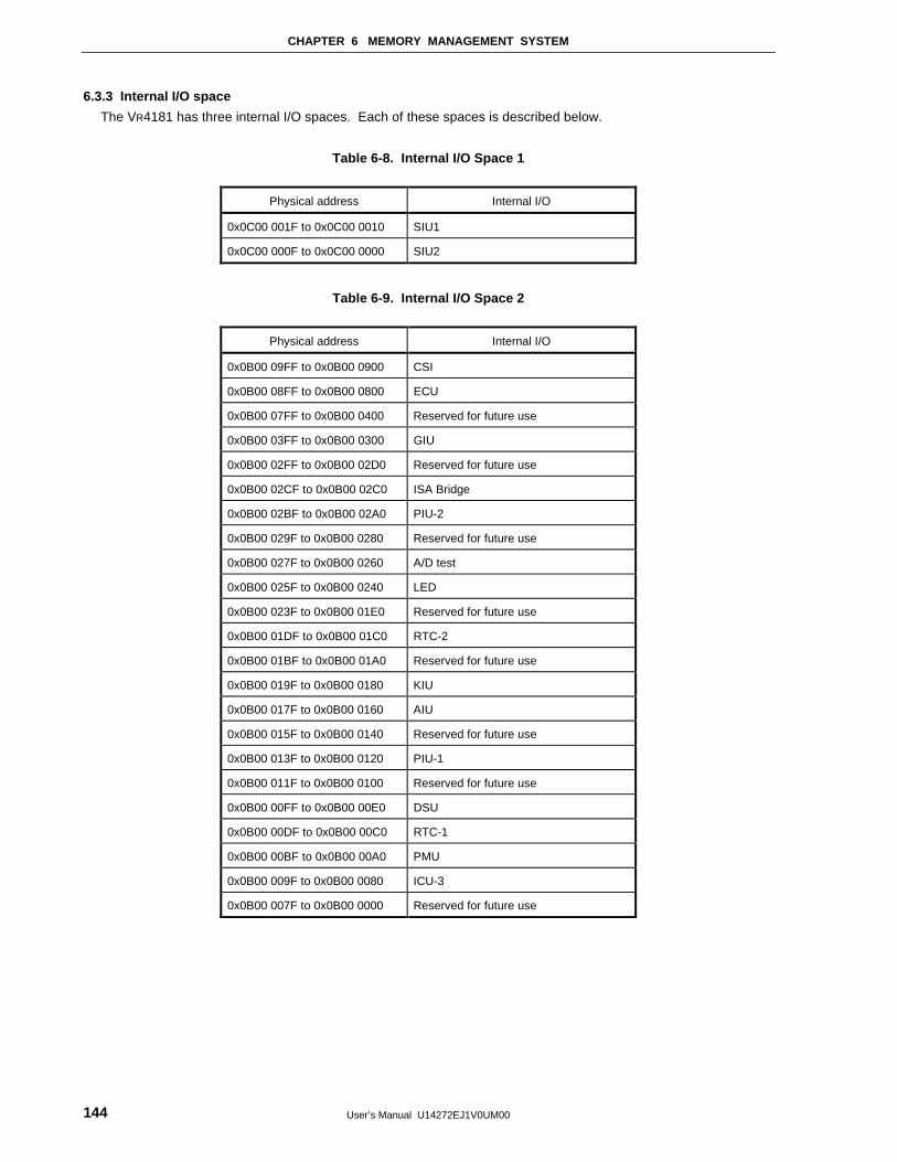
CHAPTER 6 MEMORY MANAGEMENT SYSTEM
User’s Manual U14272EJ1V0UM00144
6.3.3 Internal I/O space
The VR4181 has three internal I/O spaces. Each of these spaces is described below.
Table 6-8. Internal I/O Space 1
Physical address Internal I/O
0x0C00 001F to 0x0C00 0010 SIU1
0x0C00 000F to 0x0C00 0000 SIU2
Table 6-9. Internal I/O Space 2
Physical address Internal I/O
0x0B00 09FF to 0x0B00 0900 CSI
0x0B00 08FF to 0x0B00 0800 ECU
0x0B00 07FF to 0x0B00 0400 Reserved for future use
0x0B00 03FF to 0x0B00 0300 GIU
0x0B00 02FF to 0x0B00 02D0 Reserved for future use
0x0B00 02CF to 0x0B00 02C0 ISA Bridge
0x0B00 02BF to 0x0B00 02A0 PIU-2
0x0B00 029F to 0x0B00 0280 Reserved for future use
0x0B00 027F to 0x0B00 0260 A/D test
0x0B00 025F to 0x0B00 0240 LED
0x0B00 023F to 0x0B00 01E0 Reserved for future use
0x0B00 01DF to 0x0B00 01C0 RTC-2
0x0B00 01BF to 0x0B00 01A0 Reserved for future use
0x0B00 019F to 0x0B00 0180 KIU
0x0B00 017F to 0x0B00 0160 AIU
0x0B00 015F to 0x0B00 0140 Reserved for future use
0x0B00 013F to 0x0B00 0120 PIU-1
0x0B00 011F to 0x0B00 0100 Reserved for future use
0x0B00 00FF to 0x0B00 00E0 DSU
0x0B00 00DF to 0x0B00 00C0 RTC-1
0x0B00 00BF to 0x0B00 00A0 PMU
0x0B00 009F to 0x0B00 0080 ICU-3
0x0B00 007F to 0x0B00 0000 Reserved for future use
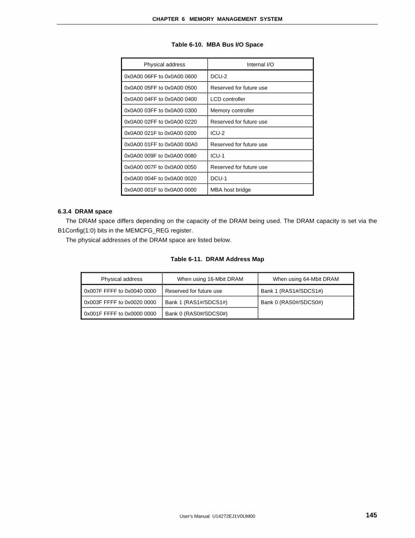
CHAPTER 6 MEMORY MANAGEMENT SYSTEM
User’s Manual U14272EJ1V0UM00 145
Table 6-10. MBA Bus I/O Space
Physical address Internal I/O
0x0A00 06FF to 0x0A00 0600 DCU-2
0x0A00 05FF to 0x0A00 0500 Reserved for future use
0x0A00 04FF to 0x0A00 0400 LCD controller
0x0A00 03FF to 0x0A00 0300 Memory controller
0x0A00 02FF to 0x0A00 0220 Reserved for future use
0x0A00 021F to 0x0A00 0200 ICU-2
0x0A00 01FF to 0x0A00 00A0 Reserved for future use
0x0A00 009F to 0x0A00 0080 ICU-1
0x0A00 007F to 0x0A00 0050 Reserved for future use
0x0A00 004F to 0x0A00 0020 DCU-1
0x0A00 001F to 0x0A00 0000 MBA host bridge
6.3.4 DRAM space
The DRAM space differs depending on the capacity of the DRAM being used. The DRAM capacity is set via the
B1Config(1:0) bits in the MEMCFG_REG register.
The physical addresses of the DRAM space are listed below.
Table 6-11. DRAM Address Map
Physical address When using 16-Mbit DRAM When using 64-Mbit DRAM
0x007F FFFF to 0x0040 0000 Reserved for future use Bank 1 (RAS1#/SDCS1#)
0x003F FFFF to 0x0020 0000 Bank 1 (RAS1#/SDCS1#) Bank 0 (RAS0#/SDCS0#)
0x001F FFFF to 0x0000 0000 Bank 0 (RAS0#/SDCS0#)
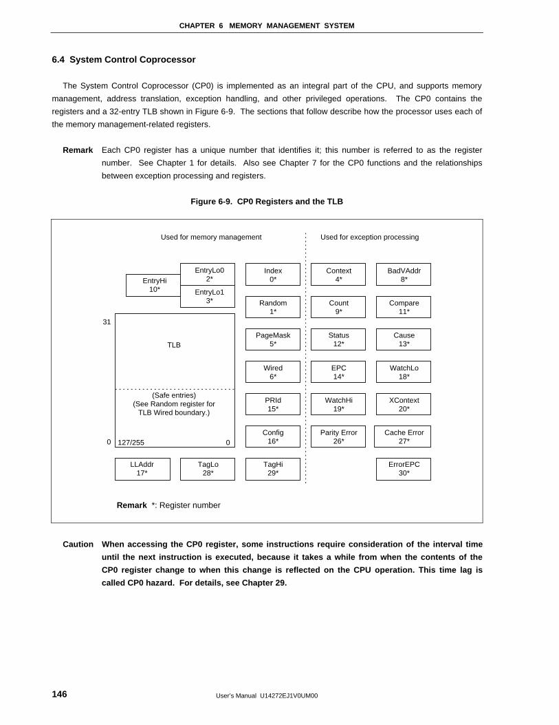
CHAPTER 6 MEMORY MANAGEMENT SYSTEM
User’s Manual U14272EJ1V0UM00146
6.4 System Control Coprocessor
The System Control Coprocessor (CP0) is implemented as an integral part of the CPU, and supports memory
management, address translation, exception handling, and other privileged operations. The CP0 contains the
registers and a 32-entry TLB shown in Figure 6-9. The sections that follow describe how the processor uses each of
the memory management-related registers.
Remark Each CP0 register has a unique number that identifies it; this number is referred to as the register
number. See Chapter 1 for details. Also see Chapter 7 for the CP0 functions and the relationships
between exception processing and registers.
Figure 6-9. CP0 Registers and the TLB
31
TLB
(Safe entries)(See Random register for
TLB Wired boundary.)
Used for memory management Used for exception processing
127/255 0
LLAddr17*
TagLo28*
TagHi29*
ErrorEPC30*
Config16*
Cache Error27*
PRId15*
XContext20*
Wired6*
WatchLo18*
PageMask5*
Cause13*
Random1*
Compare11*
Index0*
EntryLo02*
EntryLo13*
EntryHi10*
BadVAddr8*
Parity Error26*
WatchHi19*
EPC14*
Status12*
Count9*
Context4*
0
Remark *: Register number
Caution When accessing the CP0 register, some instructions require consideration of the interval time
until the next instruction is executed, because it takes a while from when the contents of the
CP0 register change to when this change is reflected on the CPU operation. This time lag is
called CP0 hazard. For details, see Chapter 29.
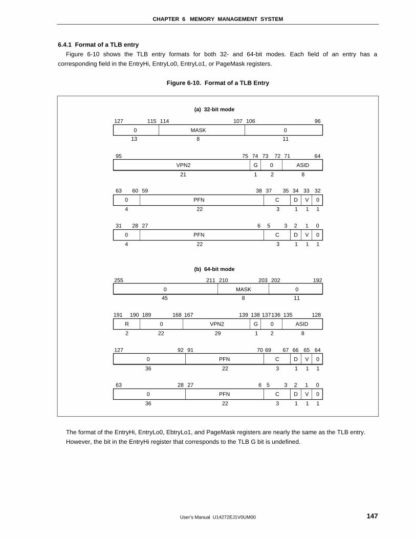
CHAPTER 6 MEMORY MANAGEMENT SYSTEM
User’s Manual U14272EJ1V0UM00 147
6.4.1 Format of a TLB entry
Figure 6-10 shows the TLB entry formats for both 32- and 64-bit modes. Each field of an entry has a
corresponding field in the EntryHi, EntryLo0, EntryLo1, or PageMask registers.
Figure 6-10. Format of a TLB Entry
127
13
0 MASK
(a) 32-bit mode
(b) 64-bit mode
0
8 11
115 114
95
21 1 2 8
VPN2
63 60 59 38 37 35 34 33 32
4 22 3 1 1 1
PFN C D V 00
31 28 27 6 5 3 2 1 0
4 22 3 1 1 1
PFN C D V 00
63 28 27 6 5 3 2 1 0
36 22 3 1 1 1
PFN C D V 00
127 92 91 70 69 67 66 65 64
36 22 3 1 1 1
PFN C D V 00
191 168 167190 189 139 137138 136 135 128
2 22 29 1 2 8
VPN2 G 0 ASID0R
G 0 ASID
75 73 72 71 6474
107 106 96
255
45
0 MASK 0
8 11
211 210 203 202 192
The format of the EntryHi, EntryLo0, EbtryLo1, and PageMask registers are nearly the same as the TLB entry.
However, the bit in the EntryHi register that corresponds to the TLB G bit is undefined.
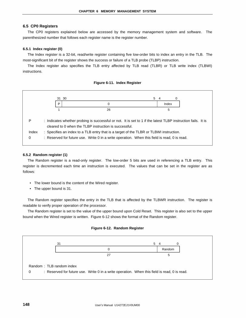
CHAPTER 6 MEMORY MANAGEMENT SYSTEM
User’s Manual U14272EJ1V0UM00148
6.5 CP0 RegistersThe CP0 registers explained below are accessed by the memory management system and software. The
parenthesized number that follows each register name is the register number.
6.5.1 Index register (0)
The Index register is a 32-bit, read/write register containing five low-order bits to index an entry in the TLB. The
most-significant bit of the register shows the success or failure of a TLB probe (TLBP) instruction.
The Index register also specifies the TLB entry affected by TLB read (TLBR) or TLB write index (TLBWI)
instructions.
Figure 6-11. Index Register
31
P 0
1 26
Index
5
30 5 4 0
P : Indicates whether probing is successful or not. It is set to 1 if the latest TLBP instruction fails. It is
cleared to 0 when the TLBP instruction is successful.
Index : Specifies an index to a TLB entry that is a target of the TLBR or TLBWI instruction.
0 : Reserved for future use. Write 0 in a write operation. When this field is read, 0 is read.
6.5.2 Random register (1)
The Random register is a read-only register. The low-order 5 bits are used in referencing a TLB entry. This
register is decremented each time an instruction is executed. The values that can be set in the register are as
follows:
• The lower bound is the content of the Wired register.
• The upper bound is 31.
The Random register specifies the entry in the TLB that is affected by the TLBWR instruction. The register is
readable to verify proper operation of the processor.
The Random register is set to the value of the upper bound upon Cold Reset. This register is also set to the upper
bound when the Wired register is written. Figure 6-12 shows the format of the Random register.
Figure 6-12. Random Register
31
0
27
Random
5
5 4 0
Random : TLB random index
0 : Reserved for future use. Write 0 in a write operation. When this field is read, 0 is read.
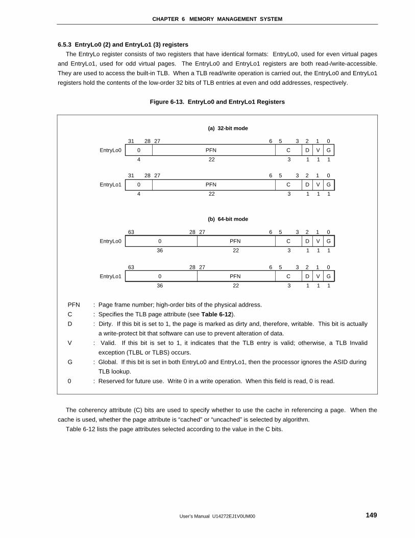
CHAPTER 6 MEMORY MANAGEMENT SYSTEM
User’s Manual U14272EJ1V0UM00 149
6.5.3 EntryLo0 (2) and EntryLo1 (3) registers
The EntryLo register consists of two registers that have identical formats: EntryLo0, used for even virtual pages
and EntryLo1, used for odd virtual pages. The EntryLo0 and EntryLo1 registers are both read-/write-accessible.
They are used to access the built-in TLB. When a TLB read/write operation is carried out, the EntryLo0 and EntryLo1
registers hold the contents of the low-order 32 bits of TLB entries at even and odd addresses, respectively.
Figure 6-13. EntryLo0 and EntryLo1 Registers
(a) 32-bit mode
(b) 64-bit mode
31 28 27 6 5 3 2 1 0
4 22 3 1 1 1
PFN C D V G0EntryLo0
31 28 27 6 5 3 2 1 0
4 22 3 1 1 1
PFN C D V G0EntryLo1
63 28 27 6 5 3 2 1 0
36 22 3 1 1 1
PFN C D V G0EntryLo0
63 28 27 6 5 3 2 1 0
36 22 3 1 1 1
PFN C D V G0EntryLo1
PFN : Page frame number; high-order bits of the physical address.
C : Specifies the TLB page attribute (see Table 6-12 ).
D : Dirty. If this bit is set to 1, the page is marked as dirty and, therefore, writable. This bit is actually
a write-protect bit that software can use to prevent alteration of data.
V : Valid. If this bit is set to 1, it indicates that the TLB entry is valid; otherwise, a TLB Invalid
exception (TLBL or TLBS) occurs.
G : Global. If this bit is set in both EntryLo0 and EntryLo1, then the processor ignores the ASID during
TLB lookup.
0 : Reserved for future use. Write 0 in a write operation. When this field is read, 0 is read.
The coherency attribute (C) bits are used to specify whether to use the cache in referencing a page. When the
cache is used, whether the page attribute is “cached” or “uncached” is selected by algorithm.
Table 6-12 lists the page attributes selected according to the value in the C bits.
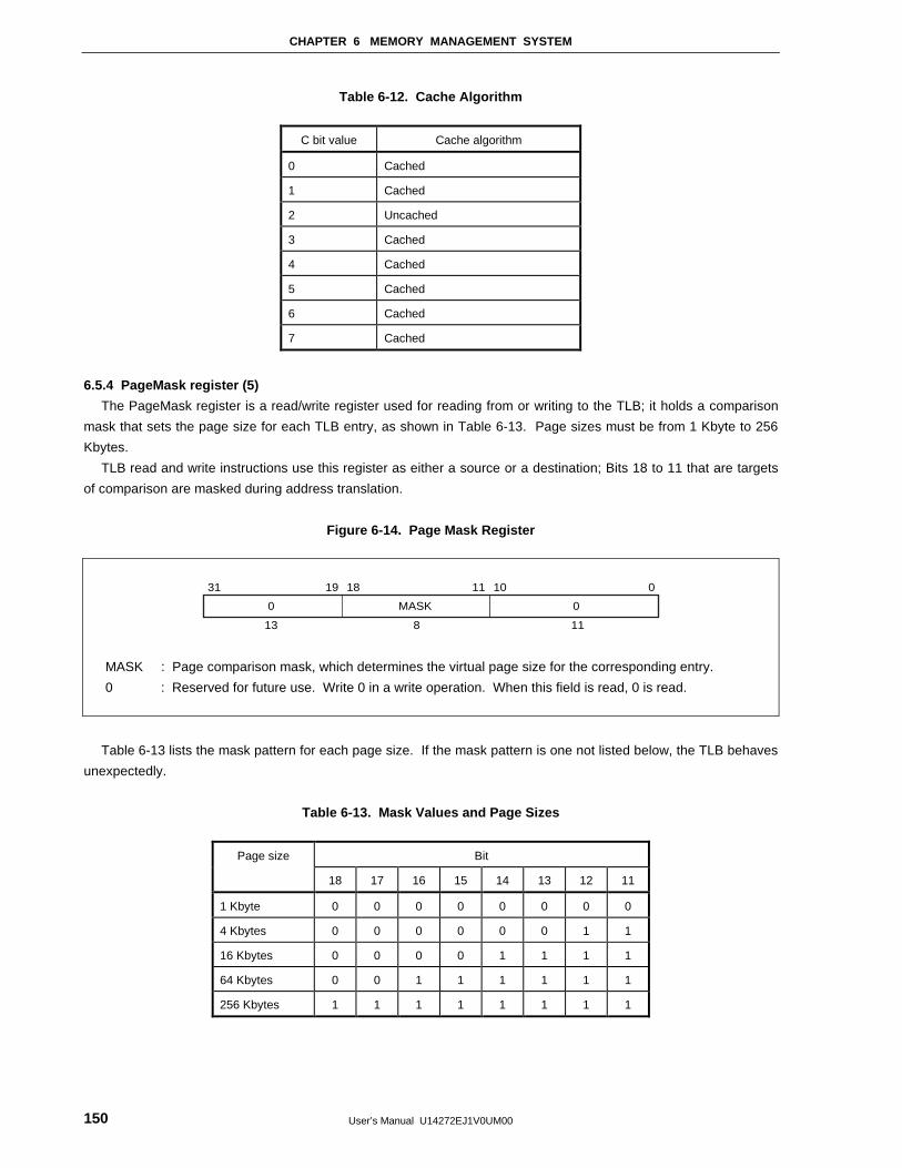
CHAPTER 6 MEMORY MANAGEMENT SYSTEM
User’s Manual U14272EJ1V0UM00150
Table 6-12. Cache Algorithm
C bit value Cache algorithm
0 Cached
1 Cached
2 Uncached
3 Cached
4 Cached
5 Cached
6 Cached
7 Cached
6.5.4 PageMask register (5)
The PageMask register is a read/write register used for reading from or writing to the TLB; it holds a comparison
mask that sets the page size for each TLB entry, as shown in Table 6-13. Page sizes must be from 1 Kbyte to 256
Kbytes.
TLB read and write instructions use this register as either a source or a destination; Bits 18 to 11 that are targets
of comparison are masked during address translation.
Figure 6-14. Page Mask Register
31 19 18 11 10 0
13 8 11
MASK 00
MASK : Page comparison mask, which determines the virtual page size for the corresponding entry.
0 : Reserved for future use. Write 0 in a write operation. When this field is read, 0 is read.
Table 6-13 lists the mask pattern for each page size. If the mask pattern is one not listed below, the TLB behaves
unexpectedly.
Table 6-13. Mask Values and Page Sizes
Page size Bit
18 17 16 15 14 13 12 11
1 Kbyte 0 0 0 0 0 0 0 0
4 Kbytes 0 0 0 0 0 0 1 1
16 Kbytes 0 0 0 0 1 1 1 1
64 Kbytes 0 0 1 1 1 1 1 1
256 Kbytes 1 1 1 1 1 1 1 1
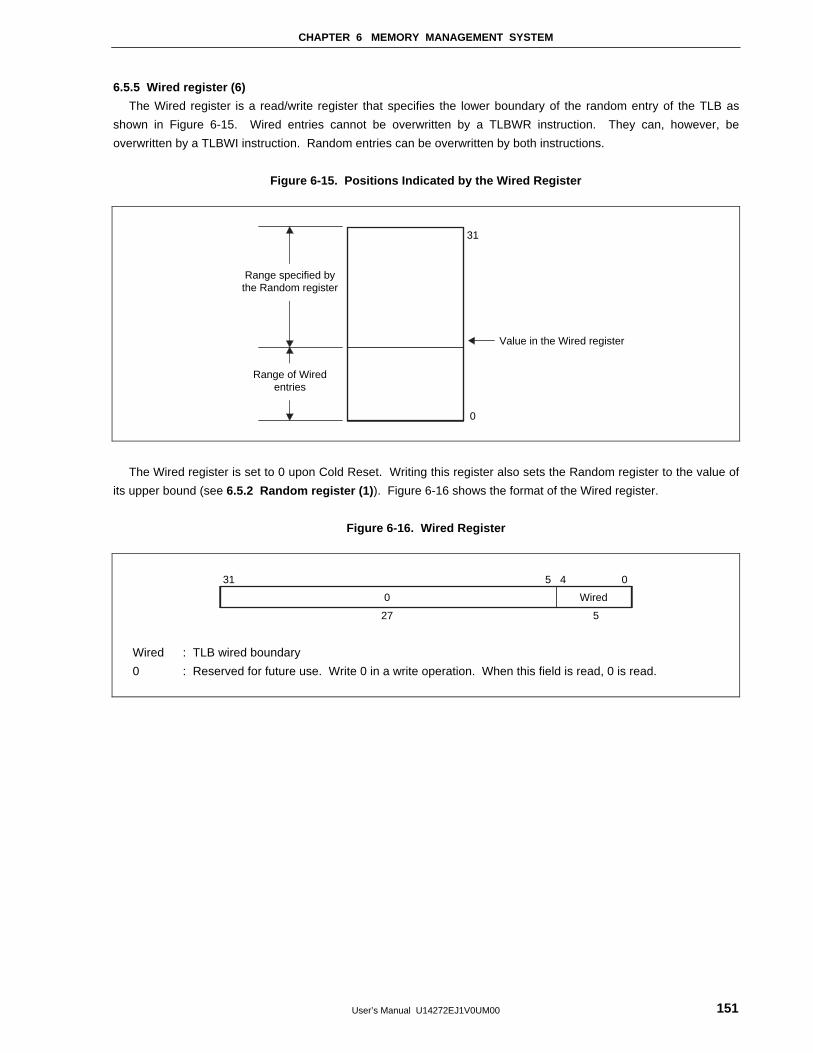
CHAPTER 6 MEMORY MANAGEMENT SYSTEM
User’s Manual U14272EJ1V0UM00 151
6.5.5 Wired register (6)
The Wired register is a read/write register that specifies the lower boundary of the random entry of the TLB as
shown in Figure 6-15. Wired entries cannot be overwritten by a TLBWR instruction. They can, however, be
overwritten by a TLBWI instruction. Random entries can be overwritten by both instructions.
Figure 6-15. Positions Indicated by the Wired Register
31
Value in the Wired register
0
Range specified bythe Random register
Range of Wiredentries
The Wired register is set to 0 upon Cold Reset. Writing this register also sets the Random register to the value of
its upper bound (see 6.5.2 Random register (1) ). Figure 6-16 shows the format of the Wired register.
Figure 6-16. Wired Register
31 5 4 0
27 5
0 Wired
Wired : TLB wired boundary
0 : Reserved for future use. Write 0 in a write operation. When this field is read, 0 is read.
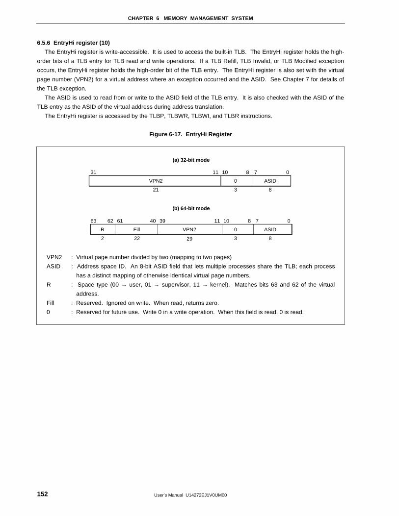
CHAPTER 6 MEMORY MANAGEMENT SYSTEM
User’s Manual U14272EJ1V0UM00152
6.5.6 EntryHi register (10)
The EntryHi register is write-accessible. It is used to access the built-in TLB. The EntryHi register holds the high-
order bits of a TLB entry for TLB read and write operations. If a TLB Refill, TLB Invalid, or TLB Modified exception
occurs, the EntryHi register holds the high-order bit of the TLB entry. The EntryHi register is also set with the virtual
page number (VPN2) for a virtual address where an exception occurred and the ASID. See Chapter 7 for details of
the TLB exception.
The ASID is used to read from or write to the ASID field of the TLB entry. It is also checked with the ASID of the
TLB entry as the ASID of the virtual address during address translation.
The EntryHi register is accessed by the TLBP, TLBWR, TLBWI, and TLBR instructions.
Figure 6-17. EntryHi Register
31 11 10 8 7 0
21
(a) 32-bit mode
(b) 64-bit mode
VPN2
3
0
8
ASID
63 62 61 11 1040 39 8 7 0
2 22
Fill
29
VPN2R
3
0
8
ASID
VPN2 : Virtual page number divided by two (mapping to two pages)
ASID : Address space ID. An 8-bit ASID field that lets multiple processes share the TLB; each process
has a distinct mapping of otherwise identical virtual page numbers.
R : Space type (00 → user, 01 → supervisor, 11 → kernel). Matches bits 63 and 62 of the virtual
address.
Fill : Reserved. Ignored on write. When read, returns zero.
0 : Reserved for future use. Write 0 in a write operation. When this field is read, 0 is read.
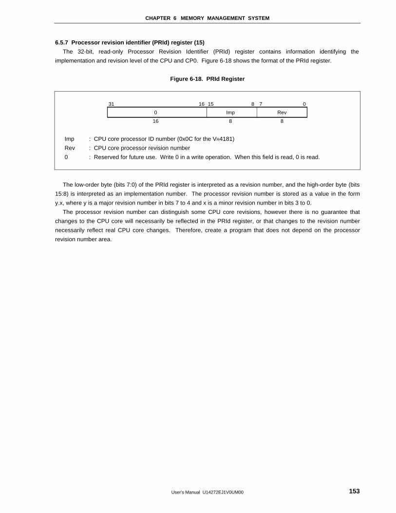
CHAPTER 6 MEMORY MANAGEMENT SYSTEM
User’s Manual U14272EJ1V0UM00 153
6.5.7 Processor revision identifier (PRId) register (15)
The 32-bit, read-only Processor Revision Identifier (PRId) register contains information identifying the
implementation and revision level of the CPU and CP0. Figure 6-18 shows the format of the PRId register.
Figure 6-18. PRId Register
31 16 15 8 7 0
16
0
8
Imp
8
Rev
Imp : CPU core processor ID number (0x0C for the VR4181)
Rev : CPU core processor revision number
0 : Reserved for future use. Write 0 in a write operation. When this field is read, 0 is read.
The low-order byte (bits 7:0) of the PRId register is interpreted as a revision number, and the high-order byte (bits
15:8) is interpreted as an implementation number. The processor revision number is stored as a value in the form
y.x, where y is a major revision number in bits 7 to 4 and x is a minor revision number in bits 3 to 0.
The processor revision number can distinguish some CPU core revisions, however there is no guarantee that
changes to the CPU core will necessarily be reflected in the PRId register, or that changes to the revision number
necessarily reflect real CPU core changes. Therefore, create a program that does not depend on the processor
revision number area.
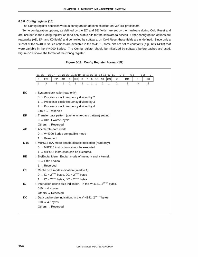
CHAPTER 6 MEMORY MANAGEMENT SYSTEM
User’s Manual U14272EJ1V0UM00154
6.5.8 Config register (16)
The Config register specifies various configuration options selected on VR4181 processors.
Some configuration options, as defined by the EC and BE fields, are set by the hardware during Cold Reset and
are included in the Config register as read-only status bits for the software to access. Other configuration options are
read/write (AD, EP, and K0 fields) and controlled by software; on Cold Reset these fields are undefined. Since only a
subset of the VR4000 Series options are available in the VR4181, some bits are set to constants (e.g., bits 14:13) that
were variable in the VR4000 Series. The Config register should be initialized by software before caches are used.
Figure 6-19 shows the format of the Config register.
Figure 6-19. Config Register Format (1/2)
31 30 28 27 24 23 22 21 2019 18 17 16 15 14 13 12 11 9 8 6 5 3 2 0
0 EC EP AD 0 M16 0 1 0 BE 10 CS IC DC 0 K0
1 3 4 1 2 1 2 1 1 1 2 1 3 3 3 3
EC : System clock ratio (read only)
0 → Processor clock frequency divided by 2
1 → Processor clock frequency divided by 3
2 → Processor clock frequency divided by 4
3 to 7 → Reserved
EP : Transfer data pattern (cache write-back pattern) setting
0 → DD: 1 word/1 cycle
Others → Reserved
AD : Accelerate data mode
0 → VR4000 Series compatible mode
1 → Reserved
M16 : MIPS16 ISA mode enable/disable indication (read only)
0 → MIPS16 instruction cannot be executed
1 → MIPS16 instruction can be executed.
BE : BigEndianMem. Endian mode of memory and a kernel.
0 → Little endian
1 → Reserved
CS : Cache size mode indication (fixed to 1)
0 → IC = 2(n+12) bytes, DC = 2(n+12) bytes
1 → IC = 2(n+10) bytes, DC = 2(n+10) bytes
IC : Instruction cache size indication. In the VR4181, 2(IC+10) bytes.
010 → 4 Kbytes
Others → Reserved
DC : Data cache size indication. In the VR4181, 2(DC+10) bytes.
010 → 4 Kbytes
Others → Reserved
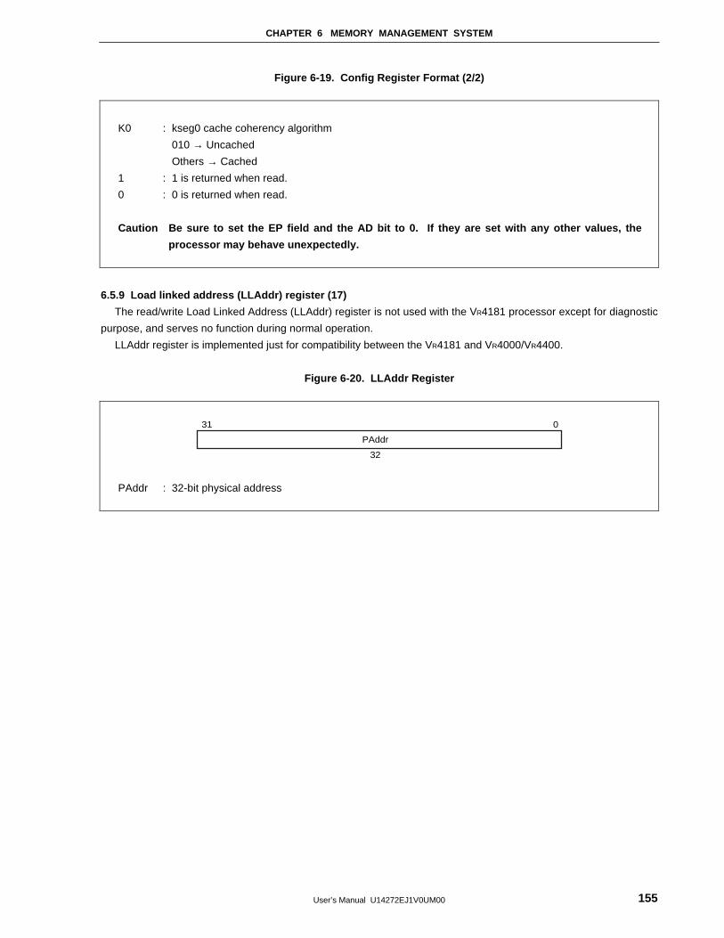
CHAPTER 6 MEMORY MANAGEMENT SYSTEM
User’s Manual U14272EJ1V0UM00 155
Figure 6-19. Config Register Format (2/2)
K0 : kseg0 cache coherency algorithm
010 → Uncached
Others → Cached
1 : 1 is returned when read.
0 : 0 is returned when read.
Caution Be sure to set the EP field and the AD bit to 0. If they are set with any other values, the
processor may behave unexpectedly.
6.5.9 Load linked address (LLAddr) register (17)
The read/write Load Linked Address (LLAddr) register is not used with the VR4181 processor except for diagnostic
purpose, and serves no function during normal operation.
LLAddr register is implemented just for compatibility between the VR4181 and VR4000/VR4400.
Figure 6-20. LLAddr Register
31 0
32
PAddr
PAddr : 32-bit physical address
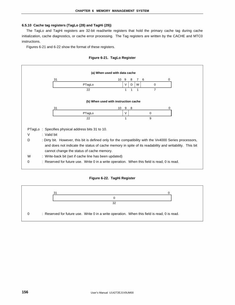
CHAPTER 6 MEMORY MANAGEMENT SYSTEM
User’s Manual U14272EJ1V0UM00156
6.5.10 Cache tag registers (TagLo (28) and TagHi (29))
The TagLo and TagHi registers are 32-bit read/write registers that hold the primary cache tag during cache
initialization, cache diagnostics, or cache error processing. The Tag registers are written by the CACHE and MTC0
instructions.
Figures 6-21 and 6-22 show the format of these registers.
Figure 6-21. TagLo Register
31 10 9 8 7 6 0
PTagLo
(a) When used with data cache
V D W 0
22 1 1 1 7
31 10 9 8 0
PTagLo
(b) When used with instruction cache
V 0
22 1 9
PTagLo : Specifies physical address bits 31 to 10.
V : Valid bit
D : Dirty bit. However, this bit is defined only for the compatibility with the VR4000 Series processors,
and does not indicate the status of cache memory in spite of its readability and writability. This bit
cannot change the status of cache memory.
W : Write-back bit (set if cache line has been updated)
0 : Reserved for future use. Write 0 in a write operation. When this field is read, 0 is read.
Figure 6-22. TagHi Register
31 0
32
0
0 : Reserved for future use. Write 0 in a write operation. When this field is read, 0 is read.
CHAPTER 6 MEMORY MANAGEMENT SYSTEM
User’s Manual U14272EJ1V0UM00 157
6.5.11 Virtual-to-physical address translation
During virtual-to-physical address translation, the CPU compares the 8-bit ASID (when the Global bit, G, is not set
to 1) of the virtual address to the ASID of the TLB entry to see if there is a match. One of the following comparisons
are also made:
• In 32-bit mode, the high-order bitsNote of the 32-bit virtual address are compared to the contents of the VPN2
(virtual page number divided by two) of each TLB entry.
• In 64-bit mode, the high-order bitsNote of the 64-bit virtual address are compared to the contents of the VPN2
(virtual page number divided by two) of each TLB entry.
If a TLB entry matches, the physical address and access control bits (C, D, and V) are retrieved from the matching
TLB entry. While the V bit of the entry must be set to 1 for a valid address translation to take place, it is not involved
in the determination of a matching TLB entry.
Figure 6-23 illustrates the TLB address translation flow.
Note The number of bits differs from page sizes. The table below shows the examples of high-order bits of the
virtual address in page size of 256 Kbytes and 1 Kbytes.
Page size
Mode
256 Kbytes 1 Kbytes
32-bit mode bits 31 to 19 bits 31 to 11
64-bit mode bits 63, 62, 39 to 19 bits 63, 62, 39 to 11
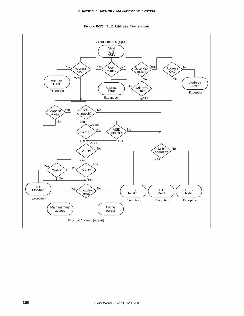
CHAPTER 6 MEMORY MANAGEMENT SYSTEM
User’s Manual U14272EJ1V0UM00158
Figure 6-23. TLB Address Translation
Virtual address (input)
Exception
ExceptionException Exception Exception
ExceptionException
No
No
NoNo
No
No
No
No
No
NoDirty
Valid
Global
No
No
No
No
Yes
YesYes
Yes
Yes
Yes
Yes
Yes
Yes
Yes
Yes
Yes
Yes
Yes
VPNand
ASID
AddressError
AddressError
Mappedarea?
VPNmatch?
G = 1?ASID
match?
32-bitaddress?V = 1?
D = 1?
Physical Address (output)
Write?
Uncachedarea?
Main memoryaccess
TLBModified TLB
InvalidTLBRefill
XTLBRefill
Cacheaccess
AddressError
AddressOK?
AddressOK?
AddressOK?
Supervisormode?
Usermode?
CHAPTER 6 MEMORY MANAGEMENT SYSTEM
User’s Manual U14272EJ1V0UM00 159
6.5.12 TLB misses
If there is no TLB entry that matches the virtual address, a TLB Refill (miss) exception occursNote. If the access
control bits (D and V) indicate that the access is not valid, a TLB Modified or TLB Invalid exception occurs. If the C
bit is 010, the retrieved physical address directly accesses main memory, bypassing the cache.
Note See Chapter 7 for details of the TLB Miss exception.
6.5.13 TLB instructions
The instructions used for TLB control are described below.
(1) Translation lookaside buffer probe (TLBP)
The translation lookaside buffer probe (TLBP) instruction loads the Index register with a TLB number that
matches the content of the EntryHi register. If there is no TLB number that matches the TLB entry, the highest-
order bit of the Index register is set.
(2) Translation lookaside buffer read (TLBR)
The translation lookaside buffer read (TLBR) instruction loads the EntryHi, EntryLo0, EntryLo1, and PageMask
registers with the content of the TLB entry indicated by the content of the Index register.
(3) Translation lookaside buffer write index (TLBWI)
The translation lookaside buffer write index (TLBWI) instruction writes the contents of the EntryHi, EntryLo0,
EntryLo1, and PageMask registers to the TLB entry indicated by the content of the Index register.
(4) Translation lookaside buffer write random (TLBWR)
The translation lookaside buffer write random (TLBWR) instruction writes the contents of the EntryHi, EntryLo0,
EntryLo1, and PageMask registers to the TLB entry indicated by the content of the Random register.

User’s Manual U14272EJ1V0UM00160
[MEMO]
User’s Manual U14272EJ1V0UM00 161
CHAPTER 7 EXCEPTION PROCESSING
This chapter describes CPU exception processing, including an explanation of hardware that processes
exceptions, followed by the format and use of each CPU exception register.
7.1 Exception Processing Operation
The processor receives exceptions from a number of sources, including translation lookaside buffer (TLB) misses,
arithmetic overflows, I/O interrupts, and system calls. When the CPU detects an exception, the normal sequence of
instruction execution is suspended and the processor enters Kernel mode (see Chapter 6 for a description of system
operating modes). If an exception occurs while executing a MIPS16 instruction, the processor stops the MIPS16
instruction execution, and shifts to the 32-bit instruction execution mode.
The processor then disables interrupts and transfers control for execution to the exception handler (located at a
specific address as an exception handling routine implemented by software). The handler saves the context of the
processor, including the contents of the program counter, the current operating mode (User or Supervisor), statuses,
and interrupt enabling. This context is saved so it can be restored when the exception has been serviced.
When an exception occurs, the CPU loads the Exception Program Counter (EPC) register with a location where
execution can restart after the exception has been serviced. The restart location in the EPC register is the address of
the instruction that caused the exception or, if the instruction was executing in a branch delay slot, the address of the
branch instruction immediately preceding the delay slot. Note that no branch delay slot generated by executing a
branch instruction exists when the processor operates in the MIPS16 mode.
When MIPS16 instructions are enabled to be executed, bit 0 of the EPC register indicates the operating mode in
which an exception occurred. It indicates 1 when in the MIPS16 instruction mode, and indicates 0 when in the MIPS
III instruction mode.
The VR4181 processor supports a Supervisor mode and fast TLB refill for all address spaces. The VR4181 also
provides the following functions:
• Interrupt enable (IE) bit
• Operating mode (User, Supervisor, or Kernel)
• Exception level (normal or exception is indicated by the EXL bit in the Status register)
• Error level (normal or error is indicated by the ERL bit in the Status register).
Interrupts are enabled when the following conditions are satisfied:
(1) Interrupt enable
An interrupt is enabled when the following conditions are satisfied.
• Interrupt enable bit (IE) = 1
• EXL bit = 0, ERL bit = 0
• Corresponding IM field bits in the Status register = 1
CHAPTER 7 EXCEPTION PROCESSING
User’s Manual U14272EJ1V0UM00162
(2) Operating mode
The operating mode is specified by KSU bit in the Status register when both the exception level and error level
are normal (0). The operation enters Kernel mode when either EXL bit or ERL bit in the Status register is set to
1.
(3) Exception/error levels
Returning from an exception resets the exception level to normal (0) (for details, see Chapter 27).
The registers that retain address, cause, and status information during exception processing are described in 7.3
Exception Processing Registers . For a description of the exception process, see 7.4 Details of Exceptions .
7.2 Precision of Exceptions
VR4181 exceptions are logically precise; the instruction that causes an exception and all those that follow it are
aborted and can be re-executed after servicing the exception. When succeeding instructions are killed, exceptions
associated with those instructions are also killed. Exceptions are not taken in the order detected, but in instruction
fetch order.
The exception handler can still determine exception and its origin. The cause of the program can be restarted by
rewriting the destination register - not automatically, however, as in the case of all the other precise exceptions where
no status change occurs.
CHAPTER 7 EXCEPTION PROCESSING
User’s Manual U14272EJ1V0UM00 163
7.3 Exception Processing Registers
This section describes the CP0 registers that are used in exception processing. Table 7-1 lists these registers,
along with their number-each register has a unique identification number that is referred to as its register number.
The CP0 registers not listed in the table are used in memory management (see Chapter 6 for details).
The exception handler examines the CP0 registers during exception processing to determine the cause of the
exception and the state of the CPU at the time the exception occurred.
The registers in Table 7-1 are used in exception processing, and are described in the sections that follow.
Table 7-1. CP0 Exception Processing Registers
Register name Register number
Context register 4
BadVAddr register 8
Count register 9
Compare register 11
Status register 12
Cause register 13
EPC register 14
WatchLo register 18
WatchHi register 19
XContext register 20
Parity Error registerNote
26
Cache Error registerNote
27
ErrorEPC register 30
Note This register is prepared to maintain compatibility
with the VR4100. This register is not used in the
VR4181 hardware.
CHAPTER 7 EXCEPTION PROCESSING
User’s Manual U14272EJ1V0UM00164
7.3.1 Context register (4)
The Context register is a read/write register containing the pointer to an entry in the page table entry (PTE) array
on the memory; this array is a table that stores virtual-to-physical address translations. When there is a TLB miss,
the operating system loads the unsuccessfully translated entry from the PTE array to the TLB. The Context register
is used by the TLB Refill exception handler for loading TLB entries. The Context register duplicates some of the
information provided in the BadVAddr register, but the information is arranged in a form that is more useful for a
software TLB exception handler. Figure 7-1 shows the format of the Context register.
Figure 7-1. Context Register Format
421
(a) 32-bit mode
(b) 64-bit mode
7
0
24
242531 4 3
PTEBase BadVPN2 0
42139
02563 4 3
PTEBase BadVPN2 0
PTEBase: The PTEBase field is a base address of the PTE entry table.
BadVPN2: The BadVPN2 field is written by hardware if a TLB miss occurs. This field holds the value (VPN2)
obtained by halving the virtual page number of the most recent virtual address for which
translation failed.
0: Reserved for future use. Write 0 in a write operation. When this field is read, 0 is read.
The PTEBase field is used by software as the pointer to the base address of the PTE table in the current user
address space.
The 21-bit BadVPN2 field contains bits 31 to 11 of the virtual address that caused the TLB miss; bit 10 is excluded
because a single TLB entry maps to an even-odd page pair. For a 1-Kbyte page size, this format can directly
address the pair-table of 8-byte PTEs. When the page size is 4 Kbytes or more, shifting or masking this value
produces the correct PTE reference address.
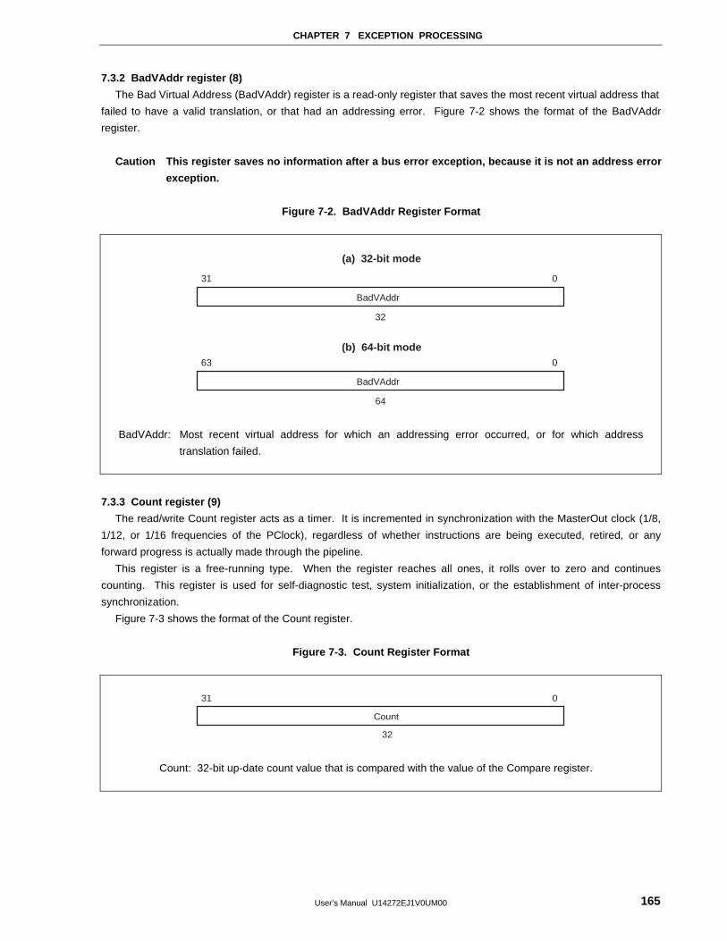
CHAPTER 7 EXCEPTION PROCESSING
User’s Manual U14272EJ1V0UM00 165
7.3.2 BadVAddr register (8)
The Bad Virtual Address (BadVAddr) register is a read-only register that saves the most recent virtual address that
failed to have a valid translation, or that had an addressing error. Figure 7-2 shows the format of the BadVAddr
register.
Caution This register saves no information after a bus error exception, because it is not an address error
exception.
Figure 7-2. BadVAddr Register Format
(a) 32-bit mode
32
031
BadVAddr
(b) 64-bit mode
64
063
BadVAddr
BadVAddr: Most recent virtual address for which an addressing error occurred, or for which address
translation failed.
7.3.3 Count register (9)
The read/write Count register acts as a timer. It is incremented in synchronization with the MasterOut clock (1/8,
1/12, or 1/16 frequencies of the PClock), regardless of whether instructions are being executed, retired, or any
forward progress is actually made through the pipeline.
This register is a free-running type. When the register reaches all ones, it rolls over to zero and continues
counting. This register is used for self-diagnostic test, system initialization, or the establishment of inter-process
synchronization.
Figure 7-3 shows the format of the Count register.
Figure 7-3. Count Register Format
031
Count
32
Count: 32-bit up-date count value that is compared with the value of the Compare register.
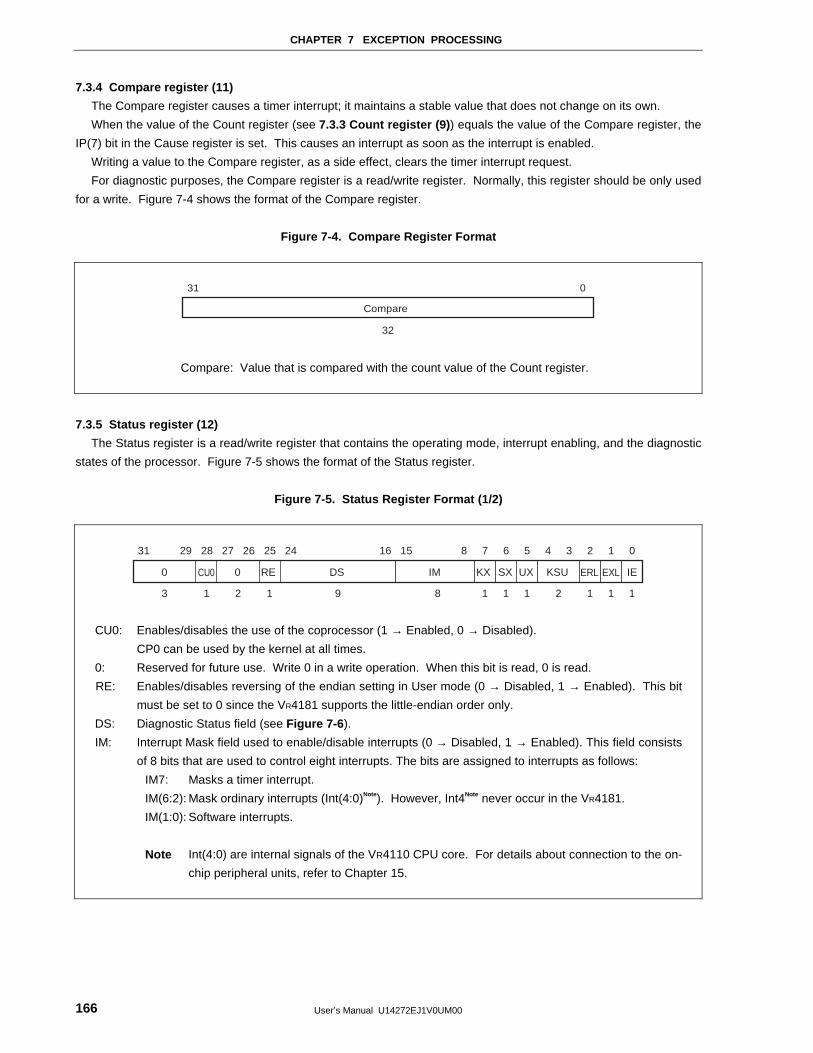
CHAPTER 7 EXCEPTION PROCESSING
User’s Manual U14272EJ1V0UM00166
7.3.4 Compare register (11)
The Compare register causes a timer interrupt; it maintains a stable value that does not change on its own.
When the value of the Count register (see 7.3.3 Count register (9) ) equals the value of the Compare register, the
IP(7) bit in the Cause register is set. This causes an interrupt as soon as the interrupt is enabled.
Writing a value to the Compare register, as a side effect, clears the timer interrupt request.
For diagnostic purposes, the Compare register is a read/write register. Normally, this register should be only used
for a write. Figure 7-4 shows the format of the Compare register.
Figure 7-4. Compare Register Format
32
031
Compare
Compare: Value that is compared with the count value of the Count register.
7.3.5 Status register (12)
The Status register is a read/write register that contains the operating mode, interrupt enabling, and the diagnostic
states of the processor. Figure 7-5 shows the format of the Status register.
Figure 7-5. Status Register Format (1/2)
29 28 27 26 25 24 16 15 8 7 6 5 3 2 1 031
0 CU0 0 RE DS IM UX KSU ERL
1213 9
IE
8 111211 1
KX SX EXL
4
CU0: Enables/disables the use of the coprocessor (1 → Enabled, 0 → Disabled).
CP0 can be used by the kernel at all times.
0: Reserved for future use. Write 0 in a write operation. When this bit is read, 0 is read.
RE: Enables/disables reversing of the endian setting in User mode (0 → Disabled, 1 → Enabled). This bit
must be set to 0 since the VR4181 supports the little-endian order only.
DS: Diagnostic Status field (see Figure 7-6 ).
IM: Interrupt Mask field used to enable/disable interrupts (0 → Disabled, 1 → Enabled). This field consists
of 8 bits that are used to control eight interrupts. The bits are assigned to interrupts as follows:
IM7: Masks a timer interrupt.
IM(6:2): Mask ordinary interrupts (Int(4:0)Note). However, Int4Note never occur in the VR4181.
IM(1:0): Software interrupts.
Note Int(4:0) are internal signals of the VR4110 CPU core. For details about connection to the on-
chip peripheral units, refer to Chapter 15.
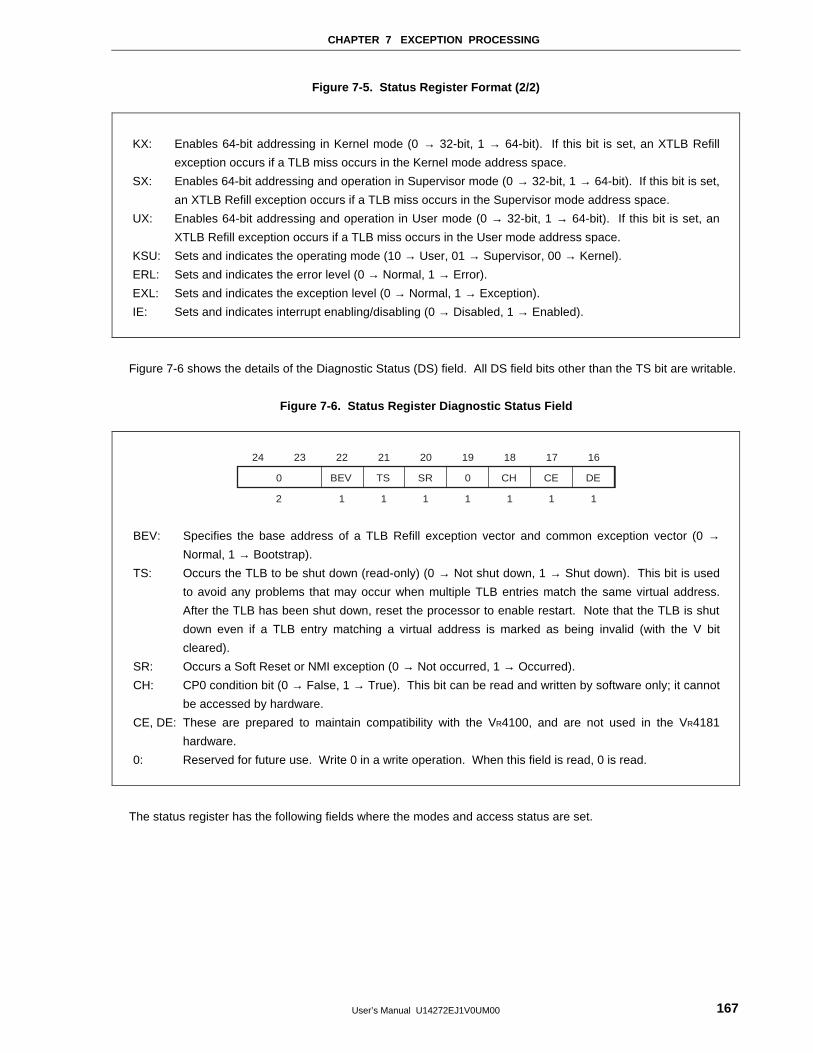
CHAPTER 7 EXCEPTION PROCESSING
User’s Manual U14272EJ1V0UM00 167
Figure 7-5. Status Register Format (2/2)
KX: Enables 64-bit addressing in Kernel mode (0 → 32-bit, 1 → 64-bit). If this bit is set, an XTLB Refill
exception occurs if a TLB miss occurs in the Kernel mode address space.
SX: Enables 64-bit addressing and operation in Supervisor mode (0 → 32-bit, 1 → 64-bit). If this bit is set,
an XTLB Refill exception occurs if a TLB miss occurs in the Supervisor mode address space.
UX: Enables 64-bit addressing and operation in User mode (0 → 32-bit, 1 → 64-bit). If this bit is set, an
XTLB Refill exception occurs if a TLB miss occurs in the User mode address space.
KSU: Sets and indicates the operating mode (10 → User, 01 → Supervisor, 00 → Kernel).
ERL: Sets and indicates the error level (0 → Normal, 1 → Error).
EXL: Sets and indicates the exception level (0 → Normal, 1 → Exception).
IE: Sets and indicates interrupt enabling/disabling (0 → Disabled, 1 → Enabled).
Figure 7-6 shows the details of the Diagnostic Status (DS) field. All DS field bits other than the TS bit are writable.
Figure 7-6. Status Register Diagnostic Status Field
161718192021222324
0 BEV TS SR 0 CH CE DE
11111112
BEV: Specifies the base address of a TLB Refill exception vector and common exception vector (0 →Normal, 1 → Bootstrap).
TS: Occurs the TLB to be shut down (read-only) (0 → Not shut down, 1 → Shut down). This bit is used
to avoid any problems that may occur when multiple TLB entries match the same virtual address.
After the TLB has been shut down, reset the processor to enable restart. Note that the TLB is shut
down even if a TLB entry matching a virtual address is marked as being invalid (with the V bit
cleared).
SR: Occurs a Soft Reset or NMI exception (0 → Not occurred, 1 → Occurred).
CH: CP0 condition bit (0 → False, 1 → True). This bit can be read and written by software only; it cannot
be accessed by hardware.
CE, DE: These are prepared to maintain compatibility with the VR4100, and are not used in the VR4181
hardware.
0: Reserved for future use. Write 0 in a write operation. When this field is read, 0 is read.
The status register has the following fields where the modes and access status are set.
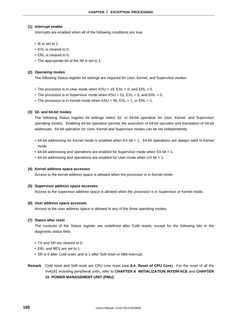
CHAPTER 7 EXCEPTION PROCESSING
User’s Manual U14272EJ1V0UM00168
(1) Interrupt enable
Interrupts are enabled when all of the following conditions are true:
• IE is set to 1.
• EXL is cleared to 0.
• ERL is cleared to 0.
• The appropriate bit of the IM is set to 1.
(2) Operating modes
The following Status register bit settings are required for User, Kernel, and Supervisor modes.
• The processor is in User mode when KSU = 10, EXL = 0, and ERL = 0.
• The processor is in Supervisor mode when KSU = 01, EXL = 0, and ERL = 0.
• The processor is in Kernel mode when KSU = 00, EXL = 1, or ERL = 1.
(3) 32- and 64-bit modes
The following Status register bit settings select 32- or 64-bit operation for User, Kernel, and Supervisor
operating modes. Enabling 64-bit operation permits the execution of 64-bit opcodes and translation of 64-bit
addresses. 64-bit operation for User, Kernel and Supervisor modes can be set independently.
• 64-bit addressing for Kernel mode is enabled when KX bit = 1. 64-bit operations are always valid in Kernel
mode.
• 64-bit addressing and operations are enabled for Supervisor mode when SX bit = 1.
• 64-bit addressing and operations are enabled for User mode when UX bit = 1.
(4) Kernel address space accesses
Access to the kernel address space is allowed when the processor is in Kernel mode.
(5) Supervisor address space accesses
Access to the supervisor address space is allowed when the processor is in Supervisor or Kernel mode.
(6) User address space accesses
Access to the user address space is allowed in any of the three operating modes.
(7) Status after reset
The contents of the Status register are undefined after Cold resets, except for the following bits in the
diagnostic status field.
• TS and SR are cleared to 0.
• ERL and BEV are set to 1.
• SR is 0 after Cold reset, and is 1 after Soft reset or NMI interrupt.
Remark Cold reset and Soft reset are CPU core reset (see 8.4 Reset of CPU Core ). For the reset of all the
VR4181 including peripheral units, refer to CHAPTER 8 INITIALIZATION INTERFACE and CHAPTER
15 POWER MANAGEMENT UNIT (PMU) .
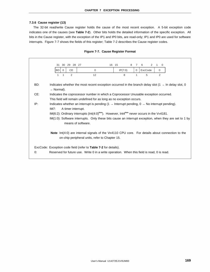
CHAPTER 7 EXCEPTION PROCESSING
User’s Manual U14272EJ1V0UM00 169
7.3.6 Cause register (13)
The 32-bit read/write Cause register holds the cause of the most recent exception. A 5-bit exception code
indicates one of the causes (see Table 7-2 ). Other bits holds the detailed information of the specific exception. All
bits in the Cause register, with the exception of the IP1 and IP0 bits, are read-only; IP1 and IP0 are used for software
interrupts. Figure 7-7 shows the fields of this register; Table 7-2 describes the Cause register codes.
Figure 7-7. Cause Register Format
827 16 15 67 2 1 0
12 8 1 5 2
31 30 29 28
BD 0 CE
211
0 IP(7:0) 0 ExcCode 0
BD: Indicates whether the most recent exception occurred in the branch delay slot (1 → In delay slot, 0
→ Normal).
CE: Indicates the coprocessor number in which a Coprocessor Unusable exception occurred.
This field will remain undefined for as long as no exception occurs.
IP: Indicates whether an interrupt is pending (1 → Interrupt pending, 0 → No interrupt pending).
IM7: A timer interrupt.
IM(6:2): Ordinary interrupts (Int(4:0)Note). However, Int4Note never occurs in the VR4181.
IM(1:0): Software interrupts. Only these bits cause an interrupt exception, when they are set to 1 by
means of software.
Note Int(4:0) are internal signals of the VR4110 CPU core. For details about connection to the
on-chip peripheral units, refer to Chapter 15.
ExcCode: Exception code field (refer to Table 7-2 for details).
0: Reserved for future use. Write 0 in a write operation. When this field is read, 0 is read.
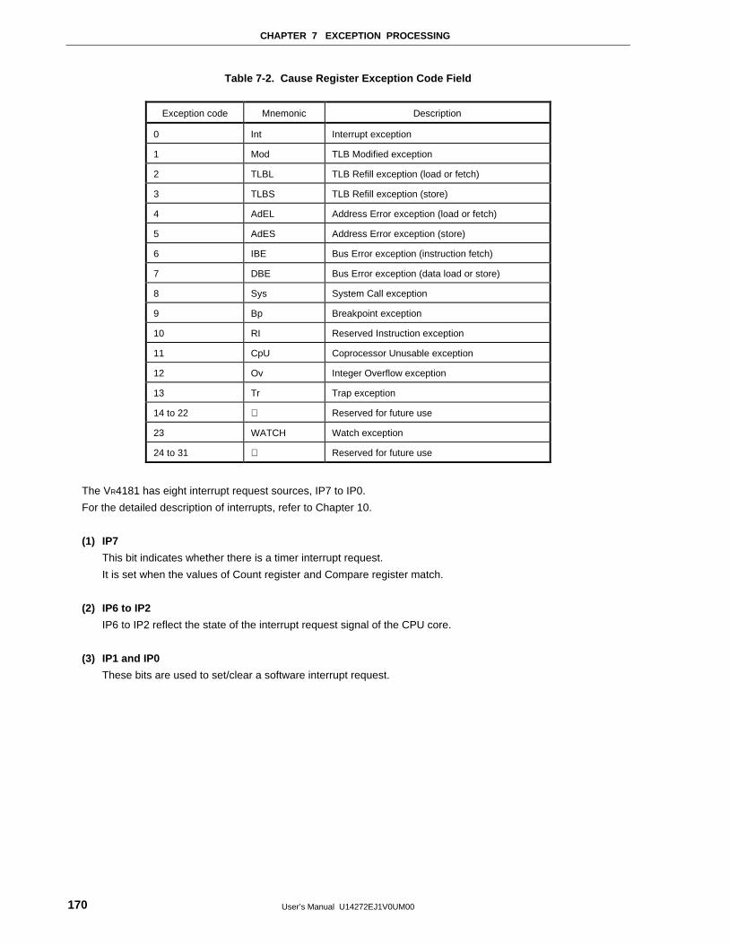
CHAPTER 7 EXCEPTION PROCESSING
User’s Manual U14272EJ1V0UM00170
Table 7-2. Cause Register Exception Code Field
Exception code Mnemonic Description
0 Int Interrupt exception
1 Mod TLB Modified exception
2 TLBL TLB Refill exception (load or fetch)
3 TLBS TLB Refill exception (store)
4 AdEL Address Error exception (load or fetch)
5 AdES Address Error exception (store)
6 IBE Bus Error exception (instruction fetch)
7 DBE Bus Error exception (data load or store)
8 Sys System Call exception
9 Bp Breakpoint exception
10 RI Reserved Instruction exception
11 CpU Coprocessor Unusable exception
12 Ov Integer Overflow exception
13 Tr Trap exception
14 to 22 Reserved for future use
23 WATCH Watch exception
24 to 31 Reserved for future use
The VR4181 has eight interrupt request sources, IP7 to IP0.
For the detailed description of interrupts, refer to Chapter 10.
(1) IP7
This bit indicates whether there is a timer interrupt request.
It is set when the values of Count register and Compare register match.
(2) IP6 to IP2
IP6 to IP2 reflect the state of the interrupt request signal of the CPU core.
(3) IP1 and IP0
These bits are used to set/clear a software interrupt request.
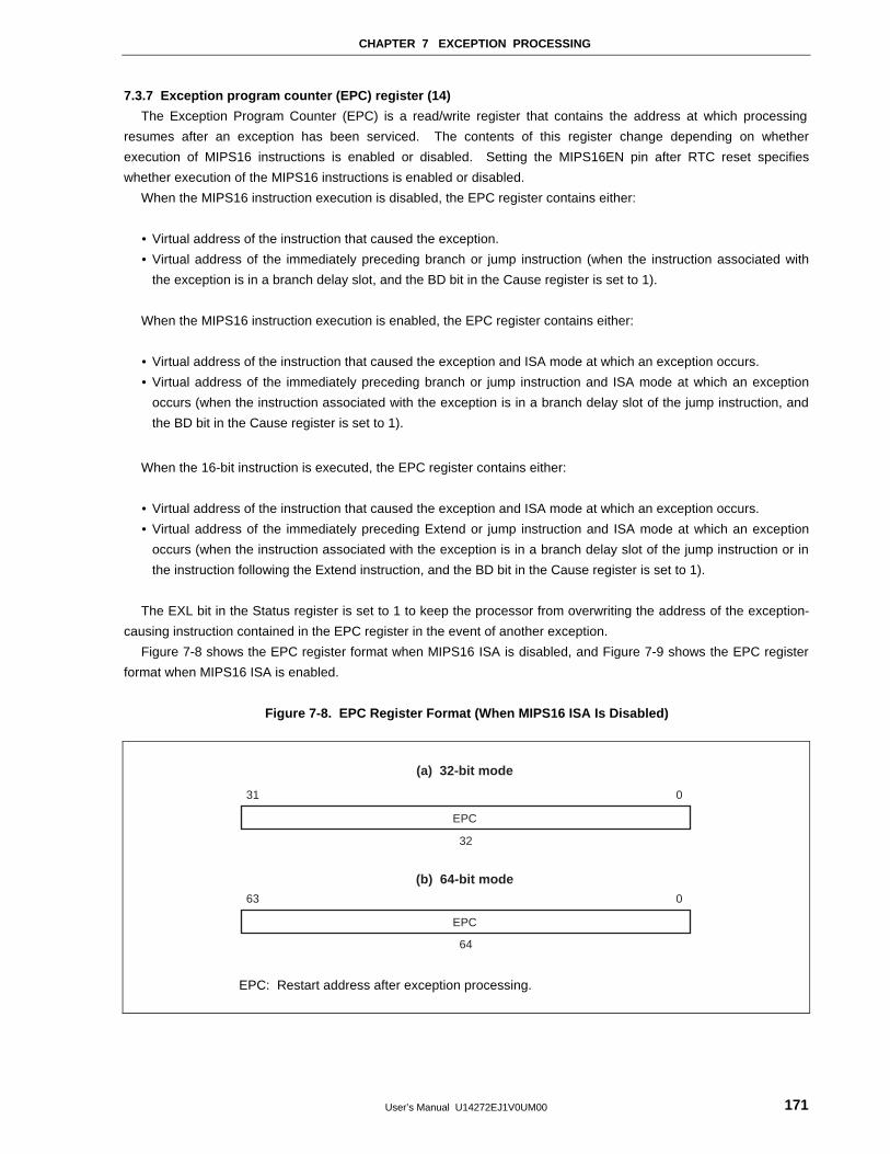
CHAPTER 7 EXCEPTION PROCESSING
User’s Manual U14272EJ1V0UM00 171
7.3.7 Exception program counter (EPC) register (14)
The Exception Program Counter (EPC) is a read/write register that contains the address at which processing
resumes after an exception has been serviced. The contents of this register change depending on whether
execution of MIPS16 instructions is enabled or disabled. Setting the MIPS16EN pin after RTC reset specifies
whether execution of the MIPS16 instructions is enabled or disabled.
When the MIPS16 instruction execution is disabled, the EPC register contains either:
• Virtual address of the instruction that caused the exception.
• Virtual address of the immediately preceding branch or jump instruction (when the instruction associated with
the exception is in a branch delay slot, and the BD bit in the Cause register is set to 1).
When the MIPS16 instruction execution is enabled, the EPC register contains either:
• Virtual address of the instruction that caused the exception and ISA mode at which an exception occurs.
• Virtual address of the immediately preceding branch or jump instruction and ISA mode at which an exception
occurs (when the instruction associated with the exception is in a branch delay slot of the jump instruction, and
the BD bit in the Cause register is set to 1).
When the 16-bit instruction is executed, the EPC register contains either:
• Virtual address of the instruction that caused the exception and ISA mode at which an exception occurs.
• Virtual address of the immediately preceding Extend or jump instruction and ISA mode at which an exception
occurs (when the instruction associated with the exception is in a branch delay slot of the jump instruction or in
the instruction following the Extend instruction, and the BD bit in the Cause register is set to 1).
The EXL bit in the Status register is set to 1 to keep the processor from overwriting the address of the exception-
causing instruction contained in the EPC register in the event of another exception.
Figure 7-8 shows the EPC register format when MIPS16 ISA is disabled, and Figure 7-9 shows the EPC register
format when MIPS16 ISA is enabled.
Figure 7-8. EPC Register Format (When MIPS16 ISA Is Disabled)
32
031
EPC
(a) 32-bit mode
(b) 64-bit mode
64
063
EPC
EPC: Restart address after exception processing.
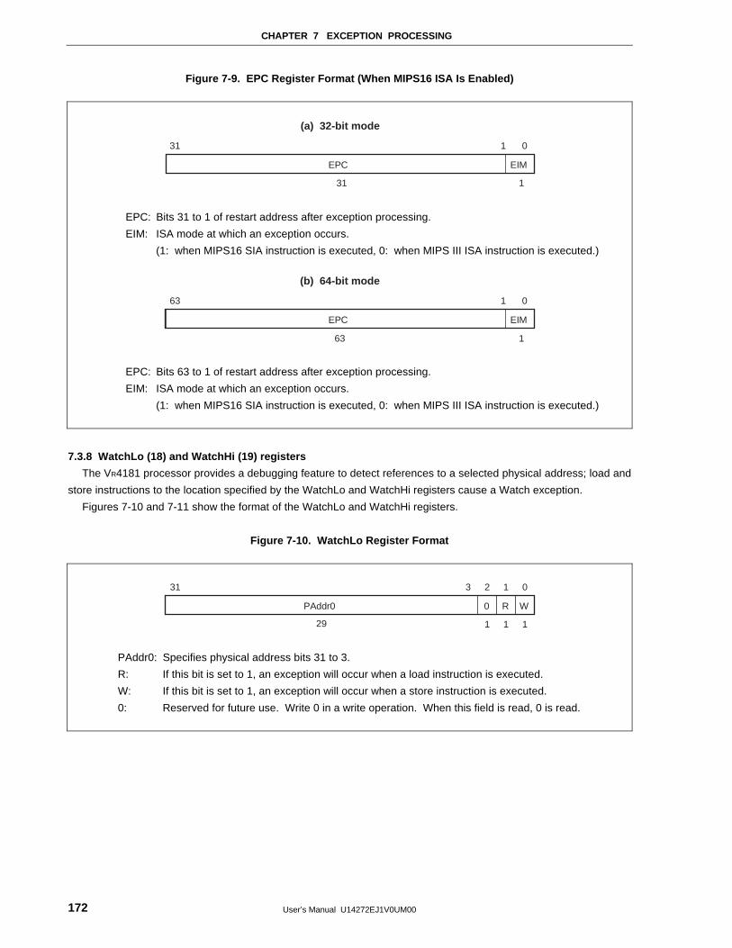
CHAPTER 7 EXCEPTION PROCESSING
User’s Manual U14272EJ1V0UM00172
Figure 7-9. EPC Register Format (When MIPS16 ISA Is Enabled)
1
(a) 32-bit mode
31
031
EPC EIM
1
EPC: Bits 31 to 1 of restart address after exception processing.
EIM: ISA mode at which an exception occurs.
(1: when MIPS16 SIA instruction is executed, 0: when MIPS III ISA instruction is executed.)
1
(b) 64-bit mode
63
063
EPC EIM
1
EPC: Bits 63 to 1 of restart address after exception processing.
EIM: ISA mode at which an exception occurs.
(1: when MIPS16 SIA instruction is executed, 0: when MIPS III ISA instruction is executed.)
7.3.8 WatchLo (18) and WatchHi (19) registers
The VR4181 processor provides a debugging feature to detect references to a selected physical address; load and
store instructions to the location specified by the WatchLo and WatchHi registers cause a Watch exception.
Figures 7-10 and 7-11 show the format of the WatchLo and WatchHi registers.
Figure 7-10. WatchLo Register Format
29
3 2 1 031
PAddr0 0 R W
1 1 1
PAddr0: Specifies physical address bits 31 to 3.
R: If this bit is set to 1, an exception will occur when a load instruction is executed.
W: If this bit is set to 1, an exception will occur when a store instruction is executed.
0: Reserved for future use. Write 0 in a write operation. When this field is read, 0 is read.
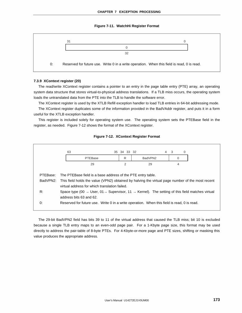
CHAPTER 7 EXCEPTION PROCESSING
User’s Manual U14272EJ1V0UM00 173
Figure 7-11. WatchHi Register Format
32
031
0
0: Reserved for future use. Write 0 in a write operation. When this field is read, 0 is read.
7.3.9 XContext register (20)
The read/write XContext register contains a pointer to an entry in the page table entry (PTE) array, an operating
system data structure that stores virtual-to-physical address translations. If a TLB miss occurs, the operating system
loads the untranslated data from the PTE into the TLB to handle the software error.
The XContext register is used by the XTLB Refill exception handler to load TLB entries in 64-bit addressing mode.
The XContext register duplicates some of the information provided in the BadVAddr register, and puts it in a form
useful for the XTLB exception handler.
This register is included solely for operating system use. The operating system sets the PTEBase field in the
register, as needed. Figure 7-12 shows the format of the XContext register.
Figure 7-12. XContext Register Format
32
42 2929
035 34 3363 4 3
PTEBase R BadVPN2 0
PTEBase: The PTEBase field is a base address of the PTE entry table.
BadVPN2: This field holds the value (VPN2) obtained by halving the virtual page number of the most recent
virtual address for which translation failed.
R: Space type (00 → User, 01→ Supervisor, 11 → Kernel). The setting of this field matches virtual
address bits 63 and 62.
0: Reserved for future use. Write 0 in a write operation. When this field is read, 0 is read.
The 29-bit BadVPN2 field has bits 39 to 11 of the virtual address that caused the TLB miss; bit 10 is excluded
because a single TLB entry maps to an even-odd page pair. For a 1-Kbyte page size, this format may be used
directly to address the pair-table of 8-byte PTEs. For 4-Kbyte-or-more page and PTE sizes, shifting or masking this
value produces the appropriate address.
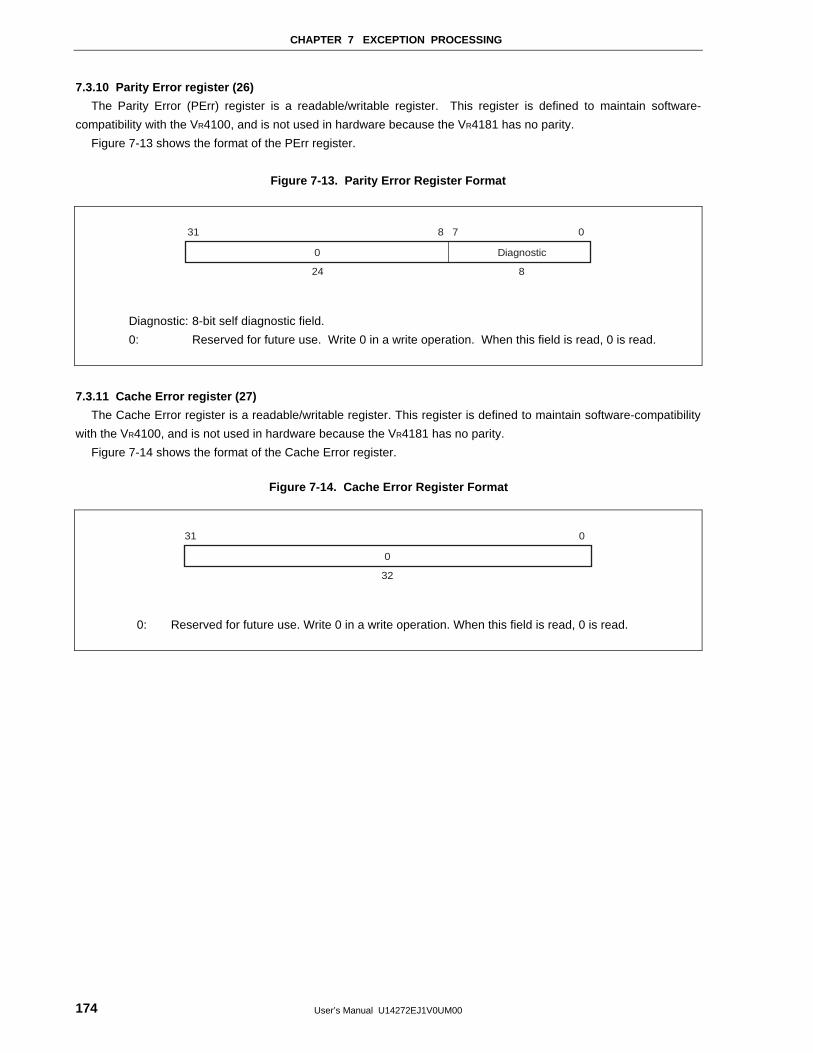
CHAPTER 7 EXCEPTION PROCESSING
User’s Manual U14272EJ1V0UM00174
7.3.10 Parity Error register (26)
The Parity Error (PErr) register is a readable/writable register. This register is defined to maintain software-
compatibility with the VR4100, and is not used in hardware because the VR4181 has no parity.
Figure 7-13 shows the format of the PErr register.
Figure 7-13. Parity Error Register Format
24
08 731
0 Diagnostic
8
Diagnostic: 8-bit self diagnostic field.
0: Reserved for future use. Write 0 in a write operation. When this field is read, 0 is read.
7.3.11 Cache Error register (27)
The Cache Error register is a readable/writable register. This register is defined to maintain software-compatibility
with the VR4100, and is not used in hardware because the VR4181 has no parity.
Figure 7-14 shows the format of the Cache Error register.
Figure 7-14. Cache Error Register Format
31 0
32
0
0: Reserved for future use. Write 0 in a write operation. When this field is read, 0 is read.
CHAPTER 7 EXCEPTION PROCESSING
User’s Manual U14272EJ1V0UM00 175
7.3.12 ErrorEPC register (30)
The Error Exception Program Counter (ErrorEPC) register is similar to the EPC register. It is used to store the
Program Counter value at which the Cache Error, Cold Reset, Soft Reset, or NMI exception has been serviced.
The read/write ErrorEPC register contains the virtual address at which instruction processing can resume after
servicing an error. The contents of this register change depending on whether execution of MIPS16 instructions is
enabled or disabled. Setting the MIPS16EN pin after RTC reset specifies whether the execution of MIPS16
instructions is enabled or disabled.
When the MIPS16 ISA is disabled, this address can be:
• Virtual address of the instruction that caused the exception.
• Virtual address of the immediately preceding branch or jump instruction, when the instruction associated with the
error exception is in a branch delay slot.
When the MIPS16 instruction execution is enabled during a 32-bit instruction execution, this address can be:
• Virtual address of the instruction that caused the exception and ISA mode at which an exception occurs.
• Virtual address of the immediately preceding branch or jump instruction and ISA mode at which an exception
occurs when the instruction associated with the exception is in a branch delay slot.
When the MIPS16 instruction execution is enabled during a 16-bit instruction execution, this address can be:
• Virtual address of the instruction that caused the exception and ISA mode at which an exception occurs.
• Virtual address of the immediately preceding jump instruction or Extend instruction and ISA mode at which an
exception occurs when the instruction associated with the exception is in a branch delay slot of the jump
instruction or is the instruction following the Extend instruction.
The contents of the ErrorEPC register do not change when the ERL bit of the Status register is set to 1. This
prevents the processor when other exceptions occur from overwriting the address of the instruction in this register
which causes an error exception.
There is no branch delay slot indication for the ErrorEPC register.
Figure 7-15 shows the format of the ErrorEPC register when the MIPS16ISA is disabled. Figure 7-16 shows the
format of the ErrorEPC register when the MIPS16ISA is enabled.
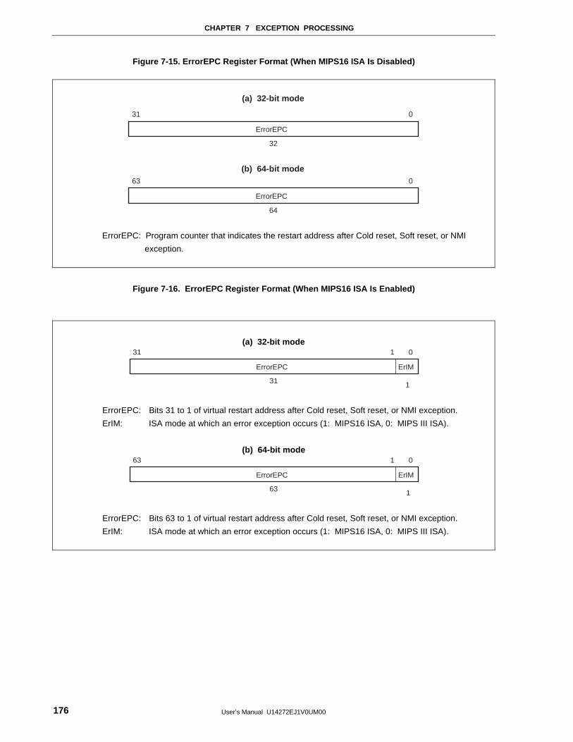
CHAPTER 7 EXCEPTION PROCESSING
User’s Manual U14272EJ1V0UM00176
Figure 7-15. ErrorEPC Register Format (When MIPS16 ISA Is Disabled)
(a) 32-bit mode
32
031
ErrorEPC
(b) 64-bit mode
64
063
ErrorEPC
ErrorEPC: Program counter that indicates the restart address after Cold reset, Soft reset, or NMI
exception.
Figure 7-16. ErrorEPC Register Format (When MIPS16 ISA Is Enabled)
(a) 32-bit mode1
31
031
ErrorEPC ErIM
1
ErrorEPC: Bits 31 to 1 of virtual restart address after Cold reset, Soft reset, or NMI exception.
ErIM: ISA mode at which an error exception occurs (1: MIPS16 ISA, 0: MIPS III ISA).
(b) 64-bit mode1
63
063
ErrorEPC ErIM
1
ErrorEPC: Bits 63 to 1 of virtual restart address after Cold reset, Soft reset, or NMI exception.
ErIM: ISA mode at which an error exception occurs (1: MIPS16 ISA, 0: MIPS III ISA).
CHAPTER 7 EXCEPTION PROCESSING
User’s Manual U14272EJ1V0UM00 177
7.4 Details of Exceptions
This section describes causes, processes, and services of the VR4181’s exceptions.
7.4.1 Exception types
This section gives sample exception handler operations for the following exception types:
• Cold Reset
• Soft Reset
• NMI
• Remaining processor exceptions
When the EXL and ERL bits in the Status register are 0, either User, Supervisor, or Kernel operating mode is
specified by the KSU bits in the Status register. When either the EXL or ERL bit is set to 1, the processor is in Kernel
mode.
When the processor takes an exception, the EXL bit is set to 1, meaning the system is in Kernel mode. After
saving the appropriate state, the exception handler typically resets the EXL bit back to 0. The exception handler sets
the EXL bit to 1 so that the saved state is not lost upon the occurrence of another exception while the saved state is
being restored.
Returning from an exception also resets the EXL bit to 0. For details, see CHAPTER 27 MIPS III INSTRUCTION
SET DETAILS .
7.4.2 Exception vector locations
The Cold Reset, Soft Reset, and NMI exceptions are always branched to the following reset exception vector
address (virtual). This address is in an uncached, unmapped space.
• 0xBFC0 0000 in 32-bit mode
• 0xFFFF FFFF BFC0 0000 in 64-bit mode
Addresses for the remaining exceptions are a combination of a vector offset and a base address.
64-/32-bit mode exception vectors and their offsets are shown below.
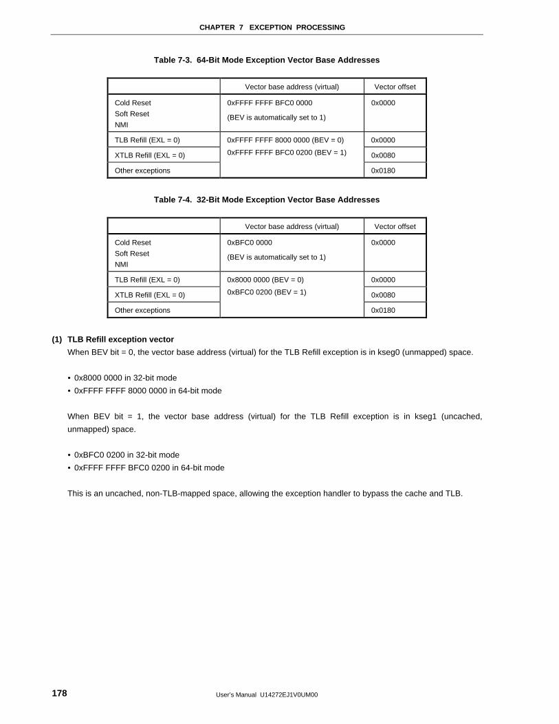
CHAPTER 7 EXCEPTION PROCESSING
User’s Manual U14272EJ1V0UM00178
Table 7-3. 64-Bit Mode Exception Vector Base Addresses
Vector base address (virtual) Vector offset
Cold Reset
Soft Reset
NMI
0xFFFF FFFF BFC0 0000
(BEV is automatically set to 1)
0x0000
TLB Refill (EXL = 0) 0xFFFF FFFF 8000 0000 (BEV = 0) 0x0000
XTLB Refill (EXL = 0) 0xFFFF FFFF BFC0 0200 (BEV = 1) 0x0080
Other exceptions 0x0180
Table 7-4. 32-Bit Mode Exception Vector Base Addresses
Vector base address (virtual) Vector offset
Cold Reset
Soft Reset
NMI
0xBFC0 0000
(BEV is automatically set to 1)
0x0000
TLB Refill (EXL = 0) 0x8000 0000 (BEV = 0) 0x0000
XTLB Refill (EXL = 0) 0xBFC0 0200 (BEV = 1) 0x0080
Other exceptions 0x0180
(1) TLB Refill exception vector
When BEV bit = 0, the vector base address (virtual) for the TLB Refill exception is in kseg0 (unmapped) space.
• 0x8000 0000 in 32-bit mode
• 0xFFFF FFFF 8000 0000 in 64-bit mode
When BEV bit = 1, the vector base address (virtual) for the TLB Refill exception is in kseg1 (uncached,
unmapped) space.
• 0xBFC0 0200 in 32-bit mode
• 0xFFFF FFFF BFC0 0200 in 64-bit mode
This is an uncached, non-TLB-mapped space, allowing the exception handler to bypass the cache and TLB.
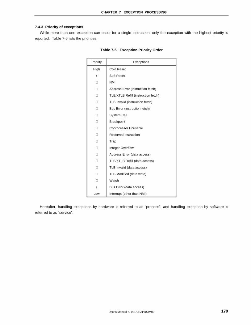
CHAPTER 7 EXCEPTION PROCESSING
User’s Manual U14272EJ1V0UM00 179
7.4.3 Priority of exceptions
While more than one exception can occur for a single instruction, only the exception with the highest priority is
reported. Table 7-5 lists the priorities.
Table 7-5. Exception Priority Order
Priority Exceptions
High
↑
↓
Low
Cold Reset
Soft Reset
NMI
Address Error (instruction fetch)
TLB/XTLB Refill (instruction fetch)
TLB Invalid (instruction fetch)
Bus Error (instruction fetch)
System Call
Breakpoint
Coprocessor Unusable
Reserved Instruction
Trap
Integer Overflow
Address Error (data access)
TLB/XTLB Refill (data access)
TLB Invalid (data access)
TLB Modified (data write)
Watch
Bus Error (data access)
Interrupt (other than NMI)
Hereafter, handling exceptions by hardware is referred to as “process”, and handling exception by software is
referred to as “service”.
CHAPTER 7 EXCEPTION PROCESSING
User’s Manual U14272EJ1V0UM00180
7.4.4 Cold Reset exception
Cause
The Cold Reset exception occurs when the ColdReset# signal (internal) is asserted and then deasserted. This
exception is not maskable. The Reset# signal (internal) must be asserted along with the ColdReset# signal (for
details, see Chapter 8).
Processing
The CPU provides a special interrupt vector for this exception:
• 0xBFC0 0000 (virtual) in 32-bit mode
• 0xFFFF FFFF BFC0 0000 (virtual) in 64-bit mode
The Cold Reset vector resides in unmapped and uncached CPU address space, so the hardware need not
initialize the TLB or the cache to process this exception. It also means the processor can fetch and execute
instructions while the caches and virtual memory are in an undefined state.
The contents of all registers in the CPU are undefined when this exception occurs, except for the following register
fields:
• When the MIPS16 instruction execution is disabled while the ERL of Status register is 0, the PC value at
which an exception occurs is set to the ErrorEPC register.
When the MIPS16 instruction execution is enabled while the ERL of Status register is 0, the PC value at
which an exception occurs is set to the ErrorEPC register and the ISA mode in which an exception occurs is
set to the least significant bit of the ErrorEPC register.
• TS and SR of the Status register are cleared to 0.
• ERL and BEV of the Status register are set to 1.
• The Random register is initialized to the value of its upper bound (31).
• The Wired register is initialized to 0.
• Bits 31 to 28 and bits 22 to 3 of the Config register are set to fixed values.
• All other bits are undefined.
Servicing
The Cold Reset exception is serviced by:
• Initializing all processor registers, coprocessor registers, TLB, caches, and the memory system
• Performing diagnostic tests
• Bootstrapping the operating system
CHAPTER 7 EXCEPTION PROCESSING
User’s Manual U14272EJ1V0UM00 181
7.4.5 Soft Reset exception
Cause
A Soft Reset (sometimes called Warm Reset) occurs when the ColdReset# signal remains deasserted while the
Reset# signal goes from assertion to deassertion (for details, see Chapter 8).
A Soft Reset immediately resets all state machines, and sets the SR bit of the Status register. Execution begins at
the reset vector when the reset is deasserted. This exception is not maskable.
Caution In the V R4181, a soft reset never occurs.
Processing
The CPU provides a special interrupt vector for this exception (same location as Cold Reset):
• 0xBFC0 0000 (virtual) in 32-bit mode
• 0xFFFF FFFF BFC0 0000 (virtual) in 64-bit mode
This vector is located within unmapped and uncached address space, so that the cache and TLB need not be
initialized to process this exception. The SR bit of the Status register is set to 1 to distinguish this exception from
a Cold Reset exception.
When this exception occurs, the contents of all registers are preserved except for the following registers:
• When the MIPS16 instruction execution is disabled, the PC value at which an exception occurs is set to the
ErrorEPC register.
When the MIPS16 instruction execution is enabled, the PC value at which an exception occurs is set to the
ErrorEPC register and the ISA mode in which an exception occurs is set to the least significant bit of the
ErrorEPC register.
• TS bit of the Status register is cleared to 0.
• ERL, SR, and BEV bits of the Status register are set to 1.
During a soft reset, access to the operating cache or system interface may be aborted. This means that the
contents of the cache and memory will be undefined if a Soft Reset occurs.
Servicing
The Soft Reset exception is serviced by:
• Preserving the current processor states for diagnostic tests
• Reinitializing the system in the same way as for a Cold Reset exception
CHAPTER 7 EXCEPTION PROCESSING
User’s Manual U14272EJ1V0UM00182
7.4.6 NMI exception
Cause
The Nonmaskable Interrupt (NMI) exception occurs when the NMI signal (internal) becomes active. This interrupt
is not maskable; it occurs regardless of the settings of the EXL, ERL, and the IE bits in the Status register (for
details, see Chapters 10 and 15).
Processing
The CPU provides a special interrupt vector for this exception:
• 0xBFC0 0000 (virtual) in 32-bit mode
• 0xFFFF FFFF BFC0 0000 (virtual) in 64-bit mode
This vector is located within unmapped and uncached address space so that the cache and TLB need not be
initialized to process an NMI interrupt. The SR bit of the Status register is set to 1 to distinguish this exception
from a Cold Reset exception.
Unlike Cold Reset and Soft Reset, but like other exceptions, NMI is taken only at instruction boundaries. The
states of the caches and memory system are preserved by this exception.
When this exception occurs, the contents of all registers are preserved except for the following registers:
• When the MIPS16 instruction execution is disabled, the PC value at which an exception occurs is set to the
ErrorEPC register.
When the MIPS16 instruction execution is enabled, the PC value at which an exception occurs is set to the
ErrorEPC register and the ISA mode in which an exception occurs is set to the least significant bit of the
ErrorEPC register.
• The TS bit of the Status register is cleared to 0.
• The ERL, SR, and BEV bits of the Status register are set to 1.
Servicing
The NMI exception is serviced by:
• Preserving the current processor states for diagnostic tests
• Reinitializing the system in the same way as for a Cold Reset exception
CHAPTER 7 EXCEPTION PROCESSING
User’s Manual U14272EJ1V0UM00 183
7.4.7 Address Error exception
Cause
The Address Error exception occurs when an attempt is made to execute one of the following. This exception is
not maskable.
• Execution of the LW, LWU, SW, or CACHE instruction for word data that is not located on a word boundary
• Execution of the LH, LHU, or SH instruction for half-word data that is not located on a half-word boundary
• Execution the LD or SD instruction for double-word data that is not located on a double-word boundary
• Referencing the kernel address space in User or Supervisor mode
• Referencing the supervisor space in User mode
• Referencing an address that does not exist in the kernel, user, or supervisor address space in 64-bit Kernel,
User, or Supervisor mode
• Branching to an address that was not located on a ward boundary when the MIPS16 instruction is disabled
• Branching to address whose least-significant 2 bits are 10 when the MIPS16 instruction is enabled
Processing
The common exception vector is used for this exception. The AdEL or AdES code in the Cause register is set. If
this exception has been caused by an instruction reference or load operation, AdEL is set. If it has been caused
by a store operation, AdES is set.
When this exception occurs, the BadVAddr register stores the virtual address that was not properly aligned or was
referenced in protected address space. The contents of the VPN field of the Context and EntryHi registers are
undefined, as are the contents of the EntryLo register.
When the MIPS16 instruction is disabled, the EPC register contains the address of the instruction that caused the
exception. However, if this instruction is in a branch delay slot, the EPC register contains the address of the
preceding jump or branch instruction, and the BD bit of the Cause register is set to 1.
When the MIPS16 instruction is enabled, the EPC register contains the address of the instruction that caused the
exception, and the least significant bit stores the ISA mode in which an exception occurs. However, if this
instruction is in a branch delay slot or is the instruction following the Extend instruction, the EPC register contains
the address of the preceding jump or Extend instruction, and the BD bit of the Cause register is set to 1.
Servicing
The kernel reports the UNIXTM SIGSEGV (segmentation violation) signal to the current process, and this exception
is usually fatal.
CHAPTER 7 EXCEPTION PROCESSING
User’s Manual U14272EJ1V0UM00184
7.4.8 TLB exceptions
Three types of TLB exceptions can occur:
• TLB Refill exception occurs when there is no TLB entry that matches a referenced address.
• A TLB Invalid exception occurs when a TLB entry that matches a referenced virtual address is marked as
being invalid (with the V bit set to 0).
• The TLB Modified exception occurs when a TLB entry that matches a virtual address referenced by the store
instruction is marked as being valid (with the V bit set to 1).
The following three sections describe these TLB exceptions.
(1) TLB Refill exception (32-bit space mode)/XTLB Refill exception (64-bit space mode)
Cause
The TLB Refill exception occurs when there is no TLB entry to match a reference to a mapped address space.
This exception is not maskable.
Processing
There are two special exception vectors for this exception; one for references to 32-bit address spaces, and one
for references to 64-bit address spaces. The UX, SX, and KX bits of the Status register determine whether the
user, supervisor or kernel address spaces referenced are 32-bit or 64-bit spaces. When the EXL bit of the Status
register is set to 0, either of these two special vectors is referenced. When the EXL bit is set to 1, the common
exception vector is referenced.
This exception sets the TLBL or TLBS code in the ExcCode field of the Cause register. If this exception has been
caused by an instruction reference or load operation, TLBL is set. If it has been caused by a store operation,
TLBS is set.
When this exception occurs, the BadVAddr, Context, XContext and EntryHi registers hold the virtual address that
failed address translation. The EntryHi register also contains the ASID from which the translation fault occurred.
The Random register normally contains a valid location in which to place the replacement TLB entry. The
contents of the EntryLo register are undefined.
When the MIPS16 instruction is disabled, the EPC register contains the address of the instruction that caused the
exception. However, if this instruction is in a branch delay slot, the EPC register contains the address of the
preceding jump or branch instruction, and the BD bit of the Cause register is set to 1.
When the MIPS16 instruction is enabled, the EPC register contains the address of the instruction that caused the
exception, and the least significant bit stores the ISA mode in which an exception occurs. However, if this
instruction is in a branch delay slot or is the instruction following the Extend instruction, the EPC register contains
the address of the preceding jump or Extend instruction, and the BD bit of the Cause register is set to 1.
CHAPTER 7 EXCEPTION PROCESSING
User’s Manual U14272EJ1V0UM00 185
Servicing
To service this exception, the contents of the Context or XContext register are used as a virtual address to fetch
memory words containing the physical page frame and access control bits for a pair of TLB entries. The memory
word is written into the TLB entry by using the EntryLo0, EntryLo1, or EntryHi register.
It is possible that the physical page frame and access control bits are placed in a page where the virtual address
is not resident in the TLB. This condition is processed by allowing a TLB Refill exception in the TLB Refill
exception handler. In this case, the common exception vector is used because the EXL bit of the Status register
is set to 1.
(2) TLB Invalid exception
Cause
The TLB Invalid exception occurs when the TLB entry that matches with the virtual address to be referenced is
invalid (the V bit is set to 0). This exception is not maskable.
Processing
The common exception vector is used for this exception. The TLBL or TLBS code in the ExcCode field of the
Cause register is set. If this exception has been caused by an instruction reference or load operation, TLBL is set.
If it has been caused by a store operation, TLBS is set.
When this exception occurs, the BadVAddr, Context, Xcontext, and EntryHi registers contain the virtual address
that failed address translation. The EntryHi register also contains the ASID from which the translation fault
occurred. The Random register normally stores a valid location in which to place the replacement TLB entry. The
contents of the EntryLo register are undefined.
When the MIPS16 instruction is disabled, the EPC register contains the address of the instruction that caused the
exception. However, if this instruction is in a branch delay slot, the EPC register contains the address of the
preceding jump or branch instruction, and the BD bit of the Cause register is set to 1.
When the MIPS16 instruction is enabled, the EPC register contains the address of the instruction that caused the
exception, and the least significant bit stores the ISA mode in which an exception occurs. However, if this
instruction is in a branch delay slot or is the instruction following the Extend instruction, the EPC register contains
the address of the preceding jump or Extend instruction, and the BD bit of the Cause register is set to 1.
Servicing
Usually, the V bit of a TLB entry is cleared in the following cases:
• When a virtual address does not exist
• When the virtual address exists, but is not in main memory (a page fault)
• When a trap is required on any reference to the page (for example, to maintain a reference bit)
After servicing the cause of a TLB Invalid exception, the TLB entry is located with a TLBP (TLB Probe) instruction,
and replaced by an entry with its Valid bit set to 1.
CHAPTER 7 EXCEPTION PROCESSING
User’s Manual U14272EJ1V0UM00186
(3) TLB Modified exception
Cause
The TLB Modified exception occurs when the TLB entry that matches with the virtual address referenced by the
store instruction is valid (bit V is 1) but is not writable (bit D is 0). This exception is not maskable.
Processing
The common exception vector is used for this exception, and the Mod code in the ExcCode field of the Cause
register is set.
When this exception occurs, the BadVAddr, Context, Xcontext, and EntryHi registers contain the virtual address
that failed address translation. The EntryHi register also contains the ASID from which the translation fault
occurred. The contents of the EntryLo register are undefined.
When the MIPS16 instruction is disabled, the EPC register contains the address of the instruction that caused the
exception. However, if this instruction is in a branch delay slot, the EPC register contains the address of the
preceding jump or branch instruction, and the BD bit of the Cause register is set to 1.
When the MIPS16 instruction is enabled, the EPC register contains the address of the instruction that caused the
exception, and the least significant bit stores the ISA mode in which an exception occurs. However, if this
instruction is in a branch delay slot or is the instruction following the Extend instruction, the EPC register contains
the address of the preceding jump or Extend instruction, and the BD bit of the Cause register is set to 1.
Servicing
The kernel uses the failed virtual address or virtual page number to identify the corresponding access control bits.
The page identified may or may not permit write accesses; if writes are not permitted, a write protection violation
occurs.
If write accesses are permitted, the page frame is marked dirty (/writable) by the kernel in its own data structures.
The TLBP instruction places the index of the TLB entry that must be altered into the Index register. The word data
containing the physical page frame and access control bits (with the D bit set to 1) is loaded to the EntryLo
register, and the contents of the EntryHi and EntryLo registers are written into the TLB.
CHAPTER 7 EXCEPTION PROCESSING
User’s Manual U14272EJ1V0UM00 187
7.4.9 Bus Error exception
Cause
A Bus Error exception is raised by board-level circuitry for events such as bus time-out, local bus parity errors, and
invalid physical memory addresses or access types. This exception is not maskable.
A Bus Error exception occurs only when a cache miss refill, uncached reference, or unbuffered write occurs
synchronously.
Processing
The common interrupt vector is used for a Bus Error exception. The IBE or DBE code in the ExcCode field of the
Cause register is set, signifying whether the instruction caused the exception by an instruction reference, load
operation, or store operation.
When the MIPS16 instruction is disabled, the EPC register contains the address of the instruction that caused the
exception. However, if this instruction is in a branch delay slot, the EPC register contains the address of the
preceding jump or branch instruction, and the BD bit of the Cause register is set to 1.
When the MIPS16 instruction is enabled, the EPC register contains the address of the instruction that caused the
exception, and the least significant bit stores the ISA mode in which an exception occurs. However, if this
instruction is in a branch delay slot or is the instruction following the Extend instruction, the EPC register contains
the address of the preceding jump or Extend instruction, and the BD bit of the Cause register is set to 1.
Servicing
The physical address at which the fault occurred can be computed from information available in the System
Control Coprocessor (CP0) registers.
• If the IBE code in the Cause register is set (indicating an instruction fetch), the virtual address is contained in
the EPC register (or 4 + the contents of the EPC register if the BD bit of the Cause register is set to 1).
• If the DBE code is set (indicating a load or store), the virtual address of the instruction that caused the
exception is saved to the EPC register.
The virtual address of the load and store instruction can then be obtained by interpreting the instruction. The
physical address can be obtained by using the TLBP instruction and reading the EntryLo register to compute the
physical page number.
At the time of this exception, the kernel reports the UNIX SIGBUS (bus error) signal to the current process, but the
exception is usually fatal.
CHAPTER 7 EXCEPTION PROCESSING
User’s Manual U14272EJ1V0UM00188
7.4.10 System Call exception
Cause
A System Call exception occurs during an attempt to execute the SYSCALL instruction. This exception is not
maskable.
Processing
The common exception vector is used for this exception, and the Sys code in the ExcCode field of the Cause
register is set.
The EPC register contains the address of the SYSCALL instruction unless it is in a branch delay slot, in which
case the EPC register contains the address of the preceding branch instruction.
If the SYSCALL instruction is in a branch delay slot, the BD bit of the Status register is set to 1; otherwise this bit
is cleared.
Servicing
When this exception occurs, control is transferred to the applicable system routine.
To resume execution, the EPC register must be altered so that the SYSCALL instruction does not re-execute; this
is accomplished by adding a value of 4 to the EPC register before returning.
If a SYSCALL instruction is in a branch delay slot, interpretation of the branch instruction is required to resume
execution.
CHAPTER 7 EXCEPTION PROCESSING
User’s Manual U14272EJ1V0UM00 189
7.4.11 Breakpoint exception
Cause
A Breakpoint exception occurs when an attempt is made to execute the BREAK instruction. This exception is not
maskable.
Processing
The common exception vector is used for this exception, and the BP code in the ExcCode field of the Cause
register is set.
When the MIPS16 instruction is disabled, the EPC register contains the address of the instruction that caused the
exception. However, if this instruction is in a branch delay slot, the EPC register contains the address of the
preceding jump or branch instruction, and the BD bit of the Cause register is set to 1.
When the MIPS16 instruction is enabled, the EPC register contains the address of the instruction that caused the
exception, and the least significant bit stores the ISA mode in which an exception occurs. However, if this
instruction is in a branch delay slot or is the instruction following the Extend instruction, the EPC register contains
the address of the preceding jump or Extend instruction, and the BD bit of the Cause register is set to 1.
Servicing
When the Breakpoint exception occurs, control is transferred to the applicable system routine. Additional
distinctions can be made by analyzing the unused bits of the BREAK instruction (bits 25 to 6), and loading the
contents of the instruction whose address the EPC register contains. A value of 4 must be added to the contents
of the EPC register to locate the instruction if it resides in a branch delay slot.
To resume execution, the EPC register must be altered so that the BREAK instruction does not re-execute; this is
accomplished by adding a value of 4 to the EPC register before returning.
When a Breakpoint exception occurs while executing the MIPS16 instruction, a valve of 2 should be added to the
EPC register before returning.
If a BREAK instruction is in a branch delay slot, interpretation (decoding) of the branch instruction is required to
resume execution.
CHAPTER 7 EXCEPTION PROCESSING
User’s Manual U14272EJ1V0UM00190
7.4.12 Coprocessor Unusable exception
Cause
The Coprocessor Unusable exception occurs when an attempt is made to execute a coprocessor instruction for
either:
• a corresponding coprocessor unit that has not been marked usable (Status register bit, CU[0] = 0), or
• CP0 instructions, when the unit has not been marked usable (Status register bit, CU[0] = 0) and the process
executes in User or Supervisor mode.
This exception is not maskable.
Processing
The common exception vector is used for this exception, and the CPU code in the ExcCode field of the Cause
register is set. The CE bit of the Cause register indicates which of the four coprocessors was referenced.
When the MIPS16 instruction is disabled, the EPC register contains the address of the instruction that caused the
exception. However, if this instruction is in a branch delay slot, the EPC register contains the address of the
preceding jump or branch instruction, and the BD bit of the Cause register is set to 1.
When the MIPS16 instruction is enabled, the EPC register contains the address of the instruction that caused the
exception, and the least significant bit stores the ISA mode in which an exception occurs. However, if this
instruction is in a branch delay slot or is the instruction following the Extend instruction, the EPC register contains
the address of the preceding jump or Extend instruction, and the BD bit of the Cause register is set to 1.
Servicing
The coprocessor unit to which an attempted reference was made is identified by the CE bit of the Cause register.
One of the following processing is performed by the handler:
• If the process is entitled access to the coprocessor, the coprocessor is marked usable and the corresponding
state is restored to the coprocessor.
• If the process is entitled access to the coprocessor, but the coprocessor does not exist or has failed,
interpretation of the coprocessor instruction is possible.
• If the BD bit in the Cause register is set to 1, the branch instruction must be interpreted; then the coprocessor
instruction can be emulated and execution resumed with the EPC register advanced past the coprocessor
instruction.
• If the process is not entitled access to the coprocessor, the kernel reports UNIX SIGILL/ILL_PRIVIN_FAULT
(illegal instruction/privileged instruction fault) signal to the current process, and this exception is fatal.
CHAPTER 7 EXCEPTION PROCESSING
User’s Manual U14272EJ1V0UM00 191
7.4.13 Reserved Instruction exception
Cause
The Reserved Instruction exception occurs when an attempt is made to execute one of the following instructions:
• Instruction with an undefined major opcode (bits 31 to 26)
• SPECIAL instruction with an undefined minor opcode (bits 5 to 0)
• REGIMM instruction with an undefined minor opcode (bits 20 to 16)
• 64-bit instructions in 32-bit User or Supervisor mode
• RR instruction with an undefined minor op code (bits 4 to 0) when executing the MIPS16 instruction
• I8 instruction with an undefined minor op code (bits 10 to 8) when executing the MIPS16 instruction
64-bit operations are always valid in Kernel mode regardless of the value of the KX bit in the Status register. This
exception is not maskable.
Processing
The common exception vector is used for this exception, and the RI code in the ExcCode field of the Cause
register is set.
When the MIPS16 instruction is disabled, the EPC register contains the address of the instruction that caused the
exception. However, if this instruction is in a branch delay slot, the EPC register contains the address of the
preceding jump or branch instruction, and the BD bit of the Cause register is set to 1.
When the MIPS16 instruction is enabled, the EPC register contains the address of the instruction that caused the
exception, and the least significant bit stores the ISA mode in which an exception occurs. However, if this
instruction is in a branch delay slot or is the instruction following the Extend instruction, the EPC register contains
the address of the preceding jump or Extend instruction, and the BD bit of the Cause register is set to 1.
Servicing
All currently defined MIPS ISA instructions can be executed. The process executing at the time of this exception
is handled by a UNIX SIGILL/ILL_RESOP_FAULT (illegal instruction/reserved operand fault) signal. This error is
usually fatal.
CHAPTER 7 EXCEPTION PROCESSING
User’s Manual U14272EJ1V0UM00192
7.4.14 Trap exception
Cause
The Trap exception occurs when a TGE, TGEU, TLT, TLTU, TEQ, TNE, TGEI, TGEUI, TLTI, TLTUI, TEQI, or
TNEI instruction results in a TRUE condition. This exception is not maskable.
Processing
The common exception vector is used for this exception, and the Tr code in the ExcCode field of the Cause
register is set.
The EPC register contains the address of the trap instruction causing the exception unless the instruction is in a
branch delay slot, in which case the EPC register contains the address of the preceding branch instruction and the
BD bit of the Cause register is set to 1.
Servicing
At the time of a Trap exception, the kernel reports the UNIX SIGFPE/FPE_INTOVF_TRAP (floating-point
exception/integer overflow) signal to the current process, but the exception is usually fatal.
7.4.15 Integer Overflow exception
Cause
An Integer Overflow exception occurs when an ADD, ADDI, SUB, DADD, DADDI, or DSUB instruction results in a
2’s complement overflow. This exception is not maskable.
Processing
The common exception vector is used for this exception, and the Ov code in the ExcCode field of the Cause
register is set.
The EPC register contains the address of the instruction that caused the exception unless the instruction is in a
branch delay slot, in which case the EPC register contains the address of the preceding branch instruction and the
BD bit of the Cause register is set to 1.
Servicing
At the time of the exception, the kernel reports the UNIX SIGFPE/FPE_INTOVF_TRAP (floating-point
exception/integer overflow) signal to the current process, and this exception is usually fatal.
CHAPTER 7 EXCEPTION PROCESSING
User’s Manual U14272EJ1V0UM00 193
7.4.16 Watch exception
Cause
A Watch exception occurs when a load or store instruction references the physical address specified by the
WatchLo/WatchHi registers. The WatchLo/WatchHi registers specify whether a load or store or both could have
initiated this exception.
• When the R bit of the WatchLo register is set to 1: Load instruction
• When the W bit of the WatchLo register is set to 1: Store instruction
• When both the R bit and W bit of the WatchLo register are set to 1: Load instruction or store instruction
The CACHE instruction never causes a Watch exception.
The Watch exception is postponed while the EXL bit in the Status register is set to 1, and Watch exception is only
maskable by setting the EXL bit in the Status register to 1.
Processing
The common exception vector is used for this exception, and the WATCH code in the ExcCode field of the Cause
register is set.
When the MIPS16 instruction is disabled, the EPC register contains the address of the instruction that caused the
exception. However, if this instruction is in a branch delay slot, the EPC register contains the address of the
preceding jump or branch instruction, and the BD bit of the Cause register is set to 1.
When the MIPS16 instruction is enabled, the EPC register contains the address of the instruction that caused the
exception, and the least significant bit stores the ISA mode in which an exception occurs. However, if this
instruction is in a branch delay slot or is the instruction following the Extend instruction, the EPC register contains
the address of the preceding jump or Extend instruction, and the BD bit of the Cause register is set to 1.
Servicing
The Watch exception is a debugging aid; typically the exception handler transfers control to a debugger, allowing
the user to examine the situation. To continue, once the Watch exception must be disabled to execute the faulting
instruction. The Watch exception must then be reenabled. The faulting instruction can be executed either by the
debugger or by setting breakpoints.
CHAPTER 7 EXCEPTION PROCESSING
User’s Manual U14272EJ1V0UM00194
7.4.17 Interrupt exception
Cause
The Interrupt exception occurs when one of the eight interrupt conditionsNote is asserted. In the VR4181, interrupt
requests from internal peripheral units first enter the ICU and are then notified to the CPU core via one of four
interrupt sources (Int [3:0]) or NMI.
Each of the eight interrupts can be masked by clearing the corresponding bit in the IM field of the Status register,
and all of the eight interrupts can be masked at once by clearing the IE bit of the Status register or setting the
EXL/ERL bit.
Note They are 1 timer interrupt, 5 ordinary interrupts, and 2 software interrupts.
Of the five ordinary interrupts, Int4 is never asserted active.
Processing
The common exception vector is used for this exception, and the Int code in the ExcCode field of the Cause
register is set.
The IP field of the Cause register indicates current interrupt requests. It is possible that more than one of the bits
can be simultaneously set (or cleared) if the interrupt request signal is asserted and then deasserted before this
register is read.
When the MIPS16 instruction is disabled, the EPC register contains the address of the instruction that caused the
exception. However, if this instruction is in a branch delay slot, the EPC register contains the address of the
preceding jump or branch instruction, and the BD bit of the Cause register is set to 1.
When the MIPS16 instruction is enabled, the EPC register contains the address of the instruction that caused the
exception, and the least significant bit stores the ISA mode in which an exception occurs. However, if this
instruction is in a branch delay slot or is the instruction following the Extend instruction, the EPC register contains
the address of the preceding jump or Extend instruction, and the BD bit of the Cause register is set to 1.
Servicing
If the interrupt is caused by one of the two software-generated exceptions (SW0 or SW1), the interrupt condition is
cleared by setting the corresponding Cause register bit to 0.
If the interrupt is caused by hardware, the interrupt condition is cleared by deactivating the corresponding interrupt
request signal.
CHAPTER 7 EXCEPTION PROCESSING
User’s Manual U14272EJ1V0UM00 195
7.5 Exception Processing and Servicing Flowcharts
The remainder of this chapter contains flowcharts for the following exceptions and guidelines for their handlers:
• Common exceptions and a guideline to their exception handler
• TLB/XTLB Refill exception and a guideline to their exception handler
• Cold Reset, Soft Reset and NMI exceptions, and a guideline to their handler.
Generally speaking, the exceptions are "processed” by hardware (HW); the exceptions are then “serviced” by
software (SW).
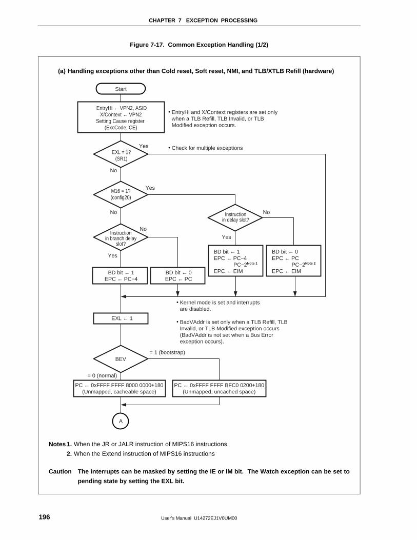
CHAPTER 7 EXCEPTION PROCESSING
User’s Manual U14272EJ1V0UM00196
Figure 7-17. Common Exception Handling (1/2)
(a) Handling exceptions other than Cold reset, Soft reset, NMI, and TLB/XTLB Refill (hardware)
EXL ← 1
= 0 (normal)
= 1 (bootstrap)
EntryHi ← VPN2, ASIDX/Context ← VPN2
Setting Cause register (ExcCode, CE)
BD bit ← 1EPC ← PC−4
BD bit ← 0EPC ← PC
YesEXL = 1?
(SR1)
No
No
Yes
BEV
M16 = 1?(config20)
Instructionin branch delay
slot?
PC ← 0xFFFF FFFF 8000 0000+180(Unmapped, cacheable space)
PC ← 0xFFFF FFFF BFC0 0200+180(Unmapped, uncached space)
No
BD bit ← 1EPC ← PC−4 PC−2Note 1
EPC ← EIM
BD bit ← 0EPC ← PC PC−2Note 2
EPC ← EIM
No
Yes
Yes
EntryHi and X/Context registers are set onlywhen a TLB Refill, TLB Invalid, or TLBModified exception occurs.
Kernel mode is set and interruptsare disabled.
BadVAddr is set only when a TLB Refill, TLBInvalid, or TLB Modified exception occurs(BadVAddr is not set when a Bus Errorexception occurs).
Check for multiple exceptions
Start
Instructionin delay slot?
A
Notes 1. When the JR or JALR instruction of MIPS16 instructions
2. When the Extend instruction of MIPS16 instructions
Caution The interrupts can be masked by setting the IE or IM bit. The Watch exception can be set to
pending state by setting the EXL bit.
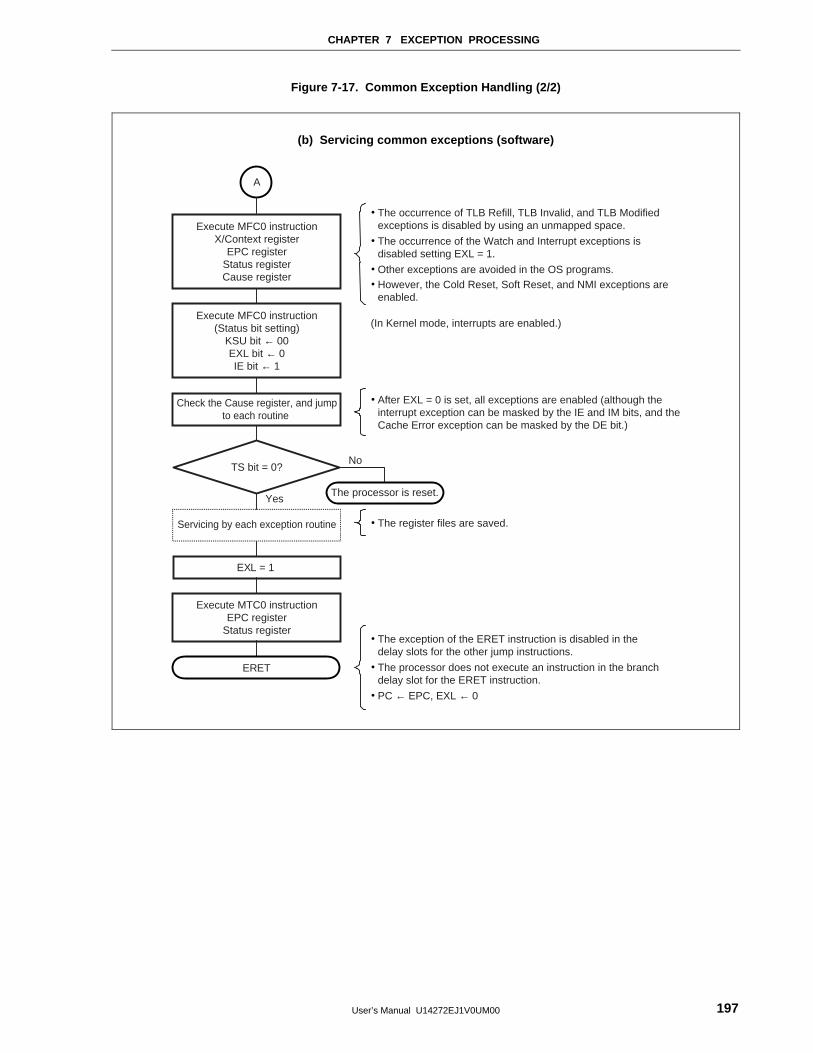
CHAPTER 7 EXCEPTION PROCESSING
User’s Manual U14272EJ1V0UM00 197
Figure 7-17. Common Exception Handling (2/2)
(b) Servicing common exceptions (software)
Execute MFC0 instructionX/Context register
EPC registerStatus registerCause register
Execute MFC0 instruction(Status bit setting)
KSU bit ← 00EXL bit ← 0IE bit ← 1
Execute MTC0 instructionEPC register
Status register
Servicing by each exception routine
Check the Cause register, and jumpto each routine
Yes
No
EXL = 1
The occurrence of TLB Refill, TLB Invalid, and TLB Modifiedexceptions is disabled by using an unmapped space.
The occurrence of the Watch and Interrupt exceptions isdisabled setting EXL = 1.
Other exceptions are avoided in the OS programs.
The exception of the ERET instruction is disabled in thedelay slots for the other jump instructions.
The processor does not execute an instruction in the branchdelay slot for the ERET instruction.
PC ← EPC, EXL ← 0
However, the Cold Reset, Soft Reset, and NMI exceptions areenabled.
(In Kernel mode, interrupts are enabled.)
After EXL = 0 is set, all exceptions are enabled (although theinterrupt exception can be masked by the IE and IM bits, and theCache Error exception can be masked by the DE bit.)
The register files are saved.
TS bit = 0?
ERET
The processor is reset.
A
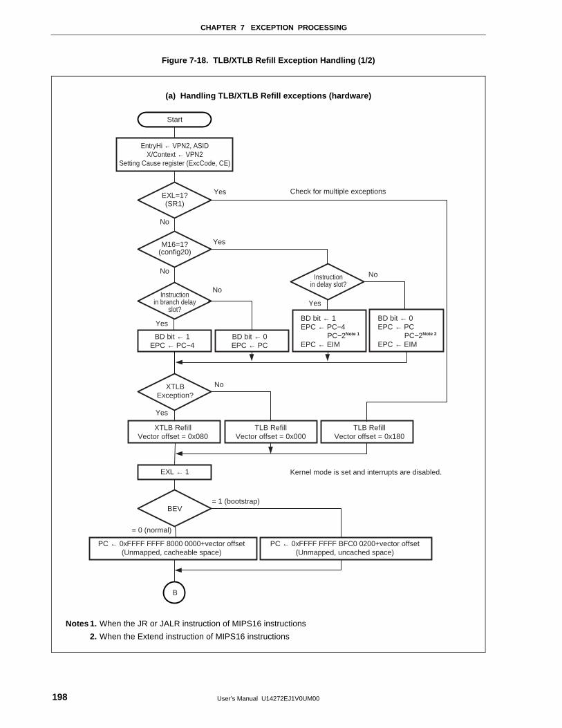
CHAPTER 7 EXCEPTION PROCESSING
User’s Manual U14272EJ1V0UM00198
Figure 7-18. TLB/XTLB Refill Exception Handling (1/2)
(a) Handling TLB/XTLB Refill exceptions (hardware)
YesEXL=1?(SR1)
No
No
Yes
BEV
No
Yes
M16=1?
XTLBException?
XTLB RefillVector offset = 0x080
TLB RefillVector offset = 0x000
TLB RefillVector offset = 0x180
(config20)
No No
Yes
Yes
EXL ← 1
= 0 (normal)
= 1 (bootstrap)
Kernel mode is set and interrupts are disabled.
BD bit ← 1EPC ← PC−4
BD bit ← 0EPC ← PC
Instructionin branch delay
slot?
Instructionin delay slot?
PC ← 0xFFFF FFFF 8000 0000+vector offset(Unmapped, cacheable space)
PC ← 0xFFFF FFFF BFC0 0200+vector offset(Unmapped, uncached space)
BD bit ← 1EPC ← PC−4 PC−2Note 1
EPC ← EIM
BD bit ← 0EPC ← PC PC−2Note 2
EPC ← EIM
Check for multiple exceptions
EntryHi ← VPN2, ASIDX/Context ← VPN2
Setting Cause register (ExcCode, CE)
Start
B
Notes 1. When the JR or JALR instruction of MIPS16 instructions
2. When the Extend instruction of MIPS16 instructions
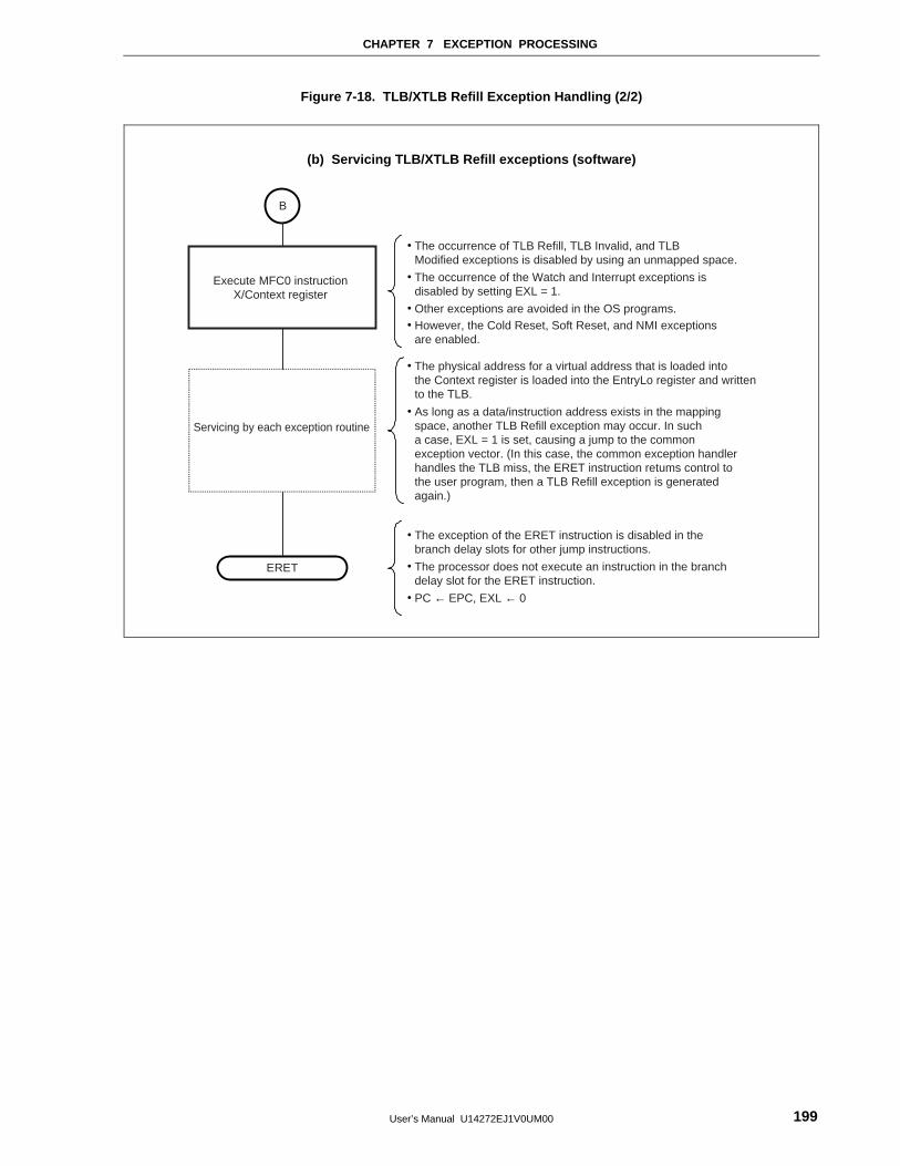
CHAPTER 7 EXCEPTION PROCESSING
User’s Manual U14272EJ1V0UM00 199
Figure 7-18. TLB/XTLB Refill Exception Handling (2/2)
(b) Servicing TLB/XTLB Refill exceptions (software)
Execute MFC0 instructionX/Context register
Servicing by each exception routine
The occurrence of TLB Refill, TLB Invalid, and TLBModified exceptions is disabled by using an unmapped space.
The occurrence of the Watch and Interrupt exceptions isdisabled by setting EXL = 1.
Other exceptions are avoided in the OS programs.
The exception of the ERET instruction is disabled in thebranch delay slots for other jump instructions.
The processor does not execute an instruction in the branchdelay slot for the ERET instruction.
PC ← EPC, EXL ← 0
However, the Cold Reset, Soft Reset, and NMI exceptionsare enabled.
The physical address for a virtual address that is loaded intothe Context register is loaded into the EntryLo register and writtento the TLB.
As long as a data/instruction address exists in the mappingspace, another TLB Refill exception may occur. In sucha case, EXL = 1 is set, causing a jump to the commonexception vector. (In this case, the common exception handlerhandles the TLB miss, the ERET instruction retums control tothe user program, then a TLB Refill exception is generatedagain.)
ERET
B
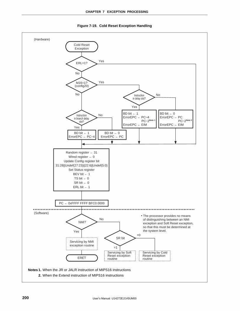
CHAPTER 7 EXCEPTION PROCESSING
User’s Manual U14272EJ1V0UM00200
Figure 7-19. Cold Reset Exception Handling
PC ← 0xFFFF FFFF BFC0 0000
Servicing by NMIexception routine
Servicing by SoftReset exceptionroutine
Servicing by ColdReset exceptionroutine
YesERL=1?
No
No
Yes
Yes
(Software)
(Hardware)
NMI?No
=0
=1
YesM16=1?(config20)
No No
Yes
BD bit ← 1ErrorEPC ← PC−4
BD bit ← 0ErrorEPC ← PC
Instructionin branch delay
slot?
Instructionin delay slot?
BD bit ← 1ErrorEPC ← PC−4 PC−2Note 1
ErrorEPC ← EIM
BD bit ← 0ErrorEPC ← PC PC−2Note 2
ErrorEPC ← EIM
Random register ← 31Wired register ← 0
Update Config register bit31:28||Undef(27:23)||22:6||Undef(5:0)
Set Status registerBEV bit ← 1TS bit ← 0SR bit ← 0
ERL bit ← 1
The processor provides no meansof distinguishing between an NMIexception and Soft Reset exception,so that this must be determined atthe system level.
ERET
SR bit
Cold ResetException
Notes 1. When the JR or JALR instruction of MIPS16 instructions
2. When the Extend instruction of MIPS16 instructions
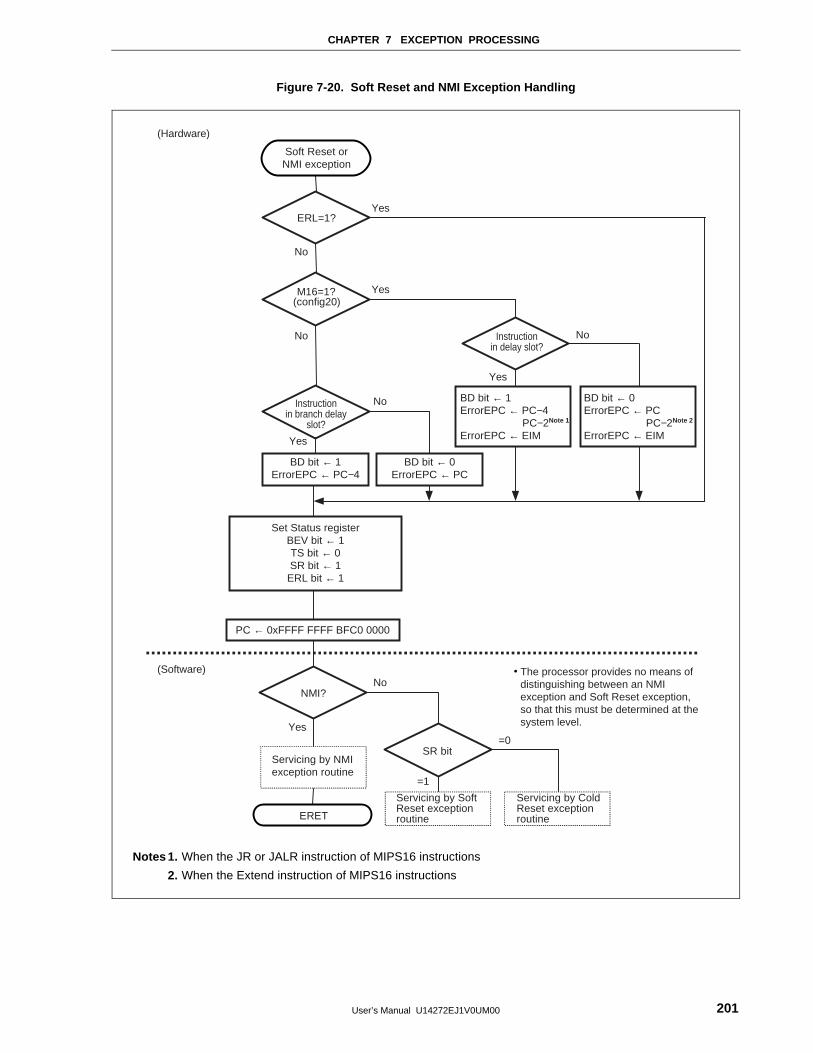
CHAPTER 7 EXCEPTION PROCESSING
User’s Manual U14272EJ1V0UM00 201
Figure 7-20. Soft Reset and NMI Exception Handling
YesERL=1?
No
No
Yes
Yes
(Software)
(Hardware)
NMI?No
=0
=1
No
Yes
YesM16=1?(config20)
No
Instructionin branch delay
slot?
BD bit ← 1ErrorEPC ← PC−4 PC−2Note 1
ErrorEPC ← EIM
BD bit ← 0ErrorEPC ← PC PC−2Note 2
ErrorEPC ← EIM
Instructionin delay slot?
PC ← 0xFFFF FFFF BFC0 0000
Servicing by NMIexception routine
Servicing by SoftReset exceptionroutine
Servicing by ColdReset exceptionroutine
BD bit ← 1ErrorEPC ← PC−4
BD bit ← 0ErrorEPC ← PC
Set Status registerBEV bit ← 1TS bit ← 0SR bit ← 1
ERL bit ← 1
The processor provides no means ofdistinguishing between an NMIexception and Soft Reset exception,so that this must be determined at thesystem level.
ERET
SR bit
Soft Reset orNMI exception
Notes 1. When the JR or JALR instruction of MIPS16 instructions
2. When the Extend instruction of MIPS16 instructions

User’s Manual U14272EJ1V0UM00202
[MEMO]
User’s Manual U14272EJ1V0UM00 203
CHAPTER 8 INITIALIZATION INTERFACE
8.1 Overview
This chapter describes the initialization interface and processor modes. It also explains the reset signal
descriptions and types, signal- and timing-related dependence, and the initialization sequence during each mode that
can be selected by the user.
Remark # that follows signal names indicates active low.
8.2 Reset Function
There are five ways to reset the VR4181. Each is summarized below.
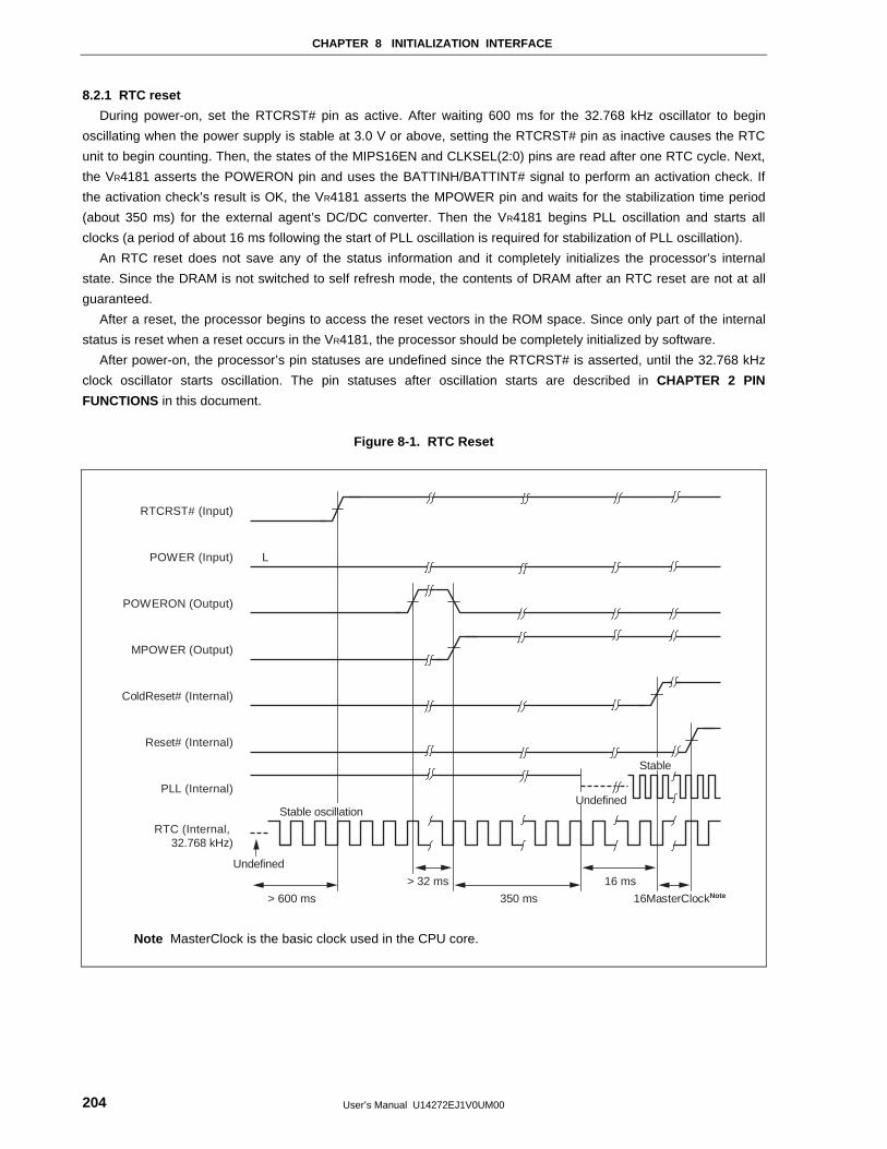
CHAPTER 8 INITIALIZATION INTERFACE
User’s Manual U14272EJ1V0UM00204
8.2.1 RTC reset
During power-on, set the RTCRST# pin as active. After waiting 600 ms for the 32.768 kHz oscillator to begin
oscillating when the power supply is stable at 3.0 V or above, setting the RTCRST# pin as inactive causes the RTC
unit to begin counting. Then, the states of the MIPS16EN and CLKSEL(2:0) pins are read after one RTC cycle. Next,
the VR4181 asserts the POWERON pin and uses the BATTINH/BATTINT# signal to perform an activation check. If
the activation check’s result is OK, the VR4181 asserts the MPOWER pin and waits for the stabilization time period
(about 350 ms) for the external agent’s DC/DC converter. Then the VR4181 begins PLL oscillation and starts all
clocks (a period of about 16 ms following the start of PLL oscillation is required for stabilization of PLL oscillation).
An RTC reset does not save any of the status information and it completely initializes the processor’s internal
state. Since the DRAM is not switched to self refresh mode, the contents of DRAM after an RTC reset are not at all
guaranteed.
After a reset, the processor begins to access the reset vectors in the ROM space. Since only part of the internal
status is reset when a reset occurs in the VR4181, the processor should be completely initialized by software.
After power-on, the processor’s pin statuses are undefined since the RTCRST# is asserted, until the 32.768 kHz
clock oscillator starts oscillation. The pin statuses after oscillation starts are described in CHAPTER 2 PIN
FUNCTIONS in this document.
Figure 8-1. RTC Reset
L
16MasterClockNote
Reset# (Internal)
ColdReset# (Internal)
MPOWER (Output)
Undefined
POWER (Input)
RTCRST# (Input)
RTC (Internal, 32.768 kHz)
16 ms
> 600 ms
PLL (Internal)
> 32 ms
POWERON (Output)
350 ms
Stable oscillation
Stable
Undefined
Note MasterClock is the basic clock used in the CPU core.
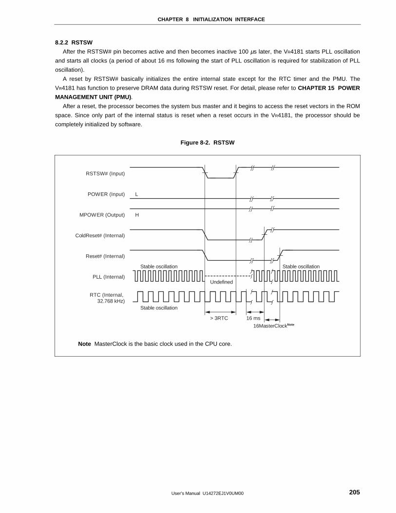
CHAPTER 8 INITIALIZATION INTERFACE
User’s Manual U14272EJ1V0UM00 205
8.2.2 RSTSW
After the RSTSW# pin becomes active and then becomes inactive 100 µs later, the VR4181 starts PLL oscillation
and starts all clocks (a period of about 16 ms following the start of PLL oscillation is required for stabilization of PLL
oscillation).
A reset by RSTSW# basically initializes the entire internal state except for the RTC timer and the PMU. The
VR4181 has function to preserve DRAM data during RSTSW reset. For detail, please refer to CHAPTER 15 POWER
MANAGEMENT UNIT (PMU) .
After a reset, the processor becomes the system bus master and it begins to access the reset vectors in the ROM
space. Since only part of the internal status is reset when a reset occurs in the VR4181, the processor should be
completely initialized by software.
Figure 8-2. RSTSW
L
16MasterClockNote
Reset# (Internal)
ColdReset# (Internal)
MPOWER (Output)
POWER (Input)
RSTSW# (Input)
16 ms
PLL (Internal)
> 3RTC
H
Stable oscillation
Stable oscillation
Undefined
Stable oscillation
RTC (Internal, 32.768 kHz)
Note MasterClock is the basic clock used in the CPU core.
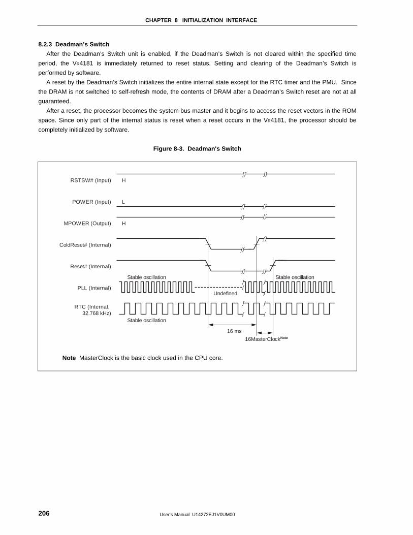
CHAPTER 8 INITIALIZATION INTERFACE
User’s Manual U14272EJ1V0UM00206
8.2.3 Deadman’s Switch
After the Deadman’s Switch unit is enabled, if the Deadman’s Switch is not cleared within the specified time
period, the VR4181 is immediately returned to reset status. Setting and clearing of the Deadman’s Switch is
performed by software.
A reset by the Deadman’s Switch initializes the entire internal state except for the RTC timer and the PMU. Since
the DRAM is not switched to self-refresh mode, the contents of DRAM after a Deadman’s Switch reset are not at all
guaranteed.
After a reset, the processor becomes the system bus master and it begins to access the reset vectors in the ROM
space. Since only part of the internal status is reset when a reset occurs in the VR4181, the processor should be
completely initialized by software.
Figure 8-3. Deadman's Switch
L
16MasterClockNote
Reset# (Internal)
ColdReset# (Internal)
MPOWER (Output)
POWER (Input)
RSTSW# (Input)
RTC (Internal, 32.768 kHz)
16 ms
PLL (Internal)
H
Stable oscillation
Stable oscillation
Undefined
Stable oscillation
H
Note MasterClock is the basic clock used in the CPU core.
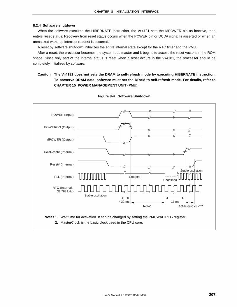
CHAPTER 8 INITIALIZATION INTERFACE
User’s Manual U14272EJ1V0UM00 207
8.2.4 Software shutdown
When the software executes the HIBERNATE instruction, the VR4181 sets the MPOWER pin as inactive, then
enters reset status. Recovery from reset status occurs when the POWER pin or DCD# signal Is asserted or when an
unmasked wake-up interrupt request is occurred.
A reset by software shutdown initializes the entire internal state except for the RTC timer and the PMU.
After a reset, the processor becomes the system bus master and it begins to access the reset vectors in the ROM
space. Since only part of the internal status is reset when a reset occurs in the VR4181, the processor should be
completely initialized by software.
Cauiton The V R4181 does not sets the DRAM to self-refresh mode by executing HIBERNATE instruction.
To preserve DRAM data, software must set the DRAM to self-refresh mode. For details, refer to
CHAPTER 15 POWER MANAGEMENT UNIT (PMU).
Figure 8-4. Software Shutdown
16MasterClockNote2
Reset# (Internal)
ColdReset# (Internal)
MPOWER (Output)
POWER (Input)
RTC (Internal, 32.768 kHz)
16 ms
PLL (Internal)
> 32 ms
POWERON (Output)
Note1
Stable oscillation
UndefinedStopped
Stable oscillation
Notes 1. Wait time for activation. It can be changed by setting the PMUWAITREG register.
2. MasterClock is the basic clock used in the CPU core.
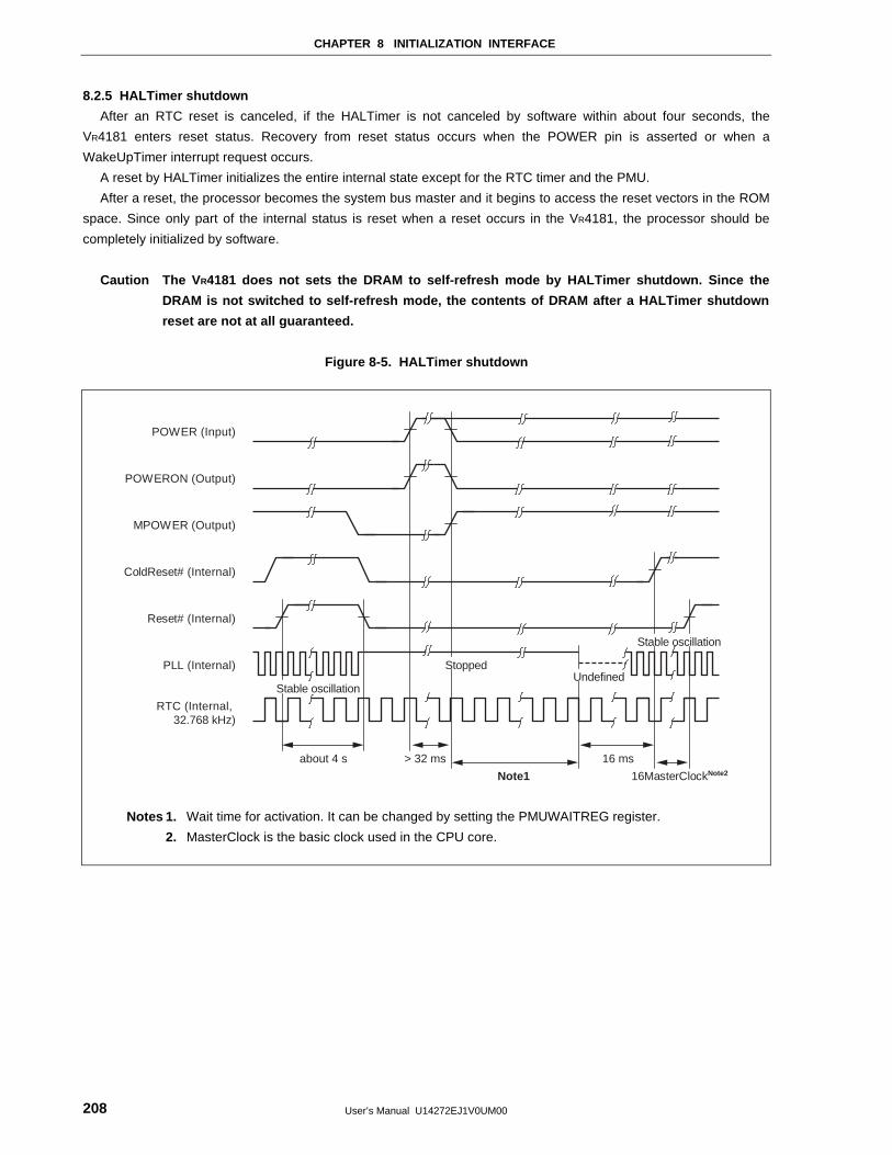
CHAPTER 8 INITIALIZATION INTERFACE
User’s Manual U14272EJ1V0UM00208
8.2.5 HALTimer shutdown
After an RTC reset is canceled, if the HALTimer is not canceled by software within about four seconds, the
VR4181 enters reset status. Recovery from reset status occurs when the POWER pin is asserted or when a
WakeUpTimer interrupt request occurs.
A reset by HALTimer initializes the entire internal state except for the RTC timer and the PMU.
After a reset, the processor becomes the system bus master and it begins to access the reset vectors in the ROM
space. Since only part of the internal status is reset when a reset occurs in the VR4181, the processor should be
completely initialized by software.
Caution The V R4181 does not sets the DRAM to self-refresh mode by HALTimer shutdown. Since the
DRAM is not switched to self-refresh mode, the contents of DRAM after a HALTimer shutdown
reset are not at all guaranteed.
Figure 8-5. HALTimer shutdown
16MasterClockNote2
Reset# (Internal)
ColdReset# (Internal)
MPOWER (Output)
POWER (Input)
RTC (Internal, 32.768 kHz)
16 ms
PLL (Internal)
> 32 ms
POWERON (Output)
Note1
UndefinedStopped
Stable oscillation
about 4 s
Stable oscillation
Notes 1. Wait time for activation. It can be changed by setting the PMUWAITREG register.
2. MasterClock is the basic clock used in the CPU core.
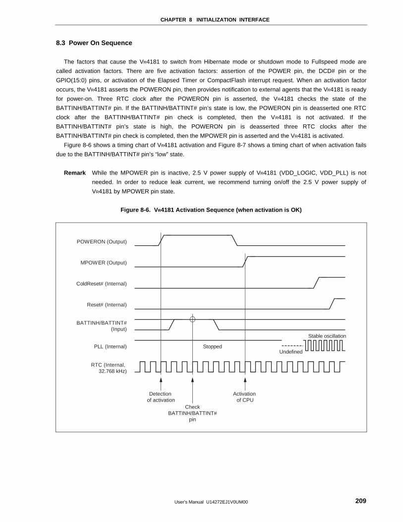
CHAPTER 8 INITIALIZATION INTERFACE
User’s Manual U14272EJ1V0UM00 209
8.3 Power On Sequence
The factors that cause the VR4181 to switch from Hibernate mode or shutdown mode to Fullspeed mode are
called activation factors. There are five activation factors: assertion of the POWER pin, the DCD# pin or the
GPIO(15:0) pins, or activation of the Elapsed Timer or CompactFlash interrupt request. When an activation factor
occurs, the VR4181 asserts the POWERON pin, then provides notification to external agents that the VR4181 is ready
for power-on. Three RTC clock after the POWERON pin is asserted, the VR4181 checks the state of the
BATTINH/BATTINT# pin. If the BATTINH/BATTINT# pin’s state is low, the POWERON pin is deasserted one RTC
clock after the BATTINH/BATTINT# pin check is completed, then the VR4181 is not activated. If the
BATTINH/BATTINT# pin’s state is high, the POWERON pin is deasserted three RTC clocks after the
BATTINH/BATTINT# pin check is completed, then the MPOWER pin is asserted and the VR4181 is activated.
Figure 8-6 shows a timing chart of VR4181 activation and Figure 8-7 shows a timing chart of when activation fails
due to the BATTINH/BATTINT# pin’s “low” state.
Remark While the MPOWER pin is inactive, 2.5 V power supply of VR4181 (VDD_LOGIC, VDD_PLL) is not
needed. In order to reduce leak current, we recommend turning on/off the 2.5 V power supply of
VR4181 by MPOWER pin state.
Figure 8-6. V R4181 Activation Sequence (when activation is OK)
Reset# (Internal)
ColdReset# (Internal)
MPOWER (Output)
BATTINH/BATTINT# (Input)
RTC (Internal, 32.768 kHz)
Activation of CPU
PLL (Internal)
CheckBATTINH/BATTINT#
pin
POWERON (Output)
UndefinedStopped
Stable oscillation
Detection of activation
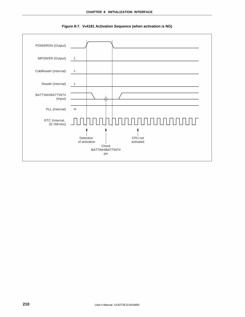
CHAPTER 8 INITIALIZATION INTERFACE
User’s Manual U14272EJ1V0UM00210
Figure 8-7. V R4181 Activation Sequence (when activation is NG)
Reset# (Internal)
ColdReset# (Internal)
MPOWER (Output)
BATTINH/BATTINT# (Input)
RTC (Internal, 32.768 kHz)
CPU notactivated
PLL (Internal)
CheckBATTINH/BATTINT#
pin
POWERON (Output)
H
Detection of activation
L
L
L
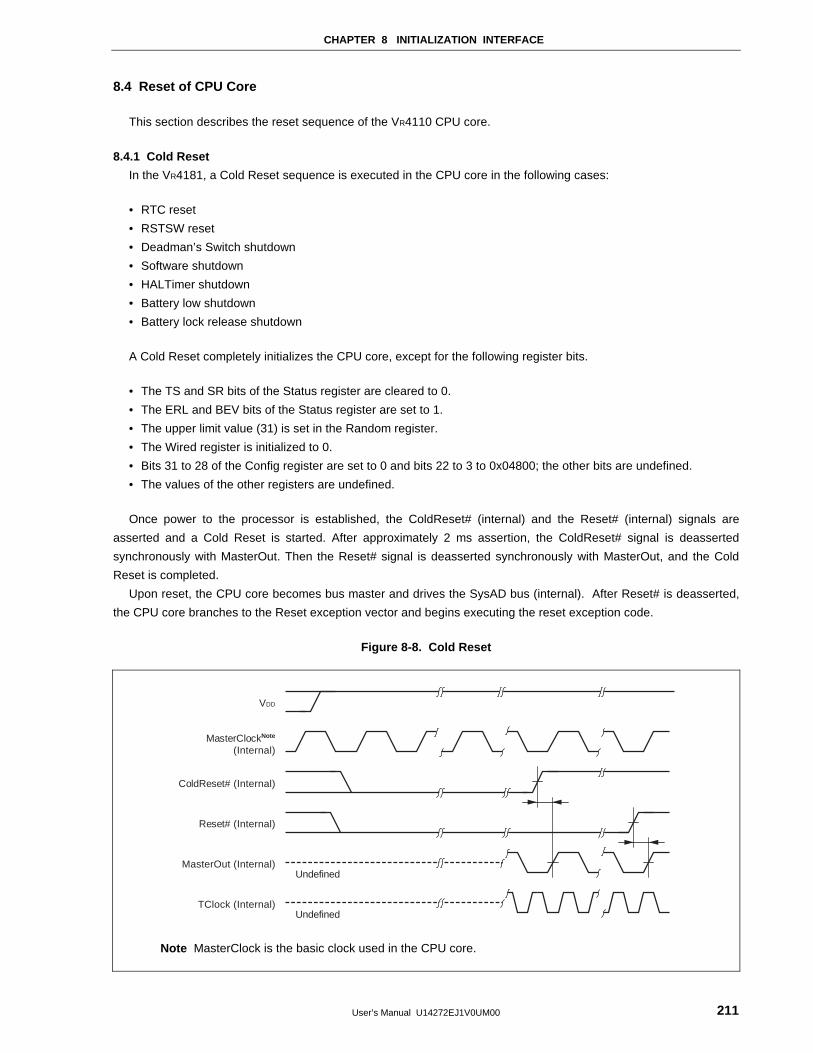
CHAPTER 8 INITIALIZATION INTERFACE
User’s Manual U14272EJ1V0UM00 211
8.4 Reset of CPU Core
This section describes the reset sequence of the VR4110 CPU core.
8.4.1 Cold Reset
In the VR4181, a Cold Reset sequence is executed in the CPU core in the following cases:
• RTC reset
• RSTSW reset
• Deadman’s Switch shutdown
• Software shutdown
• HALTimer shutdown
• Battery low shutdown
• Battery lock release shutdown
A Cold Reset completely initializes the CPU core, except for the following register bits.
• The TS and SR bits of the Status register are cleared to 0.
• The ERL and BEV bits of the Status register are set to 1.
• The upper limit value (31) is set in the Random register.
• The Wired register is initialized to 0.
• Bits 31 to 28 of the Config register are set to 0 and bits 22 to 3 to 0x04800; the other bits are undefined.
• The values of the other registers are undefined.
Once power to the processor is established, the ColdReset# (internal) and the Reset# (internal) signals are
asserted and a Cold Reset is started. After approximately 2 ms assertion, the ColdReset# signal is deasserted
synchronously with MasterOut. Then the Reset# signal is deasserted synchronously with MasterOut, and the Cold
Reset is completed.
Upon reset, the CPU core becomes bus master and drives the SysAD bus (internal). After Reset# is deasserted,
the CPU core branches to the Reset exception vector and begins executing the reset exception code.
Figure 8-8. Cold Reset
Reset# (Internal)
ColdReset# (Internal)
MasterClockNote
(Internal)
VDD
TClock (Internal)
MasterOut (Internal)Undefined
Undefined
Note MasterClock is the basic clock used in the CPU core.
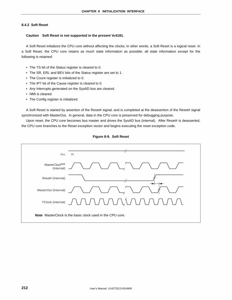
CHAPTER 8 INITIALIZATION INTERFACE
User’s Manual U14272EJ1V0UM00212
8.4.2 Soft Reset
Caution Soft Reset is not supported in the present V R4181.
A Soft Reset initializes the CPU core without affecting the clocks; in other words, a Soft Reset is a logical reset. In
a Soft Reset, the CPU core retains as much state information as possible; all state information except for the
following is retained:
• The TS bit of the Status register is cleared to 0.
• The SR, ERL and BEV bits of the Status register are set to 1.
• The Count register is initialized to 0.
• The IP7 bit of the Cause register is cleared to 0.
• Any Interrupts generated on the SysAD bus are cleared.
• NMI is cleared.
• The Config register is initialized.
A Soft Reset is started by assertion of the Reset# signal, and is completed at the deassertion of the Reset# signal
synchronized with MasterOut. In general, data in the CPU core is preserved for debugging purpose.
Upon reset, the CPU core becomes bus master and drives the SysAD bus (internal). After Reset# is deasserted,
the CPU core branches to the Reset exception vector and begins executing the reset exception code.
Figure 8-9. Soft Reset
Reset# (Internal)
MasterClockNote
(Internal)
VDD
TClock (Internal)
MasterOut (Internal)
H
Note MasterClock is the basic clock used in the CPU core.
CHAPTER 8 INITIALIZATION INTERFACE
User’s Manual U14272EJ1V0UM00 213
8.5 VR4181 Processor Modes
The VR4181 supports various modes, which can be selected by the user. The CPU core mode is set each time a
write occurs in the Status register and Config register. The modes of on-chip peripheral circuits are set by writing to
the I/O register.
This section describes the CPU core’s operation modes. For operation modes of on-chip peripheral circuits, see
the chapters describing the various units.
8.5.1 Power modes
The VR4181 supports four power modes: Fullspeed mode, Standby mode, Suspend mode, and Hibernate mode.
(1) Fullspeed mode
This is the normal operation mode.
The VR4181’s default status sets operation under Fullspeed mode. After the processor is reset, the VR4181
returns to Fullspeed mode.
(2) Standby mode
When a STANDBY instruction has been executed, the processor can be set to Standby mode. During Standby
mode, all of the internal clocks in the CPU core except for the timer, interrupt, memory controller and LCD
controller clocks are held at high level. The peripheral units all operate as they do during Fullspeed mode. This
means that DMA operations are enabled during Standby mode.
When the STANDBY instruction completes the WB stage, the VR4181 remains idle until the SysAD internal bus
enters the idle state. Next, the clocks in the CPU core are shut down and pipeline operation is stopped. However,
the PLL, timer, interrupt, memory controller and LCD controller clocks continue to operate, as do the internal bus
clocks (SClock, TClock, and MasterOut).
During Standby mode, the processor returns to Fullspeed mode if any interrupt request occurs, including a timer
interrupt that occurs internally.
(3) Suspend mode
When the SUSPEND instruction has been executed, the processor can be set to Suspend mode. During
Suspend mode, the processor stalls the pipeline and all of the internal clocks in the CPU core except for PLL
timer and interrupt clocks are held at high level. The VR4181 stops supplying TClock to peripheral units.
Accordingly, during Suspend mode peripheral units can only be activated by a special interrupt unit (DCD#
control, etc.). While in this mode, the register and cache contents are retained.
When the SUSPEND instruction completes the WB stage, the VR4181 waits for the SysAD internal bus to enter
the idle state. Next, the clocks in the CPU core are shut down and pipeline operation is stopped. The VR4181
then stops supplying TClock to peripheral units. However, the PLL, timer, and interrupt clocks continue to
operate, as do the MasterOut.
The processor remains in Suspend mode until an interrupt request is received, at which time it returns to
Fullspeed mode.
CHAPTER 8 INITIALIZATION INTERFACE
User’s Manual U14272EJ1V0UM00214
(4) Hibernate mode
When the HIBERNATE instruction has been executed, the processor can be set to Hibernate mode. During
Hibernate mode, the processor stops supplying clocks to all units. The register and cache contents are retained
and output of TClock and MasterOut is stopped.
The processor remains in Hibernate mode until occurrence of an activation factor, which is assertion of the
POWER pin or the DCD# pin, or activation of the Elapsed Timer interrupt request etc. When the activation factor
occurs, the processor returns to Fullspeed mode.
Power consumption during Hibernate mode is about 0 W (it does not go completely to 0 W due to the existence
of a 32.768 kHz oscillator or on-chip peripheral circuits that operate at 32.768 kHz).
8.5.2 Privilege mode
The VR4181 supports three system modes: kernel expanded addressing mode, supervisor expanded addressing
mode, and user expanded addressing mode. These three modes are described below.
(1) Kernel expanded addressing mode
When the Status register’s KX bit has been set, an Expanded TLB Refill exception vector is used when a TLB
refill occurs for the kernel address. While in Kernel mode, the MIPS III operation code can always be used,
regardless of the KX bit.
(2) Supervisor expanded addressing mode
When the Status register’s SX bit has been set, the MIPS III operation code can be used in Supervisor mode and
an Expanded TLB Refill exception vector is used when a TLB refill occurs for the Supervisor address.
(3) User expanded addressing mode
When the Status register’s UX bit has been set, the MIPS III operation code can be used in User mode, and an
Expanded TLB Refill exception vector is used when a TLB refill occurs for the User address. When this bit is
cleared, the MIPS I and II operation codes can be used, as can 32-bit virtual addresses.
8.5.3 Reverse endian
When the Status register’s RE bit has been set, the endian ordering is reversed to adopt the user software’s
perspective. However, the RE bit of the Status register must be set to 0 since the VR4181 supports the little-endian
order only.
8.5.4 Bootstrap exception vector (BEV)
The BEV bit is used to generate an exception during operation testing (diagnostic testing) of the cache and main
memory system.
When the Status register’s BEV bit has been set, the address of the TLB Refill exception vector is changed to the
virtual address 0xFFFF FFFF BFC0 0200 and the ordinary exception vector is changed to address 0xFFFF FFFF
BFC0 0380.
When the BEV bit is cleared, the TLB miss exception vector’s address is changed to 0xFFFF FFFF 8000 0000
and the ordinary exception vector is changed to address 0xFFFF FFFF 8000 0180.
CHAPTER 8 INITIALIZATION INTERFACE
User’s Manual U14272EJ1V0UM00 215
8.5.5 Cache error check
The CE bit of the Status register is meaningless because the VR4181 has no cache parity.
8.5.6 Parity error prohibit
The VR4181 processor does not issue any cache parity error exceptions regardless of the DE bit of the Status
register.
8.5.7 Interrupt enable (IE)
When the Status register’s IE bit has been cleared, no interrupts can be received except for reset interrupt and
non-maskable interrupt requests.

User’s Manual U14272EJ1V0UM00216
[MEMO]
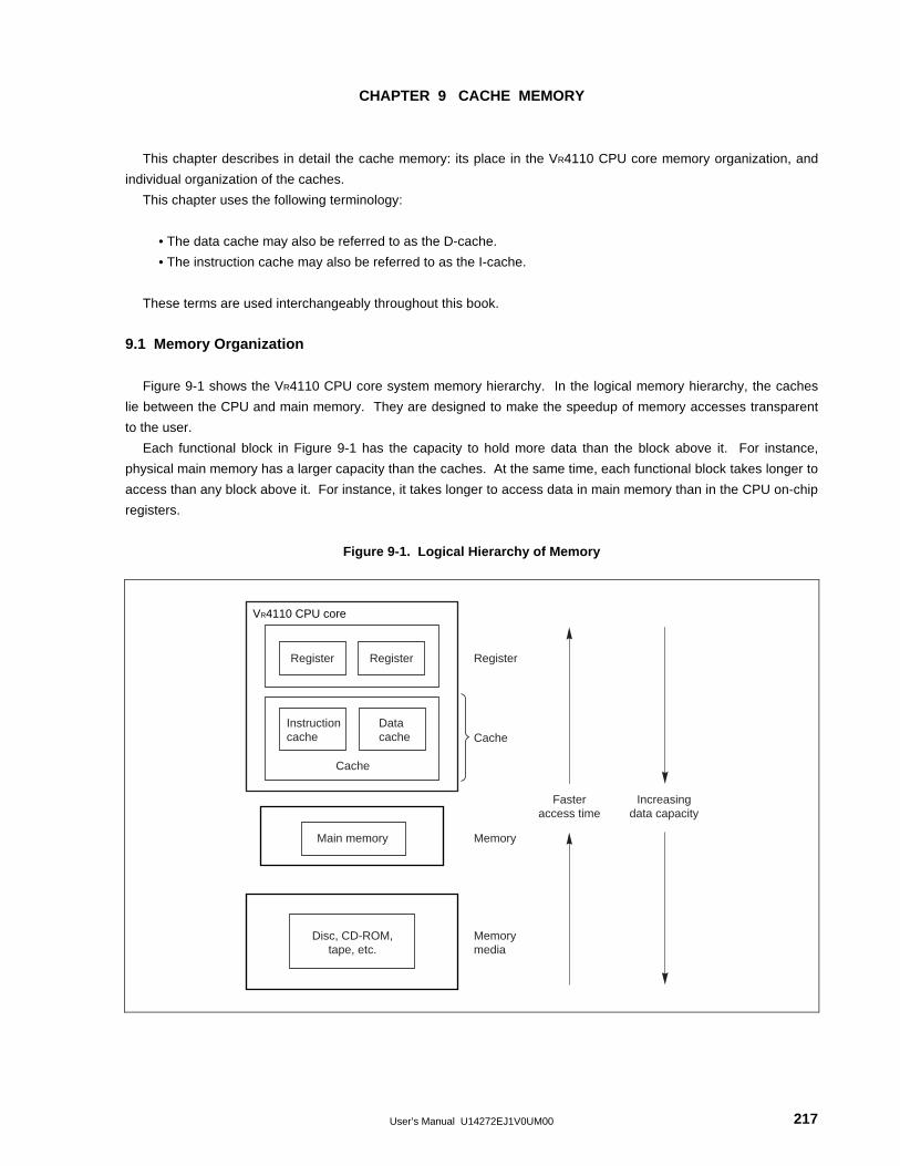
User’s Manual U14272EJ1V0UM00 217
CHAPTER 9 CACHE MEMORY
This chapter describes in detail the cache memory: its place in the VR4110 CPU core memory organization, and
individual organization of the caches.
This chapter uses the following terminology:
• The data cache may also be referred to as the D-cache.
• The instruction cache may also be referred to as the I-cache.
These terms are used interchangeably throughout this book.
9.1 Memory Organization
Figure 9-1 shows the VR4110 CPU core system memory hierarchy. In the logical memory hierarchy, the caches
lie between the CPU and main memory. They are designed to make the speedup of memory accesses transparent
to the user.
Each functional block in Figure 9-1 has the capacity to hold more data than the block above it. For instance,
physical main memory has a larger capacity than the caches. At the same time, each functional block takes longer to
access than any block above it. For instance, it takes longer to access data in main memory than in the CPU on-chip
registers.
Figure 9-1. Logical Hierarchy of Memory
VR4110 CPU core
Register Register
Cache
Register
Memory
Fasteraccess time
Increasingdata capacity
Memorymedia
Instructioncache
Datacache
Cache
Main memory
Disc, CD-ROM,tape, etc.
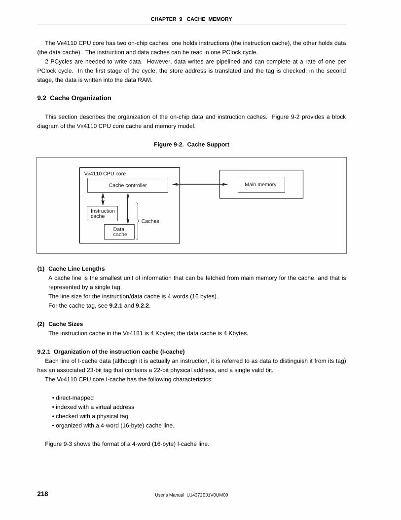
CHAPTER 9 CACHE MEMORY
User’s Manual U14272EJ1V0UM00218
The VR4110 CPU core has two on-chip caches: one holds instructions (the instruction cache), the other holds data
(the data cache). The instruction and data caches can be read in one PClock cycle.
2 PCycles are needed to write data. However, data writes are pipelined and can complete at a rate of one per
PClock cycle. In the first stage of the cycle, the store address is translated and the tag is checked; in the second
stage, the data is written into the data RAM.
9.2 Cache Organization
This section describes the organization of the on-chip data and instruction caches. Figure 9-2 provides a block
diagram of the VR4110 CPU core cache and memory model.
Figure 9-2. Cache Support
VR4110 CPU core
Cache controller
Datacache
Instructioncache
Caches
Main memory
(1) Cache Line Lengths
A cache line is the smallest unit of information that can be fetched from main memory for the cache, and that is
represented by a single tag.
The line size for the instruction/data cache is 4 words (16 bytes).
For the cache tag, see 9.2.1 and 9.2.2.
(2) Cache Sizes
The instruction cache in the VR4181 is 4 Kbytes; the data cache is 4 Kbytes.
9.2.1 Organization of the instruction cache (I-cache)
Each line of I-cache data (although it is actually an instruction, it is referred to as data to distinguish it from its tag)
has an associated 23-bit tag that contains a 22-bit physical address, and a single valid bit.
The VR4110 CPU core I-cache has the following characteristics:
• direct-mapped
• indexed with a virtual address
• checked with a physical tag
• organized with a 4-word (16-byte) cache line.
Figure 9-3 shows the format of a 4-word (16-byte) I-cache line.
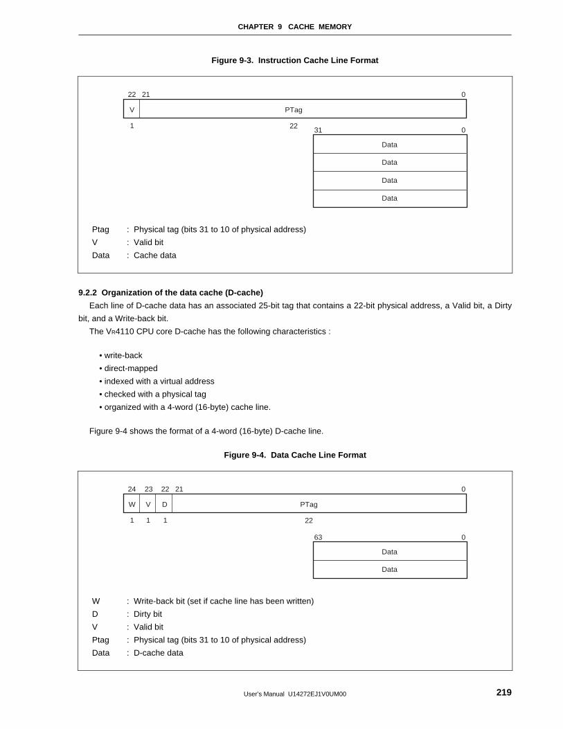
CHAPTER 9 CACHE MEMORY
User’s Manual U14272EJ1V0UM00 219
Figure 9-3. Instruction Cache Line Format
22 21
PTagV
0
1 22
Data
0
Data
Data
Data
31
Ptag : Physical tag (bits 31 to 10 of physical address)
V : Valid bit
Data : Cache data
9.2.2 Organization of the data cache (D-cache)
Each line of D-cache data has an associated 25-bit tag that contains a 22-bit physical address, a Valid bit, a Dirty
bit, and a Write-back bit.
The VR4110 CPU core D-cache has the following characteristics :
• write-back
• direct-mapped
• indexed with a virtual address
• checked with a physical tag
• organized with a 4-word (16-byte) cache line.
Figure 9-4 shows the format of a 4-word (16-byte) D-cache line.
Figure 9-4. Data Cache Line Format
24 23
PTagW
0
1 22
Data
0
Data
63
22 21
1 1
V D
W : Write-back bit (set if cache line has been written)
D : Dirty bit
V : Valid bit
Ptag : Physical tag (bits 31 to 10 of physical address)
Data : D-cache data
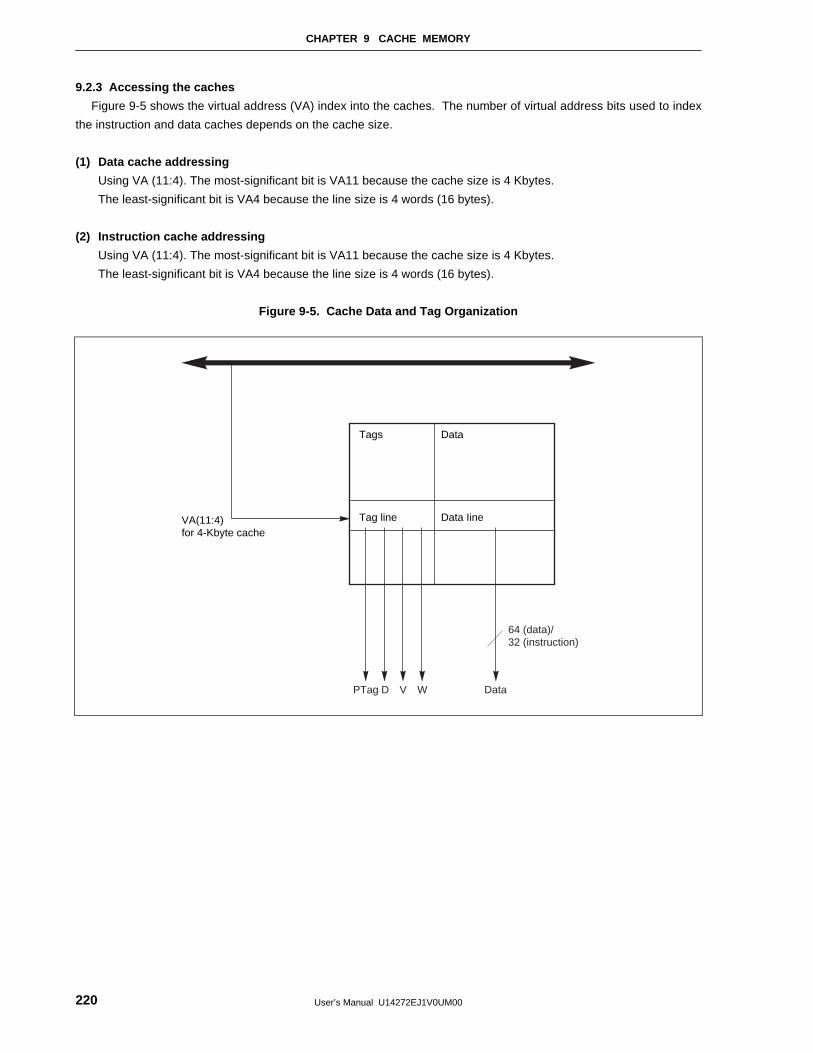
CHAPTER 9 CACHE MEMORY
User’s Manual U14272EJ1V0UM00220
9.2.3 Accessing the caches
Figure 9-5 shows the virtual address (VA) index into the caches. The number of virtual address bits used to index
the instruction and data caches depends on the cache size.
(1) Data cache addressing
Using VA (11:4). The most-significant bit is VA11 because the cache size is 4 Kbytes.
The least-significant bit is VA4 because the line size is 4 words (16 bytes).
(2) Instruction cache addressing
Using VA (11:4). The most-significant bit is VA11 because the cache size is 4 Kbytes.
The least-significant bit is VA4 because the line size is 4 words (16 bytes).
Figure 9-5. Cache Data and Tag Organization
D V W DataPTag
64 (data)/32 (instruction)
Tags Data
Tag line Data IineVA(11:4)for 4-Kbyte cache
CHAPTER 9 CACHE MEMORY
User’s Manual U14272EJ1V0UM00 221
9.3 Cache Operations
As described earlier, caches provide fast temporary data storage, and they make the speedup of memory
accesses transparent to the user. In general, the CPU core accesses cache-resident instructions or data through the
following procedure:
1. The CPU core, through the on-chip cache controller, attempts to access the next instruction or data in the
appropriate cache.
2. The cache controller checks to see if this instruction or data is present in the cache.
• If the instruction/data is present, the CPU core retrieves it. This is called a cache hit.
• If the instruction/data is not present in the cache, the cache controller must retrieve it from memory. This is
called a cache miss.
3. The CPU core retrieves the instruction/data from the cache and operation continues.
It is possible for the same data to be in two places simultaneously: main memory and cache. This data is kept
consistent through the use of a write-back methodology; that is, modified data is not written back to memory until the
cache line is to be replaced.
Instruction and data cache line replacement operations are described in the following sections.
9.3.1 Cache write policy
The VR4110 CPU core manages its data cache by using a write-back policy; that is, it stores write data into the
cache, instead of writing it directly to memoryNote. Some time later this data is independently written into memory. In
the VR4181 implementation, a modified cache line is not written back to memory until the cache line is to be replaced
either in the course of satisfying a cache miss, or during the execution of a write-back CACHE instruction.
When the CPU core writes a cache line back to memory, it does not ordinarily retain a copy of the cache line, and
the state of the cache line is changed to invalid.
Note Contrary to the write-back, the write-through cache policy stores write data into the memory and cache
simultaneously.
CHAPTER 9 CACHE MEMORY
User’s Manual U14272EJ1V0UM00222
9.4 Cache States
(1) Cache line
The three terms below are used to describe the state of a cache line:
• Dirty: a cache line containing data that has changed since it was loaded from memory.
• Clean: a cache line that contains data that has not changed since it was loaded from memory.
• Invalid: a cache line that does not contain valid information must be marked invalid, and cannot be used. For
example, after a Soft Reset, software sets all cache lines to invalid. A cache line in any other state than
invalid is assumed to contain valid information. Neither Cold Reset nor Soft Reset makes the cache state
invalid. Software makes the cache state invalid.
(2) Data cache
The data cache supports three cache states:
• invalid
• valid clean
• valid dirty
(3) Instruction cache
The instruction cache supports two cache states:
• invalid
• valid
The state of a valid cache line may be modified when the processor executes a CACHE operation. CACHE
operations are described in CHAPTER 27 MIPS III INSTRUCTION SET DETAILS .
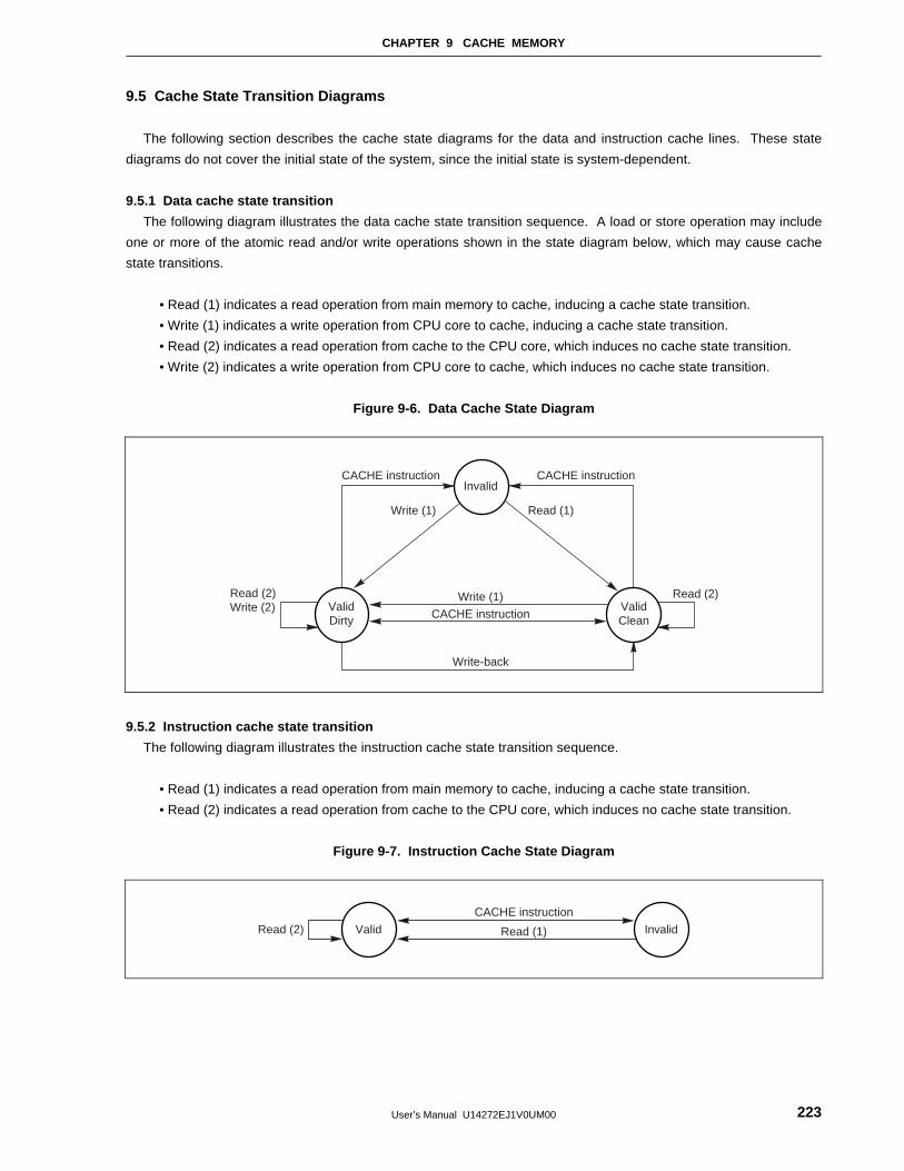
CHAPTER 9 CACHE MEMORY
User’s Manual U14272EJ1V0UM00 223
9.5 Cache State Transition Diagrams
The following section describes the cache state diagrams for the data and instruction cache lines. These state
diagrams do not cover the initial state of the system, since the initial state is system-dependent.
9.5.1 Data cache state transition
The following diagram illustrates the data cache state transition sequence. A load or store operation may include
one or more of the atomic read and/or write operations shown in the state diagram below, which may cause cache
state transitions.
• Read (1) indicates a read operation from main memory to cache, inducing a cache state transition.
• Write (1) indicates a write operation from CPU core to cache, inducing a cache state transition.
• Read (2) indicates a read operation from cache to the CPU core, which induces no cache state transition.
• Write (2) indicates a write operation from CPU core to cache, which induces no cache state transition.
Figure 9-6. Data Cache State Diagram
Write (1)
CACHE instruction
Write-back
Read (2)Read (2)Write (2)
CACHE instruction
Write (1) Read (1)
CACHE instructionInvalid
ValidDirty
ValidClean
9.5.2 Instruction cache state transition
The following diagram illustrates the instruction cache state transition sequence.
• Read (1) indicates a read operation from main memory to cache, inducing a cache state transition.
• Read (2) indicates a read operation from cache to the CPU core, which induces no cache state transition.
Figure 9-7. Instruction Cache State Diagram
Valid Read (1)
CACHE instruction
Read (2) Invalid
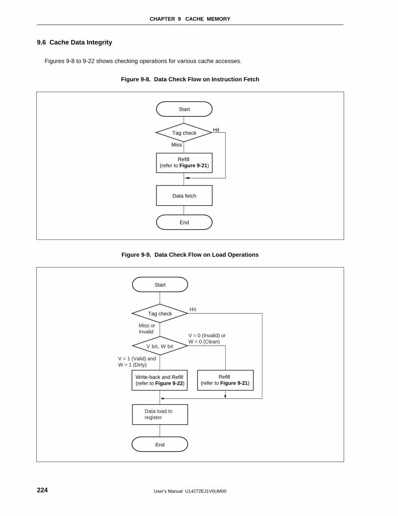
CHAPTER 9 CACHE MEMORY
User’s Manual U14272EJ1V0UM00224
9.6 Cache Data Integrity
Figures 9-8 to 9-22 shows checking operations for various cache accesses.
Figure 9-8. Data Check Flow on Instruction Fetch
Start
End
Miss
Hit
Refill (refer to Figure 9-21 )
Data fetch
Tag check
Figure 9-9. Data Check Flow on Load Operations
Miss orInvalid
V = 1 (Valid) andW = 1 (Dirty)
V = 0 (Invalid) orW = 0 (Clean)
Hit
Start
End
Tag check
V bit, W bit
Write-back and Refill (refer to Figure 9-22 )
Data load toregister
Refill (refer to Figure 9-21 )
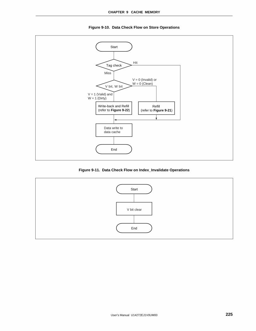
CHAPTER 9 CACHE MEMORY
User’s Manual U14272EJ1V0UM00 225
Figure 9-10. Data Check Flow on Store Operations
Miss
V = 1 (Valid) andW = 1 (Dirty)
V = 0 (Invalid) orW = 0 (Clean)
Hit
Start
End
Tag check
V bit, W bit
Write-back and Refill (refer to Figure 9-22 )
Data write todata cache
Refill (refer to Figure 9-21 )
Figure 9-11. Data Check Flow on Index_Invalidate Operations
Start
End
V bit clear
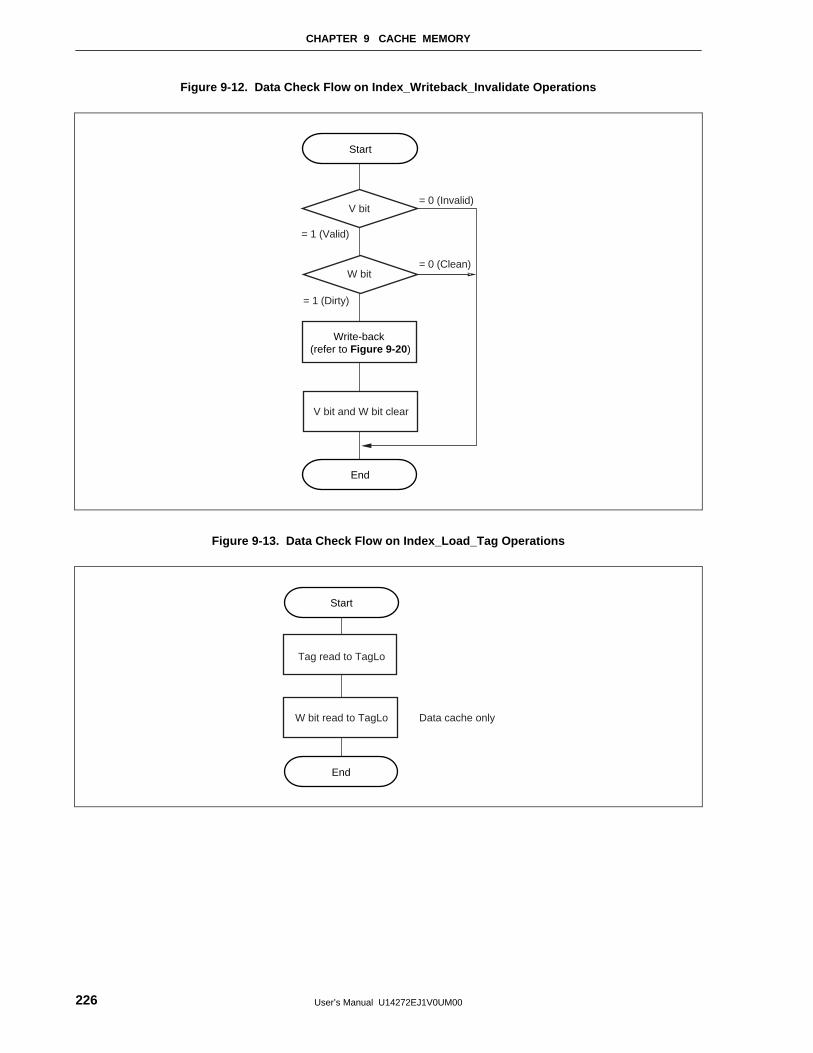
CHAPTER 9 CACHE MEMORY
User’s Manual U14272EJ1V0UM00226
Figure 9-12. Data Check Flow on Index_Writeback_Invalidate Operations
= 1 (Valid)
= 0 (Invalid)
= 0 (Clean)
= 1 (Dirty)
Start
End
V bit
W bit
Write-back (refer to Figure 9-20 )
V bit and W bit clear
Figure 9-13. Data Check Flow on Index_Load_Tag Operations
Data cache only
Start
End
Tag read to TagLo
W bit read to TagLo
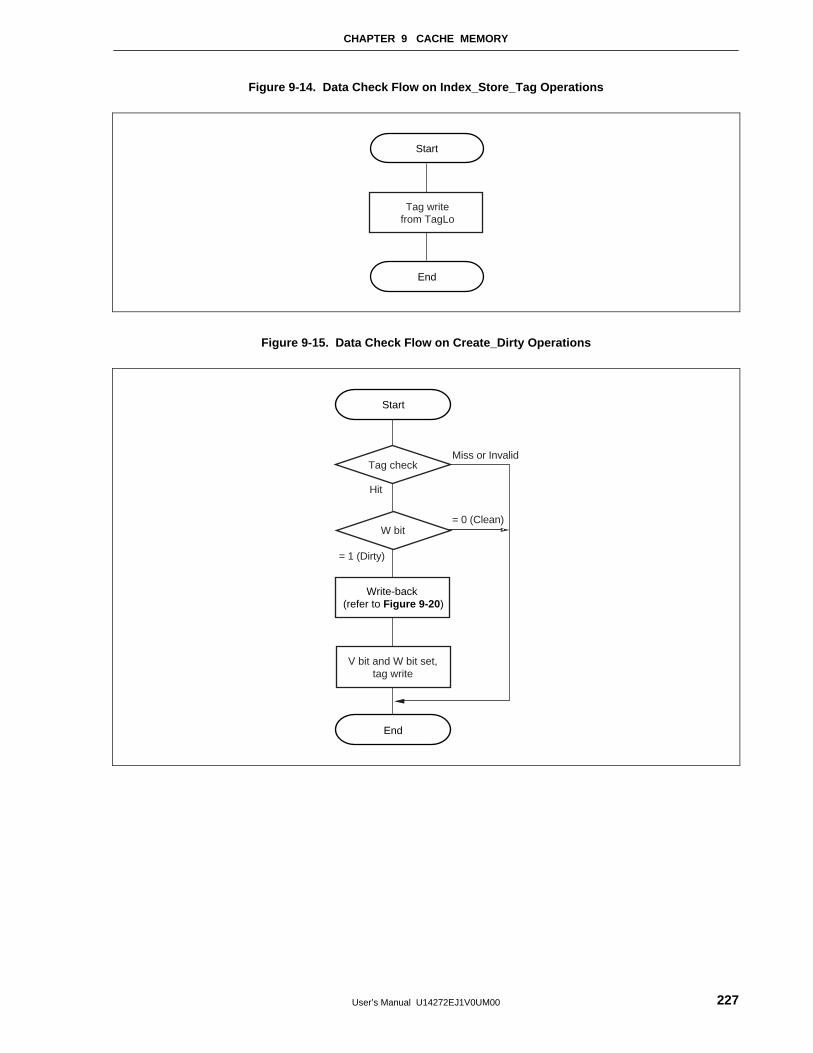
CHAPTER 9 CACHE MEMORY
User’s Manual U14272EJ1V0UM00 227
Figure 9-14. Data Check Flow on Index_Store_Tag Operations
Start
End
Tag writefrom TagLo
Figure 9-15. Data Check Flow on Create_Dirty Operations
Miss or Invalid
Hit
= 0 (Clean)
= 1 (Dirty)
Start
End
Write-back (refer to Figure 9-20 )
Tag check
W bit
V bit and W bit set,tag write
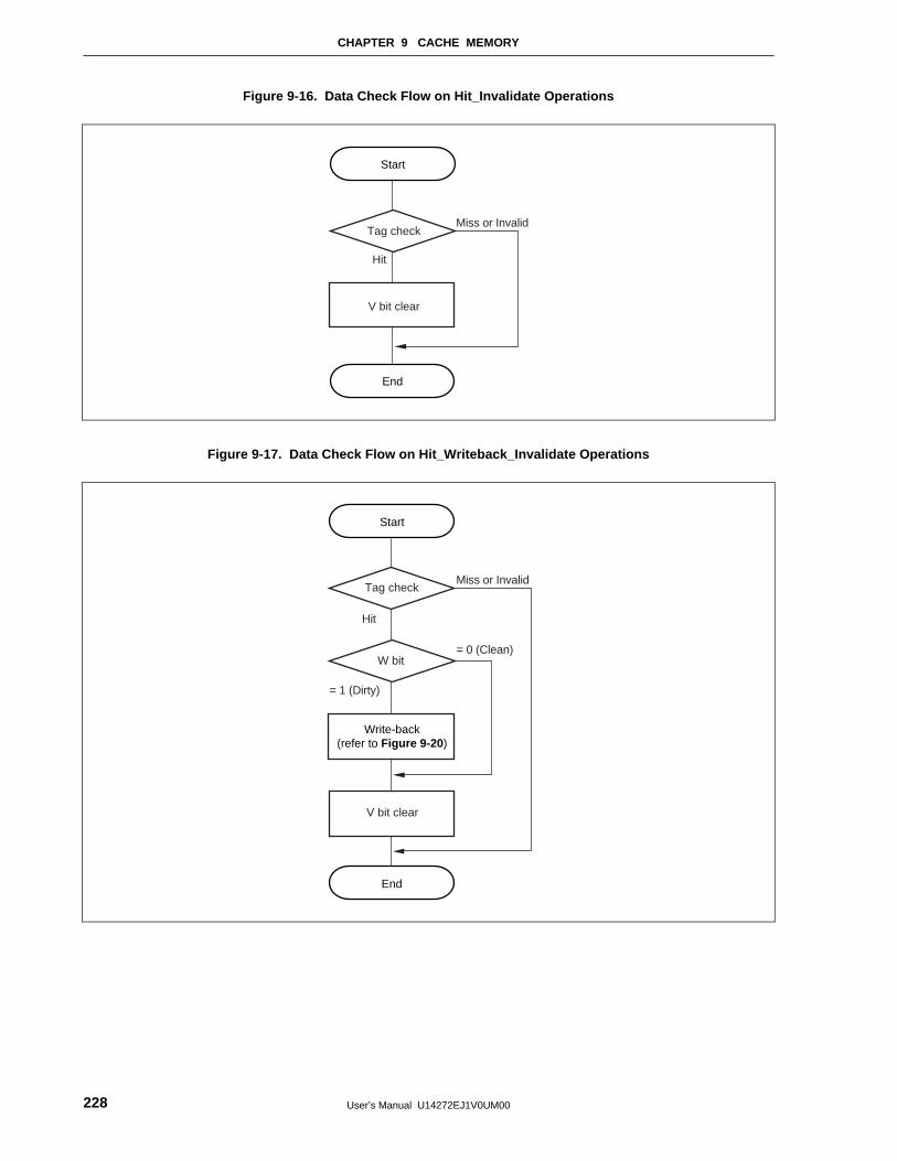
CHAPTER 9 CACHE MEMORY
User’s Manual U14272EJ1V0UM00228
Figure 9-16. Data Check Flow on Hit_Invalidate Operations
Hit
Miss or Invalid
Start
End
V bit clear
Tag check
Figure 9-17. Data Check Flow on Hit_Writeback_Invalidate Operations
Miss or Invalid
Hit
= 0 (Clean)
= 1 (Dirty)
Start
End
W bit
Write-back(refer to Figure 9-20 )
Tag check
V bit clear
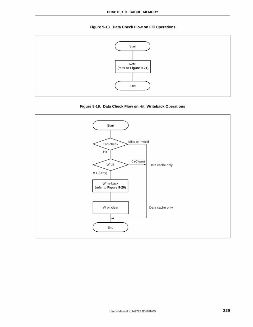
CHAPTER 9 CACHE MEMORY
User’s Manual U14272EJ1V0UM00 229
Figure 9-18. Data Check Flow on Fill Operations
Start
End
Refill (refer to Figure 9-21 )
Figure 9-19. Data Check Flow on Hit_Writeback Operations
Hit
Miss or Invalid
Data cache only
Data cache only
= 0 (Clean)
= 1 (Dirty)
Start
End
W bit
Write-back(refer to Figure 9-20 )
Tag check
W bit clear
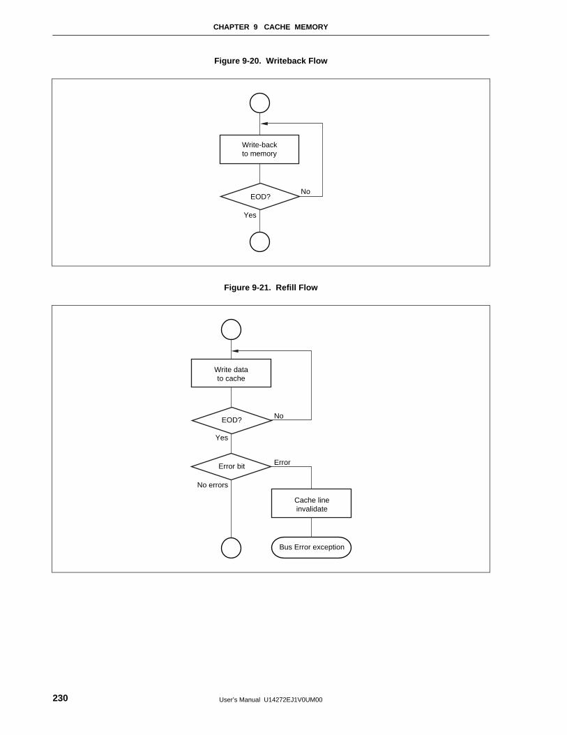
CHAPTER 9 CACHE MEMORY
User’s Manual U14272EJ1V0UM00230
Figure 9-20. Writeback Flow
No
Yes
Write-backto memory
EOD?
Figure 9-21. Refill Flow
Error
No
Yes
No errors
Write datato cache
EOD?
Error bit
Cache lineinvalidate
Bus Error exception
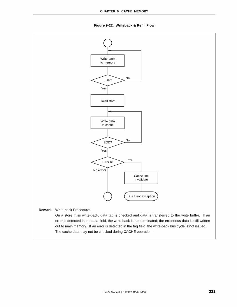
CHAPTER 9 CACHE MEMORY
User’s Manual U14272EJ1V0UM00 231
Figure 9-22. Writeback & Refill Flow
No
Yes
No
Yes
Error
No errors
Write-backto memory
EOD?
Refill start
Error bit
Write datato cache
EOD?
Cache lineinvalidate
Bus Error exception
Remark Write-back Procedure:
On a store miss write-back, data tag is checked and data is transferred to the write buffer. If an
error is detected in the data field, the write back is not terminated; the erroneous data is still written
out to main memory. If an error is detected in the tag field, the write-back bus cycle is not issued.
The cache data may not be checked during CACHE operation.
CHAPTER 9 CACHE MEMORY
User’s Manual U14272EJ1V0UM00232
9.7 Manipulation of the Caches by an External Agent
The VR4181 does not provide any mechanisms for an external agent to examine and manipulate the state and
contents of the caches.
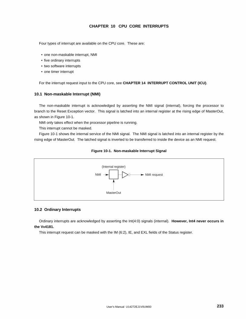
User’s Manual U14272EJ1V0UM00 233
CHAPTER 10 CPU CORE INTERRUPTS
Four types of interrupt are available on the CPU core. These are:
• one non-maskable interrupt, NMI
• five ordinary interrupts
• two software interrupts
• one timer interrupt
For the interrupt request input to the CPU core, see CHAPTER 14 INTERRUPT CONTROL UNIT (ICU) .
10.1 Non-maskable Interrupt (NMI)
The non-maskable interrupt is acknowledged by asserting the NMI signal (internal), forcing the processor to
branch to the Reset Exception vector. This signal is latched into an internal register at the rising edge of MasterOut,
as shown in Figure 10-1.
NMI only takes effect when the processor pipeline is running.
This interrupt cannot be masked.
Figure 10-1 shows the internal service of the NMI signal. The NMI signal is latched into an internal register by the
rising edge of MasterOut. The latched signal is inverted to be transferred to inside the device as an NMI request.
Figure 10-1. Non-maskable Interrupt Signal
NMI requestNMI
MasterOut
(Internal register)
10.2 Ordinary Interrupts
Ordinary interrupts are acknowledged by asserting the Int(4:0) signals (internal). However, Int4 never occurs in
the VR4181.
This interrupt request can be masked with the IM (6:2), IE, and EXL fields of the Status register.
CHAPTER 10 CPU CORE INTERRUPTS
User’s Manual U14272EJ1V0UM00234
10.3 Software Interrupts Generated in CPU Core
Software interrupts generated in the CPU core use bits 1 and 0 of the IP (interrupt pending) field in the Cause
register. These may be written by software, but there is no hardware mechanism to set or clear these bits.
After the processing of a software interrupt exception, corresponding bit of the IP field in the Cause register must
be cleared before returning to ordinary routine or enabling multiple interrupts until the operation returns to normal
routine.
This interrupt request is maskable through the IM (1:0), IE, and EXL fields of the Status register.
10.4 Timer Interrupt
The timer interrupt uses bit 7 of the IP (interrupt pending) field of the Cause register. This bit is set automatically
whenever the value of the Count register equals the value of the Compare register, and an interrupt request is
acknowledged.
This interrupt is maskable through IM7 of the IM field of the Status register.
10.5 Asserting Interrupts
10.5.1 Detecting hardware interrupts
Figure 10-2 shows how the hardware interrupts are readable through the Cause register.
• The timer interrupt signal, IP7, is directly readable as bit 15 of the Cause register.
• Bits 4:0 of the Interrupt register are bit-wise ORed with the current value of the Int(4:0) signals and the result is
directly readable as bits 14:10 of the Cause register.
IP(1:0) of the Cause register, which are described in Chapter 7, are software interrupts. There is no hardware
mechanism for setting or clearing the software interrupts.
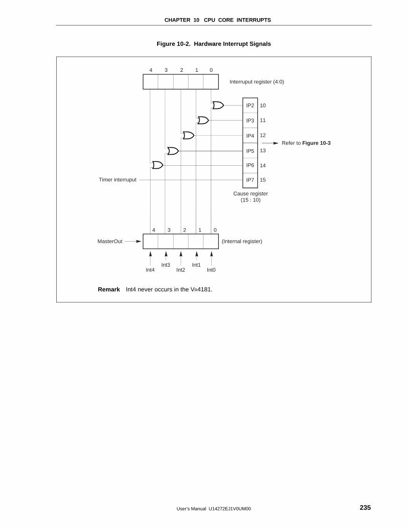
CHAPTER 10 CPU CORE INTERRUPTS
User’s Manual U14272EJ1V0UM00 235
Figure 10-2. Hardware Interrupt Signals
IP2
IP3
IP4
IP5
IP6
4 3 2 1 0
4 3 2 1 0
IP7
Int4Int3
Int2Int1
Int0
10
11
12
13Refer to Figure 10-3
Cause register(15 : 10)
(Internal register)MasterOut
Timer interruput
Interruput register (4:0)
14
15
Remark Int4 never occurs in the VR4181.
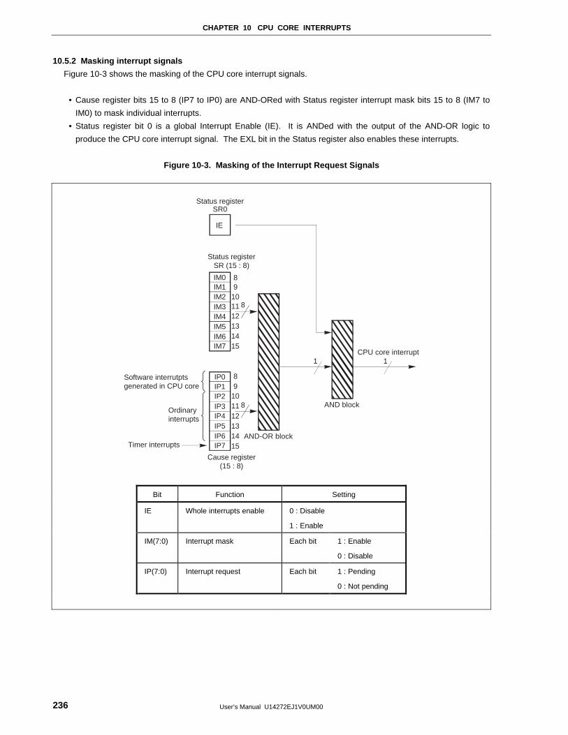
CHAPTER 10 CPU CORE INTERRUPTS
User’s Manual U14272EJ1V0UM00236
10.5.2 Masking interrupt signals
Figure 10-3 shows the masking of the CPU core interrupt signals.
• Cause register bits 15 to 8 (IP7 to IP0) are AND-ORed with Status register interrupt mask bits 15 to 8 (IM7 to
IM0) to mask individual interrupts.
• Status register bit 0 is a global Interrupt Enable (IE). It is ANDed with the output of the AND-OR logic to
produce the CPU core interrupt signal. The EXL bit in the Status register also enables these interrupts.
Figure 10-3. Masking of the Interrupt Request Signals
IM0
IE
Status registerSR0
Software interrutptsgenerated in CPU core
Ordinaryinterrupts
Timer interrupts
IM1IM2IM3IM4IM5IM6IM7
IP0IP1IP2IP3IP4IP5IP6IP7
8
AND-OR block
AND block
1 1CPU core interrupt
8
8
Status registerSR (15 : 8)
Cause register(15 : 8)
9101112131415
89
101112131415
Bit Function Setting
IE Whole interrupts enable 0 : Disable
1 : Enable
IM(7:0) Interrupt mask Each bit 1 : Enable
0 : Disable
IP(7:0) Interrupt request Each bit 1 : Pending
0 : Not pending
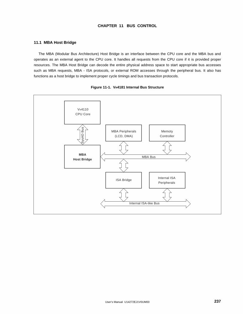
User’s Manual U14272EJ1V0UM00 237
CHAPTER 11 BUS CONTROL
11.1 MBA Host Bridge
The MBA (Modular Bus Architecture) Host Bridge is an interface between the CPU core and the MBA bus and
operates as an external agent to the CPU core. It handles all requests from the CPU core if it is provided proper
resources. The MBA Host Bridge can decode the entire physical address space to start appropriate bus accesses
such as MBA requests, MBA - ISA protocols, or external ROM accesses through the peripheral bus. It also has
functions as a host bridge to implement proper cycle timings and bus transaction protocols.
Figure 11-1. V R4181 Internal Bus Structure
MBA Bus
ISA BridgeInternal ISA
Peripherals
MBA Peripherals
(LCD, DMA)
Memoty
Controller
VR4110
CPU Core
MBA
Host Bridge
Internal ISA-like Bus
Sys
AD
Bu
s
CHAPTER 11 BUS CONTROL
User’s Manual U14272EJ1V0UM00238
11.1.1 MBA Host Bridge ROM and register address space
Physical address Type Device
0x1FFF FFFF to 0x1800 0000 Memory (range) ROM
0x0A00 0014 to 0x0A00 0000 I/O (range) Bus Control registers
0x0A00 0080 I/O Interrupt register
0x0A00 008C I/O Interrupt register
0x0A00 0098 I/O Interrupt register
0x0A00 009A I/O Interrupt register
0x0A00 0200 I/O Interrupt register
0x0A00 0206 I/O Interrupt register
In addition to the decoding of above addresses, the Host Bridge generates MBA select signals if other MBA
masters want to access the above devices. The Host Bridge responds to the above addresses only upon a CPU
access. For any other addresses the Host Bridge initiates an MBA cycle.
11.1.2 MBA modules address space
(1) Memory controller
Physical address Type Device
0x03FF FFFF to 0x0000 0000 Memory (range) DRAM
0x0A0 003FF to 0x0A00 0300 I/O (range) Control registers
The MBA memory controller returns an MBA select signal upon a decoding of the above address ranges.
(2) DMA controller
Physical address Type Device
0x0A00 0048 to 0x0A00 0020 I/O (range) Control registers 1
0x0A00 06FF to 0x0A00 0600 I/O (range) Control registers 2
The MBA DMA controller returns an MBA select signal upon a decoding of the above I/O ranges.
(3) LCD module (LCD Control Unit)
Physical address Type Device
0x0A00 05FF to 0x0000 0400 I/O (Range) Control registers
The LCD module returns an MBA select signal upon a decoding of the above I/O range.
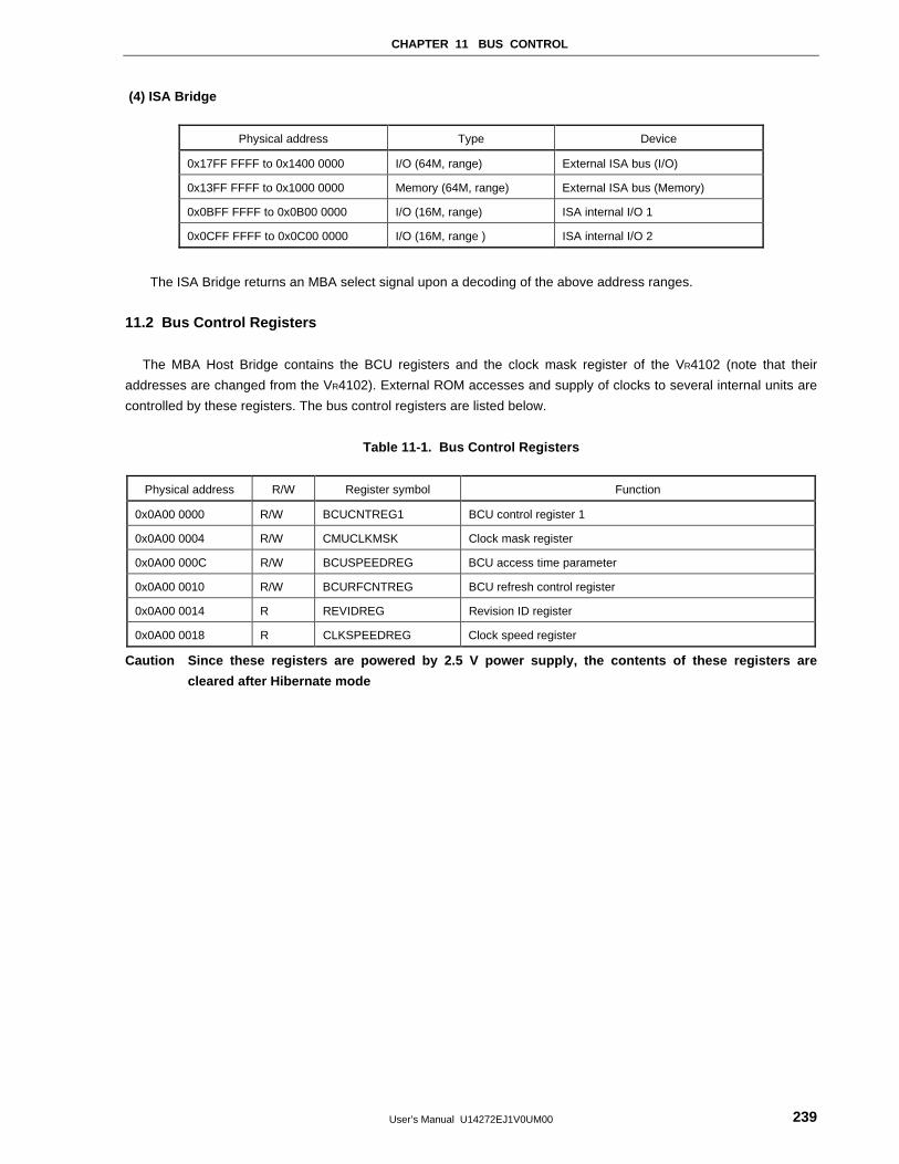
CHAPTER 11 BUS CONTROL
User’s Manual U14272EJ1V0UM00 239
(4) ISA Bridge
Physical address Type Device
0x17FF FFFF to 0x1400 0000 I/O (64M, range) External ISA bus (I/O)
0x13FF FFFF to 0x1000 0000 Memory (64M, range) External ISA bus (Memory)
0x0BFF FFFF to 0x0B00 0000 I/O (16M, range) ISA internal I/O 1
0x0CFF FFFF to 0x0C00 0000 I/O (16M, range ) ISA internal I/O 2
The ISA Bridge returns an MBA select signal upon a decoding of the above address ranges.
11.2 Bus Control Registers
The MBA Host Bridge contains the BCU registers and the clock mask register of the VR4102 (note that their
addresses are changed from the VR4102). External ROM accesses and supply of clocks to several internal units are
controlled by these registers. The bus control registers are listed below.
Table 11-1. Bus Control Registers
Physical address R/W Register symbol Function
0x0A00 0000 R/W BCUCNTREG1 BCU control register 1
0x0A00 0004 R/W CMUCLKMSK Clock mask register
0x0A00 000C R/W BCUSPEEDREG BCU access time parameter
0x0A00 0010 R/W BCURFCNTREG BCU refresh control register
0x0A00 0014 R REVIDREG Revision ID register
0x0A00 0018 R CLKSPEEDREG Clock speed register
Caution Since these registers are powered by 2.5 V power supply, the contents of these registers are
cleared after Hibernate mode
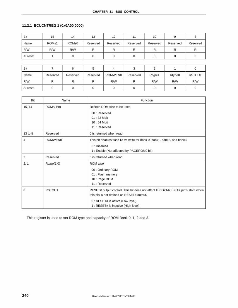
CHAPTER 11 BUS CONTROL
User’s Manual U14272EJ1V0UM00240
11.2.1 BCUCNTREG 1 (0x0A00 0000)
Bit 15 14 13 12 11 10 9 8
Name ROMs1 ROMs0 Reserved Reserved Reserved Reserved Reserved Reserved
R/W R/W R/W R R R R R R
At reset 1 0 0 0 0 0 0 0
Bit 7 6 5 4 3 2 1 0
Name Reserved Reserved Reserved ROMWEN0 Reserved Rtype1 Rtype0 RSTOUT
R/W R R R R/W R R/W R/W R/W
At reset 0 0 0 0 0 0 0 0
Bit Name Function
15, 14 ROMs(1:0) Defines ROM size to be used
00 : Reserved
01 : 32 Mbit
10 : 64 Mbit
11 : Reserved
13 to 5 Reserved 0 is returned when read
4 ROMWEN0 This bit enables flash ROM write for bank 0, bank1, bank2, and bank3
0 : Disabled
1 : Enable (Not affected by PAGEROM0 bit)
3 Reserved 0 is returned when read
2, 1 Rtype(1:0) ROM type
00 : Ordinary ROM
01 : Flash memory
10 : Page ROM
11 : Reserved
0 RSTOUT RESET# output control. This bit does not affect GPIO21/RESET# pin’s state when
this pin is not defined as RESET# output.
0 : RESET# is active (Low level)
1 : RESET# is inactive (High level)
This register is used to set ROM type and capacity of ROM Bank 0, 1, 2 and 3.
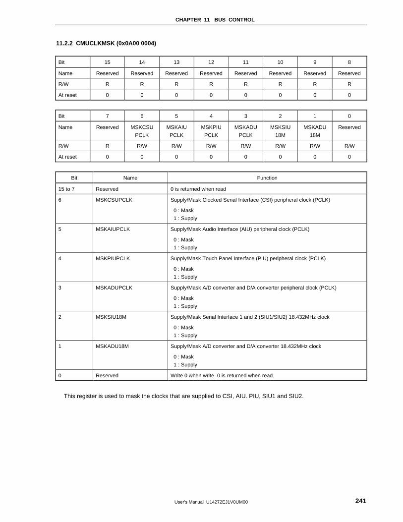
CHAPTER 11 BUS CONTROL
User’s Manual U14272EJ1V0UM00 241
11.2.2 CMUCLKMSK (0x0A00 0004)
Bit 15 14 13 12 11 10 9 8
Name Reserved Reserved Reserved Reserved Reserved Reserved Reserved Reserved
R/W R R R R R R R R
At reset 0 0 0 0 0 0 0 0
Bit 7 6 5 4 3 2 1 0
Name Reserved MSKCSU
PCLK
MSKAIU
PCLK
MSKPIU
PCLK
MSKADU
PCLK
MSKSIU
18M
MSKADU
18M
Reserved
R/W R R/W R/W R/W R/W R/W R/W R/W
At reset 0 0 0 0 0 0 0 0
Bit Name Function
15 to 7 Reserved 0 is returned when read
6 MSKCSUPCLK Supply/Mask Clocked Serial Interface (CSI) peripheral clock (PCLK)
0 : Mask
1 : Supply
5 MSKAIUPCLK Supply/Mask Audio Interface (AIU) peripheral clock (PCLK)
0 : Mask
1 : Supply
4 MSKPIUPCLK Supply/Mask Touch Panel Interface (PIU) peripheral clock (PCLK)
0 : Mask
1 : Supply
3 MSKADUPCLK Supply/Mask A/D converter and D/A converter peripheral clock (PCLK)
0 : Mask
1 : Supply
2 MSKSIU18M Supply/Mask Serial Interface 1 and 2 (SIU1/SIU2) 18.432MHz clock
0 : Mask
1 : Supply
1 MSKADU18M Supply/Mask A/D converter and D/A converter 18.432MHz clock
0 : Mask
1 : Supply
0 Reserved Write 0 when write. 0 is returned when read.
This register is used to mask the clocks that are supplied to CSI, AIU. PIU, SIU1 and SIU2.
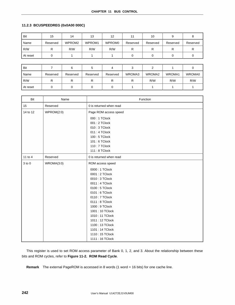
CHAPTER 11 BUS CONTROL
User’s Manual U14272EJ1V0UM00242
11.2.3 BCUSPEEDREG (0x0A00 000C)
Bit 15 14 13 12 11 10 9 8
Name Reserved WPROM2 WPROM1 WPROM0 Reserved Reserved Reserved Reserved
R/W R R/W R/W R/W R R R R
At reset 0 1 1 1 0 0 0 0
Bit 7 6 5 4 3 2 1 0
Name Reserved Reserved Reserved Reserved WROMA3 WROMA2 WROMA1 WROMA0
R/W R R R R R R/W R/W R/W
At reset 0 0 0 0 1 1 1 1
Bit Name Function
15 Reserved 0 is returned when read
14 to 12 WPROM(2:0) Page ROM access speed
000 : 1 TClock
001 : 2 TClock
010 : 3 TClock
011 : 4 TClock
100 : 5 TClock
101 : 6 TClock
110 : 7 TClock
111 : 8 TClock
11 to 4 Reserved 0 is returned when read
3 to 0 WROMA(3:0) ROM access speed
0000 : 1 TClock
0001 : 2 TClock
0010 : 3 TClock
0011 : 4 TClock
0100 : 5 TClock
0101 : 6 TClock
0110 : 7 TClock
0111 : 8 TClock
1000 : 9 TClock
1001 : 10 TClock
1010 : 11 TClock
1011 : 12 TClock
1100 : 13 TClock
1101 : 14 TClock
1110 : 15 TClock
1111 : 16 TClock
This register is used to set ROM access parameter of Bank 0, 1, 2, and 3. About the relationship between these
bits and ROM cycles, refer to Figure 11-2. ROM Read Cycle .
Remark The external PageROM is accessed in 8 words (1 word = 16 bits) for one cache line.
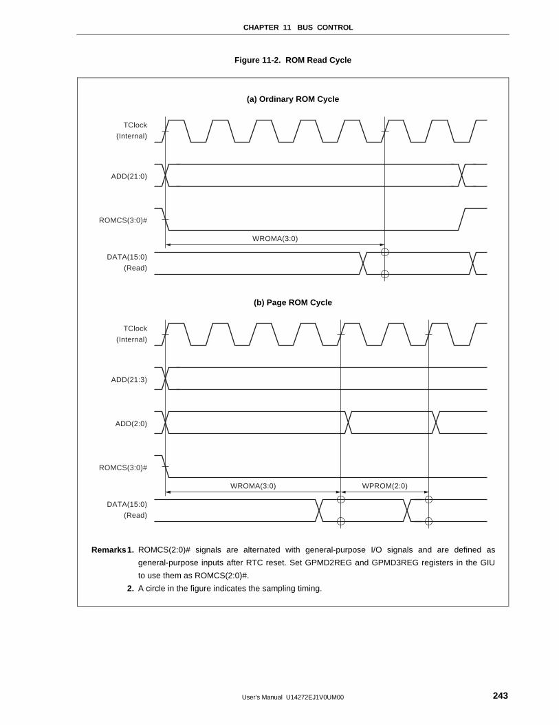
CHAPTER 11 BUS CONTROL
User’s Manual U14272EJ1V0UM00 243
Figure 11-2. ROM Read Cycle
(a) Ordinary ROM Cycle
TClock
(Internal)
ADD(21:0)
DATA(15:0)
(Read)
ROMCS(3:0)#
WROMA(3:0)
(b) Page ROM Cycle
WROMA(3:0)
ADD(2:0)
TClock
(Internal)
ADD(21:3)
DATA(15:0)
(Read)
ROMCS(3:0)#
WPROM(2:0)
Remarks1. ROMCS(2:0)# signals are alternated with general-purpose I/O signals and are defined as
general-purpose inputs after RTC reset. Set GPMD2REG and GPMD3REG registers in the GIU
to use them as ROMCS(2:0)#.
2. A circle in the figure indicates the sampling timing.
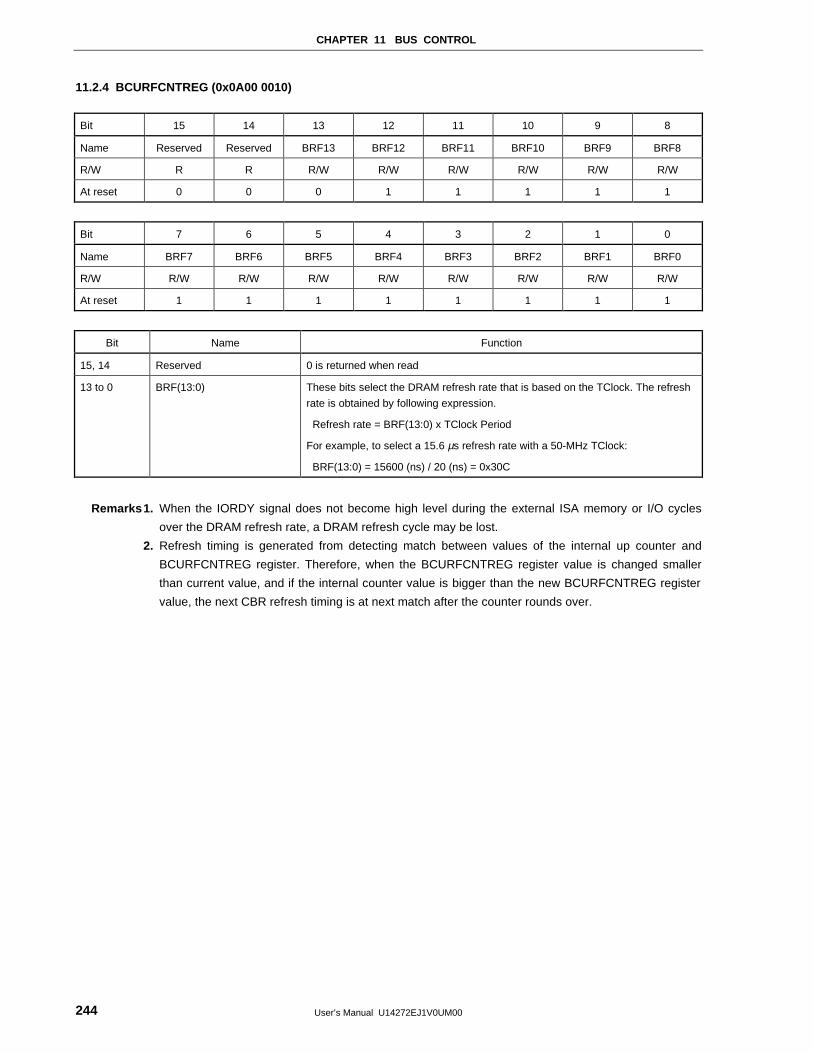
CHAPTER 11 BUS CONTROL
User’s Manual U14272EJ1V0UM00244
11.2.4 BCURFCNTREG (0x0A00 0010)
Bit 15 14 13 12 11 10 9 8
Name Reserved Reserved BRF13 BRF12 BRF11 BRF10 BRF9 BRF8
R/W R R R/W R/W R/W R/W R/W R/W
At reset 0 0 0 1 1 1 1 1
Bit 7 6 5 4 3 2 1 0
Name BRF7 BRF6 BRF5 BRF4 BRF3 BRF2 BRF1 BRF0
R/W R/W R/W R/W R/W R/W R/W R/W R/W
At reset 1 1 1 1 1 1 1 1
Bit Name Function
15, 14 Reserved 0 is returned when read
13 to 0 BRF(13:0) These bits select the DRAM refresh rate that is based on the TClock. The refresh
rate is obtained by following expression.
Refresh rate = BRF(13:0) x TClock Period
For example, to select a 15.6 µs refresh rate with a 50-MHz TClock:
BRF(13:0) = 15600 (ns) / 20 (ns) = 0x30C
Remarks1. When the IORDY signal does not become high level during the external ISA memory or I/O cycles
over the DRAM refresh rate, a DRAM refresh cycle may be lost.
2. Refresh timing is generated from detecting match between values of the internal up counter and
BCURFCNTREG register. Therefore, when the BCURFCNTREG register value is changed smaller
than current value, and if the internal counter value is bigger than the new BCURFCNTREG register
value, the next CBR refresh timing is at next match after the counter rounds over.
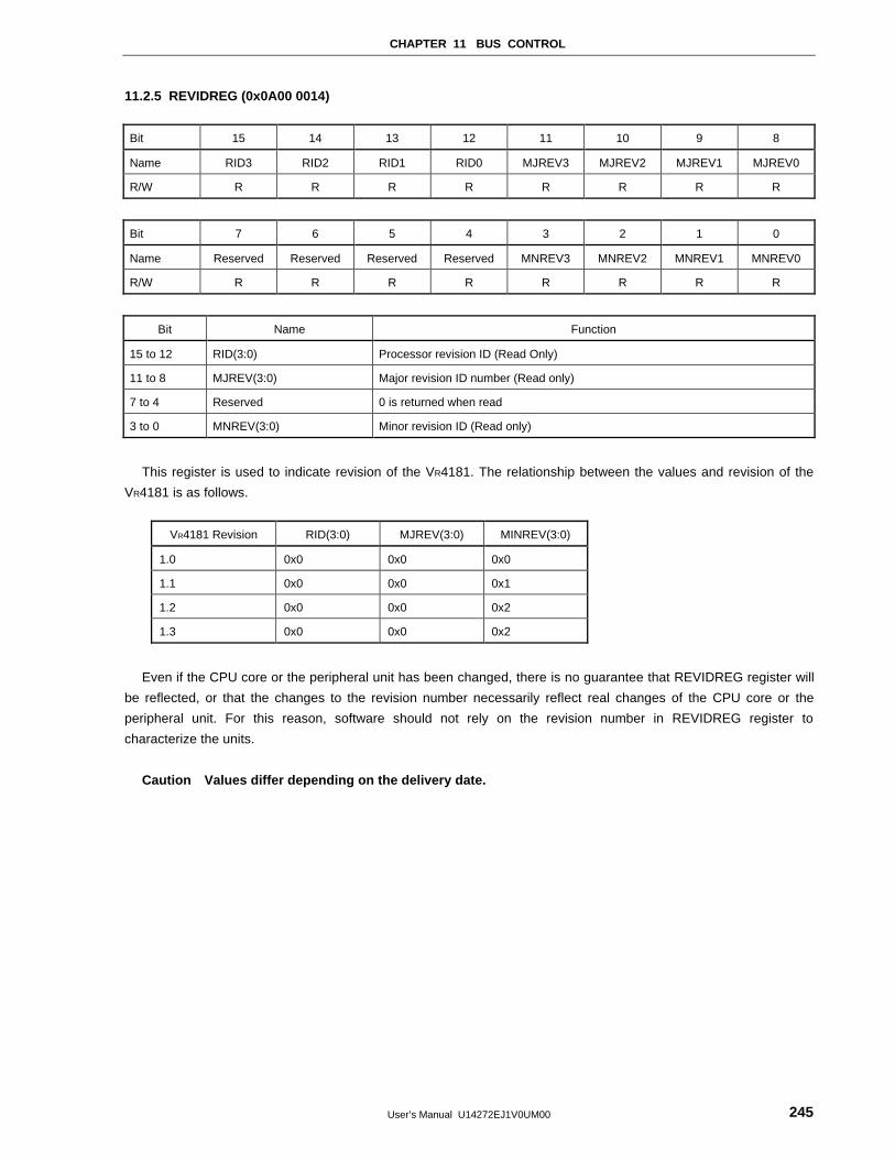
CHAPTER 11 BUS CONTROL
User’s Manual U14272EJ1V0UM00 245
11.2.5 REVIDREG (0x0A00 0014)
Bit 15 14 13 12 11 10 9 8
Name RID3 RID2 RID1 RID0 MJREV3 MJREV2 MJREV1 MJREV0
R/W R R R R R R R R
Bit 7 6 5 4 3 2 1 0
Name Reserved Reserved Reserved Reserved MNREV3 MNREV2 MNREV1 MNREV0
R/W R R R R R R R R
Bit Name Function
15 to 12 RID(3:0) Processor revision ID (Read Only)
11 to 8 MJREV(3:0) Major revision ID number (Read only)
7 to 4 Reserved 0 is returned when read
3 to 0 MNREV(3:0) Minor revision ID (Read only)
This register is used to indicate revision of the VR4181. The relationship between the values and revision of the
VR4181 is as follows.
VR4181 Revision RID(3:0) MJREV(3:0) MINREV(3:0)
1.0 0x0 0x0 0x0
1.1 0x0 0x0 0x1
1.2 0x0 0x0 0x2
1.3 0x0 0x0 0x2
Even if the CPU core or the peripheral unit has been changed, there is no guarantee that REVIDREG register will
be reflected, or that the changes to the revision number necessarily reflect real changes of the CPU core or the
peripheral unit. For this reason, software should not rely on the revision number in REVIDREG register to
characterize the units.
Caution Values differ depending on the delivery date.
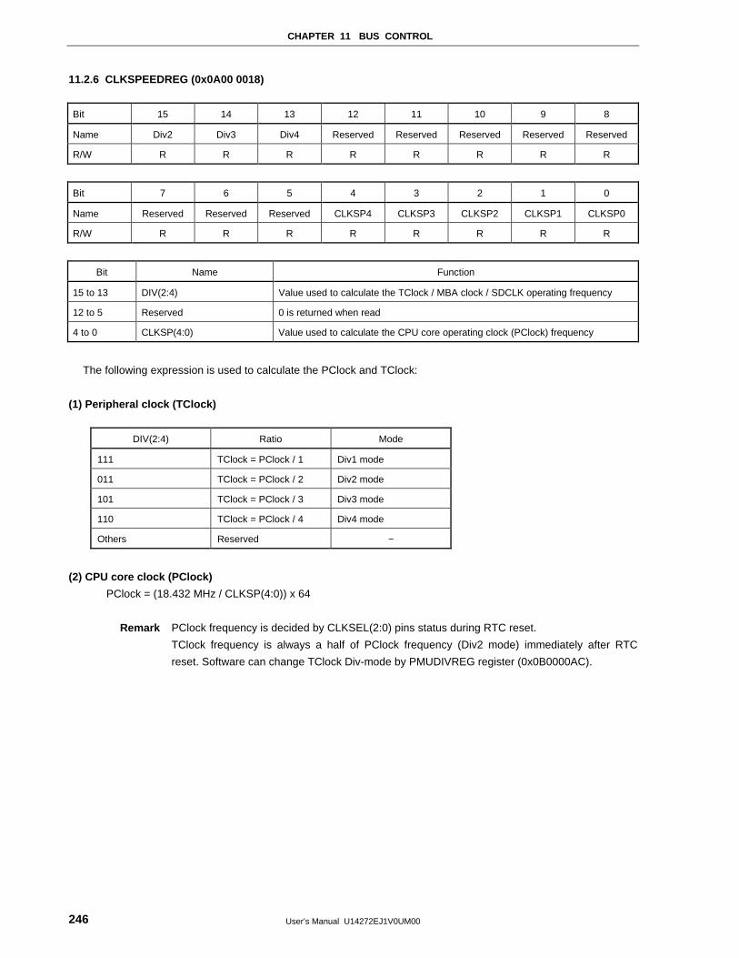
CHAPTER 11 BUS CONTROL
User’s Manual U14272EJ1V0UM00246
11.2.6 CLKSPEEDREG (0x0A00 0018)
Bit 15 14 13 12 11 10 9 8
Name Div2 Div3 Div4 Reserved Reserved Reserved Reserved Reserved
R/W R R R R R R R R
Bit 7 6 5 4 3 2 1 0
Name Reserved Reserved Reserved CLKSP4 CLKSP3 CLKSP2 CLKSP1 CLKSP0
R/W R R R R R R R R
Bit Name Function
15 to 13 DIV(2:4) Value used to calculate the TClock / MBA clock / SDCLK operating frequency
12 to 5 Reserved 0 is returned when read
4 to 0 CLKSP(4:0) Value used to calculate the CPU core operating clock (PClock) frequency
The following expression is used to calculate the PClock and TClock:
(1) Peripheral clock (TClock)
DIV(2:4) Ratio Mode
111 TClock = PClock / 1 Div1 mode
011 TClock = PClock / 2 Div2 mode
101 TClock = PClock / 3 Div3 mode
110 TClock = PClock / 4 Div4 mode
Others Reserved −
(2) CPU core clock (PClock)
PClock = (18.432 MHz / CLKSP(4:0)) x 64
Remark PClock frequency is decided by CLKSEL(2:0) pins status during RTC reset.
TClock frequency is always a half of PClock frequency (Div2 mode) immediately after RTC
reset. Software can change TClock Div-mode by PMUDIVREG register (0x0B0000AC).
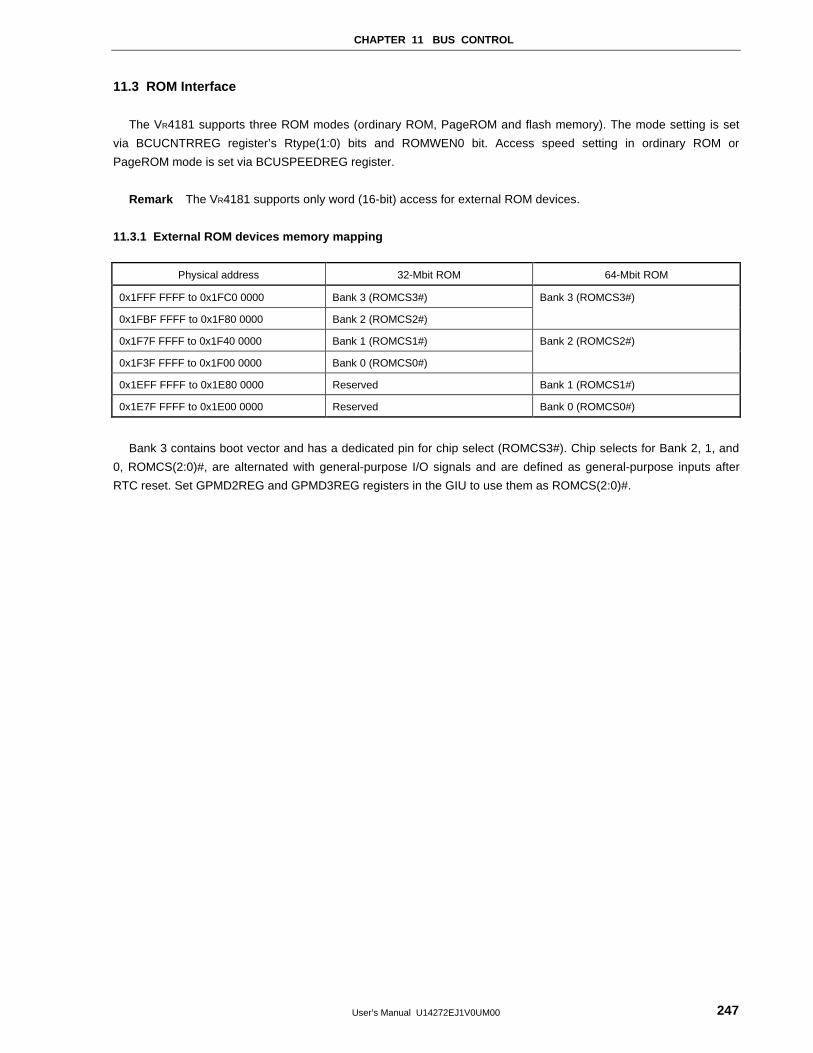
CHAPTER 11 BUS CONTROL
User’s Manual U14272EJ1V0UM00 247
11.3 ROM Interface
The VR4181 supports three ROM modes (ordinary ROM, PageROM and flash memory). The mode setting is set
via BCUCNTRREG register’s Rtype(1:0) bits and ROMWEN0 bit. Access speed setting in ordinary ROM or
PageROM mode is set via BCUSPEEDREG register.
Remark The VR4181 supports only word (16-bit) access for external ROM devices.
11.3.1 External ROM devices memory mapping
Physical address 32-Mbit ROM 64-Mbit ROM
0x1FFF FFFF to 0x1FC0 0000 Bank 3 (ROMCS3#) Bank 3 (ROMCS3#)
0x1FBF FFFF to 0x1F80 0000 Bank 2 (ROMCS2#)
0x1F7F FFFF to 0x1F40 0000 Bank 1 (ROMCS1#) Bank 2 (ROMCS2#)
0x1F3F FFFF to 0x1F00 0000 Bank 0 (ROMCS0#)
0x1EFF FFFF to 0x1E80 0000 Reserved Bank 1 (ROMCS1#)
0x1E7F FFFF to 0x1E00 0000 Reserved Bank 0 (ROMCS0#)
Bank 3 contains boot vector and has a dedicated pin for chip select (ROMCS3#). Chip selects for Bank 2, 1, and
0, ROMCS(2:0)#, are alternated with general-purpose I/O signals and are defined as general-purpose inputs after
RTC reset. Set GPMD2REG and GPMD3REG registers in the GIU to use them as ROMCS(2:0)#.
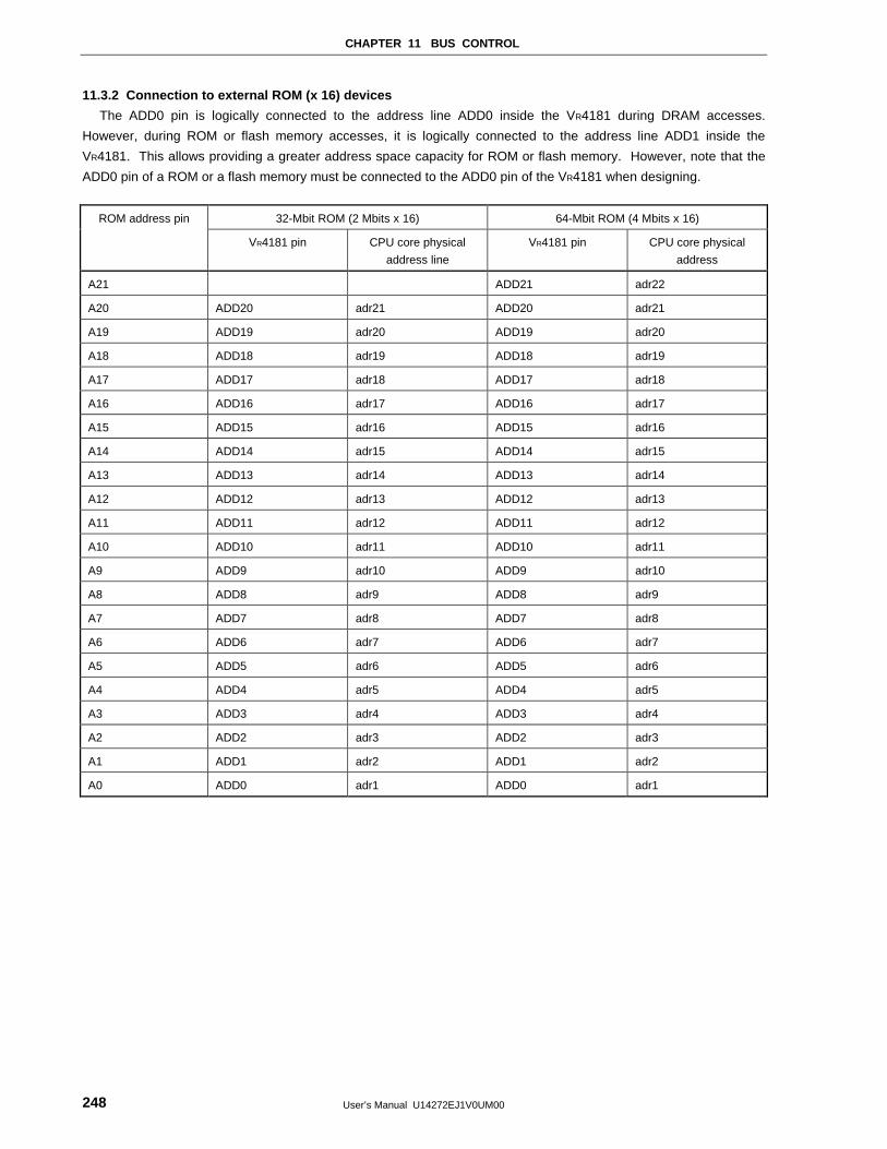
CHAPTER 11 BUS CONTROL
User’s Manual U14272EJ1V0UM00248
11.3.2 Connection to external ROM (x 16) devices
The ADD0 pin is logically connected to the address line ADD0 inside the VR4181 during DRAM accesses.
However, during ROM or flash memory accesses, it is logically connected to the address line ADD1 inside the
VR4181. This allows providing a greater address space capacity for ROM or flash memory. However, note that the
ADD0 pin of a ROM or a flash memory must be connected to the ADD0 pin of the VR4181 when designing.
ROM address pin 32-Mbit ROM (2 Mbits x 16) 64-Mbit ROM (4 Mbits x 16)
VR4181 pin CPU core physical
address line
VR4181 pin CPU core physical
address
A21 ADD21 adr22
A20 ADD20 adr21 ADD20 adr21
A19 ADD19 adr20 ADD19 adr20
A18 ADD18 adr19 ADD18 adr19
A17 ADD17 adr18 ADD17 adr18
A16 ADD16 adr17 ADD16 adr17
A15 ADD15 adr16 ADD15 adr16
A14 ADD14 adr15 ADD14 adr15
A13 ADD13 adr14 ADD13 adr14
A12 ADD12 adr13 ADD12 adr13
A11 ADD11 adr12 ADD11 adr12
A10 ADD10 adr11 ADD10 adr11
A9 ADD9 adr10 ADD9 adr10
A8 ADD8 adr9 ADD8 adr9
A7 ADD7 adr8 ADD7 adr8
A6 ADD6 adr7 ADD6 adr7
A5 ADD5 adr6 ADD5 adr6
A4 ADD4 adr5 ADD4 adr5
A3 ADD3 adr4 ADD3 adr4
A2 ADD2 adr3 ADD2 adr3
A1 ADD1 adr2 ADD1 adr2
A0 ADD0 adr1 ADD0 adr1
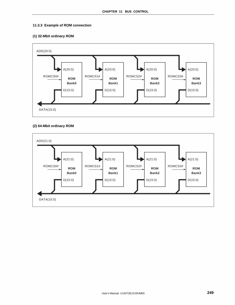
CHAPTER 11 BUS CONTROL
User’s Manual U14272EJ1V0UM00 249
11.3.3 Example of ROM connection
(1) 32-Mbit ordinary ROM
A(20:0)
D(15:0)
A(20:0)
ROMCS0#ROM
Bank1
ROM
Bank0
ADD(20:0)
ROMCS2#ROMCS1#
DATA(15:0)
ROM
Bank3
ROM
Bank2
ROMCS3#
A(20:0) A(20:0)
D(15:0) D(15:0) D(15:0)
(2) 64-Mbit ordinary ROM
A(21:0)
D(15:0)
A(21:0)
ROMCS0#ROM
Bank1
ROM
Bank0
ADD(21:0)
ROMCS2#ROMCS1#
DATA(15:0)
ROM
Bank3
ROM
Bank2
ROMCS3#
A(21:0) A(21:0)
D(15:0) D(15:0) D(15:0)
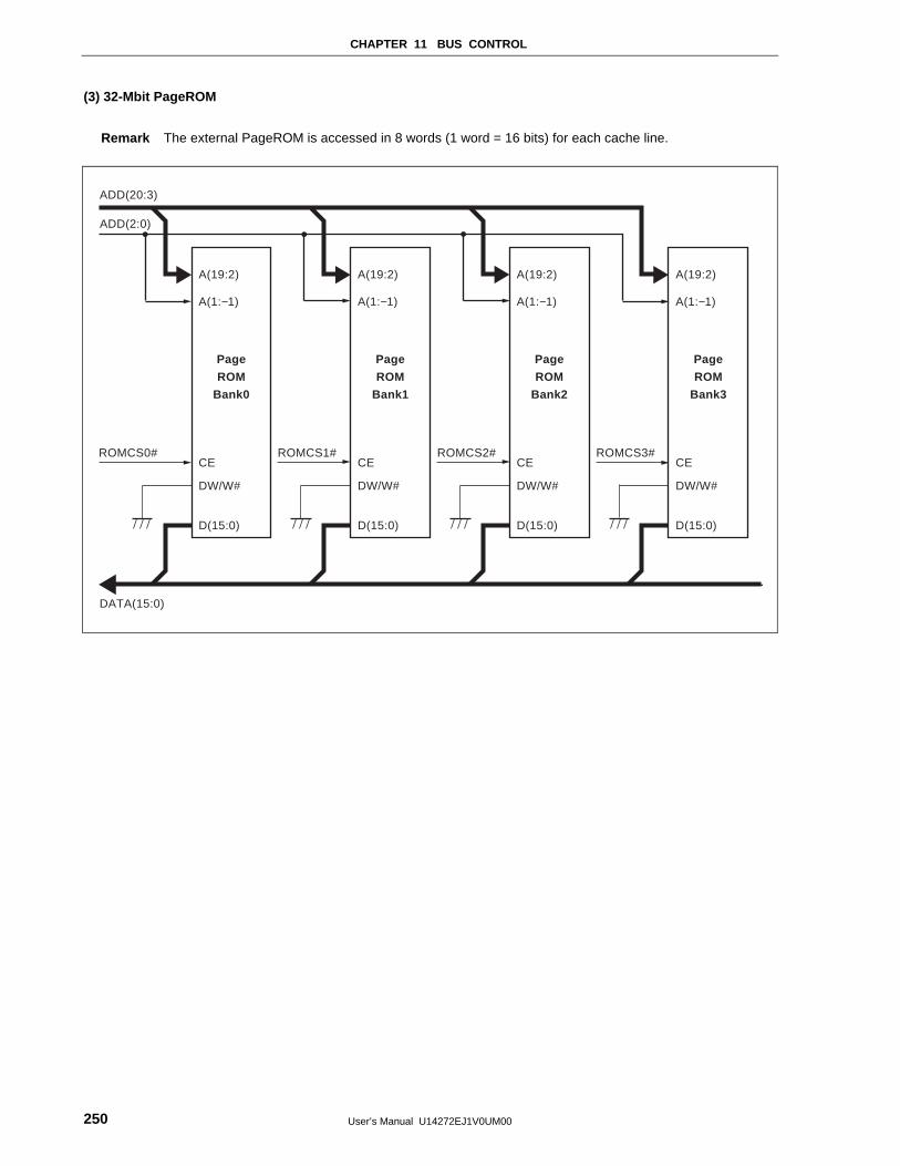
CHAPTER 11 BUS CONTROL
User’s Manual U14272EJ1V0UM00250
(3) 32-Mbit PageROM
Remark The external PageROM is accessed in 8 words (1 word = 16 bits) for each cache line.
CE CE CE CE
A(1:−1)
DW/W#
A(19:2)
ROMCS0#
A(19:2)
D(15:0)
A(19:2)
Page
ROM
Bank1
Page
ROM
Bank0
ADD(20:3)
ROMCS2#ROMCS1#
DATA(15:0)
Page
ROM
Bank3
Page
ROM
Bank2
ROMCS3#
A(19:2)
A(1:−1)
D(15:0) D(15:0) D(15:0)
A(1:−1) A(1:−1)
DW/W# DW/W# DW/W#
ADD(2:0)
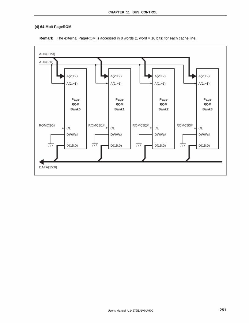
CHAPTER 11 BUS CONTROL
User’s Manual U14272EJ1V0UM00 251
(4) 64-Mbit PageROM
Remark The external PageROM is accessed in 8 words (1 word = 16 bits) for each cache line.
CE CE CE CE
A(1:−1)
DW/W#
A(20:2)
ROMCS0#
A(20:2)
D(15:0)
A(20:2)
Page
ROM
Bank1
Page
ROM
Bank0
ADD(21:3)
ROMCS2#ROMCS1#
DATA(15:0)
Page
ROM
Bank3
Page
ROM
Bank2
ROMCS3#
A(20:2)
A(1:−1)
D(15:0) D(15:0) D(15:0)
A(1:−1) A(1:−1)
DW/W# DW/W# DW/W#
ADD(2:0)
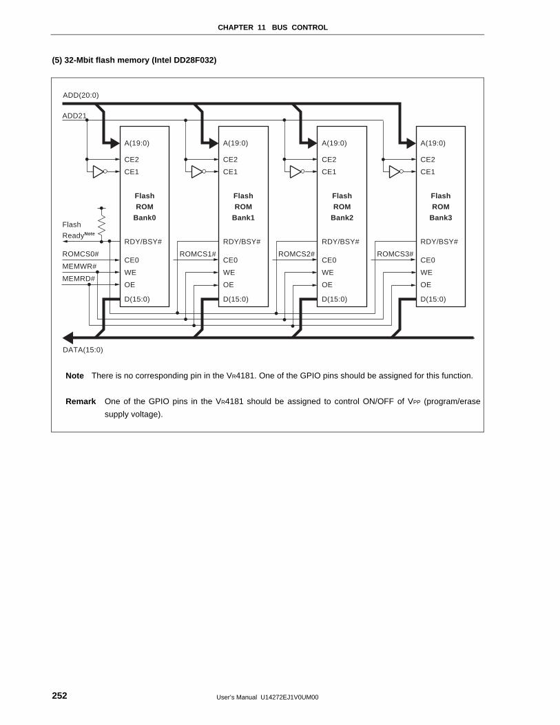
CHAPTER 11 BUS CONTROL
User’s Manual U14272EJ1V0UM00252
(5) 32-Mbit flash memory (Intel DD28F032)
RDY/BSY# RDY/BSY# RDY/BSY#
ROMCS2#ROMCS0# ROMCS3# CE0
CE2
A(19:0)
OE
WEMEMRD#
MEMWR#
ROMCS1#
A(19:0)
D(15:0)
A(19:0)
Flash
ROM
Bank1
Flash
ROM
Bank0
ADD(20:0)
DATA(15:0)
Flash
ROM
Bank3
Flash
ROM
Bank2
A(19:0)
CE0
D(15:0) D(15:0) D(15:0)
OE
WE
CE0
OE
WE
CE0
OE
WE
CE1
CE2
CE1
CE2
CE1
CE2
CE1
RDY/BSY#
Flash
ReadyNote
ADD21
Note There is no corresponding pin in the VR4181. One of the GPIO pins should be assigned for this function.
Remark One of the GPIO pins in the VR4181 should be assigned to control ON/OFF of VPP (program/erase
supply voltage).
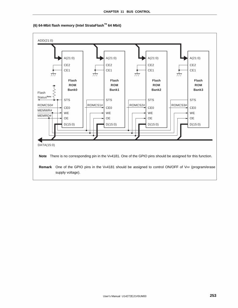
CHAPTER 11 BUS CONTROL
User’s Manual U14272EJ1V0UM00 253
(6) 64-Mbit flash memory (Intel StrataFlash TM 64 Mbit)
STS STS STS
CE0
CE2
A(21:0)
OE
WEMEMRD#
MEMWR#
ROMCS0#
A(21:0)
D(15:0)
A(21:0)
Flash
ROM
Bank1
Flash
ROM
Bank0
ADD(21:0)
ROMCS2#ROMCS1#
DATA(15:0)
Flash
ROM
Bank3
Flash
ROM
Bank2
ROMCS3#
A(21:0)
CE0
D(15:0) D(15:0) D(15:0)
OE
WE
CE0
OE
WE
CE0
OE
WE
CE1
CE2
CE1
CE2
CE1
CE2
CE1
STS
Flash
StatusNote
Note There is no corresponding pin in the VR4181. One of the GPIO pins should be assigned for this function.
Remark One of the GPIO pins in the VR4181 should be assigned to control ON/OFF of VPP (program/erase
supply voltage).
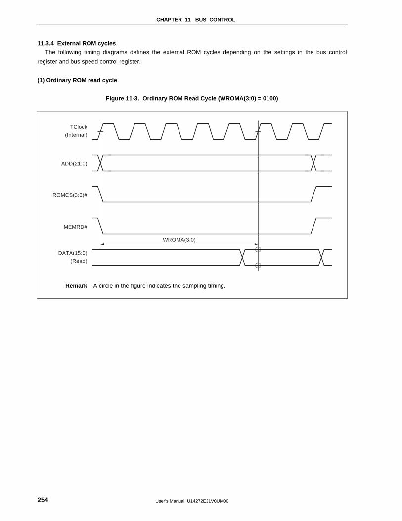
CHAPTER 11 BUS CONTROL
User’s Manual U14272EJ1V0UM00254
11.3.4 External ROM cycles
The following timing diagrams defines the external ROM cycles depending on the settings in the bus control
register and bus speed control register.
(1) Ordinary ROM read cycle
Figure 11-3. Ordinary ROM Read Cycle (WROMA(3:0) = 0100)
TClock
(Internal)
ADD(21:0)
MEMRD#
DATA(15:0)
(Read)
ROMCS(3:0)#
WROMA(3:0)
Remark A circle in the figure indicates the sampling timing.
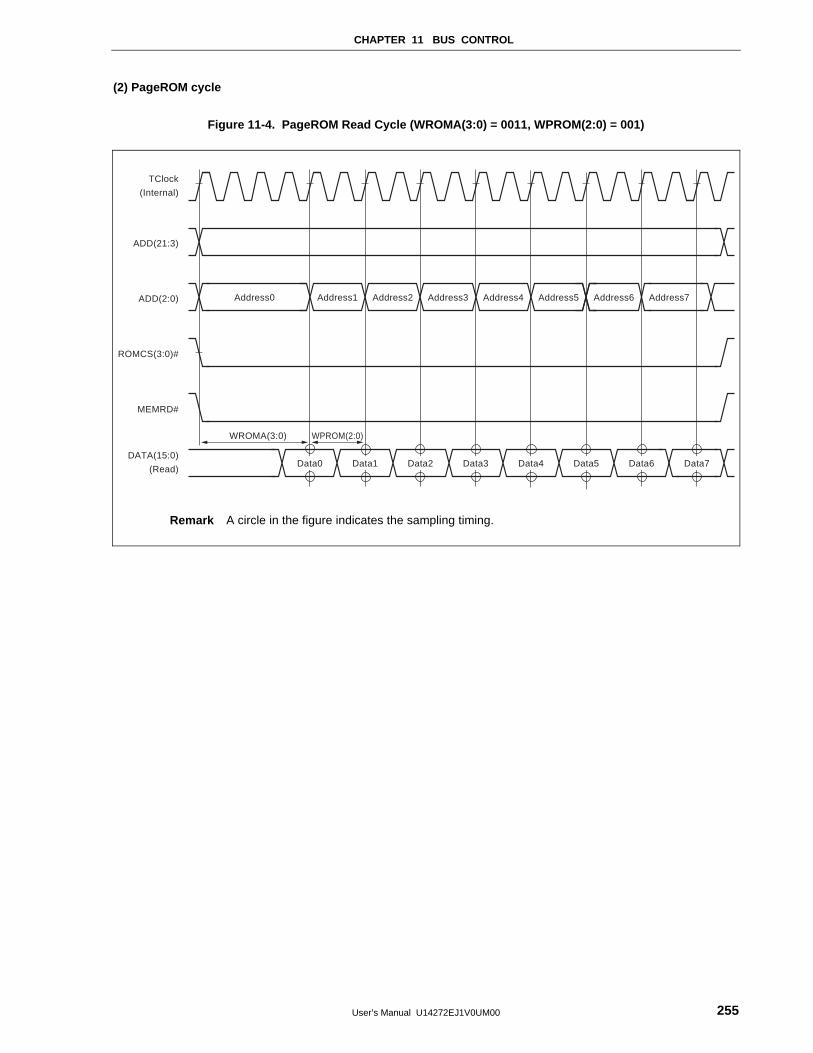
CHAPTER 11 BUS CONTROL
User’s Manual U14272EJ1V0UM00 255
(2) PageROM cycle
Figure 11-4. PageROM Read Cycle (WROMA(3:0) = 0011, WPROM(2:0) = 001)
Address0
ADD(21:3)
TClock
(Internal)
ADD(2:0)
MEMRD#
DATA(15:0)
(Read)
ROMCS(3:0)#
WROMA(3:0) WPROM(2:0)
Address1 Address2 Address3 Address4 Address5 Address6 Address7
Data1 Data4Data3Data2 Data6Data5 Data7Data0
Remark A circle in the figure indicates the sampling timing.
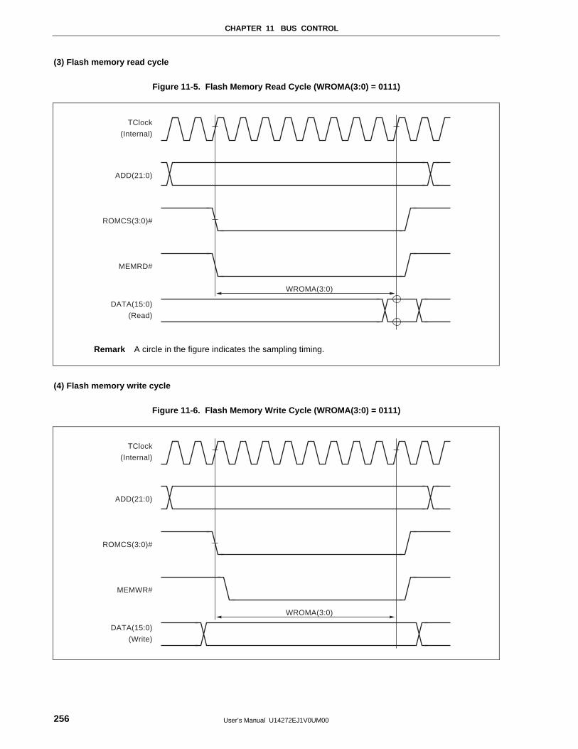
CHAPTER 11 BUS CONTROL
User’s Manual U14272EJ1V0UM00256
(3) Flash memory read cycle
Figure 11-5. Flash Memory Read Cycle (WROMA(3:0) = 0111)
ADD(21:0)
TClock
(Internal)
MEMRD#
DATA(15:0)
(Read)
ROMCS(3:0)#
WROMA(3:0)
Remark A circle in the figure indicates the sampling timing.
(4) Flash memory write cycle
Figure 11-6. Flash Memory Write Cycle (WROMA(3:0) = 0111)
ADD(21:0)
TClock
(Internal)
MEMWR#
DATA(15:0)
(Write)
ROMCS(3:0)#
WROMA(3:0)
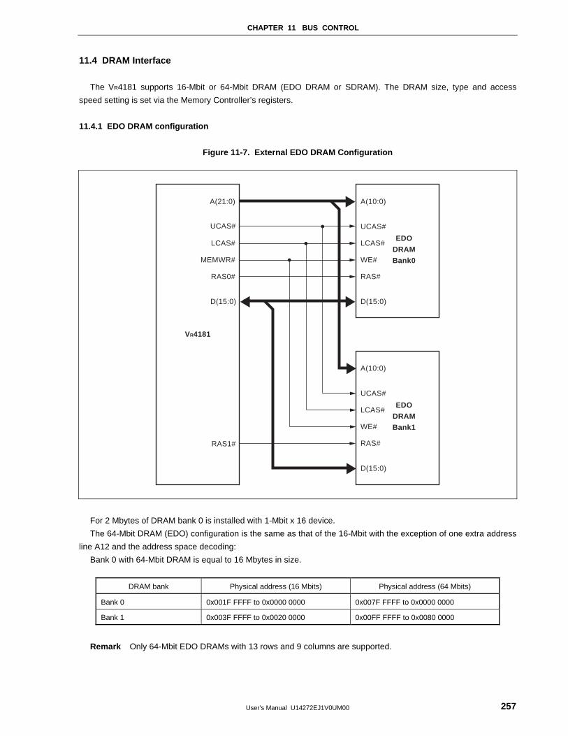
CHAPTER 11 BUS CONTROL
User’s Manual U14272EJ1V0UM00 257
11.4 DRAM Interface
The VR4181 supports 16-Mbit or 64-Mbit DRAM (EDO DRAM or SDRAM). The DRAM size, type and access
speed setting is set via the Memory Controller’s registers.
11.4.1 EDO DRAM configuration
Figure 11-7. External EDO DRAM Configuration
WE#
EDO
DRAM
Bank1
A(10:0)
D(15:0)
RAS#
UCAS#
LCAS#
MEMWR# WE#
RAS0#
UCAS#
A(21:0)
D(15:0)
VR4181
EDO
DRAM
Bank0
A(10:0)
D(15:0)
RAS#
RAS1#
LCAS#
UCAS#
LCAS#
For 2 Mbytes of DRAM bank 0 is installed with 1-Mbit x 16 device.
The 64-Mbit DRAM (EDO) configuration is the same as that of the 16-Mbit with the exception of one extra address
line A12 and the address space decoding:
Bank 0 with 64-Mbit DRAM is equal to 16 Mbytes in size.
DRAM bank Physical address (16 Mbits) Physical address (64 Mbits)
Bank 0 0x001F FFFF to 0x0000 0000 0x007F FFFF to 0x0000 0000
Bank 1 0x003F FFFF to 0x0020 0000 0x00FF FFFF to 0x0080 0000
Remark Only 64-Mbit EDO DRAMs with 13 rows and 9 columns are supported.
CHAPTER 11 BUS CONTROL
User’s Manual U14272EJ1V0UM00258
11.4.2 Mix memory mode (EDO DRAM only)
The memory configuration register provides two bits each for Bank 0 and Bank 1 to set types of DRAMs to be
used. This allows the two banks to be configured with different types of DRAMs, for example, Bank 0 can be mapped
on 64-Mbit devices and Bank 1 on 16-Mbit devices, to optimize the cost of the total memory required.
Table 11-2. VR4181 EDO DRAM Capacity
Bank 0 Bank 1 Total DRAM capacity
16 Mbits 0 2 MB
16 Mbits 16 Mbits 4 MB
64 Mbits 0 8 MB
64 Mbits 16 Mbits 10 MB
64 Mbits 64 Mbits 16 MB
11.4.3 EDO DRAM timing parameters
The following table shows an example of EDO DRAM timing parameters when using -60 devices. These
parameters are set in EDOMCTYREG register.
TClock
frequency
RAS to CAS
delay
CAS pulse
width
CAS precharge RAS precharge RAS pulse
width
Self refresh
RAS precharge
66 MHz 3 TClock 1 TClock 1 TClock 3 TClock 3 TClock 8 TClock
50 MHz 2 TClock 1 TClock 1 TClock 2 TClock 3 TClock 6 TClock
33 MHz 2 TClock 1/2 TClock 1/2 TClock 2 TClock 2 TClock 4 TClock
25 MHz 2 TClock 1/2 TClock 1/2 TClock 1 TClock 2 TClock 3 TClock
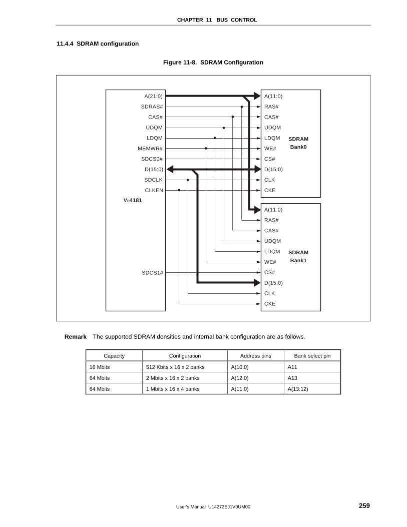
CHAPTER 11 BUS CONTROL
User’s Manual U14272EJ1V0UM00 259
11.4.4 SDRAM configuration
Figure 11-8. SDRAM Configuration
LDQM
LDQM LDQM
D(15:0)
CS#
UDQM
WE#
A(11:0)
CKE
CLK
RAS#
CAS#
SDCS0#
D(15:0) D(15:0)
CS#
UDQM UDQM
SDRAM
Bank1
MEMWR# WE#
SDCLK
SDRAS#
A(21:0)
CLKEN
VR4181
SDRAM
Bank0
A(11:0)
CKE
CLK
SDCS1#
CAS#
RAS#
CAS#
Remark The supported SDRAM densities and internal bank configuration are as follows.
Capacity Configuration Address pins Bank select pin
16 Mbits 512 Kbits x 16 x 2 banks A(10:0) A11
64 Mbits 2 Mbits x 16 x 2 banks A(12:0) A13
64 Mbits 1 Mbits x 16 x 4 banks A(11:0) A(13:12)
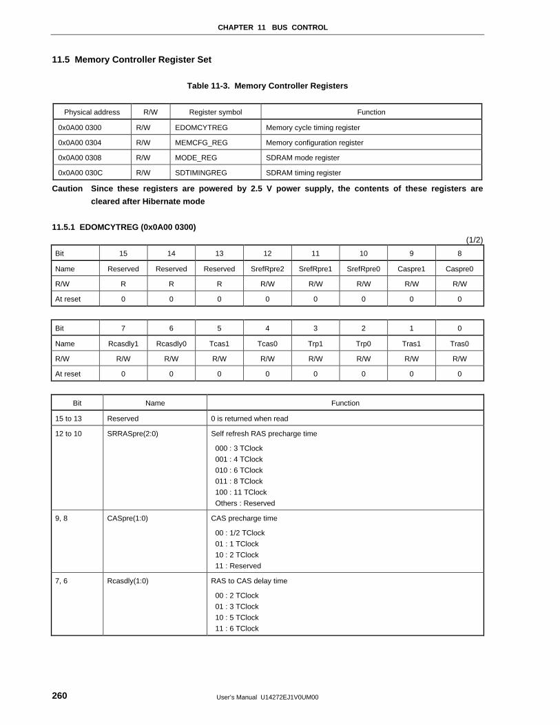
CHAPTER 11 BUS CONTROL
User’s Manual U14272EJ1V0UM00260
11.5 Memory Controller Register Set
Table 11-3. Memory Controller Registers
Physical address R/W Register symbol Function
0x0A00 0300 R/W EDOMCYTREG Memory cycle timing register
0x0A00 0304 R/W MEMCFG_REG Memory configuration register
0x0A00 0308 R/W MODE_REG SDRAM mode register
0x0A00 030C R/W SDTIMINGREG SDRAM timing register
Caution Since these registers are powered by 2.5 V power supply, the contents of these registers are
cleared after Hibernate mode
11.5.1 EDOMCYTREG (0x0A00 0300)
(1/2)
Bit 15 14 13 12 11 10 9 8
Name Reserved Reserved Reserved SrefRpre2 SrefRpre1 SrefRpre0 Caspre1 Caspre0
R/W R R R R/W R/W R/W R/W R/W
At reset 0 0 0 0 0 0 0 0
Bit 7 6 5 4 3 2 1 0
Name Rcasdly1 Rcasdly0 Tcas1 Tcas0 Trp1 Trp0 Tras1 Tras0
R/W R/W R/W R/W R/W R/W R/W R/W R/W
At reset 0 0 0 0 0 0 0 0
Bit Name Function
15 to 13 Reserved 0 is returned when read
12 to 10 SRRASpre(2:0) Self refresh RAS precharge time
000 : 3 TClock
001 : 4 TClock
010 : 6 TClock
011 : 8 TClock
100 : 11 TClock
Others : Reserved
9, 8 CASpre(1:0) CAS precharge time
00 : 1/2 TClock
01 : 1 TClock
10 : 2 TClock
11 : Reserved
7, 6 Rcasdly(1:0) RAS to CAS delay time
00 : 2 TClock
01 : 3 TClock
10 : 5 TClock
11 : 6 TClock
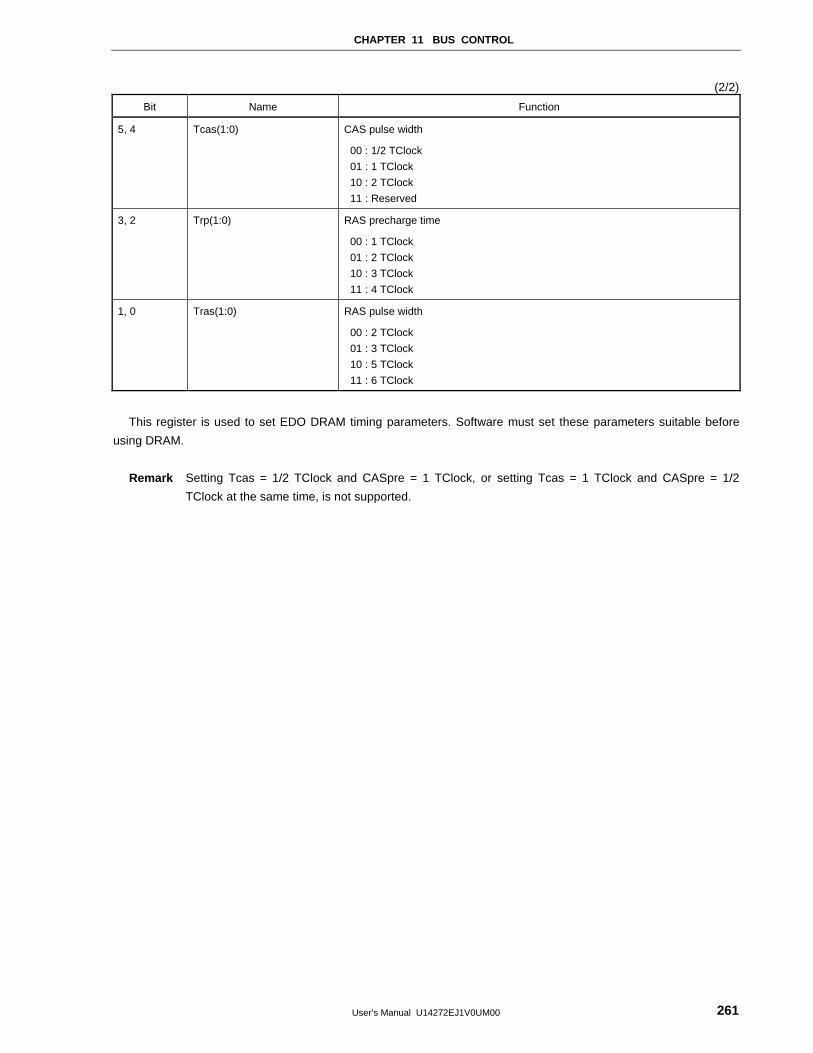
CHAPTER 11 BUS CONTROL
User’s Manual U14272EJ1V0UM00 261
(2/2)
Bit Name Function
5, 4 Tcas(1:0) CAS pulse width
00 : 1/2 TClock
01 : 1 TClock
10 : 2 TClock
11 : Reserved
3, 2 Trp(1:0) RAS precharge time
00 : 1 TClock
01 : 2 TClock
10 : 3 TClock
11 : 4 TClock
1, 0 Tras(1:0) RAS pulse width
00 : 2 TClock
01 : 3 TClock
10 : 5 TClock
11 : 6 TClock
This register is used to set EDO DRAM timing parameters. Software must set these parameters suitable before
using DRAM.
Remark Setting Tcas = 1/2 TClock and CASpre = 1 TClock, or setting Tcas = 1 TClock and CASpre = 1/2
TClock at the same time, is not supported.
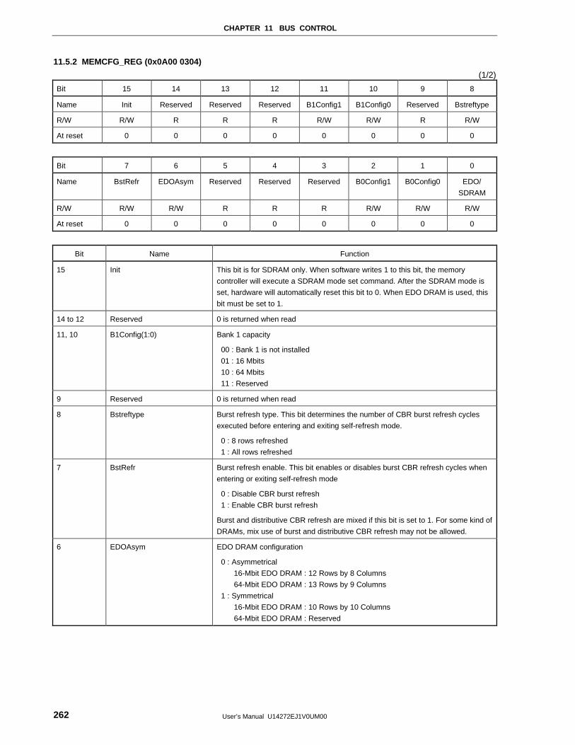
CHAPTER 11 BUS CONTROL
User’s Manual U14272EJ1V0UM00262
11.5.2 MEMCFG_REG (0x0A00 0304)
(1/2)
Bit 15 14 13 12 11 10 9 8
Name Init Reserved Reserved Reserved B1Config1 B1Config0 Reserved Bstreftype
R/W R/W R R R R/W R/W R R/W
At reset 0 0 0 0 0 0 0 0
Bit 7 6 5 4 3 2 1 0
Name BstRefr EDOAsym Reserved Reserved Reserved B0Config1 B0Config0 EDO/
SDRAM
R/W R/W R/W R R R R/W R/W R/W
At reset 0 0 0 0 0 0 0 0
Bit Name Function
15 Init This bit is for SDRAM only. When software writes 1 to this bit, the memory
controller will execute a SDRAM mode set command. After the SDRAM mode is
set, hardware will automatically reset this bit to 0. When EDO DRAM is used, this
bit must be set to 1.
14 to 12 Reserved 0 is returned when read
11, 10 B1Config(1:0) Bank 1 capacity
00 : Bank 1 is not installed
01 : 16 Mbits
10 : 64 Mbits
11 : Reserved
9 Reserved 0 is returned when read
8 Bstreftype Burst refresh type. This bit determines the number of CBR burst refresh cycles
executed before entering and exiting self-refresh mode.
0 : 8 rows refreshed
1 : All rows refreshed
7 BstRefr Burst refresh enable. This bit enables or disables burst CBR refresh cycles when
entering or exiting self-refresh mode
0 : Disable CBR burst refresh
1 : Enable CBR burst refresh
Burst and distributive CBR refresh are mixed if this bit is set to 1. For some kind of
DRAMs, mix use of burst and distributive CBR refresh may not be allowed.
6 EDOAsym EDO DRAM configuration
0 : Asymmetrical
16-Mbit EDO DRAM : 12 Rows by 8 Columns
64-Mbit EDO DRAM : 13 Rows by 9 Columns
1 : Symmetrical
16-Mbit EDO DRAM : 10 Rows by 10 Columns
64-Mbit EDO DRAM : Reserved
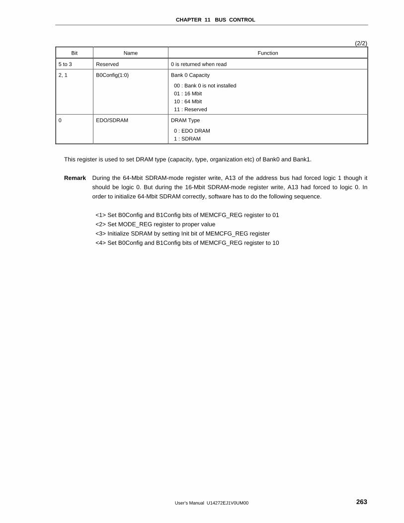
CHAPTER 11 BUS CONTROL
User’s Manual U14272EJ1V0UM00 263
(2/2)
Bit Name Function
5 to 3 Reserved 0 is returned when read
2, 1 B0Config(1:0) Bank 0 Capacity
00 : Bank 0 is not installed
01 : 16 Mbit
10 : 64 Mbit
11 : Reserved
0 EDO/SDRAM DRAM Type
0 : EDO DRAM
1 : SDRAM
This register is used to set DRAM type (capacity, type, organization etc) of Bank0 and Bank1.
Remark During the 64-Mbit SDRAM-mode register write, A13 of the address bus had forced logic 1 though it
should be logic 0. But during the 16-Mbit SDRAM-mode register write, A13 had forced to logic 0. In
order to initialize 64-Mbit SDRAM correctly, software has to do the following sequence.
<1> Set B0Config and B1Config bits of MEMCFG_REG register to 01
<2> Set MODE_REG register to proper value
<3> Initialize SDRAM by setting Init bit of MEMCFG_REG register
<4> Set B0Config and B1Config bits of MEMCFG_REG register to 10
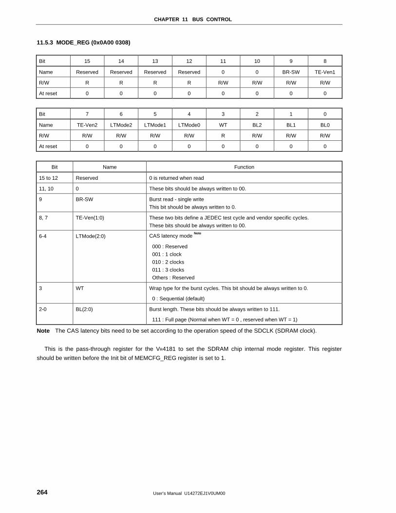
CHAPTER 11 BUS CONTROL
User’s Manual U14272EJ1V0UM00264
11.5.3 MODE_REG (0x0A00 0308)
Bit 15 14 13 12 11 10 9 8
Name Reserved Reserved Reserved Reserved 0 0 BR-SW TE-Ven1
R/W R R R R R/W R/W R/W R/W
At reset 0 0 0 0 0 0 0 0
Bit 7 6 5 4 3 2 1 0
Name TE-Ven2 LTMode2 LTMode1 LTMode0 WT BL2 BL1 BL0
R/W R/W R/W R/W R/W R R/W R/W R/W
At reset 0 0 0 0 0 0 0 0
Bit Name Function
15 to 12 Reserved 0 is returned when read
11, 10 0 These bits should be always written to 00.
9 BR-SW Burst read - single write
This bit should be always written to 0.
8, 7 TE-Ven(1:0) These two bits define a JEDEC test cycle and vendor specific cycles.
These bits should be always written to 00.
6-4 LTMode(2:0) CAS latency mode Note
000 : Reserved
001 : 1 clock
010 : 2 clocks
011 : 3 clocks
Others : Reserved
3 WT Wrap type for the burst cycles. This bit should be always written to 0.
0 : Sequential (default)
2-0 BL(2:0) Burst length. These bits should be always written to 111.
111 : Full page (Normal when WT = 0 , reserved when WT = 1)
Note The CAS latency bits need to be set according to the operation speed of the SDCLK (SDRAM clock).
This is the pass-through register for the VR4181 to set the SDRAM chip internal mode register. This register
should be written before the Init bit of MEMCFG_REG register is set to 1.
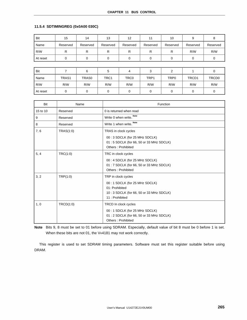
CHAPTER 11 BUS CONTROL
User’s Manual U14272EJ1V0UM00 265
11.5.4 SDTIMINGREG (0x0A00 030C)
Bit 15 14 13 12 11 10 9 8
Name Reserved Reserved Reserved Reserved Reserved Reserved Reserved Reserved
R/W R R R R R R R/W R/W
At reset 0 0 0 0 0 0 0 0
Bit 7 6 5 4 3 2 1 0
Name TRAS1 TRAS0 TRC1 TRC0 TRP1 TRP0 TRCD1 TRCD0
R/W R/W R/W R/W R/W R/W R/W R/W R/W
At reset 0 0 0 0 0 0 0 0
Bit Name Function
15 to 10 Reserved 0 is returned when read
9 Reserved Write 0 when write. Note
8 Reserved Write 1 when write. Note
7, 6 TRAS(1:0) TRAS in clock cycles
00 : 3 SDCLK (for 25 MHz SDCLK)
01 : 5 SDCLK (for 66, 50 or 33 MHz SDCLK)
Others : Prohibited
5, 4 TRC(1:0) TRC in clock cycles
00 : 4 SDCLK (for 25 MHz SDCLK)
01 : 7 SDCLK (for 66, 50 or 33 MHz SDCLK)
Others : Prohibited
3, 2 TRP(1:0) TRP in clock cycles
00 : 1 SDCLK (for 25 MHz SDCLK)
01: Prohibited
10 : 3 SDCLK (for 66, 50 or 33 MHz SDCLK)
11 : Prohibited
1, 0 TRCD(1:0) TRCD In clock cycles
00 : 1 SDCLK (for 25 MHz SDCLK)
01 : 2 SDCLK (for 66, 50 or 33 MHz SDCLK)
Others : Prohibited
Note Bits 9, 8 must be set to 01 before using SDRAM. Especially, default value of bit 8 must be 0 before 1 is set.
When these bits are not 01, the VR4181 may not work correctly.
This register is used to set SDRAM timing parameters. Software must set this register suitable before using
DRAM.
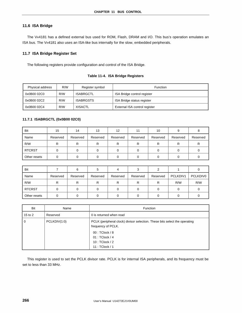
CHAPTER 11 BUS CONTROL
User’s Manual U14272EJ1V0UM00266
11.6 ISA Bridge
The VR4181 has a defined external bus used for ROM, Flash, DRAM and I/O. This bus’s operation emulates an
ISA bus. The VR4181 also uses an ISA-like bus internally for the slow, embedded peripherals.
11.7 ISA Bridge Register Set
The following registers provide configuration and control of the ISA Bridge.
Table 11-4. ISA Bridge Registers
Physical address R/W Register symbol Function
0x0B00 02C0 R/W ISABRGCTL ISA Bridge control register
0x0B00 02C2 R/W ISABRGSTS ISA Bridge status register
0x0B00 02C4 R/W XISACTL External ISA control register
11.7.1 ISABRGCTL (0x0B00 02C0)
Bit 15 14 13 12 11 10 9 8
Name Reserved Reserved Reserved Reserved Reserved Reserved Reserved Reserved
R/W R R R R R R R R
RTCRST 0 0 0 0 0 0 0 0
Other resets 0 0 0 0 0 0 0 0
Bit 7 6 5 4 3 2 1 0
Name Reserved Reserved Reserved Reserved Reserved Reserved PCLKDIV1 PCLKDIV0
R/W R R R R R R R/W R/W
RTCRST 0 0 0 0 0 0 0 0
Other resets 0 0 0 0 0 0 0 0
Bit Name Function
15 to 2 Reserved 0 is returned when read
0 PCLKDIV(1:0) PCLK (peripheral clock) divisor selection. These bits select the operating
frequency of PCLK.
00 : TClock / 8
01 : TClock / 4
10 : TClock / 2
11 : TClock / 1
This register is used to set the PCLK divisor rate. PCLK is for internal ISA peripherals, and its frequency must be
set to less than 33 MHz.
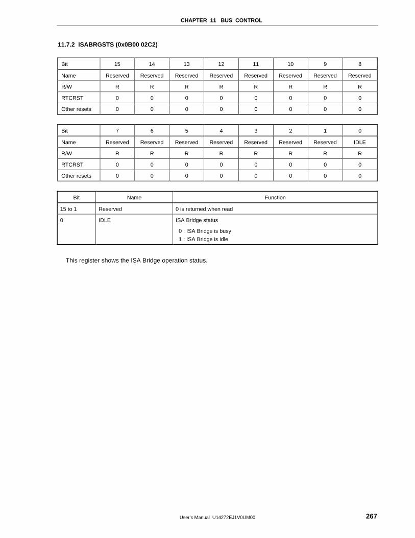
CHAPTER 11 BUS CONTROL
User’s Manual U14272EJ1V0UM00 267
11.7.2 ISABRGSTS (0x0B00 02C2)
Bit 15 14 13 12 11 10 9 8
Name Reserved Reserved Reserved Reserved Reserved Reserved Reserved Reserved
R/W R R R R R R R R
RTCRST 0 0 0 0 0 0 0 0
Other resets 0 0 0 0 0 0 0 0
Bit 7 6 5 4 3 2 1 0
Name Reserved Reserved Reserved Reserved Reserved Reserved Reserved IDLE
R/W R R R R R R R R
RTCRST 0 0 0 0 0 0 0 0
Other resets 0 0 0 0 0 0 0 0
Bit Name Function
15 to 1 Reserved 0 is returned when read
0 IDLE ISA Bridge status
0 : ISA Bridge is busy
1 : ISA Bridge is idle
This register shows the ISA Bridge operation status.
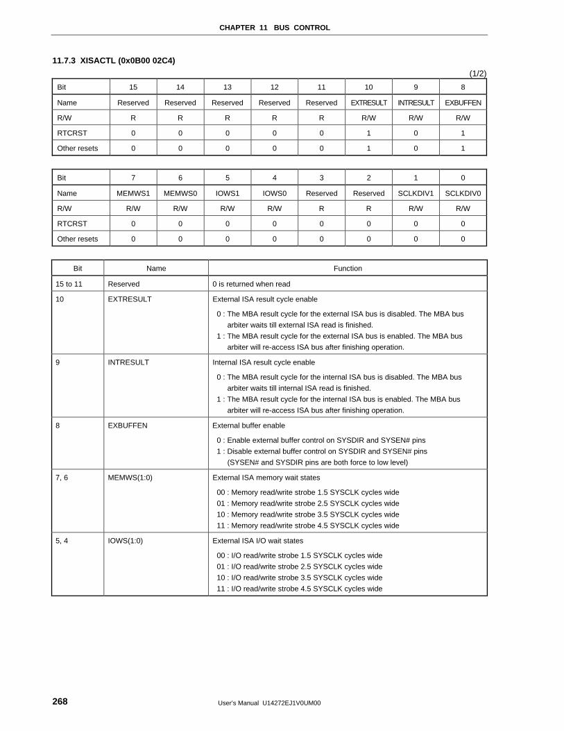
CHAPTER 11 BUS CONTROL
User’s Manual U14272EJ1V0UM00268
11.7.3 XISACTL (0x0B00 02C4)
(1/2)
Bit 15 14 13 12 11 10 9 8
Name Reserved Reserved Reserved Reserved Reserved EXTRESULT INTRESULT EXBUFFEN
R/W R R R R R R/W R/W R/W
RTCRST 0 0 0 0 0 1 0 1
Other resets 0 0 0 0 0 1 0 1
Bit 7 6 5 4 3 2 1 0
Name MEMWS1 MEMWS0 IOWS1 IOWS0 Reserved Reserved SCLKDIV1 SCLKDIV0
R/W R/W R/W R/W R/W R R R/W R/W
RTCRST 0 0 0 0 0 0 0 0
Other resets 0 0 0 0 0 0 0 0
Bit Name Function
15 to 11 Reserved 0 is returned when read
10 EXTRESULT External ISA result cycle enable
0 : The MBA result cycle for the external ISA bus is disabled. The MBA bus
arbiter waits till external ISA read is finished.
1 : The MBA result cycle for the external ISA bus is enabled. The MBA bus
arbiter will re-access ISA bus after finishing operation.
9 INTRESULT Internal ISA result cycle enable
0 : The MBA result cycle for the internal ISA bus is disabled. The MBA bus
arbiter waits till internal ISA read is finished.
1 : The MBA result cycle for the internal ISA bus is enabled. The MBA bus
arbiter will re-access ISA bus after finishing operation.
8 EXBUFFEN External buffer enable
0 : Enable external buffer control on SYSDIR and SYSEN# pins
1 : Disable external buffer control on SYSDIR and SYSEN# pins
(SYSEN# and SYSDIR pins are both force to low level)
7, 6 MEMWS(1:0) External ISA memory wait states
00 : Memory read/write strobe 1.5 SYSCLK cycles wide
01 : Memory read/write strobe 2.5 SYSCLK cycles wide
10 : Memory read/write strobe 3.5 SYSCLK cycles wide
11 : Memory read/write strobe 4.5 SYSCLK cycles wide
5, 4 IOWS(1:0) External ISA I/O wait states
00 : I/O read/write strobe 1.5 SYSCLK cycles wide
01 : I/O read/write strobe 2.5 SYSCLK cycles wide
10 : I/O read/write strobe 3.5 SYSCLK cycles wide
11 : I/O read/write strobe 4.5 SYSCLK cycles wide
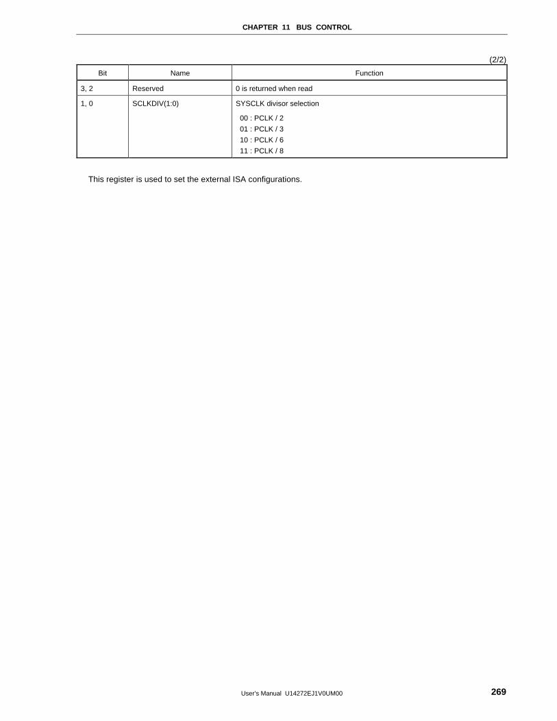
CHAPTER 11 BUS CONTROL
User’s Manual U14272EJ1V0UM00 269
(2/2)
Bit Name Function
3, 2 Reserved 0 is returned when read
1, 0 SCLKDIV(1:0) SYSCLK divisor selection
00 : PCLK / 2
01 : PCLK / 3
10 : PCLK / 6
11 : PCLK / 8
This register is used to set the external ISA configurations.

User’s Manual U14272EJ1V0UM00270
[MEMO]
User’s Manual U14272EJ1V0UM00 271
CHAPTER 12 DMA CONTROL UNIT (DCU)
12.1 General
The DMA Control Unit (DCU) controls four channels of DMA transfer. Two of them are allocated for the AIU
(microphone and speaker), though the remaining two are reserved for future use.
The Microphone channel performs the I/O-to-memory transfers from the ADC included in the AIU to memory. The
Speaker channel performs the memory-to-I/O transfers from memory to the DAC included in the AIU.
Each DMA channel supports both a primary and a secondary memory buffer. The Source1/Source2 or
Destination1/Destination2 Address registers for the associated channel determine the starting address of each
memory buffer. The sizes of memory buffers are determined in the associated Record Length registers.
The DCU uses the primary and secondary DMA buffers alternately when transferring. For example, during the first
DMA transfer following either hardware or software reset of the DCU, DMA transfers will start using the primary DMA
buffer. If the total number of DMA transfers through the primary DMA buffer reaches the value set in the associated
record length register, the next DMA transfer will be performed using the secondary DMA buffer. Software must keep
track of which buffer contains valid DMA data.
Software may configure any of the DMA channels to operate in one of two modes; auto stop or auto load. When a
channel is configured to operate in auto stop mode, the DCU terminates DMA transfers after the number of transfers
specified by the record length register and automatically resets the DMA mask bit for that channel. Once the mask bit
is automatically reset, the DCU ignores all subsequent DMA requests for this channel. To resume DMA transfers in
this mode, software must again unmask DMA transfers for this channel. Once software unmasks DMA requests, the
DCU will resume DMA transfers utilizing the secondary memory buffer.
When configured for auto load mode, the DCU does not terminate DMA transfers after the number of DMA
transfers specified by the record length register. Instead, the DCU will automatically switch to the secondary DMA
buffer and continue servicing DMA requests.
In either mode, auto stop or auto load, the DCU always alternates memory transfers between the primary and
secondary DMA buffers. Software must keep track of the total number of transfers and assure the appropriate DMA
buffer is loaded with new DMA data before starting another DMA transfer.
The DCU may be programmed to generate an EOP interrupt request independent of auto stop or auto load mode.
The EOP interrupt request is generated once the number of DMA transfers specified by the record length register has
occurred.
CHAPTER 12 DMA CONTROL UNIT (DCU)
User’s Manual U14272EJ1V0UM00272
Priority of each DMA channel is fixed. The channel priority is as follows.
1. AIU Microphone channel
2. AIU Speaker channel
DCU runs at the MBA bus clock (TClock) frequency.
Remark The DCU contains a 32-bit temporary storage register for each DMA channel. For memory-to-I/O
transfers, the DCU performs a 32-bit memory read from DRAM and stores the read data into the
temporary storage register. The DCU then transfers data from this register to the target I/O device. For
a 16-bit device such as the Speaker channel, the DCU will perform 2 I/O writes to the DAC for each
memory read.
During DMA transfers, all DCU registers are write-protected if valid data is present in the temporary
storage registers. Because of this, when DMA transfers are running, software must read a DMA register
after write to confirm that the register has been correctly set.
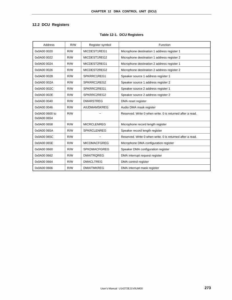
CHAPTER 12 DMA CONTROL UNIT (DCU)
User’s Manual U14272EJ1V0UM00 273
12.2 DCU Registers
Table 12-1. DCU Registers
Address R/W Register symbol Function
0x0A00 0020 R/W MICDEST1REG1 Microphone destination 1 address register 1
0x0A00 0022 R/W MICDEST1REG2 Microphone destination 1 address register 2
0x0A00 0024 R/W MICDEST2REG1 Microphone destination 2 address register 1
0x0A00 0026 R/W MICDEST2REG2 Microphone destination 2 address register 2
0x0A00 0028 R/W SPKRRC1REG1 Speaker source 1 address register 1
0x0A00 002A R/W SPKRRC1REG2 Speaker source 1 address register 2
0x0A00 002C R/W SPKRRC2REG1 Speaker source 2 address register 1
0x0A00 002E R/W SPKRRC2REG2 Speaker source 2 address register 2
0x0A00 0040 R/W DMARSTREG DMA reset register
0x0A00 0046 R/W AIUDMAMSKREG Audio DMA mask register
0x0A00 0600 to
0x0A00 0654
R/W − Reserved. Write 0 when write. 0 is returned after a read.
0x0A00 0658 R/W MICRCLENREG Microphone record length register
0x0A00 065A R/W SPKRCLENREG Speaker record length register
0x0A00 065C R/W − Reserved. Write 0 when write. 0 is returned after a read.
0x0A00 065E R/W MICDMACFGREG Microphone DMA configuration register
0x0A00 0660 R/W SPKDMACFGREG Speaker DMA configuration register
0x0A00 0662 R/W DMAITRQREG DMA interrupt request register
0x0A00 0664 R/W DMACLTREG DMA control register
0x0A00 0666 R/W DMAITMKREG DMA interrupt mask register
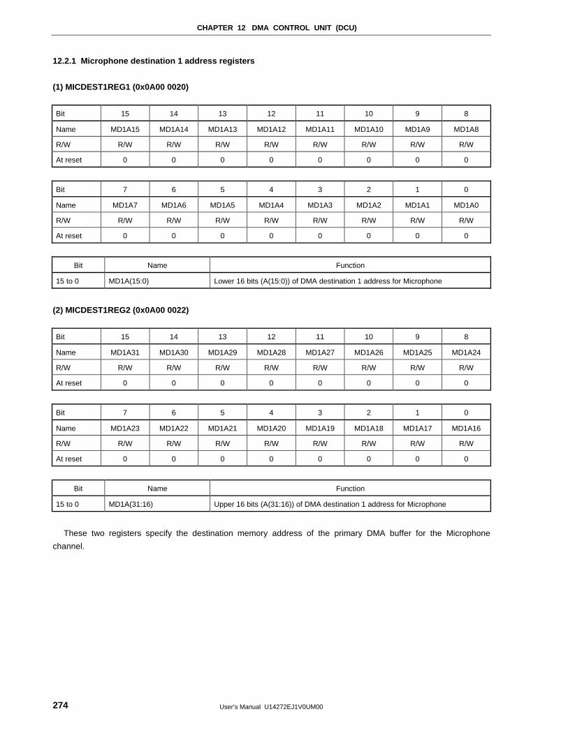
CHAPTER 12 DMA CONTROL UNIT (DCU)
User’s Manual U14272EJ1V0UM00274
12.2.1 Microphone destination 1 address registers
(1) MICDEST1REG1 (0x0A00 0020)
Bit 15 14 13 12 11 10 9 8
Name MD1A15 MD1A14 MD1A13 MD1A12 MD1A11 MD1A10 MD1A9 MD1A8
R/W R/W R/W R/W R/W R/W R/W R/W R/W
At reset 0 0 0 0 0 0 0 0
Bit 7 6 5 4 3 2 1 0
Name MD1A7 MD1A6 MD1A5 MD1A4 MD1A3 MD1A2 MD1A1 MD1A0
R/W R/W R/W R/W R/W R/W R/W R/W R/W
At reset 0 0 0 0 0 0 0 0
Bit Name Function
15 to 0 MD1A(15:0) Lower 16 bits (A(15:0)) of DMA destination 1 address for Microphone
(2) MICDEST1REG2 (0x0A00 0022)
Bit 15 14 13 12 11 10 9 8
Name MD1A31 MD1A30 MD1A29 MD1A28 MD1A27 MD1A26 MD1A25 MD1A24
R/W R/W R/W R/W R/W R/W R/W R/W R/W
At reset 0 0 0 0 0 0 0 0
Bit 7 6 5 4 3 2 1 0
Name MD1A23 MD1A22 MD1A21 MD1A20 MD1A19 MD1A18 MD1A17 MD1A16
R/W R/W R/W R/W R/W R/W R/W R/W R/W
At reset 0 0 0 0 0 0 0 0
Bit Name Function
15 to 0 MD1A(31:16) Upper 16 bits (A(31:16)) of DMA destination 1 address for Microphone
These two registers specify the destination memory address of the primary DMA buffer for the Microphone
channel.
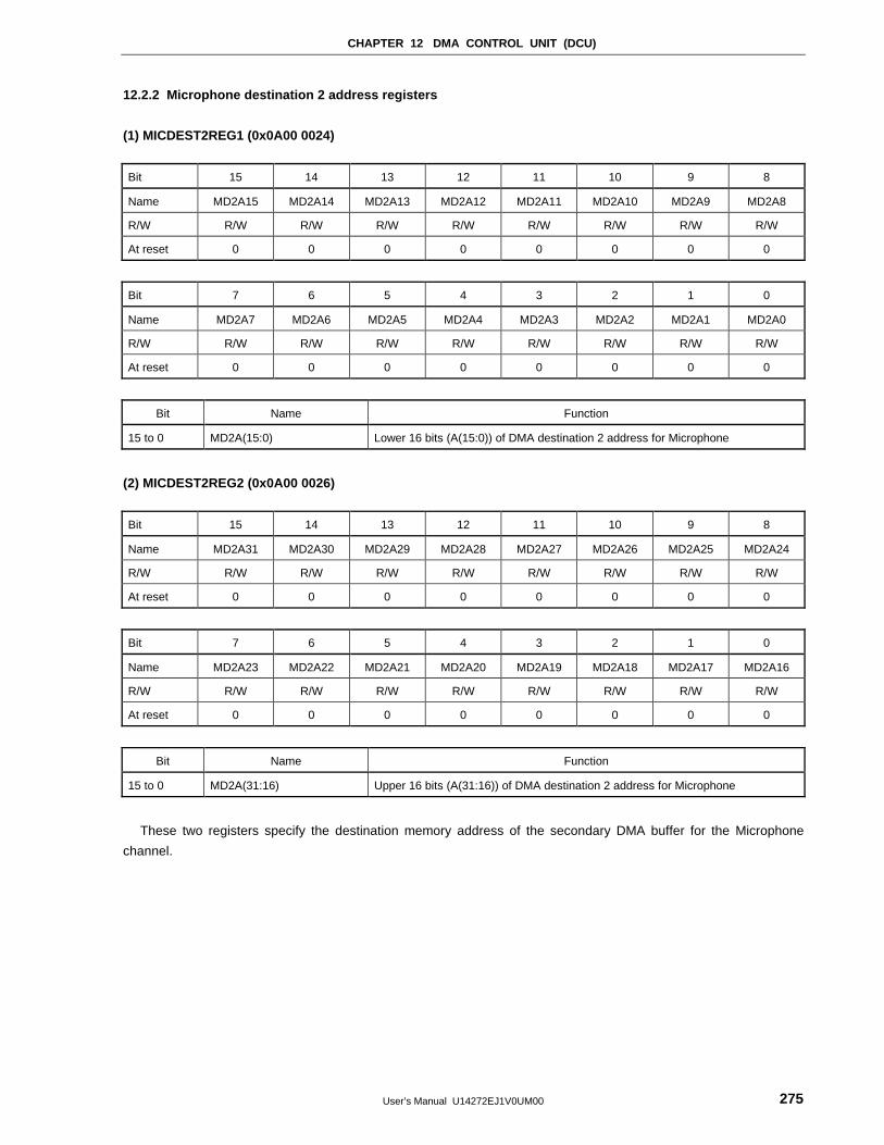
CHAPTER 12 DMA CONTROL UNIT (DCU)
User’s Manual U14272EJ1V0UM00 275
12.2.2 Microphone destination 2 address registers
(1) MICDEST2REG1 (0x0A00 0024)
Bit 15 14 13 12 11 10 9 8
Name MD2A15 MD2A14 MD2A13 MD2A12 MD2A11 MD2A10 MD2A9 MD2A8
R/W R/W R/W R/W R/W R/W R/W R/W R/W
At reset 0 0 0 0 0 0 0 0
Bit 7 6 5 4 3 2 1 0
Name MD2A7 MD2A6 MD2A5 MD2A4 MD2A3 MD2A2 MD2A1 MD2A0
R/W R/W R/W R/W R/W R/W R/W R/W R/W
At reset 0 0 0 0 0 0 0 0
Bit Name Function
15 to 0 MD2A(15:0) Lower 16 bits (A(15:0)) of DMA destination 2 address for Microphone
(2) MICDEST2REG2 (0x0A00 0026)
Bit 15 14 13 12 11 10 9 8
Name MD2A31 MD2A30 MD2A29 MD2A28 MD2A27 MD2A26 MD2A25 MD2A24
R/W R/W R/W R/W R/W R/W R/W R/W R/W
At reset 0 0 0 0 0 0 0 0
Bit 7 6 5 4 3 2 1 0
Name MD2A23 MD2A22 MD2A21 MD2A20 MD2A19 MD2A18 MD2A17 MD2A16
R/W R/W R/W R/W R/W R/W R/W R/W R/W
At reset 0 0 0 0 0 0 0 0
Bit Name Function
15 to 0 MD2A(31:16) Upper 16 bits (A(31:16)) of DMA destination 2 address for Microphone
These two registers specify the destination memory address of the secondary DMA buffer for the Microphone
channel.
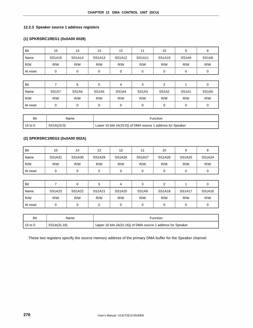
CHAPTER 12 DMA CONTROL UNIT (DCU)
User’s Manual U14272EJ1V0UM00276
12.2.3 Speaker source 1 address registers
(1) SPKRSRC1REG1 (0x0A00 0028)
Bit 15 14 13 12 11 10 9 8
Name SS1A15 SS1A14 SS1A13 SS1A12 SS1A11 SS1A10 SS1A9 SS1A8
R/W R/W R/W R/W R/W R/W R/W R/W R/W
At reset 0 0 0 0 0 0 0 0
Bit 7 6 5 4 3 2 1 0
Name SS1A7 SS1A6 SS1A5 SS1A4 SS1A3 SS1A2 SS1A1 SS1A0
R/W R/W R/W R/W R/W R/W R/W R/W R/W
At reset 0 0 0 0 0 0 0 0
Bit Name Function
15 to 0 SS1A(15:0) Lower 16 bits (A(15:0)) of DMA source 1 address for Speaker
(2) SPKRSRC1REG2 (0x0A00 002A)
Bit 15 14 13 12 11 10 9 8
Name SS1A31 SS1A30 SS1A29 SS1A28 SS1A27 SS1A26 SS1A25 SS1A24
R/W R/W R/W R/W R/W R/W R/W R/W R/W
At reset 0 0 0 0 0 0 0 0
Bit 7 6 5 4 3 2 1 0
Name SS1A23 SS1A22 SS1A21 SS1A20 SS1A9 SS1A18 SS1A17 SS1A16
R/W R/W R/W R/W R/W R/W R/W R/W R/W
At reset 0 0 0 0 0 0 0 0
Bit Name Function
15 to 0 SS1A(31:16) Upper 16 bits (A(31:16)) of DMA source 1 address for Speaker
These two registers specify the source memory address of the primary DMA buffer for the Speaker channel.
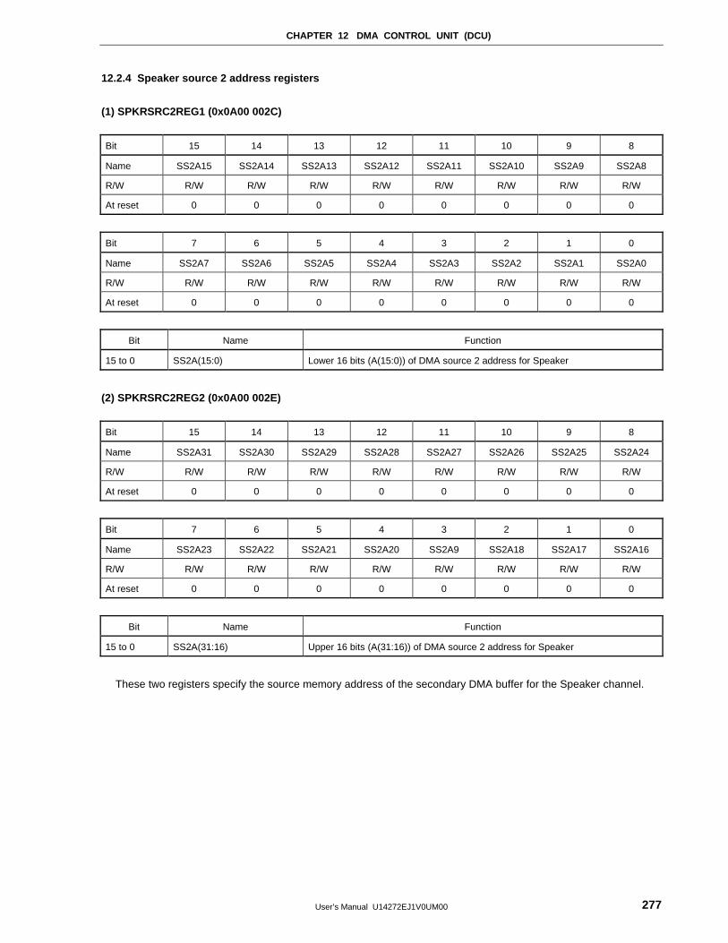
CHAPTER 12 DMA CONTROL UNIT (DCU)
User’s Manual U14272EJ1V0UM00 277
12.2.4 Speaker source 2 address registers
(1) SPKRSRC2REG1 (0x0A00 002C)
Bit 15 14 13 12 11 10 9 8
Name SS2A15 SS2A14 SS2A13 SS2A12 SS2A11 SS2A10 SS2A9 SS2A8
R/W R/W R/W R/W R/W R/W R/W R/W R/W
At reset 0 0 0 0 0 0 0 0
Bit 7 6 5 4 3 2 1 0
Name SS2A7 SS2A6 SS2A5 SS2A4 SS2A3 SS2A2 SS2A1 SS2A0
R/W R/W R/W R/W R/W R/W R/W R/W R/W
At reset 0 0 0 0 0 0 0 0
Bit Name Function
15 to 0 SS2A(15:0) Lower 16 bits (A(15:0)) of DMA source 2 address for Speaker
(2) SPKRSRC2REG2 (0x0A00 002E)
Bit 15 14 13 12 11 10 9 8
Name SS2A31 SS2A30 SS2A29 SS2A28 SS2A27 SS2A26 SS2A25 SS2A24
R/W R/W R/W R/W R/W R/W R/W R/W R/W
At reset 0 0 0 0 0 0 0 0
Bit 7 6 5 4 3 2 1 0
Name SS2A23 SS2A22 SS2A21 SS2A20 SS2A9 SS2A18 SS2A17 SS2A16
R/W R/W R/W R/W R/W R/W R/W R/W R/W
At reset 0 0 0 0 0 0 0 0
Bit Name Function
15 to 0 SS2A(31:16) Upper 16 bits (A(31:16)) of DMA source 2 address for Speaker
These two registers specify the source memory address of the secondary DMA buffer for the Speaker channel.
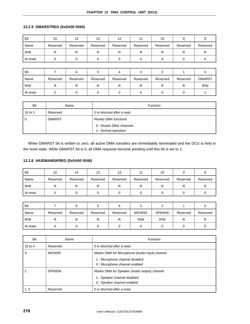
CHAPTER 12 DMA CONTROL UNIT (DCU)
User’s Manual U14272EJ1V0UM00278
12.2.5 DMARSTREG (0x0A00 0040)
Bit 15 14 13 12 11 10 9 8
Name Reserved Reserved Reserved Reserved Reserved Reserved Reserved Reserved
R/W R R R R R R R R
At reset 0 0 0 0 0 0 0 0
Bit 7 6 5 4 3 2 1 0
Name Reserved Reserved Reserved Reserved Reserved Reserved Reserved DMARST
R/W R R R R R R R R/W
At reset 0 0 0 0 0 0 0 1
Bit Name Function
15 to 1 Reserved 0 is returned after a read.
0 DMARST Resets DMA functions
0 : Resets DMA channels
1 : Normal operation
When DMARST bit is written to zero, all active DMA transfers are immediately terminated and the DCU is held in
the reset state. While DMARST bit is 0, all DMA requests become pending until this bit is set to 1.
12.2.6 AIUDMAMSKREG (0x0A00 0046)
Bit 15 14 13 12 11 10 9 8
Name Reserved Reserved Reserved Reserved Reserved Reserved Reserved Reserved
R/W R R R R R R R R
At reset 0 0 0 0 0 0 0 0
Bit 7 6 5 4 3 2 1 0
Name Reserved Reserved Reserved Reserved MICMSK SPKMSK Reserved Reserved
R/W R R R R R/W R/W R R
At reset 0 0 0 0 0 0 0 0
Bit Name Function
15 to 4 Reserved 0 is returned after a read.
3 MICMSK Masks DMA for Microphone (Audio input) channel
1 : Microphone channel disabled
0 : Microphone channel enabled
2 SPKMSK Masks DMA for Speaker (Audio output) channel
1 : Speaker channel disabled
0 : Speaker channel enabled
1, 0 Reserved 0 is returned after a read.
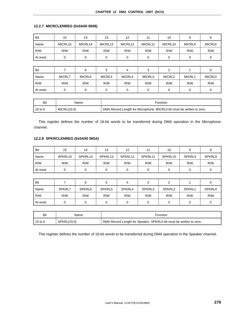
CHAPTER 12 DMA CONTROL UNIT (DCU)
User’s Manual U14272EJ1V0UM00 279
12.2.7 MICRCLENREG (0x0A00 0658)
Bit 15 14 13 12 11 10 9 8
Name MICRL15 MICRL14 MICRL13 MICRL12 MICRL11 MICRL10 MICRL9 MICRL8
R/W R/W R/W R/W R/W R/W R/W R/W R/W
At reset 0 0 0 0 0 0 0 0
Bit 7 6 5 4 3 2 1 0
Name MICRL7 MICRL6 MICRL5 MICRL4 MICRL3 MICRL2 MICRL1 MICRL0
R/W R/W R/W R/W R/W R/W R/W R/W R/W
At reset 0 0 0 0 0 0 0 0
Bit Name Function
15 to 0 MICRL(15:0) DMA Record Length for Microphone. MICRL0 bit must be written to zero.
This register defines the number of 16-bit words to be transferred during DMA operation in the Microphone
channel.
12.2.8 SPKRCLENREG (0x0A00 065A)
Bit 15 14 13 12 11 10 9 8
Name SPKRL15 SPKRL14 SPKRL13 SPKRL12 SPKRL11 SPKRL10 SPKRL9 SPKRL8
R/W R/W R/W R/W R/W R/W R/W R/W R/W
At reset 0 0 0 0 0 0 0 0
Bit 7 6 5 4 3 2 1 0
Name SPKRL7 SPKRL6 SPKRL5 SPKRL4 SPKRL3 SPKRL2 SPKRL1 SPKRL0
R/W R/W R/W R/W R/W R/W R/W R/W R/W
At reset 0 0 0 0 0 0 0 0
Bit Name Function
15 to 0 SPKRL(15:0) DMA Record Length for Speaker. SPKRL0 bit must be written to zero.
This register defines the number of 16-bit words to be transferred during DMA operation in the Speaker channel.
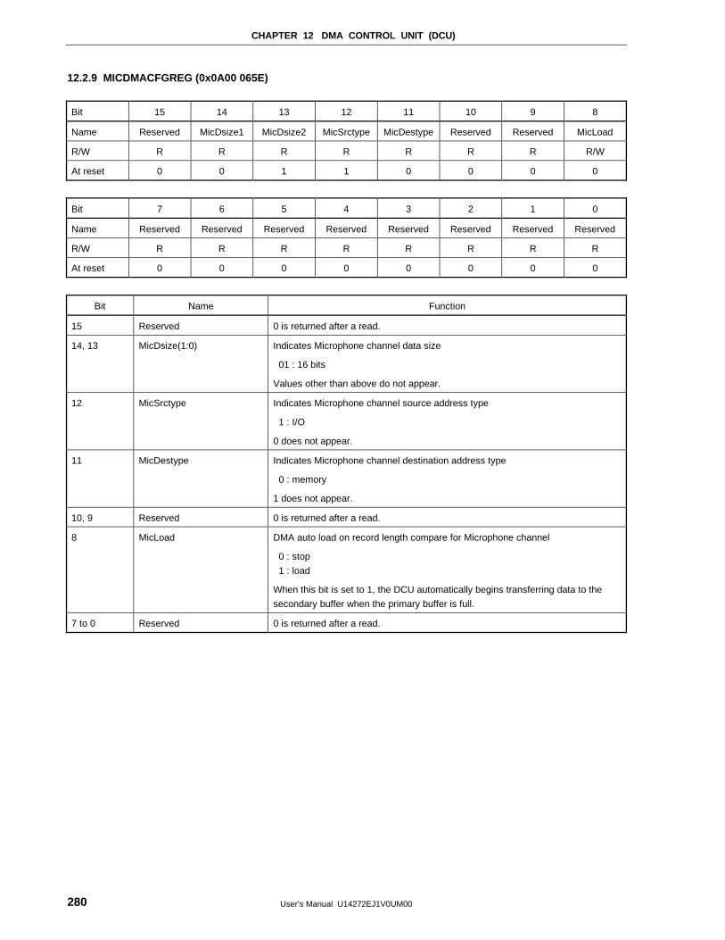
CHAPTER 12 DMA CONTROL UNIT (DCU)
User’s Manual U14272EJ1V0UM00280
12.2.9 MICDMACFGREG (0x0A00 065E)
Bit 15 14 13 12 11 10 9 8
Name Reserved MicDsize1 MicDsize2 MicSrctype MicDestype Reserved Reserved MicLoad
R/W R R R R R R R R/W
At reset 0 0 1 1 0 0 0 0
Bit 7 6 5 4 3 2 1 0
Name Reserved Reserved Reserved Reserved Reserved Reserved Reserved Reserved
R/W R R R R R R R R
At reset 0 0 0 0 0 0 0 0
Bit Name Function
15 Reserved 0 is returned after a read.
14, 13 MicDsize(1:0) Indicates Microphone channel data size
01 : 16 bits
Values other than above do not appear.
12 MicSrctype Indicates Microphone channel source address type
1 : I/O
0 does not appear.
11 MicDestype Indicates Microphone channel destination address type
0 : memory
1 does not appear.
10, 9 Reserved 0 is returned after a read.
8 MicLoad DMA auto load on record length compare for Microphone channel
0 : stop
1 : load
When this bit is set to 1, the DCU automatically begins transferring data to the
secondary buffer when the primary buffer is full.
7 to 0 Reserved 0 is returned after a read.
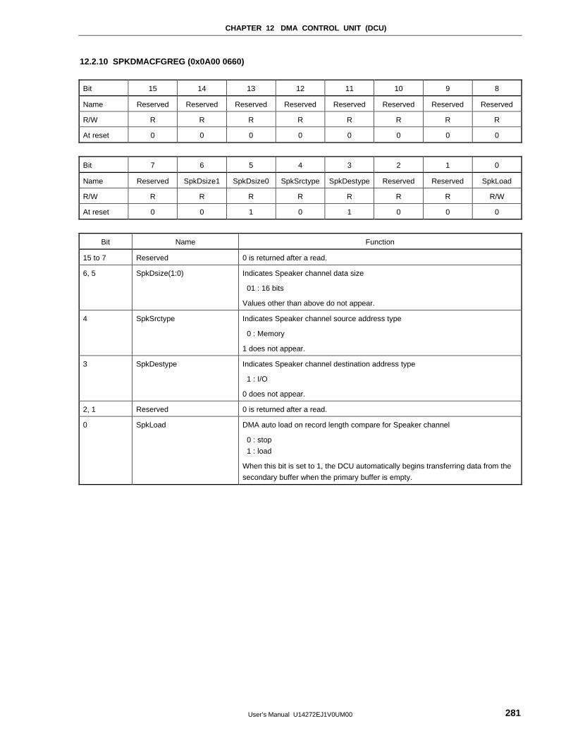
CHAPTER 12 DMA CONTROL UNIT (DCU)
User’s Manual U14272EJ1V0UM00 281
12.2.10 SPKDMACFGREG (0x0A00 0660)
Bit 15 14 13 12 11 10 9 8
Name Reserved Reserved Reserved Reserved Reserved Reserved Reserved Reserved
R/W R R R R R R R R
At reset 0 0 0 0 0 0 0 0
Bit 7 6 5 4 3 2 1 0
Name Reserved SpkDsize1 SpkDsize0 SpkSrctype SpkDestype Reserved Reserved SpkLoad
R/W R R R R R R R R/W
At reset 0 0 1 0 1 0 0 0
Bit Name Function
15 to 7 Reserved 0 is returned after a read.
6, 5 SpkDsize(1:0) Indicates Speaker channel data size
01 : 16 bits
Values other than above do not appear.
4 SpkSrctype Indicates Speaker channel source address type
0 : Memory
1 does not appear.
3 SpkDestype Indicates Speaker channel destination address type
1 : I/O
0 does not appear.
2, 1 Reserved 0 is returned after a read.
0 SpkLoad DMA auto load on record length compare for Speaker channel
0 : stop
1 : load
When this bit is set to 1, the DCU automatically begins transferring data from the
secondary buffer when the primary buffer is empty.
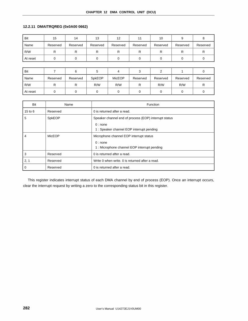
CHAPTER 12 DMA CONTROL UNIT (DCU)
User’s Manual U14272EJ1V0UM00282
12.2.11 DMAITRQREG (0x0A00 0662)
Bit 15 14 13 12 11 10 9 8
Name Reserved Reserved Reserved Reserved Reserved Reserved Reserved Reserved
R/W R R R R R R R R
At reset 0 0 0 0 0 0 0 0
Bit 7 6 5 4 3 2 1 0
Name Reserved Reserved SpkEOP MicEOP Reserved Reserved Reserved Reserved
R/W R R R/W R/W R R/W R/W R
At reset 0 0 0 0 0 0 0 0
Bit Name Function
15 to 6 Reserved 0 is returned after a read.
5 SpkEOP Speaker channel end of process (EOP) interrupt status
0 : none
1 : Speaker channel EOP interrupt pending
4 MicEOP Microphone channel EOP interrupt status
0 : none
1 : Microphone channel EOP interrupt pending
3 Reserved 0 is returned after a read.
2, 1 Reserved Write 0 when write. 0 is returned after a read.
0 Reserved 0 is returned after a read.
This register indicates interrupt status of each DMA channel by end of process (EOP). Once an interrupt occurs,
clear the interrupt request by writing a zero to the corresponding status bit in this register.
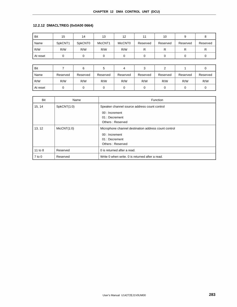
CHAPTER 12 DMA CONTROL UNIT (DCU)
User’s Manual U14272EJ1V0UM00 283
12.2.12 DMACLTREG (0x0A00 0664)
Bit 15 14 13 12 11 10 9 8
Name SpkCNT1 SpkCNT0 MicCNT1 MicCNT0 Reserved Reserved Reserved Reserved
R/W R/W R/W R/W R/W R R R R
At reset 0 0 0 0 0 0 0 0
Bit 7 6 5 4 3 2 1 0
Name Reserved Reserved Reserved Reserved Reserved Reserved Reserved Reserved
R/W R/W R/W R/W R/W R/W R/W R/W R/W
At reset 0 0 0 0 0 0 0 0
Bit Name Function
15, 14 SpkCNT(1:0) Speaker channel source address count control
00 : Increment
01 : Decrement
Others : Reserved
13, 12 MicCNT(1:0) Microphone channel destination address count control
00 : Increment
01 : Decrement
Others : Reserved
11 to 8 Reserved 0 is returned after a read.
7 to 0 Reserved Write 0 when write. 0 is returned after a read.
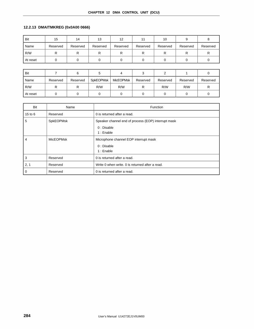
CHAPTER 12 DMA CONTROL UNIT (DCU)
User’s Manual U14272EJ1V0UM00284
12.2.13 DMAITMKREG (0x0A00 0666)
Bit 15 14 13 12 11 10 9 8
Name Reserved Reserved Reserved Reserved Reserved Reserved Reserved Reserved
R/W R R R R R R R R
At reset 0 0 0 0 0 0 0 0
Bit 7 6 5 4 3 2 1 0
Name Reserved Reserved SpkEOPMsk MicEOPMsk Reserved Reserved Reserved Reserved
R/W R R R/W R/W R R/W R/W R
At reset 0 0 0 0 0 0 0 0
Bit Name Function
15 to 6 Reserved 0 is returned after a read.
5 SpkEOPMsk Speaker channel end of process (EOP) interrupt mask
0 : Disable
1 : Enable
4 MicEOPMsk Microphone channel EOP interrupt mask
0 : Disable
1 : Enable
3 Reserved 0 is returned after a read.
2, 1 Reserved Write 0 when write. 0 is returned after a read.
0 Reserved 0 is returned after a read.
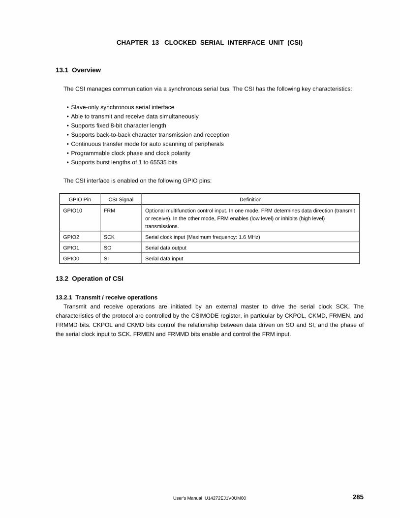
User’s Manual U14272EJ1V0UM00 285
CHAPTER 13 CLOCKED SERIAL INTERFACE UNIT (CSI)
13.1 Overview
The CSI manages communication via a synchronous serial bus. The CSI has the following key characteristics:
• Slave-only synchronous serial interface
• Able to transmit and receive data simultaneously
• Supports fixed 8-bit character length
• Supports back-to-back character transmission and reception
• Continuous transfer mode for auto scanning of peripherals
• Programmable clock phase and clock polarity
• Supports burst lengths of 1 to 65535 bits
The CSI interface is enabled on the following GPIO pins:
GPIO Pin CSI Signal Definition
GPIO10 FRM Optional multifunction control input. In one mode, FRM determines data direction (transmit
or receive). In the other mode, FRM enables (low level) or inhibits (high level)
transmissions.
GPIO2 SCK Serial clock input (Maximum frequency: 1.6 MHz)
GPIO1 SO Serial data output
GPIO0 SI Serial data input
13.2 Operation of CSI
13.2.1 Transmit / receive operations
Transmit and receive operations are initiated by an external master to drive the serial clock SCK. The
characteristics of the protocol are controlled by the CSIMODE register, in particular by CKPOL, CKMD, FRMEN, and
FRMMD bits. CKPOL and CKMD bits control the relationship between data driven on SO and SI, and the phase of
the serial clock input to SCK. FRMEN and FRMMD bits enable and control the FRM input.
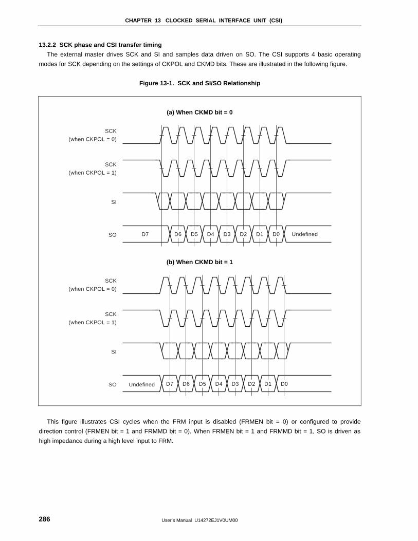
CHAPTER 13 CLOCKED SERIAL INTERFACE UNIT (CSI)
User’s Manual U14272EJ1V0UM00286
13.2.2 SCK phase and CSI transfer timing
The external master drives SCK and SI and samples data driven on SO. The CSI supports 4 basic operating
modes for SCK depending on the settings of CKPOL and CKMD bits. These are illustrated in the following figure.
Figure 13-1. SCK and SI/SO Relationship
(a) When CKMD bit = 0
SCK
(when CKPOL = 0)
SCK
(when CKPOL = 1)
SO
SI
UndefinedD7 D6 D0D5 D4 D3 D2 D1
(b) When CKMD bit = 1
SCK
(when CKPOL = 0)
SCK
(when CKPOL = 1)
SO
SI
Undefined D7 D6 D0D5 D4 D3 D2 D1
This figure illustrates CSI cycles when the FRM input is disabled (FRMEN bit = 0) or configured to provide
direction control (FRMEN bit = 1 and FRMMD bit = 0). When FRMEN bit = 1 and FRMMD bit = 1, SO is driven as
high impedance during a high level input to FRM.
CHAPTER 13 CLOCKED SERIAL INTERFACE UNIT (CSI)
User’s Manual U14272EJ1V0UM00 287
(1) When CKMD = 0 and CKPOL = 0
In this mode, data bit D7 is driven as valid prior to the first rising edge of SCK. Thereafter, data is transmitted at
the falling edge of SCK and sampled by the VR4181 or the external master at the rising edge of SCK.
(2) When CKMD = 0 and CKPOL = 1
In this mode, data bit D7 is driven as valid and then sampled at the first falling edge of SCK. Thereafter, data is
transmitted at the rising edge of SCK and sampled by the VR4181 or the external master at the falling edge of
SCK.
(3) When CKMD = 1 and CKPOL = 0
In this mode, data bit D7 is driven valid on the first rising edge of SCK and sampled at the first falling edge of
SCK. Thereafter, data is transmitted at the rising edge of SCK and sampled by the VR4181 or the external master
at the falling edge of SCK.
(4) When CKMD = 1 and CKPOL = 1
In this mode, data bit D7 is driven as valid at the first falling edge of SCK and sampled at the first rising edge of
SCK. Thereafter, data is transmitted at the falling edge of SCK and sampled by the VR4181 or the external
master at the rising edge of SCK.
13.2.3 CSI Transfer Types
(1) Burst mode
Burst mode is supported for both transmit and receive transfers. Burst lengths for transmit and receive are
independently programmable and can be set from 1 to 65535 bits. The Transmit and Receive shift registers are
both 8-bit lengths. During burst mode, when the receive shift register goes “full”, the data is automatically
transferred to the receive FIFO. When the transmit shift register goes “empty”, it is automatically reloaded from
the transmit FIFO.
Once the burst length has been set and the burst transaction enabled, the CSI behaves as follows:
The CSI begins tracking the number of bits transmitted and/or received. At the end of each bit transfer, the bit
count is updated and compared to the corresponding burst length value (transmit and/or receive). If the number
of bits transferred is equal to the burst length, the CSI shift register is halted.
If the transfer is a reception, the contents of the shift register will be copied to the receive FIFO, a Receive Burst
End interrupt request will be generated if unmasked, and additional activities on the SCK input will be ignored. If
the transfer is a transmission, a Transmit Burst End interrupt request will be generated if unmasked and
additional SCK cycles will cause the data remaining in the transmit shift register to be output on SO.
(2) Continuous mode
Continuous mode transfers are always defined as 8-bit fixed length transfers. In continuous mode, software must
control the flow of data between the VR4181 and the external master.
When continuous mode is enabled and the receive shift register goes “full”, the data is automatically transferred
to the receive FIFO. When the transmit shift register goes “empty”, it is automatically reloaded from the transmit
FIFO.
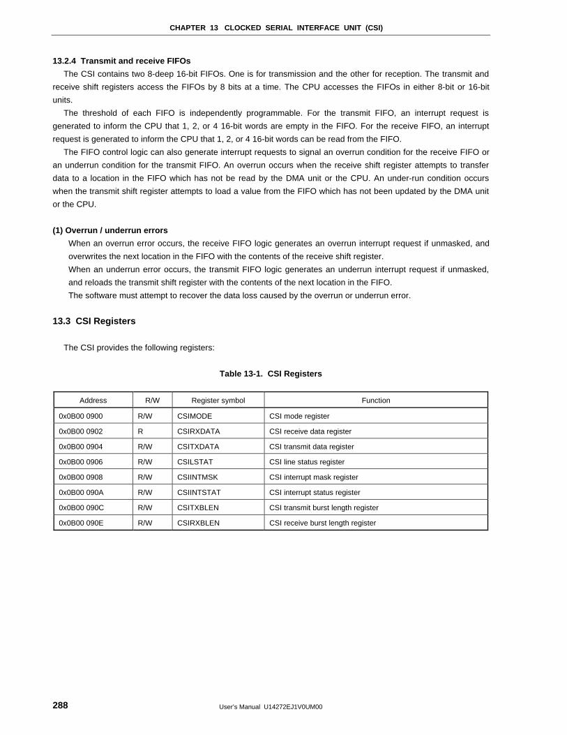
CHAPTER 13 CLOCKED SERIAL INTERFACE UNIT (CSI)
User’s Manual U14272EJ1V0UM00288
13.2.4 Transmit and receive FIFOs
The CSI contains two 8-deep 16-bit FIFOs. One is for transmission and the other for reception. The transmit and
receive shift registers access the FIFOs by 8 bits at a time. The CPU accesses the FIFOs in either 8-bit or 16-bit
units.
The threshold of each FIFO is independently programmable. For the transmit FIFO, an interrupt request is
generated to inform the CPU that 1, 2, or 4 16-bit words are empty in the FIFO. For the receive FIFO, an interrupt
request is generated to inform the CPU that 1, 2, or 4 16-bit words can be read from the FIFO.
The FIFO control logic can also generate interrupt requests to signal an overrun condition for the receive FIFO or
an underrun condition for the transmit FIFO. An overrun occurs when the receive shift register attempts to transfer
data to a location in the FIFO which has not be read by the DMA unit or the CPU. An under-run condition occurs
when the transmit shift register attempts to load a value from the FIFO which has not been updated by the DMA unit
or the CPU.
(1) Overrun / underrun errors
When an overrun error occurs, the receive FIFO logic generates an overrun interrupt request if unmasked, and
overwrites the next location in the FIFO with the contents of the receive shift register.
When an underrun error occurs, the transmit FIFO logic generates an underrun interrupt request if unmasked,
and reloads the transmit shift register with the contents of the next location in the FIFO.
The software must attempt to recover the data loss caused by the overrun or underrun error.
13.3 CSI Registers
The CSI provides the following registers:
Table 13-1. CSI Registers
Address R/W Register symbol Function
0x0B00 0900 R/W CSIMODE CSI mode register
0x0B00 0902 R CSIRXDATA CSI receive data register
0x0B00 0904 R/W CSITXDATA CSI transmit data register
0x0B00 0906 R/W CSILSTAT CSI line status register
0x0B00 0908 R/W CSIINTMSK CSI interrupt mask register
0x0B00 090A R/W CSIINTSTAT CSI interrupt status register
0x0B00 090C R/W CSITXBLEN CSI transmit burst length register
0x0B00 090E R/W CSIRXBLEN CSI receive burst length register
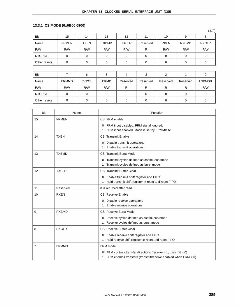
CHAPTER 13 CLOCKED SERIAL INTERFACE UNIT (CSI)
User’s Manual U14272EJ1V0UM00 289
13.3.1 CSIMODE (0x0B00 0900)
(1/2)
Bit 15 14 13 12 11 10 9 8
Name FRMEN TXEN TXBMD TXCLR Reserved RXEN RXBMD RXCLR
R/W R/W R/W R/W R/W R R/W R/W R/W
RTCRST 0 0 0 0 0 0 0 0
Other resets 0 0 0 0 0 0 0 0
Bit 7 6 5 4 3 2 1 0
Name FRMMD CKPOL CKMD Reserved Reserved Reserved Reserved LSBMSB
R/W R/W R/W R/W R R R R R/W
RTCRST 0 0 0 0 0 0 0 0
Other resets 0 0 0 0 0 0 0 0
Bit Name Function
15 FRMEN CSI FRM enable
0 : FRM input disabled. FRM signal ignored.
1 : FRM input enabled. Mode is set by FRMMD bit.
14 TXEN CSI Transmit Enable
0 : Disable transmit operations
1 : Enable transmit operations
13 TXBMD CSI Transmit Burst Mode
0 : Transmit cycles defined as continuous mode
1 : Transmit cycles defined as burst mode
12 TXCLR CSI Transmit Buffer Clear
0 : Enable transmit shift register and FIFO
1 : Hold transmit shift register in reset and reset FIFO
11 Reserved 0 is returned after read
10 RXEN CSI Receive Enable
0 : Disable receive operations
1 : Enable receive operations
9 RXBMD CSI Receive Burst Mode
0 : Receive cycles defined as continuous mode
1 : Receive cycles defined as burst mode
8 RXCLR CSI Receive Buffer Clear
0 : Enable receive shift register and FIFO
1 : Hold receive shift register in reset and reset FIFO
7 FRMMD FRM mode
0 : FRM controls transfer directions (receive = 1, transmit = 0)
1 : FRM enables transfers (transmit/receive enabled when FRM = 0)
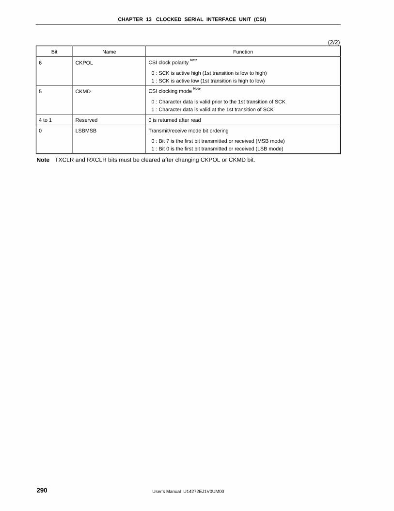
CHAPTER 13 CLOCKED SERIAL INTERFACE UNIT (CSI)
User’s Manual U14272EJ1V0UM00290
(2/2)
Bit Name Function
6 CKPOL CSI clock polarity Note
0 : SCK is active high (1st transition is low to high)
1 : SCK is active low (1st transition is high to low)
5 CKMD CSI clocking mode Note
0 : Character data is valid prior to the 1st transition of SCK
1 : Character data is valid at the 1st transition of SCK
4 to 1 Reserved 0 is returned after read
0 LSBMSB Transmit/receive mode bit ordering
0 : Bit 7 is the first bit transmitted or received (MSB mode)
1 : Bit 0 is the first bit transmitted or received (LSB mode)
Note TXCLR and RXCLR bits must be cleared after changing CKPOL or CKMD bit.
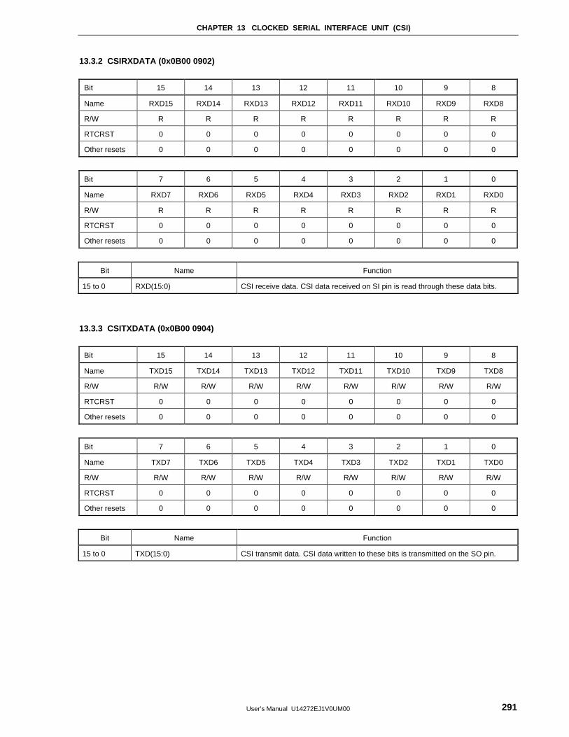
CHAPTER 13 CLOCKED SERIAL INTERFACE UNIT (CSI)
User’s Manual U14272EJ1V0UM00 291
13.3.2 CSIRXDATA (0x0B00 0902)
Bit 15 14 13 12 11 10 9 8
Name RXD15 RXD14 RXD13 RXD12 RXD11 RXD10 RXD9 RXD8
R/W R R R R R R R R
RTCRST 0 0 0 0 0 0 0 0
Other resets 0 0 0 0 0 0 0 0
Bit 7 6 5 4 3 2 1 0
Name RXD7 RXD6 RXD5 RXD4 RXD3 RXD2 RXD1 RXD0
R/W R R R R R R R R
RTCRST 0 0 0 0 0 0 0 0
Other resets 0 0 0 0 0 0 0 0
Bit Name Function
15 to 0 RXD(15:0) CSI receive data. CSI data received on SI pin is read through these data bits.
13.3.3 CSITXDATA (0x0B00 0904)
Bit 15 14 13 12 11 10 9 8
Name TXD15 TXD14 TXD13 TXD12 TXD11 TXD10 TXD9 TXD8
R/W R/W R/W R/W R/W R/W R/W R/W R/W
RTCRST 0 0 0 0 0 0 0 0
Other resets 0 0 0 0 0 0 0 0
Bit 7 6 5 4 3 2 1 0
Name TXD7 TXD6 TXD5 TXD4 TXD3 TXD2 TXD1 TXD0
R/W R/W R/W R/W R/W R/W R/W R/W R/W
RTCRST 0 0 0 0 0 0 0 0
Other resets 0 0 0 0 0 0 0 0
Bit Name Function
15 to 0 TXD(15:0) CSI transmit data. CSI data written to these bits is transmitted on the SO pin.
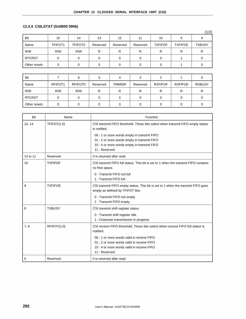
CHAPTER 13 CLOCKED SERIAL INTERFACE UNIT (CSI)
User’s Manual U14272EJ1V0UM00292
13.3.4 CSILSTAT (0x0B00 0906)
(1/2)
Bit 15 14 13 12 11 10 9 8
Name TFIFOT1 TFIFOT0 Reserved Reserved Reserved TXFIFOF TXFIFOE TXBUSY
R/W R/W R/W R R R R R R
RTCRST 0 0 0 0 0 0 1 0
Other resets 0 0 0 0 0 0 1 0
Bit 7 6 5 4 3 2 1 0
Name RFIFOT1 RFIFOT0 Reserved FRMDIR Reserved RXFIFOF RXFIFOE RXBUSY
R/W R/W R/W R R R R R R
RTCRST 0 0 0 0 0 0 0 0
Other resets 0 0 0 0 0 0 0 0
Bit Name Function
15, 14 TFIFOT(1:0) CSI transmit FIFO threshold. These bits select when transmit FIFO empty status
is notified.
00 : 1 or more words empty in transmit FIFO
01 : 2 or more words empty in transmit FIFO
10 : 4 or more words empty in transmit FIFO
11 : Reserved
13 to 11 Reserved 0 is returned after read
10 TXFIFOF CSI transmit FIFO full status. This bit is set to 1 when the transmit FIFO contains
no free space.
0 : Transmit FIFO not full
1 : Transmit FIFO full
9 TXFIFOE CSI transmit FIFO empty status. This bit is set to 1 when the transmit FIFO goes
empty as defined by TFIFOT bits.
0 : Transmit FIFO not empty
1 : Transmit FIFO empty
8 TXBUSY CSI transmit shift register status
0 : Transmit shift register idle
1 : Character transmission in progress
7, 6 RFIFOT(1:0) CSI receive FIFO threshold. These bits select when receive FIFO full status is
notified.
00 : 1 or more words valid in receive FIFO
01 : 2 or more words valid in receive FIFO
10 : 4 or more words valid in receive FIFO
11 : Reserved
5 Reserved 0 is returned after read
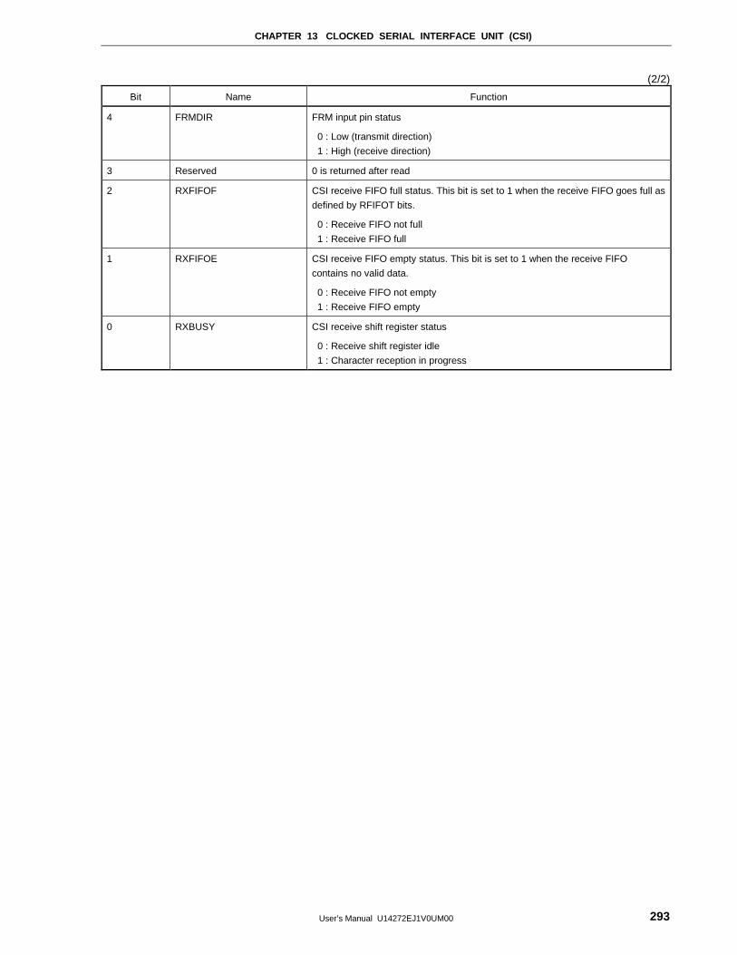
CHAPTER 13 CLOCKED SERIAL INTERFACE UNIT (CSI)
User’s Manual U14272EJ1V0UM00 293
(2/2)
Bit Name Function
4 FRMDIR FRM input pin status
0 : Low (transmit direction)
1 : High (receive direction)
3 Reserved 0 is returned after read
2 RXFIFOF CSI receive FIFO full status. This bit is set to 1 when the receive FIFO goes full as
defined by RFIFOT bits.
0 : Receive FIFO not full
1 : Receive FIFO full
1 RXFIFOE CSI receive FIFO empty status. This bit is set to 1 when the receive FIFO
contains no valid data.
0 : Receive FIFO not empty
1 : Receive FIFO empty
0 RXBUSY CSI receive shift register status
0 : Receive shift register idle
1 : Character reception in progress
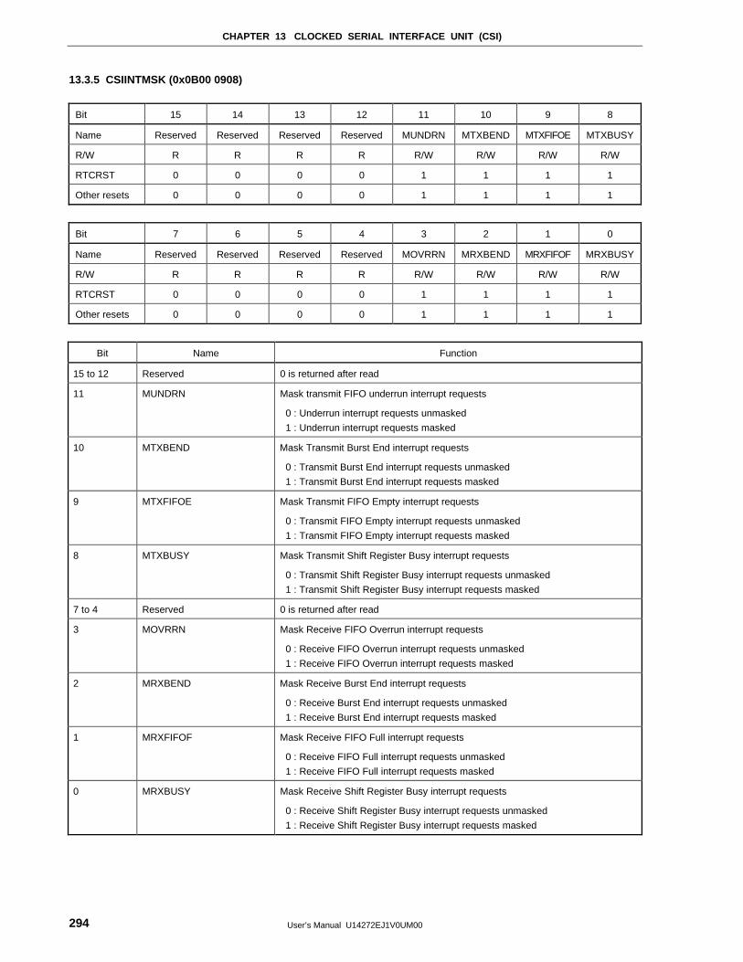
CHAPTER 13 CLOCKED SERIAL INTERFACE UNIT (CSI)
User’s Manual U14272EJ1V0UM00294
13.3.5 CSIINTMSK (0x0B00 0908)
Bit 15 14 13 12 11 10 9 8
Name Reserved Reserved Reserved Reserved MUNDRN MTXBEND MTXFIFOE MTXBUSY
R/W R R R R R/W R/W R/W R/W
RTCRST 0 0 0 0 1 1 1 1
Other resets 0 0 0 0 1 1 1 1
Bit 7 6 5 4 3 2 1 0
Name Reserved Reserved Reserved Reserved MOVRRN MRXBEND MRXFIFOF MRXBUSY
R/W R R R R R/W R/W R/W R/W
RTCRST 0 0 0 0 1 1 1 1
Other resets 0 0 0 0 1 1 1 1
Bit Name Function
15 to 12 Reserved 0 is returned after read
11 MUNDRN Mask transmit FIFO underrun interrupt requests
0 : Underrun interrupt requests unmasked
1 : Underrun interrupt requests masked
10 MTXBEND Mask Transmit Burst End interrupt requests
0 : Transmit Burst End interrupt requests unmasked
1 : Transmit Burst End interrupt requests masked
9 MTXFIFOE Mask Transmit FIFO Empty interrupt requests
0 : Transmit FIFO Empty interrupt requests unmasked
1 : Transmit FIFO Empty interrupt requests masked
8 MTXBUSY Mask Transmit Shift Register Busy interrupt requests
0 : Transmit Shift Register Busy interrupt requests unmasked
1 : Transmit Shift Register Busy interrupt requests masked
7 to 4 Reserved 0 is returned after read
3 MOVRRN Mask Receive FIFO Overrun interrupt requests
0 : Receive FIFO Overrun interrupt requests unmasked
1 : Receive FIFO Overrun interrupt requests masked
2 MRXBEND Mask Receive Burst End interrupt requests
0 : Receive Burst End interrupt requests unmasked
1 : Receive Burst End interrupt requests masked
1 MRXFIFOF Mask Receive FIFO Full interrupt requests
0 : Receive FIFO Full interrupt requests unmasked
1 : Receive FIFO Full interrupt requests masked
0 MRXBUSY Mask Receive Shift Register Busy interrupt requests
0 : Receive Shift Register Busy interrupt requests unmasked
1 : Receive Shift Register Busy interrupt requests masked
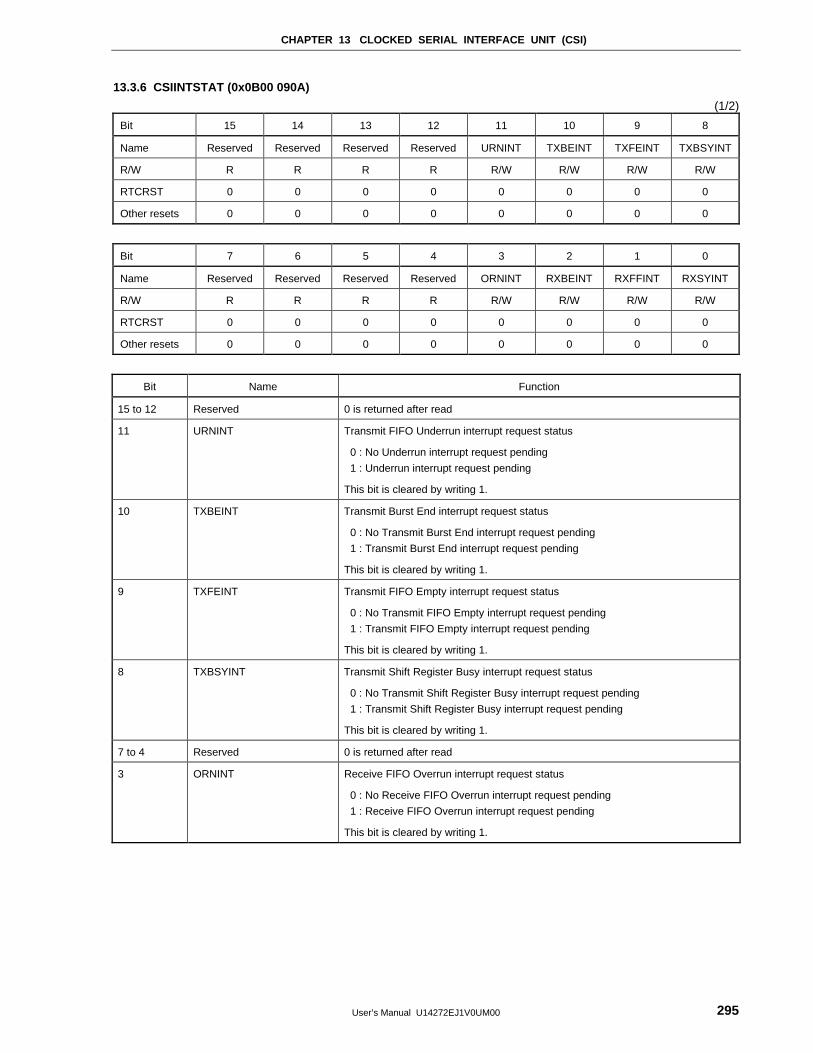
CHAPTER 13 CLOCKED SERIAL INTERFACE UNIT (CSI)
User’s Manual U14272EJ1V0UM00 295
13.3.6 CSIINTSTAT (0x0B00 090A)
(1/2)
Bit 15 14 13 12 11 10 9 8
Name Reserved Reserved Reserved Reserved URNINT TXBEINT TXFEINT TXBSYINT
R/W R R R R R/W R/W R/W R/W
RTCRST 0 0 0 0 0 0 0 0
Other resets 0 0 0 0 0 0 0 0
Bit 7 6 5 4 3 2 1 0
Name Reserved Reserved Reserved Reserved ORNINT RXBEINT RXFFINT RXSYINT
R/W R R R R R/W R/W R/W R/W
RTCRST 0 0 0 0 0 0 0 0
Other resets 0 0 0 0 0 0 0 0
Bit Name Function
15 to 12 Reserved 0 is returned after read
11 URNINT Transmit FIFO Underrun interrupt request status
0 : No Underrun interrupt request pending
1 : Underrun interrupt request pending
This bit is cleared by writing 1.
10 TXBEINT Transmit Burst End interrupt request status
0 : No Transmit Burst End interrupt request pending
1 : Transmit Burst End interrupt request pending
This bit is cleared by writing 1.
9 TXFEINT Transmit FIFO Empty interrupt request status
0 : No Transmit FIFO Empty interrupt request pending
1 : Transmit FIFO Empty interrupt request pending
This bit is cleared by writing 1.
8 TXBSYINT Transmit Shift Register Busy interrupt request status
0 : No Transmit Shift Register Busy interrupt request pending
1 : Transmit Shift Register Busy interrupt request pending
This bit is cleared by writing 1.
7 to 4 Reserved 0 is returned after read
3 ORNINT Receive FIFO Overrun interrupt request status
0 : No Receive FIFO Overrun interrupt request pending
1 : Receive FIFO Overrun interrupt request pending
This bit is cleared by writing 1.
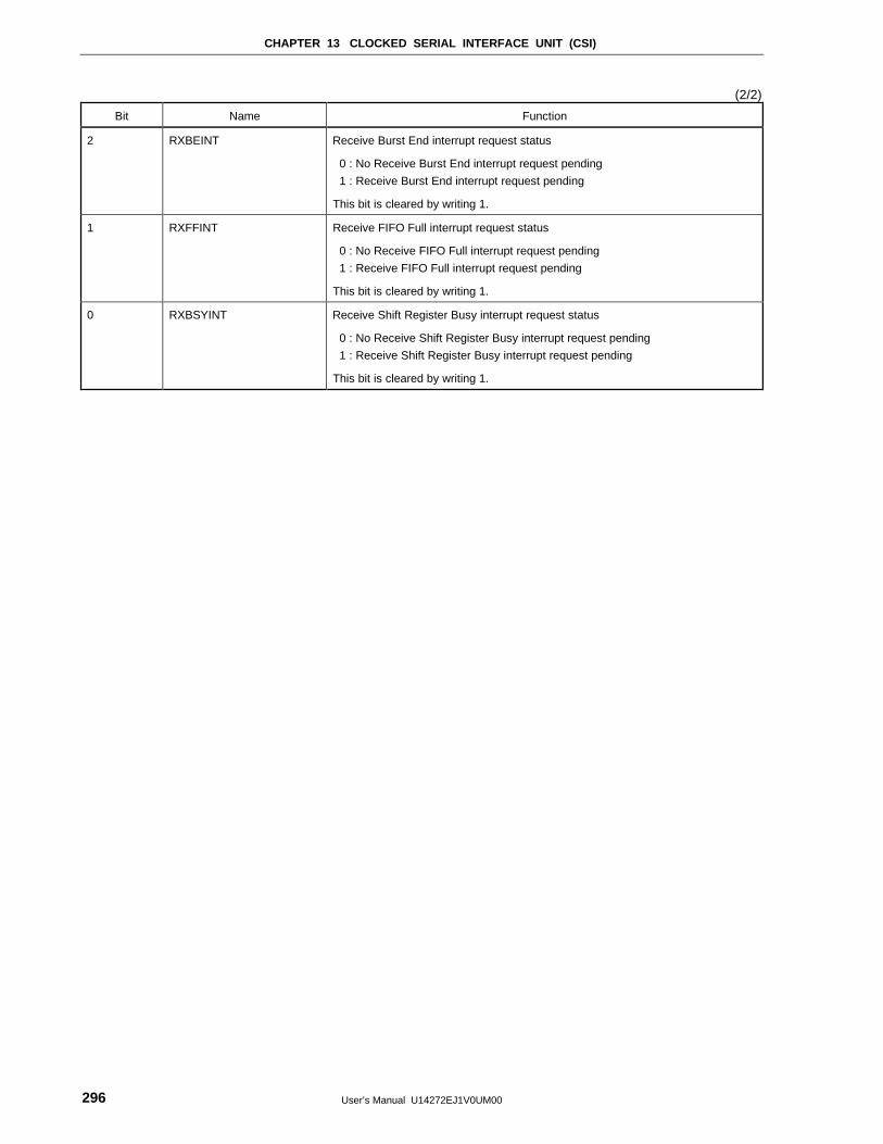
CHAPTER 13 CLOCKED SERIAL INTERFACE UNIT (CSI)
User’s Manual U14272EJ1V0UM00296
(2/2)
Bit Name Function
2 RXBEINT Receive Burst End interrupt request status
0 : No Receive Burst End interrupt request pending
1 : Receive Burst End interrupt request pending
This bit is cleared by writing 1.
1 RXFFINT Receive FIFO Full interrupt request status
0 : No Receive FIFO Full interrupt request pending
1 : Receive FIFO Full interrupt request pending
This bit is cleared by writing 1.
0 RXBSYINT Receive Shift Register Busy interrupt request status
0 : No Receive Shift Register Busy interrupt request pending
1 : Receive Shift Register Busy interrupt request pending
This bit is cleared by writing 1.
CHAPTER 13 CLOCKED SERIAL INTERFACE UNIT (CSI)
User’s Manual U14272EJ1V0UM00 297
13.3.7 CSITXBLEN (0x0B00 090C)
Bit 15 14 13 12 11 10 9 8
Name TXBLN15 TXBLN14 TXBLN13 TXBLN12 TXBLN11 TXBLN10 TXBLN9 TXBLN8
R/W R/W R/W R/W R/W R/W R/W R/W R/W
RTCRST 0 0 0 0 0 0 0 0
Other resets 0 0 0 0 0 0 0 0
Bit 7 6 5 4 3 2 1 0
Name TXBLN7 TXBLN6 TXBLN5 TXBLN4 TXBLN3 TXBLN2 TXBLN1 TXBLN0
R/W R/W R/W R/W R/W R/W R/W R/W R/W
RTCRST 0 0 0 0 0 0 0 0
Other resets 0 0 0 0 0 0 0 0
Bit Name Function
15 to 0 TXBLN(15:0) Transmit burst length. These bits determine the number of bits transmitted during
one burst cycle.
0x0000 : Reserved
0x0001 : 1 bit
0x0002 : 2 bits
:
:
0x00FD : 253 bits
0x00FE : 254 bits
0x00FF : 255 bits
:
:
0xFFFD : 65533 bits
0xFFFE : 65534 bits
0xFFFF : 65535 bits
CHAPTER 13 CLOCKED SERIAL INTERFACE UNIT (CSI)
User’s Manual U14272EJ1V0UM00298
13.3.8 CSIRXBLEN (0x0B00 090E)
Bit 15 14 13 12 11 10 9 8
Name RXBLN15 RXBLN14 RXBLN13 RXBLN12 RXBLN11 RXBLN10 RXBLN9 RXBLN8
R/W R/W R/W R/W R/W R/W R/W R/W R/W
RTCRST 0 0 0 0 0 0 0 0
Other resets 0 0 0 0 0 0 0 0
Bit 7 6 5 4 3 2 1 0
Name RXBLN7 RXBLN6 RXBLN5 RXBLN4 RXBLN3 RXBLN2 RXBLN1 RXBLN0
R/W R/W R/W R/W R/W R/W R/W R/W R/W
RTCRST 0 0 0 0 0 0 0 0
Other resets 0 0 0 0 0 0 0 0
Bit Name Function
15 to 0 RXBLN(15:0) Receive burst length. These bits determine the number of bits received during one
burst cycle.
0x0000 : Reserved
0x0001 : 1 bit
0x0002 : 2 bits
:
:
0x00FD : 253 bits
0x00FE : 254 bits
0x00FF : 255 bits
:
:
0xFFFD : 65533 bits
0xFFFE : 65534 bits
0xFFFF : 65535 bits
User’s Manual U14272EJ1V0UM00 299
CHAPTER 14 INTERRUPT CONTROL UNIT (ICU)
14.1 Overview
The ICU collects interrupt requests from the various on-chip peripheral units and transfers them with internal
interrupt request signals (Int0, Int1, Int2, Int3, and NMI) to the CPU core.
The signals used to notice interrupt requests to the CPU are as below.
NMI: battint_intr only. Switching between NMI and Int0 is enabled according to NMIREG register’s settings.
Because NMI’s interrupt masking cannot be controlled by means of software, switch to Int0 to mask
battint_intr.
Int3: Not used (fixed to 1 (inactive))
Int2: rtc_long2_intr only (RTCLong2 Timer)
Int1: rtc_long1_intr only (RTCLong1 Timer)
Int0: All other interrupts. For details of the interrupt sources, see 14.2 Register Set .
How an interrupt request is notified to the CPU core is shown below.
If an interrupt request occurs in the peripheral units, the corresponding bit in the interrupt indication register of
Level 2 (xxxINTREG) is set to 1. The interrupt indication register is ANDed bit-wise with the corresponding interrupt
mask register of Level 2 (MxxxINTREG). If the occurred interrupt request is enabled (set to 1) in the mask register,
the interrupt request is notified to the interrupt indication register of Level 1 (SYSINTREG) and the corresponding bit
is set to 1. At this time, the interrupt requests from the same register of Level 2 are notified to the SYSINTREG as a
single interrupt request.
Interrupt requests from some units directly set their corresponding bits in the SYSINTREG.
The SYSINTREG is ANDed bit-wise with the interrupt mask register of Level 1 (MSYSINTREG). If the interrupt
request is enabled by MSYSINTREG (set to 1), a corresponding interrupt request signal is output from the ICU to the
CPU core. battintr is connected to the NMI or Int0 signal of the CPU core (selected by setting of NMIREG). rtc_long
signals are connected to the Int2 or Int1 signal of the CPU core. The other interrupt requests are connected to the
Int0 signal of the CPU core as a single interrupt request.
The following figure shows an outline of interrupt control in the ICU.
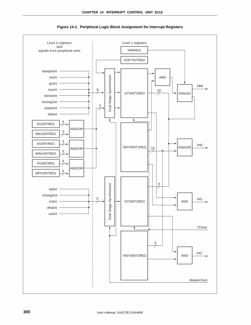
CHAPTER 14 INTERRUPT CONTROL UNIT (ICU)
User’s Manual U14272EJ1V0UM00300
Figure 14-1. Peripheral Logic Block Assignment for Interrupt Registers
ecuint
NMIREG
AND
AND/OR
AND/OR
siuint
etimerint
dozepiuint
giuint
MPIUINTREG
PIUINTREG
MAIUINTREG
AIUINTREG
dmaint
Dua
l Sta
ge S
ynch
roni
zer
Int2
Int1
NMI
Int0MSYSINT1REG
MSYSINT2REG
battint
powerint
rtclong2int
rtclong1int
csuint
SYSINT1REG
SYSINT2REGlcdint
ledint
AND/OR
MKIUINTREG
KIUINTREG
Dua
l Sta
ge S
ynch
roni
zer
SOFTINTREG
Selector
AND/OR
AND
TClock
MasterClock
3
5
AND
10
10
4
4
Level 2 registersand
signals from peripheral units
Level 1 registers
8
3
3
3
3
6
6
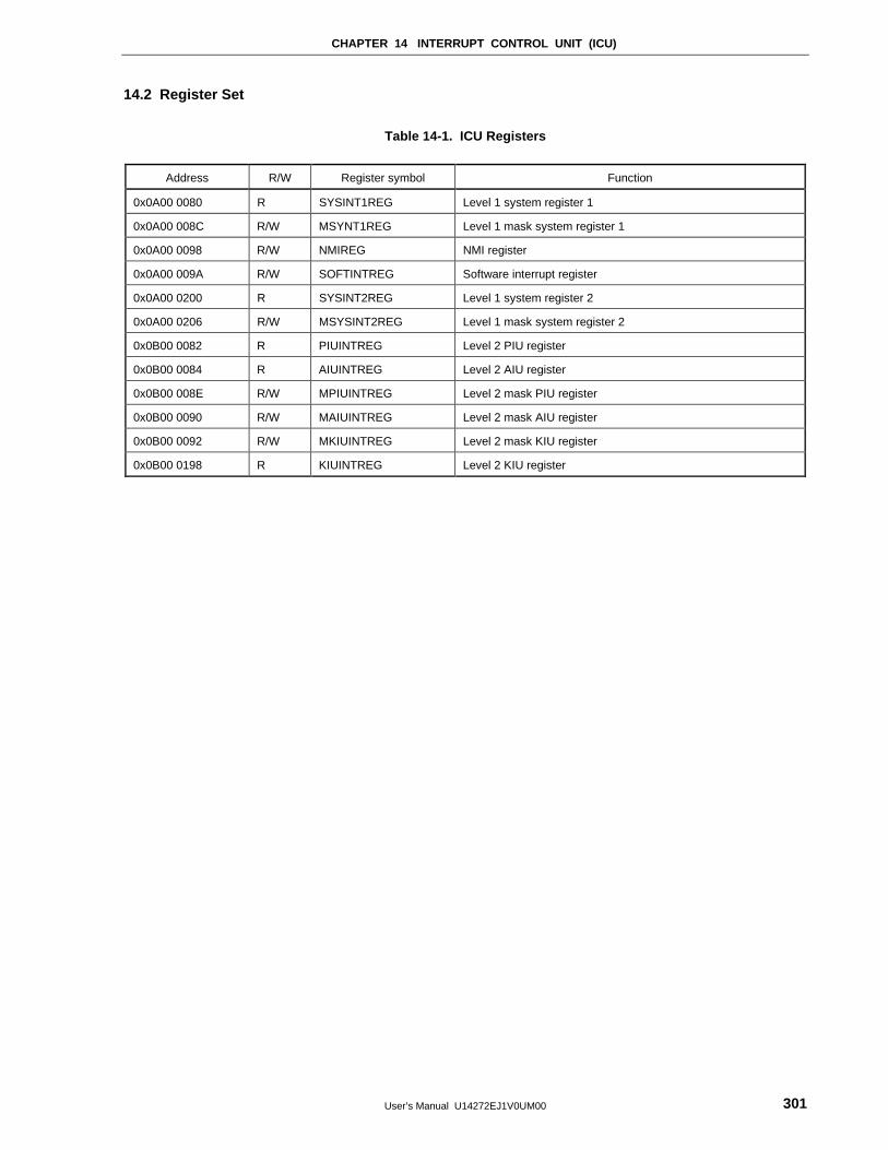
CHAPTER 14 INTERRUPT CONTROL UNIT (ICU)
User’s Manual U14272EJ1V0UM00 301
14.2 Register Set
Table 14-1. ICU Registers
Address R/W Register symbol Function
0x0A00 0080 R SYSINT1REG Level 1 system register 1
0x0A00 008C R/W MSYNT1REG Level 1 mask system register 1
0x0A00 0098 R/W NMIREG NMI register
0x0A00 009A R/W SOFTINTREG Software interrupt register
0x0A00 0200 R SYSINT2REG Level 1 system register 2
0x0A00 0206 R/W MSYSINT2REG Level 1 mask system register 2
0x0B00 0082 R PIUINTREG Level 2 PIU register
0x0B00 0084 R AIUINTREG Level 2 AIU register
0x0B00 008E R/W MPIUINTREG Level 2 mask PIU register
0x0B00 0090 R/W MAIUINTREG Level 2 mask AIU register
0x0B00 0092 R/W MKIUINTREG Level 2 mask KIU register
0x0B00 0198 R KIUINTREG Level 2 KIU register

CHAPTER 14 INTERRUPT CONTROL UNIT (ICU)
User’s Manual U14272EJ1V0UM00302
14.2.1 SYSINT1REG (0x0A00 0080)
(1/2)
Bit 15 14 13 12 11 10 9 8
Name Reserved Reserved DOZEPIU
INTR
Reserved SOFTINTR Reserved SIUINTR GIUINTR
R/W R R R R R R R R
RTCRST 0 0 0 0 0 0 0 0
Other resets 0 0 0 0 0 0 0 0
Bit 7 6 5 4 3 2 1 0
Name KIUINTR AIUINTR PIUINTR Reserved ETIMER
INTR
RTCL1
INTR
POWER
INTR
BATINTR
R/W R R R R R R R R
RTCRST 0 0 0 0 0 0 0 0
Other resets 0 0 0 0 0 0 0 0
Bit Name Function
15, 14 Reserved 0 is returned when read
13 DOZEPIUINTR PIU interrupt request during Suspend mode
0 : Not occurred
1 : Occurred
12 Reserved 0 is returned when read
11 SOFTINTR Software interrupt request
0 : Not occurred
1 : Occurred
10 Reserved 0 is returned when read
9 SIUINTR SIU interrupt request
0 : Not occurred
1 : Occurred
8 GIUINTR GIU interrupt request
0 : Not occurred
1 : Occurred
7 KIUINTR KIU interrupt request
0 : Not occurred
1 : Occurred
6 AIUINTR AIU interrupt request
0 : Not occurred
1 : Occurred
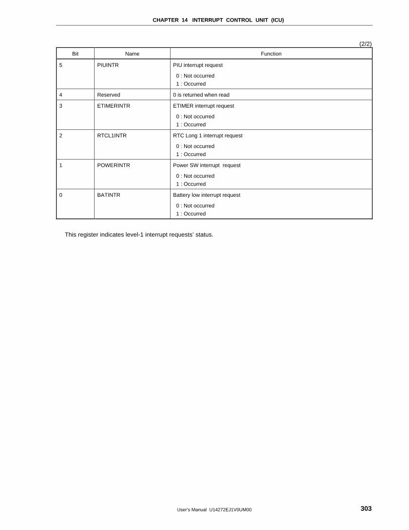
CHAPTER 14 INTERRUPT CONTROL UNIT (ICU)
User’s Manual U14272EJ1V0UM00 303
(2/2)
Bit Name Function
5 PIUINTR PIU interrupt request
0 : Not occurred
1 : Occurred
4 Reserved 0 is returned when read
3 ETIMERINTR ETIMER interrupt request
0 : Not occurred
1 : Occurred
2 RTCL1INTR RTC Long 1 interrupt request
0 : Not occurred
1 : Occurred
1 POWERINTR Power SW interrupt request
0 : Not occurred
1 : Occurred
0 BATINTR Battery low interrupt request
0 : Not occurred
1 : Occurred
This register indicates level-1 interrupt requests’ status.
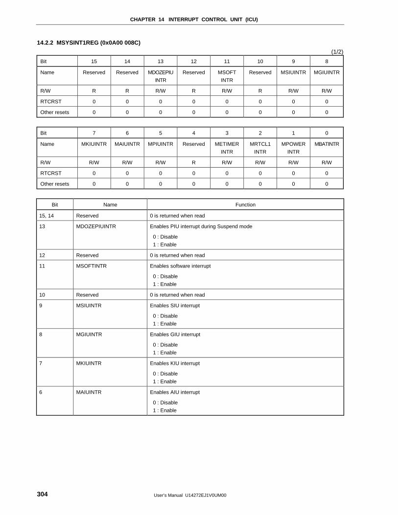
CHAPTER 14 INTERRUPT CONTROL UNIT (ICU)
User’s Manual U14272EJ1V0UM00304
14.2.2 MSYSINT1REG (0x0A00 008C)
(1/2)
Bit 15 14 13 12 11 10 9 8
Name Reserved Reserved MDOZEPIU
INTR
Reserved MSOFT
INTR
Reserved MSIUINTR MGIUINTR
R/W R R R/W R R/W R R/W R/W
RTCRST 0 0 0 0 0 0 0 0
Other resets 0 0 0 0 0 0 0 0
Bit 7 6 5 4 3 2 1 0
Name MKIUINTR MAIUINTR MPIUINTR Reserved METIMER
INTR
MRTCL1
INTR
MPOWER
INTR
MBATINTR
R/W R/W R/W R/W R R/W R/W R/W R/W
RTCRST 0 0 0 0 0 0 0 0
Other resets 0 0 0 0 0 0 0 0
Bit Name Function
15, 14 Reserved 0 is returned when read
13 MDOZEPIUINTR Enables PIU interrupt during Suspend mode
0 : Disable
1 : Enable
12 Reserved 0 is returned when read
11 MSOFTINTR Enables software interrupt
0 : Disable
1 : Enable
10 Reserved 0 is returned when read
9 MSIUINTR Enables SIU interrupt
0 : Disable
1 : Enable
8 MGIUINTR Enables GIU interrupt
0 : Disable
1 : Enable
7 MKIUINTR Enables KIU interrupt
0 : Disable
1 : Enable
6 MAIUINTR Enables AIU interrupt
0 : Disable
1 : Enable
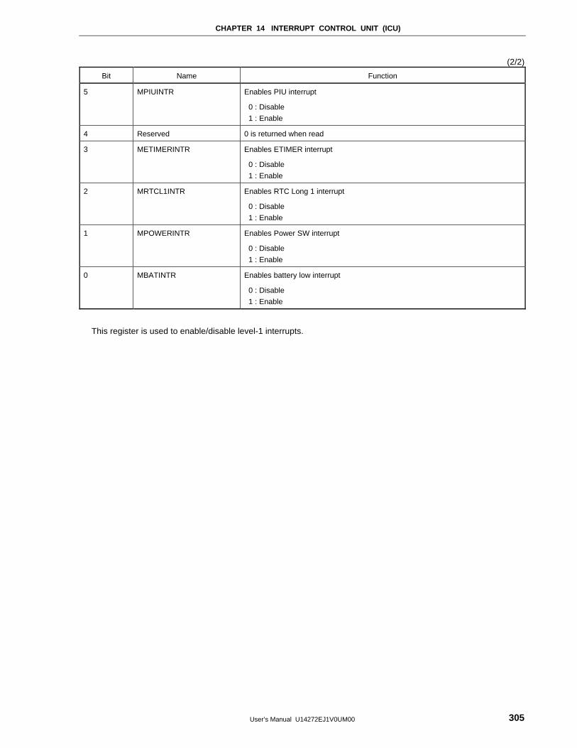
CHAPTER 14 INTERRUPT CONTROL UNIT (ICU)
User’s Manual U14272EJ1V0UM00 305
(2/2)
Bit Name Function
5 MPIUINTR Enables PIU interrupt
0 : Disable
1 : Enable
4 Reserved 0 is returned when read
3 METIMERINTR Enables ETIMER interrupt
0 : Disable
1 : Enable
2 MRTCL1INTR Enables RTC Long 1 interrupt
0 : Disable
1 : Enable
1 MPOWERINTR Enables Power SW interrupt
0 : Disable
1 : Enable
0 MBATINTR Enables battery low interrupt
0 : Disable
1 : Enable
This register is used to enable/disable level-1 interrupts.
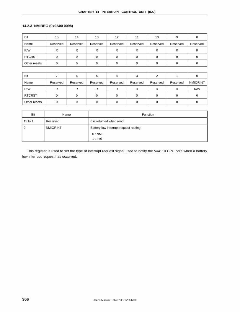
CHAPTER 14 INTERRUPT CONTROL UNIT (ICU)
User’s Manual U14272EJ1V0UM00306
14.2.3 NMIREG (0x0A00 0098)
Bit 15 14 13 12 11 10 9 8
Name Reserved Reserved Reserved Reserved Reserved Reserved Reserved Reserved
R/W R R R R R R R R
RTCRST 0 0 0 0 0 0 0 0
Other resets 0 0 0 0 0 0 0 0
Bit 7 6 5 4 3 2 1 0
Name Reserved Reserved Reserved Reserved Reserved Reserved Reserved NMIORINT
R/W R R R R R R R R/W
RTCRST 0 0 0 0 0 0 0 0
Other resets 0 0 0 0 0 0 0 0
Bit Name Function
15 to 1 Reserved 0 is returned when read
0 NMIORINT Battery low interrupt request routing
0 : NMI
1 : Int0
This register is used to set the type of interrupt request signal used to notify the VR4110 CPU core when a battery
low interrupt request has occurred.
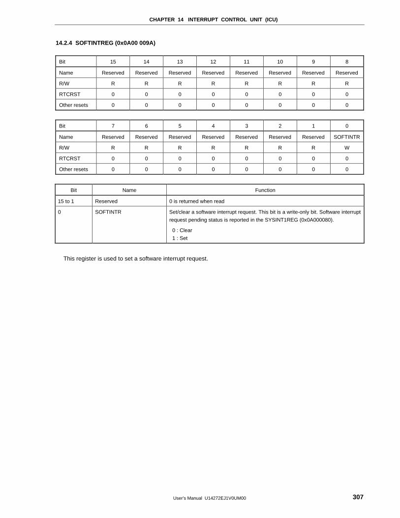
CHAPTER 14 INTERRUPT CONTROL UNIT (ICU)
User’s Manual U14272EJ1V0UM00 307
14.2.4 SOFTINTREG (0x0A00 009A)
Bit 15 14 13 12 11 10 9 8
Name Reserved Reserved Reserved Reserved Reserved Reserved Reserved Reserved
R/W R R R R R R R R
RTCRST 0 0 0 0 0 0 0 0
Other resets 0 0 0 0 0 0 0 0
Bit 7 6 5 4 3 2 1 0
Name Reserved Reserved Reserved Reserved Reserved Reserved Reserved SOFTINTR
R/W R R R R R R R W
RTCRST 0 0 0 0 0 0 0 0
Other resets 0 0 0 0 0 0 0 0
Bit Name Function
15 to 1 Reserved 0 is returned when read
0 SOFTINTR Set/clear a software interrupt request. This bit is a write-only bit. Software interrupt
request pending status is reported in the SYSINT1REG (0x0A000080).
0 : Clear
1 : Set
This register is used to set a software interrupt request.
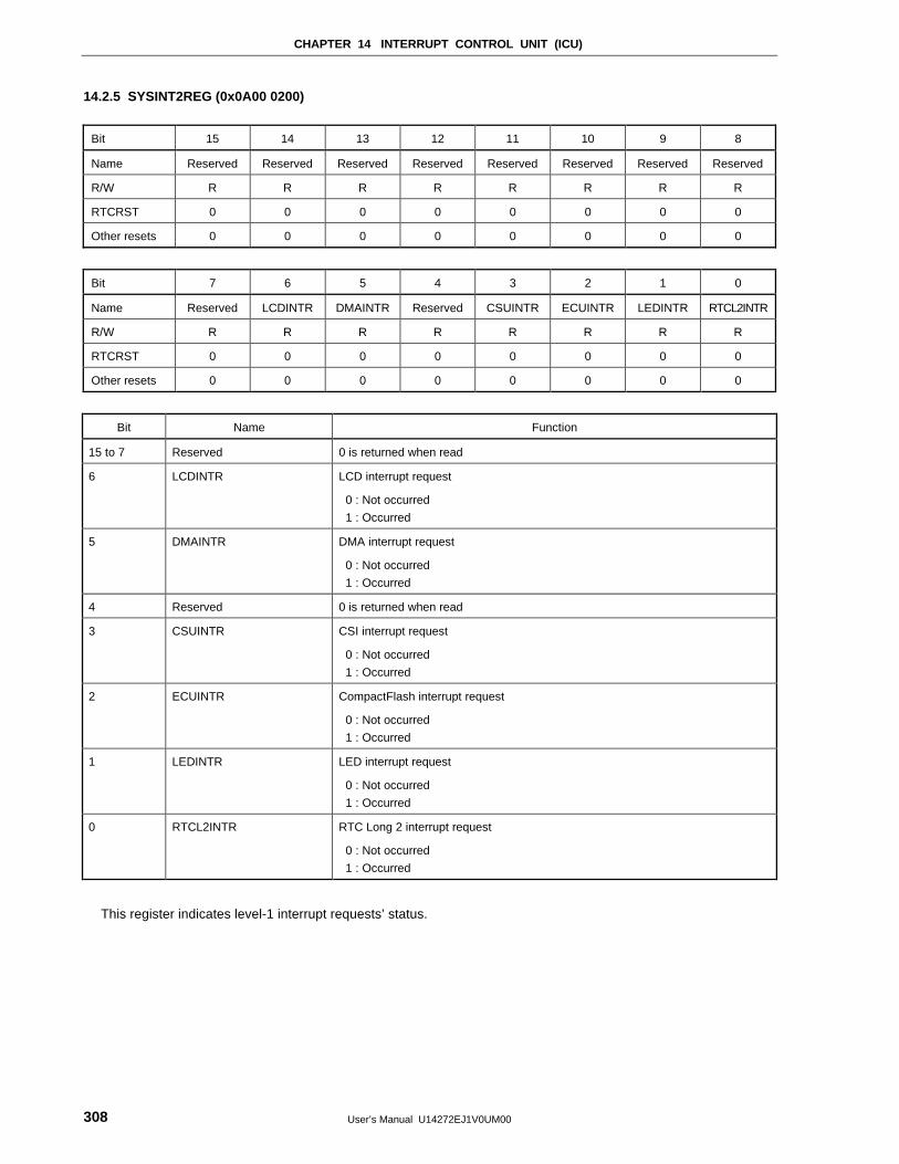
CHAPTER 14 INTERRUPT CONTROL UNIT (ICU)
User’s Manual U14272EJ1V0UM00308
14.2.5 SYSINT2REG (0x0A00 0200)
Bit 15 14 13 12 11 10 9 8
Name Reserved Reserved Reserved Reserved Reserved Reserved Reserved Reserved
R/W R R R R R R R R
RTCRST 0 0 0 0 0 0 0 0
Other resets 0 0 0 0 0 0 0 0
Bit 7 6 5 4 3 2 1 0
Name Reserved LCDINTR DMAINTR Reserved CSUINTR ECUINTR LEDINTR RTCL2INTR
R/W R R R R R R R R
RTCRST 0 0 0 0 0 0 0 0
Other resets 0 0 0 0 0 0 0 0
Bit Name Function
15 to 7 Reserved 0 is returned when read
6 LCDINTR LCD interrupt request
0 : Not occurred
1 : Occurred
5 DMAINTR DMA interrupt request
0 : Not occurred
1 : Occurred
4 Reserved 0 is returned when read
3 CSUINTR CSI interrupt request
0 : Not occurred
1 : Occurred
2 ECUINTR CompactFlash interrupt request
0 : Not occurred
1 : Occurred
1 LEDINTR LED interrupt request
0 : Not occurred
1 : Occurred
0 RTCL2INTR RTC Long 2 interrupt request
0 : Not occurred
1 : Occurred
This register indicates level-1 interrupt requests’ status.
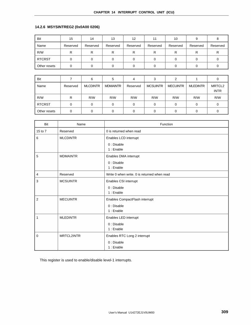
CHAPTER 14 INTERRUPT CONTROL UNIT (ICU)
User’s Manual U14272EJ1V0UM00 309
14.2.6 MSYSINTREG2 (0x0A00 0206)
Bit 15 14 13 12 11 10 9 8
Name Reserved Reserved Reserved Reserved Reserved Reserved Reserved Reserved
R/W R R R R R R R R
RTCRST 0 0 0 0 0 0 0 0
Other resets 0 0 0 0 0 0 0 0
Bit 7 6 5 4 3 2 1 0
Name Reserved MLCDINTR MDMAINTR Reserved MCSUINTR MECUINTR MLEDINTR MRTCL2
INTR
R/W R R/W R/W R/W R/W R/W R/W R/W
RTCRST 0 0 0 0 0 0 0 0
Other resets 0 0 0 0 0 0 0 0
Bit Name Function
15 to 7 Reserved 0 is returned when read
6 MLCDINTR Enables LCD interrupt
0 : Disable
1 : Enable
5 MDMAINTR Enables DMA interrupt
0 : Disable
1 : Enable
4 Reserved Write 0 when write. 0 is returned when read
3 MCSUINTR Enables CSI interrupt
0 : Disable
1 : Enable
2 MECUINTR Enables CompactFlash interrupt
0 : Disable
1 : Enable
1 MLEDINTR Enables LED interrupt
0 : Disable
1 : Enable
0 MRTCL2INTR Enables RTC Long 2 interrupt
0 : Disable
1 : Enable
This register is used to enable/disable level-1 interrupts.
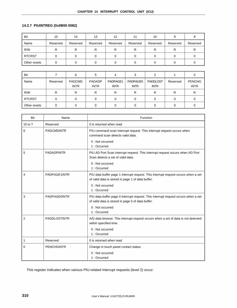
CHAPTER 14 INTERRUPT CONTROL UNIT (ICU)
User’s Manual U14272EJ1V0UM00310
14.2.7 PIUINTREG (0x0B00 0082)
Bit 15 14 13 12 11 10 9 8
Name Reserved Reserved Reserved Reserved Reserved Reserved Reserved Reserved
R/W R R R R R R R R
RTCRST 0 0 0 0 0 0 0 0
Other resets 0 0 0 0 0 0 0 0
Bit 7 6 5 4 3 2 1 0
Name Reserved PADCMD
INTR
PADADP
INTR
PADPAGE1
INTR
PADPAGE0
INTR
PADDLOST
INTR
Reserved PENCHG
INTR
R/W R R R R R R R R
RTCRST 0 0 0 0 0 0 0 0
Other resets 0 0 0 0 0 0 0 0
Bit Name Function
15 to 7 Reserved 0 is returned when read
6 PADCMDINTR PIU command scan interrupt request. This interrupt request occurs when
command scan detects valid data.
0 : Not occurred
1 : Occurred
5 PADADPINTR PIU AD Port Scan interrupt request. This interrupt request occurs when AD Port
Scan detects a set of valid data.
0 : Not occurred
1 : Occurred
4 PADPAGE1INTR PIU data buffer page 1 interrupt request. This interrupt request occurs when a set
of valid data is stored in page 1 of data buffer.
0 : Not occurred
1 : Occurred
3 PADPAGE0INTR PIU data buffer page 0 interrupt request. This interrupt request occurs when a set
of valid data is stored in page 0 of data buffer.
0 : Not occurred
1 : Occurred
2 PADDLOSTINTR A/D data timeout. This interrupt request occurs when a set of data is not detected
within specified time.
0 : Not occurred
1 : Occurred
1 Reserved 0 is returned when read
0 PENCHGINTR Change in touch panel contact status
0 : Not occurred
1 : Occurred
This register indicates when various PIU-related interrupt requests (level 2) occur.
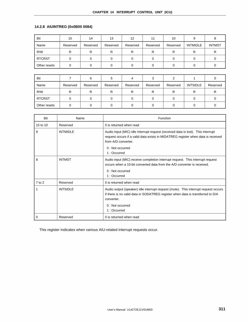
CHAPTER 14 INTERRUPT CONTROL UNIT (ICU)
User’s Manual U14272EJ1V0UM00 311
14.2.8 AIUINTREG (0x0B00 0084)
Bit 15 14 13 12 11 10 9 8
Name Reserved Reserved Reserved Reserved Reserved Reserved INTMIDLE INTMST
R/W R R R R R R R R
RTCRST 0 0 0 0 0 0 0 0
Other resets 0 0 0 0 0 0 0 0
Bit 7 6 5 4 3 2 1 0
Name Reserved Reserved Reserved Reserved Reserved Reserved INTSIDLE Reserved
R/W R R R R R R R R
RTCRST 0 0 0 0 0 0 0 0
Other resets 0 0 0 0 0 0 0 0
Bit Name Function
15 to 10 Reserved 0 is returned when read
9 INTMIDLE Audio input (MIC) idle interrupt request (received data is lost). This interrupt
request occurs if a valid data exists in MIDATREG register when data is received
from A/D converter.
0 : Not occurred
1 : Occurred
8 INTMST Audio input (MIC) receive completion interrupt request. This interrupt request
occurs when a 10-bit converted data from the A/D converter is received.
0 : Not occurred
1 : Occurred
7 to 2 Reserved 0 is returned when read
1 INTSIDLE Audio output (speaker) idle interrupt request (mute). This interrupt request occurs
if there is no valid data in SODATREG register when data is transferred to D/A
converter.
0 : Not occurred
1 : Occurred
0 Reserved 0 is returned when read
This register indicates when various AIU-related interrupt requests occur.
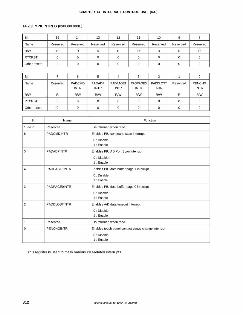
CHAPTER 14 INTERRUPT CONTROL UNIT (ICU)
User’s Manual U14272EJ1V0UM00312
14.2.9 MPIUINTREG (0x0B00 008E)
Bit 15 14 13 12 11 10 9 8
Name Reserved Reserved Reserved Reserved Reserved Reserved Reserved Reserved
R/W R R R R R R R R
RTCRST 0 0 0 0 0 0 0 0
Other resets 0 0 0 0 0 0 0 0
Bit 7 6 5 4 3 2 1 0
Name Reserved PADCMD
INTR
PADADP
INTR
PADPAGE1
INTR
PADPAGE0
INTR
PADDLOST
INTR
Reserved PENCHG
INTR
R/W R R/W R/W R/W R/W R/W R R/W
RTCRST 0 0 0 0 0 0 0 0
Other resets 0 0 0 0 0 0 0 0
Bit Name Function
15 to 7 Reserved 0 is returned when read
6 PADCMDINTR Enables PIU command scan interrupt
0 : Disable
1 : Enable
5 PADADPINTR Enables PIU AD Port Scan interrupt
0 : Disable
1 : Enable
4 PADPAGE1INTR Enables PIU data buffer page 1 interrupt
0 : Disable
1 : Enable
3 PADPAGE0INTR Enables PIU data buffer page 0 interrupt
0 : Disable
1 : Enable
2 PADDLOSTINTR Enables A/D data timeout interrupt
0 : Disable
1 : Enable
1 Reserved 0 is returned when read
0 PENCHGINTR Enables touch panel contact status change interrupt
0 : Disable
1 : Enable
This register is used to mask various PIU-related interrupts.
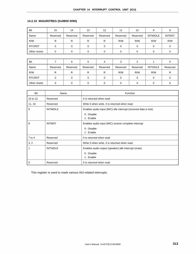
CHAPTER 14 INTERRUPT CONTROL UNIT (ICU)
User’s Manual U14272EJ1V0UM00 313
14.2.10 MAIUINTREG (0x0B00 0090)
Bit 15 14 13 12 11 10 9 8
Name Reserved Reserved Reserved Reserved Reserved Reserved INTMIDLE INTMST
R/W R R R R R/W R/W R/W R/W
RTCRST 0 0 0 0 0 0 0 0
Other resets 0 0 0 0 0 0 0 0
Bit 7 6 5 4 3 2 1 0
Name Reserved Reserved Reserved Reserved Reserved Reserved INTSIDLE Reserved
R/W R R R R R/W R/W R/W R
RTCRST 0 0 0 0 0 0 0 0
Other resets 0 0 0 0 0 0 0 0
Bit Name Function
15 to 12 Reserved 0 is returned when read
11, 10 Reserved Write 0 when write. 0 is returned when read.
9 INTMIDLE Enables audio input (MIC) idle interrupt (received data is lost)
0 : Disable
1 : Enable
8 INTMST Enables audio input (MIC) receive complete interrupt
0 : Disable
1 : Enable
7 to 4 Reserved 0 is returned when read
3, 2 Reserved Write 0 when write. 0 is returned when read.
1 INTSIDLE Enables audio output (speaker) idle interrupt (mute)
0 : Disable
1 : Enable
0 Reserved 0 is returned when read
This register is used to mask various AIU-related interrupts.
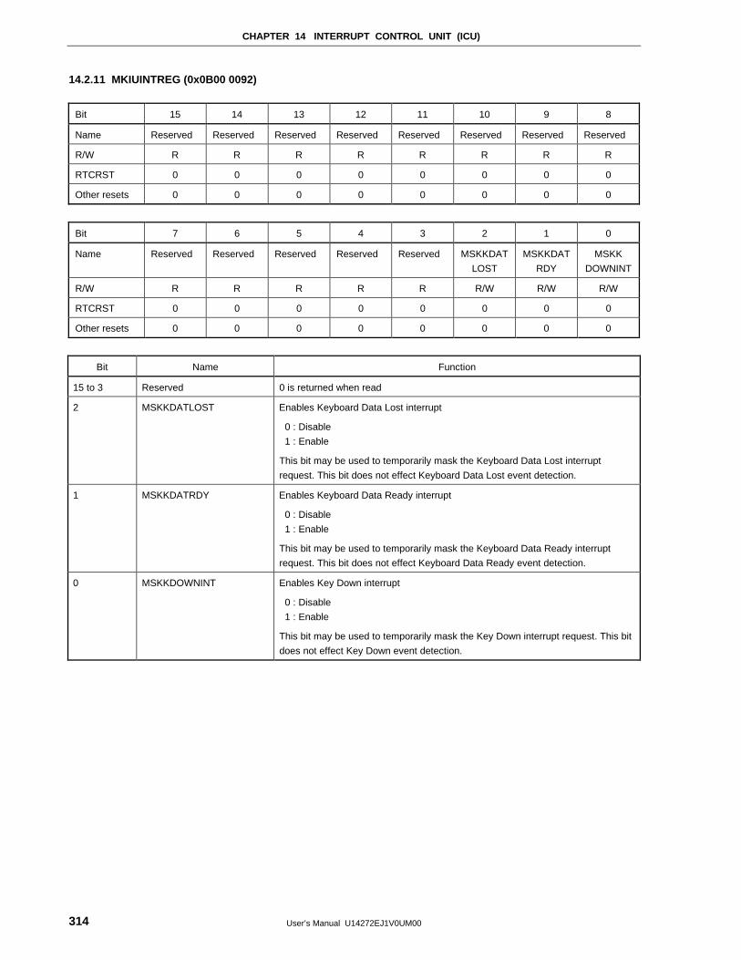
CHAPTER 14 INTERRUPT CONTROL UNIT (ICU)
User’s Manual U14272EJ1V0UM00314
14.2.11 MKIUINTREG (0x0B00 0092)
Bit 15 14 13 12 11 10 9 8
Name Reserved Reserved Reserved Reserved Reserved Reserved Reserved Reserved
R/W R R R R R R R R
RTCRST 0 0 0 0 0 0 0 0
Other resets 0 0 0 0 0 0 0 0
Bit 7 6 5 4 3 2 1 0
Name Reserved Reserved Reserved Reserved Reserved MSKKDAT
LOST
MSKKDAT
RDY
MSKK
DOWNINT
R/W R R R R R R/W R/W R/W
RTCRST 0 0 0 0 0 0 0 0
Other resets 0 0 0 0 0 0 0 0
Bit Name Function
15 to 3 Reserved 0 is returned when read
2 MSKKDATLOST Enables Keyboard Data Lost interrupt
0 : Disable
1 : Enable
This bit may be used to temporarily mask the Keyboard Data Lost interrupt
request. This bit does not effect Keyboard Data Lost event detection.
1 MSKKDATRDY Enables Keyboard Data Ready interrupt
0 : Disable
1 : Enable
This bit may be used to temporarily mask the Keyboard Data Ready interrupt
request. This bit does not effect Keyboard Data Ready event detection.
0 MSKKDOWNINT Enables Key Down interrupt
0 : Disable
1 : Enable
This bit may be used to temporarily mask the Key Down interrupt request. This bit
does not effect Key Down event detection.
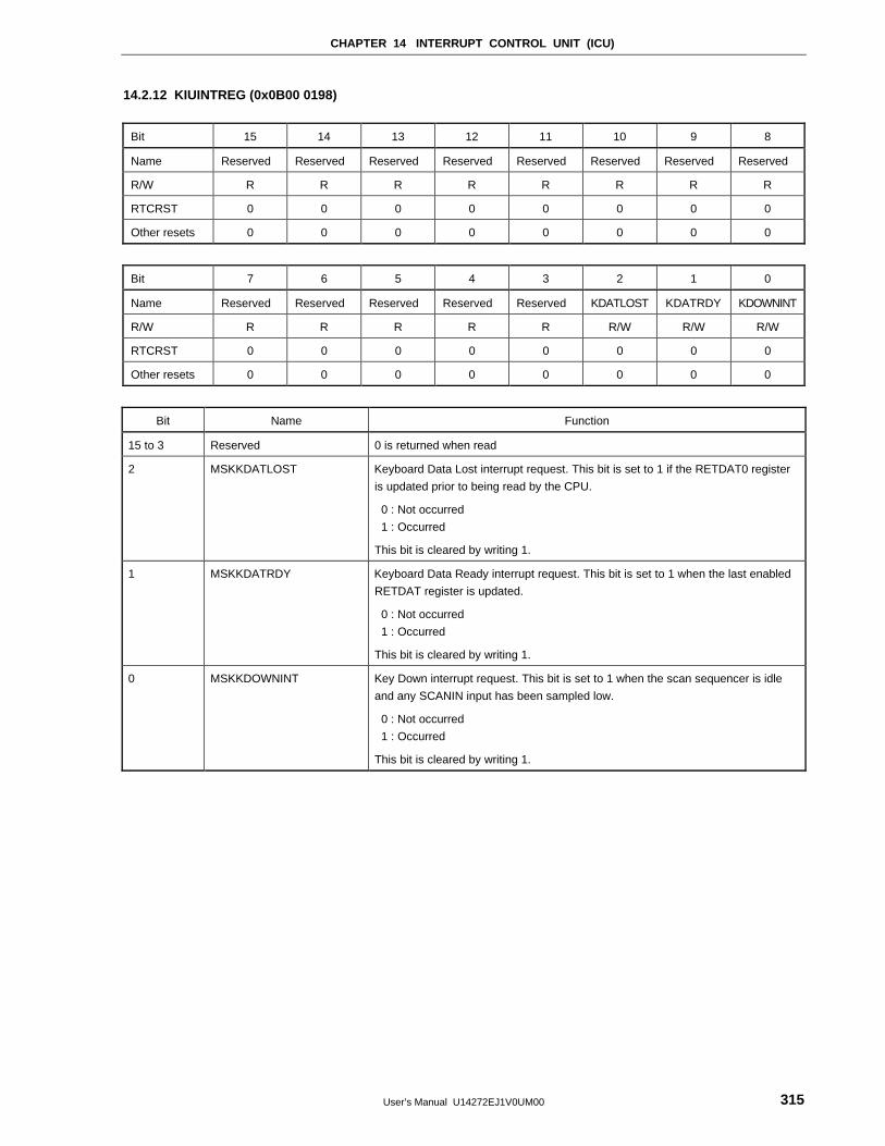
CHAPTER 14 INTERRUPT CONTROL UNIT (ICU)
User’s Manual U14272EJ1V0UM00 315
14.2.12 KIUINTREG (0x0B00 0198)
Bit 15 14 13 12 11 10 9 8
Name Reserved Reserved Reserved Reserved Reserved Reserved Reserved Reserved
R/W R R R R R R R R
RTCRST 0 0 0 0 0 0 0 0
Other resets 0 0 0 0 0 0 0 0
Bit 7 6 5 4 3 2 1 0
Name Reserved Reserved Reserved Reserved Reserved KDATLOST KDATRDY KDOWNINT
R/W R R R R R R/W R/W R/W
RTCRST 0 0 0 0 0 0 0 0
Other resets 0 0 0 0 0 0 0 0
Bit Name Function
15 to 3 Reserved 0 is returned when read
2 MSKKDATLOST Keyboard Data Lost interrupt request. This bit is set to 1 if the RETDAT0 register
is updated prior to being read by the CPU.
0 : Not occurred
1 : Occurred
This bit is cleared by writing 1.
1 MSKKDATRDY Keyboard Data Ready interrupt request. This bit is set to 1 when the last enabled
RETDAT register is updated.
0 : Not occurred
1 : Occurred
This bit is cleared by writing 1.
0 MSKKDOWNINT Key Down interrupt request. This bit is set to 1 when the scan sequencer is idle
and any SCANIN input has been sampled low.
0 : Not occurred
1 : Occurred
This bit is cleared by writing 1.

User’s Manual U14272EJ1V0UM00316
[MEMO]
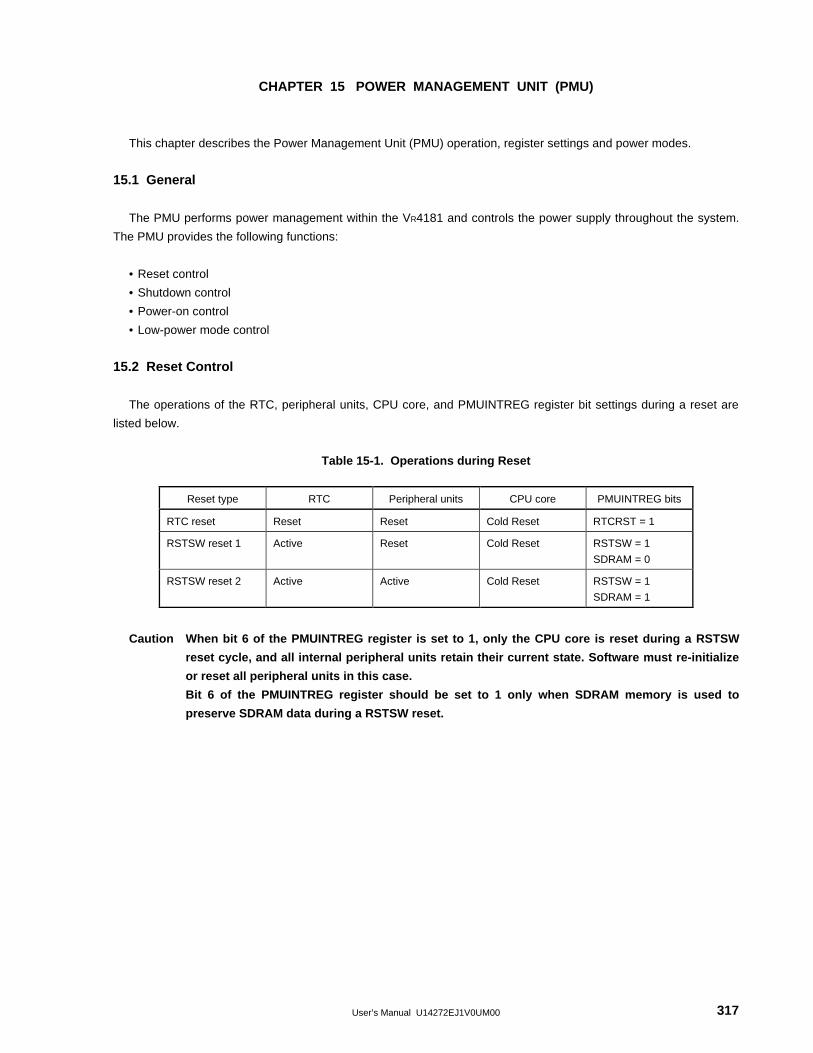
User’s Manual U14272EJ1V0UM00 317
CHAPTER 15 POWER MANAGEMENT UNIT (PMU)
This chapter describes the Power Management Unit (PMU) operation, register settings and power modes.
15.1 General
The PMU performs power management within the VR4181 and controls the power supply throughout the system.
The PMU provides the following functions:
• Reset control
• Shutdown control
• Power-on control
• Low-power mode control
15.2 Reset Control
The operations of the RTC, peripheral units, CPU core, and PMUINTREG register bit settings during a reset are
listed below.
Table 15-1. Operations during Reset
Reset type RTC Peripheral units CPU core PMUINTREG bits
RTC reset Reset Reset Cold Reset RTCRST = 1
RSTSW reset 1 Active Reset Cold Reset RSTSW = 1
SDRAM = 0
RSTSW reset 2 Active Active Cold Reset RSTSW = 1
SDRAM = 1
Caution When bit 6 of the PMUINTREG register is set to 1, only the CPU core is reset during a RSTSW
reset cycle, and all internal peripheral units retain their current state. Software must re-initialize
or reset all peripheral units in this case.
Bit 6 of the PMUINTREG register should be set to 1 only when SDRAM memory is used to
preserve SDRAM data during a RSTSW reset.
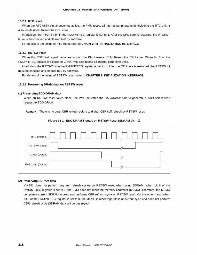
CHAPTER 15 POWER MANAGEMENT UNIT (PMU)
User’s Manual U14272EJ1V0UM00318
15.2.1 RTC reset
When the RTCRST# signal becomes active, the PMU resets all internal peripheral units including the RTC unit. It
also resets (Cold Reset) the CPU core.
In addition, the RTCRST bit in the PMUINTREG register is set to 1. After the CPU core is restarted, the RTCRST
bit must be checked and cleared to 0 by software.
For details of the timing of RTC reset, refer to CHAPTER 8 INITIALIZATION INTERFACE .
15.2.2 RSTSW reset
When the RSTSW# signal becomes active, the PMU resets (Cold Reset) the CPU core. When bit 6 of the
PMUINTREG register is cleared to 0, the PMU also resets all internal peripheral units.
In addition, the RSTSW bit in the PMUINTREG register is set to 1. After the CPU core is restarted, the RSTSW bit
must be checked and cleared to 0 by software.
For details of the timing of RSTSW reset, refer to CHAPTER 8 INITIALIZATION INTERFACE .
15.2.3 Preserving DRAM data on RSTSW reset
(1) Preserving EDO-DRAM data
When an RSTSW reset takes place, the PMU activates the CAS#/RAS# pins to generate a CBR self refresh
request to EDO DRAM.
Remark There is no burst CBR refresh before and after CBR self refresh by RSTSW reset.
Figure 15-1. EDO DRAM Signals on RSTSW Reset (SDRAM bit = 0)
RAS(1:0)# (Output)
CAS# (Output)
RSTSW# (Input)
RTC (Internal)
(2) Preserving SDRAM data
VR4181 does not perform any self refresh cycles on RSTSW reset when using SDRAM. When bit 6 of the
PMUINTREG register is set to 1, the PMU does not reset the memory controller (MEMC). Therefore, the MEMC
completes current SDRAM access and performs CBR refresh cycle on RSTSW reset. On the other hand, when
bit 6 of the PMUINTREG register is set to 0, the MEMC is reset regardless of current cycle and does not perform
CBR refresh cycle (SDRAM data will be destroyed).
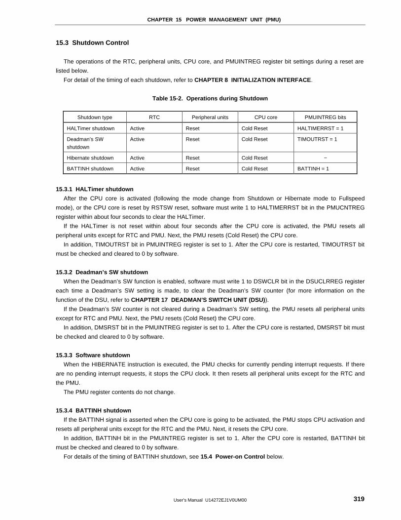
CHAPTER 15 POWER MANAGEMENT UNIT (PMU)
User’s Manual U14272EJ1V0UM00 319
15.3 Shutdown Control
The operations of the RTC, peripheral units, CPU core, and PMUINTREG register bit settings during a reset are
listed below.
For detail of the timing of each shutdown, refer to CHAPTER 8 INITIALIZATION INTERFACE .
Table 15-2. Operations during Shutdown
Shutdown type RTC Peripheral units CPU core PMUINTREG bits
HALTimer shutdown Active Reset Cold Reset HALTIMERRST = 1
Deadman’s SW
shutdown
Active Reset Cold Reset TIMOUTRST = 1
Hibernate shutdown Active Reset Cold Reset −
BATTINH shutdown Active Reset Cold Reset BATTINH = 1
15.3.1 HALTimer shutdown
After the CPU core is activated (following the mode change from Shutdown or Hibernate mode to Fullspeed
mode), or the CPU core is reset by RSTSW reset, software must write 1 to HALTIMERRST bit in the PMUCNTREG
register within about four seconds to clear the HALTimer.
If the HALTimer is not reset within about four seconds after the CPU core is activated, the PMU resets all
peripheral units except for RTC and PMU. Next, the PMU resets (Cold Reset) the CPU core.
In addition, TIMOUTRST bit in PMUINTREG register is set to 1. After the CPU core is restarted, TIMOUTRST bit
must be checked and cleared to 0 by software.
15.3.2 Deadman’s SW shutdown
When the Deadman’s SW function is enabled, software must write 1 to DSWCLR bit in the DSUCLRREG register
each time a Deadman’s SW setting is made, to clear the Deadman’s SW counter (for more information on the
function of the DSU, refer to CHAPTER 17 DEADMAN’S SWITCH UNIT (DSU) ).
If the Deadman’s SW counter is not cleared during a Deadman’s SW setting, the PMU resets all peripheral units
except for RTC and PMU. Next, the PMU resets (Cold Reset) the CPU core.
In addition, DMSRST bit in the PMUINTREG register is set to 1. After the CPU core is restarted, DMSRST bit must
be checked and cleared to 0 by software.
15.3.3 Software shutdown
When the HIBERNATE instruction is executed, the PMU checks for currently pending interrupt requests. If there
are no pending interrupt requests, it stops the CPU clock. It then resets all peripheral units except for the RTC and
the PMU.
The PMU register contents do not change.
15.3.4 BATTINH shutdown
If the BATTINH signal is asserted when the CPU core is going to be activated, the PMU stops CPU activation and
resets all peripheral units except for the RTC and the PMU. Next, it resets the CPU core.
In addition, BATTINH bit in the PMUINTREG register is set to 1. After the CPU core is restarted, BATTINH bit
must be checked and cleared to 0 by software.
For details of the timing of BATTINH shutdown, see 15.4 Power-on Control below.
CHAPTER 15 POWER MANAGEMENT UNIT (PMU)
User’s Manual U14272EJ1V0UM00320
15.4 Power-on Control
The causes of CPU core activation (mode change from shutdown mode or Hibernate mode to Fullspeed mode)
are called activation factors. There are twenty activation factors: a power switch interrupt (POWER), sixteen types of
GPIO activation interrupts (GPIO(15:0)), a DCD interrupt (DCD#), a CompactFlash interrupt, and an elapsed timer
interrupt.
Battery low detection (BATTINH/BATTINT# pin check) is a factor that prevents CPU core activation.
The period (power-on wait time), in which the POWERON pin is active at power-on, can be specified by using
PMUWAITREG register. After RTCRST, by which the CPU core is initialized, the period is 343.75 ms. Power-on wait
time can be specified when activation is caused by sources other than RTCRST.
When MPOWER signal is low level (Hibernate mode or during CPU core activation), to stop supplying voltage to
the 2.5 V power-supply systems is recommended to reduce the leak current. This means that this power supply can
become 0 V while the MPOWER signal is inactive. The following operation will not be affected by supplying voltage of
2.3 V or more to this power supply within the period from when the MPOWER signal becomes active to when PLL
starts oscillation.
Caution When the CPU core moves to the Hibernate mode by executing the HIBERNATE instruction, if an
activation factor occurs simultaneously, the CPU core may be activated without asserting the
POWERON signal after the MPOWER signal is once de-asserted. Moreover, if RSTSW#, which is
not an activation factor of the Hibernate mode, is asserted at the same time as the activation
factor occurs, the CPU core may be activated without asserting the POWERON signal after the
MPOWER signal is de-asserted once.
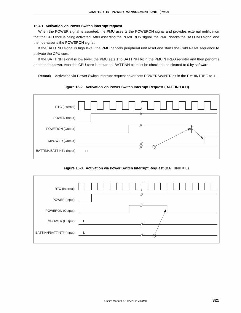
CHAPTER 15 POWER MANAGEMENT UNIT (PMU)
User’s Manual U14272EJ1V0UM00 321
15.4.1 Activation via Power Switch interrupt request
When the POWER signal is asserted, the PMU asserts the POWERON signal and provides external notification
that the CPU core is being activated. After asserting the POWERON signal, the PMU checks the BATTINH signal and
then de-asserts the POWERON signal.
If the BATTINH signal is high level, the PMU cancels peripheral unit reset and starts the Cold Reset sequence to
activate the CPU core.
If the BATTINH signal is low level, the PMU sets 1 to BATTINH bit in the PMUINTREG register and then performs
another shutdown. After the CPU core is restarted, BATTINH bit must be checked and cleared to 0 by software.
Remark Activation via Power Switch interrupt request never sets POWERSWINTR bit in the PMUINTREG to 1.
Figure 15-2. Activation via Power Switch Interrupt Request (BATTINH = H)
BATTINH/BATTINT# (Input)
MPOWER (Output)
POWERON (Output)
POWER (Input)
RTC (Internal)
H
Figure 15-3. Activation via Power Switch Interrupt Request (BATTINH = L)
BATTINH/BATTINT# (Input)
MPOWER (Output)
L
L
POWERON (Output)
POWER (Input)
RTC (Internal)
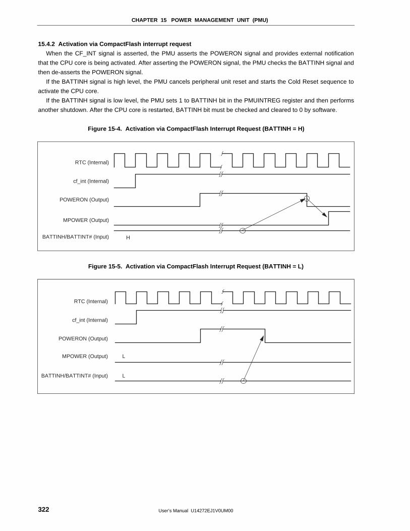
CHAPTER 15 POWER MANAGEMENT UNIT (PMU)
User’s Manual U14272EJ1V0UM00322
15.4.2 Activation via CompactFlash interrupt request
When the CF_INT signal is asserted, the PMU asserts the POWERON signal and provides external notification
that the CPU core is being activated. After asserting the POWERON signal, the PMU checks the BATTINH signal and
then de-asserts the POWERON signal.
If the BATTINH signal is high level, the PMU cancels peripheral unit reset and starts the Cold Reset sequence to
activate the CPU core.
If the BATTINH signal is low level, the PMU sets 1 to BATTINH bit in the PMUINTREG register and then performs
another shutdown. After the CPU core is restarted, BATTINH bit must be checked and cleared to 0 by software.
Figure 15-4. Activation via CompactFlash Interrupt Request (BATTINH = H)
BATTINH/BATTINT# (Input)
MPOWER (Output)
POWERON (Output)
cf_int (Internal)
RTC (Internal)
H
Figure 15-5. Activation via CompactFlash Interrupt Request (BATTINH = L)
BATTINH/BATTINT# (Input)
MPOWER (Output)
L
L
POWERON (Output)
cf_int (Internal)
RTC (Internal)
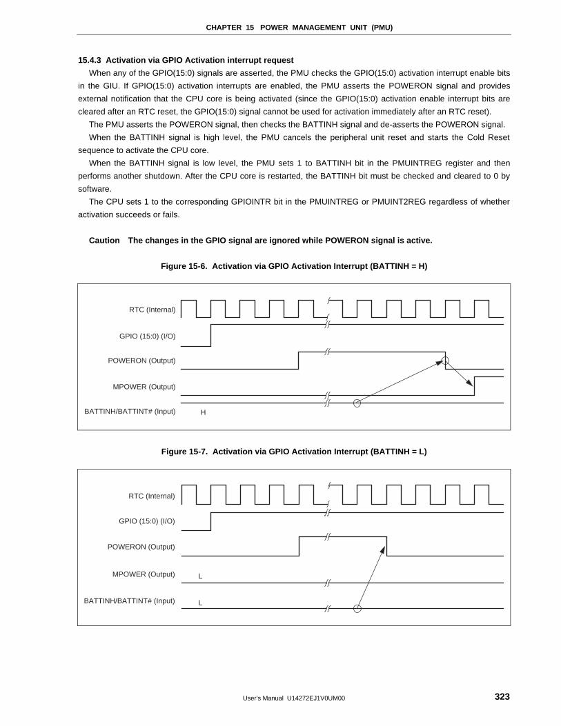
CHAPTER 15 POWER MANAGEMENT UNIT (PMU)
User’s Manual U14272EJ1V0UM00 323
15.4.3 Activation via GPIO Activation interrupt request
When any of the GPIO(15:0) signals are asserted, the PMU checks the GPIO(15:0) activation interrupt enable bits
in the GIU. If GPIO(15:0) activation interrupts are enabled, the PMU asserts the POWERON signal and provides
external notification that the CPU core is being activated (since the GPIO(15:0) activation enable interrupt bits are
cleared after an RTC reset, the GPIO(15:0) signal cannot be used for activation immediately after an RTC reset).
The PMU asserts the POWERON signal, then checks the BATTINH signal and de-asserts the POWERON signal.
When the BATTINH signal is high level, the PMU cancels the peripheral unit reset and starts the Cold Reset
sequence to activate the CPU core.
When the BATTINH signal is low level, the PMU sets 1 to BATTINH bit in the PMUINTREG register and then
performs another shutdown. After the CPU core is restarted, the BATTINH bit must be checked and cleared to 0 by
software.
The CPU sets 1 to the corresponding GPIOINTR bit in the PMUINTREG or PMUINT2REG regardless of whether
activation succeeds or fails.
Caution The changes in the GPIO signal are ignored while POWERON signal is active.
Figure 15-6. Activation via GPIO Activation Interrupt (BATTINH = H)
BATTINH/BATTINT# (Input)
MPOWER (Output)
POWERON (Output)
GPIO (15:0) (I/O)
RTC (Internal)
H
Figure 15-7. Activation via GPIO Activation Interrupt (BATTINH = L)
BATTINH/BATTINT# (Input)
MPOWER (Output)
POWERON (Output)
GPIO (15:0) (I/O)
RTC (Internal)
L
L
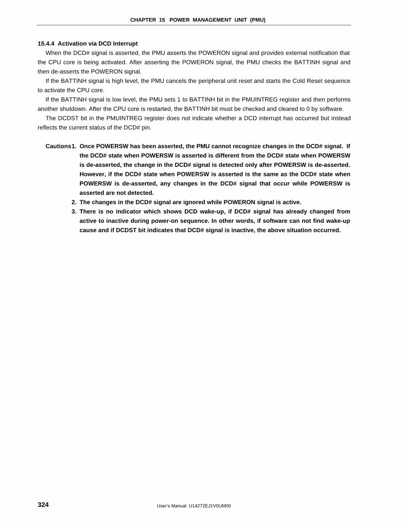
CHAPTER 15 POWER MANAGEMENT UNIT (PMU)
User’s Manual U14272EJ1V0UM00324
15.4.4 Activation via DCD Interrupt
When the DCD# signal is asserted, the PMU asserts the POWERON signal and provides external notification that
the CPU core is being activated. After asserting the POWERON signal, the PMU checks the BATTINH signal and
then de-asserts the POWERON signal.
If the BATTINH signal is high level, the PMU cancels the peripheral unit reset and starts the Cold Reset sequence
to activate the CPU core.
If the BATTINH signal is low level, the PMU sets 1 to BATTINH bit in the PMUINTREG register and then performs
another shutdown. After the CPU core is restarted, the BATTINH bit must be checked and cleared to 0 by software.
The DCDST bit in the PMUINTREG register does not indicate whether a DCD interrupt has occurred but instead
reflects the current status of the DCD# pin.
Cautions1. Once POWERSW has been asserted, the PMU cannot recognize changes in the DCD# signal. If
the DCD# state when POWERSW is asserted is different from the DCD# state when POWERSW
is de-asserted, the change in the DCD# signal is detected only after POWERSW is de-asserted.
However, if the DCD# state when POWERSW is asserted is the same as the DCD# state when
POWERSW is de-asserted, any changes in the DCD# signal that occur while POWERSW is
asserted are not detected.
2. The changes in the DCD# signal are ignored while POWERON signal is active.
3. There is no indicator which shows DCD wake-up, if DCD# signal has already changed from
active to inactive during power-on sequence. In other words, if software can not find wake-up
cause and if DCDST bit indicates that DCD# signal is inactive, the above situation occurred.
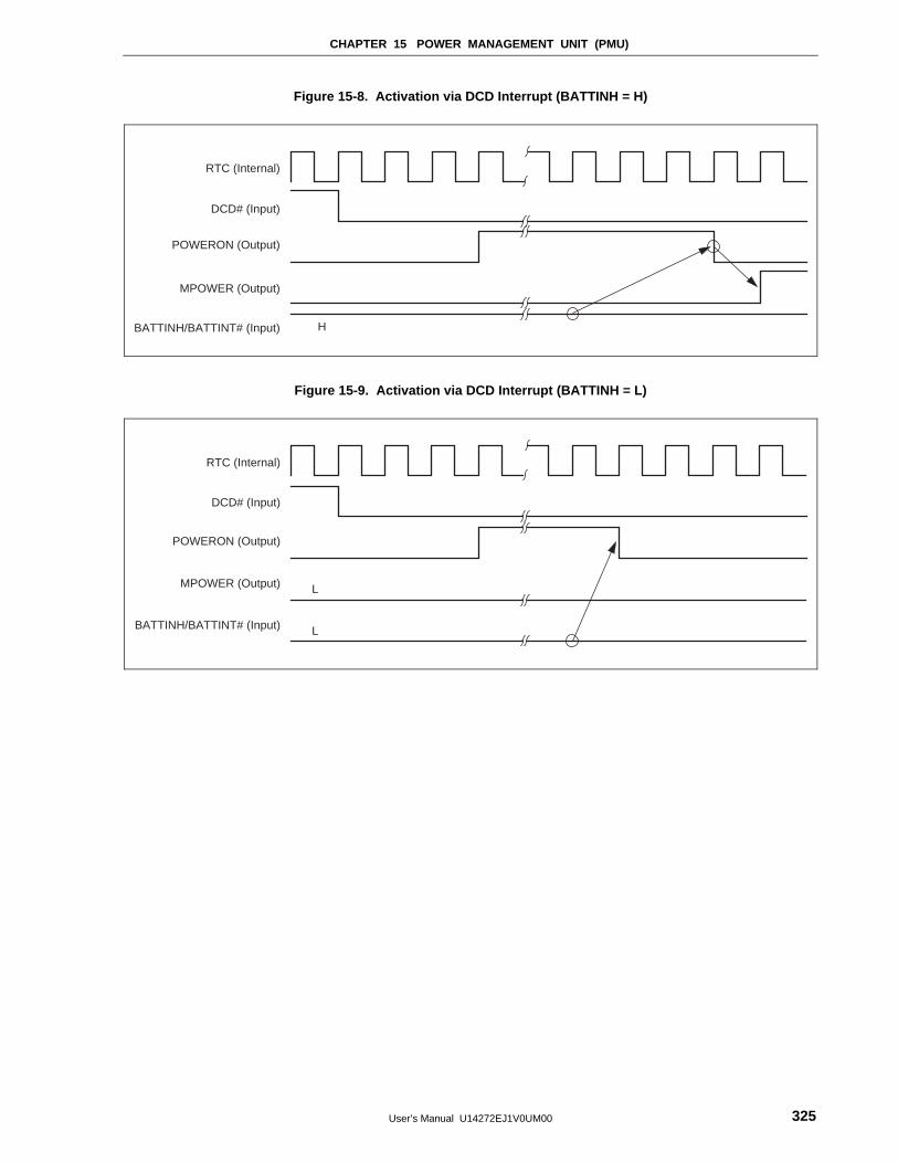
CHAPTER 15 POWER MANAGEMENT UNIT (PMU)
User’s Manual U14272EJ1V0UM00 325
Figure 15-8. Activation via DCD Interrupt (BATTINH = H)
BATTINH/BATTINT# (Input)
MPOWER (Output)
POWERON (Output)
DCD# (Input)
RTC (Internal)
H
Figure 15-9. Activation via DCD Interrupt (BATTINH = L)
BATTINH/BATTINT# (Input)
MPOWER (Output)
L
L
POWERON (Output)
DCD# (Input)
RTC (Internal)
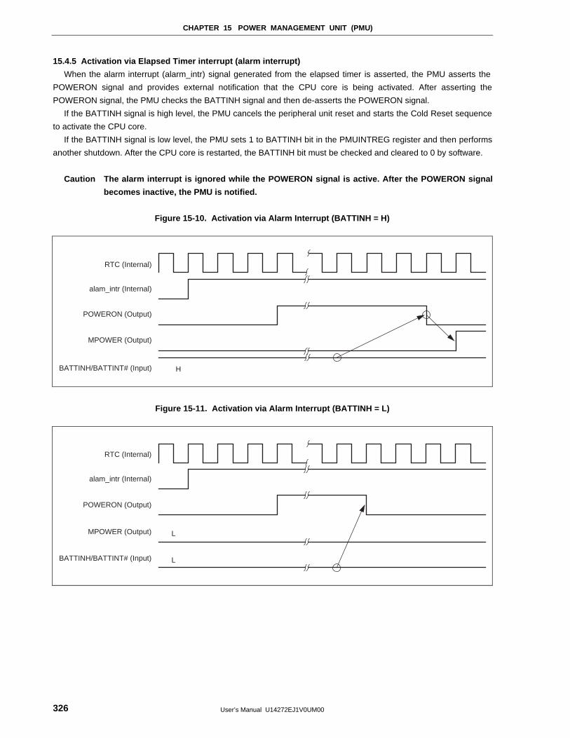
CHAPTER 15 POWER MANAGEMENT UNIT (PMU)
User’s Manual U14272EJ1V0UM00326
15.4.5 Activation via Elapsed Timer interrupt (alarm interrupt)
When the alarm interrupt (alarm_intr) signal generated from the elapsed timer is asserted, the PMU asserts the
POWERON signal and provides external notification that the CPU core is being activated. After asserting the
POWERON signal, the PMU checks the BATTINH signal and then de-asserts the POWERON signal.
If the BATTINH signal is high level, the PMU cancels the peripheral unit reset and starts the Cold Reset sequence
to activate the CPU core.
If the BATTINH signal is low level, the PMU sets 1 to BATTINH bit in the PMUINTREG register and then performs
another shutdown. After the CPU core is restarted, the BATTINH bit must be checked and cleared to 0 by software.
Caution The alarm interrupt is ignored while the POWERON signal is active. After the POWERON signal
becomes inactive, the PMU is notified.
Figure 15-10. Activation via Alarm Interrupt (BATTINH = H)
BATTINH/BATTINT# (Input)
MPOWER (Output)
POWERON (Output)
alam_intr (Internal)
RTC (Internal)
H
Figure 15-11. Activation via Alarm Interrupt (BATTINH = L)
BATTINH/BATTINT# (Input)
MPOWER (Output)
L
L
POWERON (Output)
alam_intr (Internal)
RTC (Internal)
CHAPTER 15 POWER MANAGEMENT UNIT (PMU)
User’s Manual U14272EJ1V0UM00 327
15.5 DRAM Interface Control
The PMU provides a register to control the DRAM interface during Hibernate mode. The DRAMHIBCTL register
permits software to directly control the state of the DRAM interface pins prior to executing a HIBERNATE instruction.
The DRAMHIBCTL register also provides status from the MEMC. The software flow when entering and exiting
Hibernate mode is shown below.
15.5.1 System request to enter Hibernate mode (EDO DRAM)
<1> Copy contents of all 2.5 V register Note that must be preserved during Hibernate mode into the battery
backed general purpose registers, MISCREG(0:15), in the GIU (i.e. DRAM type and configuration, ROM
type and configuration, etc.)
Note 3.3 V peripheral units (battery backed): PMU, GIU, LED, and RTC
2.5 V peripheral units: all peripheral except PMU, GIU, LED, and RTC
<2> Copy the codes for hibernation (<3> through <10> below) into the cache beginning at a 16-byte
boundary, and jump to the cached codes.
<3> Stop all peripheral clocks by writing zero to the CMUCLKMSK register.
<4> If DRAM cannot accept mixed use of burst and distributive CBR refresh, set refresh count to every 250
ns, and execute CBR refresh cycles during (0x3FFF × TClock period) + DRAM’s self refresh specification.
<5> Set refresh count to maximum in the BCURFCNTREG register to prevent a refresh cycle from interruption
of the hibernation sequence.
<6> Set SUSPEND bit in the DRAMHIBCTL register to 1 to request the MEMC to perform a burst refresh cycle
if enabled, and then put the DRAM into self refresh mode.
<7> Poll OK_STOP_CLK bit in the DRAMHIBCTL register to 1 to request the MEMC to perform a burst refresh
cycle and then put the DRAM into self refresh mode.
<8> Set DRAM_EN bit in the DRAMHIBCTL register to 1 so that the DRAM interface signals are latched and
held in a self refresh configuration (Now the VR4181 is ready to enter Hibernate mode).
<9> Set STOP_CLK bit in the DRAMHIBCTL register to 1 to request that TClock for MEMC stops.
<10> Execute a HIBERNATE instruction.
CHAPTER 15 POWER MANAGEMENT UNIT (PMU)
User’s Manual U14272EJ1V0UM00328
15.5.2 System request to enter Hibernate mode (SDRAM)
<1> Copy contents of all 2.5 V register Note that must be preserved during Hibernate mode into the battery
backed general purpose registers, MISCREG(0:15), in the GIU (i.e. DRAM type and configuration, ROM
type and configuration, etc.).
Note 3.3 V peripheral units (battery backed): PMU, GIU, LED, and RTC
2.5 V peripheral units: all peripheral except PMU, GIU, LED, and RTC
<2> Copy the codes for hibernation (<3> through <10> below) into the cache beginning at a 16-byte
boundary, and jump to the cached codes.
<3> Stop all peripheral clocks by writing zero to the CMUCLKMSK register.
<4> Set refresh count to maximum in the BCURFCNTREG register to prevent a refresh cycle from interruption
of the hibernation sequence.
<5> Set SUSPEND bit in the DRAMHIBCTL register to 1 to request the MEMC to perform a burst refresh cycle
and then put the DRAM into self refresh mode.
<6> Poll OK_STOP_CLK bit in the DRAMHIBCTL register to 1 to request the MEMC to perform a burst refresh
cycle and then put the DRAM into self refresh mode.
<7> Set DRAM_EN bit in the DRAMHIBCTL register to 1 so that the DRAM interface signals are latched and
held in a self-refresh configuration.
<8> Clear SUSPEND bit in the DRAMHIBCTL register to 0.
<9> Set STOP_CLK bit in the DRAMHIBCTL register to 1 to request that TClock stops.
<10> Execute a HIBERNATE instruction.
15.5.3 Wake-up from Hibernate mode (EDO DRAM)
<1> A wake-up event occurs such as a transition on the POWER pin, a DCD interrupt, etc. which causes the
PMU to start a power-on sequence.
<2> Power is applied to the external system of 3.3 V logic and the VR4181 of 2.5 V logic. The PMU waits until
the external 3.3 V and the 2.5 V power supply are stable, and then negates reset to the internal VR4110
CPU and VR4181 logic.
<3> Software execution resumes at the reset vector. At the same time, the MEMC begins a burst refresh cycle
if enabled, since SUSPEND bit in the DRAMHIBCTL register is still set to 1. Such refresh cycles are not
indicated on the DRAM interface pins since these pins are being driven with the latched self refresh
configuration when Hibernate mode was entered.
<4> Copy the codes for waking up (<5> through <13> below) into the cache beginning at a 16-byte boundary,
and jump to the cached codes.
<5> Software begins polling OK_STOP_CLK bit in the DRAMHIBCTL register to determine when the MEMC
has completed the burst refresh and entered self-refresh mode.
<6> Software should check and clear TIMOUTRST bit in the PMUINTREG register in the case a HALTimer
Shutdown had occurred.
<7> Reinitialize all the registers and peripherals during Hibernate mode and restore those registers saved in
the battery backed general purpose registers, MISKREG(0:15), in the GIU.
Remark Software must wait until the MEMC completes the burst refresh and enters self-refresh mode
before reinitializing the MEMC registers. Otherwise unpredictable behavior of MEMC could
result.
CHAPTER 15 POWER MANAGEMENT UNIT (PMU)
User’s Manual U14272EJ1V0UM00 329
<8> Clear DRAM_EN bit in the DRAMHIBCTL register to 0 so that the DRAM interface signals are again
driven directly by the MEMC.
<9> Clear SUSPEND bit to 0, which causes the MEMC to exit self-refresh mode and begin a burst refresh
cycle.
<10> Poll OK_USE_MEM bit to determine when the burst refresh cycle has completed.
<11> When OK_USE_MEM bit is set 1, the burst has completed.
<12> Set refresh count to every 250 ns, and execute CBR refresh cycles during (0x3FFF × TClock period) +
DRAM self refresh specification.
<13> Restore desired refresh rate to the BCURFCNTREG register, and then return to uncached segment.
<14> Software exits the wake-up sequence and returns control to the system.
15.5.4 Wake-up from Hibernate mode (SDRAM)
<1> A wake-up event occurs such as a transition on the POWER pin, a DCD interrupt, etc. which causes the
PMU to start a power-on sequence.
<2> Power is applied to the external system of 3.3 V logic and the VR4181 of 2.5 V logic. The PMU waits until
the external 3.3 V and the 2.5 V power supply are stable, and then negates reset to the internal VR4110
CPU and VR4181 logic.
<3> Software execution resumes at the reset vector.
<4> Software should check and clear TIMOUTRST bit in the PMUINTREG in the case that a HALTimer
Shutdown had occurred.
<5> Copy codes for waking up (<6> through <10> below) into the cache beginning at a 16-byte boundary, and
jump to the cached codes.
<6> Reinitialize all the registers and peripherals reset during Hibernate mode and restore those registers
saved in the battery backed general purpose registers, MISKREG(0:15), in the GIU.
<7> Clear DRAM_EN bit in the DRAMHIBCTL register to 0 so that the DRAM interface signals are again
driven directly by the MEMC.
<8> Set the BCURFCNTREG register to a value that will generate a refresh request every 1 µs.
<9> Wait until at least 0x3FFF × TClock period. This sequence is for burst refresh after self refresh.
<10> Restore desired refresh rate to the BCURFCNTREG register, and then return to uncached segment.
<11> Exit the wake-up sequence and return control to the system.
15.5.5 Suspend mode
In entering and exiting Suspend mode, skip the DRAM_EN bit in the DRAMHIBCTL register settings; otherwise,
the control of DRAMHIBCTL register is essentially the same as that of Hibernate mode.
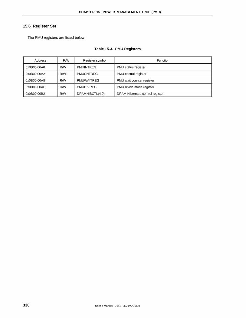
CHAPTER 15 POWER MANAGEMENT UNIT (PMU)
User’s Manual U14272EJ1V0UM00330
15.6 Register Set
The PMU registers are listed below:
Table 15-3. PMU Registers
Address R/W Register symbol Function
0x0B00 00A0 R/W PMUINTREG PMU status register
0x0B00 00A2 R/W PMUCNTREG PMU control register
0x0B00 00A8 R/W PMUWAITREG PMU wait counter register
0x0B00 00AC R/W PMUDIVREG PMU divide mode register
0x0B00 00B2 R/W DRAMHIBCTL(4:0) DRAM Hibernate control register
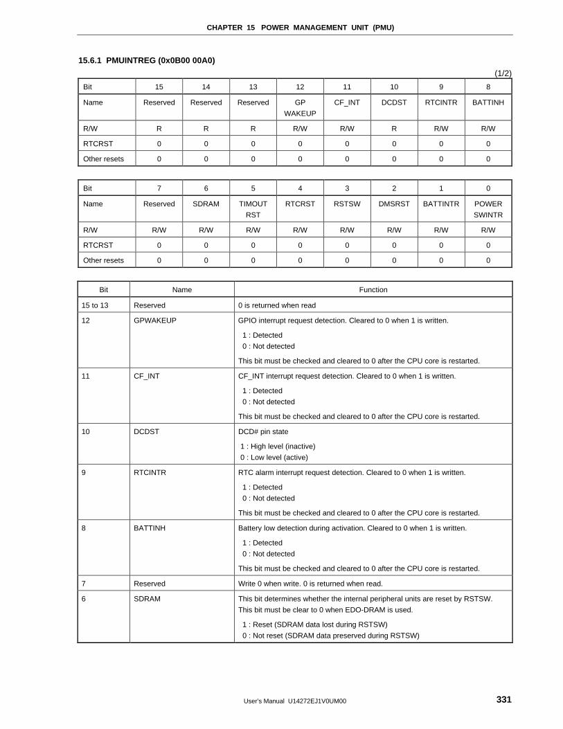
CHAPTER 15 POWER MANAGEMENT UNIT (PMU)
User’s Manual U14272EJ1V0UM00 331
15.6.1 PMUINTREG (0x0B00 00A0)
(1/2)
Bit 15 14 13 12 11 10 9 8
Name Reserved Reserved Reserved GP
WAKEUP
CF_INT DCDST RTCINTR BATTINH
R/W R R R R/W R/W R R/W R/W
RTCRST 0 0 0 0 0 0 0 0
Other resets 0 0 0 0 0 0 0 0
Bit 7 6 5 4 3 2 1 0
Name Reserved SDRAM TIMOUT
RST
RTCRST RSTSW DMSRST BATTINTR POWER
SWINTR
R/W R/W R/W R/W R/W R/W R/W R/W R/W
RTCRST 0 0 0 0 0 0 0 0
Other resets 0 0 0 0 0 0 0 0
Bit Name Function
15 to 13 Reserved 0 is returned when read
12 GPWAKEUP GPIO interrupt request detection. Cleared to 0 when 1 is written.
1 : Detected
0 : Not detected
This bit must be checked and cleared to 0 after the CPU core is restarted.
11 CF_INT CF_INT interrupt request detection. Cleared to 0 when 1 is written.
1 : Detected
0 : Not detected
This bit must be checked and cleared to 0 after the CPU core is restarted.
10 DCDST DCD# pin state
1 : High level (inactive)
0 : Low level (active)
9 RTCINTR RTC alarm interrupt request detection. Cleared to 0 when 1 is written.
1 : Detected
0 : Not detected
This bit must be checked and cleared to 0 after the CPU core is restarted.
8 BATTINH Battery low detection during activation. Cleared to 0 when 1 is written.
1 : Detected
0 : Not detected
This bit must be checked and cleared to 0 after the CPU core is restarted.
7 Reserved Write 0 when write. 0 is returned when read.
6 SDRAM This bit determines whether the internal peripheral units are reset by RSTSW.
This bit must be clear to 0 when EDO-DRAM is used.
1 : Reset (SDRAM data lost during RSTSW)
0 : Not reset (SDRAM data preserved during RSTSW)
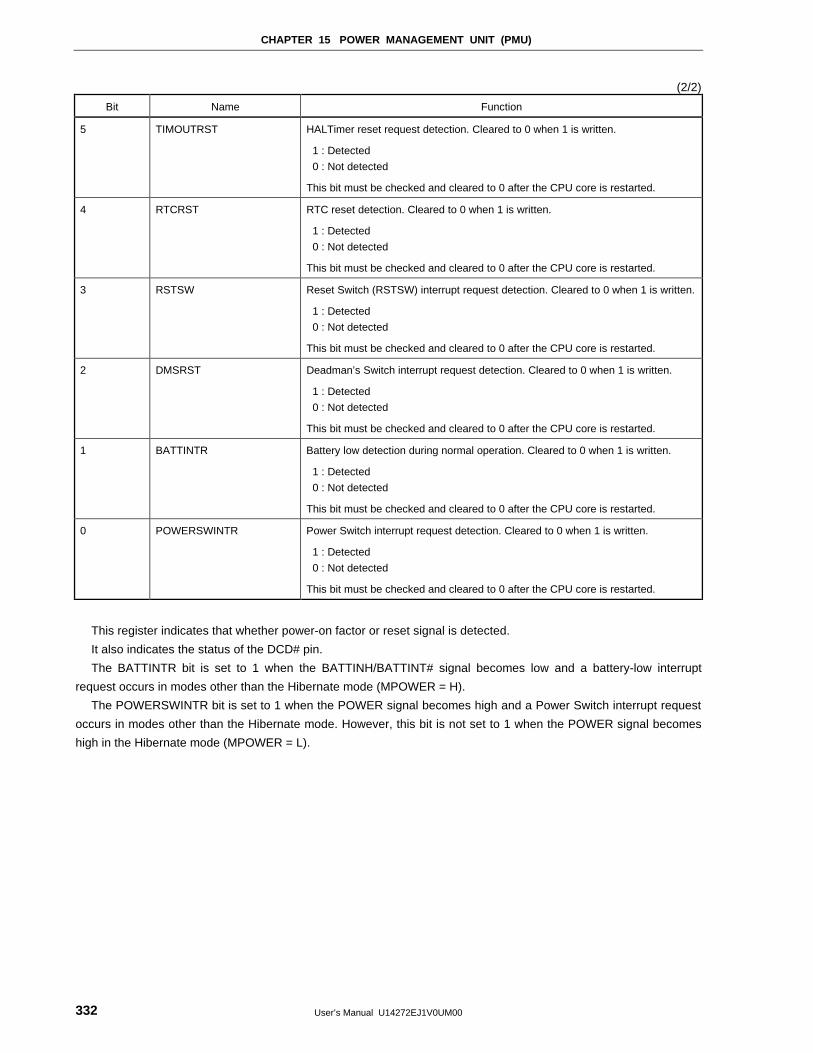
CHAPTER 15 POWER MANAGEMENT UNIT (PMU)
User’s Manual U14272EJ1V0UM00332
(2/2)
Bit Name Function
5 TIMOUTRST HALTimer reset request detection. Cleared to 0 when 1 is written.
1 : Detected
0 : Not detected
This bit must be checked and cleared to 0 after the CPU core is restarted.
4 RTCRST RTC reset detection. Cleared to 0 when 1 is written.
1 : Detected
0 : Not detected
This bit must be checked and cleared to 0 after the CPU core is restarted.
3 RSTSW Reset Switch (RSTSW) interrupt request detection. Cleared to 0 when 1 is written.
1 : Detected
0 : Not detected
This bit must be checked and cleared to 0 after the CPU core is restarted.
2 DMSRST Deadman’s Switch interrupt request detection. Cleared to 0 when 1 is written.
1 : Detected
0 : Not detected
This bit must be checked and cleared to 0 after the CPU core is restarted.
1 BATTINTR Battery low detection during normal operation. Cleared to 0 when 1 is written.
1 : Detected
0 : Not detected
This bit must be checked and cleared to 0 after the CPU core is restarted.
0 POWERSWINTR Power Switch interrupt request detection. Cleared to 0 when 1 is written.
1 : Detected
0 : Not detected
This bit must be checked and cleared to 0 after the CPU core is restarted.
This register indicates that whether power-on factor or reset signal is detected.
It also indicates the status of the DCD# pin.
The BATTINTR bit is set to 1 when the BATTINH/BATTINT# signal becomes low and a battery-low interrupt
request occurs in modes other than the Hibernate mode (MPOWER = H).
The POWERSWINTR bit is set to 1 when the POWER signal becomes high and a Power Switch interrupt request
occurs in modes other than the Hibernate mode. However, this bit is not set to 1 when the POWER signal becomes
high in the Hibernate mode (MPOWER = L).
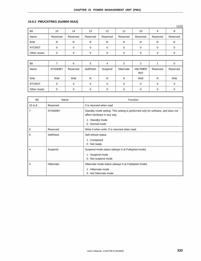
CHAPTER 15 POWER MANAGEMENT UNIT (PMU)
User’s Manual U14272EJ1V0UM00 333
15.6.2 PMUCNTREG (0x0B00 00A2)
(1/2)
Bit 15 14 13 12 11 10 9 8
Name Reserved Reserved Reserved Reserved Reserved Reserved Reserved Reserved
R/W R R R R R R R R
RTCRST 0 0 0 0 0 0 0 0
Other resets 0 0 0 0 0 0 0 0
Bit 7 6 5 4 3 2 1 0
Name STANDBY Reserved Selfrfresh Suspend Hibernate HALTIMER
RST
Reserved Reserved
R/W R/W R/W R R R R/W R R/W
RTCRST 0 0 0 0 0 0 0 0
Other resets 0 0 0 0 0 0 0 0
Bit Name Function
15 to 8 Reserved 0 is returned when read
7 STANDBY Standby mode setting. This setting is performed only for software, and does not
affect hardware in any way.
1 : Standby mode
0 : Normal mode
6 Reserved Write 0 when write. 0 is returned when read.
5 Selfrfresh Self refresh status
1 : Completed
0 : Not ready
4 Suspend Suspend mode status (always 0 at Fullspeed mode)
1 : Suspend mode
0 : Not suspend mode
3 Hibernate Hibernate mode status (always 0 at Fullspeed mode)
1 : Hibernate mode
0 : Not hibernate mode
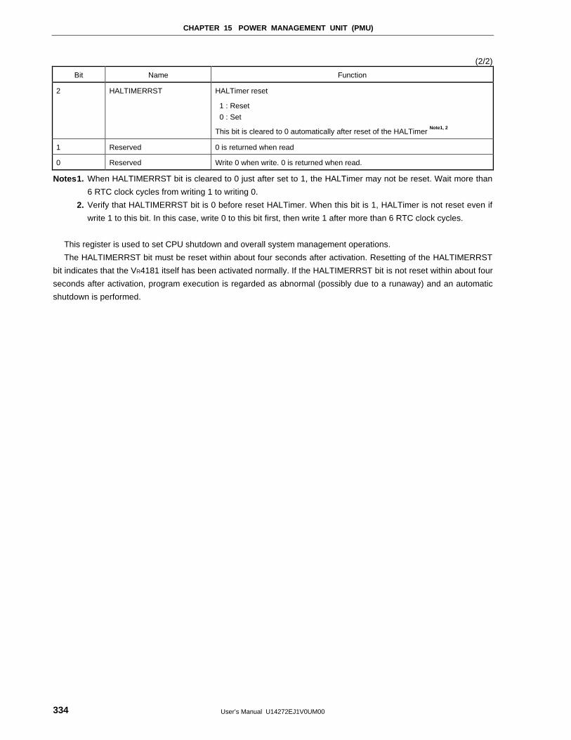
CHAPTER 15 POWER MANAGEMENT UNIT (PMU)
User’s Manual U14272EJ1V0UM00334
(2/2)
Bit Name Function
2 HALTIMERRST HALTimer reset
1 : Reset
0 : Set
This bit is cleared to 0 automatically after reset of the HALTimer Note1, 2
1 Reserved 0 is returned when read
0 Reserved Write 0 when write. 0 is returned when read.
Notes1. When HALTIMERRST bit is cleared to 0 just after set to 1, the HALTimer may not be reset. Wait more than
6 RTC clock cycles from writing 1 to writing 0.
2. Verify that HALTIMERRST bit is 0 before reset HALTimer. When this bit is 1, HALTimer is not reset even if
write 1 to this bit. In this case, write 0 to this bit first, then write 1 after more than 6 RTC clock cycles.
This register is used to set CPU shutdown and overall system management operations.
The HALTIMERRST bit must be reset within about four seconds after activation. Resetting of the HALTIMERRST
bit indicates that the VR4181 itself has been activated normally. If the HALTIMERRST bit is not reset within about four
seconds after activation, program execution is regarded as abnormal (possibly due to a runaway) and an automatic
shutdown is performed.
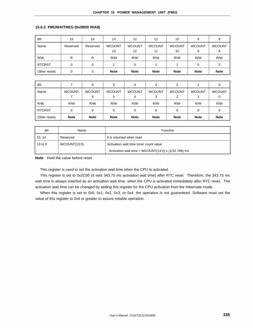
CHAPTER 15 POWER MANAGEMENT UNIT (PMU)
User’s Manual U14272EJ1V0UM00 335
15.6.3 PMUWAITREG (0x0B00 00A8)
Bit 15 14 13 12 11 10 9 8
Name Reserved Reserved WCOUNT
13
WCOUNT
12
WCOUNT
11
WCOUNT
10
WCOUNT
9
WCOUNT
8
R/W R R R/W R/W R/W R/W R/W R/W
RTCRST 0 0 1 0 1 1 0 0
Other resets 0 0 Note Note Note Note Note Note
Bit 7 6 5 4 3 2 1 0
Name WCOUNT
7
WCOUNT
6
WCOUNT
5
WCOUNT
4
WCOUNT
3
WCOUNT
2
WCOUNT
1
WCOUNT
0
R/W R/W R/W R/W R/W R/W R/W R/W R/W
RTCRST 0 0 0 0 0 0 0 0
Other resets Note Note Note Note Note Note Note Note
Bit Name Function
15, 14 Reserved 0 is returned when read
13 to 0 WCOUNT(13:0) Activation wait time timer count value
Activation wait time = WCOUNT(13:0) x (1/32.768) ms
Note Hold the value before reset
This register is used to set the activation wait time when the CPU is activated.
This register is set to 0x2C00 (it sets 343.75 ms activation wait time) after RTC reset. Therefore, the 343.75 ms
wait time is always inserted as an activation wait time, when the CPU is activated immediately after RTC reset. The
activation wait time can be changed by setting this register for the CPU activation from the Hibernate mode.
When this register is set to 0x0, 0x1, 0x2, 0x3, or 0x4, the operation is not guaranteed. Software must set the
value of this register to 0x4 or greater to assure reliable operation.
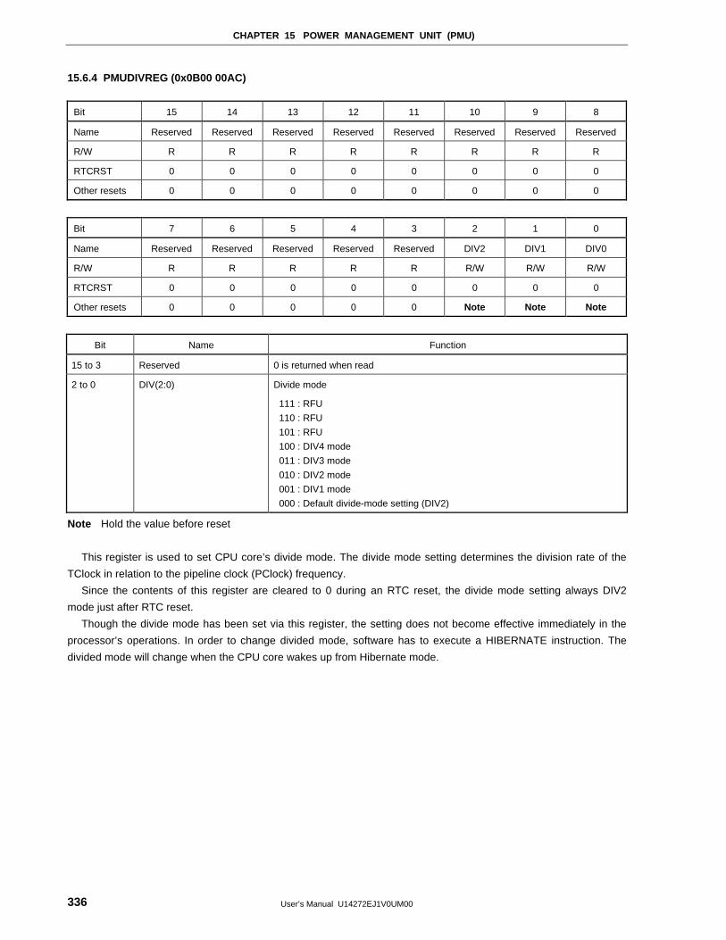
CHAPTER 15 POWER MANAGEMENT UNIT (PMU)
User’s Manual U14272EJ1V0UM00336
15.6.4 PMUDIVREG (0x0B00 00AC)
Bit 15 14 13 12 11 10 9 8
Name Reserved Reserved Reserved Reserved Reserved Reserved Reserved Reserved
R/W R R R R R R R R
RTCRST 0 0 0 0 0 0 0 0
Other resets 0 0 0 0 0 0 0 0
Bit 7 6 5 4 3 2 1 0
Name Reserved Reserved Reserved Reserved Reserved DIV2 DIV1 DIV0
R/W R R R R R R/W R/W R/W
RTCRST 0 0 0 0 0 0 0 0
Other resets 0 0 0 0 0 Note Note Note
Bit Name Function
15 to 3 Reserved 0 is returned when read
2 to 0 DIV(2:0) Divide mode
111 : RFU
110 : RFU
101 : RFU
100 : DIV4 mode
011 : DIV3 mode
010 : DIV2 mode
001 : DIV1 mode
000 : Default divide-mode setting (DIV2)
Note Hold the value before reset
This register is used to set CPU core’s divide mode. The divide mode setting determines the division rate of the
TClock in relation to the pipeline clock (PClock) frequency.
Since the contents of this register are cleared to 0 during an RTC reset, the divide mode setting always DIV2
mode just after RTC reset.
Though the divide mode has been set via this register, the setting does not become effective immediately in the
processor’s operations. In order to change divided mode, software has to execute a HIBERNATE instruction. The
divided mode will change when the CPU core wakes up from Hibernate mode.
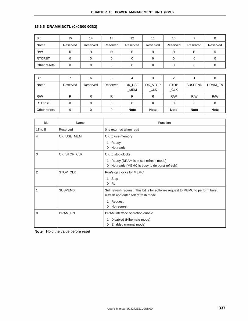
CHAPTER 15 POWER MANAGEMENT UNIT (PMU)
User’s Manual U14272EJ1V0UM00 337
15.6.5 DRAMHIBCTL (0x0B00 00B2)
Bit 15 14 13 12 11 10 9 8
Name Reserved Reserved Reserved Reserved Reserved Reserved Reserved Reserved
R/W R R R R R R R R
RTCRST 0 0 0 0 0 0 0 0
Other resets 0 0 0 0 0 0 0 0
Bit 7 6 5 4 3 2 1 0
Name Reserved Reserved Reserved OK_USE
_MEM
OK_STOP
_CLK
STOP
_CLK
SUSPEND DRAM_EN
R/W R R R R R R/W R/W R/W
RTCRST 0 0 0 0 0 0 0 0
Other resets 0 0 0 Note Note Note Note Note
Bit Name Function
15 to 5 Reserved 0 is returned when read
4 OK_USE_MEM OK to use memory
1 : Ready
0 : Not ready
3 OK_STOP_CLK OK to stop clocks
1 : Ready (DRAM is in self refresh mode)
0 : Not ready (MEMC is busy to do burst refresh)
2 STOP_CLK Run/stop clocks for MEMC
1 : Stop
0 : Run
1 SUSPEND Self refresh request. This bit is for software request to MEMC to perform burst
refresh and enter self refresh mode
1 : Request
0 : No request
0 DRAM_EN DRAM interface operation enable
1 : Disabled (Hibernate mode)
0 : Enabled (normal mode)
Note Hold the value before reset
CHAPTER 15 POWER MANAGEMENT UNIT (PMU)
User’s Manual U14272EJ1V0UM00338
15.7 VR4181 Power Mode
This section describes the VR4181 power modes in detail. The VR4181 supports the following four power modes:
• Fullspeed mode
• Standby mode
• Suspend mode
• Hibernate mode
15.7.1 Power mode and state transition
The VR4181 transits from Fullspeed mode to Standby mode, Suspend mode, or Hibernate mode by executing a
STANBY, SUSPEND, or HIBERNATE instruction respectively. RTCRST is always valid in every mode, and initializes
(resets) units in the VR4181 including the RTC. However, the VR4181 does not restart by RTCRST.
The figure on the following page, Figure 15-12, is a conceptual diagram showing the interaction and control of the
four power modes of the VR4181.
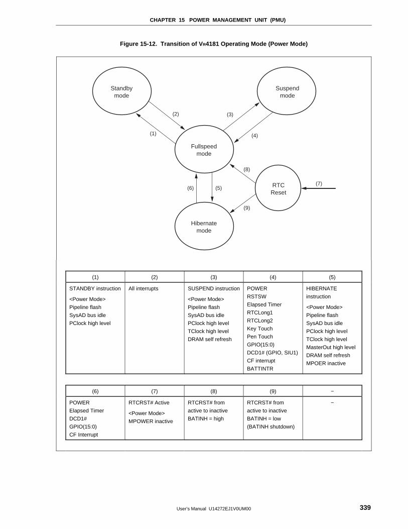
CHAPTER 15 POWER MANAGEMENT UNIT (PMU)
User’s Manual U14272EJ1V0UM00 339
Figure 15-12. Transition of V R4181 Operating Mode (Power Mode)
Standbymode
Suspendmode
Fullspeedmode
Hibernatemode
(3)
(4)
(2)
(6) (5)
(1)
RTCReset
(8)
(9)
(7)
(1) (2) (3) (4) (5)
STANDBY instruction
<Power Mode>
Pipeline flash
SysAD bus idle
PClock high level
All interrupts SUSPEND instruction
<Power Mode>
Pipeline flash
SysAD bus idle
PClock high level
TClock high level
DRAM self refresh
POWER
RSTSW
Elapsed Timer
RTCLong1
RTCLong2
Key Touch
Pen Touch
GPIO(15:0)
DCD1# (GPIO, SIU1)
CF interrupt
BATTINTR
HIBERNATE
instruction
<Power Mode>
Pipeline flash
SysAD bus idle
PClock high level
TClock high level
MasterOut high level
DRAM self refresh
MPOER inactive
(6) (7) (8) (9) −
POWER
Elapsed Timer
DCD1#
GPIO(15:0)
CF Interrupt
RTCRST# Active
<Power Mode>
MPOWER inactive
RTCRST# from
active to inactive
BATINH = high
RTCRST# from
active to inactive
BATINH = low
(BATINH shutdown)
−
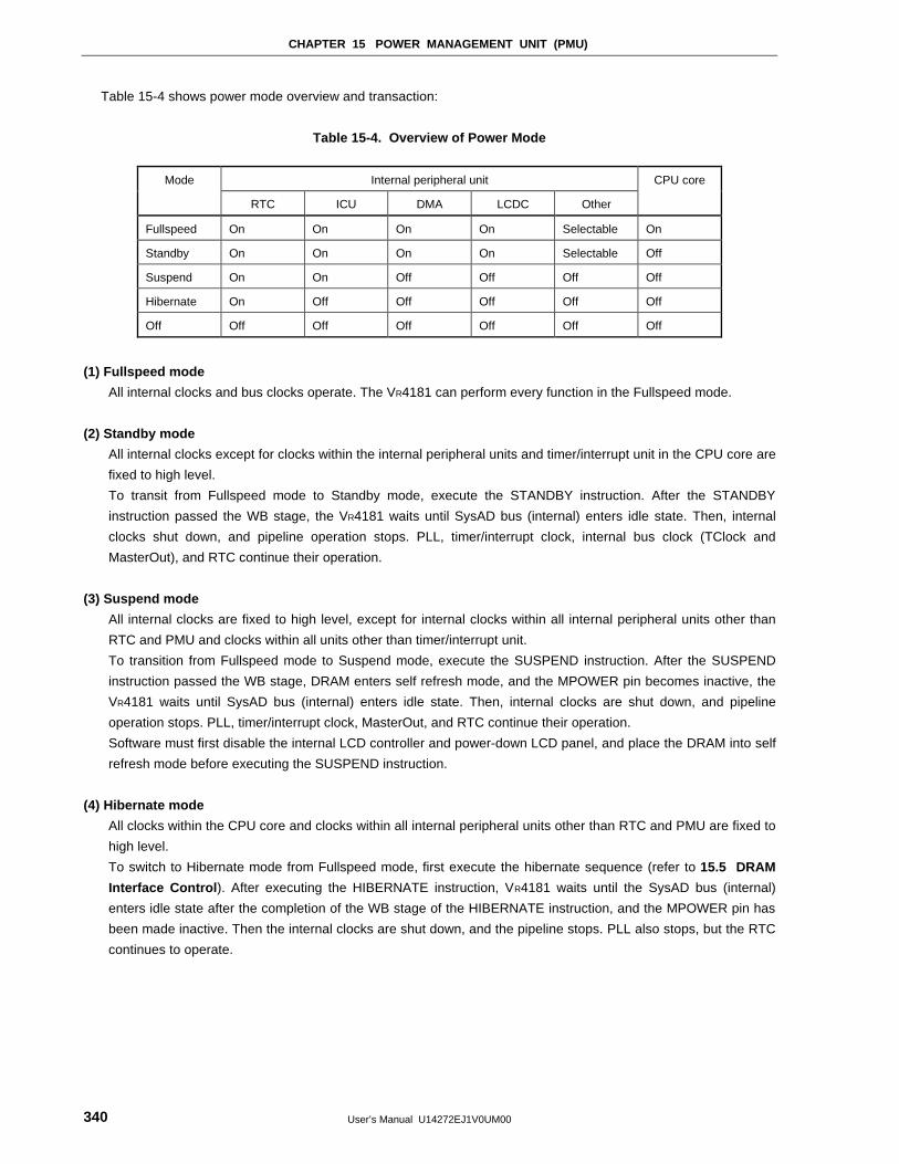
CHAPTER 15 POWER MANAGEMENT UNIT (PMU)
User’s Manual U14272EJ1V0UM00340
Table 15-4 shows power mode overview and transaction:
Table 15-4. Overview of Power Mode
Mode Internal peripheral unit CPU core
RTC ICU DMA LCDC Other
Fullspeed On On On On Selectable On
Standby On On On On Selectable Off
Suspend On On Off Off Off Off
Hibernate On Off Off Off Off Off
Off Off Off Off Off Off Off
(1) Fullspeed mode
All internal clocks and bus clocks operate. The VR4181 can perform every function in the Fullspeed mode.
(2) Standby mode
All internal clocks except for clocks within the internal peripheral units and timer/interrupt unit in the CPU core are
fixed to high level.
To transit from Fullspeed mode to Standby mode, execute the STANDBY instruction. After the STANDBY
instruction passed the WB stage, the VR4181 waits until SysAD bus (internal) enters idle state. Then, internal
clocks shut down, and pipeline operation stops. PLL, timer/interrupt clock, internal bus clock (TClock and
MasterOut), and RTC continue their operation.
(3) Suspend mode
All internal clocks are fixed to high level, except for internal clocks within all internal peripheral units other than
RTC and PMU and clocks within all units other than timer/interrupt unit.
To transition from Fullspeed mode to Suspend mode, execute the SUSPEND instruction. After the SUSPEND
instruction passed the WB stage, DRAM enters self refresh mode, and the MPOWER pin becomes inactive, the
VR4181 waits until SysAD bus (internal) enters idle state. Then, internal clocks are shut down, and pipeline
operation stops. PLL, timer/interrupt clock, MasterOut, and RTC continue their operation.
Software must first disable the internal LCD controller and power-down LCD panel, and place the DRAM into self
refresh mode before executing the SUSPEND instruction.
(4) Hibernate mode
All clocks within the CPU core and clocks within all internal peripheral units other than RTC and PMU are fixed to
high level.
To switch to Hibernate mode from Fullspeed mode, first execute the hibernate sequence (refer to 15.5 DRAM
Interface Control ). After executing the HIBERNATE instruction, VR4181 waits until the SysAD bus (internal)
enters idle state after the completion of the WB stage of the HIBERNATE instruction, and the MPOWER pin has
been made inactive. Then the internal clocks are shut down, and the pipeline stops. PLL also stops, but the RTC
continues to operate.
User’s Manual U14272EJ1V0UM00 341
CHAPTER 16 REALTIME CLOCK UNIT (RTC)
This chapter describes the RTC unit’s operations and register settings.
16.1 General
The RTC unit has a total of three timers, including the following two types.
• RTCLong...........This is a 24-bit programmable counter that counts down using 32.768 kHz frequency. Cycle
interrupts occur for up to 512 seconds. The RTC unit includes two RTCLong timers.
• ElapsedTime .....This is a 48-bit up counter that counts up using 32.768 kHz frequency. It counts up to 272
years before returning to zero. It includes 48-bit comparator (ECMPHREG, ECMPLREG, and
ECMPMREG) and 48-bit alarm time register (ETIMELREG, ETIMEMREG, and ETIMEHREG)
to enable interrupts to occur at specified times.
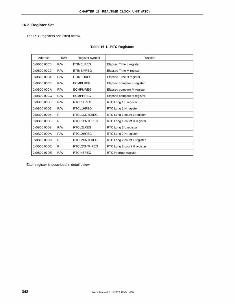
CHAPTER 16 REALTIME CLOCK UNIT (RTC)
User’s Manual U14272EJ1V0UM00342
16.2 Register Set
The RTC registers are listed below.
Table 16-1. RTC Registers
Address R/W Register symbol Function
0x0B00 00C0 R/W ETIMELREG Elapsed Time L register
0x0B00 00C2 R/W ETIMEMREG Elapsed Time M register
0x0B00 00C4 R/W ETIMEHREG Elapsed Time H register
0x0B00 00C8 R/W ECMPLREG Elapsed compare L register
0x0B00 00CA R/W ECMPMREG Elapsed compare M register
0x0B00 00CC R/W ECMPHREG Elapsed compare H register
0x0B00 00D0 R/W RTCL1LREG RTC Long 1 L register
0x0B00 00D2 R/W RTCL1HREG RTC Long 1 H register
0x0B00 00D4 R RTCL1CNTLREG RTC Long 1 count L register
0x0B00 00D6 R RTCL1CNTHREG RTC Long 1 count H register
0x0B00 00D8 R/W RTCL2LREG RTC Long 2 L register
0x0B00 00DA R/W RTCL2HREG RTC Long 2 H register
0x0B00 00DC R RTCL2CNTLREG RTC Long 2 count L register
0x0B00 00DE R RTCL2CNTHREG RTC Long 2 count H register
0x0B00 01DE R/W RTCINTREG RTC interrupt register
Each register is described in detail below.
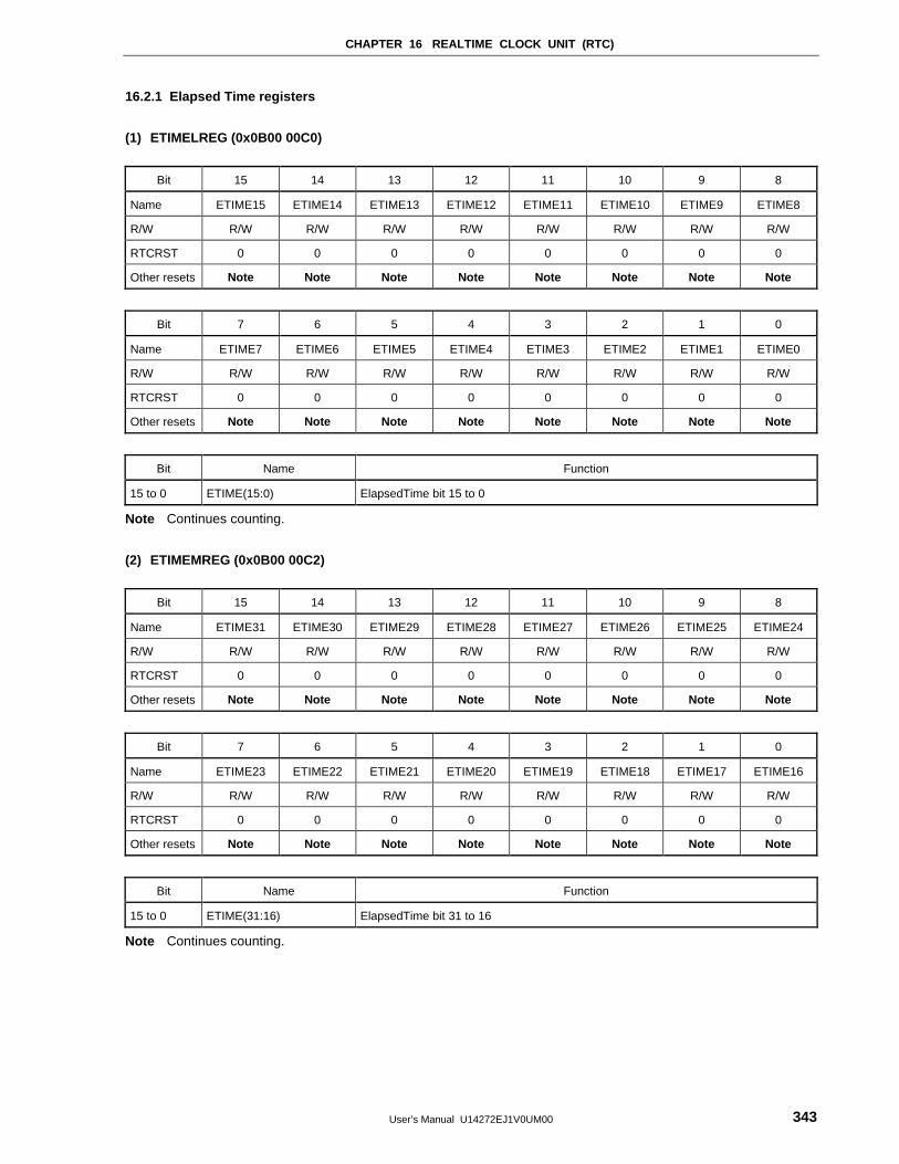
CHAPTER 16 REALTIME CLOCK UNIT (RTC)
User’s Manual U14272EJ1V0UM00 343
16.2.1 Elapsed Time registers
(1) ETIMELREG (0x0B00 00C0)
Bit 15 14 13 12 11 10 9 8
Name ETIME15 ETIME14 ETIME13 ETIME12 ETIME11 ETIME10 ETIME9 ETIME8
R/W R/W R/W R/W R/W R/W R/W R/W R/W
RTCRST 0 0 0 0 0 0 0 0
Other resets Note Note Note Note Note Note Note Note
Bit 7 6 5 4 3 2 1 0
Name ETIME7 ETIME6 ETIME5 ETIME4 ETIME3 ETIME2 ETIME1 ETIME0
R/W R/W R/W R/W R/W R/W R/W R/W R/W
RTCRST 0 0 0 0 0 0 0 0
Other resets Note Note Note Note Note Note Note Note
Bit Name Function
15 to 0 ETIME(15:0) ElapsedTime bit 15 to 0
Note Continues counting.
(2) ETIMEMREG (0x0B00 00C2)
Bit 15 14 13 12 11 10 9 8
Name ETIME31 ETIME30 ETIME29 ETIME28 ETIME27 ETIME26 ETIME25 ETIME24
R/W R/W R/W R/W R/W R/W R/W R/W R/W
RTCRST 0 0 0 0 0 0 0 0
Other resets Note Note Note Note Note Note Note Note
Bit 7 6 5 4 3 2 1 0
Name ETIME23 ETIME22 ETIME21 ETIME20 ETIME19 ETIME18 ETIME17 ETIME16
R/W R/W R/W R/W R/W R/W R/W R/W R/W
RTCRST 0 0 0 0 0 0 0 0
Other resets Note Note Note Note Note Note Note Note
Bit Name Function
15 to 0 ETIME(31:16) ElapsedTime bit 31 to 16
Note Continues counting.
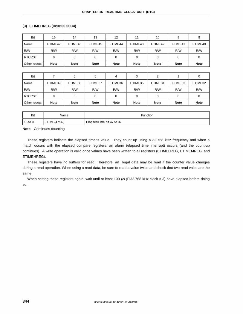
CHAPTER 16 REALTIME CLOCK UNIT (RTC)
User’s Manual U14272EJ1V0UM00344
(3) ETIMEHREG (0x0B00 00C4)
Bit 15 14 13 12 11 10 9 8
Name ETIME47 ETIME46 ETIME45 ETIME44 ETIME43 ETIME42 ETIME41 ETIME40
R/W R/W R/W R/W R/W R/W R/W R/W R/W
RTCRST 0 0 0 0 0 0 0 0
Other resets Note Note Note Note Note Note Note Note
Bit 7 6 5 4 3 2 1 0
Name ETIME39 ETIME38 ETIME37 ETIME36 ETIME35 ETIME34 ETIME33 ETIME32
R/W R/W R/W R/W R/W R/W R/W R/W R/W
RTCRST 0 0 0 0 0 0 0 0
Other resets Note Note Note Note Note Note Note Note
Bit Name Function
15 to 0 ETIME(47:32) ElapsedTime bit 47 to 32
Note Continues counting
These registers indicate the elapsed timer’s value. They count up using a 32.768 kHz frequency and when a
match occurs with the elapsed compare registers, an alarm (elapsed time interrupt) occurs (and the count-up
continues). A write operation is valid once values have been written to all registers (ETIMELREG, ETIMEMREG, and
ETIMEHREG).
These registers have no buffers for read. Therefore, an illegal data may be read if the counter value changes
during a read operation. When using a read data, be sure to read a value twice and check that two read vales are the
same.
When setting these registers again, wait until at least 100 µs (≅ 32.768 kHz clock × 3) have elapsed before doing
so.
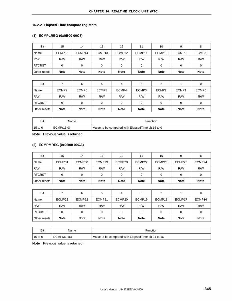
CHAPTER 16 REALTIME CLOCK UNIT (RTC)
User’s Manual U14272EJ1V0UM00 345
16.2.2 Elapsed Time compare registers
(1) ECMPLREG (0x0B00 00C8)
Bit 15 14 13 12 11 10 9 8
Name ECMP15 ECMP14 ECMP13 ECMP12 ECMP11 ECMP10 ECMP9 ECMP8
R/W R/W R/W R/W R/W R/W R/W R/W R/W
RTCRST 0 0 0 0 0 0 0 0
Other resets Note Note Note Note Note Note Note Note
Bit 7 6 5 4 3 2 1 0
Name ECMP7 ECMP6 ECMP5 ECMP4 ECMP3 ECMP2 ECMP1 ECMP0
R/W R/W R/W R/W R/W R/W R/W R/W R/W
RTCRST 0 0 0 0 0 0 0 0
Other resets Note Note Note Note Note Note Note Note
Bit Name Function
15 to 0 ECMP(15:0) Value to be compared with ElapsedTime bit 15 to 0
Note Previous value is retained.
(2) ECMPMREG (0x0B00 00CA)
Bit 15 14 13 12 11 10 9 8
Name ECMP31 ECMP30 ECMP29 ECMP28 ECMP27 ECMP26 ECMP25 ECMP24
R/W R/W R/W R/W R/W R/W R/W R/W R/W
RTCRST 0 0 0 0 0 0 0 0
Other resets Note Note Note Note Note Note Note Note
Bit 7 6 5 4 3 2 1 0
Name ECMP23 ECMP22 ECMP21 ECMP20 ECMP19 ECMP18 ECMP17 ECMP16
R/W R/W R/W R/W R/W R/W R/W R/W R/W
RTCRST 0 0 0 0 0 0 0 0
Other resets Note Note Note Note Note Note Note Note
Bit Name Function
15 to 0 ECMP(31:16) Value to be compared with ElapsedTime bit 31 to 16
Note Previous value is retained.
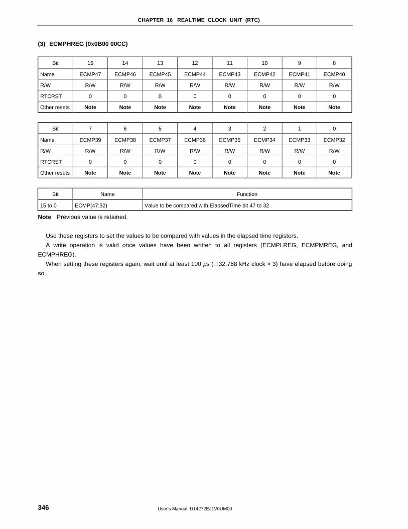
CHAPTER 16 REALTIME CLOCK UNIT (RTC)
User’s Manual U14272EJ1V0UM00346
(3) ECMPHREG (0x0B00 00CC)
Bit 15 14 13 12 11 10 9 8
Name ECMP47 ECMP46 ECMP45 ECMP44 ECMP43 ECMP42 ECMP41 ECMP40
R/W R/W R/W R/W R/W R/W R/W R/W R/W
RTCRST 0 0 0 0 0 0 0 0
Other resets Note Note Note Note Note Note Note Note
Bit 7 6 5 4 3 2 1 0
Name ECMP39 ECMP38 ECMP37 ECMP36 ECMP35 ECMP34 ECMP33 ECMP32
R/W R/W R/W R/W R/W R/W R/W R/W R/W
RTCRST 0 0 0 0 0 0 0 0
Other resets Note Note Note Note Note Note Note Note
Bit Name Function
15 to 0 ECMP(47:32) Value to be compared with ElapsedTime bit 47 to 32
Note Previous value is retained.
Use these registers to set the values to be compared with values in the elapsed time registers.
A write operation is valid once values have been written to all registers (ECMPLREG, ECMPMREG, and
ECMPHREG).
When setting these registers again, wait until at least 100 µs (≅ 32.768 kHz clock × 3) have elapsed before doing
so.
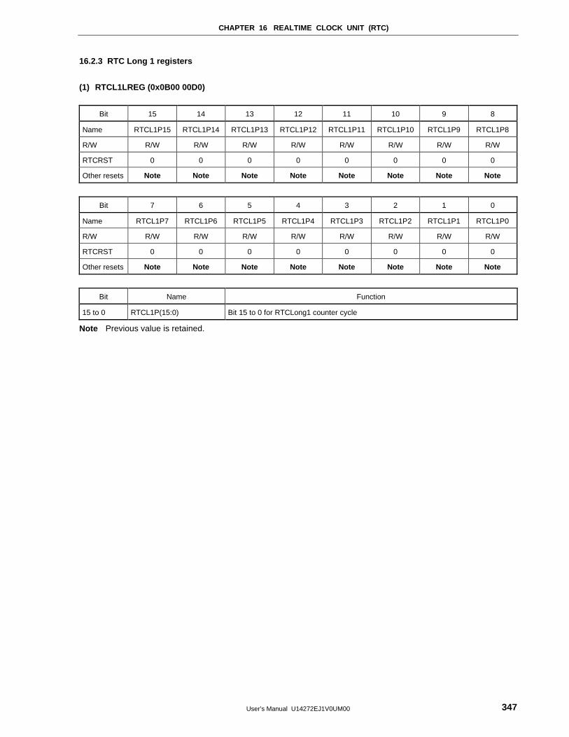
CHAPTER 16 REALTIME CLOCK UNIT (RTC)
User’s Manual U14272EJ1V0UM00 347
16.2.3 RTC Long 1 registers
(1) RTCL1LREG (0x0B00 00D0)
Bit 15 14 13 12 11 10 9 8
Name RTCL1P15 RTCL1P14 RTCL1P13 RTCL1P12 RTCL1P11 RTCL1P10 RTCL1P9 RTCL1P8
R/W R/W R/W R/W R/W R/W R/W R/W R/W
RTCRST 0 0 0 0 0 0 0 0
Other resets Note Note Note Note Note Note Note Note
Bit 7 6 5 4 3 2 1 0
Name RTCL1P7 RTCL1P6 RTCL1P5 RTCL1P4 RTCL1P3 RTCL1P2 RTCL1P1 RTCL1P0
R/W R/W R/W R/W R/W R/W R/W R/W R/W
RTCRST 0 0 0 0 0 0 0 0
Other resets Note Note Note Note Note Note Note Note
Bit Name Function
15 to 0 RTCL1P(15:0) Bit 15 to 0 for RTCLong1 counter cycle
Note Previous value is retained.

CHAPTER 16 REALTIME CLOCK UNIT (RTC)
User’s Manual U14272EJ1V0UM00348
(2) RTCL1HREG (0x0B00 00D2)
Bit 15 14 13 12 11 10 9 8
Name Reserved Reserved Reserved Reserved Reserved Reserved Reserved Reserved
R/W R R R R R R R R
RTCRST 0 0 0 0 0 0 0 0
Other resets Note Note Note Note Note Note Note Note
Bit 7 6 5 4 3 2 1 0
Name RTCL1P23 RTCL1P22 RTCL1P21 RTCL1P20 RTCL1P19 RTCL1P18 RTCL1P17 RTCL1P16
R/W R/W R/W R/W R/W R/W R/W R/W R/W
RTCRST 0 0 0 0 0 0 0 0
Other resets Note Note Note Note Note Note Note Note
Bit Name Function
15 to 8 Reserved 0 is returned when read
7 to 0 RTCL1P(23:16) Bit 23 to 16 for RTCLong1 counter cycle
Note Previous value is retained.
Use these registers to set the RTCLong1 counter cycle. The RTCLong1 counter begins its countdown at the
value written to these registers.
A write operation is valid once values have been written to both registers (RTCL1LREG and RTCL1HREG).
When setting these registers again, wait until at least 100 µs (≅ 32.768 kHz clock × 3) have elapsed before doing
so.
Cautions 1. The RTC unit is stopped when all zeros are written.
2. Any combined setting of “RTCL1HREG = 0x0000” and “RTCL1LREG = 0x0001, 0x0002,
0x0003, 0x0004” is prohibited.

CHAPTER 16 REALTIME CLOCK UNIT (RTC)
User’s Manual U14272EJ1V0UM00 349
16.2.4 RTC Long 1 Count registers
(1) RTCL1CNTLREG (0x0B00 00D4)
Bit 15 14 13 12 11 10 9 8
Name RTCL1C15 RTCL1C14 RTCL1C13 RTCL1C12 RTCL1C11 RTCL1C10 RTCL1C9 RTCL1C8
R/W R R R R R R R R
RTCRST 0 0 0 0 0 0 0 0
Other resets Note Note Note Note Note Note Note Note
Bit 7 6 5 4 3 2 1 0
Name RTCL1C7 RTCL1C6 RTCL1C5 RTCL1C4 RTCL1C3 RTCL1C2 RTCL1C1 RTCL1C0
R/W R R R R R R R R
RTCRST 0 0 0 0 0 0 0 0
Other resets Note Note Note Note Note Note Note Note
Bit Name Function
15 to 0 RTCL1C(15:0) RTCLong1 counter bit 15 to 0
Note Continues counting.

CHAPTER 16 REALTIME CLOCK UNIT (RTC)
User’s Manual U14272EJ1V0UM00350
(2) RTCL1CNTHREG (0x0B00 00D6)
Bit 15 14 13 12 11 10 9 8
Name Reserved Reserved Reserved Reserved Reserved Reserved Reserved Reserved
R/W R R R R R R R R
RTCRST 0 0 0 0 0 0 0 0
Other resets Note Note Note Note Note Note Note Note
Bit 7 6 5 4 3 2 1 0
Name RTCL1C23 RTCL1C22 RTCL1C21 RTCL1C20 RTCL1C19 RTCL1C18 RTCL1C17 RTCL1C16
R/W R R R R R R R R
RTCRST 0 0 0 0 0 0 0 0
Other resets Note Note Note Note Note Note Note Note
Bit Name Function
15 to 8 Reserved 0 is returned when read
7 to 0 RTCL1C(23:16) RTCLong1 counter bit 23 to 16
Note Continues counting.
These registers indicate the RTCLong1 counter’s values. The countdown uses a 32.768-kHz frequency and
begins at the value set to the RTCLong1 registers. An RTCLong1 interrupt occurs when the counter reaches 0x00
0001 (at which point the counter returns to the start value and continues counting).
These registers have no buffers for read. Therefore, an illegal data may be read if the counter value changes
during a read operation. When using a read data, be sure to read a value twice and check that two read vales are the
same.
When setting these registers again, wait until at least 100 µs (≅ 32.768 kHz clock × 3) have elapsed before doing
so.

CHAPTER 16 REALTIME CLOCK UNIT (RTC)
User’s Manual U14272EJ1V0UM00 351
16.2.5 RTC Long 2 registers
(1) RTCL2LREG (0x0B00 00D8)
Bit 15 14 13 12 11 10 9 8
Name RTCL2P15 RTCL2P14 RTCL2P13 RTCL2P12 RTCL2P11 RTCL2P10 RTCL2P9 RTCL2P8
R/W R/W R/W R/W R/W R/W R/W R/W R/W
RTCRST 0 0 0 0 0 0 0 0
Other resets Note Note Note Note Note Note Note Note
Bit 7 6 5 4 3 2 1 0
Name RTCL2P7 RTCL2P6 RTCL2P5 RTCL2P4 RTCL2P3 RTCL2P2 RTCL2P1 RTCL2P0
R/W R/W R/W R/W R/W R/W R/W R/W R/W
RTCRST 0 0 0 0 0 0 0 0
Other resets Note Note Note Note Note Note Note Note
Bit Name Function
15 to 0 RTCL2P(15:0) Bit 15 to 0 for RTCLong2 counter cycle
Note Previous value is retained.
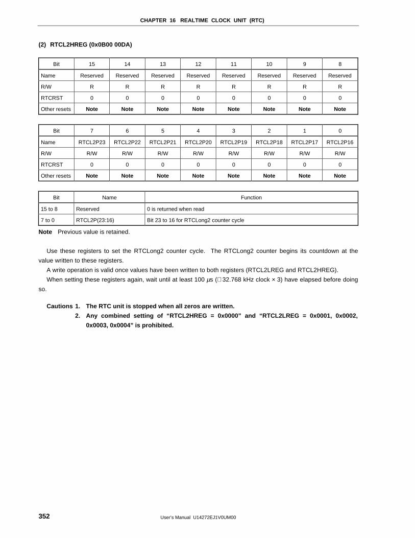
CHAPTER 16 REALTIME CLOCK UNIT (RTC)
User’s Manual U14272EJ1V0UM00352
(2) RTCL2HREG (0x0B00 00DA)
Bit 15 14 13 12 11 10 9 8
Name Reserved Reserved Reserved Reserved Reserved Reserved Reserved Reserved
R/W R R R R R R R R
RTCRST 0 0 0 0 0 0 0 0
Other resets Note Note Note Note Note Note Note Note
Bit 7 6 5 4 3 2 1 0
Name RTCL2P23 RTCL2P22 RTCL2P21 RTCL2P20 RTCL2P19 RTCL2P18 RTCL2P17 RTCL2P16
R/W R/W R/W R/W R/W R/W R/W R/W R/W
RTCRST 0 0 0 0 0 0 0 0
Other resets Note Note Note Note Note Note Note Note
Bit Name Function
15 to 8 Reserved 0 is returned when read
7 to 0 RTCL2P(23:16) Bit 23 to 16 for RTCLong2 counter cycle
Note Previous value is retained.
Use these registers to set the RTCLong2 counter cycle. The RTCLong2 counter begins its countdown at the
value written to these registers.
A write operation is valid once values have been written to both registers (RTCL2LREG and RTCL2HREG).
When setting these registers again, wait until at least 100 µs (≅ 32.768 kHz clock × 3) have elapsed before doing
so.
Cautions 1. The RTC unit is stopped when all zeros are written.
2. Any combined setting of “RTCL2HREG = 0x0000” and “RTCL2LREG = 0x0001, 0x0002,
0x0003, 0x0004” is prohibited.
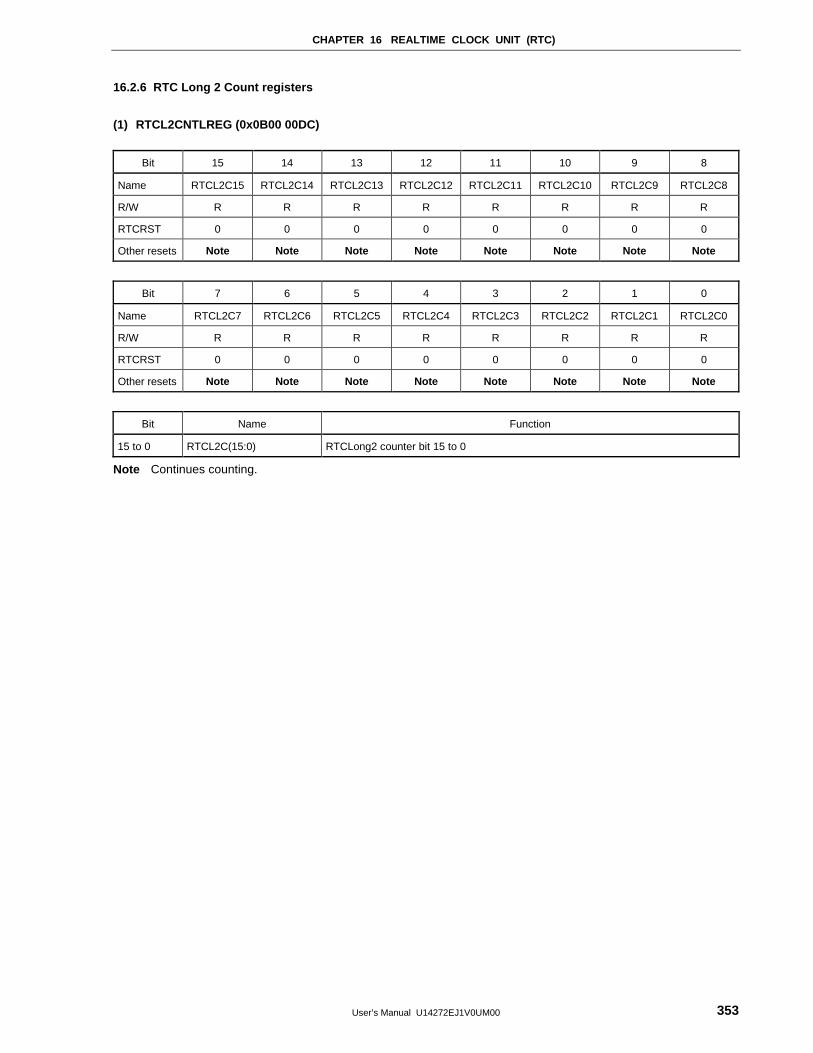
CHAPTER 16 REALTIME CLOCK UNIT (RTC)
User’s Manual U14272EJ1V0UM00 353
16.2.6 RTC Long 2 Count registers
(1) RTCL2CNTLREG (0x0B00 00DC)
Bit 15 14 13 12 11 10 9 8
Name RTCL2C15 RTCL2C14 RTCL2C13 RTCL2C12 RTCL2C11 RTCL2C10 RTCL2C9 RTCL2C8
R/W R R R R R R R R
RTCRST 0 0 0 0 0 0 0 0
Other resets Note Note Note Note Note Note Note Note
Bit 7 6 5 4 3 2 1 0
Name RTCL2C7 RTCL2C6 RTCL2C5 RTCL2C4 RTCL2C3 RTCL2C2 RTCL2C1 RTCL2C0
R/W R R R R R R R R
RTCRST 0 0 0 0 0 0 0 0
Other resets Note Note Note Note Note Note Note Note
Bit Name Function
15 to 0 RTCL2C(15:0) RTCLong2 counter bit 15 to 0
Note Continues counting.
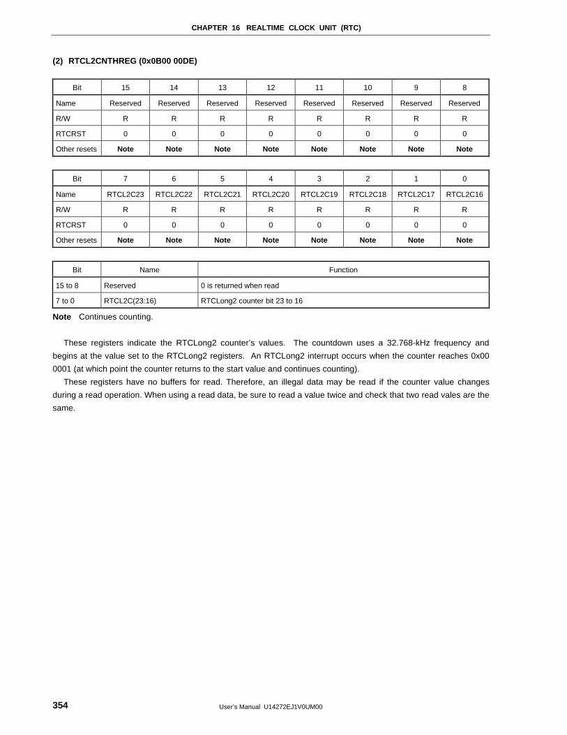
CHAPTER 16 REALTIME CLOCK UNIT (RTC)
User’s Manual U14272EJ1V0UM00354
(2) RTCL2CNTHREG (0x0B00 00DE)
Bit 15 14 13 12 11 10 9 8
Name Reserved Reserved Reserved Reserved Reserved Reserved Reserved Reserved
R/W R R R R R R R R
RTCRST 0 0 0 0 0 0 0 0
Other resets Note Note Note Note Note Note Note Note
Bit 7 6 5 4 3 2 1 0
Name RTCL2C23 RTCL2C22 RTCL2C21 RTCL2C20 RTCL2C19 RTCL2C18 RTCL2C17 RTCL2C16
R/W R R R R R R R R
RTCRST 0 0 0 0 0 0 0 0
Other resets Note Note Note Note Note Note Note Note
Bit Name Function
15 to 8 Reserved 0 is returned when read
7 to 0 RTCL2C(23:16) RTCLong2 counter bit 23 to 16
Note Continues counting.
These registers indicate the RTCLong2 counter’s values. The countdown uses a 32.768-kHz frequency and
begins at the value set to the RTCLong2 registers. An RTCLong2 interrupt occurs when the counter reaches 0x00
0001 (at which point the counter returns to the start value and continues counting).
These registers have no buffers for read. Therefore, an illegal data may be read if the counter value changes
during a read operation. When using a read data, be sure to read a value twice and check that two read vales are the
same.
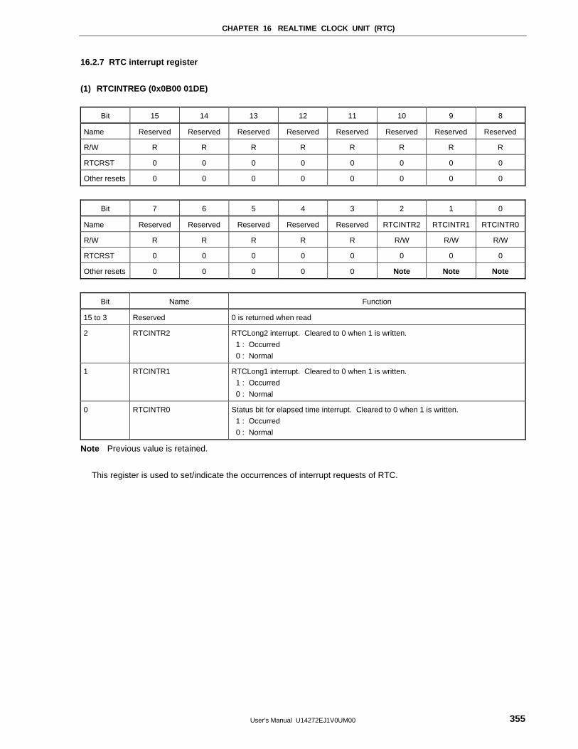
CHAPTER 16 REALTIME CLOCK UNIT (RTC)
User’s Manual U14272EJ1V0UM00 355
16.2.7 RTC interrupt register
(1) RTCINTREG (0x0B00 01DE)
Bit 15 14 13 12 11 10 9 8
Name Reserved Reserved Reserved Reserved Reserved Reserved Reserved Reserved
R/W R R R R R R R R
RTCRST 0 0 0 0 0 0 0 0
Other resets 0 0 0 0 0 0 0 0
Bit 7 6 5 4 3 2 1 0
Name Reserved Reserved Reserved Reserved Reserved RTCINTR2 RTCINTR1 RTCINTR0
R/W R R R R R R/W R/W R/W
RTCRST 0 0 0 0 0 0 0 0
Other resets 0 0 0 0 0 Note Note Note
Bit Name Function
15 to 3 Reserved 0 is returned when read
2 RTCINTR2 RTCLong2 interrupt. Cleared to 0 when 1 is written.
1 : Occurred
0 : Normal
1 RTCINTR1 RTCLong1 interrupt. Cleared to 0 when 1 is written.
1 : Occurred
0 : Normal
0 RTCINTR0 Status bit for elapsed time interrupt. Cleared to 0 when 1 is written.
1 : Occurred
0 : Normal
Note Previous value is retained.
This register is used to set/indicate the occurrences of interrupt requests of RTC.

User’s Manual U14272EJ1V0UM00356
[MEMO]
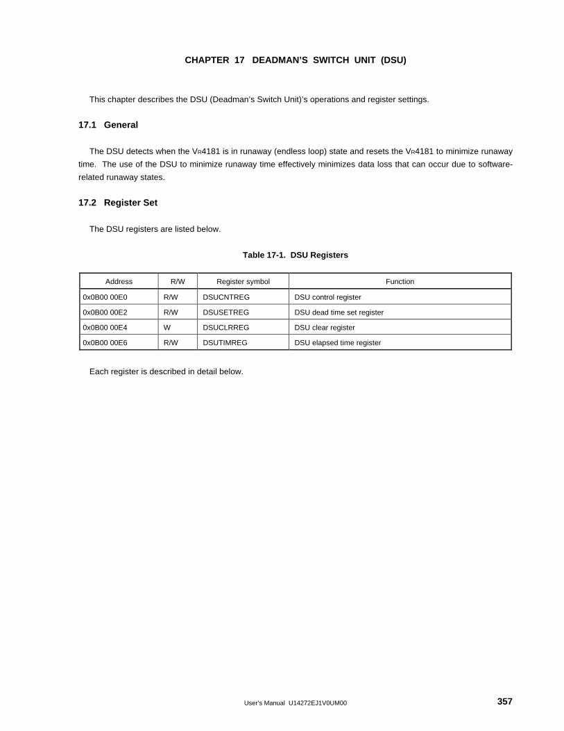
User’s Manual U14272EJ1V0UM00 357
CHAPTER 17 DEADMAN’S SWITCH UNIT (DSU)
This chapter describes the DSU (Deadman’s Switch Unit)’s operations and register settings.
17.1 General
The DSU detects when the VR4181 is in runaway (endless loop) state and resets the VR4181 to minimize runaway
time. The use of the DSU to minimize runaway time effectively minimizes data loss that can occur due to software-
related runaway states.
17.2 Register Set
The DSU registers are listed below.
Table 17-1. DSU Registers
Address R/W Register symbol Function
0x0B00 00E0 R/W DSUCNTREG DSU control register
0x0B00 00E2 R/W DSUSETREG DSU dead time set register
0x0B00 00E4 W DSUCLRREG DSU clear register
0x0B00 00E6 R/W DSUTIMREG DSU elapsed time register
Each register is described in detail below.
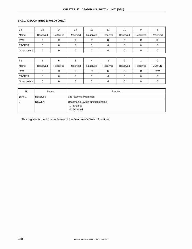
CHAPTER 17 DEADMAN’S SWITCH UNIT (DSU)
User’s Manual U14272EJ1V0UM00358
17.2.1 DSUCNTREG (0x0B00 00E0)
Bit 15 14 13 12 11 10 9 8
Name Reserved Reserved Reserved Reserved Reserved Reserved Reserved Reserved
R/W R R R R R R R R
RTCRST 0 0 0 0 0 0 0 0
Other resets 0 0 0 0 0 0 0 0
Bit 7 6 5 4 3 2 1 0
Name Reserved Reserved Reserved Reserved Reserved Reserved Reserved DSWEN
R/W R R R R R R R R/W
RTCRST 0 0 0 0 0 0 0 0
Other resets 0 0 0 0 0 0 0 0
Bit Name Function
15 to 1 Reserved 0 is returned when read
0 DSWEN Deadman’s Switch function enable
1 : Enabled
0 : Disabled
This register is used to enable use of the Deadman’s Switch functions.
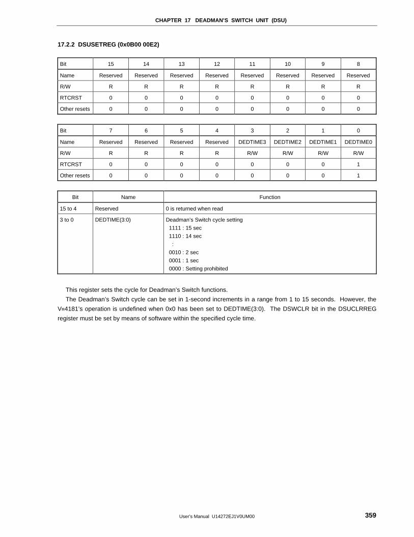
CHAPTER 17 DEADMAN’S SWITCH UNIT (DSU)
User’s Manual U14272EJ1V0UM00 359
17.2.2 DSUSETREG (0x0B00 00E2)
Bit 15 14 13 12 11 10 9 8
Name Reserved Reserved Reserved Reserved Reserved Reserved Reserved Reserved
R/W R R R R R R R R
RTCRST 0 0 0 0 0 0 0 0
Other resets 0 0 0 0 0 0 0 0
Bit 7 6 5 4 3 2 1 0
Name Reserved Reserved Reserved Reserved DEDTIME3 DEDTIME2 DEDTIME1 DEDTIME0
R/W R R R R R/W R/W R/W R/W
RTCRST 0 0 0 0 0 0 0 1
Other resets 0 0 0 0 0 0 0 1
Bit Name Function
15 to 4 Reserved 0 is returned when read
3 to 0 DEDTIME(3:0) Deadman’s Switch cycle setting
1111 : 15 sec
1110 : 14 sec
:
0010 : 2 sec
0001 : 1 sec
0000 : Setting prohibited
This register sets the cycle for Deadman’s Switch functions.
The Deadman’s Switch cycle can be set in 1-second increments in a range from 1 to 15 seconds. However, the
VR4181’s operation is undefined when 0x0 has been set to DEDTIME(3:0). The DSWCLR bit in the DSUCLRREG
register must be set by means of software within the specified cycle time.
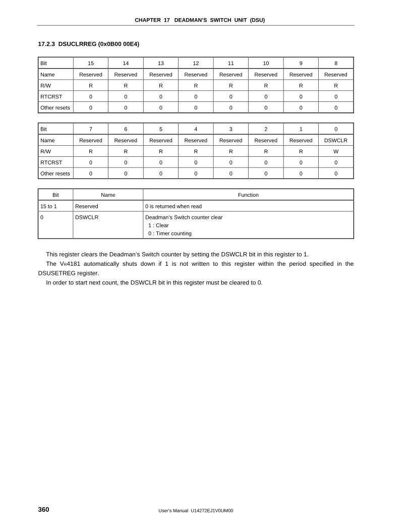
CHAPTER 17 DEADMAN’S SWITCH UNIT (DSU)
User’s Manual U14272EJ1V0UM00360
17.2.3 DSUCLRREG (0x0B00 00E4)
Bit 15 14 13 12 11 10 9 8
Name Reserved Reserved Reserved Reserved Reserved Reserved Reserved Reserved
R/W R R R R R R R R
RTCRST 0 0 0 0 0 0 0 0
Other resets 0 0 0 0 0 0 0 0
Bit 7 6 5 4 3 2 1 0
Name Reserved Reserved Reserved Reserved Reserved Reserved Reserved DSWCLR
R/W R R R R R R R W
RTCRST 0 0 0 0 0 0 0 0
Other resets 0 0 0 0 0 0 0 0
Bit Name Function
15 to 1 Reserved 0 is returned when read
0 DSWCLR Deadman’s Switch counter clear
1 : Clear
0 : Timer counting
This register clears the Deadman’s Switch counter by setting the DSWCLR bit in this register to 1.
The VR4181 automatically shuts down if 1 is not written to this register within the period specified in the
DSUSETREG register.
In order to start next count, the DSWCLR bit in this register must be cleared to 0.
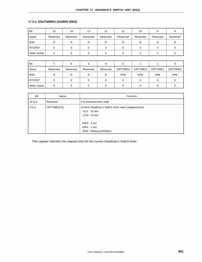
CHAPTER 17 DEADMAN’S SWITCH UNIT (DSU)
User’s Manual U14272EJ1V0UM00 361
17.2.4 DSUTIMREG (0x0B00 00E6)
Bit 15 14 13 12 11 10 9 8
Name Reserved Reserved Reserved Reserved Reserved Reserved Reserved Reserved
R/W R R R R R R R R
RTCRST 0 0 0 0 0 0 0 0
Other resets 0 0 0 0 0 0 0 0
Bit 7 6 5 4 3 2 1 0
Name Reserved Reserved Reserved Reserved CRTTIME3 CRTTIME2 CRTTIME1 CRTTIME0
R/W R R R R R/W R/W R/W R/W
RTCRST 0 0 0 0 0 0 0 0
Other resets 0 0 0 0 0 0 0 0
Bit Name Function
15 to 4 Reserved 0 is returned when read
3 to 0 CRTTIME(3:0) Current Deadman’s Switch timer value (elapsed time)
1111 : 15 sec
1110 : 14 sec
:
0010 : 2 sec
0001 : 1 sec
0000 : Setting prohibited
This register indicates the elapsed time for the current Deadman’s Switch timer.
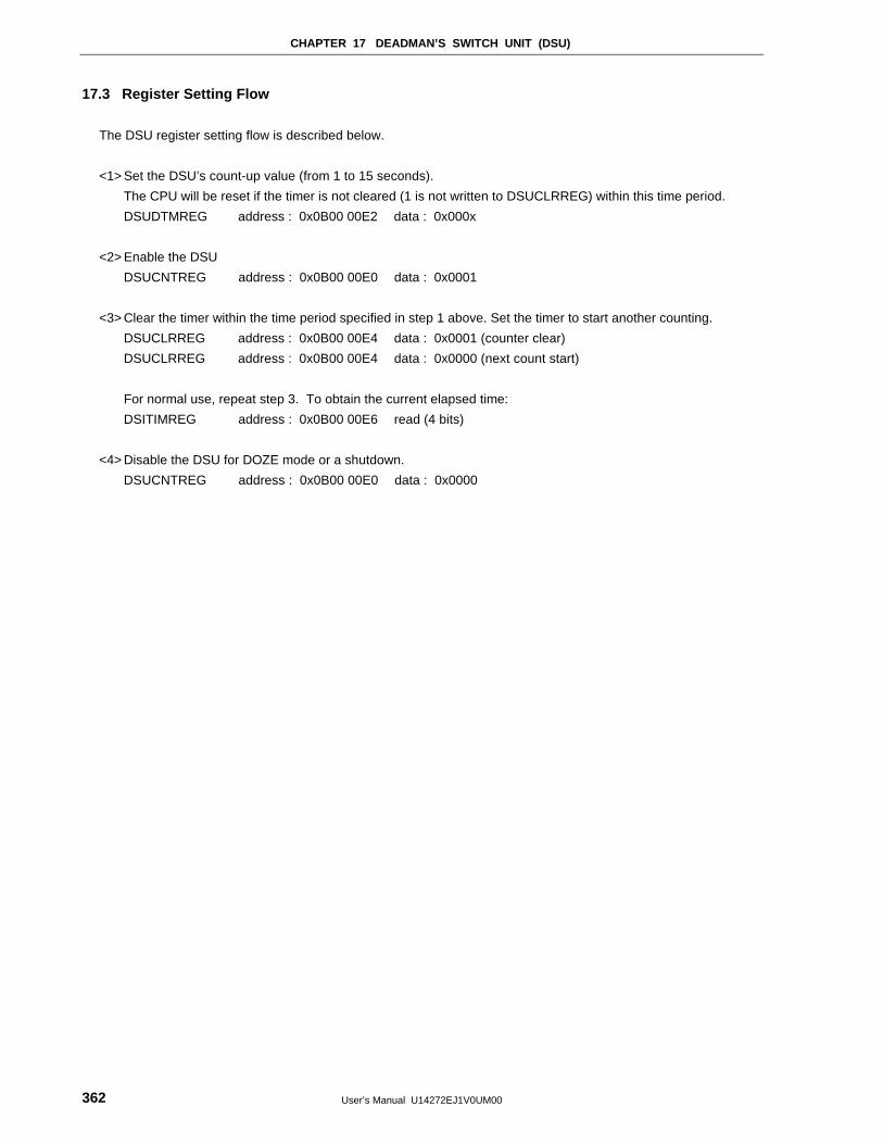
CHAPTER 17 DEADMAN’S SWITCH UNIT (DSU)
User’s Manual U14272EJ1V0UM00362
17.3 Register Setting Flow
The DSU register setting flow is described below.
<1> Set the DSU’s count-up value (from 1 to 15 seconds).
The CPU will be reset if the timer is not cleared (1 is not written to DSUCLRREG) within this time period.
DSUDTMREG address : 0x0B00 00E2 data : 0x000x
<2> Enable the DSU
DSUCNTREG address : 0x0B00 00E0 data : 0x0001
<3> Clear the timer within the time period specified in step 1 above. Set the timer to start another counting.
DSUCLRREG address : 0x0B00 00E4 data : 0x0001 (counter clear)
DSUCLRREG address : 0x0B00 00E4 data : 0x0000 (next count start)
For normal use, repeat step 3. To obtain the current elapsed time:
DSITIMREG address : 0x0B00 00E6 read (4 bits)
<4> Disable the DSU for DOZE mode or a shutdown.
DSUCNTREG address : 0x0B00 00E0 data : 0x0000
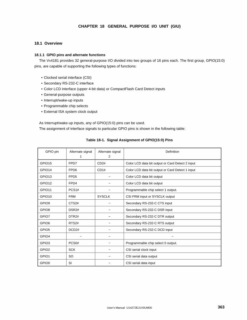
User’s Manual U14272EJ1V0UM00 363
CHAPTER 18 GENERAL PURPOSE I/O UNIT (GIU)
18.1 Overview
18.1.1 GPIO pins and alternate functions
The VR4181 provides 32 general-purpose I/O divided into two groups of 16 pins each. The first group, GPIO(15:0)
pins, are capable of supporting the following types of functions:
• Clocked serial interface (CSI)
• Secondary RS-232-C interface
• Color LCD interface (upper 4-bit data) or CompactFlash Card Detect inputs
• General-purpose outputs
• Interrupt/wake-up inputs
• Programmable chip selects
• External ISA system clock output
As Interrupt/wake-up inputs, any of GPIO(15:0) pins can be used.
The assignment of interface signals to particular GPIO pins is shown in the following table:
Table 18-1. Signal Assignment of GPIO(15:0) Pins
GPIO pin Alternate signal
1
Alternate signal
2
Definition
GPIO15 FPD7 CD2# Color LCD data bit output or Card Detect 2 input
GPIO14 FPD6 CD1# Color LCD data bit output or Card Detect 1 input
GPIO13 FPD5 − Color LCD data bit output
GPIO12 FPD4 − Color LCD data bit output
GPIO11 PCS1# − Programmable chip select 1 output.
GPIO10 FRM SYSCLK CSI FRM input or SYSCLK output
GPIO9 CTS2# − Secondary RS-232-C CTS input
GPIO8 DSR2# − Secondary RS-232-C DSR input
GPIO7 DTR2# − Secondary RS-232-C DTR output
GPIO6 RTS2# − Secondary RS-232-C RTS output
GPIO5 DCD2# − Secondary RS-232-C DCD input
GPIO4 − − −
GPIO3 PCS0# − Programmable chip select 0 output.
GPIO2 SCK − CSI serial clock input
GPIO1 SO − CSI serial data output
GPIO0 SI − CSI serial data input
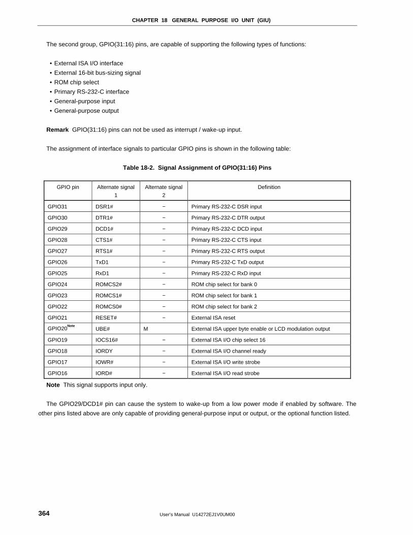
CHAPTER 18 GENERAL PURPOSE I/O UNIT (GIU)
User’s Manual U14272EJ1V0UM00364
The second group, GPIO(31:16) pins, are capable of supporting the following types of functions:
• External ISA I/O interface
• External 16-bit bus-sizing signal
• ROM chip select
• Primary RS-232-C interface
• General-purpose input
• General-purpose output
Remark GPIO(31:16) pins can not be used as interrupt / wake-up input.
The assignment of interface signals to particular GPIO pins is shown in the following table:
Table 18-2. Signal Assignment of GPIO(31:16) Pins
GPIO pin Alternate signal
1
Alternate signal
2
Definition
GPIO31 DSR1# − Primary RS-232-C DSR input
GPIO30 DTR1# − Primary RS-232-C DTR output
GPIO29 DCD1# − Primary RS-232-C DCD input
GPIO28 CTS1# − Primary RS-232-C CTS input
GPIO27 RTS1# − Primary RS-232-C RTS output
GPIO26 TxD1 − Primary RS-232-C TxD output
GPIO25 RxD1 − Primary RS-232-C RxD input
GPIO24 ROMCS2# − ROM chip select for bank 0
GPIO23 ROMCS1# − ROM chip select for bank 1
GPIO22 ROMCS0# − ROM chip select for bank 2
GPIO21 RESET# − External ISA reset
GPIO20Note
UBE# M External ISA upper byte enable or LCD modulation output
GPIO19 IOCS16# − External ISA I/O chip select 16
GPIO18 IORDY − External ISA I/O channel ready
GPIO17 IOWR# − External ISA I/O write strobe
GPIO16 IORD# − External ISA I/O read strobe
Note This signal supports input only.
The GPIO29/DCD1# pin can cause the system to wake-up from a low power mode if enabled by software. The
other pins listed above are only capable of providing general-purpose input or output, or the optional function listed.
CHAPTER 18 GENERAL PURPOSE I/O UNIT (GIU)
User’s Manual U14272EJ1V0UM00 365
18.1.2 Pin direction control
For each GPIO pin, the GIU provides one buffer enable, GPENn, one output data, GPOn, and one input data,
GPIn. The function of each GPIO pin is decoded by 2 register bits in one of the GPIO Mode registers. The most
significant bit, GPnMD1, controls the direction of the GPIO pin while the system is powered (Fullspeed, Standby, and
Suspend modes). When this bit is set to 1, the GPIO pin is normally configured as an output.
During Hibernate mode, the GPIO buffer enables are controlled by the GPHIBSTH and GPHIBSTL registers.
Remark n = 0 to 31
18.1.3 Non-volatile registers
The GIU includes sixteen 16-bit general-purpose battery-backed registers. These registers can be used by system
software to save the state of selected registers located in the 2.5V core prior to entering Hibernate mode. Once a
wake-up event occurs, system software can then restore the state of those 2.5V registers from the general-purpose
battery-backed registers.
The battery-backed registers are located in the address range of 0x0B00 0330 to 0x0B00 034F.
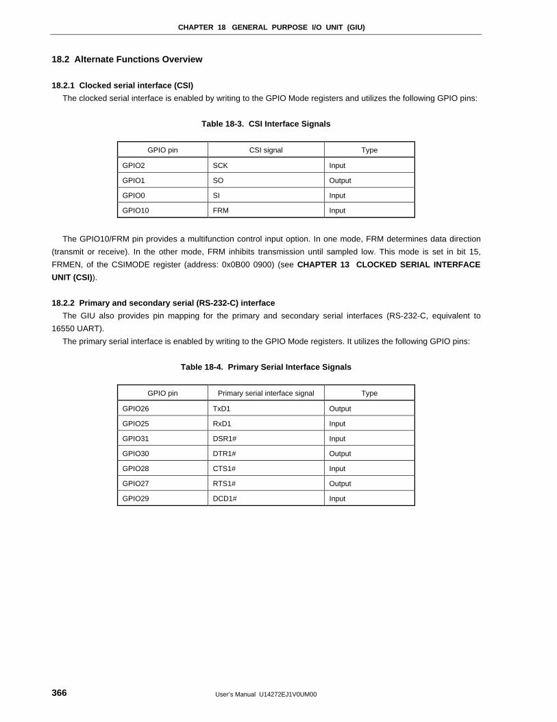
CHAPTER 18 GENERAL PURPOSE I/O UNIT (GIU)
User’s Manual U14272EJ1V0UM00366
18.2 Alternate Functions Overview
18.2.1 Clocked serial interface (CSI)
The clocked serial interface is enabled by writing to the GPIO Mode registers and utilizes the following GPIO pins:
Table 18-3. CSI Interface Signals
GPIO pin CSI signal Type
GPIO2 SCK Input
GPIO1 SO Output
GPIO0 SI Input
GPIO10 FRM Input
The GPIO10/FRM pin provides a multifunction control input option. In one mode, FRM determines data direction
(transmit or receive). In the other mode, FRM inhibits transmission until sampled low. This mode is set in bit 15,
FRMEN, of the CSIMODE register (address: 0x0B00 0900) (see CHAPTER 13 CLOCKED SERIAL INTERFACE
UNIT (CSI)).
18.2.2 Primary and secondary serial (RS-232-C) interface
The GIU also provides pin mapping for the primary and secondary serial interfaces (RS-232-C, equivalent to
16550 UART).
The primary serial interface is enabled by writing to the GPIO Mode registers. It utilizes the following GPIO pins:
Table 18-4. Primary Serial Interface Signals
GPIO pin Primary serial interface signal Type
GPIO26 TxD1 Output
GPIO25 RxD1 Input
GPIO31 DSR1# Input
GPIO30 DTR1# Output
GPIO28 CTS1# Input
GPIO27 RTS1# Output
GPIO29 DCD1# Input
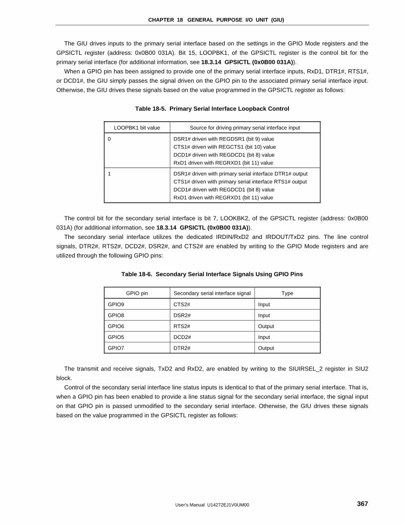
CHAPTER 18 GENERAL PURPOSE I/O UNIT (GIU)
User’s Manual U14272EJ1V0UM00 367
The GIU drives inputs to the primary serial interface based on the settings in the GPIO Mode registers and the
GPSICTL register (address: 0x0B00 031A). Bit 15, LOOPBK1, of the GPSICTL register is the control bit for the
primary serial interface (for additional information, see 18.3.14 GPSICTL (0x0B00 031A) ).
When a GPIO pin has been assigned to provide one of the primary serial interface inputs, RxD1, DTR1#, RTS1#,
or DCD1#, the GIU simply passes the signal driven on the GPIO pin to the associated primary serial interface input.
Otherwise, the GIU drives these signals based on the value programmed in the GPSICTL register as follows:
Table 18-5. Primary Serial Interface Loopback Control
LOOPBK1 bit value Source for driving primary serial interface input
0 DSR1# driven with REGDSR1 (bit 9) value
CTS1# driven with REGCTS1 (bit 10) value
DCD1# driven with REGDCD1 (bit 8) value
RxD1 driven with REGRXD1 (bit 11) value
1 DSR1# driven with primary serial interface DTR1# output
CTS1# driven with primary serial interface RTS1# output
DCD1# driven with REGDCD1 (bit 8) value
RxD1 driven with REGRXD1 (bit 11) value
The control bit for the secondary serial interface is bit 7, LOOKBK2, of the GPSICTL register (address: 0x0B00
031A) (for additional information, see 18.3.14 GPSICTL (0x0B00 031A) ).
The secondary serial interface utilizes the dedicated IRDIN/RxD2 and IRDOUT/TxD2 pins. The line control
signals, DTR2#, RTS2#, DCD2#, DSR2#, and CTS2# are enabled by writing to the GPIO Mode registers and are
utilized through the following GPIO pins:
Table 18-6. Secondary Serial Interface Signals Using GPIO Pins
GPIO pin Secondary serial interface signal Type
GPIO9 CTS2# Input
GPIO8 DSR2# Input
GPIO6 RTS2# Output
GPIO5 DCD2# Input
GPIO7 DTR2# Output
The transmit and receive signals, TxD2 and RxD2, are enabled by writing to the SIUIRSEL_2 register in SIU2
block.
Control of the secondary serial interface line status inputs is identical to that of the primary serial interface. That is,
when a GPIO pin has been enabled to provide a line status signal for the secondary serial interface, the signal input
on that GPIO pin is passed unmodified to the secondary serial interface. Otherwise, the GIU drives these signals
based on the value programmed in the GPSICTL register as follows:
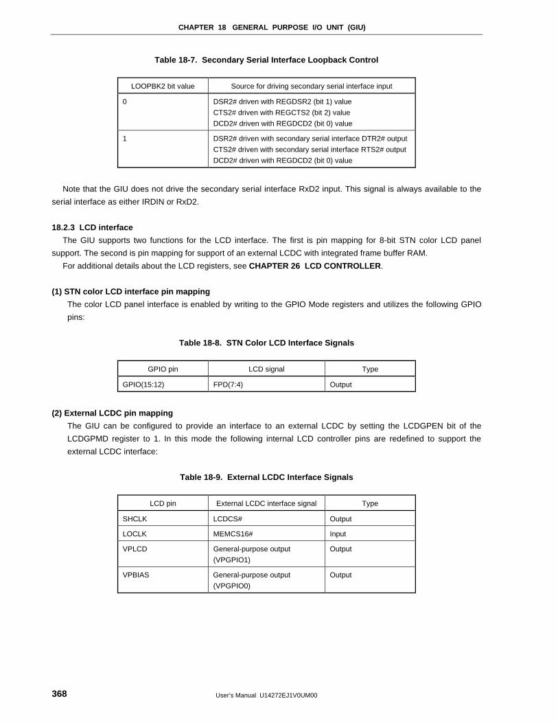
CHAPTER 18 GENERAL PURPOSE I/O UNIT (GIU)
User’s Manual U14272EJ1V0UM00368
Table 18-7. Secondary Serial Interface Loopback Control
LOOPBK2 bit value Source for driving secondary serial interface input
0 DSR2# driven with REGDSR2 (bit 1) value
CTS2# driven with REGCTS2 (bit 2) value
DCD2# driven with REGDCD2 (bit 0) value
1 DSR2# driven with secondary serial interface DTR2# output
CTS2# driven with secondary serial interface RTS2# output
DCD2# driven with REGDCD2 (bit 0) value
Note that the GIU does not drive the secondary serial interface RxD2 input. This signal is always available to the
serial interface as either IRDIN or RxD2.
18.2.3 LCD interface
The GIU supports two functions for the LCD interface. The first is pin mapping for 8-bit STN color LCD panel
support. The second is pin mapping for support of an external LCDC with integrated frame buffer RAM.
For additional details about the LCD registers, see CHAPTER 26 LCD CONTROLLER .
(1) STN color LCD interface pin mapping
The color LCD panel interface is enabled by writing to the GPIO Mode registers and utilizes the following GPIO
pins:
Table 18-8. STN Color LCD Interface Signals
GPIO pin LCD signal Type
GPIO(15:12) FPD(7:4) Output
(2) External LCDC pin mapping
The GIU can be configured to provide an interface to an external LCDC by setting the LCDGPEN bit of the
LCDGPMD register to 1. In this mode the following internal LCD controller pins are redefined to support the
external LCDC interface:
Table 18-9. External LCDC Interface Signals
LCD pin External LCDC interface signal Type
SHCLK LCDCS# Output
LOCLK MEMCS16# Input
VPLCD General-purpose output
(VPGPIO1)
Output
VPBIAS General-purpose output
(VPGPIO0)
Output
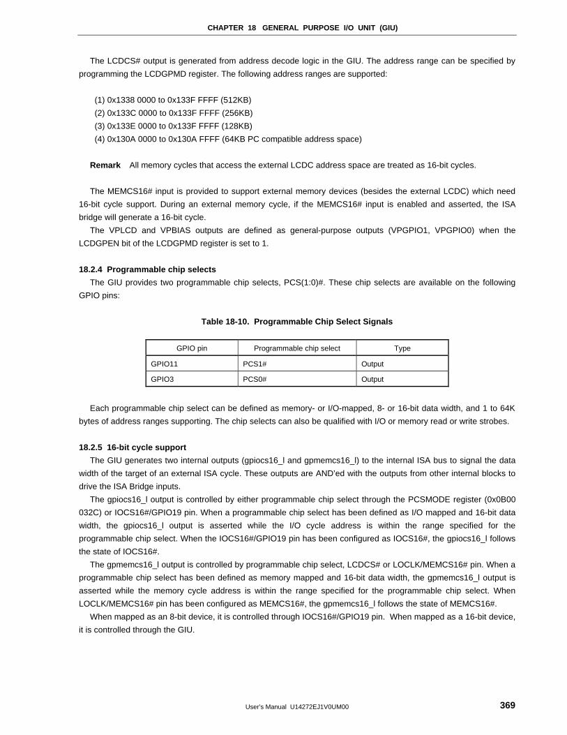
CHAPTER 18 GENERAL PURPOSE I/O UNIT (GIU)
User’s Manual U14272EJ1V0UM00 369
The LCDCS# output is generated from address decode logic in the GIU. The address range can be specified by
programming the LCDGPMD register. The following address ranges are supported:
(1) 0x1338 0000 to 0x133F FFFF (512KB)
(2) 0x133C 0000 to 0x133F FFFF (256KB)
(3) 0x133E 0000 to 0x133F FFFF (128KB)
(4) 0x130A 0000 to 0x130A FFFF (64KB PC compatible address space)
Remark All memory cycles that access the external LCDC address space are treated as 16-bit cycles.
The MEMCS16# input is provided to support external memory devices (besides the external LCDC) which need
16-bit cycle support. During an external memory cycle, if the MEMCS16# input is enabled and asserted, the ISA
bridge will generate a 16-bit cycle.
The VPLCD and VPBIAS outputs are defined as general-purpose outputs (VPGPIO1, VPGPIO0) when the
LCDGPEN bit of the LCDGPMD register is set to 1.
18.2.4 Programmable chip selects
The GIU provides two programmable chip selects, PCS(1:0)#. These chip selects are available on the following
GPIO pins:
Table 18-10. Programmable Chip Select Signals
GPIO pin Programmable chip select Type
GPIO11 PCS1# Output
GPIO3 PCS0# Output
Each programmable chip select can be defined as memory- or I/O-mapped, 8- or 16-bit data width, and 1 to 64K
bytes of address ranges supporting. The chip selects can also be qualified with I/O or memory read or write strobes.
18.2.5 16-bit cycle support
The GIU generates two internal outputs (gpiocs16_l and gpmemcs16_l) to the internal ISA bus to signal the data
width of the target of an external ISA cycle. These outputs are AND’ed with the outputs from other internal blocks to
drive the ISA Bridge inputs.
The gpiocs16_l output is controlled by either programmable chip select through the PCSMODE register (0x0B00
032C) or IOCS16#/GPIO19 pin. When a programmable chip select has been defined as I/O mapped and 16-bit data
width, the gpiocs16_l output is asserted while the I/O cycle address is within the range specified for the
programmable chip select. When the IOCS16#/GPIO19 pin has been configured as IOCS16#, the gpiocs16_l follows
the state of IOCS16#.
The gpmemcs16_l output is controlled by programmable chip select, LCDCS# or LOCLK/MEMCS16# pin. When a
programmable chip select has been defined as memory mapped and 16-bit data width, the gpmemcs16_l output is
asserted while the memory cycle address is within the range specified for the programmable chip select. When
LOCLK/MEMCS16# pin has been configured as MEMCS16#, the gpmemcs16_l follows the state of MEMCS16#.
When mapped as an 8-bit device, it is controlled through IOCS16#/GPIO19 pin. When mapped as a 16-bit device,
it is controlled through the GIU.
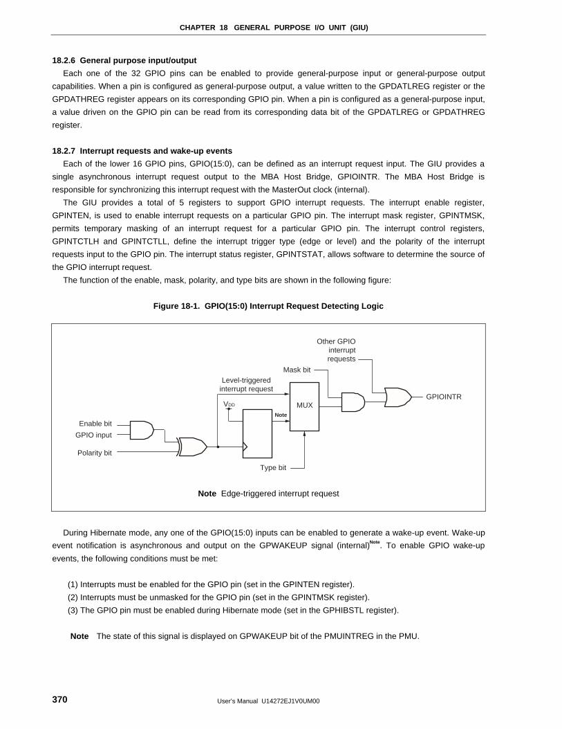
CHAPTER 18 GENERAL PURPOSE I/O UNIT (GIU)
User’s Manual U14272EJ1V0UM00370
18.2.6 General purpose input/output
Each one of the 32 GPIO pins can be enabled to provide general-purpose input or general-purpose output
capabilities. When a pin is configured as general-purpose output, a value written to the GPDATLREG register or the
GPDATHREG register appears on its corresponding GPIO pin. When a pin is configured as a general-purpose input,
a value driven on the GPIO pin can be read from its corresponding data bit of the GPDATLREG or GPDATHREG
register.
18.2.7 Interrupt requests and wake-up events
Each of the lower 16 GPIO pins, GPIO(15:0), can be defined as an interrupt request input. The GIU provides a
single asynchronous interrupt request output to the MBA Host Bridge, GPIOINTR. The MBA Host Bridge is
responsible for synchronizing this interrupt request with the MasterOut clock (internal).
The GIU provides a total of 5 registers to support GPIO interrupt requests. The interrupt enable register,
GPINTEN, is used to enable interrupt requests on a particular GPIO pin. The interrupt mask register, GPINTMSK,
permits temporary masking of an interrupt request for a particular GPIO pin. The interrupt control registers,
GPINTCTLH and GPINTCTLL, define the interrupt trigger type (edge or level) and the polarity of the interrupt
requests input to the GPIO pin. The interrupt status register, GPINTSTAT, allows software to determine the source of
the GPIO interrupt request.
The function of the enable, mask, polarity, and type bits are shown in the following figure:
Figure 18-1. GPIO(15:0) Interrupt Request Detecting Logic
Enable bit
GPIO input
Polarity bit
Type bit
Mask bit
Other GPIOinterrupt
requests
GPIOINTRMUXVDD
Level-triggeredinterrupt request
Note
Note Edge-triggered interrupt request
During Hibernate mode, any one of the GPIO(15:0) inputs can be enabled to generate a wake-up event. Wake-up
event notification is asynchronous and output on the GPWAKEUP signal (internal)Note. To enable GPIO wake-up
events, the following conditions must be met:
(1) Interrupts must be enabled for the GPIO pin (set in the GPINTEN register).
(2) Interrupts must be unmasked for the GPIO pin (set in the GPINTMSK register).
(3) The GPIO pin must be enabled during Hibernate mode (set in the GPHIBSTL register).
Note The state of this signal is displayed on GPWAKEUP bit of the PMUINTREG in the PMU.
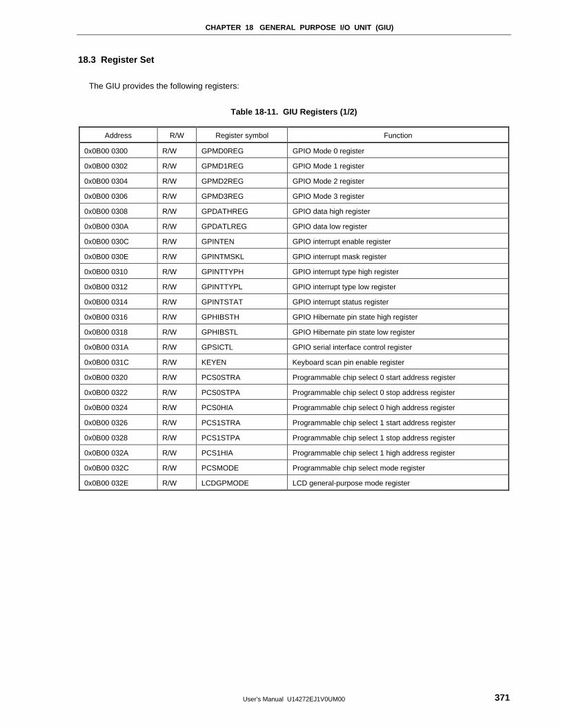
CHAPTER 18 GENERAL PURPOSE I/O UNIT (GIU)
User’s Manual U14272EJ1V0UM00 371
18.3 Register Set
The GIU provides the following registers:
Table 18-11. GIU Registers (1/2)
Address R/W Register symbol Function
0x0B00 0300 R/W GPMD0REG GPIO Mode 0 register
0x0B00 0302 R/W GPMD1REG GPIO Mode 1 register
0x0B00 0304 R/W GPMD2REG GPIO Mode 2 register
0x0B00 0306 R/W GPMD3REG GPIO Mode 3 register
0x0B00 0308 R/W GPDATHREG GPIO data high register
0x0B00 030A R/W GPDATLREG GPIO data low register
0x0B00 030C R/W GPINTEN GPIO interrupt enable register
0x0B00 030E R/W GPINTMSKL GPIO interrupt mask register
0x0B00 0310 R/W GPINTTYPH GPIO interrupt type high register
0x0B00 0312 R/W GPINTTYPL GPIO interrupt type low register
0x0B00 0314 R/W GPINTSTAT GPIO interrupt status register
0x0B00 0316 R/W GPHIBSTH GPIO Hibernate pin state high register
0x0B00 0318 R/W GPHIBSTL GPIO Hibernate pin state low register
0x0B00 031A R/W GPSICTL GPIO serial interface control register
0x0B00 031C R/W KEYEN Keyboard scan pin enable register
0x0B00 0320 R/W PCS0STRA Programmable chip select 0 start address register
0x0B00 0322 R/W PCS0STPA Programmable chip select 0 stop address register
0x0B00 0324 R/W PCS0HIA Programmable chip select 0 high address register
0x0B00 0326 R/W PCS1STRA Programmable chip select 1 start address register
0x0B00 0328 R/W PCS1STPA Programmable chip select 1 stop address register
0x0B00 032A R/W PCS1HIA Programmable chip select 1 high address register
0x0B00 032C R/W PCSMODE Programmable chip select mode register
0x0B00 032E R/W LCDGPMODE LCD general-purpose mode register
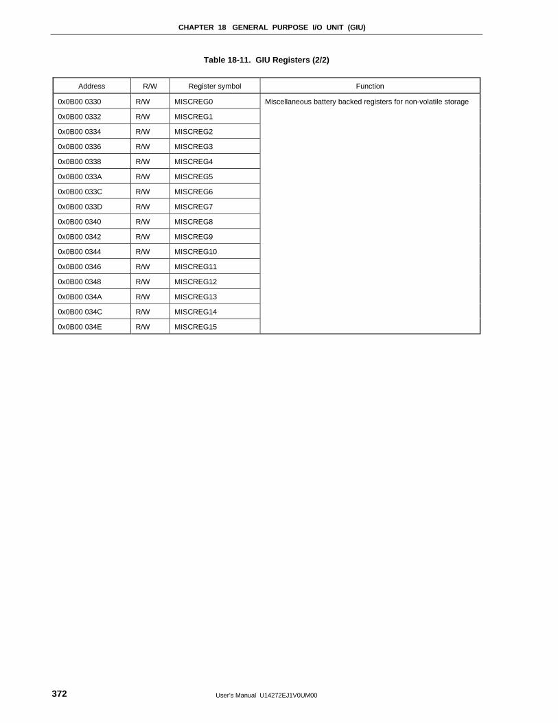
CHAPTER 18 GENERAL PURPOSE I/O UNIT (GIU)
User’s Manual U14272EJ1V0UM00372
Table 18-11. GIU Registers (2/2)
Address R/W Register symbol Function
0x0B00 0330 R/W MISCREG0
0x0B00 0332 R/W MISCREG1
0x0B00 0334 R/W MISCREG2
0x0B00 0336 R/W MISCREG3
0x0B00 0338 R/W MISCREG4
0x0B00 033A R/W MISCREG5
0x0B00 033C R/W MISCREG6
0x0B00 033D R/W MISCREG7
0x0B00 0340 R/W MISCREG8
0x0B00 0342 R/W MISCREG9
0x0B00 0344 R/W MISCREG10
0x0B00 0346 R/W MISCREG11
0x0B00 0348 R/W MISCREG12
0x0B00 034A R/W MISCREG13
0x0B00 034C R/W MISCREG14
0x0B00 034E R/W MISCREG15
Miscellaneous battery backed registers for non-volatile storage
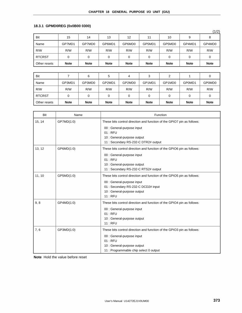
CHAPTER 18 GENERAL PURPOSE I/O UNIT (GIU)
User’s Manual U14272EJ1V0UM00 373
18.3.1 GPMD0REG (0x0B00 0300)
(1/2)
Bit 15 14 13 12 11 10 9 8
Name GP7MD1 GP7MD0 GP6MD1 GP6MD0 GP5MD1 GP5MD0 GP4MD1 GP4MD0
R/W R/W R/W R/W R/W R/W R/W R/W R/W
RTCRST 0 0 0 0 0 0 0 0
Other resets Note Note Note Note Note Note Note Note
Bit 7 6 5 4 3 2 1 0
Name GP3MD1 GP3MD0 GP2MD1 GP2MD0 GP1MD1 GP1MD0 GP0MD1 GP0MD0
R/W R/W R/W R/W R/W R/W R/W R/W R/W
RTCRST 0 0 0 0 0 0 0 0
Other resets Note Note Note Note Note Note Note Note
Bit Name Function
15, 14 GP7MD(1:0) These bits control direction and function of the GPIO7 pin as follows:
00 : General-purpose input
01 : RFU
10 : General-purpose output
11 : Secondary RS-232-C DTR2# output
13, 12 GP6MD(1:0) These bits control direction and function of the GPIO6 pin as follows:
00 : General-purpose input
01 : RFU
10 : General-purpose output
11 : Secondary RS-232-C RTS2# output
11, 10 GP5MD(1:0) These bits control direction and function of the GPIO5 pin as follows:
00 : General-purpose input
01 : Secondary RS-232-C DCD2# input
10 : General-purpose output
11 : RFU
9, 8 GP4MD(1:0) These bits control direction and function of the GPIO4 pin as follows:
00 : General-purpose input
01 : RFU
10 : General-purpose output
11 : RFU
7, 6 GP3MD(1:0) These bits control direction and function of the GPIO3 pin as follows:
00 : General-purpose input
01 : RFU
10 : General-purpose output
11 : Programmable chip select 0 output
Note Hold the value before reset

CHAPTER 18 GENERAL PURPOSE I/O UNIT (GIU)
User’s Manual U14272EJ1V0UM00374
(2/2)
Bit Name Function
5, 4 GP2MD(1:0) These bits control direction and function of the GPIO2 pin as follows:
00 : General-purpose input
01 : CSI SCK input
10 : General-purpose output
11 : RFU
3, 2 GP1MD(1:0) These bits control direction and function of the GPIO1 pin as follows:
00 : General-purpose input
01 : RFU
10 : General-purpose output
11 : CSI SO output
1, 0 GP0MD(1:0) These bits control direction and function of the GPIO0 pin as follows:
00 : General-purpose input
01 : CSI SI input
10 : General-purpose output
11 : RFU
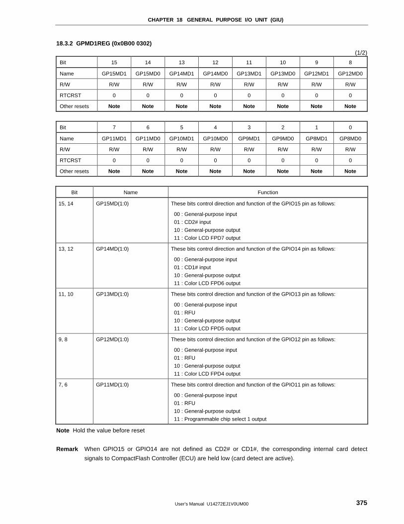
CHAPTER 18 GENERAL PURPOSE I/O UNIT (GIU)
User’s Manual U14272EJ1V0UM00 375
18.3.2 GPMD1REG (0x0B00 0302)
(1/2)
Bit 15 14 13 12 11 10 9 8
Name GP15MD1 GP15MD0 GP14MD1 GP14MD0 GP13MD1 GP13MD0 GP12MD1 GP12MD0
R/W R/W R/W R/W R/W R/W R/W R/W R/W
RTCRST 0 0 0 0 0 0 0 0
Other resets Note Note Note Note Note Note Note Note
Bit 7 6 5 4 3 2 1 0
Name GP11MD1 GP11MD0 GP10MD1 GP10MD0 GP9MD1 GP9MD0 GP8MD1 GP8MD0
R/W R/W R/W R/W R/W R/W R/W R/W R/W
RTCRST 0 0 0 0 0 0 0 0
Other resets Note Note Note Note Note Note Note Note
Bit Name Function
15, 14 GP15MD(1:0) These bits control direction and function of the GPIO15 pin as follows:
00 : General-purpose input
01 : CD2# input
10 : General-purpose output
11 : Color LCD FPD7 output
13, 12 GP14MD(1:0) These bits control direction and function of the GPIO14 pin as follows:
00 : General-purpose input
01 : CD1# input
10 : General-purpose output
11 : Color LCD FPD6 output
11, 10 GP13MD(1:0) These bits control direction and function of the GPIO13 pin as follows:
00 : General-purpose input
01 : RFU
10 : General-purpose output
11 : Color LCD FPD5 output
9, 8 GP12MD(1:0) These bits control direction and function of the GPIO12 pin as follows:
00 : General-purpose input
01 : RFU
10 : General-purpose output
11 : Color LCD FPD4 output
7, 6 GP11MD(1:0) These bits control direction and function of the GPIO11 pin as follows:
00 : General-purpose input
01 : RFU
10 : General-purpose output
11 : Programmable chip select 1 output
Note Hold the value before reset
Remark When GPIO15 or GPIO14 are not defined as CD2# or CD1#, the corresponding internal card detect
signals to CompactFlash Controller (ECU) are held low (card detect are active).
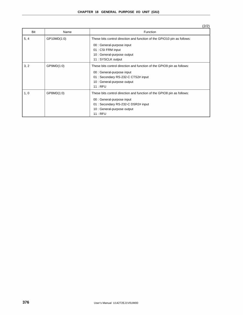
CHAPTER 18 GENERAL PURPOSE I/O UNIT (GIU)
User’s Manual U14272EJ1V0UM00376
(2/2)
Bit Name Function
5, 4 GP10MD(1:0) These bits control direction and function of the GPIO10 pin as follows:
00 : General-purpose input
01 : CSI FRM input
10 : General-purpose output
11 : SYSCLK output
3, 2 GP9MD(1:0) These bits control direction and function of the GPIO9 pin as follows:
00 : General-purpose input
01 : Secondary RS-232-C CTS2# input
10 : General-purpose output
11 : RFU
1, 0 GP8MD(1:0) These bits control direction and function of the GPIO8 pin as follows:
00 : General-purpose input
01 : Secondary RS-232-C DSR2# input
10 : General-purpose output
11 : RFU
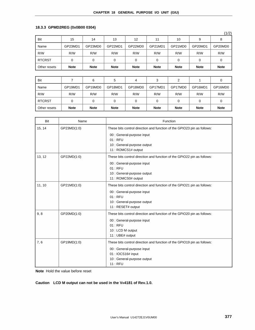
CHAPTER 18 GENERAL PURPOSE I/O UNIT (GIU)
User’s Manual U14272EJ1V0UM00 377
18.3.3 GPMD2REG (0x0B00 0304)
(1/2)
Bit 15 14 13 12 11 10 9 8
Name GP23MD1 GP23MD0 GP22MD1 GP22MD0 GP21MD1 GP21MD0 GP20MD1 GP20MD0
R/W R/W R/W R/W R/W R/W R/W R/W R/W
RTCRST 0 0 0 0 0 0 0 0
Other resets Note Note Note Note Note Note Note Note
Bit 7 6 5 4 3 2 1 0
Name GP19MD1 GP19MD0 GP18MD1 GP18MD0 GP17MD1 GP17MD0 GP16MD1 GP16MD0
R/W R/W R/W R/W R/W R/W R/W R/W R/W
RTCRST 0 0 0 0 0 0 0 0
Other resets Note Note Note Note Note Note Note Note
Bit Name Function
15, 14 GP23MD(1:0) These bits control direction and function of the GPIO23 pin as follows:
00 : General-purpose input
01 : RFU
10 : General-purpose output
11 : ROMCS1# output
13, 12 GP22MD(1:0) These bits control direction and function of the GPIO22 pin as follows:
00 : General-purpose input
01 : RFU
10 : General-purpose output
11 : ROMCS0# output
11, 10 GP21MD(1:0) These bits control direction and function of the GPIO21 pin as follows:
00 : General-purpose input
01 : RFU
10 : General-purpose output
11 : RESET# output
9, 8 GP20MD(1:0) These bits control direction and function of the GPIO20 pin as follows:
00 : General-purpose input
01 : RFU
10 : LCD M output
11 : UBE# output
7, 6 GP19MD(1:0) These bits control direction and function of the GPIO19 pin as follows:
00 : General-purpose input
01 : IOCS16# input
10 : General-purpose output
11 : RFU
Note Hold the value before reset
Caution LCD M output can not be used in the V R4181 of Rev.1.0.
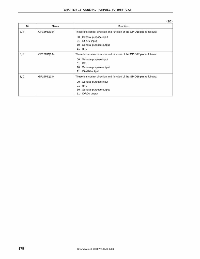
CHAPTER 18 GENERAL PURPOSE I/O UNIT (GIU)
User’s Manual U14272EJ1V0UM00378
(2/2)
Bit Name Function
5, 4 GP18MD(1:0) These bits control direction and function of the GPIO18 pin as follows:
00 : General-purpose input
01 : IORDY input
10 : General-purpose output
11 : RFU
3, 2 GP17MD(1:0) These bits control direction and function of the GPIO17 pin as follows:
00 : General-purpose input
01 : RFU
10 : General-purpose output
11 : IOWR# output
1, 0 GP16MD(1:0) These bits control direction and function of the GPIO16 pin as follows:
00 : General-purpose input
01 : RFU
10 : General-purpose output
11 : IORD# output
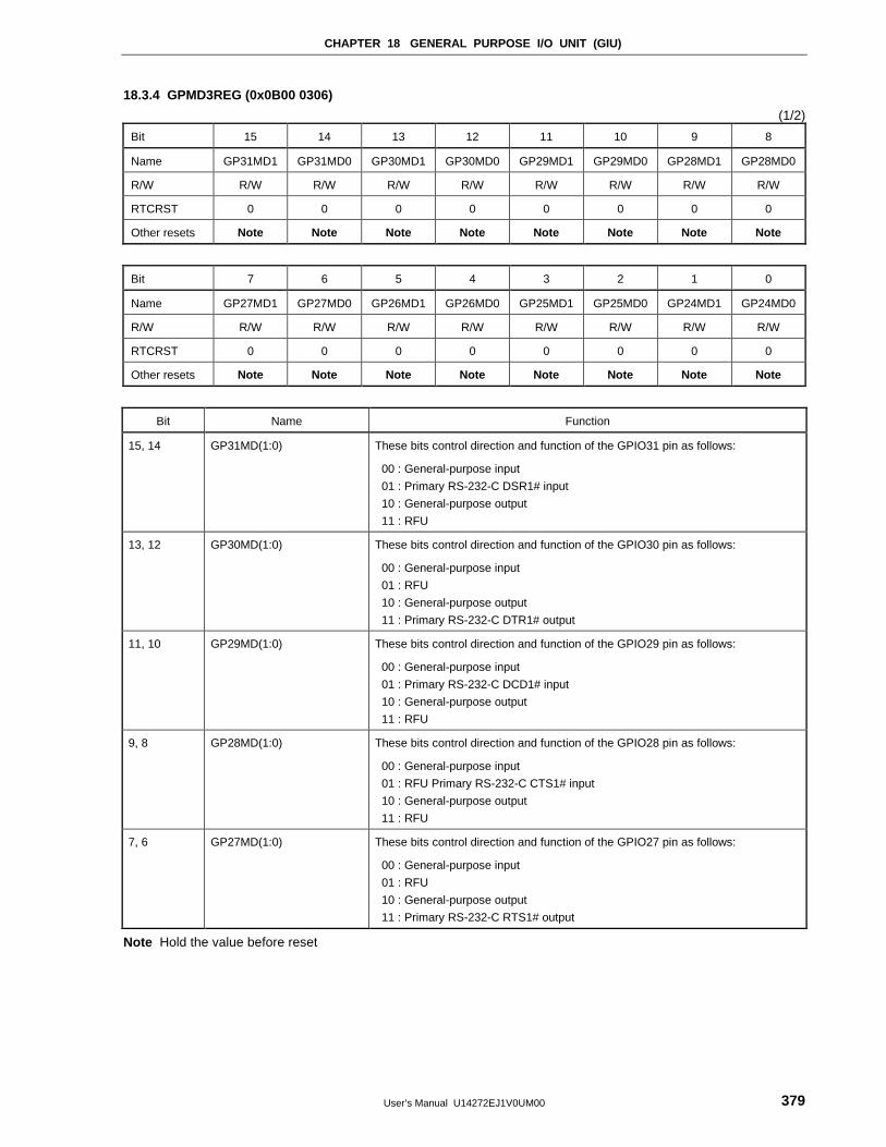
CHAPTER 18 GENERAL PURPOSE I/O UNIT (GIU)
User’s Manual U14272EJ1V0UM00 379
18.3.4 GPMD3REG (0x0B00 0306)
(1/2)
Bit 15 14 13 12 11 10 9 8
Name GP31MD1 GP31MD0 GP30MD1 GP30MD0 GP29MD1 GP29MD0 GP28MD1 GP28MD0
R/W R/W R/W R/W R/W R/W R/W R/W R/W
RTCRST 0 0 0 0 0 0 0 0
Other resets Note Note Note Note Note Note Note Note
Bit 7 6 5 4 3 2 1 0
Name GP27MD1 GP27MD0 GP26MD1 GP26MD0 GP25MD1 GP25MD0 GP24MD1 GP24MD0
R/W R/W R/W R/W R/W R/W R/W R/W R/W
RTCRST 0 0 0 0 0 0 0 0
Other resets Note Note Note Note Note Note Note Note
Bit Name Function
15, 14 GP31MD(1:0) These bits control direction and function of the GPIO31 pin as follows:
00 : General-purpose input
01 : Primary RS-232-C DSR1# input
10 : General-purpose output
11 : RFU
13, 12 GP30MD(1:0) These bits control direction and function of the GPIO30 pin as follows:
00 : General-purpose input
01 : RFU
10 : General-purpose output
11 : Primary RS-232-C DTR1# output
11, 10 GP29MD(1:0) These bits control direction and function of the GPIO29 pin as follows:
00 : General-purpose input
01 : Primary RS-232-C DCD1# input
10 : General-purpose output
11 : RFU
9, 8 GP28MD(1:0) These bits control direction and function of the GPIO28 pin as follows:
00 : General-purpose input
01 : RFU Primary RS-232-C CTS1# input
10 : General-purpose output
11 : RFU
7, 6 GP27MD(1:0) These bits control direction and function of the GPIO27 pin as follows:
00 : General-purpose input
01 : RFU
10 : General-purpose output
11 : Primary RS-232-C RTS1# output
Note Hold the value before reset
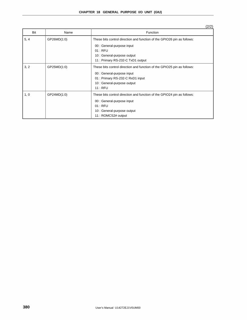
CHAPTER 18 GENERAL PURPOSE I/O UNIT (GIU)
User’s Manual U14272EJ1V0UM00380
(2/2)
Bit Name Function
5, 4 GP26MD(1:0) These bits control direction and function of the GPIO26 pin as follows:
00 : General-purpose input
01 : RFU
10 : General-purpose output
11 : Primary RS-232-C TxD1 output
3, 2 GP25MD(1:0) These bits control direction and function of the GPIO25 pin as follows:
00 : General-purpose input
01 : Primary RS-232-C RxD1 input
10 : General-purpose output
11 : RFU
1, 0 GP24MD(1:0) These bits control direction and function of the GPIO24 pin as follows:
00 : General-purpose input
01 : RFU
10 : General-purpose output
11 : ROMCS2# output
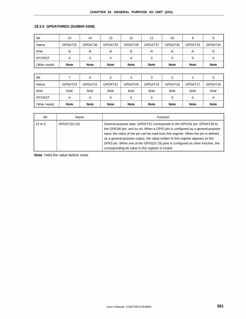
CHAPTER 18 GENERAL PURPOSE I/O UNIT (GIU)
User’s Manual U14272EJ1V0UM00 381
18.3.5 GPDATHREG (0x0B00 0308)
Bit 15 14 13 12 11 10 9 8
Name GPDAT31 GPDAT30 GPDAT29 GPDAT28 GPDAT27 GPDAT26 GPDAT25 GPDAT24
R/W R R R R R R R R
RTCRST 0 0 0 0 0 0 0 0
Other resets Note Note Note Note Note Note Note Note
Bit 7 6 5 4 3 2 1 0
Name GPDAT23 GPDAT22 GPDAT21 GPDAT20 GPDAT19 GPDAT18 GPDAT17 GPDAT16
R/W R/W R/W R/W R/W R/W R/W R/W R/W
RTCRST 0 0 0 0 0 0 0 0
Other resets Note Note Note Note Note Note Note Note
Bit Name Function
15 to 0 GPDAT(31:16) General-purpose data. GPDAT31 corresponds to the GPIO31 pin, GPDAT30 to
the GPIO30 pin, and so on. When a GPIO pin is configured as a general-purpose
input, the value of the pin can be read from this register. When the pin is defined
as a general-purpose output, the value written to this register appears on the
GPIO pin. When one of the GPIO(31:16) pins is configured as other function, the
corresponding bit value in this register is invalid.
Note Hold the value before reset
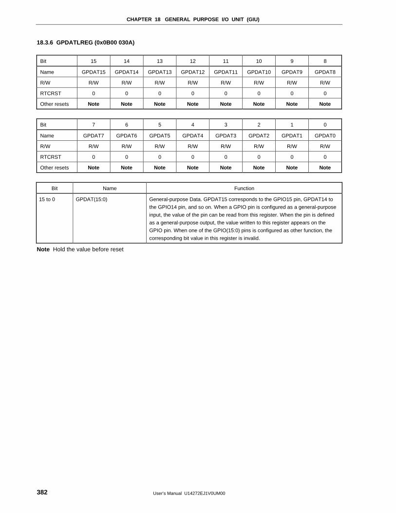
CHAPTER 18 GENERAL PURPOSE I/O UNIT (GIU)
User’s Manual U14272EJ1V0UM00382
18.3.6 GPDATLREG (0x0B00 030A)
Bit 15 14 13 12 11 10 9 8
Name GPDAT15 GPDAT14 GPDAT13 GPDAT12 GPDAT11 GPDAT10 GPDAT9 GPDAT8
R/W R/W R/W R/W R/W R/W R/W R/W R/W
RTCRST 0 0 0 0 0 0 0 0
Other resets Note Note Note Note Note Note Note Note
Bit 7 6 5 4 3 2 1 0
Name GPDAT7 GPDAT6 GPDAT5 GPDAT4 GPDAT3 GPDAT2 GPDAT1 GPDAT0
R/W R/W R/W R/W R/W R/W R/W R/W R/W
RTCRST 0 0 0 0 0 0 0 0
Other resets Note Note Note Note Note Note Note Note
Bit Name Function
15 to 0 GPDAT(15:0) General-purpose Data. GPDAT15 corresponds to the GPIO15 pin, GPDAT14 to
the GPIO14 pin, and so on. When a GPIO pin is configured as a general-purpose
input, the value of the pin can be read from this register. When the pin is defined
as a general-purpose output, the value written to this register appears on the
GPIO pin. When one of the GPIO(15:0) pins is configured as other function, the
corresponding bit value in this register is invalid.
Note Hold the value before reset
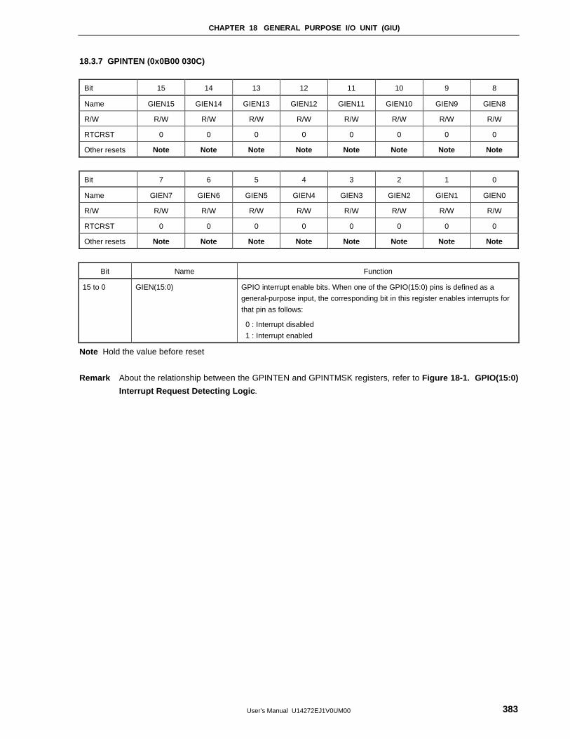
CHAPTER 18 GENERAL PURPOSE I/O UNIT (GIU)
User’s Manual U14272EJ1V0UM00 383
18.3.7 GPINTEN (0x0B00 030C)
Bit 15 14 13 12 11 10 9 8
Name GIEN15 GIEN14 GIEN13 GIEN12 GIEN11 GIEN10 GIEN9 GIEN8
R/W R/W R/W R/W R/W R/W R/W R/W R/W
RTCRST 0 0 0 0 0 0 0 0
Other resets Note Note Note Note Note Note Note Note
Bit 7 6 5 4 3 2 1 0
Name GIEN7 GIEN6 GIEN5 GIEN4 GIEN3 GIEN2 GIEN1 GIEN0
R/W R/W R/W R/W R/W R/W R/W R/W R/W
RTCRST 0 0 0 0 0 0 0 0
Other resets Note Note Note Note Note Note Note Note
Bit Name Function
15 to 0 GIEN(15:0) GPIO interrupt enable bits. When one of the GPIO(15:0) pins is defined as a
general-purpose input, the corresponding bit in this register enables interrupts for
that pin as follows:
0 : Interrupt disabled
1 : Interrupt enabled
Note Hold the value before reset
Remark About the relationship between the GPINTEN and GPINTMSK registers, refer to Figure 18-1. GPIO(15:0)
Interrupt Request Detecting Logic .
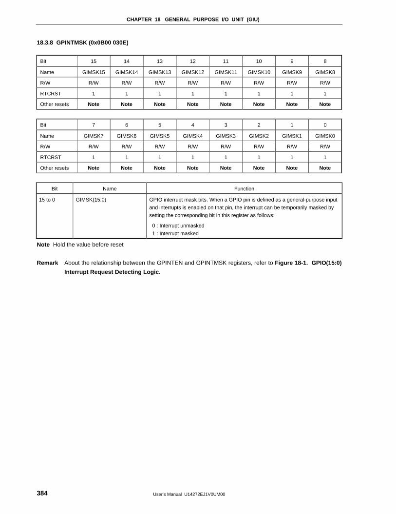
CHAPTER 18 GENERAL PURPOSE I/O UNIT (GIU)
User’s Manual U14272EJ1V0UM00384
18.3.8 GPINTMSK (0x0B00 030E)
Bit 15 14 13 12 11 10 9 8
Name GIMSK15 GIMSK14 GIMSK13 GIMSK12 GIMSK11 GIMSK10 GIMSK9 GIMSK8
R/W R/W R/W R/W R/W R/W R/W R/W R/W
RTCRST 1 1 1 1 1 1 1 1
Other resets Note Note Note Note Note Note Note Note
Bit 7 6 5 4 3 2 1 0
Name GIMSK7 GIMSK6 GIMSK5 GIMSK4 GIMSK3 GIMSK2 GIMSK1 GIMSK0
R/W R/W R/W R/W R/W R/W R/W R/W R/W
RTCRST 1 1 1 1 1 1 1 1
Other resets Note Note Note Note Note Note Note Note
Bit Name Function
15 to 0 GIMSK(15:0) GPIO interrupt mask bits. When a GPIO pin is defined as a general-purpose input
and interrupts is enabled on that pin, the interrupt can be temporarily masked by
setting the corresponding bit in this register as follows:
0 : Interrupt unmasked
1 : Interrupt masked
Note Hold the value before reset
Remark About the relationship between the GPINTEN and GPINTMSK registers, refer to Figure 18-1. GPIO(15:0)
Interrupt Request Detecting Logic .

CHAPTER 18 GENERAL PURPOSE I/O UNIT (GIU)
User’s Manual U14272EJ1V0UM00 385
18.3.9 GPINTTYPH (0x0B00 0310)
(1/2)
Bit 15 14 13 12 11 10 9 8
Name I15TYP1 I15TYP0 I14TYP1 I14TYP0 I13TYP1 I13TYP0 I12TYP1 I12TYP0
R/W R/W R/W R/W R/W R/W R/W R/W R/W
RTCRST 0 0 0 0 0 0 0 0
Other resets Note Note Note Note Note Note Note Note
Bit 7 6 5 4 3 2 1 0
Name I11TYP1 I11TYP0 I10TYP1 I10TYP0 I9TYP1 I9TYP0 I8TYP1 I8TYP0
R/W R/W R/W R/W R/W R/W R/W R/W R/W
RTCRST 0 0 0 0 0 0 0 0
Other resets Note Note Note Note Note Note Note Note
Bit Name Function
15, 14 I15TYP(1:0) These bits define the type of interrupt generated when the GPIO15 pin is defined
as a general-purpose input:
00 : Negative edge triggered interrupt
01 : Positive edge triggered interrupt
10 : Low level triggered interrupt
11 : High level triggered interrupt
13, 12 I14TYP(1:0) These bits define the type of interrupt generated when the GPIO14 pin is defined
as a general-purpose input:
00 : Negative edge triggered interrupt
01 : Positive edge triggered interrupt
10 : Low level triggered interrupt
11 : High level triggered interrupt
11, 10 I13TYP(1:0) These bits define the type of interrupt generated when the GPIO13 pin is defined
as a general-purpose input:
00 : Negative edge triggered interrupt
01 : Positive edge triggered interrupt
10 : Low level triggered interrupt
11 : High level triggered interrupt
9, 8 I12TYP(1:0) These bits define the type of interrupt generated when the GPIO12 pin is defined
as a general-purpose input:
00 : Negative edge triggered interrupt
01 : Positive edge triggered interrupt
10 : Low level triggered interrupt
11 : High level triggered interrupt
Note Hold the value before reset
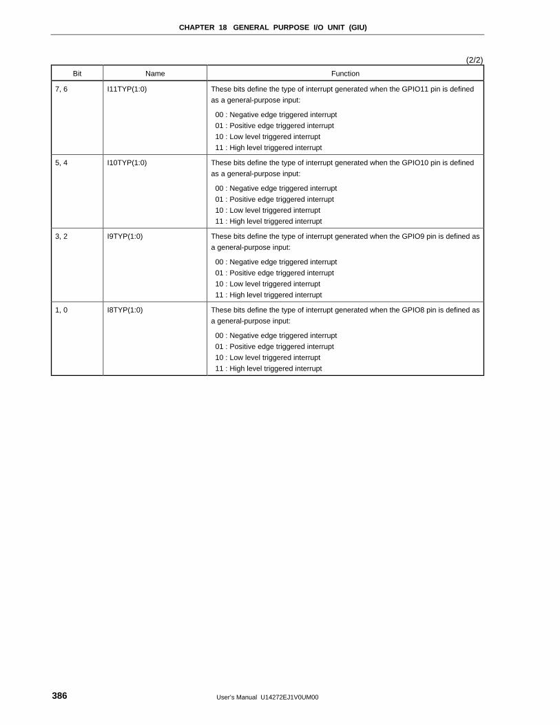
CHAPTER 18 GENERAL PURPOSE I/O UNIT (GIU)
User’s Manual U14272EJ1V0UM00386
(2/2)
Bit Name Function
7, 6 I11TYP(1:0) These bits define the type of interrupt generated when the GPIO11 pin is defined
as a general-purpose input:
00 : Negative edge triggered interrupt
01 : Positive edge triggered interrupt
10 : Low level triggered interrupt
11 : High level triggered interrupt
5, 4 I10TYP(1:0) These bits define the type of interrupt generated when the GPIO10 pin is defined
as a general-purpose input:
00 : Negative edge triggered interrupt
01 : Positive edge triggered interrupt
10 : Low level triggered interrupt
11 : High level triggered interrupt
3, 2 I9TYP(1:0) These bits define the type of interrupt generated when the GPIO9 pin is defined as
a general-purpose input:
00 : Negative edge triggered interrupt
01 : Positive edge triggered interrupt
10 : Low level triggered interrupt
11 : High level triggered interrupt
1, 0 I8TYP(1:0) These bits define the type of interrupt generated when the GPIO8 pin is defined as
a general-purpose input:
00 : Negative edge triggered interrupt
01 : Positive edge triggered interrupt
10 : Low level triggered interrupt
11 : High level triggered interrupt
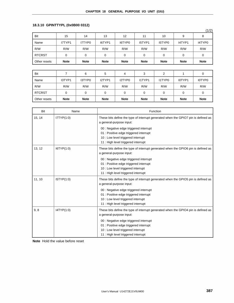
CHAPTER 18 GENERAL PURPOSE I/O UNIT (GIU)
User’s Manual U14272EJ1V0UM00 387
18.3.10 GPINTTYPL (0x0B00 0312)
(1/2)
Bit 15 14 13 12 11 10 9 8
Name I7TYP1 I7TYP0 I6TYP1 I6TYP0 I5TYP1 I5TYP0 I4TYP1 I4TYP0
R/W R/W R/W R/W R/W R/W R/W R/W R/W
RTCRST 0 0 0 0 0 0 0 0
Other resets Note Note Note Note Note Note Note Note
Bit 7 6 5 4 3 2 1 0
Name I3TYP1 I3TYP0 I2TYP1 I2TYP0 I1TYP1 I1TYP0 I0TYP1 I0TYP0
R/W R/W R/W R/W R/W R/W R/W R/W R/W
RTCRST 0 0 0 0 0 0 0 0
Other resets Note Note Note Note Note Note Note Note
Bit Name Function
15, 14 I7TYP(1:0) These bits define the type of interrupt generated when the GPIO7 pin is defined as
a general-purpose input:
00 : Negative edge triggered interrupt
01 : Positive edge triggered interrupt
10 : Low level triggered interrupt
11 : High level triggered interrupt
13, 12 I6TYP(1:0) These bits define the type of interrupt generated when the GPIO6 pin is defined as
a general-purpose input:
00 : Negative edge triggered interrupt
01 : Positive edge triggered interrupt
10 : Low level triggered interrupt
11 : High level triggered interrupt
11, 10 I5TYP(1:0) These bits define the type of interrupt generated when the GPIO5 pin is defined as
a general-purpose input:
00 : Negative edge triggered interrupt
01 : Positive edge triggered interrupt
10 : Low level triggered interrupt
11 : High level triggered interrupt
9, 8 I4TYP(1:0) These bits define the type of interrupt generated when the GPIO4 pin is defined as
a general-purpose input:
00 : Negative edge triggered interrupt
01 : Positive edge triggered interrupt
10 : Low level triggered interrupt
11 : High level triggered interrupt
Note Hold the value before reset
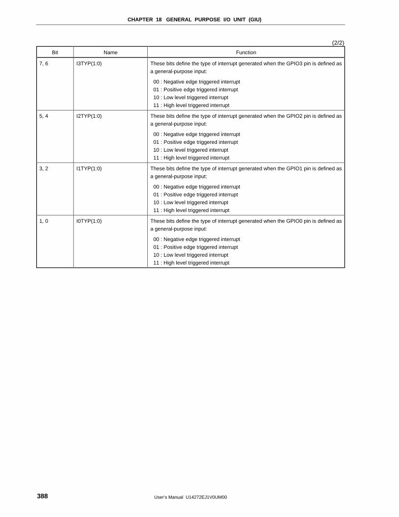
CHAPTER 18 GENERAL PURPOSE I/O UNIT (GIU)
User’s Manual U14272EJ1V0UM00388
(2/2)
Bit Name Function
7, 6 I3TYP(1:0) These bits define the type of interrupt generated when the GPIO3 pin is defined as
a general-purpose input:
00 : Negative edge triggered interrupt
01 : Positive edge triggered interrupt
10 : Low level triggered interrupt
11 : High level triggered interrupt
5, 4 I2TYP(1:0) These bits define the type of interrupt generated when the GPIO2 pin is defined as
a general-purpose input:
00 : Negative edge triggered interrupt
01 : Positive edge triggered interrupt
10 : Low level triggered interrupt
11 : High level triggered interrupt
3, 2 I1TYP(1:0) These bits define the type of interrupt generated when the GPIO1 pin is defined as
a general-purpose input:
00 : Negative edge triggered interrupt
01 : Positive edge triggered interrupt
10 : Low level triggered interrupt
11 : High level triggered interrupt
1, 0 I0TYP(1:0) These bits define the type of interrupt generated when the GPIO0 pin is defined as
a general-purpose input:
00 : Negative edge triggered interrupt
01 : Positive edge triggered interrupt
10 : Low level triggered interrupt
11 : High level triggered interrupt
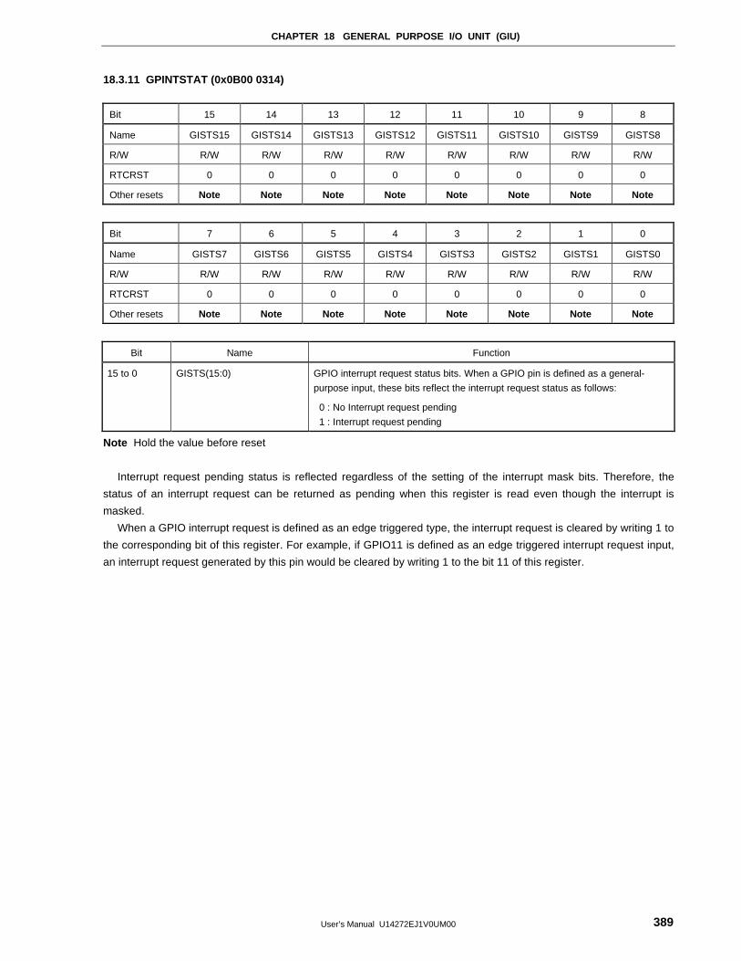
CHAPTER 18 GENERAL PURPOSE I/O UNIT (GIU)
User’s Manual U14272EJ1V0UM00 389
18.3.11 GPINTSTAT (0x0B00 0314)
Bit 15 14 13 12 11 10 9 8
Name GISTS15 GISTS14 GISTS13 GISTS12 GISTS11 GISTS10 GISTS9 GISTS8
R/W R/W R/W R/W R/W R/W R/W R/W R/W
RTCRST 0 0 0 0 0 0 0 0
Other resets Note Note Note Note Note Note Note Note
Bit 7 6 5 4 3 2 1 0
Name GISTS7 GISTS6 GISTS5 GISTS4 GISTS3 GISTS2 GISTS1 GISTS0
R/W R/W R/W R/W R/W R/W R/W R/W R/W
RTCRST 0 0 0 0 0 0 0 0
Other resets Note Note Note Note Note Note Note Note
Bit Name Function
15 to 0 GISTS(15:0) GPIO interrupt request status bits. When a GPIO pin is defined as a general-
purpose input, these bits reflect the interrupt request status as follows:
0 : No Interrupt request pending
1 : Interrupt request pending
Note Hold the value before reset
Interrupt request pending status is reflected regardless of the setting of the interrupt mask bits. Therefore, the
status of an interrupt request can be returned as pending when this register is read even though the interrupt is
masked.
When a GPIO interrupt request is defined as an edge triggered type, the interrupt request is cleared by writing 1 to
the corresponding bit of this register. For example, if GPIO11 is defined as an edge triggered interrupt request input,
an interrupt request generated by this pin would be cleared by writing 1 to the bit 11 of this register.
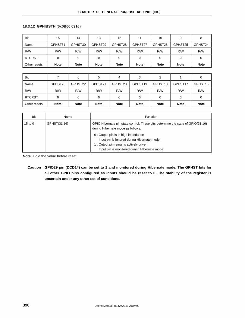
CHAPTER 18 GENERAL PURPOSE I/O UNIT (GIU)
User’s Manual U14272EJ1V0UM00390
18.3.12 GPHIBSTH (0x0B00 0316)
Bit 15 14 13 12 11 10 9 8
Name GPHST31 GPHST30 GPHST29 GPHST28 GPHST27 GPHST26 GPHST25 GPHST24
R/W R/W R/W R/W R/W R/W R/W R/W R/W
RTCRST 0 0 0 0 0 0 0 0
Other resets Note Note Note Note Note Note Note Note
Bit 7 6 5 4 3 2 1 0
Name GPHST23 GPHST22 GPHST21 GPHST20 GPHST19 GPHST18 GPHST17 GPHST16
R/W R/W R/W R/W R/W R/W R/W R/W R/W
RTCRST 0 0 0 0 0 0 0 0
Other resets Note Note Note Note Note Note Note Note
Bit Name Function
15 to 0 GPHST(31:16) GPIO Hibernate pin state control. These bits determine the state of GPIO(31:16)
during Hibernate mode as follows:
0 : Output pin is in high impedance
Input pin is ignored during Hibernate mode
1 : Output pin remains actively driven
Input pin is monitored during Hibernate mode
Note Hold the value before reset
Caution GPIO29 pin (DCD1#) can be set to 1 and monitored during Hibernate mode. The GPHST bits for
all other GPIO pins configured as inputs should be reset to 0. The stability of the register is
uncertain under any other set of conditions.
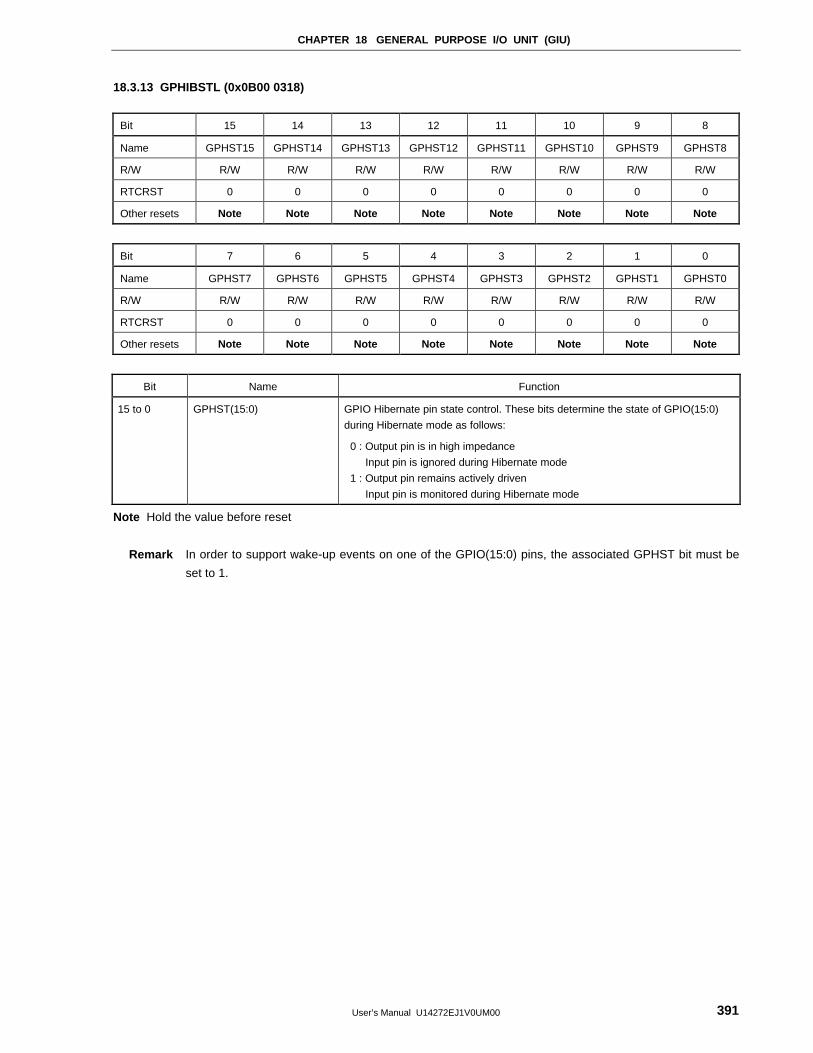
CHAPTER 18 GENERAL PURPOSE I/O UNIT (GIU)
User’s Manual U14272EJ1V0UM00 391
18.3.13 GPHIBSTL (0x0B00 0318)
Bit 15 14 13 12 11 10 9 8
Name GPHST15 GPHST14 GPHST13 GPHST12 GPHST11 GPHST10 GPHST9 GPHST8
R/W R/W R/W R/W R/W R/W R/W R/W R/W
RTCRST 0 0 0 0 0 0 0 0
Other resets Note Note Note Note Note Note Note Note
Bit 7 6 5 4 3 2 1 0
Name GPHST7 GPHST6 GPHST5 GPHST4 GPHST3 GPHST2 GPHST1 GPHST0
R/W R/W R/W R/W R/W R/W R/W R/W R/W
RTCRST 0 0 0 0 0 0 0 0
Other resets Note Note Note Note Note Note Note Note
Bit Name Function
15 to 0 GPHST(15:0) GPIO Hibernate pin state control. These bits determine the state of GPIO(15:0)
during Hibernate mode as follows:
0 : Output pin is in high impedance
Input pin is ignored during Hibernate mode
1 : Output pin remains actively driven
Input pin is monitored during Hibernate mode
Note Hold the value before reset
Remark In order to support wake-up events on one of the GPIO(15:0) pins, the associated GPHST bit must be
set to 1.
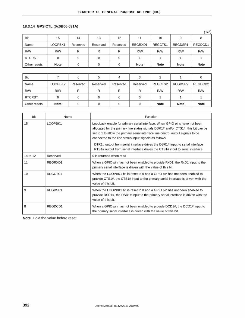
CHAPTER 18 GENERAL PURPOSE I/O UNIT (GIU)
User’s Manual U14272EJ1V0UM00392
18.3.14 GPSICTL (0x0B00 031A)
(1/2)
Bit 15 14 13 12 11 10 9 8
Name LOOPBK1 Reserved Reserved Reserved REGRXD1 REGCTS1 REGDSR1 REGDCD1
R/W R/W R R R R/W R/W R/W R/W
RTCRST 0 0 0 0 1 1 1 1
Other resets Note 0 0 0 Note Note Note Note
Bit 7 6 5 4 3 2 1 0
Name LOOPBK2 Reserved Reserved Reserved Reserved REGCTS2 REGDSR2 REGDCD2
R/W R/W R R R R R/W R/W R/W
RTCRST 0 0 0 0 0 1 1 1
Other resets Note 0 0 0 0 Note Note Note
Bit Name Function
15 LOOPBK1 Loopback enable for primary serial interface. When GPIO pins have not been
allocated for the primary line status signals DSR1# and/or CTS1#, this bit can be
set to 1 to allow the primary serial interface line control output signals to be
connected to the line status input signals as follows:
DTR1# output from serial interface drives the DSR1# input to serial interface
RTS1# output from serial interface drives the CTS1# input to serial interface
14 to 12 Reserved 0 is returned when read
11 REGRXD1 When a GPIO pin has not been enabled to provide RxD1, the RxD1 input to the
primary serial interface is driven with the value of this bit.
10 REGCTS1 When the LOOPBK1 bit is reset to 0 and a GPIO pin has not been enabled to
provide CTS1#, the CTS1# input to the primary serial interface is driven with the
value of this bit.
9 REGDSR1 When the LOOPBK1 bit is reset to 0 and a GPIO pin has not been enabled to
provide DSR1#, the DSR1# input to the primary serial interface is driven with the
value of this bit.
8 REGDCD1 When a GPIO pin has not been enabled to provide DCD1#, the DCD1# input to
the primary serial interface is driven with the value of this bit.
Note Hold the value before reset
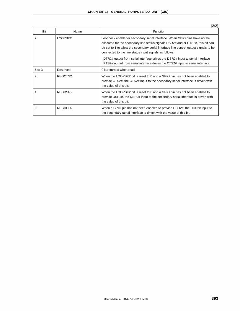
CHAPTER 18 GENERAL PURPOSE I/O UNIT (GIU)
User’s Manual U14272EJ1V0UM00 393
(2/2)
Bit Name Function
7 LOOPBK2 Loopback enable for secondary serial interface. When GPIO pins have not be
allocated for the secondary line status signals DSR2# and/or CTS2#, this bit can
be set to 1 to allow the secondary serial interface line control output signals to be
connected to the line status input signals as follows:
DTR2# output from serial interface drives the DSR2# input to serial interface
RTS2# output from serial interface drives the CTS2# input to serial interface
6 to 3 Reserved 0 is returned when read
2 REGCTS2 When the LOOPBK2 bit is reset to 0 and a GPIO pin has not been enabled to
provide CTS2#, the CTS2# input to the secondary serial interface is driven with
the value of this bit.
1 REGDSR2 When the LOOPBK2 bit is reset to 0 and a GPIO pin has not been enabled to
provide DSR2#, the DSR2# input to the secondary serial interface is driven with
the value of this bit.
0 REGDCD2 When a GPIO pin has not been enabled to provide DCD2#, the DCD2# input to
the secondary serial interface is driven with the value of this bit.
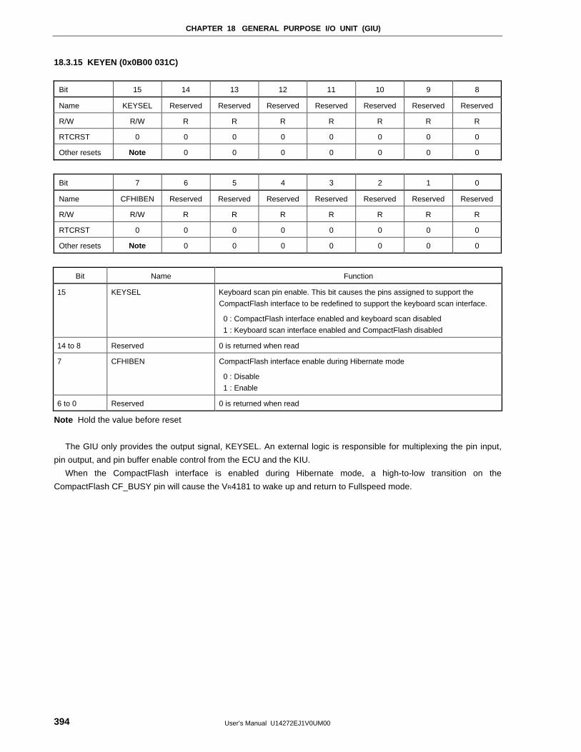
CHAPTER 18 GENERAL PURPOSE I/O UNIT (GIU)
User’s Manual U14272EJ1V0UM00394
18.3.15 KEYEN (0x0B00 031C)
Bit 15 14 13 12 11 10 9 8
Name KEYSEL Reserved Reserved Reserved Reserved Reserved Reserved Reserved
R/W R/W R R R R R R R
RTCRST 0 0 0 0 0 0 0 0
Other resets Note 0 0 0 0 0 0 0
Bit 7 6 5 4 3 2 1 0
Name CFHIBEN Reserved Reserved Reserved Reserved Reserved Reserved Reserved
R/W R/W R R R R R R R
RTCRST 0 0 0 0 0 0 0 0
Other resets Note 0 0 0 0 0 0 0
Bit Name Function
15 KEYSEL Keyboard scan pin enable. This bit causes the pins assigned to support the
CompactFlash interface to be redefined to support the keyboard scan interface.
0 : CompactFlash interface enabled and keyboard scan disabled
1 : Keyboard scan interface enabled and CompactFlash disabled
14 to 8 Reserved 0 is returned when read
7 CFHIBEN CompactFlash interface enable during Hibernate mode
0 : Disable
1 : Enable
6 to 0 Reserved 0 is returned when read
Note Hold the value before reset
The GIU only provides the output signal, KEYSEL. An external logic is responsible for multiplexing the pin input,
pin output, and pin buffer enable control from the ECU and the KIU.
When the CompactFlash interface is enabled during Hibernate mode, a high-to-low transition on the
CompactFlash CF_BUSY pin will cause the VR4181 to wake up and return to Fullspeed mode.
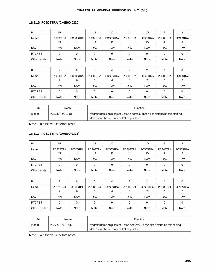
CHAPTER 18 GENERAL PURPOSE I/O UNIT (GIU)
User’s Manual U14272EJ1V0UM00 395
18.3.16 PCS0STRA (0x0B00 0320)
Bit 15 14 13 12 11 10 9 8
Name PCS0STRA
15
PCS0STRA
14
PCS0STRA
13
PCS0STRA
12
PCS0STRA
11
PCS0STRA
10
PCS0STRA
9
PCS0STRA
8
R/W R/W R/W R/W R/W R/W R/W R/W R/W
RTCRST 0 0 0 0 0 0 0 0
Other resets Note Note Note Note Note Note Note Note
Bit 7 6 5 4 3 2 1 0
Name PCS0STRA
7
PCS0STRA
6
PCS0STRA
5
PCS0STRA
4
PCS0STRA
3
PCS0STRA
2
PCS0STRA
1
PCS0STRA
0
R/W R/W R/W R/W R/W R/W R/W R/W R/W
RTCRST 0 0 0 0 0 0 0 0
Other resets Note Note Note Note Note Note Note Note
Bit Name Function
15 to 0 PCS0STRA(15:0) Programmable chip select 0 start address. These bits determine the starting
address for the memory or I/O chip select.
Note Hold the value before reset
18.3.17 PCS0STPA (0x0B00 0322)
Bit 15 14 13 12 11 10 9 8
Name PCS0STPA
15
PCS0STPA
14
PCS0STPA
13
PCS0STPA
12
PCS0STPA
11
PCS0STPA
10
PCS0STPA
9
PCS0STPA
8
R/W R/W R/W R/W R/W R/W R/W R/W R/W
RTCRST 0 0 0 0 0 0 0 0
Other resets Note Note Note Note Note Note Note Note
Bit 7 6 5 4 3 2 1 0
Name PCS0STPA
7
PCS0STPA
6
PCS0STPA
5
PCS0STPA
4
PCS0STPA
3
PCS0STPA
2
PCS0STPA
1
PCS0STPA
0
R/W R/W R/W R/W R/W R/W R/W R/W R/W
RTCRST 0 0 0 0 0 0 0 0
Other resets Note Note Note Note Note Note Note Note
Bit Name Function
15 to 0 PCS0STPA(15:0) Programmable chip select 0 stop address. These bits determine the ending
address for the memory or I/O chip select.
Note Hold the value before reset
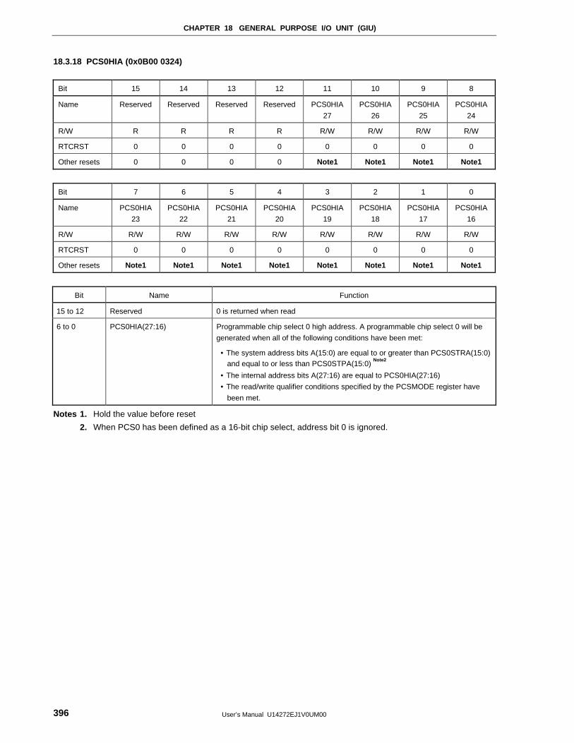
CHAPTER 18 GENERAL PURPOSE I/O UNIT (GIU)
User’s Manual U14272EJ1V0UM00396
18.3.18 PCS0HIA (0x0B00 0324)
Bit 15 14 13 12 11 10 9 8
Name Reserved Reserved Reserved Reserved PCS0HIA
27
PCS0HIA
26
PCS0HIA
25
PCS0HIA
24
R/W R R R R R/W R/W R/W R/W
RTCRST 0 0 0 0 0 0 0 0
Other resets 0 0 0 0 Note1 Note1 Note1 Note1
Bit 7 6 5 4 3 2 1 0
Name PCS0HIA
23
PCS0HIA
22
PCS0HIA
21
PCS0HIA
20
PCS0HIA
19
PCS0HIA
18
PCS0HIA
17
PCS0HIA
16
R/W R/W R/W R/W R/W R/W R/W R/W R/W
RTCRST 0 0 0 0 0 0 0 0
Other resets Note1 Note1 Note1 Note1 Note1 Note1 Note1 Note1
Bit Name Function
15 to 12 Reserved 0 is returned when read
6 to 0 PCS0HIA(27:16) Programmable chip select 0 high address. A programmable chip select 0 will be
generated when all of the following conditions have been met:
• The system address bits A(15:0) are equal to or greater than PCS0STRA(15:0) and equal to or less than PCS0STPA(15:0)
Note2
• The internal address bits A(27:16) are equal to PCS0HIA(27:16)
• The read/write qualifier conditions specified by the PCSMODE register have
been met.
Notes 1. Hold the value before reset
2. When PCS0 has been defined as a 16-bit chip select, address bit 0 is ignored.
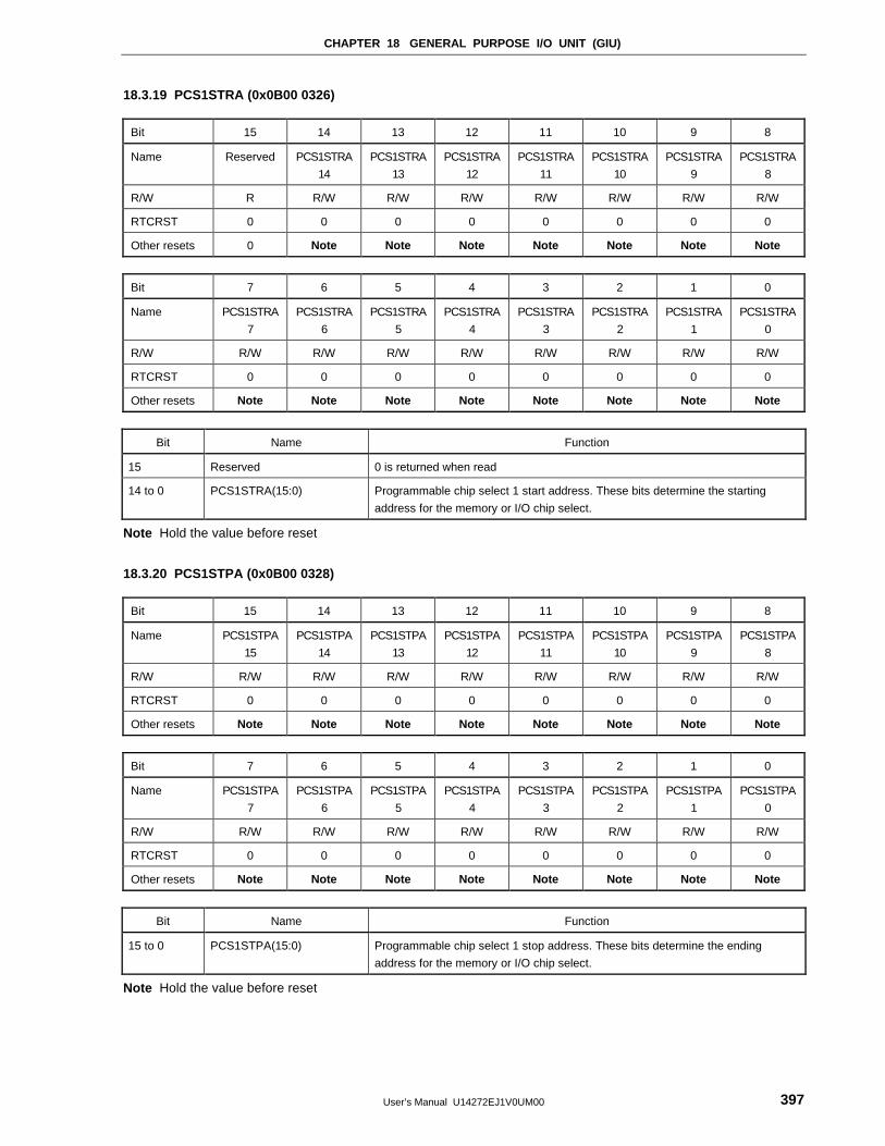
CHAPTER 18 GENERAL PURPOSE I/O UNIT (GIU)
User’s Manual U14272EJ1V0UM00 397
18.3.19 PCS1STRA (0x0B00 0326)
Bit 15 14 13 12 11 10 9 8
Name Reserved PCS1STRA
14
PCS1STRA
13
PCS1STRA
12
PCS1STRA
11
PCS1STRA
10
PCS1STRA
9
PCS1STRA
8
R/W R R/W R/W R/W R/W R/W R/W R/W
RTCRST 0 0 0 0 0 0 0 0
Other resets 0 Note Note Note Note Note Note Note
Bit 7 6 5 4 3 2 1 0
Name PCS1STRA
7
PCS1STRA
6
PCS1STRA
5
PCS1STRA
4
PCS1STRA
3
PCS1STRA
2
PCS1STRA
1
PCS1STRA
0
R/W R/W R/W R/W R/W R/W R/W R/W R/W
RTCRST 0 0 0 0 0 0 0 0
Other resets Note Note Note Note Note Note Note Note
Bit Name Function
15 Reserved 0 is returned when read
14 to 0 PCS1STRA(15:0) Programmable chip select 1 start address. These bits determine the starting
address for the memory or I/O chip select.
Note Hold the value before reset
18.3.20 PCS1STPA (0x0B00 0328)
Bit 15 14 13 12 11 10 9 8
Name PCS1STPA
15
PCS1STPA
14
PCS1STPA
13
PCS1STPA
12
PCS1STPA
11
PCS1STPA
10
PCS1STPA
9
PCS1STPA
8
R/W R/W R/W R/W R/W R/W R/W R/W R/W
RTCRST 0 0 0 0 0 0 0 0
Other resets Note Note Note Note Note Note Note Note
Bit 7 6 5 4 3 2 1 0
Name PCS1STPA
7
PCS1STPA
6
PCS1STPA
5
PCS1STPA
4
PCS1STPA
3
PCS1STPA
2
PCS1STPA
1
PCS1STPA
0
R/W R/W R/W R/W R/W R/W R/W R/W R/W
RTCRST 0 0 0 0 0 0 0 0
Other resets Note Note Note Note Note Note Note Note
Bit Name Function
15 to 0 PCS1STPA(15:0) Programmable chip select 1 stop address. These bits determine the ending
address for the memory or I/O chip select.
Note Hold the value before reset

CHAPTER 18 GENERAL PURPOSE I/O UNIT (GIU)
User’s Manual U14272EJ1V0UM00398
18.3.21 PCS1HIA (0x0B00 032A)
Bit 15 14 13 12 11 10 9 8
Name Reserved Reserved Reserved Reserved PCS1HIA
27
PCS1HIA
26
PCS1HIA
25
PCS1HIA
24
R/W R R R R R/W R/W R/W R/W
RTCRST 0 0 0 0 0 0 0 0
Other resets 0 0 0 0 Note1 Note1 Note1 Note1
Bit 7 6 5 4 3 2 1 0
Name PCS1HIA
23
PCS1HIA
22
PCS1HIA
21
PCS1HIA
20
PCS1HIA
19
PCS1HIA
18
PCS1HIA
17
PCS1HIA
16
R/W R/W R/W R/W R/W R/W R/W R/W R/W
RTCRST 0 0 0 0 0 0 0 0
Other resets Note1 Note1 Note1 Note1 Note1 Note1 Note1 Note1
Bit Name Function
15 to 12 Reserved 0 is returned when read
11 to 0 PCS1HIA(27:16) Programmable chip select 1 high address. A programmable chip select 1 will be
generated when all of the following conditions have been met:
• The system address bits A(15:0) are equal to or greater than PCS1STRA(15:0) and equal to or less than PCS1STPA(15:0)
Note2
• The internal address bits A(27:16) are equal to PCS1HIA(27:16)
• The read/write qualifier conditions specified by the PCSMODE register have
been met.
Notes 1. Hold the value before reset
2. When PCS1 has been defined as a 16-bit chip select, address bit 0 is ignored.
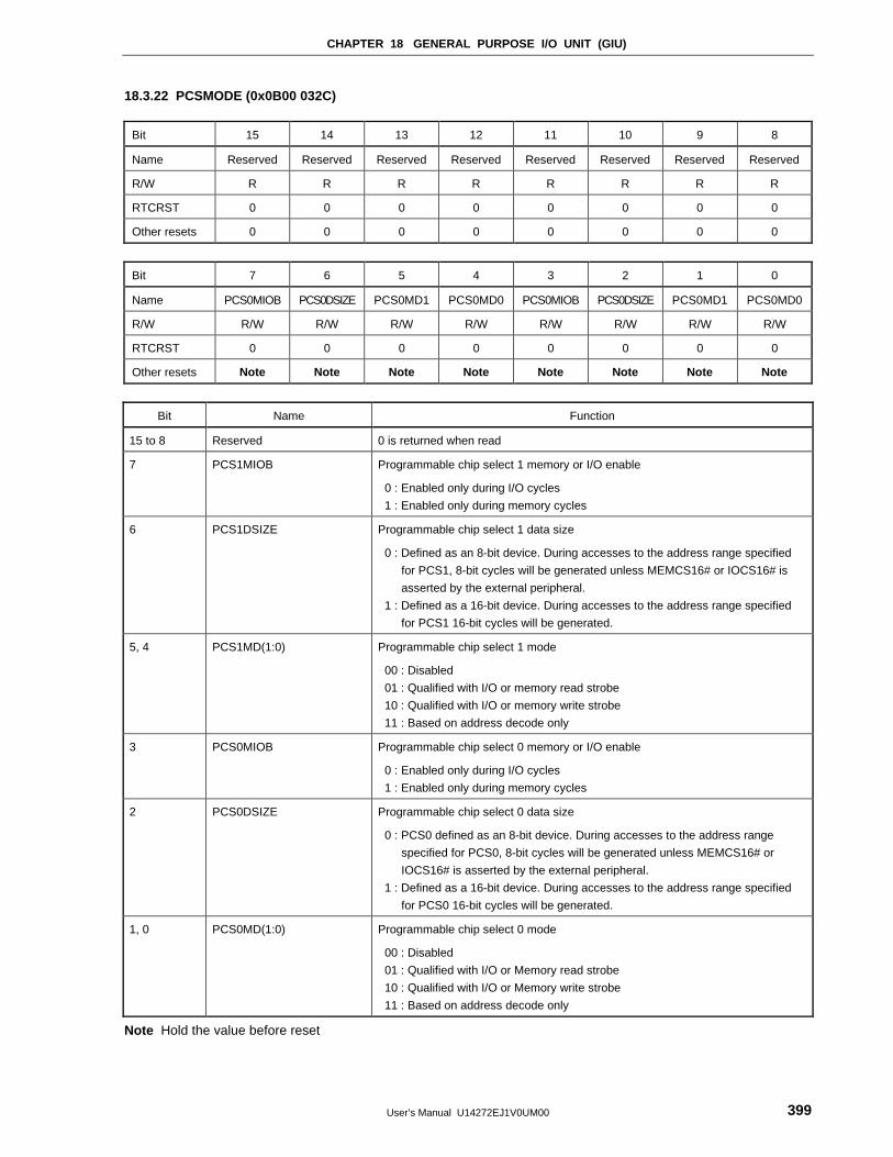
CHAPTER 18 GENERAL PURPOSE I/O UNIT (GIU)
User’s Manual U14272EJ1V0UM00 399
18.3.22 PCSMODE (0x0B00 032C)
Bit 15 14 13 12 11 10 9 8
Name Reserved Reserved Reserved Reserved Reserved Reserved Reserved Reserved
R/W R R R R R R R R
RTCRST 0 0 0 0 0 0 0 0
Other resets 0 0 0 0 0 0 0 0
Bit 7 6 5 4 3 2 1 0
Name PCS0MIOB PCS0DSIZE PCS0MD1 PCS0MD0 PCS0MIOB PCS0DSIZE PCS0MD1 PCS0MD0
R/W R/W R/W R/W R/W R/W R/W R/W R/W
RTCRST 0 0 0 0 0 0 0 0
Other resets Note Note Note Note Note Note Note Note
Bit Name Function
15 to 8 Reserved 0 is returned when read
7 PCS1MIOB Programmable chip select 1 memory or I/O enable
0 : Enabled only during I/O cycles
1 : Enabled only during memory cycles
6 PCS1DSIZE Programmable chip select 1 data size
0 : Defined as an 8-bit device. During accesses to the address range specified
for PCS1, 8-bit cycles will be generated unless MEMCS16# or IOCS16# is
asserted by the external peripheral.
1 : Defined as a 16-bit device. During accesses to the address range specified
for PCS1 16-bit cycles will be generated.
5, 4 PCS1MD(1:0) Programmable chip select 1 mode
00 : Disabled
01 : Qualified with I/O or memory read strobe
10 : Qualified with I/O or memory write strobe
11 : Based on address decode only
3 PCS0MIOB Programmable chip select 0 memory or I/O enable
0 : Enabled only during I/O cycles
1 : Enabled only during memory cycles
2 PCS0DSIZE Programmable chip select 0 data size
0 : PCS0 defined as an 8-bit device. During accesses to the address range
specified for PCS0, 8-bit cycles will be generated unless MEMCS16# or
IOCS16# is asserted by the external peripheral.
1 : Defined as a 16-bit device. During accesses to the address range specified
for PCS0 16-bit cycles will be generated.
1, 0 PCS0MD(1:0) Programmable chip select 0 mode
00 : Disabled
01 : Qualified with I/O or Memory read strobe
10 : Qualified with I/O or Memory write strobe
11 : Based on address decode only
Note Hold the value before reset
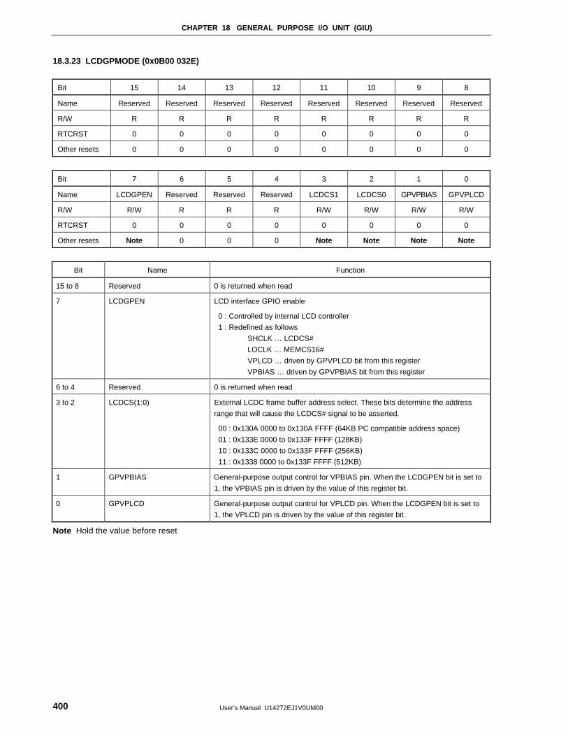
CHAPTER 18 GENERAL PURPOSE I/O UNIT (GIU)
User’s Manual U14272EJ1V0UM00400
18.3.23 LCDGPMODE (0x0B00 032E)
Bit 15 14 13 12 11 10 9 8
Name Reserved Reserved Reserved Reserved Reserved Reserved Reserved Reserved
R/W R R R R R R R R
RTCRST 0 0 0 0 0 0 0 0
Other resets 0 0 0 0 0 0 0 0
Bit 7 6 5 4 3 2 1 0
Name LCDGPEN Reserved Reserved Reserved LCDCS1 LCDCS0 GPVPBIAS GPVPLCD
R/W R/W R R R R/W R/W R/W R/W
RTCRST 0 0 0 0 0 0 0 0
Other resets Note 0 0 0 Note Note Note Note
Bit Name Function
15 to 8 Reserved 0 is returned when read
7 LCDGPEN LCD interface GPIO enable
0 : Controlled by internal LCD controller
1 : Redefined as follows
SHCLK … LCDCS#
LOCLK … MEMCS16#
VPLCD … driven by GPVPLCD bit from this register
VPBIAS … driven by GPVPBIAS bit from this register
6 to 4 Reserved 0 is returned when read
3 to 2 LCDCS(1:0) External LCDC frame buffer address select. These bits determine the address
range that will cause the LCDCS# signal to be asserted.
00 : 0x130A 0000 to 0x130A FFFF (64KB PC compatible address space)
01 : 0x133E 0000 to 0x133F FFFF (128KB)
10 : 0x133C 0000 to 0x133F FFFF (256KB)
11 : 0x1338 0000 to 0x133F FFFF (512KB)
1 GPVPBIAS General-purpose output control for VPBIAS pin. When the LCDGPEN bit is set to
1, the VPBIAS pin is driven by the value of this register bit.
0 GPVPLCD General-purpose output control for VPLCD pin. When the LCDGPEN bit is set to
1, the VPLCD pin is driven by the value of this register bit.
Note Hold the value before reset
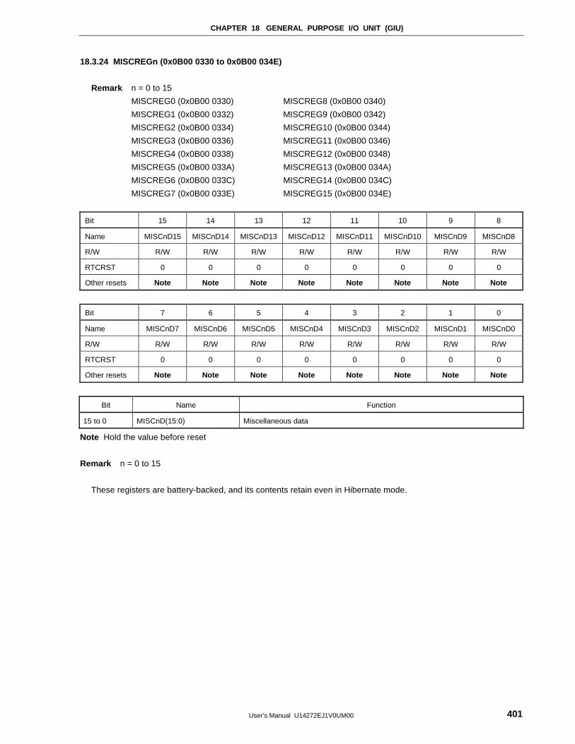
CHAPTER 18 GENERAL PURPOSE I/O UNIT (GIU)
User’s Manual U14272EJ1V0UM00 401
18.3.24 MISCREGn (0x0B00 0330 to 0x0B00 034E)
Remark n = 0 to 15
MISCREG0 (0x0B00 0330) MISCREG8 (0x0B00 0340)
MISCREG1 (0x0B00 0332) MISCREG9 (0x0B00 0342)
MISCREG2 (0x0B00 0334) MISCREG10 (0x0B00 0344)
MISCREG3 (0x0B00 0336) MISCREG11 (0x0B00 0346)
MISCREG4 (0x0B00 0338) MISCREG12 (0x0B00 0348)
MISCREG5 (0x0B00 033A) MISCREG13 (0x0B00 034A)
MISCREG6 (0x0B00 033C) MISCREG14 (0x0B00 034C)
MISCREG7 (0x0B00 033E) MISCREG15 (0x0B00 034E)
Bit 15 14 13 12 11 10 9 8
Name MISCnD15 MISCnD14 MISCnD13 MISCnD12 MISCnD11 MISCnD10 MISCnD9 MISCnD8
R/W R/W R/W R/W R/W R/W R/W R/W R/W
RTCRST 0 0 0 0 0 0 0 0
Other resets Note Note Note Note Note Note Note Note
Bit 7 6 5 4 3 2 1 0
Name MISCnD7 MISCnD6 MISCnD5 MISCnD4 MISCnD3 MISCnD2 MISCnD1 MISCnD0
R/W R/W R/W R/W R/W R/W R/W R/W R/W
RTCRST 0 0 0 0 0 0 0 0
Other resets Note Note Note Note Note Note Note Note
Bit Name Function
15 to 0 MISCnD(15:0) Miscellaneous data
Note Hold the value before reset
Remark n = 0 to 15
These registers are battery-backed, and its contents retain even in Hibernate mode.

User’s Manual U14272EJ1V0UM00402
[MEMO]
User’s Manual U14272EJ1V0UM00 403
CHAPTER 19 TOUCH PANEL INTERFACE UNIT (PIU)
This chapter describes the PIU’s operations and register settings.
19.1 General
The PIU uses an on-chip A/D converter and detects the X and Y coordinates of pen contact locations on the touch
panel and scans the general-purpose A/D input port. Since the touch panel control circuit and the A/D converter
(conversion precision: 10 bits) are both on-chip, the touch panel is connected directly to the VR4181.
The PIU’s function, namely the detection of X and Y coordinates, is performed partly by hardware and partly by
software.
Hardware tasks : • Touch panel applied voltage control
• Reception of coordinate data
Software task : • Processing of coordinate data based on data sampled by hardware
Features of the PIU’s hardware tasks are described below.
• Can be directly connected to touch panel with four-pin resistance layers (on-chip touch panel driver)
• Interface for on-chip A/D converter
• Voltage detection at three general-purpose AD ports and one audio input port
• Operation of A/D converter based on various settings and control of voltage applied to touch panel
• Sampling of X-coordinate and Y-coordinate data
• Variable coordinate data sampling interval
• Interrupt is triggered if pen touch occurs regardless of CPU operation mode (interrupts do not occur when in
CPU hibernate mode)
• Four dedicated buffers for up to two pages each of coordinate data
• Four buffers for A/D port scan
• Auto/manual options for coordinate data sampling start/stop control
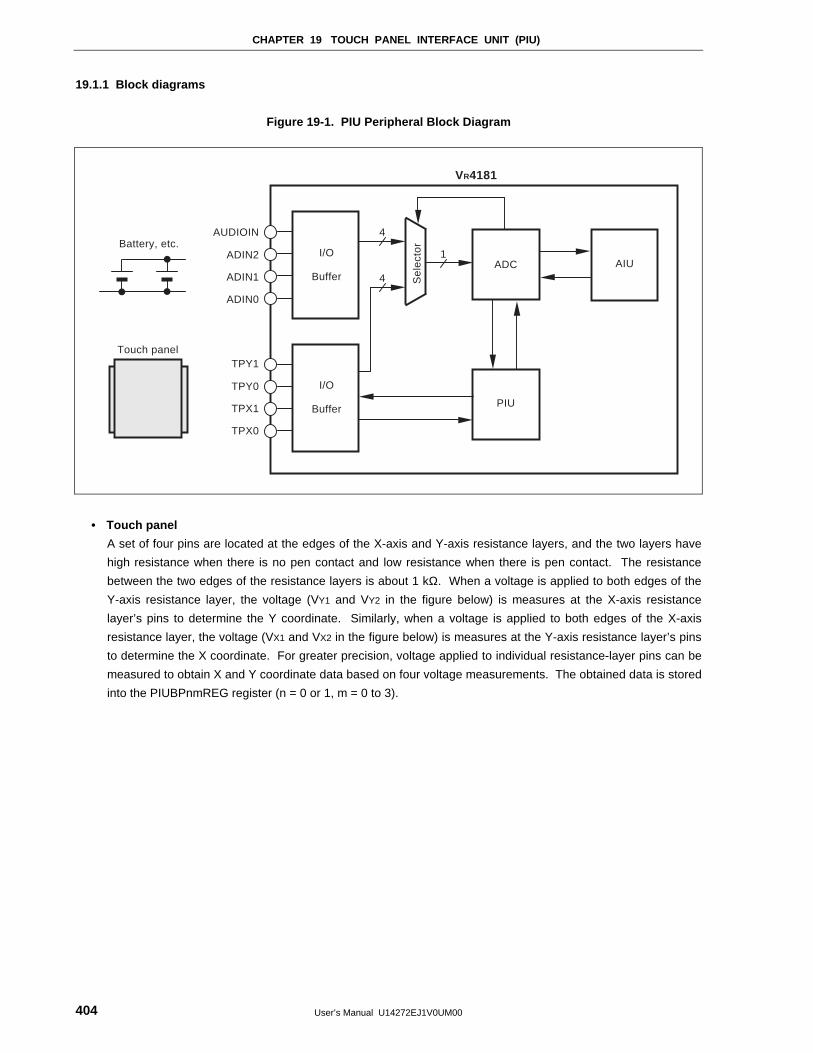
CHAPTER 19 TOUCH PANEL INTERFACE UNIT (PIU)
User’s Manual U14272EJ1V0UM00404
19.1.1 Block diagrams
Figure 19-1. PIU Peripheral Block Diagram
VR4181
Battery, etc.I/O
Buffer
I/O
Buffer PIU
ADC
Se
lect
or
4
AIU
AUDIOIN
ADIN2
ADIN1
ADIN0
TPY1
TPY0
TPX1
TPX0
Touch panel
4
1
• Touch panel
A set of four pins are located at the edges of the X-axis and Y-axis resistance layers, and the two layers have
high resistance when there is no pen contact and low resistance when there is pen contact. The resistance
between the two edges of the resistance layers is about 1 kΩ. When a voltage is applied to both edges of the
Y-axis resistance layer, the voltage (VY1 and VY2 in the figure below) is measures at the X-axis resistance
layer’s pins to determine the Y coordinate. Similarly, when a voltage is applied to both edges of the X-axis
resistance layer, the voltage (VX1 and VX2 in the figure below) is measures at the Y-axis resistance layer’s pins
to determine the X coordinate. For greater precision, voltage applied to individual resistance-layer pins can be
measured to obtain X and Y coordinate data based on four voltage measurements. The obtained data is stored
into the PIUBPnmREG register (n = 0 or 1, m = 0 to 3).
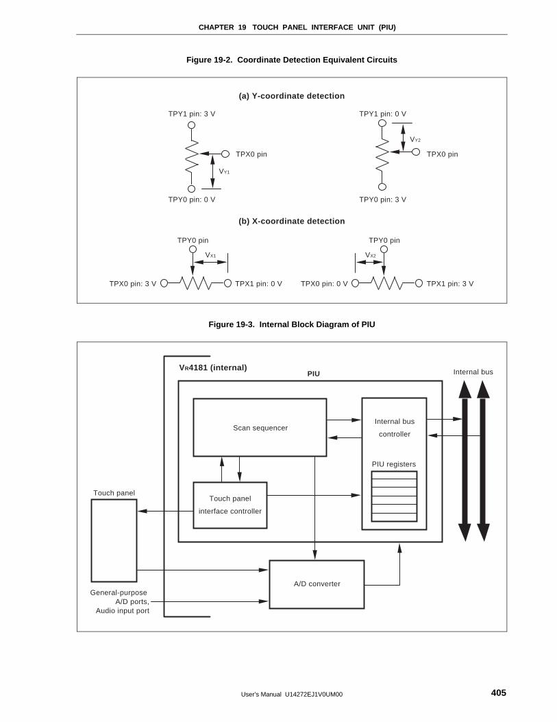
CHAPTER 19 TOUCH PANEL INTERFACE UNIT (PIU)
User’s Manual U14272EJ1V0UM00 405
Figure 19-2. Coordinate Detection Equivalent Circuits
TPX0 pin
TPX1 pin: 0 VTPX0 pin: 3 V
VY1
VX1
TPY1 pin: 3 V
(a) Y-coordinate detection
(b) X-coordinate detection
TPY0 pin: 0 V
TPY0 pin
TPX1 pin: 3 VTPX0 pin: 0 V
VX2
TPY0 pin
TPX0 pin
VY2
TPY1 pin: 0 V
TPY0 pin: 3 V
Figure 19-3. Internal Block Diagram of PIU
VR4181 (internal)
Scan sequencer
Touch panel
interface controller
A/D converterGeneral-purpose
A/D ports,Audio input port
PIU
PIU registers
Internal bus
controller
Internal bus
Touch panel
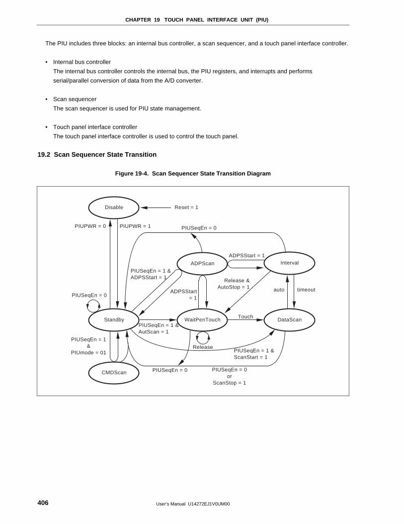
CHAPTER 19 TOUCH PANEL INTERFACE UNIT (PIU)
User’s Manual U14272EJ1V0UM00406
The PIU includes three blocks: an internal bus controller, a scan sequencer, and a touch panel interface controller.
• Internal bus controller
The internal bus controller controls the internal bus, the PIU registers, and interrupts and performs
serial/parallel conversion of data from the A/D converter.
• Scan sequencer
The scan sequencer is used for PIU state management.
• Touch panel interface controller
The touch panel interface controller is used to control the touch panel.
19.2 Scan Sequencer State Transition
Figure 19-4. Scan Sequencer State Transition Diagram
Disable Reset = 1
PIUPWR = 1
PIUSeqEn = 1 &ADPSStart = 1
PIUSeqEn = 1 &AutScan = 1
Release &AutoStop = 1
PIUPWR = 0
ADPSStart = 1
timeout
PIUSeqEn = 1 &ScanStart = 1
PIUSeqEn = 0or
ScanStop = 1
auto
Standby
PIUSeqEn = 1&
PIUmode = 01
PIUSeqEn = 0
WaitPenTouch
ADPScan
ADPSStart = 1
Touch
PIUSeqEn = 0
DataScan
Interval
CMDScan
Release
PIUSeqEn = 0
CHAPTER 19 TOUCH PANEL INTERFACE UNIT (PIU)
User’s Manual U14272EJ1V0UM00 407
• Disable state
In this state, the A/D converter is in standby mode, the output pins are in touch detection mode (no PIU
interrupt), and the input pins are in mask mode (to prevent misoperation when an undefined input is applied).
• Standby state
In this state, the unit is in scan idle mode. The touch panel is in low-power mode (0 V voltage is applied to the
touch panel and the A/D converter is in disable mode). Normally, this is the state from which various mode
settings are made.
Caution State transitions occur when the PIUSEQEN bit is active, so the PIUSEQEN bit must be set
as active after each mode setting has been completed.
• ADPortScan state
This is the state in which voltage is measured at the A/D converter’s three general-purpose ports and one audio
input port. After the A/D converter is activated and voltage data is obtained, the data is stored in the PIU’s
internal data buffer (PIUABxREG). After the four ports are scanned, a PadCMDIntr interrupt occurs. After this
interrupt occurs, the ADPSSTART bit is automatically set as inactive and the state changes to the state in
which the ADPSSTART bit was active.
• CMDScan state
When in this state, the A/D converter operates using various settings. Voltage data from one port only is
fetched based on a combination of the touch panel pin setting (TPX[1:0], TPY[1:0]) and the selection of an
input port (TPX[1:0], TPY[1:0], AUDIOIN, ADIN[2:0]) to the A/D converter. Use PIUCMDREG to make the touch
panel pin setting and to select the input port.
• WaitPenTouch state
This is the standby state that waits for a touch panel “touch” state. When the PIU detects a touch panel “touch”
state, PenChgIntr (an internal interrupt in the PIU) occurs. At this point, if the PADATSCAN bit is active, the
state changes to the PenDataScan state. During the WaitPenTouch state, it is possible to change to Suspend
mode because the panel state can be detected even when TClock has been stopped.
• PenDataScan state
This is the state in which touch panel coordinates are detected. The A/D converter is activated and the four
sets of data for each coordinate are sampled.
Caution If one complete pair of coordinates is not obtained during the interval between one pair of
coordinates and the next coordinate data, a PadDataLostIntr interrupt occurs.
• IntervalNextScan state
This is the standby state that waits for the next coordinate sampling period and the touch panel’s “Release”
state. After the touch panel state is detected, the time period specified via PIUSIVLREG elapses before the
transition to the PenDataScan state. If the PIU detects the “Release” state within the specified time period,
PenChgIntr (an internal interrupt in the PIU) occurs. At this point, the state changes to the WaitPenTouch state
if the PADAUTOSTOP bit is active. If the PADATSTOP bit is inactive, it changes to the PenDataScan state
after the specified time period has elapsed.
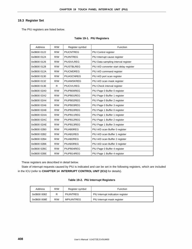
CHAPTER 19 TOUCH PANEL INTERFACE UNIT (PIU)
User’s Manual U14272EJ1V0UM00408
19.3 Register Set
The PIU registers are listed below.
Table 19-1. PIU Registers
Address R/W Register symbol Function
0x0B00 0122 R/W PIUCNTREG PIU Control register
0x0B00 0124 R/W PIUINTREG PIU Interrupt cause register
0x0B00 0126 R/W PIUSIVLREG PIU Data sampling interval register
0x0B00 0128 R/W PIUSTBLREG PIU A/D converter start delay register
0x0B00 012A R/W PIUCMDREG PIU A/D command register
0x0B00 0130 R/W PIUASCNREG PIU A/D port scan register
0x0B00 0132 R/W PIUAMSKREG PIU A/D scan mask register
0x0B00 013E R PIUCIVLREG PIU Check interval register
0x0B00 02A0 R/W PIUPB00REG PIU Page 0 Buffer 0 register
0x0B00 02A2 R/W PIUPB01REG PIU Page 0 Buffer 1 register
0x0B00 02A4 R/W PIUPB02REG PIU Page 0 Buffer 2 register
0x0B00 02A6 R/W PIUPB03REG PIU Page 0 Buffer 3 register
0x0B00 02A8 R/W PIUPB10REG PIU Page 1 Buffer 0 register
0x0B00 02AA R/W PIUPB11REG PIU Page 1 Buffer 1 register
0x0B00 02AC R/W PIUPB12REG PIU Page 1 Buffer 2 register
0x0B00 02AE R/W PIUPB13REG PIU Page 1 Buffer 3 register
0x0B00 02B0 R/W PIUAB0REG PIU A/D scan Buffer 0 register
0x0B00 02B2 R/W PIUAB1REG PIU A/D scan Buffer 1 register
0x0B00 02B4 R/W PIUAB2REG PIU A/D scan Buffer 2 register
0x0B00 02B6 R/W PIUAB3REG PIU A/D scan Buffer 3 register
0x0B00 02BC R/W PIUPB04REG PIU Page 0 Buffer 4 register
0x0B00 02BE R/W PIUPB14REG PIU Page 1 Buffer 4 register
These registers are described in detail below.
State of interrupt requests caused by PIU is indicated and can be set in the following registers, which are included
in the ICU (refer to CHAPTER 14 INTERRUPT CONTROL UNIT (ICU) for details).
Table 19-2. PIU Interrupt Registers
Address R/W Register symbol Function
0x0B00 0082 R PIUINTREG PIU interrupt indication register
0x0B00 008E R/W MPIUINTREG PIU interrupt mask register
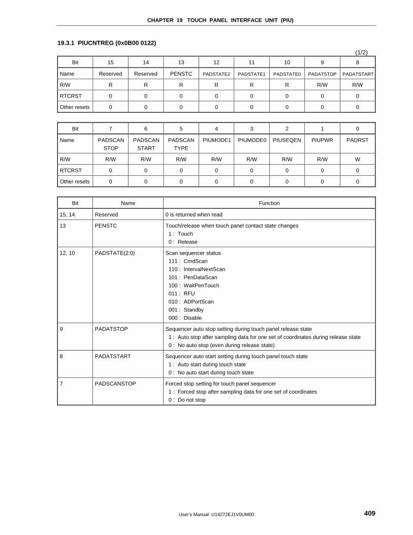
CHAPTER 19 TOUCH PANEL INTERFACE UNIT (PIU)
User’s Manual U14272EJ1V0UM00 409
19.3.1 PIUCNTREG (0x0B00 0122)
(1/2)
Bit 15 14 13 12 11 10 9 8
Name Reserved Reserved PENSTC PADSTATE2 PADSTATE1 PADSTATE0 PADATSTOP PADATSTART
R/W R R R R R R R/W R/W
RTCRST 0 0 0 0 0 0 0 0
Other resets 0 0 0 0 0 0 0 0
Bit 7 6 5 4 3 2 1 0
Name PADSCAN
STOP
PADSCAN
START
PADSCAN
TYPE
PIUMODE1 PIUMODE0 PIUSEQEN PIUPWR PADRST
R/W R/W R/W R/W R/W R/W R/W R/W W
RTCRST 0 0 0 0 0 0 0 0
Other resets 0 0 0 0 0 0 0 0
Bit Name Function
15, 14 Reserved 0 is returned when read
13 PENSTC Touch/release when touch panel contact state changes
1 : Touch
0 : Release
12, 10 PADSTATE(2:0) Scan sequencer status
111 : CmdScan
110 : IntervalNextScan
101 : PenDataScan
100 : WaitPenTouch
011 : RFU
010 : ADPortScan
001 : Standby
000 : Disable
9 PADATSTOP Sequencer auto stop setting during touch panel release state
1 : Auto stop after sampling data for one set of coordinates during release state
0 : No auto stop (even during release state)
8 PADATSTART Sequencer auto start setting during touch panel touch state
1 : Auto start during touch state
0 : No auto start during touch state
7 PADSCANSTOP Forced stop setting for touch panel sequencer
1 : Forced stop after sampling data for one set of coordinates
0 : Do not stop
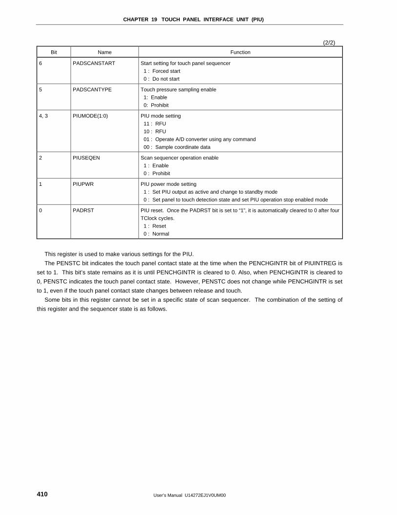
CHAPTER 19 TOUCH PANEL INTERFACE UNIT (PIU)
User’s Manual U14272EJ1V0UM00410
(2/2)
Bit Name Function
6 PADSCANSTART Start setting for touch panel sequencer
1 : Forced start
0 : Do not start
5 PADSCANTYPE Touch pressure sampling enable
1: Enable
0: Prohibit
4, 3 PIUMODE(1:0) PIU mode setting
11 : RFU
10 : RFU
01 : Operate A/D converter using any command
00 : Sample coordinate data
2 PIUSEQEN Scan sequencer operation enable
1 : Enable
0 : Prohibit
1 PIUPWR PIU power mode setting
1 : Set PIU output as active and change to standby mode
0 : Set panel to touch detection state and set PIU operation stop enabled mode
0 PADRST PIU reset. Once the PADRST bit is set to “1”, it is automatically cleared to 0 after four
TClock cycles.
1 : Reset
0 : Normal
This register is used to make various settings for the PIU.
The PENSTC bit indicates the touch panel contact state at the time when the PENCHGINTR bit of PIUINTREG is
set to 1. This bit’s state remains as it is until PENCHGINTR is cleared to 0. Also, when PENCHGINTR is cleared to
0, PENSTC indicates the touch panel contact state. However, PENSTC does not change while PENCHGINTR is set
to 1, even if the touch panel contact state changes between release and touch.
Some bits in this register cannot be set in a specific state of scan sequencer. The combination of the setting of
this register and the sequencer state is as follows.
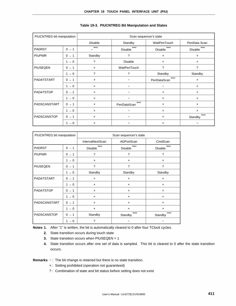
CHAPTER 19 TOUCH PANEL INTERFACE UNIT (PIU)
User’s Manual U14272EJ1V0UM00 411
Table 19-3. PIUCNTREG Bit Manipulation and States
PIUCNTREG bit manipulation Scan sequencer’s state
Disable Standby WaitPenTouch PenData Scan
PADRST 0 → 1 − Note1
Disable Note1
Disable Note1
Disable Note1
PIUPWR 0 → 1 Standby ? × ×
1 → 0 ? Disable × ×
PIUSEQEN 0 → 1 × WaitPenTouch ? ?
1 → 0 ? ? Standby Standby
PADATSTART 0 → 1 × − PenDataScan Note2
×
1 → 0 × − − ×
PADATSTOP 0 → 1 × − × ×
1 → 0 × − × ×
PADSCANSTART 0 → 1 × PenDataScan Note3
× ×
1 → 0 × − × ×
PADSCANSTOP 0 → 1 × − × Standby Note4
1 → 0 × − × −
PIUCNTREG bit manipulation Scan sequencer’s state
IntervalNextScan ADPortScan CmdScan
PADRST 0 → 1 Disable Note1
Disable Note1
Disable Note1
PIUPWR 0 → 1 ? ? ?
1 → 0 × × ×
PIUSEQEN 0 → 1 ? ? ?
1 → 0 Standby Standby Standby
PADATSTART 0 → 1 × × ×
1 → 0 × × ×
PADATSTOP 0 → 1 × × ×
1 → 0 × × ×
PADSCANSTART 0 → 1 × × ×
1 → 0 × × ×
PADSCANSTOP 0 → 1 Standby Standby Note4
Standby Note4
1 → 0 ? − −
Notes 1. After “1” is written, the bit is automatically cleared to 0 after four TClock cycles.
2. State transition occurs during touch state
3. State transition occurs when PIUSEQEN = 1
4. State transition occurs after one set of data is sampled. This bit is cleared to 0 after the state transition
occurs.
Remarks − : The bit change is retained but there is no state transition.
× : Setting prohibited (operation not guaranteed)
? : Combination of state and bit status before setting does not exist
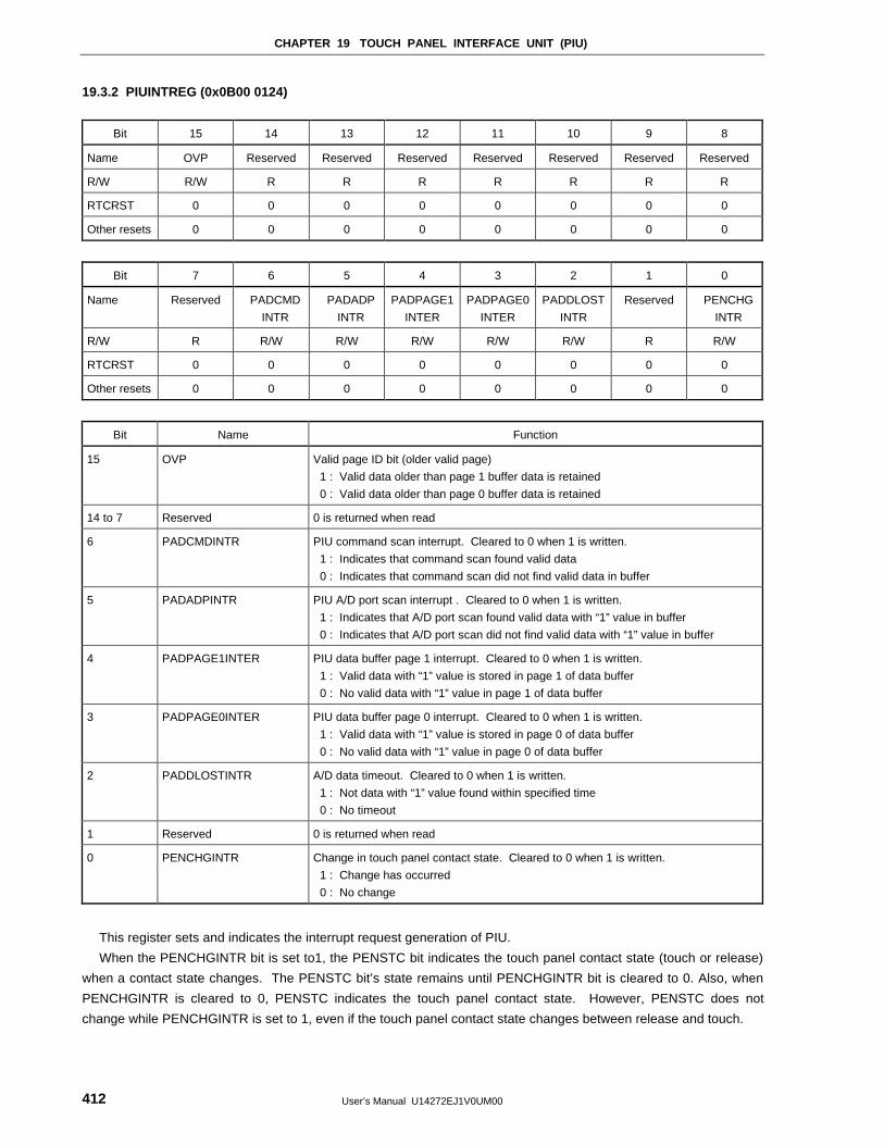
CHAPTER 19 TOUCH PANEL INTERFACE UNIT (PIU)
User’s Manual U14272EJ1V0UM00412
19.3.2 PIUINTREG (0x0B00 0124)
Bit 15 14 13 12 11 10 9 8
Name OVP Reserved Reserved Reserved Reserved Reserved Reserved Reserved
R/W R/W R R R R R R R
RTCRST 0 0 0 0 0 0 0 0
Other resets 0 0 0 0 0 0 0 0
Bit 7 6 5 4 3 2 1 0
Name Reserved PADCMD
INTR
PADADP
INTR
PADPAGE1
INTER
PADPAGE0
INTER
PADDLOST
INTR
Reserved PENCHG
INTR
R/W R R/W R/W R/W R/W R/W R R/W
RTCRST 0 0 0 0 0 0 0 0
Other resets 0 0 0 0 0 0 0 0
Bit Name Function
15 OVP Valid page ID bit (older valid page)
1 : Valid data older than page 1 buffer data is retained
0 : Valid data older than page 0 buffer data is retained
14 to 7 Reserved 0 is returned when read
6 PADCMDINTR PIU command scan interrupt. Cleared to 0 when 1 is written.
1 : Indicates that command scan found valid data
0 : Indicates that command scan did not find valid data in buffer
5 PADADPINTR PIU A/D port scan interrupt . Cleared to 0 when 1 is written.
1 : Indicates that A/D port scan found valid data with “1” value in buffer
0 : Indicates that A/D port scan did not find valid data with “1” value in buffer
4 PADPAGE1INTER PIU data buffer page 1 interrupt. Cleared to 0 when 1 is written.
1 : Valid data with “1” value is stored in page 1 of data buffer
0 : No valid data with “1” value in page 1 of data buffer
3 PADPAGE0INTER PIU data buffer page 0 interrupt. Cleared to 0 when 1 is written.
1 : Valid data with “1” value is stored in page 0 of data buffer
0 : No valid data with “1” value in page 0 of data buffer
2 PADDLOSTINTR A/D data timeout. Cleared to 0 when 1 is written.
1 : Not data with “1” value found within specified time
0 : No timeout
1 Reserved 0 is returned when read
0 PENCHGINTR Change in touch panel contact state. Cleared to 0 when 1 is written.
1 : Change has occurred
0 : No change
This register sets and indicates the interrupt request generation of PIU.
When the PENCHGINTR bit is set to1, the PENSTC bit indicates the touch panel contact state (touch or release)
when a contact state changes. The PENSTC bit’s state remains until PENCHGINTR bit is cleared to 0. Also, when
PENCHGINTR is cleared to 0, PENSTC indicates the touch panel contact state. However, PENSTC does not
change while PENCHGINTR is set to 1, even if the touch panel contact state changes between release and touch.
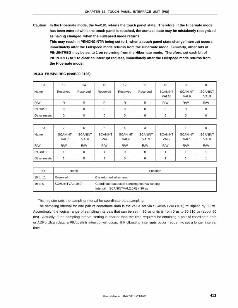
CHAPTER 19 TOUCH PANEL INTERFACE UNIT (PIU)
User’s Manual U14272EJ1V0UM00 413
Caution In the Hibernate mode, the V R4181 retains the touch panel state. Therefore, if the Hibernate mode
has been entered while the touch panel is touched, the contact state may be mistakenly recognized
as having changed, when the Fullspeed mode returns.
This may result in PENCHGINTR being set to 1, when a touch panel state change interrupt occurs
immediately after the Fullspeed mode returns from the Hibernate mode. Similarly, other bits of
PINUINTREG may be set to 1 on returning from the Hibernate mode. Therefore, set each bit of
PIUINTREG to 1 to clear an interrupt request, immediately after the Fullspeed mode returns from
the Hibernate mode.
19.3.3 PIUSIVLREG (0x0B00 0126)
Bit 15 14 13 12 11 10 9 8
Name Reserved Reserved Reserved Reserved Reserved SCANINT
VAL10
SCANINT
VAL9
SCANINT
VAL8
R/W R R R R R R/W R/W R/W
RTCRST 0 0 0 0 0 0 0 0
Other resets 0 0 0 0 0 0 0 0
Bit 7 6 5 4 3 2 1 0
Name SCANINT
VAL7
SCANINT
VAL6
SCANINT
VAL5
SCANINT
VAL4
SCANINT
VAL3
SCANINT
VAL2
SCANINT
VAL1
SCANINT
VAL0
R/W R/W R/W R/W R/W R/W R/W R/W R/W
RTCRST 1 0 1 0 0 1 1 1
Other resets 1 0 1 0 0 1 1 1
Bit Name Function
15 to 11 Reserved 0 is returned when read
10 to 0 SCANINTVAL(10:0) Coordinate data scan sampling interval setting
Interval = SCANINTVAL(10:0) x 30 µs
This register sets the sampling interval for coordinate data sampling.
The sampling interval for one pair of coordinate data is the value set via SCANINTVAL(10:0) multiplied by 30 µs.
Accordingly, the logical range of sampling intervals that can be set in 30-µs units is from 0 µs to 60,810 µs (about 60
ms). Actually, if the sampling interval setting is shorter than the time required for obtaining a pair of coordinate data
or ADPortScan data, a PIULostIntr interrupt will occur. If PIULostIntr interrupts occur frequently, set a longer interval
time.
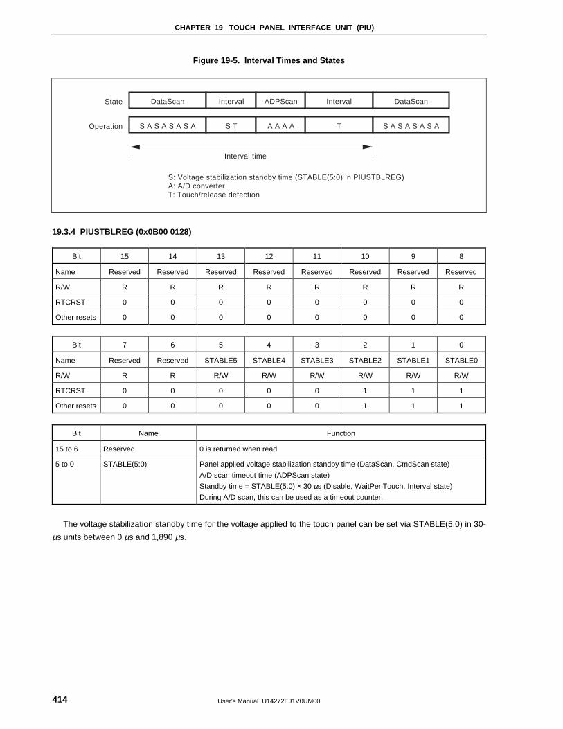
CHAPTER 19 TOUCH PANEL INTERFACE UNIT (PIU)
User’s Manual U14272EJ1V0UM00414
Figure 19-5. Interval Times and States
S: Voltage stabilization standby time (STABLE(5:0) in PIUSTBLREG)A: A/D converterT: Touch/release detection
State
Operation
DataScan Interval ADPScan Interval DataScan
S A S A S A S A
Interval time
S T A A A A T S A S A S A S A
19.3.4 PIUSTBLREG (0x0B00 0128)
Bit 15 14 13 12 11 10 9 8
Name Reserved Reserved Reserved Reserved Reserved Reserved Reserved Reserved
R/W R R R R R R R R
RTCRST 0 0 0 0 0 0 0 0
Other resets 0 0 0 0 0 0 0 0
Bit 7 6 5 4 3 2 1 0
Name Reserved Reserved STABLE5 STABLE4 STABLE3 STABLE2 STABLE1 STABLE0
R/W R R R/W R/W R/W R/W R/W R/W
RTCRST 0 0 0 0 0 1 1 1
Other resets 0 0 0 0 0 1 1 1
Bit Name Function
15 to 6 Reserved 0 is returned when read
5 to 0 STABLE(5:0) Panel applied voltage stabilization standby time (DataScan, CmdScan state)
A/D scan timeout time (ADPScan state)
Standby time = STABLE(5:0) × 30 µs (Disable, WaitPenTouch, Interval state)
During A/D scan, this can be used as a timeout counter.
The voltage stabilization standby time for the voltage applied to the touch panel can be set via STABLE(5:0) in 30-
µs units between 0 µs and 1,890 µs.
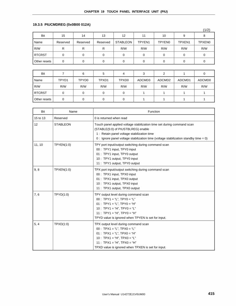
CHAPTER 19 TOUCH PANEL INTERFACE UNIT (PIU)
User’s Manual U14272EJ1V0UM00 415
19.3.5 PIUCMDREG (0x0B00 012A)
(1/2)
Bit 15 14 13 12 11 10 9 8
Name Reserved Reserved Reserved STABLEON TPYEN1 TPYEN0 TPXEN1 TPXEN0
R/W R R R R/W R/W R/W R/W R/W
RTCRST 0 0 0 0 0 0 0 0
Other resets 0 0 0 0 0 0 0 0
Bit 7 6 5 4 3 2 1 0
Name TPYD1 TPYD0 TPXD1 TPXD0 ADCMD3 ADCMD2 ADCMD1 ADCMD0
R/W R/W R/W R/W R/W R/W R/W R/W R/W
RTCRST 0 0 0 0 1 1 1 1
Other resets 0 0 0 0 1 1 1 1
Bit Name Function
15 to 13 Reserved 0 is returned when read
12 STABLEON Touch panel applied voltage stabilization time set during command scan
(STABLE(5:0) of PIUSTBLREG) enable
1 : Retain panel voltage stabilization time
0 : Ignore panel voltage stabilization time (voltage stabilization standby time = 0)
11, 10 TPYEN(1:0) TPY port input/output switching during command scan
00 : TPY1 input, TPY0 input
01 : TPY1 input, TPY0 output
10 : TPY1 output, TPY0 input
11 : TPY1 output, TPY0 output
9, 8 TPXEN(1:0) TPX port input/output switching during command scan
00 : TPX1 input, TPX0 input
01 : TPX1 input, TPX0 output
10 : TPX1 output, TPX0 input
11 : TPX1 output, TPX0 output
7, 6 TPYD(1:0) TPY output level during command scan
00 : TPY1 = “L”, TPY0 = “L”
01 : TPY1 = “L”, TPY0 = “H”
10 : TPY1 = “H”, TPY0 = “L”
11 : TPY1 = “H”, TPY0 = “H”
TPYD value is ignored when TPYEN is set for input.
5, 4 TPXD(1:0) TPX output level during command scan
00 : TPX1 = “L”, TPX0 = “L”
01 : TPX1 = “L”, TPX0 = “H”
10 : TPX1 = “H”, TPX0 = “L”
11 : TPX1 = “H”, TPX0 = “H”
TPXD value is ignored when TPXEN is set for input.
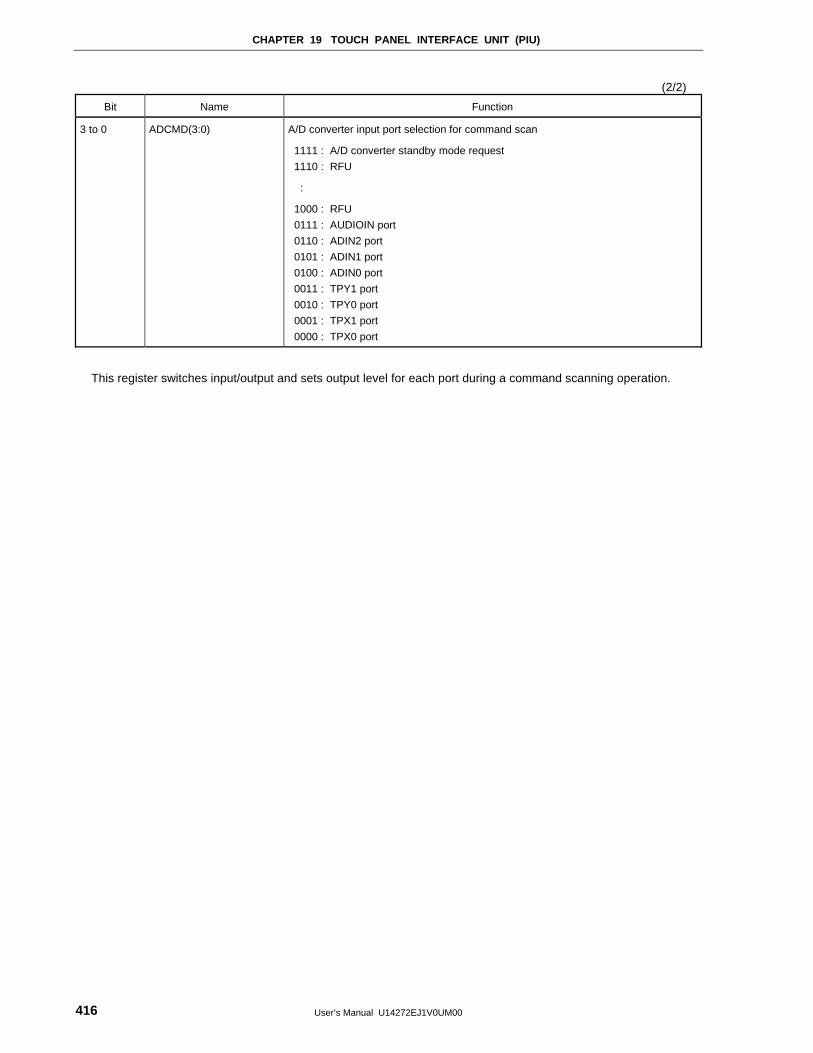
CHAPTER 19 TOUCH PANEL INTERFACE UNIT (PIU)
User’s Manual U14272EJ1V0UM00416
(2/2)
Bit Name Function
3 to 0 ADCMD(3:0) A/D converter input port selection for command scan
1111 : A/D converter standby mode request
1110 : RFU
:
1000 : RFU
0111 : AUDIOIN port
0110 : ADIN2 port
0101 : ADIN1 port
0100 : ADIN0 port
0011 : TPY1 port
0010 : TPY0 port
0001 : TPX1 port
0000 : TPX0 port
This register switches input/output and sets output level for each port during a command scanning operation.
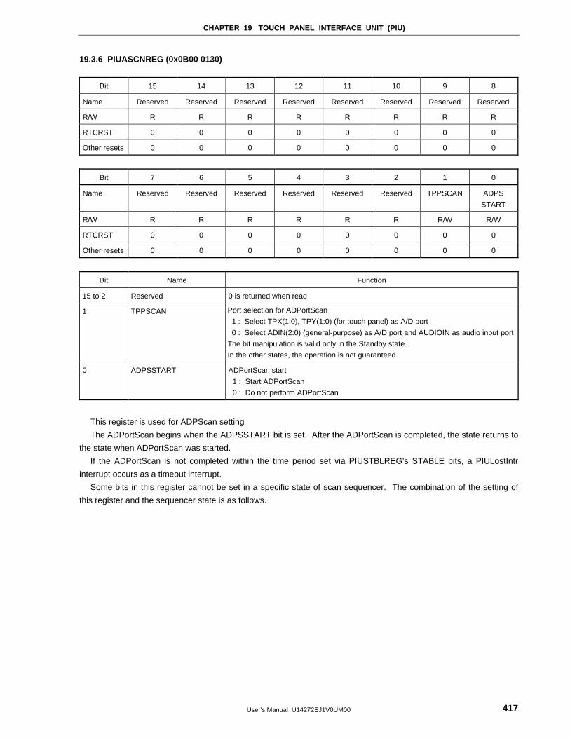
CHAPTER 19 TOUCH PANEL INTERFACE UNIT (PIU)
User’s Manual U14272EJ1V0UM00 417
19.3.6 PIUASCNREG (0x0B00 0130)
Bit 15 14 13 12 11 10 9 8
Name Reserved Reserved Reserved Reserved Reserved Reserved Reserved Reserved
R/W R R R R R R R R
RTCRST 0 0 0 0 0 0 0 0
Other resets 0 0 0 0 0 0 0 0
Bit 7 6 5 4 3 2 1 0
Name Reserved Reserved Reserved Reserved Reserved Reserved TPPSCAN ADPS
START
R/W R R R R R R R/W R/W
RTCRST 0 0 0 0 0 0 0 0
Other resets 0 0 0 0 0 0 0 0
Bit Name Function
15 to 2 Reserved 0 is returned when read
1 TPPSCAN Port selection for ADPortScan
1 : Select TPX(1:0), TPY(1:0) (for touch panel) as A/D port
0 : Select ADIN(2:0) (general-purpose) as A/D port and AUDIOIN as audio input port
The bit manipulation is valid only in the Standby state.
In the other states, the operation is not guaranteed.
0 ADPSSTART ADPortScan start
1 : Start ADPortScan
0 : Do not perform ADPortScan
This register is used for ADPScan setting
The ADPortScan begins when the ADPSSTART bit is set. After the ADPortScan is completed, the state returns to
the state when ADPortScan was started.
If the ADPortScan is not completed within the time period set via PIUSTBLREG’s STABLE bits, a PIULostIntr
interrupt occurs as a timeout interrupt.
Some bits in this register cannot be set in a specific state of scan sequencer. The combination of the setting of
this register and the sequencer state is as follows.
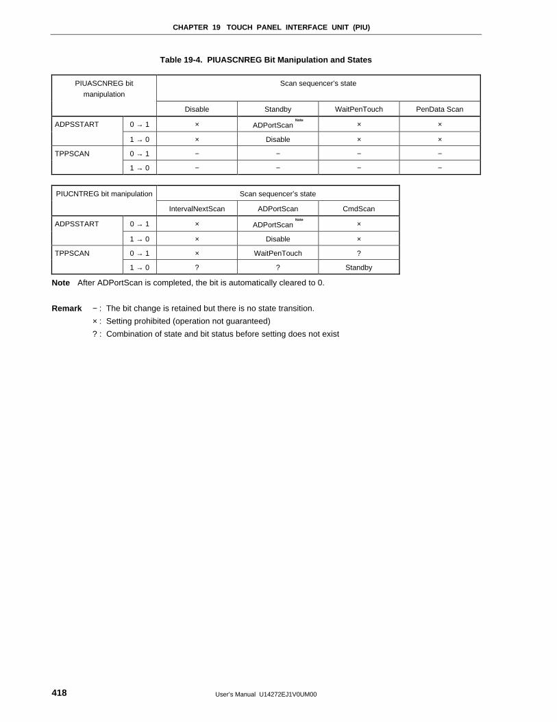
CHAPTER 19 TOUCH PANEL INTERFACE UNIT (PIU)
User’s Manual U14272EJ1V0UM00418
Table 19-4. PIUASCNREG Bit Manipulation and States
PIUASCNREG bit
manipulation
Scan sequencer’s state
Disable Standby WaitPenTouch PenData Scan
ADPSSTART 0 → 1 × ADPortScan Note
× ×
1 → 0 × Disable × ×
TPPSCAN 0 → 1 − − − −
1 → 0 − − − −
PIUCNTREG bit manipulation Scan sequencer’s state
IntervalNextScan ADPortScan CmdScan
ADPSSTART 0 → 1 × ADPortScan Note
×
1 → 0 × Disable ×
TPPSCAN 0 → 1 × WaitPenTouch ?
1 → 0 ? ? Standby
Note After ADPortScan is completed, the bit is automatically cleared to 0.
Remark − : The bit change is retained but there is no state transition.
× : Setting prohibited (operation not guaranteed)
? : Combination of state and bit status before setting does not exist
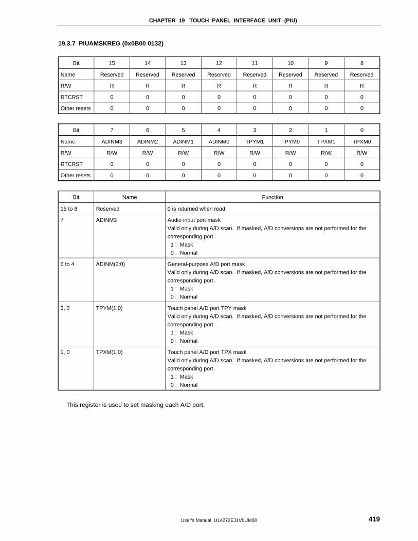
CHAPTER 19 TOUCH PANEL INTERFACE UNIT (PIU)
User’s Manual U14272EJ1V0UM00 419
19.3.7 PIUAMSKREG (0x0B00 0132)
Bit 15 14 13 12 11 10 9 8
Name Reserved Reserved Reserved Reserved Reserved Reserved Reserved Reserved
R/W R R R R R R R R
RTCRST 0 0 0 0 0 0 0 0
Other resets 0 0 0 0 0 0 0 0
Bit 7 6 5 4 3 2 1 0
Name ADINM3 ADINM2 ADINM1 ADINM0 TPYM1 TPYM0 TPXM1 TPXM0
R/W R/W R/W R/W R/W R/W R/W R/W R/W
RTCRST 0 0 0 0 0 0 0 0
Other resets 0 0 0 0 0 0 0 0
Bit Name Function
15 to 8 Reserved 0 is returned when read
7 ADINM3 Audio input port mask
Valid only during A/D scan. If masked, A/D conversions are not performed for the
corresponding port.
1 : Mask
0 : Normal
6 to 4 ADINM(2:0) General-purpose A/D port mask
Valid only during A/D scan. If masked, A/D conversions are not performed for the
corresponding port.
1 : Mask
0 : Normal
3, 2 TPYM(1:0) Touch panel A/D port TPY mask
Valid only during A/D scan. If masked, A/D conversions are not performed for the
corresponding port.
1 : Mask
0 : Normal
1, 0 TPXM(1:0) Touch panel A/D port TPX mask
Valid only during A/D scan. If masked, A/D conversions are not performed for the
corresponding port.
1 : Mask
0 : Normal
This register is used to set masking each A/D port.
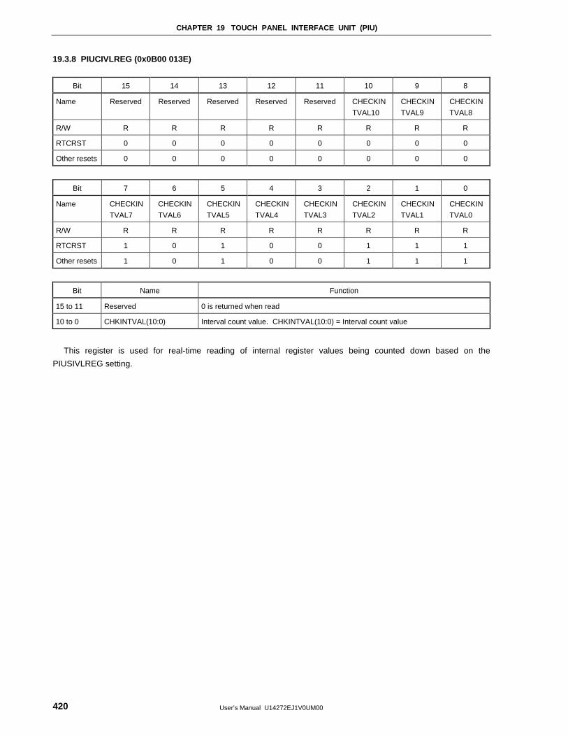
CHAPTER 19 TOUCH PANEL INTERFACE UNIT (PIU)
User’s Manual U14272EJ1V0UM00420
19.3.8 PIUCIVLREG (0x0B00 013E)
Bit 15 14 13 12 11 10 9 8
Name Reserved Reserved Reserved Reserved Reserved CHECKIN
TVAL10
CHECKIN
TVAL9
CHECKIN
TVAL8
R/W R R R R R R R R
RTCRST 0 0 0 0 0 0 0 0
Other resets 0 0 0 0 0 0 0 0
Bit 7 6 5 4 3 2 1 0
Name CHECKIN
TVAL7
CHECKIN
TVAL6
CHECKIN
TVAL5
CHECKIN
TVAL4
CHECKIN
TVAL3
CHECKIN
TVAL2
CHECKIN
TVAL1
CHECKIN
TVAL0
R/W R R R R R R R R
RTCRST 1 0 1 0 0 1 1 1
Other resets 1 0 1 0 0 1 1 1
Bit Name Function
15 to 11 Reserved 0 is returned when read
10 to 0 CHKINTVAL(10:0) Interval count value. CHKINTVAL(10:0) = Interval count value
This register is used for real-time reading of internal register values being counted down based on the
PIUSIVLREG setting.
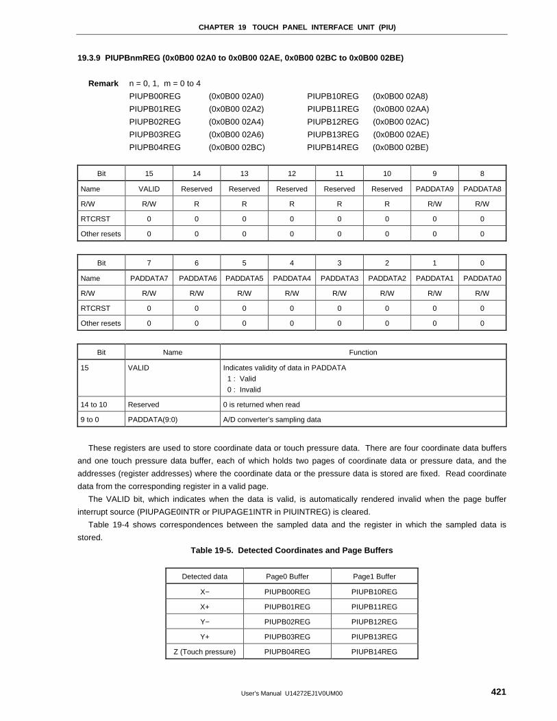
CHAPTER 19 TOUCH PANEL INTERFACE UNIT (PIU)
User’s Manual U14272EJ1V0UM00 421
19.3.9 PIUPBnmREG (0x0B00 02A0 to 0x0B00 02AE, 0x0B00 02BC to 0x0B00 02BE)
Remark n = 0, 1, m = 0 to 4
PIUPB00REG (0x0B00 02A0) PIUPB10REG (0x0B00 02A8)
PIUPB01REG (0x0B00 02A2) PIUPB11REG (0x0B00 02AA)
PIUPB02REG (0x0B00 02A4) PIUPB12REG (0x0B00 02AC)
PIUPB03REG (0x0B00 02A6) PIUPB13REG (0x0B00 02AE)
PIUPB04REG (0x0B00 02BC) PIUPB14REG (0x0B00 02BE)
Bit 15 14 13 12 11 10 9 8
Name VALID Reserved Reserved Reserved Reserved Reserved PADDATA9 PADDATA8
R/W R/W R R R R R R/W R/W
RTCRST 0 0 0 0 0 0 0 0
Other resets 0 0 0 0 0 0 0 0
Bit 7 6 5 4 3 2 1 0
Name PADDATA7 PADDATA6 PADDATA5 PADDATA4 PADDATA3 PADDATA2 PADDATA1 PADDATA0
R/W R/W R/W R/W R/W R/W R/W R/W R/W
RTCRST 0 0 0 0 0 0 0 0
Other resets 0 0 0 0 0 0 0 0
Bit Name Function
15 VALID Indicates validity of data in PADDATA
1 : Valid
0 : Invalid
14 to 10 Reserved 0 is returned when read
9 to 0 PADDATA(9:0) A/D converter’s sampling data
These registers are used to store coordinate data or touch pressure data. There are four coordinate data buffers
and one touch pressure data buffer, each of which holds two pages of coordinate data or pressure data, and the
addresses (register addresses) where the coordinate data or the pressure data is stored are fixed. Read coordinate
data from the corresponding register in a valid page.
The VALID bit, which indicates when the data is valid, is automatically rendered invalid when the page buffer
interrupt source (PIUPAGE0INTR or PIUPAGE1INTR in PIUINTREG) is cleared.
Table 19-4 shows correspondences between the sampled data and the register in which the sampled data is
stored.
Table 19-5. Detected Coordinates and Page Buffers
Detected data Page0 Buffer Page1 Buffer
X− PIUPB00REG PIUPB10REG
X+ PIUPB01REG PIUPB11REG
Y− PIUPB02REG PIUPB12REG
Y+ PIUPB03REG PIUPB13REG
Z (Touch pressure) PIUPB04REG PIUPB14REG
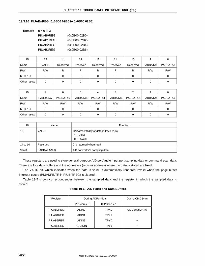
CHAPTER 19 TOUCH PANEL INTERFACE UNIT (PIU)
User’s Manual U14272EJ1V0UM00422
19.3.10 PIUABnREG (0x0B00 02B0 to 0x0B00 02B6)
Remark n = 0 to 3
PIUAB0REG (0x0B00 02B0)
PIUAB1REG (0x0B00 02B2)
PIUAB2REG (0x0B00 02B4)
PIUAB3REG (0x0B00 02B6)
Bit 15 14 13 12 11 10 9 8
Name VALID Reserved Reserved Reserved Reserved Reserved PADDATA9 PADDATA8
R/W R/W R R R R R R/W R/W
RTCRST 0 0 0 0 0 0 0 0
Other resets 0 0 0 0 0 0 0 0
Bit 7 6 5 4 3 2 1 0
Name PADDATA7 PADDATA6 PADDATA5 PADDATA4 PADDATA3 PADDATA2 PADDATA1 PADDATA0
R/W R/W R/W R/W R/W R/W R/W R/W R/W
RTCRST 0 0 0 0 0 0 0 0
Other resets 0 0 0 0 0 0 0 0
Bit Name Function
15 VALID Indicates validity of data in PADDATA
1 : Valid
0 : Invalid
14 to 10 Reserved 0 is returned when read
9 to 0 PADDATA(9:0) A/D converter’s sampling data
These registers are used to store general-purpose A/D port/audio input port sampling data or command scan data.
There are four data buffers and the addresses (register address) where the data is stored are fixed.
The VALID bit, which indicates when the data is valid, is automatically rendered invalid when the page buffer
interrupt cause (PIUADPINTR in PIUINTREG) is cleared.
Table 19-5 shows correspondences between the sampled data and the register in which the sampled data is
stored.
Table 19-6. A/D Ports and Data Buffers
Register During ADPortScan During CMDScan
TPPScan = 0 TPPScan = 1
PIUAB0REG
PIUAB1REG
PIUAB2REG
PIUAB3REG
ADIN0
ADIN1
ADIN2
AUDIOIN
TPX0
TPX1
TPY0
TPY1
CMDScanDATA
−
−
−
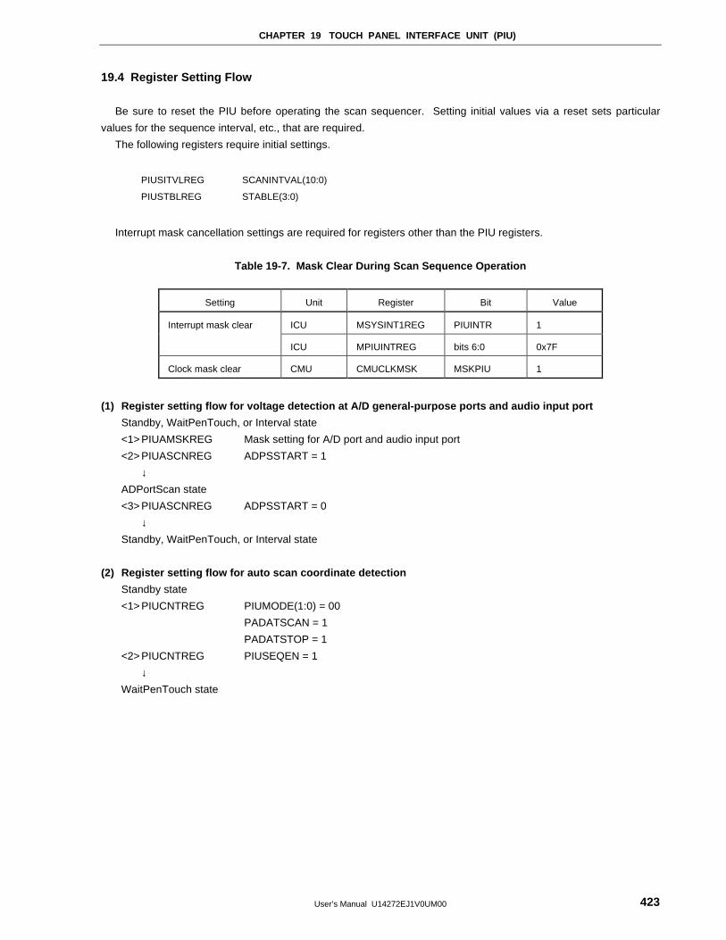
CHAPTER 19 TOUCH PANEL INTERFACE UNIT (PIU)
User’s Manual U14272EJ1V0UM00 423
19.4 Register Setting Flow
Be sure to reset the PIU before operating the scan sequencer. Setting initial values via a reset sets particular
values for the sequence interval, etc., that are required.
The following registers require initial settings.
PIUSITVLREG SCANINTVAL(10:0)
PIUSTBLREG STABLE(3:0)
Interrupt mask cancellation settings are required for registers other than the PIU registers.
Table 19-7. Mask Clear During Scan Sequence Operation
Setting Unit Register Bit Value
Interrupt mask clear ICU MSYSINT1REG PIUINTR 1
ICU MPIUINTREG bits 6:0 0x7F
Clock mask clear CMU CMUCLKMSK MSKPIU 1
(1) Register setting flow for voltage detection at A/D general-purpose ports and audio input port
Standby, WaitPenTouch, or Interval state
<1> PIUAMSKREG Mask setting for A/D port and audio input port
<2> PIUASCNREG ADPSSTART = 1
↓ADPortScan state
<3> PIUASCNREG ADPSSTART = 0
↓Standby, WaitPenTouch, or Interval state
(2) Register setting flow for auto scan coordinate detection
Standby state
<1> PIUCNTREG PIUMODE(1:0) = 00
PADATSCAN = 1
PADATSTOP = 1
<2> PIUCNTREG PIUSEQEN = 1
↓WaitPenTouch state
CHAPTER 19 TOUCH PANEL INTERFACE UNIT (PIU)
User’s Manual U14272EJ1V0UM00424
(3) Register setting flow for manual scan coordinate detection
Disable state
<1> PIUCNTREG PIUPWR = 1
↓Standby state
<2> PIUCNTREG PIUMODE(1:0) = 00
PADSCANSTART = 1
<3> PIUCNTREG PIUSEQEN = 1
↓PenDataScan state
(4) Register setting flow during Suspend mode transition
Standby, WaitPenTouch, or Interval state
<1> PIUCNTREG PIUSEQEN = 0
↓Standby state
<2> PIUCNTREG PIUPWR = 1
↓Disable state
(5) Register setting flow when returning from Suspend mode transition
Disable state
<1> PIUCNTREG PIUPWR = 1
↓Standby state
<2> PIUCNTREG PIUMODE(1:0) = 00
PADATSCAN = 1
PADATSTOP = 1
<3> PIUCNTREG PIUSEQEN = 1
↓WaitPenTouch state
Touch detected
↓PenDataScan state
(6) Register setting flow for command scan
Disable state
<1> PIUCNTREG PIUPWR = 1
↓Standby state
<2> PIUCNTREG PIUMODE(1:0) = 01
<3> PIUCNTREG Set touch panel pins, select input port
<4> PIUCNTREG PIUSEQEN = 1
↓CMDScan state
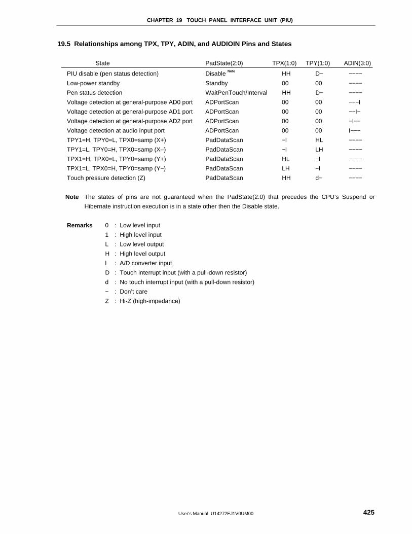
CHAPTER 19 TOUCH PANEL INTERFACE UNIT (PIU)
User’s Manual U14272EJ1V0UM00 425
19.5 Relationships among TPX, TPY, ADIN, and AUDIOIN Pins and States
State PadState(2:0) TPX(1:0) TPY(1:0) ADIN(3:0)
PIU disable (pen status detection) Disable Note HH D− −−−−Low-power standby Standby 00 00 −−−−Pen status detection WaitPenTouch/Interval HH D− −−−−Voltage detection at general-purpose AD0 port ADPortScan 00 00 −−−I
Voltage detection at general-purpose AD1 port ADPortScan 00 00 −−I−Voltage detection at general-purpose AD2 port ADPortScan 00 00 −I−−Voltage detection at audio input port ADPortScan 00 00 I−−−TPY1=H, TPY0=L, TPX0=samp (X+) PadDataScan −I HL −−−−TPY1=L, TPY0=H, TPX0=samp (X–) PadDataScan −I LH −−−−TPX1=H, TPX0=L, TPY0=samp (Y+) PadDataScan HL −I −−−−TPX1=L, TPX0=H, TPY0=samp (Y−) PadDataScan LH −I −−−−Touch pressure detection (Z) PadDataScan HH d− −−−−
Note The states of pins are not guaranteed when the PadState(2:0) that precedes the CPU’s Suspend or
Hibernate instruction execution is in a state other then the Disable state.
Remarks 0 : Low level input
1 : High level input
L : Low level output
H : High level output
l : A/D converter input
D : Touch interrupt input (with a pull-down resistor)
d : No touch interrupt input (with a pull-down resistor)
− : Don’t care
Z : Hi-Z (high-impedance)
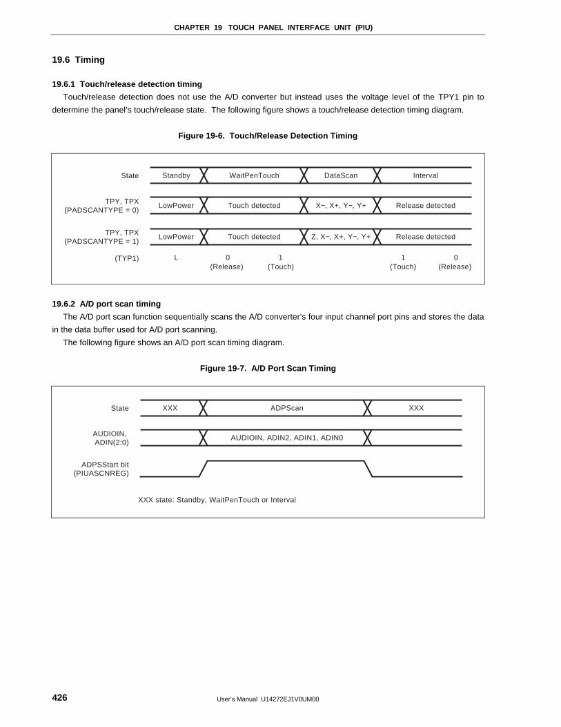
CHAPTER 19 TOUCH PANEL INTERFACE UNIT (PIU)
User’s Manual U14272EJ1V0UM00426
19.6 Timing
19.6.1 Touch/release detection timing
Touch/release detection does not use the A/D converter but instead uses the voltage level of the TPY1 pin to
determine the panel’s touch/release state. The following figure shows a touch/release detection timing diagram.
Figure 19-6. Touch/Release Detection Timing
State Standby WaitPenTouch DataScan Interval
TPY, TPX(PADSCANTYPE = 0)
LowPower Touch detected X−, X+, Y−, Y+ Release detected
TPY, TPX(PADSCANTYPE = 1)
LowPower Touch detected Z, X−, X+, Y−, Y+ Release detected
(TYP1) L 0 1(Release) (Touch)
1 0 (Touch) (Release)
19.6.2 A/D port scan timing
The A/D port scan function sequentially scans the A/D converter’s four input channel port pins and stores the data
in the data buffer used for A/D port scanning.
The following figure shows an A/D port scan timing diagram.
Figure 19-7. A/D Port Scan Timing
State XXX ADPScan XXX
AUDIOIN, ADIN(2:0)
AUDIOIN, ADIN2, ADIN1, ADIN0
ADPSStart bit(PIUASCNREG)
XXX state: Standby, WaitPenTouch or Interval
CHAPTER 19 TOUCH PANEL INTERFACE UNIT (PIU)
User’s Manual U14272EJ1V0UM00 427
19.7 Data Loss Interrupt Conditions
The PIU issues a PIUDataLostIntr interrupt when any of the following four conditions exist.
Once a PIUDataLostIntr interrupt occurs, the sequencer is forcibly changed to the Standby state.
1. Data for one coordinate has not been obtained within the interval period
2. The A/D port scan has not been completed within the time set via PIUSTBLREG
3. Transfer of the next coordinate data has begun while valid data for both pages remains in the buffer
4. The next data transfer starts while there is valid data in the ADPortScan buffer
(1) When data for one coordinate has not been obtained within the interval period
Cause
This condition occurs when the AIU has exclusive use of the A/D converter and the PIU is therefore unable to
use the A/D converter.
If this data loss condition occurs frequently, implement a countermeasure that temporarily prohibits the AIU’s
use of the A/D converter.
Response
After clearing the cause of the PIUDataLostIntr interrupt, set PIUCIUCNTREG’s PADATSTART bit or
PADSCANSTART bit to restart the coordinate detection operation. Once the PIUDataLostIntr interrupt is
cleared, the page in which the loss occurred becomes invalid. If the valid data prior to the data loss is
needed, be sure to save the data that is being stored in the page buffer before clearing the PIUDataLostIntr
interrupt.
(2) When the A/D port scan has not been completed within the time set via PIUSTBLREG
Cause
Same as cause of condition 1
Response
After clearing the cause of the PIUDataLostIntr interrupt, set PIUASCNREG’s ADPSSTART bit to restart the
A/D port scan operation. Once the PIUDataLostIntr interrupt is cleared, the page in which the loss occurred
becomes invalid. If the valid data prior to the data loss is needed, be sure to save the data that is being
stored in the page buffer before clearing the PIUDataLostIntr interrupt.
(3) When transfer of the next coordinate data has begun while valid data for both pages remains in the buffer
Cause
This condition is caused when the data buffer contains two pages of valid data (both the PIUPAGE1INTR and
PIUPAGE0INTR interrupts have occurred) but the valid data has not been processed. If the A/D converter is
used frequently, this may shorten the time that would normally be required from when both pages become full
until when the data loss occurs.
Response
In condition 3, valid data contained in the pages when the PIUDataLostIntr interrupt occurs is never
overwritten.
After two pages of valid data are processed, clear the causes of the three interrupts (PIUDataLostIntr,
PIUPAGE1INTR, and PIUPAGE0INTR).
After clearing these interrupt causes, set the PADATSTART bit or PADSCANSTART bit of PIUCIUCNTREG
to restart the coordinate detection operation.
CHAPTER 19 TOUCH PANEL INTERFACE UNIT (PIU)
User’s Manual U14272EJ1V0UM00428
(4) When the next data transfer starts while there is valid data in the ADPortScan buffer
Cause
This condition is caused when valid data is not processed even while the ADPortScan buffer holds valid data
(PADADPINTR interrupt occurrence).
Response
In condition 4, valid data contained in the buffer when the PIUDataLostIntr interrupt occurs is never
overwritten.
After valid data in the buffer is processed, clear the causes of the two interrupts (PIUDataLostIntr,
PADADPINTR).
After clearing these interrupt causes, set the ADPSSTART bit of PIUASCNREG to restart the general-
purpose A/D port scan.
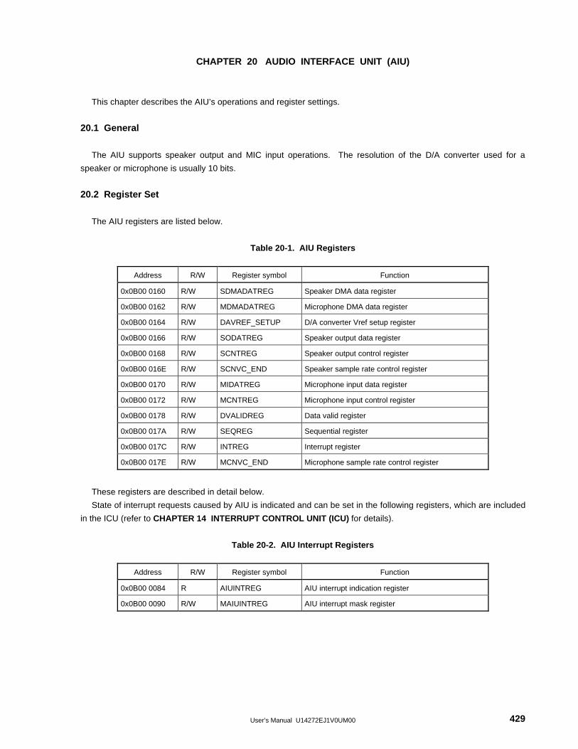
User’s Manual U14272EJ1V0UM00 429
CHAPTER 20 AUDIO INTERFACE UNIT (AIU)
This chapter describes the AIU’s operations and register settings.
20.1 General
The AIU supports speaker output and MIC input operations. The resolution of the D/A converter used for a
speaker or microphone is usually 10 bits.
20.2 Register Set
The AIU registers are listed below.
Table 20-1. AIU Registers
Address R/W Register symbol Function
0x0B00 0160 R/W SDMADATREG Speaker DMA data register
0x0B00 0162 R/W MDMADATREG Microphone DMA data register
0x0B00 0164 R/W DAVREF_SETUP D/A converter Vref setup register
0x0B00 0166 R/W SODATREG Speaker output data register
0x0B00 0168 R/W SCNTREG Speaker output control register
0x0B00 016E R/W SCNVC_END Speaker sample rate control register
0x0B00 0170 R/W MIDATREG Microphone input data register
0x0B00 0172 R/W MCNTREG Microphone input control register
0x0B00 0178 R/W DVALIDREG Data valid register
0x0B00 017A R/W SEQREG Sequential register
0x0B00 017C R/W INTREG Interrupt register
0x0B00 017E R/W MCNVC_END Microphone sample rate control register
These registers are described in detail below.
State of interrupt requests caused by AIU is indicated and can be set in the following registers, which are included
in the ICU (refer to CHAPTER 14 INTERRUPT CONTROL UNIT (ICU) for details).
Table 20-2. AIU Interrupt Registers
Address R/W Register symbol Function
0x0B00 0084 R AIUINTREG AIU interrupt indication register
0x0B00 0090 R/W MAIUINTREG AIU interrupt mask register
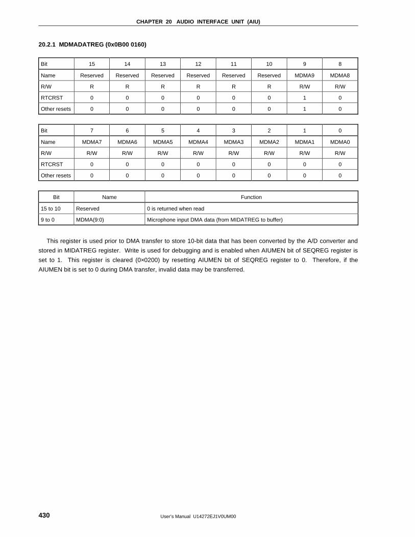
CHAPTER 20 AUDIO INTERFACE UNIT (AIU)
User’s Manual U14272EJ1V0UM00430
20.2.1 MDMADATREG (0x0B00 0160)
Bit 15 14 13 12 11 10 9 8
Name Reserved Reserved Reserved Reserved Reserved Reserved MDMA9 MDMA8
R/W R R R R R R R/W R/W
RTCRST 0 0 0 0 0 0 1 0
Other resets 0 0 0 0 0 0 1 0
Bit 7 6 5 4 3 2 1 0
Name MDMA7 MDMA6 MDMA5 MDMA4 MDMA3 MDMA2 MDMA1 MDMA0
R/W R/W R/W R/W R/W R/W R/W R/W R/W
RTCRST 0 0 0 0 0 0 0 0
Other resets 0 0 0 0 0 0 0 0
Bit Name Function
15 to 10 Reserved 0 is returned when read
9 to 0 MDMA(9:0) Microphone input DMA data (from MIDATREG to buffer)
This register is used prior to DMA transfer to store 10-bit data that has been converted by the A/D converter and
stored in MIDATREG register. Write is used for debugging and is enabled when AIUMEN bit of SEQREG register is
set to 1. This register is cleared (0×0200) by resetting AIUMEN bit of SEQREG register to 0. Therefore, if the
AIUMEN bit is set to 0 during DMA transfer, invalid data may be transferred.
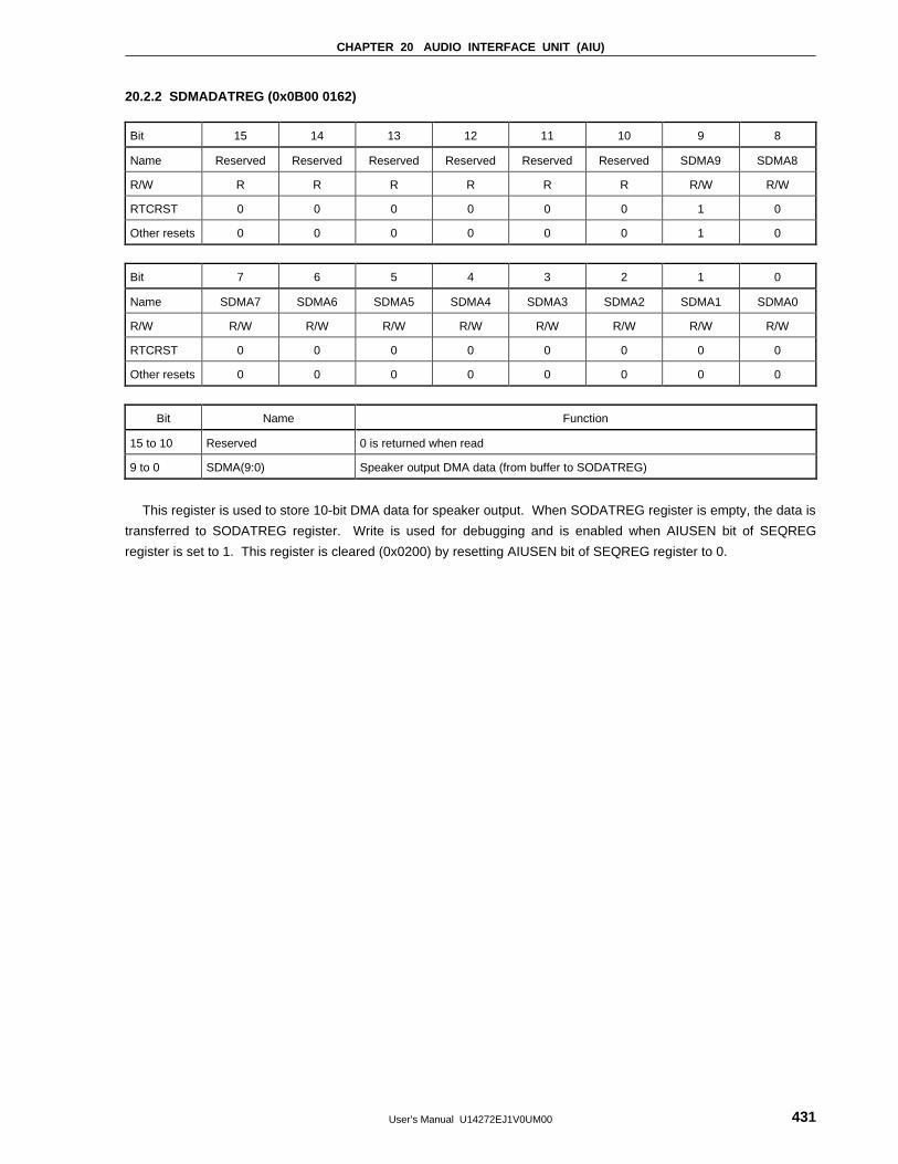
CHAPTER 20 AUDIO INTERFACE UNIT (AIU)
User’s Manual U14272EJ1V0UM00 431
20.2.2 SDMADATREG (0x0B00 0162)
Bit 15 14 13 12 11 10 9 8
Name Reserved Reserved Reserved Reserved Reserved Reserved SDMA9 SDMA8
R/W R R R R R R R/W R/W
RTCRST 0 0 0 0 0 0 1 0
Other resets 0 0 0 0 0 0 1 0
Bit 7 6 5 4 3 2 1 0
Name SDMA7 SDMA6 SDMA5 SDMA4 SDMA3 SDMA2 SDMA1 SDMA0
R/W R/W R/W R/W R/W R/W R/W R/W R/W
RTCRST 0 0 0 0 0 0 0 0
Other resets 0 0 0 0 0 0 0 0
Bit Name Function
15 to 10 Reserved 0 is returned when read
9 to 0 SDMA(9:0) Speaker output DMA data (from buffer to SODATREG)
This register is used to store 10-bit DMA data for speaker output. When SODATREG register is empty, the data is
transferred to SODATREG register. Write is used for debugging and is enabled when AIUSEN bit of SEQREG
register is set to 1. This register is cleared (0x0200) by resetting AIUSEN bit of SEQREG register to 0.
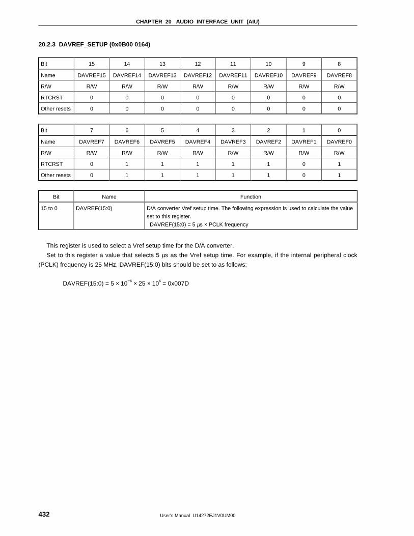
CHAPTER 20 AUDIO INTERFACE UNIT (AIU)
User’s Manual U14272EJ1V0UM00432
20.2.3 DAVREF_SETUP (0x0B00 0164)
Bit 15 14 13 12 11 10 9 8
Name DAVREF15 DAVREF14 DAVREF13 DAVREF12 DAVREF11 DAVREF10 DAVREF9 DAVREF8
R/W R/W R/W R/W R/W R/W R/W R/W R/W
RTCRST 0 0 0 0 0 0 0 0
Other resets 0 0 0 0 0 0 0 0
Bit 7 6 5 4 3 2 1 0
Name DAVREF7 DAVREF6 DAVREF5 DAVREF4 DAVREF3 DAVREF2 DAVREF1 DAVREF0
R/W R/W R/W R/W R/W R/W R/W R/W R/W
RTCRST 0 1 1 1 1 1 0 1
Other resets 0 1 1 1 1 1 0 1
Bit Name Function
15 to 0 DAVREF(15:0) D/A converter Vref setup time. The following expression is used to calculate the value
set to this register.
DAVREF(15:0) = 5 µs × PCLK frequency
This register is used to select a Vref setup time for the D/A converter.
Set to this register a value that selects 5 µs as the Vref setup time. For example, if the internal peripheral clock
(PCLK) frequency is 25 MHz, DAVREF(15:0) bits should be set to as follows;
DAVREF(15:0) = 5 × 10−6 × 25 × 106 = 0x007D
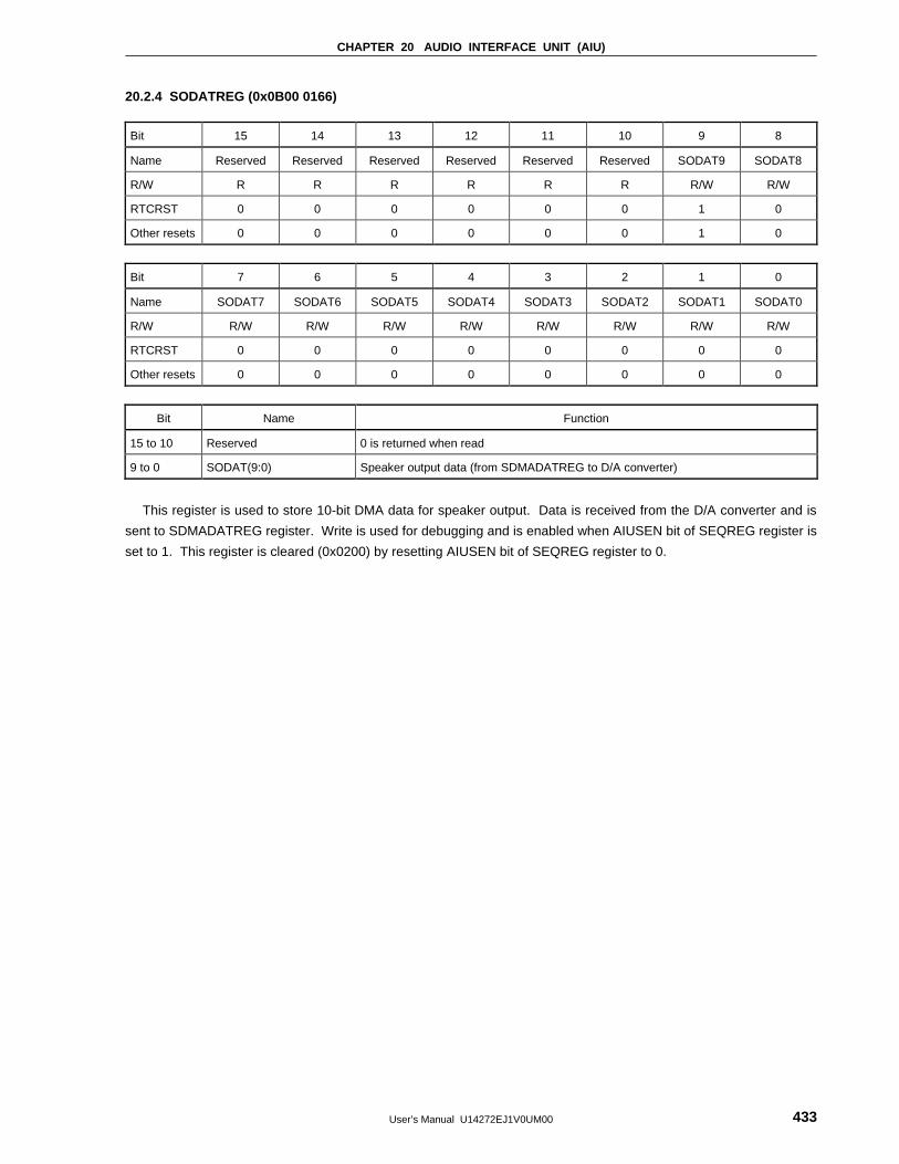
CHAPTER 20 AUDIO INTERFACE UNIT (AIU)
User’s Manual U14272EJ1V0UM00 433
20.2.4 SODATREG (0x0B00 0166)
Bit 15 14 13 12 11 10 9 8
Name Reserved Reserved Reserved Reserved Reserved Reserved SODAT9 SODAT8
R/W R R R R R R R/W R/W
RTCRST 0 0 0 0 0 0 1 0
Other resets 0 0 0 0 0 0 1 0
Bit 7 6 5 4 3 2 1 0
Name SODAT7 SODAT6 SODAT5 SODAT4 SODAT3 SODAT2 SODAT1 SODAT0
R/W R/W R/W R/W R/W R/W R/W R/W R/W
RTCRST 0 0 0 0 0 0 0 0
Other resets 0 0 0 0 0 0 0 0
Bit Name Function
15 to 10 Reserved 0 is returned when read
9 to 0 SODAT(9:0) Speaker output data (from SDMADATREG to D/A converter)
This register is used to store 10-bit DMA data for speaker output. Data is received from the D/A converter and is
sent to SDMADATREG register. Write is used for debugging and is enabled when AIUSEN bit of SEQREG register is
set to 1. This register is cleared (0x0200) by resetting AIUSEN bit of SEQREG register to 0.
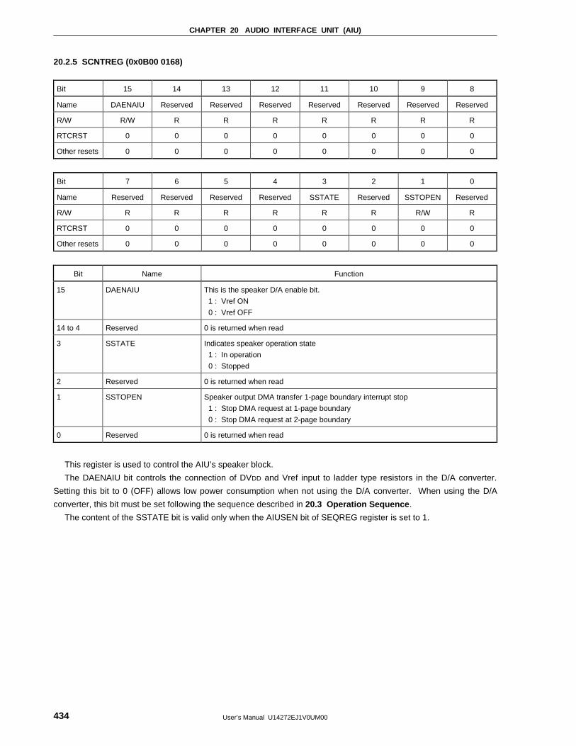
CHAPTER 20 AUDIO INTERFACE UNIT (AIU)
User’s Manual U14272EJ1V0UM00434
20.2.5 SCNTREG (0x0B00 0168)
Bit 15 14 13 12 11 10 9 8
Name DAENAIU Reserved Reserved Reserved Reserved Reserved Reserved Reserved
R/W R/W R R R R R R R
RTCRST 0 0 0 0 0 0 0 0
Other resets 0 0 0 0 0 0 0 0
Bit 7 6 5 4 3 2 1 0
Name Reserved Reserved Reserved Reserved SSTATE Reserved SSTOPEN Reserved
R/W R R R R R R R/W R
RTCRST 0 0 0 0 0 0 0 0
Other resets 0 0 0 0 0 0 0 0
Bit Name Function
15 DAENAIU This is the speaker D/A enable bit.
1 : Vref ON
0 : Vref OFF
14 to 4 Reserved 0 is returned when read
3 SSTATE Indicates speaker operation state
1 : In operation
0 : Stopped
2 Reserved 0 is returned when read
1 SSTOPEN Speaker output DMA transfer 1-page boundary interrupt stop
1 : Stop DMA request at 1-page boundary
0 : Stop DMA request at 2-page boundary
0 Reserved 0 is returned when read
This register is used to control the AIU’s speaker block.
The DAENAIU bit controls the connection of DVDD and Vref input to ladder type resistors in the D/A converter.
Setting this bit to 0 (OFF) allows low power consumption when not using the D/A converter. When using the D/A
converter, this bit must be set following the sequence described in 20.3 Operation Sequence .
The content of the SSTATE bit is valid only when the AIUSEN bit of SEQREG register is set to 1.
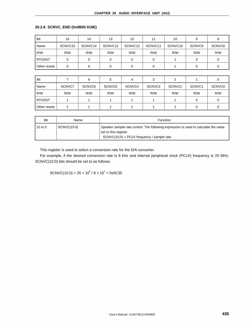
CHAPTER 20 AUDIO INTERFACE UNIT (AIU)
User’s Manual U14272EJ1V0UM00 435
20.2.6 SCNVC_END (0x0B00 016E)
Bit 15 14 13 12 11 10 9 8
Name SCNVC15 SCNVC14 SCNVC13 SCNVC12 SCNVC11 SCNVC10 SCNVC9 SCNVC8
R/W R/W R/W R/W R/W R/W R/W R/W R/W
RTCRST 0 0 0 0 0 1 0 0
Other resets 0 0 0 0 0 1 0 0
Bit 7 6 5 4 3 2 1 0
Name SCNVC7 SCNVC6 SCNVC5 SCNVC4 SCNVC3 SCNVC2 SCNVC1 SCNVC0
R/W R/W R/W R/W R/W R/W R/W R/W R/W
RTCRST 1 1 1 1 1 1 0 0
Other resets 1 1 1 1 1 1 0 0
Bit Name Function
15 to 0 SCNVC(15:0) Speaker sample rate control. The following expression is used to calculate the value
set to this register.
SCNVC(15:0) = PCLK frequency / sample rate
This register is used to select a conversion rate for the D/A converter.
For example, if the desired conversion rate is 8 kHz and internal peripheral clock (PCLK) frequency is 25 MHz,
SCNVC(15:0) bits should be set to as follows;
SCNVC(15:0) = 25 × 106 / 8 × 103 = 0x0C35
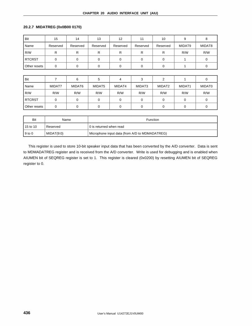
CHAPTER 20 AUDIO INTERFACE UNIT (AIU)
User’s Manual U14272EJ1V0UM00436
20.2.7 MIDATREG (0x0B00 0170)
Bit 15 14 13 12 11 10 9 8
Name Reserved Reserved Reserved Reserved Reserved Reserved MIDAT9 MIDAT8
R/W R R R R R R R/W R/W
RTCRST 0 0 0 0 0 0 1 0
Other resets 0 0 0 0 0 0 1 0
Bit 7 6 5 4 3 2 1 0
Name MIDAT7 MIDAT6 MIDAT5 MIDAT4 MIDAT3 MIDAT2 MIDAT1 MIDAT0
R/W R/W R/W R/W R/W R/W R/W R/W R/W
RTCRST 0 0 0 0 0 0 0 0
Other resets 0 0 0 0 0 0 0 0
Bit Name Function
15 to 10 Reserved 0 is returned when read
9 to 0 MIDAT(9:0) Microphone input data (from A/D to MDMADATREG)
This register is used to store 10-bit speaker input data that has been converted by the A/D converter. Data is sent
to MDMADATREG register and is received from the A/D converter. Write is used for debugging and is enabled when
AIUMEN bit of SEQREG register is set to 1. This register is cleared (0x0200) by resetting AIUMEN bit of SEQREG
register to 0.
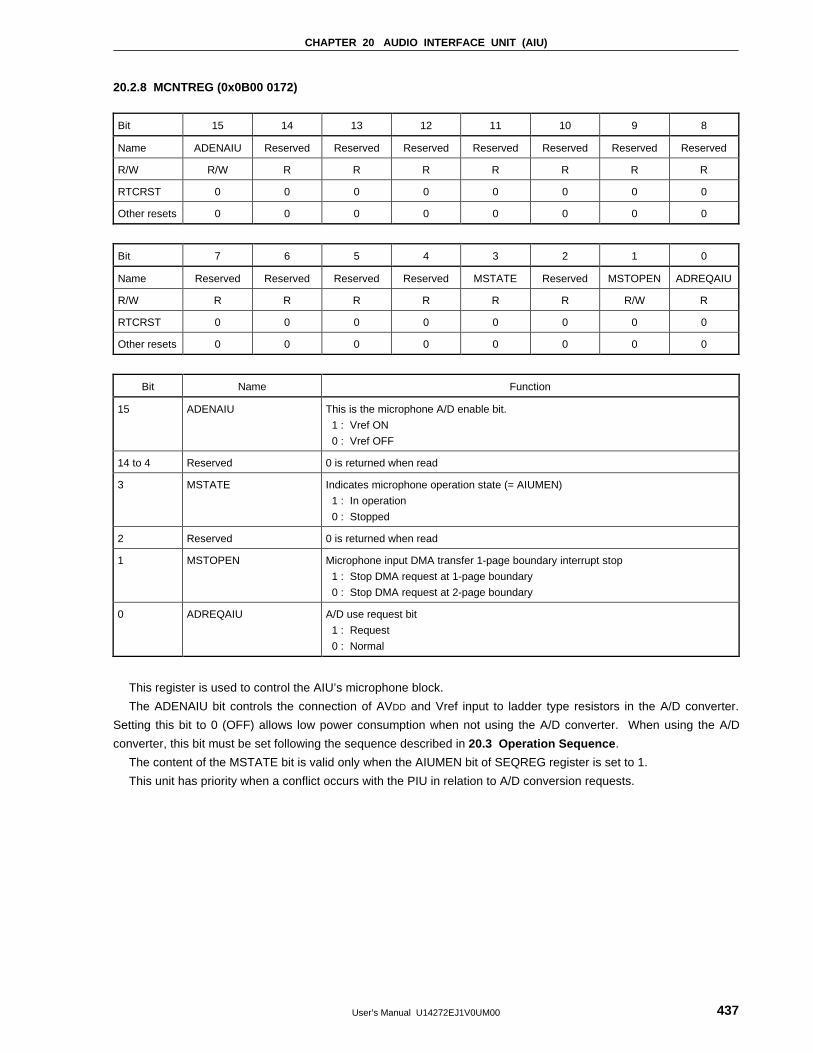
CHAPTER 20 AUDIO INTERFACE UNIT (AIU)
User’s Manual U14272EJ1V0UM00 437
20.2.8 MCNTREG (0x0B00 0172)
Bit 15 14 13 12 11 10 9 8
Name ADENAIU Reserved Reserved Reserved Reserved Reserved Reserved Reserved
R/W R/W R R R R R R R
RTCRST 0 0 0 0 0 0 0 0
Other resets 0 0 0 0 0 0 0 0
Bit 7 6 5 4 3 2 1 0
Name Reserved Reserved Reserved Reserved MSTATE Reserved MSTOPEN ADREQAIU
R/W R R R R R R R/W R
RTCRST 0 0 0 0 0 0 0 0
Other resets 0 0 0 0 0 0 0 0
Bit Name Function
15 ADENAIU This is the microphone A/D enable bit.
1 : Vref ON
0 : Vref OFF
14 to 4 Reserved 0 is returned when read
3 MSTATE Indicates microphone operation state (= AIUMEN)
1 : In operation
0 : Stopped
2 Reserved 0 is returned when read
1 MSTOPEN Microphone input DMA transfer 1-page boundary interrupt stop
1 : Stop DMA request at 1-page boundary
0 : Stop DMA request at 2-page boundary
0 ADREQAIU A/D use request bit
1 : Request
0 : Normal
This register is used to control the AIU’s microphone block.
The ADENAIU bit controls the connection of AVDD and Vref input to ladder type resistors in the A/D converter.
Setting this bit to 0 (OFF) allows low power consumption when not using the A/D converter. When using the A/D
converter, this bit must be set following the sequence described in 20.3 Operation Sequence .
The content of the MSTATE bit is valid only when the AIUMEN bit of SEQREG register is set to 1.
This unit has priority when a conflict occurs with the PIU in relation to A/D conversion requests.
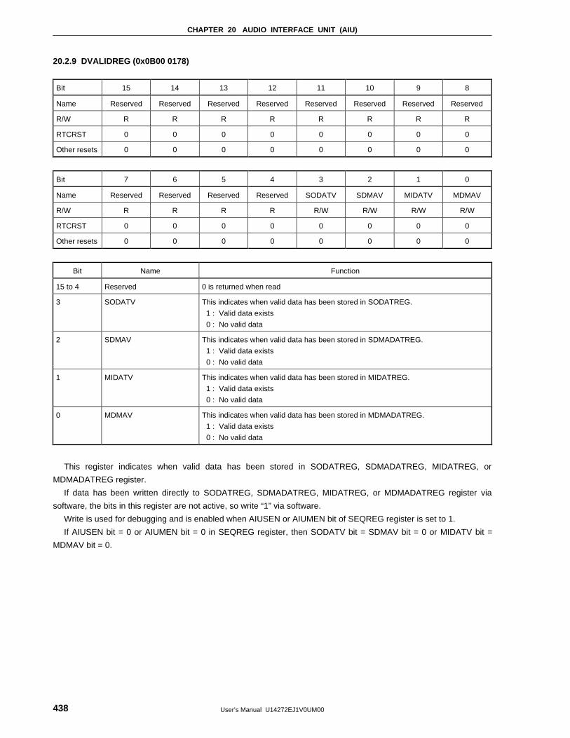
CHAPTER 20 AUDIO INTERFACE UNIT (AIU)
User’s Manual U14272EJ1V0UM00438
20.2.9 DVALIDREG (0x0B00 0178)
Bit 15 14 13 12 11 10 9 8
Name Reserved Reserved Reserved Reserved Reserved Reserved Reserved Reserved
R/W R R R R R R R R
RTCRST 0 0 0 0 0 0 0 0
Other resets 0 0 0 0 0 0 0 0
Bit 7 6 5 4 3 2 1 0
Name Reserved Reserved Reserved Reserved SODATV SDMAV MIDATV MDMAV
R/W R R R R R/W R/W R/W R/W
RTCRST 0 0 0 0 0 0 0 0
Other resets 0 0 0 0 0 0 0 0
Bit Name Function
15 to 4 Reserved 0 is returned when read
3 SODATV This indicates when valid data has been stored in SODATREG.
1 : Valid data exists
0 : No valid data
2 SDMAV This indicates when valid data has been stored in SDMADATREG.
1 : Valid data exists
0 : No valid data
1 MIDATV This indicates when valid data has been stored in MIDATREG.
1 : Valid data exists
0 : No valid data
0 MDMAV This indicates when valid data has been stored in MDMADATREG.
1 : Valid data exists
0 : No valid data
This register indicates when valid data has been stored in SODATREG, SDMADATREG, MIDATREG, or
MDMADATREG register.
If data has been written directly to SODATREG, SDMADATREG, MIDATREG, or MDMADATREG register via
software, the bits in this register are not active, so write “1” via software.
Write is used for debugging and is enabled when AIUSEN or AIUMEN bit of SEQREG register is set to 1.
If AIUSEN bit = 0 or AIUMEN bit = 0 in SEQREG register, then SODATV bit = SDMAV bit = 0 or MIDATV bit =
MDMAV bit = 0.
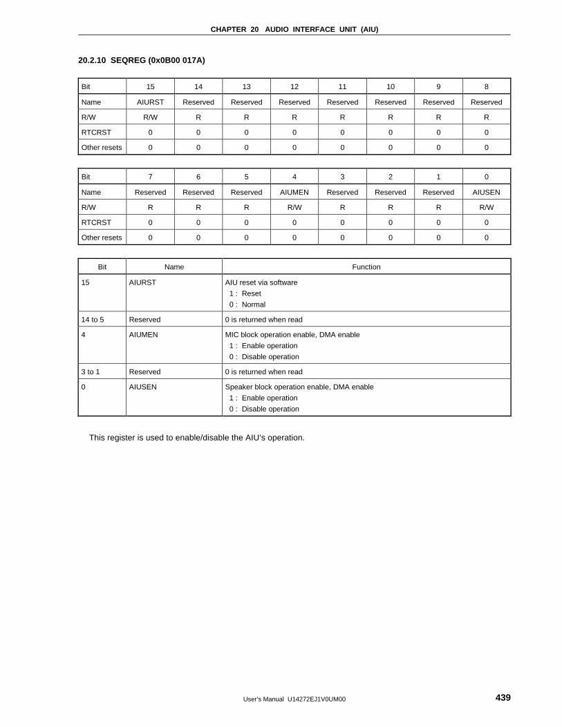
CHAPTER 20 AUDIO INTERFACE UNIT (AIU)
User’s Manual U14272EJ1V0UM00 439
20.2.10 SEQREG (0x0B00 017A)
Bit 15 14 13 12 11 10 9 8
Name AIURST Reserved Reserved Reserved Reserved Reserved Reserved Reserved
R/W R/W R R R R R R R
RTCRST 0 0 0 0 0 0 0 0
Other resets 0 0 0 0 0 0 0 0
Bit 7 6 5 4 3 2 1 0
Name Reserved Reserved Reserved AIUMEN Reserved Reserved Reserved AIUSEN
R/W R R R R/W R R R R/W
RTCRST 0 0 0 0 0 0 0 0
Other resets 0 0 0 0 0 0 0 0
Bit Name Function
15 AIURST AIU reset via software
1 : Reset
0 : Normal
14 to 5 Reserved 0 is returned when read
4 AIUMEN MIC block operation enable, DMA enable
1 : Enable operation
0 : Disable operation
3 to 1 Reserved 0 is returned when read
0 AIUSEN Speaker block operation enable, DMA enable
1 : Enable operation
0 : Disable operation
This register is used to enable/disable the AIU’s operation.
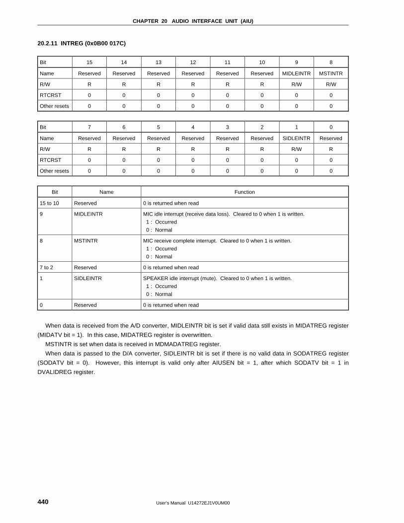
CHAPTER 20 AUDIO INTERFACE UNIT (AIU)
User’s Manual U14272EJ1V0UM00440
20.2.11 INTREG (0x0B00 017C)
Bit 15 14 13 12 11 10 9 8
Name Reserved Reserved Reserved Reserved Reserved Reserved MIDLEINTR MSTINTR
R/W R R R R R R R/W R/W
RTCRST 0 0 0 0 0 0 0 0
Other resets 0 0 0 0 0 0 0 0
Bit 7 6 5 4 3 2 1 0
Name Reserved Reserved Reserved Reserved Reserved Reserved SIDLEINTR Reserved
R/W R R R R R R R/W R
RTCRST 0 0 0 0 0 0 0 0
Other resets 0 0 0 0 0 0 0 0
Bit Name Function
15 to 10 Reserved 0 is returned when read
9 MIDLEINTR MIC idle interrupt (receive data loss). Cleared to 0 when 1 is written.
1 : Occurred
0 : Normal
8 MSTINTR MIC receive complete interrupt. Cleared to 0 when 1 is written.
1 : Occurred
0 : Normal
7 to 2 Reserved 0 is returned when read
1 SIDLEINTR SPEAKER idle interrupt (mute). Cleared to 0 when 1 is written.
1 : Occurred
0 : Normal
0 Reserved 0 is returned when read
When data is received from the A/D converter, MIDLEINTR bit is set if valid data still exists in MIDATREG register
(MIDATV bit = 1). In this case, MIDATREG register is overwritten.
MSTINTR is set when data is received in MDMADATREG register.
When data is passed to the D/A converter, SIDLEINTR bit is set if there is no valid data in SODATREG register
(SODATV bit = 0). However, this interrupt is valid only after AIUSEN bit = 1, after which SODATV bit = 1 in
DVALIDREG register.
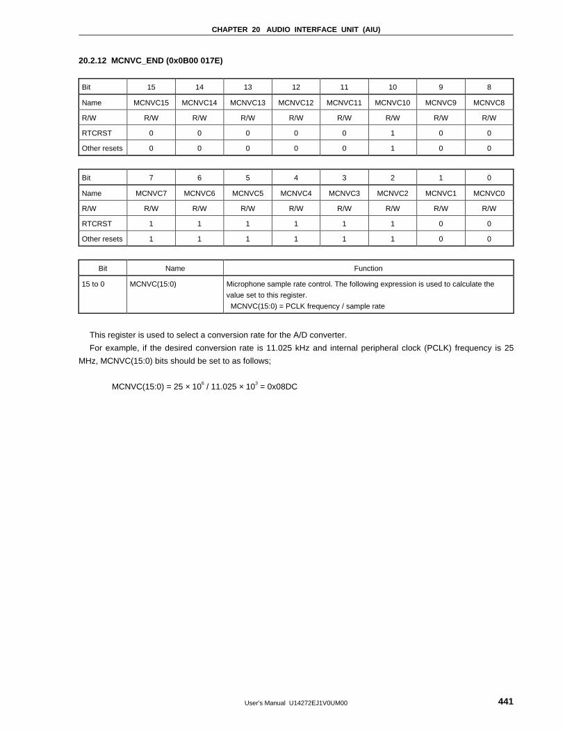
CHAPTER 20 AUDIO INTERFACE UNIT (AIU)
User’s Manual U14272EJ1V0UM00 441
20.2.12 MCNVC_END (0x0B00 017E)
Bit 15 14 13 12 11 10 9 8
Name MCNVC15 MCNVC14 MCNVC13 MCNVC12 MCNVC11 MCNVC10 MCNVC9 MCNVC8
R/W R/W R/W R/W R/W R/W R/W R/W R/W
RTCRST 0 0 0 0 0 1 0 0
Other resets 0 0 0 0 0 1 0 0
Bit 7 6 5 4 3 2 1 0
Name MCNVC7 MCNVC6 MCNVC5 MCNVC4 MCNVC3 MCNVC2 MCNVC1 MCNVC0
R/W R/W R/W R/W R/W R/W R/W R/W R/W
RTCRST 1 1 1 1 1 1 0 0
Other resets 1 1 1 1 1 1 0 0
Bit Name Function
15 to 0 MCNVC(15:0) Microphone sample rate control. The following expression is used to calculate the
value set to this register.
MCNVC(15:0) = PCLK frequency / sample rate
This register is used to select a conversion rate for the A/D converter.
For example, if the desired conversion rate is 11.025 kHz and internal peripheral clock (PCLK) frequency is 25
MHz, MCNVC(15:0) bits should be set to as follows;
MCNVC(15:0) = 25 × 106 / 11.025 × 103 = 0x08DC
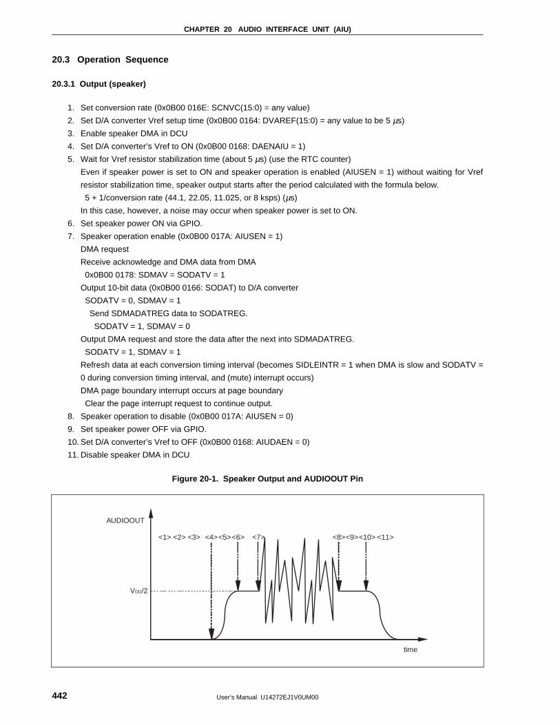
CHAPTER 20 AUDIO INTERFACE UNIT (AIU)
User’s Manual U14272EJ1V0UM00442
20.3 Operation Sequence
20.3.1 Output (speaker)
1. Set conversion rate (0x0B00 016E: SCNVC(15:0) = any value)
2. Set D/A converter Vref setup time (0x0B00 0164: DVAREF(15:0) = any value to be 5 µs)
3. Enable speaker DMA in DCU
4. Set D/A converter’s Vref to ON (0x0B00 0168: DAENAIU = 1)
5. Wait for Vref resistor stabilization time (about 5 µs) (use the RTC counter)
Even if speaker power is set to ON and speaker operation is enabled (AIUSEN = 1) without waiting for Vref
resistor stabilization time, speaker output starts after the period calculated with the formula below.
5 + 1/conversion rate (44.1, 22.05, 11.025, or 8 ksps) (µs)
In this case, however, a noise may occur when speaker power is set to ON.
6. Set speaker power ON via GPIO.
7. Speaker operation enable (0x0B00 017A: AIUSEN = 1)
DMA request
Receive acknowledge and DMA data from DMA
0x0B00 0178: SDMAV = SODATV = 1
Output 10-bit data (0x0B00 0166: SODAT) to D/A converter
SODATV = 0, SDMAV = 1
Send SDMADATREG data to SODATREG.
SODATV = 1, SDMAV = 0
Output DMA request and store the data after the next into SDMADATREG.
SODATV = 1, SDMAV = 1
Refresh data at each conversion timing interval (becomes SIDLEINTR = 1 when DMA is slow and SODATV =
0 during conversion timing interval, and (mute) interrupt occurs)
DMA page boundary interrupt occurs at page boundary
Clear the page interrupt request to continue output.
8. Speaker operation to disable (0x0B00 017A: AIUSEN = 0)
9. Set speaker power OFF via GPIO.
10. Set D/A converter’s Vref to OFF (0x0B00 0168: AIUDAEN = 0)
11. Disable speaker DMA in DCU
Figure 20-1. Speaker Output and AUDIOOUT Pin
AUDIOOUT
VDD/2
time
<1> <2> <3> <4><5><6> <7> <8><9><10> <11>
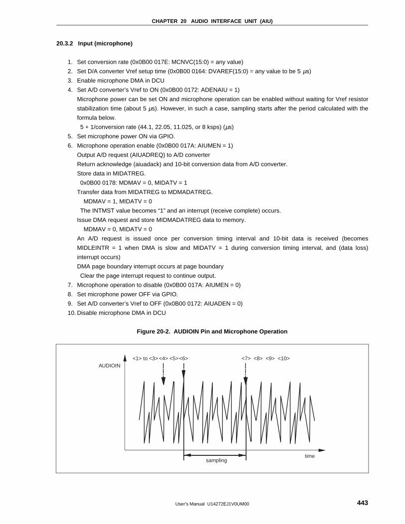
CHAPTER 20 AUDIO INTERFACE UNIT (AIU)
User’s Manual U14272EJ1V0UM00 443
20.3.2 Input (microphone)
1. Set conversion rate (0x0B00 017E: MCNVC(15:0) = any value)
2. Set D/A converter Vref setup time (0x0B00 0164: DVAREF(15:0) = any value to be 5 µs)
3. Enable microphone DMA in DCU
4. Set A/D converter’s Vref to ON (0x0B00 0172: ADENAIU = 1)
Microphone power can be set ON and microphone operation can be enabled without waiting for Vref resistor
stabilization time (about 5 µs). However, in such a case, sampling starts after the period calculated with the
formula below.
5 + 1/conversion rate (44.1, 22.05, 11.025, or 8 ksps) (µs)
5. Set microphone power ON via GPIO.
6. Microphone operation enable (0x0B00 017A: AIUMEN = 1)
Output A/D request (AIUADREQ) to A/D converter
Return acknowledge (aiuadack) and 10-bit conversion data from A/D converter.
Store data in MIDATREG.
0x0B00 0178: MDMAV = 0, MIDATV = 1
Transfer data from MIDATREG to MDMADATREG.
MDMAV = 1, MIDATV = 0
The INTMST value becomes “1” and an interrupt (receive complete) occurs.
Issue DMA request and store MIDMADATREG data to memory.
MDMAV = 0, MIDATV = 0
An A/D request is issued once per conversion timing interval and 10-bit data is received (becomes
MIDLEINTR = 1 when DMA is slow and MIDATV = 1 during conversion timing interval, and (data loss)
interrupt occurs)
DMA page boundary interrupt occurs at page boundary
Clear the page interrupt request to continue output.
7. Microphone operation to disable (0x0B00 017A: AIUMEN = 0)
8. Set microphone power OFF via GPIO.
9. Set A/D converter’s Vref to OFF (0x0B00 0172: AIUADEN = 0)
10. Disable microphone DMA in DCU
Figure 20-2. AUDIOIN Pin and Microphone Operation
AUDIOIN
sampling
<1> to <3> <4> <5><6> <7> <8> <9> <10>
time

User’s Manual U14272EJ1V0UM00444
[[[[MEMO]]]]
User’s Manual U14272EJ1V0UM00 445
CHAPTER 21 KEYBOARD INTERFACE UNIT (KIU)
21.1 General
The Keyboard Interface Unit (KIU) provides the interface between the VR4181 and an external matrix type
keyboard. This unit supports key matrix of 8 x 8.
The interface to the keyboard consists of SCANOUT and SCANIN lines. The SCANOUT lines are used to search
the matrix for pressed keys. The SCANIN lines are used to sense key press events and are read after each
SCANOUT line activation to locate the pressed key.
SCANOUT and SCANIN lines are allocated by programming VR4181 CompactFlash pins to support this function.
These pins are multiplexed. Only one configuration is set by the firmware during the power-on. SCANOUT lines are
defined as 3-state outputs and SCANIN lines are inputs.
21.2 Functional Description
When the keyboard is idle, the SCANOUT lines are all driven to 0 volts and the SCANIN lines are pulled to VDD by
external 4.7 kΩ resistors. When any key in the matrix is pressed, at least one SCANIN input will be driven low and
signals a key press event to the KIU.
Once the key press event has been detected, the KIU may be programmed to generate a Key Input Detection
interrupt request and automatically begin scanning the keyboard or wait until software enables the scan operation.
Keyboard scanning is performed by sequentially driving one SCANOUT line low while the others remain 3-state
and reading the state of the SCANIN lines into keyboard data registers inside the KIU. Once the last SCANOUT line
has been driven low and the SCANIN lines read the KIU may generate a Keyboard Data Ready interrupt request to
inform system software that one keyboard scan operation has been completed.
The KIU repeats this scan process until no further keys have been detected or until software disables the scan
operation. At this point the KIU returns to the keyboard idle state and waits for the next key press event.
21.2.1 Automatic keyboard scan mode
Automatic Scan mode is enabled through the ATSCAN and ATSTP bits of the KIUSCANREP register. When the
ATSCAN bit is set to 1, keyboard scanning starts automatically following a Key Detect Interrupt request. When the
ATSTP bit is set to 1, keyboard scanning stops automatically after no valid keyboard data (i.e. all SCANIN lines are
high level) has been read for the number of scan cycles specified by the STPREP(5:0) bits of the KIUSCANREP
register.
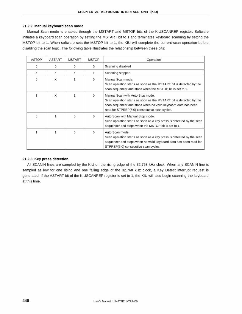
CHAPTER 21 KEYBOARD INTERFACE UNIT (KIU)
User’s Manual U14272EJ1V0UM00446
21.2.2 Manual keyboard scan mode
Manual Scan mode is enabled through the MSTART and MSTOP bits of the KIUSCANREP register. Software
initiates a keyboard scan operation by setting the MSTART bit to 1 and terminates keyboard scanning by setting the
MSTOP bit to 1. When software sets the MSTOP bit to 1, the KIU will complete the current scan operation before
disabling the scan logic. The following table illustrates the relationship between these bits:
ASTOP ASTART MSTART MSTOP Operation
0 0 0 0 Scanning disabled
X X X 1 Scanning stopped
0 X 1 0 Manual Scan mode.
Scan operation starts as soon as the MSTART bit is detected by the
scan sequencer and stops when the MSTOP bit is set to 1.
1 X 1 0 Manual Scan with Auto Stop mode.
Scan operation starts as soon as the MSTART bit is detected by the
scan sequencer and stops when no valid keyboard data has been
read for STPREP(5:0) consecutive scan cycles.
0 1 0 0 Auto Scan with Manual Stop mode.
Scan operation starts as soon as a key press is detected by the scan
sequencer and stops when the MSTOP bit is set to 1.
1 1 0 0 Auto Scan mode.
Scan operation starts as soon as a key press is detected by the scan
sequencer and stops when no valid keyboard data has been read for
STPREP(5:0) consecutive scan cycles.
21.2.3 Key press detection
All SCANIN lines are sampled by the KIU on the rising edge of the 32.768 kHz clock. When any SCANIN line is
sampled as low for one rising and one falling edge of the 32.768 kHz clock, a Key Detect interrupt request is
generated. If the ASTART bit of the KIUSCANREP register is set to 1, the KIU will also begin scanning the keyboard
at this time.
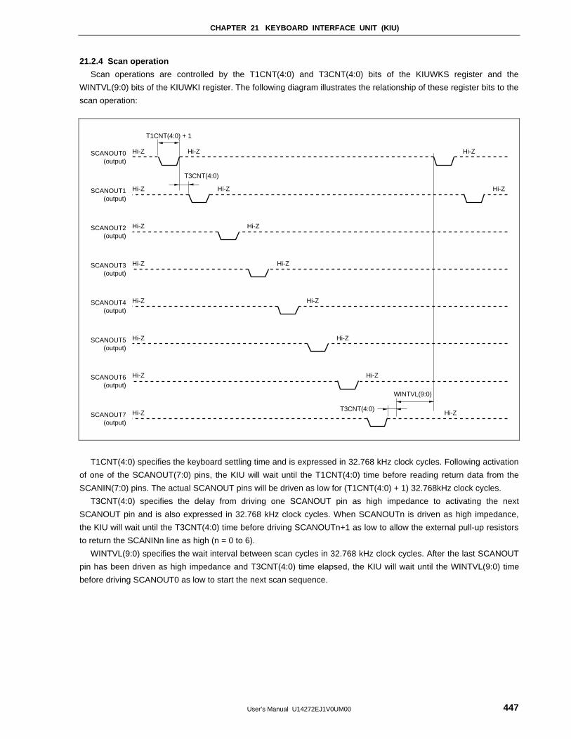
CHAPTER 21 KEYBOARD INTERFACE UNIT (KIU)
User’s Manual U14272EJ1V0UM00 447
21.2.4 Scan operation
Scan operations are controlled by the T1CNT(4:0) and T3CNT(4:0) bits of the KIUWKS register and the
WINTVL(9:0) bits of the KIUWKI register. The following diagram illustrates the relationship of these register bits to the
scan operation:
T1CNT(4:0) + 1
T3CNT(4:0)
SCANOUT0(output)
Hi-Z Hi-Z
SCANOUT1(output)
Hi-Z Hi-Z
SCANOUT2(output)
Hi-Z Hi-Z
SCANOUT3(output)
Hi-Z Hi-Z
SCANOUT4(output)
Hi-Z Hi-Z
SCANOUT5(output)
Hi-Z Hi-Z
T3CNT(4:0)
WINTVL(9:0)
SCANOUT6(output)
Hi-Z Hi-Z
SCANOUT7(output)
Hi-Z Hi-Z
Hi-Z
Hi-Z
T1CNT(4:0) specifies the keyboard settling time and is expressed in 32.768 kHz clock cycles. Following activation
of one of the SCANOUT(7:0) pins, the KIU will wait until the T1CNT(4:0) time before reading return data from the
SCANIN(7:0) pins. The actual SCANOUT pins will be driven as low for (T1CNT(4:0) + 1) 32.768kHz clock cycles.
T3CNT(4:0) specifies the delay from driving one SCANOUT pin as high impedance to activating the next
SCANOUT pin and is also expressed in 32.768 kHz clock cycles. When SCANOUTn is driven as high impedance,
the KIU will wait until the T3CNT(4:0) time before driving SCANOUTn+1 as low to allow the external pull-up resistors
to return the SCANINn line as high (n = 0 to 6).
WINTVL(9:0) specifies the wait interval between scan cycles in 32.768 kHz clock cycles. After the last SCANOUT
pin has been driven as high impedance and T3CNT(4:0) time elapsed, the KIU will wait until the WINTVL(9:0) time
before driving SCANOUT0 as low to start the next scan sequence.
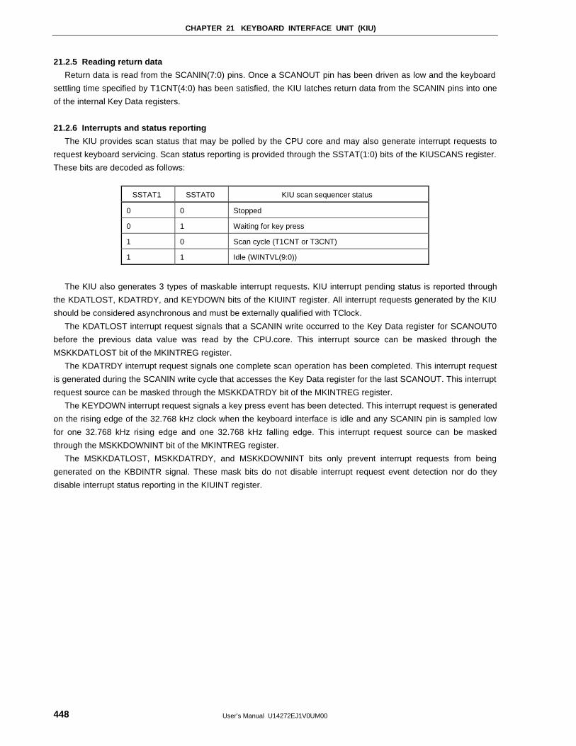
CHAPTER 21 KEYBOARD INTERFACE UNIT (KIU)
User’s Manual U14272EJ1V0UM00448
21.2.5 Reading return data
Return data is read from the SCANIN(7:0) pins. Once a SCANOUT pin has been driven as low and the keyboard
settling time specified by T1CNT(4:0) has been satisfied, the KIU latches return data from the SCANIN pins into one
of the internal Key Data registers.
21.2.6 Interrupts and status reporting
The KIU provides scan status that may be polled by the CPU core and may also generate interrupt requests to
request keyboard servicing. Scan status reporting is provided through the SSTAT(1:0) bits of the KIUSCANS register.
These bits are decoded as follows:
SSTAT1 SSTAT0 KIU scan sequencer status
0 0 Stopped
0 1 Waiting for key press
1 0 Scan cycle (T1CNT or T3CNT)
1 1 Idle (WINTVL(9:0))
The KIU also generates 3 types of maskable interrupt requests. KIU interrupt pending status is reported through
the KDATLOST, KDATRDY, and KEYDOWN bits of the KIUINT register. All interrupt requests generated by the KIU
should be considered asynchronous and must be externally qualified with TClock.
The KDATLOST interrupt request signals that a SCANIN write occurred to the Key Data register for SCANOUT0
before the previous data value was read by the CPU.core. This interrupt source can be masked through the
MSKKDATLOST bit of the MKINTREG register.
The KDATRDY interrupt request signals one complete scan operation has been completed. This interrupt request
is generated during the SCANIN write cycle that accesses the Key Data register for the last SCANOUT. This interrupt
request source can be masked through the MSKKDATRDY bit of the MKINTREG register.
The KEYDOWN interrupt request signals a key press event has been detected. This interrupt request is generated
on the rising edge of the 32.768 kHz clock when the keyboard interface is idle and any SCANIN pin is sampled low
for one 32.768 kHz rising edge and one 32.768 kHz falling edge. This interrupt request source can be masked
through the MSKKDOWNINT bit of the MKINTREG register.
The MSKKDATLOST, MSKKDATRDY, and MSKKDOWNINT bits only prevent interrupt requests from being
generated on the KBDINTR signal. These mask bits do not disable interrupt request event detection nor do they
disable interrupt status reporting in the KIUINT register.
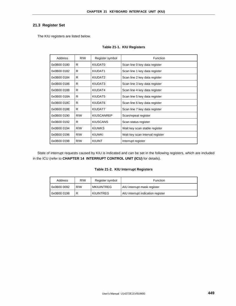
CHAPTER 21 KEYBOARD INTERFACE UNIT (KIU)
User’s Manual U14272EJ1V0UM00 449
21.3 Register Set
The KIU registers are listed below.
Table 21-1. KIU Registers
Address R/W Register symbol Function
0x0B00 0180 R KIUDAT0 Scan line 0 key data register
0x0B00 0182 R KIUDAT1 Scan line 1 key data register
0x0B00 0184 R KIUDAT2 Scan line 2 key data register
0x0B00 0186 R KIUDAT3 Scan line 3 key data register
0x0B00 0188 R KIUDAT4 Scan line 4 key data register
0x0B00 018A R KIUDAT5 Scan line 5 key data register
0x0B00 018C R KIUDAT6 Scan line 6 key data register
0x0B00 018E R KIUDAT7 Scan line 7 key data register
0x0B00 0190 R/W KIUSCANREP Scan/repeat register
0x0B00 0192 R KIUSCANS Scan status register
0x0B00 0194 R/W KIUWKS Wait key scan stable register
0x0B00 0196 R/W KIUWKI Wait key scan interval register
0x0B00 0198 R/W KIUINT Interrupt register
State of interrupt requests caused by KIU is indicated and can be set in the following registers, which are included
in the ICU (refer to CHAPTER 14 INTERRUPT CONTROL UNIT (ICU) for details).
Table 21-2. KIU Interrupt Registers
Address R/W Register symbol Function
0x0B00 0092 R/W MKIUINTREG AIU interrupt mask register
0x0B00 0198 R KIUINTREG AIU interrupt indication register
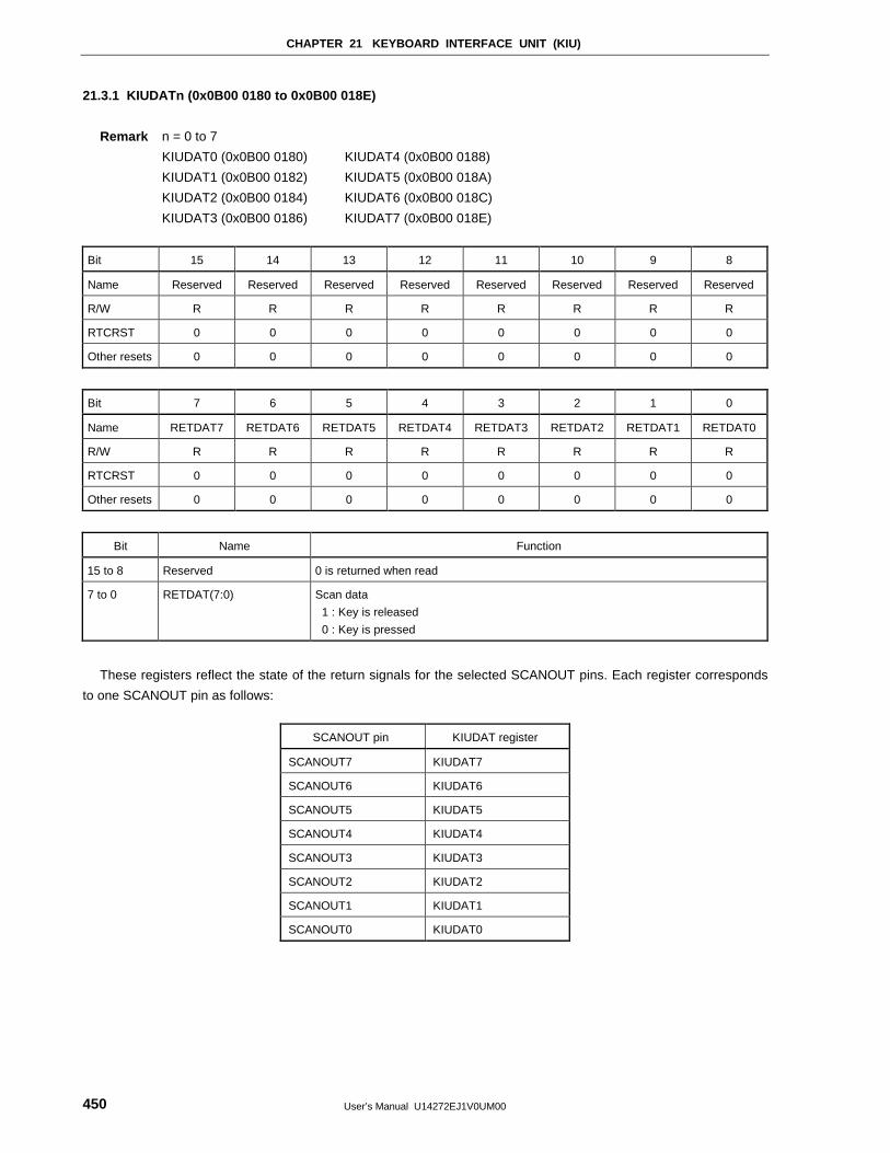
CHAPTER 21 KEYBOARD INTERFACE UNIT (KIU)
User’s Manual U14272EJ1V0UM00450
21.3.1 KIUDATn (0x0B00 0180 to 0x0B00 018E)
Remark n = 0 to 7
KIUDAT0 (0x0B00 0180) KIUDAT4 (0x0B00 0188)
KIUDAT1 (0x0B00 0182) KIUDAT5 (0x0B00 018A)
KIUDAT2 (0x0B00 0184) KIUDAT6 (0x0B00 018C)
KIUDAT3 (0x0B00 0186) KIUDAT7 (0x0B00 018E)
Bit 15 14 13 12 11 10 9 8
Name Reserved Reserved Reserved Reserved Reserved Reserved Reserved Reserved
R/W R R R R R R R R
RTCRST 0 0 0 0 0 0 0 0
Other resets 0 0 0 0 0 0 0 0
Bit 7 6 5 4 3 2 1 0
Name RETDAT7 RETDAT6 RETDAT5 RETDAT4 RETDAT3 RETDAT2 RETDAT1 RETDAT0
R/W R R R R R R R R
RTCRST 0 0 0 0 0 0 0 0
Other resets 0 0 0 0 0 0 0 0
Bit Name Function
15 to 8 Reserved 0 is returned when read
7 to 0 RETDAT(7:0) Scan data
1 : Key is released
0 : Key is pressed
These registers reflect the state of the return signals for the selected SCANOUT pins. Each register corresponds
to one SCANOUT pin as follows:
SCANOUT pin KIUDAT register
SCANOUT7 KIUDAT7
SCANOUT6 KIUDAT6
SCANOUT5 KIUDAT5
SCANOUT4 KIUDAT4
SCANOUT3 KIUDAT3
SCANOUT2 KIUDAT2
SCANOUT1 KIUDAT1
SCANOUT0 KIUDAT0
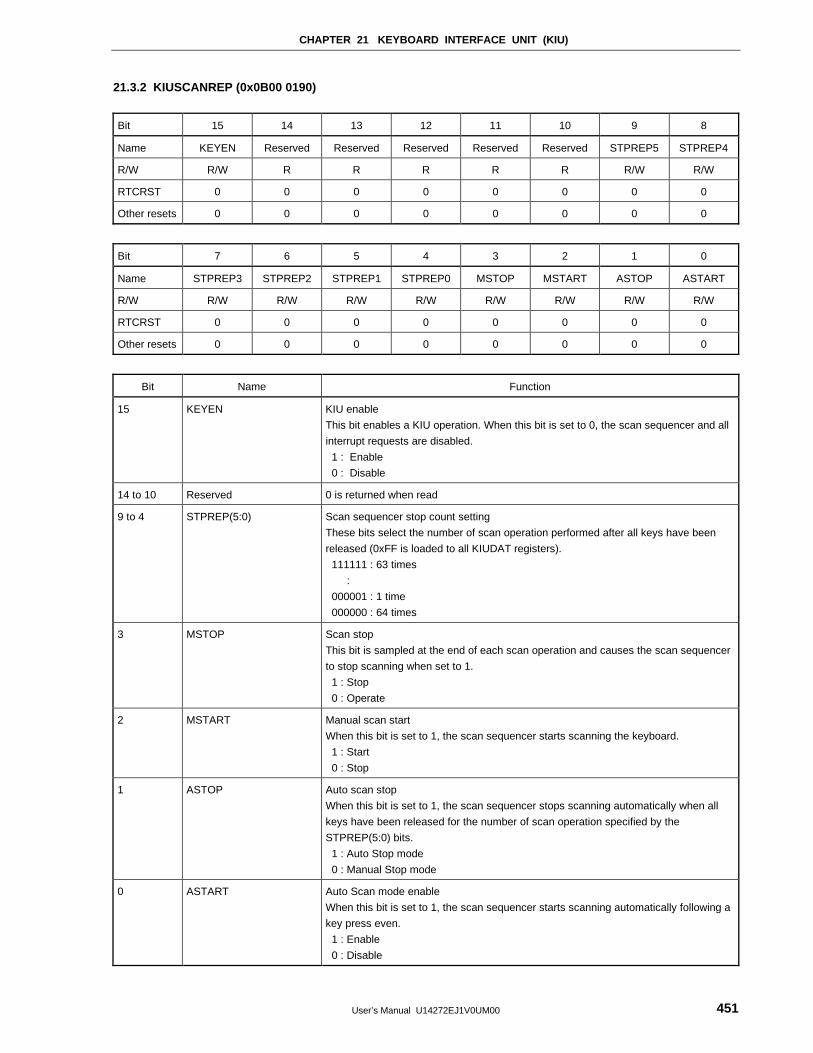
CHAPTER 21 KEYBOARD INTERFACE UNIT (KIU)
User’s Manual U14272EJ1V0UM00 451
21.3.2 KIUSCANREP (0x0B00 0190)
Bit 15 14 13 12 11 10 9 8
Name KEYEN Reserved Reserved Reserved Reserved Reserved STPREP5 STPREP4
R/W R/W R R R R R R/W R/W
RTCRST 0 0 0 0 0 0 0 0
Other resets 0 0 0 0 0 0 0 0
Bit 7 6 5 4 3 2 1 0
Name STPREP3 STPREP2 STPREP1 STPREP0 MSTOP MSTART ASTOP ASTART
R/W R/W R/W R/W R/W R/W R/W R/W R/W
RTCRST 0 0 0 0 0 0 0 0
Other resets 0 0 0 0 0 0 0 0
Bit Name Function
15 KEYEN KIU enable
This bit enables a KIU operation. When this bit is set to 0, the scan sequencer and all
interrupt requests are disabled.
1 : Enable
0 : Disable
14 to 10 Reserved 0 is returned when read
9 to 4 STPREP(5:0) Scan sequencer stop count setting
These bits select the number of scan operation performed after all keys have been
released (0xFF is loaded to all KIUDAT registers).
111111 : 63 times
:
000001 : 1 time
000000 : 64 times
3 MSTOP Scan stop
This bit is sampled at the end of each scan operation and causes the scan sequencer
to stop scanning when set to 1.
1 : Stop
0 : Operate
2 MSTART Manual scan start
When this bit is set to 1, the scan sequencer starts scanning the keyboard.
1 : Start
0 : Stop
1 ASTOP Auto scan stop
When this bit is set to 1, the scan sequencer stops scanning automatically when all
keys have been released for the number of scan operation specified by the
STPREP(5:0) bits.
1 : Auto Stop mode
0 : Manual Stop mode
0 ASTART Auto Scan mode enable
When this bit is set to 1, the scan sequencer starts scanning automatically following a
key press even.
1 : Enable
0 : Disable
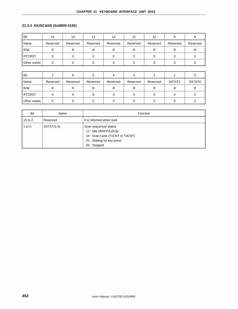
CHAPTER 21 KEYBOARD INTERFACE UNIT (KIU)
User’s Manual U14272EJ1V0UM00452
21.3.3 KIUSCANS (0x0B00 0192)
Bit 15 14 13 12 11 10 9 8
Name Reserved Reserved Reserved Reserved Reserved Reserved Reserved Reserved
R/W R R R R R R R R
RTCRST 0 0 0 0 0 0 0 0
Other resets 0 0 0 0 0 0 0 0
Bit 7 6 5 4 3 2 1 0
Name Reserved Reserved Reserved Reserved Reserved Reserved SSTAT1 SSTAT0
R/W R R R R R R R R
RTCRST 0 0 0 0 0 0 0 0
Other resets 0 0 0 0 0 0 0 0
Bit Name Function
15 to 2 Reserved 0 is returned when read
1 to 0 SSTAT(1:0) Scan sequencer status
11 : Idle (WINTVL(9:0))
10 : Scan cycle (T1CNT or T3CNT)
01 : Waiting for key press
00 : Stopped
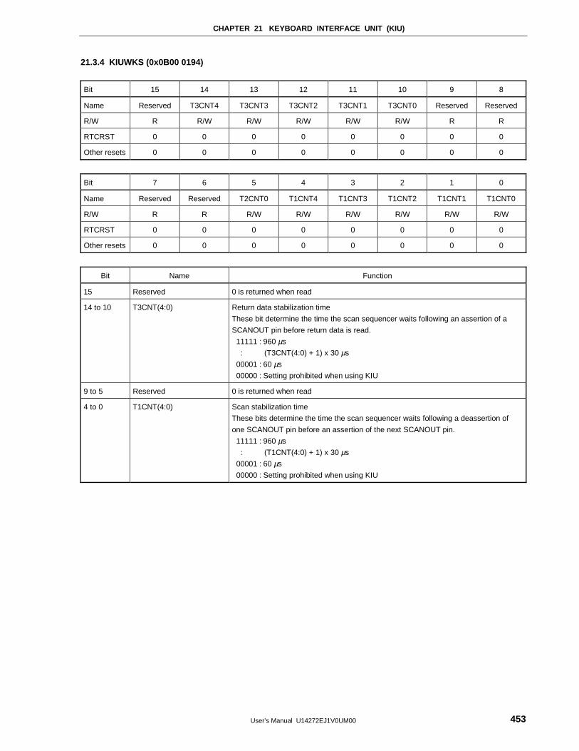
CHAPTER 21 KEYBOARD INTERFACE UNIT (KIU)
User’s Manual U14272EJ1V0UM00 453
21.3.4 KIUWKS (0x0B00 0194)
Bit 15 14 13 12 11 10 9 8
Name Reserved T3CNT4 T3CNT3 T3CNT2 T3CNT1 T3CNT0 Reserved Reserved
R/W R R/W R/W R/W R/W R/W R R
RTCRST 0 0 0 0 0 0 0 0
Other resets 0 0 0 0 0 0 0 0
Bit 7 6 5 4 3 2 1 0
Name Reserved Reserved T2CNT0 T1CNT4 T1CNT3 T1CNT2 T1CNT1 T1CNT0
R/W R R R/W R/W R/W R/W R/W R/W
RTCRST 0 0 0 0 0 0 0 0
Other resets 0 0 0 0 0 0 0 0
Bit Name Function
15 Reserved 0 is returned when read
14 to 10 T3CNT(4:0) Return data stabilization time
These bit determine the time the scan sequencer waits following an assertion of a
SCANOUT pin before return data is read.
11111 : 960 µs
: (T3CNT(4:0) + 1) x 30 µs
00001 : 60 µs
00000 : Setting prohibited when using KIU
9 to 5 Reserved 0 is returned when read
4 to 0 T1CNT(4:0) Scan stabilization time
These bits determine the time the scan sequencer waits following a deassertion of
one SCANOUT pin before an assertion of the next SCANOUT pin.
11111 : 960 µs
: (T1CNT(4:0) + 1) x 30 µs
00001 : 60 µs
00000 : Setting prohibited when using KIU
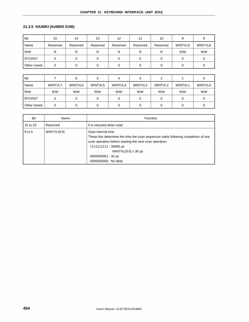
CHAPTER 21 KEYBOARD INTERFACE UNIT (KIU)
User’s Manual U14272EJ1V0UM00454
21.3.5 KIUWKI (0x0B00 0196)
Bit 15 14 13 12 11 10 9 8
Name Reserved Reserved Reserved Reserved Reserved Reserved WINTVL9 WINTVL8
R/W R R R R R R R/W R/W
RTCRST 0 0 0 0 0 0 0 0
Other resets 0 0 0 0 0 0 0 0
Bit 7 6 5 4 3 2 1 0
Name WINTVL7 WINTVL6 WINTVL5 WINTVL4 WINTVL3 WINTVL2 WINTVL1 WINTVL0
R/W R/W R/W R/W R/W R/W R/W R/W R/W
RTCRST 0 0 0 0 0 0 0 0
Other resets 0 0 0 0 0 0 0 0
Bit Name Function
15 to 10 Reserved 0 is returned when read
9 to 0 WINTVL(9:0) Scan interval time
These bits determine the time the scan sequencer waits following completion of one
scan operation before starting the next scan operation.
1111111111 : 30690 µs
: WINTVL(9:0) x 30 µs
0000000001 : 30 µs
0000000000 : No Wait
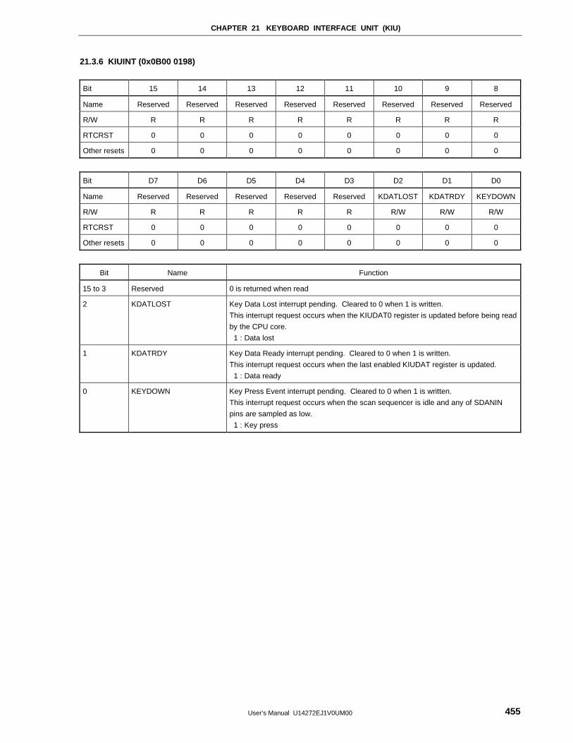
CHAPTER 21 KEYBOARD INTERFACE UNIT (KIU)
User’s Manual U14272EJ1V0UM00 455
21.3.6 KIUINT (0x0B00 0198)
Bit 15 14 13 12 11 10 9 8
Name Reserved Reserved Reserved Reserved Reserved Reserved Reserved Reserved
R/W R R R R R R R R
RTCRST 0 0 0 0 0 0 0 0
Other resets 0 0 0 0 0 0 0 0
Bit D7 D6 D5 D4 D3 D2 D1 D0
Name Reserved Reserved Reserved Reserved Reserved KDATLOST KDATRDY KEYDOWN
R/W R R R R R R/W R/W R/W
RTCRST 0 0 0 0 0 0 0 0
Other resets 0 0 0 0 0 0 0 0
Bit Name Function
15 to 3 Reserved 0 is returned when read
2 KDATLOST Key Data Lost interrupt pending. Cleared to 0 when 1 is written.
This interrupt request occurs when the KIUDAT0 register is updated before being read
by the CPU core.
1 : Data lost
1 KDATRDY Key Data Ready interrupt pending. Cleared to 0 when 1 is written.
This interrupt request occurs when the last enabled KIUDAT register is updated.
1 : Data ready
0 KEYDOWN Key Press Event interrupt pending. Cleared to 0 when 1 is written.
This interrupt request occurs when the scan sequencer is idle and any of SDANIN
pins are sampled as low.
1 : Key press

User’s Manual U14272EJ1V0UM00456
[MEMO]
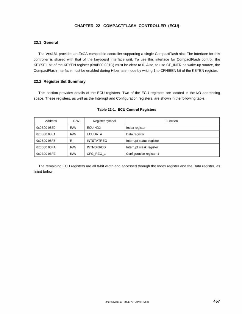
User’s Manual U14272EJ1V0UM00 457
CHAPTER 22 COMPACTFLASH CONTROLLER (ECU)
22.1 General
The VR4181 provides an ExCA-compatible controller supporting a single CompactFlash slot. The interface for this
controller is shared with that of the keyboard interface unit. To use this interface for CompactFlash control, the
KEYSEL bit of the KEYEN register (0x0B00 031C) must be clear to 0. Also, to use CF_INTR as wake-up source, the
CompactFlash interface must be enabled during Hibernate mode by writing 1 to CFHIBEN bit of the KEYEN register.
22.2 Register Set Summary
This section provides details of the ECU registers. Two of the ECU registers are located in the I/O addressing
space. These registers, as well as the Interrupt and Configuration registers, are shown in the following table.
Table 22-1. ECU Control Registers
Address R/W Register symbol Function
0x0B00 08E0 R/W ECUINDX Index register
0x0B00 08E1 R/W ECUDATA Data register
0x0B00 08F8 R INTSTATREG Interrupt status register
0x0B00 08FA R/W INTMSKREG Interrupt mask register
0x0B00 08FE R/W CFG_REG_1 Configuration register 1
The remaining ECU registers are all 8-bit width and accessed through the Index register and the Data register, as
listed below.
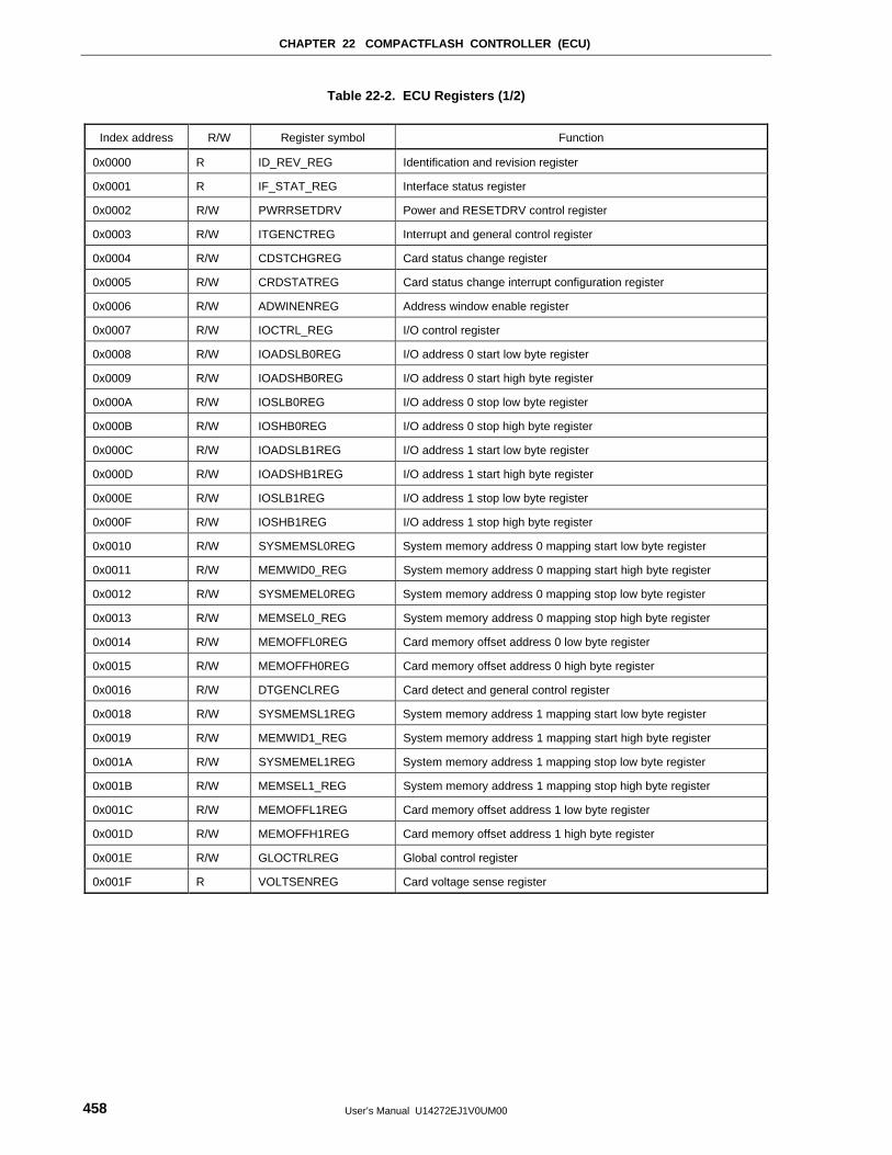
CHAPTER 22 COMPACTFLASH CONTROLLER (ECU)
User’s Manual U14272EJ1V0UM00458
Table 22-2. ECU Registers (1/2)
Index address R/W Register symbol Function
0x0000 R ID_REV_REG Identification and revision register
0x0001 R IF_STAT_REG Interface status register
0x0002 R/W PWRRSETDRV Power and RESETDRV control register
0x0003 R/W ITGENCTREG Interrupt and general control register
0x0004 R/W CDSTCHGREG Card status change register
0x0005 R/W CRDSTATREG Card status change interrupt configuration register
0x0006 R/W ADWINENREG Address window enable register
0x0007 R/W IOCTRL_REG I/O control register
0x0008 R/W IOADSLB0REG I/O address 0 start low byte register
0x0009 R/W IOADSHB0REG I/O address 0 start high byte register
0x000A R/W IOSLB0REG I/O address 0 stop low byte register
0x000B R/W IOSHB0REG I/O address 0 stop high byte register
0x000C R/W IOADSLB1REG I/O address 1 start low byte register
0x000D R/W IOADSHB1REG I/O address 1 start high byte register
0x000E R/W IOSLB1REG I/O address 1 stop low byte register
0x000F R/W IOSHB1REG I/O address 1 stop high byte register
0x0010 R/W SYSMEMSL0REG System memory address 0 mapping start low byte register
0x0011 R/W MEMWID0_REG System memory address 0 mapping start high byte register
0x0012 R/W SYSMEMEL0REG System memory address 0 mapping stop low byte register
0x0013 R/W MEMSEL0_REG System memory address 0 mapping stop high byte register
0x0014 R/W MEMOFFL0REG Card memory offset address 0 low byte register
0x0015 R/W MEMOFFH0REG Card memory offset address 0 high byte register
0x0016 R/W DTGENCLREG Card detect and general control register
0x0018 R/W SYSMEMSL1REG System memory address 1 mapping start low byte register
0x0019 R/W MEMWID1_REG System memory address 1 mapping start high byte register
0x001A R/W SYSMEMEL1REG System memory address 1 mapping stop low byte register
0x001B R/W MEMSEL1_REG System memory address 1 mapping stop high byte register
0x001C R/W MEMOFFL1REG Card memory offset address 1 low byte register
0x001D R/W MEMOFFH1REG Card memory offset address 1 high byte register
0x001E R/W GLOCTRLREG Global control register
0x001F R VOLTSENREG Card voltage sense register
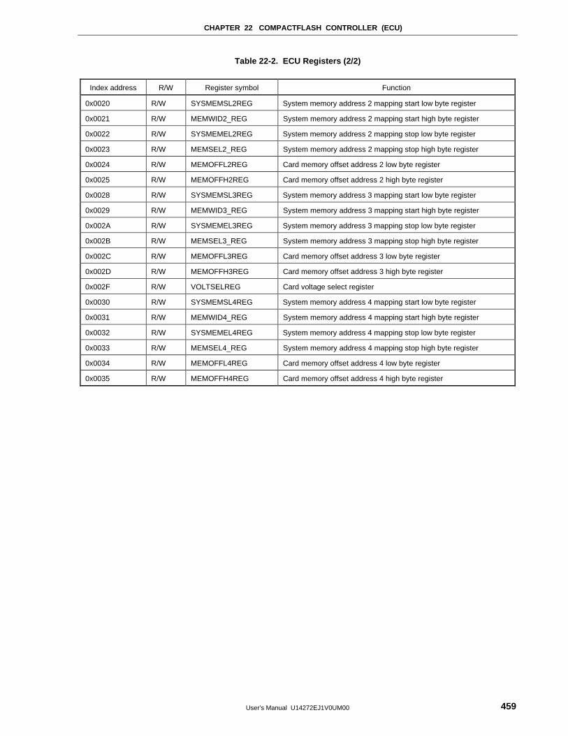
CHAPTER 22 COMPACTFLASH CONTROLLER (ECU)
User’s Manual U14272EJ1V0UM00 459
Table 22-2. ECU Registers (2/2)
Index address R/W Register symbol Function
0x0020 R/W SYSMEMSL2REG System memory address 2 mapping start low byte register
0x0021 R/W MEMWID2_REG System memory address 2 mapping start high byte register
0x0022 R/W SYSMEMEL2REG System memory address 2 mapping stop low byte register
0x0023 R/W MEMSEL2_REG System memory address 2 mapping stop high byte register
0x0024 R/W MEMOFFL2REG Card memory offset address 2 low byte register
0x0025 R/W MEMOFFH2REG Card memory offset address 2 high byte register
0x0028 R/W SYSMEMSL3REG System memory address 3 mapping start low byte register
0x0029 R/W MEMWID3_REG System memory address 3 mapping start high byte register
0x002A R/W SYSMEMEL3REG System memory address 3 mapping stop low byte register
0x002B R/W MEMSEL3_REG System memory address 3 mapping stop high byte register
0x002C R/W MEMOFFL3REG Card memory offset address 3 low byte register
0x002D R/W MEMOFFH3REG Card memory offset address 3 high byte register
0x002F R/W VOLTSELREG Card voltage select register
0x0030 R/W SYSMEMSL4REG System memory address 4 mapping start low byte register
0x0031 R/W MEMWID4_REG System memory address 4 mapping start high byte register
0x0032 R/W SYSMEMEL4REG System memory address 4 mapping stop low byte register
0x0033 R/W MEMSEL4_REG System memory address 4 mapping stop high byte register
0x0034 R/W MEMOFFL4REG Card memory offset address 4 low byte register
0x0035 R/W MEMOFFH4REG Card memory offset address 4 high byte register
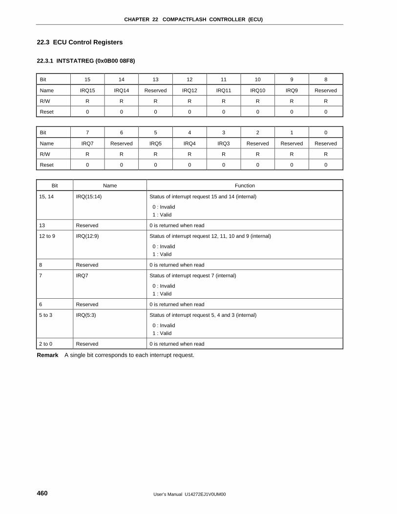
CHAPTER 22 COMPACTFLASH CONTROLLER (ECU)
User’s Manual U14272EJ1V0UM00460
22.3 ECU Control Registers
22.3.1 INTSTATREG (0x0B00 08F8)
Bit 15 14 13 12 11 10 9 8
Name IRQ15 IRQ14 Reserved IRQ12 IRQ11 IRQ10 IRQ9 Reserved
R/W R R R R R R R R
Reset 0 0 0 0 0 0 0 0
Bit 7 6 5 4 3 2 1 0
Name IRQ7 Reserved IRQ5 IRQ4 IRQ3 Reserved Reserved Reserved
R/W R R R R R R R R
Reset 0 0 0 0 0 0 0 0
Bit Name Function
15, 14 IRQ(15:14) Status of interrupt request 15 and 14 (internal)
0 : Invalid
1 : Valid
13 Reserved 0 is returned when read
12 to 9 IRQ(12:9) Status of interrupt request 12, 11, 10 and 9 (internal)
0 : Invalid
1 : Valid
8 Reserved 0 is returned when read
7 IRQ7 Status of interrupt request 7 (internal)
0 : Invalid
1 : Valid
6 Reserved 0 is returned when read
5 to 3 IRQ(5:3) Status of interrupt request 5, 4 and 3 (internal)
0 : Invalid
1 : Valid
2 to 0 Reserved 0 is returned when read
Remark A single bit corresponds to each interrupt request.
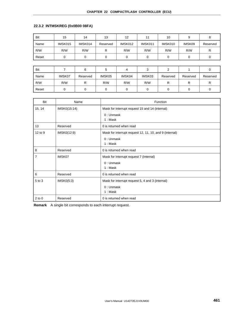
CHAPTER 22 COMPACTFLASH CONTROLLER (ECU)
User’s Manual U14272EJ1V0UM00 461
22.3.2 INTMSKREG (0x0B00 08FA)
Bit 15 14 13 12 11 10 9 8
Name IMSK015 IMSK014 Reserved IMSK012 IMSK011 IMSK010 IMSK09 Reserved
R/W R/W R/W R R/W R/W R/W R/W R
Reset 0 0 0 0 0 0 0 0
Bit 7 6 5 4 3 2 1 0
Name IMSK07 Reserved IMSK05 IMSK04 IMSK03 Reserved Reserved Reserved
R/W R/W R R/W R/W R/W R R R
Reset 0 0 0 0 0 0 0 0
Bit Name Function
15, 14 IMSK0(15:14) Mask for interrupt request 15 and 14 (internal)
0 : Unmask
1 : Mask
13 Reserved 0 is returned when read
12 to 9 IMSK0(12:9) Mask for interrupt request 12, 11, 10, and 9 (internal)
0 : Unmask
1 : Mask
8 Reserved 0 is returned when read
7 IMSK07 Mask for interrupt request 7 (internal)
0 : Unmask
1 : Mask
6 Reserved 0 is returned when read
5 to 3 IMSK0(5:3) Mask for interrupt request 5, 4 and 3 (internal)
0 : Unmask
1 : Mask
2 to 0 Reserved 0 is returned when read
Remark A single bit corresponds to each interrupt request.
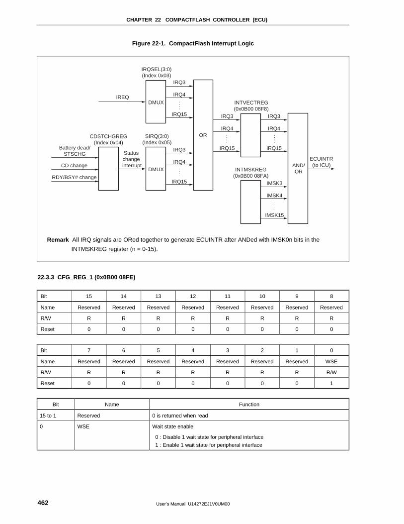
CHAPTER 22 COMPACTFLASH CONTROLLER (ECU)
User’s Manual U14272EJ1V0UM00462
Figure 22-1. CompactFlash Interrupt Logic
CDSTCHGREG(Index 0x04)
DMUX
DMUX
OR
AND/OR
SIRQ(3:0)(Index 0x05)
IRQSEL(3:0)(Index 0x03)
INTVECTREG(0x0B00 08F8)
INTMSKREG(0x0B00 08FA)
Status change interrupt
Battery dead/STSCHG
IREQ
CD change
RDY/BSY# change
IRQ3
IRQ4
IRQ15
IRQ3
IRQ4
IRQ15
IRQ3
IRQ4
IRQ15
IRQ3
IRQ4
IRQ15
IMSK3
IMSK4
IMSK15
ECUINTR(to ICU)
::
::
::
::
::
Remark All IRQ signals are ORed together to generate ECUINTR after ANDed with IMSK0n bits in the
INTMSKREG register (n = 0-15).
22.3.3 CFG_REG_1 (0x0B00 08FE)
Bit 15 14 13 12 11 10 9 8
Name Reserved Reserved Reserved Reserved Reserved Reserved Reserved Reserved
R/W R R R R R R R R
Reset 0 0 0 0 0 0 0 0
Bit 7 6 5 4 3 2 1 0
Name Reserved Reserved Reserved Reserved Reserved Reserved Reserved WSE
R/W R R R R R R R R/W
Reset 0 0 0 0 0 0 0 1
Bit Name Function
15 to 1 Reserved 0 is returned when read
0 WSE Wait state enable
0 : Disable 1 wait state for peripheral interface
1 : Enable 1 wait state for peripheral interface
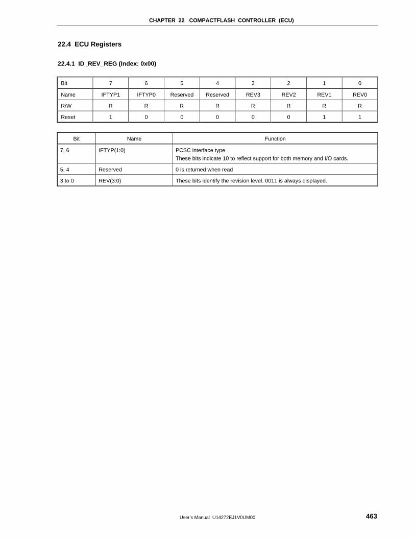
CHAPTER 22 COMPACTFLASH CONTROLLER (ECU)
User’s Manual U14272EJ1V0UM00 463
22.4 ECU Registers
22.4.1 ID_REV_REG (Index: 0x00)
Bit 7 6 5 4 3 2 1 0
Name IFTYP1 IFTYP0 Reserved Reserved REV3 REV2 REV1 REV0
R/W R R R R R R R R
Reset 1 0 0 0 0 0 1 1
Bit Name Function
7, 6 IFTYP(1:0) PCSC interface type
These bits indicate 10 to reflect support for both memory and I/O cards.
5, 4 Reserved 0 is returned when read
3 to 0 REV(3:0) These bits identify the revision level. 0011 is always displayed.
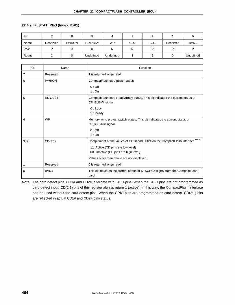
CHAPTER 22 COMPACTFLASH CONTROLLER (ECU)
User’s Manual U14272EJ1V0UM00464
22.4.2 IF_STAT_REG (Index: 0x01)
Bit 7 6 5 4 3 2 1 0
Name Reserved PWRON RDY/BSY WP CD2 CD1 Reserved BVD1
R/W R R R R R R R R
Reset 1 0 Undefined Undefined 1 1 0 Undefined
Bit Name Function
7 Reserved 1 is returned when read
6 PWRON CompactFlash card power status
0 : Off
1 : On
5 RDY/BSY CompactFlash card Ready/Busy status. This bit indicates the current status of
CF_BUSY# signal.
0 : Busy
1 : Ready
4 WP Memory write protect switch status. This bit indicates the current status of
CF_IOIS16# signal.
0 : Off
1 : On
3, 2 CD(2:1) Complement of the values of CD1# and CD2# on the CompactFlash interface Note
11: Active (CD pins are low level)
00 : Inactive (CD pins are high level)
Values other than above are not displayed.
1 Reserved 0 is returned when read
0 BVD1 This bit indicates the current status of STSCHG# signal from the CompactFlash
card.
Note The card detect pins, CD1# and CD2#, alternate with GPIO pins. When the GPIO pins are not programmed as
card detect input, CD(2:1) bits of this register always return 1 (active). In this way, the CompactFlash interface
can be used without the card detect pins. When the GPIO pins are programmed as card detect, CD(2:1) bits
are reflected in actual CD1# and CD2# pins status.
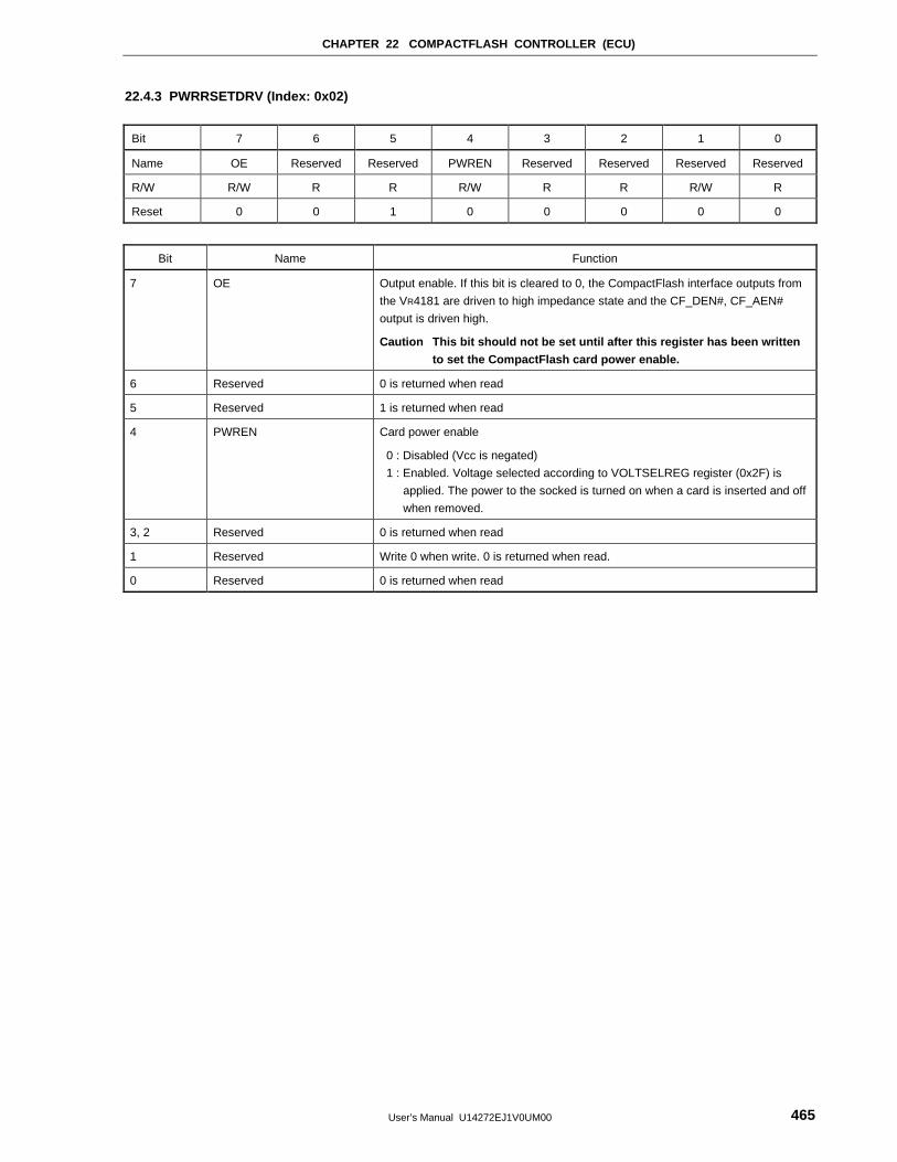
CHAPTER 22 COMPACTFLASH CONTROLLER (ECU)
User’s Manual U14272EJ1V0UM00 465
22.4.3 PWRRSETDRV (Index: 0x02)
Bit 7 6 5 4 3 2 1 0
Name OE Reserved Reserved PWREN Reserved Reserved Reserved Reserved
R/W R/W R R R/W R R R/W R
Reset 0 0 1 0 0 0 0 0
Bit Name Function
7 OE Output enable. If this bit is cleared to 0, the CompactFlash interface outputs from
the VR4181 are driven to high impedance state and the CF_DEN#, CF_AEN#
output is driven high.
Caution This bit should not be set until after this register has been written
to set the CompactFlash card power enable.
6 Reserved 0 is returned when read
5 Reserved 1 is returned when read
4 PWREN Card power enable
0 : Disabled (Vcc is negated)
1 : Enabled. Voltage selected according to VOLTSELREG register (0x2F) is
applied. The power to the socked is turned on when a card is inserted and off
when removed.
3, 2 Reserved 0 is returned when read
1 Reserved Write 0 when write. 0 is returned when read.
0 Reserved 0 is returned when read
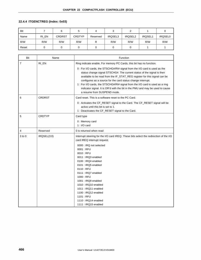
CHAPTER 22 COMPACTFLASH CONTROLLER (ECU)
User’s Manual U14272EJ1V0UM00466
22.4.4 ITGENCTREG (Index: 0x03)
Bit 7 6 5 4 3 2 1 0
Name RI_EN CRDRST CRDTYP Reserved IRQSEL3 IRQSEL2 IRQSEL1 IRQSEL0
R/W R/W R/W R/W R R/W R/W R/W R/W
Reset 0 0 0 0 0 0 1 1
Bit Name Function
7 RI_EN Ring indicate enable. For memory PC Cards, this bit has no function.
0 : For I/O cards, the STSCHG#/RI# signal from the I/O card is used as the
status change signal STSCHG#. The current status of the signal is then
available to be read from the IF_STAT_REG register for this signal can be
configures as a source for the card status change interrupt.
1 : For I/O cards, the STSCHG#/RI# signal from the I/O card is used as a ring
indicator signal. It is OR’d with the bit in the PMU and may be used to cause
a resume from SUSPEND mode.
6 CRDRST Card reset. This is a software reset to the PC Card.
0 : Activates the CF_RESET signal to the Card. The CF_RESET signal will be
active until this bit is set to 1.
1 : Deactivates the CF_RESET signal to the Card.
5 CRDTYP Card type
0 : Memory card
1 : I/O card
4 Reserved 0 is returned when read
3 to 0 IRQSEL(3:0) Interrupt steering for the I/O card IREQ. These bits select the redirection of the I/O
card IREQ interrupt request.
0000 : IRQ not selected
0001 : RFU
0010 : RFU
0011 : IRQ3 enabled
0100 : IRQ4 enabled
0101 : IRQ5 enabled
0110 : RFU
0111 : IRQ7 enabled
1000 : RFU
1001 : IRQ9 enabled
1010 : IRQ10 enabled
1011 : IRQ11 enabled
1100 : IRQ12 enabled
1101 : RFU
1110 : IRQ14 enabled
1111 : IRQ15 enabled
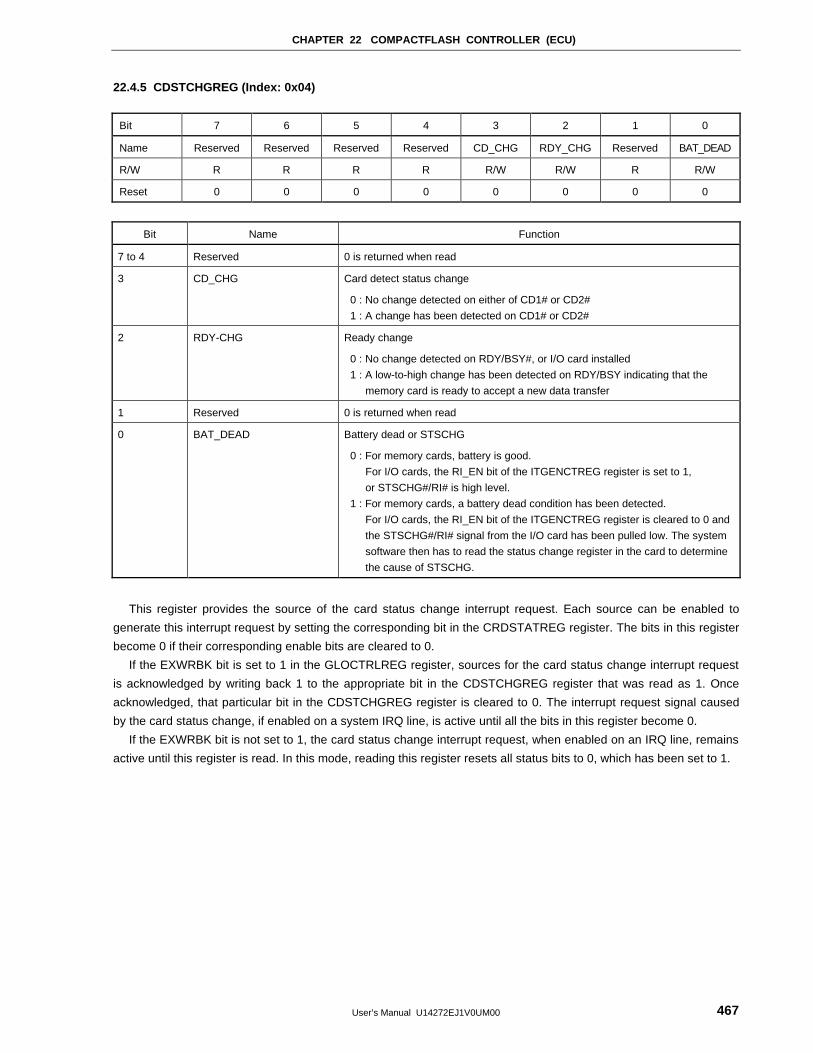
CHAPTER 22 COMPACTFLASH CONTROLLER (ECU)
User’s Manual U14272EJ1V0UM00 467
22.4.5 CDSTCHGREG (Index: 0x04)
Bit 7 6 5 4 3 2 1 0
Name Reserved Reserved Reserved Reserved CD_CHG RDY_CHG Reserved BAT_DEAD
R/W R R R R R/W R/W R R/W
Reset 0 0 0 0 0 0 0 0
Bit Name Function
7 to 4 Reserved 0 is returned when read
3 CD_CHG Card detect status change
0 : No change detected on either of CD1# or CD2#
1 : A change has been detected on CD1# or CD2#
2 RDY-CHG Ready change
0 : No change detected on RDY/BSY#, or I/O card installed
1 : A low-to-high change has been detected on RDY/BSY indicating that the
memory card is ready to accept a new data transfer
1 Reserved 0 is returned when read
0 BAT_DEAD Battery dead or STSCHG
0 : For memory cards, battery is good.
For I/O cards, the RI_EN bit of the ITGENCTREG register is set to 1,
or STSCHG#/RI# is high level.
1 : For memory cards, a battery dead condition has been detected.
For I/O cards, the RI_EN bit of the ITGENCTREG register is cleared to 0 and
the STSCHG#/RI# signal from the I/O card has been pulled low. The system
software then has to read the status change register in the card to determine
the cause of STSCHG.
This register provides the source of the card status change interrupt request. Each source can be enabled to
generate this interrupt request by setting the corresponding bit in the CRDSTATREG register. The bits in this register
become 0 if their corresponding enable bits are cleared to 0.
If the EXWRBK bit is set to 1 in the GLOCTRLREG register, sources for the card status change interrupt request
is acknowledged by writing back 1 to the appropriate bit in the CDSTCHGREG register that was read as 1. Once
acknowledged, that particular bit in the CDSTCHGREG register is cleared to 0. The interrupt request signal caused
by the card status change, if enabled on a system IRQ line, is active until all the bits in this register become 0.
If the EXWRBK bit is not set to 1, the card status change interrupt request, when enabled on an IRQ line, remains
active until this register is read. In this mode, reading this register resets all status bits to 0, which has been set to 1.
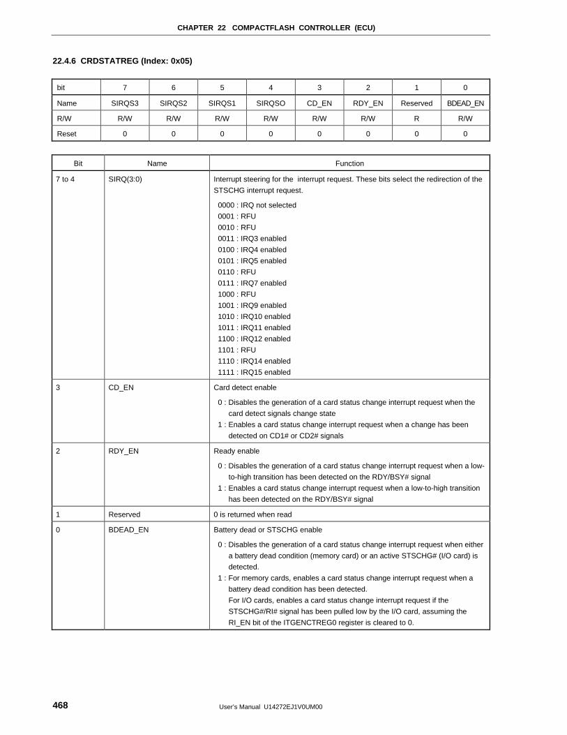
CHAPTER 22 COMPACTFLASH CONTROLLER (ECU)
User’s Manual U14272EJ1V0UM00468
22.4.6 CRDSTATREG (Index: 0x05)
bit 7 6 5 4 3 2 1 0
Name SIRQS3 SIRQS2 SIRQS1 SIRQSO CD_EN RDY_EN Reserved BDEAD_EN
R/W R/W R/W R/W R/W R/W R/W R R/W
Reset 0 0 0 0 0 0 0 0
Bit Name Function
7 to 4 SIRQ(3:0) Interrupt steering for the interrupt request. These bits select the redirection of the
STSCHG interrupt request.
0000 : IRQ not selected
0001 : RFU
0010 : RFU
0011 : IRQ3 enabled
0100 : IRQ4 enabled
0101 : IRQ5 enabled
0110 : RFU
0111 : IRQ7 enabled
1000 : RFU
1001 : IRQ9 enabled
1010 : IRQ10 enabled
1011 : IRQ11 enabled
1100 : IRQ12 enabled
1101 : RFU
1110 : IRQ14 enabled
1111 : IRQ15 enabled
3 CD_EN Card detect enable
0 : Disables the generation of a card status change interrupt request when the
card detect signals change state
1 : Enables a card status change interrupt request when a change has been
detected on CD1# or CD2# signals
2 RDY_EN Ready enable
0 : Disables the generation of a card status change interrupt request when a low-
to-high transition has been detected on the RDY/BSY# signal
1 : Enables a card status change interrupt request when a low-to-high transition
has been detected on the RDY/BSY# signal
1 Reserved 0 is returned when read
0 BDEAD_EN Battery dead or STSCHG enable
0 : Disables the generation of a card status change interrupt request when either
a battery dead condition (memory card) or an active STSCHG# (I/O card) is
detected.
1 : For memory cards, enables a card status change interrupt request when a
battery dead condition has been detected.
For I/O cards, enables a card status change interrupt request if the
STSCHG#/RI# signal has been pulled low by the I/O card, assuming the
RI_EN bit of the ITGENCTREG0 register is cleared to 0.
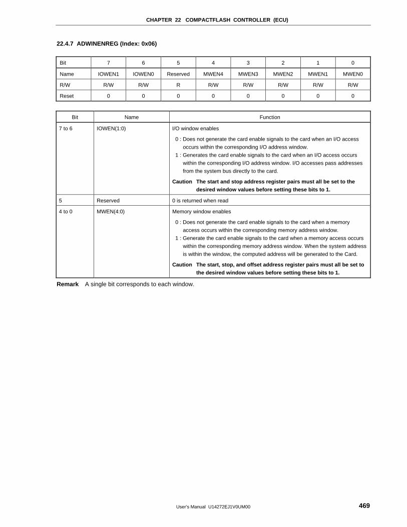
CHAPTER 22 COMPACTFLASH CONTROLLER (ECU)
User’s Manual U14272EJ1V0UM00 469
22.4.7 ADWINENREG (Index: 0x06)
Bit 7 6 5 4 3 2 1 0
Name IOWEN1 IOWEN0 Reserved MWEN4 MWEN3 MWEN2 MWEN1 MWEN0
R/W R/W R/W R R/W R/W R/W R/W R/W
Reset 0 0 0 0 0 0 0 0
Bit Name Function
7 to 6 IOWEN(1:0) I/O window enables
0 : Does not generate the card enable signals to the card when an I/O access
occurs within the corresponding I/O address window.
1 : Generates the card enable signals to the card when an I/O access occurs
within the corresponding I/O address window. I/O accesses pass addresses
from the system bus directly to the card.
Caution The start and stop address register pairs must all be set to the
desired window values before setting these bits to 1.
5 Reserved 0 is returned when read
4 to 0 MWEN(4:0) Memory window enables
0 : Does not generate the card enable signals to the card when a memory
access occurs within the corresponding memory address window.
1 : Generate the card enable signals to the card when a memory access occurs
within the corresponding memory address window. When the system address
is within the window, the computed address will be generated to the Card.
Caution The start, stop, and offset address register pairs must all be set to
the desired window values before setting these bits to 1.
Remark A single bit corresponds to each window.
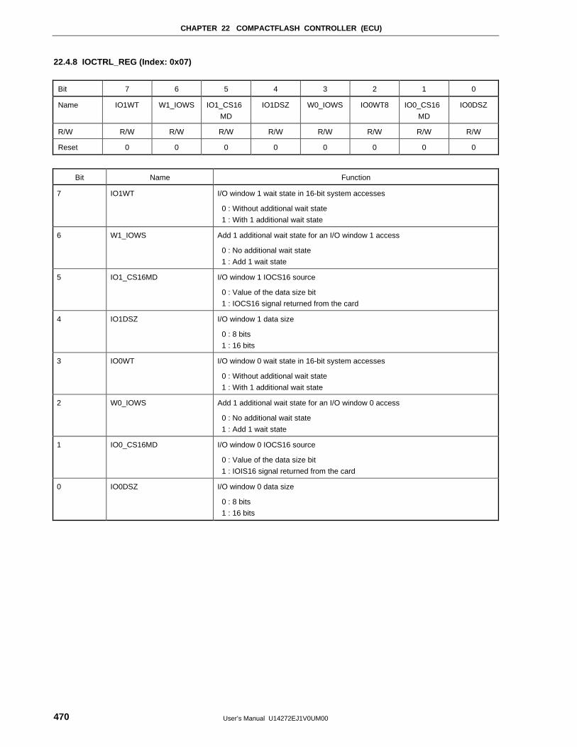
CHAPTER 22 COMPACTFLASH CONTROLLER (ECU)
User’s Manual U14272EJ1V0UM00470
22.4.8 IOCTRL_REG (Index: 0x07)
Bit 7 6 5 4 3 2 1 0
Name IO1WT W1_IOWS IO1_CS16
MD
IO1DSZ W0_IOWS IO0WT8 IO0_CS16
MD
IO0DSZ
R/W R/W R/W R/W R/W R/W R/W R/W R/W
Reset 0 0 0 0 0 0 0 0
Bit Name Function
7 IO1WT I/O window 1 wait state in 16-bit system accesses
0 : Without additional wait state
1 : With 1 additional wait state
6 W1_IOWS Add 1 additional wait state for an I/O window 1 access
0 : No additional wait state
1 : Add 1 wait state
5 IO1_CS16MD I/O window 1 IOCS16 source
0 : Value of the data size bit
1 : IOCS16 signal returned from the card
4 IO1DSZ I/O window 1 data size
0 : 8 bits
1 : 16 bits
3 IO0WT I/O window 0 wait state in 16-bit system accesses
0 : Without additional wait state
1 : With 1 additional wait state
2 W0_IOWS Add 1 additional wait state for an I/O window 0 access
0 : No additional wait state
1 : Add 1 wait state
1 IO0_CS16MD I/O window 0 IOCS16 source
0 : Value of the data size bit
1 : IOIS16 signal returned from the card
0 IO0DSZ I/O window 0 data size
0 : 8 bits
1 : 16 bits
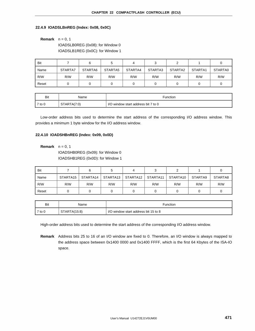
CHAPTER 22 COMPACTFLASH CONTROLLER (ECU)
User’s Manual U14272EJ1V0UM00 471
22.4.9 IOADSLBnREG (Index: 0x08, 0x0C)
Remark n = 0, 1
IOADSLB0REG (0x08): for Window 0
IOADSLB1REG (0x0C): for Window 1
Bit 7 6 5 4 3 2 1 0
Name STARTA7 STARTA6 STARTA5 STARTA4 STARTA3 STARTA2 STARTA1 STARTA0
R/W R/W R/W R/W R/W R/W R/W R/W R/W
Reset 0 0 0 0 0 0 0 0
Bit Name Function
7 to 0 STARTA(7:0) I/O window start address bit 7 to 0
Low-order address bits used to determine the start address of the corresponding I/O address window. This
provides a minimum 1 byte window for the I/O address window.
22.4.10 IOADSHBnREG (Index: 0x09, 0x0D)
Remark n = 0, 1
IOADSHB0REG (0x09): for Window 0
IOADSHB1REG (0x0D): for Window 1
Bit 7 6 5 4 3 2 1 0
Name STARTA15 STARTA14 STARTA13 STARTA12 STARTA11 STARTA10 STARTA9 STARTA8
R/W R/W R/W R/W R/W R/W R/W R/W R/W
Reset 0 0 0 0 0 0 0 0
Bit Name Function
7 to 0 STARTA(15:8) I/O window start address bit 15 to 8
High-order address bits used to determine the start address of the corresponding I/O address window.
Remark Address bits 25 to 16 of an I/O window are fixed to 0. Therefore, an I/O window is always mapped to
the address space between 0x1400 0000 and 0x1400 FFFF, which is the first 64 Kbytes of the ISA-IO
space.
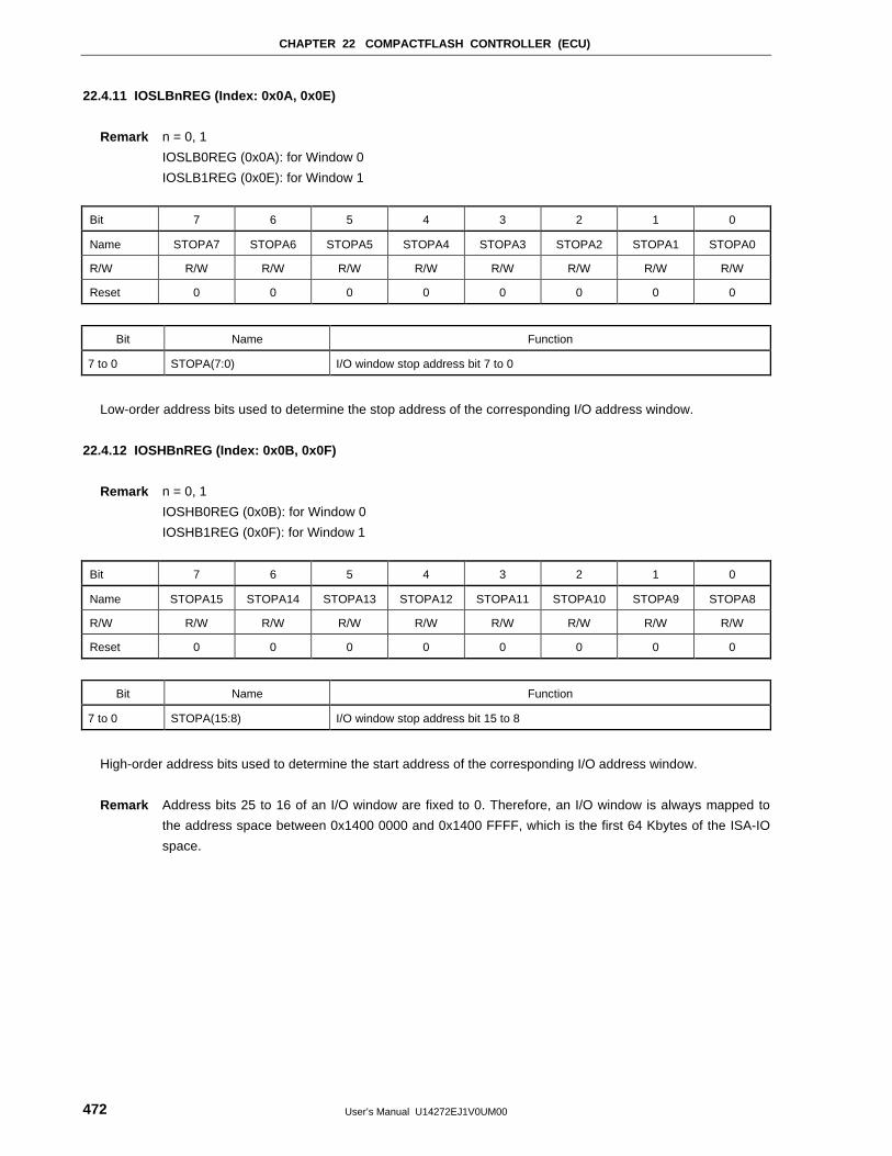
CHAPTER 22 COMPACTFLASH CONTROLLER (ECU)
User’s Manual U14272EJ1V0UM00472
22.4.11 IOSLBnREG (Index: 0x0A, 0x0E)
Remark n = 0, 1
IOSLB0REG (0x0A): for Window 0
IOSLB1REG (0x0E): for Window 1
Bit 7 6 5 4 3 2 1 0
Name STOPA7 STOPA6 STOPA5 STOPA4 STOPA3 STOPA2 STOPA1 STOPA0
R/W R/W R/W R/W R/W R/W R/W R/W R/W
Reset 0 0 0 0 0 0 0 0
Bit Name Function
7 to 0 STOPA(7:0) I/O window stop address bit 7 to 0
Low-order address bits used to determine the stop address of the corresponding I/O address window.
22.4.12 IOSHBnREG (Index: 0x0B, 0x0F)
Remark n = 0, 1
IOSHB0REG (0x0B): for Window 0
IOSHB1REG (0x0F): for Window 1
Bit 7 6 5 4 3 2 1 0
Name STOPA15 STOPA14 STOPA13 STOPA12 STOPA11 STOPA10 STOPA9 STOPA8
R/W R/W R/W R/W R/W R/W R/W R/W R/W
Reset 0 0 0 0 0 0 0 0
Bit Name Function
7 to 0 STOPA(15:8) I/O window stop address bit 15 to 8
High-order address bits used to determine the start address of the corresponding I/O address window.
Remark Address bits 25 to 16 of an I/O window are fixed to 0. Therefore, an I/O window is always mapped to
the address space between 0x1400 0000 and 0x1400 FFFF, which is the first 64 Kbytes of the ISA-IO
space.
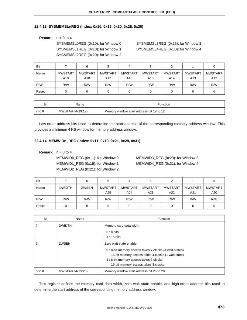
CHAPTER 22 COMPACTFLASH CONTROLLER (ECU)
User’s Manual U14272EJ1V0UM00 473
22.4.13 SYSMEMSLnREG (Index: 0x10, 0x18, 0x20, 0x28, 0x30)
Remark n = 0 to 4
SYSMEMSL0REG (0x10): for Window 0 SYSMEMSL3REG (0x28): for Window 3
SYSMEMSL1REG (0x18): for Window 1 SYSMEMSL4REG (0x30): for Window 4
SYSMEMSL2REG (0x20): for Window 2
Bit 7 6 5 4 3 2 1 0
Name MWSTART
A19
MWSTART
A18
MWSTART
A17
MWSTART
A16
MWSTART
A15
MWSTART
A14
MWSTART
A13
MWSTART
A12
R/W R/W R/W R/W R/W R/W R/W R/W R/W
Reset 0 0 0 0 0 0 0 0
Bit Name Function
7 to 0 MWSTARTA(19:12) Memory window start address bit 19 to 12
Low-order address bits used to determine the start address of the corresponding memory address window. This
provides a minimum 4 KB window for memory address window.
22.4.14 MEMWIDn_REG (Index: 0x11, 0x19, 0x21, 0x29, 0x31)
Remark n = 0 to 4
MEMWID0_REG (0x11): for Window 0 MEMWID3_REG (0x29): for Window 3
MEMWID1_REG (0x19): for Window 1 MEMWID4_REG (0x31): for Window 4
MEMWID2_REG (0x21): for Window 2
Bit 7 6 5 4 3 2 1 0
Name DWIDTH ZWSEN MWSTART
A25
MWSTART
A24
MWSTART
A23
MWSTART
A22
MWSTART
A21
MWSTART
A20
R/W R/W R/W R/W R\W R/W R/W R/W R/W
Reset 0 0 0 0 0 0 0 0
Bit Name Function
7 DWIDTH Memory card data width
0 : 8 bits
1 : 16 bits
6 ZWSEN Zero wait state enable
0 : 8-bit memory access takes 7 clocks (4 wait states)
16 bit memory access takes 4 clocks (1 wait state)
1 : 8-bit memory access takes 3 clocks
16 bit memory access takes 3 clocks
5 to 0 MWSTARTA(25:20) Memory window start address bit 25 to 20
This register defines the memory card data width, zero wait state enable, and high-order address bits used to
determine the start address of the corresponding memory address window.
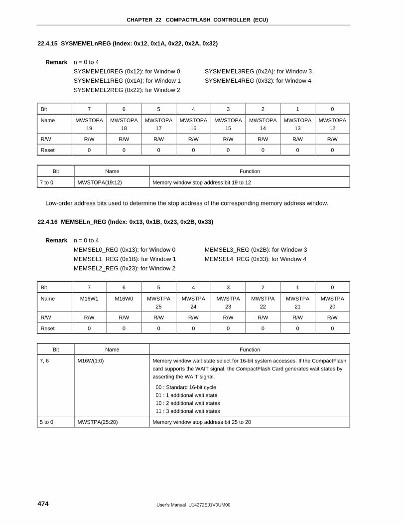
CHAPTER 22 COMPACTFLASH CONTROLLER (ECU)
User’s Manual U14272EJ1V0UM00474
22.4.15 SYSMEMELnREG (Index: 0x12, 0x1A, 0x22, 0x2A, 0x32)
Remark n = 0 to 4
SYSMEMEL0REG (0x12): for Window 0 SYSMEMEL3REG (0x2A): for Window 3
SYSMEMEL1REG (0x1A): for Window 1 SYSMEMEL4REG (0x32): for Window 4
SYSMEMEL2REG (0x22): for Window 2
Bit 7 6 5 4 3 2 1 0
Name MWSTOPA
19
MWSTOPA
18
MWSTOPA
17
MWSTOPA
16
MWSTOPA
15
MWSTOPA
14
MWSTOPA
13
MWSTOPA
12
R/W R/W R/W R/W R/W R/W R/W R/W R/W
Reset 0 0 0 0 0 0 0 0
Bit Name Function
7 to 0 MWSTOPA(19:12) Memory window stop address bit 19 to 12
Low-order address bits used to determine the stop address of the corresponding memory address window.
22.4.16 MEMSELn_REG (Index: 0x13, 0x1B, 0x23, 0x2B, 0x33)
Remark n = 0 to 4
MEMSEL0_REG (0x13): for Window 0 MEMSEL3_REG (0x2B): for Window 3
MEMSEL1_REG (0x1B): for Window 1 MEMSEL4_REG (0x33): for Window 4
MEMSEL2_REG (0x23): for Window 2
Bit 7 6 5 4 3 2 1 0
Name M16W1 M16W0 MWSTPA
25
MWSTPA
24
MWSTPA
23
MWSTPA
22
MWSTPA
21
MWSTPA
20
R/W R/W R/W R/W R/W R/W R/W R/W R/W
Reset 0 0 0 0 0 0 0 0
Bit Name Function
7, 6 M16W(1:0) Memory window wait state select for 16-bit system accesses. If the CompactFlash
card supports the WAIT signal, the CompactFlash Card generates wait states by
asserting the WAIT signal.
00 : Standard 16-bit cycle
01 : 1 additional wait state
10 : 2 additional wait states
11 : 3 additional wait states
5 to 0 MWSTPA(25:20) Memory window stop address bit 25 to 20
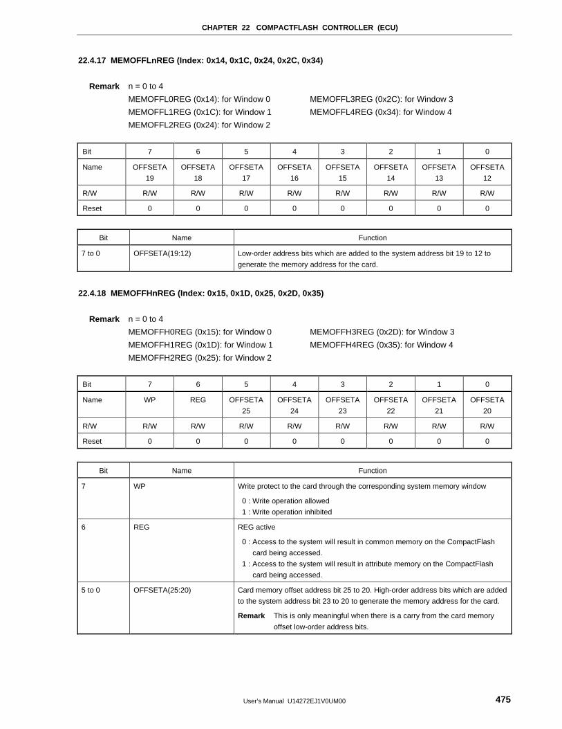
CHAPTER 22 COMPACTFLASH CONTROLLER (ECU)
User’s Manual U14272EJ1V0UM00 475
22.4.17 MEMOFFLnREG (Index: 0x14, 0x1C, 0x24, 0x2C, 0x34)
Remark n = 0 to 4
MEMOFFL0REG (0x14): for Window 0 MEMOFFL3REG (0x2C): for Window 3
MEMOFFL1REG (0x1C): for Window 1 MEMOFFL4REG (0x34): for Window 4
MEMOFFL2REG (0x24): for Window 2
Bit 7 6 5 4 3 2 1 0
Name OFFSETA
19
OFFSETA
18
OFFSETA
17
OFFSETA
16
OFFSETA
15
OFFSETA
14
OFFSETA
13
OFFSETA
12
R/W R/W R/W R/W R/W R/W R/W R/W R/W
Reset 0 0 0 0 0 0 0 0
Bit Name Function
7 to 0 OFFSETA(19:12) Low-order address bits which are added to the system address bit 19 to 12 to
generate the memory address for the card.
22.4.18 MEMOFFHnREG (Index: 0x15, 0x1D, 0x25, 0x2D, 0x35)
Remark n = 0 to 4
MEMOFFH0REG (0x15): for Window 0 MEMOFFH3REG (0x2D): for Window 3
MEMOFFH1REG (0x1D): for Window 1 MEMOFFH4REG (0x35): for Window 4
MEMOFFH2REG (0x25): for Window 2
Bit 7 6 5 4 3 2 1 0
Name WP REG OFFSETA
25
OFFSETA
24
OFFSETA
23
OFFSETA
22
OFFSETA
21
OFFSETA
20
R/W R/W R/W R/W R/W R/W R/W R/W R/W
Reset 0 0 0 0 0 0 0 0
Bit Name Function
7 WP Write protect to the card through the corresponding system memory window
0 : Write operation allowed
1 : Write operation inhibited
6 REG REG active
0 : Access to the system will result in common memory on the CompactFlash
card being accessed.
1 : Access to the system will result in attribute memory on the CompactFlash
card being accessed.
5 to 0 OFFSETA(25:20) Card memory offset address bit 25 to 20. High-order address bits which are added
to the system address bit 23 to 20 to generate the memory address for the card.
Remark This is only meaningful when there is a carry from the card memory
offset low-order address bits.
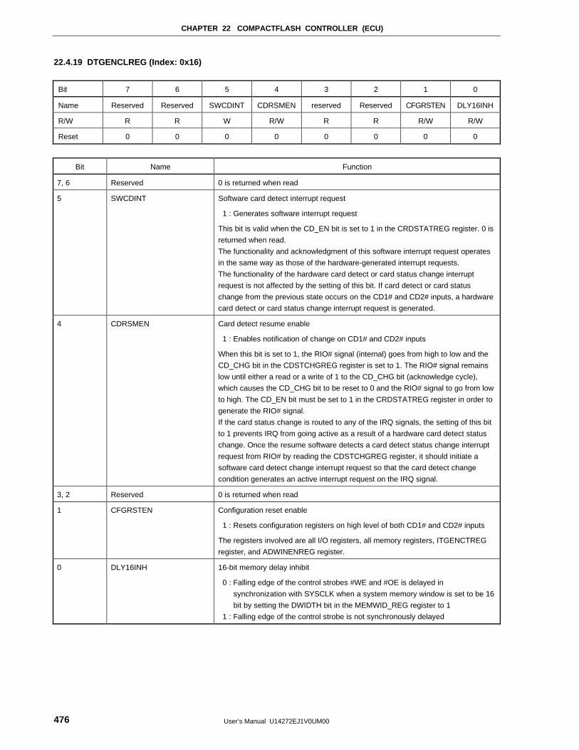
CHAPTER 22 COMPACTFLASH CONTROLLER (ECU)
User’s Manual U14272EJ1V0UM00476
22.4.19 DTGENCLREG (Index: 0x16)
Bit 7 6 5 4 3 2 1 0
Name Reserved Reserved SWCDINT CDRSMEN reserved Reserved CFGRSTEN DLY16INH
R/W R R W R/W R R R/W R/W
Reset 0 0 0 0 0 0 0 0
Bit Name Function
7, 6 Reserved 0 is returned when read
5 SWCDINT Software card detect interrupt request
1 : Generates software interrupt request
This bit is valid when the CD_EN bit is set to 1 in the CRDSTATREG register. 0 is
returned when read.
The functionality and acknowledgment of this software interrupt request operates
in the same way as those of the hardware-generated interrupt requests.
The functionality of the hardware card detect or card status change interrupt
request is not affected by the setting of this bit. If card detect or card status
change from the previous state occurs on the CD1# and CD2# inputs, a hardware
card detect or card status change interrupt request is generated.
4 CDRSMEN Card detect resume enable
1 : Enables notification of change on CD1# and CD2# inputs
When this bit is set to 1, the RIO# signal (internal) goes from high to low and the
CD_CHG bit in the CDSTCHGREG register is set to 1. The RIO# signal remains
low until either a read or a write of 1 to the CD_CHG bit (acknowledge cycle),
which causes the CD_CHG bit to be reset to 0 and the RIO# signal to go from low
to high. The CD_EN bit must be set to 1 in the CRDSTATREG register in order to
generate the RIO# signal.
If the card status change is routed to any of the IRQ signals, the setting of this bit
to 1 prevents IRQ from going active as a result of a hardware card detect status
change. Once the resume software detects a card detect status change interrupt
request from RIO# by reading the CDSTCHGREG register, it should initiate a
software card detect change interrupt request so that the card detect change
condition generates an active interrupt request on the IRQ signal.
3, 2 Reserved 0 is returned when read
1 CFGRSTEN Configuration reset enable
1 : Resets configuration registers on high level of both CD1# and CD2# inputs
The registers involved are all I/O registers, all memory registers, ITGENCTREG
register, and ADWINENREG register.
0 DLY16INH 16-bit memory delay inhibit
0 : Falling edge of the control strobes #WE and #OE is delayed in
synchronization with SYSCLK when a system memory window is set to be 16
bit by setting the DWIDTH bit in the MEMWID_REG register to 1
1 : Falling edge of the control strobe is not synchronously delayed
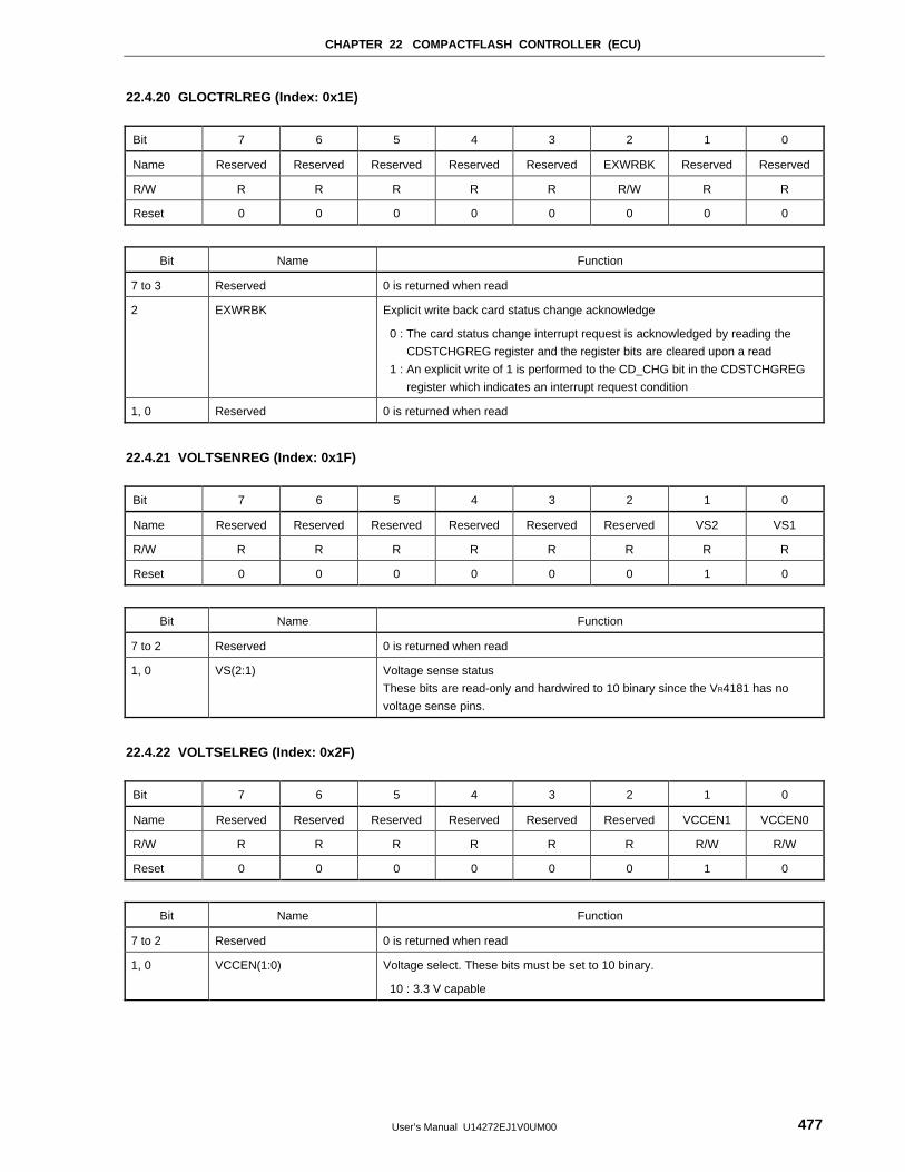
CHAPTER 22 COMPACTFLASH CONTROLLER (ECU)
User’s Manual U14272EJ1V0UM00 477
22.4.20 GLOCTRLREG (Index: 0x1E)
Bit 7 6 5 4 3 2 1 0
Name Reserved Reserved Reserved Reserved Reserved EXWRBK Reserved Reserved
R/W R R R R R R/W R R
Reset 0 0 0 0 0 0 0 0
Bit Name Function
7 to 3 Reserved 0 is returned when read
2 EXWRBK Explicit write back card status change acknowledge
0 : The card status change interrupt request is acknowledged by reading the
CDSTCHGREG register and the register bits are cleared upon a read
1 : An explicit write of 1 is performed to the CD_CHG bit in the CDSTCHGREG
register which indicates an interrupt request condition
1, 0 Reserved 0 is returned when read
22.4.21 VOLTSENREG (Index: 0x1F)
Bit 7 6 5 4 3 2 1 0
Name Reserved Reserved Reserved Reserved Reserved Reserved VS2 VS1
R/W R R R R R R R R
Reset 0 0 0 0 0 0 1 0
Bit Name Function
7 to 2 Reserved 0 is returned when read
1, 0 VS(2:1) Voltage sense status
These bits are read-only and hardwired to 10 binary since the VR4181 has no
voltage sense pins.
22.4.22 VOLTSELREG (Index: 0x2F)
Bit 7 6 5 4 3 2 1 0
Name Reserved Reserved Reserved Reserved Reserved Reserved VCCEN1 VCCEN0
R/W R R R R R R R/W R/W
Reset 0 0 0 0 0 0 1 0
Bit Name Function
7 to 2 Reserved 0 is returned when read
1, 0 VCCEN(1:0) Voltage select. These bits must be set to 10 binary.
10 : 3.3 V capable

User’s Manual U14272EJ1V0UM00478
[MEMO]
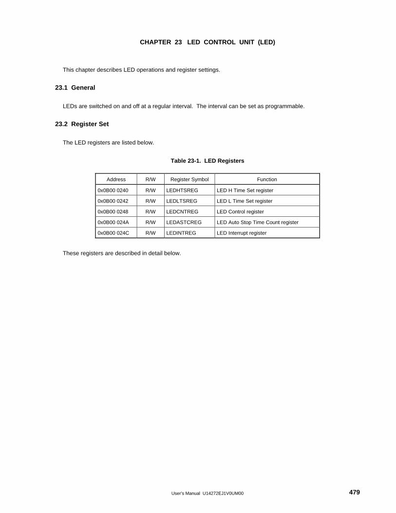
User’s Manual U14272EJ1V0UM00 479
CHAPTER 23 LED CONTROL UNIT (LED)
This chapter describes LED operations and register settings.
23.1 General
LEDs are switched on and off at a regular interval. The interval can be set as programmable.
23.2 Register Set
The LED registers are listed below.
Table 23-1. LED Registers
Address R/W Register Symbol Function
0x0B00 0240 R/W LEDHTSREG LED H Time Set register
0x0B00 0242 R/W LEDLTSREG LED L Time Set register
0x0B00 0248 R/W LEDCNTREG LED Control register
0x0B00 024A R/W LEDASTCREG LED Auto Stop Time Count register
0x0B00 024C R/W LEDINTREG LED Interrupt register
These registers are described in detail below.
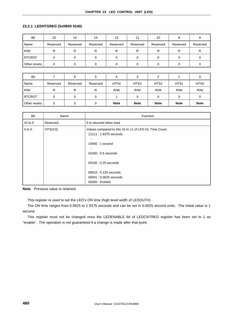
CHAPTER 23 LED CONTROL UNIT (LED)
User’s Manual U14272EJ1V0UM00480
23.2.1 LEDHTSREG (0x0B00 0240)
Bit 15 14 13 12 11 10 9 8
Name Reserved Reserved Reserved Reserved Reserved Reserved Reserved Reserved
R/W R R R R R R R R
RTCRST 0 0 0 0 0 0 0 0
Other resets 0 0 0 0 0 0 0 0
Bit 7 6 5 4 3 2 1 0
Name Reserved Reserved Reserved HTS4 HTS3 HTS2 HTS1 HTS0
R/W R R R R/W R/W R/W R/W R/W
RTCRST 0 0 0 1 0 0 0 0
Other resets 0 0 0 Note Note Note Note Note
Bit Name Function
15 to 5 Reserved 0 is returned when read
4 to 0 HTS(4:0) Values compared to bits 15 to 11 of LED HL Time Count.
11111 : 1.9375 seconds
:
10000 : 1 second
:
01000 : 0.5 seconds
:
00100 : 0.25 seconds
:
00010 : 0.125 seconds
00001 : 0.0625 seconds
00000 : Prohibit
Note Previous value is retained.
This register is used to set the LED’s ON time (high level width of LEDOUT#).
The ON time ranges from 0.0625 to 1.9375 seconds and can be set in 0.0625 second units. The initial value is 1
second.
This register must not be changed once the LEDENABLE bit of LEDCNTREG register has been set to 1 as
“enable”. The operation is not guaranteed if a change is made after that point.
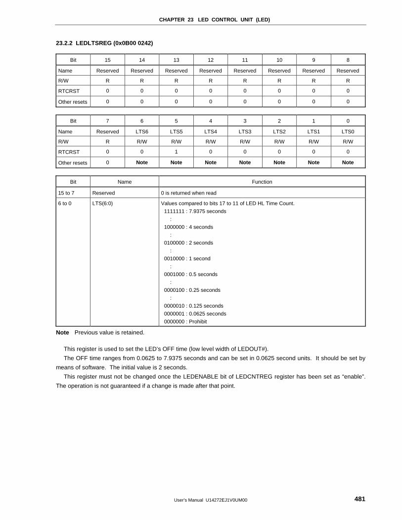
CHAPTER 23 LED CONTROL UNIT (LED)
User’s Manual U14272EJ1V0UM00 481
23.2.2 LEDLTSREG (0x0B00 0242)
Bit 15 14 13 12 11 10 9 8
Name Reserved Reserved Reserved Reserved Reserved Reserved Reserved Reserved
R/W R R R R R R R R
RTCRST 0 0 0 0 0 0 0 0
Other resets 0 0 0 0 0 0 0 0
Bit 7 6 5 4 3 2 1 0
Name Reserved LTS6 LTS5 LTS4 LTS3 LTS2 LTS1 LTS0
R/W R R/W R/W R/W R/W R/W R/W R/W
RTCRST 0 0 1 0 0 0 0 0
Other resets 0 Note Note Note Note Note Note Note
Bit Name Function
15 to 7 Reserved 0 is returned when read
6 to 0 LTS(6:0) Values compared to bits 17 to 11 of LED HL Time Count.
1111111 : 7.9375 seconds
:
1000000 : 4 seconds
:
0100000 : 2 seconds
:
0010000 : 1 second
:
0001000 : 0.5 seconds
:
0000100 : 0.25 seconds
:
0000010 : 0.125 seconds
0000001 : 0.0625 seconds
0000000 : Prohibit
Note Previous value is retained.
This register is used to set the LED’s OFF time (low level width of LEDOUT#).
The OFF time ranges from 0.0625 to 7.9375 seconds and can be set in 0.0625 second units. It should be set by
means of software. The initial value is 2 seconds.
This register must not be changed once the LEDENABLE bit of LEDCNTREG register has been set as “enable”.
The operation is not guaranteed if a change is made after that point.
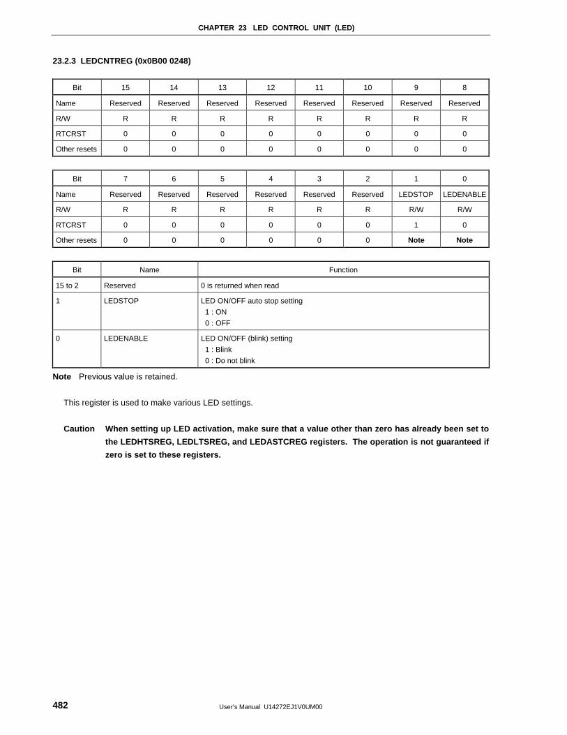
CHAPTER 23 LED CONTROL UNIT (LED)
User’s Manual U14272EJ1V0UM00482
23.2.3 LEDCNTREG (0x0B00 0248)
Bit 15 14 13 12 11 10 9 8
Name Reserved Reserved Reserved Reserved Reserved Reserved Reserved Reserved
R/W R R R R R R R R
RTCRST 0 0 0 0 0 0 0 0
Other resets 0 0 0 0 0 0 0 0
Bit 7 6 5 4 3 2 1 0
Name Reserved Reserved Reserved Reserved Reserved Reserved LEDSTOP LEDENABLE
R/W R R R R R R R/W R/W
RTCRST 0 0 0 0 0 0 1 0
Other resets 0 0 0 0 0 0 Note Note
Bit Name Function
15 to 2 Reserved 0 is returned when read
1 LEDSTOP LED ON/OFF auto stop setting
1 : ON
0 : OFF
0 LEDENABLE LED ON/OFF (blink) setting
1 : Blink
0 : Do not blink
Note Previous value is retained.
This register is used to make various LED settings.
Caution When setting up LED activation, make sure that a value other than zero has already been set to
the LEDHTSREG, LEDLTSREG, and LEDASTCREG registers. The operation is not guaranteed if
zero is set to these registers.
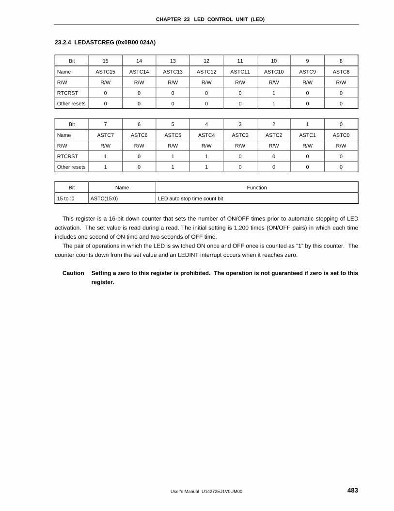
CHAPTER 23 LED CONTROL UNIT (LED)
User’s Manual U14272EJ1V0UM00 483
23.2.4 LEDASTCREG (0x0B00 024A)
Bit 15 14 13 12 11 10 9 8
Name ASTC15 ASTC14 ASTC13 ASTC12 ASTC11 ASTC10 ASTC9 ASTC8
R/W R/W R/W R/W R/W R/W R/W R/W R/W
RTCRST 0 0 0 0 0 1 0 0
Other resets 0 0 0 0 0 1 0 0
Bit 7 6 5 4 3 2 1 0
Name ASTC7 ASTC6 ASTC5 ASTC4 ASTC3 ASTC2 ASTC1 ASTC0
R/W R/W R/W R/W R/W R/W R/W R/W R/W
RTCRST 1 0 1 1 0 0 0 0
Other resets 1 0 1 1 0 0 0 0
Bit Name Function
15 to :0 ASTC(15:0) LED auto stop time count bit
This register is a 16-bit down counter that sets the number of ON/OFF times prior to automatic stopping of LED
activation. The set value is read during a read. The initial setting is 1,200 times (ON/OFF pairs) in which each time
includes one second of ON time and two seconds of OFF time.
The pair of operations in which the LED is switched ON once and OFF once is counted as “1” by this counter. The
counter counts down from the set value and an LEDINT interrupt occurs when it reaches zero.
Caution Setting a zero to this register is prohibited. The operation is not guaranteed if zero is set to this
register.
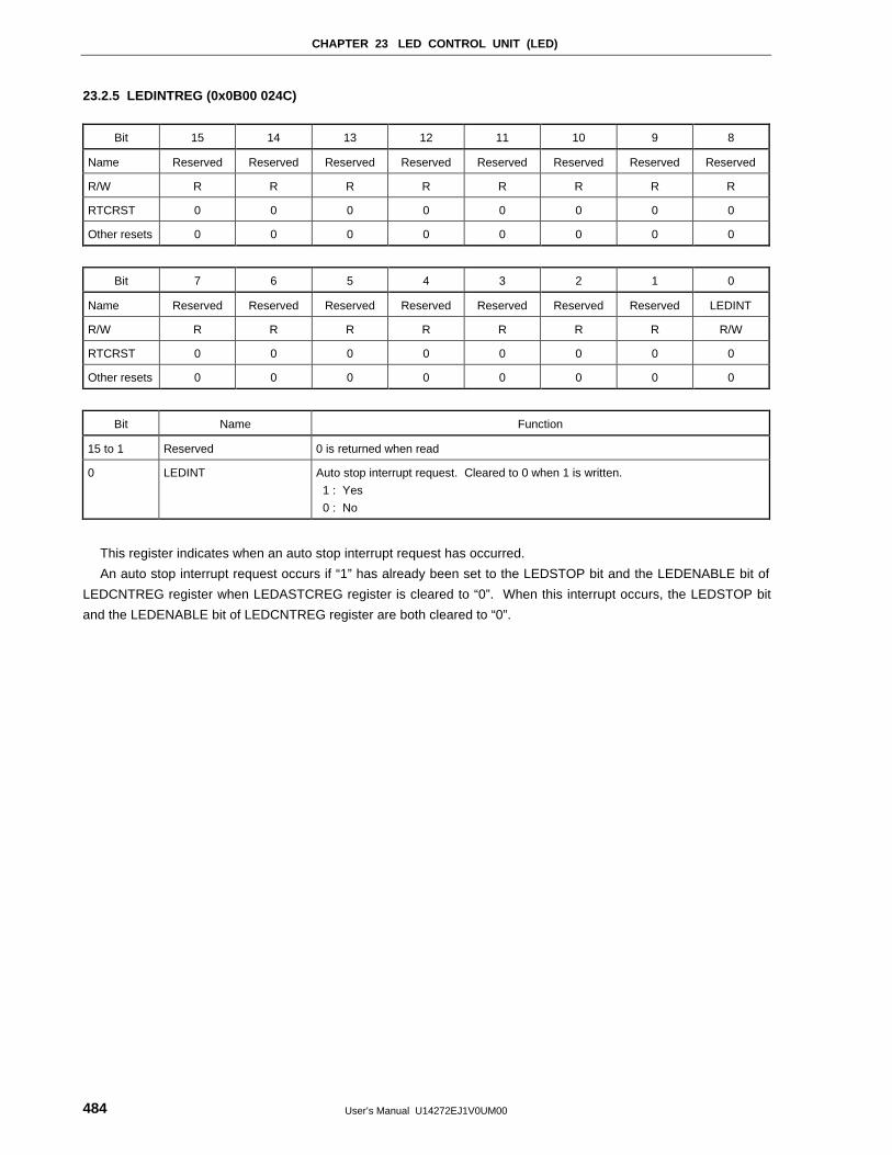
CHAPTER 23 LED CONTROL UNIT (LED)
User’s Manual U14272EJ1V0UM00484
23.2.5 LEDINTREG (0x0B00 024C)
Bit 15 14 13 12 11 10 9 8
Name Reserved Reserved Reserved Reserved Reserved Reserved Reserved Reserved
R/W R R R R R R R R
RTCRST 0 0 0 0 0 0 0 0
Other resets 0 0 0 0 0 0 0 0
Bit 7 6 5 4 3 2 1 0
Name Reserved Reserved Reserved Reserved Reserved Reserved Reserved LEDINT
R/W R R R R R R R R/W
RTCRST 0 0 0 0 0 0 0 0
Other resets 0 0 0 0 0 0 0 0
Bit Name Function
15 to 1 Reserved 0 is returned when read
0 LEDINT Auto stop interrupt request. Cleared to 0 when 1 is written.
1 : Yes
0 : No
This register indicates when an auto stop interrupt request has occurred.
An auto stop interrupt request occurs if “1” has already been set to the LEDSTOP bit and the LEDENABLE bit of
LEDCNTREG register when LEDASTCREG register is cleared to “0”. When this interrupt occurs, the LEDSTOP bit
and the LEDENABLE bit of LEDCNTREG register are both cleared to “0”.
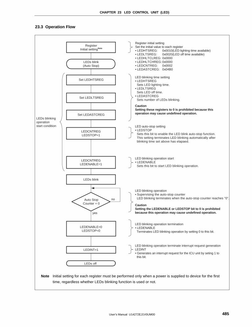
CHAPTER 23 LED CONTROL UNIT (LED)
User’s Manual U14272EJ1V0UM00 485
23.3 Operation Flow
Set LEDHTSREG
Set LEDLTSREG
LEDCNTREGLEDSTOP=1
Set LEDASTCREG
LEDCNTREGLEDENABLE=1
LED blinking time setting• LEDHTSREG Sets LED lighting time.• LEDLTSREG Sets LED off time.• LEDASTCREG Sets number of LEDs blinking.
LED auto-stop setting• LEDSTOP Sets this bit to enable the LED blink auto-stop function. This setting terminates LED blinking automatically after blinking time set above has elapaed.
LED blinking operation start• LEDENABLE Sets this bit to start LED blinking operation.
CautionSetting these registers to 0 is prohibited because thisoperation may cause undefined operation.
LED blinking operation• Supervising the auto-stop counter LED blinking terminates when the auto-stop counter reaches "0".
LED blinking operation termination• LEDENABLE Terminates LED blinking operation by setting 0 to this bit.
LED blinking operation terminate interrupt request generationLEDINT• Generates an interrupt request for the ICU unit by seting 1 to this bit.
CautionSetting the LEDENABLE or LEDSTOP bit to 0 is prohibitedbecause this operation may cause undefined operation.yes
no
LEDENABLE=0LEDSTOP=0
LEDINT=1
Register initial settingSet the initial value to each register• LEDHTSREG:• LEDLTSREG:• LEDHLTCLREG:• LEDHLTCHREG:• LEDCNTREG:• LEDASTCREG:
0x0010(LED lighting time available)0x0020(LED off time available)0x00000x00000x00020x04B0
LEDs blinkingoperationstart condition
LEDs blink
RegisterInitial settingNote
LEDs blink(Auto Stop)
Auto StopCounter = 0
LEDs off
Note Initial setting for each register must be performed only when a power is supplied to device for the first
time, regardless whether LEDs blinking function is used or not.

User’s Manual U14272EJ1V0UM00486
[MEMO]
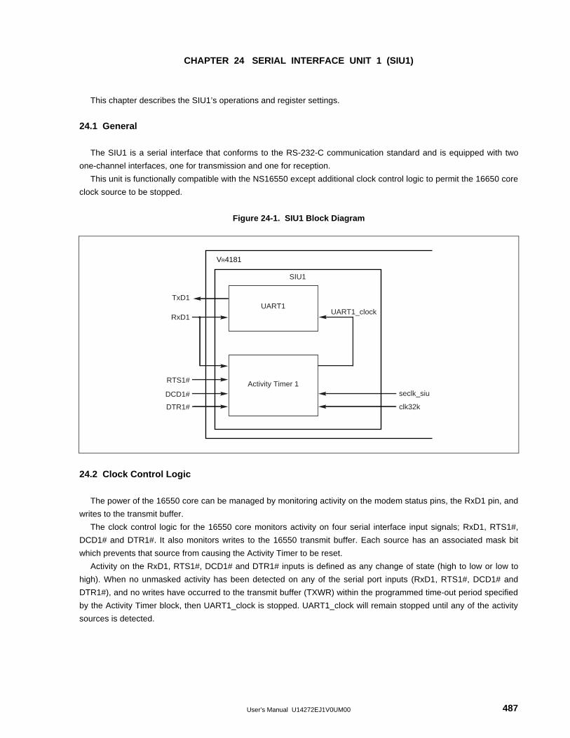
User’s Manual U14272EJ1V0UM00 487
CHAPTER 24 SERIAL INTERFACE UNIT 1 (SIU1)
This chapter describes the SIU1’s operations and register settings.
24.1 General
The SIU1 is a serial interface that conforms to the RS-232-C communication standard and is equipped with two
one-channel interfaces, one for transmission and one for reception.
This unit is functionally compatible with the NS16550 except additional clock control logic to permit the 16650 core
clock source to be stopped.
Figure 24-1. SIU1 Block Diagram
VR4181
UART1
RxD1
TxD1
RTS1# Activity Timer 1
DTR1#
DCD1#
clk32k
seclk_siu
UART1_clock
SIU1
24.2 Clock Control Logic
The power of the 16550 core can be managed by monitoring activity on the modem status pins, the RxD1 pin, and
writes to the transmit buffer.
The clock control logic for the 16550 core monitors activity on four serial interface input signals; RxD1, RTS1#,
DCD1# and DTR1#. It also monitors writes to the 16550 transmit buffer. Each source has an associated mask bit
which prevents that source from causing the Activity Timer to be reset.
Activity on the RxD1, RTS1#, DCD1# and DTR1# inputs is defined as any change of state (high to low or low to
high). When no unmasked activity has been detected on any of the serial port inputs (RxD1, RTS1#, DCD1# and
DTR1#), and no writes have occurred to the transmit buffer (TXWR) within the programmed time-out period specified
by the Activity Timer block, then UART1_clock is stopped. UART1_clock will remain stopped until any of the activity
sources is detected.
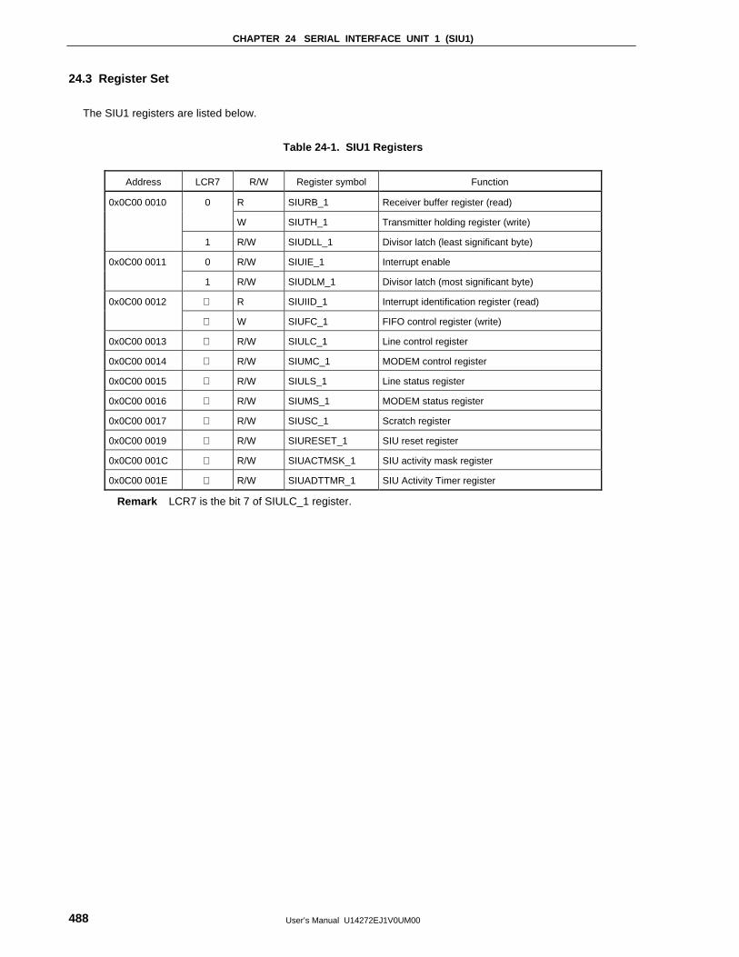
CHAPTER 24 SERIAL INTERFACE UNIT 1 (SIU1)
User’s Manual U14272EJ1V0UM00488
24.3 Register Set
The SIU1 registers are listed below.
Table 24-1. SIU1 Registers
Address LCR7 R/W Register symbol Function
0x0C00 0010 0 R SIURB_1 Receiver buffer register (read)
W SIUTH_1 Transmitter holding register (write)
1 R/W SIUDLL_1 Divisor latch (least significant byte)
0x0C00 0011 0 R/W SIUIE_1 Interrupt enable
1 R/W SIUDLM_1 Divisor latch (most significant byte)
0x0C00 0012 R SIUIID_1 Interrupt identification register (read)
W SIUFC_1 FIFO control register (write)
0x0C00 0013 R/W SIULC_1 Line control register
0x0C00 0014 R/W SIUMC_1 MODEM control register
0x0C00 0015 R/W SIULS_1 Line status register
0x0C00 0016 R/W SIUMS_1 MODEM status register
0x0C00 0017 R/W SIUSC_1 Scratch register
0x0C00 0019 R/W SIURESET_1 SIU reset register
0x0C00 001C R/W SIUACTMSK_1 SIU activity mask register
0x0C00 001E R/W SIUADTTMR_1 SIU Activity Timer register
Remark LCR7 is the bit 7 of SIULC_1 register.

CHAPTER 24 SERIAL INTERFACE UNIT 1 (SIU1)
User’s Manual U14272EJ1V0UM00 489
24.3.1 SIURB_1 (0x0C00 0010: LCR7 = 0, Read)
Bit 7 6 5 4 3 2 1 0
Name RXD7 RXD6 RXD5 RXD4 RXD3 RXD2 RXD1 RXD0
R/W R R R R R R R R
RTCRST 0 0 0 0 0 0 0 0
Other resets 0 0 0 0 0 0 0 0
Bit Name Function
7 to 0 RXD(7:0) Serial receive data
This register stores receive data used in serial communications.
To access this register, set LCR7 (bit 7 of SIULC_1 register) to 0.
24.3.2 SIUTH_1 (0x0C00 0010: LCR7 = 0, Write)
Bit 7 6 5 4 3 2 1 0
Name TXD7 TXD6 TXD5 TXD4 TXD3 TXD2 TXD1 TXD0
R/W W W W W W W W W
RTCRST 0 0 0 0 0 0 0 0
Other resets 0 0 0 0 0 0 0 0
Bit Name Function
7 to 0 TXD(7:0) Serial transmit data
This register stores transmit data used in serial communications.
To access this register, set LCR7 (bit 7 of SIULC_1 register) to 0.
24.3.3 SIUDLL_1 (0x0C00 0010: LCR7 = 1)
Bit 7 6 5 4 3 2 1 0
Name DLL7 DLL6 DLL5 DLL4 DLL3 DLL2 DLL1 DLL0
R/W R/W R/W R/W R/W R/W R/W R/W R/W
RTCRST 0 0 0 0 0 0 0 0
Other resets 0 0 0 0 0 0 0 0
Bit Name Function
7 to 0 DLL(7:0) Baud rate generator divisor (low-order byte)
This register is used to set the divisor (division rate) for the baud rate generator.
The data in this register and the upper 8-bit data in SIUDLM_1 register are together handled as 16-bit data.
To access this register, set LCR7 (bit 7 of SIULC_1 register) to 1.

CHAPTER 24 SERIAL INTERFACE UNIT 1 (SIU1)
User’s Manual U14272EJ1V0UM00490
24.3.4 SIUIE_1 (0x0C00 0011: LCR7 = 0)
Bit 7 6 5 4 3 2 1 0
Name Reserved Reserved Reserved Reserved IE3 IE2 IE1 IE0
R/W R R R R R/W R/W R/W R/W
RTCRST 0 0 0 0 0 0 0 0
Other resets 0 0 0 0 0 0 0 0
Bit Name Function
7 to 4 Reserved 0 is returned when read
3 IE3 MODEM status interrupt
1 : Interrupt enable
0 : Interrupt prohibit
2 IE2 Receive status interrupt
1 : Interrupt enable
0 : Interrupt prohibit
1 IE1 Transmitter holding register empty interrupt
1 : Interrupt enable
0 : Interrupt prohibit
0 IE0 Receive data interrupt or timeout interrupt in FIFO mode
1 : Interrupt enable
0 : Interrupt prohibit
This register is used to specify interrupt enable/prohibit settings for the five types of interrupt requests used by
SIU1.
These bits can be used to make the corresponding interrupt request output (INTR) active.
Overall use of interrupt functions can be halted by setting bits 0 to 3 of this register to 0.
When interrupts are prohibited, “pending” is not displayed in the IIR0 bit in the SIUIID_1 register even when the
interrupt condition has been met and INTR output does not become active.
Other functions in the system are not affected even though interrupts are prohibited and the settings in the line
status register (SIULS_1) and MODEM status register (SIUMS_1) are valid.
To access this register, set LCR7 (bit 7 of SIULC_1 register) to 0.

CHAPTER 24 SERIAL INTERFACE UNIT 1 (SIU1)
User’s Manual U14272EJ1V0UM00 491
24.3.5 SIUDLM_1 (0x0C00 0011: LCR7 = 1)
Bit 7 6 5 4 3 2 1 0
Name DLM7 DLM6 DLM5 DLM4 DLM3 DLM2 DLM1 DLM0
R/W R/W R/W R/W R/W R/W R/W R/W R/W
RTCRST 0 0 0 0 0 0 0 0
Other resets 0 0 0 0 0 0 0 0
Bit Name Function
7 to 0 DLM(7:0) Baud rate generator divisor (high-order byte)
This register is used to set the divisor (division rate) for the baud rate generator.
The data in this register and the lower 8-bit data in SIUDLL_1 register are together handled as 16-bit data.
To access this register, set LCR7 (bit 7 of SIULC_1 register) to 1.

CHAPTER 24 SERIAL INTERFACE UNIT 1 (SIU1)
User’s Manual U14272EJ1V0UM00492
Table 24-2. Correspondence between Baud Rates and Divisors
Baud rate Divisor 1-clock width
50 23040 20000
75 15360 13333
110 10473 9091
134.5 8565 7435
150 7680 6667
300 3840 3333
600 1920 1667
1200 920 833
1800 640 556
2000 573 500
2400 480 417
3600 320 278
4800 240 208
7200 160 139
9600 120 104
19200 60 52.1
38400 30 26.0
56000 21 17.9
128000 9 7.81
144000 8 6.94
192000 6 5.21
230400 5 4.34
288000 4 3.47
384000 3 2.60
576000 2 1.74
1152000 1 0.868
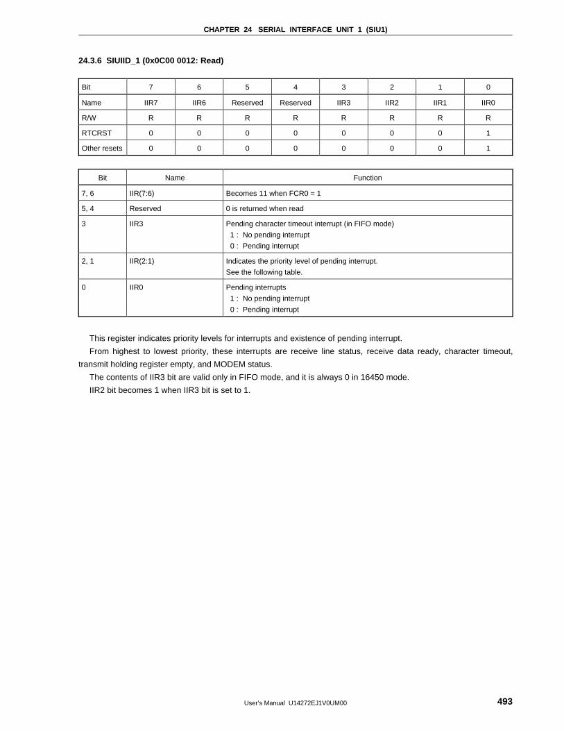
CHAPTER 24 SERIAL INTERFACE UNIT 1 (SIU1)
User’s Manual U14272EJ1V0UM00 493
24.3.6 SIUIID_1 (0x0C00 0012: Read)
Bit 7 6 5 4 3 2 1 0
Name IIR7 IIR6 Reserved Reserved IIR3 IIR2 IIR1 IIR0
R/W R R R R R R R R
RTCRST 0 0 0 0 0 0 0 1
Other resets 0 0 0 0 0 0 0 1
Bit Name Function
7, 6 IIR(7:6) Becomes 11 when FCR0 = 1
5, 4 Reserved 0 is returned when read
3 IIR3 Pending character timeout interrupt (in FIFO mode)
1 : No pending interrupt
0 : Pending interrupt
2, 1 IIR(2:1) Indicates the priority level of pending interrupt.
See the following table.
0 IIR0 Pending interrupts
1 : No pending interrupt
0 : Pending interrupt
This register indicates priority levels for interrupts and existence of pending interrupt.
From highest to lowest priority, these interrupts are receive line status, receive data ready, character timeout,
transmit holding register empty, and MODEM status.
The contents of IIR3 bit are valid only in FIFO mode, and it is always 0 in 16450 mode.
IIR2 bit becomes 1 when IIR3 bit is set to 1.
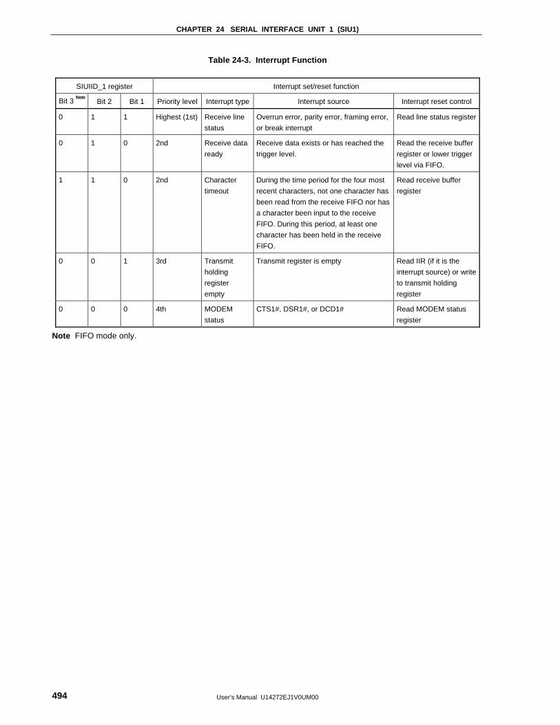
CHAPTER 24 SERIAL INTERFACE UNIT 1 (SIU1)
User’s Manual U14272EJ1V0UM00494
Table 24-3. Interrupt Function
SIUIID_1 register Interrupt set/reset function
Bit 3 Note
Bit 2 Bit 1 Priority level Interrupt type Interrupt source Interrupt reset control
0 1 1 Highest (1st) Receive line
status
Overrun error, parity error, framing error,
or break interrupt
Read line status register
0 1 0 2nd Receive data
ready
Receive data exists or has reached the
trigger level.
Read the receive buffer
register or lower trigger
level via FIFO.
1 1 0 2nd Character
timeout
During the time period for the four most
recent characters, not one character has
been read from the receive FIFO nor has
a character been input to the receive
FIFO. During this period, at least one
character has been held in the receive
FIFO.
Read receive buffer
register
0 0 1 3rd Transmit
holding
register
empty
Transmit register is empty Read IIR (if it is the
interrupt source) or write
to transmit holding
register
0 0 0 4th MODEM
status
CTS1#, DSR1#, or DCD1# Read MODEM status
register
Note FIFO mode only.

CHAPTER 24 SERIAL INTERFACE UNIT 1 (SIU1)
User’s Manual U14272EJ1V0UM00 495
24.3.7 SIUFC_1 (0x0C00 0012: Write)
Bit 7 6 5 4 3 2 1 0
Name FCR7 FCR6 Reserved Reserved FCR3 FCR2 FCR1 FCR0
R/W W W R R W W W W
RTCRST 0 0 0 0 0 0 0 0
Other resets 0 0 0 0 0 0 0 0
Bit Name Function
7, 6 FCR(7:6) Receive FIFO trigger level
11 : 14 bytes
10 : 8 bytes
01 : 4 bytes
00 : 0 bytes
5, 4 Reserved 0 is returned when read
3 FCR3 Switch between 16450 mode and FIFO mode
1 : From 16450 mode to FIFO mode
0 : From FIFO mode to 16450 mode
2 FCR2 Transmit FIFO clear/counter clear. Cleared to 0 when 1 is written.
1 : FIFO clear/counter clear
0 : Normal
1 FCR1 Receive FIFO clear/counter clear. Cleared to 0 when 1 is written.
1 : FIFO clear/counter clear
0 : Normal
0 FCR0 Receive/Transmit FIFO enable
1 : Enable
0 : Disable
This register is used to control the FIFOs: enable FIFO, clear FIFO, and set the receive FIFO trigger level.
CHAPTER 24 SERIAL INTERFACE UNIT 1 (SIU1)
User’s Manual U14272EJ1V0UM00496
• FIFO interrupt modes
When receive FIFO is enabled and receive interrupts are enabled, receive interrupts can occur as described
below.
1. When the FIFO is reached to the specified trigger level, a receive data ready interrupt occurs to inform the
CPU.
This interrupt is cleared when the FIFO goes below the trigger level.
2. When the FIFO is reached to the specified trigger level, the SIUIID_1 register indicates a receive data
ready interrupt.
As with the interrupt above, SUIID_1 register is cleared when the FIFO goes below the trigger level.
3. Receive line status interrupts are assigned a higher priority level than are receive data ready interrupts.
4. When characters are transferred from the shift register to the receive FIFO, 1 is set to the LSR0 bit.
The value of this bit returns to 0 when the FIFO becomes empty.
When receive FIFO is enabled and receive interrupts are enabled, receive FIFO timeout interrupts can occur as
described below.
1. The following are conditions under which FIFO timeout interrupts occur.
• At least one character is being stored in the FIFO.
• The time required for sending four characters has elapsed since the serial reception of the last
character (includes the time for two stop bits in cases where a stop bit has been specified).
• The time required for sending four characters has elapsed since the CPU last accessed the FIFO.
The time between receiving the last character and issuing a timeout interrupt is a maximum of 160 ms
when operating at 300 baud and receiving 12-bit data.
2. The transfer time for a character is calculated based on the baud rate clock for reception (internal) input
as clock signals (which is why the elapsed time is in proportion to the baud rate).
3. Once a timeout interrupt has occurred, the timeout interrupt is cleared and the timer is reset as soon as
the CPU reads one character from the receive FIFO.
4. If no timeout interrupt has occurred, the timer is reset when a new character is received or when the CPU
reads the receive FIFO.
CHAPTER 24 SERIAL INTERFACE UNIT 1 (SIU1)
User’s Manual U14272EJ1V0UM00 497
When transmit FIFO is enabled and transmit interrupts are enabled, transmit interrupts can occur as described
below.
1. When the transmit FIFO becomes empty, a transmit holding register empty interrupt occurs.
This interrupt is cleared when a character is written to the transmit holding register (from one to 16
characters can be written to the transmit FIFO during servicing of this interrupt), or when interrupt ID
register (SIUIID_1) is read.
2. If there are not at least two bytes of character data in the transmit FIFO between one time when LSR5 = 1
(transmit FIFO is empty) and the next time when LSR5 = 1, empty transmit FIFO status is reported to the
IIR bits after a delay period calculated as “the time for one character − the time for the last stop bit(s)”.
When transmit interrupts are enabled, the first transmit interrupt that occurs after the FCR0 (FIFO enable
bit) is overwritten is indicated immediately.
The priority level of the character timeout interrupt and receive FIFO trigger level interrupt is the same as that of
the receive data ready interrupt.
The priority level of the transmit FIFO empty interrupt is the same as that of the transmit holding register empty
interrupt.
Whether data to be transmitted exists or not in the transmit FIFO and the transmit shift register, check the
transmit block empty bit (bit 6) of the SIULS_1 register. It cannot be checked by the transmit holding register
empty bit (bit 5) of the SIULS_1 register, because this bit is used to check whether data to be transferred exists
or not in the transmit FIFO. Therefore, this bit cannot check if there is data in the transmit shift register.
• FIFO polling mode
When FCR0 = 1 (FIFO is enabled), if the value of any or all of the interrupt enable register (SIUIE_1) bits 3 to 0
becomes 0, SIU1 enters FIFO polling mode. Because the transmit block and receive blocks are controlled
separately, polling mode can be set for either or both blocks.
When in this mode, the status of the transmit block and/or receive block can be checked by reading the line
status register (SIULS_1) via a user program.
When in the FIFO polling mode, there is no notification when the trigger level is reached or when a timeout
occurs, but the receive FIFO and transmit FIFO can still store characters as they normally do.
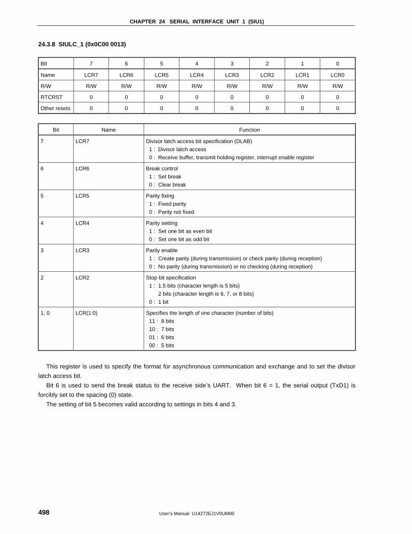
CHAPTER 24 SERIAL INTERFACE UNIT 1 (SIU1)
User’s Manual U14272EJ1V0UM00498
24.3.8 SIULC_1 (0x0C00 0013)
Bit 7 6 5 4 3 2 1 0
Name LCR7 LCR6 LCR5 LCR4 LCR3 LCR2 LCR1 LCR0
R/W R/W R/W R/W R/W R/W R/W R/W R/W
RTCRST 0 0 0 0 0 0 0 0
Other resets 0 0 0 0 0 0 0 0
Bit Name Function
7 LCR7 Divisor latch access bit specification (DLAB)
1 : Divisor latch access
0 : Receive buffer, transmit holding register, interrupt enable register
6 LCR6 Break control
1 : Set break
0 : Clear break
5 LCR5 Parity fixing
1 : Fixed parity
0 : Parity not fixed
4 LCR4 Parity setting
1 : Set one bit as even bit
0 : Set one bit as odd bit
3 LCR3 Parity enable
1 : Create parity (during transmission) or check parity (during reception)
0 : No parity (during transmission) or no checking (during reception)
2 LCR2 Stop bit specification
1 : 1.5 bits (character length is 5 bits)
2 bits (character length is 6, 7, or 8 bits)
0 : 1 bit
1, 0 LCR(1:0) Specifies the length of one character (number of bits)
11 : 8 bits
10 : 7 bits
01 : 6 bits
00 : 5 bits
This register is used to specify the format for asynchronous communication and exchange and to set the divisor
latch access bit.
Bit 6 is used to send the break status to the receive side’s UART. When bit 6 = 1, the serial output (TxD1) is
forcibly set to the spacing (0) state.
The setting of bit 5 becomes valid according to settings in bits 4 and 3.

CHAPTER 24 SERIAL INTERFACE UNIT 1 (SIU1)
User’s Manual U14272EJ1V0UM00 499
24.3.9 SIUMC_1 (0x0C00 0014)
Bit 7 6 5 4 3 2 1 0
Name Reserved Reserved Reserved MCR4 MCR3 MCR2 MCR1 MCR0
R/W R R R R/W R/W R/W R/W R/W
RTCRST 0 0 0 0 0 0 0 0
Other resets 0 0 0 0 0 0 0 0
Bit Name Function
7 to 5 Reserved 0 is returned when read
4 MCR4 For diagnostic testing (local loopback)
1 : Enable use of local loopback
0 : Disable use of local loopback
3 MCR3 OUT2 signal (internal) specification
1 : Output the low level
0 : Output the high level
2 MCR2 OUT1 signal (internal) specification
1 : Output the low level
0 : Output the high level
1 MCR1 RTS1# output control
1 : Output the low level
0 : Output the high level
0 MCR0 DTR1# output control
1 : Output the low level
0 : Output the high level
This register is used for interface control with a modem or data set (or a peripheral device that emulates amodem).
The settings of bit 3 and bit 2 become valid only when bit 4 is set to 1 (enable use of local loopback).
• Local Loopback
The local loopback can be used to test the transmit/receive data path in SIU1.
The following operation (local loopback) is executed when bit 4 value = 1.
The transmit block’s serial output (TxD1) enters the marking state (logical 1) and the serial input (RxD1) to the
receive block is cut off. The transmit shift register’s output is looped back to the receive shift register’s input.
The four modem control inputs (DSR1#, CTS1#, RI (internal), and DCD1#) are cut off and the four modem
control outputs (DTR1#, RTS1#, OUT1 (internal), and OUT2 (internal)) are internally connected to the
corresponding modem control inputs.
The modem control output pins are forcibly set as inactive (high level). During this kind of loopback mode,
transmitted data can be immediately and directly received.
This function can be used to check on the transmit/receive data bus within SIU1.
When in loopback mode, both transmission and receive interrupts can be used. The interrupt sources are
external sources in relation to the transmit and receive blocks.
Although modem control interrupts can be used, the low-order four bits of the modem control register can be
used instead of the four modem control inputs as interrupt sources.
As usual, each interrupt is controlled by an interrupt enable register.
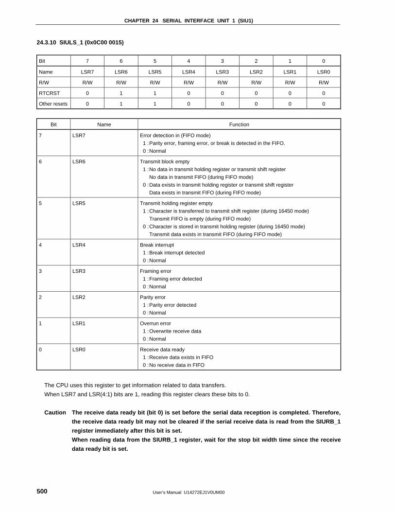
CHAPTER 24 SERIAL INTERFACE UNIT 1 (SIU1)
User’s Manual U14272EJ1V0UM00500
24.3.10 SIULS_1 (0x0C00 0015)
Bit 7 6 5 4 3 2 1 0
Name LSR7 LSR6 LSR5 LSR4 LSR3 LSR2 LSR1 LSR0
R/W R/W R/W R/W R/W R/W R/W R/W R/W
RTCRST 0 1 1 0 0 0 0 0
Other resets 0 1 1 0 0 0 0 0
Bit Name Function
7 LSR7 Error detection in (FIFO mode)
1 :Parity error, framing error, or break is detected in the FIFO.
0 :Normal
6 LSR6 Transmit block empty
1 :No data in transmit holding register or transmit shift register
No data in transmit FIFO (during FIFO mode)
0 :Data exists in transmit holding register or transmit shift register
Data exists in transmit FIFO (during FIFO mode)
5 LSR5 Transmit holding register empty
1 :Character is transferred to transmit shift register (during 16450 mode)
Transmit FIFO is empty (during FIFO mode)
0 :Character is stored in transmit holding register (during 16450 mode)
Transmit data exists in transmit FIFO (during FIFO mode)
4 LSR4 Break interrupt
1 :Break interrupt detected
0 :Normal
3 LSR3 Framing error
1 :Framing error detected
0 :Normal
2 LSR2 Parity error
1 :Parity error detected
0 :Normal
1 LSR1 Overrun error
1 :Overwrite receive data
0 :Normal
0 LSR0 Receive data ready
1 :Receive data exists in FIFO
0 :No receive data in FIFO
The CPU uses this register to get information related to data transfers.
When LSR7 and LSR(4:1) bits are 1, reading this register clears these bits to 0.
Caution The receive data ready bit (bit 0) is set before the serial data reception is completed. Therefore,
the receive data ready bit may not be cleared if the serial receive data is read from the SIURB_1
register immediately after this bit is set.
When reading data from the SIURB_1 register, wait for the stop bit width time since the receive
data ready bit is set.

CHAPTER 24 SERIAL INTERFACE UNIT 1 (SIU1)
User’s Manual U14272EJ1V0UM00 501
LSR7 bit is valid only in FIFO mode, and it indicates always 0 in 16450 mode.
The value of LSR4 bit becomes 1 when the spacing mode (logical 0) is held longer than the time required for
transmission of one word of receive data input (start bit + data bits + parity bit + stop bit).
This bit value returns 0 when the CPU reads the contents of the line status register. When in FIFO mode, if a
break interrupt is detected for one character in the FIFO, the character is regarded as an error character and the CPU
is notified of a break interrupt when that character reaches the highest position in the FIFO.
When a break occurs, one “zero” character is sent to the FIFO. The RxD1 enters marking mode, and when the
next valid start bit is received, the next character can be transmitted.
The value of LSR3 bit becomes 1 when a zero (spacing level) stop bit is detected following the final data bit or
parity bit. This bit value returns to 0 when the CPU reads the contents of the line status register.
When in FIFO mode, if a framing error is detected for one character in the FIFO, the character is regarded as an
error character and the CPU is notified of a framing error when that character reaches the highest position in the
FIFO.
When a framing error occurs, the SIU1 prepares for further synchronization. The next start bit is assumed to be
the cause of the framing error and further data is not accepted until the next start bit has been sampled twice.
The value of LSR2 bit becomes 1 when a parity error is detected. This bit value returns to 0 when the CPU reads
the contents of the line status register.
When in FIFO mode, if a parity error is detected for one character within the FIFO, the character is regarded as an
error character and the CPU is notified of a parity error when that character reaches the highest position in the FIFO.
The value of LSR1 bit becomes 1 when overrun status is detected and returns to 0 when the CPU reads the
contents of the line status register.
When in FIFO mode, if the data exceeds the trigger level as it continues to be transferred to the FIFO, even after
the FIFO becomes full an overrun error will not occur until all characters are stored in the shift register.
The CPU is notified as soon as an overrun error occurs. The characters in the shift register are overwritten and
are not transferred to the FIFO.
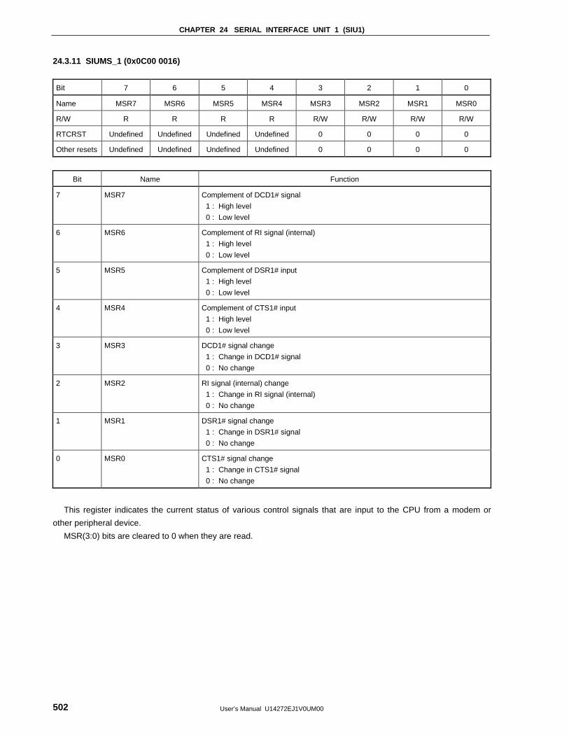
CHAPTER 24 SERIAL INTERFACE UNIT 1 (SIU1)
User’s Manual U14272EJ1V0UM00502
24.3.11 SIUMS_1 (0x0C00 0016)
Bit 7 6 5 4 3 2 1 0
Name MSR7 MSR6 MSR5 MSR4 MSR3 MSR2 MSR1 MSR0
R/W R R R R R/W R/W R/W R/W
RTCRST Undefined Undefined Undefined Undefined 0 0 0 0
Other resets Undefined Undefined Undefined Undefined 0 0 0 0
Bit Name Function
7 MSR7 Complement of DCD1# signal
1 : High level
0 : Low level
6 MSR6 Complement of RI signal (internal)
1 : High level
0 : Low level
5 MSR5 Complement of DSR1# input
1 : High level
0 : Low level
4 MSR4 Complement of CTS1# input
1 : High level
0 : Low level
3 MSR3 DCD1# signal change
1 : Change in DCD1# signal
0 : No change
2 MSR2 RI signal (internal) change
1 : Change in RI signal (internal)
0 : No change
1 MSR1 DSR1# signal change
1 : Change in DSR1# signal
0 : No change
0 MSR0 CTS1# signal change
1 : Change in CTS1# signal
0 : No change
This register indicates the current status of various control signals that are input to the CPU from a modem or
other peripheral device.
MSR(3:0) bits are cleared to 0 when they are read.
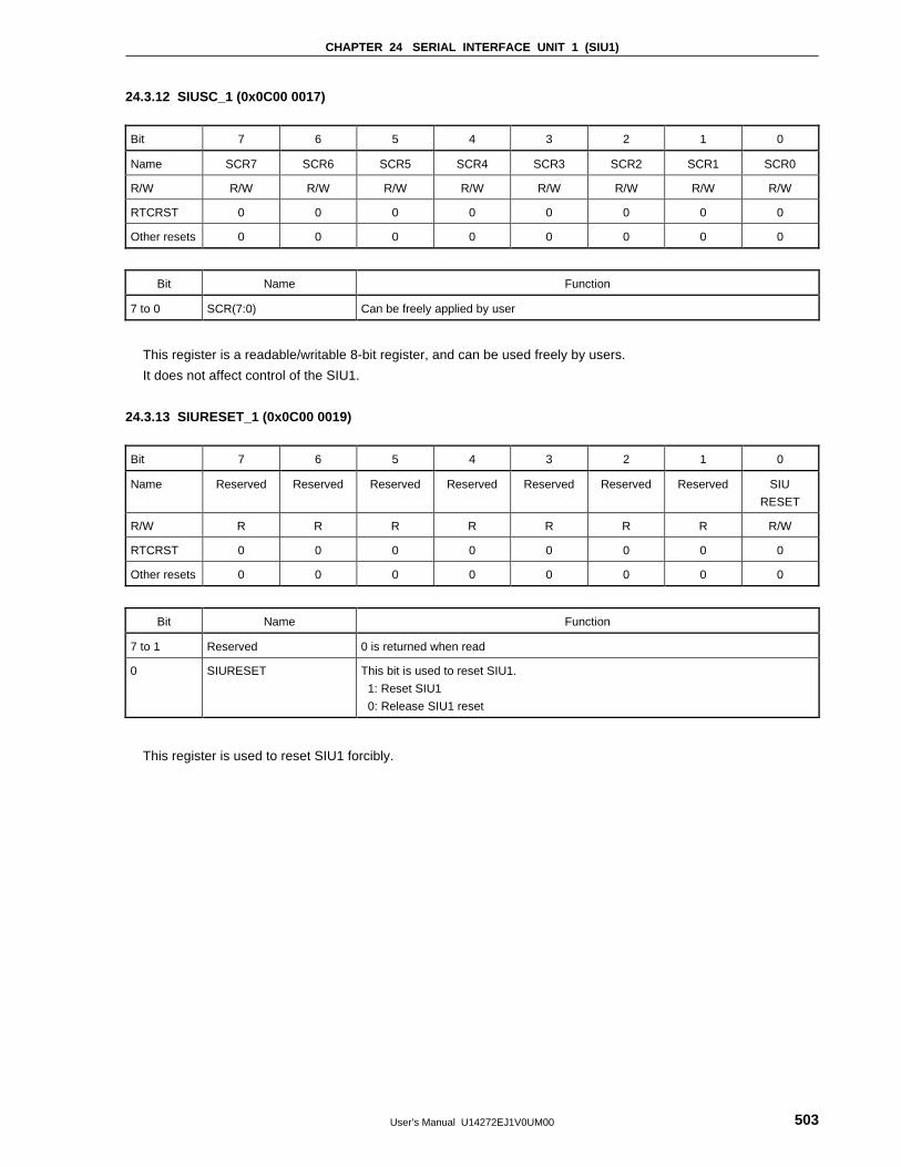
CHAPTER 24 SERIAL INTERFACE UNIT 1 (SIU1)
User’s Manual U14272EJ1V0UM00 503
24.3.12 SIUSC_1 (0x0C00 0017)
Bit 7 6 5 4 3 2 1 0
Name SCR7 SCR6 SCR5 SCR4 SCR3 SCR2 SCR1 SCR0
R/W R/W R/W R/W R/W R/W R/W R/W R/W
RTCRST 0 0 0 0 0 0 0 0
Other resets 0 0 0 0 0 0 0 0
Bit Name Function
7 to 0 SCR(7:0) Can be freely applied by user
This register is a readable/writable 8-bit register, and can be used freely by users.
It does not affect control of the SIU1.
24.3.13 SIURESET_1 (0x0C00 0019)
Bit 7 6 5 4 3 2 1 0
Name Reserved Reserved Reserved Reserved Reserved Reserved Reserved SIU
RESET
R/W R R R R R R R R/W
RTCRST 0 0 0 0 0 0 0 0
Other resets 0 0 0 0 0 0 0 0
Bit Name Function
7 to 1 Reserved 0 is returned when read
0 SIURESET This bit is used to reset SIU1.
1: Reset SIU1
0: Release SIU1 reset
This register is used to reset SIU1 forcibly.
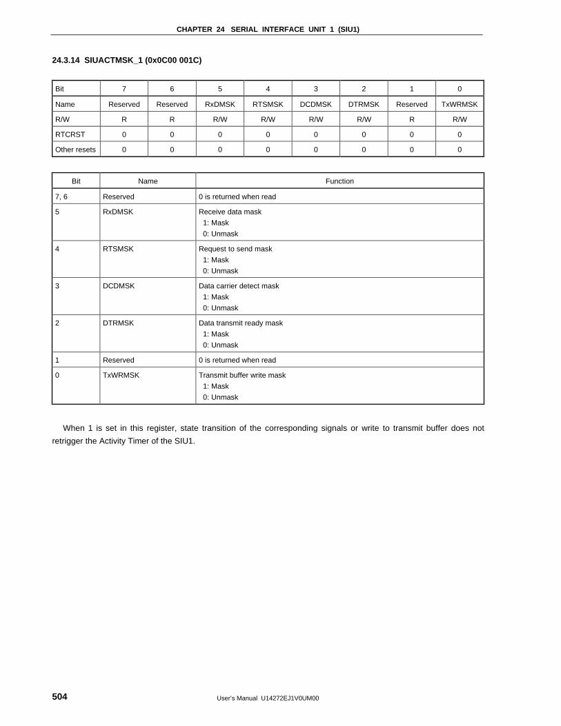
CHAPTER 24 SERIAL INTERFACE UNIT 1 (SIU1)
User’s Manual U14272EJ1V0UM00504
24.3.14 SIUACTMSK_1 (0x0C00 001C)
Bit 7 6 5 4 3 2 1 0
Name Reserved Reserved RxDMSK RTSMSK DCDMSK DTRMSK Reserved TxWRMSK
R/W R R R/W R/W R/W R/W R R/W
RTCRST 0 0 0 0 0 0 0 0
Other resets 0 0 0 0 0 0 0 0
Bit Name Function
7, 6 Reserved 0 is returned when read
5 RxDMSK Receive data mask
1: Mask
0: Unmask
4 RTSMSK Request to send mask
1: Mask
0: Unmask
3 DCDMSK Data carrier detect mask
1: Mask
0: Unmask
2 DTRMSK Data transmit ready mask
1: Mask
0: Unmask
1 Reserved 0 is returned when read
0 TxWRMSK Transmit buffer write mask
1: Mask
0: Unmask
When 1 is set in this register, state transition of the corresponding signals or write to transmit buffer does not
retrigger the Activity Timer of the SIU1.
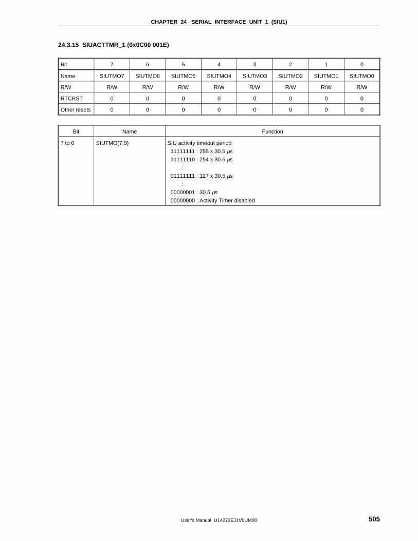
CHAPTER 24 SERIAL INTERFACE UNIT 1 (SIU1)
User’s Manual U14272EJ1V0UM00 505
24.3.15 SIUACTTMR_1 (0x0C00 001E)
Bit 7 6 5 4 3 2 1 0
Name SIUTMO7 SIUTMO6 SIUTMO5 SIUTMO4 SIUTMO3 SIUTMO2 SIUTMO1 SIUTMO0
R/W R/W R/W R/W R/W R/W R/W R/W R/W
RTCRST 0 0 0 0 0 0 0 0
Other resets 0 0 0 0 0 0 0 0
Bit Name Function
7 to 0 SIUTMO(7:0) SIU activity timeout period
11111111 : 255 x 30.5 µs
11111110 : 254 x 30.5 µs
:
01111111 : 127 x 30.5 µs
:
00000001 : 30.5 µs
00000000 : Activity Timer disabled

User’s Manual U14272EJ1V0UM00506
[MEMO]
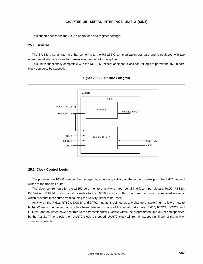
User’s Manual U14272EJ1V0UM00 507
CHAPTER 25 SERIAL INTERFACE UNIT 2 (SIU2)
This chapter describes the SIU2’s operations and register settings.
25.1 General
The SIU2 is a serial interface that conforms to the RS-232-C communication standard and is equipped with two
one-channel interfaces, one for transmission and one for reception.
This unit is functionally compatible with the NS16550 except additional clock control logic to permit the 16650 core
clock source to be stopped.
Figure 25-1. SIU2 Block Diagram
VR4181
UART2
IRDIN/RxD2
IRDOUT/TxD2
RTS2# Activity Timer 2
DTR2#
DCD2#
clk32k
seclk_siu
UART2_clock
SIU2
25.2 Clock Control Logic
The power of the 16550 core can be managed by monitoring activity on the modem status pins, the RxD2 pin, and
writes to the transmit buffer.
The clock control logic for the 16550 core monitors activity on four serial interface input signals; RxD2, RTS2#,
DCD2# and DTR2#. It also monitors writes to the 16550 transmit buffer. Each source has an associated mask bit
which prevents that source from causing the Activity Timer to be reset.
Activity on the RxD2, RTS2#, DCD2# and DTR2# inputs is defined as any change of state (high to low or low to
high). When no unmasked activity has been detected on any of the serial port inputs (RxD2, RTS2#, DCD2# and
DTR2#), and no writes have occurred to the transmit buffer (TXWR) within the programmed time-out period specified
by the Activity Timer block, then UART2_clock is stopped. UART2_clock will remain stopped until any of the activity
sources is detected.
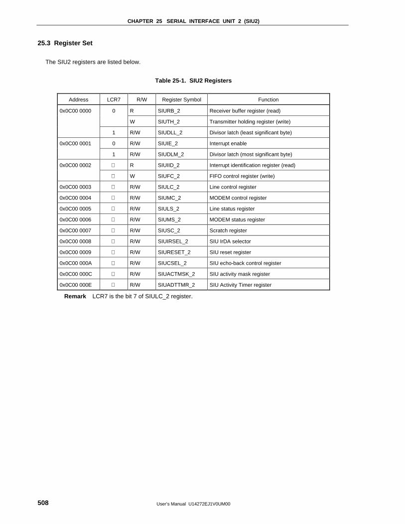
CHAPTER 25 SERIAL INTERFACE UNIT 2 (SIU2)
User’s Manual U14272EJ1V0UM00508
25.3 Register Set
The SIU2 registers are listed below.
Table 25-1. SIU2 Registers
Address LCR7 R/W Register Symbol Function
0x0C00 0000 0 R SIURB_2 Receiver buffer register (read)
W SIUTH_2 Transmitter holding register (write)
1 R/W SIUDLL_2 Divisor latch (least significant byte)
0x0C00 0001 0 R/W SIUIE_2 Interrupt enable
1 R/W SIUDLM_2 Divisor latch (most significant byte)
0x0C00 0002 R SIUIID_2 Interrupt identification register (read)
W SIUFC_2 FIFO control register (write)
0x0C00 0003 R/W SIULC_2 Line control register
0x0C00 0004 R/W SIUMC_2 MODEM control register
0x0C00 0005 R/W SIULS_2 Line status register
0x0C00 0006 R/W SIUMS_2 MODEM status register
0x0C00 0007 R/W SIUSC_2 Scratch register
0x0C00 0008 R/W SIUIRSEL_2 SIU IrDA selector
0x0C00 0009 R/W SIURESET_2 SIU reset register
0x0C00 000A R/W SIUCSEL_2 SIU echo-back control register
0x0C00 000C R/W SIUACTMSK_2 SIU activity mask register
0x0C00 000E R/W SIUADTTMR_2 SIU Activity Timer register
Remark LCR7 is the bit 7 of SIULC_2 register.
CHAPTER 25 SERIAL INTERFACE UNIT 2 (SIU2)
User’s Manual U14272EJ1V0UM00 509
25.3.1 SIURB_2 (0x0C00 0000: LCR7 = 0, Read)
Bit 7 6 5 4 3 2 1 0
Name RXD7 RXD6 RXD5 RXD4 RXD3 RXD2 RXD1 RXD0
R/W R R R R R R R R
RTCRST 0 0 0 0 0 0 0 0
Other resets 0 0 0 0 0 0 0 0
Bit Name Function
7 to 0 RXD(7:0) Serial receive data
This register stores receive data used in serial communications.
To access this register, set LCR7 (bit 7 of SIULC_2 register) to 0.
25.3.2 SIUTH_2 (0x0C00 0000: LCR7 = 0, Write)
Bit 7 6 5 4 3 2 1 0
Name TXD7 TXD6 TXD5 TXD4 TXD3 TXD2 TXD1 TXD0
R/W W W W W W W W W
RTCRST 0 0 0 0 0 0 0 0
Other resets 0 0 0 0 0 0 0 0
Bit Name Function
7 to 0 TXD(7:0) Serial transmit data
This register stores transmit data used in serial communications.
To access this register, set LCR7 (bit 7 of SIULC_2 register) to 0.
25.3.3 SIUDLL_2 (0x0C00 0000: LCR7 = 1)
Bit 7 6 5 4 3 2 1 0
Name DLL7 DLL6 DLL5 DLL4 DLL3 DLL2 DLL1 DLL0
R/W R/W R/W R/W R/W R/W R/W R/W R/W
RTCRST 0 0 0 0 0 0 0 0
Other resets 0 0 0 0 0 0 0 0
Bit Name Function
7 to 0 DLL(7:0) Baud rate generator divisor (low-order byte)
This register is used to set the divisor (division rate) for the baud rate generator.
The data in this register and the upper 8-bit data in SIUDLM_2 register are together handled as 16-bit data.
To access this register, set LCR7 (bit 7 of SIULC_2 register) to 1.
CHAPTER 25 SERIAL INTERFACE UNIT 2 (SIU2)
User’s Manual U14272EJ1V0UM00510
25.3.4 SIUIE_2 (0x0C00 0001: LCR7 = 0)
Bit 7 6 5 4 3 2 1 0
Name Reserved Reserved Reserved Reserved IE3 IE2 IE1 IE0
R/W R R R R R/W R/W R/W R/W
RTCRST 0 0 0 0 0 0 0 0
Other resets 0 0 0 0 0 0 0 0
Bit Name Function
7 to 4 Reserved 0 is returned when read
3 IE3 MODEM status interrupt
1 : Interrupt enable
0 : Interrupt prohibit
2 IE2 Receive status interrupt
1 : Interrupt enable
0 : Interrupt prohibit
1 IE1 Transmitter holding register empty interrupt
1 : Interrupt enable
0 : Interrupt prohibit
0 IE0 Receive data interrupt or timeout interrupt in FIFO mode
1 : Interrupt enable
0 : Interrupt prohibit
This register is used to specify interrupt enable/prohibit settings for the five types of interrupt requests used by
SIU2.
These bits can be used to make the corresponding interrupt request output (INTR) active.
Overall use of interrupt functions can be halted by setting bits 0 to 3 of this register to 0.
When interrupts are prohibited, “pending” is not displayed in the IIR0 bit in the SIUIID_2 register even when the
interrupt condition has been met and INTR output does not become active.
Other functions in the system are not affected even though interrupts are prohibited and the settings in the line
status register (SIULS_2) and MODEM status register (SIUMS_2) are valid.
To access this register, set LCR7 (bit 7 of SIULC_2 register) to 0.
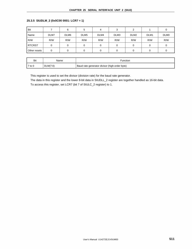
CHAPTER 25 SERIAL INTERFACE UNIT 2 (SIU2)
User’s Manual U14272EJ1V0UM00 511
25.3.5 SIUDLM_2 (0x0C00 0001: LCR7 = 1)
Bit 7 6 5 4 3 2 1 0
Name DLM7 DLM6 DLM5 DLM4 DLM3 DLM2 DLM1 DLM0
R/W R/W R/W R/W R/W R/W R/W R/W R/W
RTCRST 0 0 0 0 0 0 0 0
Other resets 0 0 0 0 0 0 0 0
Bit Name Function
7 to 0 DLM(7:0) Baud rate generator divisor (high-order byte)
This register is used to set the divisor (division rate) for the baud rate generator.
The data in this register and the lower 8-bit data in SIUDLL_2 register are together handled as 16-bit data.
To access this register, set LCR7 (bit 7 of SIULC_2 register) to 1.
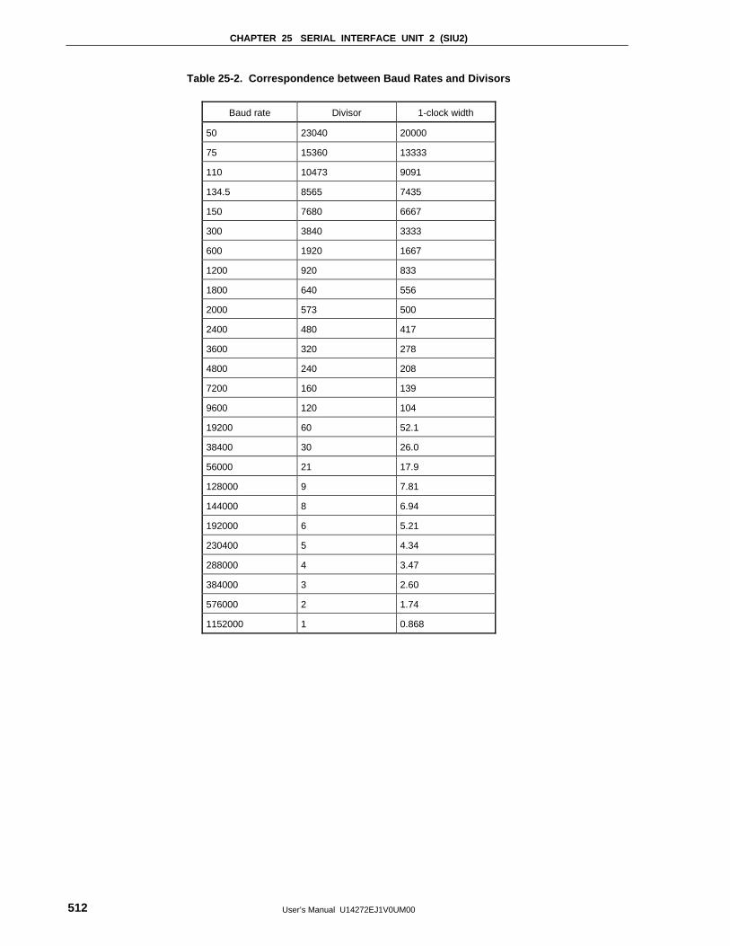
CHAPTER 25 SERIAL INTERFACE UNIT 2 (SIU2)
User’s Manual U14272EJ1V0UM00512
Table 25-2. Correspondence between Baud Rates and Divisors
Baud rate Divisor 1-clock width
50 23040 20000
75 15360 13333
110 10473 9091
134.5 8565 7435
150 7680 6667
300 3840 3333
600 1920 1667
1200 920 833
1800 640 556
2000 573 500
2400 480 417
3600 320 278
4800 240 208
7200 160 139
9600 120 104
19200 60 52.1
38400 30 26.0
56000 21 17.9
128000 9 7.81
144000 8 6.94
192000 6 5.21
230400 5 4.34
288000 4 3.47
384000 3 2.60
576000 2 1.74
1152000 1 0.868

CHAPTER 25 SERIAL INTERFACE UNIT 2 (SIU2)
User’s Manual U14272EJ1V0UM00 513
25.3.6 SIUIID_2 (0x0C00 0002: Read)
Bit 7 6 5 4 3 2 1 0
Name IIR7 IIR6 Reserved Reserved IIR3 IIR2 IIR1 IIR0
R/W R R R R R R R R
RTCRST 0 0 0 0 0 0 0 1
Other resets 0 0 0 0 0 0 0 1
Bit Name Function
7, 6 IIR(7:6) Becomes 11 when FCR0 = 1
5, 4 Reserved 0 is returned when read
3 IIR3 Pending character timeout interrupt (in FIFO mode)
1 : No pending interrupt
0 : Pending interrupt
2, 1 IIR(2:1) Indicates the priority level of pending interrupt.
See the following table.
0 IIR0 Pending interrupts
1 : No pending interrupt
0 : Pending interrupt
This register indicates priority levels for interrupts and existence of pending interrupt.
From highest to lowest priority, these interrupts are receive line status, receive data ready, character timeout,
transmit holding register empty, and MODEM status.
The contents of IIR3 bit are valid only in FIFO mode, and it is always 0 in 16450 mode.
IIR2 bit becomes 1 when IIR3 bit is set to 1.

CHAPTER 25 SERIAL INTERFACE UNIT 2 (SIU2)
User’s Manual U14272EJ1V0UM00514
Table 25-3. Interrupt Function
SIUIID_2 register Interrupt set/reset function
Bit 3 Note
Bit 2 Bit 1 Priority level Interrupt type Interrupt source Interrupt reset control
0 1 1 Highest (1st) Receive line
status
Overrun error, parity error, framing error,
or break interrupt
Read line status register
0 1 0 2nd Receive data
ready
Receive data exists or has reached the
trigger level.
Read the receive buffer
register or lower trigger
level via FIFO.
1 1 0 2nd Character
timeout
During the time period for the four most
recent characters, not one character has
been read from the receive FIFO nor has
a character been input to the receive
FIFO. During this period, at least one
character has been held in the receive
FIFO.
Read receive buffer
register
0 0 1 3rd Transmit
holding
register
empty
Transmit register is empty Read IIR (if it is the
interrupt source) or write
to transmit holding
register
0 0 0 4th MODEM
status
CTS2#, DSR2#, or DCD2# Read MODEM status
register
Note FIFO mode only.
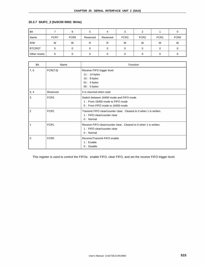
CHAPTER 25 SERIAL INTERFACE UNIT 2 (SIU2)
User’s Manual U14272EJ1V0UM00 515
25.3.7 SIUFC_2 (0x0C00 0002: Write)
Bit 7 6 5 4 3 2 1 0
Name FCR7 FCR6 Reserved Reserved FCR3 FCR2 FCR1 FCR0
R/W W W R R W W W W
RTCRST 0 0 0 0 0 0 0 0
Other resets 0 0 0 0 0 0 0 0
Bit Name Function
7, 6 FCR(7:6) Receive FIFO trigger level
11 : 14 bytes
10 : 8 bytes
01 : 4 bytes
00 : 0 bytes
5, 4 Reserved 0 is returned when read
3 FCR3 Switch between 16450 mode and FIFO mode
1 : From 16450 mode to FIFO mode
0 : From FIFO mode to 16450 mode
2 FCR2 Transmit FIFO clear/counter clear. Cleared to 0 when 1 is written.
1 : FIFO clear/counter clear
0 : Normal
1 FCR1 Receive FIFO clear/counter clear. Cleared to 0 when 1 is written.
1 : FIFO clear/counter clear
0 : Normal
0 FCR0 Receive/Transmit FIFO enable
1 : Enable
0 : Disable
This register is used to control the FIFOs: enable FIFO, clear FIFO, and set the receive FIFO trigger level.

CHAPTER 25 SERIAL INTERFACE UNIT 2 (SIU2)
User’s Manual U14272EJ1V0UM00516
• FIFO interrupt modes
When receive FIFO is enabled and receive interrupts are enabled, receive interrupts can occur as described
below.
1. When the FIFO is reached to the specified trigger level, a receive data ready interrupt occurs to inform the
CPU.
This interrupt is cleared when the FIFO goes below the trigger level.
2. When the FIFO is reached to the specified trigger level, the SIUIID_2 register indicates a receive data
ready interrupt.
As with the interrupt above, SUIID_2 register is cleared when the FIFO goes below the trigger level.
3. Receive line status interrupts are assigned a higher priority level than are receive data ready interrupts.
4. When characters are transferred from the shift register to the receive FIFO, 1 is set to the LSR0 bit.
The value of this bit returns to 0 when the FIFO becomes empty.
When receive FIFO is enabled and receive interrupts are enabled, receive FIFO timeout interrupts can occur as
described below.
1. The following are conditions under which FIFO timeout interrupts occur.
• At least one character is being stored in the FIFO.
• The time required for sending four characters has elapsed since the serial reception of the last
character (includes the time for two stop bits in cases where a stop bit has been specified).
• The time required for sending four characters has elapsed since the CPU last accessed the FIFO.
The time between receiving the last character and issuing a timeout interrupt is a maximum of 160 ms
when operating at 300 baud and receiving 12-bit data.
2. The transfer time for a character is calculated based on the baud rate clock for reception (internal) input
as clock signals (which is why the elapsed time is in proportion to the baud rate).
3. Once a timeout interrupt has occurred, the timeout interrupt is cleared and the timer is reset as soon as
the CPU reads one character from the receive FIFO.
4. If no timeout interrupt has occurred, the timer is reset when a new character is received or when the CPU
reads the receive FIFO.

CHAPTER 25 SERIAL INTERFACE UNIT 2 (SIU2)
User’s Manual U14272EJ1V0UM00 517
When transmit FIFO is enabled and transmit interrupts are enabled, transmit interrupts can occur as described
below.
1. When the transmit FIFO becomes empty, a transmit holding register empty interrupt occurs.
This interrupt is cleared when a character is written to the transmit holding register (from one to 16
characters can be written to the transmit FIFO during servicing of this interrupt), or when interrupt ID
register (SIUIID_2) is read.
2. If there are not at least two bytes of character data in the transmit FIFO between one time when LSR5 = 1
(transmit FIFO is empty) and the next time when LSR5 = 1, empty transmit FIFO status is reported to the
IIR bits after a delay period calculated as “the time for one character − the time for the last stop bit(s)”.
When transmit interrupts are enabled, the first transmit interrupt that occurs after the FCR0 (FIFO enable
bit) is overwritten is indicated immediately.
The priority level of the character timeout interrupt and receive FIFO trigger level interrupt is the same as that of
the receive data ready interrupt.
The priority level of the transmit FIFO empty interrupt is the same as that of the transmit holding register empty
interrupt.
Whether data to be transmitted exists or not in the transmit FIFO and the transmit shift register, check the
transmit block empty bit (bit 6) of the SIULS_2 register. It cannot be checked by the transmit holding register
empty bit (bit 5) of the SIULS_2 register, because this bit is used to check whether data to be transferred exists
or not in the transmit FIFO. Therefore, this bit cannot check if there is data in the transmit shift register.
• FIFO polling mode
When FCR0 = 1 (FIFO is enabled), if the value of any or all of the interrupt enable register (SIUIE_2) bits 3 to 0
becomes 0, SIU2 enters FIFO polling mode. Because the transmit block and receive blocks are controlled
separately, polling mode can be set for either or both blocks.
When in this mode, the status of the transmit block and/or receive block can be checked by reading the line
status register (SIULS_2) via a user program.
When in the FIFO polling mode, there is no notification when the trigger level is reached or when a timeout
occurs, but the receive FIFO and transmit FIFO can still store characters as they normally do.

CHAPTER 25 SERIAL INTERFACE UNIT 2 (SIU2)
User’s Manual U14272EJ1V0UM00518
25.3.8 SIULC_2 (0x0C00 0003)
Bit 7 6 5 4 3 2 1 0
Name LCR7 LCR6 LCR5 LCR4 LCR3 LCR2 LCR1 LCR0
R/W R/W R/W R/W R/W R/W R/W R/W R/W
RTCRST 0 0 0 0 0 0 0 0
Other resets 0 0 0 0 0 0 0 0
Bit Name Function
7 LCR7 Divisor latch access bit specification (DLAB)
1 : Divisor latch access
0 : Receive buffer, transmit holding register, interrupt enable register
6 LCR6 Break control
1 : Set break
0 : Clear break
5 LCR5 Parity fixing
1 : Fixed parity
0 : Parity not fixed
4 LCR4 Parity setting
1 : Set one bit as even bit
0 : Set one bit as odd bit
3 LCR3 Parity enable
1 : Create parity (during transmission) or check parity (during reception)
0 : No parity (during transmission) or no checking (during reception)
2 LCR2 Stop bit specification
1 : 1.5 bits (character length is 5 bits)
2 bits (character length is 6, 7, or 8 bits)
0 : 1 bit
1, 0 LCR(1:0) Specifies the length of one character (number of bits)
11 : 8 bits
10 : 7 bits
01 : 6 bits
00 : 5 bits
This register is used to specify the format for asynchronous communication and exchange and to set the divisor
latch access bit.
Bit 6 is used to send the break status to the receive side’s UART. When bit 6 = 1, the serial output (TxD2) is
forcibly set to the spacing (0) state.
The setting of bit 5 becomes valid according to settings in bits 4 and 3.
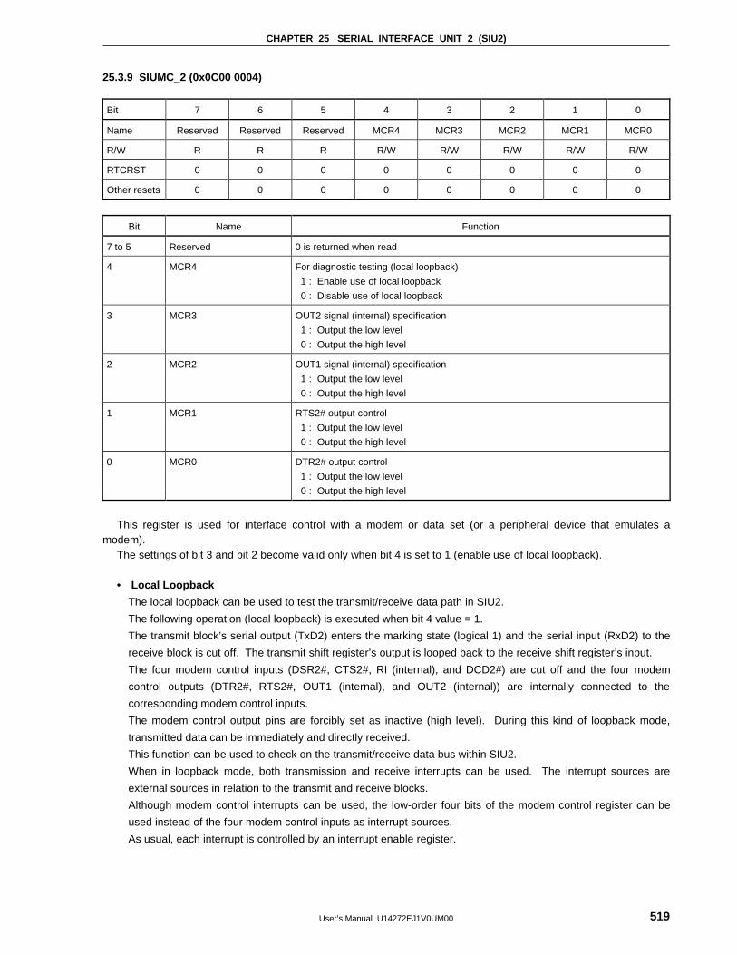
CHAPTER 25 SERIAL INTERFACE UNIT 2 (SIU2)
User’s Manual U14272EJ1V0UM00 519
25.3.9 SIUMC_2 (0x0C00 0004)
Bit 7 6 5 4 3 2 1 0
Name Reserved Reserved Reserved MCR4 MCR3 MCR2 MCR1 MCR0
R/W R R R R/W R/W R/W R/W R/W
RTCRST 0 0 0 0 0 0 0 0
Other resets 0 0 0 0 0 0 0 0
Bit Name Function
7 to 5 Reserved 0 is returned when read
4 MCR4 For diagnostic testing (local loopback)
1 : Enable use of local loopback
0 : Disable use of local loopback
3 MCR3 OUT2 signal (internal) specification
1 : Output the low level
0 : Output the high level
2 MCR2 OUT1 signal (internal) specification
1 : Output the low level
0 : Output the high level
1 MCR1 RTS2# output control
1 : Output the low level
0 : Output the high level
0 MCR0 DTR2# output control
1 : Output the low level
0 : Output the high level
This register is used for interface control with a modem or data set (or a peripheral device that emulates amodem).
The settings of bit 3 and bit 2 become valid only when bit 4 is set to 1 (enable use of local loopback).
• Local Loopback
The local loopback can be used to test the transmit/receive data path in SIU2.
The following operation (local loopback) is executed when bit 4 value = 1.
The transmit block’s serial output (TxD2) enters the marking state (logical 1) and the serial input (RxD2) to the
receive block is cut off. The transmit shift register’s output is looped back to the receive shift register’s input.
The four modem control inputs (DSR2#, CTS2#, RI (internal), and DCD2#) are cut off and the four modem
control outputs (DTR2#, RTS2#, OUT1 (internal), and OUT2 (internal)) are internally connected to the
corresponding modem control inputs.
The modem control output pins are forcibly set as inactive (high level). During this kind of loopback mode,
transmitted data can be immediately and directly received.
This function can be used to check on the transmit/receive data bus within SIU2.
When in loopback mode, both transmission and receive interrupts can be used. The interrupt sources are
external sources in relation to the transmit and receive blocks.
Although modem control interrupts can be used, the low-order four bits of the modem control register can be
used instead of the four modem control inputs as interrupt sources.
As usual, each interrupt is controlled by an interrupt enable register.

CHAPTER 25 SERIAL INTERFACE UNIT 2 (SIU2)
User’s Manual U14272EJ1V0UM00520
25.3.10 SIULS_2 (0x0C00 0005)
Bit 7 6 5 4 3 2 1 0
Name LSR7 LSR6 LSR5 LSR4 LSR3 LSR2 LSR1 LSR0
R/W R/W R/W R/W R/W R/W R/W R/W R/W
RTCRST 0 1 1 0 0 0 0 0
Other resets 0 1 1 0 0 0 0 0
Bit Name Function
7 LSR7 Error detection in (FIFO mode)
1 :Parity error, framing error, or break is detected in the FIFO.
0 :Normal
6 LSR6 Transmit block empty
1 :No data in transmit holding register or transmit shift register
No data in transmit FIFO (during FIFO mode)
0 :Data exists in transmit holding register or transmit shift register
Data exists in transmit FIFO (during FIFO mode)
5 LSR5 Transmit holding register empty
1 :Character is transferred to transmit shift register (during 16450 mode)
Transmit FIFO is empty (during FIFO mode)
0 :Character is stored in transmit holding register (during 16450 mode)
Transmit data exists in transmit FIFO (during FIFO mode)
4 LSR4 Break interrupt
1 :Break interrupt detected
0 :Normal
3 LSR3 Framing error
1 :Framing error detected
0 :Normal
2 LSR2 Parity error
1 :Parity error detected
0 :Normal
1 LSR1 Overrun error
1 :Overwrite receive data
0 :Normal
0 LSR0 Receive data ready
1 :Receive data exists in FIFO
0 :No receive data in FIFO
The CPU uses this register to get information related to data transfers.
When LSR7 and LSR(4:1) bits are 1, reading this register clears these bits to 0.
Caution The receive data ready bit (bit 0) is set before the serial data reception is completed. Therefore,
the receive data ready bit may not be cleared if the serial receive data is read from the SIURB_2
register immediately after this bit is set.
When reading data from the SIURB_2 register, wait for the stop bit width time since the receive
data ready bit is set.
CHAPTER 25 SERIAL INTERFACE UNIT 2 (SIU2)
User’s Manual U14272EJ1V0UM00 521
LSR7 bit is valid only in FIFO mode, and it indicates always 0 in 16450 mode.
The value of LSR4 bit becomes 1 when the spacing mode (logical 0) is held longer than the time required for
transmission of one word of receive data input (start bit + data bits + parity bit + stop bit).
This bit value returns 0 when the CPU reads the contents of the line status register. When in FIFO mode, if a
break interrupt is detected for one character in the FIFO, the character is regarded as an error character and the CPU
is notified of a break interrupt when that character reaches the highest position in the FIFO.
When a break occurs, one “zero” character is sent to the FIFO. The RxD2 enters marking mode, and when the
next valid start bit is received, the next character can be transmitted.
The value of LSR3 bit becomes 1 when a zero (spacing level) stop bit is detected following the final data bit or
parity bit. This bit value returns to 0 when the CPU reads the contents of the line status register.
When in FIFO mode, if a framing error is detected for one character in the FIFO, the character is regarded as an
error character and the CPU is notified of a framing error when that character reaches the highest position in the
FIFO.
When a framing error occurs, the SIU2 prepares for further synchronization. The next start bit is assumed to be
the cause of the framing error and further data is not accepted until the next start bit has been sampled twice.
The value of LSR2 bit becomes 1 when a parity error is detected. This bit value returns to 0 when the CPU reads
the contents of the line status register.
When in FIFO mode, if a parity error is detected for one character within the FIFO, the character is regarded as an
error character and the CPU is notified of a parity error when that character reaches the highest position in the FIFO.
The value of LSR1 bit becomes 1 when overrun status is detected and returns to 0 when the CPU reads the
contents of the line status register.
When in FIFO mode, if the data exceeds the trigger level as it continues to be transferred to the FIFO, even after
the FIFO becomes full an overrun error will not occur until all characters are stored in the shift register.
The CPU is notified as soon as an overrun error occurs. The characters in the shift register are overwritten and
are not transferred to the FIFO.

CHAPTER 25 SERIAL INTERFACE UNIT 2 (SIU2)
User’s Manual U14272EJ1V0UM00522
25.3.11 SIUMS_2 (0x0C00 0006)
Bit 7 6 5 4 3 2 1 0
Name MSR7 MSR6 MSR5 MSR4 MSR3 MSR2 MSR1 MSR0
R/W R R R R R/W R/W R/W R/W
RTCRST Undefined Undefined Undefined Undefined 0 0 0 0
Other resets Undefined Undefined Undefined Undefined 0 0 0 0
Bit Name Function
7 MSR7 Complement of DCD2# signal
1 : High level
0 : Low level
6 MSR6 Complement of RI signal (internal)
1 : High level
0 : Low level
5 MSR5 Complement of DSR2# input
1 : High level
0 : Low level
4 MSR4 Complement of CTS2# input
1 : High level
0 : Low level
3 MSR3 DCD2# signal change
1 : Change in DCD2# signal
0 : No change
2 MSR2 RI signal (internal) change
1 : Change in RI signal (internal)
0 : No change
1 MSR1 DSR2# signal change
1 : Change in DSR2# signal
0 : No change
0 MSR0 CTS2# signal change
1 : Change in CTS2# signal
0 : No change
This register indicates the current status of various control signals that are input to the CPU from a modem or
other peripheral device.
MSR(3:0) bits are cleared to 0 when they are read.
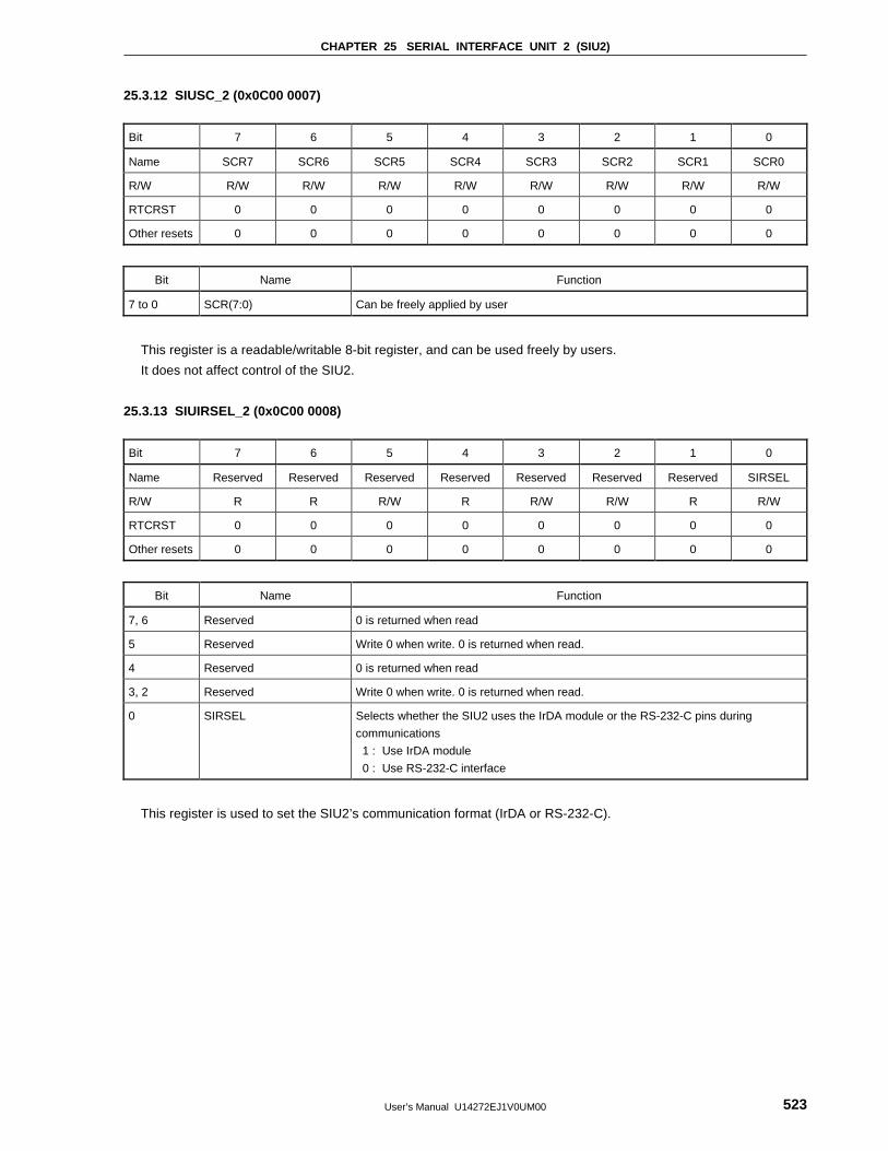
CHAPTER 25 SERIAL INTERFACE UNIT 2 (SIU2)
User’s Manual U14272EJ1V0UM00 523
25.3.12 SIUSC_2 (0x0C00 0007)
Bit 7 6 5 4 3 2 1 0
Name SCR7 SCR6 SCR5 SCR4 SCR3 SCR2 SCR1 SCR0
R/W R/W R/W R/W R/W R/W R/W R/W R/W
RTCRST 0 0 0 0 0 0 0 0
Other resets 0 0 0 0 0 0 0 0
Bit Name Function
7 to 0 SCR(7:0) Can be freely applied by user
This register is a readable/writable 8-bit register, and can be used freely by users.
It does not affect control of the SIU2.
25.3.13 SIUIRSEL_2 (0x0C00 0008)
Bit 7 6 5 4 3 2 1 0
Name Reserved Reserved Reserved Reserved Reserved Reserved Reserved SIRSEL
R/W R R R/W R R/W R/W R R/W
RTCRST 0 0 0 0 0 0 0 0
Other resets 0 0 0 0 0 0 0 0
Bit Name Function
7, 6 Reserved 0 is returned when read
5 Reserved Write 0 when write. 0 is returned when read.
4 Reserved 0 is returned when read
3, 2 Reserved Write 0 when write. 0 is returned when read.
0 SIRSEL Selects whether the SIU2 uses the IrDA module or the RS-232-C pins during
communications
1 : Use IrDA module
0 : Use RS-232-C interface
This register is used to set the SIU2’s communication format (IrDA or RS-232-C).
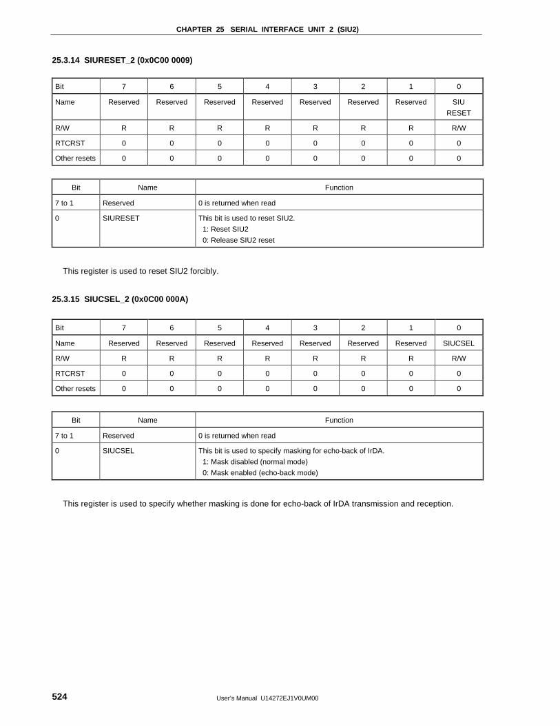
CHAPTER 25 SERIAL INTERFACE UNIT 2 (SIU2)
User’s Manual U14272EJ1V0UM00524
25.3.14 SIURESET_2 (0x0C00 0009)
Bit 7 6 5 4 3 2 1 0
Name Reserved Reserved Reserved Reserved Reserved Reserved Reserved SIU
RESET
R/W R R R R R R R R/W
RTCRST 0 0 0 0 0 0 0 0
Other resets 0 0 0 0 0 0 0 0
Bit Name Function
7 to 1 Reserved 0 is returned when read
0 SIURESET This bit is used to reset SIU2.
1: Reset SIU2
0: Release SIU2 reset
This register is used to reset SIU2 forcibly.
25.3.15 SIUCSEL_2 (0x0C00 000A)
Bit 7 6 5 4 3 2 1 0
Name Reserved Reserved Reserved Reserved Reserved Reserved Reserved SIUCSEL
R/W R R R R R R R R/W
RTCRST 0 0 0 0 0 0 0 0
Other resets 0 0 0 0 0 0 0 0
Bit Name Function
7 to 1 Reserved 0 is returned when read
0 SIUCSEL This bit is used to specify masking for echo-back of IrDA.
1: Mask disabled (normal mode)
0: Mask enabled (echo-back mode)
This register is used to specify whether masking is done for echo-back of IrDA transmission and reception.
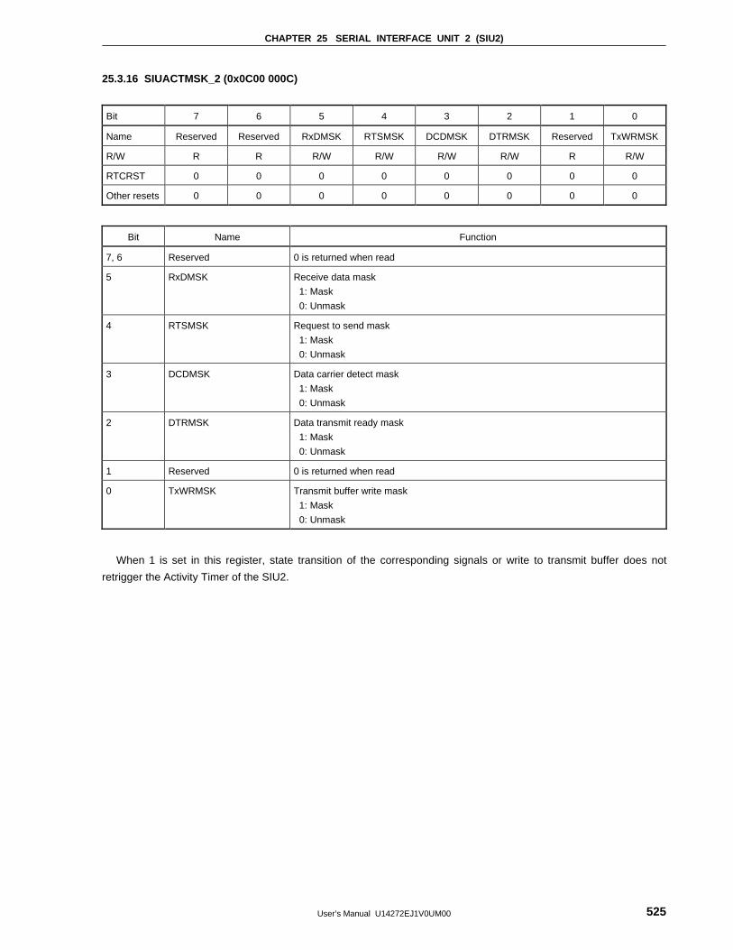
CHAPTER 25 SERIAL INTERFACE UNIT 2 (SIU2)
User’s Manual U14272EJ1V0UM00 525
25.3.16 SIUACTMSK_2 (0x0C00 000C)
Bit 7 6 5 4 3 2 1 0
Name Reserved Reserved RxDMSK RTSMSK DCDMSK DTRMSK Reserved TxWRMSK
R/W R R R/W R/W R/W R/W R R/W
RTCRST 0 0 0 0 0 0 0 0
Other resets 0 0 0 0 0 0 0 0
Bit Name Function
7, 6 Reserved 0 is returned when read
5 RxDMSK Receive data mask
1: Mask
0: Unmask
4 RTSMSK Request to send mask
1: Mask
0: Unmask
3 DCDMSK Data carrier detect mask
1: Mask
0: Unmask
2 DTRMSK Data transmit ready mask
1: Mask
0: Unmask
1 Reserved 0 is returned when read
0 TxWRMSK Transmit buffer write mask
1: Mask
0: Unmask
When 1 is set in this register, state transition of the corresponding signals or write to transmit buffer does not
retrigger the Activity Timer of the SIU2.
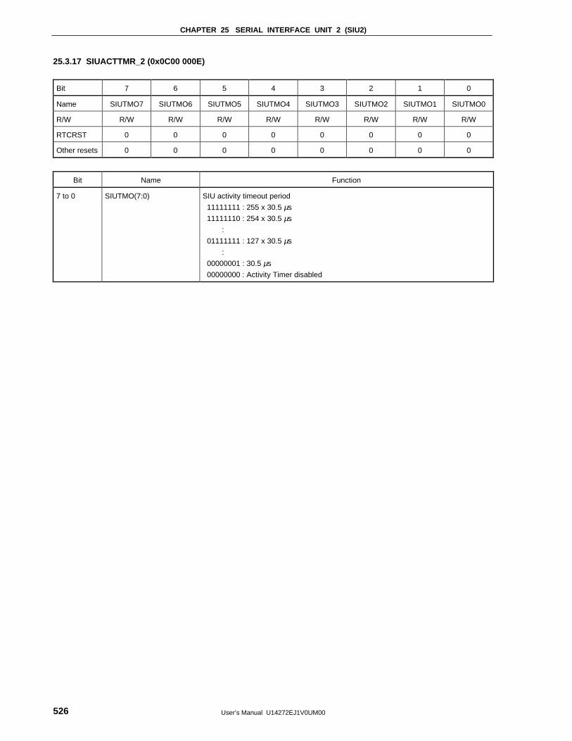
CHAPTER 25 SERIAL INTERFACE UNIT 2 (SIU2)
User’s Manual U14272EJ1V0UM00526
25.3.17 SIUACTTMR_2 (0x0C00 000E)
Bit 7 6 5 4 3 2 1 0
Name SIUTMO7 SIUTMO6 SIUTMO5 SIUTMO4 SIUTMO3 SIUTMO2 SIUTMO1 SIUTMO0
R/W R/W R/W R/W R/W R/W R/W R/W R/W
RTCRST 0 0 0 0 0 0 0 0
Other resets 0 0 0 0 0 0 0 0
Bit Name Function
7 to 0 SIUTMO(7:0) SIU activity timeout period
11111111 : 255 x 30.5 µs
11111110 : 254 x 30.5 µs
:
01111111 : 127 x 30.5 µs
:
00000001 : 30.5 µs
00000000 : Activity Timer disabled
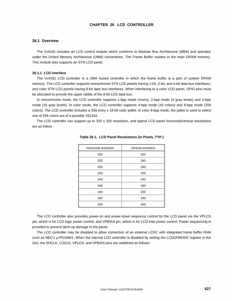
User’s Manual U14272EJ1V0UM00 527
CHAPTER 26 LCD CONTROLLER
26.1 Overview
The VR4181 includes an LCD control module which conforms to Modular Bus Architecture (MBA) and operates
under the United Memory Architecture (UMA) conventions. The Frame Buffer resides in the main DRAM memory.
This module also supports an STN LCD panel.
26.1.1 LCD interface
The VR4181 LCD controller is a UMA based controller in which the frame buffer is a part of system DRAM
memory. The LCD controller supports monochrome STN LCD panels having 1-bit, 2-bit, and 4-bit data bus interfaces,
and color STN LCD panels having 8-bit data bus interfaces. When interfacing to a color LCD panel, GPIO pins must
be allocated to provide the upper nibble of the 8-bit LCD data bus.
In monochrome mode, the LCD controller supports 1-bpp mode (mono), 2-bpp mode (4 gray levels) and 4-bpp
mode (16 gray levels). In color mode, the LCD controller supports 4-bpp mode (16 colors) and 8-bpp mode (256
colors). The LCD controller includes a 256-entry x 18-bit color pallet. In color 8-bpp mode, the pallet is used to select
one of 256 colors out of a possible 261244.
The LCD controller can support up to 320 x 320 resolution, and typical LCD panel horizontal/vertical resolutions
are as follow.
Table 26-1. LCD Panel Resolutions (in Pixels, TYP.)
Horizontal resolution Vertical resolution
320 320
320 240
320 160
240 320
240 240
240 160
160 320
160 240
160 160
The LCD controller also provides power-on and power-down sequence control for the LCD panel via the VPLCD
pin, which is for LCD logic power control, and VPBIAS pin, which is for LCD bias power control. Power sequencing is
provided to prevent latch-up damage to the panel.
The LCD controller may be disabled to allow connection of an external LCDC with integrated frame buffer RAM
such as NEC’s µ PD16661. When the internal LCD controller is disabled by setting the LCDGPMODE register in the
GIU, the SHCLK, LOCLK, VPLCD, and VPBIAS pins are redefined as follows:
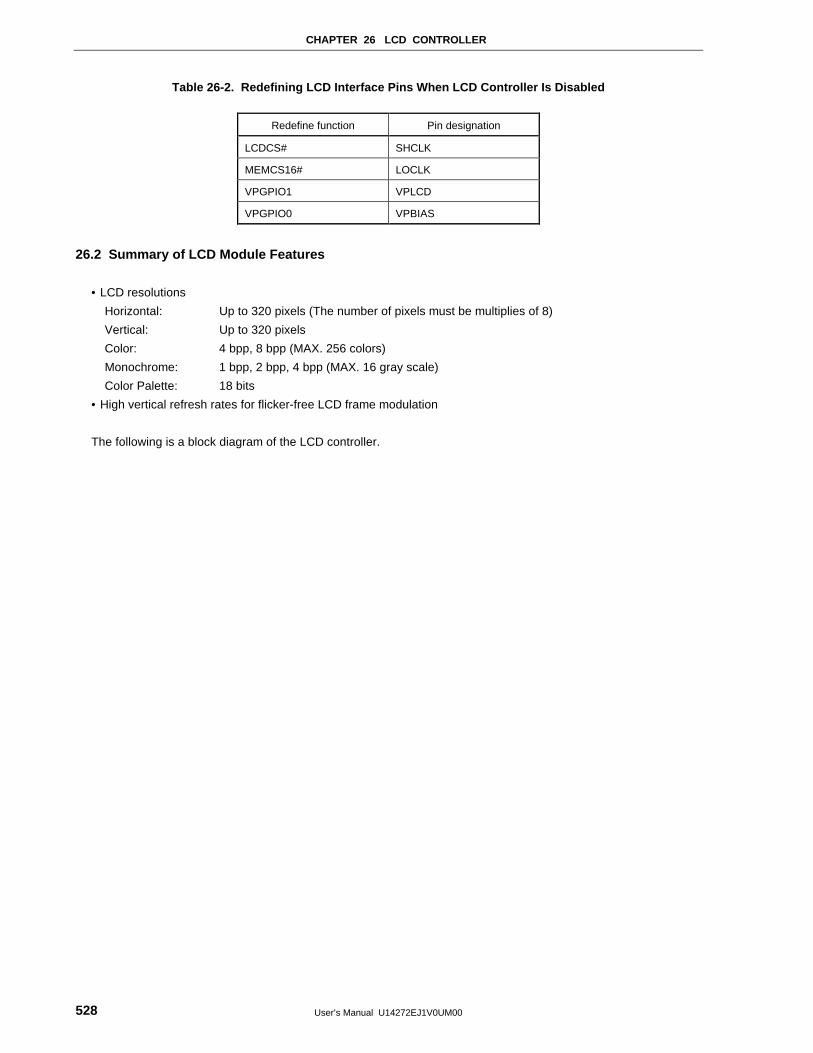
CHAPTER 26 LCD CONTROLLER
User’s Manual U14272EJ1V0UM00528
Table 26-2. Redefining LCD Interface Pins When LCD Controller Is Disabled
Redefine function Pin designation
LCDCS# SHCLK
MEMCS16# LOCLK
VPGPIO1 VPLCD
VPGPIO0 VPBIAS
26.2 Summary of LCD Module Features
• LCD resolutions
Horizontal: Up to 320 pixels (The number of pixels must be multiplies of 8)
Vertical: Up to 320 pixels
Color: 4 bpp, 8 bpp (MAX. 256 colors)
Monochrome: 1 bpp, 2 bpp, 4 bpp (MAX. 16 gray scale)
Color Palette: 18 bits
• High vertical refresh rates for flicker-free LCD frame modulation
The following is a block diagram of the LCD controller.
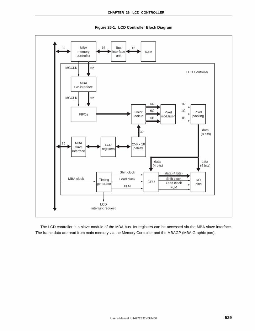
CHAPTER 26 LCD CONTROLLER
User’s Manual U14272EJ1V0UM00 529
Figure 26-1. LCD Controller Block Diagram
MBAmemorycontroller
Businterface
unitRAM
FIFOsColor
lookupPixel
modulation
MBAslave
interface
LCDregisters
256 x 18palette
Timinggenerator GPU I/O
pins
Pixelpacking
MBAGP interface
32 16 16
32MGCLK
6R
6G
6B
1R
1G
1B
Shift clock
Load clock
FLM
32
32
32MGCLK
MBA clock
LCDinterrupt request
data (4 bits)
Shift clockLoad clock
FLM
data (8 bits)
data (4 bits)
data (4 bits)
LCD Controller
The LCD controller is a slave module of the MBA bus. Its registers can be accessed via the MBA slave interface.
The frame data are read from main memory via the Memory Controller and the MBAGP (MBA Graphic port).
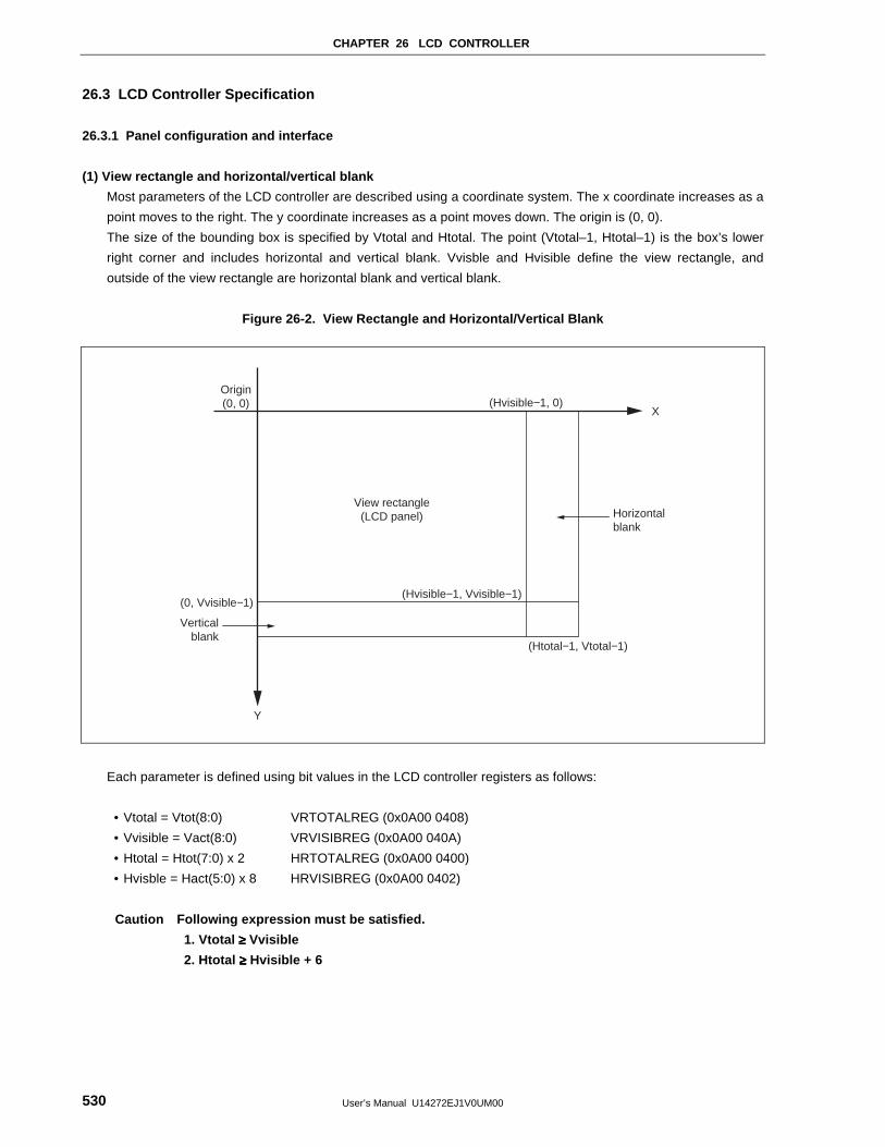
CHAPTER 26 LCD CONTROLLER
User’s Manual U14272EJ1V0UM00530
26.3 LCD Controller Specification
26.3.1 Panel configuration and interface
(1) View rectangle and horizontal/vertical blank
Most parameters of the LCD controller are described using a coordinate system. The x coordinate increases as a
point moves to the right. The y coordinate increases as a point moves down. The origin is (0, 0).
The size of the bounding box is specified by Vtotal and Htotal. The point (Vtotal–1, Htotal–1) is the box’s lower
right corner and includes horizontal and vertical blank. Vvisble and Hvisible define the view rectangle, and
outside of the view rectangle are horizontal blank and vertical blank.
Figure 26-2. View Rectangle and Horizontal/Vertical Blank
Origin(0, 0) (Hvisible−1, 0)
(Htotal−1, Vtotal−1)
View rectangle(LCD panel)
(Hvisible−1, Vvisible−1)(0, Vvisible−1)
Vertical blank
Y
X
Horizontalblank
Each parameter is defined using bit values in the LCD controller registers as follows:
• Vtotal = Vtot(8:0) VRTOTALREG (0x0A00 0408)
• Vvisible = Vact(8:0) VRVISIBREG (0x0A00 040A)
• Htotal = Htot(7:0) x 2 HRTOTALREG (0x0A00 0400)
• Hvisble = Hact(5:0) x 8 HRVISIBREG (0x0A00 0402)
Caution Following expression must be satisfied.
1. Vtotal ≥≥≥≥ Vvisible
2. Htotal ≥≥≥≥ Hvisible + 6
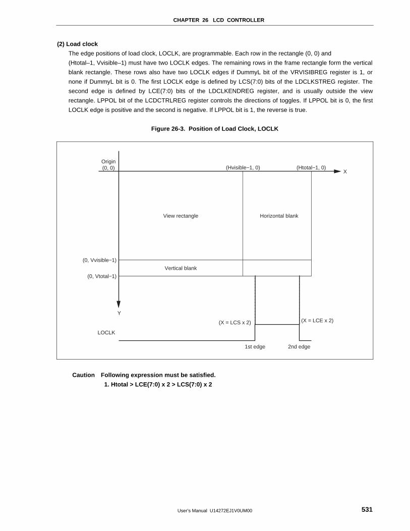
CHAPTER 26 LCD CONTROLLER
User’s Manual U14272EJ1V0UM00 531
(2) Load clock
The edge positions of load clock, LOCLK, are programmable. Each row in the rectangle (0, 0) and
(Htotal–1, Vvisible–1) must have two LOCLK edges. The remaining rows in the frame rectangle form the vertical
blank rectangle. These rows also have two LOCLK edges if DummyL bit of the VRVISIBREG register is 1, or
none if DummyL bit is 0. The first LOCLK edge is defined by LCS(7:0) bits of the LDCLKSTREG register. The
second edge is defined by LCE(7:0) bits of the LDCLKENDREG register, and is usually outside the view
rectangle. LPPOL bit of the LCDCTRLREG register controls the directions of toggles. If LPPOL bit is 0, the first
LOCLK edge is positive and the second is negative. If LPPOL bit is 1, the reverse is true.
Figure 26-3. Position of Load Clock, LOCLK
Origin(0, 0) (Hvisible−1, 0) (Htotal−1, 0)
View rectangle
LOCLK
(0, Vvisible−1)
Vertical blank
Y
X
Horizontal blank
(0, Vtotal−1)
(X = LCS x 2)
1st edge 2nd edge
(X = LCE x 2)
Caution Following expression must be satisfied.
1. Htotal > LCE(7:0) x 2 > LCS(7:0) x 2
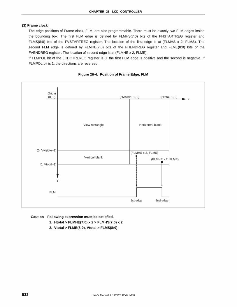
CHAPTER 26 LCD CONTROLLER
User’s Manual U14272EJ1V0UM00532
(3) Frame clock
The edge positions of Frame clock, FLM, are also programmable. There must be exactly two FLM edges inside
the bounding box. The first FLM edge is defined by FLMHS(7:0) bits of the FHSTARTREG register and
FLMS(8:0) bits of the FVSTARTREG register. The location of the first edge is at (FLMHS x 2, FLMS). The
second FLM edge is defined by FLMHE(7:0) bits of the FHENDREG register and FLME(8:0) bits of the
FVENDREG register. The location of second edge is at (FLMHE x 2, FLME).
If FLMPOL bit of the LCDCTRLREG register is 0, the first FLM edge is positive and the second is negative. If
FLMPOL bit is 1, the directions are reversed.
Figure 26-4. Position of Frame Edge, FLM
Origin(0, 0) (Hvisible−1, 0) (Htotal−1, 0)
View rectangle
FLM
(0, Vvisible−1)
Vertical blank
Y
X
Horizontal blank
(0, Vtotal−1)
(FLMHS x 2, FLMS)
1st edge 2nd edge
(FLMHE x 2, FLME)
Caution Following expression must be satisfied.
1. Htotal > FLMHE(7:0) x 2 > FLMHS(7:0) x 2
2. Vtotal > FLME(8:0), Vtotal > FLMS(8:0)
CHAPTER 26 LCD CONTROLLER
User’s Manual U14272EJ1V0UM00 533
(4) Shift clock
Shift clock (SHCLK) edges can be programmed only indirectly. Shift clocks occur in rows of the vertical blank
rectangle only if DummyL bit of the VRVISIBREG register is 1. The position of SHCLK edges are controlled by
Panelcolor and PanDBus bits of the LCDCFGREG0 register. The SCLKPOL bit of the LCDCTRLREG register
determines whether data is latched into the panel on the rising or falling edges. If SCLKPOL bit is 0, data is
latched on the falling edges.
(5) M signal
Some panels also need a modulation signal, M, to operate properly. The modulation rate is controlled by
MOD(7:0) bits of the LCDCFGREG0 register. If Mod field is 0, M toggles once per frame. If Mod field is not 0,
then M toggles once every rows whose number is set in Mod field. M toggles at LCE position, the same time as
the second LOCLK edge. When Mod field is 0, M toggles when LOCLK latches FLM.
(6) Vertical retrace interrupt
When the controller goes through the vertical blank rectangle, a status signal bit VIReq of the LCDINRQREG
register becomes 1. This signal can be polled, or configured to generate an interrupt. To enable the interrupt, set
MVIReq bit of LCDIMSKREG register to 1. Once the interrupt is generated, writing to VIReq bit clears the
interrupt. However, the state of VIReq bit changes to 0 only after the controller returns to top left corner. Note that
there is some delay between the controller’s entering or leaving the vertical blank rectangle and the changes in
VIReq bit.
26.3.2 Controller clocks
All LCD controller timing is based on the internal clock hpck. The hpck is derived from gclk, which is derived from
the MBA clock (TClock). The frequency of gclk can be equal to, one-half of, or one-quarter of that of the MBA clock,
depending on Pre-scal(1:0) bits of the LCDCFGREG0 register and the MBA clock frequency. The hpck frequency is
programmable. In each cycle hpck is high for cycles set in HpckH(5:0) bits of the LCDCFGREG1 register, and low for
cycles set in HpckL(5:0) bits of the LCDCFGREG1 register. The values in HpckH and HpckL fields are not arbitrary.
Their sum must be at least 5, and the following condition must be satisfied:
fhpck ≈ Htotal x Vtotal x frefresh
Both hpck and gclk can be turned off when the panel is inactive. Setting ContCkE bit of the LCDCTRLREG
register to 1 initializes the controller and turns on both clocks, or 0 turns them off.
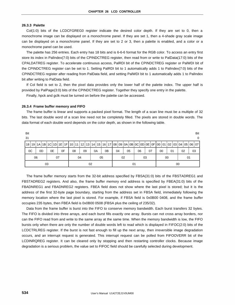
CHAPTER 26 LCD CONTROLLER
User’s Manual U14272EJ1V0UM00534
26.3.3 Palette
Col(1:0) bits of the LCDCFGREG0 register indicate the desired color depth. If they are set to 0, then a
monochrome image can be displayed on a monochrome panel. If they are set 1, then a 4-shade gray scale image
can be displayed on a monochrome panel. If they are set to 2 or 3, then a palette is enabled, and a color or a
monochrome panel can be used.
The palette has 256 entries. Each entry has 18 bits and is 6-6-6 format for the RGB color. To access an entry first
store its index in PalIndex(7:0) bits of the CPINDCTREG register, then read from or write to PalData(17:0) bits of the
CPALDATREG register. To accelerate continuous access, PalRDI bit of the CPINDCTREG register or PalWDI bit of
the CPINDCTREG register can be set to 1. Setting PalRDI bit to 1 automatically adds 1 to PalIndex(7:0) bits of the
CPINDCTREG register after reading from PalData field, and setting PalWDI bit to 1 automatically adds 1 to PalIndex
bit after writing to PalData field.
If Col field is set to 2, then the pixel data provides only the lower half of the palette index. The upper half is
provided by PalPage(3:0) bits of the CPINDCTREG register. Together they specify one entry in the palette.
Finally, hpck and gclk must be turned on before the palette can be accessed.
26.3.4 Frame buffer memory and FIFO
The frame buffer is linear and supports a packed pixel format. The length of a scan line must be a multiple of 32
bits. The last double word of a scan line need not be completely filled. The pixels are stored in double words. The
data format of each double word depends on the color depth, as shown in the following table.
Bit
31
Bit
0
18 19 1A 1B 1C 1D 1E 1F 10 11 12 13 14 15 16 17 08 09 0A 0B 0C 0D 0E 0F 00 01 02 03 04 05 06 07
0C 0D 0E 0F 08 09 0A 0B 04 05 06 07 00 01 02 03
06 07 04 05 02 03 00 01
03 02 01 00
The frame buffer memory starts from the 32-bit address specified by FBSA(31:0) bits of the FBSTADREG1 and
FBSTADREG2 registers. And also, the frame buffer memory end address is specified by FBEA(31:0) bits of the
FBADNREG1 and FBADNREG2 registers. FBEA field does not show where the last pixel is stored; but it is the
address of the first 32-byte page boundary, starting from the address set in FBSA field, immediately following the
memory location where the last pixel is stored. For example, if FBSA field is 0x0B00 0408, and the frame buffer
occupies 235 bytes, then FBEA field is 0x0B00 0508 (FBSA plus the ceiling of 235/32).
Data from the frame buffer is burst into the FIFO to conserve memory bandwidth. Each burst transfers 32 bytes.
The FIFO is divided into three arrays, and each burst fills exactly one array. Bursts can not cross array borders, nor
can the FIFO read from and write to the same array at the same time. When the memory bandwidth is low, the FIFO
bursts only when there are only the number of double words left to read which is displayed in FIFOC(2:0) bits of the
LCDCTRLREG register. If the burst is not fast enough to fill up the next array, then irreversible image degradation
occurs, and an interrupt request is generated. This interrupt request can be polled from FIFOOVERR bit of the
LCDINRQREG register. It can be cleared only by stopping and then restarting controller clocks. Because image
degradation is a serious problem, the value set to FIFOC field should be carefully selected during development.
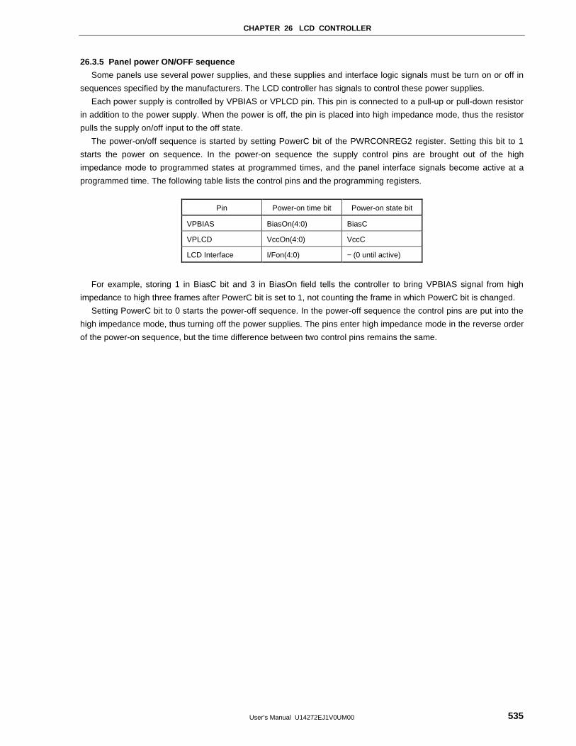
CHAPTER 26 LCD CONTROLLER
User’s Manual U14272EJ1V0UM00 535
26.3.5 Panel power ON/OFF sequence
Some panels use several power supplies, and these supplies and interface logic signals must be turn on or off in
sequences specified by the manufacturers. The LCD controller has signals to control these power supplies.
Each power supply is controlled by VPBIAS or VPLCD pin. This pin is connected to a pull-up or pull-down resistor
in addition to the power supply. When the power is off, the pin is placed into high impedance mode, thus the resistor
pulls the supply on/off input to the off state.
The power-on/off sequence is started by setting PowerC bit of the PWRCONREG2 register. Setting this bit to 1
starts the power on sequence. In the power-on sequence the supply control pins are brought out of the high
impedance mode to programmed states at programmed times, and the panel interface signals become active at a
programmed time. The following table lists the control pins and the programming registers.
Pin Power-on time bit Power-on state bit
VPBIAS BiasOn(4:0) BiasC
VPLCD VccOn(4:0) VccC
LCD Interface I/Fon(4:0) − (0 until active)
For example, storing 1 in BiasC bit and 3 in BiasOn field tells the controller to bring VPBIAS signal from high
impedance to high three frames after PowerC bit is set to 1, not counting the frame in which PowerC bit is changed.
Setting PowerC bit to 0 starts the power-off sequence. In the power-off sequence the control pins are put into the
high impedance mode, thus turning off the power supplies. The pins enter high impedance mode in the reverse order
of the power-on sequence, but the time difference between two control pins remains the same.
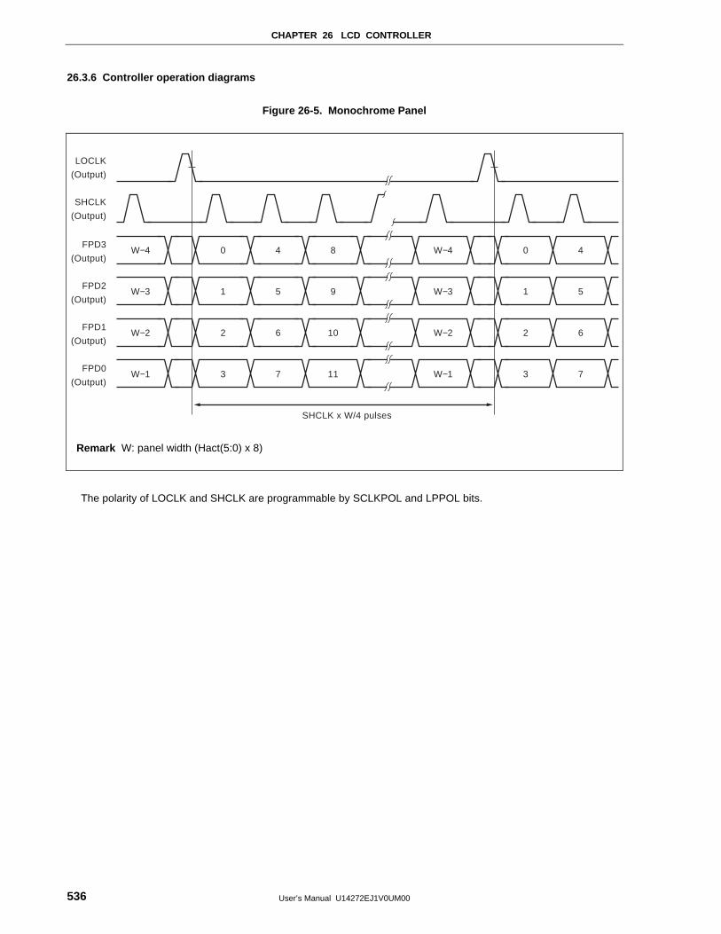
CHAPTER 26 LCD CONTROLLER
User’s Manual U14272EJ1V0UM00536
26.3.6 Controller operation diagrams
Figure 26-5. Monochrome Panel
FPD2
(Output)
FPD3
(Output)W−4 0 4 8
FPD0
(Output)
FPD1
(Output)W−2 2 6 10
SHCLK
(Output)
LOCLK
(Output)
W−3 1 5 9
W−1 3 7 11
W−4 0 4
W−2 2 6
W−3 1 5
W−1 3 7
SHCLK x W/4 pulses
Remark W: panel width (Hact(5:0) x 8)
The polarity of LOCLK and SHCLK are programmable by SCLKPOL and LPPOL bits.
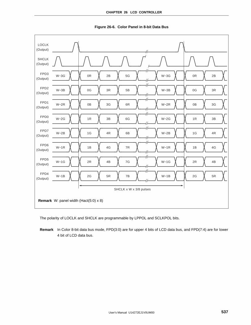
CHAPTER 26 LCD CONTROLLER
User’s Manual U14272EJ1V0UM00 537
Figure 26-6. Color Panel in 8-bit Data Bus
FPD2
(Output)
FPD3
(Output)W−3G 0R 2B 5G
FPD0
(Output)
FPD1
(Output)W−2R 0B 3G 6R
SHCLK
(Output)
LOCLK
(Output)
W−3B 0G 3R 5B
W−2G 1R 3B 6G
SHCLK x W x 3/8 pulses
FPD6
(Output)
FPD7
(Output)W−2B 1G 4R 6B
FPD4
(Output)
FPD5
(Output)W−1G 2R 4B 7G
W−1R 1B 4G 7R
W−1B 2G 5R 7B
W−3G 0R 2B
W−2R 0B 3G
W−3B 0G 3R
W−2G 1R 3B
W−2B 1G 4R
W−1G 2R 4B
W−1R 1B 4G
W−1B 2G 5R
Remark W: panel width (Hact(5:0) x 8)
The polarity of LOCLK and SHCLK are programmable by LPPOL and SCLKPOL bits.
Remark In Color 8-bit data bus mode, FPD(3:0) are for upper 4 bits of LCD data bus, and FPD(7:4) are for lower
4 bit of LCD data bus.
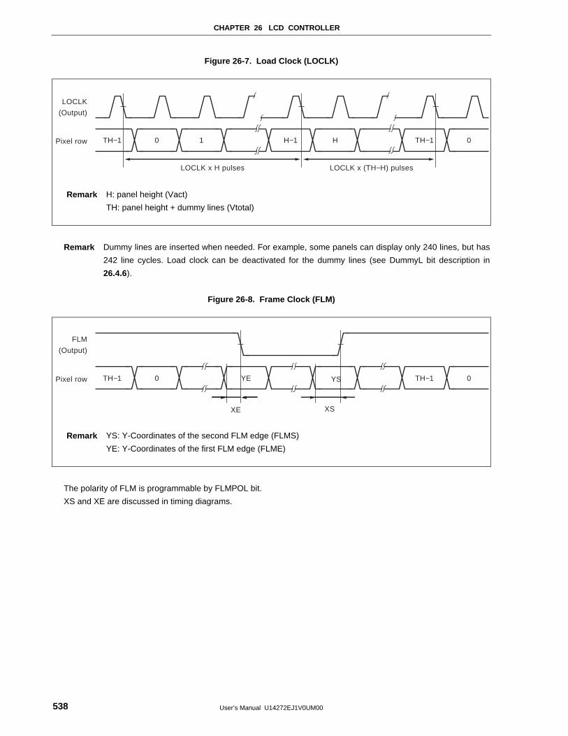
CHAPTER 26 LCD CONTROLLER
User’s Manual U14272EJ1V0UM00538
Figure 26-7. Load Clock (LOCLK)
Pixel row 0 1
LOCLK
(Output)
H−1 H 0
LOCLK x H pulses LOCLK x (TH−H) pulses
TH−1 TH−1
Remark H: panel height (Vact)
TH: panel height + dummy lines (Vtotal)
Remark Dummy lines are inserted when needed. For example, some panels can display only 240 lines, but has
242 line cycles. Load clock can be deactivated for the dummy lines (see DummyL bit description in
26.4.6).
Figure 26-8. Frame Clock (FLM)
Pixel row 0 YE
FLM
(Output)
YS 0
XE XS
TH−1 TH−1
Remark YS: Y-Coordinates of the second FLM edge (FLMS)
YE: Y-Coordinates of the first FLM edge (FLME)
The polarity of FLM is programmable by FLMPOL bit.
XS and XE are discussed in timing diagrams.
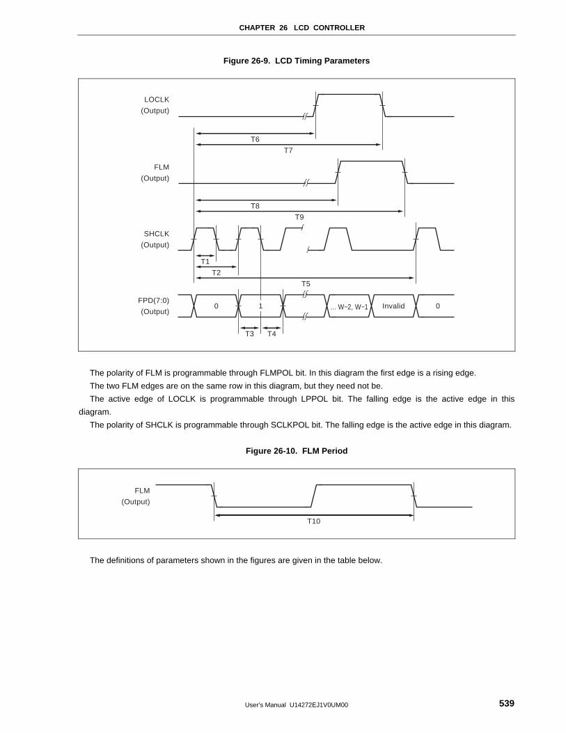
CHAPTER 26 LCD CONTROLLER
User’s Manual U14272EJ1V0UM00 539
Figure 26-9. LCD Timing Parameters
FLM
(Output)
FPD(7:0)
(Output)
SHCLK
(Output)
LOCLK
(Output)
T6
T7
... W−2, W−1
T5
T8
T9
T1
T2
T3 T4
0 Invalid1 0
The polarity of FLM is programmable through FLMPOL bit. In this diagram the first edge is a rising edge.
The two FLM edges are on the same row in this diagram, but they need not be.
The active edge of LOCLK is programmable through LPPOL bit. The falling edge is the active edge in this
diagram.
The polarity of SHCLK is programmable through SCLKPOL bit. The falling edge is the active edge in this diagram.
Figure 26-10. FLM Period
FLM
(Output)
T10
The definitions of parameters shown in the figures are given in the table below.
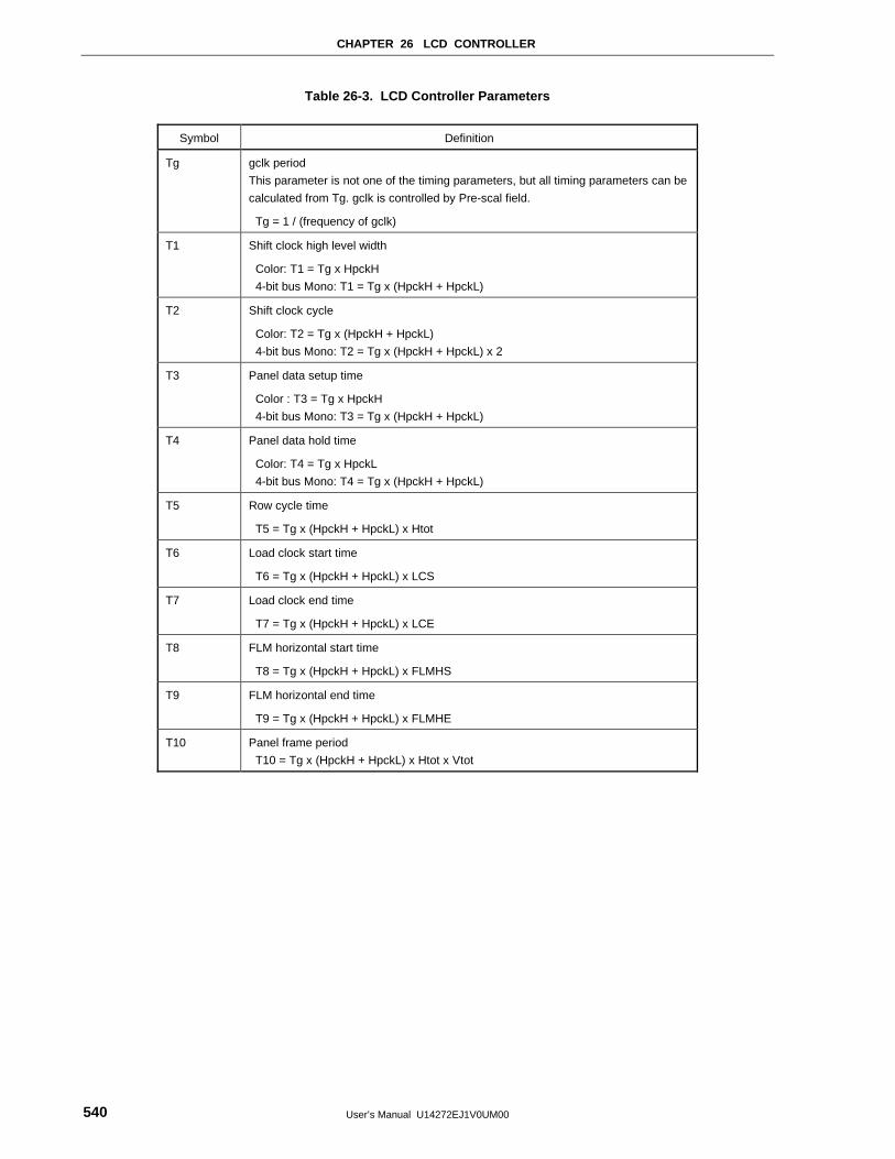
CHAPTER 26 LCD CONTROLLER
User’s Manual U14272EJ1V0UM00540
Table 26-3. LCD Controller Parameters
Symbol Definition
Tg gclk period
This parameter is not one of the timing parameters, but all timing parameters can be
calculated from Tg. gclk is controlled by Pre-scal field.
Tg = 1 / (frequency of gclk)
T1 Shift clock high level width
Color: T1 = Tg x HpckH
4-bit bus Mono: T1 = Tg x (HpckH + HpckL)
T2 Shift clock cycle
Color: T2 = Tg x (HpckH + HpckL)
4-bit bus Mono: T2 = Tg x (HpckH + HpckL) x 2
T3 Panel data setup time
Color : T3 = Tg x HpckH
4-bit bus Mono: T3 = Tg x (HpckH + HpckL)
T4 Panel data hold time
Color: T4 = Tg x HpckL
4-bit bus Mono: T4 = Tg x (HpckH + HpckL)
T5 Row cycle time
T5 = Tg x (HpckH + HpckL) x Htot
T6 Load clock start time
T6 = Tg x (HpckH + HpckL) x LCS
T7 Load clock end time
T7 = Tg x (HpckH + HpckL) x LCE
T8 FLM horizontal start time
T8 = Tg x (HpckH + HpckL) x FLMHS
T9 FLM horizontal end time
T9 = Tg x (HpckH + HpckL) x FLMHE
T10 Panel frame period
T10 = Tg x (HpckH + HpckL) x Htot x Vtot
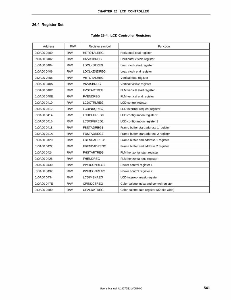
CHAPTER 26 LCD CONTROLLER
User’s Manual U14272EJ1V0UM00 541
26.4 Register Set
Table 26-4. LCD Controller Registers
Address R/W Register symbol Function
0x0A00 0400 R/W HRTOTALREG Horizontal total register
0x0A00 0402 R/W HRVISIBREG Horizontal visible register
0x0A00 0404 R/W LDCLKSTREG Load clock start register
0x0A00 0406 R/W LDCLKENDREG Load clock end register
0x0A00 0408 R/W VRTOTALREG Vertical total register
0x0A00 040A R/W VRVISBREG Vertical visible register
0x0A00 040C R/W FVSTARTREG FLM vertical start register
0x0A00 040E R/W FVENDREG FLM vertical end register
0x0A00 0410 R/W LCDCTRLREG LCD control register
0x0A00 0412 R/W LCDINRQREG LCD interrupt request register
0x0A00 0414 R/W LCDCFGREG0 LCD configuration register 0
0x0A00 0416 R/W LCDCFGREG1 LCD configuration register 1
0x0A00 0418 R/W FBSTADREG1 Frame buffer start address 1 register
0x0A00 041A R/W FBSTADREG2 Frame buffer start address 2 register
0x0A00 0420 R/W FBENDADREG1 Frame buffer end address 1 register
0x0A00 0422 R/W FBENDADREG2 Frame buffer end address 2 register
0x0A00 0424 R/W FHSTARTREG FLM horizontal start register
0x0A00 0426 R/W FHENDREG FLM horizontal end register
0x0A00 0430 R/W PWRCONREG1 Power control register 1
0x0A00 0432 R/W PWRCONREG2 Power control register 2
0x0A00 0434 R/W LCDIMSKREG LCD interrupt mask register
0x0A00 047E R/W CPINDCTREG Color palette index and control register
0x0A00 0480 R/W CPALDATREG Color palette data register (32 bits wide)
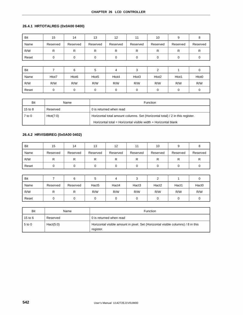
CHAPTER 26 LCD CONTROLLER
User’s Manual U14272EJ1V0UM00542
26.4.1 HRTOTALREG (0x0A00 0400)
Bit 15 14 13 12 11 10 9 8
Name Reserved Reserved Reserved Reserved Reserved Reserved Reserved Reserved
R/W R R R R R R R R
Reset 0 0 0 0 0 0 0 0
Bit 7 6 5 4 3 2 1 0
Name Htot7 Htot6 Htot5 Htot4 Htot3 Htot2 Htot1 Htot0
R/W R/W R/W R/W R/W R/W R/W R/W R/W
Reset 0 0 0 0 0 0 0 0
Bit Name Function
15 to 8 Reserved 0 is returned when read
7 to 0 Htot(7:0) Horizontal total amount columns. Set (Horizontal total) / 2 in this register.
Horizontal total = Horizontal visible width + Horizontal blank
26.4.2 HRVISIBREG (0x0A00 0402)
Bit 15 14 13 12 11 10 9 8
Name Reserved Reserved Reserved Reserved Reserved Reserved Reserved Reserved
R/W R R R R R R R R
Reset 0 0 0 0 0 0 0 0
Bit 7 6 5 4 3 2 1 0
Name Reserved Reserved Hact5 Hact4 Hact3 Hact2 Hact1 Hact0
R/W R R R/W R/W R/W R/W R/W R/W
Reset 0 0 0 0 0 0 0 0
Bit Name Function
15 to 6 Reserved 0 is returned when read
5 to 0 Hact(5:0) Horizontal visible amount in pixel. Set (Horizontal visible columns) / 8 in this
register.
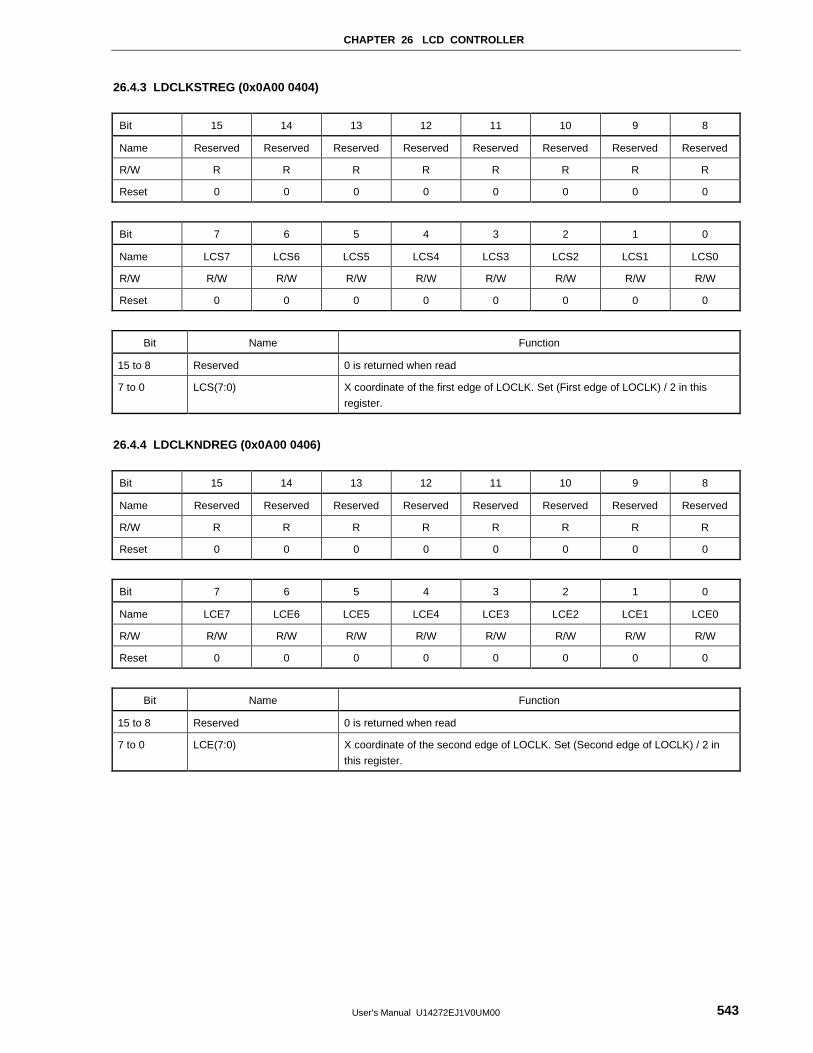
CHAPTER 26 LCD CONTROLLER
User’s Manual U14272EJ1V0UM00 543
26.4.3 LDCLKSTREG (0x0A00 0404)
Bit 15 14 13 12 11 10 9 8
Name Reserved Reserved Reserved Reserved Reserved Reserved Reserved Reserved
R/W R R R R R R R R
Reset 0 0 0 0 0 0 0 0
Bit 7 6 5 4 3 2 1 0
Name LCS7 LCS6 LCS5 LCS4 LCS3 LCS2 LCS1 LCS0
R/W R/W R/W R/W R/W R/W R/W R/W R/W
Reset 0 0 0 0 0 0 0 0
Bit Name Function
15 to 8 Reserved 0 is returned when read
7 to 0 LCS(7:0) X coordinate of the first edge of LOCLK. Set (First edge of LOCLK) / 2 in this
register.
26.4.4 LDCLKNDREG (0x0A00 0406)
Bit 15 14 13 12 11 10 9 8
Name Reserved Reserved Reserved Reserved Reserved Reserved Reserved Reserved
R/W R R R R R R R R
Reset 0 0 0 0 0 0 0 0
Bit 7 6 5 4 3 2 1 0
Name LCE7 LCE6 LCE5 LCE4 LCE3 LCE2 LCE1 LCE0
R/W R/W R/W R/W R/W R/W R/W R/W R/W
Reset 0 0 0 0 0 0 0 0
Bit Name Function
15 to 8 Reserved 0 is returned when read
7 to 0 LCE(7:0) X coordinate of the second edge of LOCLK. Set (Second edge of LOCLK) / 2 in
this register.
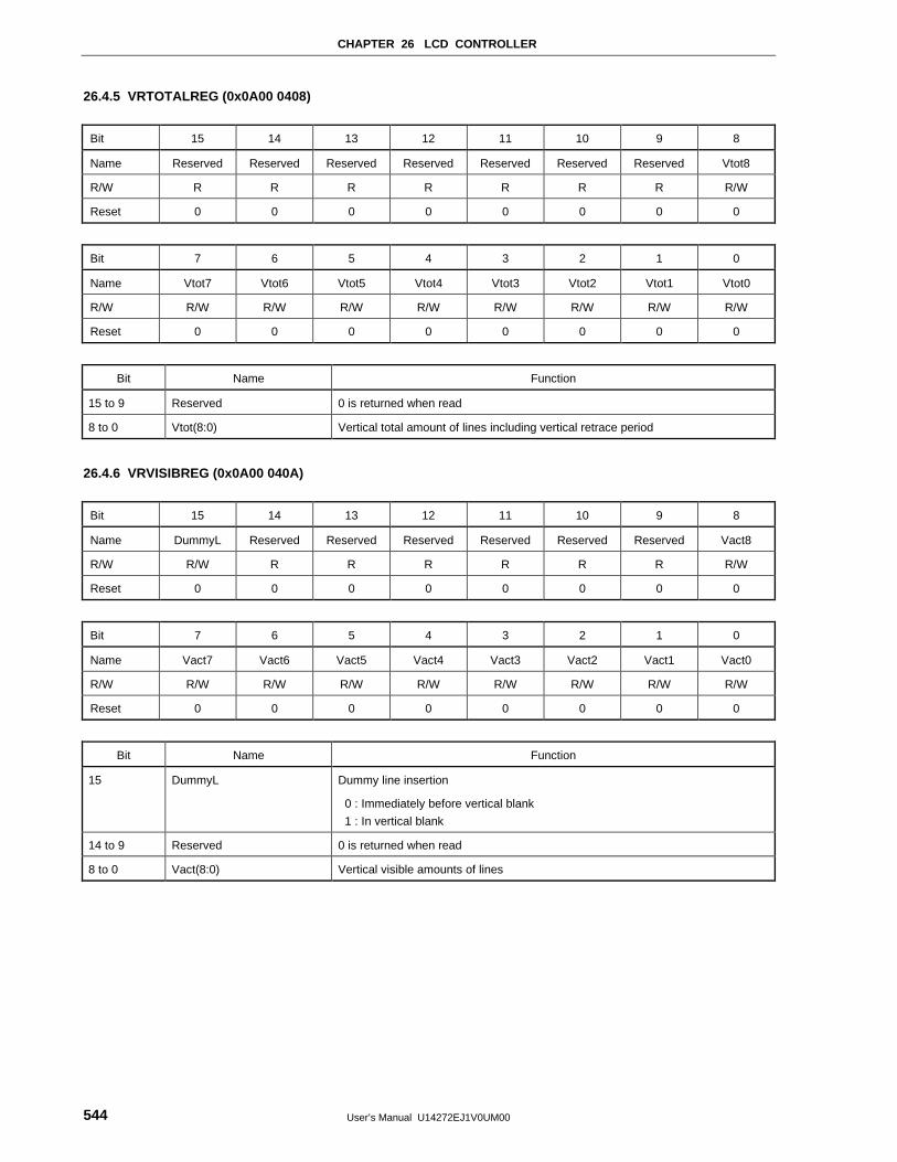
CHAPTER 26 LCD CONTROLLER
User’s Manual U14272EJ1V0UM00544
26.4.5 VRTOTALREG (0x0A00 0408)
Bit 15 14 13 12 11 10 9 8
Name Reserved Reserved Reserved Reserved Reserved Reserved Reserved Vtot8
R/W R R R R R R R R/W
Reset 0 0 0 0 0 0 0 0
Bit 7 6 5 4 3 2 1 0
Name Vtot7 Vtot6 Vtot5 Vtot4 Vtot3 Vtot2 Vtot1 Vtot0
R/W R/W R/W R/W R/W R/W R/W R/W R/W
Reset 0 0 0 0 0 0 0 0
Bit Name Function
15 to 9 Reserved 0 is returned when read
8 to 0 Vtot(8:0) Vertical total amount of lines including vertical retrace period
26.4.6 VRVISIBREG (0x0A00 040A)
Bit 15 14 13 12 11 10 9 8
Name DummyL Reserved Reserved Reserved Reserved Reserved Reserved Vact8
R/W R/W R R R R R R R/W
Reset 0 0 0 0 0 0 0 0
Bit 7 6 5 4 3 2 1 0
Name Vact7 Vact6 Vact5 Vact4 Vact3 Vact2 Vact1 Vact0
R/W R/W R/W R/W R/W R/W R/W R/W R/W
Reset 0 0 0 0 0 0 0 0
Bit Name Function
15 DummyL Dummy line insertion
0 : Immediately before vertical blank
1 : In vertical blank
14 to 9 Reserved 0 is returned when read
8 to 0 Vact(8:0) Vertical visible amounts of lines
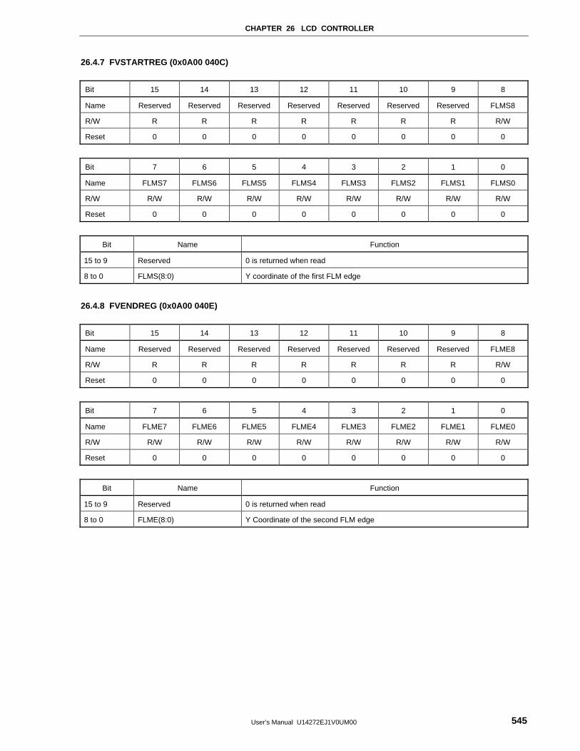
CHAPTER 26 LCD CONTROLLER
User’s Manual U14272EJ1V0UM00 545
26.4.7 FVSTARTREG (0x0A00 040C)
Bit 15 14 13 12 11 10 9 8
Name Reserved Reserved Reserved Reserved Reserved Reserved Reserved FLMS8
R/W R R R R R R R R/W
Reset 0 0 0 0 0 0 0 0
Bit 7 6 5 4 3 2 1 0
Name FLMS7 FLMS6 FLMS5 FLMS4 FLMS3 FLMS2 FLMS1 FLMS0
R/W R/W R/W R/W R/W R/W R/W R/W R/W
Reset 0 0 0 0 0 0 0 0
Bit Name Function
15 to 9 Reserved 0 is returned when read
8 to 0 FLMS(8:0) Y coordinate of the first FLM edge
26.4.8 FVENDREG (0x0A00 040E)
Bit 15 14 13 12 11 10 9 8
Name Reserved Reserved Reserved Reserved Reserved Reserved Reserved FLME8
R/W R R R R R R R R/W
Reset 0 0 0 0 0 0 0 0
Bit 7 6 5 4 3 2 1 0
Name FLME7 FLME6 FLME5 FLME4 FLME3 FLME2 FLME1 FLME0
R/W R/W R/W R/W R/W R/W R/W R/W R/W
Reset 0 0 0 0 0 0 0 0
Bit Name Function
15 to 9 Reserved 0 is returned when read
8 to 0 FLME(8:0) Y Coordinate of the second FLM edge
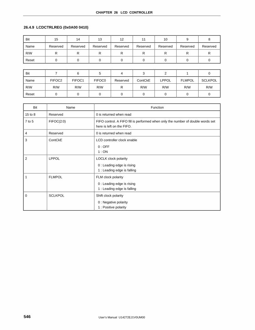
CHAPTER 26 LCD CONTROLLER
User’s Manual U14272EJ1V0UM00546
26.4.9 LCDCTRLREG (0x0A00 0410)
Bit 15 14 13 12 11 10 9 8
Name Reserved Reserved Reserved Reserved Reserved Reserved Reserved Reserved
R/W R R R R R R R R
Reset 0 0 0 0 0 0 0 0
Bit 7 6 5 4 3 2 1 0
Name FIFOC2 FIFOC1 FIFOC0 Reserved ContCkE LPPOL FLMPOL SCLKPOL
R/W R/W R/W R/W R R/W R/W R/W R/W
Reset 0 0 0 0 0 0 0 0
Bit Name Function
15 to 8 Reserved 0 is returned when read
7 to 5 FIFOC(2:0) FIFO control. A FIFO fill is performed when only the number of double words set
here is left on the FIFO.
4 Reserved 0 is returned when read
3 ContCkE LCD controller clock enable
0 : OFF
1 : ON
2 LPPOL LOCLK clock polarity
0 : Leading edge is rising
1 : Leading edge is falling
1 FLMPOL FLM clock polarity
0 : Leading edge is rising
1 : Leading edge is falling
0 SCLKPOL Shift clock polarity
0 : Negative polarity
1 : Positive polarity
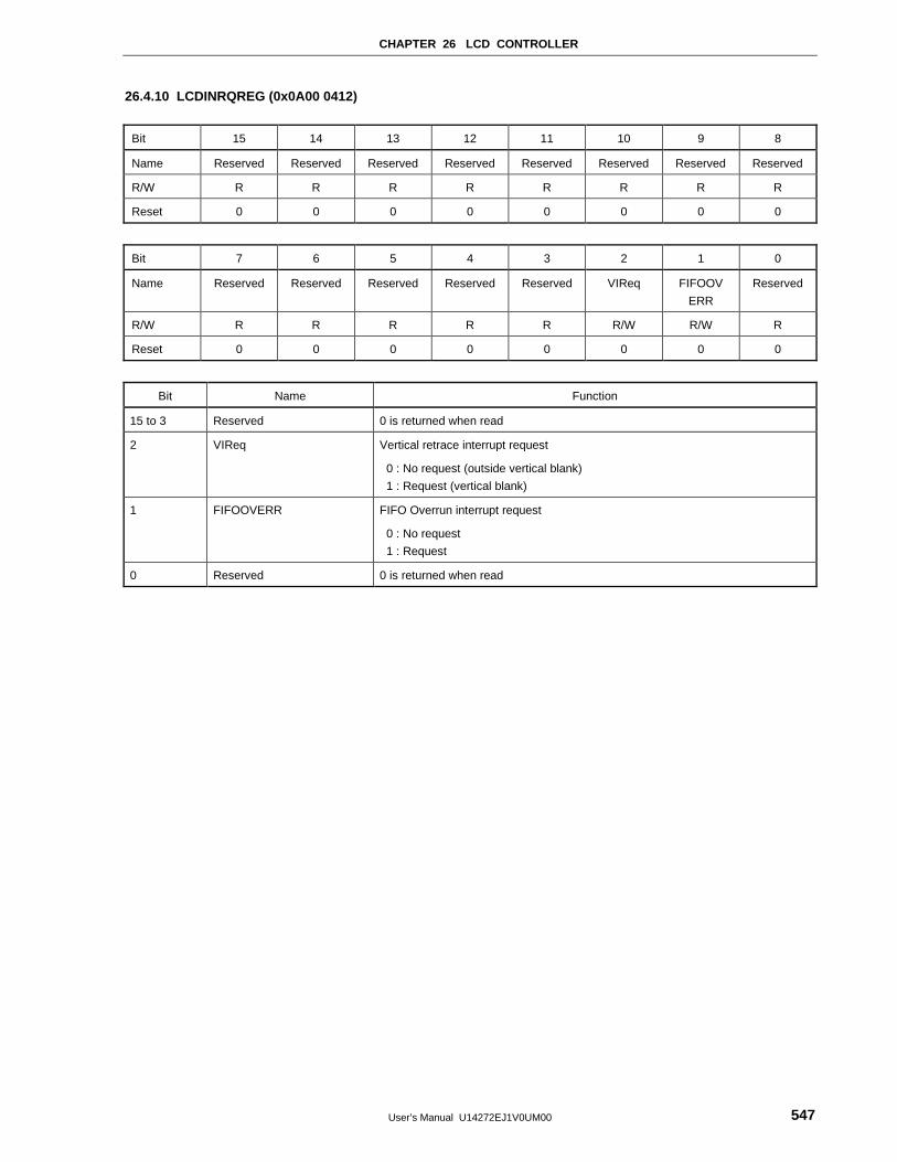
CHAPTER 26 LCD CONTROLLER
User’s Manual U14272EJ1V0UM00 547
26.4.10 LCDINRQREG (0x0A00 0412)
Bit 15 14 13 12 11 10 9 8
Name Reserved Reserved Reserved Reserved Reserved Reserved Reserved Reserved
R/W R R R R R R R R
Reset 0 0 0 0 0 0 0 0
Bit 7 6 5 4 3 2 1 0
Name Reserved Reserved Reserved Reserved Reserved VIReq FIFOOV
ERR
Reserved
R/W R R R R R R/W R/W R
Reset 0 0 0 0 0 0 0 0
Bit Name Function
15 to 3 Reserved 0 is returned when read
2 VIReq Vertical retrace interrupt request
0 : No request (outside vertical blank)
1 : Request (vertical blank)
1 FIFOOVERR FIFO Overrun interrupt request
0 : No request
1 : Request
0 Reserved 0 is returned when read
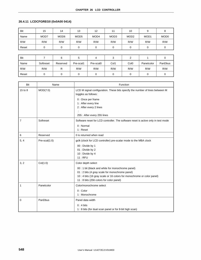
CHAPTER 26 LCD CONTROLLER
User’s Manual U14272EJ1V0UM00548
26.4.11 LCDCFGREG0 (0x0A00 0414)
Bit 15 14 13 12 11 10 9 8
Name MOD7 MOD6 MOD5 MOD4 MOD3 MOD2 MOD1 MOD0
R/W R/W R/W R/W R/W R/W R/W R/W R/W
Reset 0 0 0 0 0 0 0 0
Bit 7 6 5 4 3 2 1 0
Name Softreset Reserved Pre-scal1 Pre-scal0 Col1 Col0 Panelcolor PanDbus
R/W R/W R R/W R/W R/W R/W R/W R/W
Reset 0 0 0 0 0 0 0 0
Bit Name Function
15 to 8 MOD(7:0) LCD M signal configuration. These bits specify the number of lines between M
toggles as follows:
0 : Once per frame
1 : After every line
2 : After every 2 lines
:
255 : After every 255 lines
7 Softreset Software reset for LCD controller. The software reset is active only in test mode
0 : Normal
1 : Reset
6 Reserved 0 is returned when read
5, 4 Pre-scal(1:0) gclk (clock for LCD controller) pre-scalar mode to the MBA clock
00 : Divide by 1
01 : Divide by 2
10 : Divide by 4
11 : RFU
3, 2 Col(1:0) Color depth select
00 : 1 bit (black and white for monochrome panel)
01 : 2 bits (4 gray scale for monochrome panel)
10 : 4 bits (16 gray scale or 16 colors for monochrome or color panel)
11 : 8 bits (256 colors for color panel)
1 Panelcolor Color/monochrome select
0 : Color
1 : Monochrome
0 PanDbus Panel data width
0 : 4 bits
1 : 8 bits (for dual scan panel or for 8-bit high scan)

CHAPTER 26 LCD CONTROLLER
User’s Manual U14272EJ1V0UM00 549
26.4.12 LCDCFGREG1 (0x0A00 0416)
Bit 15 14 13 12 11 10 9 8
Name Reserved Reserved HpckL5 HpckL4 HpckL3 HpckL2 HpckL1 HpckL0
R/W R R R/W R/W R/W R/W R/W R/W
Reset 0 0 0 0 0 0 0 0
Bit 7 6 5 4 3 2 1 0
Name Reserved Reserved HpckH5 HpckH4 HpckH3 HpckH2 HpckH1 HpckH0
R/W R R R/W R/W R/W R/W R/W R/W
Reset 0 0 0 0 0 0 0 0
Bit Name Function
15, 14 Reserved 0 is returned when read
13 to 8 HpckL(5:0) Number of gclk cycles for Hpck low time
7, 6 Reserved 0 is returned when read
5 to 0 HpckH(5:0) Number of gclk cycles for Hpck high time
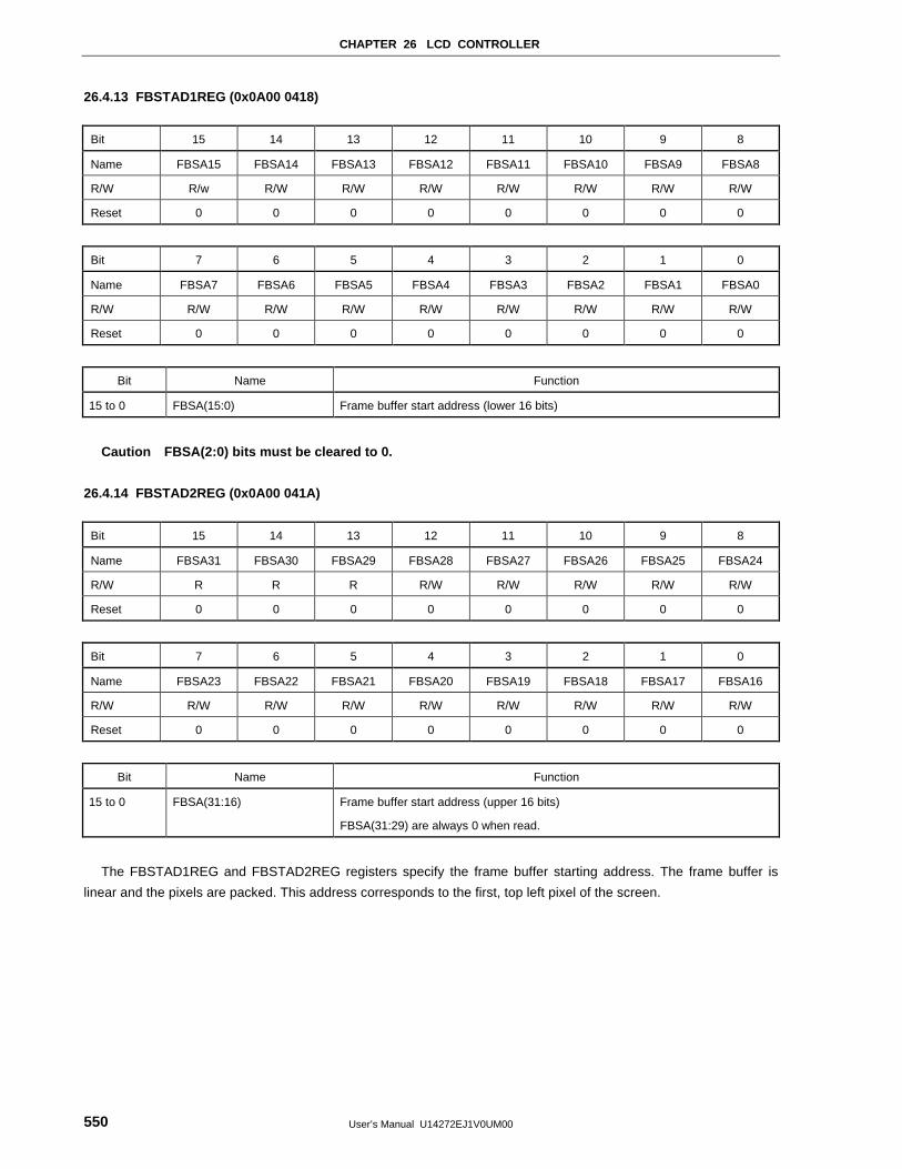
CHAPTER 26 LCD CONTROLLER
User’s Manual U14272EJ1V0UM00550
26.4.13 FBSTAD1REG (0x0A00 0418)
Bit 15 14 13 12 11 10 9 8
Name FBSA15 FBSA14 FBSA13 FBSA12 FBSA11 FBSA10 FBSA9 FBSA8
R/W R/w R/W R/W R/W R/W R/W R/W R/W
Reset 0 0 0 0 0 0 0 0
Bit 7 6 5 4 3 2 1 0
Name FBSA7 FBSA6 FBSA5 FBSA4 FBSA3 FBSA2 FBSA1 FBSA0
R/W R/W R/W R/W R/W R/W R/W R/W R/W
Reset 0 0 0 0 0 0 0 0
Bit Name Function
15 to 0 FBSA(15:0) Frame buffer start address (lower 16 bits)
Caution FBSA(2:0) bits must be cleared to 0.
26.4.14 FBSTAD2REG (0x0A00 041A)
Bit 15 14 13 12 11 10 9 8
Name FBSA31 FBSA30 FBSA29 FBSA28 FBSA27 FBSA26 FBSA25 FBSA24
R/W R R R R/W R/W R/W R/W R/W
Reset 0 0 0 0 0 0 0 0
Bit 7 6 5 4 3 2 1 0
Name FBSA23 FBSA22 FBSA21 FBSA20 FBSA19 FBSA18 FBSA17 FBSA16
R/W R/W R/W R/W R/W R/W R/W R/W R/W
Reset 0 0 0 0 0 0 0 0
Bit Name Function
15 to 0 FBSA(31:16) Frame buffer start address (upper 16 bits)
FBSA(31:29) are always 0 when read.
The FBSTAD1REG and FBSTAD2REG registers specify the frame buffer starting address. The frame buffer is
linear and the pixels are packed. This address corresponds to the first, top left pixel of the screen.
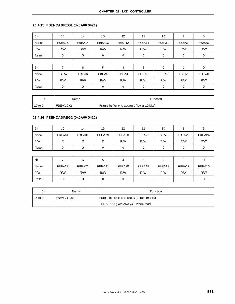
CHAPTER 26 LCD CONTROLLER
User’s Manual U14272EJ1V0UM00 551
26.4.15 FBENDADREG1 (0x0A00 0420)
Bit 15 14 13 12 11 10 9 8
Name FBEA15 FBEA14 FBEA13 FBEA12 FBEA11 FBEA10 FBEA9 FBEA8
R/W R/W R/W R/W R/W R/W R/W R/W R/W
Reset 0 0 0 0 0 0 0 0
Bit 7 6 5 4 3 2 1 0
Name FBEA7 FBEA6 FBEA5 FBEA4 FBEA3 FBEA2 FBEA1 FBEA0
R/W R/W R/W R/W R/W R/W R/W R/W R/W
Reset 0 0 0 0 0 0 0 0
Bit Name Function
15 to 0 FBEA(15:0) Frame buffer end address (lower 16 bits)
26.4.16 FBENDADREG2 (0x0A00 0422)
Bit 15 14 13 12 11 10 9 8
Name FBEA31 FBEA30 FBEA29 FBEA28 FBEA27 FBEA26 FBEA25 FBEA24
R/W R R R R/W R/W R/W R/W R/W
Reset 0 0 0 0 0 0 0 0
bit 7 6 5 4 3 2 1 0
Name FBEA23 FBEA22 FBEA21 FBEA20 FBEA19 FBEA18 FBEA17 FBEA16
R/W R/W R/W R/W R/W R/W R/W R/W R/W
Reset 0 0 0 0 0 0 0 0
Bit Name Function
15 to 0 FBEA(31:16) Frame buffer end address (upper 16 bits)
FBEA(31:29) are always 0 when read.
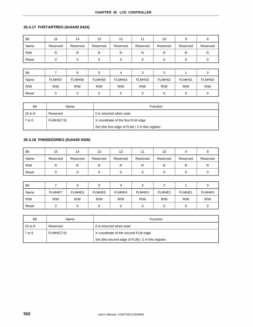
CHAPTER 26 LCD CONTROLLER
User’s Manual U14272EJ1V0UM00552
26.4.17 FHSTARTREG (0x0A00 0424)
Bit 15 14 13 12 11 10 9 8
Name Reserved Reserved Reserved Reserved Reserved Reserved Reserved Reserved
R/W R R R R R R R R
Reset 0 0 0 0 0 0 0 0
Bit 7 6 5 4 3 2 1 0
Name FLMHS7 FLMHS6 FLMHS5 FLMHS4 FLMHS3 FLMHS2 FLMHS1 FLMHS0
R/W R/W R/W R/W R/W R/W R/W R/W R/W
Reset 0 0 0 0 0 0 0 0
Bit Name Function
15 to 8 Reserved 0 is returned when read
7 to 0 FLMHS(7:0) X coordinate of the first FLM edge
Set (the first edge of FLM) / 2 in this register.
26.4.18 FHNSEDGREG (0x0A00 0426)
Bit 15 14 13 12 11 10 9 8
Name Reserved Reserved Reserved Reserved Reserved Reserved Reserved Reserved
R/W R R R R R R R R
Reset 0 0 0 0 0 0 0 0
Bit 7 6 5 4 3 2 1 0
Name FLMHE7 FLMHE6 FLMHE5 FLMHE4 FLMHE3 FLMHE2 FLMHE1 FLMHE0
R/W R/W R/W R/W R/W R/W R/W R/W R/W
Reset 0 0 0 0 0 0 0 0
Bit Name Function
15 to 8 Reserved 0 is returned when read
7 to 0 FLMHE(7:0) X coordinate of the second FLM edge
Set (the second edge of FLM) / 2 in this register.
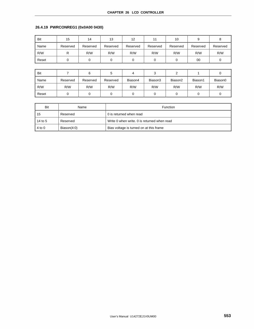
CHAPTER 26 LCD CONTROLLER
User’s Manual U14272EJ1V0UM00 553
26.4.19 PWRCONREG1 (0x0A00 0430)
Bit 15 14 13 12 11 10 9 8
Name Reserved Reserved Reserved Reserved Reserved Reserved Reserved Reserved
R/W R R/W R/W R/W R/W R/W R/W R/W
Reset 0 0 0 0 0 0 00 0
Bit 7 6 5 4 3 2 1 0
Name Reserved Reserved Reserved Biason4 Biason3 Biason2 Biason1 Biason0
R/W R/W R/W R/W R/W R/W R/W R/W R/W
Reset 0 0 0 0 0 0 0 0
Bit Name Function
15 Reserved 0 is returned when read
14 to 5 Reserved Write 0 when write. 0 is returned when read
4 to 0 Biason(4:0) Bias voltage is turned on at this frame
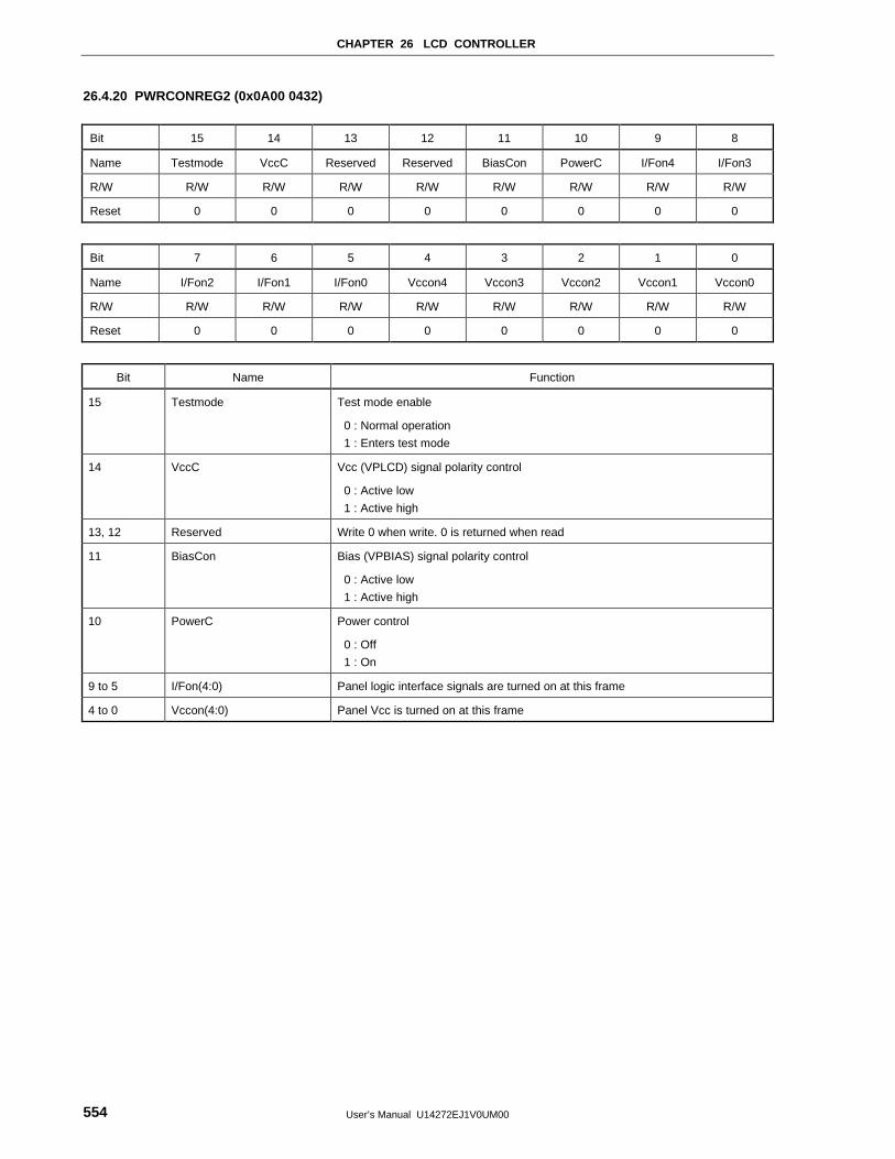
CHAPTER 26 LCD CONTROLLER
User’s Manual U14272EJ1V0UM00554
26.4.20 PWRCONREG2 (0x0A00 0432)
Bit 15 14 13 12 11 10 9 8
Name Testmode VccC Reserved Reserved BiasCon PowerC I/Fon4 I/Fon3
R/W R/W R/W R/W R/W R/W R/W R/W R/W
Reset 0 0 0 0 0 0 0 0
Bit 7 6 5 4 3 2 1 0
Name I/Fon2 I/Fon1 I/Fon0 Vccon4 Vccon3 Vccon2 Vccon1 Vccon0
R/W R/W R/W R/W R/W R/W R/W R/W R/W
Reset 0 0 0 0 0 0 0 0
Bit Name Function
15 Testmode Test mode enable
0 : Normal operation
1 : Enters test mode
14 VccC Vcc (VPLCD) signal polarity control
0 : Active low
1 : Active high
13, 12 Reserved Write 0 when write. 0 is returned when read
11 BiasCon Bias (VPBIAS) signal polarity control
0 : Active low
1 : Active high
10 PowerC Power control
0 : Off
1 : On
9 to 5 I/Fon(4:0) Panel logic interface signals are turned on at this frame
4 to 0 Vccon(4:0) Panel Vcc is turned on at this frame
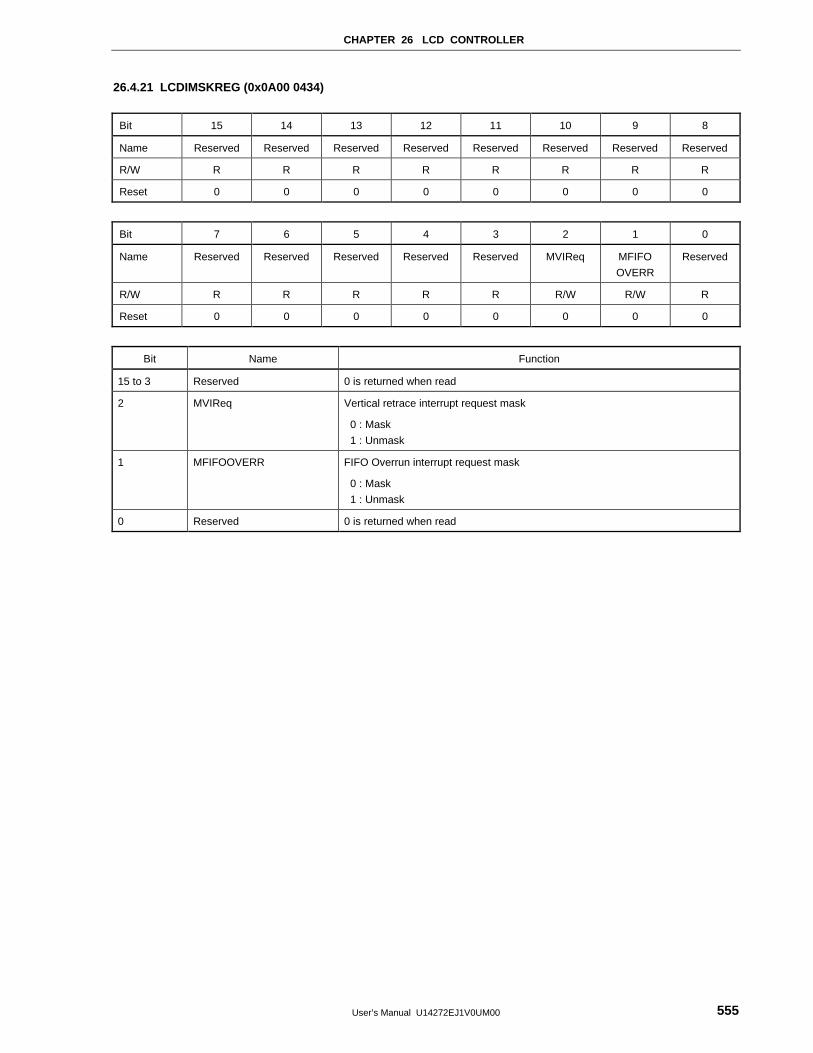
CHAPTER 26 LCD CONTROLLER
User’s Manual U14272EJ1V0UM00 555
26.4.21 LCDIMSKREG (0x0A00 0434)
Bit 15 14 13 12 11 10 9 8
Name Reserved Reserved Reserved Reserved Reserved Reserved Reserved Reserved
R/W R R R R R R R R
Reset 0 0 0 0 0 0 0 0
Bit 7 6 5 4 3 2 1 0
Name Reserved Reserved Reserved Reserved Reserved MVIReq MFIFO
OVERR
Reserved
R/W R R R R R R/W R/W R
Reset 0 0 0 0 0 0 0 0
Bit Name Function
15 to 3 Reserved 0 is returned when read
2 MVIReq Vertical retrace interrupt request mask
0 : Mask
1 : Unmask
1 MFIFOOVERR FIFO Overrun interrupt request mask
0 : Mask
1 : Unmask
0 Reserved 0 is returned when read
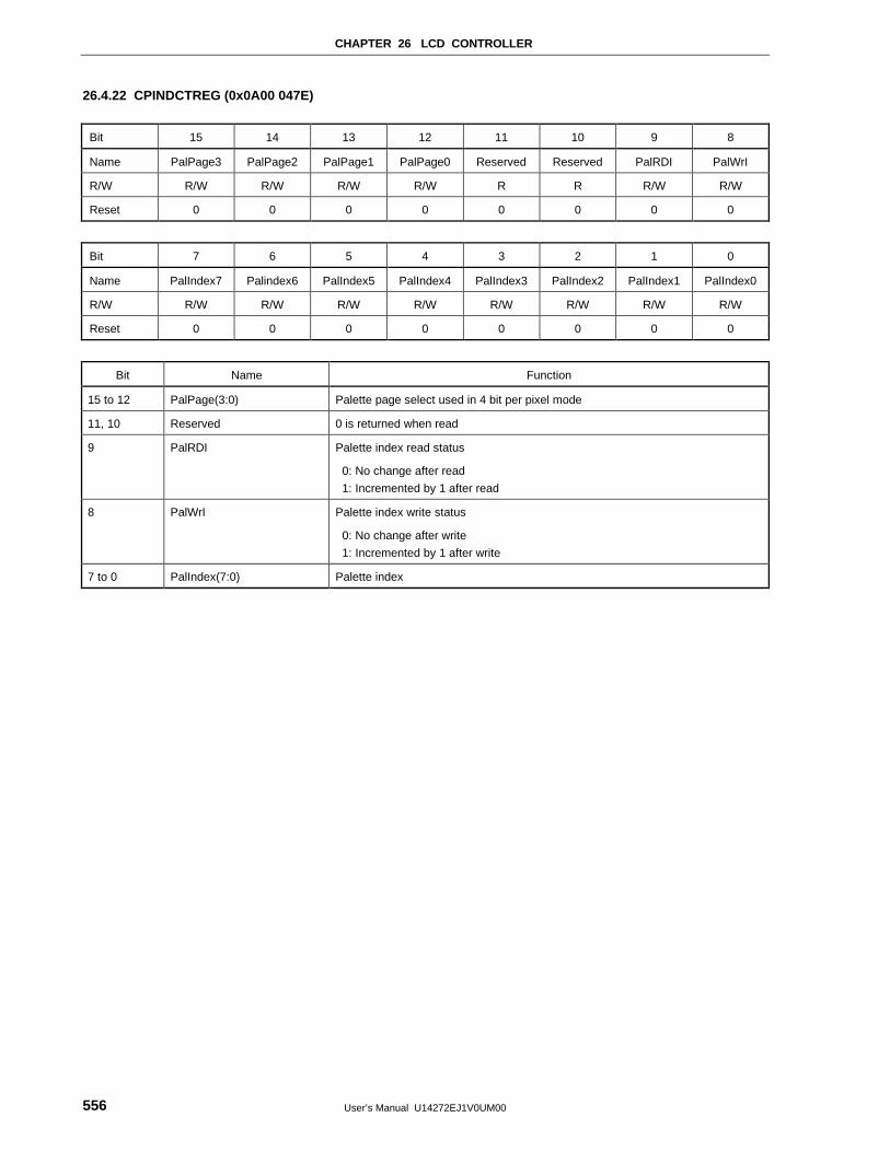
CHAPTER 26 LCD CONTROLLER
User’s Manual U14272EJ1V0UM00556
26.4.22 CPINDCTREG (0x0A00 047E)
Bit 15 14 13 12 11 10 9 8
Name PalPage3 PalPage2 PalPage1 PalPage0 Reserved Reserved PalRDI PalWrI
R/W R/W R/W R/W R/W R R R/W R/W
Reset 0 0 0 0 0 0 0 0
Bit 7 6 5 4 3 2 1 0
Name PalIndex7 Palindex6 PalIndex5 PalIndex4 PalIndex3 PalIndex2 PalIndex1 PalIndex0
R/W R/W R/W R/W R/W R/W R/W R/W R/W
Reset 0 0 0 0 0 0 0 0
Bit Name Function
15 to 12 PalPage(3:0) Palette page select used in 4 bit per pixel mode
11, 10 Reserved 0 is returned when read
9 PalRDI Palette index read status
0: No change after read
1: Incremented by 1 after read
8 PalWrI Palette index write status
0: No change after write
1: Incremented by 1 after write
7 to 0 PalIndex(7:0) Palette index
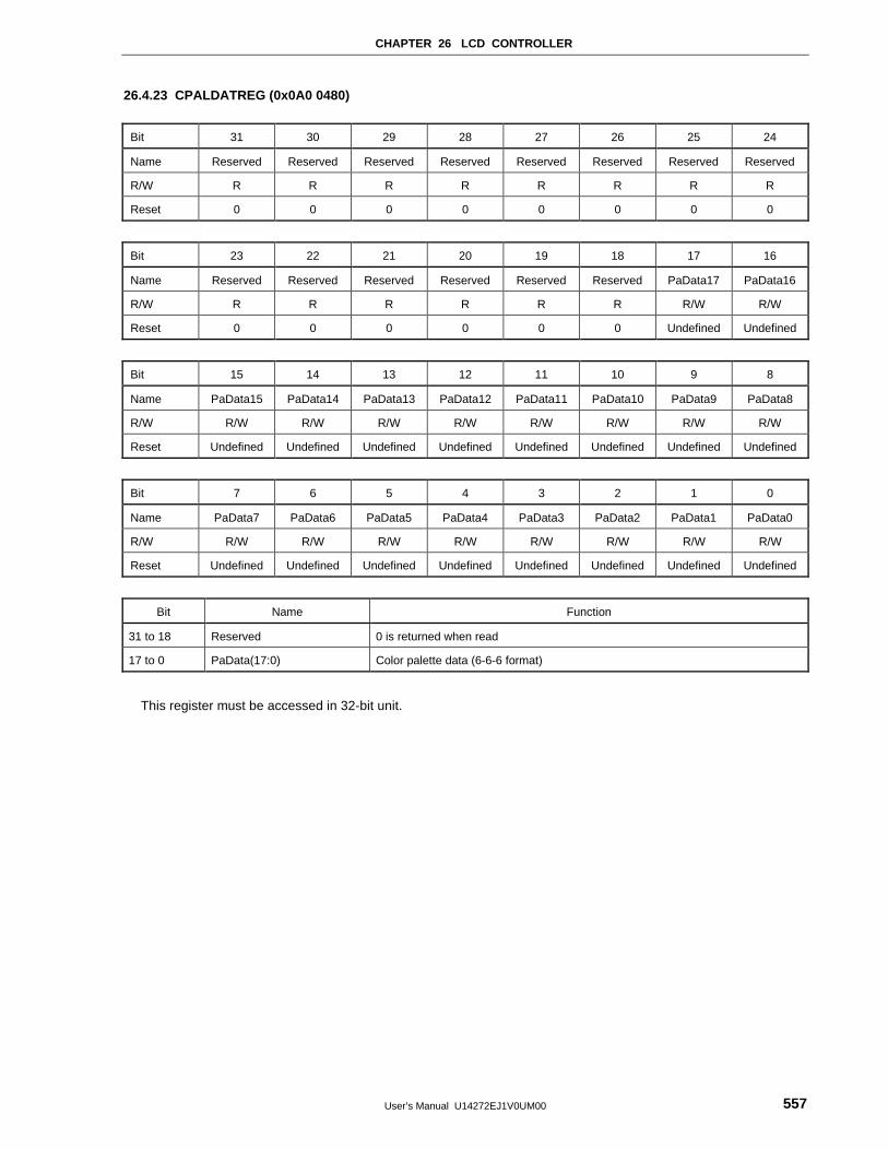
CHAPTER 26 LCD CONTROLLER
User’s Manual U14272EJ1V0UM00 557
26.4.23 CPALDATREG (0x0A0 0480)
Bit 31 30 29 28 27 26 25 24
Name Reserved Reserved Reserved Reserved Reserved Reserved Reserved Reserved
R/W R R R R R R R R
Reset 0 0 0 0 0 0 0 0
Bit 23 22 21 20 19 18 17 16
Name Reserved Reserved Reserved Reserved Reserved Reserved PaData17 PaData16
R/W R R R R R R R/W R/W
Reset 0 0 0 0 0 0 Undefined Undefined
Bit 15 14 13 12 11 10 9 8
Name PaData15 PaData14 PaData13 PaData12 PaData11 PaData10 PaData9 PaData8
R/W R/W R/W R/W R/W R/W R/W R/W R/W
Reset Undefined Undefined Undefined Undefined Undefined Undefined Undefined Undefined
Bit 7 6 5 4 3 2 1 0
Name PaData7 PaData6 PaData5 PaData4 PaData3 PaData2 PaData1 PaData0
R/W R/W R/W R/W R/W R/W R/W R/W R/W
Reset Undefined Undefined Undefined Undefined Undefined Undefined Undefined Undefined
Bit Name Function
31 to 18 Reserved 0 is returned when read
17 to 0 PaData(17:0) Color palette data (6-6-6 format)
This register must be accessed in 32-bit unit.

User’s Manual U14272EJ1V0UM00558
[MEMO]
User’s Manual U14272EJ1V0UM00 559
CHAPTER 27 MIPS III INSTRUCTION SET DETAILS
This chapter provides a detailed description of the operation of each VR4181 instruction in both 32- and 64-bit
modes. The instructions are listed in alphabetical order.
27.1 Instruction Notation Conventions
In this chapter, all variable subfields in an instruction format (such as rs, rt, immediate, etc.) are shown in
lowercase names.
For the sake of clarity, we sometimes use an alias for a variable subfield in the formats of specific instructions.
For example, we use rs = base in the format for load and store instructions. Such an alias is always lower case,
since it refers to a variable subfield.
Figures with the actual bit encoding for all the mnemonics are located at the end of this chapter (27.6 CPU
Instruction Opcode Bit Encoding ), and the bit encoding also accompanies each instruction.
In the instruction descriptions that follow, the Operation section describes the operation performed by each
instruction using a high-level language notation. The VR4181 can operate as either a 32- or 64-bit microprocessor
and the operation for both modes is included with the instruction description.
Special symbols used in the notation are described in Table 27-1.
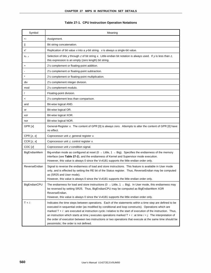
CHAPTER 27 MIPS III INSTRUCTION SET DETAILS
User’s Manual U14272EJ1V0UM00560
Table 27-1. CPU Instruction Operation Notations
Symbol Meaning
<- Assignment.
|| Bit string concatenation.
xy Replication of bit value x into a y-bit string. x is always a single-bit value.
xy…z Selection of bits y through z of bit string x. Little-endian bit notation is always used. If y is less than z,
this expression is an empty (zero length) bit string.
+ 2’s complement or floating-point addition.
- 2’s complement or floating-point subtraction.
* 2’s complement or floating-point multiplication.
div 2’s complement integer division.
mod 2’s complement modulo.
/ Floating-point division.
< 2’s complement less than comparison.
and Bit-wise logical AND.
or Bit-wise logical OR.
xor Bit-wise logical XOR.
nor Bit-wise logical NOR.
GPR [x] General-Register x. The content of GPR [0] is always zero. Attempts to alter the content of GPR [0] have
no effect.
CPR [z, x] Coprocessor unit z, general register x.
CCR [z, x] Coprocessor unit z, control register x.
COC [z] Coprocessor unit z condition signal.
BigEndianMem Big-endian mode as configured at reset (0 → Little, 1 → Big). Specifies the endianness of the memory
interface (see Table 27-2 ), and the endianness of Kernel and Supervisor mode execution.
However, this value is always 0 since the VR4181 supports the little endian order only.
ReverseEndian Signal to reverse the endianness of load and store instructions. This feature is available in User mode
only, and is effected by setting the RE bit of the Status register. Thus, ReverseEndian may be computed
as (SR25 and User mode).
However, this value is always 0 since the VR4181 supports the little endian order only.
BigEndianCPU The endianness for load and store instructions (0 → Little, 1 → Big). In User mode, this endianness may
be reversed by setting SR25. Thus, BigEndianCPU may be computed as BigEndianMem XOR
ReverseEndian.
However, this value is always 0 since the VR4181 supports the little endian order only.
T + i : Indicates the time steps between operations. Each of the statements within a time step are defined to be
executed in sequential order (as modified by conditional and loop constructs). Operations which are
marked T + i : are executed at instruction cycle i relative to the start of execution of the instruction. Thus,
an instruction which starts at time j executes operations marked T + i : at time i + j. The interpretation of
the order of execution between two instructions or two operations that execute at the same time should be
pessimistic; the order is not defined.
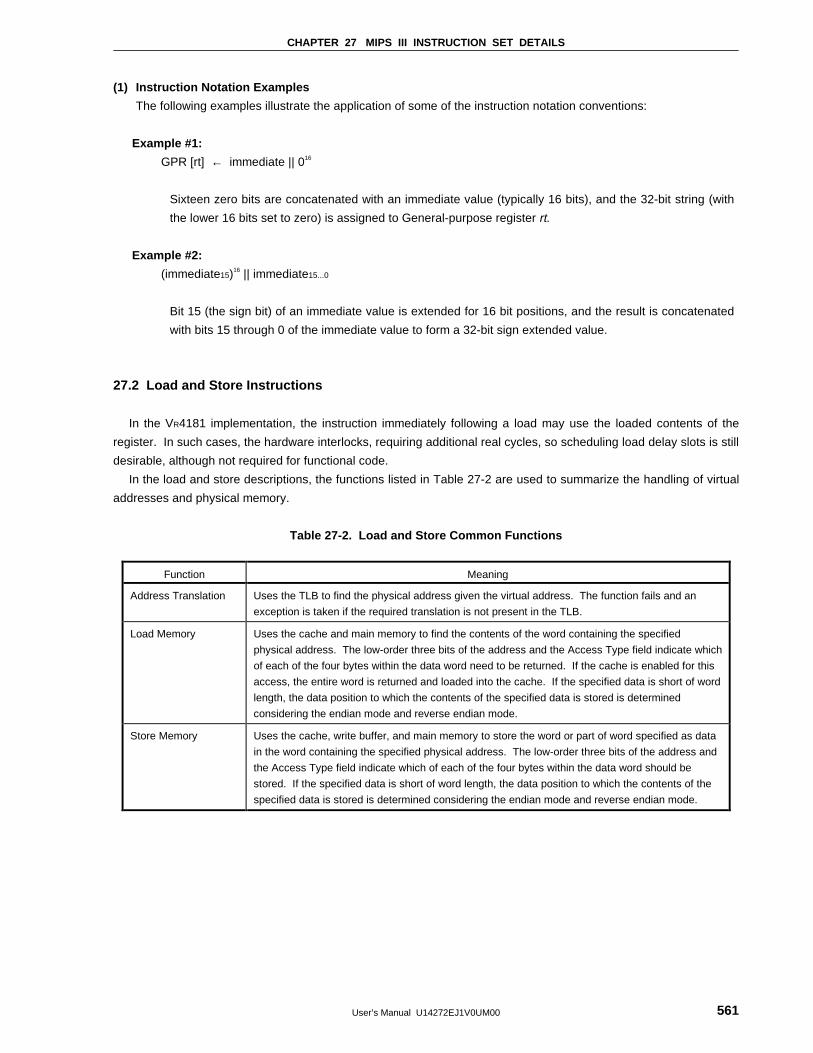
CHAPTER 27 MIPS III INSTRUCTION SET DETAILS
User’s Manual U14272EJ1V0UM00 561
(1) Instruction Notation Examples
The following examples illustrate the application of some of the instruction notation conventions:
Example #1:
GPR [rt] ← immediate || 016
Sixteen zero bits are concatenated with an immediate value (typically 16 bits), and the 32-bit string (with
the lower 16 bits set to zero) is assigned to General-purpose register rt.
Example #2:
(immediate15)16 || immediate15...0
Bit 15 (the sign bit) of an immediate value is extended for 16 bit positions, and the result is concatenated
with bits 15 through 0 of the immediate value to form a 32-bit sign extended value.
27.2 Load and Store Instructions
In the VR4181 implementation, the instruction immediately following a load may use the loaded contents of the
register. In such cases, the hardware interlocks, requiring additional real cycles, so scheduling load delay slots is still
desirable, although not required for functional code.
In the load and store descriptions, the functions listed in Table 27-2 are used to summarize the handling of virtual
addresses and physical memory.
Table 27-2. Load and Store Common Functions
Function Meaning
Address Translation Uses the TLB to find the physical address given the virtual address. The function fails and an
exception is taken if the required translation is not present in the TLB.
Load Memory Uses the cache and main memory to find the contents of the word containing the specified
physical address. The low-order three bits of the address and the Access Type field indicate which
of each of the four bytes within the data word need to be returned. If the cache is enabled for this
access, the entire word is returned and loaded into the cache. If the specified data is short of word
length, the data position to which the contents of the specified data is stored is determined
considering the endian mode and reverse endian mode.
Store Memory Uses the cache, write buffer, and main memory to store the word or part of word specified as data
in the word containing the specified physical address. The low-order three bits of the address and
the Access Type field indicate which of each of the four bytes within the data word should be
stored. If the specified data is short of word length, the data position to which the contents of the
specified data is stored is determined considering the endian mode and reverse endian mode.
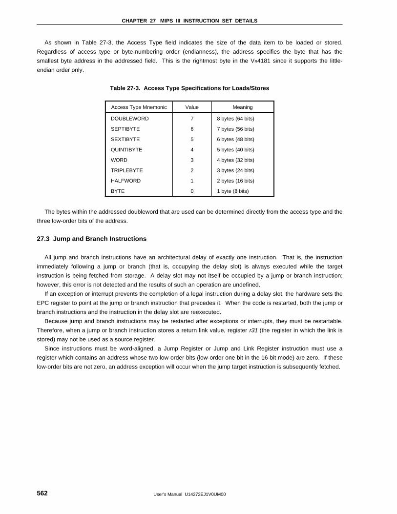
CHAPTER 27 MIPS III INSTRUCTION SET DETAILS
User’s Manual U14272EJ1V0UM00562
As shown in Table 27-3, the Access Type field indicates the size of the data item to be loaded or stored.
Regardless of access type or byte-numbering order (endianness), the address specifies the byte that has the
smallest byte address in the addressed field. This is the rightmost byte in the VR4181 since it supports the little-
endian order only.
Table 27-3. Access Type Specifications for Loads/Stores
Access Type Mnemonic Value Meaning
DOUBLEWORD
SEPTIBYTE
SEXTIBYTE
QUINTIBYTE
WORD
TRIPLEBYTE
HALFWORD
BYTE
7
6
5
4
3
2
1
0
8 bytes (64 bits)
7 bytes (56 bits)
6 bytes (48 bits)
5 bytes (40 bits)
4 bytes (32 bits)
3 bytes (24 bits)
2 bytes (16 bits)
1 byte (8 bits)
The bytes within the addressed doubleword that are used can be determined directly from the access type and the
three low-order bits of the address.
27.3 Jump and Branch Instructions
All jump and branch instructions have an architectural delay of exactly one instruction. That is, the instruction
immediately following a jump or branch (that is, occupying the delay slot) is always executed while the target
instruction is being fetched from storage. A delay slot may not itself be occupied by a jump or branch instruction;
however, this error is not detected and the results of such an operation are undefined.
If an exception or interrupt prevents the completion of a legal instruction during a delay slot, the hardware sets the
EPC register to point at the jump or branch instruction that precedes it. When the code is restarted, both the jump or
branch instructions and the instruction in the delay slot are reexecuted.
Because jump and branch instructions may be restarted after exceptions or interrupts, they must be restartable.
Therefore, when a jump or branch instruction stores a return link value, register r31 (the register in which the link is
stored) may not be used as a source register.
Since instructions must be word-aligned, a Jump Register or Jump and Link Register instruction must use a
register which contains an address whose two low-order bits (low-order one bit in the 16-bit mode) are zero. If these
low-order bits are not zero, an address exception will occur when the jump target instruction is subsequently fetched.
CHAPTER 27 MIPS III INSTRUCTION SET DETAILS
User’s Manual U14272EJ1V0UM00 563
27.4 System Control Coprocessor (CP0) Instructions
There are some special limitations imposed on operations involving CP0 that is incorporated within the CPU.
Although load and store instructions to transfer data to/from coprocessors and to move control to/from coprocessor
instructions are generally permitted by the MIPS architecture, CP0 is given a somewhat protected status since it has
responsibility for exception handling and memory management. Therefore, the move to/from coprocessor
instructions are the only valid mechanism for writing to and reading from the CP0 registers.
Several CP0 instructions are defined to directly read, write, and probe TLB entries and to modify the operating
modes in preparation for returning to User mode or interrupt-enabled states.
27.5 CPU Instruction
This section describes the functions of CPU instructions in detail for both 32-bit address mode and 64-bit address
mode.
The exception that may occur by executing each instruction is shown in the last of each instruction’s description.
For details of exceptions and their processes, see CHAPTER 7 EXCEPTION PROCESSING.
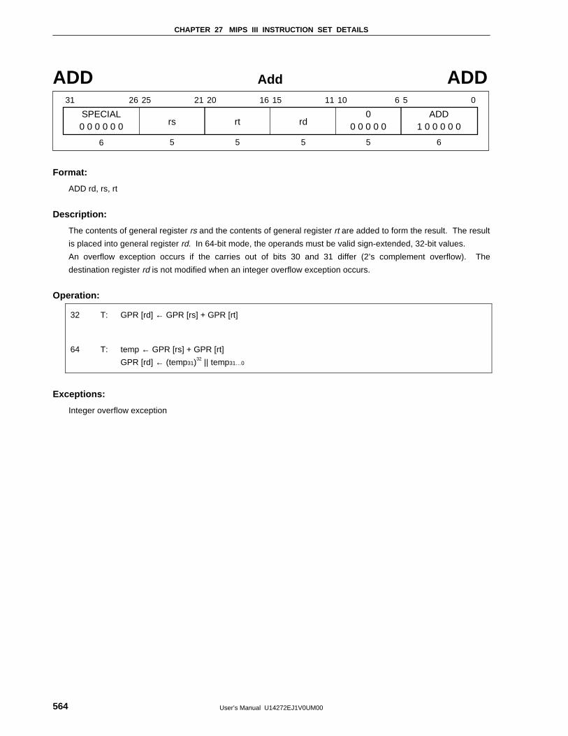
CHAPTER 27 MIPS III INSTRUCTION SET DETAILS
User’s Manual U14272EJ1V0UM00564
ADD Add ADD
SPECIAL
31 26 25 21 20 16 15 11 10 6 5 0
rs0 0 0 0 0 0 rt rd0
0 0 0 0 0ADD
1 0 0 0 0 0
6 5 5 5 5 6
Format:
ADD rd, rs, rt
Description:
The contents of general register rs and the contents of general register rt are added to form the result. The result
is placed into general register rd. In 64-bit mode, the operands must be valid sign-extended, 32-bit values.
An overflow exception occurs if the carries out of bits 30 and 31 differ (2’s complement overflow). The
destination register rd is not modified when an integer overflow exception occurs.
Operation:
32 T: GPR [rd] ← GPR [rs] + GPR [rt]
64 T: temp ← GPR [rs] + GPR [rt]
GPR [rd] ← (temp31)32 || temp31…0
Exceptions:
Integer overflow exception
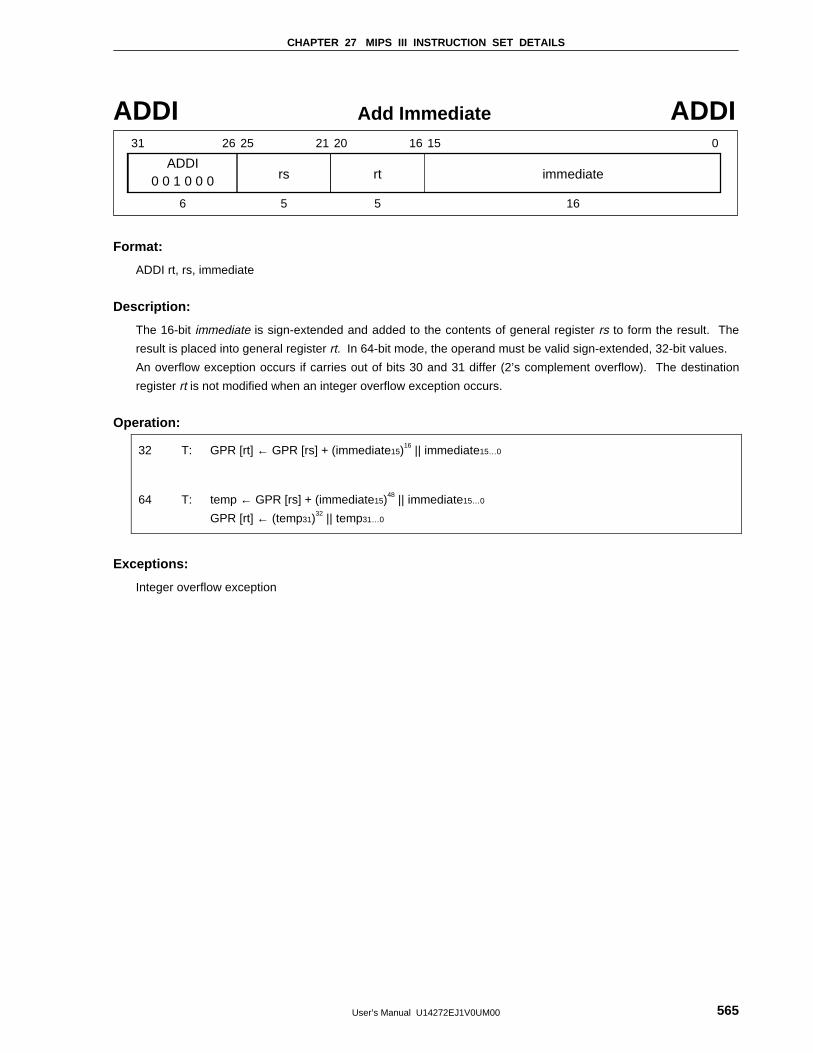
CHAPTER 27 MIPS III INSTRUCTION SET DETAILS
User’s Manual U14272EJ1V0UM00 565
ADDI Add Immediate ADDI
ADDI
31 26 25 21 20 16 15 0
rs0 0 1 0 0 0 rt immediate
6 5 5 16
Format:
ADDI rt, rs, immediate
Description:
The 16-bit immediate is sign-extended and added to the contents of general register rs to form the result. The
result is placed into general register rt. In 64-bit mode, the operand must be valid sign-extended, 32-bit values.
An overflow exception occurs if carries out of bits 30 and 31 differ (2’s complement overflow). The destination
register rt is not modified when an integer overflow exception occurs.
Operation:
32 T: GPR [rt] ← GPR [rs] + (immediate15)16 || immediate15…0
64 T: temp ← GPR [rs] + (immediate15)48 || immediate15…0
GPR [rt] ← (temp31)32 || temp31…0
Exceptions:
Integer overflow exception
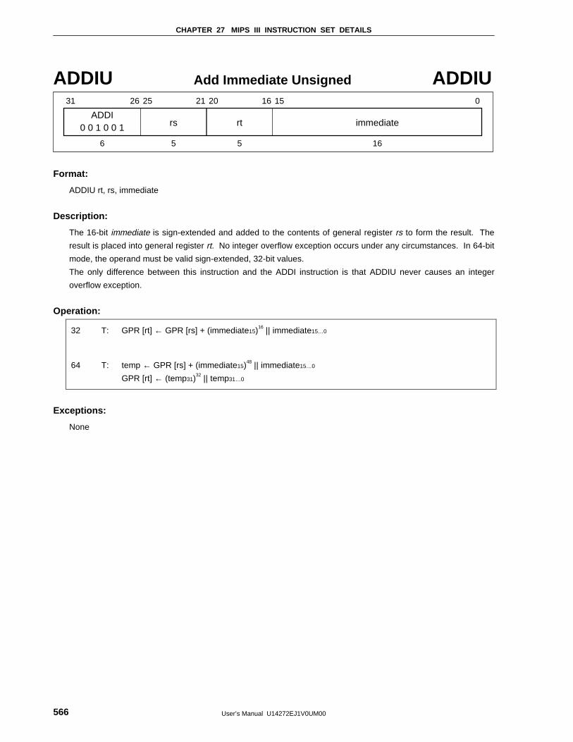
CHAPTER 27 MIPS III INSTRUCTION SET DETAILS
User’s Manual U14272EJ1V0UM00566
ADDIU Add Immediate Unsigned ADDIU
ADDI
31 26 25 21 20 16 15 0
rs0 0 1 0 0 1 rt immediate
6 5 5 16
Format:
ADDIU rt, rs, immediate
Description:
The 16-bit immediate is sign-extended and added to the contents of general register rs to form the result. The
result is placed into general register rt. No integer overflow exception occurs under any circumstances. In 64-bit
mode, the operand must be valid sign-extended, 32-bit values.
The only difference between this instruction and the ADDI instruction is that ADDIU never causes an integer
overflow exception.
Operation:
32 T: GPR [rt] ← GPR [rs] + (immediate15)16 || immediate15…0
64 T: temp ← GPR [rs] + (immediate15)48 || immediate15…0
GPR [rt] ← (temp31)32 || temp31…0
Exceptions:
None
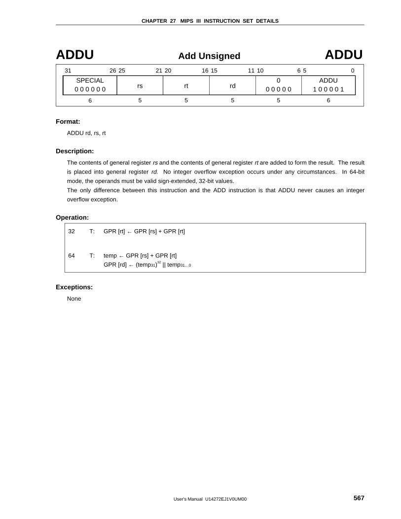
CHAPTER 27 MIPS III INSTRUCTION SET DETAILS
User’s Manual U14272EJ1V0UM00 567
ADDU Add Unsigned ADDU
SPECIAL
31 26 25 21 20 16 15 11 10 6 5 0
rs0 0 0 0 0 0 rt rd0
0 0 0 0 0ADDU
1 0 0 0 0 1
6 5 5 5 5 6
Format:
ADDU rd, rs, rt
Description:
The contents of general register rs and the contents of general register rt are added to form the result. The result
is placed into general register rd. No integer overflow exception occurs under any circumstances. In 64-bit
mode, the operands must be valid sign-extended, 32-bit values.
The only difference between this instruction and the ADD instruction is that ADDU never causes an integer
overflow exception.
Operation:
32 T: GPR [rt] ← GPR [rs] + GPR [rt]
64 T: temp ← GPR [rs] + GPR [rt]
GPR [rd] ← (temp31)32 || temp31…0
Exceptions:
None

CHAPTER 27 MIPS III INSTRUCTION SET DETAILS
User’s Manual U14272EJ1V0UM00568
AND And AND
SPECIAL
31 26 25 21 20 16 15 11 10 6 5 0
rs0 0 0 0 0 0 rt rd0
0 0 0 0 0AND
1 0 0 1 0 0
6 5 5 5 5 6
Format:
AND rd, rs, rt
Description:
The contents of general register rs are combined with the contents of general register rt in a bit-wise logical AND
operation. The result is placed into general register rd.
Operation:
32 T: GPR [rd] ← GPR [rs] and GPR [rt]
64 T: GPR [rd] ← GPR [rs] and GPR [rt]
Exceptions:
None
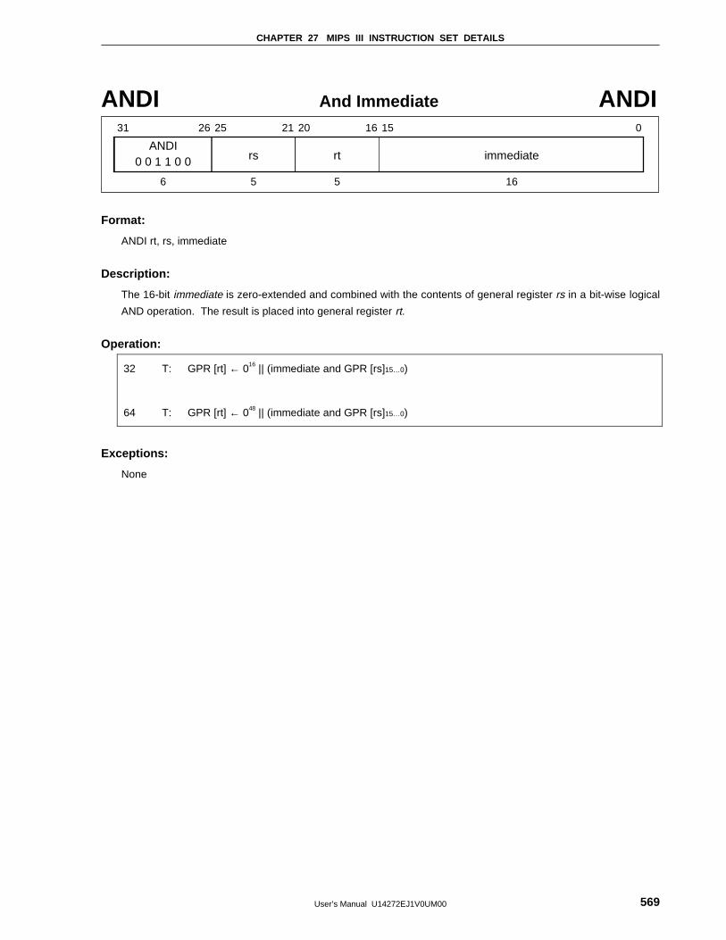
CHAPTER 27 MIPS III INSTRUCTION SET DETAILS
User’s Manual U14272EJ1V0UM00 569
ANDI And Immediate ANDI
ANDI
31 26 25 21 20 16 15 0
rs0 0 1 1 0 0 rt immediate
6 5 5 16
Format:
ANDI rt, rs, immediate
Description:
The 16-bit immediate is zero-extended and combined with the contents of general register rs in a bit-wise logical
AND operation. The result is placed into general register rt.
Operation:
32 T: GPR [rt] ← 016 || (immediate and GPR [rs]15…0)
64 T: GPR [rt] ← 048 || (immediate and GPR [rs]15…0)
Exceptions:
None
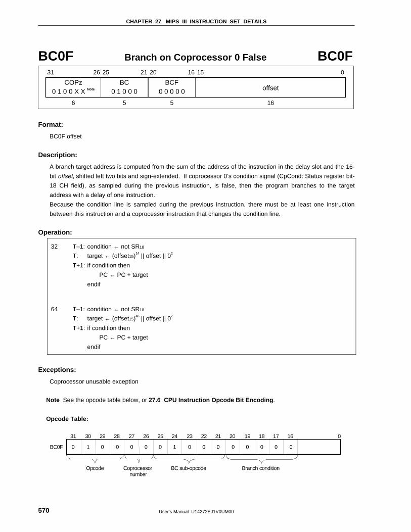
CHAPTER 27 MIPS III INSTRUCTION SET DETAILS
User’s Manual U14272EJ1V0UM00570
BC0F Branch on Coprocessor 0 False BC0F
COPz
31 26 25 21 20 16 15 0
0 1 0 0 X X Note offset
6 5 5 16
BC0 1 0 0 0
BCF0 0 0 0 0
Format:
BC0F offset
Description:
A branch target address is computed from the sum of the address of the instruction in the delay slot and the 16-
bit offset, shifted left two bits and sign-extended. If coprocessor 0’s condition signal (CpCond: Status register bit-
18 CH field), as sampled during the previous instruction, is false, then the program branches to the target
address with a delay of one instruction.
Because the condition line is sampled during the previous instruction, there must be at least one instruction
between this instruction and a coprocessor instruction that changes the condition line.
Operation:
32 T–1: condition ← not SR18
T: target ← (offset15)14 || offset || 02
T+1: if condition then
PC ← PC + target
endif
64 T–1: condition ← not SR18
T: target ← (offset15)46 || offset || 02
T+1: if condition then
PC ← PC + target
endif
Exceptions:
Coprocessor unusable exception
Note See the opcode table below, or 27.6 CPU Instruction Opcode Bit Encoding .
Opcode Table:
31
0
30
1
29
0
28
0
27
0
26
0
25
0
24
1
23
0
22
0
21
0
20
0
19
0
18
0
17
0
16
0
0
BC0F
Opcode Coprocessornumber
BC sub-opcode Branch condition
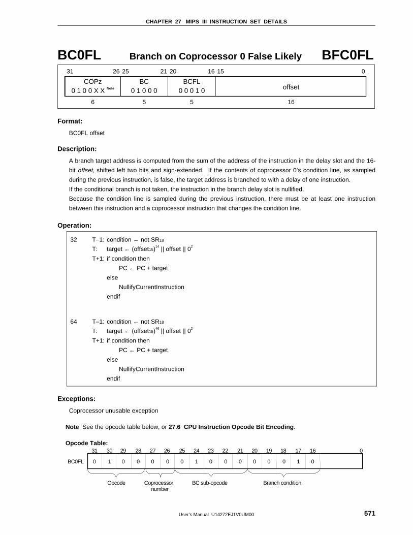
CHAPTER 27 MIPS III INSTRUCTION SET DETAILS
User’s Manual U14272EJ1V0UM00 571
BC0FL Branch on Coprocessor 0 False Likely BFC0FL
COPz
31 26 25 21 20 16 15 0
0 1 0 0 X X Note offset
6 5 5 16
BC0 1 0 0 0
BCFL0 0 0 1 0
Format:
BC0FL offset
Description:
A branch target address is computed from the sum of the address of the instruction in the delay slot and the 16-
bit offset, shifted left two bits and sign-extended. If the contents of coprocessor 0’s condition line, as sampled
during the previous instruction, is false, the target address is branched to with a delay of one instruction.
If the conditional branch is not taken, the instruction in the branch delay slot is nullified.
Because the condition line is sampled during the previous instruction, there must be at least one instruction
between this instruction and a coprocessor instruction that changes the condition line.
Operation:
32 T–1: condition ← not SR18
T: target ← (offset15)14 || offset || 02
T+1: if condition then
PC ← PC + target
else
NullifyCurrentInstruction
endif
64 T–1: condition ← not SR18
T: target ← (offset15)46 || offset || 02
T+1: if condition then
PC ← PC + target
else
NullifyCurrentInstruction
endif
Exceptions:
Coprocessor unusable exception
Note See the opcode table below, or 27.6 CPU Instruction Opcode Bit Encoding .
Opcode Table:31
0
30
1
29
0
28
0
27
0
26
0
25
0
24
1
23
0
22
0
21
0
20
0
19
0
18
0
17
1
16
0
0
BC0FL
Opcode Coprocessornumber
BC sub-opcode Branch condition
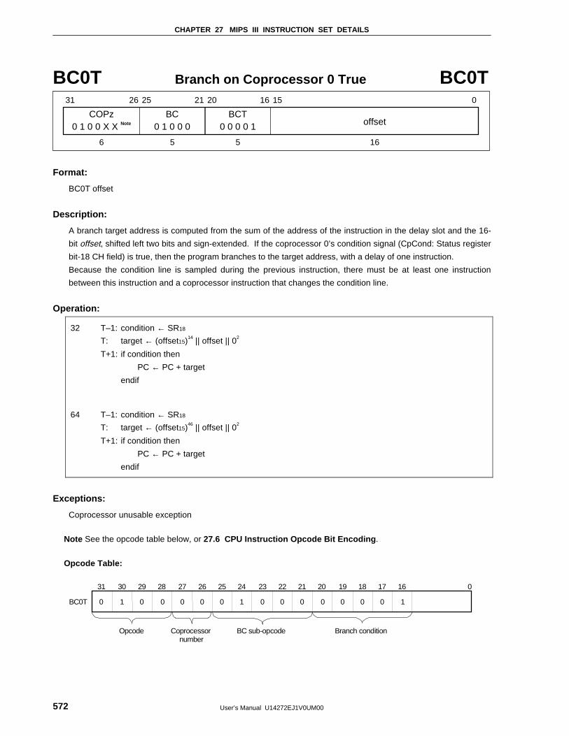
CHAPTER 27 MIPS III INSTRUCTION SET DETAILS
User’s Manual U14272EJ1V0UM00572
BC0T Branch on Coprocessor 0 True BC0T
COPz
31 26 25 21 20 16 15 0
0 1 0 0 X X Note offset
6 5 5 16
BC0 1 0 0 0
BCT0 0 0 0 1
Format:
BC0T offset
Description:
A branch target address is computed from the sum of the address of the instruction in the delay slot and the 16-
bit offset, shifted left two bits and sign-extended. If the coprocessor 0’s condition signal (CpCond: Status register
bit-18 CH field) is true, then the program branches to the target address, with a delay of one instruction.
Because the condition line is sampled during the previous instruction, there must be at least one instruction
between this instruction and a coprocessor instruction that changes the condition line.
Operation:
32 T–1: condition ← SR18
T: target ← (offset15)14 || offset || 02
T+1: if condition then
PC ← PC + target
endif
64 T–1: condition ← SR18
T: target ← (offset15)46 || offset || 02
T+1: if condition then
PC ← PC + target
endif
Exceptions:
Coprocessor unusable exception
Note See the opcode table below, or 27.6 CPU Instruction Opcode Bit Encoding .
Opcode Table:
31
0
30
1
29
0
28
0
27
0
26
0
25
0
24
1
23
0
22
0
21
0
20
0
19
0
18
0
17
0
16
1
0
BC0T
Opcode Coprocessornumber
BC sub-opcode Branch condition
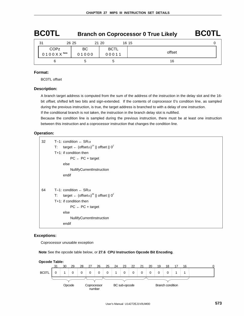
CHAPTER 27 MIPS III INSTRUCTION SET DETAILS
User’s Manual U14272EJ1V0UM00 573
BC0TL Branch on Coprocessor 0 True Likely BC0TL
COPz
31 26 25 21 20 16 15 0
0 1 0 0 X X Note offset
6 5 5 16
BC0 1 0 0 0
BCTL0 0 0 1 1
Format:
BC0TL offset
Description:
A branch target address is computed from the sum of the address of the instruction in the delay slot and the 16-
bit offset, shifted left two bits and sign-extended. If the contents of coprocessor 0’s condition line, as sampled
during the previous instruction, is true, the target address is branched to with a delay of one instruction.
If the conditional branch is not taken, the instruction in the branch delay slot is nullified.
Because the condition line is sampled during the previous instruction, there must be at least one instruction
between this instruction and a coprocessor instruction that changes the condition line.
Operation:
32 T–1: condition ← SR18
T: target ← (offset15)14 || offset || 02
T+1: if condition then
PC ← PC + target
else
NullifyCurrentInstruction
endif
64 T–1: condition ← SR18
T: target ← (offset15)46 || offset || 02
T+1: if condition then
PC ← PC + target
else
NullifyCurrentInstruction
endif
Exceptions:
Coprocessor unusable exception
Note See the opcode table below, or 27.6 CPU Instruction Opcode Bit Encoding .
Opcode Table:31
0
30
1
29
0
28
0
27
0
26
0
25
0
24
1
23
0
22
0
21
0
20
0
19
0
18
0
17
1
16
1
0
BC0TL
Opcode Coprocessornumber
BC sub-opcode Branch condition
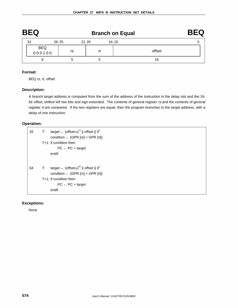
CHAPTER 27 MIPS III INSTRUCTION SET DETAILS
User’s Manual U14272EJ1V0UM00574
BEQ Branch on Equal BEQ
BEQ
31 26 25 21 20 16 15 0
rs0 0 0 1 0 0 rt offset
6 5 5 16
Format:
BEQ rs, rt, offset
Description:
A branch target address is computed from the sum of the address of the instruction in the delay slot and the 16-
bit offset, shifted left two bits and sign-extended. The contents of general register rs and the contents of general
register rt are compared. If the two registers are equal, then the program branches to the target address, with a
delay of one instruction.
Operation:
32 T: target ← (offset15)14 || offset || 02
condition ← (GPR [rs] = GPR [rt])
T+1: if condition then
PC ← PC + target
endif
64 T: target ← (offset15)46 || offset || 02
condition ← (GPR [rs] = GPR [rt])
T+1: if condition then
PC ← PC + target
endif
Exceptions:
None
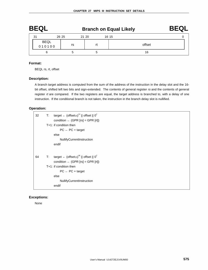
CHAPTER 27 MIPS III INSTRUCTION SET DETAILS
User’s Manual U14272EJ1V0UM00 575
BEQL Branch on Equal Likely BEQL
BEQL
31 26 25 21 20 16 15 0
rs0 1 0 1 0 0 rt offset
6 5 5 16
Format:
BEQL rs, rt, offset
Description:
A branch target address is computed from the sum of the address of the instruction in the delay slot and the 16-
bit offset, shifted left two bits and sign-extended. The contents of general register rs and the contents of general
register rt are compared. If the two registers are equal, the target address is branched to, with a delay of one
instruction. If the conditional branch is not taken, the instruction in the branch delay slot is nullified.
Operation:
32 T: target ← (offset15)14 || offset || 02
condition ← (GPR [rs] = GPR [rt])
T+1: if condition then
PC ← PC + target
else
NullifyCurrentInstruction
endif
64 T: target ← (offset15)46 || offset || 02
condition ← (GPR [rs] = GPR [rt])
T+1: if condition then
PC ← PC + target
else
NullifyCurrentInstruction
endif
Exceptions:
None
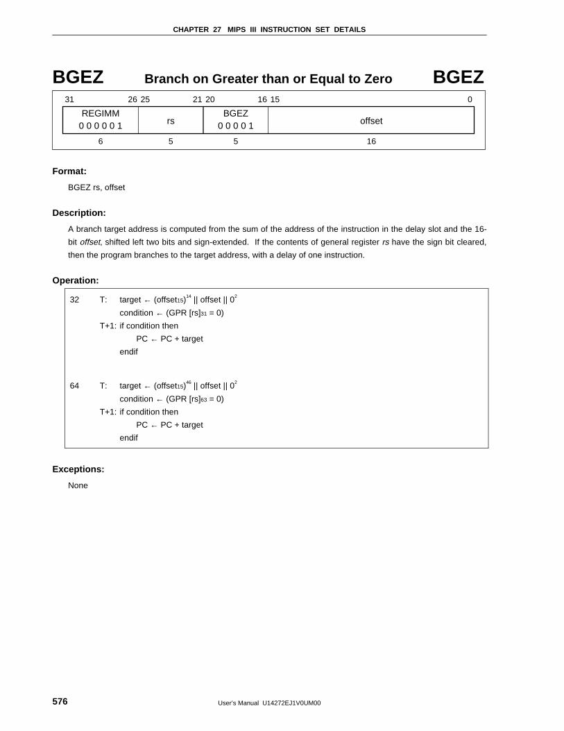
CHAPTER 27 MIPS III INSTRUCTION SET DETAILS
User’s Manual U14272EJ1V0UM00576
BGEZ Branch on Greater than or Equal to Zero BGEZ
REGIMM
31 26 25 21 20 16 15 0
rs0 0 0 0 0 1 offset
6 5 5 16
BGEZ0 0 0 0 1
Format:
BGEZ rs, offset
Description:
A branch target address is computed from the sum of the address of the instruction in the delay slot and the 16-
bit offset, shifted left two bits and sign-extended. If the contents of general register rs have the sign bit cleared,
then the program branches to the target address, with a delay of one instruction.
Operation:
32 T: target ← (offset15)14 || offset || 02
condition ← (GPR [rs]31 = 0)
T+1: if condition then
PC ← PC + target
endif
64 T: target ← (offset15)46 || offset || 02
condition ← (GPR [rs]63 = 0)
T+1: if condition then
PC ← PC + target
endif
Exceptions:
None
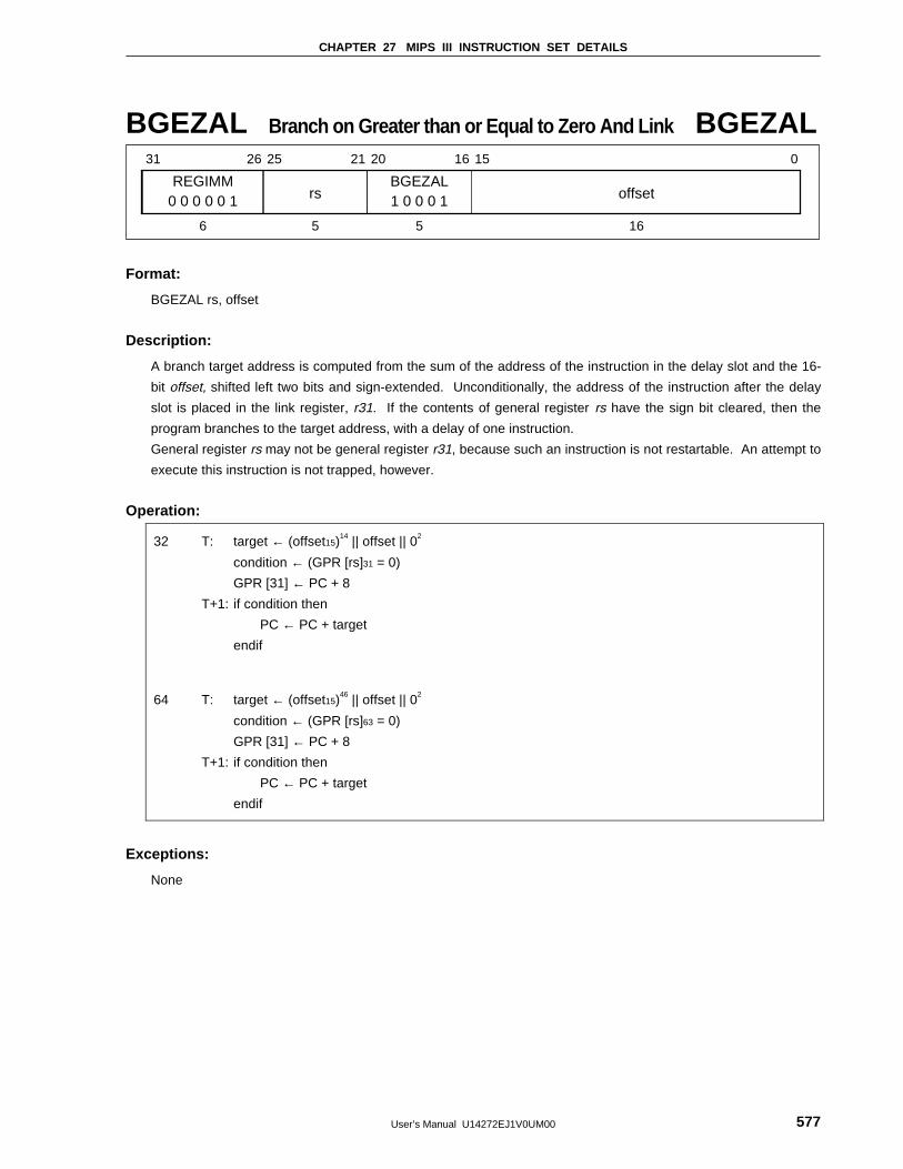
CHAPTER 27 MIPS III INSTRUCTION SET DETAILS
User’s Manual U14272EJ1V0UM00 577
BGEZAL Branch on Greater than or Equal to Zero And Link BGEZAL
REGIMM
31 26 25 21 20 16 15 0
rs0 0 0 0 0 1 offset
6 5 5 16
BGEZAL1 0 0 0 1
Format:
BGEZAL rs, offset
Description:
A branch target address is computed from the sum of the address of the instruction in the delay slot and the 16-
bit offset, shifted left two bits and sign-extended. Unconditionally, the address of the instruction after the delay
slot is placed in the link register, r31. If the contents of general register rs have the sign bit cleared, then the
program branches to the target address, with a delay of one instruction.
General register rs may not be general register r31, because such an instruction is not restartable. An attempt to
execute this instruction is not trapped, however.
Operation:
32 T: target ← (offset15)14 || offset || 02
condition ← (GPR [rs]31 = 0)
GPR [31] ← PC + 8
T+1: if condition then
PC ← PC + target
endif
64 T: target ← (offset15)46 || offset || 02
condition ← (GPR [rs]63 = 0)
GPR [31] ← PC + 8
T+1: if condition then
PC ← PC + target
endif
Exceptions:
None
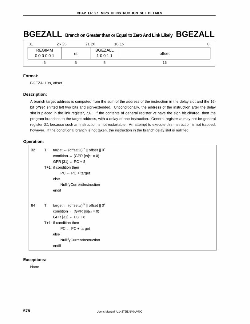
CHAPTER 27 MIPS III INSTRUCTION SET DETAILS
User’s Manual U14272EJ1V0UM00578
BGEZALL Branch on Greater than or Equal to Zero And Link Likely BGEZALL
REGIMM
31 26 25 21 20 16 15 0
rs0 0 0 0 0 1 offset
6 5 5 16
BGEZALL1 0 0 1 1
Format:
BGEZALL rs, offset
Description:
A branch target address is computed from the sum of the address of the instruction in the delay slot and the 16-
bit offset, shifted left two bits and sign-extended. Unconditionally, the address of the instruction after the delay
slot is placed in the link register, r31. If the contents of general register rs have the sign bit cleared, then the
program branches to the target address, with a delay of one instruction. General register rs may not be general
register 31, because such an instruction is not restartable. An attempt to execute this instruction is not trapped,
however. If the conditional branch is not taken, the instruction in the branch delay slot is nullified.
Operation:
32 T: target ← (offset15)14 || offset || 02
condition ← (GPR [rs]31 = 0)
GPR [31] ← PC + 8
T+1: if condition then
PC ← PC + target
else
NullifyCurrentInstruction
endif
64 T: target ← (offset15)46 || offset || 02
condition ← (GPR [rs]63 = 0)
GPR [31] ← PC + 8
T+1: if condition then
PC ← PC + target
else
NullifyCurrentInstruction
endif
Exceptions:
None
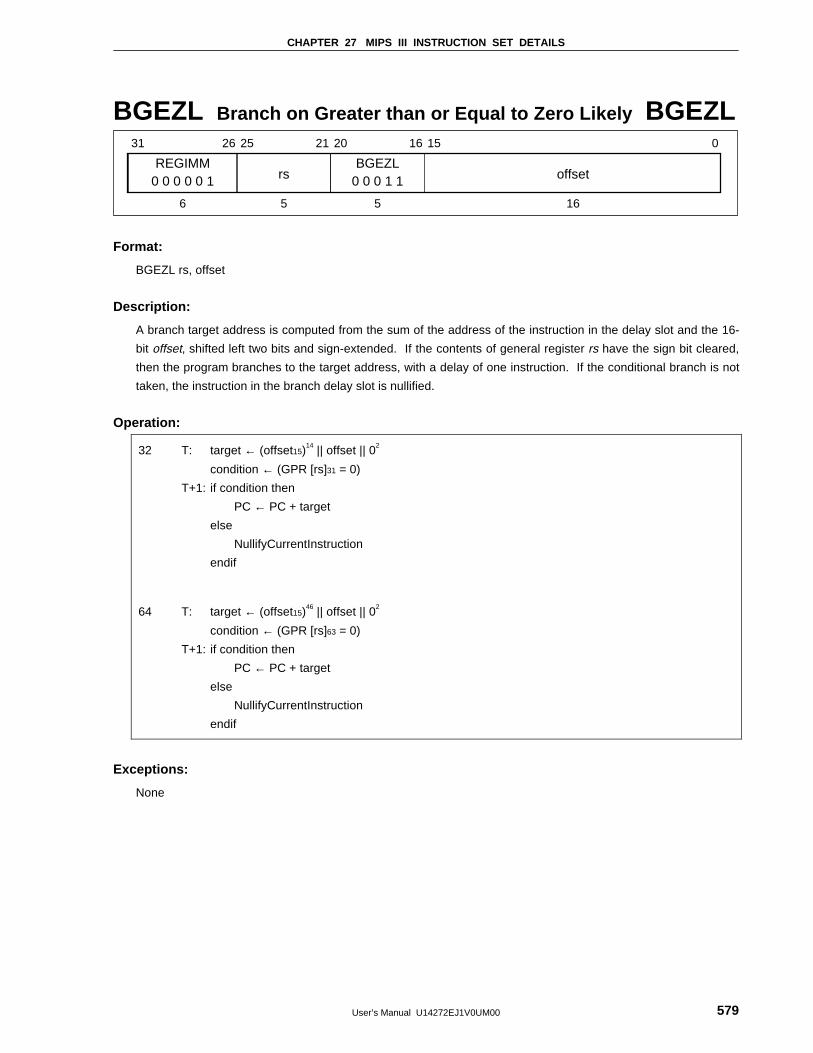
CHAPTER 27 MIPS III INSTRUCTION SET DETAILS
User’s Manual U14272EJ1V0UM00 579
BGEZL Branch on Greater than or Equal to Zero Likely BGEZL
REGIMM
31 26 25 21 20 16 15 0
rs0 0 0 0 0 1 offset
6 5 5 16
BGEZL0 0 0 1 1
Format:
BGEZL rs, offset
Description:
A branch target address is computed from the sum of the address of the instruction in the delay slot and the 16-
bit offset, shifted left two bits and sign-extended. If the contents of general register rs have the sign bit cleared,
then the program branches to the target address, with a delay of one instruction. If the conditional branch is not
taken, the instruction in the branch delay slot is nullified.
Operation:
32 T: target ← (offset15)14 || offset || 02
condition ← (GPR [rs]31 = 0)
T+1: if condition then
PC ← PC + target
else
NullifyCurrentInstruction
endif
64 T: target ← (offset15)46 || offset || 02
condition ← (GPR [rs]63 = 0)
T+1: if condition then
PC ← PC + target
else
NullifyCurrentInstruction
endif
Exceptions:
None
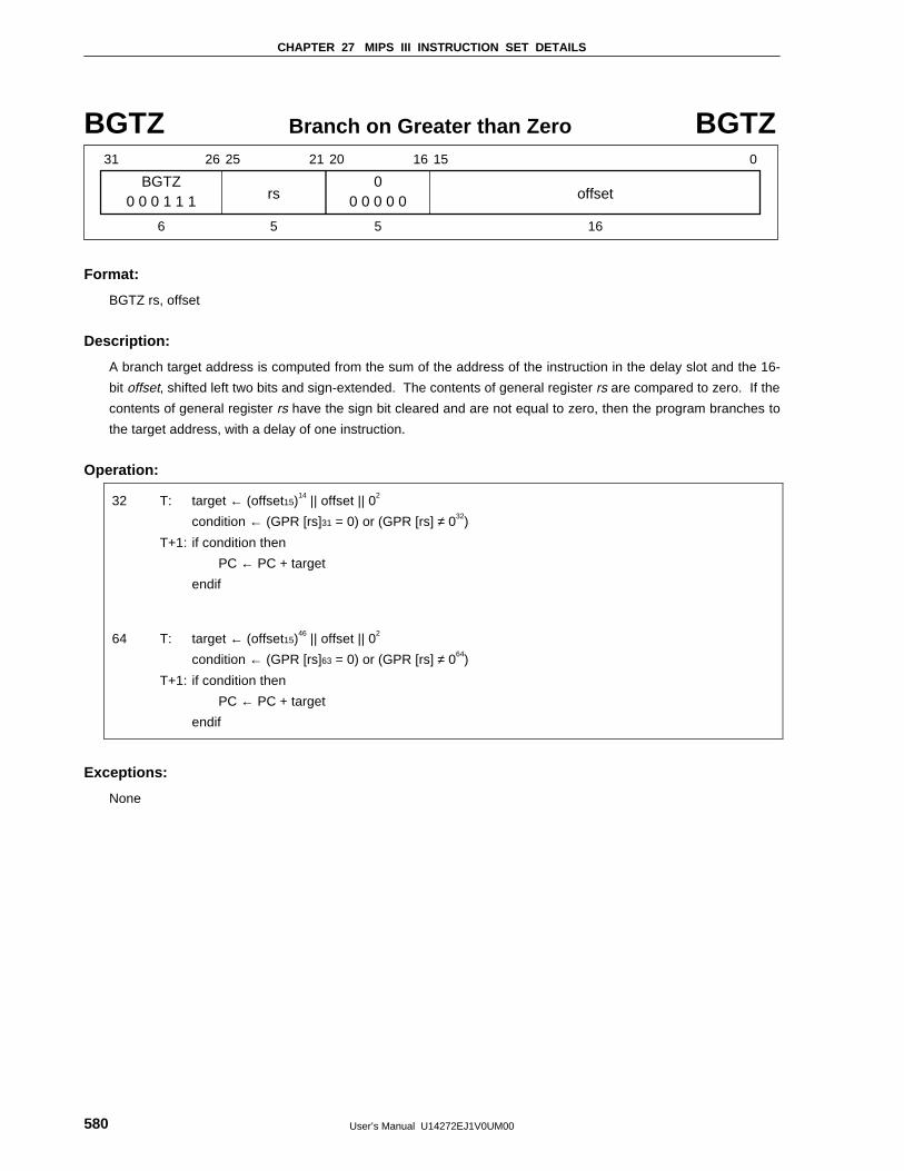
CHAPTER 27 MIPS III INSTRUCTION SET DETAILS
User’s Manual U14272EJ1V0UM00580
BGTZ Branch on Greater than Zero BGTZ
BGTZ
31 26 25 21 20 16 15 0
rs0 0 0 1 1 1 offset
6 5 5 16
00 0 0 0 0
Format:
BGTZ rs, offset
Description:
A branch target address is computed from the sum of the address of the instruction in the delay slot and the 16-
bit offset, shifted left two bits and sign-extended. The contents of general register rs are compared to zero. If the
contents of general register rs have the sign bit cleared and are not equal to zero, then the program branches to
the target address, with a delay of one instruction.
Operation:
32 T: target ← (offset15)14 || offset || 02
condition ← (GPR [rs]31 = 0) or (GPR [rs] ≠ 032)
T+1: if condition then
PC ← PC + target
endif
64 T: target ← (offset15)46 || offset || 02
condition ← (GPR [rs]63 = 0) or (GPR [rs] ≠ 064)
T+1: if condition then
PC ← PC + target
endif
Exceptions:
None
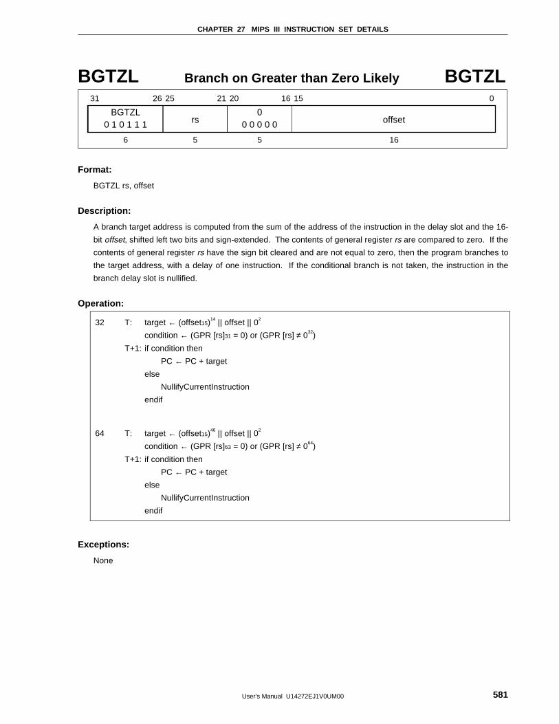
CHAPTER 27 MIPS III INSTRUCTION SET DETAILS
User’s Manual U14272EJ1V0UM00 581
BGTZL Branch on Greater than Zero Likely BGTZL
BGTZL
31 26 25 21 20 16 15 0
rs0 1 0 1 1 1 offset
6 5 5 16
00 0 0 0 0
Format:
BGTZL rs, offset
Description:
A branch target address is computed from the sum of the address of the instruction in the delay slot and the 16-
bit offset, shifted left two bits and sign-extended. The contents of general register rs are compared to zero. If the
contents of general register rs have the sign bit cleared and are not equal to zero, then the program branches to
the target address, with a delay of one instruction. If the conditional branch is not taken, the instruction in the
branch delay slot is nullified.
Operation:
32 T: target ← (offset15)14 || offset || 02
condition ← (GPR [rs]31 = 0) or (GPR [rs] ≠ 032)
T+1: if condition then
PC ← PC + target
else
NullifyCurrentInstruction
endif
64 T: target ← (offset15)46 || offset || 02
condition ← (GPR [rs]63 = 0) or (GPR [rs] ≠ 064)
T+1: if condition then
PC ← PC + target
else
NullifyCurrentInstruction
endif
Exceptions:
None
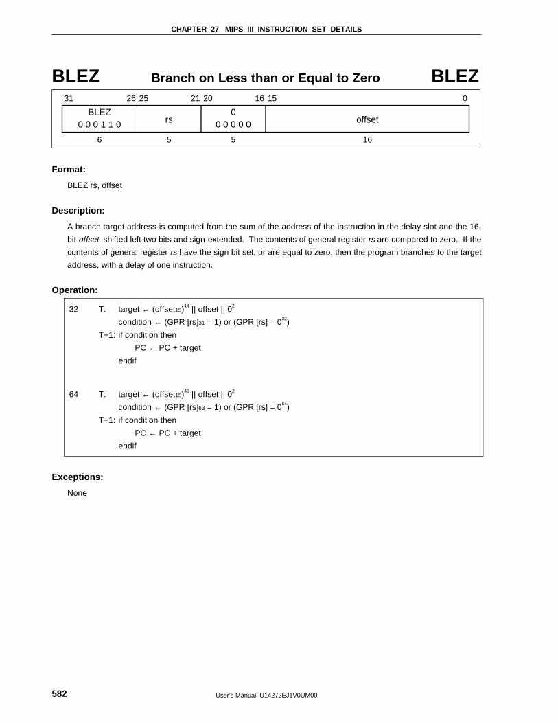
CHAPTER 27 MIPS III INSTRUCTION SET DETAILS
User’s Manual U14272EJ1V0UM00582
BLEZ Branch on Less than or Equal to Zero BLEZ
BLEZ
31 26 25 21 20 16 15 0
rs0 0 0 1 1 0 offset
6 5 5 16
00 0 0 0 0
Format:
BLEZ rs, offset
Description:
A branch target address is computed from the sum of the address of the instruction in the delay slot and the 16-
bit offset, shifted left two bits and sign-extended. The contents of general register rs are compared to zero. If the
contents of general register rs have the sign bit set, or are equal to zero, then the program branches to the target
address, with a delay of one instruction.
Operation:
32 T: target ← (offset15)14 || offset || 02
condition ← (GPR [rs]31 = 1) or (GPR [rs] = 032)
T+1: if condition then
PC ← PC + target
endif
64 T: target ← (offset15)46 || offset || 02
condition ← (GPR [rs]63 = 1) or (GPR [rs] = 064)
T+1: if condition then
PC ← PC + target
endif
Exceptions:
None
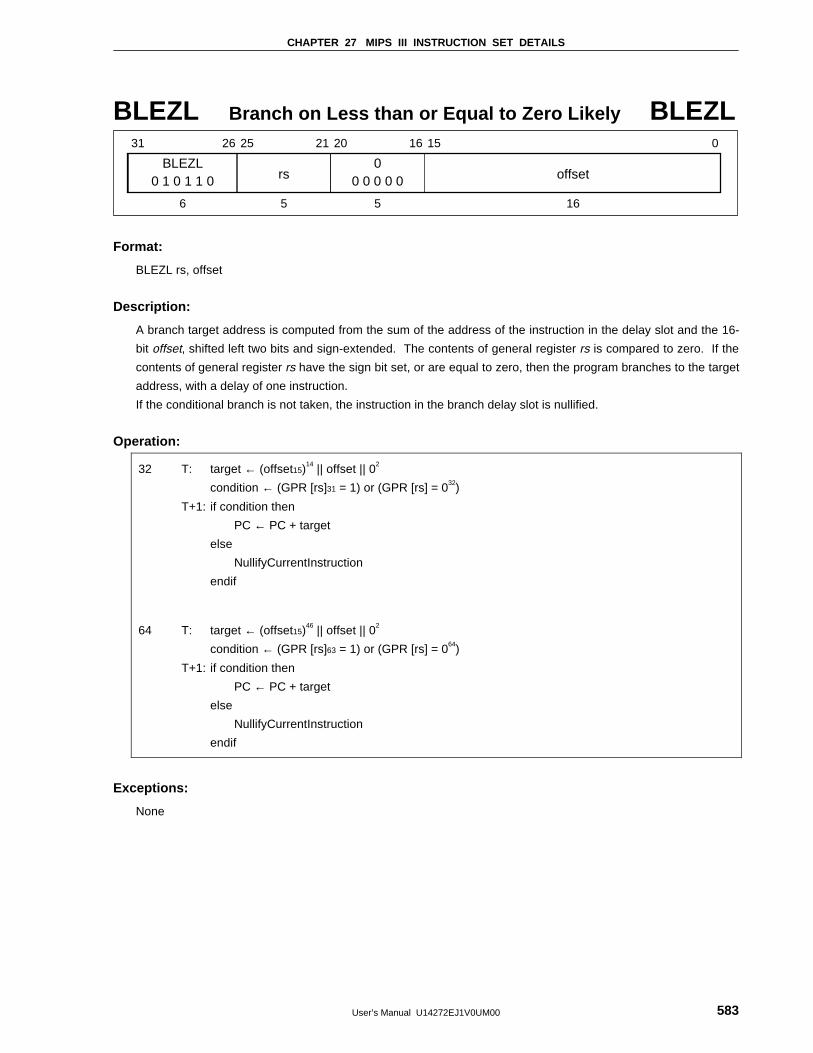
CHAPTER 27 MIPS III INSTRUCTION SET DETAILS
User’s Manual U14272EJ1V0UM00 583
BLEZL Branch on Less than or Equal to Zero Likely BLEZL
BLEZL
31 26 25 21 20 16 15 0
rs0 1 0 1 1 0 offset
6 5 5 16
00 0 0 0 0
Format:
BLEZL rs, offset
Description:
A branch target address is computed from the sum of the address of the instruction in the delay slot and the 16-
bit offset, shifted left two bits and sign-extended. The contents of general register rs is compared to zero. If the
contents of general register rs have the sign bit set, or are equal to zero, then the program branches to the target
address, with a delay of one instruction.
If the conditional branch is not taken, the instruction in the branch delay slot is nullified.
Operation:
32 T: target ← (offset15)14 || offset || 02
condition ← (GPR [rs]31 = 1) or (GPR [rs] = 032)
T+1: if condition then
PC ← PC + target
else
NullifyCurrentInstruction
endif
64 T: target ← (offset15)46 || offset || 02
condition ← (GPR [rs]63 = 1) or (GPR [rs] = 064)
T+1: if condition then
PC ← PC + target
else
NullifyCurrentInstruction
endif
Exceptions:
None

CHAPTER 27 MIPS III INSTRUCTION SET DETAILS
User’s Manual U14272EJ1V0UM00584
BLTZ Branch on Less than Zero BLTZ
REGIMM
31 26 25 21 20 16 15 0
rs0 0 0 0 0 1 offset
6 5 5 16
BLTZ0 0 0 0 0
Format:
BLTZ rs, offset
Description:
A branch target address is computed from the sum of the address of the instruction in the delay slot and the 16-
bit offset, shifted left two bits and sign-extended. If the contents of general register rs have the sign bit set, then
the program branches to the target address, with a delay of one instruction.
Operation:
32 T: target ← (offset15)14 || offset || 02
condition ← (GPR [rs]31 = 1)
T+1: if condition then
PC ← PC + target
endif
64 T: target ← (offset15)46 || offset || 02
condition ← (GPR [rs]63 = 1)
T+1: if condition then
PC ← PC + target
endif
Exceptions:
None

CHAPTER 27 MIPS III INSTRUCTION SET DETAILS
User’s Manual U14272EJ1V0UM00 585
BLTZAL Branch on Less than Zero and Link BLTZAL
REGIMM
31 26 25 21 20 16 15 0
rs0 0 0 0 0 1 offset
6 5 5 16
BLTZAL1 0 0 0 0
Format:
BLTZAL rs, offset
Description:
A branch target address is computed from the sum of the address of the instruction in the delay slot and the 16-
bit offset, shifted left two bits and sign-extended. Unconditionally, the address of the instruction after the delay
slot is placed in the link register, r31. If the contents of general register rs have the sign bit set, then the program
branches to the target address, with a delay of one instruction.
General register rs may not be general register 31, because such an instruction is not restartable. An attempt to
execute this instruction with register 31 specified as rs is not trapped, however.
Operation:
32 T: target ← (offset15)14 || offset || 02
condition ← (GPR [rs]31 = 1)
GPR [31] ← PC + 8
T+1: if condition then
PC ← PC + target
endif
64 T: target ← (offset15)46 || offset || 02
condition ← (GPR [rs]63 = 1)
GPR [31] ← PC + 8
T+1: if condition then
PC ← PC + target
endif
Exceptions:
None
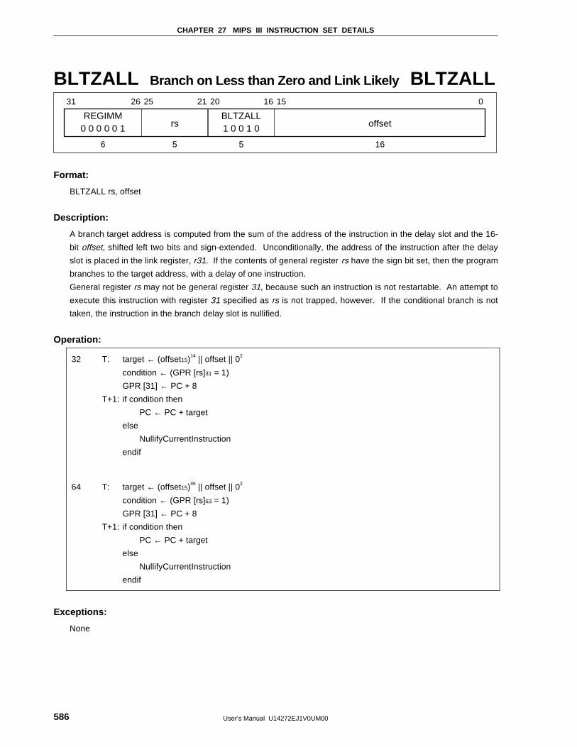
CHAPTER 27 MIPS III INSTRUCTION SET DETAILS
User’s Manual U14272EJ1V0UM00586
BLTZALL Branch on Less than Zero and Link Likely BLTZALL
REGIMM
31 26 25 21 20 16 15 0
rs0 0 0 0 0 1 offset
6 5 5 16
BLTZALL1 0 0 1 0
Format:
BLTZALL rs, offset
Description:
A branch target address is computed from the sum of the address of the instruction in the delay slot and the 16-
bit offset, shifted left two bits and sign-extended. Unconditionally, the address of the instruction after the delay
slot is placed in the link register, r31. If the contents of general register rs have the sign bit set, then the program
branches to the target address, with a delay of one instruction.
General register rs may not be general register 31, because such an instruction is not restartable. An attempt to
execute this instruction with register 31 specified as rs is not trapped, however. If the conditional branch is not
taken, the instruction in the branch delay slot is nullified.
Operation:
32 T: target ← (offset15)14 || offset || 02
condition ← (GPR [rs]31 = 1)
GPR [31] ← PC + 8
T+1: if condition then
PC ← PC + target
else
NullifyCurrentInstruction
endif
64 T: target ← (offset15)46 || offset || 02
condition ← (GPR [rs]63 = 1)
GPR [31] ← PC + 8
T+1: if condition then
PC ← PC + target
else
NullifyCurrentInstruction
endif
Exceptions:
None
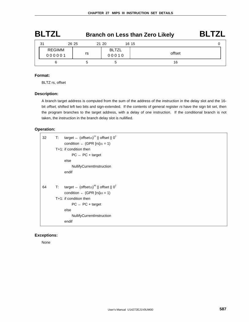
CHAPTER 27 MIPS III INSTRUCTION SET DETAILS
User’s Manual U14272EJ1V0UM00 587
BLTZL Branch on Less than Zero Likely BLTZL
REGIMM
31 26 25 21 20 16 15 0
rs0 0 0 0 0 1 offset
6 5 5 16
BLTZL0 0 0 1 0
Format:
BLTZ rs, offset
Description:
A branch target address is computed from the sum of the address of the instruction in the delay slot and the 16-
bit offset, shifted left two bits and sign-extended. If the contents of general register rs have the sign bit set, then
the program branches to the target address, with a delay of one instruction. If the conditional branch is not
taken, the instruction in the branch delay slot is nullified.
Operation:
32 T: target ← (offset15)14 || offset || 02
condition ← (GPR [rs]31 = 1)
T+1: if condition then
PC ← PC + target
else
NullifyCurrentInstruction
endif
64 T: target ← (offset15)46 || offset || 02
condition ← (GPR [rs]63 = 1)
T+1: if condition then
PC ← PC + target
else
NullifyCurrentInstruction
endif
Exceptions:
None
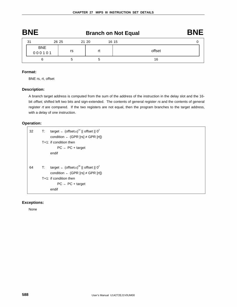
CHAPTER 27 MIPS III INSTRUCTION SET DETAILS
User’s Manual U14272EJ1V0UM00588
BNE Branch on Not Equal BNE
BNE
31 26 25 21 20 16 15 0
rs0 0 0 1 0 1 rt offset
6 5 5 16
Format:
BNE rs, rt, offset
Description:
A branch target address is computed from the sum of the address of the instruction in the delay slot and the 16-
bit offset, shifted left two bits and sign-extended. The contents of general register rs and the contents of general
register rt are compared. If the two registers are not equal, then the program branches to the target address,
with a delay of one instruction.
Operation:
32 T: target ← (offset15)14 || offset || 02
condition ← (GPR [rs] ≠ GPR [rt])
T+1: if condition then
PC ← PC + target
endif
64 T: target ← (offset15)46 || offset || 02
condition ← (GPR [rs] ≠ GPR [rt])
T+1: if condition then
PC ← PC + target
endif
Exceptions:
None
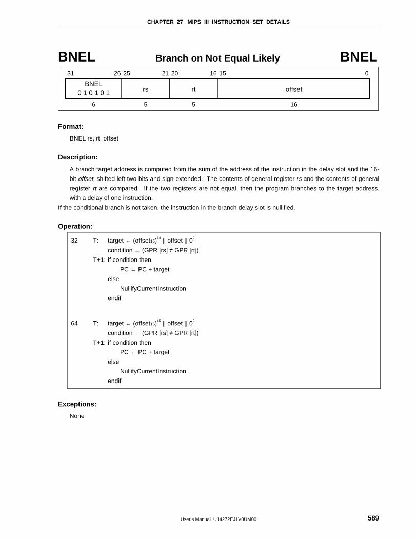
CHAPTER 27 MIPS III INSTRUCTION SET DETAILS
User’s Manual U14272EJ1V0UM00 589
BNEL Branch on Not Equal Likely BNEL
BNEL
31 26 25 21 20 16 15 0
rs0 1 0 1 0 1 rt offset
6 5 5 16
Format:
BNEL rs, rt, offset
Description:
A branch target address is computed from the sum of the address of the instruction in the delay slot and the 16-
bit offset, shifted left two bits and sign-extended. The contents of general register rs and the contents of general
register rt are compared. If the two registers are not equal, then the program branches to the target address,
with a delay of one instruction.
If the conditional branch is not taken, the instruction in the branch delay slot is nullified.
Operation:
32 T: target ← (offset15)14 || offset || 02
condition ← (GPR [rs] ≠ GPR [rt])
T+1: if condition then
PC ← PC + target
else
NullifyCurrentInstruction
endif
64 T: target ← (offset15)46 || offset || 02
condition ← (GPR [rs] ≠ GPR [rt])
T+1: if condition then
PC ← PC + target
else
NullifyCurrentInstruction
endif
Exceptions:
None
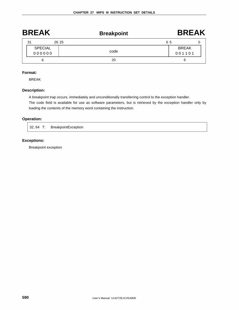
CHAPTER 27 MIPS III INSTRUCTION SET DETAILS
User’s Manual U14272EJ1V0UM00590
BREAK Breakpoint BREAK
SPECIAL
31 26 25 6 5 0
code0 0 0 0 0 0BREAK
0 0 1 1 0 1
6 20 6
Format:
BREAK
Description:
A breakpoint trap occurs, immediately and unconditionally transferring control to the exception handler.
The code field is available for use as software parameters, but is retrieved by the exception handler only by
loading the contents of the memory word containing the instruction.
Operation:
32, 64 T: BreakpointException
Exceptions:
Breakpoint exception
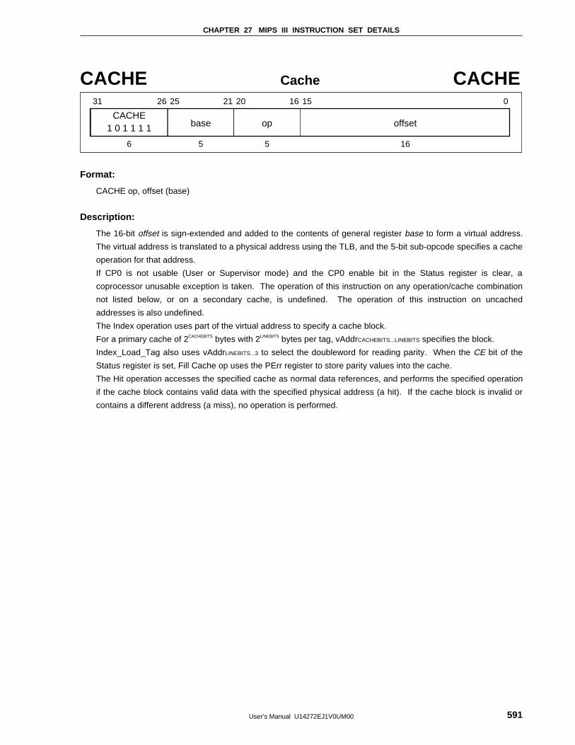
CHAPTER 27 MIPS III INSTRUCTION SET DETAILS
User’s Manual U14272EJ1V0UM00 591
CACHE Cache CACHE
CACHE
31 26 25 21 20 16 15 0
base1 0 1 1 1 1 op offset
6 5 5 16
Format:
CACHE op, offset (base)
Description:
The 16-bit offset is sign-extended and added to the contents of general register base to form a virtual address.
The virtual address is translated to a physical address using the TLB, and the 5-bit sub-opcode specifies a cache
operation for that address.
If CP0 is not usable (User or Supervisor mode) and the CP0 enable bit in the Status register is clear, a
coprocessor unusable exception is taken. The operation of this instruction on any operation/cache combination
not listed below, or on a secondary cache, is undefined. The operation of this instruction on uncached
addresses is also undefined.
The Index operation uses part of the virtual address to specify a cache block.
For a primary cache of 2CACHEBITS bytes with 2LINEBITS bytes per tag, vAddrCACHEBITS...LINEBITS specifies the block.
Index_Load_Tag also uses vAddrLINEBITS...3 to select the doubleword for reading parity. When the CE bit of the
Status register is set, Fill Cache op uses the PErr register to store parity values into the cache.
The Hit operation accesses the specified cache as normal data references, and performs the specified operation
if the cache block contains valid data with the specified physical address (a hit). If the cache block is invalid or
contains a different address (a miss), no operation is performed.
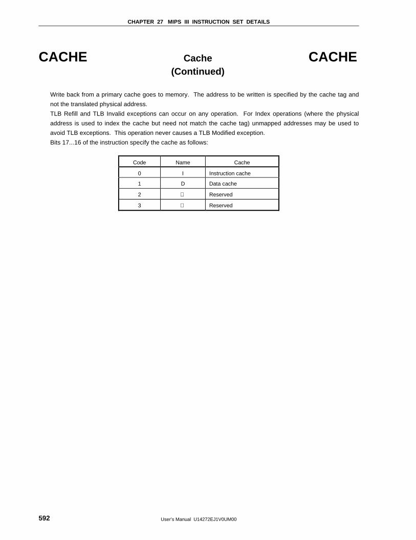
CHAPTER 27 MIPS III INSTRUCTION SET DETAILS
User’s Manual U14272EJ1V0UM00592
CACHE Cache CACHE(Continued)
Write back from a primary cache goes to memory. The address to be written is specified by the cache tag and
not the translated physical address.
TLB Refill and TLB Invalid exceptions can occur on any operation. For Index operations (where the physical
address is used to index the cache but need not match the cache tag) unmapped addresses may be used to
avoid TLB exceptions. This operation never causes a TLB Modified exception.
Bits 17...16 of the instruction specify the cache as follows:
Code Name Cache
0 I Instruction cache
1 D Data cache
2 Reserved
3 Reserved
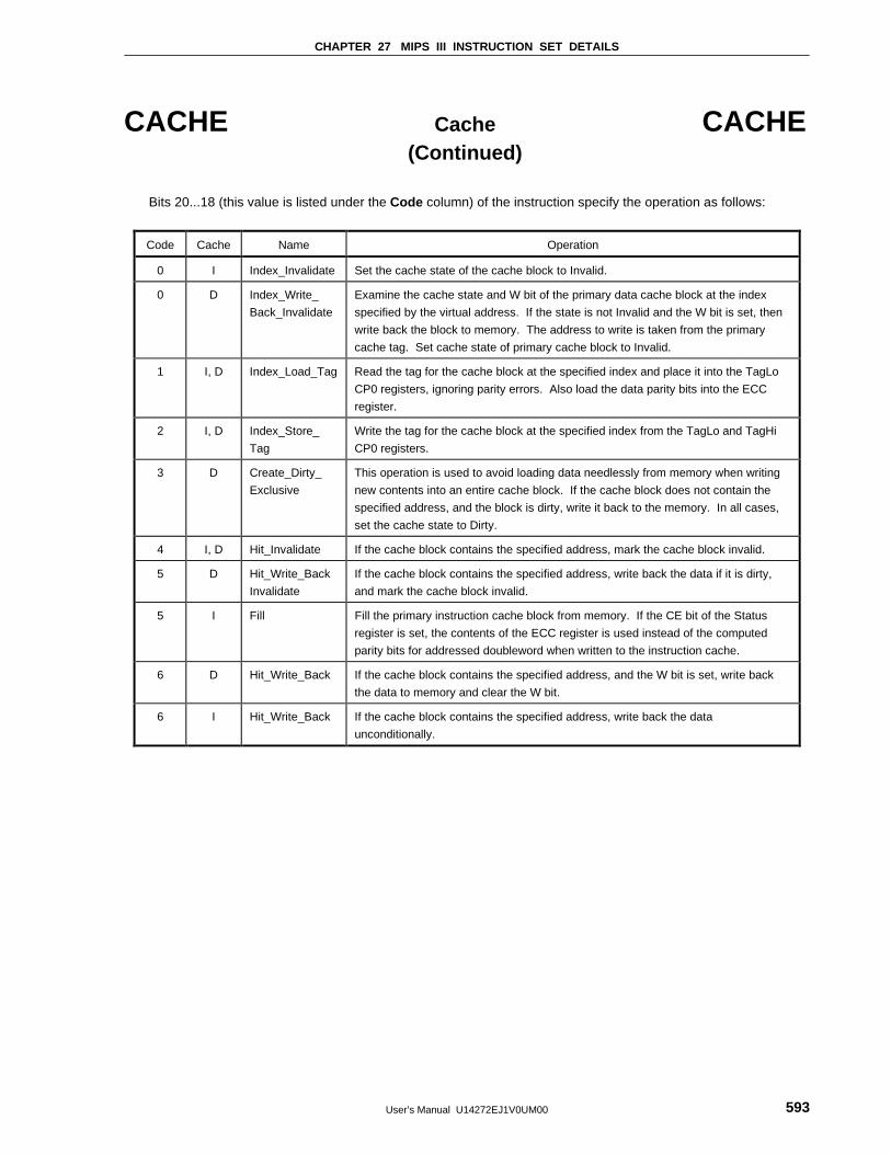
CHAPTER 27 MIPS III INSTRUCTION SET DETAILS
User’s Manual U14272EJ1V0UM00 593
CACHE Cache CACHE(Continued)
Bits 20...18 (this value is listed under the Code column) of the instruction specify the operation as follows:
Code Cache Name Operation
0 I Index_Invalidate Set the cache state of the cache block to Invalid.
0 D Index_Write_
Back_Invalidate
Examine the cache state and W bit of the primary data cache block at the index
specified by the virtual address. If the state is not Invalid and the W bit is set, then
write back the block to memory. The address to write is taken from the primary
cache tag. Set cache state of primary cache block to Invalid.
1 I, D Index_Load_Tag Read the tag for the cache block at the specified index and place it into the TagLo
CP0 registers, ignoring parity errors. Also load the data parity bits into the ECC
register.
2 I, D Index_Store_
Tag
Write the tag for the cache block at the specified index from the TagLo and TagHi
CP0 registers.
3 D Create_Dirty_
Exclusive
This operation is used to avoid loading data needlessly from memory when writing
new contents into an entire cache block. If the cache block does not contain the
specified address, and the block is dirty, write it back to the memory. In all cases,
set the cache state to Dirty.
4 I, D Hit_Invalidate If the cache block contains the specified address, mark the cache block invalid.
5 D Hit_Write_Back
Invalidate
If the cache block contains the specified address, write back the data if it is dirty,
and mark the cache block invalid.
5 I Fill Fill the primary instruction cache block from memory. If the CE bit of the Status
register is set, the contents of the ECC register is used instead of the computed
parity bits for addressed doubleword when written to the instruction cache.
6 D Hit_Write_Back If the cache block contains the specified address, and the W bit is set, write back
the data to memory and clear the W bit.
6 I Hit_Write_Back If the cache block contains the specified address, write back the data
unconditionally.
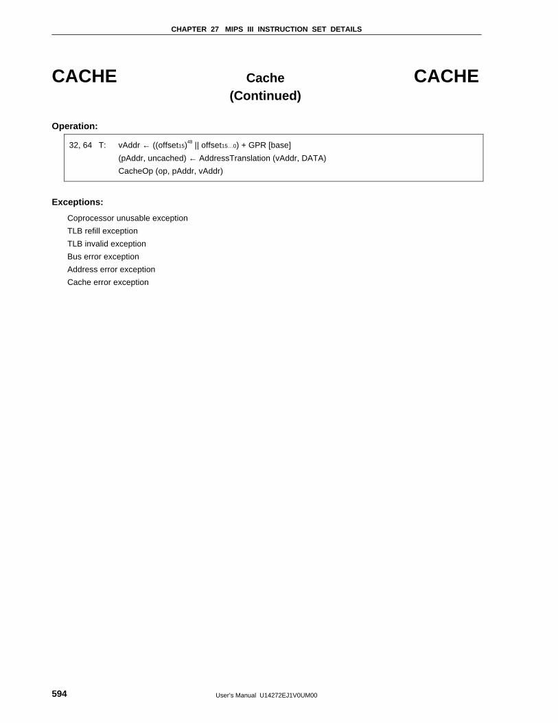
CHAPTER 27 MIPS III INSTRUCTION SET DETAILS
User’s Manual U14272EJ1V0UM00594
CACHE Cache CACHE(Continued)
Operation:
32, 64 T: vAddr ← ((offset15)48 || offset15…0) + GPR [base]
(pAddr, uncached) ← AddressTranslation (vAddr, DATA)
CacheOp (op, pAddr, vAddr)
Exceptions:
Coprocessor unusable exception
TLB refill exception
TLB invalid exception
Bus error exception
Address error exception
Cache error exception
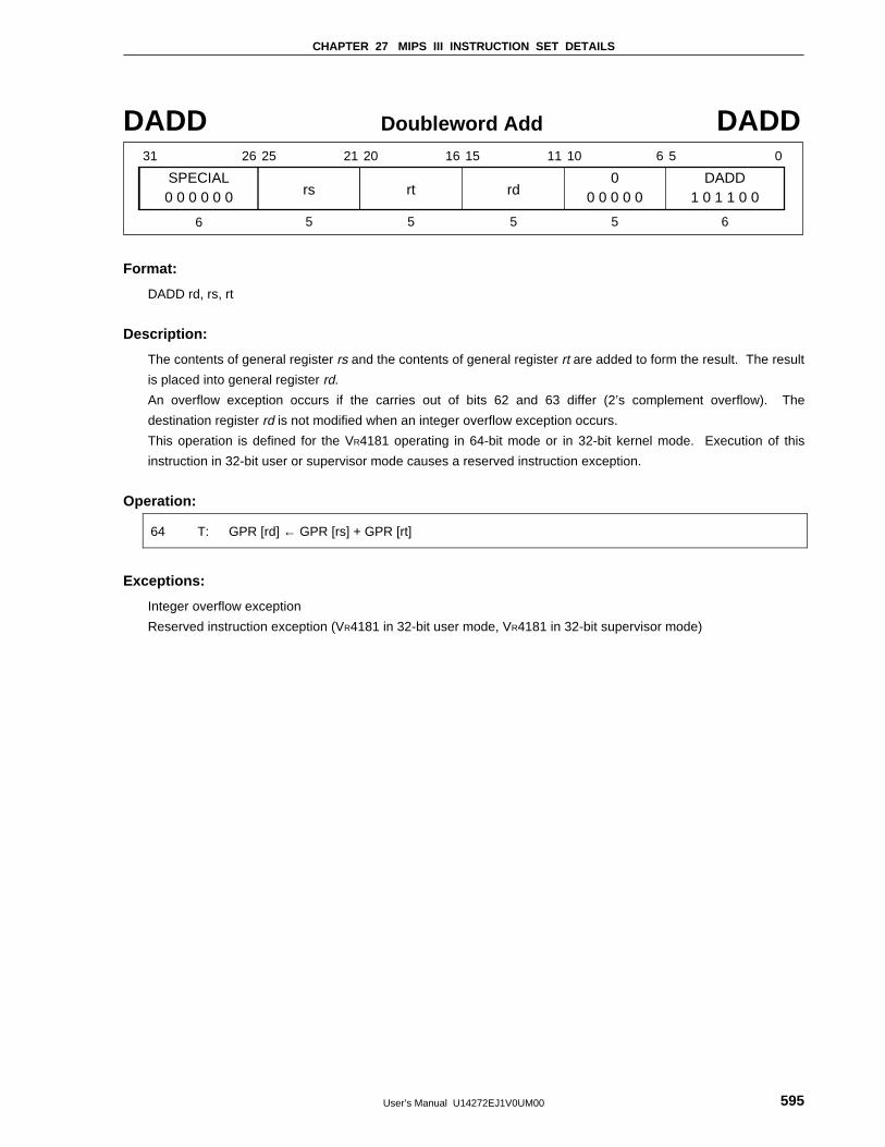
CHAPTER 27 MIPS III INSTRUCTION SET DETAILS
User’s Manual U14272EJ1V0UM00 595
DADD Doubleword Add DADD
SPECIAL
31 26 25 21 20 16 15 11 10 6 5 0
rs0 0 0 0 0 0 rt rd0
0 0 0 0 0DADD
1 0 1 1 0 0
6 5 5 5 5 6
Format:
DADD rd, rs, rt
Description:
The contents of general register rs and the contents of general register rt are added to form the result. The result
is placed into general register rd.
An overflow exception occurs if the carries out of bits 62 and 63 differ (2’s complement overflow). The
destination register rd is not modified when an integer overflow exception occurs.
This operation is defined for the VR4181 operating in 64-bit mode or in 32-bit kernel mode. Execution of this
instruction in 32-bit user or supervisor mode causes a reserved instruction exception.
Operation:
64 T: GPR [rd] ← GPR [rs] + GPR [rt]
Exceptions:
Integer overflow exception
Reserved instruction exception (VR4181 in 32-bit user mode, VR4181 in 32-bit supervisor mode)
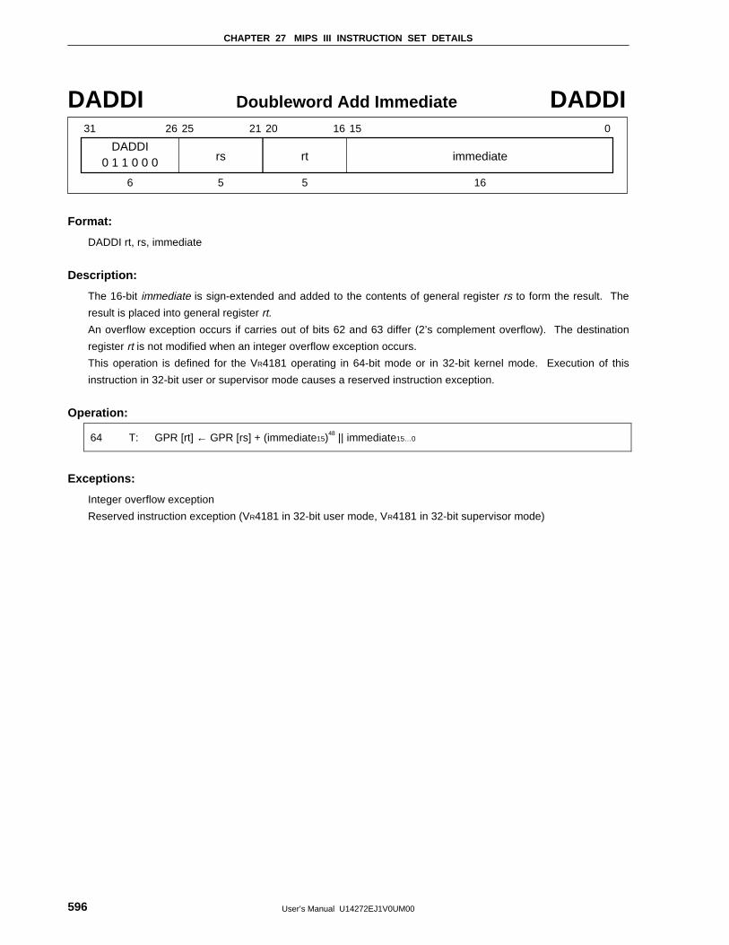
CHAPTER 27 MIPS III INSTRUCTION SET DETAILS
User’s Manual U14272EJ1V0UM00596
DADDI Doubleword Add Immediate DADDI
DADDI
31 26 25 21 20 16 15 0
rs0 1 1 0 0 0 rt immediate
6 5 5 16
Format:
DADDI rt, rs, immediate
Description:
The 16-bit immediate is sign-extended and added to the contents of general register rs to form the result. The
result is placed into general register rt.
An overflow exception occurs if carries out of bits 62 and 63 differ (2’s complement overflow). The destination
register rt is not modified when an integer overflow exception occurs.
This operation is defined for the VR4181 operating in 64-bit mode or in 32-bit kernel mode. Execution of this
instruction in 32-bit user or supervisor mode causes a reserved instruction exception.
Operation:
64 T: GPR [rt] ← GPR [rs] + (immediate15)48 || immediate15…0
Exceptions:
Integer overflow exception
Reserved instruction exception (VR4181 in 32-bit user mode, VR4181 in 32-bit supervisor mode)
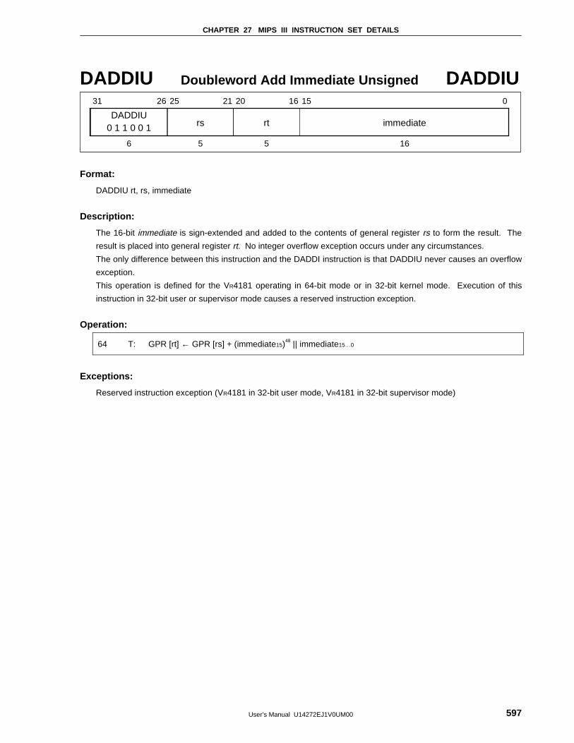
CHAPTER 27 MIPS III INSTRUCTION SET DETAILS
User’s Manual U14272EJ1V0UM00 597
DADDIU Doubleword Add Immediate Unsigned DADDIU
DADDIU
31 26 25 21 20 16 15 0
rs0 1 1 0 0 1 rt immediate
6 5 5 16
Format:
DADDIU rt, rs, immediate
Description:
The 16-bit immediate is sign-extended and added to the contents of general register rs to form the result. The
result is placed into general register rt. No integer overflow exception occurs under any circumstances.
The only difference between this instruction and the DADDI instruction is that DADDIU never causes an overflow
exception.
This operation is defined for the VR4181 operating in 64-bit mode or in 32-bit kernel mode. Execution of this
instruction in 32-bit user or supervisor mode causes a reserved instruction exception.
Operation:
64 T: GPR [rt] ← GPR [rs] + (immediate15)48 || immediate15…0
Exceptions:
Reserved instruction exception (VR4181 in 32-bit user mode, VR4181 in 32-bit supervisor mode)
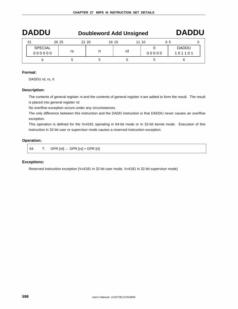
CHAPTER 27 MIPS III INSTRUCTION SET DETAILS
User’s Manual U14272EJ1V0UM00598
DADDU Doubleword Add Unsigned DADDU
SPECIAL
31 26 25 21 20 16 15 11 10 6 5 0
rs0 0 0 0 0 0 rt rd0
0 0 0 0 0DADDU
1 0 1 1 0 1
6 5 5 5 5 6
Format:
DADDU rd, rs, rt
Description:
The contents of general register rs and the contents of general register rt are added to form the result. The result
is placed into general register rd.
No overflow exception occurs under any circumstances.
The only difference between this instruction and the DADD instruction is that DADDU never causes an overflow
exception.
This operation is defined for the VR4181 operating in 64-bit mode or in 32-bit kernel mode. Execution of this
instruction in 32-bit user or supervisor mode causes a reserved instruction exception.
Operation:
64 T: GPR [rd] ← GPR [rs] + GPR [rt]
Exceptions:
Reserved instruction exception (VR4181 in 32-bit user mode, VR4181 in 32-bit supervisor mode)
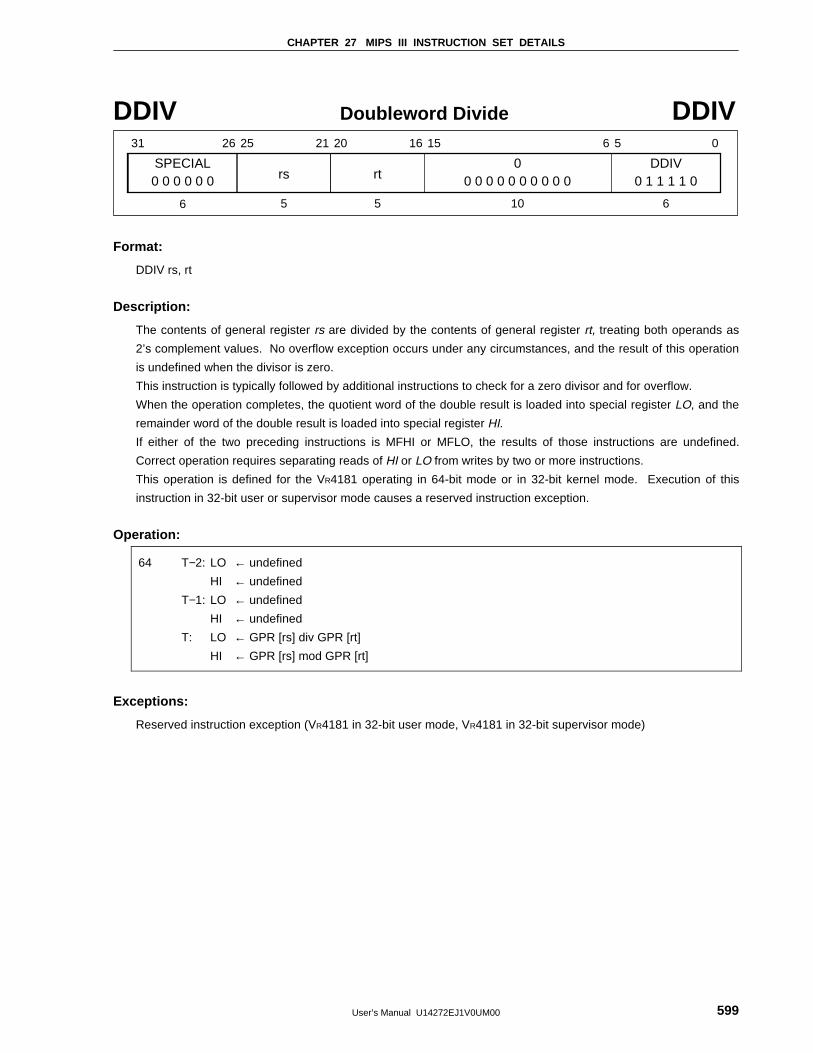
CHAPTER 27 MIPS III INSTRUCTION SET DETAILS
User’s Manual U14272EJ1V0UM00 599
DDIV Doubleword Divide DDIV
SPECIAL
31 26 25 21 20 16 15 6 5 0
rs0 0 0 0 0 0 rt0
0 0 0 0 0 0 0 0 0 0DDIV
0 1 1 1 1 0
6 5 5 10 6
Format:
DDIV rs, rt
Description:
The contents of general register rs are divided by the contents of general register rt, treating both operands as
2’s complement values. No overflow exception occurs under any circumstances, and the result of this operation
is undefined when the divisor is zero.
This instruction is typically followed by additional instructions to check for a zero divisor and for overflow.
When the operation completes, the quotient word of the double result is loaded into special register LO, and the
remainder word of the double result is loaded into special register HI.
If either of the two preceding instructions is MFHI or MFLO, the results of those instructions are undefined.
Correct operation requires separating reads of HI or LO from writes by two or more instructions.
This operation is defined for the VR4181 operating in 64-bit mode or in 32-bit kernel mode. Execution of this
instruction in 32-bit user or supervisor mode causes a reserved instruction exception.
Operation:
64 T−2: LO ← undefined
HI ← undefined
T−1: LO ← undefined
HI ← undefined
T: LO ← GPR [rs] div GPR [rt]
HI ← GPR [rs] mod GPR [rt]
Exceptions:
Reserved instruction exception (VR4181 in 32-bit user mode, VR4181 in 32-bit supervisor mode)
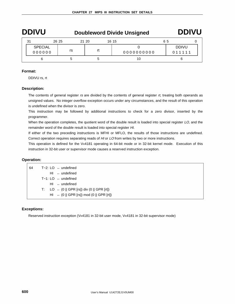
CHAPTER 27 MIPS III INSTRUCTION SET DETAILS
User’s Manual U14272EJ1V0UM00600
DDIVU Doubleword Divide Unsigned DDIVU
SPECIAL
31 26 25 21 20 16 15 6 5 0
rs0 0 0 0 0 0 rt0
0 0 0 0 0 0 0 0 0 0DDIVU
0 1 1 1 1 1
6 5 5 10 6
Format:
DDIVU rs, rt
Description:
The contents of general register rs are divided by the contents of general register rt, treating both operands as
unsigned values. No integer overflow exception occurs under any circumstances, and the result of this operation
is undefined when the divisor is zero.
This instruction may be followed by additional instructions to check for a zero divisor, inserted by the
programmer.
When the operation completes, the quotient word of the double result is loaded into special register LO, and the
remainder word of the double result is loaded into special register HI.
If either of the two preceding instructions is MFHI or MFLO, the results of those instructions are undefined.
Correct operation requires separating reads of HI or LO from writes by two or more instructions.
This operation is defined for the VR4181 operating in 64-bit mode or in 32-bit kernel mode. Execution of this
instruction in 32-bit user or supervisor mode causes a reserved instruction exception.
Operation:
64 T−2: LO ← undefined
HI ← undefined
T−1: LO ← undefined
HI ← undefined
T: LO ← (0 || GPR [rs]) div (0 || GPR [rt])
HI ← (0 || GPR [rs]) mod (0 || GPR [rt])
Exceptions:
Reserved instruction exception (VR4181 in 32-bit user mode, VR4181 in 32-bit supervisor mode)
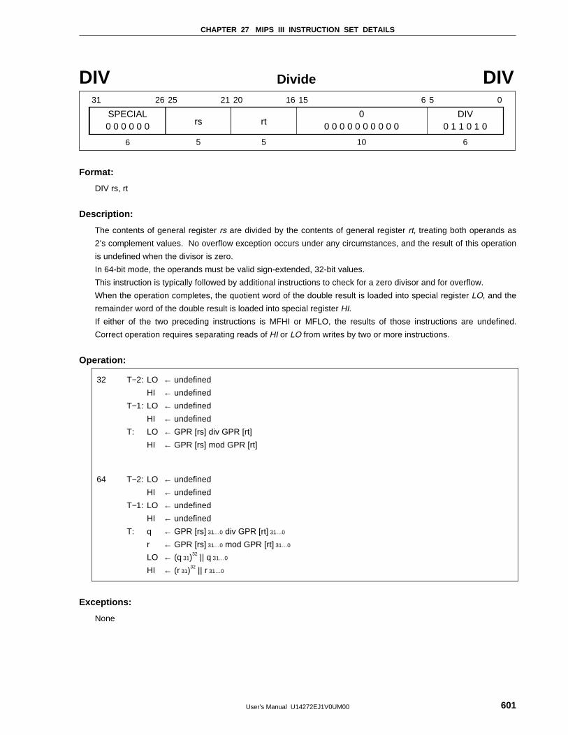
CHAPTER 27 MIPS III INSTRUCTION SET DETAILS
User’s Manual U14272EJ1V0UM00 601
DIV Divide DIV
SPECIAL
31 26 25 21 20 16 15 6 5 0
rs0 0 0 0 0 0 rt0
0 0 0 0 0 0 0 0 0 0DIV
0 1 1 0 1 0
6 5 5 10 6
Format:
DIV rs, rt
Description:
The contents of general register rs are divided by the contents of general register rt, treating both operands as
2’s complement values. No overflow exception occurs under any circumstances, and the result of this operation
is undefined when the divisor is zero.
In 64-bit mode, the operands must be valid sign-extended, 32-bit values.
This instruction is typically followed by additional instructions to check for a zero divisor and for overflow.
When the operation completes, the quotient word of the double result is loaded into special register LO, and the
remainder word of the double result is loaded into special register HI.
If either of the two preceding instructions is MFHI or MFLO, the results of those instructions are undefined.
Correct operation requires separating reads of HI or LO from writes by two or more instructions.
Operation:
32 T−2: LO ← undefined
HI ← undefined
T−1: LO ← undefined
HI ← undefined
T: LO ← GPR [rs] div GPR [rt]
HI ← GPR [rs] mod GPR [rt]
64 T−2: LO ← undefined
HI ← undefined
T−1: LO ← undefined
HI ← undefined
T: q ← GPR [rs] 31…0 div GPR [rt] 31…0
r ← GPR [rs] 31…0 mod GPR [rt] 31…0
LO ← (q 31)32 || q 31…0
HI ← (r 31)32 || r 31…0
Exceptions:
None
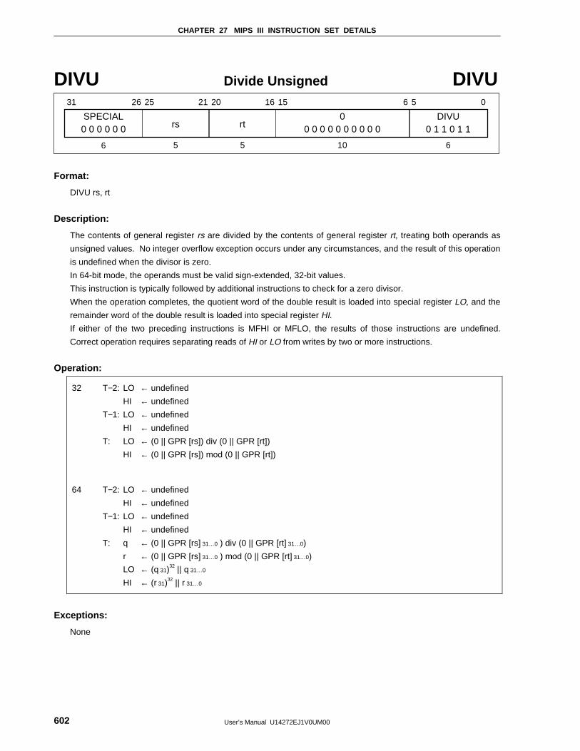
CHAPTER 27 MIPS III INSTRUCTION SET DETAILS
User’s Manual U14272EJ1V0UM00602
DIVU Divide Unsigned DIVU
SPECIAL
31 26 25 21 20 16 15 6 5 0
rs0 0 0 0 0 0 rt0
0 0 0 0 0 0 0 0 0 0DIVU
0 1 1 0 1 1
6 5 5 10 6
Format:
DIVU rs, rt
Description:
The contents of general register rs are divided by the contents of general register rt, treating both operands as
unsigned values. No integer overflow exception occurs under any circumstances, and the result of this operation
is undefined when the divisor is zero.
In 64-bit mode, the operands must be valid sign-extended, 32-bit values.
This instruction is typically followed by additional instructions to check for a zero divisor.
When the operation completes, the quotient word of the double result is loaded into special register LO, and the
remainder word of the double result is loaded into special register HI.
If either of the two preceding instructions is MFHI or MFLO, the results of those instructions are undefined.
Correct operation requires separating reads of HI or LO from writes by two or more instructions.
Operation:
32 T−2: LO ← undefined
HI ← undefined
T−1: LO ← undefined
HI ← undefined
T: LO ← (0 || GPR [rs]) div (0 || GPR [rt])
HI ← (0 || GPR [rs]) mod (0 || GPR [rt])
64 T−2: LO ← undefined
HI ← undefined
T−1: LO ← undefined
HI ← undefined
T: q ← (0 || GPR [rs] 31…0 ) div (0 || GPR [rt] 31…0)
r ← (0 || GPR [rs] 31…0 ) mod (0 || GPR [rt] 31…0)
LO ← (q 31)32 || q 31…0
HI ← (r 31)32 || r 31…0
Exceptions:
None
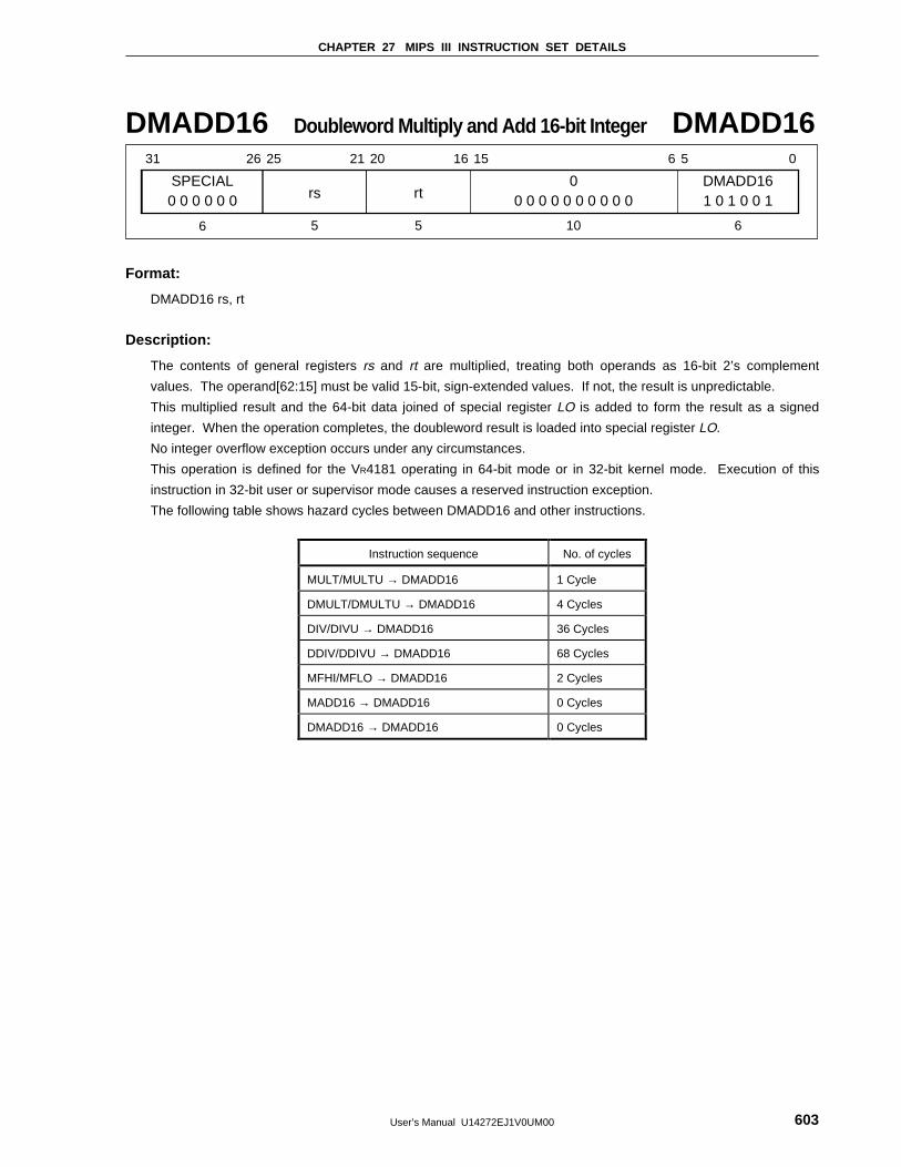
CHAPTER 27 MIPS III INSTRUCTION SET DETAILS
User’s Manual U14272EJ1V0UM00 603
DMADD16 Doubleword Multiply and Add 16-bit Integer DMADD16
SPECIAL
31 26 25 21 20 16 15 6 5 0
rs0 0 0 0 0 0 rt0
0 0 0 0 0 0 0 0 0 0DMADD161 0 1 0 0 1
6 5 5 10 6
Format:
DMADD16 rs, rt
Description:
The contents of general registers rs and rt are multiplied, treating both operands as 16-bit 2’s complement
values. The operand[62:15] must be valid 15-bit, sign-extended values. If not, the result is unpredictable.
This multiplied result and the 64-bit data joined of special register LO is added to form the result as a signed
integer. When the operation completes, the doubleword result is loaded into special register LO.
No integer overflow exception occurs under any circumstances.
This operation is defined for the VR4181 operating in 64-bit mode or in 32-bit kernel mode. Execution of this
instruction in 32-bit user or supervisor mode causes a reserved instruction exception.
The following table shows hazard cycles between DMADD16 and other instructions.
Instruction sequence No. of cycles
MULT/MULTU → DMADD16 1 Cycle
DMULT/DMULTU → DMADD16 4 Cycles
DIV/DIVU → DMADD16 36 Cycles
DDIV/DDIVU → DMADD16 68 Cycles
MFHI/MFLO → DMADD16 2 Cycles
MADD16 → DMADD16 0 Cycles
DMADD16 → DMADD16 0 Cycles
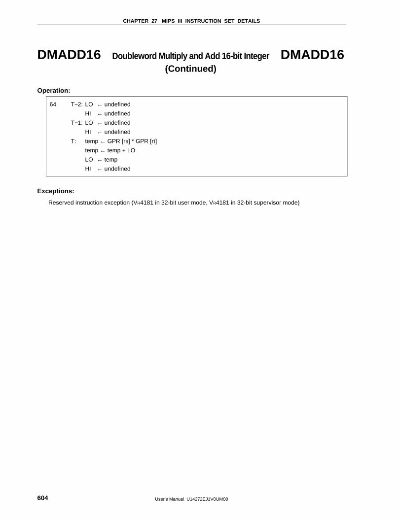
CHAPTER 27 MIPS III INSTRUCTION SET DETAILS
User’s Manual U14272EJ1V0UM00604
DMADD16 Doubleword Multiply and Add 16-bit Integer DMADD16(Continued)
Operation:
64 T−2: LO ← undefined
HI ← undefined
T−1: LO ← undefined
HI ← undefined
T: temp ← GPR [rs] * GPR [rt]
temp ← temp + LO
LO ← temp
HI ← undefined
Exceptions:
Reserved instruction exception (VR4181 in 32-bit user mode, VR4181 in 32-bit supervisor mode)
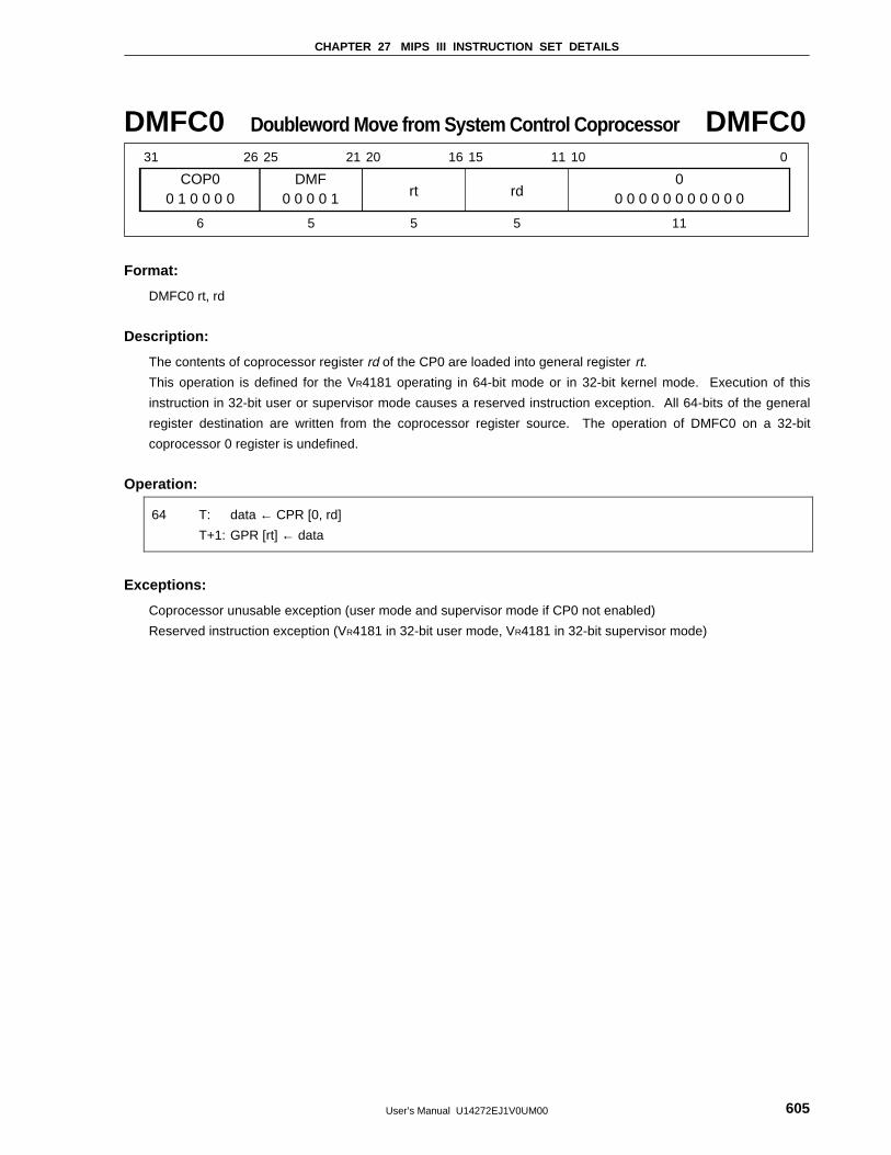
CHAPTER 27 MIPS III INSTRUCTION SET DETAILS
User’s Manual U14272EJ1V0UM00 605
DMFC0 Doubleword Move from System Control Coprocessor DMFC0
COP0
31 26 25 21 20 16 15 11 10 0
0 1 0 0 0 0 rt rdDMF
0 0 0 0 10
0 0 0 0 0 0 0 0 0 0 0
6 5 5 5 11
Format:
DMFC0 rt, rd
Description:
The contents of coprocessor register rd of the CP0 are loaded into general register rt.
This operation is defined for the VR4181 operating in 64-bit mode or in 32-bit kernel mode. Execution of this
instruction in 32-bit user or supervisor mode causes a reserved instruction exception. All 64-bits of the general
register destination are written from the coprocessor register source. The operation of DMFC0 on a 32-bit
coprocessor 0 register is undefined.
Operation:
64 T: data ← CPR [0, rd]
T+1: GPR [rt] ← data
Exceptions:
Coprocessor unusable exception (user mode and supervisor mode if CP0 not enabled)
Reserved instruction exception (VR4181 in 32-bit user mode, VR4181 in 32-bit supervisor mode)
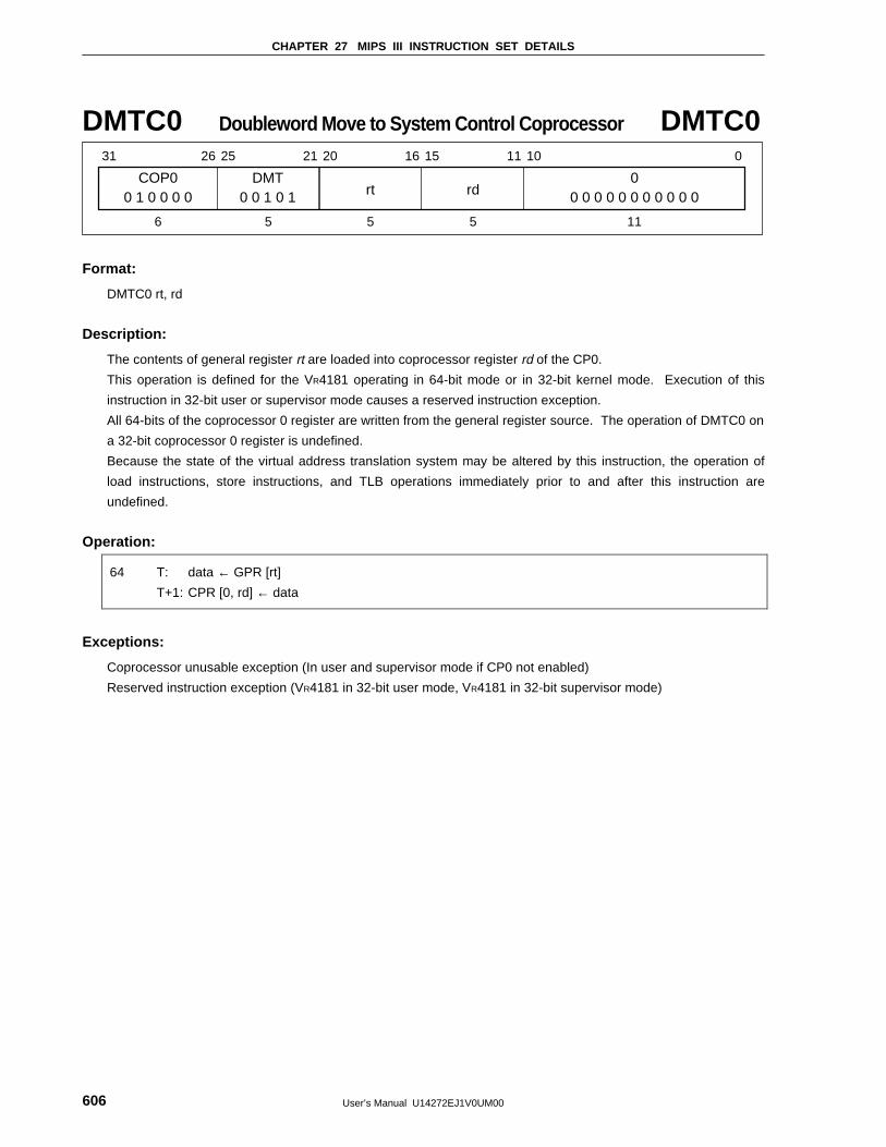
CHAPTER 27 MIPS III INSTRUCTION SET DETAILS
User’s Manual U14272EJ1V0UM00606
DMTC0 Doubleword Move to System Control Coprocessor DMTC0
COP0
31 26 25 21 20 16 15 11 10 0
0 1 0 0 0 0 rt rdDMT
0 0 1 0 10
0 0 0 0 0 0 0 0 0 0 0
6 5 5 5 11
Format:
DMTC0 rt, rd
Description:
The contents of general register rt are loaded into coprocessor register rd of the CP0.
This operation is defined for the VR4181 operating in 64-bit mode or in 32-bit kernel mode. Execution of this
instruction in 32-bit user or supervisor mode causes a reserved instruction exception.
All 64-bits of the coprocessor 0 register are written from the general register source. The operation of DMTC0 on
a 32-bit coprocessor 0 register is undefined.
Because the state of the virtual address translation system may be altered by this instruction, the operation of
load instructions, store instructions, and TLB operations immediately prior to and after this instruction are
undefined.
Operation:
64 T: data ← GPR [rt]
T+1: CPR [0, rd] ← data
Exceptions:
Coprocessor unusable exception (In user and supervisor mode if CP0 not enabled)
Reserved instruction exception (VR4181 in 32-bit user mode, VR4181 in 32-bit supervisor mode)
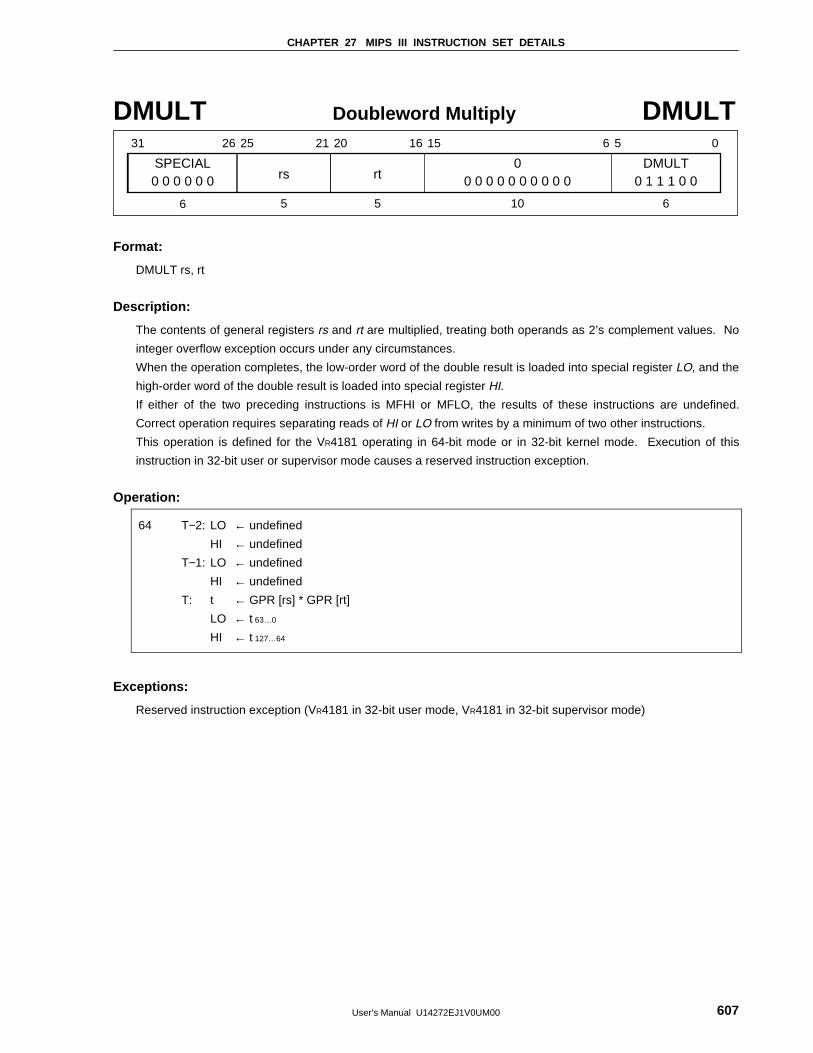
CHAPTER 27 MIPS III INSTRUCTION SET DETAILS
User’s Manual U14272EJ1V0UM00 607
DMULT Doubleword Multiply DMULT
SPECIAL
31 26 25 21 20 16 15 6 5 0
rs0 0 0 0 0 0 rt0
0 0 0 0 0 0 0 0 0 0DMULT
0 1 1 1 0 0
6 5 5 10 6
Format:
DMULT rs, rt
Description:
The contents of general registers rs and rt are multiplied, treating both operands as 2’s complement values. No
integer overflow exception occurs under any circumstances.
When the operation completes, the low-order word of the double result is loaded into special register LO, and the
high-order word of the double result is loaded into special register HI.
If either of the two preceding instructions is MFHI or MFLO, the results of these instructions are undefined.
Correct operation requires separating reads of HI or LO from writes by a minimum of two other instructions.
This operation is defined for the VR4181 operating in 64-bit mode or in 32-bit kernel mode. Execution of this
instruction in 32-bit user or supervisor mode causes a reserved instruction exception.
Operation:
64 T−2: LO ← undefined
HI ← undefined
T−1: LO ← undefined
HI ← undefined
T: t ← GPR [rs] * GPR [rt]
LO ← t 63…0
HI ← t 127…64
Exceptions:
Reserved instruction exception (VR4181 in 32-bit user mode, VR4181 in 32-bit supervisor mode)
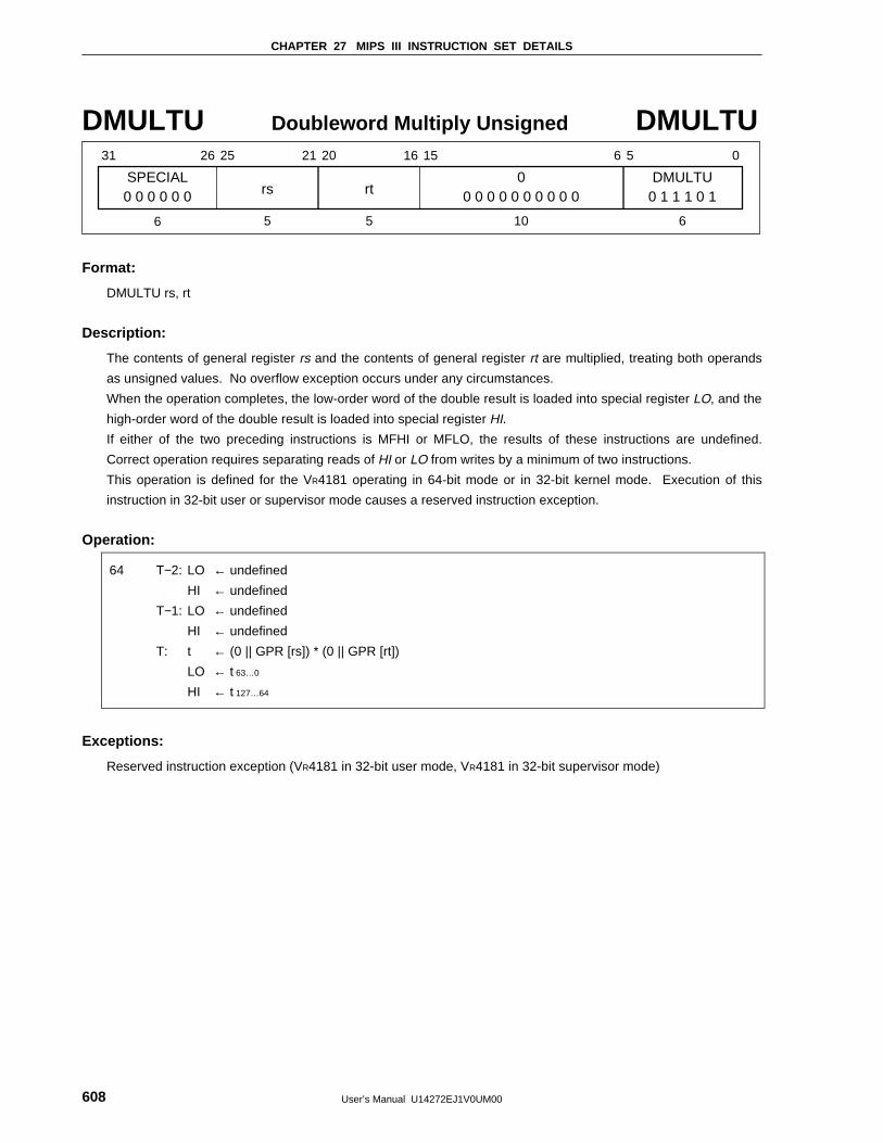
CHAPTER 27 MIPS III INSTRUCTION SET DETAILS
User’s Manual U14272EJ1V0UM00608
DMULTU Doubleword Multiply Unsigned DMULTU
SPECIAL
31 26 25 21 20 16 15 6 5 0
rs0 0 0 0 0 0 rt0
0 0 0 0 0 0 0 0 0 0DMULTU
0 1 1 1 0 1
6 5 5 10 6
Format:
DMULTU rs, rt
Description:
The contents of general register rs and the contents of general register rt are multiplied, treating both operands
as unsigned values. No overflow exception occurs under any circumstances.
When the operation completes, the low-order word of the double result is loaded into special register LO, and the
high-order word of the double result is loaded into special register HI.
If either of the two preceding instructions is MFHI or MFLO, the results of these instructions are undefined.
Correct operation requires separating reads of HI or LO from writes by a minimum of two instructions.
This operation is defined for the VR4181 operating in 64-bit mode or in 32-bit kernel mode. Execution of this
instruction in 32-bit user or supervisor mode causes a reserved instruction exception.
Operation:
64 T−2: LO ← undefined
HI ← undefined
T−1: LO ← undefined
HI ← undefined
T: t ← (0 || GPR [rs]) * (0 || GPR [rt])
LO ← t 63…0
HI ← t 127…64
Exceptions:
Reserved instruction exception (VR4181 in 32-bit user mode, VR4181 in 32-bit supervisor mode)
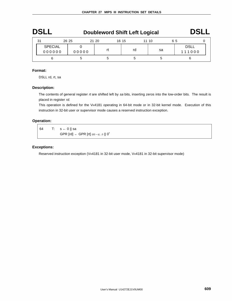
CHAPTER 27 MIPS III INSTRUCTION SET DETAILS
User’s Manual U14272EJ1V0UM00 609
DSLL Doubleword Shift Left Logical DSLL
SPECIAL
31 26 25 21 20 16 15 11 10 6 5 0
sa0 0 0 0 0 0 rt rd0
0 0 0 0 0DSLL
1 1 1 0 0 0
6 5 5 5 5 6
Format:
DSLL rd, rt, sa
Description:
The contents of general register rt are shifted left by sa bits, inserting zeros into the low-order bits. The result is
placed in register rd.
This operation is defined for the VR4181 operating in 64-bit mode or in 32-bit kernel mode. Execution of this
instruction in 32-bit user or supervisor mode causes a reserved instruction exception.
Operation:
64 T: s ← 0 || sa
GPR [rd] ← GPR [rt] (63 − s)…0 || 0s
Exceptions:
Reserved instruction exception (VR4181 in 32-bit user mode, VR4181 in 32-bit supervisor mode)
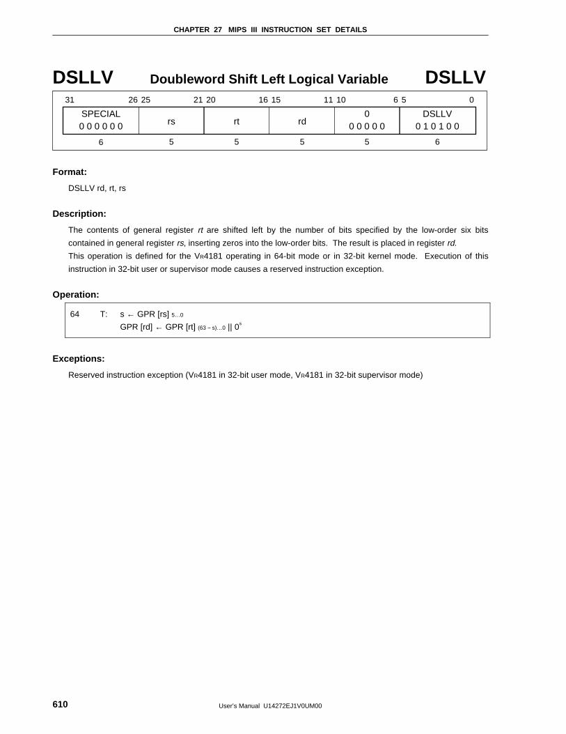
CHAPTER 27 MIPS III INSTRUCTION SET DETAILS
User’s Manual U14272EJ1V0UM00610
DSLLV Doubleword Shift Left Logical Variable DSLLV
SPECIAL
31 26 25 21 20 16 15 11 10 6 5 0
rs0 0 0 0 0 0 rt rd0
0 0 0 0 0DSLLV
0 1 0 1 0 0
6 5 5 5 5 6
Format:
DSLLV rd, rt, rs
Description:
The contents of general register rt are shifted left by the number of bits specified by the low-order six bits
contained in general register rs, inserting zeros into the low-order bits. The result is placed in register rd.
This operation is defined for the VR4181 operating in 64-bit mode or in 32-bit kernel mode. Execution of this
instruction in 32-bit user or supervisor mode causes a reserved instruction exception.
Operation:
64 T: s ← GPR [rs] 5…0
GPR [rd] ← GPR [rt] (63 − s)…0 || 0s
Exceptions:
Reserved instruction exception (VR4181 in 32-bit user mode, VR4181 in 32-bit supervisor mode)

CHAPTER 27 MIPS III INSTRUCTION SET DETAILS
User’s Manual U14272EJ1V0UM00 611
DSLL32 Doubleword Shift Left Logical + 32 DSLL32
SPECIAL
31 26 25 21 20 16 15 11 10 6 5 0
sa0 0 0 0 0 0 rt rd0
0 0 0 0 0DSLL32
1 1 1 1 0 0
6 5 5 5 5 6
Format:
DSLL32 rd, rt, sa
Description:
The contents of general register rt are shifted left by 32 + sa bits, inserting zeros into the low-order bits. The
result is placed in register rd.
This operation is defined for the VR4181 operating in 64-bit mode or in 32-bit kernel mode. Execution of this
instruction in 32-bit user or supervisor mode causes a reserved instruction exception.
Operation:
64 T: s ← 1 || sa
GPR [rd] ← GPR [rt] (63 − s)…0 || 0s
Exceptions:
Reserved instruction exception (VR4181 in 32-bit user mode, VR4181 in 32-bit supervisor mode)
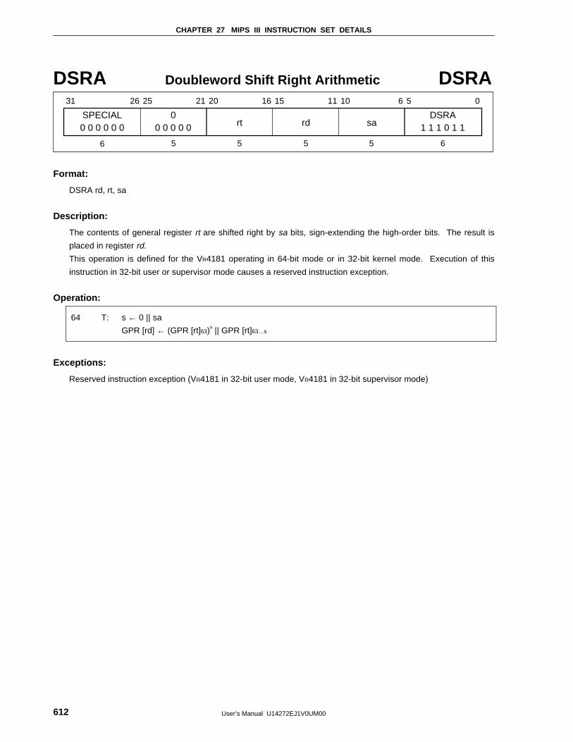
CHAPTER 27 MIPS III INSTRUCTION SET DETAILS
User’s Manual U14272EJ1V0UM00612
DSRA Doubleword Shift Right Arithmetic DSRA
SPECIAL
31 26 25 21 20 16 15 11 10 6 5 0
sa0 0 0 0 0 0 rt rd0
0 0 0 0 0DSRA
1 1 1 0 1 1
6 5 5 5 5 6
Format:
DSRA rd, rt, sa
Description:
The contents of general register rt are shifted right by sa bits, sign-extending the high-order bits. The result is
placed in register rd.
This operation is defined for the VR4181 operating in 64-bit mode or in 32-bit kernel mode. Execution of this
instruction in 32-bit user or supervisor mode causes a reserved instruction exception.
Operation:
64 T: s ← 0 || sa
GPR [rd] ← (GPR [rt]63)s || GPR [rt]63…s
Exceptions:
Reserved instruction exception (VR4181 in 32-bit user mode, VR4181 in 32-bit supervisor mode)
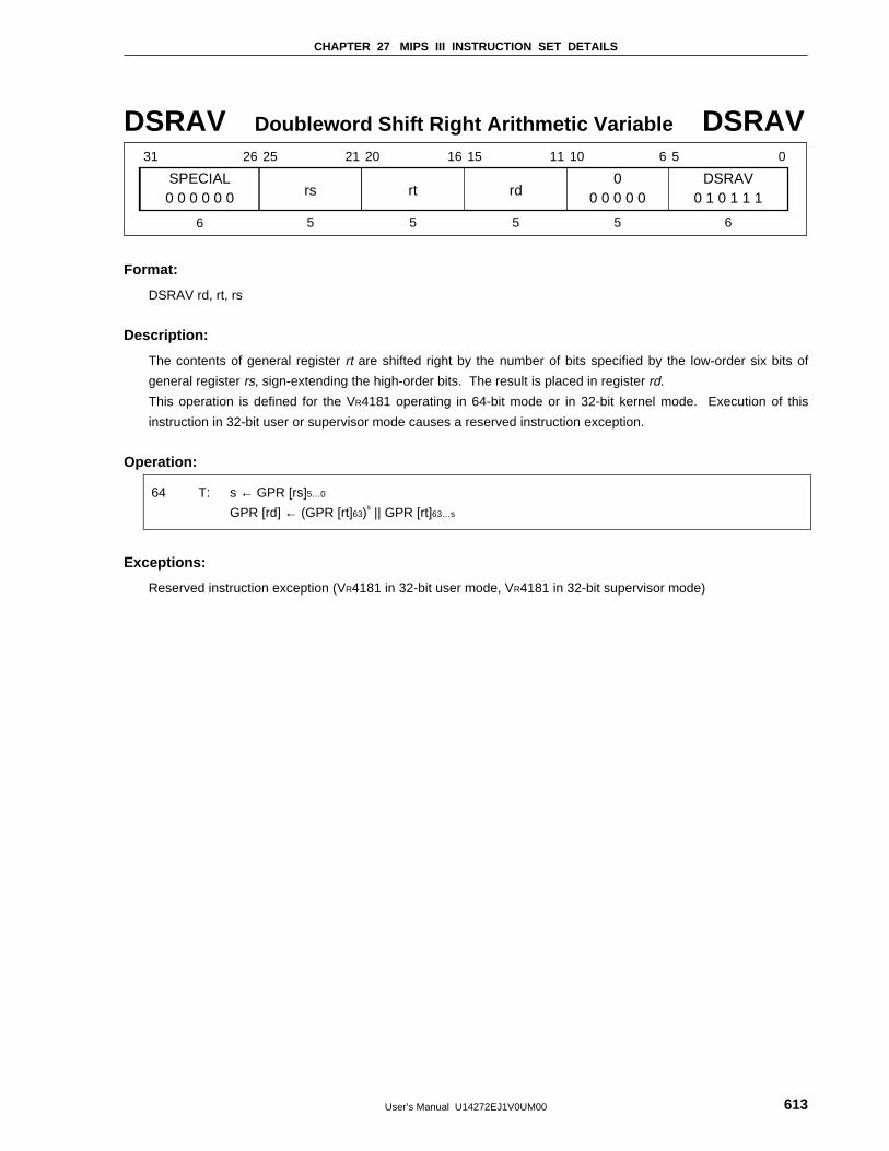
CHAPTER 27 MIPS III INSTRUCTION SET DETAILS
User’s Manual U14272EJ1V0UM00 613
DSRAV Doubleword Shift Right Arithmetic Variable DSRAV
SPECIAL
31 26 25 21 20 16 15 11 10 6 5 0
rs0 0 0 0 0 0 rt rd0
0 0 0 0 0DSRAV
0 1 0 1 1 1
6 5 5 5 5 6
Format:
DSRAV rd, rt, rs
Description:
The contents of general register rt are shifted right by the number of bits specified by the low-order six bits of
general register rs, sign-extending the high-order bits. The result is placed in register rd.
This operation is defined for the VR4181 operating in 64-bit mode or in 32-bit kernel mode. Execution of this
instruction in 32-bit user or supervisor mode causes a reserved instruction exception.
Operation:
64 T: s ← GPR [rs]5…0
GPR [rd] ← (GPR [rt]63)s || GPR [rt]63…s
Exceptions:
Reserved instruction exception (VR4181 in 32-bit user mode, VR4181 in 32-bit supervisor mode)

CHAPTER 27 MIPS III INSTRUCTION SET DETAILS
User’s Manual U14272EJ1V0UM00614
DSRA32 Doubleword Shift Right Arithmetic + 32 DSRA32
SPECIAL
31 26 25 21 20 16 15 11 10 6 5 0
sa0 0 0 0 0 0 rt rd0
0 0 0 0 0DSRA32
1 1 1 1 1 1
6 5 5 5 5 6
Format:
DSRA32 rd, rt, sa
Description:
The contents of general register rt are shifted right by 32 + sa bits, sign-extending the high-order bits. The result
is placed in register rd.
This operation is defined for the VR4181 operating in 64-bit mode or in 32-bit kernel mode. Execution of this
instruction in 32-bit user or supervisor mode causes a reserved instruction exception.
Operation:
64 T: s ← 1 || sa
GPR [rd] ← (GPR [rt]63)s || GPR [rt]63…s
Exceptions:
Reserved instruction exception (VR4181 in 32-bit user mode, VR4181 in 32-bit supervisor mode)
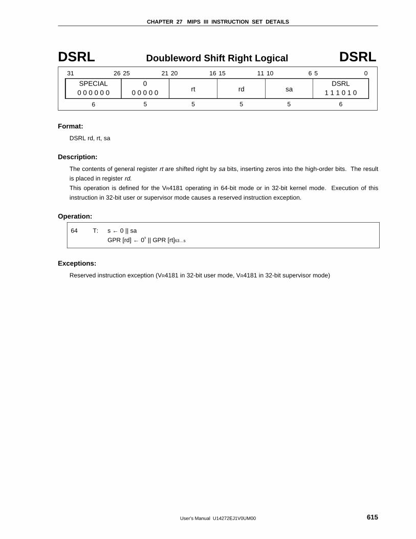
CHAPTER 27 MIPS III INSTRUCTION SET DETAILS
User’s Manual U14272EJ1V0UM00 615
DSRL Doubleword Shift Right Logical DSRL
SPECIAL
31 26 25 21 20 16 15 11 10 6 5 0
sa0 0 0 0 0 0 rt rd0
0 0 0 0 0DSRL
1 1 1 0 1 0
6 5 5 5 5 6
Format:
DSRL rd, rt, sa
Description:
The contents of general register rt are shifted right by sa bits, inserting zeros into the high-order bits. The result
is placed in register rd.
This operation is defined for the VR4181 operating in 64-bit mode or in 32-bit kernel mode. Execution of this
instruction in 32-bit user or supervisor mode causes a reserved instruction exception.
Operation:
64 T: s ← 0 || sa
GPR [rd] ← 0s || GPR [rt]63…s
Exceptions:
Reserved instruction exception (VR4181 in 32-bit user mode, VR4181 in 32-bit supervisor mode)
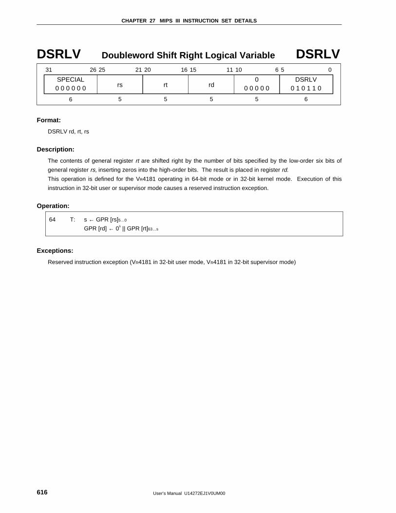
CHAPTER 27 MIPS III INSTRUCTION SET DETAILS
User’s Manual U14272EJ1V0UM00616
DSRLV Doubleword Shift Right Logical Variable DSRLV
SPECIAL
31 26 25 21 20 16 15 11 10 6 5 0
rs0 0 0 0 0 0 rt rd0
0 0 0 0 0DSRLV
0 1 0 1 1 0
6 5 5 5 5 6
Format:
DSRLV rd, rt, rs
Description:
The contents of general register rt are shifted right by the number of bits specified by the low-order six bits of
general register rs, inserting zeros into the high-order bits. The result is placed in register rd.
This operation is defined for the VR4181 operating in 64-bit mode or in 32-bit kernel mode. Execution of this
instruction in 32-bit user or supervisor mode causes a reserved instruction exception.
Operation:
64 T: s ← GPR [rs]5…0
GPR [rd] ← 0s || GPR [rt]63…s
Exceptions:
Reserved instruction exception (VR4181 in 32-bit user mode, VR4181 in 32-bit supervisor mode)
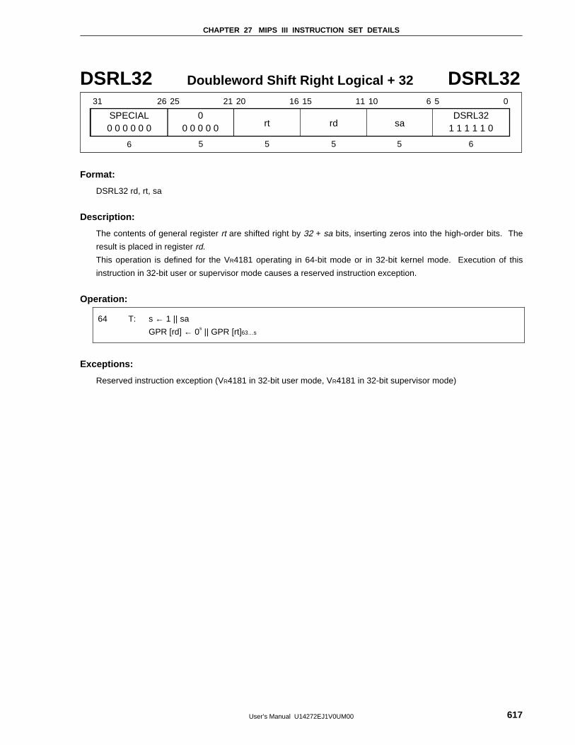
CHAPTER 27 MIPS III INSTRUCTION SET DETAILS
User’s Manual U14272EJ1V0UM00 617
DSRL32 Doubleword Shift Right Logical + 32 DSRL32
SPECIAL
31 26 25 21 20 16 15 11 10 6 5 0
sa0 0 0 0 0 0 rt rd0
0 0 0 0 0DSRL32
1 1 1 1 1 0
6 5 5 5 5 6
Format:
DSRL32 rd, rt, sa
Description:
The contents of general register rt are shifted right by 32 + sa bits, inserting zeros into the high-order bits. The
result is placed in register rd.
This operation is defined for the VR4181 operating in 64-bit mode or in 32-bit kernel mode. Execution of this
instruction in 32-bit user or supervisor mode causes a reserved instruction exception.
Operation:
64 T: s ← 1 || sa
GPR [rd] ← 0s || GPR [rt]63…s
Exceptions:
Reserved instruction exception (VR4181 in 32-bit user mode, VR4181 in 32-bit supervisor mode)
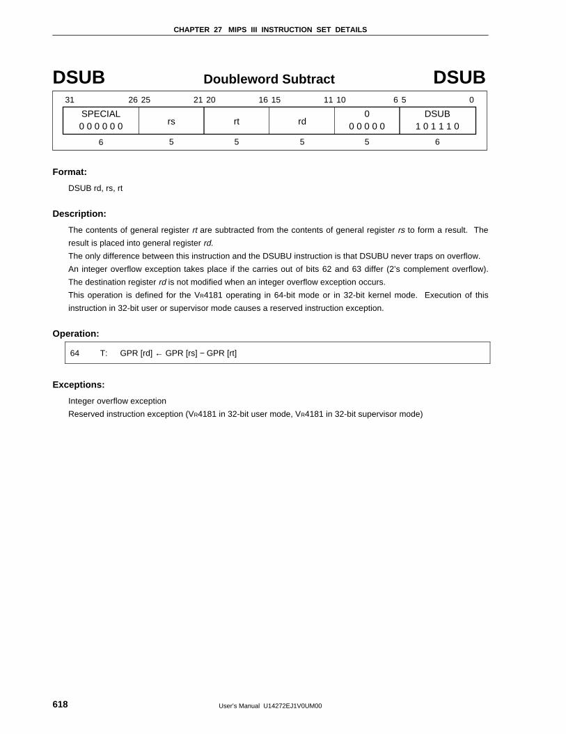
CHAPTER 27 MIPS III INSTRUCTION SET DETAILS
User’s Manual U14272EJ1V0UM00618
DSUB Doubleword Subtract DSUB
SPECIAL
31 26 25 21 20 16 15 11 10 6 5 0
rs0 0 0 0 0 0 rt rd0
0 0 0 0 0DSUB
1 0 1 1 1 0
6 5 5 5 5 6
Format:
DSUB rd, rs, rt
Description:
The contents of general register rt are subtracted from the contents of general register rs to form a result. The
result is placed into general register rd.
The only difference between this instruction and the DSUBU instruction is that DSUBU never traps on overflow.
An integer overflow exception takes place if the carries out of bits 62 and 63 differ (2’s complement overflow).
The destination register rd is not modified when an integer overflow exception occurs.
This operation is defined for the VR4181 operating in 64-bit mode or in 32-bit kernel mode. Execution of this
instruction in 32-bit user or supervisor mode causes a reserved instruction exception.
Operation:
64 T: GPR [rd] ← GPR [rs] − GPR [rt]
Exceptions:
Integer overflow exception
Reserved instruction exception (VR4181 in 32-bit user mode, VR4181 in 32-bit supervisor mode)
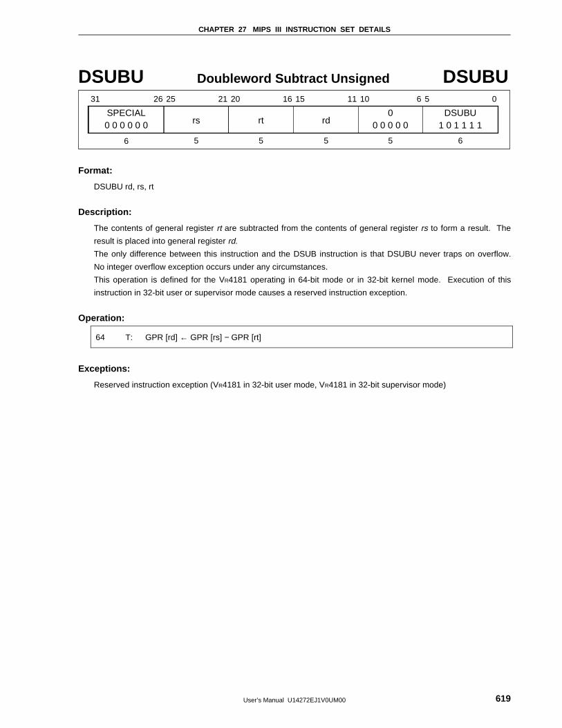
CHAPTER 27 MIPS III INSTRUCTION SET DETAILS
User’s Manual U14272EJ1V0UM00 619
DSUBU Doubleword Subtract Unsigned DSUBU
SPECIAL
31 26 25 21 20 16 15 11 10 6 5 0
rs0 0 0 0 0 0 rt rd0
0 0 0 0 0DSUBU
1 0 1 1 1 1
6 5 5 5 5 6
Format:
DSUBU rd, rs, rt
Description:
The contents of general register rt are subtracted from the contents of general register rs to form a result. The
result is placed into general register rd.
The only difference between this instruction and the DSUB instruction is that DSUBU never traps on overflow.
No integer overflow exception occurs under any circumstances.
This operation is defined for the VR4181 operating in 64-bit mode or in 32-bit kernel mode. Execution of this
instruction in 32-bit user or supervisor mode causes a reserved instruction exception.
Operation:
64 T: GPR [rd] ← GPR [rs] − GPR [rt]
Exceptions:
Reserved instruction exception (VR4181 in 32-bit user mode, VR4181 in 32-bit supervisor mode)
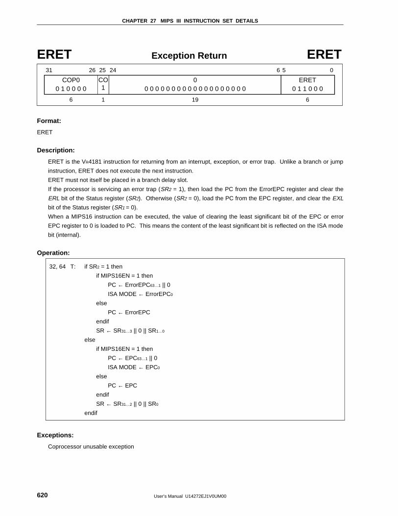
CHAPTER 27 MIPS III INSTRUCTION SET DETAILS
User’s Manual U14272EJ1V0UM00620
ERET Exception Return ERET
COP0
31 26 25 24 6 5 0
CO10 1 0 0 0 0
00 0 0 0 0 0 0 0 0 0 0 0 0 0 0 0 0 0 0
ERET0 1 1 0 0 0
6 1 19 6
Format:
ERET
Description:
ERET is the VR4181 instruction for returning from an interrupt, exception, or error trap. Unlike a branch or jump
instruction, ERET does not execute the next instruction.
ERET must not itself be placed in a branch delay slot.
If the processor is servicing an error trap (SR2 = 1), then load the PC from the ErrorEPC register and clear the
ERL bit of the Status register (SR2). Otherwise (SR2 = 0), load the PC from the EPC register, and clear the EXL
bit of the Status register (SR1 = 0).
When a MIPS16 instruction can be executed, the value of clearing the least significant bit of the EPC or error
EPC register to 0 is loaded to PC. This means the content of the least significant bit is reflected on the ISA mode
bit (internal).
Operation:
32, 64 T: if SR2 = 1 then
if MIPS16EN = 1 then
PC ← ErrorEPC63…1 || 0
ISA MODE ← ErrorEPC0
else
PC ← ErrorEPC
endif
SR ← SR31…3 || 0 || SR1…0
else
if MIPS16EN = 1 then
PC ← EPC63…1 || 0
ISA MODE ← EPC0
else
PC ← EPC
endif
SR ← SR31…2 || 0 || SR0
endif
Exceptions:
Coprocessor unusable exception
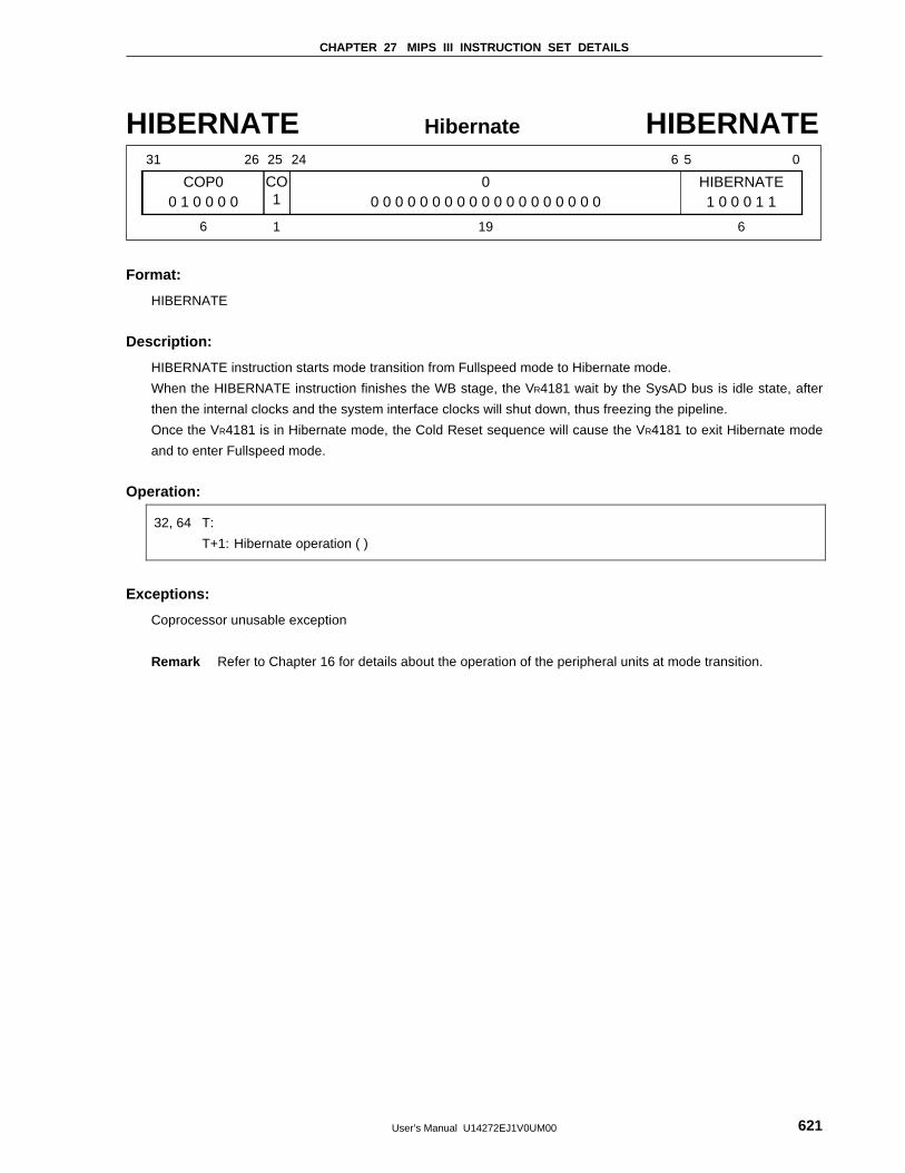
CHAPTER 27 MIPS III INSTRUCTION SET DETAILS
User’s Manual U14272EJ1V0UM00 621
HIBERNATE Hibernate HIBERNATE
COP0
31 26 25 24 6 5 0
CO10 1 0 0 0 0
00 0 0 0 0 0 0 0 0 0 0 0 0 0 0 0 0 0 0
HIBERNATE1 0 0 0 1 1
6 1 19 6
Format:
HIBERNATE
Description:
HIBERNATE instruction starts mode transition from Fullspeed mode to Hibernate mode.
When the HIBERNATE instruction finishes the WB stage, the VR4181 wait by the SysAD bus is idle state, after
then the internal clocks and the system interface clocks will shut down, thus freezing the pipeline.
Once the VR4181 is in Hibernate mode, the Cold Reset sequence will cause the VR4181 to exit Hibernate mode
and to enter Fullspeed mode.
Operation:
32, 64 T:
T+1: Hibernate operation ( )
Exceptions:
Coprocessor unusable exception
Remark Refer to Chapter 16 for details about the operation of the peripheral units at mode transition.
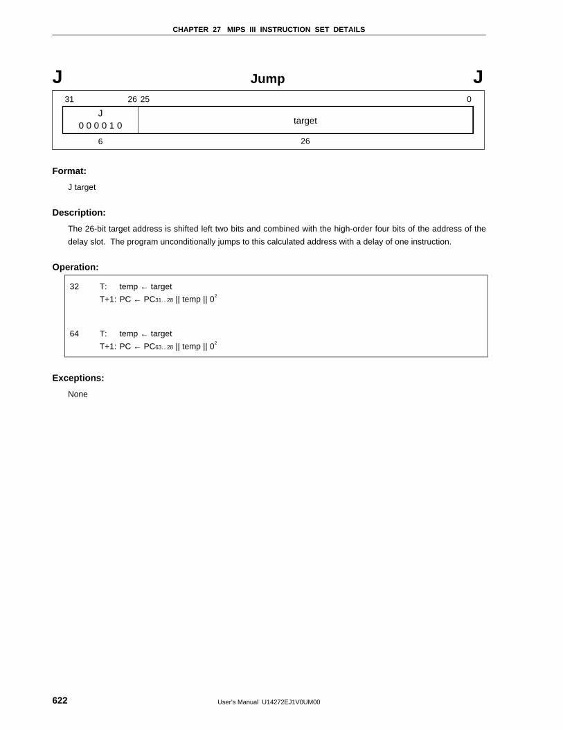
CHAPTER 27 MIPS III INSTRUCTION SET DETAILS
User’s Manual U14272EJ1V0UM00622
J Jump J
J
31 26 25 0
target0 0 0 0 1 0
6 26
Format:
J target
Description:
The 26-bit target address is shifted left two bits and combined with the high-order four bits of the address of the
delay slot. The program unconditionally jumps to this calculated address with a delay of one instruction.
Operation:
32 T: temp ← target
T+1: PC ← PC31…28 || temp || 02
64 T: temp ← target
T+1: PC ← PC63…28 || temp || 02
Exceptions:
None
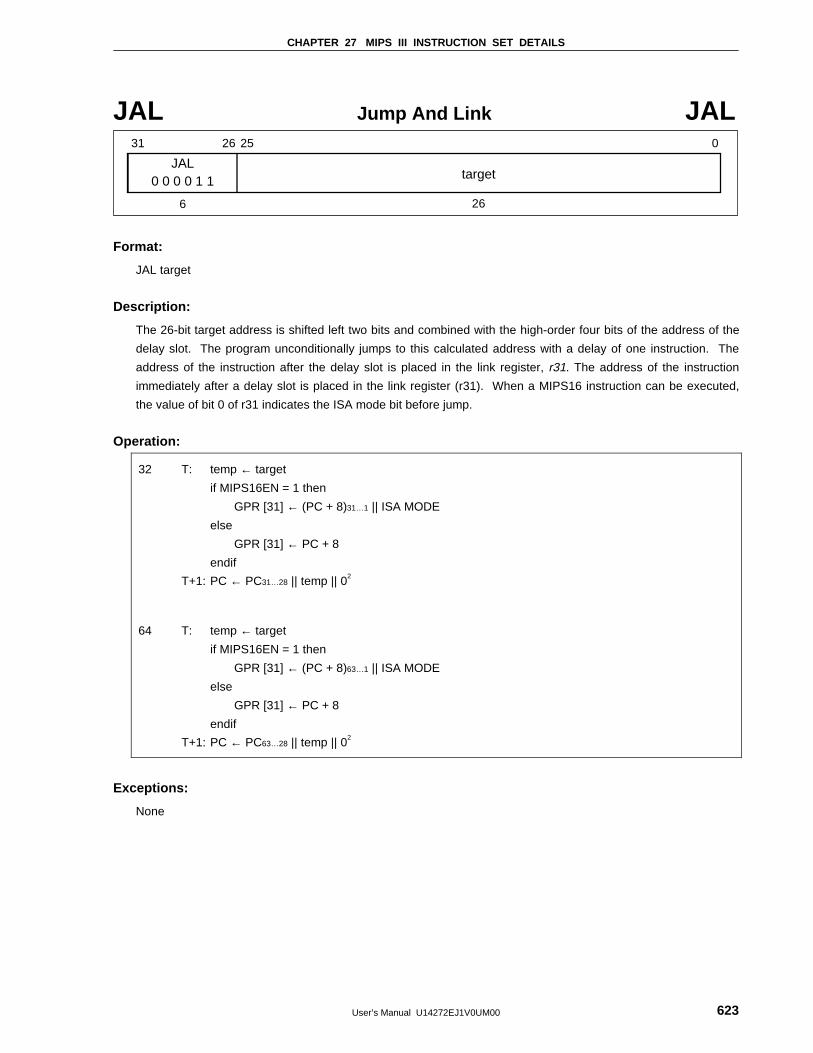
CHAPTER 27 MIPS III INSTRUCTION SET DETAILS
User’s Manual U14272EJ1V0UM00 623
JAL Jump And Link JAL
JAL
31 26 25 0
target0 0 0 0 1 1
6 26
Format:
JAL target
Description:
The 26-bit target address is shifted left two bits and combined with the high-order four bits of the address of the
delay slot. The program unconditionally jumps to this calculated address with a delay of one instruction. The
address of the instruction after the delay slot is placed in the link register, r31. The address of the instruction
immediately after a delay slot is placed in the link register (r31). When a MIPS16 instruction can be executed,
the value of bit 0 of r31 indicates the ISA mode bit before jump.
Operation:
32 T: temp ← target
if MIPS16EN = 1 then
GPR [31] ← (PC + 8)31…1 || ISA MODE
else
GPR [31] ← PC + 8
endif
T+1: PC ← PC31…28 || temp || 02
64 T: temp ← target
if MIPS16EN = 1 then
GPR [31] ← (PC + 8)63…1 || ISA MODE
else
GPR [31] ← PC + 8
endif
T+1: PC ← PC63…28 || temp || 02
Exceptions:
None
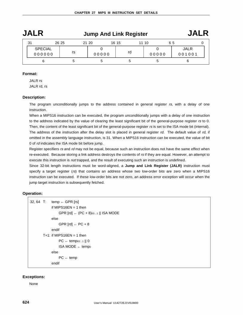
CHAPTER 27 MIPS III INSTRUCTION SET DETAILS
User’s Manual U14272EJ1V0UM00624
JALR Jump And Link Register JALR
SPECIAL
31 26 25 21 20 16 15 11 10 6 5 0
rs0 0 0 0 0 0 rd0
0 0 0 0 0JALR
0 0 1 0 0 1
6 5 5 5 5 6
00 0 0 0 0
Format:
JALR rs
JALR rd, rs
Description:
The program unconditionally jumps to the address contained in general register rs, with a delay of one
instruction.
When a MIPS16 instruction can be executed, the program unconditionally jumps with a delay of one instruction
to the address indicated by the value of clearing the least significant bit of the general-purpose register rs to 0.
Then, the content of the least significant bit of the general-purpose register rs is set to the ISA mode bit (internal).
The address of the instruction after the delay slot is placed in general register rd. The default value of rd, if
omitted in the assembly language instruction, is 31. When a MIPS16 instruction can be executed, the value of bit
0 of rd indicates the ISA mode bit before jump.
Register specifiers rs and rd may not be equal, because such an instruction does not have the same effect when
re-executed. Because storing a link address destroys the contents of rs if they are equal. However, an attempt to
execute this instruction is not trapped, and the result of executing such an instruction is undefined.
Since 32-bit length instructions must be word-aligned, a Jump and Link Register (JALR) instruction must
specify a target register (rs) that contains an address whose two low-order bits are zero when a MIPS16
instruction can be executed. If these low-order bits are not zero, an address error exception will occur when the
jump target instruction is subsequently fetched.
Operation:
32, 64 T: temp ← GPR [rs]
if MIPS16EN = 1 then
GPR [rd] ← (PC + 8)63…1 || ISA MODE
else
GPR [rd] ← PC + 8
endif
T+1: if MIPS16EN = 1 then
PC ← temp63…1 || 0
ISA MODE ← temp0
else
PC ← temp
endif
Exceptions:
None
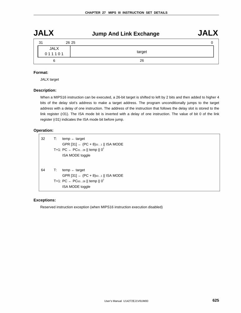
CHAPTER 27 MIPS III INSTRUCTION SET DETAILS
User’s Manual U14272EJ1V0UM00 625
JALX Jump And Link Exchange JALX
JALX
31 26 25 0
target0 1 1 1 0 1
6 26
Format:
JALX target
Description:
When a MIPS16 instruction can be executed, a 26-bit target is shifted to left by 2 bits and then added to higher 4
bits of the delay slot’s address to make a target address. The program unconditionally jumps to the target
address with a delay of one instruction. The address of the instruction that follows the delay slot is stored to the
link register (r31). The ISA mode bit is inverted with a delay of one instruction. The value of bit 0 of the link
register (r31) indicates the ISA mode bit before jump.
Operation:
32 T: temp ← target
GPR [31] ← (PC + 8)31…1 || ISA MODE
T+1: PC ← PC31…28 || temp || 02
ISA MODE toggle
64 T: temp ← target
GPR [31] ← (PC + 8)63…1 || ISA MODE
T+1: PC ← PC63…28 || temp || 02
ISA MODE toggle
Exceptions:
Reserved instruction exception (when MIPS16 instruction execution disabled)
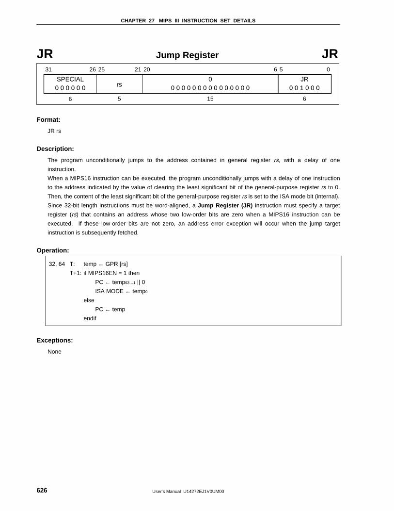
CHAPTER 27 MIPS III INSTRUCTION SET DETAILS
User’s Manual U14272EJ1V0UM00626
JR Jump Register JR
SPECIAL
31 26 25 21 20 6 5 0
rs0 0 0 0 0 00
0 0 0 0 0 0 0 0 0 0 0 0 0 0 0JR
0 0 1 0 0 0
6 5 15 6
Format:
JR rs
Description:
The program unconditionally jumps to the address contained in general register rs, with a delay of one
instruction.
When a MIPS16 instruction can be executed, the program unconditionally jumps with a delay of one instruction
to the address indicated by the value of clearing the least significant bit of the general-purpose register rs to 0.
Then, the content of the least significant bit of the general-purpose register rs is set to the ISA mode bit (internal).
Since 32-bit length instructions must be word-aligned, a Jump Register (JR) instruction must specify a target
register (rs) that contains an address whose two low-order bits are zero when a MIPS16 instruction can be
executed. If these low-order bits are not zero, an address error exception will occur when the jump target
instruction is subsequently fetched.
Operation:
32, 64 T: temp ← GPR [rs]
T+1: if MIPS16EN = 1 then
PC ← temp63…1 || 0
ISA MODE ← temp0
else
PC ← temp
endif
Exceptions:
None
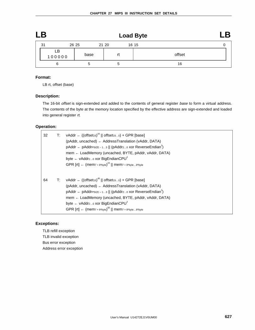
CHAPTER 27 MIPS III INSTRUCTION SET DETAILS
User’s Manual U14272EJ1V0UM00 627
LB Load Byte LB
LB
31 26 25 21 20 16 15 0
base1 0 0 0 0 0 rt offset
6 5 5 16
Format:
LB rt, offset (base)
Description:
The 16-bit offset is sign-extended and added to the contents of general register base to form a virtual address.
The contents of the byte at the memory location specified by the effective address are sign-extended and loaded
into general register rt.
Operation:
32 T: vAddr ← ((offset15)16 || offset15…0) + GPR [base]
(pAddr, uncached) ← AddressTranslation (vAddr, DATA)
pAddr ← pAddrPSIZE – 1…3 || (pAddr2…0 xor ReverseEndian3)
mem ← LoadMemory (uncached, BYTE, pAddr, vAddr, DATA)
byte ← vAddr2…0 xor BigEndianCPU3
GPR [rt] ← (mem7 + 8*byte)24 || mem7 + 8*byte…8*byte
64 T: vAddr ← ((offset15)48 || offset15…0) + GPR [base]
(pAddr, uncached) ← AddressTranslation (vAddr, DATA)
pAddr ← pAddrPSIZE – 1…3 || (pAddr2…0 xor ReverseEndian3)
mem ← LoadMemory (uncached, BYTE, pAddr, vAddr, DATA)
byte ← vAddr2…0 xor BigEndianCPU3
GPR [rt] ← (mem7 + 8*byte)56 || mem7 + 8*byte…8*byte
Exceptions:
TLB refill exception
TLB invalid exception
Bus error exception
Address error exception
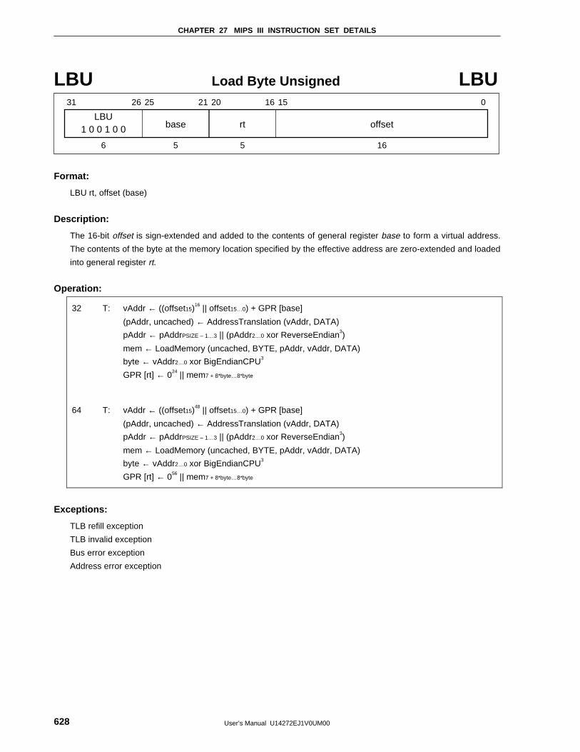
CHAPTER 27 MIPS III INSTRUCTION SET DETAILS
User’s Manual U14272EJ1V0UM00628
LBU Load Byte Unsigned LBU
LBU
31 26 25 21 20 16 15 0
base1 0 0 1 0 0 rt offset
6 5 5 16
Format:
LBU rt, offset (base)
Description:
The 16-bit offset is sign-extended and added to the contents of general register base to form a virtual address.
The contents of the byte at the memory location specified by the effective address are zero-extended and loaded
into general register rt.
Operation:
32 T: vAddr ← ((offset15)16 || offset15…0) + GPR [base]
(pAddr, uncached) ← AddressTranslation (vAddr, DATA)
pAddr ← pAddrPSIZE – 1…3 || (pAddr2…0 xor ReverseEndian3)
mem ← LoadMemory (uncached, BYTE, pAddr, vAddr, DATA)
byte ← vAddr2…0 xor BigEndianCPU3
GPR [rt] ← 024 || mem7 + 8*byte…8*byte
64 T: vAddr ← ((offset15)48 || offset15…0) + GPR [base]
(pAddr, uncached) ← AddressTranslation (vAddr, DATA)
pAddr ← pAddrPSIZE – 1…3 || (pAddr2…0 xor ReverseEndian3)
mem ← LoadMemory (uncached, BYTE, pAddr, vAddr, DATA)
byte ← vAddr2…0 xor BigEndianCPU3
GPR [rt] ← 056 || mem7 + 8*byte…8*byte
Exceptions:
TLB refill exception
TLB invalid exception
Bus error exception
Address error exception
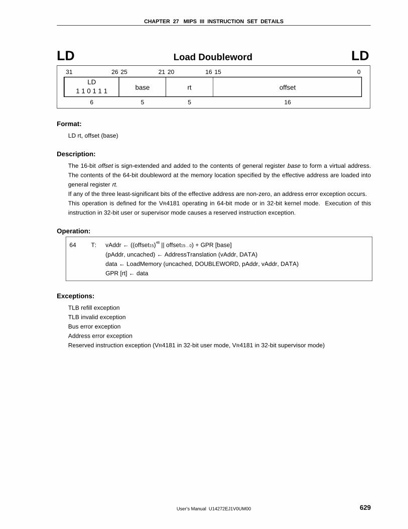
CHAPTER 27 MIPS III INSTRUCTION SET DETAILS
User’s Manual U14272EJ1V0UM00 629
LD Load Doubleword LD
LD
31 26 25 21 20 16 15 0
base1 1 0 1 1 1 rt offset
6 5 5 16
Format:
LD rt, offset (base)
Description:
The 16-bit offset is sign-extended and added to the contents of general register base to form a virtual address.
The contents of the 64-bit doubleword at the memory location specified by the effective address are loaded into
general register rt.
If any of the three least-significant bits of the effective address are non-zero, an address error exception occurs.
This operation is defined for the VR4181 operating in 64-bit mode or in 32-bit kernel mode. Execution of this
instruction in 32-bit user or supervisor mode causes a reserved instruction exception.
Operation:
64 T: vAddr ← ((offset15)48 || offset15…0) + GPR [base]
(pAddr, uncached) ← AddressTranslation (vAddr, DATA)
data ← LoadMemory (uncached, DOUBLEWORD, pAddr, vAddr, DATA)
GPR [rt] ← data
Exceptions:
TLB refill exception
TLB invalid exception
Bus error exception
Address error exception
Reserved instruction exception (VR4181 in 32-bit user mode, VR4181 in 32-bit supervisor mode)
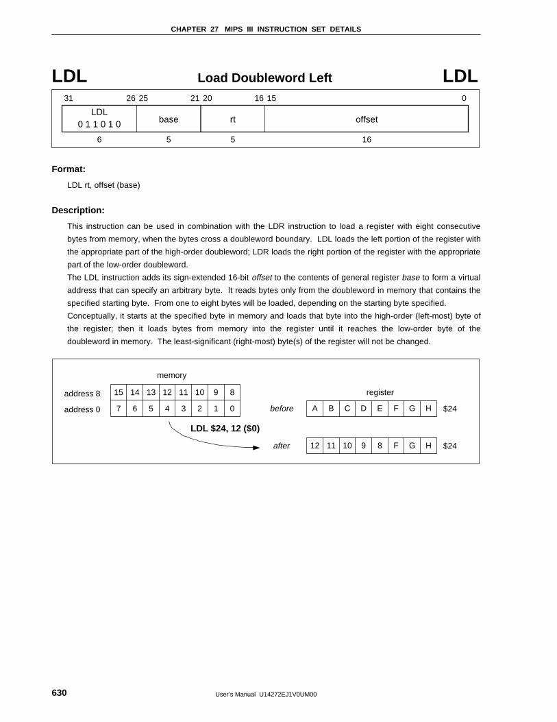
CHAPTER 27 MIPS III INSTRUCTION SET DETAILS
User’s Manual U14272EJ1V0UM00630
LDL Load Doubleword Left LDL
LDL
31 26 25 21 20 16 15 0
base0 1 1 0 1 0 rt offset
6 5 5 16
Format:
LDL rt, offset (base)
Description:
This instruction can be used in combination with the LDR instruction to load a register with eight consecutive
bytes from memory, when the bytes cross a doubleword boundary. LDL loads the left portion of the register with
the appropriate part of the high-order doubleword; LDR loads the right portion of the register with the appropriate
part of the low-order doubleword.
The LDL instruction adds its sign-extended 16-bit offset to the contents of general register base to form a virtual
address that can specify an arbitrary byte. It reads bytes only from the doubleword in memory that contains the
specified starting byte. From one to eight bytes will be loaded, depending on the starting byte specified.
Conceptually, it starts at the specified byte in memory and loads that byte into the high-order (left-most) byte of
the register; then it loads bytes from memory into the register until it reaches the low-order byte of the
doubleword in memory. The least-significant (right-most) byte(s) of the register will not be changed.
address 8
address 0
memory
before
after
$24
$24
register
A B C D E F G H
12 11 10 9 8 F G H
15 14 13 12 11 10 9 8
7 6 5 4 3 2 1 0
LDL $24, 12 ($0)
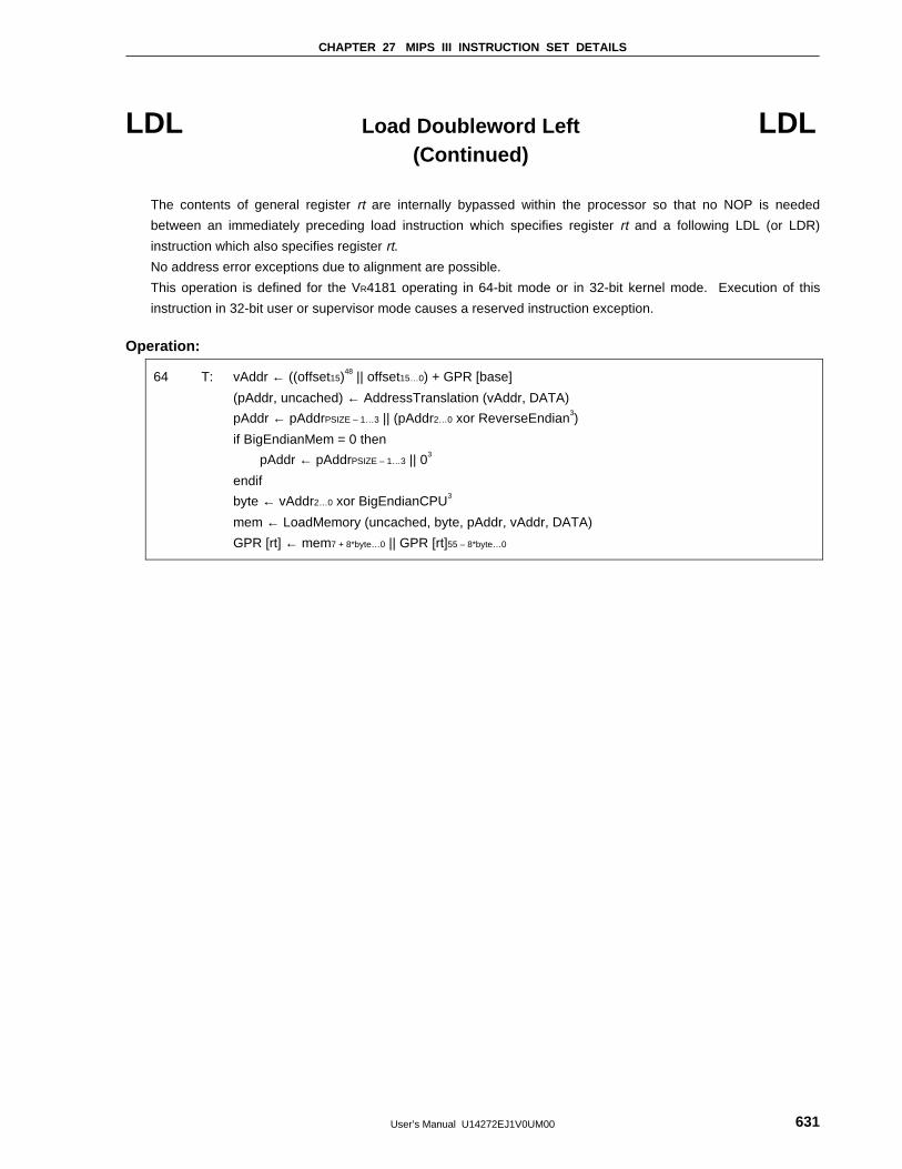
CHAPTER 27 MIPS III INSTRUCTION SET DETAILS
User’s Manual U14272EJ1V0UM00 631
LDL Load Doubleword Left LDL(Continued)
The contents of general register rt are internally bypassed within the processor so that no NOP is needed
between an immediately preceding load instruction which specifies register rt and a following LDL (or LDR)
instruction which also specifies register rt.
No address error exceptions due to alignment are possible.
This operation is defined for the VR4181 operating in 64-bit mode or in 32-bit kernel mode. Execution of this
instruction in 32-bit user or supervisor mode causes a reserved instruction exception.
Operation:
64 T: vAddr ← ((offset15)48 || offset15…0) + GPR [base]
(pAddr, uncached) ← AddressTranslation (vAddr, DATA)
pAddr ← pAddrPSIZE – 1…3 || (pAddr2…0 xor ReverseEndian3)
if BigEndianMem = 0 then
pAddr ← pAddrPSIZE – 1…3 || 03
endif
byte ← vAddr2…0 xor BigEndianCPU3
mem ← LoadMemory (uncached, byte, pAddr, vAddr, DATA)
GPR [rt] ← mem7 + 8*byte…0 || GPR [rt]55 – 8*byte…0
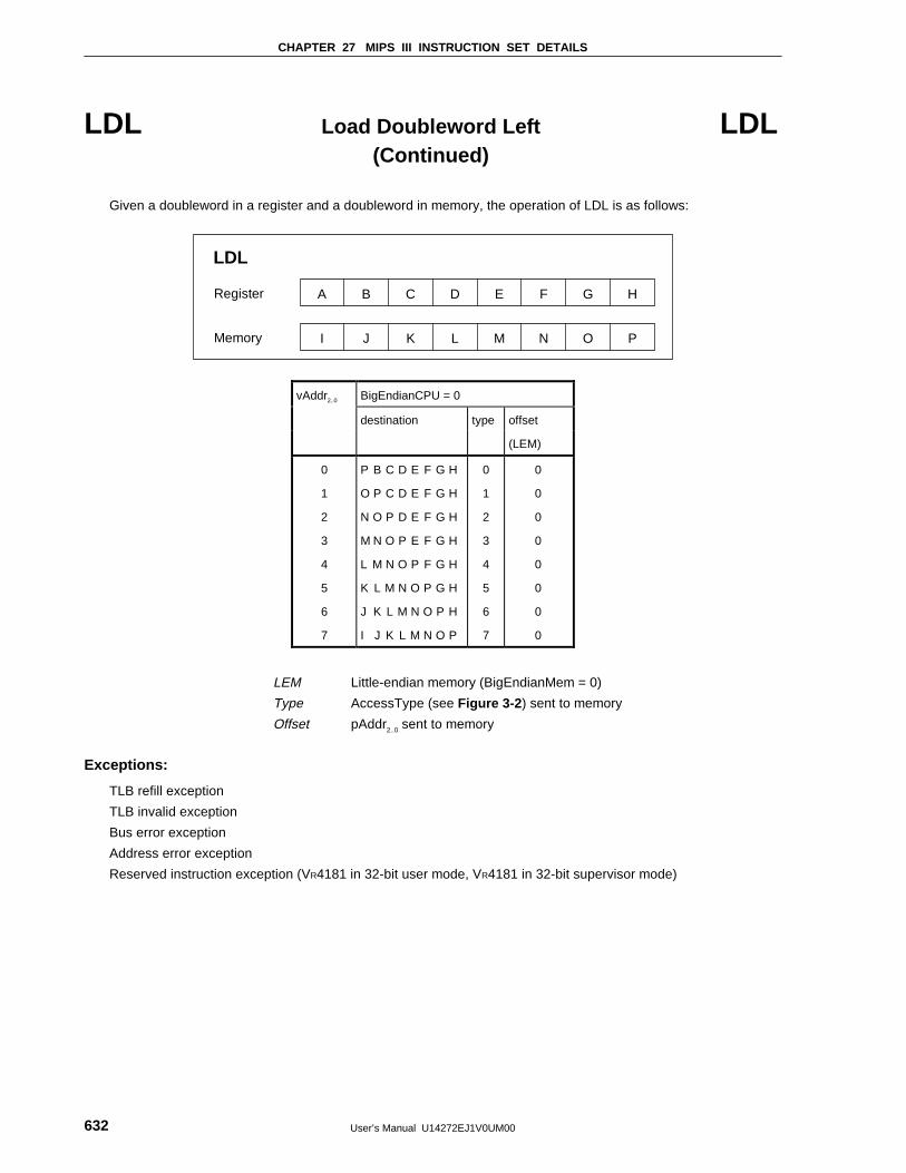
CHAPTER 27 MIPS III INSTRUCTION SET DETAILS
User’s Manual U14272EJ1V0UM00632
LDL Load Doubleword Left LDL(Continued)
Given a doubleword in a register and a doubleword in memory, the operation of LDL is as follows:
B C D E F GA H
J K L M N OI P
Register
Memory
LDL
vAddr2..0 BigEndianCPU = 0
destination type offset
(LEM)
0
1
2
3
4
5
6
7
P B C D E F G H
O P C D E F G H
N O P D E F G H
M N O P E F G H
L M N O P F G H
K L M N O P G H
J K L M N O P H
I J K L M N O P
0
1
2
3
4
5
6
7
0
0
0
0
0
0
0
0
LEM Little-endian memory (BigEndianMem = 0)
Type AccessType (see Figure 3-2 ) sent to memory
Offset pAddr2..0 sent to memory
Exceptions:
TLB refill exception
TLB invalid exception
Bus error exception
Address error exception
Reserved instruction exception (VR4181 in 32-bit user mode, VR4181 in 32-bit supervisor mode)
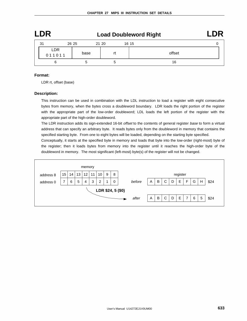
CHAPTER 27 MIPS III INSTRUCTION SET DETAILS
User’s Manual U14272EJ1V0UM00 633
LDR Load Doubleword Right LDR
LDR
31 26 25 21 20 16 15 0
base0 1 1 0 1 1 rt offset
6 5 5 16
Format:
LDR rt, offset (base)
Description:
This instruction can be used in combination with the LDL instruction to load a register with eight consecutive
bytes from memory, when the bytes cross a doubleword boundary. LDR loads the right portion of the register
with the appropriate part of the low-order doubleword; LDL loads the left portion of the register with the
appropriate part of the high-order doubleword.
The LDR instruction adds its sign-extended 16-bit offset to the contents of general register base to form a virtual
address that can specify an arbitrary byte. It reads bytes only from the doubleword in memory that contains the
specified starting byte. From one to eight bytes will be loaded, depending on the starting byte specified.
Conceptually, it starts at the specified byte in memory and loads that byte into the low-order (right-most) byte of
the register; then it loads bytes from memory into the register until it reaches the high-order byte of the
doubleword in memory. The most significant (left-most) byte(s) of the register will not be changed.
address 8
address 0
memory
before
after
$24
$24
register
A B C D E F G H
A B C D E 7 6 5
15 14 13 12 11 10 9 8
7 6 5 4 3 2 1 0
LDR $24, 5 ($0)
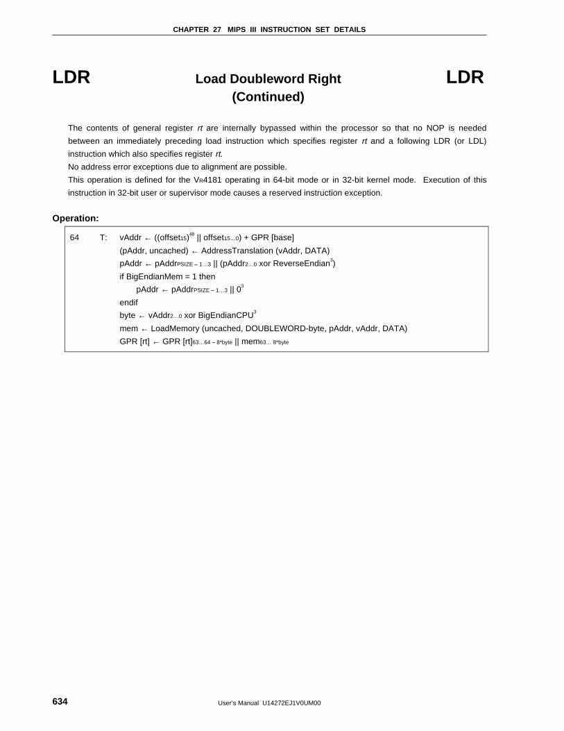
CHAPTER 27 MIPS III INSTRUCTION SET DETAILS
User’s Manual U14272EJ1V0UM00634
LDR Load Doubleword Right LDR(Continued)
The contents of general register rt are internally bypassed within the processor so that no NOP is needed
between an immediately preceding load instruction which specifies register rt and a following LDR (or LDL)
instruction which also specifies register rt.
No address error exceptions due to alignment are possible.
This operation is defined for the VR4181 operating in 64-bit mode or in 32-bit kernel mode. Execution of this
instruction in 32-bit user or supervisor mode causes a reserved instruction exception.
Operation:
64 T: vAddr ← ((offset15)48 || offset15…0) + GPR [base]
(pAddr, uncached) ← AddressTranslation (vAddr, DATA)
pAddr ← pAddrPSIZE – 1…3 || (pAddr2…0 xor ReverseEndian3)
if BigEndianMem = 1 then
pAddr ← pAddrPSIZE – 1…3 || 03
endif
byte ← vAddr2…0 xor BigEndianCPU3
mem ← LoadMemory (uncached, DOUBLEWORD-byte, pAddr, vAddr, DATA)
GPR [rt] ← GPR [rt]63…64 – 8*byte || mem63… 8*byte
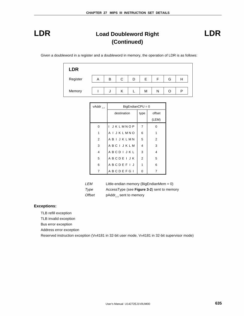
CHAPTER 27 MIPS III INSTRUCTION SET DETAILS
User’s Manual U14272EJ1V0UM00 635
LDR Load Doubleword Right LDR(Continued)
Given a doubleword in a register and a doubleword in memory, the operation of LDR is as follows:
B C D E F GA H
J K L M N OI P
Register
Memory
LDR
vAddr 2..0 BigEndianCPU = 0
destination type offset
(LEM)
0
1
2
3
4
5
6
7
I J K L M N O P
A I J K L M N O
A B I J K L M N
A B C I J K L M
A B C D I J K L
A B C D E I J K
A B C D E F I J
A B C D E F G I
7
6
5
4
3
2
1
0
0
1
2
3
4
5
6
7
LEM Little-endian memory (BigEndianMem = 0)
Type AccessType (see Figure 3-2 ) sent to memory
Offset pAddr2..0 sent to memory
Exceptions:
TLB refill exception
TLB invalid exception
Bus error exception
Address error exception
Reserved instruction exception (VR4181 in 32-bit user mode, VR4181 in 32-bit supervisor mode)
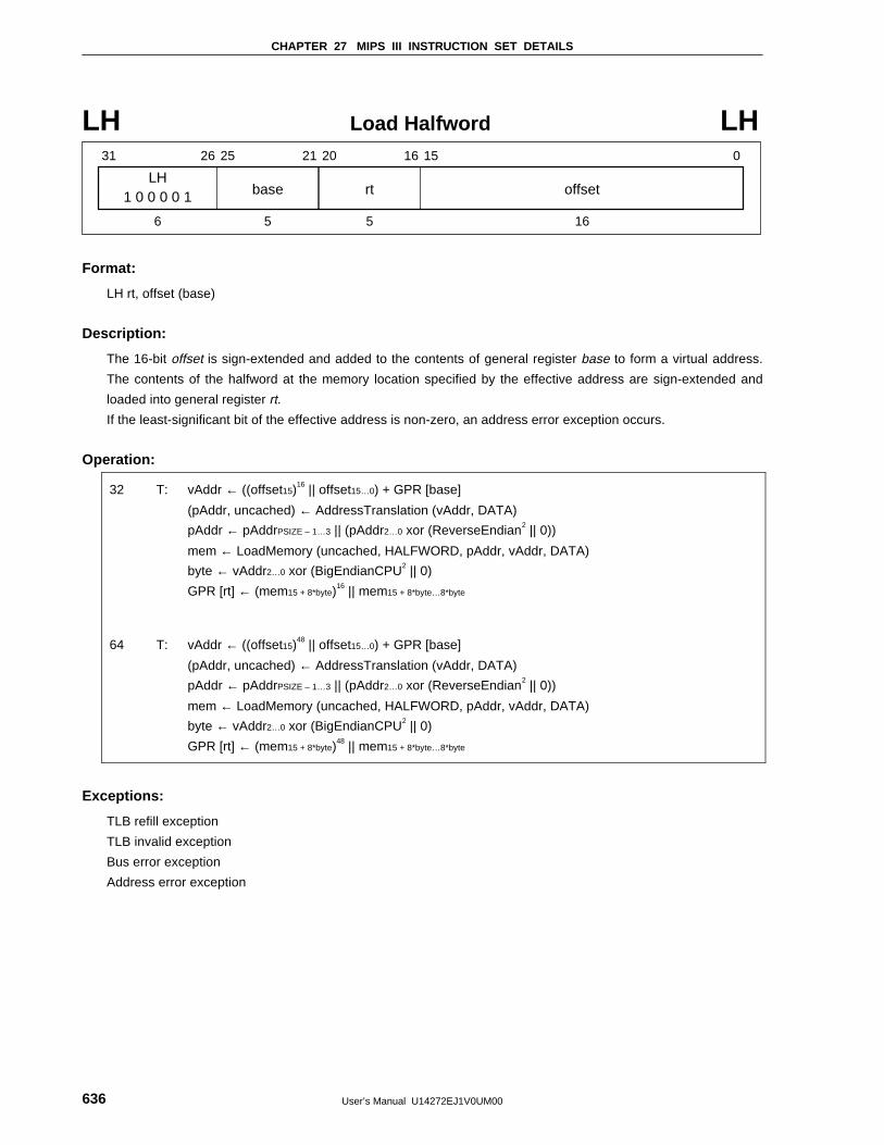
CHAPTER 27 MIPS III INSTRUCTION SET DETAILS
User’s Manual U14272EJ1V0UM00636
LH Load Halfword LH
LH
31 26 25 21 20 16 15 0
base1 0 0 0 0 1 rt offset
6 5 5 16
Format:
LH rt, offset (base)
Description:
The 16-bit offset is sign-extended and added to the contents of general register base to form a virtual address.
The contents of the halfword at the memory location specified by the effective address are sign-extended and
loaded into general register rt.
If the least-significant bit of the effective address is non-zero, an address error exception occurs.
Operation:
32 T: vAddr ← ((offset15)16 || offset15…0) + GPR [base]
(pAddr, uncached) ← AddressTranslation (vAddr, DATA)
pAddr ← pAddrPSIZE – 1…3 || (pAddr2…0 xor (ReverseEndian2 || 0))
mem ← LoadMemory (uncached, HALFWORD, pAddr, vAddr, DATA)
byte ← vAddr2…0 xor (BigEndianCPU2 || 0)
GPR [rt] ← (mem15 + 8*byte)16 || mem15 + 8*byte…8*byte
64 T: vAddr ← ((offset15)48 || offset15…0) + GPR [base]
(pAddr, uncached) ← AddressTranslation (vAddr, DATA)
pAddr ← pAddrPSIZE – 1…3 || (pAddr2…0 xor (ReverseEndian2 || 0))
mem ← LoadMemory (uncached, HALFWORD, pAddr, vAddr, DATA)
byte ← vAddr2…0 xor (BigEndianCPU2 || 0)
GPR [rt] ← (mem15 + 8*byte)48 || mem15 + 8*byte…8*byte
Exceptions:
TLB refill exception
TLB invalid exception
Bus error exception
Address error exception
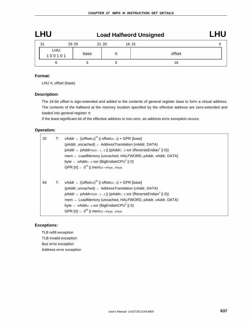
CHAPTER 27 MIPS III INSTRUCTION SET DETAILS
User’s Manual U14272EJ1V0UM00 637
LHU Load Halfword Unsigned LHU
LHU
31 26 25 21 20 16 15 0
base1 0 0 1 0 1 rt offset
6 5 5 16
Format:
LHU rt, offset (base)
Description:
The 16-bit offset is sign-extended and added to the contents of general register base to form a virtual address.
The contents of the halfword at the memory location specified by the effective address are zero-extended and
loaded into general register rt.
If the least-significant bit of the effective address is non-zero, an address error exception occurs.
Operation:
32 T: vAddr ← ((offset15)16 || offset15…0) + GPR [base]
(pAddr, uncached) ← AddressTranslation (vAddr, DATA)
pAddr ← pAddrPSIZE – 1…3 || (pAddr2…0 xor (ReverseEndian2 || 0))
mem ← LoadMemory (uncached, HALFWORD, pAddr, vAddr, DATA)
byte ← vAddr2…0 xor (BigEndianCPU2 || 0)
GPR [rt] ← 016 || mem15 + 8*byte…8*byte
64 T: vAddr ← ((offset15)48 || offset15…0) + GPR [base]
(pAddr, uncached) ← AddressTranslation (vAddr, DATA)
pAddr ← pAddrPSIZE – 1…3 || (pAddr2…0 xor (ReverseEndian2 || 0))
mem ← LoadMemory (uncached, HALFWORD, pAddr, vAddr, DATA)
byte ← vAddr2…0 xor (BigEndianCPU2 || 0)
GPR [rt] ← 048 || mem15 + 8*byte…8*byte
Exceptions:
TLB refill exception
TLB invalid exception
Bus error exception
Address error exception
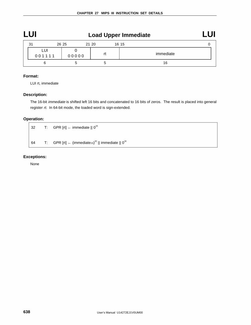
CHAPTER 27 MIPS III INSTRUCTION SET DETAILS
User’s Manual U14272EJ1V0UM00638
LUI Load Upper Immediate LUI
LUI
31 26 25 21 20 16 15 0
0 0 1 1 1 1 rt immediate
6 5 5 16
00 0 0 0 0
Format:
LUI rt, immediate
Description:
The 16-bit immediate is shifted left 16 bits and concatenated to 16 bits of zeros. The result is placed into general
register rt. In 64-bit mode, the loaded word is sign-extended.
Operation:
32 T: GPR [rt] ← immediate || 016
64 T: GPR [rt] ← (immediate15)32 || immediate || 016
Exceptions:
None
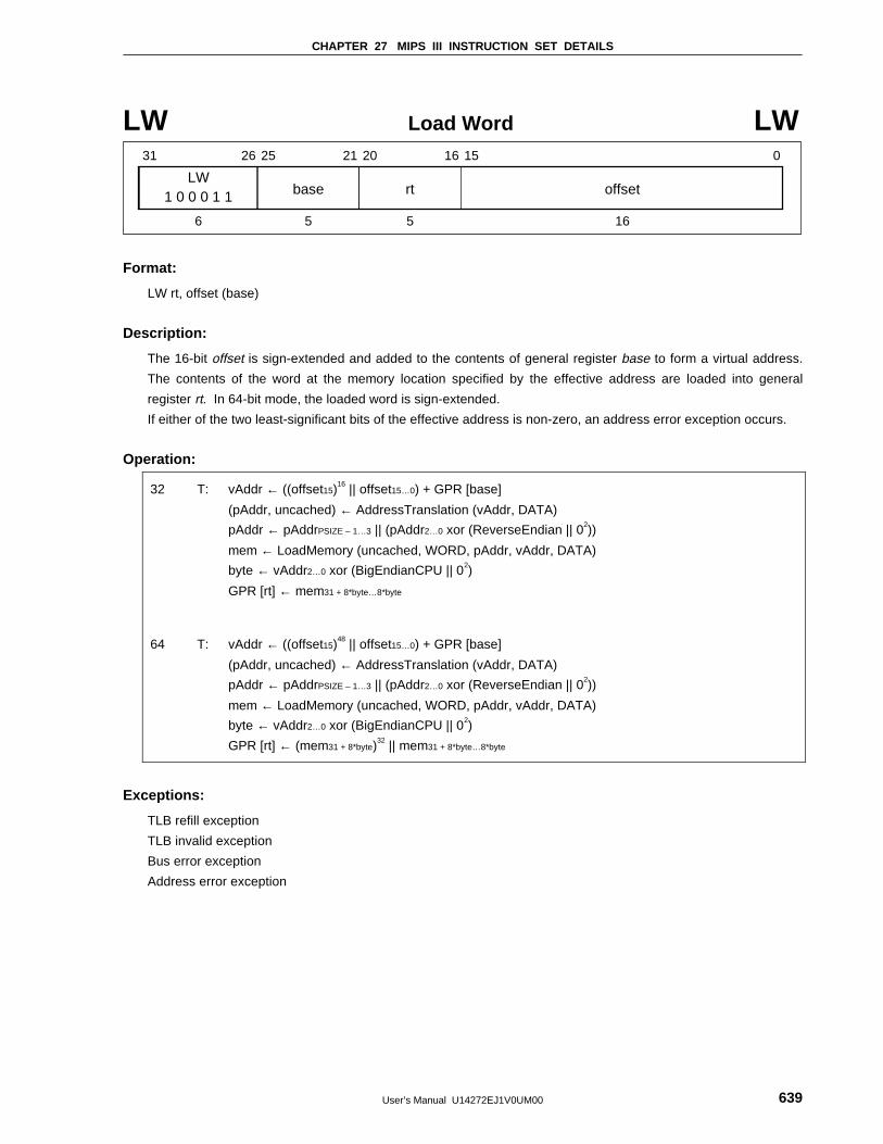
CHAPTER 27 MIPS III INSTRUCTION SET DETAILS
User’s Manual U14272EJ1V0UM00 639
LW Load Word LW
LW
31 26 25 21 20 16 15 0
base1 0 0 0 1 1 rt offset
6 5 5 16
Format:
LW rt, offset (base)
Description:
The 16-bit offset is sign-extended and added to the contents of general register base to form a virtual address.
The contents of the word at the memory location specified by the effective address are loaded into general
register rt. In 64-bit mode, the loaded word is sign-extended.
If either of the two least-significant bits of the effective address is non-zero, an address error exception occurs.
Operation:
32 T: vAddr ← ((offset15)16 || offset15…0) + GPR [base]
(pAddr, uncached) ← AddressTranslation (vAddr, DATA)
pAddr ← pAddrPSIZE – 1…3 || (pAddr2…0 xor (ReverseEndian || 02))
mem ← LoadMemory (uncached, WORD, pAddr, vAddr, DATA)
byte ← vAddr2…0 xor (BigEndianCPU || 02)
GPR [rt] ← mem31 + 8*byte…8*byte
64 T: vAddr ← ((offset15)48 || offset15…0) + GPR [base]
(pAddr, uncached) ← AddressTranslation (vAddr, DATA)
pAddr ← pAddrPSIZE – 1…3 || (pAddr2…0 xor (ReverseEndian || 02))
mem ← LoadMemory (uncached, WORD, pAddr, vAddr, DATA)
byte ← vAddr2…0 xor (BigEndianCPU || 02)
GPR [rt] ← (mem31 + 8*byte)32 || mem31 + 8*byte…8*byte
Exceptions:
TLB refill exception
TLB invalid exception
Bus error exception
Address error exception
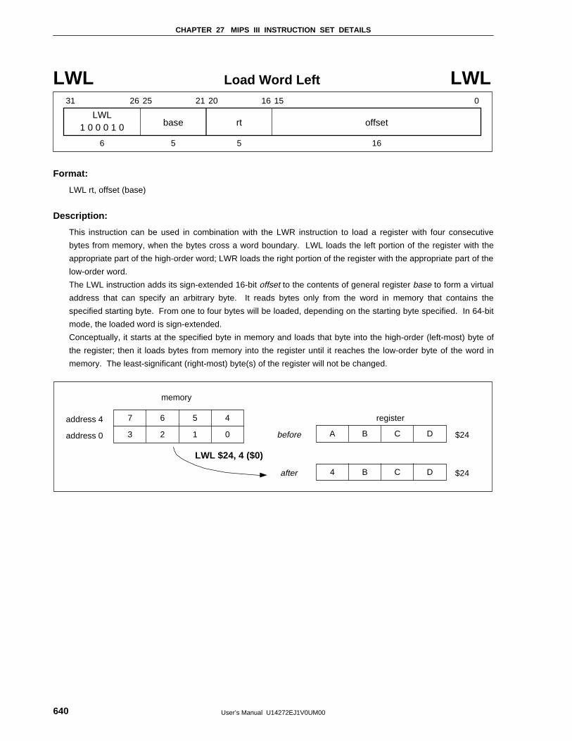
CHAPTER 27 MIPS III INSTRUCTION SET DETAILS
User’s Manual U14272EJ1V0UM00640
LWL Load Word Left LWL
LWL
31 26 25 21 20 16 15 0
base1 0 0 0 1 0 rt offset
6 5 5 16
Format:
LWL rt, offset (base)
Description:
This instruction can be used in combination with the LWR instruction to load a register with four consecutive
bytes from memory, when the bytes cross a word boundary. LWL loads the left portion of the register with the
appropriate part of the high-order word; LWR loads the right portion of the register with the appropriate part of the
low-order word.
The LWL instruction adds its sign-extended 16-bit offset to the contents of general register base to form a virtual
address that can specify an arbitrary byte. It reads bytes only from the word in memory that contains the
specified starting byte. From one to four bytes will be loaded, depending on the starting byte specified. In 64-bit
mode, the loaded word is sign-extended.
Conceptually, it starts at the specified byte in memory and loads that byte into the high-order (left-most) byte of
the register; then it loads bytes from memory into the register until it reaches the low-order byte of the word in
memory. The least-significant (right-most) byte(s) of the register will not be changed.
address 4
address 0
memory
7
before
after
$24
$24
register
LWL $24, 4 ($0)
6 5 4
3 2 1 0 A B C D
4 B C D
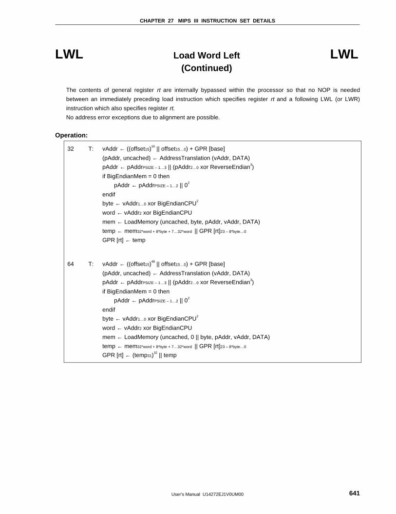
CHAPTER 27 MIPS III INSTRUCTION SET DETAILS
User’s Manual U14272EJ1V0UM00 641
LWL Load Word Left LWL(Continued)
The contents of general register rt are internally bypassed within the processor so that no NOP is needed
between an immediately preceding load instruction which specifies register rt and a following LWL (or LWR)
instruction which also specifies register rt.
No address error exceptions due to alignment are possible.
Operation:
32 T: vAddr ← ((offset15)16 || offset15…0) + GPR [base]
(pAddr, uncached) ← AddressTranslation (vAddr, DATA)
pAddr ← pAddrPSIZE – 1…3 || (pAddr2…0 xor ReverseEndian3)
if BigEndianMem = 0 then
pAddr ← pAddrPSIZE – 1…2 || 02
endif
byte ← vAddr1…0 xor BigEndianCPU2
word ← vAddr2 xor BigEndianCPU
mem ← LoadMemory (uncached, byte, pAddr, vAddr, DATA)
temp ← mem32*word + 8*byte + 7…32*word || GPR [rt]23 – 8*byte…0
GPR [rt] ← temp
64 T: vAddr ← ((offset15)48 || offset15…0) + GPR [base]
(pAddr, uncached) ← AddressTranslation (vAddr, DATA)
pAddr ← pAddrPSIZE – 1…3 || (pAddr2…0 xor ReverseEndian3)
if BigEndianMem = 0 then
pAddr ← pAddrPSIZE – 1…2 || 02
endif
byte ← vAddr1…0 xor BigEndianCPU2
word ← vAddr2 xor BigEndianCPU
mem ← LoadMemory (uncached, 0 || byte, pAddr, vAddr, DATA)
temp ← mem32*word + 8*byte + 7…32*word || GPR [rt]23 – 8*byte…0
GPR [rt] ← (temp31)32 || temp
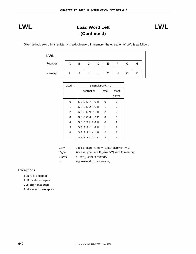
CHAPTER 27 MIPS III INSTRUCTION SET DETAILS
User’s Manual U14272EJ1V0UM00642
LWL Load Word Left LWL(Continued)
Given a doubleword in a register and a doubleword in memory, the operation of LWL is as follows:
B C D E F GA H
J K L M N OI P
Register
Memory
LWL
vAddr2..0 BigEndianCPU = 0
destination type offset
(LEM)
0
1
2
3
4
5
6
7
S S S S P F G H
S S S S O P G H
S S S S N O P H
S S S S M N O P
S S S S L F G H
S S S S K L G H
S S S S J K L H
S S S S I J K L
0
1
2
3
0
1
2
3
0
0
0
0
4
4
4
4
LEM Little-endian memory (BigEndianMem = 0)
Type AccessType (see Figure 3-2 ) sent to memory
Offset pAddr2...0 sent to memory
S sign-extend of destination31
Exceptions:
TLB refill exception
TLB invalid exception
Bus error exception
Address error exception
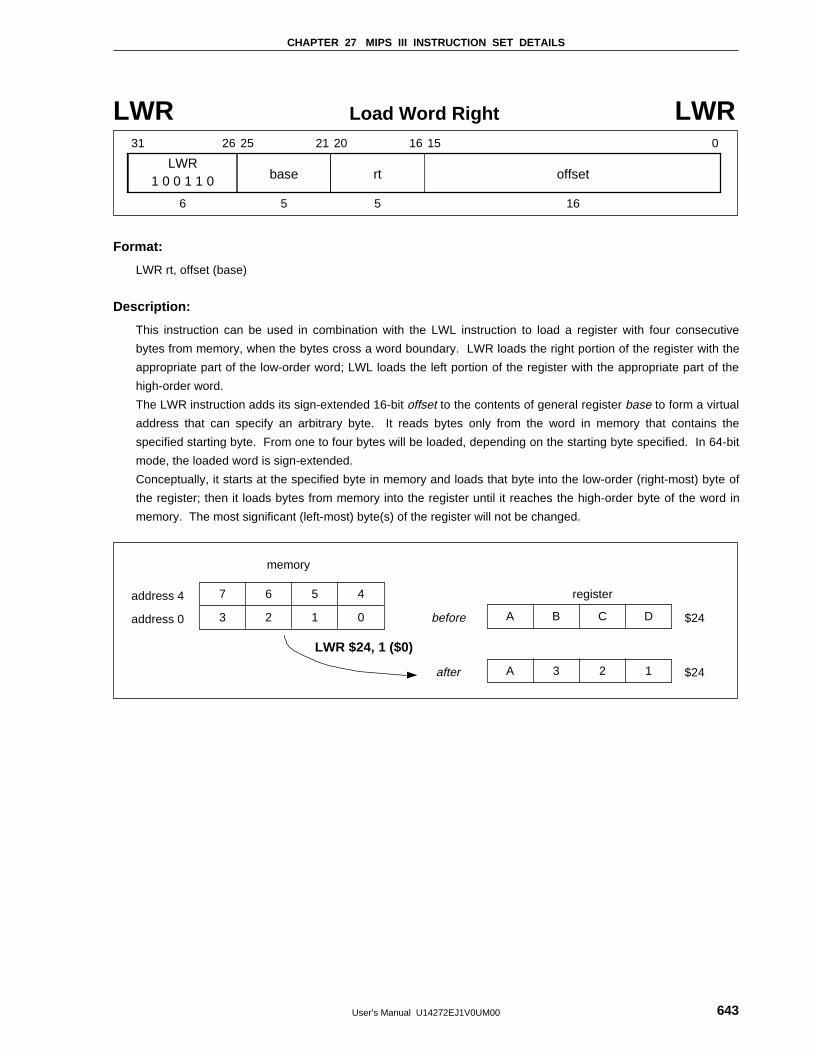
CHAPTER 27 MIPS III INSTRUCTION SET DETAILS
User’s Manual U14272EJ1V0UM00 643
LWR Load Word Right LWR
LWR
31 26 25 21 20 16 15 0
base1 0 0 1 1 0 rt offset
6 5 5 16
Format:
LWR rt, offset (base)
Description:
This instruction can be used in combination with the LWL instruction to load a register with four consecutive
bytes from memory, when the bytes cross a word boundary. LWR loads the right portion of the register with the
appropriate part of the low-order word; LWL loads the left portion of the register with the appropriate part of the
high-order word.
The LWR instruction adds its sign-extended 16-bit offset to the contents of general register base to form a virtual
address that can specify an arbitrary byte. It reads bytes only from the word in memory that contains the
specified starting byte. From one to four bytes will be loaded, depending on the starting byte specified. In 64-bit
mode, the loaded word is sign-extended.
Conceptually, it starts at the specified byte in memory and loads that byte into the low-order (right-most) byte of
the register; then it loads bytes from memory into the register until it reaches the high-order byte of the word in
memory. The most significant (left-most) byte(s) of the register will not be changed.
address 4
address 0
memory
7
before
after
$24
$24
register
LWR $24, 1 ($0)
6 5 4
3 2 1 0 A B C D
A 3 2 1
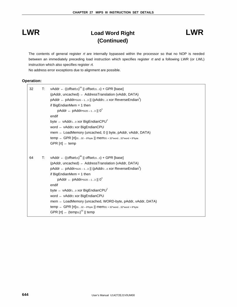
CHAPTER 27 MIPS III INSTRUCTION SET DETAILS
User’s Manual U14272EJ1V0UM00644
LWR Load Word Right LWR(Continued)
The contents of general register rt are internally bypassed within the processor so that no NOP is needed
between an immediately preceding load instruction which specifies register rt and a following LWR (or LWL)
instruction which also specifies register rt.
No address error exceptions due to alignment are possible.
Operation:
32 T: vAddr ← ((offset15)16 || offset15…0) + GPR [base]
(pAddr, uncached) ← AddressTranslation (vAddr, DATA)
pAddr ← pAddrPSIZE – 1…3 || (pAddr2…0 xor ReverseEndian3)
if BigEndianMem = 1 then
pAddr ← pAddrPSIZE – 1…3 || 03
endif
byte ← vAddr1…0 xor BigEndianCPU2
word ← vAddr2 xor BigEndianCPU
mem ← LoadMemory (uncached, 0 || byte, pAddr, vAddr, DATA)
temp ← GPR [rt]31…32 – 8*byte || mem31 + 32*word…32*word + 8*byte
GPR [rt] ← temp
64 T: vAddr ← ((offset15)48 || offset15…0) + GPR [base]
(pAddr, uncached) ← AddressTranslation (vAddr, DATA)
pAddr ← pAddrPSIZE – 1…3 || (pAddr2…0 xor ReverseEndian3)
if BigEndianMem = 1 then
pAddr ← pAddrPSIZE – 1…3 || 03
endif
byte ← vAddr1…0 xor BigEndianCPU2
word ← vAddr2 xor BigEndianCPU
mem ← LoadMemory (uncached, WORD-byte, pAddr, vAddr, DATA)
temp ← GPR [rt]31…32 – 8*byte || mem31 + 32*word…32*word + 8*byte
GPR [rt] ← (temp31)32 || temp
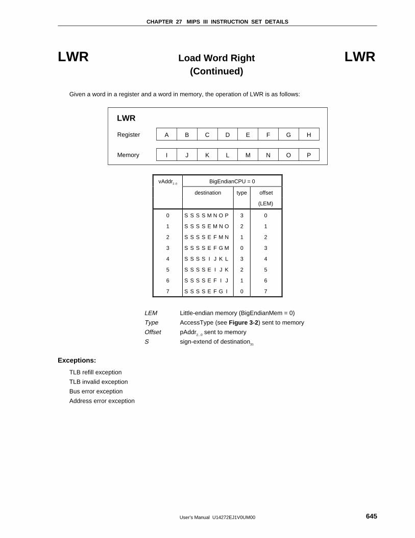
CHAPTER 27 MIPS III INSTRUCTION SET DETAILS
User’s Manual U14272EJ1V0UM00 645
LWR Load Word Right LWR(Continued)
Given a word in a register and a word in memory, the operation of LWR is as follows:
B C D E F GA H
J K L M N OI P
Register
Memory
LWR
vAddr2..0 BigEndianCPU = 0
destination type offset
(LEM)
0
1
2
3
4
5
6
7
S S S S M N O P
S S S S E M N O
S S S S E F M N
S S S S E F G M
S S S S I J K L
S S S S E I J K
S S S S E F I J
S S S S E F G I
3
2
1
0
3
2
1
0
0
1
2
3
4
5
6
7
LEM Little-endian memory (BigEndianMem = 0)
Type AccessType (see Figure 3-2 ) sent to memory
Offset pAddr2...0 sent to memory
S sign-extend of destination31
Exceptions:
TLB refill exception
TLB invalid exception
Bus error exception
Address error exception
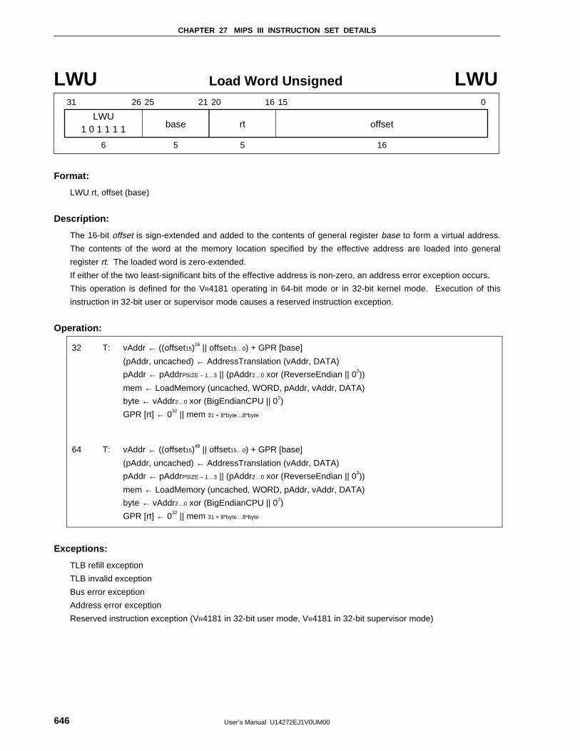
CHAPTER 27 MIPS III INSTRUCTION SET DETAILS
User’s Manual U14272EJ1V0UM00646
LWU Load Word Unsigned LWU
LWU
31 26 25 21 20 16 15 0
base1 0 1 1 1 1 rt offset
6 5 5 16
Format:
LWU rt, offset (base)
Description:
The 16-bit offset is sign-extended and added to the contents of general register base to form a virtual address.
The contents of the word at the memory location specified by the effective address are loaded into general
register rt. The loaded word is zero-extended.
If either of the two least-significant bits of the effective address is non-zero, an address error exception occurs.
This operation is defined for the VR4181 operating in 64-bit mode or in 32-bit kernel mode. Execution of this
instruction in 32-bit user or supervisor mode causes a reserved instruction exception.
Operation:
32 T: vAddr ← ((offset15)16 || offset15…0) + GPR [base]
(pAddr, uncached) ← AddressTranslation (vAddr, DATA)
pAddr ← pAddrPSIZE – 1…3 || (pAddr2…0 xor (ReverseEndian || 02))
mem ← LoadMemory (uncached, WORD, pAddr, vAddr, DATA)
byte ← vAddr2…0 xor (BigEndianCPU || 02)
GPR [rt] ← 032 || mem 31 + 8*byte…8*byte
64 T: vAddr ← ((offset15)48 || offset15…0) + GPR [base]
(pAddr, uncached) ← AddressTranslation (vAddr, DATA)
pAddr ← pAddrPSIZE – 1…3 || (pAddr2…0 xor (ReverseEndian || 02))
mem ← LoadMemory (uncached, WORD, pAddr, vAddr, DATA)
byte ← vAddr2…0 xor (BigEndianCPU || 02)
GPR [rt] ← 032 || mem 31 + 8*byte…8*byte
Exceptions:
TLB refill exception
TLB invalid exception
Bus error exception
Address error exception
Reserved instruction exception (VR4181 in 32-bit user mode, VR4181 in 32-bit supervisor mode)
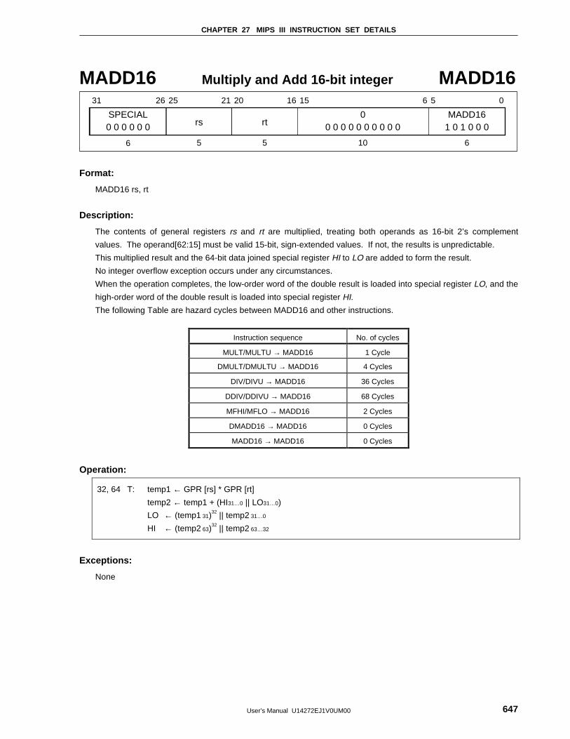
CHAPTER 27 MIPS III INSTRUCTION SET DETAILS
User’s Manual U14272EJ1V0UM00 647
MADD16 Multiply and Add 16-bit integer MADD16
SPECIAL
31 26 25 21 20 16 15 6 5 0
rs0 0 0 0 0 0 rt0
0 0 0 0 0 0 0 0 0 0MADD16
1 0 1 0 0 0
6 5 5 10 6
Format:
MADD16 rs, rt
Description:
The contents of general registers rs and rt are multiplied, treating both operands as 16-bit 2’s complement
values. The operand[62:15] must be valid 15-bit, sign-extended values. If not, the results is unpredictable.
This multiplied result and the 64-bit data joined special register HI to LO are added to form the result.
No integer overflow exception occurs under any circumstances.
When the operation completes, the low-order word of the double result is loaded into special register LO, and the
high-order word of the double result is loaded into special register HI.
The following Table are hazard cycles between MADD16 and other instructions.
Instruction sequence No. of cycles
MULT/MULTU → MADD16 1 Cycle
DMULT/DMULTU → MADD16 4 Cycles
DIV/DIVU → MADD16 36 Cycles
DDIV/DDIVU → MADD16 68 Cycles
MFHI/MFLO → MADD16 2 Cycles
DMADD16 → MADD16 0 Cycles
MADD16 → MADD16 0 Cycles
Operation:
32, 64 T: temp1 ← GPR [rs] * GPR [rt]
temp2 ← temp1 + (HI31…0 || LO31…0)
LO ← (temp1 31)32 || temp2 31…0
HI ← (temp2 63)32 || temp2 63…32
Exceptions:
None
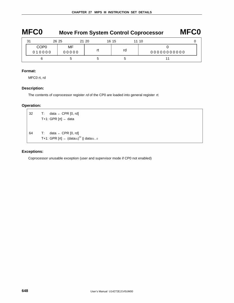
CHAPTER 27 MIPS III INSTRUCTION SET DETAILS
User’s Manual U14272EJ1V0UM00648
MFC0 Move From System Control Coprocessor MFC0
COP0
31 26 25 21 20 16 15 11 10 0
0 1 0 0 0 0 rt rdMF
0 0 0 0 00
0 0 0 0 0 0 0 0 0 0 0
6 5 5 5 11
Format:
MFC0 rt, rd
Description:
The contents of coprocessor register rd of the CP0 are loaded into general register rt.
Operation:
32 T: data ← CPR [0, rd]
T+1: GPR [rt] ← data
64 T: data ← CPR [0, rd]
T+1: GPR [rt] ← (data31)32 || data31…0
Exceptions:
Coprocessor unusable exception (user and supervisor mode if CP0 not enabled)
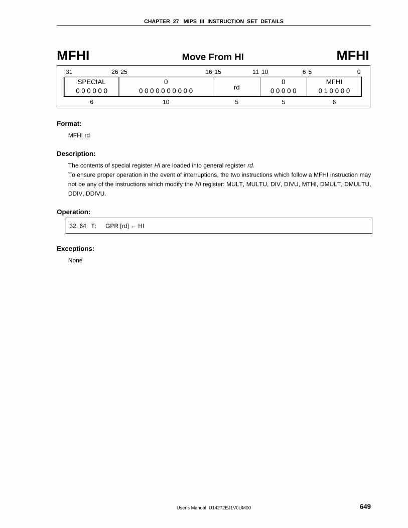
CHAPTER 27 MIPS III INSTRUCTION SET DETAILS
User’s Manual U14272EJ1V0UM00 649
MFHI Move From HI MFHI
SPECIAL
31 26 25 16 15 11 10 6 5 0
0 0 0 0 0 0 rd0
0 0 0 0 0MFHI
0 1 0 0 0 0
6 5 5 6
00 0 0 0 0 0 0 0 0 0
10
Format:
MFHI rd
Description:
The contents of special register HI are loaded into general register rd.
To ensure proper operation in the event of interruptions, the two instructions which follow a MFHI instruction may
not be any of the instructions which modify the HI register: MULT, MULTU, DIV, DIVU, MTHI, DMULT, DMULTU,
DDIV, DDIVU.
Operation:
32, 64 T: GPR [rd] ← HI
Exceptions:
None
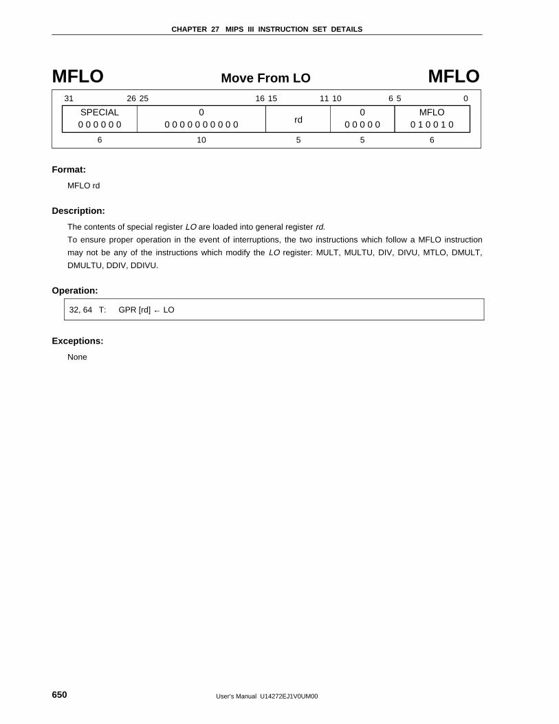
CHAPTER 27 MIPS III INSTRUCTION SET DETAILS
User’s Manual U14272EJ1V0UM00650
MFLO Move From LO MFLO
SPECIAL
31 26 25 16 15 11 10 6 5 0
0 0 0 0 0 0 rd0
0 0 0 0 0MFLO
0 1 0 0 1 0
6 5 5 6
00 0 0 0 0 0 0 0 0 0
10
Format:
MFLO rd
Description:
The contents of special register LO are loaded into general register rd.
To ensure proper operation in the event of interruptions, the two instructions which follow a MFLO instruction
may not be any of the instructions which modify the LO register: MULT, MULTU, DIV, DIVU, MTLO, DMULT,
DMULTU, DDIV, DDIVU.
Operation:
32, 64 T: GPR [rd] ← LO
Exceptions:
None
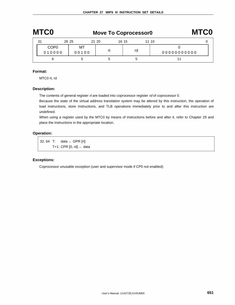
CHAPTER 27 MIPS III INSTRUCTION SET DETAILS
User’s Manual U14272EJ1V0UM00 651
MTC0 Move To Coprocessor0 MTC0
COP0
31 26 25 21 20 16 15 11 10 0
0 1 0 0 0 0 rt rdMT
0 0 1 0 00
0 0 0 0 0 0 0 0 0 0 0
6 5 5 5 11
Format:
MTC0 rt, rd
Description:
The contents of general register rt are loaded into coprocessor register rd of coprocessor 0.
Because the state of the virtual address translation system may be altered by this instruction, the operation of
load instructions, store instructions, and TLB operations immediately prior to and after this instruction are
undefined.
When using a register used by the MTC0 by means of instructions before and after it, refer to Chapter 29 and
place the instructions in the appropriate location.
Operation:
32, 64 T: data ← GPR [rt]
T+1: CPR [0, rd] ← data
Exceptions:
Coprocessor unusable exception (user and supervisor mode if CP0 not enabled)
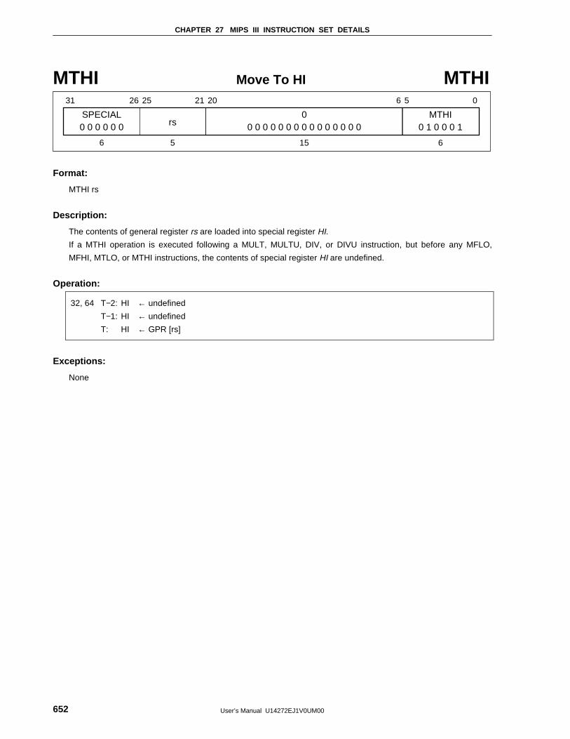
CHAPTER 27 MIPS III INSTRUCTION SET DETAILS
User’s Manual U14272EJ1V0UM00652
MTHI Move To HI MTHI
SPECIAL
31 26 25 21 20 6 5 0
rs0 0 0 0 0 00
0 0 0 0 0 0 0 0 0 0 0 0 0 0 0MTHI
0 1 0 0 0 1
6 5 15 6
Format:
MTHI rs
Description:
The contents of general register rs are loaded into special register HI.
If a MTHI operation is executed following a MULT, MULTU, DIV, or DIVU instruction, but before any MFLO,
MFHI, MTLO, or MTHI instructions, the contents of special register HI are undefined.
Operation:
32, 64 T−2: HI ← undefined
T−1: HI ← undefined
T: HI ← GPR [rs]
Exceptions:
None
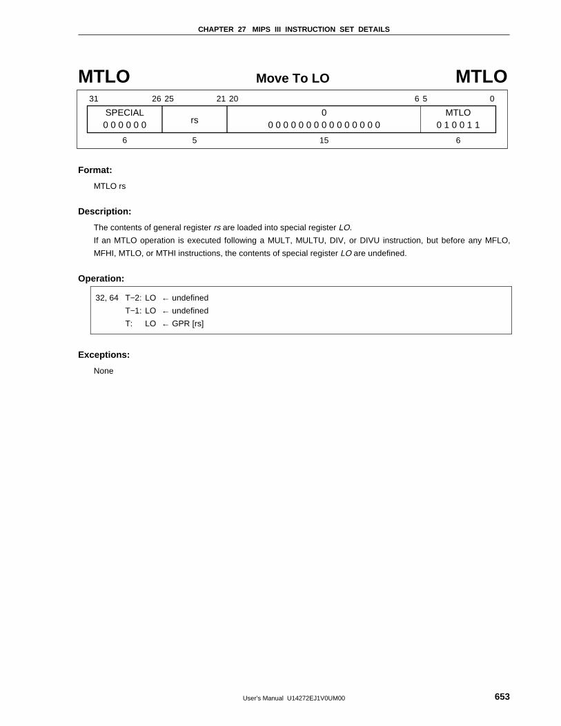
CHAPTER 27 MIPS III INSTRUCTION SET DETAILS
User’s Manual U14272EJ1V0UM00 653
MTLO Move To LO MTLO
SPECIAL
31 26 25 21 20 6 5 0
rs0 0 0 0 0 00
0 0 0 0 0 0 0 0 0 0 0 0 0 0 0MTLO
0 1 0 0 1 1
6 5 15 6
Format:
MTLO rs
Description:
The contents of general register rs are loaded into special register LO.
If an MTLO operation is executed following a MULT, MULTU, DIV, or DIVU instruction, but before any MFLO,
MFHI, MTLO, or MTHI instructions, the contents of special register LO are undefined.
Operation:
32, 64 T−2: LO ← undefined
T−1: LO ← undefined
T: LO ← GPR [rs]
Exceptions:
None
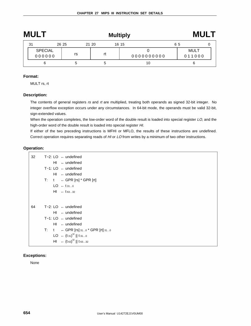
CHAPTER 27 MIPS III INSTRUCTION SET DETAILS
User’s Manual U14272EJ1V0UM00654
MULT Multiply MULT
SPECIAL
31 26 25 21 20 16 15 6 5 0
rs0 0 0 0 0 0 rt0
0 0 0 0 0 0 0 0 0 0MULT
0 1 1 0 0 0
6 5 5 10 6
Format:
MULT rs, rt
Description:
The contents of general registers rs and rt are multiplied, treating both operands as signed 32-bit integer. No
integer overflow exception occurs under any circumstances. In 64-bit mode, the operands must be valid 32-bit,
sign-extended values.
When the operation completes, the low-order word of the double result is loaded into special register LO, and the
high-order word of the double result is loaded into special register HI.
If either of the two preceding instructions is MFHI or MFLO, the results of these instructions are undefined.
Correct operation requires separating reads of HI or LO from writes by a minimum of two other instructions.
Operation:
32 T−2: LO ← undefined
HI ← undefined
T−1: LO ← undefined
HI ← undefined
T: t ← GPR [rs] * GPR [rt]
LO ← t 31…0
HI ← t 63…32
64 T−2: LO ← undefined
HI ← undefined
T−1: LO ← undefined
HI ← undefined
T: t ← GPR [rs] 31…0 * GPR [rt] 31…0
LO ← (t 31)32 || t 31…0
HI ← (t 63)32 || t 63…32
Exceptions:
None
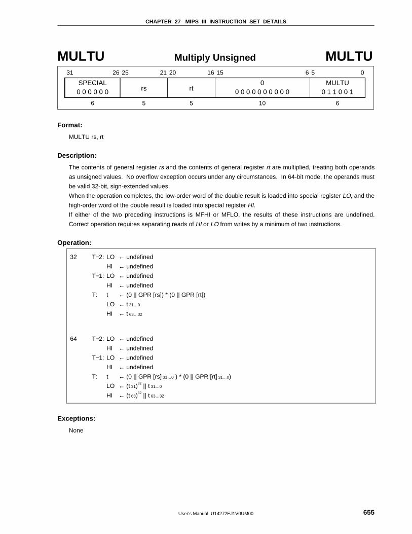
CHAPTER 27 MIPS III INSTRUCTION SET DETAILS
User’s Manual U14272EJ1V0UM00 655
MULTU Multiply Unsigned MULTU
SPECIAL
31 26 25 21 20 16 15 6 5 0
rs0 0 0 0 0 0 rt0
0 0 0 0 0 0 0 0 0 0MULTU
0 1 1 0 0 1
6 5 5 10 6
Format:
MULTU rs, rt
Description:
The contents of general register rs and the contents of general register rt are multiplied, treating both operands
as unsigned values. No overflow exception occurs under any circumstances. In 64-bit mode, the operands must
be valid 32-bit, sign-extended values.
When the operation completes, the low-order word of the double result is loaded into special register LO, and the
high-order word of the double result is loaded into special register HI.
If either of the two preceding instructions is MFHI or MFLO, the results of these instructions are undefined.
Correct operation requires separating reads of HI or LO from writes by a minimum of two instructions.
Operation:
32 T−2: LO ← undefined
HI ← undefined
T−1: LO ← undefined
HI ← undefined
T: t ← (0 || GPR [rs]) * (0 || GPR [rt])
LO ← t 31…0
HI ← t 63…32
64 T−2: LO ← undefined
HI ← undefined
T−1: LO ← undefined
HI ← undefined
T: t ← (0 || GPR [rs] 31…0 ) * (0 || GPR [rt] 31…0)
LO ← (t 31)32 || t 31…0
HI ← (t 63)32 || t 63…32
Exceptions:
None
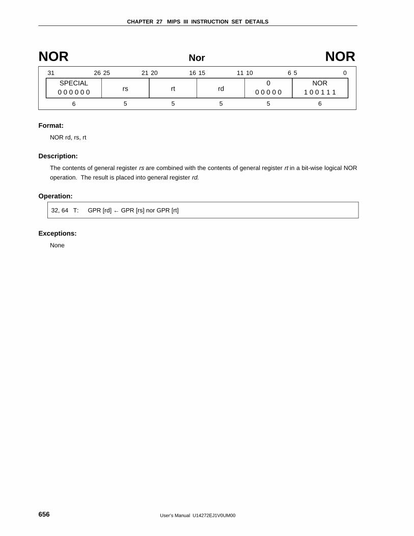
CHAPTER 27 MIPS III INSTRUCTION SET DETAILS
User’s Manual U14272EJ1V0UM00656
NOR Nor NOR
SPECIAL
31 26 25 21 20 16 15 11 10 6 5 0
rs0 0 0 0 0 0 rt rd0
0 0 0 0 0NOR
1 0 0 1 1 1
6 5 5 5 5 6
Format:
NOR rd, rs, rt
Description:
The contents of general register rs are combined with the contents of general register rt in a bit-wise logical NOR
operation. The result is placed into general register rd.
Operation:
32, 64 T: GPR [rd] ← GPR [rs] nor GPR [rt]
Exceptions:
None
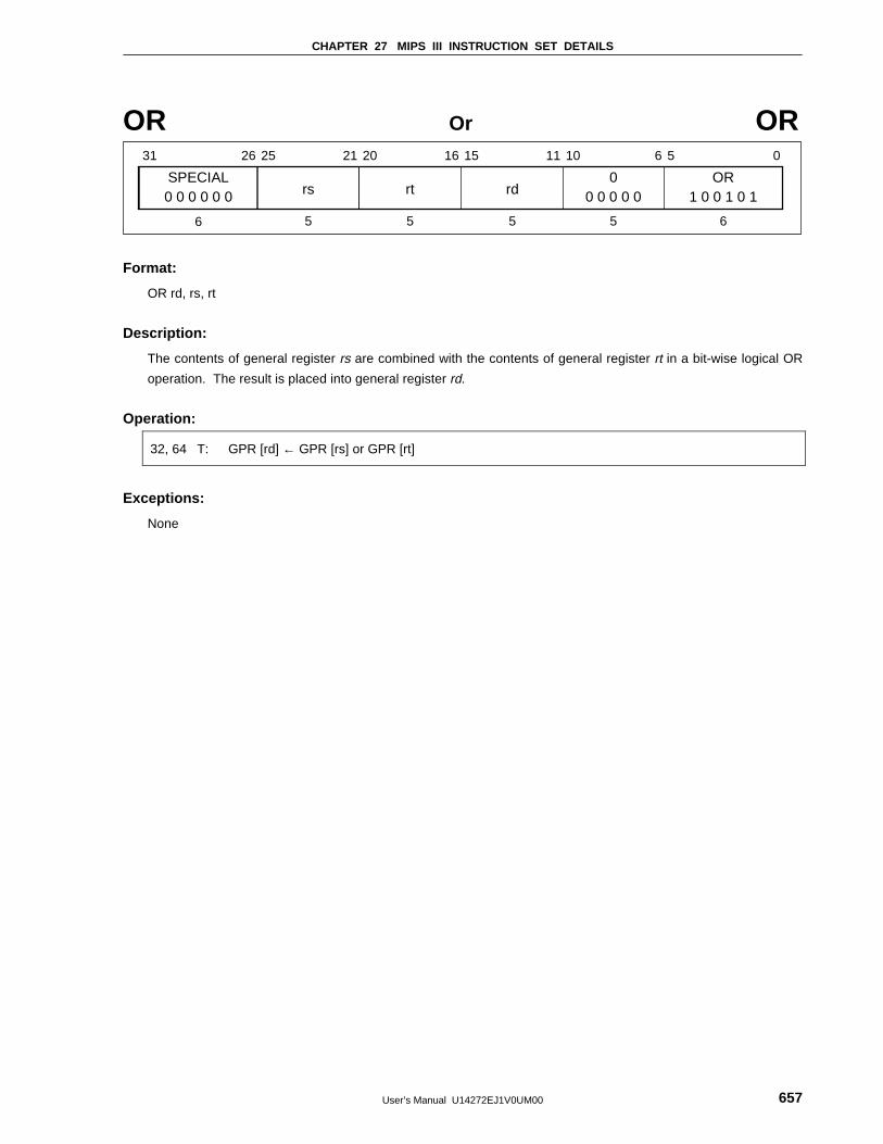
CHAPTER 27 MIPS III INSTRUCTION SET DETAILS
User’s Manual U14272EJ1V0UM00 657
OR Or OR
SPECIAL
31 26 25 21 20 16 15 11 10 6 5 0
rs0 0 0 0 0 0 rt rd0
0 0 0 0 0OR
1 0 0 1 0 1
6 5 5 5 5 6
Format:
OR rd, rs, rt
Description:
The contents of general register rs are combined with the contents of general register rt in a bit-wise logical OR
operation. The result is placed into general register rd.
Operation:
32, 64 T: GPR [rd] ← GPR [rs] or GPR [rt]
Exceptions:
None
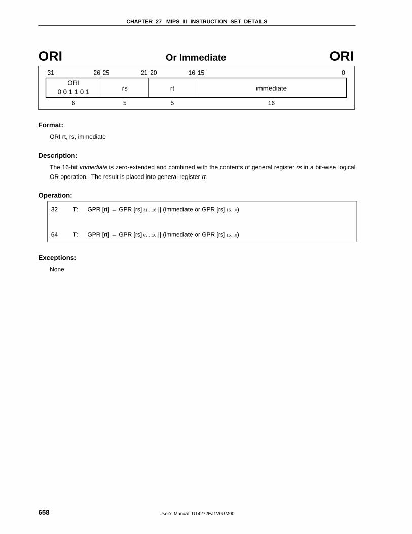
CHAPTER 27 MIPS III INSTRUCTION SET DETAILS
User’s Manual U14272EJ1V0UM00658
ORI Or Immediate ORI
ORI
31 26 25 21 20 16 15 0
rs0 0 1 1 0 1 rt immediate
6 5 5 16
Format:
ORI rt, rs, immediate
Description:
The 16-bit immediate is zero-extended and combined with the contents of general register rs in a bit-wise logical
OR operation. The result is placed into general register rt.
Operation:
32 T: GPR [rt] ← GPR [rs] 31…16 || (immediate or GPR [rs] 15…0)
64 T: GPR [rt] ← GPR [rs] 63…16 || (immediate or GPR [rs] 15…0)
Exceptions:
None
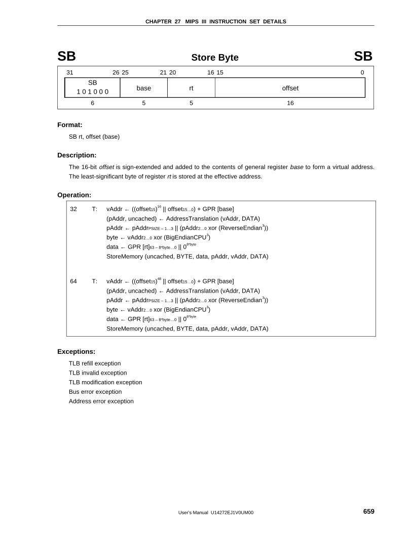
CHAPTER 27 MIPS III INSTRUCTION SET DETAILS
User’s Manual U14272EJ1V0UM00 659
SB Store Byte SB
SB
31 26 25 21 20 16 15 0
base1 0 1 0 0 0 rt offset
6 5 5 16
Format:
SB rt, offset (base)
Description:
The 16-bit offset is sign-extended and added to the contents of general register base to form a virtual address.
The least-significant byte of register rt is stored at the effective address.
Operation:
32 T: vAddr ← ((offset15)16 || offset15…0) + GPR [base]
(pAddr, uncached) ← AddressTranslation (vAddr, DATA)
pAddr ← pAddrPSIZE – 1…3 || (pAddr2…0 xor (ReverseEndian3))
byte ← vAddr2…0 xor (BigEndianCPU3)
data ← GPR [rt]63 – 8*byte…0 || 08*byte
StoreMemory (uncached, BYTE, data, pAddr, vAddr, DATA)
64 T: vAddr ← ((offset15)48 || offset15…0) + GPR [base]
(pAddr, uncached) ← AddressTranslation (vAddr, DATA)
pAddr ← pAddrPSIZE – 1…3 || (pAddr2…0 xor (ReverseEndian3))
byte ← vAddr2…0 xor (BigEndianCPU3)
data ← GPR [rt]63 – 8*byte…0 || 08*byte
StoreMemory (uncached, BYTE, data, pAddr, vAddr, DATA)
Exceptions:
TLB refill exception
TLB invalid exception
TLB modification exception
Bus error exception
Address error exception
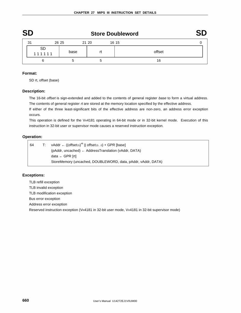
CHAPTER 27 MIPS III INSTRUCTION SET DETAILS
User’s Manual U14272EJ1V0UM00660
SD Store Doubleword SD
SD
31 26 25 21 20 16 15 0
base1 1 1 1 1 1 rt offset
6 5 5 16
Format:
SD rt, offset (base)
Description:
The 16-bit offset is sign-extended and added to the contents of general register base to form a virtual address.
The contents of general register rt are stored at the memory location specified by the effective address.
If either of the three least-significant bits of the effective address are non-zero, an address error exception
occurs.
This operation is defined for the VR4181 operating in 64-bit mode or in 32-bit kernel mode. Execution of this
instruction in 32-bit user or supervisor mode causes a reserved instruction exception.
Operation:
64 T: vAddr ← ((offset15)48 || offset15…0) + GPR [base]
(pAddr, uncached) ← AddressTranslation (vAddr, DATA)
data ← GPR [rt]
StoreMemory (uncached, DOUBLEWORD, data, pAddr, vAddr, DATA)
Exceptions:
TLB refill exception
TLB invalid exception
TLB modification exception
Bus error exception
Address error exception
Reserved instruction exception (VR4181 in 32-bit user mode, VR4181 in 32-bit supervisor mode)
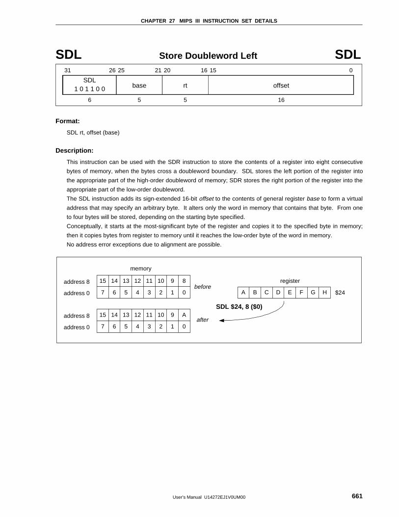
CHAPTER 27 MIPS III INSTRUCTION SET DETAILS
User’s Manual U14272EJ1V0UM00 661
SDL Store Doubleword Left SDL
SDL
31 26 25 21 20 16 15 0
base1 0 1 1 0 0 rt offset
6 5 5 16
Format:
SDL rt, offset (base)
Description:
This instruction can be used with the SDR instruction to store the contents of a register into eight consecutive
bytes of memory, when the bytes cross a doubleword boundary. SDL stores the left portion of the register into
the appropriate part of the high-order doubleword of memory; SDR stores the right portion of the register into the
appropriate part of the low-order doubleword.
The SDL instruction adds its sign-extended 16-bit offset to the contents of general register base to form a virtual
address that may specify an arbitrary byte. It alters only the word in memory that contains that byte. From one
to four bytes will be stored, depending on the starting byte specified.
Conceptually, it starts at the most-significant byte of the register and copies it to the specified byte in memory;
then it copies bytes from register to memory until it reaches the low-order byte of the word in memory.
No address error exceptions due to alignment are possible.
address 8
address 0
memory
before
after
$24
register
A B C D E F G H
15 14 13 12 11 10 9 8
7 6 5 4 3 2 1 0
SDL $24, 8 ($0)address 8
address 0
15 14 13 12 11 10 9 A
7 6 5 4 3 2 1 0
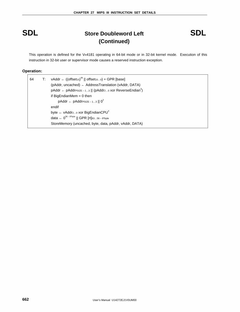
CHAPTER 27 MIPS III INSTRUCTION SET DETAILS
User’s Manual U14272EJ1V0UM00662
SDL Store Doubleword Left SDL(Continued)
This operation is defined for the VR4181 operating in 64-bit mode or in 32-bit kernel mode. Execution of this
instruction in 32-bit user or supervisor mode causes a reserved instruction exception.
Operation:
64 T: vAddr ← ((offset15)48 || offset15…0) + GPR [base]
(pAddr, uncached) ← AddressTranslation (vAddr, DATA)
pAddr ← pAddrPSIZE – 1…3 || (pAddr2…0 xor ReverseEndian3)
if BigEndianMem = 0 then
pAddr ← pAddrPSIZE – 1…3 || 03
endif
byte ← vAddr2…0 xor BigEndianCPU3
data ← 056 – 8*byte || GPR [rt]63…56 – 8*byte
StoreMemory (uncached, byte, data, pAddr, vAddr, DATA)
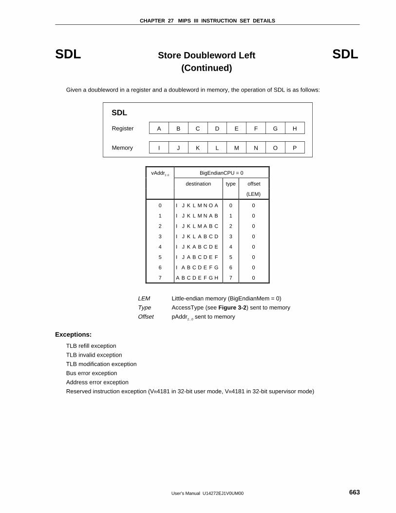
CHAPTER 27 MIPS III INSTRUCTION SET DETAILS
User’s Manual U14272EJ1V0UM00 663
SDL Store Doubleword Left SDL(Continued)
Given a doubleword in a register and a doubleword in memory, the operation of SDL is as follows:
B C D E F GA H
J K L M N OI P
Register
Memory
SDL
vAddr2..0 BigEndianCPU = 0
destination type offset
(LEM)
0
1
2
3
4
5
6
7
I J K L M N O A
I J K L M N A B
I J K L M A B C
I J K L A B C D
I J K A B C D E
I J A B C D E F
I A B C D E F G
A B C D E F G H
0
1
2
3
4
5
6
7
0
0
0
0
0
0
0
0
LEM Little-endian memory (BigEndianMem = 0)
Type AccessType (see Figure 3-2 ) sent to memory
Offset pAddr2...0 sent to memory
Exceptions:
TLB refill exception
TLB invalid exception
TLB modification exception
Bus error exception
Address error exception
Reserved instruction exception (VR4181 in 32-bit user mode, VR4181 in 32-bit supervisor mode)
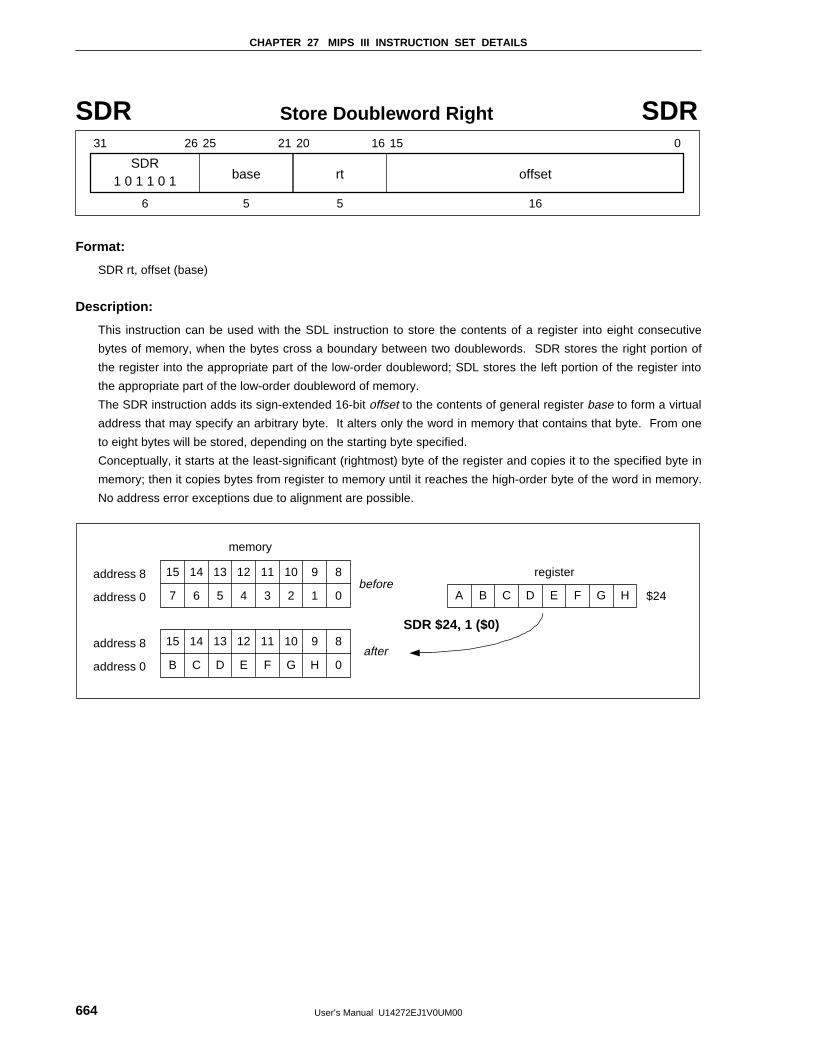
CHAPTER 27 MIPS III INSTRUCTION SET DETAILS
User’s Manual U14272EJ1V0UM00664
SDR Store Doubleword Right SDR
SDR
31 26 25 21 20 16 15 0
base1 0 1 1 0 1 rt offset
6 5 5 16
Format:
SDR rt, offset (base)
Description:
This instruction can be used with the SDL instruction to store the contents of a register into eight consecutive
bytes of memory, when the bytes cross a boundary between two doublewords. SDR stores the right portion of
the register into the appropriate part of the low-order doubleword; SDL stores the left portion of the register into
the appropriate part of the low-order doubleword of memory.
The SDR instruction adds its sign-extended 16-bit offset to the contents of general register base to form a virtual
address that may specify an arbitrary byte. It alters only the word in memory that contains that byte. From one
to eight bytes will be stored, depending on the starting byte specified.
Conceptually, it starts at the least-significant (rightmost) byte of the register and copies it to the specified byte in
memory; then it copies bytes from register to memory until it reaches the high-order byte of the word in memory.
No address error exceptions due to alignment are possible.
address 8
address 0
memory
before
after
$24
register
A B C D E F G H
15 14 13 12 11 10 9 8
7 6 5 4 3 2 1 0
SDR $24, 1 ($0)address 8
address 0
15 14 13 12 11 10 9 8
B C D E F G H 0
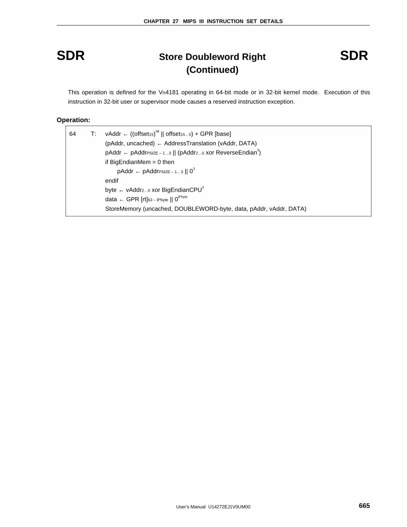
CHAPTER 27 MIPS III INSTRUCTION SET DETAILS
User’s Manual U14272EJ1V0UM00 665
SDR Store Doubleword Right SDR(Continued)
This operation is defined for the VR4181 operating in 64-bit mode or in 32-bit kernel mode. Execution of this
instruction in 32-bit user or supervisor mode causes a reserved instruction exception.
Operation:
64 T: vAddr ← ((offset15)48 || offset15…0) + GPR [base]
(pAddr, uncached) ← AddressTranslation (vAddr, DATA)
pAddr ← pAddrPSIZE – 1…3 || (pAddr2…0 xor ReverseEndian3)
if BigEndianMem = 0 then
pAddr ← pAddrPSIZE – 1…3 || 03
endif
byte ← vAddr2…0 xor BigEndianCPU3
data ← GPR [rt]63 – 8*byte || 08*byte
StoreMemory (uncached, DOUBLEWORD-byte, data, pAddr, vAddr, DATA)
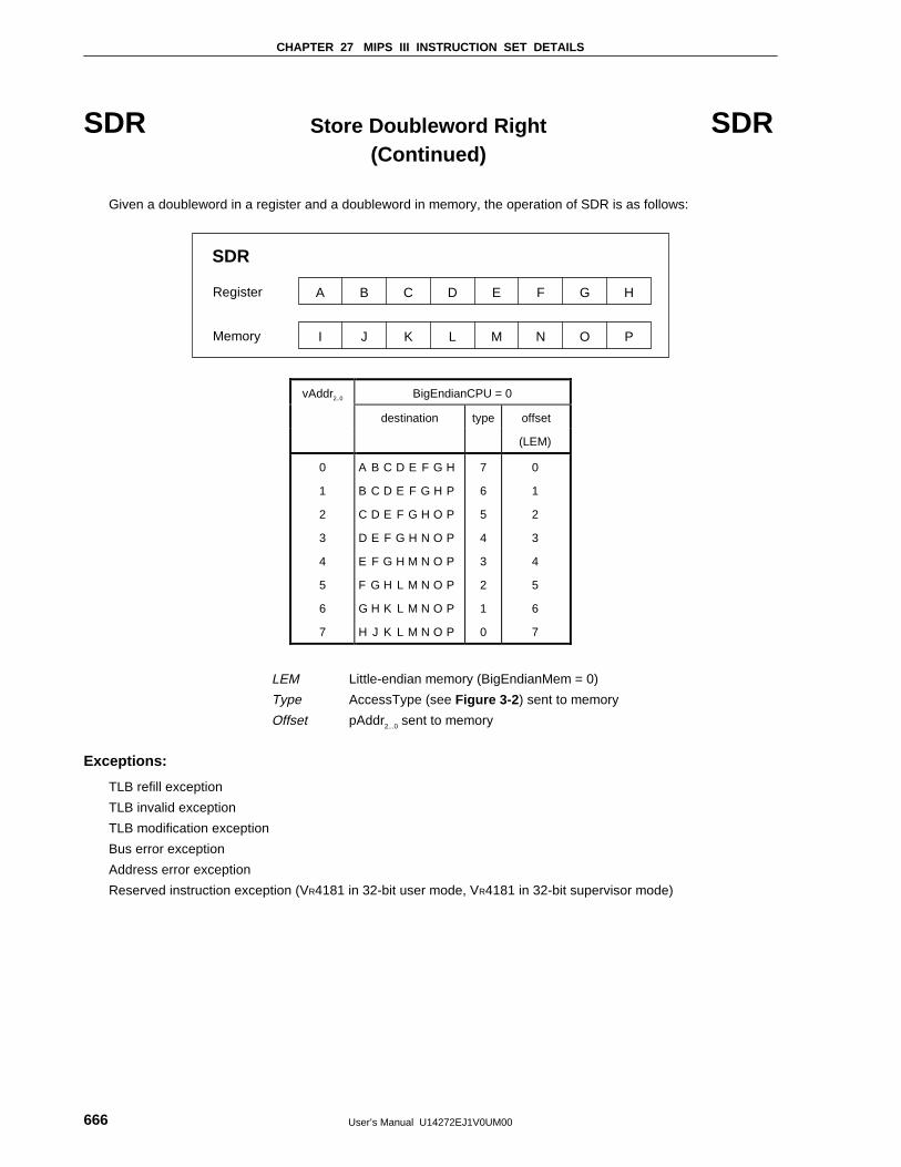
CHAPTER 27 MIPS III INSTRUCTION SET DETAILS
User’s Manual U14272EJ1V0UM00666
SDR Store Doubleword Right SDR(Continued)
Given a doubleword in a register and a doubleword in memory, the operation of SDR is as follows:
B C D E F GA H
J K L M N OI P
Register
Memory
SDR
vAddr2..0 BigEndianCPU = 0
destination type offset
(LEM)
0
1
2
3
4
5
6
7
A B C D E F G H
B C D E F G H P
C D E F G H O P
D E F G H N O P
E F G H M N O P
F G H L M N O P
G H K L M N O P
H J K L M N O P
7
6
5
4
3
2
1
0
0
1
2
3
4
5
6
7
LEM Little-endian memory (BigEndianMem = 0)
Type AccessType (see Figure 3-2 ) sent to memory
Offset pAddr2...0 sent to memory
Exceptions:
TLB refill exception
TLB invalid exception
TLB modification exception
Bus error exception
Address error exception
Reserved instruction exception (VR4181 in 32-bit user mode, VR4181 in 32-bit supervisor mode)
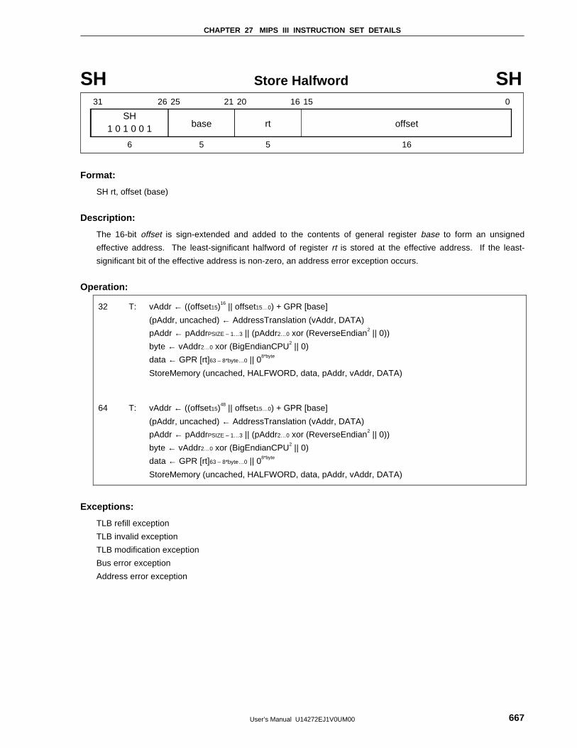
CHAPTER 27 MIPS III INSTRUCTION SET DETAILS
User’s Manual U14272EJ1V0UM00 667
SH Store Halfword SH
SH
31 26 25 21 20 16 15 0
base1 0 1 0 0 1 rt offset
6 5 5 16
Format:
SH rt, offset (base)
Description:
The 16-bit offset is sign-extended and added to the contents of general register base to form an unsigned
effective address. The least-significant halfword of register rt is stored at the effective address. If the least-
significant bit of the effective address is non-zero, an address error exception occurs.
Operation:
32 T: vAddr ← ((offset15)16 || offset15…0) + GPR [base]
(pAddr, uncached) ← AddressTranslation (vAddr, DATA)
pAddr ← pAddrPSIZE – 1…3 || (pAddr2…0 xor (ReverseEndian2 || 0))
byte ← vAddr2…0 xor (BigEndianCPU2 || 0)
data ← GPR [rt]63 – 8*byte…0 || 08*byte
StoreMemory (uncached, HALFWORD, data, pAddr, vAddr, DATA)
64 T: vAddr ← ((offset15)48 || offset15…0) + GPR [base]
(pAddr, uncached) ← AddressTranslation (vAddr, DATA)
pAddr ← pAddrPSIZE – 1…3 || (pAddr2…0 xor (ReverseEndian2 || 0))
byte ← vAddr2…0 xor (BigEndianCPU2 || 0)
data ← GPR [rt]63 – 8*byte…0 || 08*byte
StoreMemory (uncached, HALFWORD, data, pAddr, vAddr, DATA)
Exceptions:
TLB refill exception
TLB invalid exception
TLB modification exception
Bus error exception
Address error exception
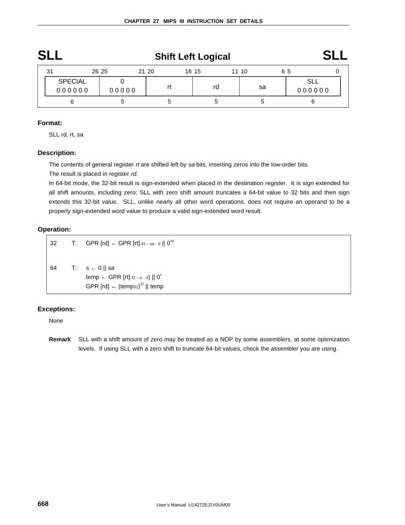
CHAPTER 27 MIPS III INSTRUCTION SET DETAILS
User’s Manual U14272EJ1V0UM00668
SLL Shift Left Logical SLL
SPECIAL
31 26 25 21 20 16 15 11 10 6 5 0
sa0 0 0 0 0 0 rt rd0
0 0 0 0 0SLL
0 0 0 0 0 0
6 5 5 5 5 6
Format:
SLL rd, rt, sa
Description:
The contents of general register rt are shifted left by sa bits, inserting zeros into the low-order bits.
The result is placed in register rd.
In 64-bit mode, the 32-bit result is sign-extended when placed in the destination register. It is sign extended for
all shift amounts, including zero; SLL with zero shift amount truncates a 64-bit value to 32 bits and then sign
extends this 32-bit value. SLL, unlike nearly all other word operations, does not require an operand to be a
properly sign-extended word value to produce a valid sign-extended word result.
Operation:
32 T: GPR [rd] ← GPR [rt] 31 – sa…0 || 0sa
64 T: s ← 0 || sa
temp ← GPR [rt] 31 – s…0) || 0s
GPR [rd] ← (temp31)32 || temp
Exceptions:
None
Remark SLL with a shift amount of zero may be treated as a NOP by some assemblers, at some optimization
levels. If using SLL with a zero shift to truncate 64-bit values, check the assembler you are using.
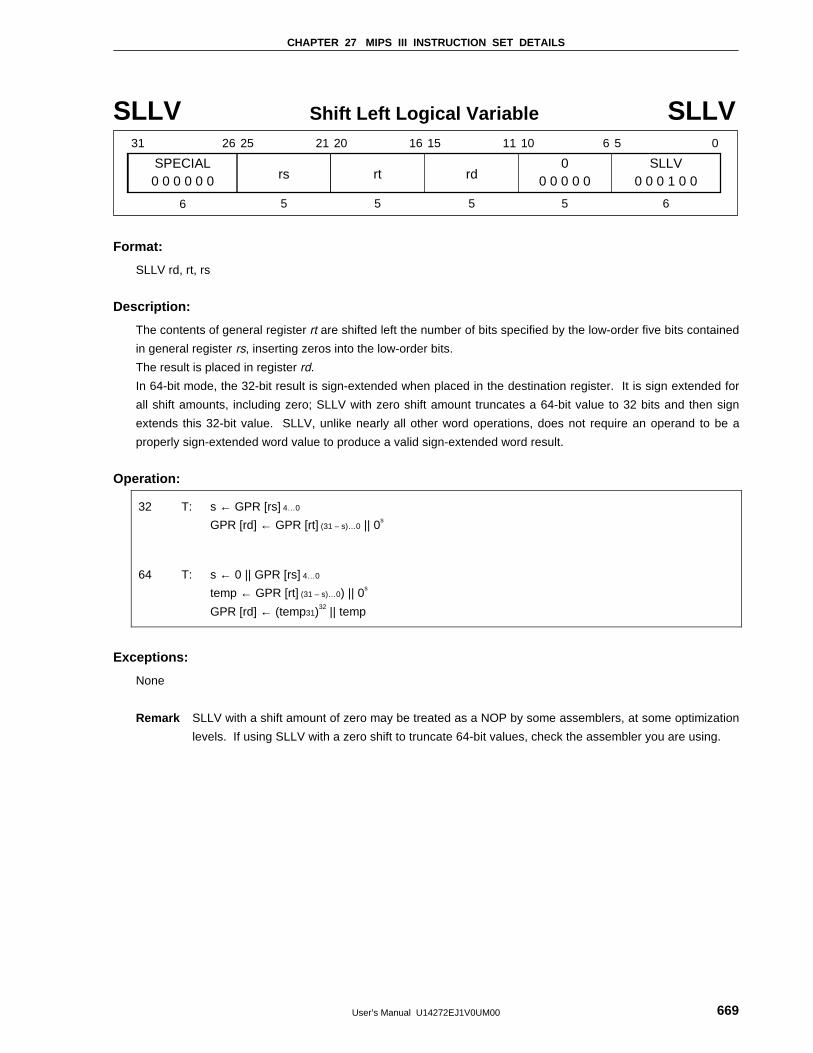
CHAPTER 27 MIPS III INSTRUCTION SET DETAILS
User’s Manual U14272EJ1V0UM00 669
SLLV Shift Left Logical Variable SLLV
SPECIAL
31 26 25 21 20 16 15 11 10 6 5 0
rs0 0 0 0 0 0 rt rd0
0 0 0 0 0SLLV
0 0 0 1 0 0
6 5 5 5 5 6
Format:
SLLV rd, rt, rs
Description:
The contents of general register rt are shifted left the number of bits specified by the low-order five bits contained
in general register rs, inserting zeros into the low-order bits.
The result is placed in register rd.
In 64-bit mode, the 32-bit result is sign-extended when placed in the destination register. It is sign extended for
all shift amounts, including zero; SLLV with zero shift amount truncates a 64-bit value to 32 bits and then sign
extends this 32-bit value. SLLV, unlike nearly all other word operations, does not require an operand to be a
properly sign-extended word value to produce a valid sign-extended word result.
Operation:
32 T: s ← GPR [rs] 4…0
GPR [rd] ← GPR [rt] (31 – s)…0 || 0s
64 T: s ← 0 || GPR [rs] 4…0
temp ← GPR [rt] (31 – s)…0) || 0s
GPR [rd] ← (temp31)32 || temp
Exceptions:
None
Remark SLLV with a shift amount of zero may be treated as a NOP by some assemblers, at some optimization
levels. If using SLLV with a zero shift to truncate 64-bit values, check the assembler you are using.
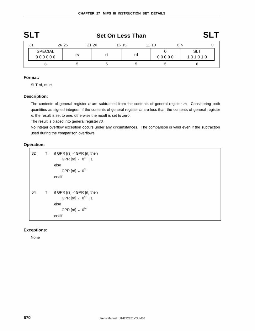
CHAPTER 27 MIPS III INSTRUCTION SET DETAILS
User’s Manual U14272EJ1V0UM00670
SLT Set On Less Than SLT
SPECIAL
31 26 25 21 20 16 15 11 10 6 5 0
rs0 0 0 0 0 0 rt rd0
0 0 0 0 0SLT
1 0 1 0 1 0
6 5 5 5 5 6
Format:
SLT rd, rs, rt
Description:
The contents of general register rt are subtracted from the contents of general register rs. Considering both
quantities as signed integers, if the contents of general register rs are less than the contents of general register
rt, the result is set to one; otherwise the result is set to zero.
The result is placed into general register rd.
No integer overflow exception occurs under any circumstances. The comparison is valid even if the subtraction
used during the comparison overflows.
Operation:
32 T: if GPR [rs] < GPR [rt] then
GPR [rd] ← 031 || 1
else
GPR [rd] ← 032
endif
64 T: if GPR [rs] < GPR [rt] then
GPR [rd] ← 063 || 1
else
GPR [rd] ← 064
endif
Exceptions:
None
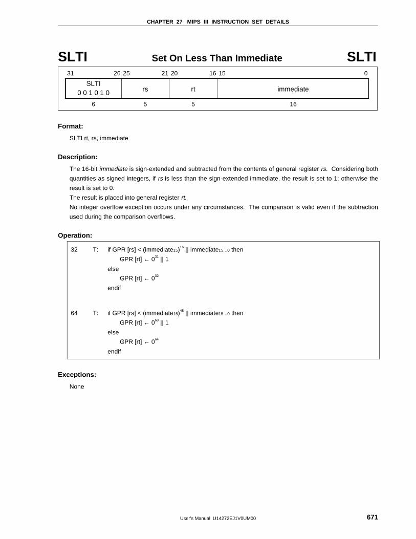
CHAPTER 27 MIPS III INSTRUCTION SET DETAILS
User’s Manual U14272EJ1V0UM00 671
SLTI Set On Less Than Immediate SLTI
SLTI
31 26 25 21 20 16 15 0
rs0 0 1 0 1 0 rt immediate
6 5 5 16
Format:
SLTI rt, rs, immediate
Description:
The 16-bit immediate is sign-extended and subtracted from the contents of general register rs. Considering both
quantities as signed integers, if rs is less than the sign-extended immediate, the result is set to 1; otherwise the
result is set to 0.
The result is placed into general register rt.
No integer overflow exception occurs under any circumstances. The comparison is valid even if the subtraction
used during the comparison overflows.
Operation:
32 T: if GPR [rs] < (immediate15)16 || immediate15…0 then
GPR [rt] ← 031 || 1
else
GPR [rt] ← 032
endif
64 T: if GPR [rs] < (immediate15)48 || immediate15…0 then
GPR [rt] ← 063 || 1
else
GPR [rt] ← 064
endif
Exceptions:
None
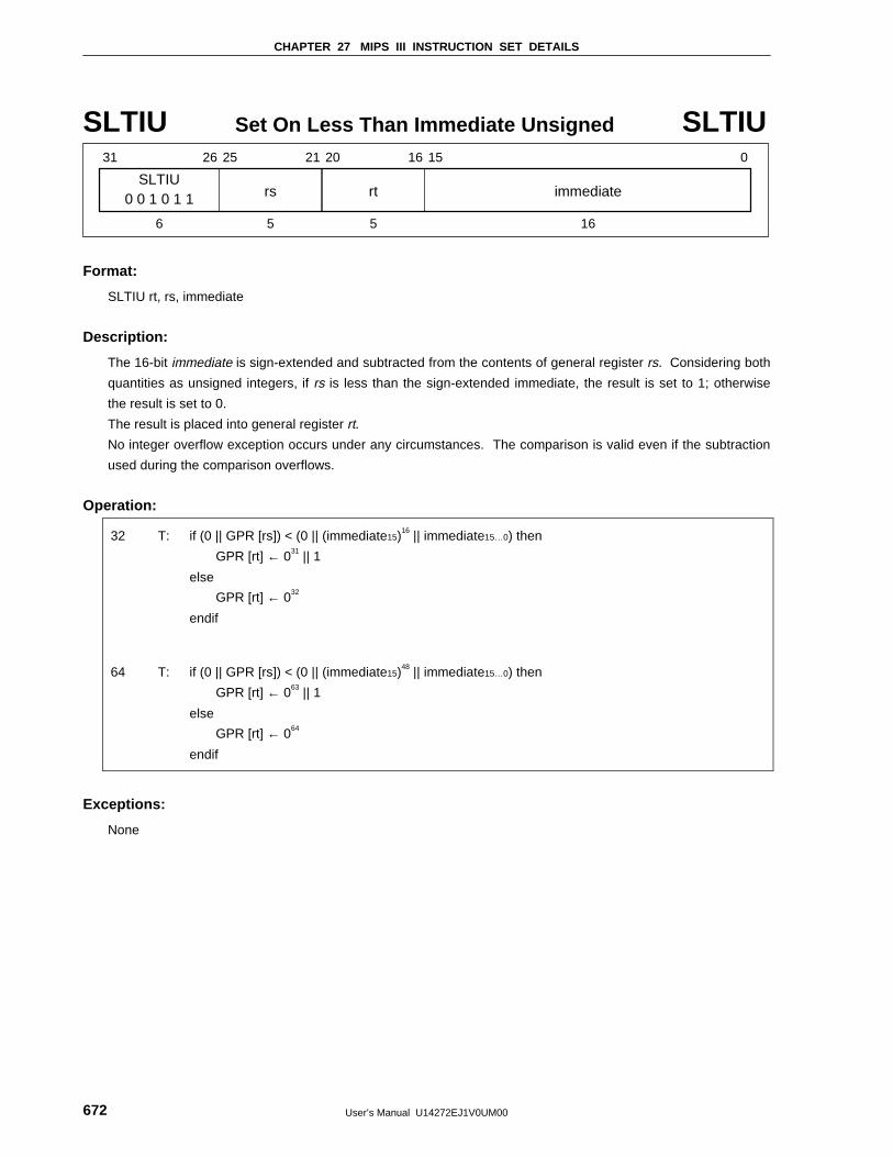
CHAPTER 27 MIPS III INSTRUCTION SET DETAILS
User’s Manual U14272EJ1V0UM00672
SLTIU Set On Less Than Immediate Unsigned SLTIU
SLTIU
31 26 25 21 20 16 15 0
rs0 0 1 0 1 1 rt immediate
6 5 5 16
Format:
SLTIU rt, rs, immediate
Description:
The 16-bit immediate is sign-extended and subtracted from the contents of general register rs. Considering both
quantities as unsigned integers, if rs is less than the sign-extended immediate, the result is set to 1; otherwise
the result is set to 0.
The result is placed into general register rt.
No integer overflow exception occurs under any circumstances. The comparison is valid even if the subtraction
used during the comparison overflows.
Operation:
32 T: if (0 || GPR [rs]) < (0 || (immediate15)16 || immediate15…0) then
GPR [rt] ← 031 || 1
else
GPR [rt] ← 032
endif
64 T: if (0 || GPR [rs]) < (0 || (immediate15)48 || immediate15…0) then
GPR [rt] ← 063 || 1
else
GPR [rt] ← 064
endif
Exceptions:
None
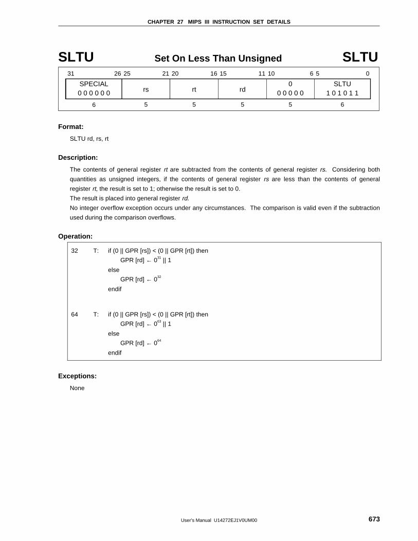
CHAPTER 27 MIPS III INSTRUCTION SET DETAILS
User’s Manual U14272EJ1V0UM00 673
SLTU Set On Less Than Unsigned SLTU
SPECIAL
31 26 25 21 20 16 15 11 10 6 5 0
rs0 0 0 0 0 0 rt rd0
0 0 0 0 0SLTU
1 0 1 0 1 1
6 5 5 5 5 6
Format:
SLTU rd, rs, rt
Description:
The contents of general register rt are subtracted from the contents of general register rs. Considering both
quantities as unsigned integers, if the contents of general register rs are less than the contents of general
register rt, the result is set to 1; otherwise the result is set to 0.
The result is placed into general register rd.
No integer overflow exception occurs under any circumstances. The comparison is valid even if the subtraction
used during the comparison overflows.
Operation:
32 T: if (0 || GPR [rs]) < (0 || GPR [rt]) then
GPR [rd] ← 031 || 1
else
GPR [rd] ← 032
endif
64 T: if (0 || GPR [rs]) < (0 || GPR [rt]) then
GPR [rd] ← 063 || 1
else
GPR [rd] ← 064
endif
Exceptions:
None
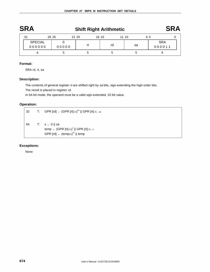
CHAPTER 27 MIPS III INSTRUCTION SET DETAILS
User’s Manual U14272EJ1V0UM00674
SRA Shift Right Arithmetic SRA
SPECIAL
31 26 25 21 20 16 15 11 10 6 5 0
sa0 0 0 0 0 0 rt rd0
0 0 0 0 0SRA
0 0 0 0 1 1
6 5 5 5 5 6
Format:
SRA rd, rt, sa
Description:
The contents of general register rt are shifted right by sa bits, sign-extending the high-order bits.
The result is placed in register rd.
In 64-bit mode, the operand must be a valid sign-extended, 32-bit value.
Operation:
32 T: GPR [rd] ← (GPR [rt] 31)sa || GPR [rt] 31…sa
64 T: s ← 0 || sa
temp ← (GPR [rt] 31)s || GPR [rt] 31…s
GPR [rd] ← (temp31)32 || temp
Exceptions:
None
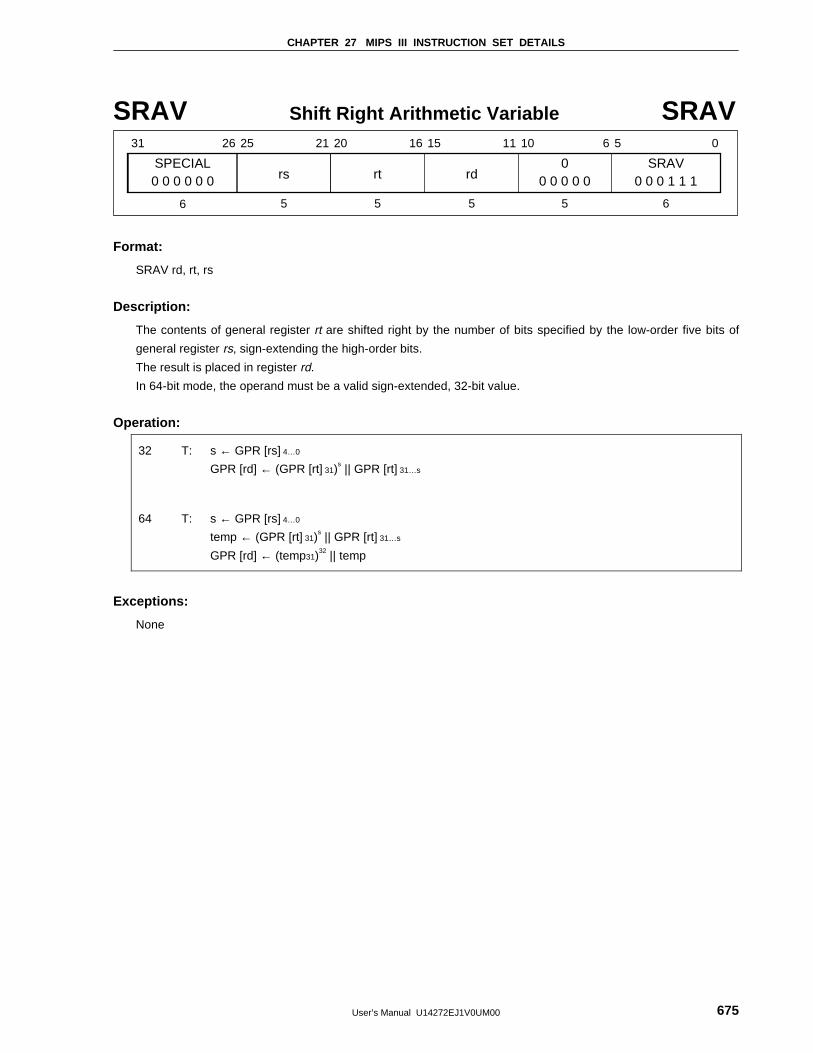
CHAPTER 27 MIPS III INSTRUCTION SET DETAILS
User’s Manual U14272EJ1V0UM00 675
SRAV Shift Right Arithmetic Variable SRAV
SPECIAL
31 26 25 21 20 16 15 11 10 6 5 0
rs0 0 0 0 0 0 rt rd0
0 0 0 0 0SRAV
0 0 0 1 1 1
6 5 5 5 5 6
Format:
SRAV rd, rt, rs
Description:
The contents of general register rt are shifted right by the number of bits specified by the low-order five bits of
general register rs, sign-extending the high-order bits.
The result is placed in register rd.
In 64-bit mode, the operand must be a valid sign-extended, 32-bit value.
Operation:
32 T: s ← GPR [rs] 4…0
GPR [rd] ← (GPR [rt] 31)s || GPR [rt] 31…s
64 T: s ← GPR [rs] 4…0
temp ← (GPR [rt] 31)s || GPR [rt] 31…s
GPR [rd] ← (temp31)32 || temp
Exceptions:
None
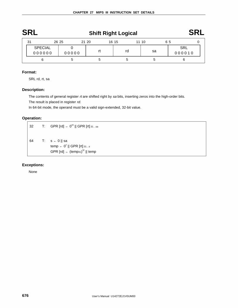
CHAPTER 27 MIPS III INSTRUCTION SET DETAILS
User’s Manual U14272EJ1V0UM00676
SRL Shift Right Logical SRL
SPECIAL
31 26 25 21 20 16 15 11 10 6 5 0
sa0 0 0 0 0 0 rt rd0
0 0 0 0 0SRL
0 0 0 0 1 0
6 5 5 5 5 6
Format:
SRL rd, rt, sa
Description:
The contents of general register rt are shifted right by sa bits, inserting zeros into the high-order bits.
The result is placed in register rd.
In 64-bit mode, the operand must be a valid sign-extended, 32-bit value.
Operation:
32 T: GPR [rd] ← 0sa || GPR [rt] 31…sa
64 T: s ← 0 || sa
temp ← 0s || GPR [rt] 31…s
GPR [rd] ← (temp31)32 || temp
Exceptions:
None
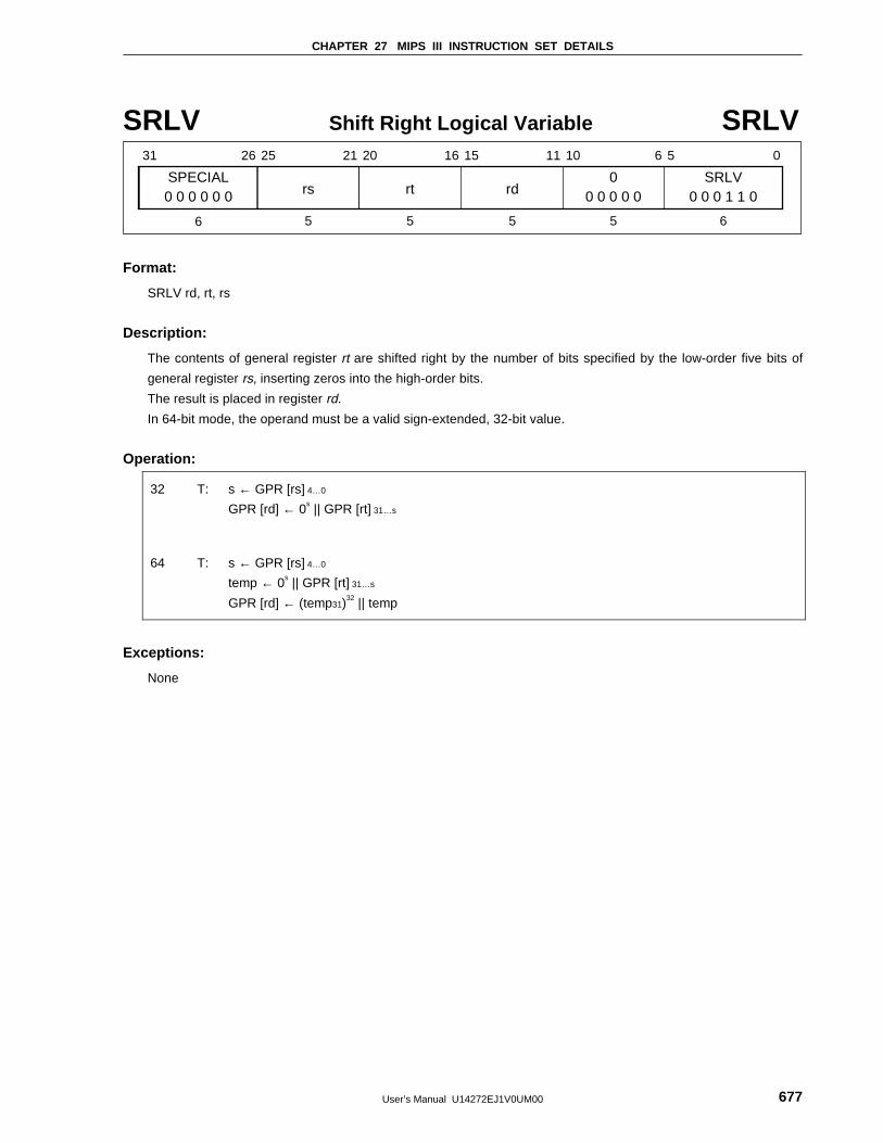
CHAPTER 27 MIPS III INSTRUCTION SET DETAILS
User’s Manual U14272EJ1V0UM00 677
SRLV Shift Right Logical Variable SRLV
SPECIAL
31 26 25 21 20 16 15 11 10 6 5 0
rs0 0 0 0 0 0 rt rd0
0 0 0 0 0SRLV
0 0 0 1 1 0
6 5 5 5 5 6
Format:
SRLV rd, rt, rs
Description:
The contents of general register rt are shifted right by the number of bits specified by the low-order five bits of
general register rs, inserting zeros into the high-order bits.
The result is placed in register rd.
In 64-bit mode, the operand must be a valid sign-extended, 32-bit value.
Operation:
32 T: s ← GPR [rs] 4…0
GPR [rd] ← 0s || GPR [rt] 31…s
64 T: s ← GPR [rs] 4…0
temp ← 0s || GPR [rt] 31…s
GPR [rd] ← (temp31)32 || temp
Exceptions:
None
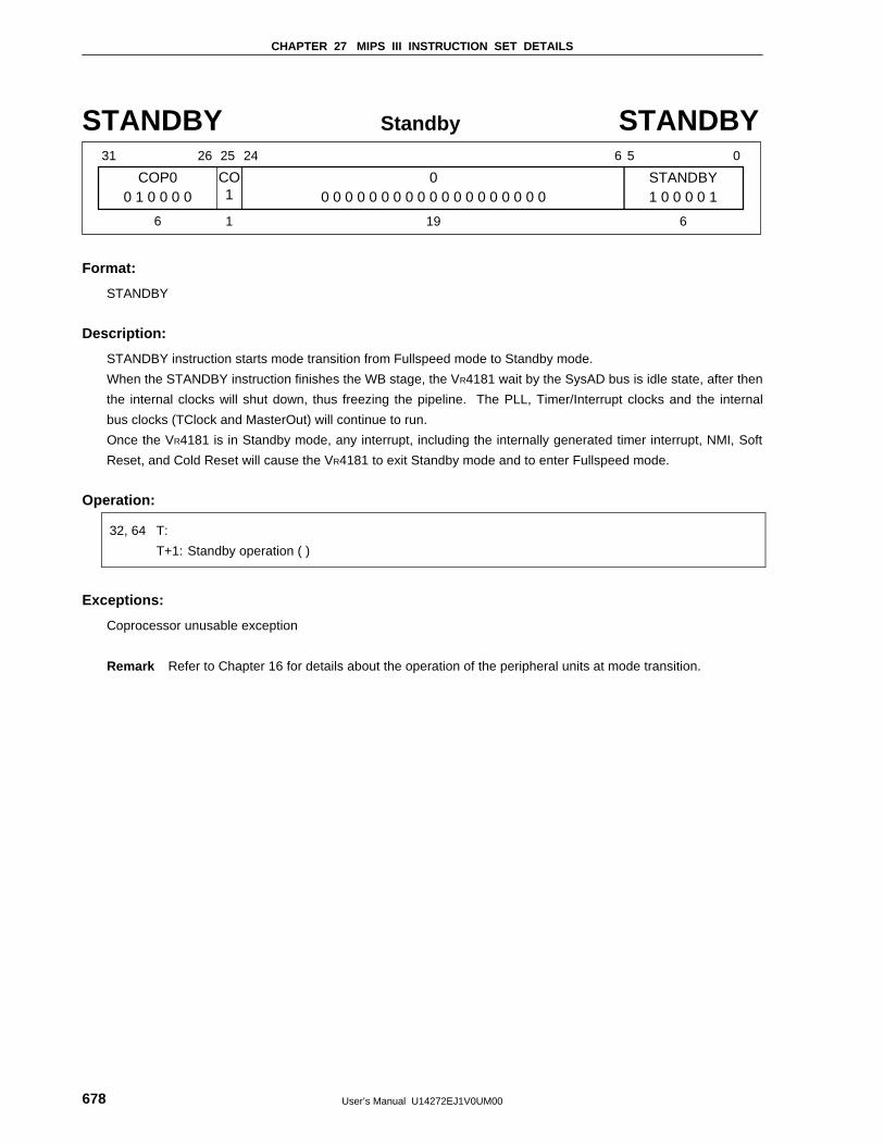
CHAPTER 27 MIPS III INSTRUCTION SET DETAILS
User’s Manual U14272EJ1V0UM00678
STANDBY Standby STANDBY
COP0
31 26 25 24 6 5 0
CO10 1 0 0 0 0
00 0 0 0 0 0 0 0 0 0 0 0 0 0 0 0 0 0 0
STANDBY1 0 0 0 0 1
6 1 19 6
Format:
STANDBY
Description:
STANDBY instruction starts mode transition from Fullspeed mode to Standby mode.
When the STANDBY instruction finishes the WB stage, the VR4181 wait by the SysAD bus is idle state, after then
the internal clocks will shut down, thus freezing the pipeline. The PLL, Timer/Interrupt clocks and the internal
bus clocks (TClock and MasterOut) will continue to run.
Once the VR4181 is in Standby mode, any interrupt, including the internally generated timer interrupt, NMI, Soft
Reset, and Cold Reset will cause the VR4181 to exit Standby mode and to enter Fullspeed mode.
Operation:
32, 64 T:
T+1: Standby operation ( )
Exceptions:
Coprocessor unusable exception
Remark Refer to Chapter 16 for details about the operation of the peripheral units at mode transition.
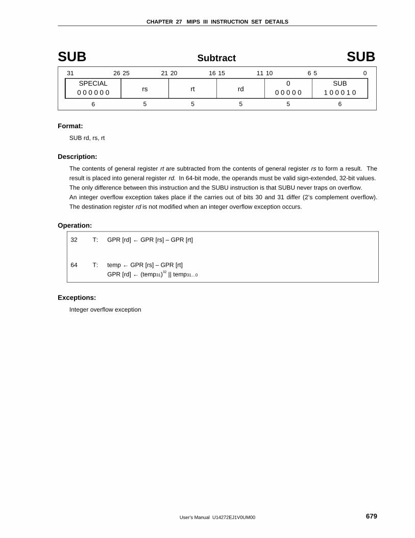
CHAPTER 27 MIPS III INSTRUCTION SET DETAILS
User’s Manual U14272EJ1V0UM00 679
SUB Subtract SUB
SPECIAL
31 26 25 21 20 16 15 11 10 6 5 0
rs0 0 0 0 0 0 rt rd0
0 0 0 0 0SUB
1 0 0 0 1 0
6 5 5 5 5 6
Format:
SUB rd, rs, rt
Description:
The contents of general register rt are subtracted from the contents of general register rs to form a result. The
result is placed into general register rd. In 64-bit mode, the operands must be valid sign-extended, 32-bit values.
The only difference between this instruction and the SUBU instruction is that SUBU never traps on overflow.
An integer overflow exception takes place if the carries out of bits 30 and 31 differ (2’s complement overflow).
The destination register rd is not modified when an integer overflow exception occurs.
Operation:
32 T: GPR [rd] ← GPR [rs] – GPR [rt]
64 T: temp ← GPR [rs] – GPR [rt]
GPR [rd] ← (temp31)32 || temp31…0
Exceptions:
Integer overflow exception
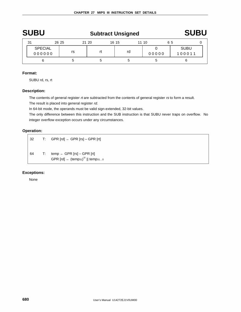
CHAPTER 27 MIPS III INSTRUCTION SET DETAILS
User’s Manual U14272EJ1V0UM00680
SUBU Subtract Unsigned SUBU
SPECIAL
31 26 25 21 20 16 15 11 10 6 5 0
rs0 0 0 0 0 0 rt rd0
0 0 0 0 0SUBU
1 0 0 0 1 1
6 5 5 5 5 6
Format:
SUBU rd, rs, rt
Description:
The contents of general register rt are subtracted from the contents of general register rs to form a result.
The result is placed into general register rd.
In 64-bit mode, the operands must be valid sign-extended, 32-bit values.
The only difference between this instruction and the SUB instruction is that SUBU never traps on overflow. No
integer overflow exception occurs under any circumstances.
Operation:
32 T: GPR [rd] ← GPR [rs] – GPR [rt]
64 T: temp ← GPR [rs] – GPR [rt]
GPR [rd] ← (temp31)32 || temp31…0
Exceptions:
None
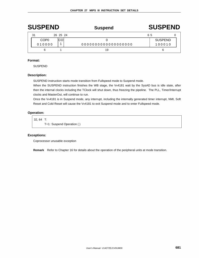
CHAPTER 27 MIPS III INSTRUCTION SET DETAILS
User’s Manual U14272EJ1V0UM00 681
SUSPEND Suspend SUSPEND
COP0
31 26 25 24 6 5 0
CO10 1 0 0 0 0
00 0 0 0 0 0 0 0 0 0 0 0 0 0 0 0 0 0 0
SUSPEND1 0 0 0 1 0
6 1 19 6
Format:
SUSPEND
Description:
SUSPEND instruction starts mode transition from Fullspeed mode to Suspend mode.
When the SUSPEND instruction finishes the WB stage, the VR4181 wait by the SysAD bus is idle state, after
then the internal clocks including the TClock will shut down, thus freezing the pipeline. The PLL, Timer/Interrupt
clocks and MasterOut, will continue to run.
Once the VR4181 is in Suspend mode, any interrupt, including the internally generated timer interrupt, NMI, Soft
Reset and Cold Reset will cause the VR4181 to exit Suspend mode and to enter Fullspeed mode.
Operation:
32, 64 T:
T+1: Suspend Operation ( )
Exceptions:
Coprocessor unusable exception
Remark Refer to Chapter 16 for details about the operation of the peripheral units at mode transition.
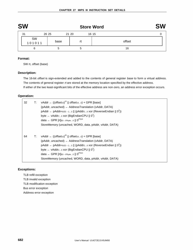
CHAPTER 27 MIPS III INSTRUCTION SET DETAILS
User’s Manual U14272EJ1V0UM00682
SW Store Word SW
SW
31 26 25 21 20 16 15 0
base1 0 1 0 1 1 rt offset
6 5 5 16
Format:
SW rt, offset (base)
Description:
The 16-bit offset is sign-extended and added to the contents of general register base to form a virtual address.
The contents of general register rt are stored at the memory location specified by the effective address.
If either of the two least-significant bits of the effective address are non-zero, an address error exception occurs.
Operation:
32 T: vAddr ← ((offset15)16 || offset15…0) + GPR [base]
(pAddr, uncached) ← AddressTranslation (vAddr, DATA)
pAddr ← pAddrPSIZE – 1…3 || (pAddr2…0 xor (ReverseEndian || 02))
byte ← vAddr2…0 xor (BigEndianCPU || 02)
data ← GPR [rt]63 – 8*byte…0 || 08*byte
StoreMemory (uncached, WORD, data, pAddr, vAddr, DATA)
64 T: vAddr ← ((offset15)48 || offset15…0) + GPR [base]
(pAddr, uncached) ← AddressTranslation (vAddr, DATA)
pAddr ← pAddrPSIZE – 1…3 || (pAddr2…0 xor (ReverseEndian || 02))
byte ← vAddr2…0 xor (BigEndianCPU || 02)
data ← GPR [rt]63 – 8*byte…0 || 08*byte
StoreMemory (uncached, WORD, data, pAddr, vAddr, DATA)
Exceptions:
TLB refill exception
TLB invalid exception
TLB modification exception
Bus error exception
Address error exception
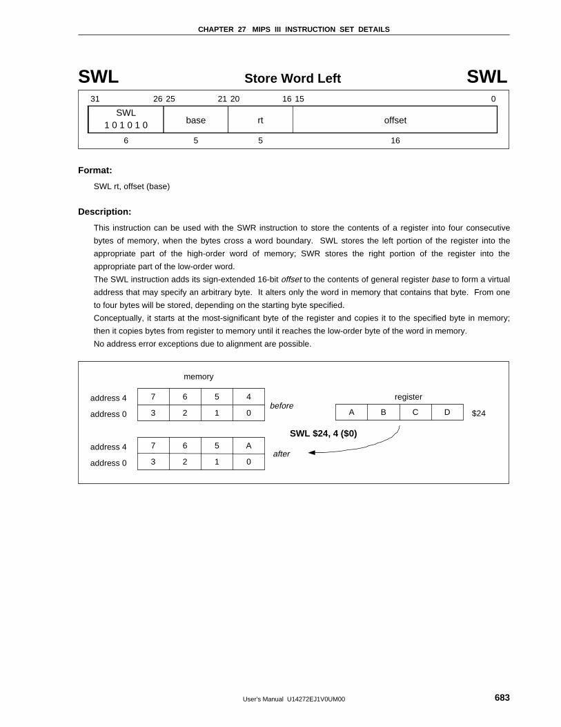
CHAPTER 27 MIPS III INSTRUCTION SET DETAILS
User’s Manual U14272EJ1V0UM00 683
SWL Store Word Left SWL
SWL
31 26 25 21 20 16 15 0
base1 0 1 0 1 0 rt offset
6 5 5 16
Format:
SWL rt, offset (base)
Description:
This instruction can be used with the SWR instruction to store the contents of a register into four consecutive
bytes of memory, when the bytes cross a word boundary. SWL stores the left portion of the register into the
appropriate part of the high-order word of memory; SWR stores the right portion of the register into the
appropriate part of the low-order word.
The SWL instruction adds its sign-extended 16-bit offset to the contents of general register base to form a virtual
address that may specify an arbitrary byte. It alters only the word in memory that contains that byte. From one
to four bytes will be stored, depending on the starting byte specified.
Conceptually, it starts at the most-significant byte of the register and copies it to the specified byte in memory;
then it copies bytes from register to memory until it reaches the low-order byte of the word in memory.
No address error exceptions due to alignment are possible.
address 4
address 0
memory
7before
after
$24
register
SWL $24, 4 ($0)
6 5 4
3 2 1 0 A B C D
address 4
address 0
7 6 5 A
3 2 1 0
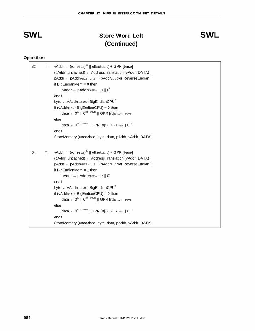
CHAPTER 27 MIPS III INSTRUCTION SET DETAILS
User’s Manual U14272EJ1V0UM00684
SWL Store Word Left SWL(Continued)
Operation:
32 T: vAddr ← ((offset15)16 || offset15…0) + GPR [base]
(pAddr, uncached) ← AddressTranslation (vAddr, DATA)
pAddr ← pAddrPSIZE – 1…3 || (pAddr2…0 xor ReverseEndian3)
if BigEndianMem = 0 then
pAddr ← pAddrPSIZE – 1…2 || 02
endif
byte ← vAddr1…0 xor BigEndianCPU2
if (vAddr2 xor BigEndianCPU) = 0 then
data ← 032 || 024 – 8*byte || GPR [rt]31…24 – 8*byte
else
data ← 024 – 8*byte || GPR [rt]31…24 – 8*byte || 032
endif
StoreMemory (uncached, byte, data, pAddr, vAddr, DATA)
64 T: vAddr ← ((offset15)48 || offset15…0) + GPR [base]
(pAddr, uncached) ← AddressTranslation (vAddr, DATA)
pAddr ← pAddrPSIZE – 1…3 || (pAddr2…0 xor ReverseEndian3)
if BigEndianMem = 1 then
pAddr ← pAddrPSIZE – 1…2 || 02
endif
byte ← vAddr1…0 xor BigEndianCPU2
if (vAddr2 xor BigEndianCPU) = 0 then
data ← 032 || 024 – 8*byte || GPR [rt]31…24 – 8*byte
else
data ← 024 – 8*byte || GPR [rt]31…24 – 8*byte || 032
endif
StoreMemory (uncached, byte, data, pAddr, vAddr, DATA)
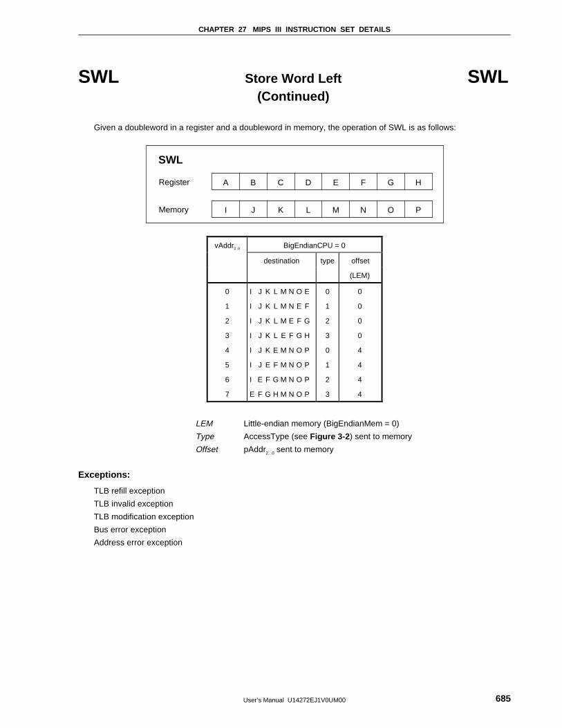
CHAPTER 27 MIPS III INSTRUCTION SET DETAILS
User’s Manual U14272EJ1V0UM00 685
SWL Store Word Left SWL(Continued)
Given a doubleword in a register and a doubleword in memory, the operation of SWL is as follows:
B C D E F GA H
J K L M N OI P
Register
Memory
SWL
vAddr2..0 BigEndianCPU = 0
destination type offset
(LEM)
0
1
2
3
4
5
6
7
I J K L M N O E
I J K L M N E F
I J K L M E F G
I J K L E F G H
I J K E M N O P
I J E F M N O P
I E F G M N O P
E F G H M N O P
0
1
2
3
0
1
2
3
0
0
0
0
4
4
4
4
LEM Little-endian memory (BigEndianMem = 0)
Type AccessType (see Figure 3-2 ) sent to memory
Offset pAddr2...0 sent to memory
Exceptions:
TLB refill exception
TLB invalid exception
TLB modification exception
Bus error exception
Address error exception
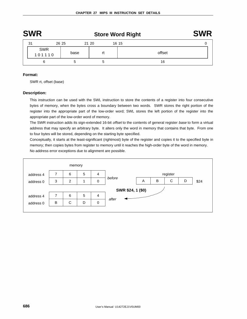
CHAPTER 27 MIPS III INSTRUCTION SET DETAILS
User’s Manual U14272EJ1V0UM00686
SWR Store Word Right SWR
SWR
31 26 25 21 20 16 15 0
base1 0 1 1 1 0 rt offset
6 5 5 16
Format:
SWR rt, offset (base)
Description:
This instruction can be used with the SWL instruction to store the contents of a register into four consecutive
bytes of memory, when the bytes cross a boundary between two words. SWR stores the right portion of the
register into the appropriate part of the low-order word; SWL stores the left portion of the register into the
appropriate part of the low-order word of memory.
The SWR instruction adds its sign-extended 16-bit offset to the contents of general register base to form a virtual
address that may specify an arbitrary byte. It alters only the word in memory that contains that byte. From one
to four bytes will be stored, depending on the starting byte specified.
Conceptually, it starts at the least-significant (rightmost) byte of the register and copies it to the specified byte in
memory; then copies bytes from register to memory until it reaches the high-order byte of the word in memory.
No address error exceptions due to alignment are possible.
address 4
address 0
memory
7before
after
$24
register
SWR $24, 1 ($0)
6 5 4
3 2 1 0 A B C D
address 4
address 0
7 6 5 4
B C D 0
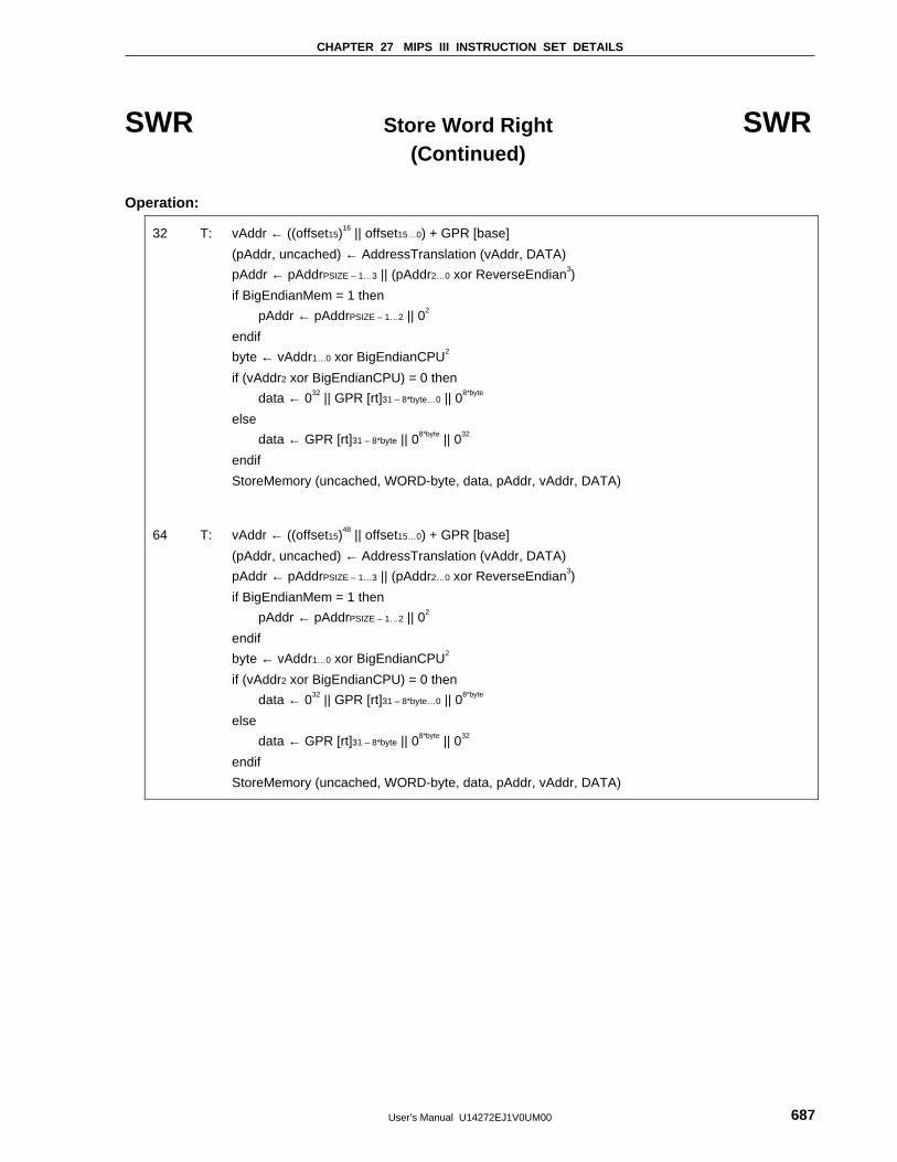
CHAPTER 27 MIPS III INSTRUCTION SET DETAILS
User’s Manual U14272EJ1V0UM00 687
SWR Store Word Right SWR(Continued)
Operation:
32 T: vAddr ← ((offset15)16 || offset15…0) + GPR [base]
(pAddr, uncached) ← AddressTranslation (vAddr, DATA)
pAddr ← pAddrPSIZE – 1…3 || (pAddr2…0 xor ReverseEndian3)
if BigEndianMem = 1 then
pAddr ← pAddrPSIZE – 1…2 || 02
endif
byte ← vAddr1…0 xor BigEndianCPU2
if (vAddr2 xor BigEndianCPU) = 0 then
data ← 032 || GPR [rt]31 – 8*byte…0 || 08*byte
else
data ← GPR [rt]31 – 8*byte || 08*byte || 032
endif
StoreMemory (uncached, WORD-byte, data, pAddr, vAddr, DATA)
64 T: vAddr ← ((offset15)48 || offset15…0) + GPR [base]
(pAddr, uncached) ← AddressTranslation (vAddr, DATA)
pAddr ← pAddrPSIZE – 1…3 || (pAddr2…0 xor ReverseEndian3)
if BigEndianMem = 1 then
pAddr ← pAddrPSIZE – 1…2 || 02
endif
byte ← vAddr1…0 xor BigEndianCPU2
if (vAddr2 xor BigEndianCPU) = 0 then
data ← 032 || GPR [rt]31 – 8*byte…0 || 08*byte
else
data ← GPR [rt]31 – 8*byte || 08*byte || 032
endif
StoreMemory (uncached, WORD-byte, data, pAddr, vAddr, DATA)
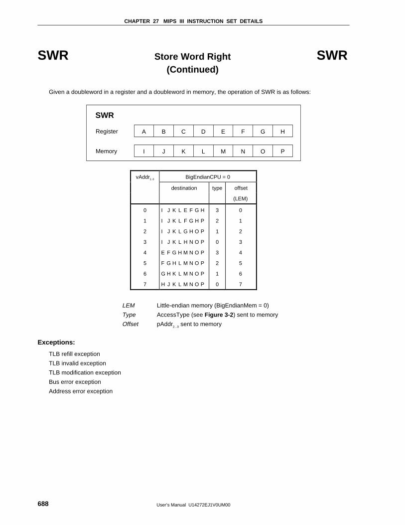
CHAPTER 27 MIPS III INSTRUCTION SET DETAILS
User’s Manual U14272EJ1V0UM00688
SWR Store Word Right SWR(Continued)
Given a doubleword in a register and a doubleword in memory, the operation of SWR is as follows:
B C D E F GA H
J K L M N OI P
Register
Memory
SWR
vAddr2..0 BigEndianCPU = 0
destination type offset
(LEM)
0
1
2
3
4
5
6
7
I J K L E F G H
I J K L F G H P
I J K L G H O P
I J K L H N O P
E F G H M N O P
F G H L M N O P
G H K L M N O P
H J K L M N O P
3
2
1
0
3
2
1
0
0
1
2
3
4
5
6
7
LEM Little-endian memory (BigEndianMem = 0)
Type AccessType (see Figure 3-2 ) sent to memory
Offset pAddr2...0 sent to memory
Exceptions:
TLB refill exception
TLB invalid exception
TLB modification exception
Bus error exception
Address error exception
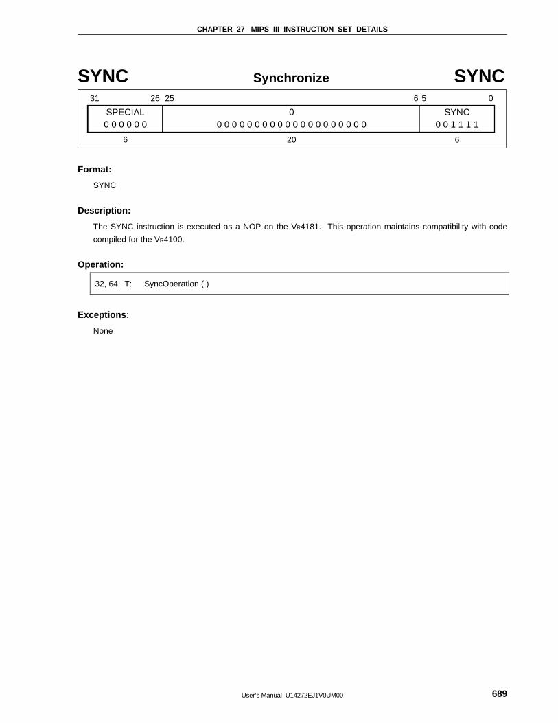
CHAPTER 27 MIPS III INSTRUCTION SET DETAILS
User’s Manual U14272EJ1V0UM00 689
SYNC Synchronize SYNC
SPECIAL
31 26 25 6 5 0
0 0 0 0 0 00
0 0 0 0 0 0 0 0 0 0 0 0 0 0 0 0 0 0 0 0SYNC
0 0 1 1 1 1
6 20 6
Format:
SYNC
Description:
The SYNC instruction is executed as a NOP on the VR4181. This operation maintains compatibility with code
compiled for the VR4100.
Operation:
32, 64 T: SyncOperation ( )
Exceptions:
None
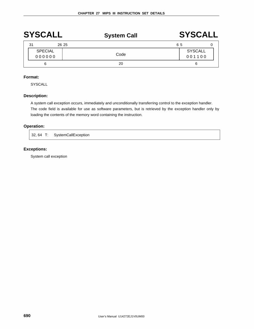
CHAPTER 27 MIPS III INSTRUCTION SET DETAILS
User’s Manual U14272EJ1V0UM00690
SYSCALL System Call SYSCALL
SPECIAL
31 26 25 6 5 0
Code0 0 0 0 0 0SYSCALL0 0 1 1 0 0
6 20 6
Format:
SYSCALL
Description:
A system call exception occurs, immediately and unconditionally transferring control to the exception handler.
The code field is available for use as software parameters, but is retrieved by the exception handler only by
loading the contents of the memory word containing the instruction.
Operation:
32, 64 T: SystemCallException
Exceptions:
System call exception
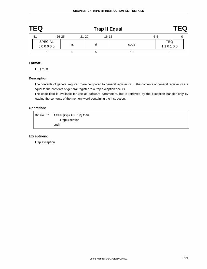
CHAPTER 27 MIPS III INSTRUCTION SET DETAILS
User’s Manual U14272EJ1V0UM00 691
TEQ Trap If Equal TEQ
SPECIAL
31 26 25 21 20 16 15 6 5 0
rs0 0 0 0 0 0 rtTEQ
1 1 0 1 0 0
6 5 5 10 6
code
Format:
TEQ rs, rt
Description:
The contents of general register rt are compared to general register rs. If the contents of general register rs are
equal to the contents of general register rt, a trap exception occurs.
The code field is available for use as software parameters, but is retrieved by the exception handler only by
loading the contents of the memory word containing the instruction.
Operation:
32, 64 T: if GPR [rs] = GPR [rt] then
TrapException
endif
Exceptions:
Trap exception
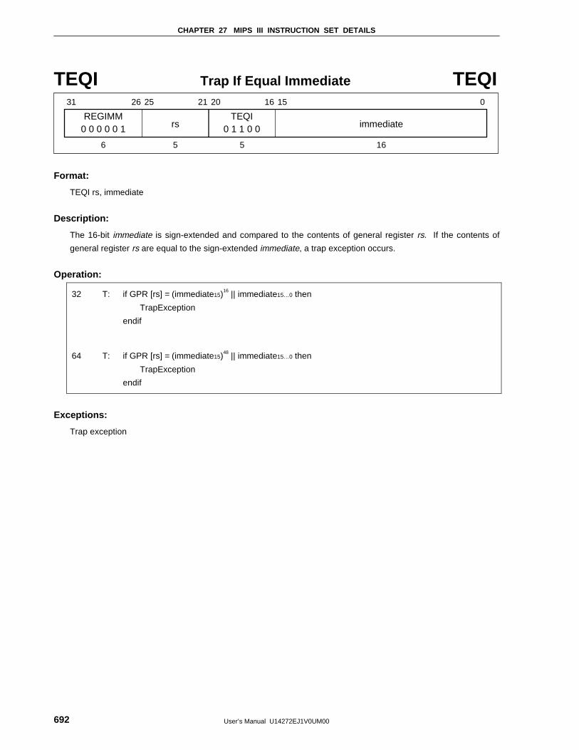
CHAPTER 27 MIPS III INSTRUCTION SET DETAILS
User’s Manual U14272EJ1V0UM00692
TEQI Trap If Equal Immediate TEQI
REGIMM
31 26 25 21 20 16 15 0
rs0 0 0 0 0 1 immediate
6 5 5 16
TEQI0 1 1 0 0
Format:
TEQI rs, immediate
Description:
The 16-bit immediate is sign-extended and compared to the contents of general register rs. If the contents of
general register rs are equal to the sign-extended immediate, a trap exception occurs.
Operation:
32 T: if GPR [rs] = (immediate15)16 || immediate15…0 then
TrapException
endif
64 T: if GPR [rs] = (immediate15)48 || immediate15…0 then
TrapException
endif
Exceptions:
Trap exception
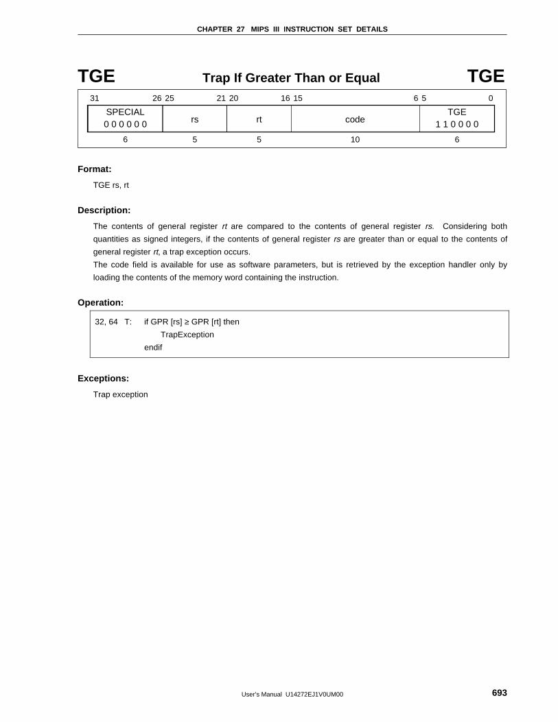
CHAPTER 27 MIPS III INSTRUCTION SET DETAILS
User’s Manual U14272EJ1V0UM00 693
TGE Trap If Greater Than or Equal TGE
SPECIAL
31 26 25 21 20 16 15 6 5 0
rs0 0 0 0 0 0 rtTGE
1 1 0 0 0 0
6 5 5 10 6
code
Format:
TGE rs, rt
Description:
The contents of general register rt are compared to the contents of general register rs. Considering both
quantities as signed integers, if the contents of general register rs are greater than or equal to the contents of
general register rt, a trap exception occurs.
The code field is available for use as software parameters, but is retrieved by the exception handler only by
loading the contents of the memory word containing the instruction.
Operation:
32, 64 T: if GPR [rs] ≥ GPR [rt] then
TrapException
endif
Exceptions:
Trap exception
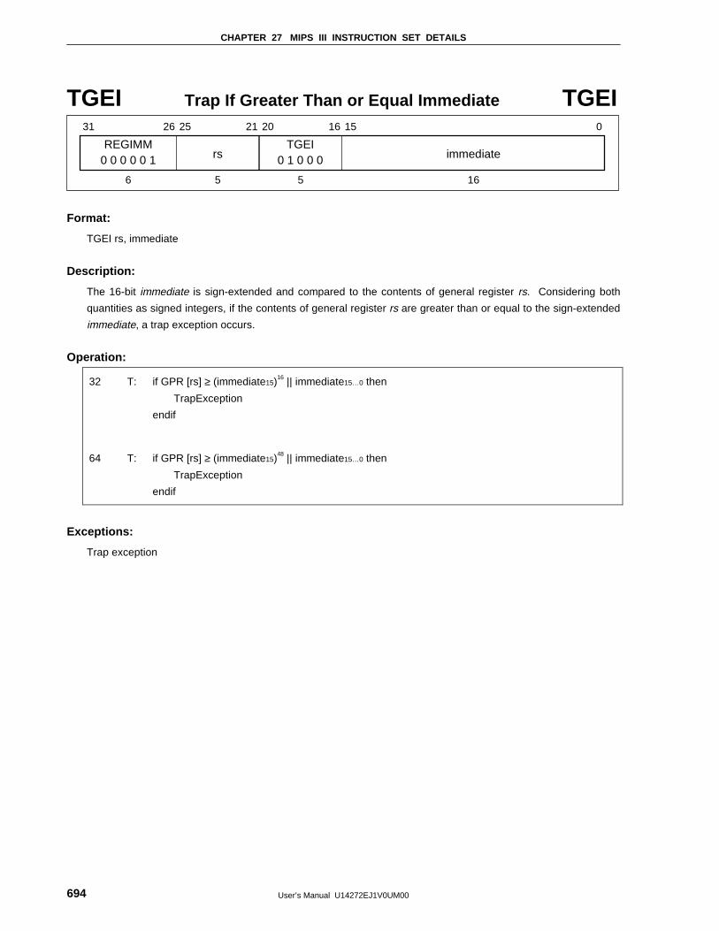
CHAPTER 27 MIPS III INSTRUCTION SET DETAILS
User’s Manual U14272EJ1V0UM00694
TGEI Trap If Greater Than or Equal Immediate TGEI
REGIMM
31 26 25 21 20 16 15 0
rs0 0 0 0 0 1 immediate
6 5 5 16
TGEI0 1 0 0 0
Format:
TGEI rs, immediate
Description:
The 16-bit immediate is sign-extended and compared to the contents of general register rs. Considering both
quantities as signed integers, if the contents of general register rs are greater than or equal to the sign-extended
immediate, a trap exception occurs.
Operation:
32 T: if GPR [rs] ≥ (immediate15)16 || immediate15…0 then
TrapException
endif
64 T: if GPR [rs] ≥ (immediate15)48 || immediate15…0 then
TrapException
endif
Exceptions:
Trap exception
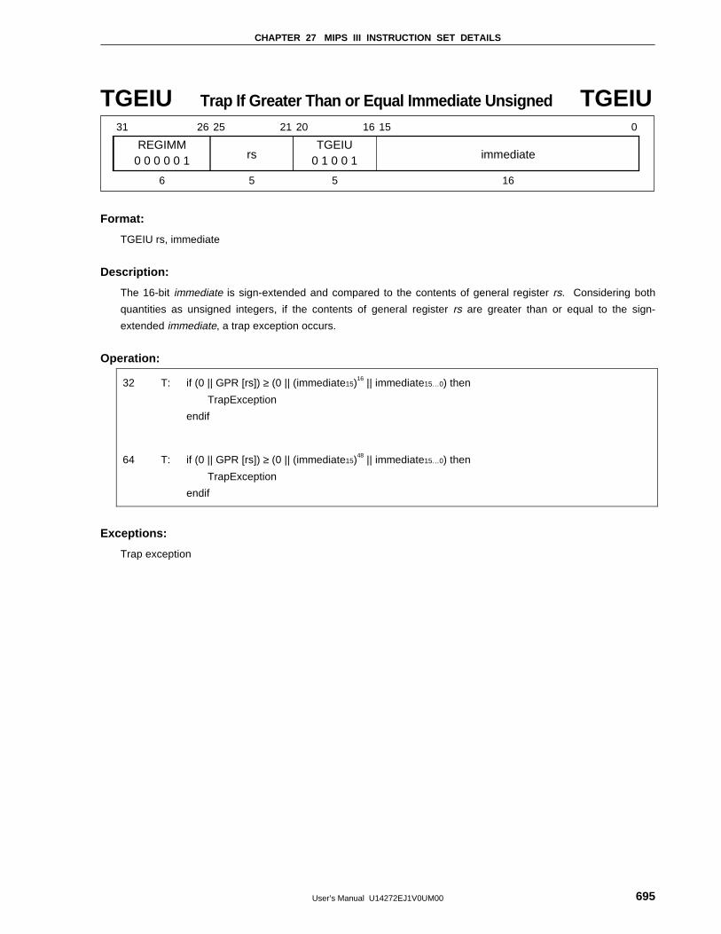
CHAPTER 27 MIPS III INSTRUCTION SET DETAILS
User’s Manual U14272EJ1V0UM00 695
TGEIU Trap If Greater Than or Equal Immediate Unsigned TGEIU
REGIMM
31 26 25 21 20 16 15 0
rs0 0 0 0 0 1 immediate
6 5 5 16
TGEIU0 1 0 0 1
Format:
TGEIU rs, immediate
Description:
The 16-bit immediate is sign-extended and compared to the contents of general register rs. Considering both
quantities as unsigned integers, if the contents of general register rs are greater than or equal to the sign-
extended immediate, a trap exception occurs.
Operation:
32 T: if (0 || GPR [rs]) ≥ (0 || (immediate15)16 || immediate15…0) then
TrapException
endif
64 T: if (0 || GPR [rs]) ≥ (0 || (immediate15)48 || immediate15…0) then
TrapException
endif
Exceptions:
Trap exception
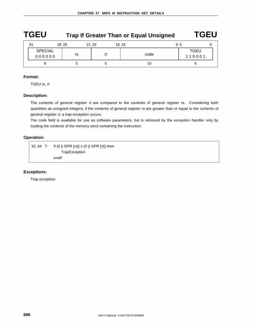
CHAPTER 27 MIPS III INSTRUCTION SET DETAILS
User’s Manual U14272EJ1V0UM00696
TGEU Trap If Greater Than or Equal Unsigned TGEU
SPECIAL
31 26 25 21 20 16 15 6 5 0
rs0 0 0 0 0 0 rtTGEU
1 1 0 0 0 1
6 5 5 10 6
code
Format:
TGEU rs, rt
Description:
The contents of general register rt are compared to the contents of general register rs. Considering both
quantities as unsigned integers, if the contents of general register rs are greater than or equal to the contents of
general register rt, a trap exception occurs.
The code field is available for use as software parameters, but is retrieved by the exception handler only by
loading the contents of the memory word containing the instruction.
Operation:
32, 64 T: if (0 || GPR [rs]) ≥ (0 || GPR [rt]) then
TrapException
endif
Exceptions:
Trap exception
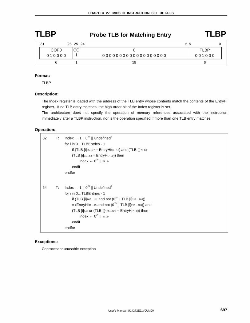
CHAPTER 27 MIPS III INSTRUCTION SET DETAILS
User’s Manual U14272EJ1V0UM00 697
TLBP Probe TLB for Matching Entry TLBP
COP0
31 26 25 24 6 5 0
CO10 1 0 0 0 0
00 0 0 0 0 0 0 0 0 0 0 0 0 0 0 0 0 0 0
TLBP0 0 1 0 0 0
6 1 19 6
Format:
TLBP
Description:
The Index register is loaded with the address of the TLB entry whose contents match the contents of the EntryHi
register. If no TLB entry matches, the high-order bit of the Index register is set.
The architecture does not specify the operation of memory references associated with the instruction
immediately after a TLBP instruction, nor is the operation specified if more than one TLB entry matches.
Operation:
32 T: Index ← 1 || 025 || Undefined6
for i in 0…TLBEntries - 1
if (TLB [i]95…77 = EntryHi31…13) and (TLB [i]76 or
(TLB [i]71…64 = EntryHi7…0)) then
Index ← 026 || i5…0
endif
endfor
64 T: Index ← 1 || 025 || Undefined6
for i in 0…TLBEntries - 1
if (TLB [i]167…141 and not (015 || TLB [i]216…205))
= (EntryHi39…13 and not (015 || TLB [i]216…205)) and
(TLB [i]140 or (TLB [i]135…126 = EntryHi7…0)) then
Index ← 026 || i5…0
endif
endfor
Exceptions:
Coprocessor unusable exception
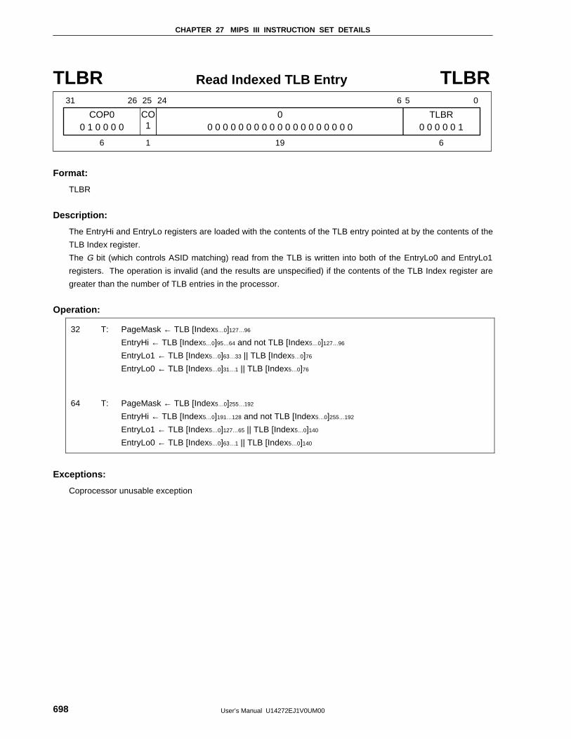
CHAPTER 27 MIPS III INSTRUCTION SET DETAILS
User’s Manual U14272EJ1V0UM00698
TLBR Read Indexed TLB Entry TLBR
COP0
31 26 25 24 6 5 0
CO10 1 0 0 0 0
00 0 0 0 0 0 0 0 0 0 0 0 0 0 0 0 0 0 0
TLBR0 0 0 0 0 1
6 1 19 6
Format:
TLBR
Description:
The EntryHi and EntryLo registers are loaded with the contents of the TLB entry pointed at by the contents of the
TLB Index register.
The G bit (which controls ASID matching) read from the TLB is written into both of the EntryLo0 and EntryLo1
registers. The operation is invalid (and the results are unspecified) if the contents of the TLB Index register are
greater than the number of TLB entries in the processor.
Operation:
32 T: PageMask ← TLB [Index5…0]127…96
EntryHi ← TLB [Index5…0]95…64 and not TLB [Index5…0]127…96
EntryLo1 ← TLB [Index5…0]63…33 || TLB [Index5…0]76
EntryLo0 ← TLB [Index5…0]31…1 || TLB [Index5…0]76
64 T: PageMask ← TLB [Index5…0]255…192
EntryHi ← TLB [Index5…0]191…128 and not TLB [Index5…0]255…192
EntryLo1 ← TLB [Index5…0]127…65 || TLB [Index5…0]140
EntryLo0 ← TLB [Index5…0]63…1 || TLB [Index5…0]140
Exceptions:
Coprocessor unusable exception
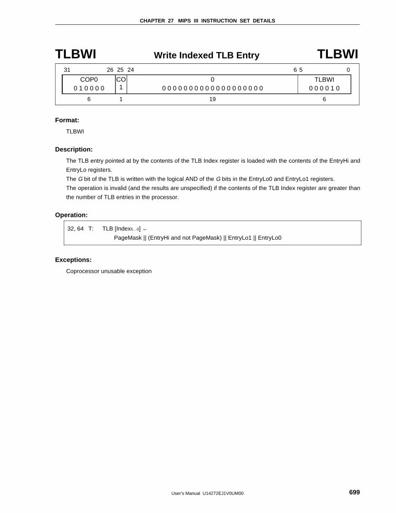
CHAPTER 27 MIPS III INSTRUCTION SET DETAILS
User’s Manual U14272EJ1V0UM00 699
TLBWI Write Indexed TLB Entry TLBWI
COP0
31 26 25 24 6 5 0
CO10 1 0 0 0 0
00 0 0 0 0 0 0 0 0 0 0 0 0 0 0 0 0 0 0
TLBWI0 0 0 0 1 0
6 1 19 6
Format:
TLBWI
Description:
The TLB entry pointed at by the contents of the TLB Index register is loaded with the contents of the EntryHi and
EntryLo registers.
The G bit of the TLB is written with the logical AND of the G bits in the EntryLo0 and EntryLo1 registers.
The operation is invalid (and the results are unspecified) if the contents of the TLB Index register are greater than
the number of TLB entries in the processor.
Operation:
32, 64 T: TLB [Index5…0] ←PageMask || (EntryHi and not PageMask) || EntryLo1 || EntryLo0
Exceptions:
Coprocessor unusable exception
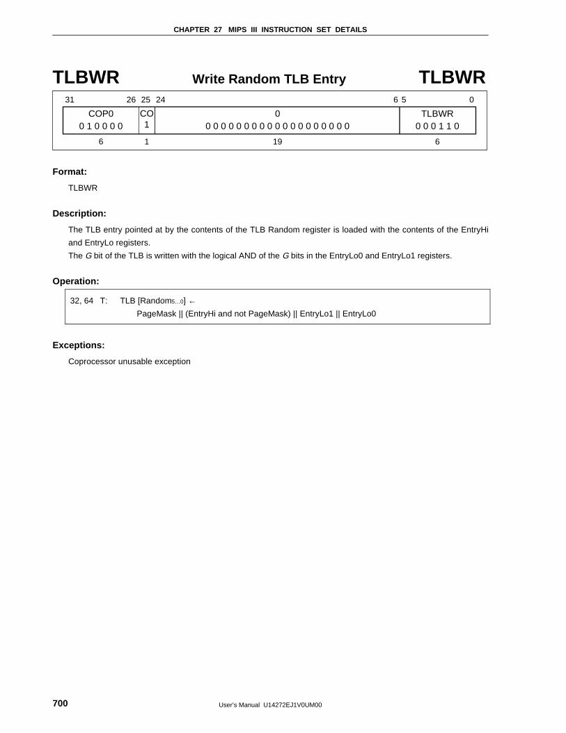
CHAPTER 27 MIPS III INSTRUCTION SET DETAILS
User’s Manual U14272EJ1V0UM00700
TLBWR Write Random TLB Entry TLBWR
COP0
31 26 25 24 6 5 0
CO10 1 0 0 0 0
00 0 0 0 0 0 0 0 0 0 0 0 0 0 0 0 0 0 0
TLBWR0 0 0 1 1 0
6 1 19 6
Format:
TLBWR
Description:
The TLB entry pointed at by the contents of the TLB Random register is loaded with the contents of the EntryHi
and EntryLo registers.
The G bit of the TLB is written with the logical AND of the G bits in the EntryLo0 and EntryLo1 registers.
Operation:
32, 64 T: TLB [Random5…0] ←PageMask || (EntryHi and not PageMask) || EntryLo1 || EntryLo0
Exceptions:
Coprocessor unusable exception
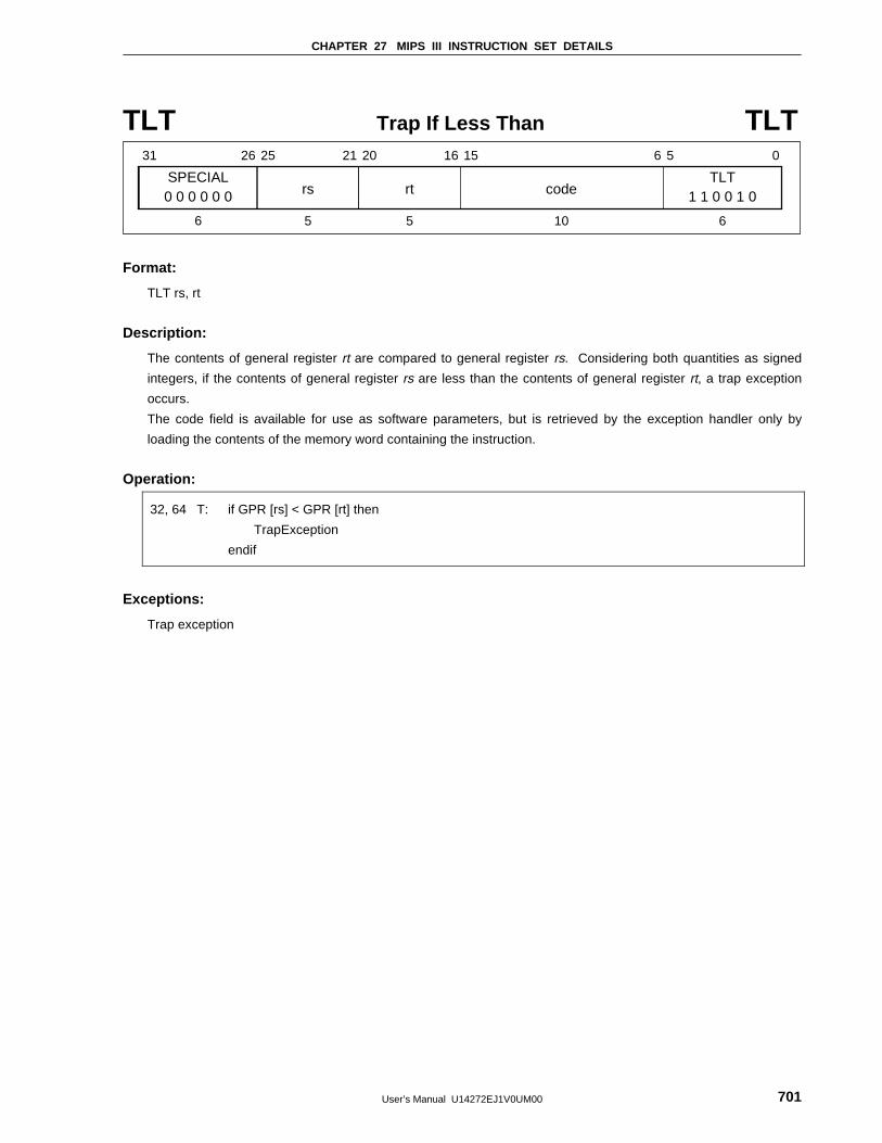
CHAPTER 27 MIPS III INSTRUCTION SET DETAILS
User’s Manual U14272EJ1V0UM00 701
TLT Trap If Less Than TLT
SPECIAL
31 26 25 21 20 16 15 6 5 0
rs0 0 0 0 0 0 rtTLT
1 1 0 0 1 0
6 5 5 10 6
code
Format:
TLT rs, rt
Description:
The contents of general register rt are compared to general register rs. Considering both quantities as signed
integers, if the contents of general register rs are less than the contents of general register rt, a trap exception
occurs.
The code field is available for use as software parameters, but is retrieved by the exception handler only by
loading the contents of the memory word containing the instruction.
Operation:
32, 64 T: if GPR [rs] < GPR [rt] then
TrapException
endif
Exceptions:
Trap exception
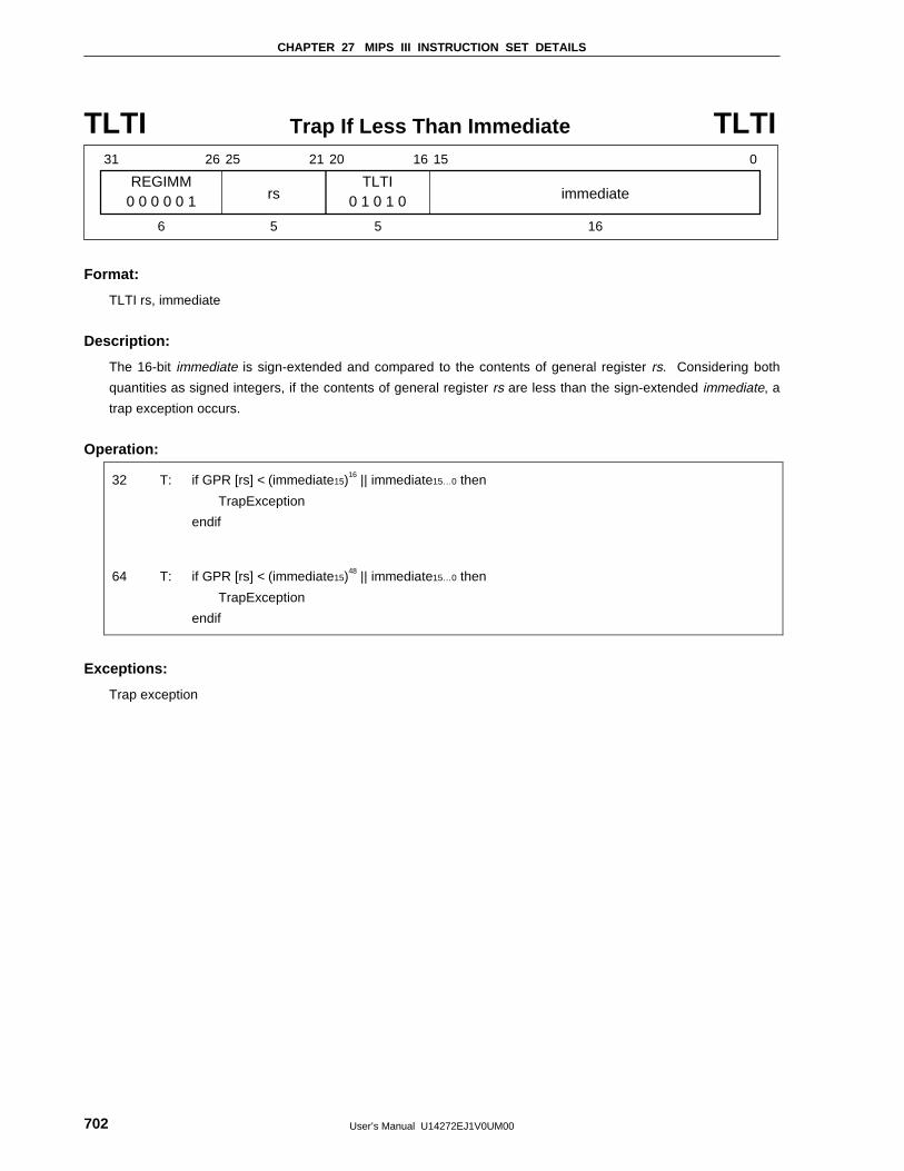
CHAPTER 27 MIPS III INSTRUCTION SET DETAILS
User’s Manual U14272EJ1V0UM00702
TLTI Trap If Less Than Immediate TLTI
REGIMM
31 26 25 21 20 16 15 0
rs0 0 0 0 0 1 immediate
6 5 5 16
TLTI0 1 0 1 0
Format:
TLTI rs, immediate
Description:
The 16-bit immediate is sign-extended and compared to the contents of general register rs. Considering both
quantities as signed integers, if the contents of general register rs are less than the sign-extended immediate, a
trap exception occurs.
Operation:
32 T: if GPR [rs] < (immediate15)16 || immediate15…0 then
TrapException
endif
64 T: if GPR [rs] < (immediate15)48 || immediate15…0 then
TrapException
endif
Exceptions:
Trap exception
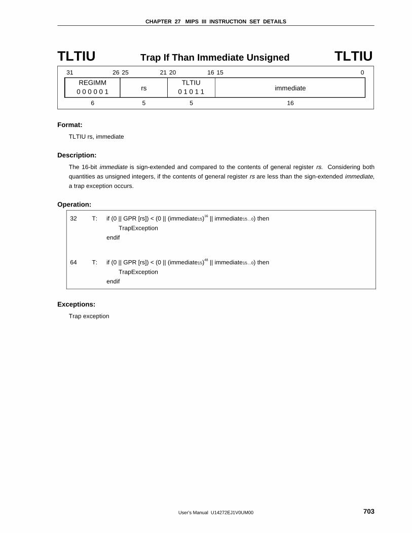
CHAPTER 27 MIPS III INSTRUCTION SET DETAILS
User’s Manual U14272EJ1V0UM00 703
TLTIU Trap If Than Immediate Unsigned TLTIU
REGIMM
31 26 25 21 20 16 15 0
rs0 0 0 0 0 1 immediate
6 5 5 16
TLTIU0 1 0 1 1
Format:
TLTIU rs, immediate
Description:
The 16-bit immediate is sign-extended and compared to the contents of general register rs. Considering both
quantities as unsigned integers, if the contents of general register rs are less than the sign-extended immediate,
a trap exception occurs.
Operation:
32 T: if (0 || GPR [rs]) < (0 || (immediate15)16 || immediate15…0) then
TrapException
endif
64 T: if (0 || GPR [rs]) < (0 || (immediate15)48 || immediate15…0) then
TrapException
endif
Exceptions:
Trap exception

CHAPTER 27 MIPS III INSTRUCTION SET DETAILS
User’s Manual U14272EJ1V0UM00704
TLTU Trap If Less Than Unsigned TLTU
SPECIAL
31 26 25 21 20 16 15 6 5 0
rs0 0 0 0 0 0 rtTLTU
1 1 0 0 1 1
6 5 5 10 6
code
Format:
TLTU rs, rt
Description:
The contents of general register rt are compared to general register rs. Considering both quantities as unsigned
integers, if the contents of general register rs are less than the contents of general register rt, a trap exception
occurs.
The code field is available for use as software parameters, but is retrieved by the exception handler only by
loading the contents of the memory word containing the instruction.
Operation:
32, 64 T: if (0 || GPR [rs]) < (0 || GPR [rt]) then
TrapException
endif
Exceptions:
Trap exception

CHAPTER 27 MIPS III INSTRUCTION SET DETAILS
User’s Manual U14272EJ1V0UM00 705
TNE Trap If Not Equal TNE
SPECIAL
31 26 25 21 20 16 15 6 5 0
rs0 0 0 0 0 0 rtTNE
1 1 0 1 1 0
6 5 5 10 6
code
Format:
TNE rs, rt
Description:
The contents of general register rt are compared to general register rs. If the contents of general register rs are
not equal to the contents of general register rt, a trap exception occurs.
The code field is available for use as software parameters, but is retrieved by the exception handler only by
loading the contents of the memory word containing the instruction.
Operation:
32, 64 T: if GPR [rs] ≠ GPR [rt] then
TrapException
endif
Exceptions:
Trap exception

CHAPTER 27 MIPS III INSTRUCTION SET DETAILS
User’s Manual U14272EJ1V0UM00706
TNEI Trap If Not Equal Immediate TNEI
REGIMM
31 26 25 21 20 16 15 0
rs0 0 0 0 0 1 immediate
6 5 5 16
TNEI0 1 1 1 0
Format:
TNEI rs, immediate
Description:
The 16-bit immediate is sign-extended and compared to the contents of general register rs. If the contents of
general register rs are not equal to the sign-extended immediate, a trap exception occurs.
Operation:
32 T: if GPR [rs] ≠ (immediate15)16 || immediate15…0 then
TrapException
endif
64 T: if GPR [rs] ≠ (immediate15)48 || immediate15…0 then
TrapException
endif
Exceptions:
Trap exception
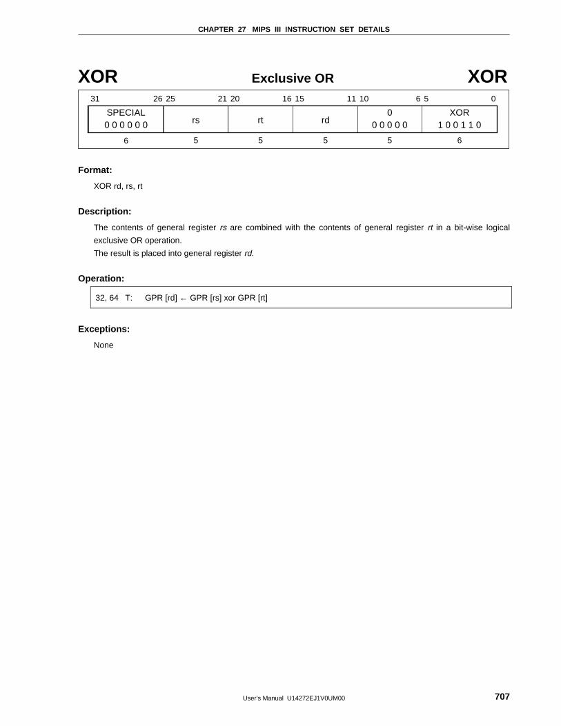
CHAPTER 27 MIPS III INSTRUCTION SET DETAILS
User’s Manual U14272EJ1V0UM00 707
XOR Exclusive OR XOR
SPECIAL
31 26 25 21 20 16 15 11 10 6 5 0
rs0 0 0 0 0 0 rt rd0
0 0 0 0 0XOR
1 0 0 1 1 0
6 5 5 5 5 6
Format:
XOR rd, rs, rt
Description:
The contents of general register rs are combined with the contents of general register rt in a bit-wise logical
exclusive OR operation.
The result is placed into general register rd.
Operation:
32, 64 T: GPR [rd] ← GPR [rs] xor GPR [rt]
Exceptions:
None
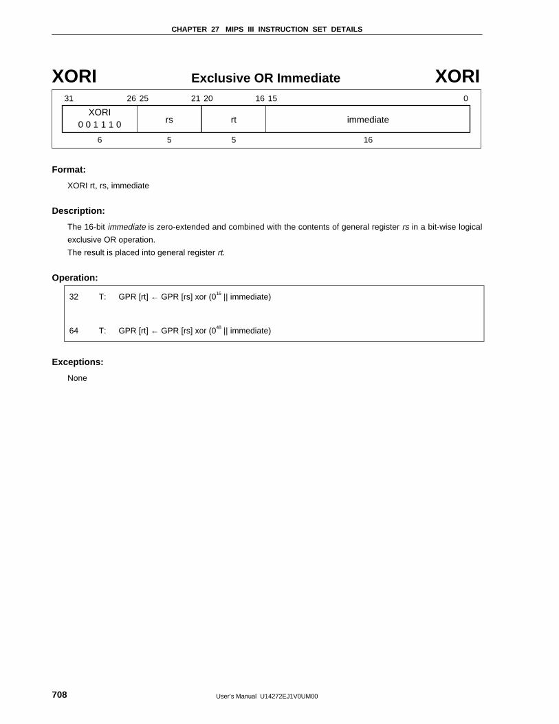
CHAPTER 27 MIPS III INSTRUCTION SET DETAILS
User’s Manual U14272EJ1V0UM00708
XORI Exclusive OR Immediate XORI
XORI
31 26 25 21 20 16 15 0
rs0 0 1 1 1 0 immediate
6 5 5 16
rt
Format:
XORI rt, rs, immediate
Description:
The 16-bit immediate is zero-extended and combined with the contents of general register rs in a bit-wise logical
exclusive OR operation.
The result is placed into general register rt.
Operation:
32 T: GPR [rt] ← GPR [rs] xor (016 || immediate)
64 T: GPR [rt] ← GPR [rs] xor (048 || immediate)
Exceptions:
None
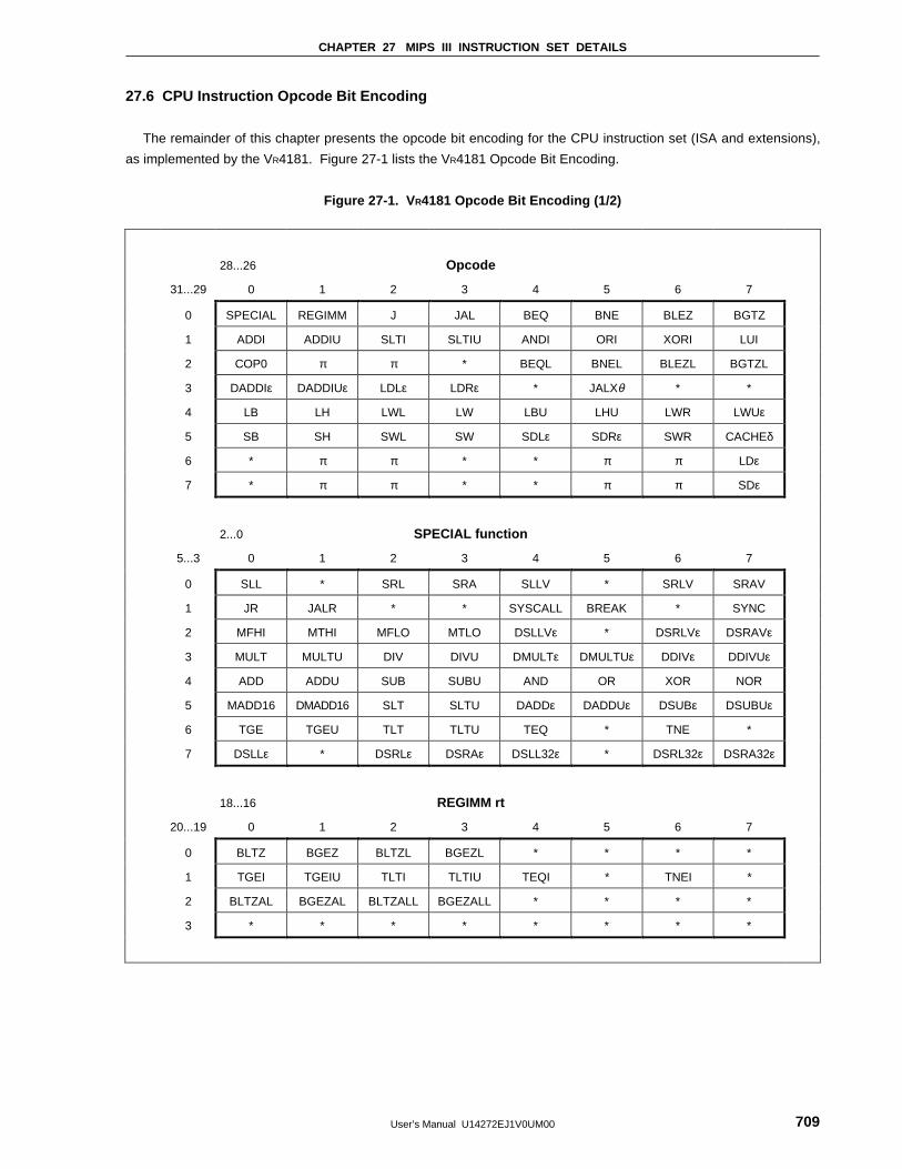
CHAPTER 27 MIPS III INSTRUCTION SET DETAILS
User’s Manual U14272EJ1V0UM00 709
27.6 CPU Instruction Opcode Bit Encoding
The remainder of this chapter presents the opcode bit encoding for the CPU instruction set (ISA and extensions),
as implemented by the VR4181. Figure 27-1 lists the VR4181 Opcode Bit Encoding.
Figure 27-1. V R4181 Opcode Bit Encoding (1/2)
28...26 Opcode
31...29 0 1 2 3 4 5 6 7
0 SPECIAL REGIMM J JAL BEQ BNE BLEZ BGTZ
1 ADDI ADDIU SLTI SLTIU ANDI ORI XORI LUI
2 COP0 π π * BEQL BNEL BLEZL BGTZL
3 DADDIε DADDIUε LDLε LDRε * JALXθ * *
4 LB LH LWL LW LBU LHU LWR LWUε
5 SB SH SWL SW SDLε SDRε SWR CACHEδ
6 * π π * * π π LDε
7 * π π * * π π SDε
2...0 SPECIAL function
5...3 0 1 2 3 4 5 6 7
0 SLL * SRL SRA SLLV * SRLV SRAV
1 JR JALR * * SYSCALL BREAK * SYNC
2 MFHI MTHI MFLO MTLO DSLLVε * DSRLVε DSRAVε
3 MULT MULTU DIV DIVU DMULTε DMULTUε DDIVε DDIVUε
4 ADD ADDU SUB SUBU AND OR XOR NOR
5 MADD16 DMADD16 SLT SLTU DADDε DADDUε DSUBε DSUBUε
6 TGE TGEU TLT TLTU TEQ * TNE *
7 DSLLε * DSRLε DSRAε DSLL32ε * DSRL32ε DSRA32ε
18...16 REGIMM rt
20...19 0 1 2 3 4 5 6 7
0 BLTZ BGEZ BLTZL BGEZL * * * *
1 TGEI TGEIU TLTI TLTIU TEQI * TNEI *
2 BLTZAL BGEZAL BLTZALL BGEZALL * * * *
3 * * * * * * * *
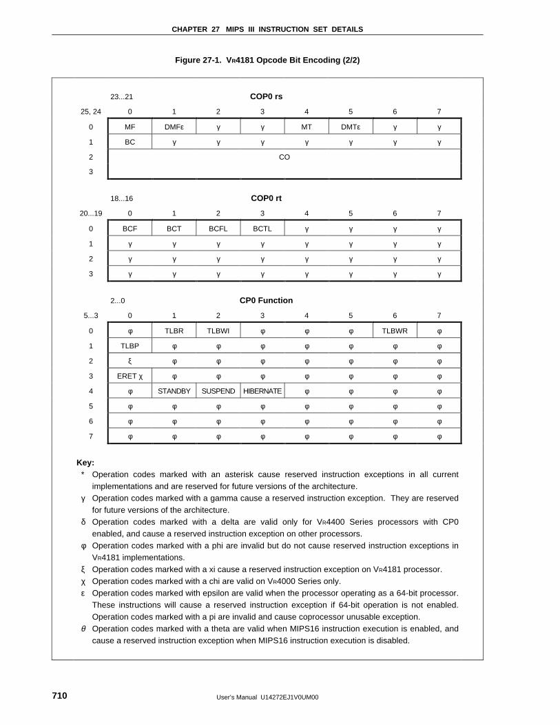
CHAPTER 27 MIPS III INSTRUCTION SET DETAILS
User’s Manual U14272EJ1V0UM00710
Figure 27-1. V R4181 Opcode Bit Encoding (2/2)
23...21 COP0 rs
25, 24 0 1 2 3 4 5 6 7
0 MF DMFε γ γ MT DMTε γ γ
1 BC γ γ γ γ γ γ γ
2 CO
3
18...16 COP0 rt
20...19 0 1 2 3 4 5 6 7
0 BCF BCT BCFL BCTL γ γ γ γ
1 γ γ γ γ γ γ γ γ
2 γ γ γ γ γ γ γ γ
3 γ γ γ γ γ γ γ γ
2...0 CP0 Function
5...3 0 1 2 3 4 5 6 7
0 φ TLBR TLBWI φ φ φ TLBWR φ
1 TLBP φ φ φ φ φ φ φ
2 ξ φ φ φ φ φ φ φ
3 ERET χ φ φ φ φ φ φ φ
4 φ STANDBY SUSPEND HIBERNATE φ φ φ φ
5 φ φ φ φ φ φ φ φ
6 φ φ φ φ φ φ φ φ
7 φ φ φ φ φ φ φ φ
Key: * Operation codes marked with an asterisk cause reserved instruction exceptions in all current
implementations and are reserved for future versions of the architecture. γ Operation codes marked with a gamma cause a reserved instruction exception. They are reserved
for future versions of the architecture. δ Operation codes marked with a delta are valid only for VR4400 Series processors with CP0
enabled, and cause a reserved instruction exception on other processors. φ Operation codes marked with a phi are invalid but do not cause reserved instruction exceptions in
VR4181 implementations. ξ Operation codes marked with a xi cause a reserved instruction exception on VR4181 processor. χ Operation codes marked with a chi are valid on VR4000 Series only. ε Operation codes marked with epsilon are valid when the processor operating as a 64-bit processor.
These instructions will cause a reserved instruction exception if 64-bit operation is not enabled.Operation codes marked with a pi are invalid and cause coprocessor unusable exception.
θ Operation codes marked with a theta are valid when MIPS16 instruction execution is enabled, andcause a reserved instruction exception when MIPS16 instruction execution is disabled.
User’s Manual U14272EJ1V0UM00 711
CHAPTER 28 MIPS16 INSTRUCTION SET FORMAT
This chapter describes the format of each MIPS16 instruction, and the format of the MIPS instructions that are
made by converting MIPS16 instructions in alphabetical order. For details of MIPS16 instruction conversion and
opcode, refer to CHAPTER 4 MIPS16 INSTRUCTION SET.
Caution For some instructions, their format or syntax may become ineffective after they are converted to
a 32-bit instruction. For details of formats and syntax of 32-bit instructions, refer to CHAPTER 3
MIPS III INSTRUCTION SET SUMMARY and CHAPTER 27 MIPS III INSTRUCTION SET DETAILS.
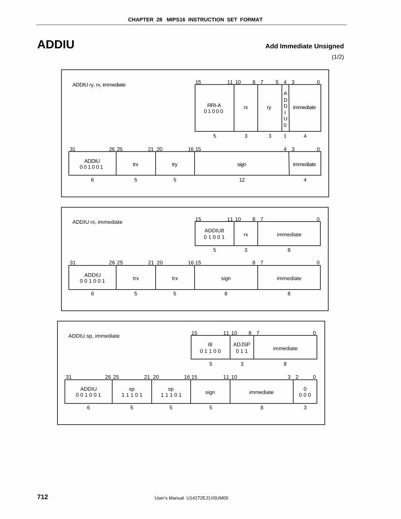
CHAPTER 28 MIPS16 INSTRUCTION SET FORMAT
User’s Manual U14272EJ1V0UM00712
ADDIU Add Immediate Unsigned
(1/2)
0341516 2021252631
4
034578101115
4
ADDIU0 0 1 0 0 1 trx try sign immediate
12556
335
immediateryrxRRI-A0 1 0 0 0
ADDIU ry, rx, immediate
ADDIU0
1
0781516 2021252631
8
078101115
8
ADDIU0 0 1 0 0 1 trx trx sign immediate
8556
35
immediaterxADDIU80 1 0 0 1
ADDIU rx, immediate
02310111516 2021252631
8
078101115
8
ADDIU0 0 1 0 0 1
sp1 1 1 0 1
sp1 1 1 0 1 sign immediate
5556
35
immediateADJSP0 1 1
I80 1 1 0 0
ADDIU sp, immediate
00 0 0
3
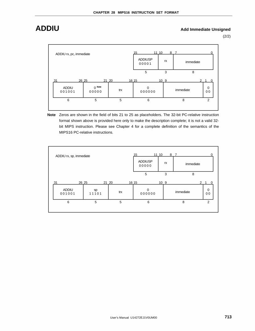
CHAPTER 28 MIPS16 INSTRUCTION SET FORMAT
User’s Manual U14272EJ1V0UM00 713
ADDIU Add Immediate Unsigned
(2/2)
1 021516 2021252631
8
078101115
8
ADDIU0 0 1 0 0 1
00 0 0 0 0 trx
00 0 0 0 0 0 immediate
6556
35
immediaterxADDIUSP0 0 0 0 1
ADDIU rx, pc, immediate
00 0
2
910
Note
Note Zeros are shown in the field of bits 21 to 25 as placeholders. The 32-bit PC-relative instruction
format shown above is provided here only to make the description complete; it is not a valid 32-
bit MIPS instruction. Please see Chapter 4 for a complete definition of the semantics of the
MIPS16 PC-relative instructions.
1 021516 2021252631
8
078101115
8
ADDIU0 0 1 0 0 1
sp1 1 1 0 1 trx
00 0 0 0 0 0 immediate
6556
35
immediaterxADDIUSP0 0 0 0 0
ADDIU rx, sp, immediate
00 0
2
910
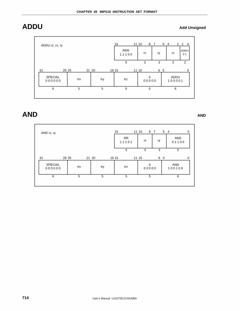
CHAPTER 28 MIPS16 INSTRUCTION SET FORMAT
User’s Manual U14272EJ1V0UM00714
ADDU Add Unsigned
05610111516 2021252631
6
1 024578101115
3
SPECIAL0 0 0 0 0 0 trx try
00 0 0 0 0
ADDU1 0 0 0 0 1
5556
335
ADDU0 1ryrx
RRR1 1 1 0 0
ADDU rz, rx, ry
rz
2
trz
5
AND AND
05610111516 20212631
6
04578101115
5
SPECIAL0 0 0 0 0 0 trx try trx
AND1 0 0 1 0 0
5556
335
AND0 1 1 0 0ryrx
RR1 1 1 0 1
AND rx, ry
00 0 0 0 0
5
25
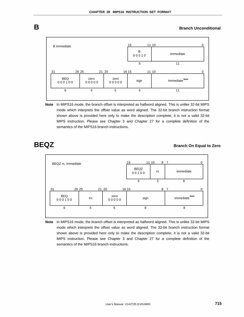
CHAPTER 28 MIPS16 INSTRUCTION SET FORMAT
User’s Manual U14272EJ1V0UM00 715
B Branch Unconditional
0101115 2021252631
11
0101115
11
BEQ0 0 0 1 0 0
zero0 0 0 0 0 immediateNote
5556
5
immediateB
0 0 0 1 0
B immediate
zero0 0 0 0 0 sign
16
Note In MIPS16 mode, the branch offset is interpreted as halfword aligned. This is unlike 32-bit MIPS
mode which interprets the offset value as word aligned. The 32-bit branch instruction format
shown above is provided here only to make the description complete; it is not a valid 32-bit
MIPS instruction. Please see Chapter 3 and Chapter 27 for a complete definition of the
semantics of the MIPS16 branch instructions.
BEQZ Branch On Equal to Zero
0781516 2021252631
8
078101115
8
BEQ0 0 0 1 0 0 trx
zero0 0 0 0 0 sign immediate
Note
8556
35
immediaterxBEQZ
0 0 1 0 0
BEQZ rx, immediate
Note In MIPS16 mode, the branch offset is interpreted as halfword aligned. This is unlike 32-bit MIPS
mode which interprets the offset value as word aligned. The 32-bit branch instruction format
shown above is provided here only to make the description complete; it is not a valid 32-bit
MIPS instruction. Please see Chapter 3 and Chapter 27 for a complete definition of the
semantics of the MIPS16 branch instructions.
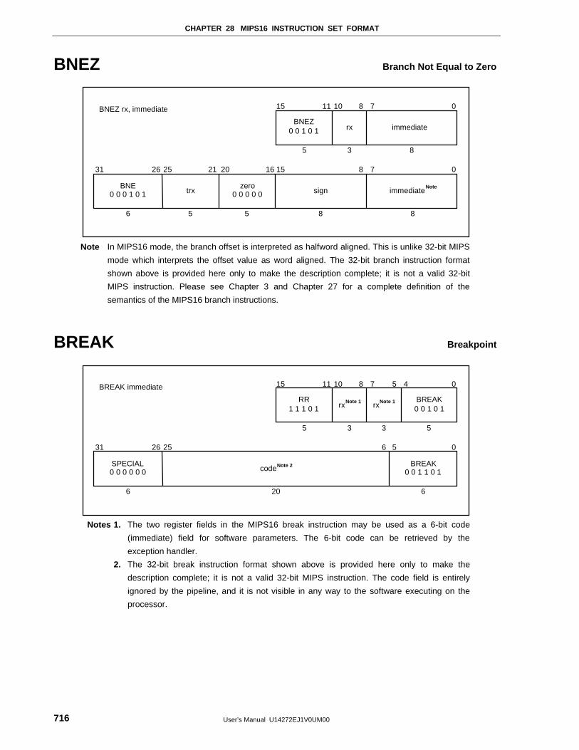
CHAPTER 28 MIPS16 INSTRUCTION SET FORMAT
User’s Manual U14272EJ1V0UM00716
BNEZ Branch Not Equal to Zero
0781516 2021252631
8
078101115
8
BNE0 0 0 1 0 1 trx
zero0 0 0 0 0 sign immediate
Note
8556
35
immediaterxBNEZ
0 0 1 0 1
BNEZ rx, immediate
Note In MIPS16 mode, the branch offset is interpreted as halfword aligned. This is unlike 32-bit MIPS
mode which interprets the offset value as word aligned. The 32-bit branch instruction format
shown above is provided here only to make the description complete; it is not a valid 32-bit
MIPS instruction. Please see Chapter 3 and Chapter 27 for a complete definition of the
semantics of the MIPS16 branch instructions.
BREAK Breakpoint
056252631
6
04578101115
5
SPECIAL0 0 0 0 0 0 codeNote 2 BREAK
0 0 1 1 0 1
206
335
BREAK0 0 1 0 1rx
Note 1rx
Note 1RR1 1 1 0 1
BREAK immediate
Notes 1. The two register fields in the MIPS16 break instruction may be used as a 6-bit code
(immediate) field for software parameters. The 6-bit code can be retrieved by the
exception handler.
2. The 32-bit break instruction format shown above is provided here only to make the
description complete; it is not a valid 32-bit MIPS instruction. The code field is entirely
ignored by the pipeline, and it is not visible in any way to the software executing on the
processor.
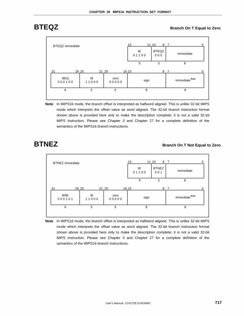
CHAPTER 28 MIPS16 INSTRUCTION SET FORMAT
User’s Manual U14272EJ1V0UM00 717
BTEQZ Branch On T Equal to Zero
0781516 2021252631
8
078101115
8
BEQ0 0 0 1 0 0
t81 1 0 0 0
zero0 0 0 0 0 sign immediateNote
8556
35
immediateBTEQZ0 0 0
I80 1 1 0 0
BTEQZ immediate
Note In MIPS16 mode, the branch offset is interpreted as halfword aligned. This is unlike 32-bit MIPS
mode which interprets the offset value as word aligned. The 32-bit branch instruction format
shown above is provided here only to make the description complete; it is not a valid 32-bit
MIPS instruction. Please see Chapter 3 and Chapter 27 for a complete definition of the
semantics of the MIPS16 branch instructions.
BTNEZ Branch On T Not Equal to Zero
0781516 2021252631
8
078101115
8
BNE0 0 0 1 0 1
t81 1 0 0 0
zero0 0 0 0 0 sign immediateNote
8556
35
immediateBTNEZ0 0 1
I80 1 1 0 0
BTNEZ immediate
Note In MIPS16 mode, the branch offset is interpreted as halfword aligned. This is unlike 32-bit MIPS
mode which interprets the offset value as word aligned. The 32-bit branch instruction format
shown above is provided here only to make the description complete; it is not a valid 32-bit
MIPS instruction. Please see Chapter 3 and Chapter 27 for a complete definition of the
semantics of the MIPS16 branch instructions.
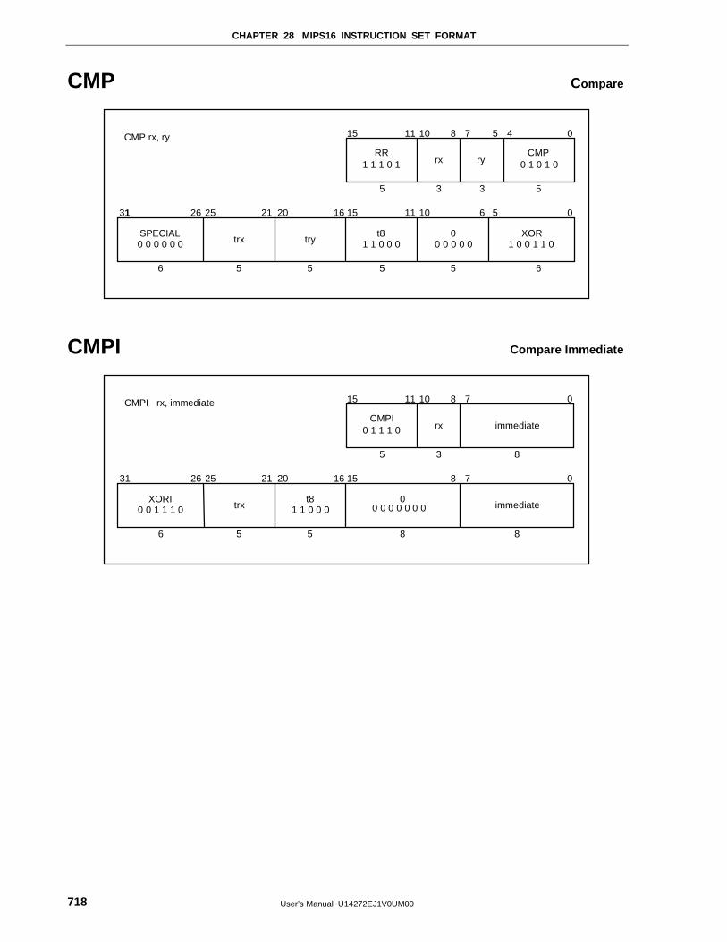
CHAPTER 28 MIPS16 INSTRUCTION SET FORMAT
User’s Manual U14272EJ1V0UM00718
CMP Compare
05610111516 20212631
6
04578101115
5
SPECIAL0 0 0 0 0 0 trx try
t81 1 0 0 0
XOR1 0 0 1 1 0
5556
335
CMP0 1 0 1 0ryrx
RR1 1 1 0 1
CMP rx, ry
00 0 0 0 0
5
25
CMPI Compare Immediate
0781516 2021252631
8
078101115
8
XORI0 0 1 1 1 0 trx
t81 1 0 0 0
00 0 0 0 0 0 00
immediate
8556
35
immediaterxCMPI
0 1 1 1 0
CMPI rx, immediate
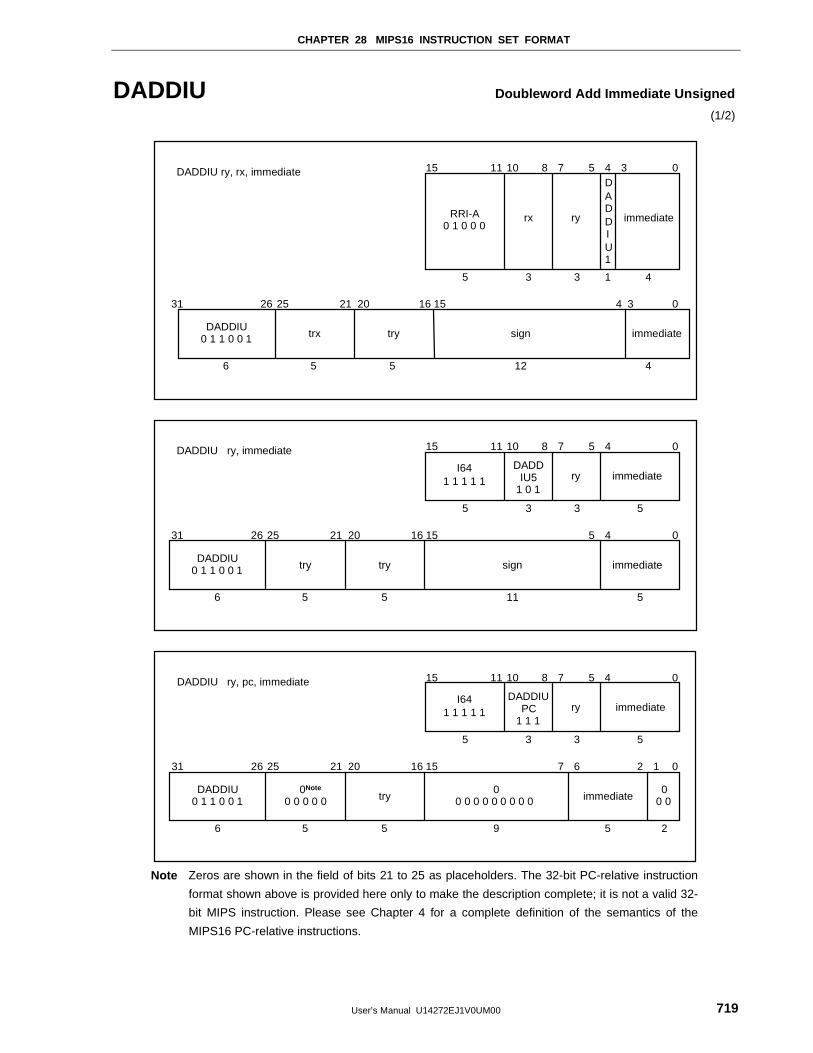
CHAPTER 28 MIPS16 INSTRUCTION SET FORMAT
User’s Manual U14272EJ1V0UM00 719
DADDIU Doubleword Add Immediate Unsigned
(1/2)
0341516 2021252631
4
034578101115
4
DADDIU0 1 1 0 0 1 trx try sign immediate
12556
335
immediateryrxRRI-A0 1 0 0 0
DADDIU ry, rx, immediateDADDIU1
1
0451516 2021252631
5
04578101115
5
DADDIU0 1 1 0 0 1 try try sign immediate
11556
335
immediateryDADD
IU51 0 1
I641 1 1 1 1
DADDIU ry, immediate
1 02671516 2021252631
5
04578101115
5
DADDIU0 1 1 0 0 1
00 0 0 0 0 try
00 0 0 0 0 0 0 0 0 immediate
9556
335
immediateryDADDIU
PC1 1 1
I641 1 1 1 1
DADDIU ry, pc, immediate
00 0
2
Note
Note Zeros are shown in the field of bits 21 to 25 as placeholders. The 32-bit PC-relative instruction
format shown above is provided here only to make the description complete; it is not a valid 32-
bit MIPS instruction. Please see Chapter 4 for a complete definition of the semantics of the
MIPS16 PC-relative instructions.
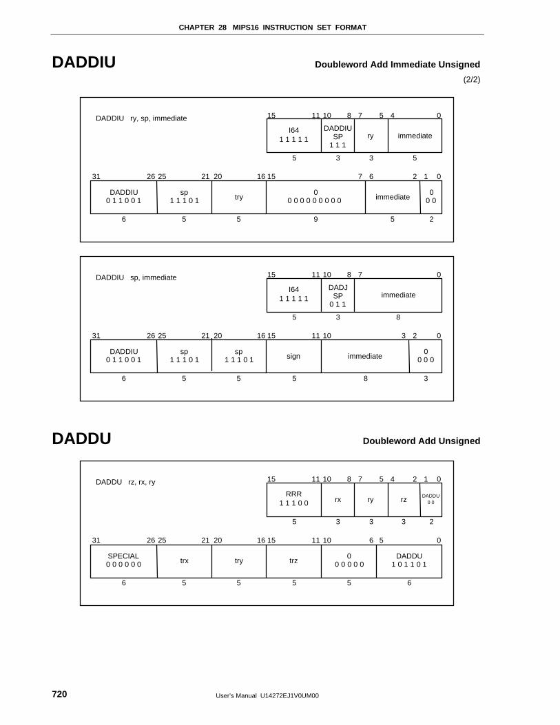
CHAPTER 28 MIPS16 INSTRUCTION SET FORMAT
User’s Manual U14272EJ1V0UM00720
DADDIU Doubleword Add Immediate Unsigned
(2/2)
1 02671516 2021252631
5
04578101115
5
DADDIU0 1 1 0 0 1
sp1 1 1 0 1 try
00 0 0 0 0 0 0 0 0 immediate
9556
335
immediateryDADDIU
SP1 1 1
I641 1 1 1 1
DADDIU ry, sp, immediate
00 0
2
02310111516 2021252631
8
078101115
8
DADDIU0 1 1 0 0 1
sp1 1 1 0 1
sp1 1 1 0 1 sign immediate
5556
35
immediateDADJ
SP0 1 1
I641 1 1 1 1
DADDIU sp, immediate
00 0 0
3
DADDU Doubleword Add Unsigned
05610111516 2021252631
6
1 024578101115
3
SPECIAL0 0 0 0 0 0 trx try
00 0 0 0 0
DADDU1 0 1 1 0 1
5556
335
DADDU0 0ryrx
RRR1 1 1 0 0
DADDU rz, rx, ry
rz
2
trz
5
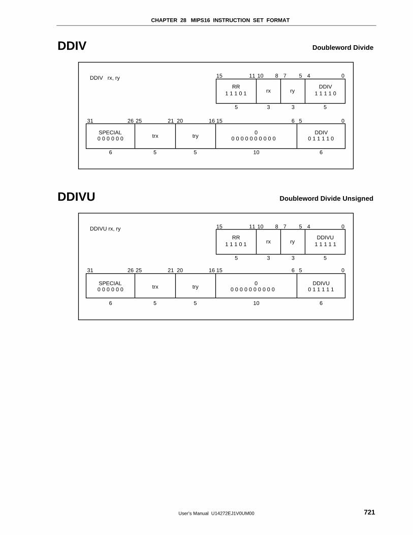
CHAPTER 28 MIPS16 INSTRUCTION SET FORMAT
User’s Manual U14272EJ1V0UM00 721
DDIV Doubleword Divide
0561516 2021252631
6
04578101115
5
SPECIAL0 0 0 0 0 0 trx try
00 0 0 0 0 0 0 0 0 0
DDIV0 1 1 1 1 0
10556
335
DDIV1 1 1 1 0ryrx
RR1 1 1 0 1
DDIV rx, ry
DDIVU Doubleword Divide Unsigned
0561516 2021252631
6
04578101115
5
SPECIAL0 0 0 0 0 0 trx try
00 0 0 0 0 0 0 0 0 0
DDIVU0 1 1 1 1 1
10556
335
DDIVU1 1 1 1 1ryrx
RR1 1 1 0 1
DDIVU rx, ry
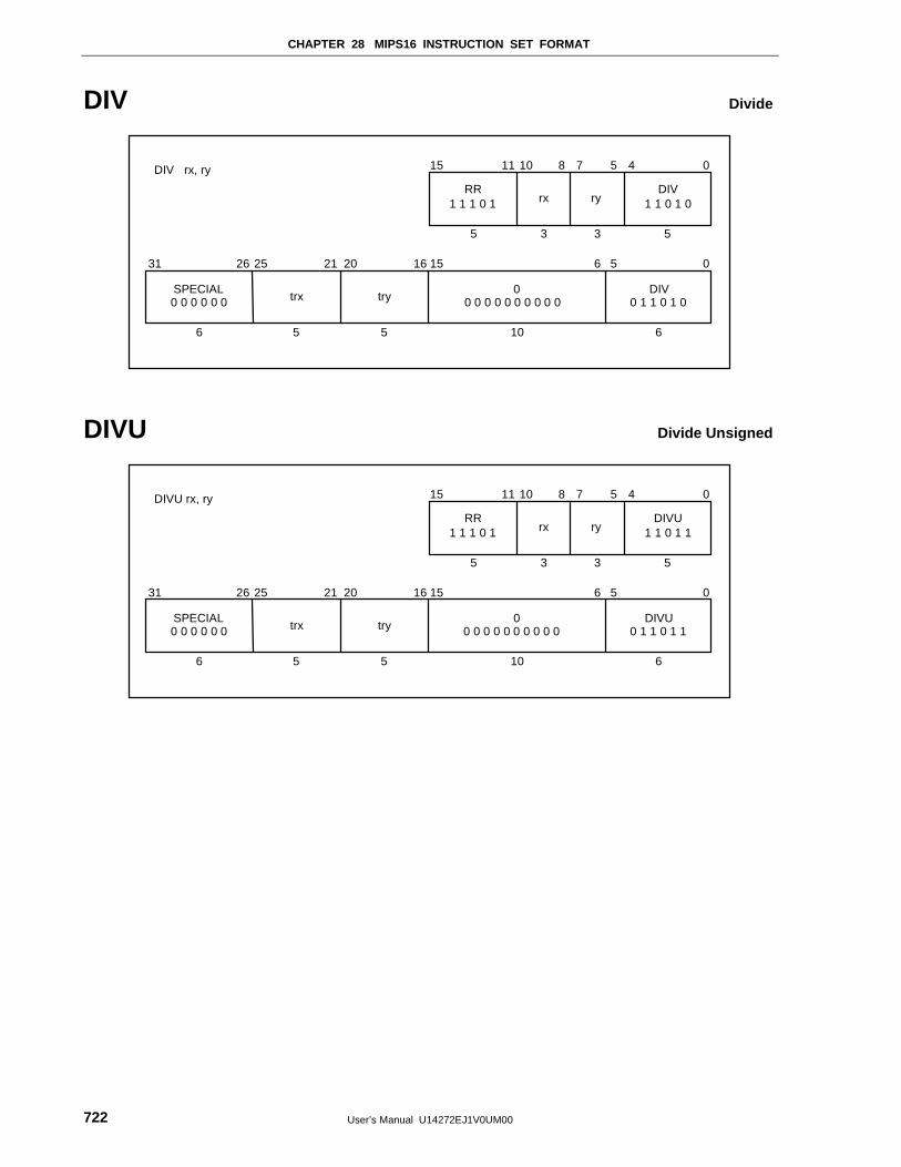
CHAPTER 28 MIPS16 INSTRUCTION SET FORMAT
User’s Manual U14272EJ1V0UM00722
DIV Divide
0561516 2021252631
6
04578101115
5
SPECIAL0 0 0 0 0 0 trx try
00 0 0 0 0 0 0 0 0 0
DIV0 1 1 0 1 0
10556
335
DIV1 1 0 1 0ryrx
RR1 1 1 0 1
DIV rx, ry
DIVU Divide Unsigned
0561516 2021252631
6
04578101115
5
SPECIAL0 0 0 0 0 0 trx try
00 0 0 0 0 0 0 0 0 0
DIVU0 1 1 0 1 1
10556
335
DIVU1 1 0 1 1ryrx
RR1 1 1 0 1
DIVU rx, ry
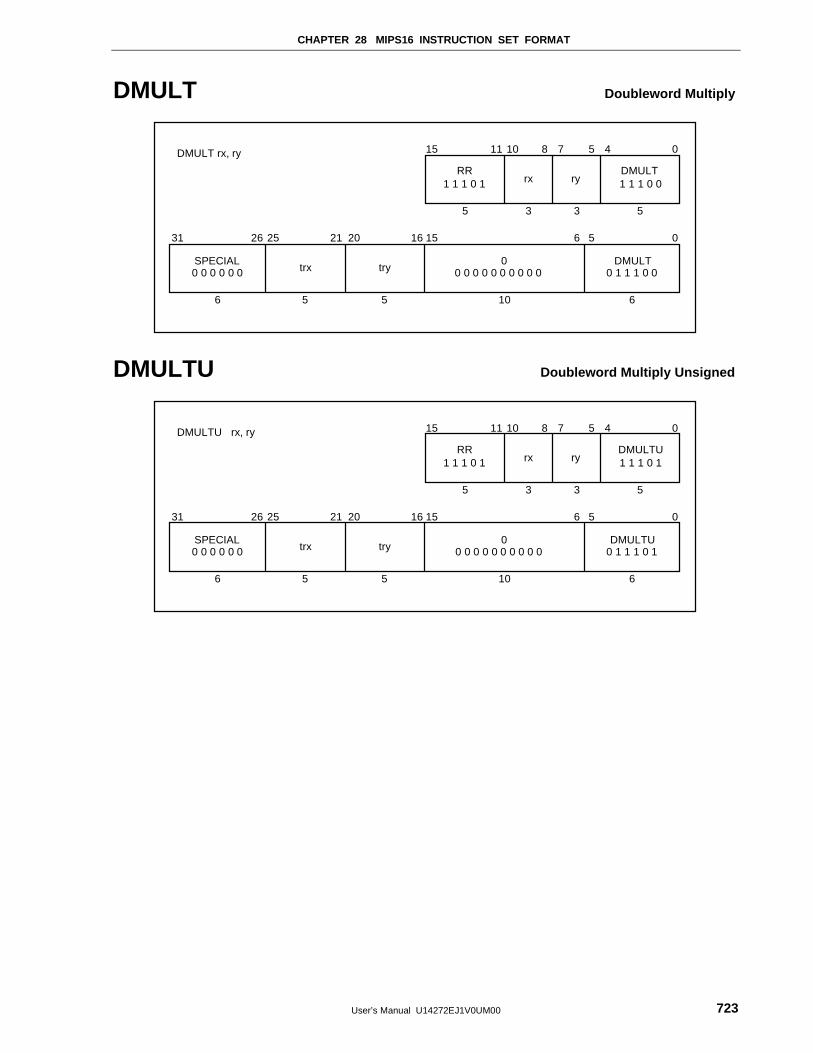
CHAPTER 28 MIPS16 INSTRUCTION SET FORMAT
User’s Manual U14272EJ1V0UM00 723
DMULT Doubleword Multiply
0561516 2021252631
6
04578101115
5
SPECIAL0 0 0 0 0 0 trx try
00 0 0 0 0 0 0 0 0 0
DMULT0 1 1 1 0 0
10556
335
DMULT1 1 1 0 0ryrx
RR1 1 1 0 1
DMULT rx, ry
DMULTU Doubleword Multiply Unsigned
0561516 2021252631
6
04578101115
5
SPECIAL0 0 0 0 0 0 trx try
00 0 0 0 0 0 0 0 0 0
DMULTU0 1 1 1 0 1
10556
335
DMULTU1 1 1 0 1ryrx
RR1 1 1 0 1
DMULTU rx, ry
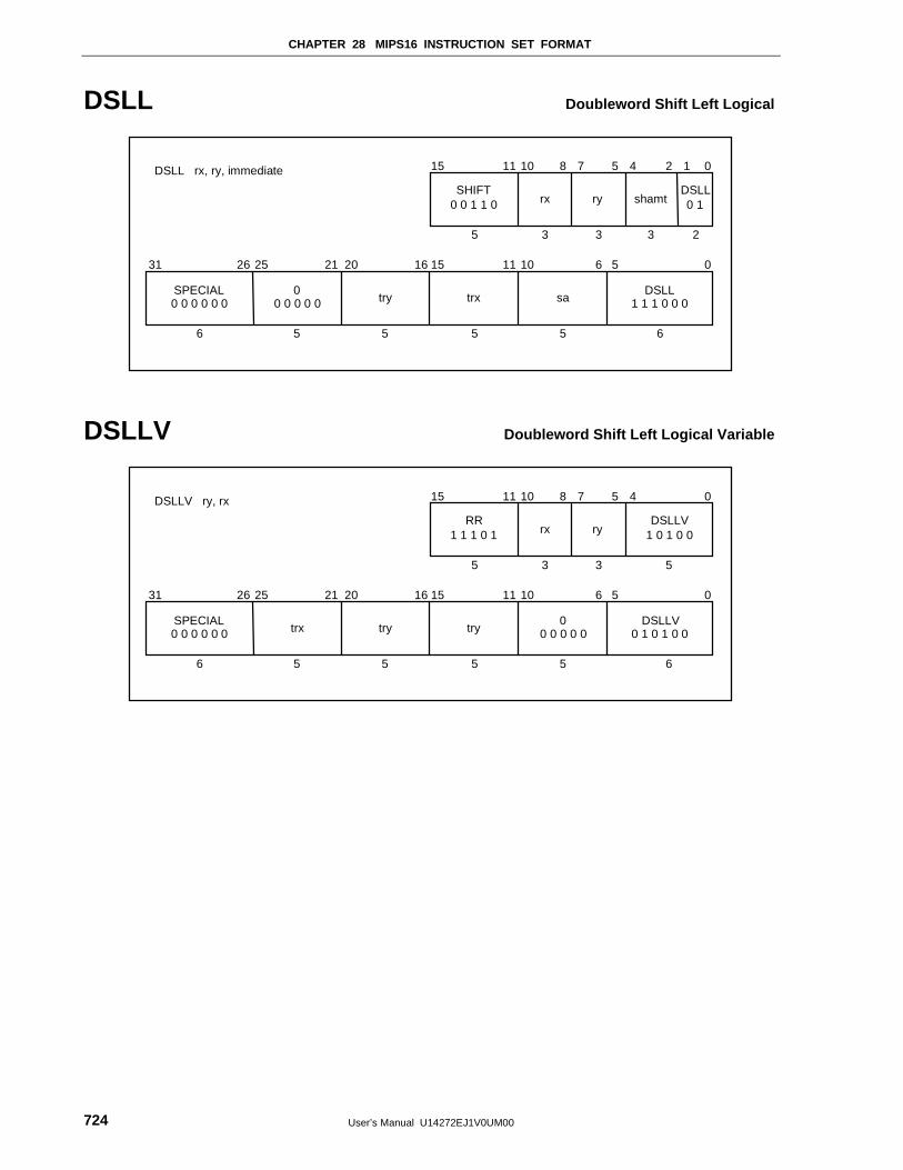
CHAPTER 28 MIPS16 INSTRUCTION SET FORMAT
User’s Manual U14272EJ1V0UM00724
DSLL Doubleword Shift Left Logical
05610111516 2021252631
6
1 024578101115
3
SPECIAL0 0 0 0 0 0
00 0 0 0 0 try sa
DSLL1 1 1 0 0 0
5556
335
DSLL0 1ryrx
SHIFT0 0 1 1 0
DSLL rx, ry, immediate
shamt
2
trx
5
DSLLV Doubleword Shift Left Logical Variable
05610111516 20212631
6
04578101115
5
SPECIAL0 0 0 0 0 0 trx try try
DSLLV0 1 0 1 0 0
5556
335
DSLLV1 0 1 0 0ryrx
RR1 1 1 0 1
DSLLV ry, rx
00 0 0 0 0
5
25
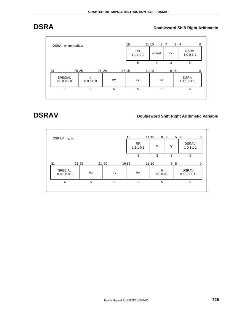
CHAPTER 28 MIPS16 INSTRUCTION SET FORMAT
User’s Manual U14272EJ1V0UM00 725
DSRA Doubleword Shift Right Arithmetic
05610111516 20212631
6
04578101115
5
SPECIAL0 0 0 0 0 0
00 0 0 0 0 try try
DSRA1 1 1 0 1 1
5556
335
DSRA1 0 0 1 1ryshamt
RR1 1 1 0 1
DSRA ry, immediate
sa
5
25
DSRAV Doubleword Shift Right Arithmetic Variable
05610111516 20212631
6
04578101115
5
SPECIAL0 0 0 0 0 0 trx try try
DSRAV0 1 0 1 1 1
5556
335
DSRAV1 0 1 1 1ryrx
RR1 1 1 0 1
DSRAV ry, rx
00 0 0 0 0
5
25
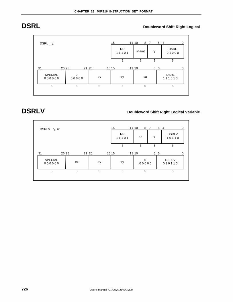
CHAPTER 28 MIPS16 INSTRUCTION SET FORMAT
User’s Manual U14272EJ1V0UM00726
DSRL Doubleword Shift Right Logical
05610111516 20212631
6
04578101115
5
SPECIAL0 0 0 0 0 0
00 0 0 0 0 try try
DSRL1 1 1 0 1 0
5556
335
DSRL0 1 0 0 0ryshamt
RR1 1 1 0 1
DSRL ry,i di
sa
5
25
DSRLV Doubleword Shift Right Logical Variable
05610111516 20212631
6
04578101115
5
SPECIAL0 0 0 0 0 0 trx try try
DSRLV0 1 0 1 1 0
5556
335
DSRLV1 0 1 1 0ryrx
RR1 1 1 0 1
DSRLV ry, rx
00 0 0 0 0
5
25
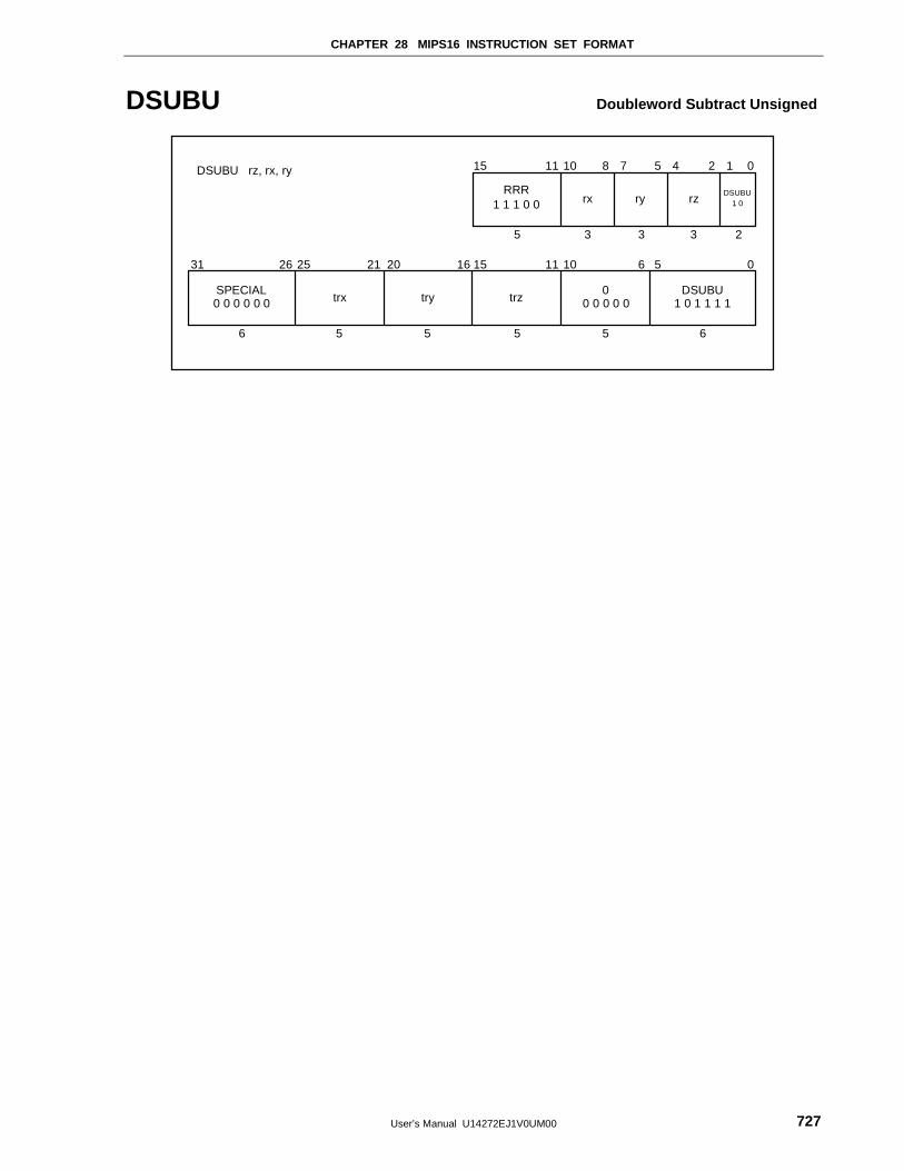
CHAPTER 28 MIPS16 INSTRUCTION SET FORMAT
User’s Manual U14272EJ1V0UM00 727
DSUBU Doubleword Subtract Unsigned
05610111516 2021252631
6
1 024578101115
3
SPECIAL0 0 0 0 0 0 trx try
00 0 0 0 0
DSUBU1 0 1 1 1 1
5556
335
DSUBU1 0ryrx
RRR1 1 1 0 0
DSUBU rz, rx, ry
rz
2
trz
5
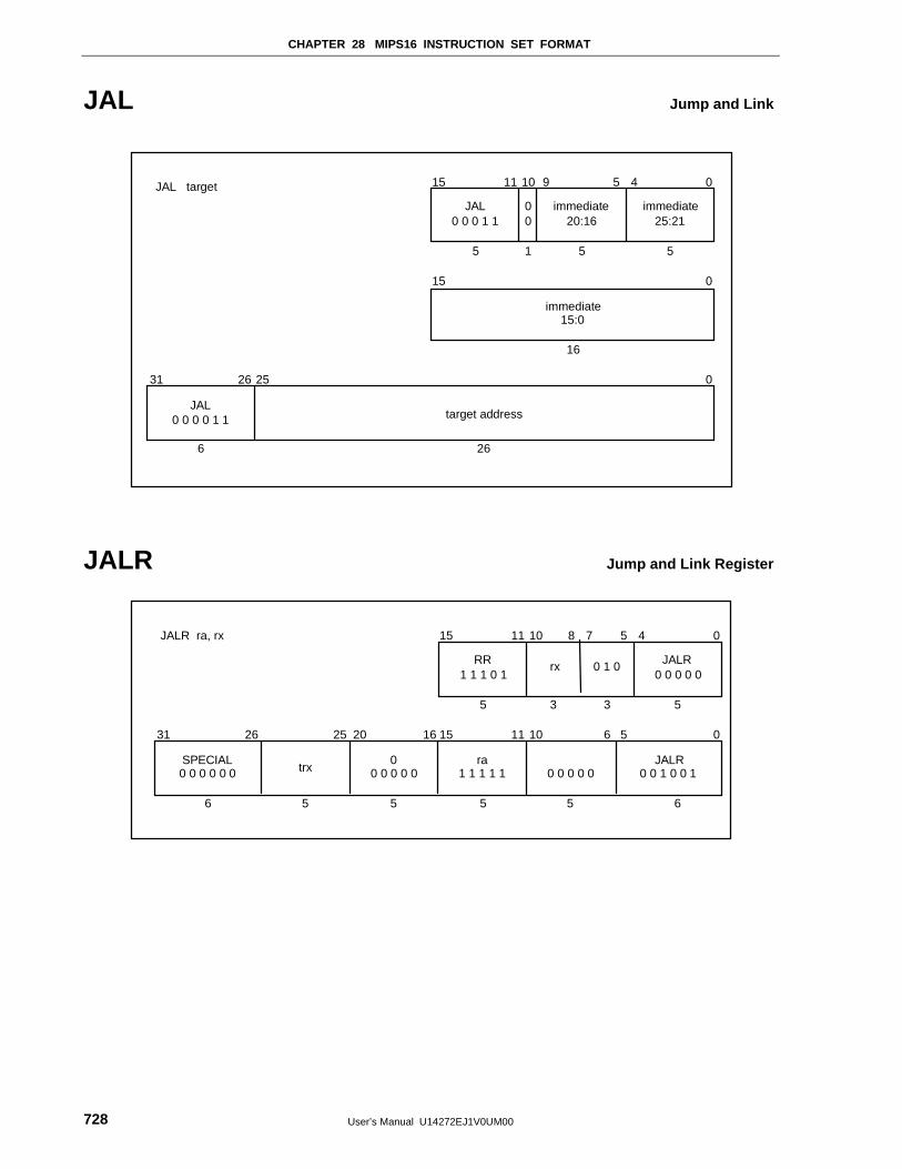
CHAPTER 28 MIPS16 INSTRUCTION SET FORMAT
User’s Manual U14272EJ1V0UM00728
JAL Jump and Link
0252631
015
JAL0 0 0 0 1 1 target address
266
16
immediate15:0
0459101115
5515
immediate25:21
00
JAL0 0 0 1 1
JAL target
immediate20:16
JALR Jump and Link Register
05610111516 20252631
6
04578101115
5
SPECIAL0 0 0 0 0 0 trx
00 0 0 0 0
ra1 1 1 1 1
JALR0 0 1 0 0 1
5556
335
JALR0 0 0 0 0
JALR ra, rx
RR1 1 1 0 1
0 1 0rx
0 0 0 0 0
5
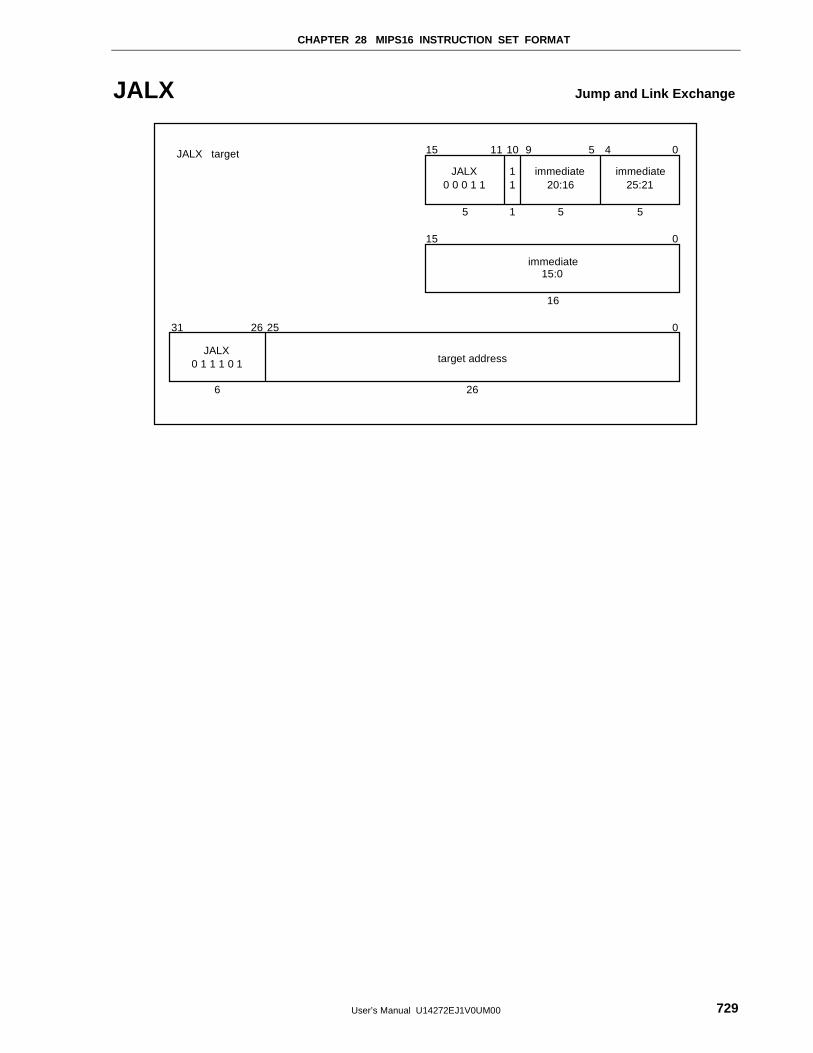
CHAPTER 28 MIPS16 INSTRUCTION SET FORMAT
User’s Manual U14272EJ1V0UM00 729
JALX Jump and Link Exchange
0252631
015
JALX0 1 1 1 0 1 target address
266
16
immediate15:0
0459101115
5515
immediate25:21
11
JALX0 0 0 1 1
JALX target
immediate20:16
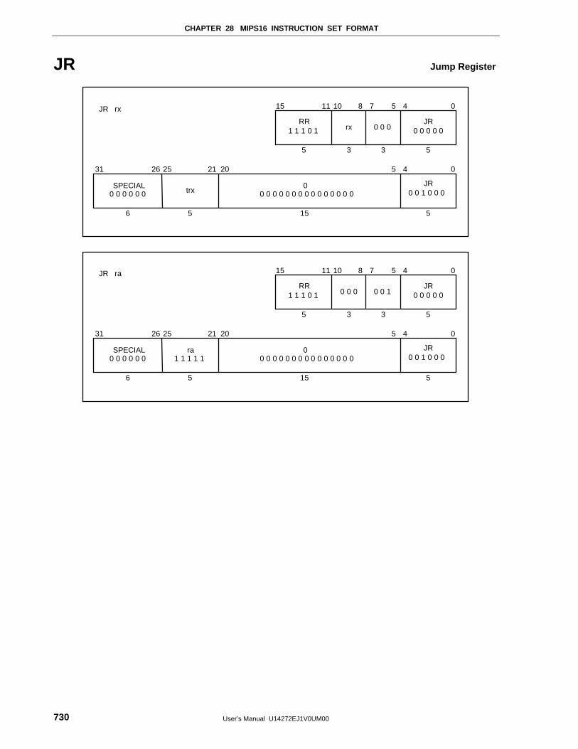
CHAPTER 28 MIPS16 INSTRUCTION SET FORMAT
User’s Manual U14272EJ1V0UM00730
JR Jump Register
045 2021252631
5
04578101115
5
SPECIAL0 0 0 0 0 0 trx
00 0 0 0 0 0 0 0 0 0 0 0 0 0 0
1556
335
0 0 0rxRR
1 1 1 0 1
JR rx
JR0 0 0 0 0
JR0 0 1 0 0 0
045 2021252631
5
04578101115
5
SPECIAL0 0 0 0 0 0
00 0 0 0 0 0 0 0 0 0 0 0 0 0 0
1556
335
0 0 10 0 0RR
1 1 1 0 1
JR ra
JR0 0 0 0 0
JR0 0 1 0 0 0
ra1 1 1 1 1
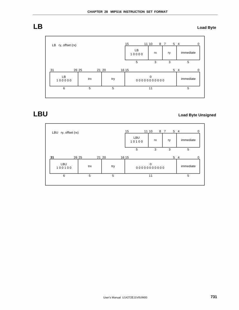
CHAPTER 28 MIPS16 INSTRUCTION SET FORMAT
User’s Manual U14272EJ1V0UM00 731
LB Load Byte
0451516 2021252631
5
04578101115
5
LB1 0 0 0 0 0 trx try
00 0 0 0 0 0 0 0 0 0 0 immediate
11556
335
immediateryrxLB
1 0 0 0 0
LB ry, offset (rx)
LBU Load Byte Unsigned
0451516 2021252631
5
04578101115
5
LBU1 0 0 1 0 0 trx try
00 0 0 0 0 0 0 0 0 0 0 immediate
11556
335
immediateryrxLBU
1 0 1 0 0
LBU ry, offset (rx)
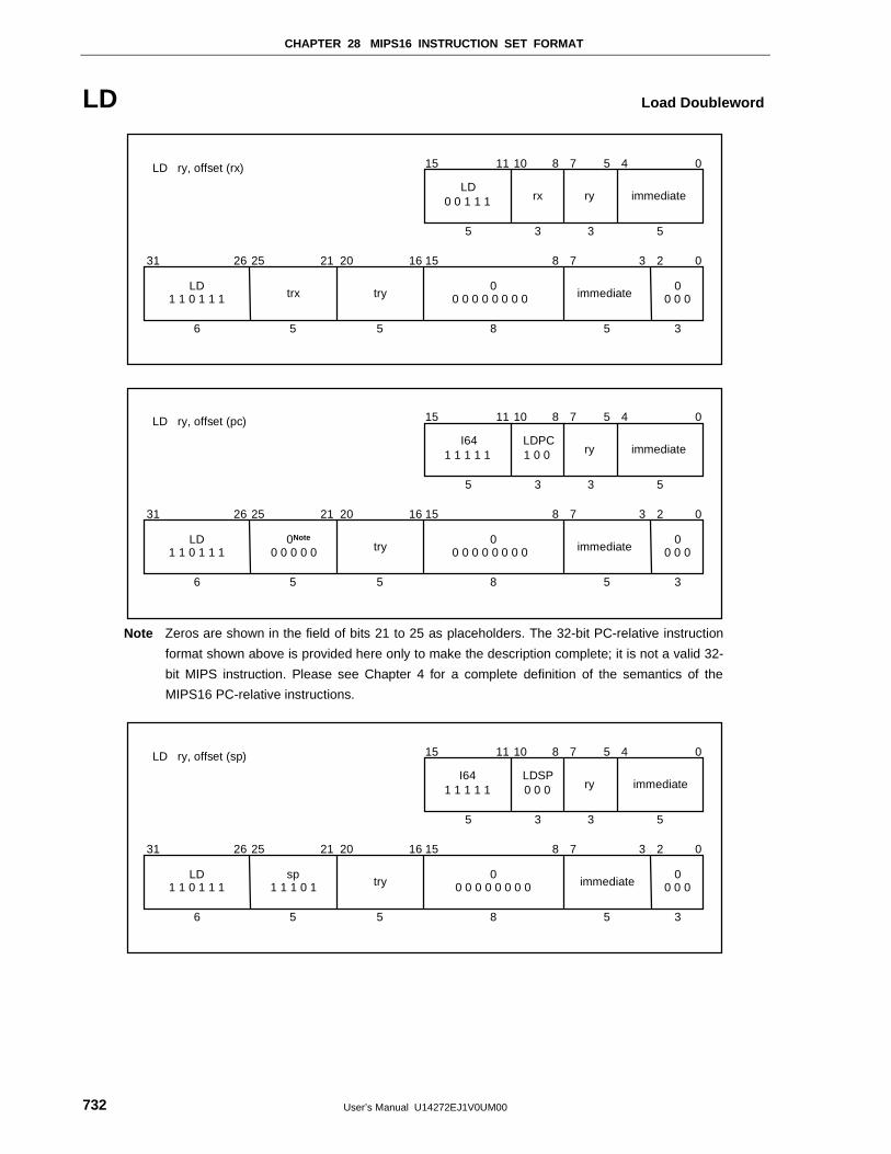
CHAPTER 28 MIPS16 INSTRUCTION SET FORMAT
User’s Manual U14272EJ1V0UM00732
LD Load Doubleword
023781516 2021252631
5
04578101115
5
LD1 1 0 1 1 1 trx try
00 0 0 0 0 0 0 0 immediate
8556
335
immediateryrxLD
0 0 1 1 1
LD ry, offset (rx)
3
00 0 0
023781516 2021252631
5
04578101115
5
LD1 1 0 1 1 1 try
00 0 0 0 0 0 0 0 immediate
8556
335
immediateryI64
1 1 1 1 1
LD ry, offset (pc)
3
00 0 0
LDPC1 0 0
00 0 0 0 0
Note
Note Zeros are shown in the field of bits 21 to 25 as placeholders. The 32-bit PC-relative instruction
format shown above is provided here only to make the description complete; it is not a valid 32-
bit MIPS instruction. Please see Chapter 4 for a complete definition of the semantics of the
MIPS16 PC-relative instructions.
023781516 2021252631
5
04578101115
5
LD1 1 0 1 1 1
sp1 1 1 0 1 try
00 0 0 0 0 0 0 0 immediate
8556
335
immediateryLDSP0 0 0
I641 1 1 1 1
LD ry, offset (sp)
3
00 0 0
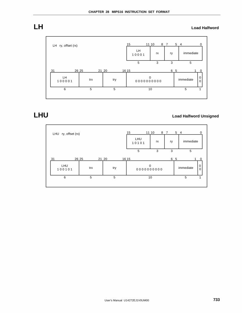
CHAPTER 28 MIPS16 INSTRUCTION SET FORMAT
User’s Manual U14272EJ1V0UM00 733
LH Load Halfword
1 0561516 2021252631
5
04578101115
5
LH1 0 0 0 0 1 trx try
00 0 0 0 0 0 0 0 0 0 immediate
10556
335
immediateryrxLH
1 0 0 0 1
LH ry, offset (rx)
1
00
LHU Load Halfword Unsigned
1 0561516 2021252631
5
04578101115
5
LHU1 0 0 1 0 1 trx try
00 0 0 0 0 0 0 0 0 0 immediate
10556
335
immediateryrxLHU
1 0 1 0 1
LHU ry, offset (rx)
1
00
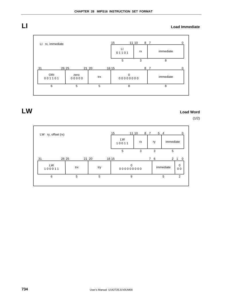
CHAPTER 28 MIPS16 INSTRUCTION SET FORMAT
User’s Manual U14272EJ1V0UM00734
LI Load Immediate
0781516 2021252631
8
078101115
8
ORI0 0 1 1 0 1
zero0 0 0 0 0 trx
00 0 0 0 0 0 0 0 immediate
8556
35
immediaterxLI
0 1 1 0 1
LI rx, immediate
LW Load Word
(1/2)
1 02671516 2021252631
5
04578101115
5
LW1 0 0 0 1 1 trx try
00 0 0 0 0 0 0 0 0 immediate
9556
335
immediateryrxLW
1 0 0 1 1
LW ry, offset (rx)
00 0
2
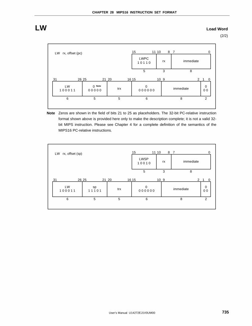
CHAPTER 28 MIPS16 INSTRUCTION SET FORMAT
User’s Manual U14272EJ1V0UM00 735
LW Load Word
(2/2)
1 021516 2021252631
8
078101115
8
LW1 0 0 0 1 1
00 0 0 0 0 trx
00 0 0 0 0 0 immediate
6556
35
immediaterxLWPC
1 0 1 1 0
LW rx, offset (pc)
00 0
2
910
Note
Note Zeros are shown in the field of bits 21 to 25 as placeholders. The 32-bit PC-relative instruction
format shown above is provided here only to make the description complete; it is not a valid 32-
bit MIPS instruction. Please see Chapter 4 for a complete definition of the semantics of the
MIPS16 PC-relative instructions.
1 021516 2021252631
8
078101115
8
LW1 0 0 0 1 1
sp1 1 1 0 1 trx
00 0 0 0 0 0 immediate
6556
35
immediaterxLWSP
1 0 0 1 0
LW rx, offset (sp)
00 0
2
910
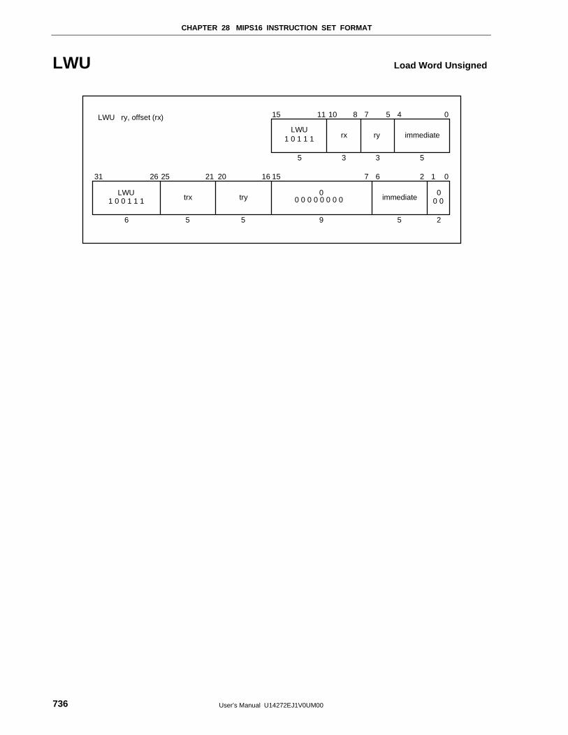
CHAPTER 28 MIPS16 INSTRUCTION SET FORMAT
User’s Manual U14272EJ1V0UM00736
LWU Load Word Unsigned
1 02671516 2021252631
5
04578101115
5
LWU1 0 0 1 1 1 trx try
00 0 0 0 0 0 0 0 immediate
9556
335
immediateryrxLWU
1 0 1 1 1
LWU ry, offset (rx)
00 0
2

CHAPTER 28 MIPS16 INSTRUCTION SET FORMAT
User’s Manual U14272EJ1V0UM00 737
MFHI Move From HI Register
056101115162631
6
04578101115
5
SPECIAL0 0 0 0 0 0
00 0 0 0 0 0 0 0 0 0 trx
MFHI0 1 0 0 0 0
5106
335
rx 0 0 0RR
1 1 1 0 1
MFHI rx
00 0 0 0 0
5
25
MFHI1 0 0 0 0
MFLO Move From LO Register
056101115162631
6
04578101115
5
SPECIAL0 0 0 0 0 0
00 0 0 0 0 0 0 0 0 0 trx
MFLO0 1 0 0 1 0
5106
335
rx 0 0 0RR
1 1 1 0 1
MFLO rx
00 0 0 0 0
5
25
MFLO1 0 0 0 0
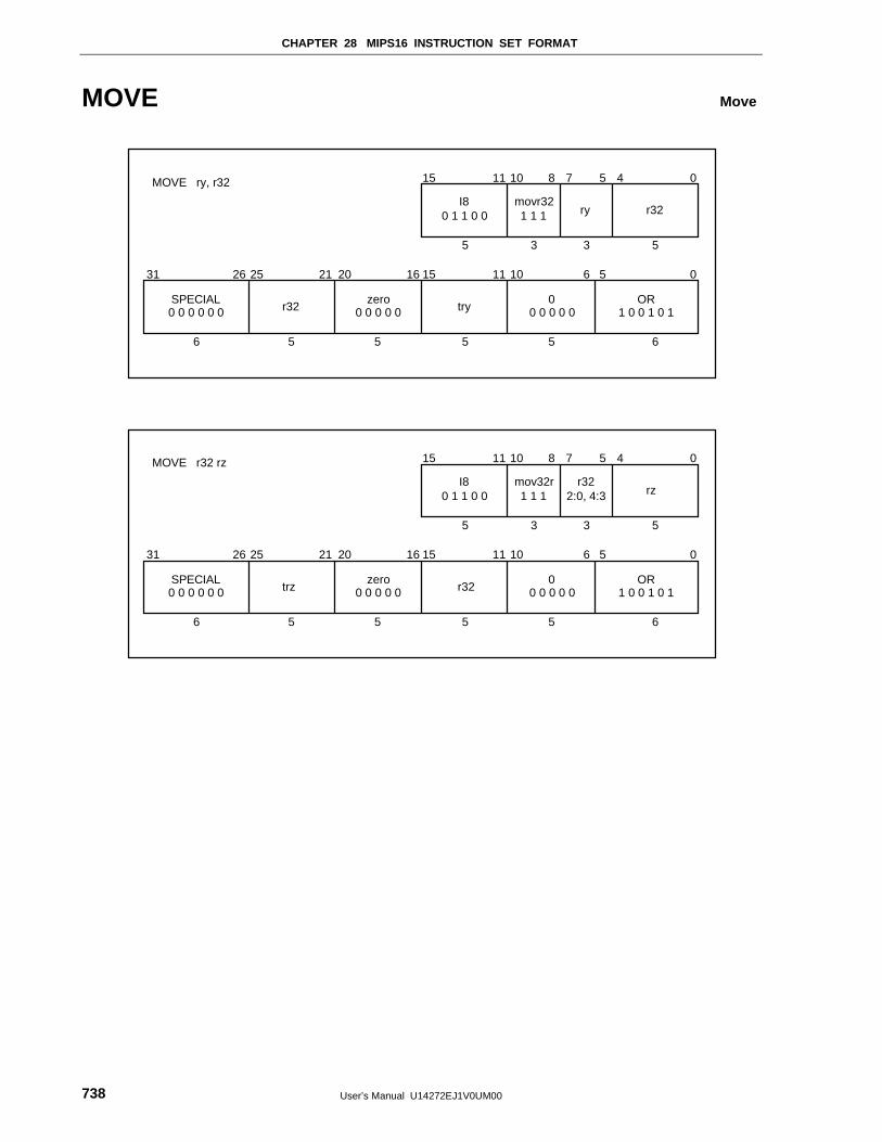
CHAPTER 28 MIPS16 INSTRUCTION SET FORMAT
User’s Manual U14272EJ1V0UM00738
MOVE Move
05610111516 20212631
6
04578101115
5
SPECIAL0 0 0 0 0 0 r32
zero0 0 0 0 0 try
OR1 0 0 1 0 1
5556
335
r32rymovr321 1 1
I80 1 1 0 0
MOVE ry, r32
00 0 0 0 0
5
25
05610111516 20212631
6
04578101115
5
SPECIAL0 0 0 0 0 0 trz
zero0 0 0 0 0 r32
OR1 0 0 1 0 1
5556
335
rzmov32r1 1 1
I80 1 1 0 0
MOVE r32 rz
00 0 0 0 0
5
25
r322:0, 4:3
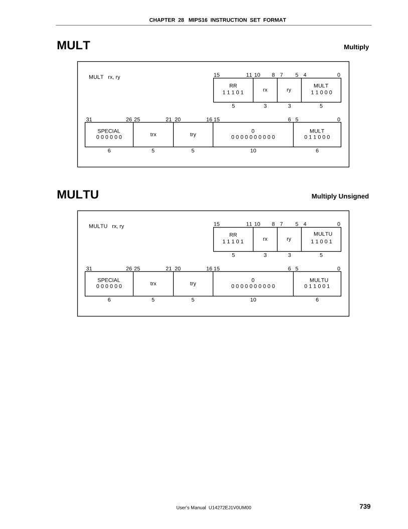
CHAPTER 28 MIPS16 INSTRUCTION SET FORMAT
User’s Manual U14272EJ1V0UM00 739
MULT Multiply
0561516 2021252631
6
04578101115
5
SPECIAL0 0 0 0 0 0 trx try
00 0 0 0 0 0 0 0 0 0
MULT0 1 1 0 0 0
10556
335
MULT1 1 0 0 0ryrx
RR1 1 1 0 1
MULT rx, ry
MULTU Multiply Unsigned
0561516 2021252631
6
04578101115
5
SPECIAL0 0 0 0 0 0 trx try
00 0 0 0 0 0 0 0 0 0
MULTU0 1 1 0 0 1
10556
335
MULTU1 1 0 0 1ryrx
RR1 1 1 0 1
MULTU rx, ry
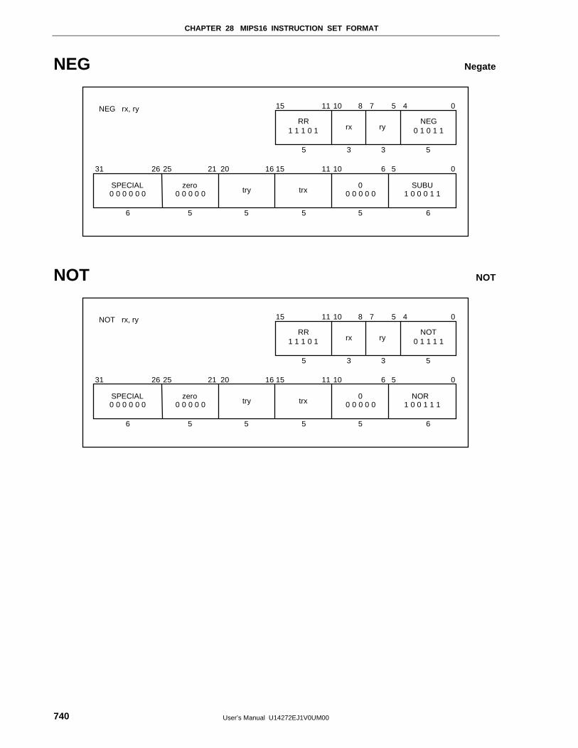
CHAPTER 28 MIPS16 INSTRUCTION SET FORMAT
User’s Manual U14272EJ1V0UM00740
NEG Negate
05610111516 20212631
6
04578101115
5
SPECIAL0 0 0 0 0 0
zero0 0 0 0 0 try trx
SUBU1 0 0 0 1 1
5556
335
NEG0 1 0 1 1ryrx
RR1 1 1 0 1
NEG rx, ry
00 0 0 0 0
5
25
NOT NOT
05610111516 20212631
6
04578101115
5
SPECIAL0 0 0 0 0 0
zero0 0 0 0 0 try trx
NOR1 0 0 1 1 1
5556
335
NOT0 1 1 1 1ryrx
RR1 1 1 0 1
NOT rx, ry
00 0 0 0 0
5
25

CHAPTER 28 MIPS16 INSTRUCTION SET FORMAT
User’s Manual U14272EJ1V0UM00 741
OR OR
05610111516 20212631
6
04578101115
5
SPECIAL0 0 0 0 0 0 trx try trx
OR1 0 0 1 0 1
5556
335
OR0 1 1 0 1ryrx
RR1 1 1 0 1
OR rx, ry
00 0 0 0 0
5
25
SB Store Byte
0451516 2021252631
5
04578101115
5
SB1 0 1 0 0 0 trx try
00 0 0 0 0 0 0 0 0 00
immediate
11556
335
immediateryrxSB
1 1 0 0 0
SB ry, offset (rx)
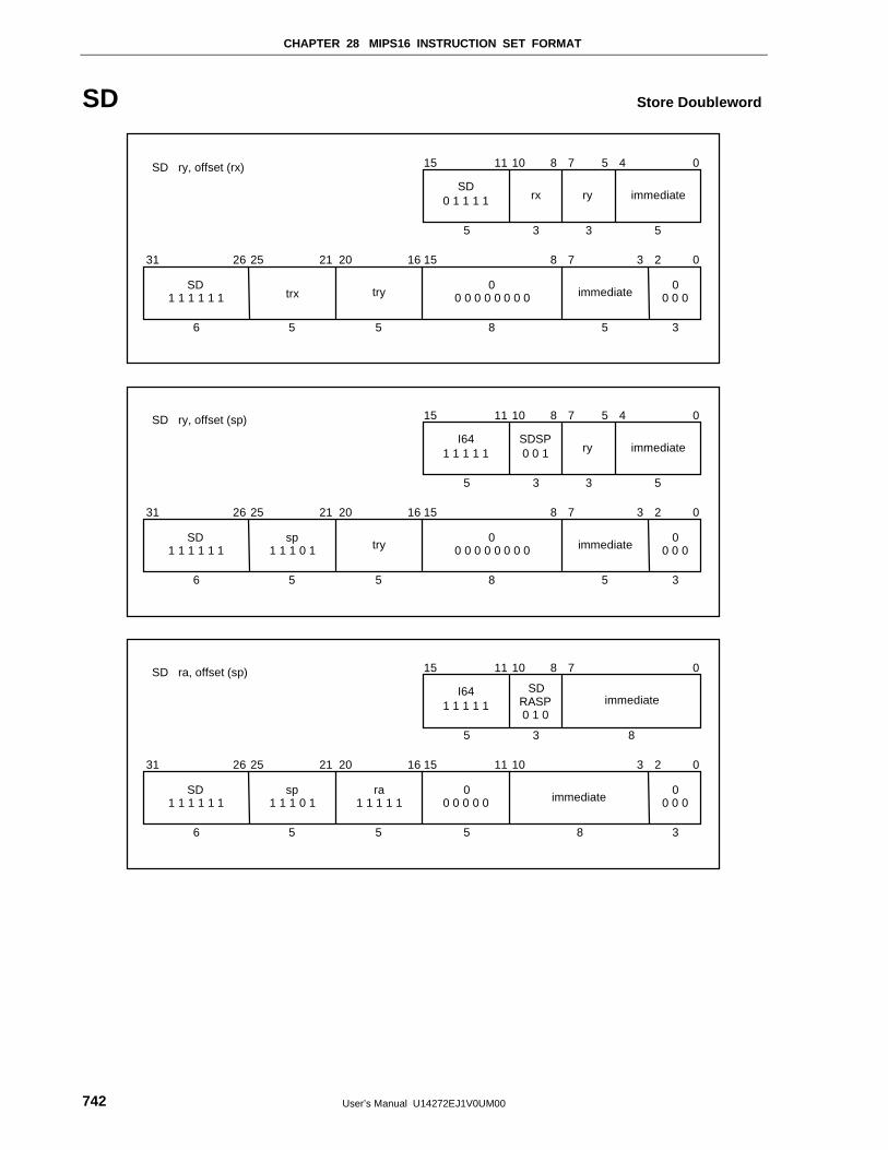
CHAPTER 28 MIPS16 INSTRUCTION SET FORMAT
User’s Manual U14272EJ1V0UM00742
SD Store Doubleword
023781516 2021252631
5
04578101115
5
SD1 1 1 1 1 1 trx try
00 0 0 0 0 0 0 0 immediate
8556
335
immediateryrxSD
0 1 1 1 1
SD ry, offset (rx)
3
00 0 0
023781516 2021252631
5
04578101115
5
SD1 1 1 1 1 1
sp1 1 1 0 1 try
00 0 0 0 0 0 0 0 immediate
8556
335
immediaterySDSP0 0 1
I641 1 1 1 1
SD ry, offset (sp)
3
00 0 0
02310111516 2021252631
8
078101115
8
SD1 1 1 1 1 1
sp1 1 1 0 1
ra1 1 1 1 1
00 0 0 0 0 immediate
5556
35
immediateSD
RASP0 1 0
I641 1 1 1 1
SD ra, offset (sp)
00 0 0
3
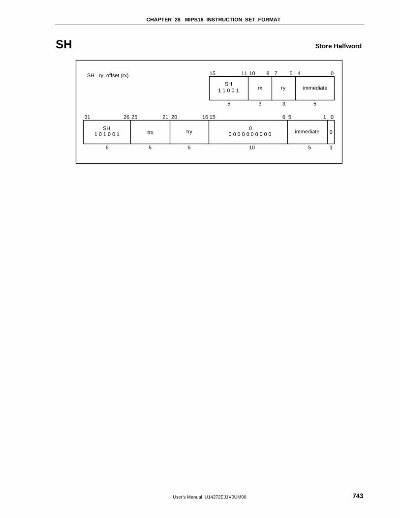
CHAPTER 28 MIPS16 INSTRUCTION SET FORMAT
User’s Manual U14272EJ1V0UM00 743
SH Store Halfword
01561516 2021252631
5
04578101115
5
SH1 0 1 0 0 1 trx try
00 0 0 0 0 0 0 0 0 0 immediate
10556
335
immediateryrxSH
1 1 0 0 1
SH ry, offset (rx)
1
0
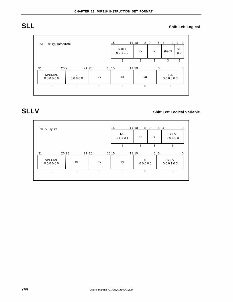
CHAPTER 28 MIPS16 INSTRUCTION SET FORMAT
User’s Manual U14272EJ1V0UM00744
SLL Shift Left Logical
05610111516 2021252631
6
1 024578101115
3
SPECIAL0 0 0 0 0 0
00 0 0 0 0 try sa
SLL0 0 0 0 0 0
5556
335
SLL0 0rxry
SHIFT0 0 1 1 0
SLL rx, ry, immediate
shamt
2
trx
5
SLLV Shift Left Logical Variable
05610111516 20212631
6
04578101115
5
SPECIAL0 0 0 0 0 0 trx try try
SLLV0 0 0 1 0 0
5556
335
SLLV0 0 1 0 0ryrx
RR1 1 1 0 1
SLLV ry, rx
00 0 0 0 0
5
25
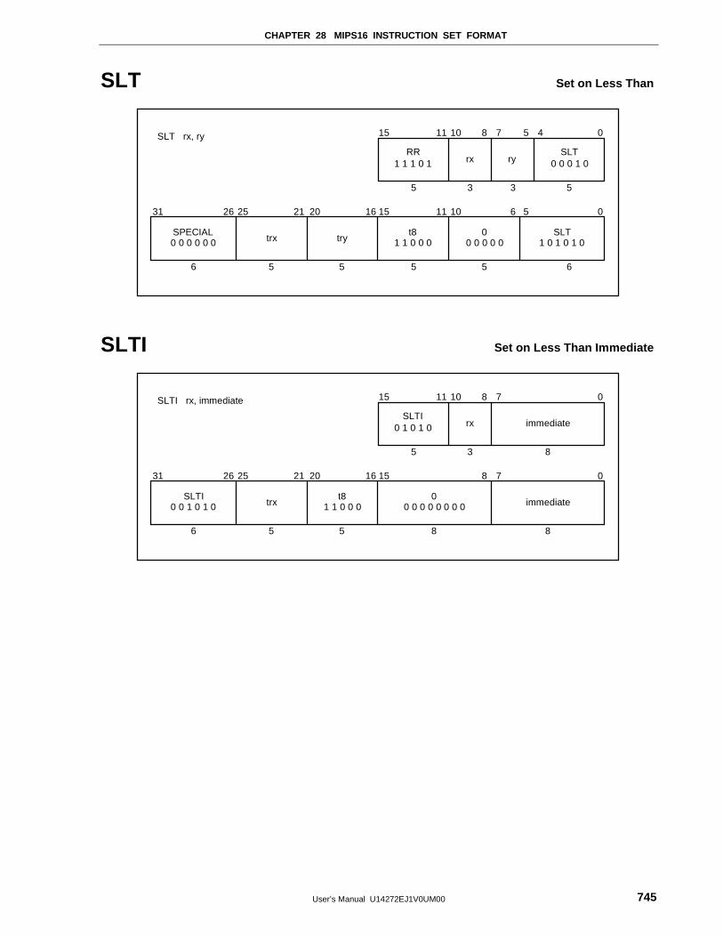
CHAPTER 28 MIPS16 INSTRUCTION SET FORMAT
User’s Manual U14272EJ1V0UM00 745
SLT Set on Less Than
05610111516 20212631
6
04578101115
5
SPECIAL0 0 0 0 0 0 trx try
t81 1 0 0 0
SLT1 0 1 0 1 0
5556
335
SLT0 0 0 1 0ryrx
RR1 1 1 0 1
SLT rx, ry
00 0 0 0 0
5
25
SLTI Set on Less Than Immediate
0781516 2021252631
8
078101115
8
SLTI0 0 1 0 1 0 trx
t81 1 0 0 0
00 0 0 0 0 0 0 0 immediate
8556
35
immediaterxSLTI
0 1 0 1 0
SLTI rx, immediate
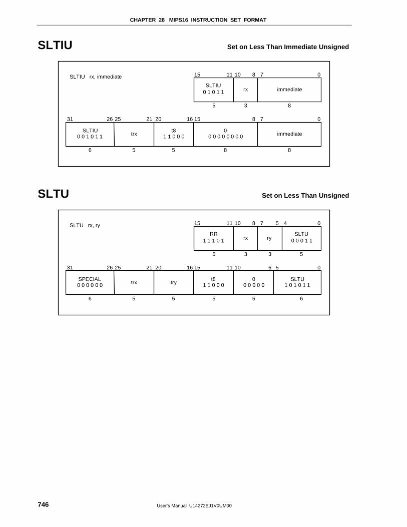
CHAPTER 28 MIPS16 INSTRUCTION SET FORMAT
User’s Manual U14272EJ1V0UM00746
SLTIU Set on Less Than Immediate Unsigned
0781516 2021252631
8
078101115
8
SLTIU0 0 1 0 1 1 trx
t81 1 0 0 0
00 0 0 0 0 0 0 0 immediate
8556
35
immediaterxSLTIU
0 1 0 1 1
SLTIU rx, immediate
SLTU Set on Less Than Unsigned
05610111516 20212631
6
04578101115
5
SPECIAL0 0 0 0 0 0 trx try
t81 1 0 0 0
SLTU1 0 1 0 1 1
5556
335
SLTU0 0 0 1 1ryrx
RR1 1 1 0 1
SLTU rx, ry
00 0 0 0 0
5
25
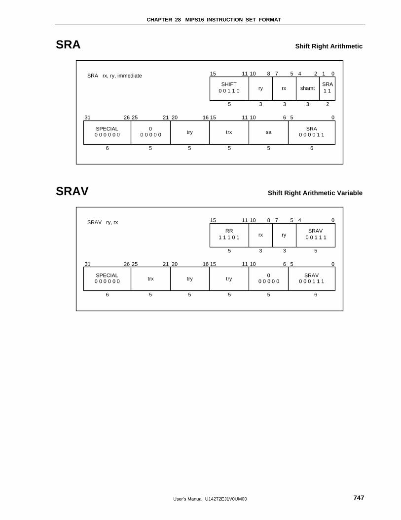
CHAPTER 28 MIPS16 INSTRUCTION SET FORMAT
User’s Manual U14272EJ1V0UM00 747
SRA Shift Right Arithmetic
05610111516 2021252631
6
1 024578101115
3
SPECIAL0 0 0 0 0 0
00 0 0 0 0 try sa
SRA0 0 0 0 1 1
5556
335
SRA1 1rxry
SHIFT0 0 1 1 0
SRA rx, ry, immediate
shamt
2
trx
5
SRAV Shift Right Arithmetic Variable
05610111516 20212631
6
04578101115
5
SPECIAL0 0 0 0 0 0 trx try try
SRAV0 0 0 1 1 1
5556
335
SRAV0 0 1 1 1ryrx
RR1 1 1 0 1
SRAV ry, rx
00 0 0 0 0
5
25
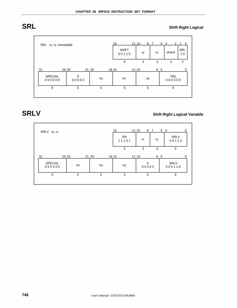
CHAPTER 28 MIPS16 INSTRUCTION SET FORMAT
User’s Manual U14272EJ1V0UM00748
SRL Shift Right Logical
05610111516 2021252631
6
1 024578101115
3
SPECIAL0 0 0 0 0 0
00 0 0 0 0 try sa
SRL0 0 0 0 0 0
5556
335
SRL1 0rxry
SHIFT0 0 1 1 0
SRL rx, ry, immediate
shamt
2
trx
5
SRLV Shift Right Logical Variable
05610111516 20212631
6
04578101115
5
SPECIAL0 0 0 0 0 0 trx try try
SRLV0 0 0 1 1 0
5556
335
SRLV0 0 1 1 0ryrx
RR1 1 1 0 1
SRLV ry, rx
00 0 0 0 0
5
25
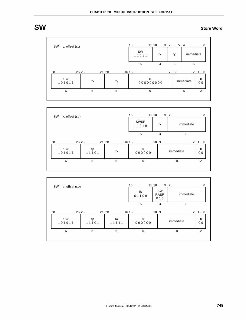
CHAPTER 28 MIPS16 INSTRUCTION SET FORMAT
User’s Manual U14272EJ1V0UM00 749
SW Store Word
1 02671516 2021252631
5
04578101115
5
SW1 0 1 0 1 1 trx try
00 0 0 0 0 0 0 0 0 immediate
9556
335
immediateryrxSW
1 1 0 1 1
SW ry, offset (rx)
00 0
2
1 021516 2021252631
8
078101115
8
SW1 0 1 0 1 1
sp1 1 1 0 1 trx
00 0 0 0 0 0 immediate
6556
35
immediaterxSWSP
1 1 0 1 0
SW rx, offset (sp)
00 0
2
910
1 021516 2021252631
8
078101115
8
SW1 0 1 0 1 1
sp1 1 1 0 1
ra1 1 1 1 1
00 0 0 0 0 0 immediate
6556
35
immediateSW
RASP0 1 0
I80 1 1 0 0
SW ra, offset (sp)
00 0
2
910
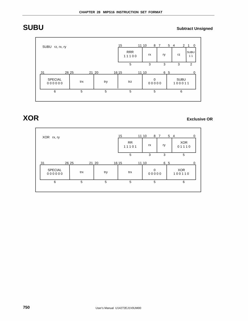
CHAPTER 28 MIPS16 INSTRUCTION SET FORMAT
User’s Manual U14272EJ1V0UM00750
SUBU Subtract Unsigned
05610111516 2021252631
6
1 024578101115
3
SPECIAL0 0 0 0 0 0 trx try
00 0 0 0 0
SUBU1 0 0 0 1 1
5556
335
SUBU1 1ryrx
RRR1 1 1 0 0
SUBU rz, rx, ry
rz
2
trz
5
XOR Exclusive OR
05610111516 20212631
6
04578101115
5
SPECIAL0 0 0 0 0 0 trx try trx
XOR1 0 0 1 1 0
5556
335
XOR0 1 1 1 0ryrx
RR1 1 1 0 1
XOR rx, ry
00 0 0 0 0
5
25
User’s Manual U14272EJ1V0UM00 751
CHAPTER 29 VR4181 COPROCESSOR 0 HAZARDS
The VR4110 CPU core avoids contention of its internal resources by causing a pipeline interlock in such cases as
when the contents of the destination register of an instruction are used as a source in the succeeding instruction.
Therefore, instructions such as NOP must not be inserted between instructions.
However, interlocks do not occur on the operations related to the CP0 registers and the TLB. Therefore,
contention of internal resources should be considered when composing a program that manipulates the CP0
registers or the TLB. The CP0 hazards define the number of NOP instructions that is required to avoid contention of
internal resources, or the number of instructions unrelated to contention. This chapter describes the CP0 hazards.
The CP0 hazards of the VR4110 CPU core are as or less stringent than those of the VR4000. Table 30-1 lists the
Coprocessor 0 hazards of the VR4110 CPU core. Code that complies with these hazards will run without modification
on the VR4000.
The contents of the CP0 registers or the bits in the “Source” column of this table can be used as a source after
they are fixed.
The contents of the CP0 registers or the bits in the “Destination” column of this table can be available as a
destination after they are stored.
Based on this table, the number of NOP instructions required between instructions related to the TLB is computed
by the following formula, and so is the number of instructions unrelated to contention:
(Destination Hazard number of A) – [(Source Hazard number of B) + 1]
As an example, to compute the number of instructions required between an MTC0 and a subsequent MFC0
instruction, this is:
(5) – (3 + 1) = 1 instruction
The CP0 hazards do not generate interlocks of pipeline. Therefore, the required number of instruction must be
controlled by program.
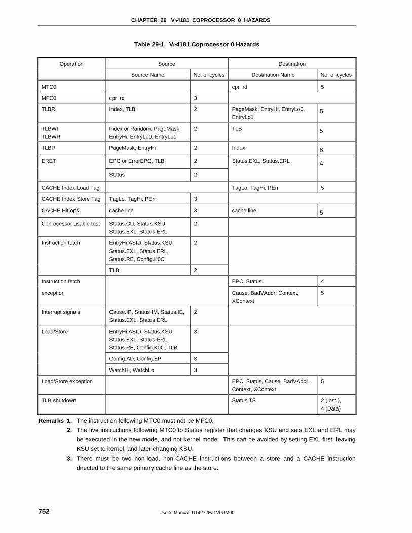
CHAPTER 29 VR4181 COPROCESSOR 0 HAZARDS
User’s Manual U14272EJ1V0UM00752
Table 29-1. VR4181 Coprocessor 0 Hazards
Operation Source Destination
Source Name No. of cycles Destination Name No. of cycles
MTC0 cpr rd 5
MFC0 cpr rd 3
TLBR Index, TLB 2 PageMask, EntryHi, EntryLo0,
EntryLo15
TLBWI
TLBWR
Index or Random, PageMask,
EntryHi, EntryLo0, EntryLo1
2 TLB 5
TLBP PageMask, EntryHi 2 Index 6
ERET EPC or ErrorEPC, TLB 2 Status.EXL, Status.ERL 4
Status 2
CACHE Index Load Tag TagLo, TagHi, PErr 5
CACHE Index Store Tag TagLo, TagHi, PErr 3
CACHE Hit ops. cache line 3 cache line 5
Coprocessor usable test Status.CU, Status.KSU,
Status.EXL, Status.ERL
2
Instruction fetch EntryHi.ASID, Status.KSU,
Status.EXL, Status.ERL,
Status.RE, Config.K0C
2
TLB 2
Instruction fetch EPC, Status 4
exception Cause, BadVAddr, Context,
XContext
5
Interrupt signals Cause.IP, Status.IM, Status.IE,
Status.EXL, Status.ERL
2
Load/Store EntryHi.ASID, Status.KSU,
Status.EXL, Status.ERL,
Status.RE, Config.K0C, TLB
3
Config.AD, Config.EP 3
WatchHi, WatchLo 3
Load/Store exception EPC, Status, Cause, BadVAddr,
Context, XContext
5
TLB shutdown Status.TS 2 (Inst.),
4 (Data)
Remarks 1. The instruction following MTC0 must not be MFC0.
2. The five instructions following MTC0 to Status register that changes KSU and sets EXL and ERL may
be executed in the new mode, and not kernel mode. This can be avoided by setting EXL first, leaving
KSU set to kernel, and later changing KSU.
3. There must be two non-load, non-CACHE instructions between a store and a CACHE instruction
directed to the same primary cache line as the store.
CHAPTER 29 VR4181 COPROCESSOR 0 HAZARDS
User’s Manual U14272EJ1V0UM00 753
Cautions 1. If the setting of the K0 bit in the Config register is changed to uncached mode by MTC0, the
accessed memory area is switched to the uncached one at the instruction fetch of the third
instruction after MTC0.
2. A stall of several instructions occurs if a jump or branch instruction is executed immediately
after the setting of the ITS bit in the Status register.
The status during execution of the following instruction for which CP0 hazards must be considered is described
below.
(1) MTC0
Destination: The completion of writing to a destination register (CP0) of MTC0.
(2) MFC0
Source: The confirmation of a source register (CP0) of MFC0.
(3) TLBR
Source: The confirmation of the status of TLB and the Index register before the execution of TLBR.
Destination: The completion of writing to a destination register (CP0) of TLBR.
(4) TLBWI, TLBWR
Source: The confirmation of a source register of these instructions and registers used to specify a TLB
entry.
Destination: The completion of writing to TLB by these instructions.
(5) TLBP
Source: The confirmation of the PageMask register and the EntryHi register before the execution of TLBP.
Destination: The completion of writing the result of execution of TLBP to the Index register.
(6) ERET
Source: The confirmation of registers containing information necessary for executing ERET.
Destination: The completion of the processor state transition by the execution of ERET.
(7) CACHE Index Load Tag
Destination: The completion of writing the results of execution of this instruction to the related registers.
CHAPTER 29 VR4181 COPROCESSOR 0 HAZARDS
User’s Manual U14272EJ1V0UM00754
(8) CACHE Index Store Tag
Source: The confirmation of registers containing information necessary for executing this instruction.
(9) Coprocessor Usable Test
Source: The confirmation of modes set by the bits of the CP0 registers in the “Source” column.
Examples 1. When accessing the CP0 registers in User mode after the contents of the CU0 bit of the Status
register are modified, or when executing an instruction such as TLB instructions, CACHE
instructions, or branch instructions that use the resource of the CP0.
2. When accessing the CP0 registers in the operating mode set in the Status register after the KSU,
EXL, and ERL bits of the Status register are modified.
(10) Instruction Fetch
Source: The confirmation of the operating mode and TLB necessary for instruction fetch.
Examples 1. When changing the operating mode from User to Kernel and fetching instructions after the KSU,
EXL, and ERL bits of the Status register are modified.
2. When fetching instructions using the modified TLB entry after TLB modification.
(11) Instruction Fetch Exception
Destination: The completion of writing to registers containing information related to the exception when an
exception occurs on instruction fetch.
(12) Interrupts
Source: The confirmation of registers judging the condition of occurrence of interrupt when an interrupt
factor is detected.
(13)Loads/Sores
Source: The confirmation of the operating mode related to the address generation of Load/Store
instructions, TLB entries, the cache mode set in the K0 bit of the Config register, and the registers
setting the condition of occurrence of a Watch exception.
Example When Loads/Stores are executed in the kernel field after changing the mode from User to Kernel.
(14)Load/Store Exception
Destination: The completion of writing to registers containing information related to the exception when an
exception occurs on load or store operation.
(15)TLB Shutdown
Destination: The completion of writing to the TS bit of the Status register when a TLB shutdown occurs.
CHAPTER 29 VR4181 COPROCESSOR 0 HAZARDS
User’s Manual U14272EJ1V0UM00 755
Table 29-2 indicates examples of calculation.
Table 29-2. Calculation Example of CP0 Hazard and Number of Instructions Inserted
Destination Source
Contending
internal
resource
Number of
instructions
inserted
Formula
TLBWR/TLBWI TLBP TLB Entry 2 5 – (2 + 1)
TLBWR/TLBWI Load or Store using newly modified TLB TLB Entry 1 5 – (3 + 1)
TLBWR/TLBWI Instruction fetch using newly modified TLB TLB Entry 2 5 – (2 + 1)
MTC0, Status [CU] Coprocessor instruction that requires the setting
of CU
Status [CU] 2 5 – (2 + 1)
TLBR MFC0 EntryHi EntryHi 1 5 – (3 + 1)
MTC0 EntryLo0 TLBWR/TLBWI EntryLo0 2 5 – (2 + 1)
TLBP MFC0 Index Index 2 6 – (3 + 1)
MTC0 EntryHi TLBP EntryHi 2 5 – (2 + 1)
MTC0 EPC ERET EPC 2 5 – (2 + 1)
MTC0 Status ERET Status 2 5 – (2 + 1)
MTC0 Status [IE] Note Instruction that causes an interrupt Status [IE] 2 5 – (2 + 1)
Note The number of hazards is undefined if the instruction execution sequence is changed by exceptions. In
such a case, the minimum number of hazards until the IE bit value is confirmed may be the same as the
maximum number of hazards until an interrupt request occurs that is pending and enabled.

User’s Manual U14272EJ1V0UM00756
[MEMO]
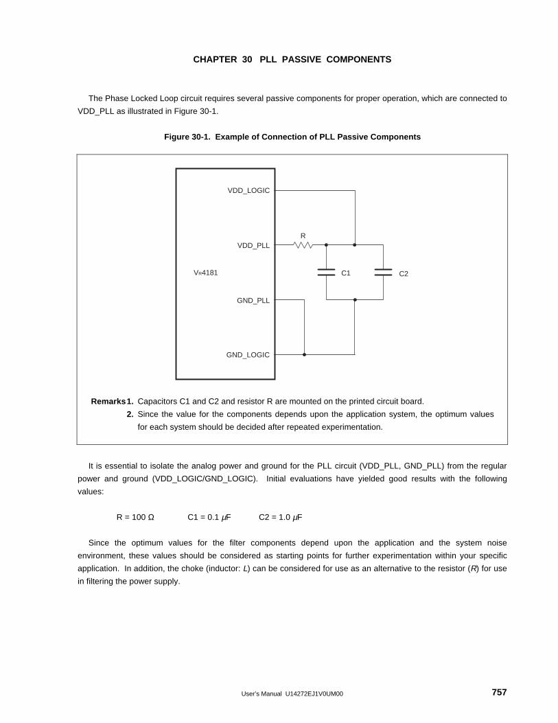
User’s Manual U14272EJ1V0UM00 757
CHAPTER 30 PLL PASSIVE COMPONENTS
The Phase Locked Loop circuit requires several passive components for proper operation, which are connected to
VDD_PLL as illustrated in Figure 30-1.
Figure 30-1. Example of Connection of PLL Passive Components
VDD_LOGIC
VDD_PLL
GND_LOGIC
VR4181
R
C1 C2
GND_PLL
Remarks1. Capacitors C1 and C2 and resistor R are mounted on the printed circuit board.
2. Since the value for the components depends upon the application system, the optimum values
for each system should be decided after repeated experimentation.
It is essential to isolate the analog power and ground for the PLL circuit (VDD_PLL, GND_PLL) from the regular
power and ground (VDD_LOGIC/GND_LOGIC). Initial evaluations have yielded good results with the following
values:
R = 100 Ω C1 = 0.1 µF C2 = 1.0 µF
Since the optimum values for the filter components depend upon the application and the system noise
environment, these values should be considered as starting points for further experimentation within your specific
application. In addition, the choke (inductor: L) can be considered for use as an alternative to the resistor (R) for use
in filtering the power supply.

User’s Manual U14272EJ1V0UM00758
[MEMO]
Although NEC has taken all possible stepsto ensure that the documentation suppliedto our customers is complete, bug freeand up-to-date, we readily accept thaterrors may occur. Despite all the care andprecautions we've taken, you mayencounter problems in the documentation.Please complete this form wheneveryou'd like to report errors or suggestimprovements to us.
Hong Kong, Philippines, OceaniaNEC Electronics Hong Kong Ltd.Fax: +852-2886-9022/9044
KoreaNEC Electronics Hong Kong Ltd.Seoul BranchFax: 02-528-4411
TaiwanNEC Electronics Taiwan Ltd.Fax: 02-2719-5951
Address
North AmericaNEC Electronics Inc.Corporate Communications Dept.Fax: 1-800-729-9288
1-408-588-6130
EuropeNEC Electronics (Europe) GmbHTechnical Documentation Dept.Fax: +49-211-6503-274
South AmericaNEC do Brasil S.A.Fax: +55-11-6462-6829
Asian Nations except PhilippinesNEC Electronics Singapore Pte. Ltd.Fax: +65-250-3583
JapanNEC Semiconductor Technical HotlineFax: 044-435-9608
I would like to report the following error/make the following suggestion:
Document title:
Document number: Page number:
Thank you for your kind support.
If possible, please fax the referenced page or drawing.
Excellent Good Acceptable PoorDocument Rating
Clarity
Technical Accuracy
Organization
CS 00.6
Name
Company
From:
Tel. FAX
Facsimile Message