Embed Size (px)
Citation preview
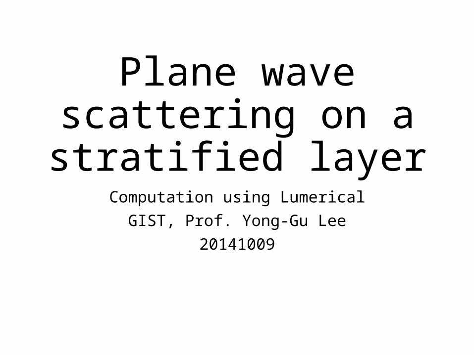
Plane wave scatter-ing on a stratified
layerComputation using Lumerical
GIST, Prof. Yong-Gu Lee20141009
Objective
• 100nm thick gold layer is illuminated with a plane wave @1070nm p-polarized in the orthogonal di-rection. Compute the total electric field distribu-tion.
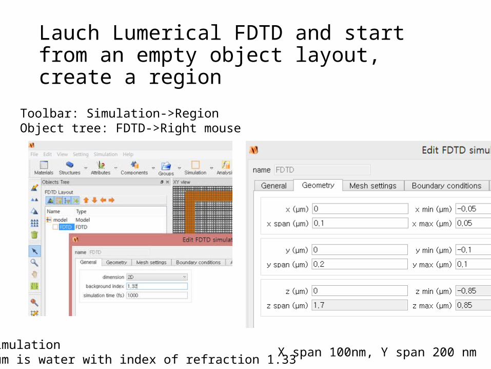
Lauch Lumerical FDTD and start from an empty object layout, create a re-gion
Toolbar: Simulation->RegionObject tree: FDTD->Right mouse
2D simulationMedium is water with index of refraction 1.33 X span 100nm, Y span 200 nm

Create a mesh of particular width and depth
Toolbar: Simulation->MeshObject tree: mesh->Right mouse
X span 100nm, Y span 200 nm
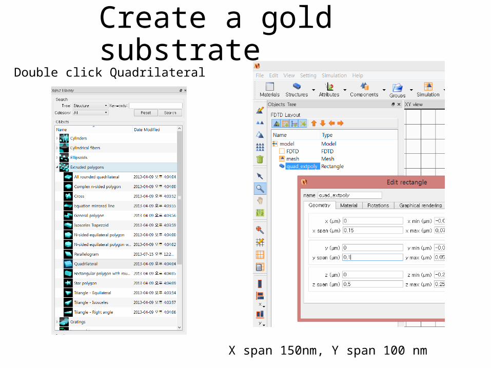
Double click Quadrilateral
X span 150nm, Y span 100 nm
Create a gold substrate
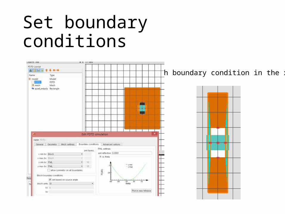
Set boundary conditions
Bloch boundary condition in the x-axis
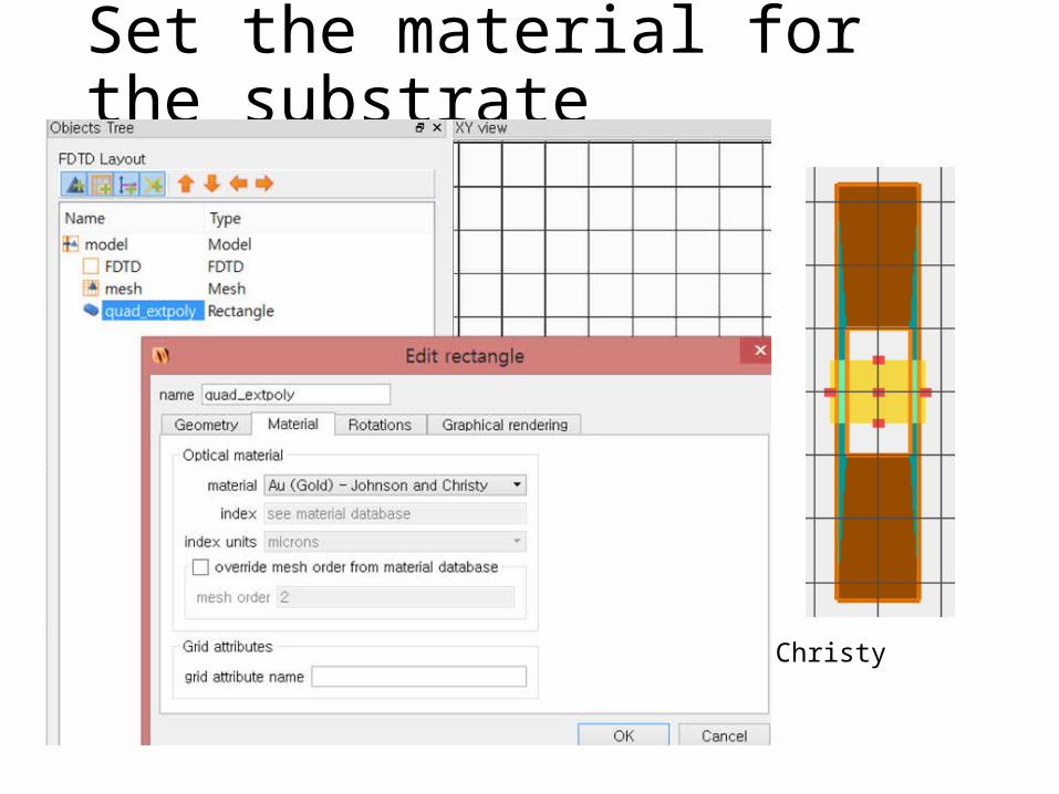
Set the material for the substrate
Au (Gold) – Johnson and Christy
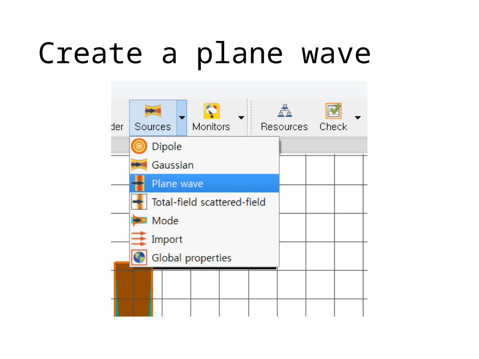
Create a plane wave
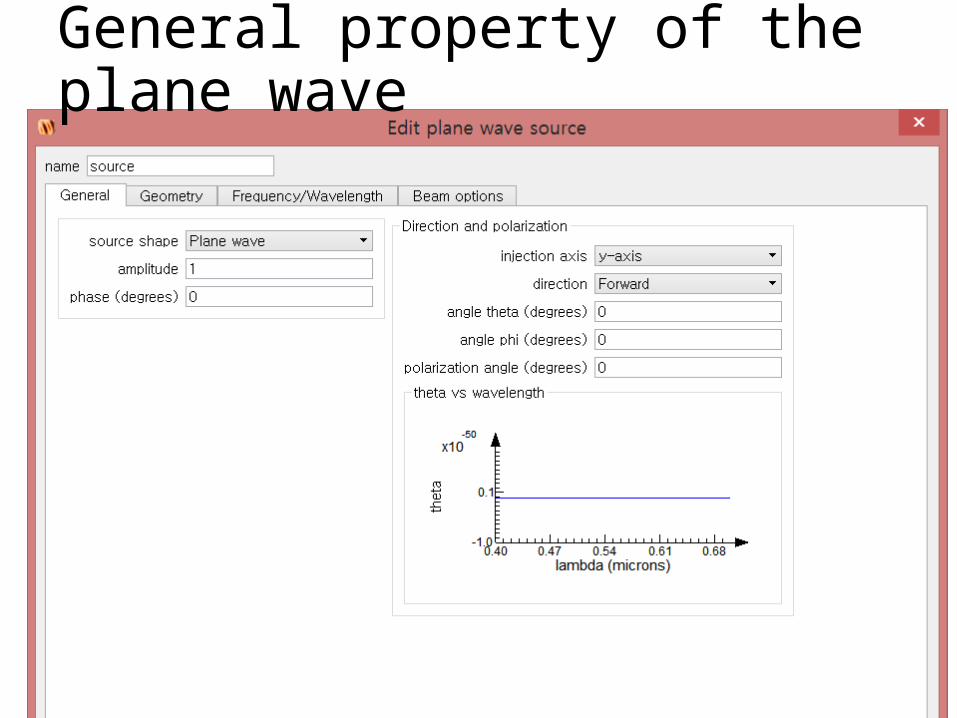
General property of the plane wave
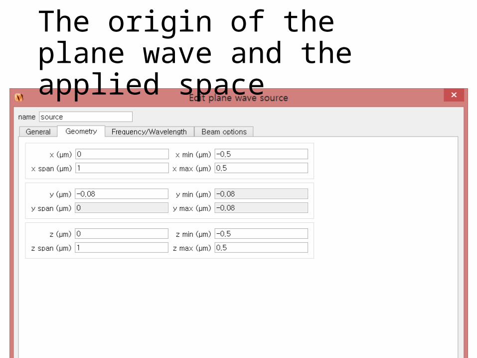
The origin of the plane wave and the applied space
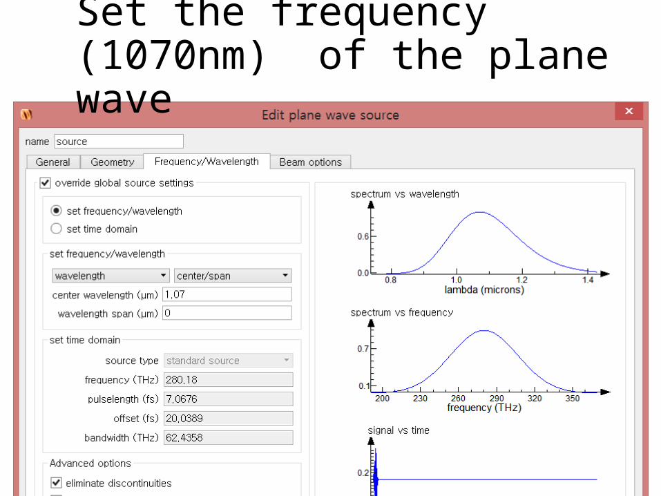
Set the frequency (1070nm) of the plane wave
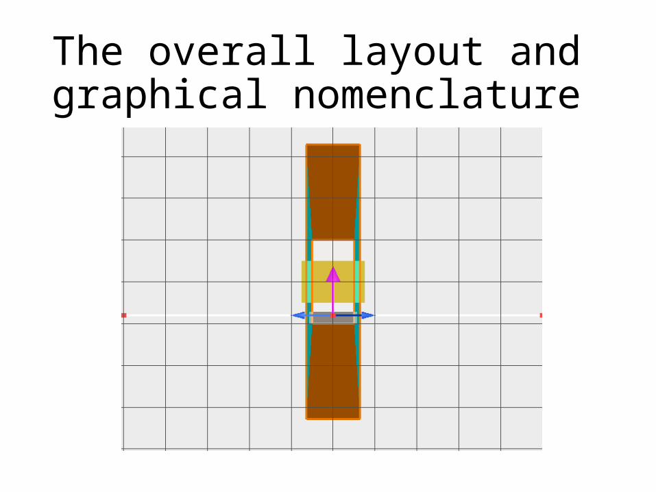
The overall layout and graphical nomenclature
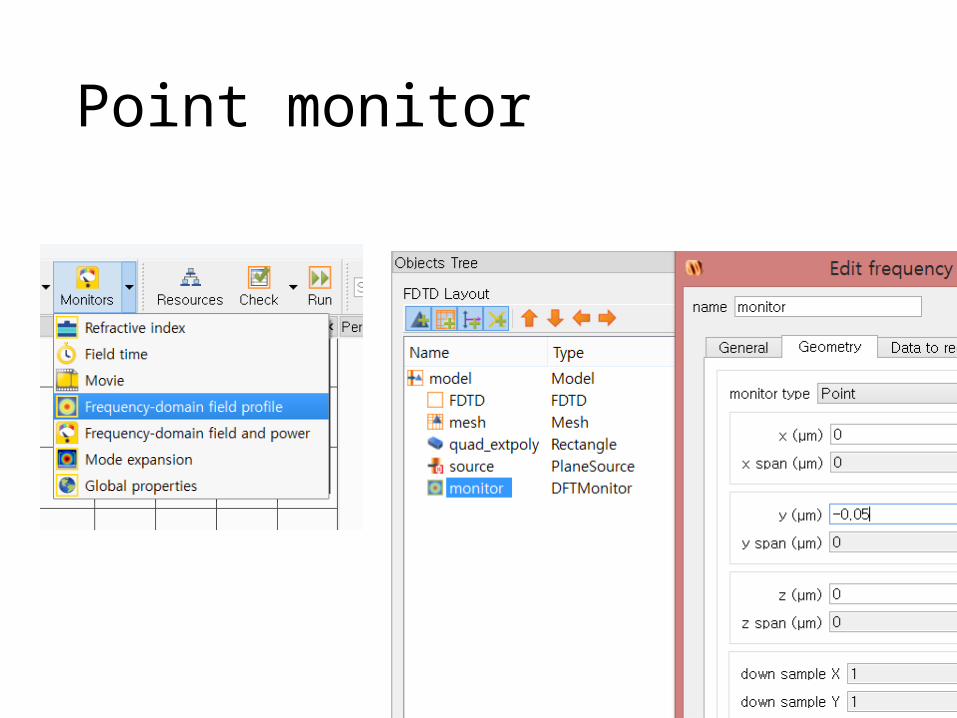
Point monitor
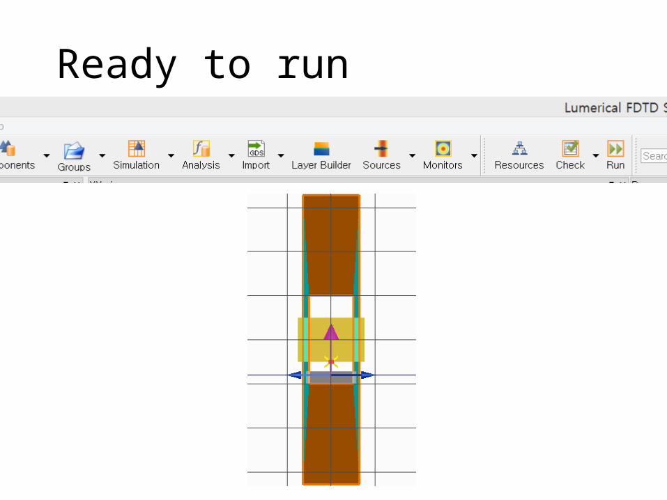
Ready to run
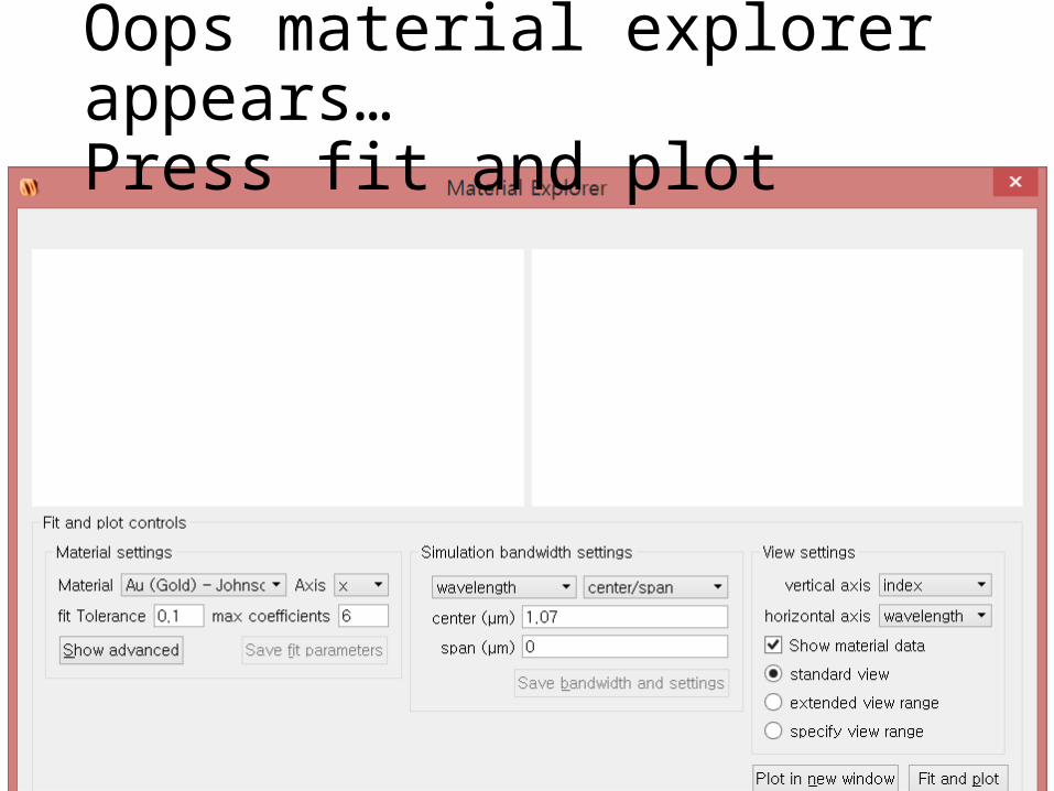
Oops material explorer ap-pears…Press fit and plot
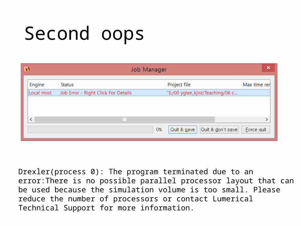
Drexler(process 0): The program terminated due to an error:There is no possible parallel processor layout that can be used because the simulation volume is too small. Please re-duce the number of processors or contact Lumerical Technical Support for more informa-tion.
Second oops
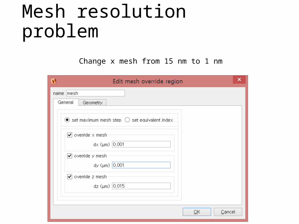
Change x mesh from 15 nm to 1 nm
Mesh resolution problem
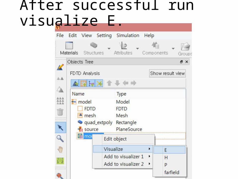
After successful run visual-ize E.
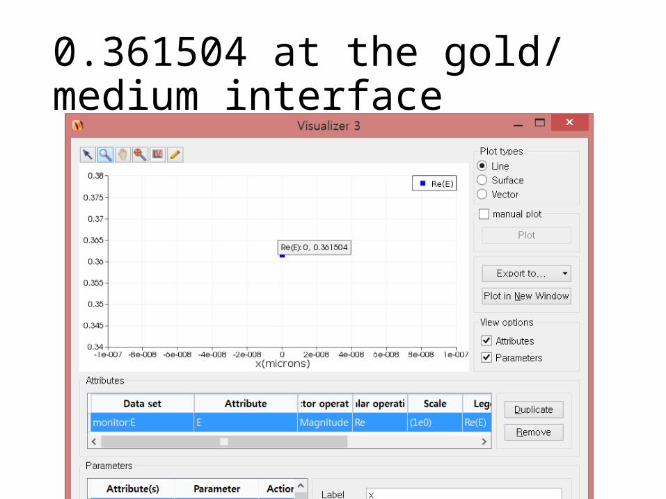
0.361504 at the gold/medium interface
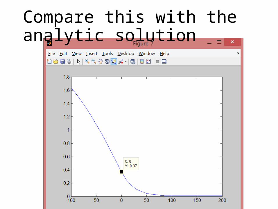
Compare this with the ana-lytic solution