Embed Size (px)
Citation preview
DYNAMIC ENGINEERING 150 DuBois, Suite C
Santa Cruz, CA 95060 (831) 457-8891 Fax (831) 457-4793
http://www.dyneng.com [email protected]
Est. 1988
User Manual
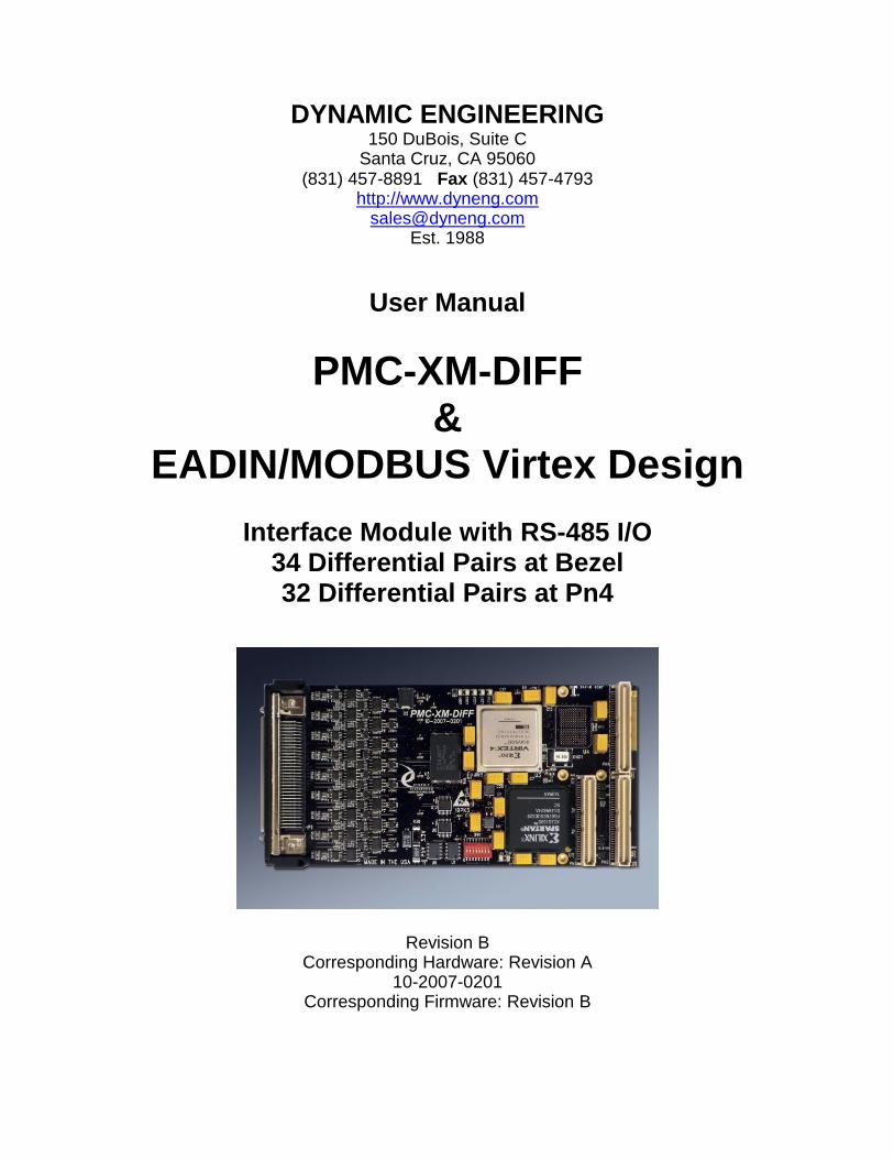
PMC-XM-DIFF &
EADIN/MODBUS Virtex Design
Interface Module with RS-485 I/O 34 Differential Pairs at Bezel 32 Differential Pairs at Pn4
Revision B Corresponding Hardware: Revision A
10-2007-0201 Corresponding Firmware: Revision B
Embedded Solutions Page 2 of 65
PMC-XM-EADIN/MODBUS PMC based interface module With RS-485 I/O hardware
Dynamic Engineering 150 DuBois, Suite C Santa Cruz, CA 95060 (831) 457-8891 FAX: (831) 457-4793
This document contains information of proprietary interest to Dynamic Engineering. It has been supplied in confidence and the recipient, by accepting this material, agrees that the subject matter will not be copied or reproduced, in whole or in part, nor its contents revealed in any manner or to any person except to meet the purpose for which it was delivered. Dynamic Engineering has made every effort to ensure that this manual is accurate and complete. Still, the company reserves the right to make improvements or changes in the product described in this document at any time and without notice. Furthermore, Dynamic Engineering assumes no liability arising out of the application or use of the device described herein. The electronic equipment described herein generates, uses, and can radiate radio frequency energy. Operation of this equipment in a residential area is likely to cause radio interference, in which case the user, at his own expense, will be required to take whatever measures may be required to correct the interference. Dynamic Engineering’s products are not authorized for use as critical components in life support devices or systems without the express written approval of the president of Dynamic Engineering. Connection of incompatible hardware is likely to cause serious damage.
©2012-2013 by Dynamic Engineering. Other trademarks and registered trademarks are owned by their respective manufactures. Manual Revision B. Revised June 11, 2013
Embedded Solutions Page 3 of 65
Table of Contents
PRODUCT DESCRIPTION 6
THEORY OF OPERATION 8
PROGRAMMING 9
ADDRESS MAP SPARTAN3 10
Register Definitions 11 PMC_XM_BASE 11 PMC_XM_USER_SWITCH 13 XM_CHAN0/1_CNTRL 15 XM_CHAN0/1_STATUS 17 XM_CHAN0/1_WR/RD_DMA_PNTR 19 XM_CHAN0/1_FIFO 19 XM_CHAN0/1_TX_AMT_LVL 20 XM_CHAN0/1_RX_AFL_LVL 20 XM_CHAN0/1_TX/RX_FIFO_COUNT 21
EADIN/MODBUS VIRTEX DESIGN PRODUCT DESCRIPTION 22
EADIN/MODBUS VIRTEX DESIGN THEORY OF OPERATION 23
EADIN Protocol 23 Bulk Unicast Write 24 Bulk Unicast Read 26
Modbus Protocol 28 Read Multiple Registers – Command = 0x03 28 Write Multiple Registers – Command = 0x10 30 Read/Write Multiple Registers – Command = 0x17 33
ADDRESS MAP: PMC-XM-EADIN / MODBUS DESIGN 36
Register Definitions 39 XM_EN_MB_BASE 39 XM_EN_MB_ID 41 XM_EN_MB_START 41 XM_EN_MB_STOP 42 XM_EN_MB_POLY 42
Embedded Solutions Page 4 of 65
XM_EN_MB_CHAN0-31_CNTRL 43 XM_EN_MB_CHAN0-31_STATUS 45 XM_EN_MB_CHAN0-31_FF_CNTS 49 XM_EN_MB_CHAN0-31_CRC_TIMECOUNT 50 XM_EN_MB_CHAN0-31_FIFO 50
VIRTEX PIN OUT 51
PMC-XM-EN/MB FRONT PANEL IO PIN ASSIGNMENT 60
APPLICATIONS GUIDE 61
Interfacing 61
Construction and Reliability 62
Thermal Considerations 62
WARRANTY AND REPAIR 63
Service Policy 63 Out of Warranty Repairs 63
For Service Contact: 63
SPECIFICATIONS 64
ORDER INFORMATION 65
Embedded Solutions Page 5 of 65
List of Figures
FIGURE 1 PMC-XM-DIFF BLOCK DIAGRAM 6 FIGURE 2 PMC-XM SPARTAN3 XILINX ADDRESS MAP 10 FIGURE 3 PMC-XM SPARTAN3 BASE CONTROL REGISTER 11 FIGURE 4 PMC-XM SPARTAN3 USER SWITCH PORT 13 FIGURE 5 PMC-XM SPARTAN3 STATUS REGISTER 14 FIGURE 6 PMC-XM SPARTAN3 CHANNEL CONTROL REGISTER 15 FIGURE 7 PMC-XM SPARTAN3 CHANNEL STATUS REGISTER 17 FIGURE 8 PMC-XM SPARTAN3 CHANNEL DMA POINTER REGISTER 19 FIGURE 9 PMC-XM SPARTAN3 CHANNEL FIFO PORT 19 FIGURE 10 PMC-XM SPARTAN3 CHANNEL TX ALMOST EMPTY REGISTER 20 FIGURE 11 PMC-XM SPARTAN3 CHANNEL RX ALMOST FULL REGISTER 20 FIGURE 12 PMC-XM SPARTAN3 CHANNEL TX/RX FIFO COUNT PORT 21 FIGURE 13 PMC-XM-EN/MB EADIN BULK UNICAST WRITE FRAME 24 FIGURE 14 PMC-XM-EN/MB EADIN WRITE COMMAND FIFO FORMATS 24 FIGURE 14 (CONTINUED) PMC-XM-EN/MB EADIN WRITE COMMAND FIFO FORMATS 25 FIGURE 15 PMC-XM-EN/MB EADIN BULK UNICAST READ FRAME 26 FIGURE 16 PMC-XM-EN/MB EADIN READ COMMAND FIFO FORMATS 26 FIGURE 16 (CONTINUED) PMC-XM-EN/MB EADIN READ COMMAND FIFO FORMATS 27 FIGURE 17 PMC-XM-EN/MB MODBUS READ FRAME 28 FIGURE 18 PMC-XM-EN/MB MODBUS READ COMMAND FIFO FORMATS 29 FIGURE 19 PMC-XM-EN/MB MODBUS WRITE FRAME 30 FIGURE 20 PMC-XM-EN/MB MODBUS WRITE COMMAND FIFO FORMATS 31 FIGURE 20 (CONTINUED) PMC-XM-EN/MB MODBUS WRITE COMMAND FIFO FORMATS 32 FIGURE 21 PMC-XM-EN/MB MODBUS READ/WRITE FRAME 33 FIGURE 22 PMC-XM-EN/MB MODBUS RD/WR COMMAND FIFO FORMATS 34 FIGURE 22 (CONTINUED) PMC-XM-EN/MB MODBUS RD/WR COMMAND FIFO FORMATS 35 FIGURE 23 PMC-XM-EN/MB VIRTEX ADDRESS MAP 36 FIGURE 23 (CONTINUED) PMC-XM-EN/MB VIRTEX ADDRESS MAP 37 FIGURE 23 (CONTINUED) PMC-XM-EN/MB VIRTEX ADDRESS MAP 38 FIGURE 24 PMC-XM-EN/MB VIRTEX BASE CONTROL REGISTER 39 FIGURE 25 PMC-XM-EN/MB VIRTEX ID REGISTER 41 FIGURE 26 PMC-XM-EN/MB VIRTEX CHANNEL START 41 FIGURE 27 PMC-XM-EN/MB VIRTEX CHANNEL STOP 42 FIGURE 28 PMC-XM-EN/MB VIRTEX CRC POLYNOMIALS 42 FIGURE 29 PMC-XM-EN/MB VIRTEX CHANNEL CONTROL REGISTER 43 FIGURE 30 PMC-XM-EN/MB VIRTEX CHANNEL STATUS REGISTER 45 FIGURE 31 PMC-XM-EN/MB VIRTEX CHANNEL FIFO COUNTS PORT 49 FIGURE 32 PMC-XM-EN/MB VIRTEX CHANNEL CRC/TIMEOUT PORT 50 FIGURE 33 PMC-XM-EN/MB VIRTEX CHANNEL FIFO DATA PORT 50 FIGURE 34 PMC-XM-EN/MB FRONT PANEL INTERFACE 60
Embedded Solutions Page 6 of 65
Product Description
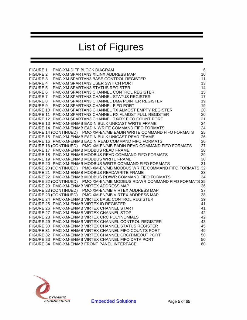
The PMC-XM-DIFF features a Xilinx Spartan3-2000 676 pin FPGA to implement the PCI interface and two independent I/O channels each with a separate input and output scatter-gather DMA engine to move data to/from host memory over the local 32-bit 33 MHz PCI bus. A Xilinx Virtex4 668 pin FPGA interfaces between the Spartan3 and the IO. The IO can be configured with RS-485, LVDS or a mixture of both. Each IO has separate direction, and termination controls to allow any combination of inputs and outputs. Impedance controlled and length matched within the mil [.001”] to allow for any user requirement. Other features include on-board PLL, optional RAM (1Mx36-bit QDDRII RAM), temperature sensor, DIP Switch, Built in DMA, and user LED’s.
PCI IF
Data Flow
Control
FPGA
1M x 36 RAM
DMA
RX TX
4K
x32
FIF
O
4K
x32
FIF
O
RX TX
4K
x32
FIF
O
4K
x32
FIF
O
User Virtex PLL
34 LVDS / RS-485 IO
Programmable TerminationsLEDs(4)
DIP
SW
ITC
H
TEMP
SENSOR
FIGURE 1 PMC-XM-DIFF BLOCK DIAGRAM
The engineering kit comes with a basic design for the Virtex consisting of the VHDL package used to generate the ATP implementation. The design includes decoding, DMA, two channels, IO loop-back and more. The package can include the Windows® driver and reference code. The reference software is provided as source and can be user modified to do whatever you want.

Embedded Solutions Page 7 of 65
The package includes an auto design detection feature to automatically load menus corresponding to different designs loaded into the Virtex. The user can change the design number and use the generic driver to access new features added to the client’s implementation. The Virtex can be loaded from FLASH and overwritten with software. The reference package includes the Virtex load utilities, PLL programming software, and Temperature sensor read as well as IO loop-back tests. Multiple Virtex designs can be implemented as bit-files and loaded into the Virtex at any time without powering-down the system. The Dynamic Engineering drivers for the PMC-XM-Diff can load any specified bit-file and will automatically unload the current Virtex driver and load a new Virtex driver based on the design number in the Design ID field of the Virtex ID register (bits 15 – 8 at address offset 0x404).
Embedded Solutions Page 8 of 65
Theory of Operation
The Spartan3 FPGA implements the PCI interface for the PMC-XM. Data is transferred to/from the PCI bus using single-word accesses for control/status or through the four scatter-gather DMA engines (two in and two out) for accessing the two I/O channels, each with a 4K x 32-bit transmit FIFO and a 4K x 32-bit receive FIFO. A data transfer state-machine controls the bidirectional bursting of data between the Spartan3 and the Virtex for the two I/O channels. The data is transferred across a 32-bit bidirectional data bus and Virtex control/status registers are addressed by an eight-bit address bus. The transfers are independently enabled from the Channel Control Registers in the Spartan3. In the Virtex ATP design used by Dynamic Engineering to test the PMC-XM hardware, there are also four corresponding 4K x 32-bit FIFOs to buffer the bursted data. Handshaking signals generated by the Virtex let the transfer state-machine know when to burst data and, when the FIFOs are near their limits, when to move only single words. The plug-in Interface Module is accessed through the Virtex by the user-specified design with which it is configured. A programmable PLL supplies two independent clock frequencies (maximum 200 MHz) to be used by the user. Digital clock managers (DCMs) in the Virtex FPGA can be used to further enhance the clock capabilities. A 1Mx36-bit QDDRII RAM is accessible by the Virtex for intermediate processing of I/O data and a 13-bit digital temperature sensor can be used to read the ambient temperature of the PMC-XM environment. Scatter-gather DMA is accomplished by writing a list of memory descriptors to host memory. Each descriptor consists of three long-words: the physical address of a block of contiguous user memory, the length of that block and a pointer to the next list entry. The last word of each descriptor also contains two flag-bits that are replaced with zeros for the actual memory access. Bit 0 is the end-of-chain bit. When this bit is set, the current descriptor is the last in the list. Bit 1 is the direction bit. When this bit is set, it indicates that the transfer is from the module to host memory. When this bit is zero, data is transferred from host memory to the PMC-XM. The address of the first list entry is written to the DMA engine to begin DMA processing. The DMA continues until the list is complete and an interrupt is signaled to clean-up the transfer and potentially begin another. It is necessary that all memory pages that are to be accessed be physically resident in memory while the DMA is in progress. The four DMA engines can all operate simultaneously. PCI bus access is arbitrated on a round-robin basis with a DMA engine relinquishing the bus at the end of each list entry transfer or when the corresponding FIFO gets close to full for the transmit or empty for the receive. The arbiter can also be configured to give priority to a channel that is approaching the FIFO limit (almost-empty for a transmitter or almost-full for a receiver).

Embedded Solutions Page 9 of 65
Programming
Programming the PMC-XM requires only the ability to read and write data from the host. The base address is determined during system configuration of the PCI bus. The base address refers to the first user address for the slot in which the PMC is installed. The VendorId = 0x10EE. The CardId = 0x0024. Current revision = 0x07 Depending on the software environment it may be necessary to set-up the system software with the PMC-XM "registration" data. For example in WindowsNT there is a system registry, which is used to identify the resident hardware. To use DMA it will be necessary to acquire a block of non-paged memory that is accessible from the PCI bus in which to store chaining descriptor list entries. At Dynamic Engineering the PMC-XM-DIFF is tested in a Windows environment and we use the Dynamic Engineering Drivers to do the hardware accesses and manage the DMA’s. We use MS Visual C++ in conjunction with the drivers to write our test software. Please consider purchasing the engineering kit for the PMC-XM; the software kit includes the drivers and our test suite. The Spartan3 address space begins at address offset 0, the Virtex address space begins at offset 0x400.
Embedded Solutions Page 10 of 65
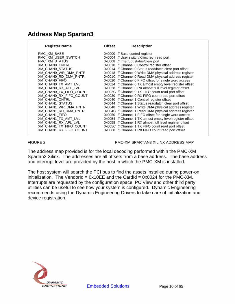
Address Map Spartan3
Register Name Offset Description
PMC_XM_BASE 0x0000 // Base control register PMC_XM_USER_SWITCH 0x0004 // User switch/Xilinx rev. read port PMC_XM_STATUS 0x0008 // Interrupt status/clear port XM_CHAN0_CNTRL 0x0010 // Channel 0 Control register offset XM_CHAN0_STATUS 0x0014 // Channel 0 Status read/latch clear port offset XM_CHAN0_WR_DMA_PNTR 0x0018 // Channel 0 Write DMA physical address register XM_CHAN0_RD_DMA_PNTR 0x001C // Channel 0 Read DMA physical address register XM_CHAN0_FIFO 0x0020 // Channel 0 FIFO offset for single word access XM_CHAN0_TX_AMT_LVL 0x0024 // Channel 0 TX almost empty level register offset XM_CHAN0_RX_AFL_LVL 0x0028 // Channel 0 RX almost full level register offset XM_CHAN0_TX_FIFO_COUNT 0x002C // Channel 0 TX FIFO count read port offset XM_CHAN0_RX_FIFO_COUNT 0x0030 // Channel 0 RX FIFO count read port offset XM_CHAN1_CNTRL 0x0040 // Channel 1 Control register offset XM_CHAN1_STATUS 0x0044 // Channel 1 Status read/latch clear port offset XM_CHAN1_WR_DMA_PNTR 0x0048 // Channel 1 Write DMA physical address register XM_CHAN1_RD_DMA_PNTR 0x004C // Channel 1 Read DMA physical address register XM_CHAN1_FIFO 0x0050 // Channel 1 FIFO offset for single word access XM_CHAN1_TX_AMT_LVL 0x0054 // Channel 1 TX almost empty level register offset XM_CHAN1_RX_AFL_LVL 0x0058 // Channel 1 RX almost full level register offset XM_CHAN1_TX_FIFO_COUNT 0x005C // Channel 1 TX FIFO count read port offset XM_CHAN1_RX_FIFO_COUNT 0x0060 // Channel 1 RX FIFO count read port offset
FIGURE 2 PMC-XM SPARTAN3 XILINX ADDRESS MAP
The address map provided is for the local decoding performed within the PMC-XM Spartan3 Xilinx. The addresses are all offsets from a base address. The base address and interrupt level are provided by the host in which the PMC-XM is installed. The host system will search the PCI bus to find the assets installed during power-on initialization. The VendorId = 0x10EE and the CardId = 0x0024 for the PMC-XM. Interrupts are requested by the configuration space. PCIView and other third party utilities can be useful to see how your system is configured. Dynamic Engineering recommends using the Dynamic Engineering Drivers to take care of initialization and device registration.
Embedded Solutions Page 11 of 65
Register Definitions
PMC_XM_BASE
[0x0000] Base Control Register (read/write)
Base Control Register
Data Bit Description 31-17 Spare 16 Load Virtex 15-10 Spare 9 Virtex Init 8 Virtex Reset 7 Virtex Flash Enable 6 Slave Serial Mode Enable 5 Virtex Program Init 4 Virtex Program Select 3 Flash Select 2 Flash Control 1 Force Interrupt 0 Master Interrupt Enable
FIGURE 3 PMC-XM SPARTAN3 BASE CONTROL REGISTER
All bits are active high and default to ‘0’ on reset or power-up. Master Interrupt Enable: This bit enables the interrupts for the base portion of the XM design. When this bit is a ‘1’, the interrupt is enabled; and when this bit is a ‘0’ the interrupt is disabled. Currently the only interrupt source for this portion of the design is the Force Interrupt bit. Force Interrupt: When this bit is ‘1’ and the Master Interrupt Enable is ‘1’, an interrupt will be generated. This bit is useful for software development and debugging. Flash Control: When this bit is ‘1’, the Flash Select bit controls which Flash Prom is connected to the JTAG port. When this bit is ‘0’, I/O bit 63 controls the selection. When I/O bit 63 is grounded, the Virtex Flash is selected; when I/O bit 63 is open, the signal is pulled high and the Spartan3 Flash is selected. Flash Select: When Flash Control is set to ‘1’ this bit controls which Flash Prom is connected to the JTAG port. When Flash Select is ‘0’, the Virtex Flash is selected; when Flash Select is ‘1’, the Spartan3 Flash is selected. When Flash Control is ‘0’, this bit has no effect.

Embedded Solutions Page 12 of 65
Virtex Program Select: When this bit is ‘1’, the Virtex Flash is controlled by the Virtex Flash Enable bit. When this bit is ‘0’, the Virtex Flash is controlled by the Virtex done bit. Virtex Program Init: When this bit is set to ‘1’ it forces the Virtex to re-configure from the Flash Prom. When this bit is ‘0’, the Virtex can be re-configured by a bit-file load. Slave Serial Mode Enable: When this bit is set to ‘1’, slave serial programming mode is selected on the Virtex. When this bit is ‘0’ master serial mode is selected. Slave serial mode is used when the Virtex is programmed from a file by the Spartan3 and master serial mode is used when the Virtex configures from the on-board flash. Virtex Flash Enable: When this bit is ‘0’ and the Virtex Program Select bit is ‘1’, the Virtex flash is disabled so that the Spartan3 can program the Virtex from a bit-file. Virtex Reset: When this bit is ‘1’, all the registers and FIFOs in the Virtex are reset. When this bit is ‘0’, the Virtex can resume normal operation. Virtex Init: When set to ‘1’, this bit delays configuration when a configuration cycle has been initiated. When this bit transitions to ‘0’, the mode bits are sampled and the configuration can proceed. The bit then becomes a status bit, which is read from the Status register, a ‘0’ indicating a CRC error. Load Virtex: when set to ‘1’, begins the process of programming the Virtex device from a bit-file. The data must be read from the file and loaded into the TX0 FIFO. When the hardware detects that the load is complete this bit will be automatically cleared.
Embedded Solutions Page 13 of 65
PMC_XM_USER_SWITCH
[0x0004] User Switch Port (read only)
Dip-Switch Port
Data Bit Description 31-16 Spare 15-8 Xilinx Design Revision Number 7-0 Sw7-0
FIGURE 4 PMC-XM SPARTAN3 USER SWITCH PORT
Sw7-0: The user switch is read through this read-only port. The bits are read as the lowest byte. Access the port as a long word and mask off the undefined bits. The dip-switch positions are defined in the silkscreen. For example the switch figure below indicates a 0x12.
Xilinx design revision number: The value of the second byte of this port is the rev. number of the Xilinx design (currently 0x05 - rev. E).
1
7 0
0
Embedded Solutions Page 14 of 65
PMC_XM_STATUS [0x0008] Status Register Read / Latch Clear Write
Status Register
Data Bit Description 31 Interrupt Status 30-24 Spare 23 Virtex Status 3 22 Virtex Status 2 21 Virtex Status 1 20 Virtex Status 0 19-10 Spare 9 Virtex Init Status 8 Virtex Configuration Done 7-1 Spare 0 Local Interrupt Active
FIGURE 5 PMC-XM SPARTAN3 STATUS REGISTER
Local Interrupt Active: When read as a ‘1’, a local interrupt condition is active. Currently, the only such condition is the Force Interrupt bit in the Base Control Register. A system interrupt will not occur unless the Master Interrupt Enable bit in the Base Control Register is also set. When read as a ‘0’, no local interrupt conditions are active. Virtex Configuration Done: When read as a ‘1’, the Virtex FPGA has successfully configured. When read as a ‘0’, the Virtex configuration was not successful. Virtex Init Status: When read as a ‘1’ after the Virtex configuration, it indicates that a CRC error did not occur during the Virtex configuration. When read as a ‘0’ after the Virtex configuration, it indicates that a CRC error occurred during the previous Virtex configuration. In this case the Done bit should also be low. Virtex Status 3-0: These bits are driven by the Virtex to indicate arbitrary status conditions. In the current Virtex ATP design they are all low, but they can be assigned for any purpose desired. Interrupt Status: When read as a ‘1’, an enabled local interrupt condition is active and a system interrupt should be asserted. When read as a ‘0’, no enabled local interrupt is active.
Embedded Solutions Page 15 of 65
XM_CHAN0/1_CNTRL
[0x0010, 0x0040] Channel Control Register (read/write]
Control Register
Data Bit Description 31-9 Spare 11 DMA Read Arbitration Priority Enable 10 DMA Write Arbitration Priority Enable 9 Virtex Interrupt Enable 8 Receive Enable 7 Transmit Enable 6 Force Interrupt 5 Master Interrupt Enable 4 DMA Read Enable 3 DMA Write Enable 2 FIFO Bypass 1 RX FIFO Reset 0 TX FIFO Reset
FIGURE 6 PMC-XM SPARTAN3 CHANNEL CONTROL REGISTER
TX/RX FIFO Reset: When this bit is ‘1’, the transmit or receive FIFO for the referenced channel is placed in a reset condition. When this bit is ‘0’, the corresponding FIFO is in a normal operational state. FIFO Bypass: When this bit is ‘1’, any data written to the transmit FIFO will be transferred to the receive FIFO as long as there is room in the receive FIFO. This facilitates FIFO loop-back testing. When this bit is ‘0’, data written to the transmit FIFO will remain in the FIFO until read by the data transfer state machine. DMA Write Enable: When this bit is ‘1’, the write DMA interrupt is enabled for the referenced channel. When this bit is ‘0’, the write DMA interrupt is disabled. DMA Read Enable: When this bit is ‘1’, the read DMA interrupt is enabled for the referenced channel. When this bit is ‘0’, the read DMA interrupt is disabled. Master Interrupt Enable: This bit enables the local interrupts for the referenced channel. When this bit is a ‘1’, the interrupt is enabled; and when this bit is a ‘0’ the interrupt is disabled. Currently the only interrupt source for this portion of the design is the Force Interrupt bit in this register. Force Interrupt: When this bit is ‘1’ and the Master Enable is a ‘1’, a system interrupt will occur. This bit is useful for software development and debugging.

Embedded Solutions Page 16 of 65
Transmit Enable: When this bit is ‘1’, the transfer state machine is enabled to move data from the referenced channel’s transmit FIFO to the corresponding Virtex transmit FIFO. When this bit is ‘0’, the transmit transfer state machine is disabled. Receive Enable: When this bit is ‘1’, the transfer state machine is enabled to move data from the referenced channel’s Virtex receive FIFO to the corresponding local receive FIFO. When this bit is ‘0’, the receive transfer state machine is disabled. Virtex Interrupt Enable: When this bit is ‘1’, the corresponding Virtex interrupt (VINT0 for channel 0 or VINT1 for channel 1) is enabled to cause a system interrupt when active. When this bit is ‘0’, the Virtex interrupt cannot cause a system interrupt. DMA Write Arbitration Priority Enable: When this bit is ‘1’, the write DMA for the referenced channel will receive priority if the TX FIFO has become almost empty as defined by the value stored in the TX_AMT_LVL register. When this bit is ‘0’, the DMA arbitration will follow round-robin arbitration priority. DMA Read Arbitration Priority Enable: When this bit is ‘1’, the read DMA for the referenced channel will receive priority if the RX FIFO has become almost full as defined by the value stored in the RX_AFL_LVL register. When this bit is ‘0’, the DMA arbitration will follow round-robin arbitration priority.
Embedded Solutions Page 17 of 65
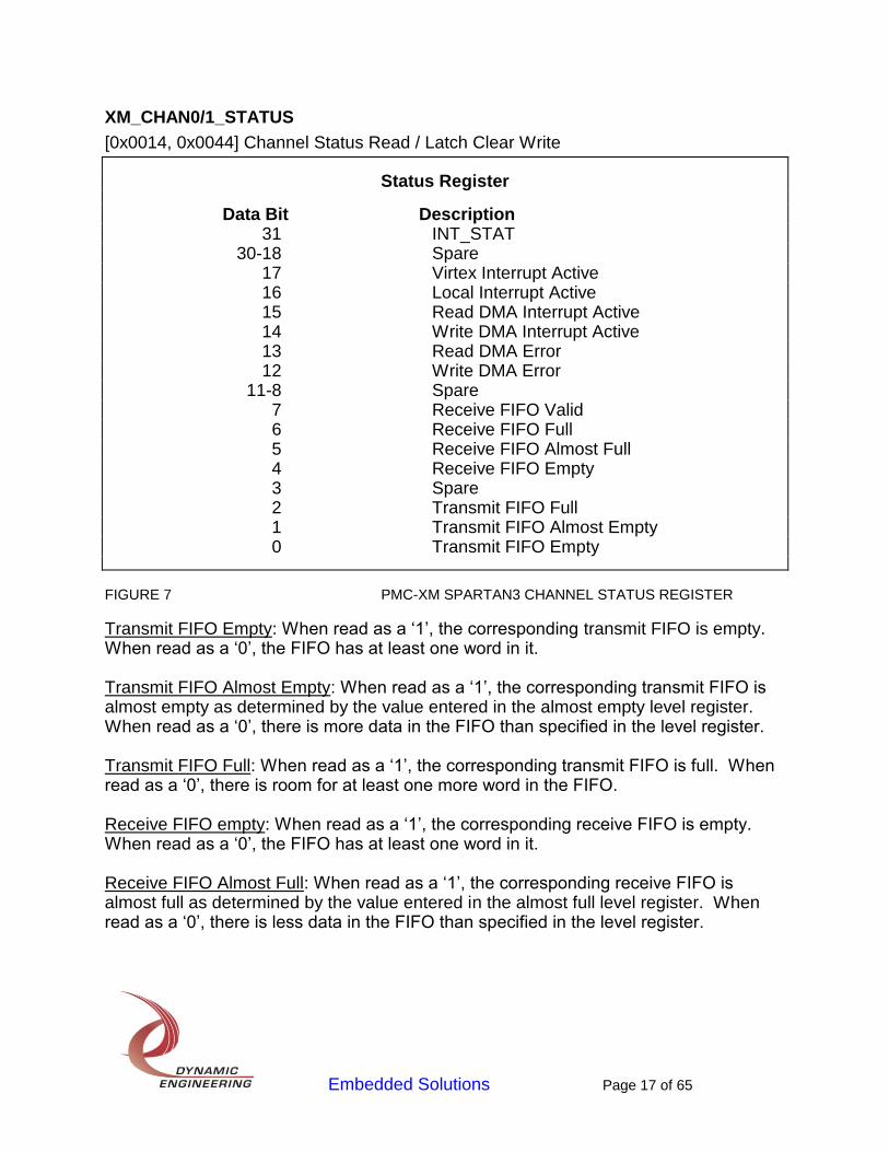
XM_CHAN0/1_STATUS
[0x0014, 0x0044] Channel Status Read / Latch Clear Write
Status Register
Data Bit Description 31 INT_STAT 30-18 Spare 17 Virtex Interrupt Active 16 Local Interrupt Active 15 Read DMA Interrupt Active 14 Write DMA Interrupt Active 13 Read DMA Error 12 Write DMA Error 11-8 Spare 7 Receive FIFO Valid 6 Receive FIFO Full 5 Receive FIFO Almost Full 4 Receive FIFO Empty 3 Spare 2 Transmit FIFO Full 1 Transmit FIFO Almost Empty 0 Transmit FIFO Empty
FIGURE 7 PMC-XM SPARTAN3 CHANNEL STATUS REGISTER
Transmit FIFO Empty: When read as a ‘1’, the corresponding transmit FIFO is empty. When read as a ‘0’, the FIFO has at least one word in it. Transmit FIFO Almost Empty: When read as a ‘1’, the corresponding transmit FIFO is almost empty as determined by the value entered in the almost empty level register. When read as a ‘0’, there is more data in the FIFO than specified in the level register. Transmit FIFO Full: When read as a ‘1’, the corresponding transmit FIFO is full. When read as a ‘0’, there is room for at least one more word in the FIFO. Receive FIFO empty: When read as a ‘1’, the corresponding receive FIFO is empty. When read as a ‘0’, the FIFO has at least one word in it. Receive FIFO Almost Full: When read as a ‘1’, the corresponding receive FIFO is almost full as determined by the value entered in the almost full level register. When read as a ‘0’, there is less data in the FIFO than specified in the level register.
Embedded Solutions Page 18 of 65
Receive FIFO Full: When read as a ‘1’, the corresponding receive FIFO is full. When read as a ‘0’, there is room for at least one more word in the FIFO. Receive FIFO Valid: When read as a ‘1’, there is valid receive data to read. When read as a ‘0’, there is no valid receive data. There is a four-deep pipeline on the output of the RX FIFO that will be filled before data is retained in the FIFO. Therefore even though the FIFO is empty there may actually be up to four long-words of valid receive data. This status bit indicates when there is valid data even though the FIFO is empty. Write DMA Error: When read as a ‘1’, a write DMA error has been detected. This will occur if there is a target or master abort or if the direction bit in the next pointer of one of the chaining descriptors is a one. When read as a ‘0’, no error has occurred. Read DMA Error: When read as a ‘1’, a read DMA error has been detected. This will occur if there is a target or master abort or if the direction bit in the next pointer of one of the chaining descriptors is a zero. When read as a ‘0’, no error has occurred. Write DMA Interrupt Active: When read as a ‘1’, a write DMA interrupt is latched. This indicates that the scatter-gather list for the current write DMA has completed, but the associated interrupt has yet to be completely processed. When read as a ‘0’, no write DMA interrupt is pending. Read DMA Interrupt Active: When read as a ‘1’, a read DMA interrupt is latched. This indicates that the scatter-gather list for the current read DMA has completed, but the associated interrupt has yet to be completely processed. When read as a ‘0’, no read DMA interrupt is pending Local Interrupt Active: When read as a ‘1’, a local interrupt condition is active for the referenced channel. Currently, the only such condition is the Force Interrupt bit in the Channel Control Register. A system interrupt will not occur unless the Master Interrupt Enable bit in the Channel Control Register is also set. When read as a ‘0’, no local interrupt conditions are active. Virtex Interrupt Active: When read as a ‘1’, the corresponding Virtex interrupt (VINT0 for channel 0 or VINT1 for channel 1) is active. A system interrupt will not occur unless the Virtex Interrupt Enable in the Channel Control Register is set. When read as a ‘0’, the Virtex interrupt is inactive. INT_STAT: When read as a ‘1’, an enabled channel interrupt condition is active and a system interrupt should be asserted. When read as a ‘0’, no enabled channel interrupt is active.
Embedded Solutions Page 19 of 65
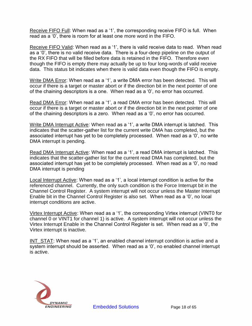
XM_CHAN0/1_WR/RD_DMA_PNTR
[0x0018, 0x001C, 0x0048, 0x004C] DMA Address Register (Write only)
DMA Pointer Address Register
Data Bit Description 31-0 First Chaining Descriptor Physical Address
FIGURE 8 PMC-XM SPARTAN3 CHANNEL DMA POINTER REGISTER
These write-only ports are used to initiate scatter-gather DMAs. When the physical address of the first chaining descriptor is written to one of these ports, the corresponding DMA engine reads three successive long words beginning at that address. The first is the address of the first memory block of the DMA buffer, the second is the length in bytes of that block, and the third is the address of the next chaining descriptor in the list of buffer memory blocks. This process is continued until a bit in one of the next pointer values read indicates that it is the end of the chain. Note: Writing a zero to one of these ports will abort the associated DMA if one is in progress.
XM_CHAN0/1_FIFO
[0x0020, 0x0050] Write TX/Read RX FIFO Port
TX / RX FIFO Port
Data Bit Description 31-0 FIFO Data 31-0
FIGURE 9 PMC-XM SPARTAN3 CHANNEL FIFO PORT
Data written to this address is written into the transmit FIFO as long as the FIFO is not full. When this address is read a data-word is read from the receive FIFO. When the receive FIFO becomes empty, the last data-word that was in the FIFO will be returned.
Embedded Solutions Page 20 of 65
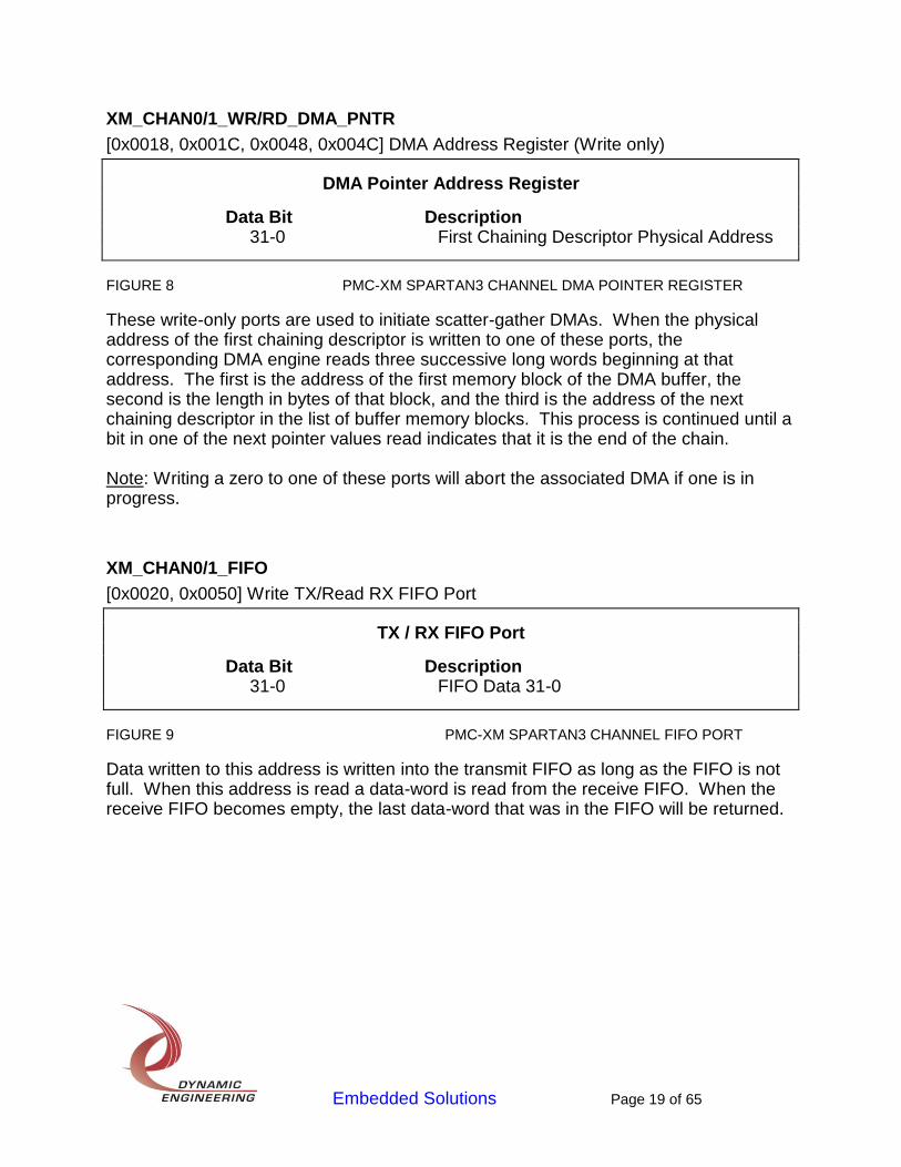
XM_CHAN0/1_TX_AMT_LVL
[0x0024, 0x0054] TX Almost Empty Level Register (read/write)
TX Almost Empty Level Register
Data Bit Description 31-16 Spare 15-0 TX FIFO Almost Empty Level
FIGURE 10 PMC-XM SPARTAN3 CHANNEL TX ALMOST EMPTY REGISTER
This register specifies the level at which the transmit FIFO almost empty level will be asserted. When the number of data words in the transmit FIFO is less than or equal to this count the almost empty status will be asserted.
XM_CHAN0/1_RX_AFL_LVL
[0x0028, 0x0058] RX Almost Full Level Register (read/write)
RX Almost Full Level Register
Data Bit Description 31-16 Spare 15-0 RX FIFO Almost Full Level
FIGURE 11 PMC-XM SPARTAN3 CHANNEL RX ALMOST FULL REGISTER
This register specifies the level at which the receive FIFO almost full level will be asserted. When the number of data words in the receive FIFO is greater than or equal to this count the almost full status will be asserted.
Embedded Solutions Page 21 of 65
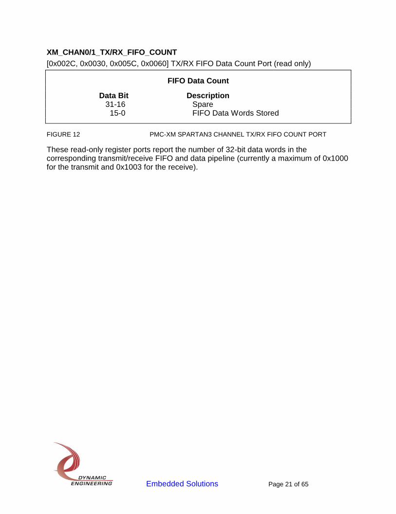
XM_CHAN0/1_TX/RX_FIFO_COUNT
[0x002C, 0x0030, 0x005C, 0x0060] TX/RX FIFO Data Count Port (read only)
FIFO Data Count
Data Bit Description 31-16 Spare 15-0 FIFO Data Words Stored
FIGURE 12 PMC-XM SPARTAN3 CHANNEL TX/RX FIFO COUNT PORT
These read-only register ports report the number of 32-bit data words in the corresponding transmit/receive FIFO and data pipeline (currently a maximum of 0x1000 for the transmit and 0x1003 for the receive).
Embedded Solutions Page 22 of 65
EADIN/Modbus Virtex Design Product Description
The EADIN/Modbus Virtex design implements 32 independent communication channels. Each channel communicates over a single RS485 differential I/O line at 1 M bit/second using differential Manchester encoding. This design does not use DMA. All message data accesses are made directly to the target channel's FIFOs. The interrupts for all 32 channels are connected to VINT0, the interrupt associated with Spartan channel 0. A read only register at the Virtex base level returns a 32-bit mask of the channels with active interrupts. Any channel can be configured to operate as a bus-master, addressable slave node or bus-monitor. Channels 0 – 5 and 8 – 31 use the Engine Area Distributed Interconnect Network bus protocol, while channels 6 and 7 use the Modbus protocol. Each channel has two 1K by 32-bit FIFOs, one for the transmit function and one for the receive function. The transmit FIFO is written from the PCI bus and stores commands, addresses, counts, and data that will be sent out on its I/O bus. The receive FIFO is read from the PCI bus and stores commands, addresses, counts, data and CRC values that are received from other connected bus-nodes on the same I/O bus. An onboard PLL supplies two clocks for circuit operation. Clock A is set to 8 MHz and is used to encode and decode the 1 Mbps differential Manchester I/O signals as well as other I/O circuit functions. Clock B is set to 400 KHz and is used to generate the start pulses that are used by the bus-master to trigger timed message transmission with an interval of one or two milliseconds. Each channel has a CRC calculator that generates a 16-bit CRC code that is appended to each frame by the transmitting node. The receiving node calculates a CRC code on the data it receives and compares this to the CRC that it receives over the bus. The bus-master appends the CRC for the initial command request and the target slave calculates and verifies this CRC. For commands that require a response, the target slave node appends the CRC to the response data, and the bus-master calculates and verifies this CRC. Two different programmable CRC polynomials are stored at the base level that can be selected independently by each channel.
Embedded Solutions Page 23 of 65
EADIN/Modbus Virtex Design Theory of Operation
When operating in the system, a bus-master node sends one message either every millisecond or every two milliseconds. Two pulses are created at the base level to trigger the sending of these messages. These pulses each have a two millisecond period, but are offset by one millisecond from each other. A bus-master channel can be configured to respond to any combination of these pulses. When the bus-master channel is configured to use the start pulse(s), it will send one message in response to each pulse. If the channel doesn’t use any start pulses, it sends messages as long as its start bit is set and message data is present in the FIFO. If transmit start clear is enabled, the start bit will be cleared at the end of each message. Each channel has a selectable parallel effective I/O termination of 100 ohms. If selected, this termination is active only when the channel is operating as a receiver. If multiple slave or bus-monitor nodes are present on the same I/O bus, care should be taken to ensure that the bus is not loaded with multiple terminations as this will degrade the signal amplitude. A bus-monitor node will always operate as a receiver and will store all byte-data on the bus in the order that it is seen. The data is stored in a 32-bit word starting with the least significant byte. When all four bytes in a word have been filled, the word is written to the channel's receive FIFO. When the channel is disabled, any partially filled word will be written with the unused bytes filled with zeros.
EADIN Protocol
The Engine Area Distributed Interconnect Network (EADIN) based on the Local Interconnect Network (LIN) is a master/slave identifier-based serial protocol. All communication is initiated by the bus-master. The target of each message is one of up to 16 slave nodes, specified by the low four bits (0-3) in the protected identifier field (PID). The upper two bits in the PID are parity bits defined by the following equations. eq.1 Bit 6 = ID0 xor ID1 xor ID2 xor ID4 eq.2 Bit 7 = not (ID1 xor ID3 xor ID4 xor ID5) When enabled and no frame is active, the bus-master continuously drives the I/O bus with a differential Manchester '1' value. Each frame begins with a break field consisting of 13 bits of zero followed by a single bit of one. All other fields are 10 bits consisting of a low start bit, 8 data bits and a high stop bit. The break is followed by a sync byte of 0x55, PID, address, length and CRC. For this design, only bulk unicast writes and reads are implemented. These commands require a second user-defined frame with a PID of 62 decimal (0x3e). Adding the two parity bits yields the 8-bit value 0xfe. Immediately following the 62 PID, the data-bytes are transferred. The transfer direction is from master to slave for a write and from slave
Embedded Solutions Page 24 of 65
to master for a read. All transfers involve the bus-master and a single slave node, there is no provision for broadcast write transfers.
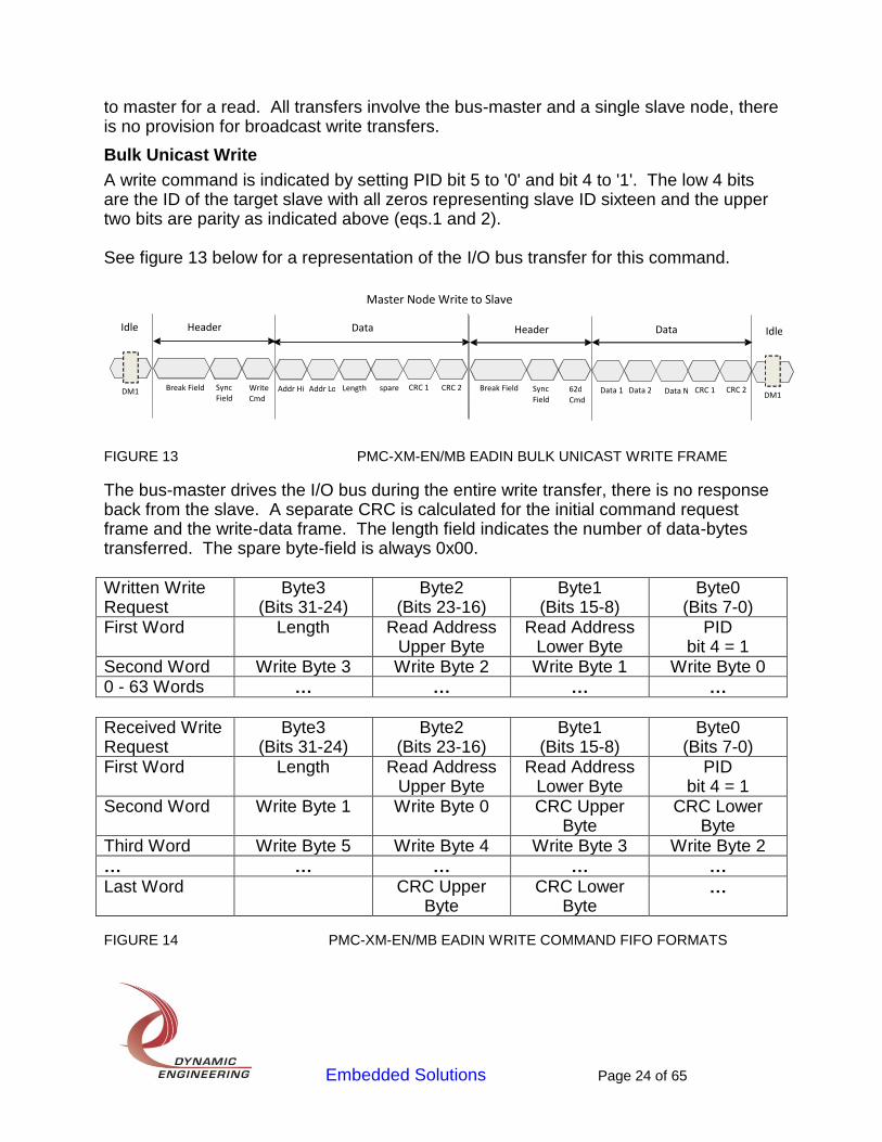
Bulk Unicast Write
A write command is indicated by setting PID bit 5 to '0' and bit 4 to '1'. The low 4 bits are the ID of the target slave with all zeros representing slave ID sixteen and the upper two bits are parity as indicated above (eqs.1 and 2). See figure 13 below for a representation of the I/O bus transfer for this command.
FIGURE 13 PMC-XM-EN/MB EADIN BULK UNICAST WRITE FRAME
The bus-master drives the I/O bus during the entire write transfer, there is no response back from the slave. A separate CRC is calculated for the initial command request frame and the write-data frame. The length field indicates the number of data-bytes transferred. The spare byte-field is always 0x00. Written Write Request
Byte3 (Bits 31-24)
Byte2 (Bits 23-16)
Byte1 (Bits 15-8)
Byte0 (Bits 7-0)
First Word Length Read Address Upper Byte
Read Address Lower Byte
PID bit 4 = 1
Second Word Write Byte 3 Write Byte 2 Write Byte 1 Write Byte 0 0 - 63 Words … … … … Received Write Request
Byte3 (Bits 31-24)
Byte2 (Bits 23-16)
Byte1 (Bits 15-8)
Byte0 (Bits 7-0)
First Word Length Read Address Upper Byte
Read Address Lower Byte
PID bit 4 = 1
Second Word Write Byte 1 Write Byte 0 CRC Upper Byte
CRC Lower Byte
Third Word Write Byte 5 Write Byte 4 Write Byte 3 Write Byte 2
… … … … … Last Word CRC Upper
Byte CRC Lower
Byte …
FIGURE 14 PMC-XM-EN/MB EADIN WRITE COMMAND FIFO FORMATS
Length
Master Node Write to Slave
Addr Hi Addr Lo CRC 1
Data
CRC 2 spare
Header
Break Field Sync Field
Write Cmd
Data 1 CRC 1 CRC 2 Data 2 Data N
Data Header
Break Field Sync Field
62d Cmd DM1 DM1
Idle Idle
Embedded Solutions Page 25 of 65
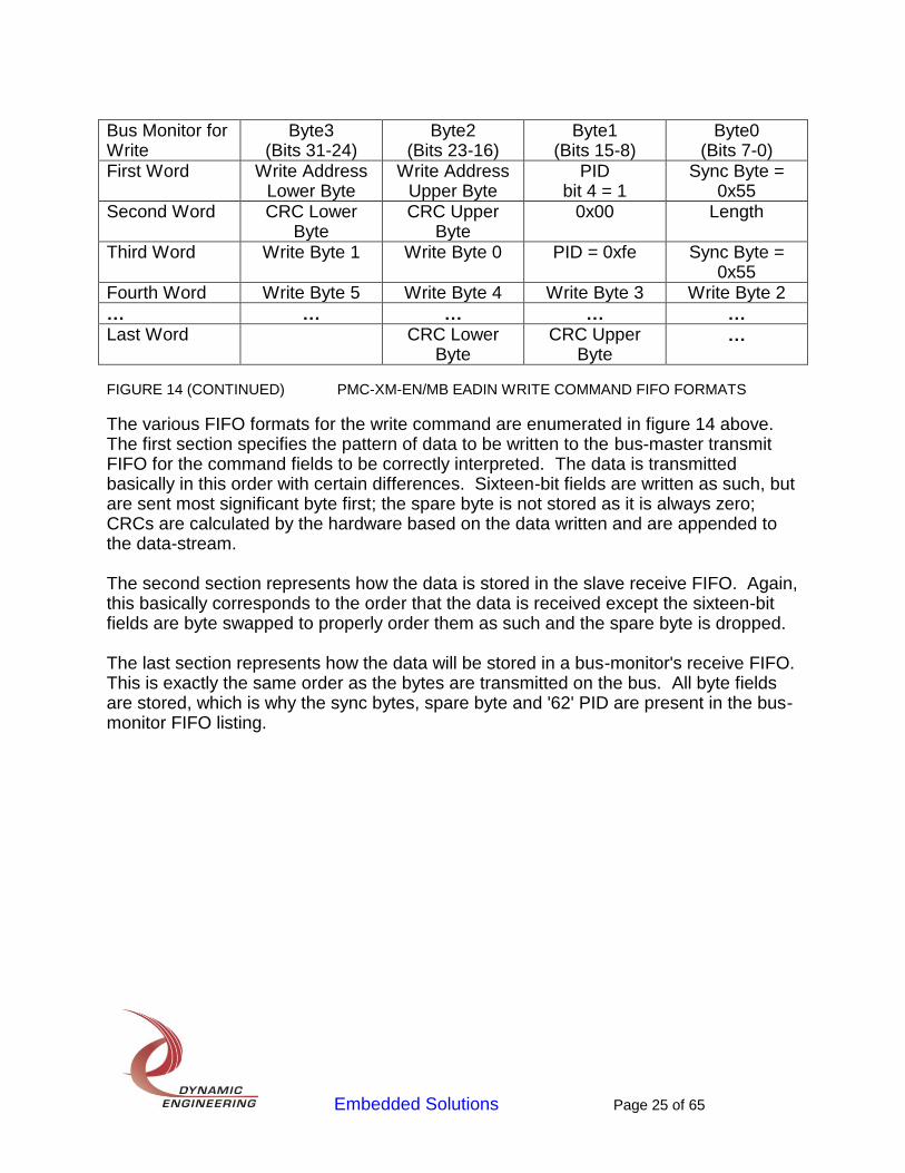
Bus Monitor for Write
Byte3 (Bits 31-24)
Byte2 (Bits 23-16)
Byte1 (Bits 15-8)
Byte0 (Bits 7-0)
First Word Write Address Lower Byte
Write Address Upper Byte
PID bit 4 = 1
Sync Byte = 0x55
Second Word CRC Lower Byte
CRC Upper Byte
0x00 Length
Third Word Write Byte 1 Write Byte 0 PID = 0xfe Sync Byte = 0x55
Fourth Word Write Byte 5 Write Byte 4 Write Byte 3 Write Byte 2
… … … … … Last Word CRC Lower
Byte CRC Upper
Byte …
FIGURE 14 (CONTINUED) PMC-XM-EN/MB EADIN WRITE COMMAND FIFO FORMATS
The various FIFO formats for the write command are enumerated in figure 14 above. The first section specifies the pattern of data to be written to the bus-master transmit FIFO for the command fields to be correctly interpreted. The data is transmitted basically in this order with certain differences. Sixteen-bit fields are written as such, but are sent most significant byte first; the spare byte is not stored as it is always zero; CRCs are calculated by the hardware based on the data written and are appended to the data-stream. The second section represents how the data is stored in the slave receive FIFO. Again, this basically corresponds to the order that the data is received except the sixteen-bit fields are byte swapped to properly order them as such and the spare byte is dropped. The last section represents how the data will be stored in a bus-monitor's receive FIFO. This is exactly the same order as the bytes are transmitted on the bus. All byte fields are stored, which is why the sync bytes, spare byte and '62' PID are present in the bus-monitor FIFO listing.
Embedded Solutions Page 26 of 65
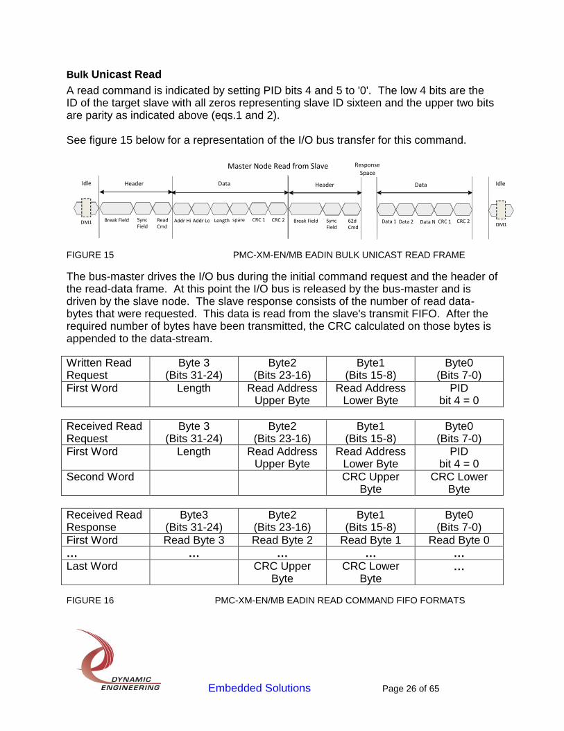
Bulk Unicast Read
A read command is indicated by setting PID bits 4 and 5 to '0'. The low 4 bits are the ID of the target slave with all zeros representing slave ID sixteen and the upper two bits are parity as indicated above (eqs.1 and 2). See figure 15 below for a representation of the I/O bus transfer for this command.
FIGURE 15 PMC-XM-EN/MB EADIN BULK UNICAST READ FRAME
The bus-master drives the I/O bus during the initial command request and the header of the read-data frame. At this point the I/O bus is released by the bus-master and is driven by the slave node. The slave response consists of the number of read data-bytes that were requested. This data is read from the slave's transmit FIFO. After the required number of bytes have been transmitted, the CRC calculated on those bytes is appended to the data-stream.
Written Read Request
Byte 3 (Bits 31-24)
Byte2 (Bits 23-16)
Byte1 (Bits 15-8)
Byte0 (Bits 7-0)
First Word Length Read Address Upper Byte
Read Address Lower Byte
PID bit 4 = 0
Received Read Request
Byte 3 (Bits 31-24)
Byte2 (Bits 23-16)
Byte1 (Bits 15-8)
Byte0 (Bits 7-0)
First Word Length Read Address Upper Byte
Read Address Lower Byte
PID bit 4 = 0
Second Word CRC Upper Byte
CRC Lower Byte
Received Read Response
Byte3 (Bits 31-24)
Byte2 (Bits 23-16)
Byte1 (Bits 15-8)
Byte0 (Bits 7-0)
First Word Read Byte 3 Read Byte 2 Read Byte 1 Read Byte 0
… … … … … Last Word CRC Upper
Byte CRC Lower
Byte …
FIGURE 16 PMC-XM-EN/MB EADIN READ COMMAND FIFO FORMATS
Length
Master Node Read from Slave
Addr Hi Addr Lo CRC 1
Data
CRC 2 spare
Header
B reak Field Sync Field
Read Cmd Data 1 CRC 1 CRC 2 Data 2 Data N
Data Header
B reak Field Sync Field
62d Cmd DM1 DM1
Idle Idle
Response Space
Embedded Solutions Page 27 of 65
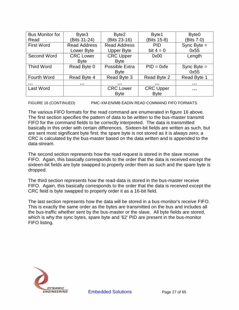
Bus Monitor for Read
Byte3 (Bits 31-24)
Byte2 (Bits 23-16)
Byte1 (Bits 15-8)
Byte0 (Bits 7-0)
First Word Read Address Lower Byte
Read Address Upper Byte
PID bit 4 = 0
Sync Byte = 0x55
Second Word CRC Lower Byte
CRC Upper Byte
0x00 Length
Third Word Read Byte 0 Possible Extra Byte
PID = 0xfe Sync Byte = 0x55
Fourth Word Read Byte 4 Read Byte 3 Read Byte 2 Read Byte 1
… … … … … Last Word CRC Lower
Byte CRC Upper
Byte …
FIGURE 16 (CONTINUED) PMC-XM-EN/MB EADIN READ COMMAND FIFO FORMATS
The various FIFO formats for the read command are enumerated in figure 16 above. The first section specifies the pattern of data to be written to the bus-master transmit FIFO for the command fields to be correctly interpreted. The data is transmitted basically in this order with certain differences. Sixteen-bit fields are written as such, but are sent most significant byte first; the spare byte is not stored as it is always zero; a CRC is calculated by the bus-master based on the data written and is appended to the data-stream. The second section represents how the read request is stored in the slave receive FIFO. Again, this basically corresponds to the order that the data is received except the sixteen-bit fields are byte swapped to properly order them as such and the spare byte is dropped. The third section represents how the read-data is stored in the bus-master receive FIFO. Again, this basically corresponds to the order that the data is received except the CRC field is byte swapped to properly order it as a 16-bit field. The last section represents how the data will be stored in a bus-monitor's receive FIFO. This is exactly the same order as the bytes are transmitted on the bus and includes all the bus-traffic whether sent by the bus-master or the slave. All byte fields are stored, which is why the sync bytes, spare byte and '62' PID are present in the bus-monitor FIFO listing.
Embedded Solutions Page 28 of 65
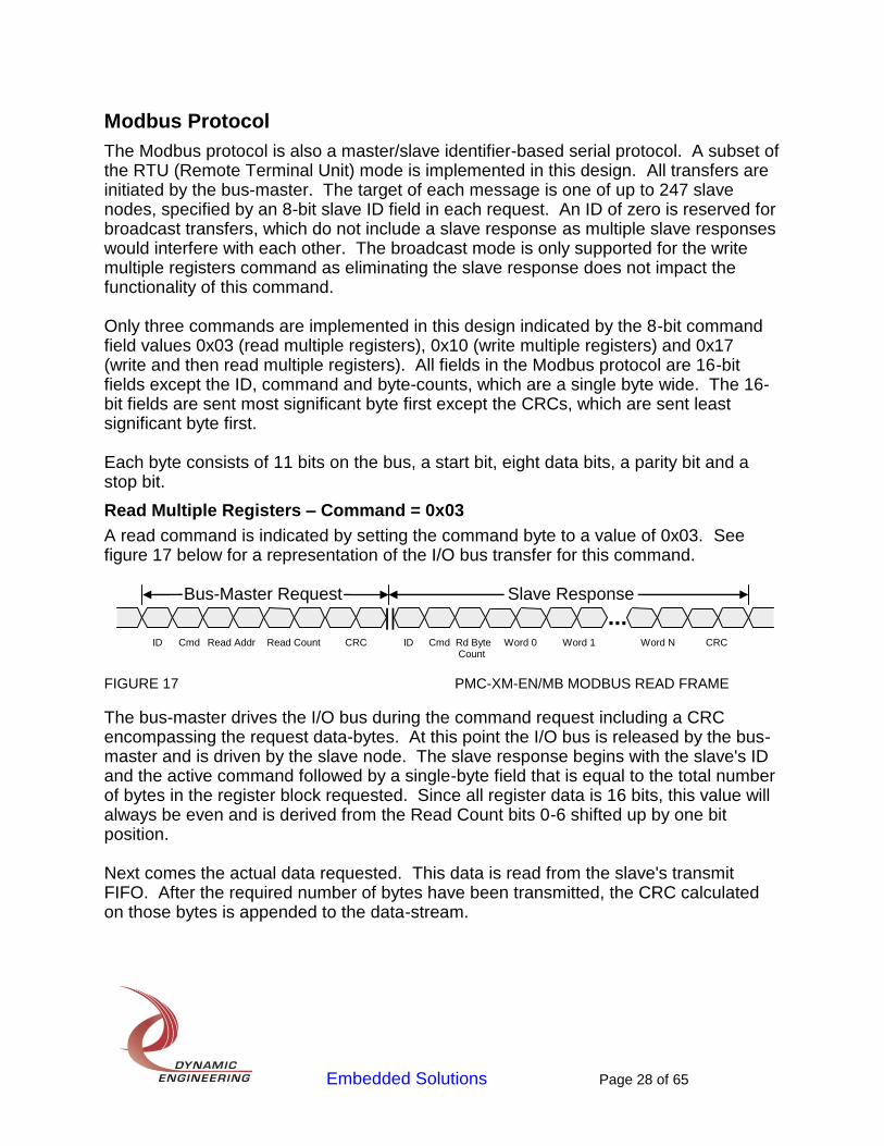
Modbus Protocol
The Modbus protocol is also a master/slave identifier-based serial protocol. A subset of the RTU (Remote Terminal Unit) mode is implemented in this design. All transfers are initiated by the bus-master. The target of each message is one of up to 247 slave nodes, specified by an 8-bit slave ID field in each request. An ID of zero is reserved for broadcast transfers, which do not include a slave response as multiple slave responses would interfere with each other. The broadcast mode is only supported for the write multiple registers command as eliminating the slave response does not impact the functionality of this command. Only three commands are implemented in this design indicated by the 8-bit command field values 0x03 (read multiple registers), 0x10 (write multiple registers) and 0x17 (write and then read multiple registers). All fields in the Modbus protocol are 16-bit fields except the ID, command and byte-counts, which are a single byte wide. The 16-bit fields are sent most significant byte first except the CRCs, which are sent least significant byte first. Each byte consists of 11 bits on the bus, a start bit, eight data bits, a parity bit and a stop bit.
Read Multiple Registers – Command = 0x03
A read command is indicated by setting the command byte to a value of 0x03. See figure 17 below for a representation of the I/O bus transfer for this command. Bus-Master Request Slave Response
|| ...
ID Cmd Read Addr Read Count CRC ID Cmd Rd Byte Word 0 Word 1 Word N CRC Count
FIGURE 17 PMC-XM-EN/MB MODBUS READ FRAME
The bus-master drives the I/O bus during the command request including a CRC encompassing the request data-bytes. At this point the I/O bus is released by the bus-master and is driven by the slave node. The slave response begins with the slave's ID and the active command followed by a single-byte field that is equal to the total number of bytes in the register block requested. Since all register data is 16 bits, this value will always be even and is derived from the Read Count bits 0-6 shifted up by one bit position. Next comes the actual data requested. This data is read from the slave's transmit FIFO. After the required number of bytes have been transmitted, the CRC calculated on those bytes is appended to the data-stream.

Embedded Solutions Page 29 of 65
Written Read Request
Byte3 (Bits 31-24)
Byte2 (Bits 23-16)
Byte1 (Bits 15-8)
Byte0 (Bits 7-0)
First Word Read Address Upper Byte
Read Address Lower Byte
Command = 0x03
Slave ID
Second Word Unused Unused Read Count Upper Byte
Read Count Lower Byte
Received Read Request
Byte3 (Bits 31-24)
Byte2 (Bits 23-16)
Byte1 (Bits 15-8)
Byte0 (Bits 7-0)
First Word 0x00 Command = 0x03
0x00 Slave ID
Second Word Read Count Upper Byte
Read Count Lower Byte
Read Address Upper Byte
Read Address Lower Byte
Third Word CRC Upper Byte
CRC Lower Byte
Received Read Response
Byte3 (Bits 31-24)
Byte2 (Bits 23-16)
Byte1 (Bits 15-8)
Byte0 (Bits 7-0)
First Word 0x00 Command = 0x03
0x00 Slave ID
Second Word Read Word 0 Upper Byte
Read Word 0 Lower Byte
0x00 Read Byte Count
… … … … … Last Word CRC Upper
Byte CRC Lower
Byte … …
Bus Monitor for Read
Byte3 (Bits 31-24)
Byte2 (Bits 23-16)
Byte1 (Bits 15-8)
Byte0 (Bits 7-0)
First Word Read Address Lower Byte
Read Address Upper Byte
Command = 0x03
Slave ID
Second Word CRC Upper Byte
CRC Lower Byte
Read Count Lower Byte
Read Count Upper Byte
Third Word Read Byte Count
Command = 0x03
Slave ID Possible Extra Byte
Fourth Word Read Word 1 Lower Byte
Read Word 1 Upper Byte
Read Word 0 Lower Byte
Read Word 0 Upper Byte
… … … … … Last Word CRC Upper
Byte CRC Lower
Byte … …
FIGURE 18 PMC-XM-EN/MB MODBUS READ COMMAND FIFO FORMATS
The various FIFO formats for the read command are enumerated in figure 18 above. The first section specifies the pattern of data to be written to the bus-master transmit
Embedded Solutions Page 30 of 65
FIFO for the command fields to be correctly interpreted. The data is transmitted basically in this order with certain differences. Sixteen-bit fields are written as such, but are sent most significant byte first except for the CRC, which is calculated by the bus-master based on the data written and is appended to the data-stream. The second section represents how the read request is stored in the slave receive FIFO. Again, this basically corresponds to the order that the data is received except sixteen-bit fields, other than the CRC, are byte swapped to properly order them as such and single-byte fields are expanded to 16 bits in order to preserve word alignment for the 16-bit register data. In the Modbus protocol CRCs are sent least significant byte first so there is no need for them to be byte swapped. The third section represents how the read response and data are stored in the bus-master receive FIFO. Again, this basically corresponds to the order that the data is received except sixteen-bit fields, other than the CRC, are byte swapped to properly order them as such and single-byte fields are expanded to 16 bits in order to preserve word alignment for the 16-bit register data. The last section represents how the data will be stored in a bus-monitor's receive FIFO. This is exactly the same order as the bytes are transmitted on the bus and includes all the bus-traffic whether sent by the bus-master or a slave.
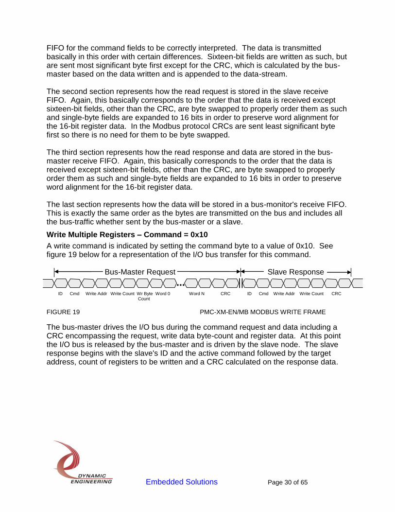
Write Multiple Registers – Command = 0x10
A write command is indicated by setting the command byte to a value of 0x10. See figure 19 below for a representation of the I/O bus transfer for this command. Bus-Master Request Slave Response
... ||
ID Cmd Write Addr Write Count Wr Byte Word 0 Word N CRC ID Cmd Write Addr Write Count CRC Count
FIGURE 19 PMC-XM-EN/MB MODBUS WRITE FRAME
The bus-master drives the I/O bus during the command request and data including a CRC encompassing the request, write data byte-count and register data. At this point the I/O bus is released by the bus-master and is driven by the slave node. The slave response begins with the slave's ID and the active command followed by the target address, count of registers to be written and a CRC calculated on the response data.
Embedded Solutions Page 31 of 65
Written Write Request
Byte3 (Bits 31-24)
Byte2 (Bits 23-16)
Byte1 (Bits 15-8)
Byte0 (Bits 7-0)
First Word Write Address Upper Byte
Write Address Lower Byte
Command = 0x10
Slave ID
Second Word Write Word 0 Upper Byte
Write Word 0 Lower Byte
Write Count Upper Byte
Write Count Lower Byte
Third Word Write Word 2 Upper Byte
Write Word 2 Lower Byte
Write Word 1 Upper Byte
Write Word 1 Lower Byte
… … … … … Received Write Request
Byte3 (Bits 31-24)
Byte2 (Bits 23-16)
Byte1 (Bits 15-8)
Byte0 (Bits 7-0)
First Word 0x00 Command = 0x10
0x00 Slave ID
Second Word Write Count Upper Byte
Write Count Lower Byte
Write Address Upper Byte
Write Address Lower Byte
Third Word Write Word 0 Upper Byte
Write Word 0 Lower Byte
0x00 Write Byte Count
Fourth Word Write Word 2 Upper Byte
Write Word 2 Lower Byte
Write Word 1 Upper Byte
Write Word 1 Lower Byte
… … … … … CRC Upper
Byte CRC Lower
Byte Received Write Response
Byte3 (Bits 31-24)
Byte2 (Bits 23-16)
Byte1 (Bits 15-8)
Byte0 (Bits 7-0)
First Word 0x00 Command = 0x10
0x00 Slave ID
Second Word Write Count Upper Byte
Write Count Lower Byte
Write Address Upper Byte
Write Address Lower Byte
Third Word CRC Upper Byte
CRC Lower Byte
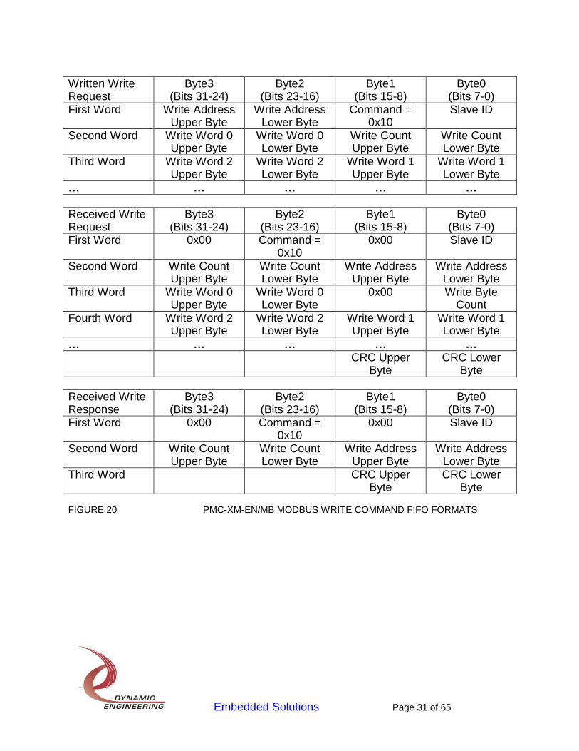
FIGURE 20 PMC-XM-EN/MB MODBUS WRITE COMMAND FIFO FORMATS
Embedded Solutions Page 32 of 65
Bus Monitor for Write
Byte3 (Bits 31-24)
Byte2 (Bits 23-16)
Byte1 (Bits 15-8)
Byte0 (Bits 7-0)
First Word Write Address Lower Byte
Write Address Upper Byte
Command = 0x10
Slave ID
Second Word Write Word 0 Upper Byte
Write Byte Count
Write Count Lower Byte
Write Count Upper Byte
Third Word Write Word 2 Upper Byte
Write Word 1 Lower Byte
Write Word 1 Upper Byte
Write Word 0 Lower Byte
… … … … … Last – 2 Word Possible Extra
Byte CRC Upper
Byte CRC Lower
Byte …
Last – 1 Word Write Address Lower Byte
Write Address Upper Byte
Command = 0x10
Slave ID
Last Word CRC Upper Byte
CRC Lower Byte
Write Count Lower Byte
Write Count Upper Byte
FIGURE 20 (CONTINUED) PMC-XM-EN/MB MODBUS WRITE COMMAND FIFO FORMATS
The various FIFO formats for the write command are enumerated in figure 20 above. The first section specifies the pattern of data to be written to the bus-master transmit FIFO for the command fields to be correctly interpreted. The data is transmitted basically in this order with certain differences. Sixteen-bit fields are written as such, but are sent most significant byte first except for the CRC, which is calculated by the bus-master based on the data written and is appended to the data-stream. The second section represents how the write request and data are stored in the slave receive FIFO. Again, this basically corresponds to the order that the data is received except sixteen-bit fields, other than the CRC, are byte swapped to properly order them as such and single-byte fields are expanded to 16 bits in order to preserve word alignment for the 16-bit register data. In the Modbus protocol CRCs are sent least significant byte first so there is no need for them to be byte swapped. The third section represents how the write response is stored in the bus-master receive FIFO. Again, this basically corresponds to the order that the data is received except sixteen-bit fields, other than the CRC, are byte swapped to properly order them as such and single-byte fields are expanded to 16 bits in order to preserve word alignment for the 16-bit register data. The last section represents how the data will be stored in a bus-monitor's receive FIFO. This is exactly the same order as the bytes are transmitted on the bus and includes all the bus-traffic whether sent by the bus-master or a slave. For a broadcast write command, the slave ID will be zero and there will be no slave response.
Embedded Solutions Page 33 of 65
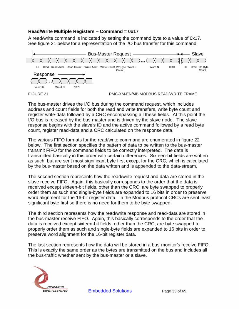
Read/Write Multiple Registers – Command = 0x17
A read/write command is indicated by setting the command byte to a value of 0x17. See figure 21 below for a representation of the I/O bus transfer for this command. Bus-Master Request Slave
... ||
ID Cmd Read Addr Read Count Write Addr Write Count Wr Byte Word 0 Word N CRC ID Cmd Rd Byte Count Count
Response
...
Word 0 Word N CRC
FIGURE 21 PMC-XM-EN/MB MODBUS READ/WRITE FRAME
The bus-master drives the I/O bus during the command request, which includes address and count fields for both the read and write transfers, write byte count and register write-data followed by a CRC encompassing all these fields. At this point the I/O bus is released by the bus-master and is driven by the slave node. The slave response begins with the slave's ID and the active command followed by a read byte count, register read-data and a CRC calculated on the response data.
The various FIFO formats for the read/write command are enumerated in figure 22 below. The first section specifies the pattern of data to be written to the bus-master transmit FIFO for the command fields to be correctly interpreted. The data is transmitted basically in this order with certain differences. Sixteen-bit fields are written as such, but are sent most significant byte first except for the CRC, which is calculated by the bus-master based on the data written and is appended to the data-stream. The second section represents how the read/write request and data are stored in the slave receive FIFO. Again, this basically corresponds to the order that the data is received except sixteen-bit fields, other than the CRC, are byte swapped to properly order them as such and single-byte fields are expanded to 16 bits in order to preserve word alignment for the 16-bit register data. In the Modbus protocol CRCs are sent least significant byte first so there is no need for them to be byte swapped. The third section represents how the read/write response and read-data are stored in the bus-master receive FIFO. Again, this basically corresponds to the order that the data is received except sixteen-bit fields, other than the CRC, are byte swapped to properly order them as such and single-byte fields are expanded to 16 bits in order to preserve word alignment for the 16-bit register data. The last section represents how the data will be stored in a bus-monitor's receive FIFO. This is exactly the same order as the bytes are transmitted on the bus and includes all the bus-traffic whether sent by the bus-master or a slave.

Embedded Solutions Page 34 of 65
Written Read / Write Request
Byte3 (Bits 31-24)
Byte2 (Bits 23-16)
Byte1 (Bits 15-8)
Byte0 (Bits 7-0)
First Word Read Address Upper Byte
Read Address Lower Byte
Command = 0x17
Slave ID
Second Word Write Address Upper Byte
Write Address Lower Byte
Read Count Upper Byte
Read Count Lower Byte
Third Word Write Word 0 Upper Byte
Write Word 0 Lower Byte
Write Count Upper Byte
Write Count Lower Byte
Fourth Word Write Word 2 Upper Byte
Write Word 2 Lower Byte
Write Word 1 Upper Byte
Write Word 1 Lower Byte
… … … … …
Received Read / Write Request
Byte3 (Bits 31-24)
Byte2 (Bits 23-16)
Byte1 (Bits 15-8)
Byte0 (Bits 7-0)
First Word 0x00 Command = 0x17
0x00 Slave ID
Second Word Read Count Upper Byte
Read Count Lower Byte
Read Address Upper Byte
Read Address Lower Byte
Third Word Write Count Upper Byte
Write Count Lower Byte
Write Address Upper Byte
Write Address Lower Byte
Fourth Word Write Word 0 Upper Byte
Write Word 0 Lower Byte
0x00 Write Byte Count
Fifth Word Write Word 2 Upper Byte
Write Word 2 Lower Byte
Write Word 1 Upper Byte
Write Word 1 Lower Byte
… … … … … Last Word CRC Upper
Byte CRC Lower
Byte … …
Received Read / Write Response
Byte3 (Bits 31-24)
Byte2 (Bits 23-16)
Byte1 (Bits 15-8)
Byte0 (Bits 7-0)
First Word 0x00 Command = 0x17
0x00 Slave ID
Second Word Read Word 0 Upper Byte
Read Word 0 Lower Byte
0x00 Read Byte Count
Third Word Read Word 2 Upper Byte
Read Word 2 Lower Byte
Read Word 1 Upper Byte
Read Word 1 Lower Byte
… … … … … Last Word CRC Upper
Byte CRC Lower
Byte FIGURE 22 PMC-XM-EN/MB MODBUS RD/WR COMMAND FIFO FORMATS

Embedded Solutions Page 35 of 65
Bus Monitor for Read / Write
Byte3 (Bits 31-24)
Byte2 (Bits 23-16)
Byte1 (Bits 15-8)
Byte0 (Bits 7-0)
First Word Read Address Lower Byte
Read Address Upper Byte
Command = 0x17
Slave ID
Second Word Write Address Lower Byte
Write Address Upper Byte
Read Count Lower Byte
Read Count Upper Byte
Third Word Write Word 0 Upper Byte
Write Byte Count
Write Count Lower Byte
Write Count Upper Byte
Fourth Word Write Word 2 Upper Byte
Write Word 1 Lower Byte
Write Word 1 Upper Byte
Write Word 0 Lower Byte
… … … … … Nth Word Possible Extra
Byte CRC Upper
Byte CRC Lower
Byte …
Nth + 1 Word Read Word 0 Upper Byte
Read Byte Count
Command = 0x17
Slave ID
Nth + 2 Word Read Word 2 Upper Byte
Read Word 1 Lower Byte
Read Word 1 Upper Byte
Read Word 0 Lower Byte
… … … … … Last Word CRC Upper
Byte CRC Lower
Byte …
FIGURE 22 (CONTINUED) PMC-XM-EN/MB MODBUS RD/WR COMMAND FIFO FORMATS
Embedded Solutions Page 36 of 65
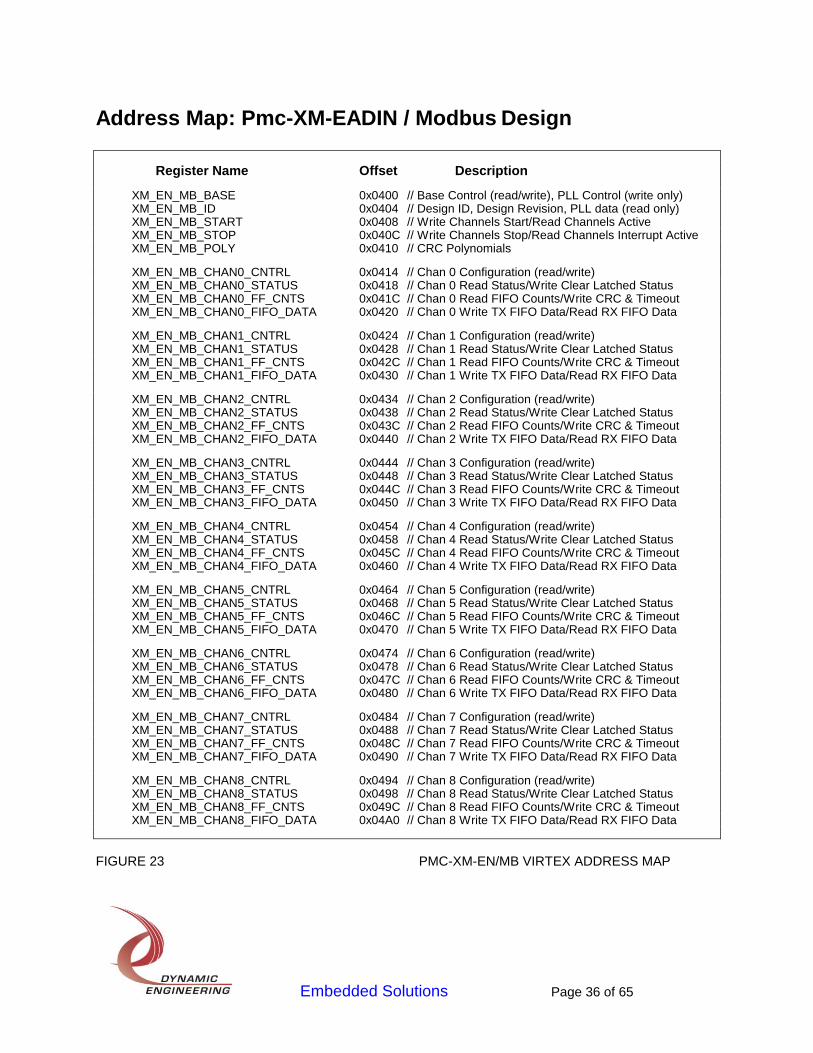
Address Map: Pmc-XM-EADIN / Modbus Design
Register Name Offset Description
XM_EN_MB_BASE 0x0400 // Base Control (read/write), PLL Control (write only) XM_EN_MB_ID 0x0404 // Design ID, Design Revision, PLL data (read only) XM_EN_MB_START 0x0408 // Write Channels Start/Read Channels Active XM_EN_MB_STOP 0x040C // Write Channels Stop/Read Channels Interrupt Active XM_EN_MB_POLY 0x0410 // CRC Polynomials
XM_EN_MB_CHAN0_CNTRL 0x0414 // Chan 0 Configuration (read/write) XM_EN_MB_CHAN0_STATUS 0x0418 // Chan 0 Read Status/Write Clear Latched Status XM_EN_MB_CHAN0_FF_CNTS 0x041C // Chan 0 Read FIFO Counts/Write CRC & Timeout XM_EN_MB_CHAN0_FIFO_DATA 0x0420 // Chan 0 Write TX FIFO Data/Read RX FIFO Data
XM_EN_MB_CHAN1_CNTRL 0x0424 // Chan 1 Configuration (read/write) XM_EN_MB_CHAN1_STATUS 0x0428 // Chan 1 Read Status/Write Clear Latched Status XM_EN_MB_CHAN1_FF_CNTS 0x042C // Chan 1 Read FIFO Counts/Write CRC & Timeout XM_EN_MB_CHAN1_FIFO_DATA 0x0430 // Chan 1 Write TX FIFO Data/Read RX FIFO Data
XM_EN_MB_CHAN2_CNTRL 0x0434 // Chan 2 Configuration (read/write) XM_EN_MB_CHAN2_STATUS 0x0438 // Chan 2 Read Status/Write Clear Latched Status XM_EN_MB_CHAN2_FF_CNTS 0x043C // Chan 2 Read FIFO Counts/Write CRC & Timeout XM_EN_MB_CHAN2_FIFO_DATA 0x0440 // Chan 2 Write TX FIFO Data/Read RX FIFO Data
XM_EN_MB_CHAN3_CNTRL 0x0444 // Chan 3 Configuration (read/write) XM_EN_MB_CHAN3_STATUS 0x0448 // Chan 3 Read Status/Write Clear Latched Status XM_EN_MB_CHAN3_FF_CNTS 0x044C // Chan 3 Read FIFO Counts/Write CRC & Timeout XM_EN_MB_CHAN3_FIFO_DATA 0x0450 // Chan 3 Write TX FIFO Data/Read RX FIFO Data
XM_EN_MB_CHAN4_CNTRL 0x0454 // Chan 4 Configuration (read/write) XM_EN_MB_CHAN4_STATUS 0x0458 // Chan 4 Read Status/Write Clear Latched Status XM_EN_MB_CHAN4_FF_CNTS 0x045C // Chan 4 Read FIFO Counts/Write CRC & Timeout XM_EN_MB_CHAN4_FIFO_DATA 0x0460 // Chan 4 Write TX FIFO Data/Read RX FIFO Data
XM_EN_MB_CHAN5_CNTRL 0x0464 // Chan 5 Configuration (read/write) XM_EN_MB_CHAN5_STATUS 0x0468 // Chan 5 Read Status/Write Clear Latched Status XM_EN_MB_CHAN5_FF_CNTS 0x046C // Chan 5 Read FIFO Counts/Write CRC & Timeout XM_EN_MB_CHAN5_FIFO_DATA 0x0470 // Chan 5 Write TX FIFO Data/Read RX FIFO Data
XM_EN_MB_CHAN6_CNTRL 0x0474 // Chan 6 Configuration (read/write) XM_EN_MB_CHAN6_STATUS 0x0478 // Chan 6 Read Status/Write Clear Latched Status XM_EN_MB_CHAN6_FF_CNTS 0x047C // Chan 6 Read FIFO Counts/Write CRC & Timeout XM_EN_MB_CHAN6_FIFO_DATA 0x0480 // Chan 6 Write TX FIFO Data/Read RX FIFO Data
XM_EN_MB_CHAN7_CNTRL 0x0484 // Chan 7 Configuration (read/write) XM_EN_MB_CHAN7_STATUS 0x0488 // Chan 7 Read Status/Write Clear Latched Status XM_EN_MB_CHAN7_FF_CNTS 0x048C // Chan 7 Read FIFO Counts/Write CRC & Timeout XM_EN_MB_CHAN7_FIFO_DATA 0x0490 // Chan 7 Write TX FIFO Data/Read RX FIFO Data
XM_EN_MB_CHAN8_CNTRL 0x0494 // Chan 8 Configuration (read/write) XM_EN_MB_CHAN8_STATUS 0x0498 // Chan 8 Read Status/Write Clear Latched Status XM_EN_MB_CHAN8_FF_CNTS 0x049C // Chan 8 Read FIFO Counts/Write CRC & Timeout XM_EN_MB_CHAN8_FIFO_DATA 0x04A0 // Chan 8 Write TX FIFO Data/Read RX FIFO Data
FIGURE 23 PMC-XM-EN/MB VIRTEX ADDRESS MAP

Embedded Solutions Page 37 of 65
XM_EN_MB_CHAN9_CNTRL 0x04A4 // Chan 9 Configuration (read/write) XM_EN_MB_CHAN9_STATUS 0x04A8 // Chan 9 Read Status/Write Clear Latched Status XM_EN_MB_CHAN9_FF_CNTS 0x04AC // Chan 9 Read FIFO Counts/Write CRC & Timeout XM_EN_MB_CHAN9_FIFO_DATA 0x04B0 // Chan 9 Write TX FIFO Data/Read RX FIFO Data
XM_EN_MB_CHAN10_CNTRL 0x04B4 // Chan 10 Configuration (read/write) XM_EN_MB_CHAN10_STATUS 0x04B8 // Chan 10 Read Status/Write Clear Latched Status XM_EN_MB_CHAN10_FF_CNTS 0x04BC // Chan 10 Read FIFO Counts/Write CRC & Timeout XM_EN_MB_CHAN10_FIFO_DATA 0x04C0 // Chan 10 Write TX FIFO Data/Read RX FIFO Data
XM_EN_MB_CHAN11_CNTRL 0x04C4 // Chan 11 Configuration (read/write) XM_EN_MB_CHAN11_STATUS 0x04C8 // Chan 11 Read Status/Write Clear Latched Status XM_EN_MB_CHAN11_FF_CNTS 0x04CC // Chan 11 Read FIFO Counts/Write CRC & Timeout XM_EN_MB_CHAN11_FIFO_DATA 0x04D0 // Chan 11 Write TX FIFO Data/Read RX FIFO Data
XM_EN_MB_CHAN12_CNTRL 0x04D4 // Chan 12 Configuration (read/write) XM_EN_MB_CHAN12_STATUS 0x04D8 // Chan 12 Read Status/Write Clear Latched Status XM_EN_MB_CHAN12_FF_CNTS 0x04DC // Chan 12 Read FIFO Counts/Write CRC & Timeout XM_EN_MB_CHAN12_FIFO_DATA 0x04E0 // Chan 12 Write TX FIFO Data/Read RX FIFO Data
XM_EN_MB_CHAN13_CNTRL 0x04E4 // Chan 13 Configuration (read/write) XM_EN_MB_CHAN13_STATUS 0x04E8 // Chan 13 Read Status/Write Clear Latched Status XM_EN_MB_CHAN13_FF_CNTS 0x04EC // Chan 13 Read FIFO Counts/Write CRC & Timeout XM_EN_MB_CHAN13_FIFO_DATA 0x04F0 // Chan 13 Write TX FIFO Data/Read RX FIFO Data
XM_EN_MB_CHAN14_CNTRL 0x04F4 // Chan 14 Configuration (read/write) XM_EN_MB_CHAN14_STATUS 0x04F8 // Chan 14 Read Status/Write Clear Latched Status XM_EN_MB_CHAN14_FF_CNTS 0x04FC // Chan 14 Read FIFO Counts/Write CRC & Timeout XM_EN_MB_CHAN14_FIFO_DATA 0x0500 // Chan 14 Write TX FIFO Data/Read RX FIFO Data
XM_EN_MB_CHAN15_CNTRL 0x0500 // Chan 15 Configuration (read/write) XM_EN_MB_CHAN15_STATUS 0x0500 // Chan 15 Read Status/Write Clear Latched Status XM_EN_MB_CHAN15_FF_CNTS 0x0500 // Chan 15 Read FIFO Counts/Write CRC & Timeout XM_EN_MB_CHAN15_FIFO_DATA 0x0510 // Chan 15 Write TX FIFO Data/Read RX FIFO Data
XM_EN_MB_CHAN16_CNTRL 0x0514 // Chan 16 Configuration (read/write) XM_EN_MB_CHAN16_STATUS 0x0518 // Chan 16 Read Status/Write Clear Latched Status XM_EN_MB_CHAN16_FF_CNTS 0x051C // Chan 16 Read FIFO Counts/Write CRC & Timeout XM_EN_MB_CHAN16_FIFO_DATA 0x0520 // Chan 16 Write TX FIFO Data/Read RX FIFO Data
XM_EN_MB_CHAN17_CNTRL 0x0524 // Chan 17 Configuration (read/write) XM_EN_MB_CHAN17_STATUS 0x0528 // Chan 17 Read Status/Write Clear Latched Status XM_EN_MB_CHAN17_FF_CNTS 0x052C // Chan 17 Read FIFO Counts/Write CRC & Timeout XM_EN_MB_CHAN17_FIFO_DATA 0x0530 // Chan 17 Write TX FIFO Data/Read RX FIFO Data
XM_EN_MB_CHAN18_CNTRL 0x0534 // Chan 18 Configuration (read/write) XM_EN_MB_CHAN18_STATUS 0x0538 // Chan 18 Read Status/Write Clear Latched Status XM_EN_MB_CHAN18_FF_CNTS 0x053C // Chan 18 Read FIFO Counts/Write CRC & Timeout XM_EN_MB_CHAN18_FIFO_DATA 0x0540 // Chan 18 Write TX FIFO Data/Read RX FIFO Data|
XM_EN_MB_CHAN19_CNTRL 0x0544 // Chan 19 Configuration (read/write) XM_EN_MB_CHAN19_STATUS 0x0548 // Chan 19 Read Status/Write Clear Latched Status XM_EN_MB_CHAN19_FF_CNTS 0x054C // Chan 19 Read FIFO Counts/Write CRC & Timeout XM_EN_MB_CHAN19_FIFO_DATA 0x0550 // Chan 19 Write TX FIFO Data/Read RX FIFO Data
XM_EN_MB_CHAN20_CNTRL 0x0554 // Chan 20 Configuration (read/write) XM_EN_MB_CHAN20_STATUS 0x0558 // Chan 20 Read Status/Write Clear Latched Status XM_EN_MB_CHAN20_FF_CNTS 0x055C // Chan 20 Read FIFO Counts/Write CRC & Timeout XM_EN_MB_CHAN20_FIFO_DATA 0x0560 // Chan 20 Write TX FIFO Data/Read RX FIFO Data
FIGURE 23 (CONTINUED) PMC-XM-EN/MB VIRTEX ADDRESS MAP
Embedded Solutions Page 38 of 65
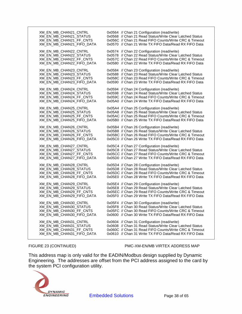
XM_EN_MB_CHAN21_CNTRL 0x0564 // Chan 21 Configuration (read/write) XM_EN_MB_CHAN21_STATUS 0x0568 // Chan 21 Read Status/Write Clear Latched Status XM_EN_MB_CHAN21_FF_CNTS 0x056C // Chan 21 Read FIFO Counts/Write CRC & Timeout XM_EN_MB_CHAN21_FIFO_DATA 0x0570 // Chan 21 Write TX FIFO Data/Read RX FIFO Data
XM_EN_MB_CHAN22_CNTRL 0x0574 // Chan 22 Configuration (read/write) XM_EN_MB_CHAN22_STATUS 0x0578 // Chan 22 Read Status/Write Clear Latched Status XM_EN_MB_CHAN22_FF_CNTS 0x057C // Chan 22 Read FIFO Counts/Write CRC & Timeout XM_EN_MB_CHAN22_FIFO_DATA 0x0580 // Chan 22 Write TX FIFO Data/Read RX FIFO Data
XM_EN_MB_CHAN23_CNTRL 0x0584 // Chan 23 Configuration (read/write) XM_EN_MB_CHAN23_STATUS 0x0588 // Chan 23 Read Status/Write Clear Latched Status XM_EN_MB_CHAN23_FF_CNTS 0x058C // Chan 23 Read FIFO Counts/Write CRC & Timeout XM_EN_MB_CHAN23_FIFO_DATA 0x0590 // Chan 23 Write TX FIFO Data/Read RX FIFO Data
XM_EN_MB_CHAN24_CNTRL 0x0594 // Chan 24 Configuration (read/write) XM_EN_MB_CHAN24_STATUS 0x0598 // Chan 24 Read Status/Write Clear Latched Status XM_EN_MB_CHAN24_FF_CNTS 0x059C // Chan 24 Read FIFO Counts/Write CRC & Timeout XM_EN_MB_CHAN24_FIFO_DATA 0x05A0 // Chan 24 Write TX FIFO Data/Read RX FIFO Data
XM_EN_MB_CHAN25_CNTRL 0x05A4 // Chan 25 Configuration (read/write) XM_EN_MB_CHAN25_STATUS 0x05A8 // Chan 25 Read Status/Write Clear Latched Status XM_EN_MB_CHAN25_FF_CNTS 0x05AC // Chan 25 Read FIFO Counts/Write CRC & Timeout XM_EN_MB_CHAN25_FIFO_DATA 0x05B0 // Chan 25 Write TX FIFO Data/Read RX FIFO Data
XM_EN_MB_CHAN26_CNTRL 0x05B4 // Chan 26 Configuration (read/write) XM_EN_MB_CHAN26_STATUS 0x05B8 // Chan 26 Read Status/Write Clear Latched Status XM_EN_MB_CHAN26_FF_CNTS 0x05BC // Chan 26 Read FIFO Counts/Write CRC & Timeout XM_EN_MB_CHAN26_FIFO_DATA 0x05C0 // Chan 26 Write TX FIFO Data/Read RX FIFO Data
XM_EN_MB_CHAN27_CNTRL 0x05C4 // Chan 27 Configuration (read/write) XM_EN_MB_CHAN27_STATUS 0x05C8 // Chan 27 Read Status/Write Clear Latched Status XM_EN_MB_CHAN27_FF_CNTS 0x05CC // Chan 27 Read FIFO Counts/Write CRC & Timeout XM_EN_MB_CHAN27_FIFO_DATA 0x05D0 // Chan 27 Write TX FIFO Data/Read RX FIFO Data
XM_EN_MB_CHAN28_CNTRL 0x05D4 // Chan 28 Configuration (read/write) XM_EN_MB_CHAN28_STATUS 0x05D8 // Chan 28 Read Status/Write Clear Latched Status XM_EN_MB_CHAN28_FF_CNTS 0x05DC // Chan 28 Read FIFO Counts/Write CRC & Timeout XM_EN_MB_CHAN28_FIFO_DATA 0x05E0 // Chan 28 Write TX FIFO Data/Read RX FIFO Data
XM_EN_MB_CHAN29_CNTRL 0x05E4 // Chan 29 Configuration (read/write) XM_EN_MB_CHAN29_STATUS 0x05E8 // Chan 29 Read Status/Write Clear Latched Status XM_EN_MB_CHAN29_FF_CNTS 0x05EC // Chan 29 Read FIFO Counts/Write CRC & Timeout XM_EN_MB_CHAN29_FIFO_DATA 0x05F0 // Chan 29 Write TX FIFO Data/Read RX FIFO Data
XM_EN_MB_CHAN30_CNTRL 0x05F4 // Chan 30 Configuration (read/write) XM_EN_MB_CHAN30_STATUS 0x05F8 // Chan 30 Read Status/Write Clear Latched Status XM_EN_MB_CHAN30_FF_CNTS 0x05FC // Chan 30 Read FIFO Counts/Write CRC & Timeout XM_EN_MB_CHAN30_FIFO_DATA 0x0600 // Chan 30 Write TX FIFO Data/Read RX FIFO Data
XM_EN_MB_CHAN31_CNTRL 0x0604 // Chan 31 Configuration (read/write) XM_EN_MB_CHAN31_STATUS 0x0608 // Chan 31 Read Status/Write Clear Latched Status XM_EN_MB_CHAN31_FF_CNTS 0x060C // Chan 31 Read FIFO Counts/Write CRC & Timeout XM_EN_MB_CHAN31_FIFO_DATA 0x0610 // Chan 31 Write TX FIFO Data/Read RX FIFO Data
FIGURE 23 (CONTINUED) PMC-XM-EN/MB VIRTEX ADDRESS MAP
This address map is only valid for the EADIN/Modbus design supplied by Dynamic Engineering. The addresses are offset from the PCI address assigned to the card by the system PCI configuration utility.
Embedded Solutions Page 39 of 65
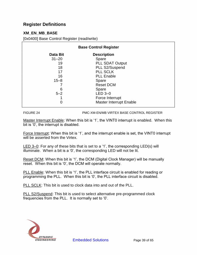
Register Definitions
XM_EN_MB_BASE
[0x0400] Base Control Register (read/write)
Base Control Register
Data Bit Description 31–20 Spare 19 PLL SDAT Output 18 PLL S2/Suspend 17 PLL SCLK 16 PLL Enable 15–8 Spare 7 Reset DCM 6 Spare 5–2 LED 3–0 1 Force Interrupt 0 Master Interrupt Enable
FIGURE 24 PMC-XM-EN/MB VIRTEX BASE CONTROL REGISTER
Master Interrupt Enable: When this bit is ‘1’, the VINT0 interrupt is enabled. When this bit is ‘0’, the interrupt is disabled. Force Interrupt: When this bit is ‘1’, and the interrupt enable is set, the VINT0 interrupt will be asserted from the Virtex. LED 3–0: For any of these bits that is set to a ‘1’, the corresponding LED(s) will illuminate. When a bit is a ‘0’, the corresponding LED will not be lit. Reset DCM: When this bit is ‘1’, the DCM (Digital Clock Manager) will be manually reset. When this bit is ‘0’, the DCM will operate normally. PLL Enable: When this bit is ‘1’, the PLL interface circuit is enabled for reading or programming the PLL. When this bit is ‘0’, the PLL interface circuit is disabled. PLL SCLK: This bit is used to clock data into and out of the PLL. PLL S2/Suspend: This bit is used to select alternative pre-programmed clock frequencies from the PLL. It is normally set to ‘0’.

Embedded Solutions Page 40 of 65
PLL SDAT Output: This is where the PLL data state is specified when data is being written to the PLL. When the bus is turned around and the PLL is driving the data line this bit must be set to a ‘1’. The PMC-XM has a PLL device which is programmed over an I
2C bus to produce the
desired frequencies. The data line has a pull-up on the board. When the PLL is enabled and the I
2C data bit
is set to ‘0’ in this register, the external line is driven low. When not enabled or when the I
2C data bit is set to ‘1’ in this register, the external line is tri-stated and pulled-up by
the resistor. For a read operation the data should be set to ‘1’ to allow the PLL to drive the data line. The clock line for the PLL is toggled along with the data to create a bit stream with a “software clock”. Set the bit to the next state and toggle the clock line and repeat. The upper selection bit can be set in the register and directly driven to the PLL. This allows the selection of alternative pre-programmed clock frequencies. To read over the I
2C bus a command is first written and then the bus read for the
response. The I2C data input bit in the ID register contains the state of the bus when
read. The software will toggle the clock line and when the low-to-high transition is made, read the data bit then repeat until the entire message is captured. The engineering kit contains the logic and software required to program the PLL and to read-back the internal register programming. The software to determine the frequency command words is available from Cypress Semiconductor. The PLL part number is CY22393FC. Cypress has a utility available for calculating the frequency command words for the PLL. http://www.dyneng.com/CyberClocks.zip is the URL for the Cypress software used to calculate the PLL programming words. The reference frequency is 40 MHz.
Embedded Solutions Page 41 of 65
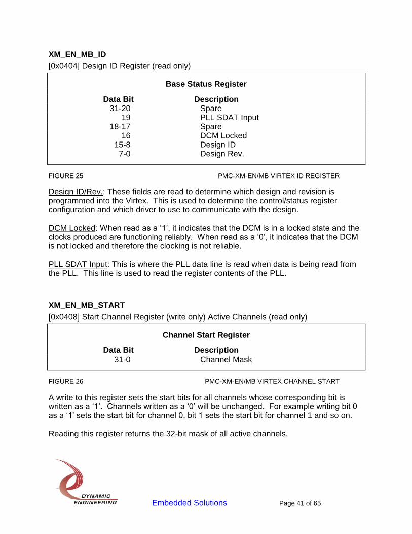
XM_EN_MB_ID
[0x0404] Design ID Register (read only)
Base Status Register
Data Bit Description 31-20 Spare 19 PLL SDAT Input 18-17 Spare 16 DCM Locked 15-8 Design ID 7-0 Design Rev.
FIGURE 25 PMC-XM-EN/MB VIRTEX ID REGISTER
Design ID/Rev.: These fields are read to determine which design and revision is programmed into the Virtex. This is used to determine the control/status register configuration and which driver to use to communicate with the design. DCM Locked: When read as a ‘1’, it indicates that the DCM is in a locked state and the clocks produced are functioning reliably. When read as a ‘0’, it indicates that the DCM is not locked and therefore the clocking is not reliable. PLL SDAT Input: This is where the PLL data line is read when data is being read from the PLL. This line is used to read the register contents of the PLL.
XM_EN_MB_START
[0x0408] Start Channel Register (write only) Active Channels (read only)
Channel Start Register
Data Bit Description 31-0 Channel Mask
FIGURE 26 PMC-XM-EN/MB VIRTEX CHANNEL START
A write to this register sets the start bits for all channels whose corresponding bit is written as a ‘1’. Channels written as a ‘0’ will be unchanged. For example writing bit 0 as a ‘1’ sets the start bit for channel 0, bit 1 sets the start bit for channel 1 and so on. Reading this register returns the 32-bit mask of all active channels.
Embedded Solutions Page 42 of 65
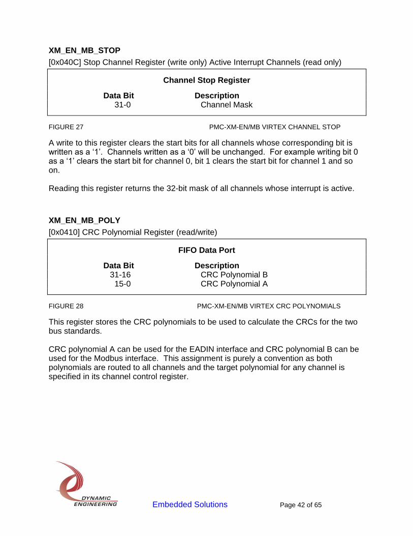
XM_EN_MB_STOP
[0x040C] Stop Channel Register (write only) Active Interrupt Channels (read only)
Channel Stop Register
Data Bit Description 31-0 Channel Mask
FIGURE 27 PMC-XM-EN/MB VIRTEX CHANNEL STOP
A write to this register clears the start bits for all channels whose corresponding bit is written as a ‘1’. Channels written as a ‘0’ will be unchanged. For example writing bit 0 as a ‘1’ clears the start bit for channel 0, bit 1 clears the start bit for channel 1 and so on. Reading this register returns the 32-bit mask of all channels whose interrupt is active.
XM_EN_MB_POLY
[0x0410] CRC Polynomial Register (read/write)
FIFO Data Port
Data Bit Description 31-16 CRC Polynomial B 15-0 CRC Polynomial A
FIGURE 28 PMC-XM-EN/MB VIRTEX CRC POLYNOMIALS
This register stores the CRC polynomials to be used to calculate the CRCs for the two bus standards. CRC polynomial A can be used for the EADIN interface and CRC polynomial B can be used for the Modbus interface. This assignment is purely a convention as both polynomials are routed to all channels and the target polynomial for any channel is specified in its channel control register.
Embedded Solutions Page 43 of 65
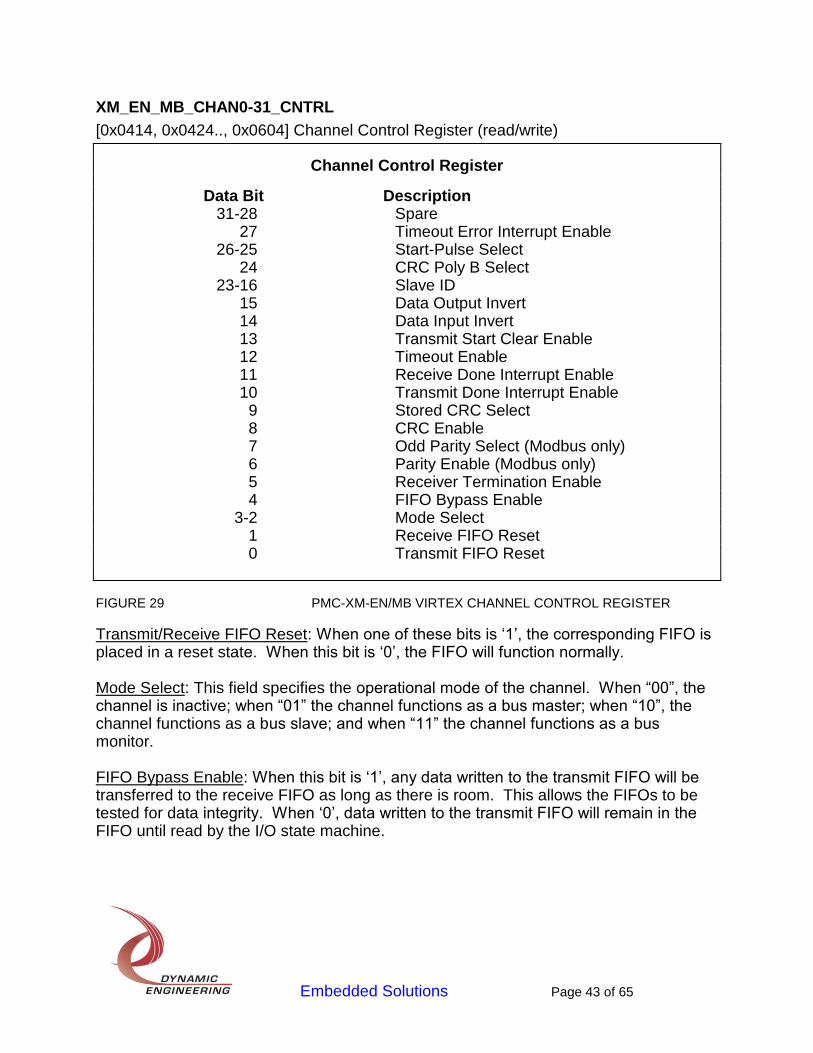
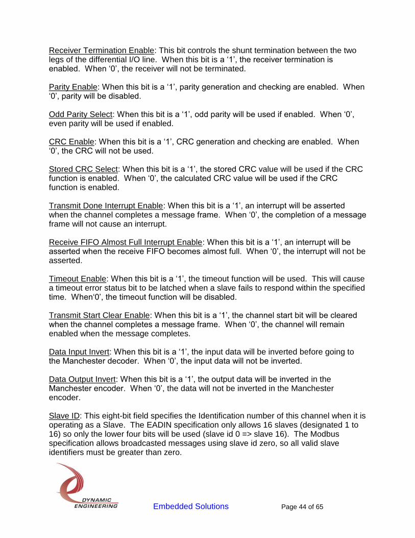
XM_EN_MB_CHAN0-31_CNTRL
[0x0414, 0x0424.., 0x0604] Channel Control Register (read/write)
Channel Control Register
Data Bit Description 31-28 Spare 27 Timeout Error Interrupt Enable 26-25 Start-Pulse Select 24 CRC Poly B Select 23-16 Slave ID 15 Data Output Invert 14 Data Input Invert 13 Transmit Start Clear Enable 12 Timeout Enable 11 Receive Done Interrupt Enable 10 Transmit Done Interrupt Enable 9 Stored CRC Select 8 CRC Enable 7 Odd Parity Select (Modbus only) 6 Parity Enable (Modbus only) 5 Receiver Termination Enable 4 FIFO Bypass Enable 3-2 Mode Select 1 Receive FIFO Reset 0 Transmit FIFO Reset
FIGURE 29 PMC-XM-EN/MB VIRTEX CHANNEL CONTROL REGISTER
Transmit/Receive FIFO Reset: When one of these bits is ‘1’, the corresponding FIFO is placed in a reset state. When this bit is ‘0’, the FIFO will function normally. Mode Select: This field specifies the operational mode of the channel. When “00”, the channel is inactive; when “01” the channel functions as a bus master; when “10”, the channel functions as a bus slave; and when “11” the channel functions as a bus monitor. FIFO Bypass Enable: When this bit is ‘1’, any data written to the transmit FIFO will be transferred to the receive FIFO as long as there is room. This allows the FIFOs to be tested for data integrity. When ‘0’, data written to the transmit FIFO will remain in the FIFO until read by the I/O state machine.
Embedded Solutions Page 44 of 65
Receiver Termination Enable: This bit controls the shunt termination between the two legs of the differential I/O line. When this bit is a ‘1’, the receiver termination is enabled. When ‘0’, the receiver will not be terminated. Parity Enable: When this bit is a ‘1’, parity generation and checking are enabled. When ‘0’, parity will be disabled. Odd Parity Select: When this bit is a ‘1’, odd parity will be used if enabled. When ‘0’, even parity will be used if enabled. CRC Enable: When this bit is a ‘1’, CRC generation and checking are enabled. When ‘0’, the CRC will not be used. Stored CRC Select: When this bit is a ‘1’, the stored CRC value will be used if the CRC function is enabled. When ‘0’, the calculated CRC value will be used if the CRC function is enabled. Transmit Done Interrupt Enable: When this bit is a ‘1’, an interrupt will be asserted when the channel completes a message frame. When ‘0’, the completion of a message frame will not cause an interrupt. Receive FIFO Almost Full Interrupt Enable: When this bit is a ‘1’, an interrupt will be asserted when the receive FIFO becomes almost full. When ‘0’, the interrupt will not be asserted. Timeout Enable: When this bit is a ‘1’, the timeout function will be used. This will cause a timeout error status bit to be latched when a slave fails to respond within the specified time. When‘0’, the timeout function will be disabled. Transmit Start Clear Enable: When this bit is a ‘1’, the channel start bit will be cleared when the channel completes a message frame. When ‘0’, the channel will remain enabled when the message completes. Data Input Invert: When this bit is a ‘1’, the input data will be inverted before going to the Manchester decoder. When ‘0’, the input data will not be inverted. Data Output Invert: When this bit is a ‘1’, the output data will be inverted in the Manchester encoder. When ‘0’, the data will not be inverted in the Manchester encoder. Slave ID: This eight-bit field specifies the Identification number of this channel when it is operating as a Slave. The EADIN specification only allows 16 slaves (designated 1 to 16) so only the lower four bits will be used (slave id 0 => slave 16). The Modbus specification allows broadcasted messages using slave id zero, so all valid slave identifiers must be greater than zero.
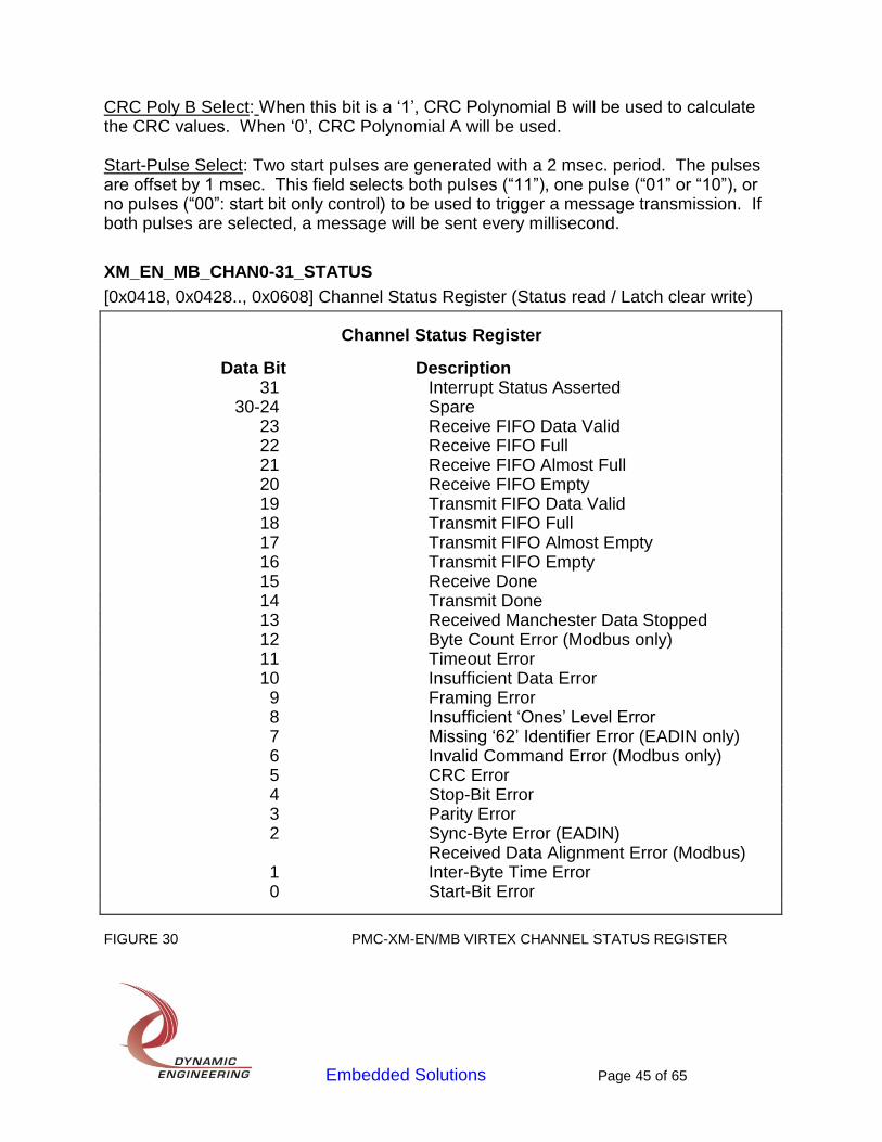
Embedded Solutions Page 45 of 65
CRC Poly B Select: When this bit is a ‘1’, CRC Polynomial B will be used to calculate the CRC values. When ‘0’, CRC Polynomial A will be used. Start-Pulse Select: Two start pulses are generated with a 2 msec. period. The pulses are offset by 1 msec. This field selects both pulses (“11”), one pulse (“01” or “10”), or no pulses (“00”: start bit only control) to be used to trigger a message transmission. If both pulses are selected, a message will be sent every millisecond.
XM_EN_MB_CHAN0-31_STATUS
[0x0418, 0x0428.., 0x0608] Channel Status Register (Status read / Latch clear write)
Channel Status Register
Data Bit Description 31 Interrupt Status Asserted 30-24 Spare 23 Receive FIFO Data Valid 22 Receive FIFO Full 21 Receive FIFO Almost Full 20 Receive FIFO Empty 19 Transmit FIFO Data Valid 18 Transmit FIFO Full 17 Transmit FIFO Almost Empty 16 Transmit FIFO Empty 15 Receive Done 14 Transmit Done 13 Received Manchester Data Stopped 12 Byte Count Error (Modbus only) 11 Timeout Error 10 Insufficient Data Error 9 Framing Error 8 Insufficient ‘Ones’ Level Error 7 Missing ‘62’ Identifier Error (EADIN only) 6 Invalid Command Error (Modbus only) 5 CRC Error 4 Stop-Bit Error 3 Parity Error 2 Sync-Byte Error (EADIN) Received Data Alignment Error (Modbus) 1 Inter-Byte Time Error 0 Start-Bit Error
FIGURE 30 PMC-XM-EN/MB VIRTEX CHANNEL STATUS REGISTER
Embedded Solutions Page 46 of 65
Start-Bit Error: When a one is read, it indicates that a Manchester error occurred while a start bit was being received. A zero indicates that no error occurred while a start bit was being received. This is a latched bit and must be cleared by writing a ‘1’ to bit 0 at this address. Inter-Byte Time Error: When a one is read, it indicates that the gap between consecutive bytes in the message frame was too long. A zero indicates that this gap was within spec. This is a latched bit and must be cleared by writing a ‘1’ to bit 1 at this address. Sync-Byte Error: (EADIN) When a one is read, it indicates that a received sync-byte was incorrect (not 0x55). A zero indicates that all the sync bytes were correct. This is a latched bit and must be cleared by writing a ‘1’ to bit 2 at this address. Received Data Alignment Error: (Modbus) When a one is read, it indicates that a byte-wide item was stored in the upper byte of a 16-bit data-word. All byte fields should be stored in the lower byte of a 16-bit data-word with the upper byte containing zeros. A zero indicates that all byte-wide items were stored correctly. This is a latched bit and must be cleared by writing a ‘1’ to bit 2 at this address. Parity Error: When a one is read, it indicates that a parity error was detected. A zero indicates that no parity error was detected. This is a latched bit and must be cleared by writing a ‘1’ to bit 3 at this address. Stop-Bit Error: When a one is read, it indicates that a received byte’s stop bit was low. A zero indicates that all received byte’s stop bits were high. This is a latched bit and must be cleared by writing a ‘1’ to bit 4 at this address. CRC Error: When a one is read, it indicates that a CRC error occurred i.e. the calculated CRC did not match the received CRC. A zero indicates that a CRC error did not occur. This is a latched bit and must be cleared by writing a ‘1’ to bit 5 at this address. Invalid Command Error: When a one is read, it indicates that a command byte received was not one of the supported commands. This status is used by the Modbus interface only. A zero indicates that all received commands are supported. This is a latched bit and must be cleared by writing a ‘1’ to bit 6 at this address. This bit is valid for Modbus only. Missing ‘62’ Identifier Error: When a one is read, it indicates that the PID in a user defined frame was not a decimal 62 as required by the EADIN specification. A zero indicates that the user defined PIDs were correctly received. This is a latched bit and must be cleared by writing a ‘1’ to bit 7 at this address. This bit is valid for EADIN only.

Embedded Solutions Page 47 of 65
Insufficient ‘Ones’ Level Error: When a one is read, it indicates that there were an insufficient number of ‘1’ bits before the break was received. This status is used by the EADIN interface only. A zero indicates that the number of ‘1’ bits was sufficient. This is a latched bit and must be cleared by writing a ‘1’ to bit 8 at this address. Framing Error: When a one is read, it indicates that there was an error in the received frame structure or byte framing. A zero indicates that no such error occurred. This is a latched bit and must be cleared by writing a ‘1’ to bit 9 at this address. Insufficient Transmit Data Error: When a one is read, it indicates that there was insufficient data in the transmit FIFO to complete the current message frame. A zero indicates that there was enough data to complete the frame. This is a latched bit and must be cleared by writing a ‘1’ to bit 10 at this address. Timeout Error: When a one is read, it indicates that the targeted slave did not respond within the specified time. A zero indicates that the slave responded within the allotted time. This is a latched bit and must be cleared by writing a ‘1’ to bit 11 at this address. Byte Count Error: When a one is read, it indicates that the byte count field in a command was not consistent with the word-count field. This status is used by the Modbus interface only. A zero indicates that the byte-count and word-count were consistent. This is a latched bit and must be cleared by writing a ‘1’ to bit 12 at this address. This bit is valid for Modbus only. Received Manchester Data Stopped: When a one is read, it indicates that the Manchester decoder is no longer receiving Manchester encoded data. A zero indicates that Manchester data is still being received. This is the real-time received data state. Transmit Done: When a one is read, it indicates that a message transmission has completed. A zero indicates that no transmitted message has completed since the bit was last cleared. This is a latched bit and must be cleared by writing a ‘1’ to bit 14 at this address. Receive Done: When a one is read, it indicates that a message has been received by the slave node. A zero indicates that no received message has completed since the bit was last cleared. . This is a latched bit and must be cleared by writing a ‘1’ to bit 15 at this address. Transmit FIFO Empty: When a one is read, it indicates that the corresponding transmit FIFO is empty. A zero indicates that the FIFO has at least one word in it. Transmit FIFO Almost Empty: When a one is read, it indicates that there is only one word left in the transmit FIFO. A zero indicates that there is more than one word in the FIFO.
Embedded Solutions Page 48 of 65
Transmit FIFO Full: When a one is read, it indicates that the corresponding transmit FIFO is full. A zero indicates that there is room for at least one more word in the FIFO. Transmit FIFO Data Valid: When a one is read, it indicates that there is valid transmit data. This can be true even if the FIFO is empty because there is a holding latch at the FIFO output. A zero indicates that there is no valid transmit data available. Receive FIFO Empty: When a one is read, it indicates that the corresponding receive FIFO is empty. A zero indicates that the FIFO has at least one word in it. Receive FIFO Almost Full: When a one is read, it indicates that the corresponding receive FIFO is one word less than full. A zero indicates that there is still room for more than one word in the FIFO. Receive FIFO Full: When a one is read, it indicates that the corresponding receive FIFO is full. A zero indicates that there is room for at least one more word in the FIFO. Receive FIFO Data Valid: When a one is read, it indicates that there is valid receive data. This can be true even if the FIFO is empty because there is a holding latch at the FIFO output. A zero indicates that there is no valid receive data available. Interrupt Status Asserted: When a one is read, it indicates that an enabled interrupt condition is active. This will cause a system interrupt to be asserted if the necessary interrupt enables are asserted. A zero indicates that no enabled interrupt conditions are active.
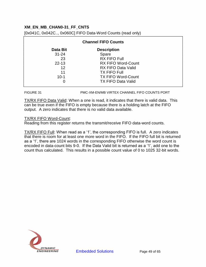
Embedded Solutions Page 49 of 65
XM_EN_MB_CHAN0-31_FF_CNTS
[0x041C, 0x042C.., 0x060C] FIFO Data-Word Counts (read only)
Channel FIFO Counts
Data Bit Description 31-24 Spare 23 RX FIFO Full 22-13 RX FIFO Word-Count 12 RX FIFO Data Valid 11 TX FIFO Full 10-1 TX FIFO Word-Count 0 TX FIFO Data Valid
FIGURE 31 PMC-XM-EN/MB VIRTEX CHANNEL FIFO COUNTS PORT
TX/RX FIFO Data Valid: When a one is read, it indicates that there is valid data. This can be true even if the FIFO is empty because there is a holding latch at the FIFO output. A zero indicates that there is no valid data available. TX/RX FIFO Word-Count: Reading from this register returns the transmit/receive FIFO data-word counts. TX/RX FIFO Full: When read as a ‘1’, the corresponding FIFO is full. A zero indicates that there is room for at least one more word in the FIFO. If the FIFO full bit is returned as a ‘1’, there are 1024 words in the corresponding FIFO otherwise the word count is encoded in data-count bits 9-0. If the Data Valid bit is returned as a ‘1’, add one to the count thus calculated. This results in a possible count value of 0 to 1025 32-bit words.
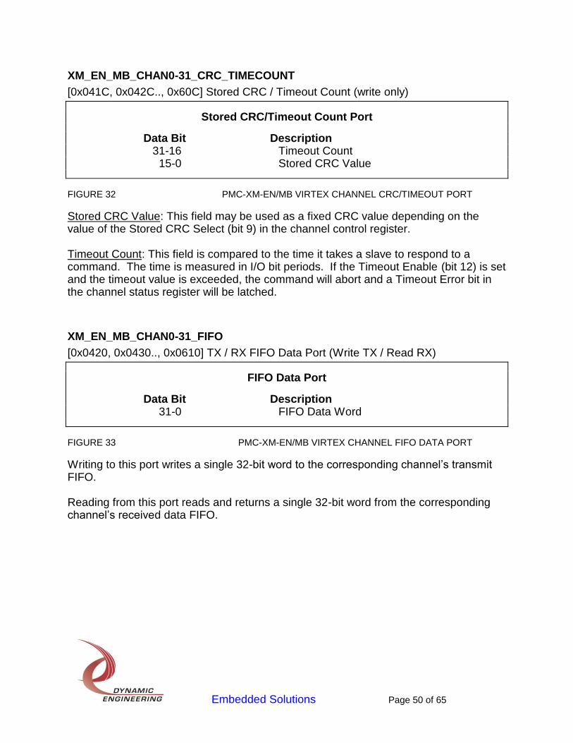
Embedded Solutions Page 50 of 65
XM_EN_MB_CHAN0-31_CRC_TIMECOUNT
[0x041C, 0x042C.., 0x60C] Stored CRC / Timeout Count (write only)
Stored CRC/Timeout Count Port
Data Bit Description 31-16 Timeout Count 15-0 Stored CRC Value
FIGURE 32 PMC-XM-EN/MB VIRTEX CHANNEL CRC/TIMEOUT PORT
Stored CRC Value: This field may be used as a fixed CRC value depending on the value of the Stored CRC Select (bit 9) in the channel control register. Timeout Count: This field is compared to the time it takes a slave to respond to a command. The time is measured in I/O bit periods. If the Timeout Enable (bit 12) is set and the timeout value is exceeded, the command will abort and a Timeout Error bit in the channel status register will be latched.
XM_EN_MB_CHAN0-31_FIFO
[0x0420, 0x0430.., 0x0610] TX / RX FIFO Data Port (Write TX / Read RX)
FIFO Data Port
Data Bit Description 31-0 FIFO Data Word
FIGURE 33 PMC-XM-EN/MB VIRTEX CHANNEL FIFO DATA PORT
Writing to this port writes a single 32-bit word to the corresponding channel’s transmit FIFO. Reading from this port reads and returns a single 32-bit word from the corresponding channel’s received data FIFO.
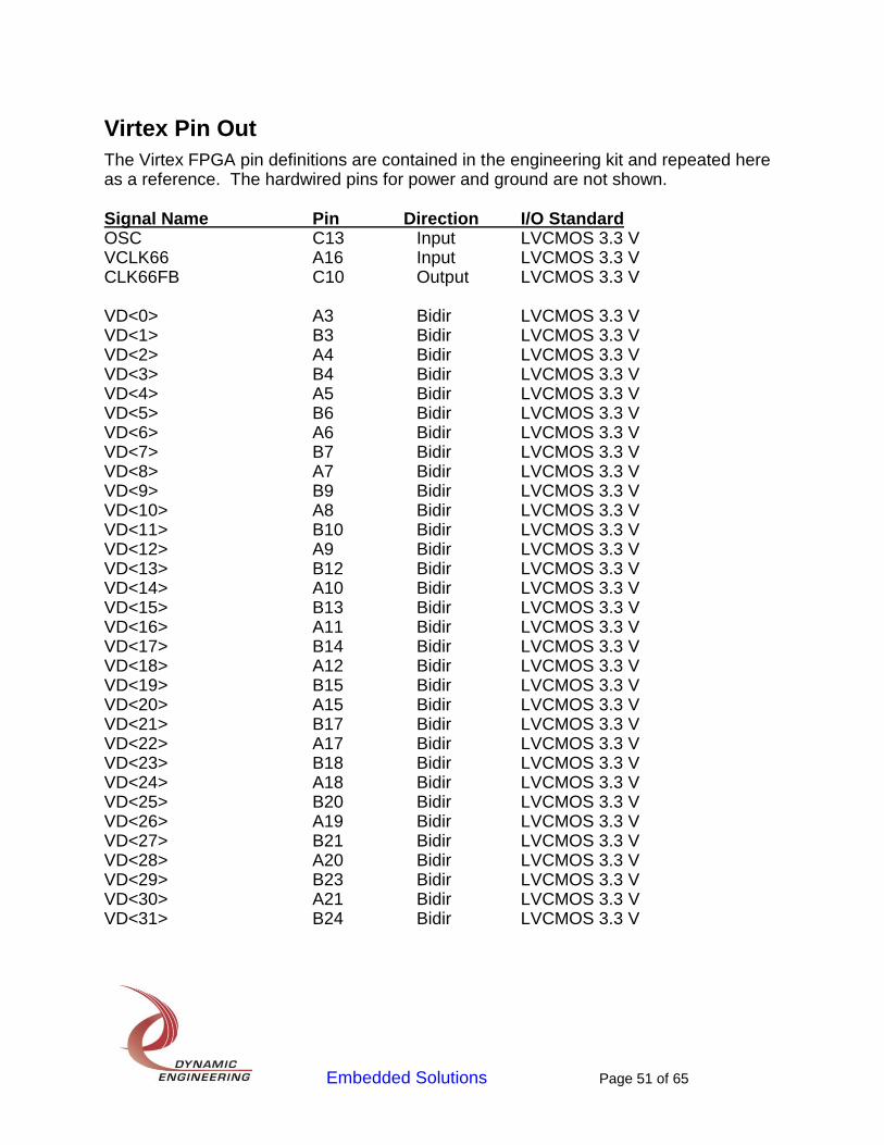
Embedded Solutions Page 51 of 65
Virtex Pin Out
The Virtex FPGA pin definitions are contained in the engineering kit and repeated here as a reference. The hardwired pins for power and ground are not shown. Signal Name Pin Direction I/O Standard OSC C13 Input LVCMOS 3.3 V VCLK66 A16 Input LVCMOS 3.3 V CLK66FB C10 Output LVCMOS 3.3 V VD<0> A3 Bidir LVCMOS 3.3 V VD<1> B3 Bidir LVCMOS 3.3 V VD<2> A4 Bidir LVCMOS 3.3 V VD<3> B4 Bidir LVCMOS 3.3 V VD<4> A5 Bidir LVCMOS 3.3 V VD<5> B6 Bidir LVCMOS 3.3 V VD<6> A6 Bidir LVCMOS 3.3 V VD<7> B7 Bidir LVCMOS 3.3 V VD<8> A7 Bidir LVCMOS 3.3 V VD<9> B9 Bidir LVCMOS 3.3 V VD<10> A8 Bidir LVCMOS 3.3 V VD<11> B10 Bidir LVCMOS 3.3 V VD<12> A9 Bidir LVCMOS 3.3 V VD<13> B12 Bidir LVCMOS 3.3 V VD<14> A10 Bidir LVCMOS 3.3 V VD<15> B13 Bidir LVCMOS 3.3 V VD<16> A11 Bidir LVCMOS 3.3 V VD<17> B14 Bidir LVCMOS 3.3 V VD<18> A12 Bidir LVCMOS 3.3 V VD<19> B15 Bidir LVCMOS 3.3 V VD<20> A15 Bidir LVCMOS 3.3 V VD<21> B17 Bidir LVCMOS 3.3 V VD<22> A17 Bidir LVCMOS 3.3 V VD<23> B18 Bidir LVCMOS 3.3 V VD<24> A18 Bidir LVCMOS 3.3 V VD<25> B20 Bidir LVCMOS 3.3 V VD<26> A19 Bidir LVCMOS 3.3 V VD<27> B21 Bidir LVCMOS 3.3 V VD<28> A20 Bidir LVCMOS 3.3 V VD<29> B23 Bidir LVCMOS 3.3 V VD<30> A21 Bidir LVCMOS 3.3 V VD<31> B24 Bidir LVCMOS 3.3 V
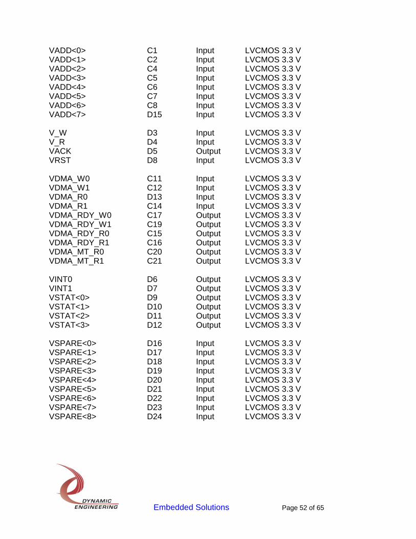
Embedded Solutions Page 52 of 65
VADD<0> C1 Input LVCMOS 3.3 V VADD<1> C2 Input LVCMOS 3.3 V VADD<2> C4 Input LVCMOS 3.3 V VADD<3> C5 Input LVCMOS 3.3 V VADD<4> C6 Input LVCMOS 3.3 V VADD<5> C7 Input LVCMOS 3.3 V VADD<6> C8 Input LVCMOS 3.3 V VADD<7> D15 Input LVCMOS 3.3 V V_W D3 Input LVCMOS 3.3 V V_R D4 Input LVCMOS 3.3 V VACK D5 Output LVCMOS 3.3 V VRST D8 Input LVCMOS 3.3 V VDMA_W0 C11 Input LVCMOS 3.3 V VDMA_W1 C12 Input LVCMOS 3.3 V VDMA_R0 D13 Input LVCMOS 3.3 V VDMA_R1 C14 Input LVCMOS 3.3 V VDMA_RDY_W0 C17 Output LVCMOS 3.3 V VDMA_RDY_W1 C19 Output LVCMOS 3.3 V VDMA_RDY_R0 C15 Output LVCMOS 3.3 V VDMA_RDY_R1 C16 Output LVCMOS 3.3 V VDMA_MT_R0 C20 Output LVCMOS 3.3 V VDMA_MT_R1 C21 Output LVCMOS 3.3 V VINT0 D6 Output LVCMOS 3.3 V VINT1 D7 Output LVCMOS 3.3 V VSTAT<0> D9 Output LVCMOS 3.3 V VSTAT<1> D10 Output LVCMOS 3.3 V VSTAT<2> D11 Output LVCMOS 3.3 V VSTAT<3> D12 Output LVCMOS 3.3 V VSPARE<0> D16 Input LVCMOS 3.3 V VSPARE<1> D17 Input LVCMOS 3.3 V VSPARE<2> D18 Input LVCMOS 3.3 V VSPARE<3> D19 Input LVCMOS 3.3 V VSPARE<4> D20 Input LVCMOS 3.3 V VSPARE<5> D21 Input LVCMOS 3.3 V VSPARE<6> D22 Input LVCMOS 3.3 V VSPARE<7> D23 Input LVCMOS 3.3 V VSPARE<8> D24 Input LVCMOS 3.3 V
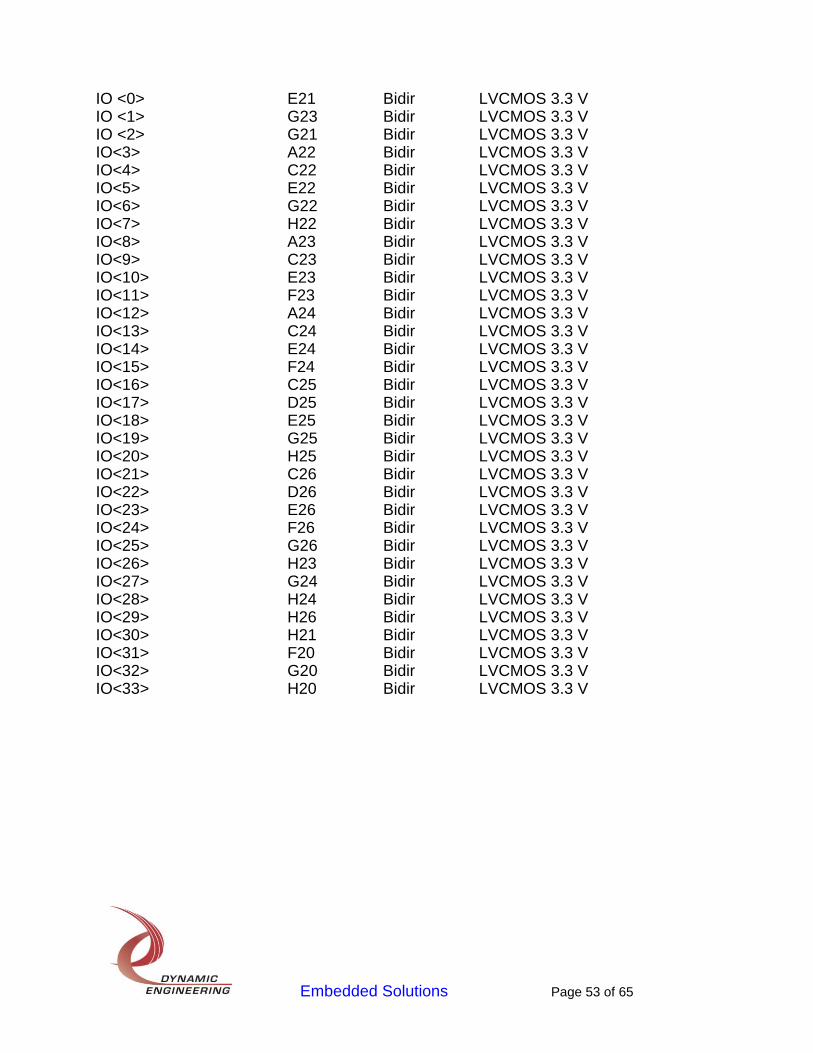
Embedded Solutions Page 53 of 65
IO <0> E21 Bidir LVCMOS 3.3 V IO <1> G23 Bidir LVCMOS 3.3 V IO <2> G21 Bidir LVCMOS 3.3 V IO<3> A22 Bidir LVCMOS 3.3 V IO<4> C22 Bidir LVCMOS 3.3 V IO<5> E22 Bidir LVCMOS 3.3 V IO<6> G22 Bidir LVCMOS 3.3 V IO<7> H22 Bidir LVCMOS 3.3 V IO<8> A23 Bidir LVCMOS 3.3 V IO<9> C23 Bidir LVCMOS 3.3 V IO<10> E23 Bidir LVCMOS 3.3 V IO<11> F23 Bidir LVCMOS 3.3 V IO<12> A24 Bidir LVCMOS 3.3 V IO<13> C24 Bidir LVCMOS 3.3 V IO<14> E24 Bidir LVCMOS 3.3 V IO<15> F24 Bidir LVCMOS 3.3 V IO<16> C25 Bidir LVCMOS 3.3 V IO<17> D25 Bidir LVCMOS 3.3 V IO<18> E25 Bidir LVCMOS 3.3 V IO<19> G25 Bidir LVCMOS 3.3 V IO<20> H25 Bidir LVCMOS 3.3 V IO<21> C26 Bidir LVCMOS 3.3 V IO<22> D26 Bidir LVCMOS 3.3 V IO<23> E26 Bidir LVCMOS 3.3 V IO<24> F26 Bidir LVCMOS 3.3 V IO<25> G26 Bidir LVCMOS 3.3 V IO<26> H23 Bidir LVCMOS 3.3 V IO<27> G24 Bidir LVCMOS 3.3 V IO<28> H24 Bidir LVCMOS 3.3 V IO<29> H26 Bidir LVCMOS 3.3 V IO<30> H21 Bidir LVCMOS 3.3 V IO<31> F20 Bidir LVCMOS 3.3 V IO<32> G20 Bidir LVCMOS 3.3 V IO<33> H20 Bidir LVCMOS 3.3 V
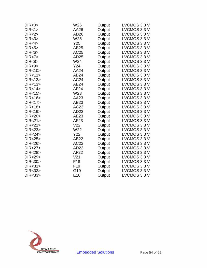
Embedded Solutions Page 54 of 65
DIR<0> W26 Output LVCMOS 3.3 V DIR<1> AA26 Output LVCMOS 3.3 V DIR<2> AD26 Output LVCMOS 3.3 V DIR<3> W25 Output LVCMOS 3.3 V DIR<4> Y25 Output LVCMOS 3.3 V DIR<5> AB25 Output LVCMOS 3.3 V DIR<6> AC25 Output LVCMOS 3.3 V DIR<7> AD25 Output LVCMOS 3.3 V DIR<8> W24 Output LVCMOS 3.3 V DIR<9> Y24 Output LVCMOS 3.3 V DIR<10> AA24 Output LVCMOS 3.3 V DIR<11> AB24 Output LVCMOS 3.3 V DIR<12> AC24 Output LVCMOS 3.3 V DIR<13> AE24 Output LVCMOS 3.3 V DIR<14> AF24 Output LVCMOS 3.3 V DIR<15> W23 Output LVCMOS 3.3 V DIR<16> AA23 Output LVCMOS 3.3 V DIR<17> AB23 Output LVCMOS 3.3 V DIR<18> AC23 Output LVCMOS 3.3 V DIR<19> AD23 Output LVCMOS 3.3 V DIR<20> AE23 Output LVCMOS 3.3 V DIR<21> AF23 Output LVCMOS 3.3 V DIR<22> V22 Output LVCMOS 3.3 V DIR<23> W22 Output LVCMOS 3.3 V DIR<24> Y22 Output LVCMOS 3.3 V DIR<25> AB22 Output LVCMOS 3.3 V DIR<26> AC22 Output LVCMOS 3.3 V DIR<27> AD22 Output LVCMOS 3.3 V DIR<28> AF22 Output LVCMOS 3.3 V DIR<29> V21 Output LVCMOS 3.3 V DIR<30> F18 Output LVCMOS 3.3 V DIR<31> F19 Output LVCMOS 3.3 V DIR<32> G19 Output LVCMOS 3.3 V DIR<33> E18 Output LVCMOS 3.3 V
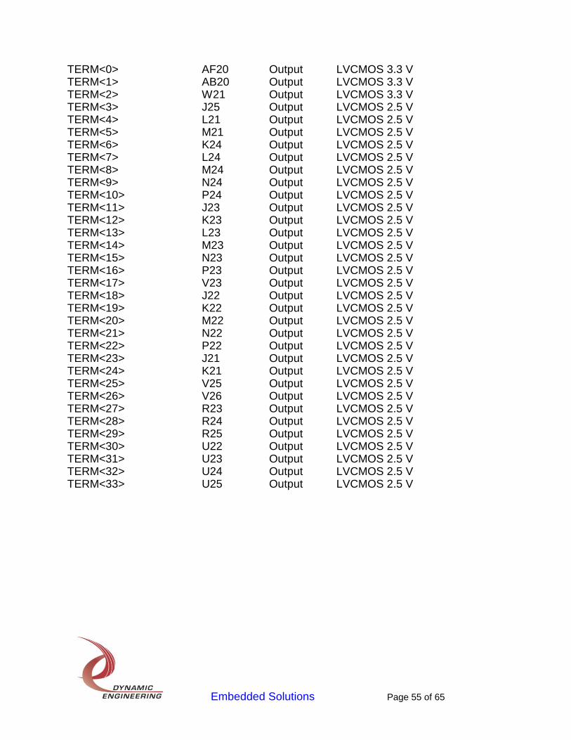
Embedded Solutions Page 55 of 65
TERM<0> AF20 Output LVCMOS 3.3 V TERM<1> AB20 Output LVCMOS 3.3 V TERM<2> W21 Output LVCMOS 3.3 V TERM<3> J25 Output LVCMOS 2.5 V TERM<4> L21 Output LVCMOS 2.5 V TERM<5> M21 Output LVCMOS 2.5 V TERM<6> K24 Output LVCMOS 2.5 V TERM<7> L24 Output LVCMOS 2.5 V TERM<8> M24 Output LVCMOS 2.5 V TERM<9> N24 Output LVCMOS 2.5 V TERM<10> P24 Output LVCMOS 2.5 V TERM<11> J23 Output LVCMOS 2.5 V TERM<12> K23 Output LVCMOS 2.5 V TERM<13> L23 Output LVCMOS 2.5 V TERM<14> M23 Output LVCMOS 2.5 V TERM<15> N23 Output LVCMOS 2.5 V TERM<16> P23 Output LVCMOS 2.5 V TERM<17> V23 Output LVCMOS 2.5 V TERM<18> J22 Output LVCMOS 2.5 V TERM<19> K22 Output LVCMOS 2.5 V TERM<20> M22 Output LVCMOS 2.5 V TERM<21> N22 Output LVCMOS 2.5 V TERM<22> P22 Output LVCMOS 2.5 V TERM<23> J21 Output LVCMOS 2.5 V TERM<24> K21 Output LVCMOS 2.5 V TERM<25> V25 Output LVCMOS 2.5 V TERM<26> V26 Output LVCMOS 2.5 V TERM<27> R23 Output LVCMOS 2.5 V TERM<28> R24 Output LVCMOS 2.5 V TERM<29> R25 Output LVCMOS 2.5 V TERM<30> U22 Output LVCMOS 2.5 V TERM<31> U23 Output LVCMOS 2.5 V TERM<32> U24 Output LVCMOS 2.5 V TERM<33> U25 Output LVCMOS 2.5 V
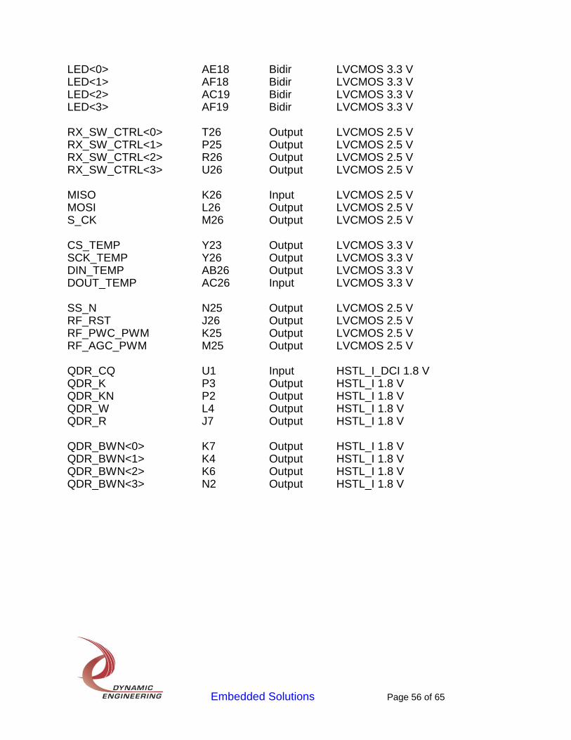
Embedded Solutions Page 56 of 65
LED<0> AE18 Bidir LVCMOS 3.3 V LED<1> AF18 Bidir LVCMOS 3.3 V LED<2> AC19 Bidir LVCMOS 3.3 V LED<3> AF19 Bidir LVCMOS 3.3 V RX_SW_CTRL<0> T26 Output LVCMOS 2.5 V RX_SW_CTRL<1> P25 Output LVCMOS 2.5 V RX_SW_CTRL<2> R26 Output LVCMOS 2.5 V RX_SW_CTRL<3> U26 Output LVCMOS 2.5 V MISO K26 Input LVCMOS 2.5 V MOSI L26 Output LVCMOS 2.5 V S_CK M26 Output LVCMOS 2.5 V CS_TEMP Y23 Output LVCMOS 3.3 V SCK_TEMP Y26 Output LVCMOS 3.3 V DIN_TEMP AB26 Output LVCMOS 3.3 V DOUT_TEMP AC26 Input LVCMOS 3.3 V SS_N N25 Output LVCMOS 2.5 V RF_RST J26 Output LVCMOS 2.5 V RF_PWC_PWM K25 Output LVCMOS 2.5 V RF_AGC_PWM M25 Output LVCMOS 2.5 V QDR_CQ U1 Input HSTL_I_DCI 1.8 V QDR_K P3 Output HSTL_I 1.8 V QDR_KN P2 Output HSTL_I 1.8 V QDR_W L4 Output HSTL_I 1.8 V QDR_R J7 Output HSTL_I 1.8 V QDR_BWN<0> K7 Output HSTL_I 1.8 V QDR_BWN<1> K4 Output HSTL_I 1.8 V QDR_BWN<2> K6 Output HSTL_I 1.8 V QDR_BWN<3> N2 Output HSTL_I 1.8 V
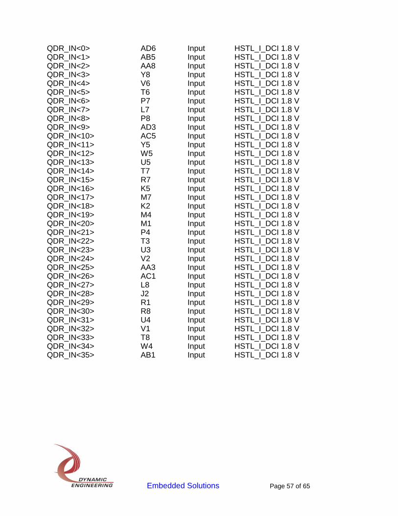
Embedded Solutions Page 57 of 65
QDR_IN<0> AD6 Input HSTL_I_DCI 1.8 V QDR_IN<1> AB5 Input HSTL_I_DCI 1.8 V QDR_IN<2> AA8 Input HSTL_I_DCI 1.8 V QDR_IN<3> Y8 Input HSTL_I_DCI 1.8 V QDR_IN<4> V6 Input HSTL_I_DCI 1.8 V QDR_IN<5> T6 Input HSTL_I_DCI 1.8 V QDR_IN<6> P7 Input HSTL_I_DCI 1.8 V QDR_IN<7> L7 Input HSTL_I_DCI 1.8 V QDR_IN<8> P8 Input HSTL_I_DCI 1.8 V QDR_IN<9> AD3 Input HSTL_I_DCI 1.8 V QDR_IN<10> AC5 Input HSTL_I_DCI 1.8 V QDR_IN<11> Y5 Input HSTL_I_DCI 1.8 V QDR_IN<12> W5 Input HSTL_I_DCI 1.8 V QDR_IN<13> U5 Input HSTL_I_DCI 1.8 V QDR_IN<14> T7 Input HSTL_I_DCI 1.8 V QDR_IN<15> R7 Input HSTL_I_DCI 1.8 V QDR_IN<16> K5 Input HSTL_I_DCI 1.8 V QDR_IN<17> M7 Input HSTL_I_DCI 1.8 V QDR_IN<18> K2 Input HSTL_I_DCI 1.8 V QDR_IN<19> M4 Input HSTL_I_DCI 1.8 V QDR_IN<20> M1 Input HSTL_I_DCI 1.8 V QDR_IN<21> P4 Input HSTL_I_DCI 1.8 V QDR_IN<22> T3 Input HSTL_I_DCI 1.8 V QDR_IN<23> U3 Input HSTL_I_DCI 1.8 V QDR_IN<24> V2 Input HSTL_I_DCI 1.8 V QDR_IN<25> AA3 Input HSTL_I_DCI 1.8 V QDR_IN<26> AC1 Input HSTL_I_DCI 1.8 V QDR_IN<27> L8 Input HSTL_I_DCI 1.8 V QDR_IN<28> J2 Input HSTL_I_DCI 1.8 V QDR_IN<29> R1 Input HSTL_I_DCI 1.8 V QDR_IN<30> R8 Input HSTL_I_DCI 1.8 V QDR_IN<31> U4 Input HSTL_I_DCI 1.8 V QDR_IN<32> V1 Input HSTL_I_DCI 1.8 V QDR_IN<33> T8 Input HSTL_I_DCI 1.8 V QDR_IN<34> W4 Input HSTL_I_DCI 1.8 V QDR_IN<35> AB1 Input HSTL_I_DCI 1.8 V
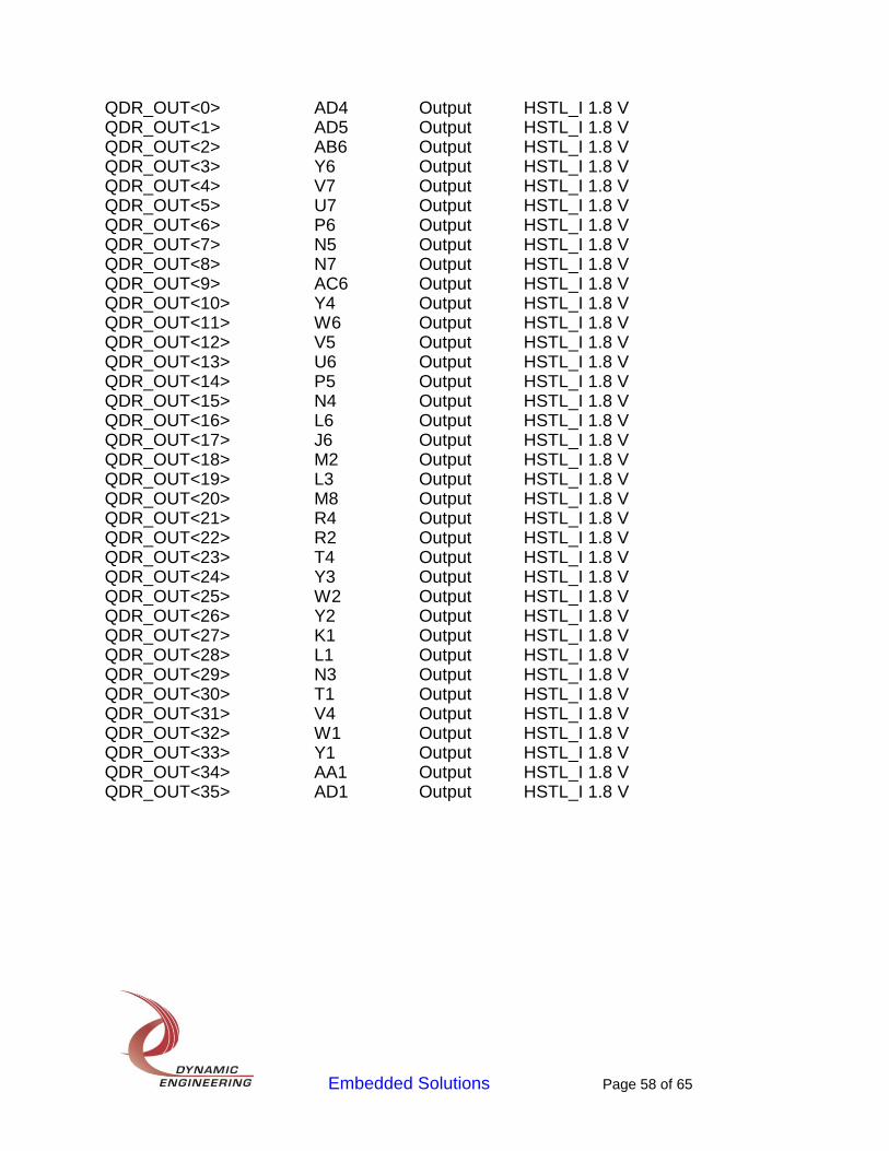
Embedded Solutions Page 58 of 65
QDR_OUT<0> AD4 Output HSTL_I 1.8 V QDR_OUT<1> AD5 Output HSTL_I 1.8 V QDR_OUT<2> AB6 Output HSTL_I 1.8 V QDR_OUT<3> Y6 Output HSTL_I 1.8 V QDR_OUT<4> V7 Output HSTL_I 1.8 V QDR_OUT<5> U7 Output HSTL_I 1.8 V QDR_OUT<6> P6 Output HSTL_I 1.8 V QDR_OUT<7> N5 Output HSTL_I 1.8 V QDR_OUT<8> N7 Output HSTL_I 1.8 V QDR_OUT<9> AC6 Output HSTL_I 1.8 V QDR_OUT<10> Y4 Output HSTL_I 1.8 V QDR_OUT<11> W6 Output HSTL_I 1.8 V QDR_OUT<12> V5 Output HSTL_I 1.8 V QDR_OUT<13> U6 Output HSTL_I 1.8 V QDR_OUT<14> P5 Output HSTL_I 1.8 V QDR_OUT<15> N4 Output HSTL_I 1.8 V QDR_OUT<16> L6 Output HSTL_I 1.8 V QDR_OUT<17> J6 Output HSTL_I 1.8 V QDR_OUT<18> M2 Output HSTL_I 1.8 V QDR_OUT<19> L3 Output HSTL_I 1.8 V QDR_OUT<20> M8 Output HSTL_I 1.8 V QDR_OUT<21> R4 Output HSTL_I 1.8 V QDR_OUT<22> R2 Output HSTL_I 1.8 V QDR_OUT<23> T4 Output HSTL_I 1.8 V QDR_OUT<24> Y3 Output HSTL_I 1.8 V QDR_OUT<25> W2 Output HSTL_I 1.8 V QDR_OUT<26> Y2 Output HSTL_I 1.8 V QDR_OUT<27> K1 Output HSTL_I 1.8 V QDR_OUT<28> L1 Output HSTL_I 1.8 V QDR_OUT<29> N3 Output HSTL_I 1.8 V QDR_OUT<30> T1 Output HSTL_I 1.8 V QDR_OUT<31> V4 Output HSTL_I 1.8 V QDR_OUT<32> W1 Output HSTL_I 1.8 V QDR_OUT<33> Y1 Output HSTL_I 1.8 V QDR_OUT<34> AA1 Output HSTL_I 1.8 V QDR_OUT<35> AD1 Output HSTL_I 1.8 V
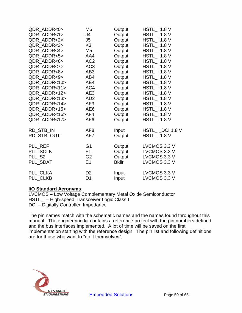
Embedded Solutions Page 59 of 65
QDR_ADDR<0> M6 Output HSTL_I 1.8 V QDR_ADDR<1> J4 Output HSTL_I 1.8 V QDR_ADDR<2> J5 Output HSTL_I 1.8 V QDR_ADDR<3> K3 Output HSTL_I 1.8 V QDR_ADDR<4> M5 Output HSTL_I 1.8 V QDR_ADDR<5> AA4 Output HSTL_I 1.8 V QDR_ADDR<6> AC2 Output HSTL_I 1.8 V QDR_ADDR<7> AC3 Output HSTL_I 1.8 V QDR_ADDR<8> AB3 Output HSTL_I 1.8 V QDR_ADDR<9> AB4 Output HSTL_I 1.8 V QDR_ADDR<10> AE4 Output HSTL_I 1.8 V QDR_ADDR<11> AC4 Output HSTL_I 1.8 V QDR_ADDR<12> AE3 Output HSTL_I 1.8 V QDR_ADDR<13> AD2 Output HSTL_I 1.8 V QDR_ADDR<14> AF3 Output HSTL_I 1.8 V QDR_ADDR<15> AE6 Output HSTL_I 1.8 V QDR_ADDR<16> AF4 Output HSTL_I 1.8 V QDR_ADDR<17> AF6 Output HSTL_I 1.8 V RD_STB_IN AF8 Input HSTL_I_DCI 1.8 V RD_STB_OUT AF7 Output HSTL_I 1.8 V PLL_REF G1 Output LVCMOS 3.3 V PLL_SCLK F1 Output LVCMOS 3.3 V PLL_S2 G2 Output LVCMOS 3.3 V PLL_SDAT E1 Bidir LVCMOS 3.3 V PLL_CLKA D2 Input LVCMOS 3.3 V PLL_CLKB D1 Input LVCMOS 3.3 V I/O Standard Acronyms: LVCMOS – Low Voltage Complementary Metal Oxide Semiconductor HSTL_I – High-speed Transceiver Logic Class I DCI – Digitally Controlled Impedance The pin names match with the schematic names and the names found throughout this manual. The engineering kit contains a reference project with the pin numbers defined and the bus interfaces implemented. A lot of time will be saved on the first implementation starting with the reference design. The pin list and following definitions are for those who want to “do it themselves”.
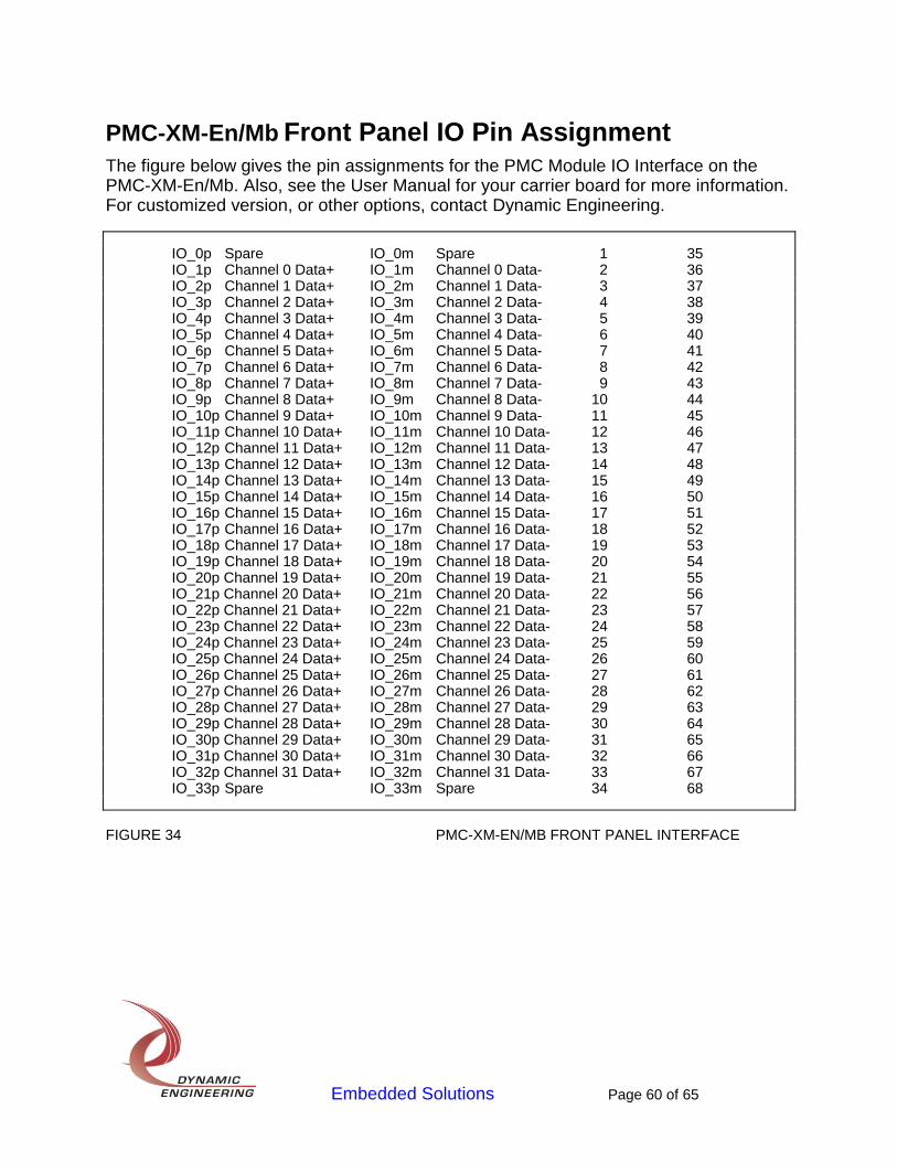
Embedded Solutions Page 60 of 65
PMC-XM-En/Mb Front Panel IO Pin Assignment The figure below gives the pin assignments for the PMC Module IO Interface on the PMC-XM-En/Mb. Also, see the User Manual for your carrier board for more information. For customized version, or other options, contact Dynamic Engineering.
IO_0p Spare IO_0m Spare 1 35 IO_1p Channel 0 Data+ IO_1m Channel 0 Data- 2 36 IO_2p Channel 1 Data+ IO_2m Channel 1 Data- 3 37 IO_3p Channel 2 Data+ IO_3m Channel 2 Data- 4 38 IO_4p Channel 3 Data+ IO_4m Channel 3 Data- 5 39 IO_5p Channel 4 Data+ IO_5m Channel 4 Data- 6 40 IO_6p Channel 5 Data+ IO_6m Channel 5 Data- 7 41 IO_7p Channel 6 Data+ IO_7m Channel 6 Data- 8 42 IO_8p Channel 7 Data+ IO_8m Channel 7 Data- 9 43 IO_9p Channel 8 Data+ IO_9m Channel 8 Data- 10 44 IO_10p Channel 9 Data+ IO_10m Channel 9 Data- 11 45 IO_11p Channel 10 Data+ IO_11m Channel 10 Data- 12 46 IO_12p Channel 11 Data+ IO_12m Channel 11 Data- 13 47 IO_13p Channel 12 Data+ IO_13m Channel 12 Data- 14 48 IO_14p Channel 13 Data+ IO_14m Channel 13 Data- 15 49 IO_15p Channel 14 Data+ IO_15m Channel 14 Data- 16 50 IO_16p Channel 15 Data+ IO_16m Channel 15 Data- 17 51 IO_17p Channel 16 Data+ IO_17m Channel 16 Data- 18 52 IO_18p Channel 17 Data+ IO_18m Channel 17 Data- 19 53 IO_19p Channel 18 Data+ IO_19m Channel 18 Data- 20 54 IO_20p Channel 19 Data+ IO_20m Channel 19 Data- 21 55 IO_21p Channel 20 Data+ IO_21m Channel 20 Data- 22 56 IO_22p Channel 21 Data+ IO_22m Channel 21 Data- 23 57 IO_23p Channel 22 Data+ IO_23m Channel 22 Data- 24 58 IO_24p Channel 23 Data+ IO_24m Channel 23 Data- 25 59 IO_25p Channel 24 Data+ IO_25m Channel 24 Data- 26 60 IO_26p Channel 25 Data+ IO_26m Channel 25 Data- 27 61 IO_27p Channel 26 Data+ IO_27m Channel 26 Data- 28 62 IO_28p Channel 27 Data+ IO_28m Channel 27 Data- 29 63 IO_29p Channel 28 Data+ IO_29m Channel 28 Data- 30 64 IO_30p Channel 29 Data+ IO_30m Channel 29 Data- 31 65 IO_31p Channel 30 Data+ IO_31m Channel 30 Data- 32 66 IO_32p Channel 31 Data+ IO_32m Channel 31 Data- 33 67 IO_33p Spare IO_33m Spare 34 68
FIGURE 34 PMC-XM-EN/MB FRONT PANEL INTERFACE

Embedded Solutions Page 61 of 65
Applications Guide
Interfacing
Some general interfacing guidelines are presented below. Do not hesitate to contact the factory if you need more assistance. ESD Proper ESD handling procedures must be followed when handling the PMC-XM. The card is shipped in an anti-static, shielded bag. The card should remain in the bag until ready for use. When installing the card the installer must be properly grounded and the hardware should be on an anti-static work-station. Start-up Make sure that the "system" can see your hardware before trying to access it. Many BIOS will display the PCI devices found at boot up on a "splash screen" with the VendorID and CardId and an interrupt level. Look quickly! If the information is not available from the BIOS, a third party PCI device cataloging tool can be used to identify the installed PCI devices. We use PCIView. Watch the system grounds. All electrically connected equipment should have a fail-safe common ground that is large enough to handle all current loads without affecting noise immunity. Power supplies and power consuming loads should all have their own ground wires back to a common point. We provide the components. You provide the system. Only careful planning and practice can achieve safety and reliability. Inputs can be damaged by static discharge, or by applying voltage outside of the device rated voltages.

Embedded Solutions Page 62 of 65
Construction and Reliability
PMC Modules were conceived and engineered for rugged industrial environments. The PMC-XM is constructed out of 0.062-inch thick FR4 material. Surface-mount components are used. The PMC connectors are rated at 1 Amp per pin, 100 insertion cycles minimum. These connectors make consistent, correct insertion easy and reliable. The PMC is secured against the carrier with four screws attached to the 2 stand-offs and 2 locations on the front panel. The four screws provide significant protection against shock, vibration, and incomplete insertion.
The PMC Module provides a low temperature coefficient of 2.17 W/ C for uniform heat. This is based upon the temperature coefficient of the base FR4 material of 0.31 W/m-
C, and taking into account the thickness and area of the PMC. The coefficient means that if 2.17 Watts are applied uniformly on the component side, then the temperature difference between the component side and solder side is one degree Celsius.
Thermal Considerations
The PMC-XM design consists of CMOS circuits. The power dissipation due to internal circuitry is very low. It is possible to create higher power dissipation with the externally connected logic. If more than one Watt is required to be dissipated due to external loading, then forced-air cooling is recommended. With the one degree differential temperature to the solder side of the board, external cooling is easily accomplished.

Embedded Solutions Page 63 of 65
Warranty and Repair
Please refer to the warranty page on our website for the current warranty offered and options. http://www.dyneng.com/warranty.html
Service Policy
Before returning a product for repair, verify as well as possible that the suspected unit is at fault. Then call the Customer Service Department for a RETURN MATERIAL AUTHORIZATION (RMA) number. Carefully package the unit, in the original shipping carton if this is available, and ship prepaid and insured with the RMA number clearly written on the outside of the package. Include a return address and the telephone number of a technical contact. For out-of-warranty repairs, a purchase order for repair charges must accompany the return. Dynamic Engineering will not be responsible for damages due to improper packaging of returned items. For service on Dynamic Engineering Products not purchased directly from Dynamic Engineering contact your reseller. Products returned to Dynamic Engineering for repair by other than the original customer will be treated as out-of-warranty.
Out of Warranty Repairs
Out of warranty repairs will be billed on a material and labor basis. The current minimum repair charge is $100. Customer approval will be obtained before repairing any item if the repair charges will exceed one half of the quantity one list price for that unit. Return transportation and insurance will be billed as part of the repair and is in addition to the minimum charge.
For Service Contact:
Customer Service Department Dynamic Engineering 150 DuBois, Suite C Santa Cruz, CA 95060 (831) 457-8891 Fax (831) 457-4793 [email protected]
Embedded Solutions Page 64 of 65
Specifications Host Interface: 33 MHz/32-bit PCI Mezzanine Card Access types: Configuration and Memory space utilized Clock rates supported: 33 MHz. PMC, 33 MHz data transfer between Spartan3 and Virtex
Local 40 MHz oscillator for PLL reference to provide two programmable frequencies
Memory Four 4K x 32-bit FIFOs are provided to support DMA on the Spartan3 and 64 1K
x 32-bit FIFOs on the Virtex for the 32 I/O channels Software Interface: Control/Status Registers within Spartan3 and Virtex Initialization: Hardware reset forces all registers to zero except as noted Access Modes: All registers on long-word boundary - Standard target accesses read and write to
registers and memory - DMA access to memory Access Time: No wait states in DMA modes, one wait state in target access to Spartan3
Virtex accesses are user defined Interrupt: One interrupt to the PCI bus is supported with multiple sources. The interrupts
are maskable and are supported with status registers. Onboard Options: All Options are Software Programmable. Dimensions: Standard Single PMC Module Construction: FR4 Multi-Layer Printed Circuit, Surface Mount Components Power: 5V and 3.3V from PCI bus. Local 2.5V, 1.8V and 1.2V created with on-
board power supplies User 8 position software readable switch
4 software controllable LEDs 2 Power LEDs
Embedded Solutions Page 65 of 65
Order Information
PMC-XM http://www.dyneng.com/pmc_xm.html Standard version with two 16KB FIFOs per channel, standard XM timing and protocol.
PMC-XM-Eng-1 Engineering Kit for the PMC-XM Board-level schematics (PDF) and Sample Virtex design (VHDL)
PMC-XM-Eng-2 Engineering Kit for the PMC-XM Board-level schematics [PDF], Sample Virtex Design (VHDL), Software Drivers and Sample Test Application
All information provided is Copyright Dynamic Engineering


![DPU2000/1500R/2000R MODBUS / MODBUS PLUS … · DPU2000/1500R/2000R Modbus/Modbus Plus Automation Guide i DPU2000/1500R/2000R MODBUS / MODBUS PLUS ... [Catalog 587XXX00-XXX0 or 587XXXX6-XXX4]](https://img.pdfslide.net/doc/110x75/5acb9eac7f8b9a73128bdc42/dpu20001500r2000r-modbus-modbus-plus-modbusmodbus-plus-automation-guide.jpg)


![MODBUS IINDUSTRIE sWETTERSTATIONNDUSTRIE …€¦ · MODBUS rain[e]one Modbus INDUSTRY Modbus Pyranometer THP[pro] Modbus rain one Modbus IN Wiegender Nieder-schlagssensor Windrichtung](https://img.pdfslide.net/doc/110x75/5eb88fa576fba607cd617fd5/modbus-iindustrie-swetterstationndustrie-modbus-raineone-modbus-industry-modbus.jpg)